debugging the n2pk vna dave roberts, g8kbb
TRANSCRIPT
Debugging the N2PK VNA
Version 0.3 Page 1 of 34
Debugging the N2PK VNA
Dave Roberts, G8KBB
This document is intended for people who have built an N2PK VNA and are having
difficulty getting it working
For clarity, throughout this document, the term ‘VNA’ will be used to refer to the N2PK
VNA, either in its original ExpressPCB form or in Ivan’s 4.x series boards.
This document is not a panacea for all evils. If you use it and find that it does not solve
your problems, please propose extensions to it with your eventual solution in order to
help others. If you find errors, tell me.
The document is divided into different sections that relate to different aspects. Be
prepared to flip from section to section as you chase your gremlins
The document presumes a certain level of understanding. If you don’t follow the
meaning, seek the services of a local ham who can help. As a test, read the following
bullet pointed items. If the following is meaningless gibberish to you, don’t even bother
trying to understand this document – seek help from a local ham.
• The hardware settings for a parallel port may be accessed by double clicking on
the “System” icon in Control Panel, then selecting “Hardware” from the options
and clicking on “Device Manager”
• Use an oscilloscope to view the signal on the DDS FQ_UD line.
An assumption that is made in this document is that people are more likely to be
conversant with hardware than with getting the PC to drive the hardware, so hardware
debugging information is minimal.
Finally note that this document is NOT going to explain everything about computers and
electronics, and is not a replacement for the manuals that have been produced for the
application software such as myVNA, Exeter, VNA4win and Paul’s programs.
Debugging the N2PK VNA
Version 0.3 Page 2 of 34
Contents
1 Start Here .................................................................................................................... 3
2 Debugging the VNA Hardware .................................................................................. 4
Launching your v4.1 board ..................................................................................... 4
3 Parallel ports ............................................................................................................... 5
3.1 Connectors and Cables........................................................................................ 5
3.2 Port Addresses and Port Types ........................................................................... 7
3.3 Port assignments ................................................................................................. 8
3.4 DOS..................................................................................................................... 9
3.4.1 The lowest level possible .......................................................................... 12
3.5 Windows ........................................................................................................... 12
3.5.1 DOSbox..................................................................................................... 13
3.5.2 Direct I/O .................................................................................................. 14
3.5.3 Debugging Parallel Ports with myVNA ................................................... 14
3.6 Other Parallel Port Issues.................................................................................. 17
3.6.1 Uninitialised ports problem....................................................................... 17
3.6.2 Glitches in Operation ................................................................................ 18
3.6.3 Port Type................................................................................................... 19
3.7 Other Operating Systems .................................................................................. 20
4 USB port ................................................................................................................... 20
4.1 Hardware issues ................................................................................................ 20
4.2 USB Configuration ........................................................................................... 24
4.2.1 USBview................................................................................................... 25
4.2.2 USB Configure.......................................................................................... 26
4.3 Upgrading drivers ............................................................................................. 28
4.4 Windows ........................................................................................................... 28
4.5 Other Operating Systems .................................................................................. 30
5 Paul’s Programs ........................................................................................................ 30
6 myVNA..................................................................................................................... 30
7 VNA4win.................................................................................................................. 31
8 Exeter ........................................................................................................................ 33
9 VNAView ................................................................................................................. 34
Debugging the N2PK VNA
Version 0.3 Page 3 of 34
1 Start Here
OK, you built the VNA, carefully applied power, connected it to your PC, installed one
of the programs and…….
…… nothing.
This document aims to help you fault find. It is not exhaustive, but if you spot useful
additions that may help others, propose a change to improve it. Suggestions that do not
include proposed new text will be studiously ignored.
The basic testing process proposed is as follows
1. Follow the basic hardware tests in Section 2 ”Debugging the VNA Hardware”
2. Install whichever software package you intend to use
3. Try the whole thing. If it works, great, if not, follow the next set of steps
4. For whichever port you are using, parallel or USB, skip to the appropriate section
of this document (Section 3 for parallel ports or Section 4 for USB) and follow
that section in sequence. The aim of these sections is to start at the most basic
level and work upwards to test communications
5. Once communications has been established use Paul’s DOS programs, myVNA,
VNA4win or Exeter to test the VNA
The test strategy we are following here is, having checked the basic hardware and
installed a software package, to then debug the software sufficient to see that I/O lines
can be set high or low. The software is then used to debug the connectivity to the VNA
and the operation of the VNA.
So start with the next section……
Debugging the N2PK VNA
Version 0.3 Page 4 of 34
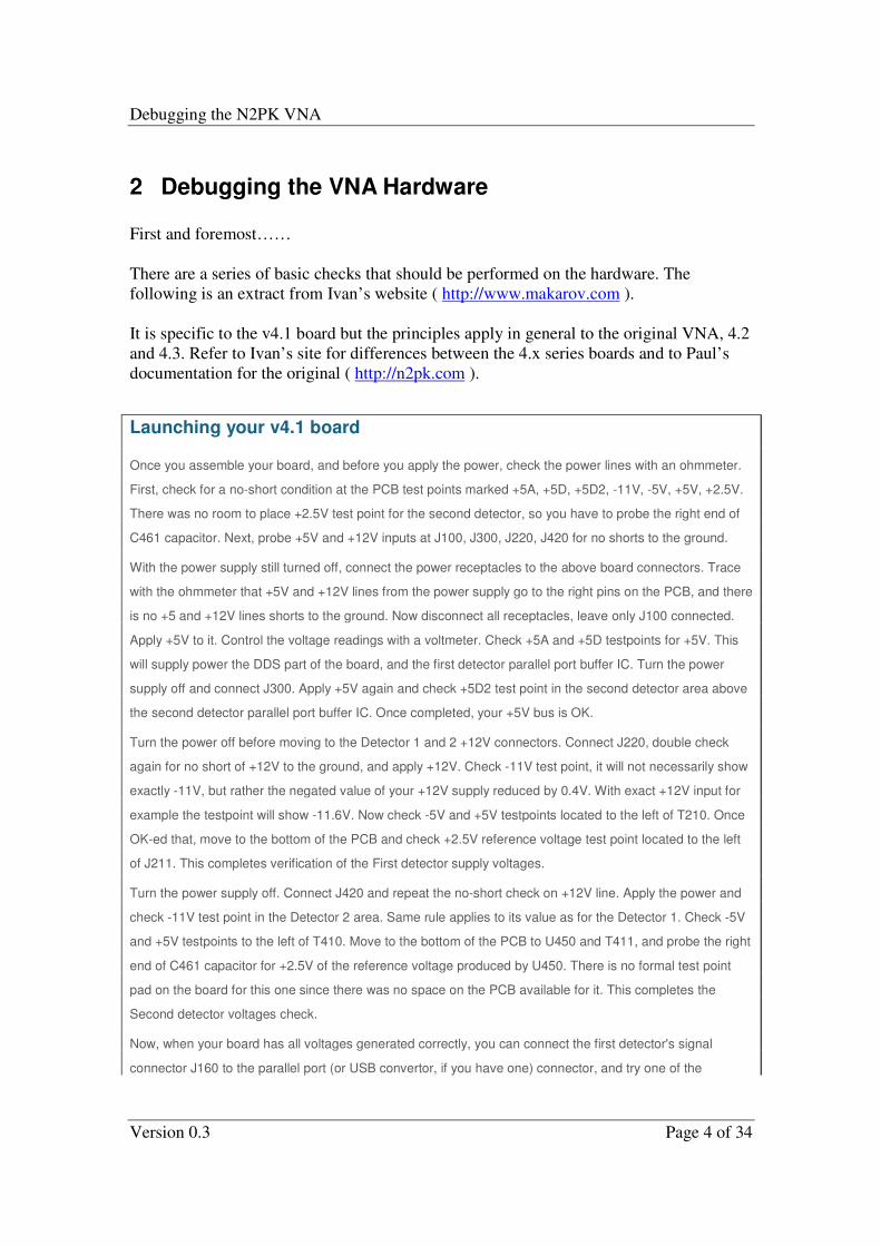
2 Debugging the VNA Hardware
First and foremost……
There are a series of basic checks that should be performed on the hardware. The
following is an extract from Ivan’s website ( http://www.makarov.com ).
It is specific to the v4.1 board but the principles apply in general to the original VNA, 4.2
and 4.3. Refer to Ivan’s site for differences between the 4.x series boards and to Paul’s
documentation for the original ( http://n2pk.com ).
Launching your v4.1 board
Once you assemble your board, and before you apply the power, check the power lines with an ohmmeter.
First, check for a no-short condition at the PCB test points marked +5A, +5D, +5D2, -11V, -5V, +5V, +2.5V.
There was no room to place +2.5V test point for the second detector, so you have to probe the right end of
C461 capacitor. Next, probe +5V and +12V inputs at J100, J300, J220, J420 for no shorts to the ground.
With the power supply still turned off, connect the power receptacles to the above board connectors. Trace
with the ohmmeter that +5V and +12V lines from the power supply go to the right pins on the PCB, and there
is no +5 and +12V lines shorts to the ground. Now disconnect all receptacles, leave only J100 connected.
Apply +5V to it. Control the voltage readings with a voltmeter. Check +5A and +5D testpoints for +5V. This
will supply power the DDS part of the board, and the first detector parallel port buffer IC. Turn the power
supply off and connect J300. Apply +5V again and check +5D2 test point in the second detector area above
the second detector parallel port buffer IC. Once completed, your +5V bus is OK.
Turn the power off before moving to the Detector 1 and 2 +12V connectors. Connect J220, double check
again for no short of +12V to the ground, and apply +12V. Check -11V test point, it will not necessarily show
exactly -11V, but rather the negated value of your +12V supply reduced by 0.4V. With exact +12V input for
example the testpoint will show -11.6V. Now check -5V and +5V testpoints located to the left of T210. Once
OK-ed that, move to the bottom of the PCB and check +2.5V reference voltage test point located to the left
of J211. This completes verification of the First detector supply voltages.
Turn the power supply off. Connect J420 and repeat the no-short check on +12V line. Apply the power and
check -11V test point in the Detector 2 area. Same rule applies to its value as for the Detector 1. Check -5V
and +5V testpoints to the left of T410. Move to the bottom of the PCB to U450 and T411, and probe the right
end of C461 capacitor for +2.5V of the reference voltage produced by U450. There is no formal test point
pad on the board for this one since there was no space on the PCB available for it. This completes the
Second detector voltages check.
Now, when your board has all voltages generated correctly, you can connect the first detector's signal
connector J160 to the parallel port (or USB convertor, if you have one) connector, and try one of the

Debugging the N2PK VNA
Version 0.3 Page 5 of 34
available VNA programs to talk to the VNA. Make sure you can do this before you try the second detector.
Once your Detector 1 supplies the data to the VNA program, connect J360, run the program again and
make sure it sees the Detector 2.
To verify the DDS functionality, hook up a counter or a scope to J170 (RF DDS), J120 or J180 (LO DDS).
Run the software and watch the signal changed once you vary it from the software. You may also want to
check the master oscillator buffer IC at J150, which outputs the signal at the master oscillator frequency.
Refer to the VNA schematics for the values of the output signals.
Before starting probing the VNA functionality in either reflection or transmission modes with one of the
available programs, connect the LO DDS outputs to the detectors inputs with the coaxial SMA male-male
jumpers from J120 to J410, and from J180 to J210. Alternatively, you can make use of the on-board
microstrip lines by soldering the corresponding jumpers.
If the above does not solves your problems then proceed to section 3 “Parallel ports” if
you are using a parallel port to connect to the VNA or Section 4 “USB port” if using the
USB interface for initial software testing information.
3 Parallel ports
This is the place to start from if you are using the Parallel port and, having completed the
basic hardware checks of Section 2, it is still not working.
When using the parallel port, there are a number of basic problems that may occur
• The cable may not be correct for the application
• The software may not be able to communicate with the port
• The address of the port may be incorrect
• There may be a fault on the VNA PCB
• You may be using the diagnostic programs incorrectly
Use the following sections to step though these issues
3.1 Connectors and Cables
The parallel port used to connect the VNA to the computer must follow the IEEE 1284
standard and the cable used should be an IEEE 1284 compliant one.
First check that your cable is of good quality and without damage to the pins. Then check
the cabling to ensure that all the pins needed by the VNA are in fact connected. Sounds
silly but check it!
The following are from Paul’s documentation ( http://n2pk.com )
Debugging the N2PK VNA
Version 0.3 Page 6 of 34
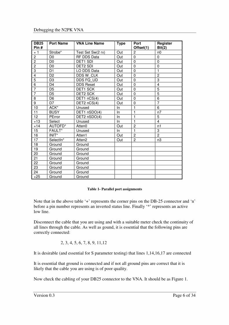
DB25 Port Name VNA Line Name Type Port Register Pin # Offset(1) Bit(2)
+ 1 Strobe* Test Set Sw(2 rx) Out 2 n0
2 D0 RF DDS Data Out 0 0
2 D0 DET1 SDI Out 0 0
2 D0 DET2 SDI Out 0 0
3 D1 LO DDS Data Out 0 1
4 D2 DDS W_CLK Out 0 2
5 D3 DDS FQ_UD Out 0 3
6 D4 DDS Reset Out 0 4
7 D5 DET1 SCK Out 0 5
7 D5 DET2 SCK Out 0 5
8 D6 DET1 nCS(4) Out 0 6
9 D7 DET2 nCS(4) Out 0 7
10 ACK* Unused In 1 6
11 BUSY DET1 nSDO(4) In 1 n7
12 PError DET2 nSDO(4) In 1 5
+13 Select Unused In 1 4
+14 AUTOFD* Atten0 Out 2 n1
15 FAULT* Unused In 1 3
16 INIT* Atten1 Out 2 2
17 SelectIn* Atten2 Out 2 n3
18 Ground Ground
19 Ground Ground
20 Ground Ground
21 Ground Ground
22 Ground Ground
23 Ground Ground
24 Ground Ground
+25 Ground Ground
Table 1- Parallel port assignments
Note that in the above table ‘+’ represents the corner pins on the DB-25 connector and ‘n’
before a pin number represents an inverted status line. Finally ‘*’ represents an active
low line.
Disconnect the cable that you are using and with a suitable meter check the continuity of
all lines through the cable. As well as gound, it is essential that the following pins are
correctly connected:
2, 3, 4, 5, 6, 7, 8, 9, 11,12
It is desirable (and essential for S parameter testing) that lines 1,14,16,17 are connected
It is essential that ground is connected and if not all ground pins are correct that it is
likely that the cable you are using is of poor quality.
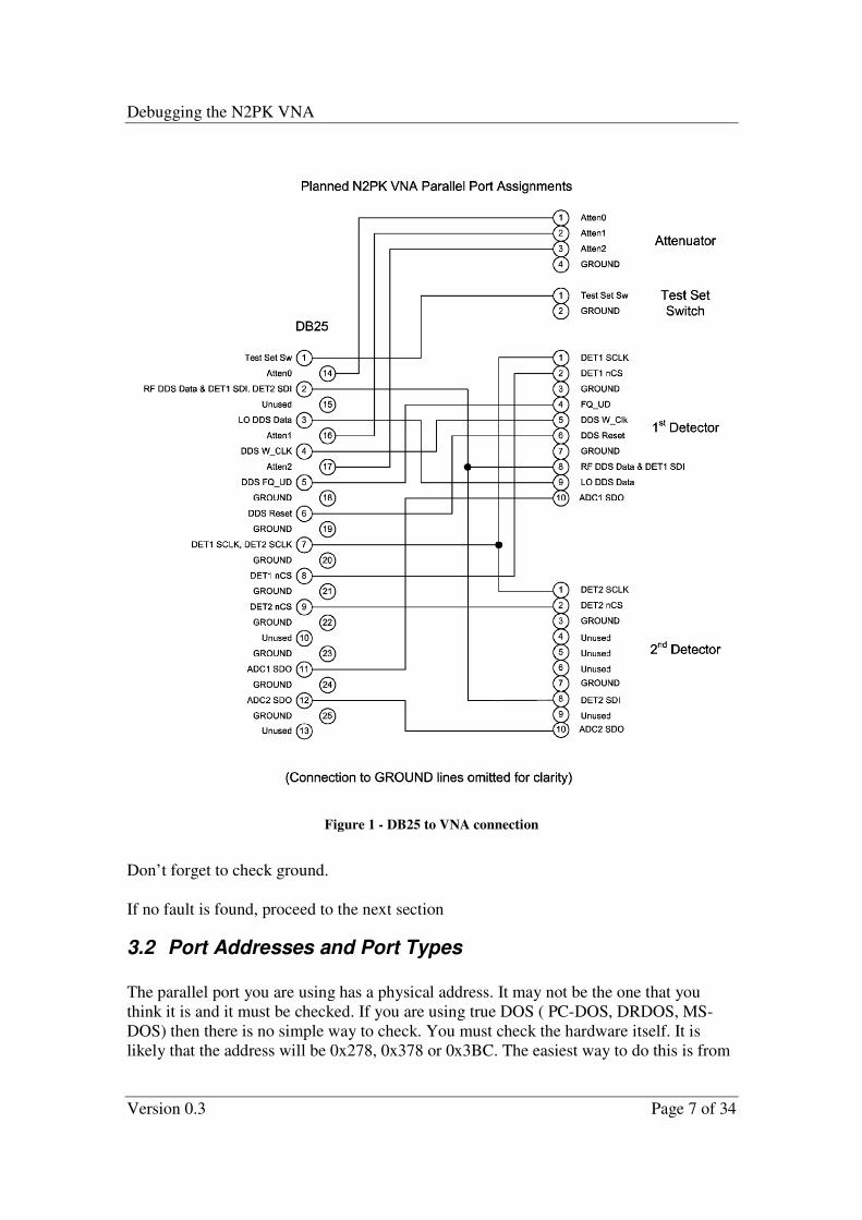
Now check the cabling of your DB25 connector to the VNA. It should be as Figure 1.
Debugging the N2PK VNA
Version 0.3 Page 7 of 34
Figure 1 - DB25 to VNA connection
Don’t forget to check ground.
If no fault is found, proceed to the next section
3.2 Port Addresses and Port Types
The parallel port you are using has a physical address. It may not be the one that you
think it is and it must be checked. If you are using true DOS ( PC-DOS, DRDOS, MS-
DOS) then there is no simple way to check. You must check the hardware itself. It is
likely that the address will be 0x278, 0x378 or 0x3BC. The easiest way to do this is from

Debugging the N2PK VNA
Version 0.3 Page 8 of 34
the BIOS. Unfortunately all BIOSes are different as are the keys to press to access the
BIOS. If you do not know, check the computer documentation, or if all else fails try F2,
ESC, DEL, F10 or F12 when the computer starts to boot. If you can’t do this or don’t
understand this, then do not seek for answers here – you will not find such a level of
detail – seek help from a local ham.
If the operating system is Windows, then device properties may be used to check the port
addresses. This may be accessed from “System” in “Control Panel” under “Hardware”
and “Device Manager”. Note that the exact details of this differ between operating
systems.
If you are stumped by this step, then stop here and find someone local who can navigate
their way round windows. This guide will not provide such a low level of details.
OK, continuing with the same assumption of a working understanding of computers, we
will proceed…..
From Device Manager open up “Ports (COM & LPT)” select the parallel port that you
are using and check its properties (again the caveat – if you do not know how to do this
do not seek for an answer in this document – you will not find it – seek a local ham who
can help you). “Resources” will indicate the base address – take a note of it as that is the
address to use. Ignore extended addresses associated with ECP ports, you are seeking just
the base address and it will be one of those shown above.
Finally, whilst you are here, check the port configuration. Whilst it should not matter, the
most flexible setting is ECP. This is normally set in the BIOS. See however the warning
from Roderick in Section 3.6.3, “Port Type”.
3.3 Port assignments
Section 3.2 above describes how to investigate hardware port addresses. The operating
system will map this address onto a logical name such as “LPT1”. This is a logical
“convenience” but does not really help. Under Windows most VNA software will need to
bypass the operating system and go directly (or as directly as it can) to the hardware port
addresses. Therefore whenever a logical name such as “LPT1” is used in VNA software
it is usually there only to “reserve” the port and stop other windows software from trying
to access the port whilst the VNA is using it.
In myVNA and Exeter, the parallel port address is set via the windows GUI. In Paul’s
programs and VNA4win it is set via a text configuration file.
In both cases you need to make sure it is correctly set.
Note also that if you have problems with low level communications, see the section 3.6.3
“Port Type”.

Debugging the N2PK VNA
Version 0.3 Page 9 of 34
3.4 DOS
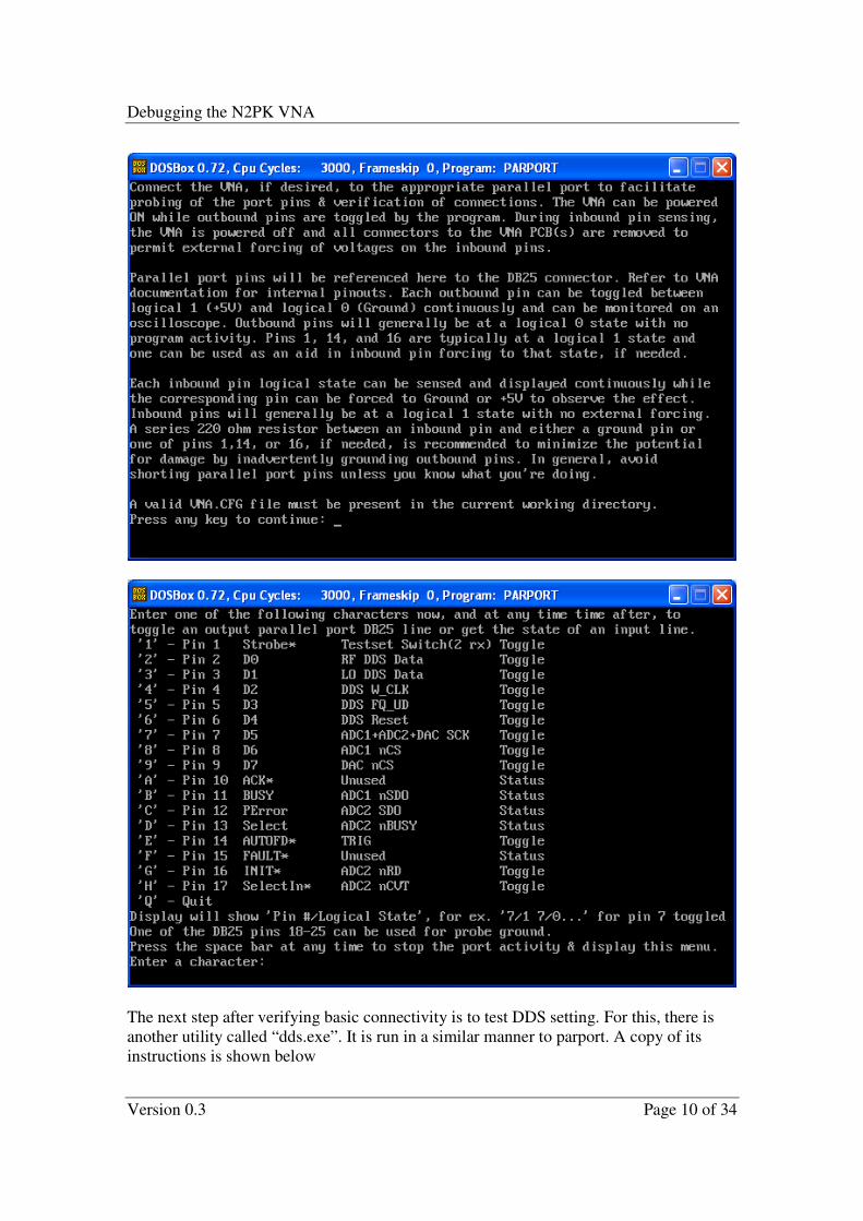
To debug a parallel port from DOS, the recommended way is to use Paul’s ParPort
program.
This program allows each of the parallel port output lines to be toggled high or low and
shows the status of each input line.
The program gives step by step guidance as it is run; follow its instructions. Note that to
operate correctly there must be a valid vna.cfg file present in the same directory as
parport and it must specify the correct port address.
Here is an example of a file. Comments have been shortened for clarity. The only entry to
worry about is the Port address.
Port=0x378 (Hex, set this to the address of the parallel port used by the VNA)
Clk=148.344 (MHz, set to the actual master oscillator frequency for the VNA)
ADCdel=10 (ms, delay between frequency program and first ADC read)
cfp=1 (set to '1' for Continuous Frequency Programming, '0' otherwise)
Z0=50 (ohms, basis for reflection coefficients and center of Smith Chart)
Cop=0.039 (0.039 pF for open flat ground female SMA chassis connector)
Rsh=0 (0 ohms for a short cal std on a flat ground female SMA)
Lsh=0.0 (0.00 nH for the SMA short cal std, series inductance of the Short)
Rld=50.000 (Series resistance of the Load cal standard, usually about 50 ohms)
Lld=0.15 (0.15 nH for 4x200 ohm 0805 on flat ground female SMA chassis connector)
Cld=0.23 (0.23 pF for the female SMA load std, excess shunt.)
Raw=0 (set to '1' to append raw data to *.RAW files, '0' if not)
The aim of the testing is to verify that when the program thinks it is setting or clearing a
specific line, that line on the connector is indeed set high or low.
Therefore proceed as follows:
For each output line in turn in Table 1- Parallel port assignments, verify that when the
software sets or clears this bit the corresponding pin on the connector is raised or
lowered. Then verify that for each input line when the line is pulled high or low, reading
the appropriate port shows a ‘1’ or a ‘0’.
Having verified that the output lines can be controlled or read, connect the cable to the
VNA and repeat the testing, tracing the signals on the VNA to check that the signals
reach the correct pins on the chips on the PCB.
If the output lines on the parallel port do not change state correctly, check first the port
address, then the hardware. Then check in the BIOS that the parallel port is enabled (it is
possible it has been disabled). There is one additional low level method to try as indicated
in the next section. If this does not work, then the most likely causes are bad connectors,
bad cables or faulty hardware.
A copy of the program’s instructions is shown below
Debugging the N2PK VNA
Version 0.3 Page 10 of 34
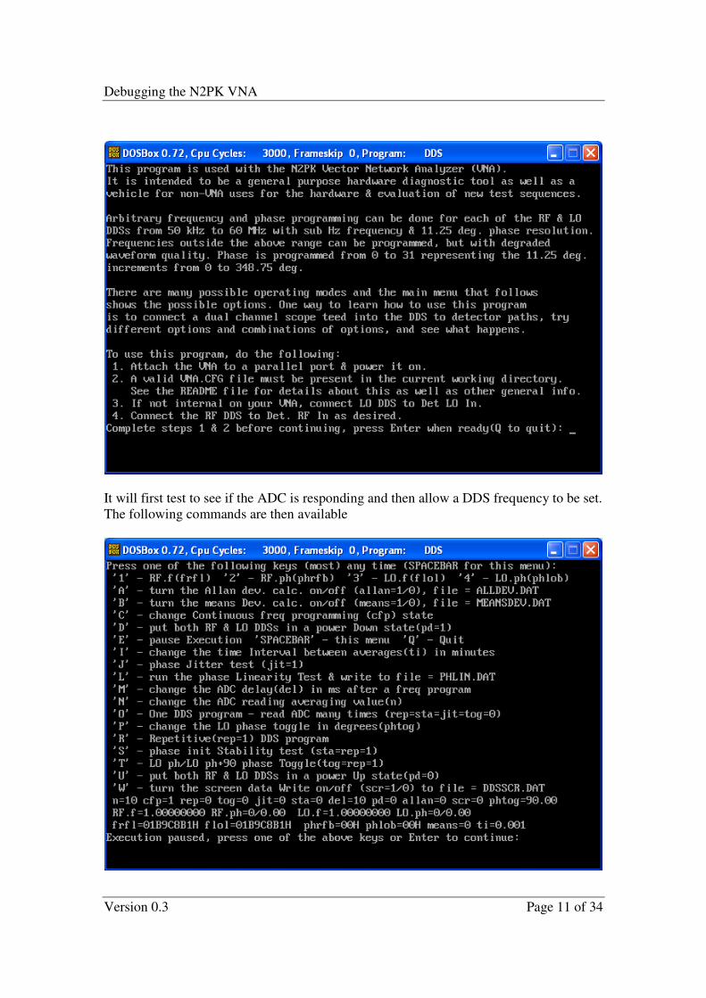
The next step after verifying basic connectivity is to test DDS setting. For this, there is
another utility called “dds.exe”. It is run in a similar manner to parport. A copy of its
instructions is shown below
Debugging the N2PK VNA
Version 0.3 Page 11 of 34
It will first test to see if the ADC is responding and then allow a DDS frequency to be set.
The following commands are then available
Debugging the N2PK VNA
Version 0.3 Page 12 of 34
At this stage the important question to answer is whether the DDSes can both be set to a
given clock and phase – try setting to 1 MHz with a 90 degree phase difference and
verify on a 2 channel oscilloscope.
Finally the program adc.exe permits continuous reading of the ADC.
3.4.1 The lowest level possible
If this fails, there is a more fundamental way to debug the hardware; use “debug”. Note
that this ONLY works for pure DOS and not DOS under windows. If all else fails boot
the PC from MS-DOS and at the command prompt enter the command “debug”. Once
here there are two commands, one reads from a port and one writes. To read from port
address 0x0378, enter the command “I 0378” followed by return. To output value 55 to
port 378, enter the command “O 378 55” followed by return. In this way, at the lowest
level possible on a PC, the lines of the parallel port may be set or cleared. If this still does
not work, and you are certain that the port addresses are right, it looks like a fault in the
hardware.
Referring to Table 1- Parallel port assignments, the two columns give the port base
address offset and bit number for a specific line. The address for a specific line is
therefore the port address plus the port offset.
3.5 Windows
To debug the parallel port from Windows there are several possibilities. There are two
issues here, the communications itself and persuading Windows to let you communicate.
First, what software will you be using? If you want to run Paul’s software, you will need
a suitable package to allow DOS programs to communicate with the hardware. Once this
is installed and working, then use Paul’s test programs as per Section 3.4 “DOS”. In fact,
Paul’s programs will also be needed to check if Windows has deigned to allow access.
First then you need to choose a package
There are several that have been successfully used; these include
• DOSbox
• Direct/IO
• UserPort
The following text refers mainly to DOSbox. If you have text to supply for the others,
please let me know.
If however you will be using a GUI program under windows such as VNA4win. myVNA
or Exeter, then proceed to section 3.5.3.
Debugging the N2PK VNA
Version 0.3 Page 13 of 34
3.5.1 DOSbox
DOSbox is an Open Source project released under the GPL. It provides a DOS runtime
environment within Windows. Whilst it does not specifically provide raw parallel port
access, there is a freely available modified version that does. Details on how to install it
were given by Steve K8JQ in message #3162 of the N2PK VNA Yahoo group. A
shortened summary is presented below.
1. From the SourceForge website ( via http://www.dosbox.com ) download version
0.72 of DOSbox and install it
2. Download the file http://home.arcor.de/h-a-l-9000/dosbox_files/directlpt7_exe.zip
which is a modified version of the DOSbox files (there are two files in the ZIP).
Replace the files of the same name in the DOSbox installation directory with the
version in the downloaded ZIP.
3. Steve’s notes indicate that it was also necessary to install PortTalk. I found that
DOSbox as modified by step 2 above did not need this on my system but if it still
does not work, follow Steve’s additional guidance as per the posting.
4. Install Paul’s utilities in a suitable directory such as c:\n2pk\tools
5. Run DOSbox and mount the directory where the tools are installed by typing the
command “mount c c:\n2pk\tools” and change directory to the c drive.
6. Execute the program and proceed with the instructions in section 3.4 “DOS”. The
aim initially is to verify that Windows is allowing access to the parallel port by
determining that it is possible to toggle one of the output lines using Paul’s
program.
7. If this cannot be done having followed the instructions given, then the problem
may lie in the installation and configuration of DOSbox or with the hardware.
8. To check if it is windows or hardware, first try a DOS boot. Insert a blank floppy
disk into the disk drive and format it from Windows, specifying that you want to
create an MS-DOS startup disk as shown here
Debugging the N2PK VNA
Version 0.3 Page 14 of 34
Copy onto the disk parport and vna.cfg and follow the instructions in Section 3.4.
9. If the problem lies in DOSbox no specific other guidance is offered here.
3.5.2 Direct I/O
For Direct I/O, see http://www.direct-io.com/
A procedure for UserPort install is available at
http://www.writelog.com/support/lpt_port_support_on_windows_nt.htm
3.5.3 Debugging Parallel Ports with myVNA
Please forgive the partisan nature of this section but I’m familiar with myVNA.
myVNA uses a package called inpout32 to bypass windows and provide access to the
hardware. The drivers are installed automatically when installing the program. Note
however that if Vista 32 or 64 are being used, you must run the installer that is also
present in the myVNA installation directory first.
Debugging the N2PK VNA
Version 0.3 Page 15 of 34
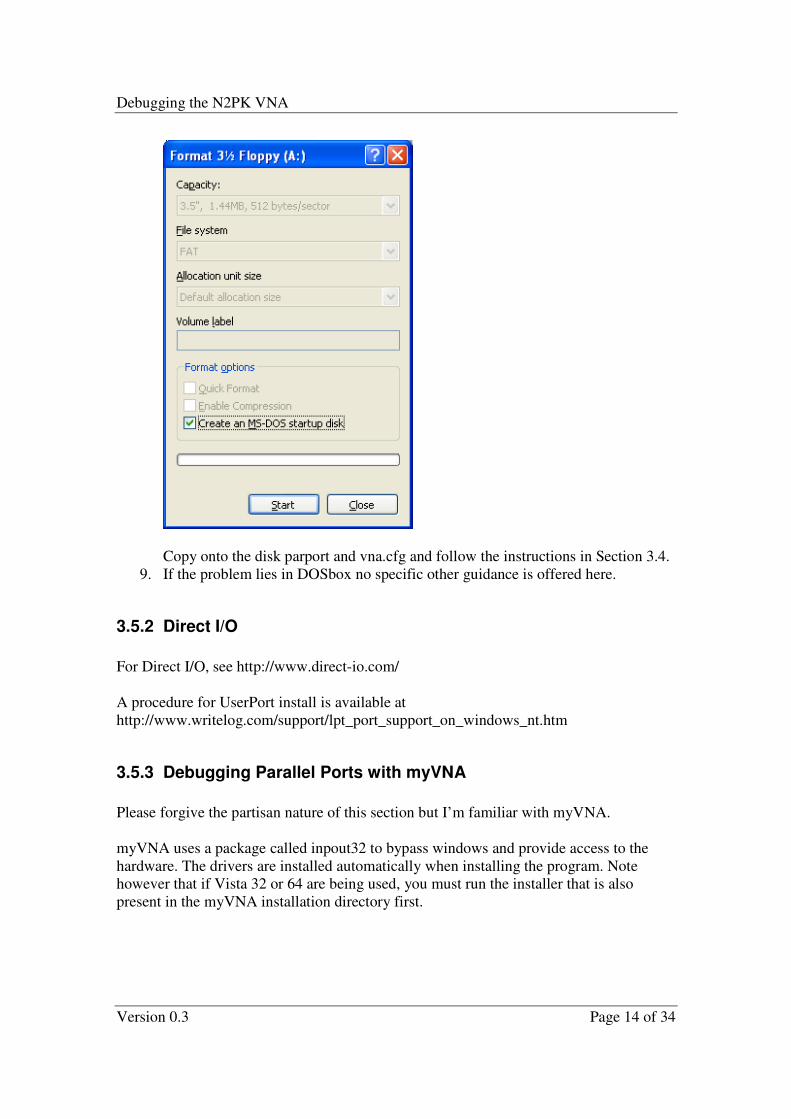
Run myVNA and follow the initial part of the Quick Start guide (which will have been
installed as part of the package) as far as setting the hardware, and specifically the
parallel port, address and port name.
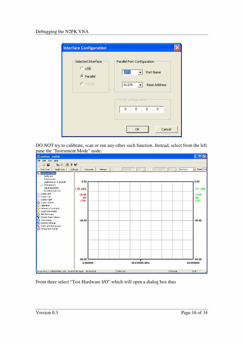
The Hardware details are accessed from the hardware node as shown below
The parallel port address must be the one determined from Section 3.2 and the port name
from Section 3.3.
Debugging the N2PK VNA
Version 0.3 Page 16 of 34
DO NOT try to calibrate, scan or run any other such function. Instead, select from the left
pane the “Instrument Mode” node.
From there select “Test Hardware I/O” which will open a dialog box thus
Debugging the N2PK VNA
Version 0.3 Page 17 of 34
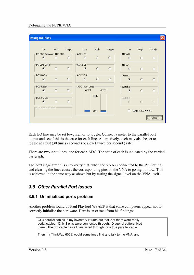
Each I/O line may be set low, high or to toggle. Connect a meter to the parallel port
output and see if this is the case for each line. Alternatively, each may also be set to
toggle at a fast (30 times / second ) or slow ( twice per second ) rate.
There are two input lines, one for each ADC. The state of each is indicated by the vertical
bar graph.
The next stage after this is to verify that, when the VNA is connected to the PC, setting
and clearing the lines causes the corresponding pins on the VNA to go high or low. This
is achieved in the same way as above but by testing the signal level on the VNA itself
3.6 Other Parallel Port Issues
3.6.1 Uninitialised ports problem
Another problem found by Paul Playford W8AEF is that some computers appear not to
correctly initialise the hardware. Here is an extract from his findings:
Of 3 parallel cables in my inventory it turns out that 2 of them were really serial cables. Only 8 pins were connected through. Diagonal cutters fixed them. The 3rd cable has all pins wired through for a true parallel cable. Then my ThinkPad 600E would sometimes find and talk to the VNA, and
Debugging the N2PK VNA
Version 0.3 Page 18 of 34
sometimes not. Turns out the LPT is not always initialized under WinDOZ XP PRO. My work-around is to install a fictitious printer (generic-text only) on LPT1 and then print a test page. The test page goes nowhere but then the software does see the VNA. Kind of a pita because I have to print the test page everytime I reboot the computer.
3.6.2 Glitches in Operation
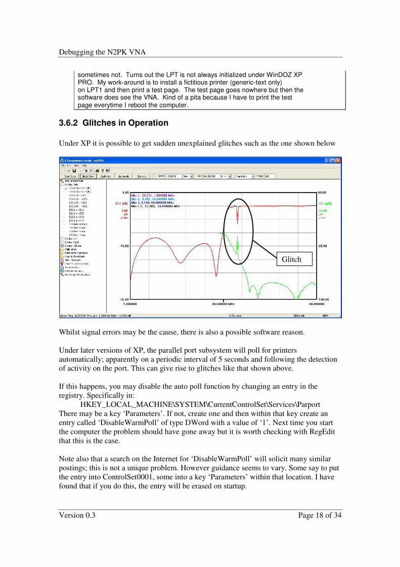
Under XP it is possible to get sudden unexplained glitches such as the one shown below
Whilst signal errors may be the cause, there is also a possible software reason.
Under later versions of XP, the parallel port subsystem will poll for printers
automatically; apparently on a periodic interval of 5 seconds and following the detection
of activity on the port. This can give rise to glitches like that shown above.
If this happens, you may disable the auto poll function by changing an entry in the
registry. Specifically in:
HKEY_LOCAL_MACHINE\SYSTEM\CurrentControlSet\Services\Parport
There may be a key ‘Parameters’. If not, create one and then within that key create an
entry called ‘DisableWarmPoll’ of type DWord with a value of ‘1’. Next time you start
the computer the problem should have gone away but it is worth checking with RegEdit
that this is the case.
Note also that a search on the Internet for ‘DisableWarmPoll’ will solicit many similar
postings; this is not a unique problem. However guidance seems to vary. Some say to put
the entry into ControlSet0001, some into a key ‘Parameters’ within that location. I have
found that if you do this, the entry will be erased on startup.
Glitch

Debugging the N2PK VNA
Version 0.3 Page 19 of 34
Do re-enable the warm polling, set the value to ‘0’.
To do this automatically, create a couple of text files called ‘EnableWarmPoll.reg’ and
‘DisableWarmPoll.reg’ with settings of 0 and 1 respectively. The contents of the files
would be as shown below. Note that if you use myVNA (versions later than 0.39) these
files will be created for you in a subdirectory called “Parallel Port Configuration” in the
program installation directory.
For DisableWarmPoll.reg:
Windows Registry Editor Version 5.00
[HKEY_LOCAL_MACHINE\SYSTEM\CurrentControlSet\Services\Parport\para
meters]
"DisableWarmPoll"=dword:00000001
And for EnableWarmPoll.reg:
Windows Registry Editor Version 5.00
[HKEY_LOCAL_MACHINE\SYSTEM\CurrentControlSet\Services\Parport\para
meters]
"DisableWarmPoll"=dword:00000000
Double click on the file. Two confirmation dialogs will be displayed, one to check you
want to modify the registry and one to confirm the change.
If you find this does not work or that the key needs to be elsewhere to work on your
system, please let me know.
3.6.3 Port Type
This does not quite make sense to me, but Roderick reports that the final resolution to his
problem was that the parallel port was not set to a “bidirectional port”. The reason this
does not make sense is that the N2PK VNA hardware does not make use of bidirectional
communications on the data lines. Nevertheless, it solved his problem. Note that the
BIOS may show the parallel port type in many different ways. The most common types
are as shown below. It should not matter but if you cannot see the output lines changing,
try changing the port type in the BIOS
SPP Standard Parallel Port
EPP Enhanced Parallel Port (i.e. bidirectional)
ECP Enhanced Communication Port (has FIFOs and support for faster
data transfer modes)
Debugging the N2PK VNA
Version 0.3 Page 20 of 34
ECP + EPP Both ECP and EPP
3.7 Other Operating Systems
My knowledge of Linux and MACs is poor. This section hopefully will grow with time
and the expertise of others. Here is some advice from Gary Johnson:
Macintosh users currently need to run Windows under BootCamp or virtualization
software such as Parallels Desktop or VMWare Fusion. All of these options require an
Intel-based Macintosh and a legal copy of Windows, typically XP SP2 or Vista. The
other important thing to note is that you must use the USB interface to the VNA since
there is no way to add a parallel port to a Macintosh (USB parallel port adapters don't
work, either). Once you have your copy of Windows running, your can follow the
directions in this document exactly as if you were using any other regular PC.
Performance under BootCamp is exactly the same as any PC, and there is only a modest
speed penalty when running in a virtual environment.
Linux users can also use VMWare with Windows in the same manner. It may be possible
to access the parallel port, if you have one, but this has not been tested.
Another multi-platform possibility is an implementation of Wine for Macintosh or Linux,
such as Crossover from Codeweavers. Wine is an environment that implements a clone of
the Windows API (application programming interface) in such a way that the entire
Windows OS is not needed. However, it is very unlikely that it will be possible to install
the required USB DLL to talk to the VNA, so we'll recommend you take another
approach.
4 USB port
The USB port assumed here is the G8KBB design either using one of Dave’s original
boards, the commercial Elrasoft module or one of the near clones such as Dave
WB6DHW’s HSUSB). Functionally all these are the same. There are slight hardware
differences as below.
4.1 Hardware issues
Physical connections. The Elrasoft and G8KBB modules use a 40 pin DIL connector to
connect to the VNA. The WB6DHW deisign uses a set of connectors, but the only ones
we are interested in are H3 and H4. These connect to the VNA as shown below.
The Elrasoft and G8KBB boards use a Type B USB connector and a standard USB cable.
The WB6DHW unit uses a mini USB Type B connector. Cited as “the type used on
Debugging the N2PK VNA
Version 0.3 Page 21 of 34
digital cameras” some care must be exercised as a number of camera manufacturers
implement non standard cables with the form factor of a mini USB connector. Make sure
the cable is correct.
Also note that the USB interface is based on a USB 2.0 controller and, if plugged in to a
USB 2.0 port, will run at the hi speed data rate – 480 Mbit/s. Do not use poor quality or
low speed cables and – most definitely – do not use USB extender cables.
The USB interfaces are bus powered. Do not apply 5V externally.
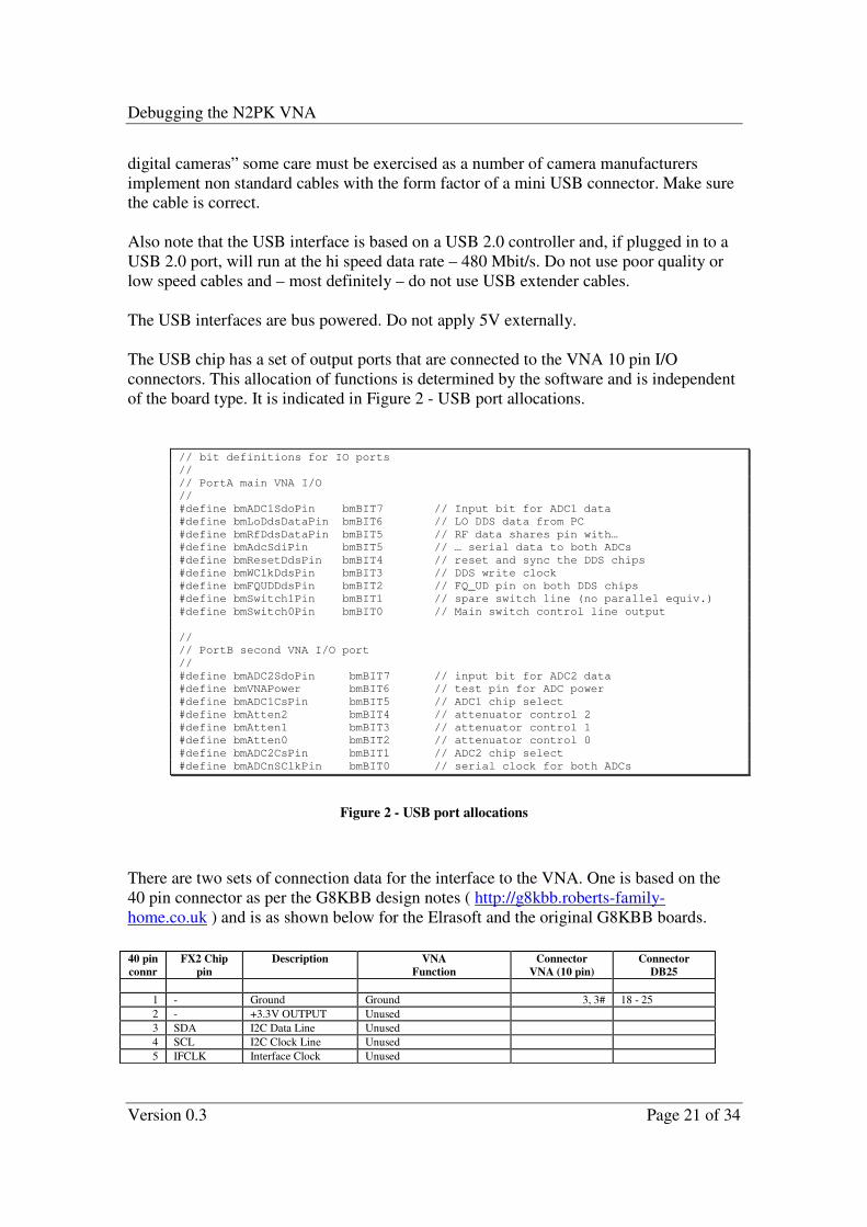
The USB chip has a set of output ports that are connected to the VNA 10 pin I/O
connectors. This allocation of functions is determined by the software and is independent
of the board type. It is indicated in Figure 2 - USB port allocations.
// bit definitions for IO ports
//
// PortA main VNA I/O
//
#define bmADC1SdoPin bmBIT7 // Input bit for ADC1 data
#define bmLoDdsDataPin bmBIT6 // LO DDS data from PC
#define bmRfDdsDataPin bmBIT5 // RF data shares pin with…
#define bmAdcSdiPin bmBIT5 // … serial data to both ADCs
#define bmResetDdsPin bmBIT4 // reset and sync the DDS chips
#define bmWClkDdsPin bmBIT3 // DDS write clock
#define bmFQUDDdsPin bmBIT2 // FQ_UD pin on both DDS chips
#define bmSwitch1Pin bmBIT1 // spare switch line (no parallel equiv.)
#define bmSwitch0Pin bmBIT0 // Main switch control line output
//
// PortB second VNA I/O port
//
#define bmADC2SdoPin bmBIT7 // input bit for ADC2 data
#define bmVNAPower bmBIT6 // test pin for ADC power
#define bmADC1CsPin bmBIT5 // ADC1 chip select
#define bmAtten2 bmBIT4 // attenuator control 2
#define bmAtten1 bmBIT3 // attenuator control 1
#define bmAtten0 bmBIT2 // attenuator control 0
#define bmADC2CsPin bmBIT1 // ADC2 chip select
#define bmADCnSClkPin bmBIT0 // serial clock for both ADCs
Figure 2 - USB port allocations
There are two sets of connection data for the interface to the VNA. One is based on the
40 pin connector as per the G8KBB design notes ( http://g8kbb.roberts-family-
home.co.uk ) and is as shown below for the Elrasoft and the original G8KBB boards.
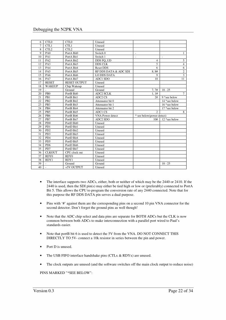
40 pin FX2 Chip Description VNA Connector Connector
connr pin Function VNA (10 pin) DB25
1 - Ground Ground 3, 3# 18 - 25
2 - +3.3V OUTPUT Unused
3 SDA I2C Data Line Unused
4 SCL I2C Clock Line Unused
5 IFCLK Interface Clock Unused
Debugging the N2PK VNA
Version 0.3 Page 22 of 34
• The interface supports two ADCs, either, both or neither of which may be the 2440 or 2410. If the
2440 is used, then the SDI pin(s) may either be tied high or low or (preferably) connected to PortA
Bit 5. This allows the CPU to program the conversion rate of any 2440 connected. Note that for
this purpose the RF DDS DATA pin serves a dual purpose.
• Pins with ‘#’ against them are the corresponding pins on a second 10 pin VNA connector for the
second detector. Don’t forget the ground pins as well though!
• Note that the ADC chip select and data pins are separate for BOTH ADCs but the CLK is now
common between both ADCs to make interconnection with a parallel port wired to Paul’s
standards easier.
• Note that portB bit 6 is used to detect the 5V from the VNA. DO NOT CONNECT THIS
DIRECTLY TO 5V- connect a 10k resistor in series between the pin and power.
• Port D is unused.
• The USB FIFO interface handshake pins (CTLx & RDYx) are unused.
• The clock outputs are unused (and the software switches off the main clock output to reduce noise)
PINS MARKED "*SEE BELOW":
6 CTL0 CTL0 Unused
7 CTL1 CTL1 Unused
8 CTL2 CTL2 Unused
9 PA0 PortA Bit0 Switch 0 - 1
10 PA1 PortA Bit1 Switch 1 - -
11 PA2 PortA Bit2 DDS FQ_UD 4 5
12 PA3 PortA Bit3 DDS CLK 5 4
13 PA4 PortA Bit4 Reset DDS 6 6
14 PA5 PortA Bit5 RF DDS DATA & ADC SDI 8, 8# 2
15 PA6 PortA Bit6 LO DDS DATA 9 3
16 PA7 PortA Bit7 ADC1 SDO 10 11
17 RESET RESET OUTPUT Unused
18 WAKEUP Chip Wakeup Unused
19 - Ground Ground 7, 7# 18 - 25
20 PB0 PortB Bit0 ADC2 SCLK 1, 1# 7
21 PB1 PortB Bit1 ADC2 CS 2# 9 *see below
22 PB2 PortB Bit2 Attenuator bit 0 14 *see below
23 PB3 PortB Bit3 Attenuator bit 1 16 *see below
24 PB4 PortB Bit4 Attenuator bit 2 17 *see below
25 PB5 PortB Bit5 ADC1 CS 2 8
26 PB6 PortB Bit6 VNA Power detect * see below(power detect)
27 PB7 PortB Bit7 ADC2 SDO 10# 12 *see below
28 PD0 PortD Bit0 Unused
29 PD1 PortD Bit1 Unused
30 PD2 PortD Bit2 Unused
31 PD3 PortD Bit3 Unused
32 PD4 PortD Bit4 Unused
33 PD5 PortD Bit5 Unused
34 PD6 PortD Bit6 Unused
35 PD7 PortD Bit7 Unused
36 CLKOUT CPU clock out Unused
37 RDY0 RDY0 Unused
38 RDY1 RDY1 Unused
39 - Ground Ground 18 - 25
40 - +5V OUTPUT Unused
Debugging the N2PK VNA
Version 0.3 Page 23 of 34
• Apart from the ADC power detect function, these pins are used only for the second ADC &
extended functions in Paul's documentation and are provisional (as Paul may change them yet).
Table 2 - connecting G8KBB & Elrasoft boards to VNA
The second is as used for the WB6DHW card.
J160 DB25 PORT FUNCTION H2 H3
1 7 PB0 DET1 2 SCK 2
2 8 PB5 DET1 Ncs 12
3 G,22
4 5 PA2 DDS FQ_UD 11
5 4 PA3 DDS W_CLK 9
6 6 PA4 DDS RESET 7
7 G,23
8 2 PA5 RF DDS DATA, DET1 2 SDI 5
9 3 PA6 LO DDS DATA 3
10 11 PA7 DET1 nSDO 1
J360
1 7 PB0 DET1 2 SCK 2
2 9 PB1 DET2 nCS 4
3 G,19
4 X
5 X
6 X
7 G,20
8 2 PA5 RF DDS DATA, DET1 2 SDI 5
9 X
10 12 PB7 DET2 nSDO 16
1 PA0 TEST SET SW 15
14 PB2 ATTEN0 6
16 PB3 ATTEN1 8
17 PB4 ATTEN2 10
+5 thru 10K ohms PB6 VNA PWR 14
Note that ideally PB6 is connected via 10K resistor to the 5V output of the VNA. If you cannot do
this then connect it to 5V locally on the PCB.
Note also that the WB6DHW board puts an RC combination on the Wakeup pin of the chip. I
cannot guarantee that I won’t use this pin in the future for another purpose so note that ideally you
should not populate these components, but if you have already assembled them do not bother to
remove them. Their presence and the difference to the original board is not an error and not a
possible reason for having difficulties in getting the interface to work.
Finally note also that the voltage rating of the R and C connecting screen and ground on the USB
connector are not adequately rated for safety but again the difference here does not represent a
reason for having problems with the board.
Table 3 - Connecting the WB6DHW board
Debugging the N2PK VNA
Version 0.3 Page 24 of 34
4.2 USB Configuration
For initial testing, disconnect the USB interface from the VNA.
The first stage of testing is to ensure that the USB device is working correctly. There are
several stages to this.
Plug the interface into a Windows computer. The “Found new hardware” wizard should
appear (give it a couple of minutes). DO NOT allow the wizard to proceed at this stage.
The specific details on how to install the drivers are given in the USB Interface Board
documentation available from http://g8kbb-roberts-family-home.co.uk and specifically
the chapter “USB Configure”. To understand what is going on, it is important to
understand how the interface works.
When powered up, the USB interface chip reads its eeprom for either code or an
identifier. If it finds code, it boots that code immediately. Otherwise it reads the identifier
alone. This is the mode we use for the VNA. The chip then identifies itself on the USB
bus using this identifier.
Windows, whenever it sees a device, uses its identifier to locate the drivers it needs.
When you plug in the brand new device, its EEPROM is blank. This is a special situation
that the USB chip recognises and it uses a Cypress default identifier. That identifier read
by Windows and it goes looking for a driver for it. Chances are it will not find it but there
is a chance that it may from the online services of Microsoft, so DO NOT LET IT. When
you installed USB Configure, two sets of drivers will have been installed. One is the
drivers for this “blank eeprom” state and the other is for the device working on a VNA
interface.
An identifier by the way comprises three things, a Vendor ID (VID) a Product ID (PID)
and a BCD Identifier.
Ok, so you have installed USB Configure. The initial hardware wizard is looking for the
drivers for a device with a blank EEPROM. You install those drivers as per the
documentation. Now windows knows a little bit about the interface – it knows how to
talk to it using a driver called “ezusb.sys” and each time you plug it in it will get that far.
Now however we want it to work as a VNA interface, and it needs an identifier for that.
To do this we need to program the EEPROM with a unique ID. That is what USB
configure does. Follow its instructions and program the chip. Now, whenever you plug in
the interface it will identify itself with this new ID. At this point the n2pkvld.sys driver
will be run by windows. This driver downloads to the RAM of the USB controller the
interface program for the VNA and then causes the chip to reset itself. When it does that
it appears to Windows as a new device with yet another ID. This time it appears aVNA
interface and is ready to use.
Debugging the N2PK VNA
Version 0.3 Page 25 of 34
Why this complexity? It means that the code running on the USB controller chip is easily
changeable as new versions are released.
So, what does this mean for debugging? USBview is your first port of call. Use it to
check the VID and PID of the device. You are looking to see that it arrives at the end
state as above. Until it does, correctly, each time you plug it in, you will get no further
with it. Remember that USBview needs to be refreshed (via the menu) or it will not
update its display. Unfortunately given the complexity of Windows no specific guidance
is easy to give at this point.
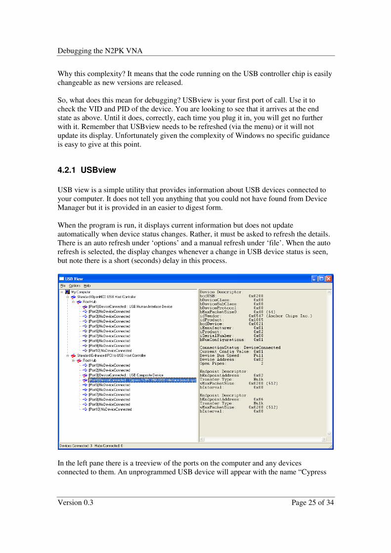
4.2.1 USBview
USB view is a simple utility that provides information about USB devices connected to
your computer. It does not tell you anything that you could not have found from Device
Manager but it is provided in an easier to digest form.
When the program is run, it displays current information but does not update
automatically when device status changes. Rather, it must be asked to refresh the details.
There is an auto refresh under ‘options’ and a manual refresh under ‘file’. When the auto
refresh is selected, the display changes whenever a change in USB device status is seen,
but note there is a short (seconds) delay in this process.
In the left pane there is a treeview of the ports on the computer and any devices
connected to them. An unprogrammed USB device will appear with the name “Cypress
Debugging the N2PK VNA
Version 0.3 Page 26 of 34
EZ-USB FX2 (68613) - EEPROM missing”. A device that has been programmed but
failed the bootstrapping process that loads its code will appear with the name “Using
N2PKvna.inf for EZ-Loader before ReNumeration (n2pkvld.sys)” and a fully working
interface will have the name “Cypress N2PK VNA USB Interface (ezusb.sys)”
On the right pane is the details for a device. Selecting a device displays specific
information for it.
For the various states of the interface the following values will be seen
idVendor idProduct
Uprogrammed eeprom 0x04B4 0x8613
VNA with programmed EEPROM but no
drivers found
0x0547 0x1004
VNA correctly booted 0x0547 0x1005
In the case of the correctly booted device, the bcdDevice value is the firmware release
number. This should be at least 19 (i.e. build 0.19) for correct operation and preferably
should be build 21.
Note that the interface is cheekily abusing the Cypress Vendor ID and it is possible that
another device uses the same ID. If this happens contact Dave G8KBB.
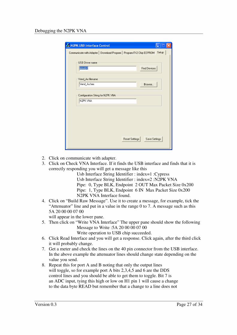
4.2.2 USB Configure
USBConfigure has two purposes. The first is to program the EEPROM. The second is to
check the correct operation of the interface. Programming is addressed in the
USBConfigure documentation. This section will deal with debugging
1. Select the setup tab, click “find devices” and make sure it has found the interface.
It may find more than one if you have multiple VNAs. If not and more than one
appear to exist then Windows is confused, possibly by rapid connection and
disconnection from USB ports
Debugging the N2PK VNA
Version 0.3 Page 27 of 34
2. Click on communicate with adapter.
3. Click on Check VNA Interface. If it finds the USB interface and finds that it is
correctly responding you will get a message like this
Usb Interface String Identifier : index=1 :Cypress
Usb Interface String Identifier : index=2 :N2PK VNA
Pipe: 0, Type BLK, Endpoint 2 OUT Max Packet Size 0x200
Pipe: 1, Type BLK, Endpoint 6 IN Max Packet Size 0x200
N2PK VNA Interface found.
4. Click on “Build Raw Message”. Use it to create a message, for example, tick the
“Attenuator” line and put in a value in the range 0 to 7. A message such as this
5A 20 00 00 07 00
will appear in the lower pane.
5. Then click on “Write VNA Interface” The upper pane should show the following
Message to Write :5A 20 00 00 07 00
Write operation to USB chip succeeded.
6. Click Read Interface and you will get a response. Click again, after the third click
it will probably change.
7. Get a meter and check the lines on the 40 pin connector from the USB interface.
In the above example the attenuator lines should change state depending on the
value you send.
8. Repeat this for port A and B noting that only the output lines
will toggle, so for example port A bits 2,3,4,5 and 6 are the DDS
control lines and you should be able to get them to toggle. Bit 7 is
an ADC input, tying this high or low on H1 pin 1 will cause a change
to the data byte READ but remember that a change to a line does not
Debugging the N2PK VNA
Version 0.3 Page 28 of 34
appear in the read data until the third time you read due to internal
doubble buffering.
9. Check the ADC lines and inputs in the same way
10. Once you are satisfied that the interface works, try the "Build
Set Message" command. Put a scope on the DDS lines but note that what
is about to happen is about to happen very quickly so a storage scope
would be better. Tick the "set dds" option and enter a frequency for
LO and RF of something that toggles, for example 0x5555555555.
Connect scope to DDS lines (or a logic analyser) and execute the
command with the "write VNA interface" button. You will get a series
of very fast pulses as the chip tries to set the DDS. If you do not
have a storage scope or logic analyser, then you can achieve a
similar repetitive effect using myVNA and the sweep function. Go to
instrument mode, signal generator, select the sweep option, give it a
couple of frequencies to sweep from, set the step delay to 100 usec,
the number of steps to 1000 and click start. You should then see a
continuous series of pulses on the DDS control lines. Compare this
with the diagrams in the myVNA quickstart guide or the more detailed
traces here
http://g8kbb.roberts-family-home.co.uk/USB_Interface_Timings.doc
11. Once you are satisfied that the interface is working, connect it
to the VNA. Repeat step 6 and trace the lines to the DDS chips. Check
the DDS output, it should be sweeping.
4.3 Upgrading drivers
To upgrade the drivers follow the instructions in http://g8kbb-roberts-family-home.co.uk
and note that you should preferably be using version 0.21 or later.
4.4 Windows
Debugging starts with USB Configure. First check that the board has been found, and that
it is correctly working. Check that the drivers have been loaded and that it is recognised
as a VNA interface. Use USBconfigure to program the eeprom.
If you have any problems with drivers, and have loaded any of the Cypress tools such as
CyConsole, uninstall all such software and drivers. Now try again with the drivers.
To test the IO lines, follow the guidance in section 3.5.3 but from the hardware, select
USB as shown below
Debugging the N2PK VNA
Version 0.3 Page 29 of 34
Also note that in USB mode there is an additional input line – VNA power – the status of
which is shown in the bottom left of the display
Once you are confident of this try running a program such as VNA4win, Exeter or
myVNA. Start with a simple function such as setting or clearing attenuator or switch
lines, then move on to the program’s signal generator mode and check that. Finally try
Debugging the N2PK VNA
Version 0.3 Page 30 of 34
the ADC reading modes of the program. Having done all this try the sweep functions.
Details on the individual application programs is given below.
4.5 Other Operating Systems
Caveat Emptor. I have neither a MAC nor Linux. Sorry.
5 Paul’s Programs
Paul’s programs are all DOS executables. Running on XP, Windows 2000 or Vista will
require suitable access to the hardware bypassing the OS. There are many posts on the
Yahoo group on this as noted previously in section 3.5.
Note that, in all cases, a valid vna.cfg file needs to be present and must correctly specify
the VNA details.
In each case, the programs give full operating instructions from the front page. The test
sequence is first to use Parport.exe, dds.exe and adc.exe to test the low level hardware
and comms then use one of the main application programs. The current set of programs
include executables for:
• Transmission
• Reflection
• Dual Detector scans
• Crystal measurements
• Harmonic mode scans
• S parameter scans
• RFChk. - RF Check verifies the DDS level and DDS and detector return losses
and impedances.
• Debug programs
To obtain the latest software, go to Paul’s homepage http://n2pk.com
6 myVNA
So have you read the quickstart guide? If not go read up to and including the section on
“scanning”.
Assuming you have, debug the port you are using as described above.
Check that the “Hardware” settings are OK then, from “Instrument Mode” select “Signal
Generator”.
Debugging the N2PK VNA
Version 0.3 Page 31 of 34
Select “Fixed Frequency” and “LO locked to RF” and enter a suitable frequency. Click
“Set” and check the output frequency. If OK, untick “LO locked to RF”, enter a different
frequency for LO as RF and check that both can be set. If the DDS cannot be set, go back
to the port debugging sections presented earlier.
Once satisfied that setting DDS works, tick the ADC1 box and click on “Start”. A
changing ADC voltage and a progress bar that represents the voltage should be shown
bottom left.
Having done this, try a sweep.
7 VNA4win
OK, have you read the VNA4win manual? If not and you are having problems, go get a
copy of it. It is preferable that you read it but if you won’t, then read the sections on
“Installation”, “Quick Tour” and “Configuring VNA.INI” as a minimum. Then go to the
section on “Manual Control”. The Manual Control function provides a low level debug
facility to set the DDS and read the ADC. If you are using USB or Parallel, go to the
previous section on parallel or USB debugging and configuration as appropriate for initial
diagnostics if the set DDS and ADC read functions do not work.

Debugging the N2PK VNA
Version 0.3 Page 32 of 34
Once you are satisfying that the program is correctly setting the DDS to a specified
frequency and that you are getting an ADC reading, return to “Quick Tour” and try a
sweep.
If you have problems however, you need to solve them before proceeding.
If the problem is that the frequency is slightly off, you must set the Clock Frequency in
vna.ini.
If the DDS are not set correctly, go check the hardware first.
If you are using USB check that the line “usb = yes” is present in vna.ini. If you are using
the parallel port make sure it is not present (or ic commented out by preceding with a “ ‘
“.
For parallel output, VNA4win uses inpout32.dll. If you are having problems, check the
version and, if using Vista64, be aware that you may need to upgrade to a compatible
version.
For USB output, VNA4win uses vnadll.dll. To debug it, use USBConfigure as described
previously.
Debugging the N2PK VNA
Version 0.3 Page 33 of 34
8 Exeter
Exeter either uses the parallel port via VNAccess.dll and a package such as UserPort to
bypass windows or it uses the USB interface. To implement the USB interface, go to the
website http://g8kbb.roberts-family-home.co.uk and follow the links to Exeter. This
describes how to replace VNAccess.dll with a USB version.
Exeter possesses a signal generator function that may be used to test the hardware; it may
be better to use myVNA or USBconfigure initially for low level testing.
The signal generator is accessed from the “Tools” menu and pops up a dialog box as
shown below.
Initially set the controls as shown in the example below – RF generator set to 10 MHz
and LO generator locked to it with 90 degree phase difference.
Click on “Start” and check the output of the DDSs.

Debugging the N2PK VNA
Version 0.3 Page 34 of 34
9 VNAView
Gary Johnson has produced a LabView VI for the VNA. Here are some details from him:
There is a multi-platform option, for users of National Instruments' LabVIEW. If you
have the LabVIEW Full Development System or Student Edition, you can communicate
directly with the VNA via the USB interface using NI-VISA drivers, which are included
with LabVIEW or available as a free download from www.ni.com. This works under
Windows and Linux (LabVIEW 7.0 or higher), and Intel Macintosh (LabVIEW 8.2 or
higher). It should also work for LabVIEW RT and VxWorks, if you are into hard real-
time applications. Besides NI-VISA, you also need LabVIEW VIs that handle the VNA
protocol as implemented by G8KBB in his USB interface. These LabVIEW driver VIs
and a full application (VNAView) are available free from WB9JPS, including all the
source. [FOOTNOTE For adventurous programmers, it should be noted that NI-VISA is
also accessible from any programming language, so it is in fact possible to write new
VNA applications in, for instance Java or C++, and have those compile under any OS
that is supported by NI-VISA.]
Directions on installing and configuring NI-VISA for USB devices on all platforms is
included with the NI-VISA help system. There is one possible conflict that occurs under
Windows. If you choose to have NI-VISA take over as the driver for your VNA USB
interface, it then becomes impossible for the regular G8KBB DLL-based driver to access
that device. Thus, you could not run both a LabVIEW-based application and, for
instance, myVNA or VNA4Win. You would have to disable the NI-VISA USB driver
each time you wanted to use one of those other applications. But there is an easy solution.
The VNAView driver library also includes an option to not use NI-VISA, and instead use
the DLL. This solution is a Windows-only option and was created specifically to solve
this conflict. In fact, we have run VNAView and myVNA simultaneously, as long as they
don't try to acquire data at the same time.
I believe a stand-alone executable is also in production.
### End of Document ###