current-source parallel-resonant dc/dc converter
TRANSCRIPT

IEEE TRANSACTIONS ON INDUSTRIAL ELECTRONICS, VOL. 42, NO. 2, APRIL 1995 199
Current- S ource Parallel-Resonant DCDC Converter Marian K. Kazimierczuk, Senior Member, IEEE, and Abdulkarim Abdulkarim
Abstract-This paper introduces, analyzes, and experimentally verifies a novel dddc converter called the current-source parallel- resonant converter. The converter consists of a large choke inductor, two switches, and a parallel-resonant circuit. Each switch consists of a MOSFET in series with a diode. It has a nonpulsating input current with a very low ac ripple. The MOSFET's are driven with respect to ground and, therefore, have a simple gate-drive circuit. The analysis of the converter is carried out in the frequency domain using Fourier series techniques. Analytical expressions are derived for performance parameters of the converter. A prototype of the converter circuit was designed, built, and tested. The theoretical results were in good agreement with the experimental results.
I. INTRODUCTION
OLTAGE-source multi-switch inverters employ either a series-resonant circuit or resonant circuits that are
derived from the series-resonant circuit. In voltage-source half- bridge resonant converters, one of the switches is connected in series with the dc input voltage source. Therefore, the current drawn from the dc input supply is a half sinusoid, injecting a large amount of harmonics to the front-end rectifier and to the utility line and thus causing electromagnetic pollution. In contrast, in current-source resonant converters [l], [2], the current drawn from the dc voltage supply is constant and continuous. In 1982, Kassakian introduced a current-source converter that requires two choke input inductors [l]. In 1988, Akagi et al. introduced a current-source phase-controlled full- bridge converter using static induction transistors and two totem pole legs [2].
The objectives of this paper are to: 1) introduce a current- source parallel-resonant converter, 2) present a comprehensive frequency-domain analysis of this current-source converter for steady-state operation, 3) give a design example, and 4) verify the theoretical design with experimental results.
Voltage-source converters contain one or two totem pole switching legs, in which it is difficult to drive the upper transistor(s). One of the major advantages of the current-source parallel-resonant converter is a simple gate-drive circuit. This is because the gates of both MOSFET's are referenced to ground and, therefore, the drivers do not require isolation transformers or optical couplers. In typical voltage-source series resonant converters, the output voltage of the converter increases as the frequency approaches the resonant frequency.
Manuscript received February 28, 1992; revised January 14, 1994 and October 3,1994. This work was supported by the National Science Foundation under Grant ECS-8922695.
The authors are. with the Department of Electrical Engineering, Wright State University, Dayton, OH 45435 USA.
IEEE Log Number 94088 12.
+ V W -
1
I * T
I I
(b)
(C)
Fig. 1. Current-source inverter with a parallel-resonant circuit. (a) Circuit. (b) Equivalent circuit with parasitic resistances and offset voltage sources. (c) Simplified model.
Conversely, the output voltage decreases as the frequency gets closer to the resonant frequency in the current-source parallel-resonant converter. The operation below resonance is preferred because the efficiency is much higher than that above resonance.
11. PRINCIPLE OF OPERATION
A circuit of a current-source inverter with a parallel-resonant circuit is shown in Fig. l(a). It consists of a large choke inductor L f ; , two switches SI and Sz, and an R;LC parallel- resonant circuit. The dc input source VI and the choke inductor L f i form a dc input current source Ir. R; is the input resistance of the ac load. The circuit requires unidirectional switches for the current and bidirectional switches for the voltage. Such a switch can be obtained by connecting a MOSFET in series with an ultrafast diode. The intrinsic body-drain p-n junction diode of the MOSFET is disabled by the series diode. As a
I 1 ' 1
02784046/95$04.00 0 1995 IEEE
~______

200 IEEE TRANSACTIONS ON INDUSTRIAL ELECTRONICS, VOL. 42, NO. 2, APRIL 1995
(C) Fig. 2. former center-tapped rectifier. (c) Bridge rectifier.
Class D voltage-driven rectifiers. (a) Half-wave rectifier. (b) Trans-
result, the switch can conduct only a positive current and can block either positive or negative voltage. The MOSFET's are driven by rectangular gate-to-source voltages VGSl and VGSZ
at the operating frequency f = 1/T and with an on-duty cycle of slightly greater than 50%. To provide the path for the dc input current source II, either one or both switches should be ON. Therefore, slightly overlapping gate-to-source voltages should be used. MCT's, which have blocking capabilities for both positive and negative voltages, can also be employed as switches in the inverter.
Fig. l(b) shows an equivalent circuit of the inverter with parasitic resistances and offset voltage sources, where ~ ~ f i is the series equivalent resistance (ESR) of the input inductor Lf i , TDS is the MOSFET on-resistance, TF is the diode forward resistance, V F ~ is the diode offset voltage, R L ~ is the equivalent parallel resistance (EPR) of the resonant inductor L, and RcP is the EPR of the resonant capacitor C. When switch SI is OFF and switch SZ is ON, the dc input current I1 flows into the resonant circuit and the energy is transferred from the dc input source to the resonant circuit. When Sl is ON and S2 is OFF, the dc input current II flows through switch SI and the energy stored in the resonant circuit is partially discharged into the load. Assuming that the input inductor and the switches are ideal, the circuit composed of VI, L f ; , S1, and S2 can be modeled by a square-wave current source i = isz, as shown in Fig. l(c).
If the load of the inverter is replaced by a rectifier, a dc/dc converter is obtained. Fig. 2 shows three Class D voltage- source rectifiers [3] that are compatible with the inverter shown in Fig. l(a). The parallel-resonant circuit forces a sinu- soidal voltage w ~ i . Since only the power of the fundamental
f - 1, f > f ,
(b)
Fig. 3. Waveforms in current-source inverter. (a) f < fo. (b) f = fo. (c) f fo.
component is transferred from the inverter to the rectifier, the rectifier can be represented by its input resistance R; at the operating frequency f [ 131.
The principle of operation of the current-source inverter is explained by the current and voltage waveforms, depicted in Fig. 3. Fig. 3(a)-(c) shows the waveforms for f < fo, f = f o
and f > fo, respectively, where fo = 1 / 2 7 ~ m is the resonant frequency. The input current of the resonant circuit is a square wave of magnitude II. When the switch voltage is positive and higher than the diode threshold voltage, the series diode is ON and, therefore, the MOSFET must be OFF to block the voltage. When the switch voltage is negative, the series diode is OFF and the transistor can be either ON or OFF because the diode can block the switch voltage. For this reason, the duty cycle Dt of the MOSFET should be greater than or equal to the duty cycle of the entire switch D. Thus, the range of Dt is D 5 Dt 5 Qmax), as indicated by the cross-hatched areas in Fig. 3(a) and (c).
For f < fo, the parallel-resonant circuit represents an inductive load. Therefore, the voltage across the resonant circuit VR; leads the fundamental component iil of the current through the resonant circuit i by the phase angle The switch begins the off-state with a positive voltage and ends with a negative voltage. Let us consider the operation of switch SI. Prior to w t = 0, switch SI is ON, its current is II, and its voltage is approximately zero. At w t = 0, voltage VGSl is reduced from high to low and the MOSFET Q1 is turned off. During the interval 0 < w t 5 7r, voltage ws1 is positive, diode DQ, is ON, and transistor Q1 must be OFF to support the switch voltage. When the switch voltage increases, the diode conducts a small current that charges the transistor output capacitance. Thus, the voltage across the series diode DQ, is 0.7 V and the switch voltage across transistor Q1 is equal to wsl-0.7 V. When wsl is decreased below 0.7 V, the series diode Dol is turned off and transistor Q1 can be
7- ~~ I ' I I

KAZIMIERCZUK AND ABDULKARIM: CURRENT-SOURCE PARALLELRESONANT DC/DC CONVERTER
~
201
either ON or OFF. The diode tums off at low du/dt and at zero d i ld t . The derivative dw/dt is limited by the sinusoidal voltage across the parallel-resonant circuit. The MOSFET prevents the current flow prior to diode turn-off. Consequently, the turn- off switching loss in the diode is zero. The diode supports the switch voltage, when the switch voltage is negative, if the transistor is ON. If the transistor is OFF, both the diode and the transistor block the switch voltage. At wt = T , voltage UGSZ is reduced from a high to a low level and transistor Q2 is tumed off. At this time, the inductor current II causes the series diode DQ, to tum on. During the interval T < wt 5 2 ~ , Q1 is already ON and, therefore, switch S1 is tumed on and stays ON until the beginning of the next period. When the switch voltage increases, the MOSFET output capacitance Cout is charged via diode DQ, to the peak value of the switch voltage VSM = V, and then remains at that voltage until the transistor tums on. At this time, the capacitance Cout is discharged through the transistor, resulting in a tum-on switching loss in the MOSFET PO M fC,,utV$M/2. Only the turn-off transition of the switch is directly controllable by the driver. The turn- on switch transition is caused by the turn-off transition of the other switch.
For f = f o , the parallel-resonant circuit represents a purely resistive load and, therefore, the current iil and voltage W R ~ are in phase, as shown in Fig. 3(b). In this case, the MOSFET's tum on and off at zero voltage, resulting in zero-voltage switching, zero switching losses, and high efficiency. Since the switch voltages are never negative, the series diodes are not required and can be removed, reducing conduction losses.
For f > f,, the parallel-resonant circuit represents a capacitive load. Hence, the voltage across the resonant circuit W R ~ lags behind the fundamental component i;l of the current i by the phase angle $. The switch begins the off-state with a negative voltage and ends with a positive voltage. Let us consider the operation of switch S I . Prior to wt = 0, switch S1 is ON, its current is I I , and its voltage is approximately zero. At wt = 0, voltage VGSZ is increased from a low to a high level and the MOSFET QZ is tumed on. As a result, the dc input current I I is diverted from switch S1 to switch Sa, which causes the series diode DQ, to tum off. Diode D Q ~ tums off at high d i l d t , causing a reverse-recovery switching loss. When the switch voltage ws1 is negative, the series diode DQ, is OFF and the MOSFET Q1 can be either ON or OFF. Transistor Q1 must be tumed off when the voltage wsl is negative as indicated by the shaded area shown in Fig. 3(c). As the switch voltage wsl crosses zero, diode DQ, tums on at low dw/dt and zero d i / d t while transistor Q1 is already OFF and supports the switch voltage. When the switch voltage increases, a small current flows through diode DQ, to charge the output capacitance of transistor Q1. Hence, the voltage across DQ, is approximately 0.7 V and the voltage across Q1 is vsl-0.7 V. At wt = T , voltage WGS1 is increased from a low to a high value, which causes Q1 to tum on. During the interval T < wt 5 2 ~ , switch S1 stays ON until the beginning of the next period. Just before turn-on, the switch voltage Vt,, is greater than zero. Therefore, the transistor tum- on switching loss is PtU,,-,, = fCOut&~,/2. Notice that only the tum-on transition of the switch is directly controllable
by the driver. The turn-off switch transition is caused by the tum-on transition of the other switch. In summary, for f > f , , the MOSFET's experience soft switching and zero turn-off switching loss and the series diodes experience zero turn-on switching loss. However, there is turn-on switching loss in each MOSFET and reverse-recovery turn-off loss in each series diode. For these two reasons, the efficiency above resonance is less than that below resonance.
111. ANALYSIS OF THE CURRENT-SOURCE INVERTER
A. Analysis of the Parallel-Resonant Circuit
The model of the current-source parallel-resonant circuit shown in Fig. l(c) is used in this section. The parallel-resonant circuit contains a capacitor C , an inductor L, and a resistor R. The overall resistance of the resonant circuit R is given by
where R, is the ac load resistance and R d is the equivalent parasitic resistance of the resonant circuit. The equivalent parallel parasitic resistance R d is given by
The parallel-resonant circuit can be characterized by the res- onant frequency wo = l / m , the characteristic impedance 2, = = w,L = l / (woC) , and the loaded quality factor QL = R/(w,L) = w,RC = R/Zo = l / (GZo) . The unloaded quality factor is Q0 = Rd/(W,L) = =
The input admittance of the parallel-resonant circuit is given R d / z o
by
The magnitude of the admittance is
where I,,, is defined in (14) and V R ~ is the rms value of the ac output voltage of the inverter. The phase of the admittance Y is
_ _ ~ I 1 ' I I

202
I ,
IEEE TRANSACTIONS ON INDUSTRIAL ELECTRONICS, VOL. 42, NO. 2, APRIL 1995
At f = fo, IY( = 1 /R and 4 = 0. From (3x9, the input admittance can be written as MVI
Y = G + j B where
G = IYIcos.II, B = (YIsin4.
It follows from trigonometric relationships and (9,
0.5 The input power of the resonant circuit is PR = V&/R,
the output power of the resonant circuit is P R ~ = Vii /%, and the power dissipated in the resonant circuit is P R ~ = V i i / & . Hence, one obtains the efficiency of the resonant circuit
B. Voltage Transfer Function of Current-Source Inverter
circuit i is a square wave of magnitude II expressed by Referring to Fig. 3(c), the input current of the resonant
(1 1) i={t' for 0 < wt 5 R
for R < w t 5 2w.
Its fundamental component is
il = I,,, sin w t (12)
where
2 I , = -I1 = 0.636611. (13)
R
Hence, the rms value of il is
Im - J ~ I I J z R
I,,, = - - - = 0.450211
which leads to the dc-to-ac current transfer function from the dc input current II to the fundamental component at the input current of the resonant circuit
(15)
The magnitude of the transfer function of the dc current to
Irms Jz II R
MI^ = - = - = 0.4502.
the ac voltage of the inverter is obtained from (4) and (15)
JZZ" JZR
1.51. 61% Fig. 4. Three-dimensional representation of the ideal transfer function M V I as a function of f / fo and Q L .
The dc input power of the inverter is
and the ac output power of the inverter is
where V R ~ is the rms value of the inverter output voltage. The efficiency of the inverter V I is found using (13, (17), and (18)
Substitution of (16) into (19) yields the magnitude of the voltage transfer function
Assuming the inverter efficiency 771 = loo%, the range of MvI is from r/Jz = 2.22 to 00. The voltage transfer function MVI has the same phase as the admittance Y given by (5). A three-dimensional representation of MVI as a function of f /fo and QL is shown in Fig. 4 for 771 = 0.95 and q,, = R/Ri = 0.98. In Fig. 5(a), MVI is plotted as a function of f / f o at different values of QL. If (20) is inverted, a function of f / fo in terms of MVI and QL can be obtained as
and
- = J f a + 2 + V % m - , for - f > 1 (22) f o 2 f o -

203 KAZIMIERCZUK AND ABDULKARIM: CURRENT-SOURCE PARALLEL-RESONANT DC/DC CONVERTER
5
4.5
4
2 3.5
3
2.5
2 .5 .75 1 1.25 1.5
flf. (a)
4.5
4
2 3.5
3
2.5
2 1 1.5 2 2.5 3 3.5 4 4.5 5
QL
(C)
Fig. 5. Voltage transfer function of the converter. (a) MVI as a function of f / fo at various values of Q L . (b) f / fo versus QL at fixed values of M v r . (c) M V I as a function of Q L at fixed values f /fo for f / fo < 1. (d) M v I versus QL at fixed values of f / fo for f / fo 2 1.
where
Equations (21) and (22) are illustrated in Fig. 5(b). Fig. 5(c) and (d) shows MVI versus QL at various values of f / fo for f / fo < 1 and f / fo > 1, respectively.
It follows from (20) that the minimum value of the ampli- tude Vm of the output voltage, which is equal to the minimum switch peak voltage VSM min, occurs at the resonant frequency fo and is given by
C. Output Power of the Current-Source Inverter The voltage across the resonant circuit is
OR; = VRim sin(wt + $). (25)
From (20), the ac output power of the inverter is
r 2 R i ~ ; V ? { 1 + [QL( : - % ) I 2 } 2R2 - (26)
The maximum values of the amplitudes of the currents through the resonant inductor L and the resonant capacitor C occur at the resonant frequency and are given by
- -
The peak value of the switch current is
Iv. EFFICIENCY OF THE INVERTER
A. Power Loss in the Inductor L f ;
parasitic resistances. From (16), Fig. l(b) shows an equivalent circuit of the inverter with
~ ' V 2 ; [ 1 + Q i ( E - %)'I 2R2
x2R;[1 + Qi($ - %)'I 2R2
Neglecting the ripple current in the inductor L f ; , the input current of the inverter contains only a dc component I I . Using (29), the power loss in the dc ESR r L f ; of L f ; is
I; =
PRi . (29) - -
B. Conduction Power Loss in the MOSFET's
The MOSFET's are modeled by switches whose on- resistances are TDS. From (1 l), the rms value of the current through each switch can be found as
Hence, using (29), the conduction power loss in each MOSFET is
204 IEEE TRANSACTIONS ON INDUSTRIAL ELECTRONICS, VOL. 42, NO. 2, APRIL 1995
C. Conduction Power Loss in the Diodes
The diode is modeled by a voltage source V F ~ and a forward resistance T F . Using (29) and (31), the power loss in TF is given by
The average current through the diode is
II iSld(Ut) = - IId(Ut) = - (34) Is = - 2 r 12= 0 zt, r 2 and the power loss associated with V F ~ is
Therefore, from (33) and (33, the total conduction power loss in each diode can be written as
D. Power Loss in the Resonant Circuit The resistance Rd is the parallel combination of the equiv-
alent parallel resistance R L ~ of resonant inductor L and the equivalent parallel resistance RQ, of resonant capacitor C. The total conduction power loss in the resonant circuit can be obtained as
(37)
The total conduction power loss Pr in the current-source inverter is obtained using (30), (32), (36), and (37)
pr = PLfi + 2prDS + 2 p D + PRd
+ VFZ + “ } p R i VI Rd
where
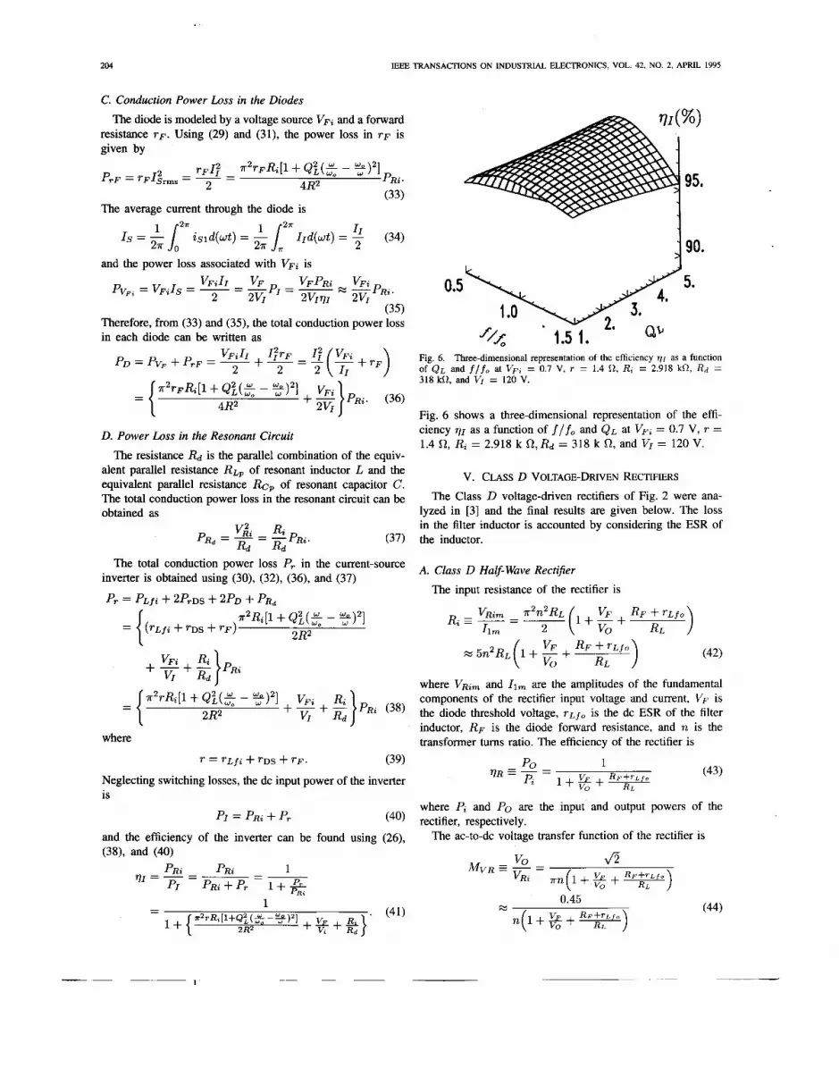
Fig. 6. Three-dimensional representation of the efficiency 71 as a function of QL and f/fo at Vpz = 0.7 V, T = 1.4 R, R, = 2.918 kfl, R d = 318 M , and VI = 120 V.
Fig. 6 shows a three-dimensional representation of the effi- ciency V I as a function of f/fo and QL at V F ~ = 0.7 V, T = 1.4 0, Ri = 2.918 k = 318 k 0, and VI = 120 V.
V. CLASS D VOLTAGE-DRIVEN RECTIFIERS
The Class D voltage-driven rectifiers of Fig. 2 were ana- lyzed in [3] and the final results are given below. The loss in the filter inductor is accounted by considering the ESR of the inductor.
A. Class D Half-Wave Rect$er The input resistance of the rectifier is
where V R ~ ~ and Ilm are the amplitudes of the fundamental components of the rectifier input voltage and current, VF is the diode threshold voltage, rLfo is the dc ESR of the filter inductor, RF is the diode forward resistance, and n is the transformer turns ratio. The efficiency of the rectifier is

KAZIMIERCZUK AND ABDULKARIM: CURRENT-SOURCE PARALLEL-RESONANT DClDC CONVERTER 205
where V& is the rms value of the rectifier input voltage. Com- VI. DESIGN PROCEDURE bining (20) and (44) produces the dc-to-dc voltage transfer function of the converter with a half-wave rectifier
V I R i J W VIMVR =
VO M = - = M VI nR(l+$+RT:fo)
(45) From (41) and (43), one obtains the converter efficiency
77 = V1VR = 1
The design procedure consists of the following steps: Step 1: Assume the overall converter efficiency V . Step 2: For full load, calculate the dc input power PI max,
the dc input current II the load resistance, RL min, and the dc load current Iomax. Step 3: Select a rectifier diode and identify its threshold voltage VF and its forward resistance RF. Step 4: Assume rLfo. Step 5: Calculate the rectifier efficiency VR. Step 6 Calculate MVR. Step 7 Calculate IDM, VDRM, ISM, and VSM. Step 8: Calculate the resonant components L and C. A transformer version of the converter with a center-tapped
rectifier will be designed to meet the following specifications: VI = 120 V, Vo = 48 V, Pomax = 25 W, and f < f o .
Assuming that the total efficiency of the converter is 71 = R. - V R ~ ~ - r2n2RL ( + 5 + RF + T L f o ) (47) 92%, the maximum dc input power can be calculated as
B. Class D Transformer Center-Tapped RectiJier
The parameters of the transformer center-tapped rectifier are
-
25 =27.17 W. (55) P o m a x - PIm,=- - - 8 VO RL
z - I1 m
0.92
The maximum value of the dc input current is (48)
PO 1 V R G - = pi l + $ + T RF+TLfo
(49)
Using (20) and (49), one arrives at the dc-to-dc voltage transfer function of the converter with a transformer center- tapped rectifier
2 ~ 1 R i d 1 + [QL(: - % ) I 2 V I M V R =
VO M z - = M VI nR(1+ $ + RFi:fO)
(50)
The efficiency of the converter is given by (46).
C. Class D Bridge RectiJier The parameters of the bridge rectifier are:
(51) . ,
(52)
(53)
From (20) and (53), one obtains the dc-to-dc voltage transfer function of the converter with a bridge rectifier
(54)
P I m a x - - 27 17 = 0.226 A. 120 (56) - 11 max = ISM max = - VI
The full-load resistance of the converter is
and the maximum value of the dc load current is
An MUR860 (Motorola) ultrafast pn-silicon diode has the threshold voltage VF = 0.7 V and the forward resistance RF = 0.1 Cl. Assuming n = 5 and rLfo = 1 R and using (47), one obtains the equivalent input resistance of the rectifier
- - r2 x 52 x 92 x (1 + + ") = 2918 R. (59) 8 92
Since the inverter output power is PRi = V&,J(2R), the amplitude of the inverter output voltage is
V R ~ ~ = d m = d 2 x 2918 x 25 = 382 V. (60)
From (48), the efficiency of rectifier V R is
1 R F + T L f o = 97.4%. (61) PO V R = - =
pi 1 + g + r Assuming the transformer tums ratio n = 5, the voltage transfer function of the rectifier can be found from (49)
__ I 1 ' I I

206
. ,
IEEE TRANSACTIONS ON INDUSTRIAL ELECTRONICS, VOL. 42, NO. 2, APRIL 1995
The rectifier diode peak current IDM and voltage VDRM are
IDM = Io = 0.52 A (63) (64) VDRM = ITVO = 3.14 x 48 = 150.8 V.
The required efficiency of the inverter is
71 = V / T R = 0.9210.974 = 0.96. (65)
The dc-to-dc voltage transfer function of the converter is
M = Vo/VI = QIMVIMVR = 481120 = 0.4 (66)
from which
Let us assume the resonant frequency f, = 100 kHz and the loaded quality factor QL = 3.5. Using (21), the switching frequency is f = 95 kHz. Hence, from (9),
1 cos$ = = 0.94 (68)
++ [ Q L ( ~ - % ) I 2
which gives $ = 19.76'. The component values of the resonant circuit are
= 1.29 mH (69) 2918 - R,
W,QL L = - -
2 x IT x loo x lo3 x 3.5 3.5
2 x IT x 100 x lo3 x 2918 = 1.96 nF. (70) c=- Q L - - w,R;
110
106
102
98
94
90 90 135 180 225 270 315 360 405 450
RL@) (a)
93
90
87
84
81
78
75
72 90 180 270 380 450
RLW)
(b)
402
397
392
387
382
377
372 90 135 180 225 270 315 360 405 450
RLW) (C)
The characteristic impedance is Z, = f l = 811 R. Equation (13) gives I, = 0.151 A. The maximum value of the switch peak voltage occurs at the lowest frequency fmin = 95 kHz. Hence, from (20), VSM = 401 V.
VII. EXPERIMENTAL RESULTS
The circuit designed in Section VI was implemented, using two IRF630 MOSFET's (International Rectifier), two ultrafast MUR1560 (Motorola) diodes in series with the MOSFET's, two ultrafast MUR860 (Motorola) rectifier diodes, input choke inductor Lf i = 10.5 mH, resonant inductor L = 1.33 mH, resonant capacitor C = 1.9 nF, transformer turns ratio n = 5, output filter inductor L f , = 14.7 mH, and filtering capacitance C f = 470 pF. The measured transformer primary inductance was L, = 14.73 mH and the transformer secondary inductance was L, = 682 pH. The MOSFET on-resistance was TDS = 0.4 R, the measured dc ESR of the input choke inductor was T L f i = 0.86 R, the measured dc ESR of the output filter inductor was rLfo = 1 R, the EPR of the resonant inductor measured at 100 kHz was RL, = 333 kR, and the EPR of the resonant capacitor measured at 100 kHz was Rc, = 7 MR.
Fig. 7. Measured and calculated characteristics of the current-source dddc converter as a function of load resistance RL at VI = 120 V and V, = 48 V. (a) Switching frequency f versus RI,. (b) Converter efficiency 17 versus RL. (c) Peak switch voltage VSM versus RL.
Hence, the total parallel parasitic resistance of the resonant circuit was Rd = 318 kR.
Performance characteristics of the converter were measured as functions of load resistance RL at VI = 120 V and Vo = 48 V. Fig. 7 shows measured and calculated plots of the switching frequency f , converter efficiency 7, and peak switch voltage VSM versus load resistance RL at VI = 120 V and V, = 48 V. As RL was increased from 90 to 450 R, the measured switching frequency increased from 100 to 106 kHz, the measured efficiency decreased from 86 to 73% as RL was increased from 90 to 450 R, and the measured peak switch voltage decreased from 400 to 376 V. The measured frequency range, required to control the output voltage, was wider than the calculated one. The measured efficiency was lower than the calculated one at all loads. The differences can be attributed to the fact that the same effects and parasitic components are not taken into account in the calculations, e.g., the influence of the skin and proximity effects on the inductor winding resistance.
I 1 ' I ~
I

KAZIMIERCZUK AND ABDULKARIM: CURRENT-SOURCE PARALLEL-RESONANT DCIDC CONVERTER 207
(C)
Fig. 8. Voltage and current waveforms of the switch Sa at V> = 120 V, L27 = 48 V, and different values of load resistances RL. (a) RL = 90 62. (b) R L = 180 6 2 . (c) R L = 450 6 1 . For (a) and (b), vertical: 200 V and 0.1 A/div, horizontal: 2 ps/div. For (c), vertical: 200 V and 0.04A/div, horizontal: 2 psldiv.
(C)
Fig. 9. Voltage and current waveforms of the rectifier diode at VI = 120 V, = 48 V, and different values of load resistances RL. (a) RL = 90 f2.
(b) RL = 180 6 1 . (c) RL = 450 n. Vertical: 50 V and 0.2 A/div, horizontal: 2 ps/div.
The voltage and current waveforms of the switch Sz and diode 0 2 at 15 = 120 and Vo = 48 V for RL = 90 R, 180 R, and 450 R are shown in Figs. 8 and 9, respectively. They are close to the theoretical waveforms shown in Fig. 3(a). The main difference is that the switch current waveform was rather trapezoidal than a square wave. This is because the input current had some ac ripple. The ripple-free input current and the square wave switch current required a large input inductance L f z which normally has a higher series equivalent resistance, increasing the conduction loss and the converter size. Therefore, a smaller input inductor was selected. The maximum value of the diode reverse voltage VDM occurred at full power. The switch voltage and current waveforms at VI = 120 and 140 V at fixed values of VO = 48 V and RL = 90 R are displayed in Fig. 10. As expected, a higher frequency was required to obtain the same output voltage at higher values of VI.
The inverter efficiency at full power can be estimated as follows: The power loss in the input choke is P L ~ ~ = rL& = 0.86 x 0.2262 = 44 mW. The power loss in the diode forward resistance r F is P T F = TFI;12/2 = 0.1 x 0.2262/2 = 3 mw. The power loss associated with VF is Pv, = VpIl/2 = 0.7 x 0.22612 = 79 mW. Thus, the total conduction loss in the diode is PO = P T ~ + PL, = 3 + 79 = 82 mW.
(b)
Fig. 10. Switch voltage and current waveforms at Vo = 48 V, RL = 90 62, and different voltages bk. (a) 1; I 120 V. (b) 1-r = 140 V. Vertical: 200 V and 0.2 A/div, horizontal: 2 ps/div.
The power loss in the resonant circuit is P R ~ = Vii/Rd = 2722/318000 = 0.232 W. Hence, the overall conduction loss

208 IEEE TRANSACTIONS ON INDUSTRIAL ELECTRONICS, VOL. 42, NO. 2, APRIL 1995
is PLS = P ~ f i + 2PvDS + 2PD + P R ~ = 44 + 2 x 26 + 2 x 82 + 232 = 492 mW. Thus, the efficiency of the inverter is 771 = 1 - &/Po = 1 - 0.492/25 = 98% and the converter efficiency is q = qIr)R = 0.98 x 0.974 = 95.45%.
8) The rectifier diodes turn off at a high dz/dt. Therefore, if pn junction diodes are used, the reverse-recovery spikes are generated, causing switching noise.
9) The converter has a nonpulsating input current.
VIII. CONCLUSION
A new circuit of the current-source parallel-resonant con- verter was introduced. A steady-state analysis, design equa- tions, the experimental results were given. The equations provide easy-to-use design tools and good insight into con- verter operation. Although the experiment was carried out at a relatively low power, the convertor is well suited for high-power applications.
The current-source parallel-resonant converter exhibits the following characteristics:
1) It can regulate the output voltage from full load to about 20% of full load, using a narrow frequency range. The measured frequency range was 100-106 kHz, i.e., 6%.
2) It can regulate the output voltage when the input voltage varies from 120 to 140 V. The measurement frequency range was 1W105 kHz, i.e., 5%.
3) It is an easy circuit to build and drive. Since both switches are referenced to ground, a pulse transformer or an optical coupler is not needed to drive the MOSFET’s.
4) The converter efficiency decreases with increasing load resistance RL because the ratio R/Rd increases with increasing RL .
5) Operation closer to the resonant frequency is desirable because the converter does not draw a high current at this frequency.
6) Above resonance, the series diodes of the inverter turn
REFERENCES
[I] J. G. Kassakian, “A new current mode sine wave inverter,” IEEE Trans Ind. Applicat., vol. 18, pp. 273-278, May/June 1982.
[2] H. Akagi, T. Sawae, and A. Nabae, “130 kHz 2.5 kW current source inverters using static induction transistors for induction heating ap- plications,’’ IEEE Trans. Power Electron., vol. 3, pp. 303-309, July 1988.
[3] M. K. Kazimierczuk, W. Szaraniec, and S . Wang, “Analysis and design of parallel resonant converter at high QL,” IEEE Trans. Aerospace and Electron. Syst., vol. 28, pp. 35-50, Jan. 1992.
Marian K. Kazimierczuk (M’91-SM’91) received the M.S., Ph.D., and D.Sci. degrees in electronics engineering from the Department of Electronics, Technical University of Warsaw, Poland, in 1971, 1978, and 1984, respechvefy.
He was a Teaching and Research Assistant from 1972 to 1978, and an Assistant Professor from 1978 to 1984 with the Department of Electronics, Institute of Radio Electronics, Technical University of Warsaw. In 1984, he was a Project Engineer for Design Automation, Inc., Lexington, MA. From
1984 to 1985, he was a Visiting Professor with the Department of Electrical Engineering, Virginia Polytechnic Institute and State University, Blacksburg. Since 1985, he has been with the Department of Electrical Engineering, Wright State University, Dayton, OH, where he is currently a Professor. His research interests are in resonant and PWM dc/dc power converters, dc/ac inverters, high-frequency rectifiers, electronic ballasta, magnetics, power semiconductor devices, and high-frequency, high-efficiency power tuned amplifiers. He has published over 130 technical papers, more than 60 of which have appeared in the IEEE Transactions and Journals.
Dr. Kazimierczuk received the 1991 IEEE Harrell V. Noble Award for his off at a very high &/d t , causing high reverse-recovery turn-off switching losses. ln the transistors turn on at nonzero voltage, resulting in turn-on switching losses.
7) Below resonance, the series diodes of the inverter turn off at zero d i /d t , yielding zero reverse-recovery losses. The MOSFET’s turn on at a low voltage, resulting in
contributions to the fields of aerospace, industrial, and power electronics. He is also a recipient of the 1991 Presidential Award for Faculty Excellence in Research and the 1993 Teaching Award from Wright State University. He Serves as an Associate mitor of the IEEE TRANSACTIONS ON CIRCUITS AND SYSTEMS and as an Associate Editor for the Joumal of Circuits, Systems, and
low switching losses. resonance is higher than that above resonance.
the efficiency Abdulkarim Abdulkarim, photograph and biography not available at time of publication.