copper and silver nanocrystals in lustre lead glazes: development and optical properties
TRANSCRIPT

Journal of the European Ceramic Society xxx (2006) xxx–xxx
Copper and silver nanocrystals in lustre lead glazes: Developmentand optical properties
J. Roquea,∗, J. Molerab, P. Sciauc, E. Pantosd, M. Vendrell-Saza
a Departament de Cristal·lografia Mineralogia i Diposits minerals, Universitat de Barcelona, 08028 Barcelona, Spainb Deptartament de Fısica, Universitat de Girona, 17071 Girona, Spain
c CEMES/CNRS, BP 94347 31055 Toulouse Cedex 4, Franced CCLRC Synchrotron Radiation Source/Daresbury Laboratory, Warrington WA4 4AD, UK
Received 21 September 2005; received in revised form 9 December 2005; accepted 16 December 2005
Abstract
In the early 9th century AD ancient potters of Iraq discovered that after firing some copper oxides and silver salts with clay, iron oxides and somesulphur compounds applied on a ceramic glaze produced a beautiful layer with a wide range of colours, from reddish to yellowish or even greenish,a ocrystals ofc cteristic glossb hape and thes ture linked toi been studiedb irradiationa the lustren as a functiono le distances.C e and copperm t. Diffusec he presenceo©
K
1
obmttAo
hiche the
ring,cora-thepos-
d of
ationss.thesis
thealkaliout
0d
12
nd some with a characteristic metallic copper or purplish shine. Modern studies of these layers showed that they are formed by nanopper and silver embedded in a glass matrix. Some attempts have been performed to understand ancient lustre coloration and charaut have failed to give a clear correlation between chemical composition and colour, and generally make some assumptions on the size of the nanoparticles and the lustre nanostructure. The aim of this paper is to establish a basis for understanding lustre nanostructs optical properties from a sequence of lustre reproductions on traditional lead glazed tiles. These modern lustre decorations havey means of optical microscopy, transmission electron microscopy and electron energy loss spectroscopy, UV–vis spectroscopy, lowngle X-ray diffraction, synchrotron radiation X-ray diffraction and electron microprobe analysis. These results show that changes inanostructure affect the glaze colour and shine during the lustre formation process. Lustre nanostructure showed crystal size rangef depth, that subsequently disappeared followed by an increase of nanoparticles mean diameter and reduction of the interparticonsequently, the dipole plasmon coupling between copper nanoparticles appeared, and seems to be responsible for the metallic shinetal like coloration of the copper lustre. However, colour from the glaze surface differs when calculated for diffuse or reflected ligh
oloration appears strongly affected by the copper nanocrystals, while specular coloration is not only affected by copper but also by tf an inhomogeneous distribution of silver nanocrystals which gives the lustre a characteristic purplish shine.2006 Elsevier Ltd. All rights reserved.
eywords: Firing; Nanocomposite; Optical properties; Glass ceramics
. Introduction
Lustre is one of the most interesting medieval ceramic dec-rations that corresponds to a nanostructured thin layer formedy metallic copper and silver nanocrystals embedded in a glassatrix.1–4 The earliest lustres were probably made in Iraq in
he early 9th AD and followed the expansion of the Arabian cul-ure through Spain and the rest of the western Mediterranean.5–7
ncient craftsmen, and still nowadays in some places of Spain,btained lustre by applying a copper and silver containing paint,
∗ Corresponding author. Tel.: +34 934021357; fax: +34 934021340.E-mail address: [email protected] (J. Roque).
mixed with water and/or vinegar, on a glazed ceramic, wafterwards, was annealed in a reducing atmosphere. Insidkiln, the raw paint reacted with the glaze surface, and after fithe remaining paint was washed off revealing the lustre detion beneath.7,8 Hence, traditional lustre technique is one ofoldest technologies known to achieve metal-glass nanocomites under relatively controlled conditions, without the neeultra high vacuum or clean environments.
Recently, it has been demonstrated that the lustre formprocess takes place as a result of an ionic exchange proce8–11
Nowadays, several methods have been reported for the synof nanosized particles of ceramic materials; among themion-exchange process has also been widely used to dopesilicate glasses. Ion-exchange in glass is typically carried
955-2219/$ – see front matter © 2006 Elsevier Ltd. All rights reserved.oi:10.1016/j.jeurceramsoc.2005.12.024
JECS-5914; No. of Pages
2 J. Roque et al. / Journal of the European Ceramic Society xxx (2006) xxx–xxx
by replacing monovalent alkali ions present in a surface layerof a glass substrate with different ions, usually from a moltensalt bath.12 Traditional lustre technology is based in the sameion-exchange process but instead of using a salt bath, the ion-exchange takes place between the copper and silver containingraw paint (traditionally called cosela) and the lead alkali glaze.10
Lustre required deep knowledge from the artisans of the rawmaterials used and on the kiln conditions, and their empiricalknowledge led to the achievement of colourful lustre decora-tions with a wide range of colours, from reddish to yellowishor even greenish, and some with a characteristic metallic orpurplish shine. But how were the optical glaze properties modi-fied by nanoparticles in order to fulfil these aesthetic purposes?Some attempts have been performed to understand ancient lustrecoloration but hardly give a clear correlation between chem-ical composition and lustre colour,13,14 and generally makesome assumptions regarding nanoparticles shape, size and lus-tre nanostructure. Hence, the aim of this paper is to establish abasis for understanding copper lustre nanostructure linked to itscolour and characteristic shine.
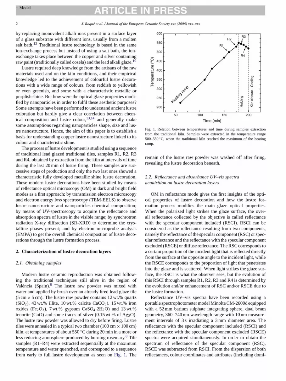
The process of lustre development is studied using a sequenceof traditional lead glazed traditional tiles, samples R1, R2, R3and R4, obtained by extraction from the kiln at intervals of timeduring the last 20 min of lustre firing. These samples are suc-cessive steps of production and only the two last ones showed acharacteristic fully developed metallic shine lustre decoration.T eanso eldm scopya servel ition;b anda tronr ys-t alysis( co-r
2
2
ow-i ofV ithw e tile( artz(otT stretk rls imumt uenf
Fig. 1. Relation between temperatures and time during samples extractionfrom the traditional kiln. Samples were extracted in the temperature range500–550◦C, when the traditional kiln reached the maximum of the heatingramp.
remain of the lustre raw powder was washed off after firing,revealing the lustre decoration beneath.
2.2. Reflectance and absorbance UV–vis spectraacquisition on lustre decoration layers
OM in reflectance mode gives the first insights of the opti-cal properties of lustre decoration and how the lustre for-mation process modifies the main glaze optical properties.When the polarized light strikes the glaze surface, the over-all reflectance collected by the objective is called reflectancewith the specular component included (RSCI). RSCI can beconsidered as the reflectance resulting from two components,namely the reflectance of the specular component (RSC) or spec-ular reflectance and the reflectance with the specular componentexcluded (RSCE) or diffuse reflectance. The RSC corresponds toa certain proportion of the incident light that is reflected directlyfrom the surface at the opposite angle to the incident light, whilethe RSCE corresponds to the proportion of light that penetratesinto the glaze and is scattered. When light strikes the glaze sur-face, the RSCI is what the observer sees, but the evolution ofthis RSCI through samples R1, R2, R3 and R4 is determined bythe evolution and/or enhancement of RSC and/or RSCE due tothe lustre formation.
Reflectance UV–vis spectra have been recorded using ap ppedw eamg sure-m Ther ) andt SCE)s thes SC),R bothr omi-
hese modern lustre decorations have been studied by mf reflectance optical microscopy (OM) in dark and bright fiodes as a first approach; by transmission electron micrond electron energy loss spectroscopy (TEM-EELS) to ob
ustre nanostructure and nanoparticles chemical composy means of UV-spectroscopy to acquire the reflectancebsorption spectra of lustre in the visible range; by synchroadiation X-ray diffraction (SR-XRD) to determine the cralline phases present; and by electron microprobe anEMPA) to get the overall chemical compostion of lustre deations through the lustre formation process.
. Characterization of lustre decoration layers
.1. Obtaining samples
Modern lustre ceramic reproduction was obtained follng the traditional techniques still alive in the regionalencia (Spain).8 The lustre raw powder was mixed water and applied by brush over an already fired lead glaz
5 cm× 5 cm). The lustre raw powder contains 12 wt.% quSiO2), 43 wt.% illite, 10 wt.% calcite CaCO3), 15 wt.% ironxides (Fe2O3), 7 wt.% gypsum CaSO4·2H2O) and 13 wt.%
enorite (CuO) and some traces of silver (0.15 wt.% of Ag2O).he lustre raw powder was allowed to dry before firing. Lu
iles were annealed in a typical two chamber (100 cm× 100 cm)iln, at temperatures of about 550◦C during 20 min in a more oess reducing atmosphere produced by burning rosemary.8 Tileamples (R1–R4) were extracted sequentially at the maxemperature and water quenched, and correspond to a seqrom early to full lustre development as seen onFig. 1. The
ce
ortable spectrophotometer model Minolta CM-2600d equiith a 52 mm barium sulphate integrating sphere, dual beometry, 360–740 nm wavelength range with 10 nm meaent intervals of 3 s irradiating a 3 mm diameter area.
eflectance with the specular component included (RSCIhe reflectance with the specular component excluded (Rpectra were acquired simultaneously. In order to obtainpectrum of reflectance of the specular component (RSCE was subtracted from RSCI. From the dispersion of
eflectances, colour coordinates and attributes (including d

J. Roque et al. / Journal of the European Ceramic Society xxx (2006) xxx–xxx 3
nant wavelengthλD, which corresponds to the hue) were calcu-lated according to the International Commission on Illumination(usually known as the CIE).
Additionally, absorption spectra in the UV–vis range havebeen also measured on thin sections of samples R1–R4 bymeans of spectrophotometer Shimadzu UV-2101 PC within therange 360–800 nm, with an interval of measurement of 0.5 nm,with a 0.5 mm beam footprint and at medium speed of mea-surement. The absorption band resulting from the dipole plas-mon resonance on metallic nanoparticles was expected to bemeasured.
2.3. Determining lustre chemical composition andnanostructure
Chemical analyses and distribution mappings of Cu and Ag,from the lustre layers were performed by microprobe analysis(EPMA Cameca SX-50) and the measurement conditions were20 kV and 15 nA probe current and 2 nA probe current for Nawith a measurement spot size of about 5�m. Analyses wereperformed directly on the surface of the samples. The penetra-tion depth was evaluated by Kanaya Okayama Range,15 givingabout 2.5�m in the glaze, and 1�m in a lustre layer, assumedto be formed by 50% glaze and 50% metal. The penetrationdepth is greater than the thickness of the lustre layer and themeasurements give an average value over the whole analyzedd
it-t haps os-s theg er top frome inneb ro-p mpl( is oft wera
singa atoa -t RDm -f imat ustret -rad syn-c hess h thgt ctiono anA Thea ei ataw
3. Optical properties and copper/silver nanoparticlesthin layer development in lustre decorations
3.1. Reflectance and absorbance in the UV–vis range
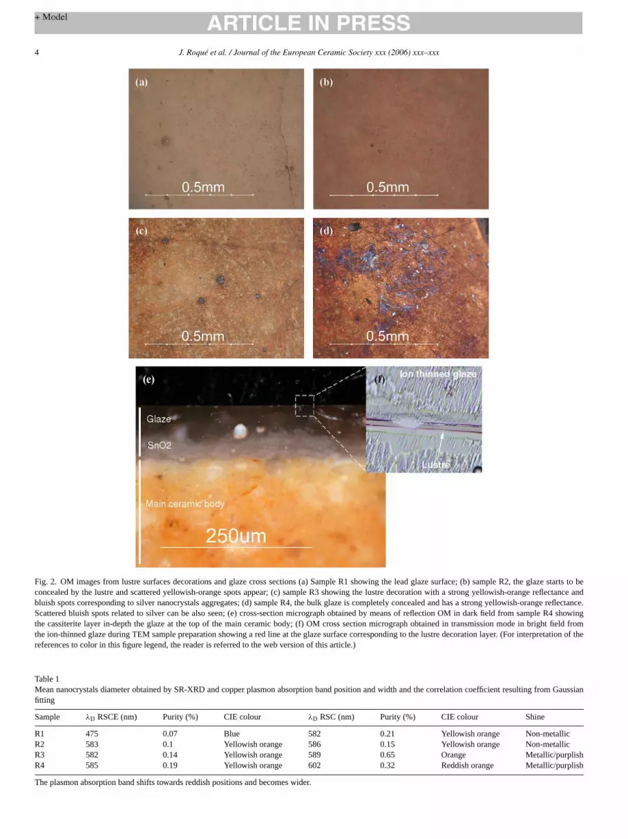
At first sight, from these modern lustre reproductions twosubsets of samples can be observed, according to colour andreflectance: Samples R1 and R2 do not present a metallic shinealthough they are coloured light orange while samples R3 andR4 exhibit a metallic and purplish shine and have a metalliccopper-like colouration.
In Fig. 2, OM in reflectance mode images are shown. Imagesfrom samples R1 and R2 show small yellowish-orange brightspots with sizes up to 5�m, with a higher density in sample R2than in R1. Samples R3 and R4 both show a fully developed lus-tre with a nice gold metallic shine. R3 shows a higher reflectanceat the edges than at the centre of the lustre decorations. Theedges appear bright orange and contain some highly reflectingyellowish-orange spots; the centre shows a lower reflectance andorange-yellow colour. R4 exhibits a highly reflecting gold-likeedge and also an orange-yellow colour. It is interesting to noticethe presence of scattered blue spots on samples R3 and R4 thatcorrespond to accumulations of metallic silver particles.4
The RSCE and RSC spectra acquired in the 360–800 nmwavelength range from the lustre decoration surfaces show aclear evolution from sample R1 to sample R4 as seen inFig. 3.T glazewp d thea an ins round5 Dur-i n oft d R4,l rationl
mpleR ,t 2 witha witha trongr n theb ectraf d onea ptionb
omt ted inT tionf R1t thec40 firmt luesf tionp
epth.TEM Philips CM20 coupled with DIGIPEELS 666 perm
ed the characterization the nanostructure, nanoparticle sizes and chemical composition. With TEM-EELS, it is pible to establish the evolution of the nanoparticles insidelass matrix through samples R1, R2, R3 and R4. In orderform TEM-EELS observations, glaze cross-sectionsach sample were prepared, polished mechanically and thy means of Ar+ ion bombardment to achieve the appriate thickness to allow electrons pass through the saaround 100 nm). To perform chemical elemental analyshe nanoparticles electron energy loss spectrums (EELS)cquired.
Crystalline phases were identified and studied by XRD uSiemens D-500 equipped with a secondary monochrom
nd Cu tube (wavelength 1.5418A). According to the nanosructured thin layer nature of lustre, low irradiation angle Xeasurements (2.0 s counting time and 0.05 2θ step) were per
ormed to determine the crystalline phases present. To esthe mean size of the copper metal nanoparticles on the lhin slides of the glazes were prepared and examined by Xiffraction in transmission geometry at station 9.6 of thehrotron radiation source (SRS) at Daresbury Laboratory. Tections were thin enough to allow the X-rays to pass througlass and diffract. The wavelength at station 9.6 was 0.87A and
he collimator defining the beam footprint had a cross-sef 200�m. The data collection time was typically 60 s usingDSC Quantum-4 CCD detector at a distance of 160 mm.ctive area of the detector is 2304× 2304 pixels. The pixel siz
s 81.6�m× 81.6�m and the dynamical range 16-bit. The dere processed using the ESRF package FIT2D.16
e,
d
e
e
r
te,
y
ee
he RSCE spectra for sample R1 correspond to a leadith a strong absorption in the blue region,17 while for sam-les R2, R3 and R4, the overall absorption increase anbsorption in the blue region is much less pronounced thample R1. Moreover, a small absorption band appears a60 nm and increases from sample R2 to sample R4.
ng the lustre formation, the reflectance on the red regiohe RSCE spectra increases through samples R2, R3 aninked to the presence and development of the lustre decoayer.
The RSC spectra show an increase of intensity from sa1 to R4 as seen inFig. 3. According to the intensity of RSC
wo sets of samples can be established: Samples R1 and Rvery low or non-existent RSC, and samples R3 and R4higher RSC. In samples R3 and R4, the RSC show a s
eflectance in the red region, and surprisingly also reflects ilue region. Two absorption bands appear in the RSC sp
rom samples R3 and R4, one around 560 nm and a seconround 430 nm, with a strong increase in the 560 nm absorand from sample R3 to R4.
Dominant wavelengthλD values have been calculated frhe RSC and RSCE spectra for each sample and are lisable 1. The calculated colour from the RSC show an evolurom λD 582 nm and 0.21% excitation purity on sampleo λD 602 nm 0.32% excitation purity in sample R4, andalculated colour from the RSCE showed an evolution fromλD75 nm and 0.07% excitation purity on sample R1 toλD 585 nm.19% excitation purity on sample R4. These results con
hat colouration of lustre evolves towards more reddish varom the very beginning until the end of the lustre formarocess.
4 J. Roque et al. / Journal of the European Ceramic Society xxx (2006) xxx–xxx
Fig. 2. OM images from lustre surfaces decorations and glaze cross sections (a) Sample R1 showing the lead glaze surface; (b) sample R2, the glaze starts to beconcealed by the lustre and scattered yellowish-orange spots appear; (c) sample R3 showing the lustre decoration with a strong yellowish-orange reflectance andbluish spots corresponding to silver nanocrystals aggregates; (d) sample R4, the bulk glaze is completely concealed and has a strong yellowish-orange reflectance.Scattered bluish spots related to silver can be also seen; (e) cross-section micrograph obtained by means of reflection OM in dark field from sample R4 showingthe cassiterite layer in-depth the glaze at the top of the main ceramic body; (f) OM cross section micrograph obtained in transmission mode in bright field fromthe ion-thinned glaze during TEM sample preparation showing a red line at the glaze surface corresponding to the lustre decoration layer. (For interpretation of thereferences to color in this figure legend, the reader is referred to the web version of this article.)
Table 1Mean nanocrystals diameter obtained by SR-XRD and copper plasmon absorption band position and width and the correlation coefficient resulting from Gaussianfitting
Sample λD RSCE (nm) Purity (%) CIE colour λD RSC (nm) Purity (%) CIE colour Shine
R1 475 0.07 Blue 582 0.21 Yellowish orange Non-metallicR2 583 0.1 Yellowish orange 586 0.15 Yellowish orange Non-metallicR3 582 0.14 Yellowish orange 589 0.65 Orange Metallic/purplishR4 585 0.19 Yellowish orange 602 0.32 Reddish orange Metallic/purplish
The plasmon absorption band shifts towards reddish positions and becomes wider.

J. Roque et al. / Journal of the European Ceramic Society xxx (2006) xxx–xxx 5
Fig. 3. RSCE and RSC spectra on lustre reproductions: (a) sample R1 with a RSCE corresponding to a lead glaze with a strong absorption at the beginning oftheblue region and almost no RSC; (b) sample R2, the lustre layer conceals the glaze increasing its RSCE in the red region and very low RSC appears; (c) sample R3increase its RSCE in the red region and RSC is strongly enhanced; (d) sample R4, the RSCE also increase its reflectance on the red region and RSC is stronglyenhanced.
From the absorption spectra acquired in the 360–800 nmwavelength range from thin sections using transmission geom-etry and shown inFig. 4, two main absorption bands appear inFig. 4(a): one in the blue region, constant in all the samples andrelated to the absorption of the lead glaze substrate, and a secondone at 560 nm corresponding to the dipolar plasmon absorp-tion of metallic copper nanoparticles,18 which only occurs onsamples R2, R3 and R4. The absorption band at 560 nm hasbeen Gaussian fitted and the results are listed inTable 2. Theyshow a red shift from 567 nm in sample R2 to 577 nm insample R3 and 585 nm in sample R4. Normalized spectra inFig. 4(b) from samples R2, R3 and R4 confirm this red shift and
Table 2Dominant wavelength (λD) from RSCE and RSC spectra acquired on samplesR1, R2, R3 and R4
Sample Mean Cu nanorystalsdiameter (nm)
SPR (nm) FHW (nm) CorrelationcoefficientR2
R1 – – – –R2 9.29± 1.91 567 41.61 0.99953R3 9.14± 0.88 577 48.66 0.99978R4 21.95± 0.77 585 49.02 0.99977
show an increase of the absorption in the red region resultingfrom an increase on the right shoulder of the absorption band.This absorption becomes more important from sample R3 tosample R4.
3.2. Chemical composition and copper/silver distribution
EPMA chemical profiles were acquired directly on the sur-face of the samples crossing white glaze and lustre decorationand the mean composition has been calculated and listed inTable 3. Chemical differences are seen on the lustre from theearly formation stage of lustre, sample R1, to the full lus-tre formation on sample R4. An increase of copper and silverconcentration, from 0.22± 0.13 to 5.32± 0.75 wt.% and from0.03± 0.04 to 0.98± 0.30 wt.%, respectively, and a decreaseon sodium and potassium concentration, from 0.70± 0.06 to0.50± 0.04 wt.% and from 3.43± 0.28 to 1.99± 0.12 wt.%,respectively, is observed during the lustre formation process.Copper increases rapidly at the beginning of the lustre formationprocess (from 0.2± 0.1 wt.% on sample R1 to 4.0± 0.6 wt.%on sample R2) while later silver increases suddenly (from0.05± 0.05 wt.% on sample R2 to 1.0± 0.4 wt.% on sample

6 J. Roque et al. / Journal of the European Ceramic Society xxx (2006) xxx–xxx
Tabl
e3
Ele
men
talc
ompo
sitio
nof
glaz
esob
tain
edfr
omE
MP
Ada
tata
ken
onth
elu
stre
glaz
essu
rfac
esin
wt.%
for
sam
ples
R1,
R2,
R3
and
R4
Sam
ple
Na
KM
gA
lS
iC
aF
eC
uA
gP
bO
Tota
l
R1
0.70
±0.
063.
43±
0.28
0.04
±0.
032.
67±
0.10
21.7
7±0.
150.
75±
0.19
0.06
±0.
050.
22±
0.13
0.03
±0.
0436
.35±
0.78
31.3
4±0.
1797
.37±
1.98
R2
0.69
±0.
063.
32±
0.36
0.06
±0.
022.
88±
0.07
21.9
7±0.
250.
85±
0.09
0.08
±0.
081.
31±
0.54
0.05
±0.
0534
.62±
0.58
32.8
4±0.
2496
.67±
2.34
R3
0.56
±0.
051.
98±
0.10
0.03
±0.
022.
52±
0.07
21.0
3±0.
170.
66±
0.07
0.07
±0.
043.
98±
0.58
1.02
±0.
3835
.10±
0.74
30.9
0±0.
1897
.84±
2.4
R4
0.50
±0.
041.
99±
0.12
0.04
±0.
012.
15±
0.05
20.6
9±0.
170.
73±
0.05
0.07
±0.
045.
32±
0.75
0.98
±0.
3034
.40±
0.66
31.0
3±0.
1897
.90±
2.37
An
incr
ease
inco
pper
and
silv
eran
da
decr
ease
inso
dium
and
pota
ssiu
mar
ese
enth
roug
hth
elu
stre
form
atio
npr
oces
s.
Fig. 4. Absorption spectra obtained from lustre reproductions R1, R2, R3 andR4. (a) Strong absorption at the beginning of the blue region due to the lead glazeand copper dipole plasmon absortion band. (b) Copper dipole plasmon absorp-tion band shift in position and width as a consequence of dipole interactionsbetween nanoparticles through samples R1, R2 and R3.
R3). This has been interpreted as a result of the chemicalmechanisms responsible for lustre formation: ion-exchange ofalkalies (Na and K) by Cu and Ag, diffusion of the metalions into the glaze and reduction of the metal ions to metallicnanoparticles.8
Chemical mappings obtained directly on lustre decorationshow a homogenous distribution of copper but an inhomo-geneous distribution of silver. InFig. 5, copper appears welldistributed over all the lustre decoration but silver appears toform spots some several tens of microns in width, exclud-ing in some cases the presence of copper. These silverspots are linked to blue spots seen on OM in reflectancemode. Also, an inverse correlation between the presenceof copper and silver and alkalies such as sodium is seen.The copper and silver-rich areas corresponding to the lus-tre decoration lines are much less rich in sodium than theglaze.

J. Roque et al. / Journal of the European Ceramic Society xxx (2006) xxx–xxx 7
Fig. 5. Chemical maps obtained by means of EMPA on a 1 mm× 1 mm areaon the surface of sample R4. (a) Accordingly to OM images an inhomogeneoudistribution of silver forming scattered silver-rich spots on the lustre decora-tion surface can be seen. (b) Homogenous distribution of copper on the lustrdecoration surface. From these maps, the silver-rich spots seem to exclude tpresence of copper.
3.3. Copper nanoparticles development inside the glassmatrix
The TEM images inFig. 6 show that nanoparticles varyin size and amount during the lustre formation process fromsample R1 to R4. In sample R1, small nanoparticles of abou10 nm mean diameter scattered throughout in the glass matrican be observed. Surprisingly, nanoparticles appear deep insidinto the glaze, 200 nm below the glaze surface. In sample R2nanoparticles appear to form a discontinuous layer parallel tothe glaze surface and two populations of nanoparticles can b
distinguished according to their size: nanoparticles with a meandiameter about 10 nm and nanoparticles with a mean diameteraround 20 nm. The bigger nanoparticles appeared in the first100 nm depth into the glaze, and the smaller occur from 100 nmup to 200 nm in depth. In sample R3, a higher density of nanopar-ticles appears when compared to the previous samples, forminga continuous layer parallel to the glaze surface and in a rangeof mean diameters from 10 to 20 nm. The bigger nanoparticlesappear in the first 100 nm depth into the glaze while the smallerones appeared from 100 nm up to 200 nm depths. In sample R4,only one population of nanoparticles with a mean diameter of20 nm appeared parallel to the glaze surface, forming a continu-ous layer at 100 nm depth into the glaze. EELS spectra acquiredon three nanoparticles on sample R4 confirmed that they aremainly copper as shown inFig. 7.
It is worth noticing that while observing the samples throughTEM, the glass matrix suffered alteration due to the interactionof the electron beam with the sample, resulting in a granulartexture which should not be confused with the nanoparticlesforming the lustre metal-glass nanocomposite.
Low irradiation angle diffraction patterns were acquired inorder to determine the main crystalline phases present. The onlycrystalline phases determined are metallic copper and silver asseen inFig. 8and listed onTable 4. The lustre formation processgives no crystalline phase initially in sample R1, metallic copperappears on sample R2, R3 and R4, and small amounts of metallics
om-ec seenI no lesR ur 2 tos t ands (seeF r ofc sianfi fromt ua-t ound9 withv rystald zed inT ze oft ree-m 1 1 1r
4
indi-c strel theg ep ic sil-v en in
s
ehe
txe,
e
ilver in sample R3 and R4.SR-XRD diffraction patterns obtained in transmission ge
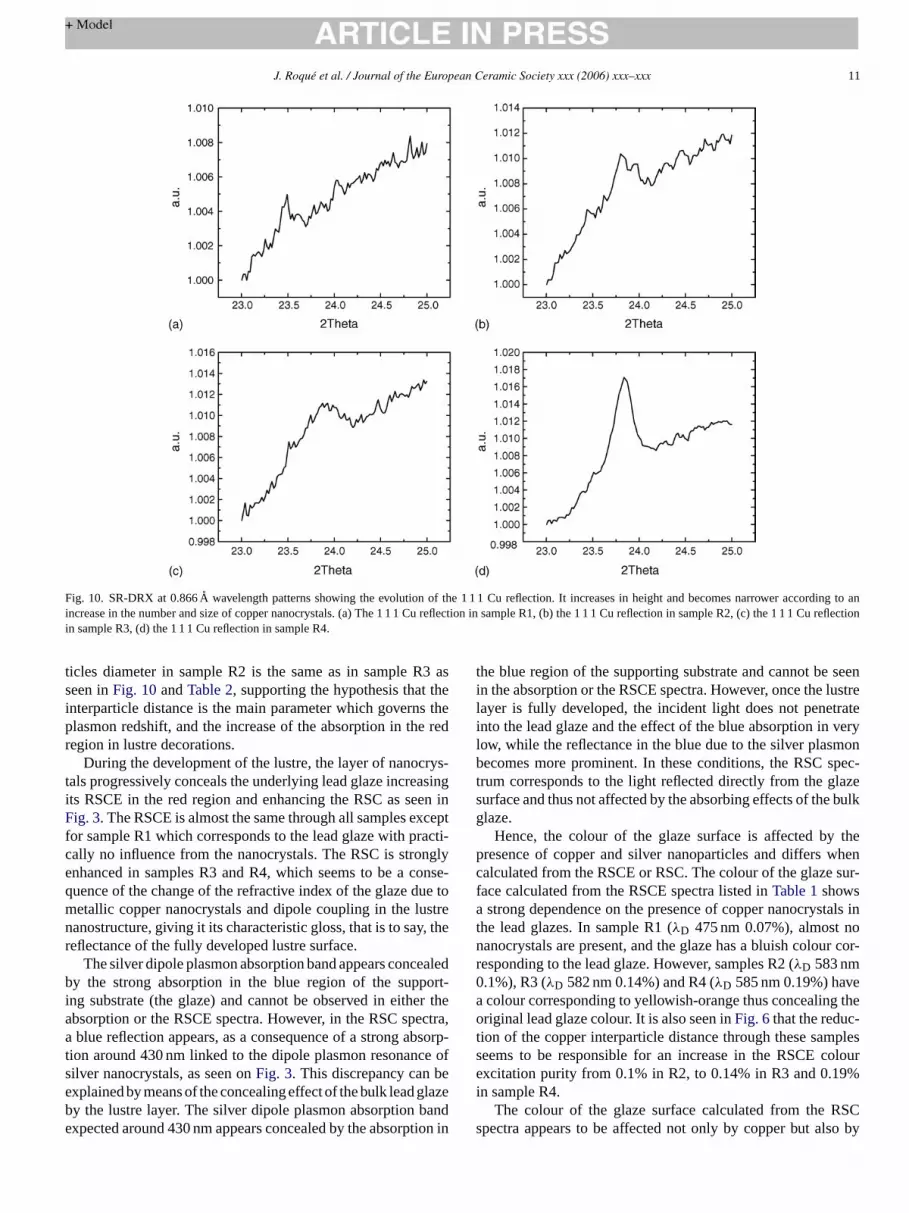
try revealed not only copper but also cassiterite (SnO2) allo-ated in-depth the glaze near to the main ceramic body asn Fig. 9and listed inTable 5. Metallic copper showed evolutiof the 1 1 1 diffraction line of metallic copper through samp2, R3 and R4 as seen InFig. 10. The intensity of the 1 1 1 C
eflection increases and narrows in width from sample Rample R4, in agreement with the increase in the amounize of copper nanocrystals observed in the TEM imagesig. 1 andTable 2). In order to estimate the mean diameteopper nanocrystals, the diffraction line profile was Gaustted and the mean sizes of the copper particles calculatedhe full width at half maximum applying the Scherrer eqion. The mean nanocrystal diameter for sample R2 is ar.28 nm, for sample R3 the mean is close to sample R2alues around 9.14 nm, but for sample R4 the mean nanociameter increases to 21.95 nm. The results are summariable 2. These data confirm an increase in the average sihe copper nanoparticles only from sample R3 to R4, in agent with the sizes observed at TEM. No metallic copper
eflection appears in sample R1.
. Discussion and interpretation of the measurements
Chemical analyses during the lustre formation processate that the incorporation of copper and silver in the luayer is linked to a decrease in the alkalies (Na and K) fromlaze as seen onTable 1. Metallic copper is the main crystallinhase present in the lustre reproductions; however, metaller has been detected by means of low angle XRD as se

8 J. Roque et al. / Journal of the European Ceramic Society xxx (2006) xxx–xxx
Fig. 6. TEM images obtained during the copper nanocrystallization process inside the glass matrix. (a) Sample R1 small nanoparticles about 10 nm meandiameterappear scattered in the glass matrix. (b) Sample R2, two populations of copper nanoparticles of 10 and 20 nm mean diameter appear forming a discontinuous layerparallel to the glaze surface. (c) Sample R3, two populations of copper nanoparticles of 10 and 20 nm mean diameter appear forming a continuous layer parallel tothe glaze surface. (d) Sample R4, a continuous almost monolayer of copper nanoparticles with a mean diameter of 20 nm appears parallel to the glaze surface.
Figs. 8 and 10. Metallic silver nanocrystals are heterogeneouslydistributed in clusters in the lustre decoration, and as SR-XRD intransmission geometry provides low statistics on the surface, itis difficult to get any signal from the silver nanocrystals presentin the glaze.
Metallic copper nanocrystals increase in amount throughsamples R1, R2, R3 and R4 according to the 1 1 1 reflectionintensity, but only in size for sample R4 as seen inFig. 3 andTable 2. For samples R1, R2 and R3, the lustre nanostructureexhibits nanocrystal size dependence on the depth, suggestingthat a Cu+ gradient exists inside the bulk glaze as seen inFig. 6.This gradient can be explained as a result of the ion-exchangeprocess. Close to the glass surface, the ionic-exchange processhas been more intense, there is a higher Cu+ concentration, andcopper nanocrystals can grow easily up to 20 nm, but deeperinto the glaze, where the ion-exchange process is less intense
the concentration of Cu+ is less, copper nanocrystals do notgrow so easily and only nanocrystals around 10 nm in diameterare present. However, in sample R4, only nanocrystals with amean diameter of 20 nm appear close to the glass surface. Thedisappearance of smaller nanocrystals in sample R4 could bedue to a ripening process as in a closed system where the massof the crystals is conserved (Oswald ripening). It would implythat in sample R4, the ion-exchange process has been exhaustedat the outermost part of the glaze and then, some of the smallercrystalline phases dissolve to supply material to other crystalsof the same phase that are growing. Thus, in sample R4, smallmetallic copper nanocrystals, less stable than bigger nanocrys-tals, have been redissolved to coarser the bigger nanocrystalswhich are close to the glass surface.
Reflecting OM as seen inFig. 2, indicates that the lustreappears scattered at first, forming small spots linked to copper

J. Roque et al. / Journal of the European Ceramic Society xxx (2006) xxx–xxx 9
Table 4Spacing list from the crystalline phases present in the glazes and obtained from DRX data in reflection geometry and transmission geometry
DRX technique Sample d (A) (measured) d (A) (JCPDF) h k l Phase
Low irradiation angle at 1.5418A in reflection geometry R1 – – – –
R2 2.08 2.08 1 1 1 CuM
R3 2.37 2.36 1 1 1 AgM2.08 2.08 1 1 1 CuM1.80 1.81 2 0 0 CuM1.27 1.28 2 2 0 CuM
R4 2.37 2.36 1 1 1 AgM2.08 2.08 1 1 1 CuM1.80 1.81 2 0 0 CuM1.27 1.28 2 2 0 CuM
SRS Station 9.6 at 0.866A in transmission geometry R1 3.32 3.35 1 1 0 SnO2
2.65 2.64 1 0 1 SnO22.38 2.37 2 0 0 SnO21.74 1.76 2 1 1 SnO2
R2 3.32 3.35 1 1 0 SnO22.65 2.64 1 0 1 SnO22.38 2.37 2 0 0 SnO22.09 2.08 1 1 1 CuM1.74 1.76 2 1 1 SnO2
R3 3.32 3.35 1 1 0 SnO22.65 2.64 1 0 1 SnO22.38 2.37 2 0 0 SnO22.09 2.08 1 1 1 CuM1.74 1.76 2 1 1 SnO2
R4 3.32 3.35 1 1 0 SnO22.65 2.64 1 0 1 SnO22.38 2.37 2 0 0 SnO22.09 2.08 1 1 1 CuM1.74 1.76 2 1 1 SnO2
Fig. 7. Characteristic metallic copper EELS spectra obtained on three differentnanocrystals from sample R4. The three spectra show the absorption edges (A)Cu L3 at 931 eV and (B) Cu L2 at 951 eV characteristics of copper.
nanoparticles agglomerates which increase in density and jointogether until they occupy the whole surface. These areas areorange or yellow depending of the spot size, and the metallicshine is first achieved at the edges of the lustre decorations andis linked to the presence of more yellow spots. Some blue andpurple spots appear in samples R3 and R4 corresponding to clus-ters of metal silver particles according toFigs. 2 and 5. Thefinal, almost homogeneous orange-yellow surface containingsome blue spots of silver fits with OM observations of medievallustres.1,4
Reflectance and absorbance spectra (Figs. 3 and 4) obtainedfrom these samples confirm that lustre optical properties such as
Table 5Crystalline phases list obtained from DRX data in reflection geometry and intransimission geometry from lustre glazes
DRX technique Phase JCPDF file
Low irradiation angle at 1.5418Ain reflection geometry
AgM 2-1098
CuM 89-2838
SRS Station 9.6 at 0.866A intransmission geometry
SnO2 41-1445
CuM 89-2838

10 J. Roque et al. / Journal of the European Ceramic Society xxx (2006) xxx–xxx
Fig. 8. Low angle XRD pattern acquired on lustre reproductions surfaces. (a) Sample R1, no crystalline phases are present; (b) sample R2, only metallic copperappears; (c) sample R3 and (d) sample R4, metallic copper and silver are detected.
absorption, reflectance and thus colour, strongly depend on thedipole plasmon resonance of the metallic copper and silver par-ticles present in the lustre layer. The dipole plasmon resonanceoccurs when metallic nanoparticles are irradiated by light, thenthe oscillating electric field causes the conduction electrons tooscillate coherently displacing the electron cloud from to thenuclei. The absorption produced by the collective oscillation ofthe electrons is known as the dipole plasmon resonance of theparticle, which for spherical copper nanoparticles is expected tobe at 560 nm and for silver nanoparticles is at 430 nm.19,20
However, there are complicating factors in understandingoptical properties of the nanoparticles appearing in lustre deco-rations, e.g. as particles maybe are close enough together to give
electromagnetic coupling, and/or the supporting substrate maychange the spectra expected.21–23
The copper nanoparticles in lustre decoration increase innumber from sample R2 to sample R4, reducing the inter-crystalline distances, thus resulting in changes in the plasmonpeak position and width as a consequence of dipole interactionsamong the nanoparticles. In sample R2, there is a large inter-particle distance, the particles “perceive” little change in theenvironment and there is no dipole coupling, while in samplesR3 and R4, the interparticle distances are smaller and the dipoleplasmon resonance absorption band changes showing a red shiftand an absorption increase in the red region seen inFig. 4as inThearith et al.23 It is interesting to note that the mean nanopar-
F ample cassiterite( . CuM . Cassh t in-d opac
ig. 9. SR-DRX at 0.866A wavelength azimuth transform pattern from sSnO2) and metallic copper (CuM) as the main crystalline phases presentas been detected only in transmission geometry because is only presen
R4, with clear bump at low angle associated to amorphous glass and1 1 1 reflection is wide giving and indirect evidence of its nanometric sizeiteriteepth the glaze, near to the main ceramic body in low amounts, acting asifier.
J. Roque et al. / Journal of the European Ceramic Society xxx (2006) xxx–xxx 11
Fig. 10. SR-DRX at 0.866A wavelength patterns showing the evolution of the 1 1 1 Cu reflection. It increases in height and becomes narrower according to anincrease in the number and size of copper nanocrystals. (a) The 1 1 1 Cu reflection in sample R1, (b) the 1 1 1 Cu reflection in sample R2, (c) the 1 1 1 Cu reflectionin sample R3, (d) the 1 1 1 Cu reflection in sample R4.
ticles diameter in sample R2 is the same as in sample R3 asseen inFig. 10andTable 2, supporting the hypothesis that theinterparticle distance is the main parameter which governs theplasmon redshift, and the increase of the absorption in the redregion in lustre decorations.
During the development of the lustre, the layer of nanocrys-tals progressively conceals the underlying lead glaze increasingits RSCE in the red region and enhancing the RSC as seen inFig. 3. The RSCE is almost the same through all samples exceptfor sample R1 which corresponds to the lead glaze with practi-cally no influence from the nanocrystals. The RSC is stronglyenhanced in samples R3 and R4, which seems to be a conse-quence of the change of the refractive index of the glaze due tometallic copper nanocrystals and dipole coupling in the lustrenanostructure, giving it its characteristic gloss, that is to say, thereflectance of the fully developed lustre surface.
The silver dipole plasmon absorption band appears concealedby the strong absorption in the blue region of the support-ing substrate (the glaze) and cannot be observed in either theabsorption or the RSCE spectra. However, in the RSC spectra,a blue reflection appears, as a consequence of a strong absorp-tion around 430 nm linked to the dipole plasmon resonance ofsilver nanocrystals, as seen onFig. 3. This discrepancy can beexplained by means of the concealing effect of the bulk lead glazeby the lustre layer. The silver dipole plasmon absorption bandexpected around 430 nm appears concealed by the absorption in
the blue region of the supporting substrate and cannot be seenin the absorption or the RSCE spectra. However, once the lustrelayer is fully developed, the incident light does not penetrateinto the lead glaze and the effect of the blue absorption in verylow, while the reflectance in the blue due to the silver plasmonbecomes more prominent. In these conditions, the RSC spec-trum corresponds to the light reflected directly from the glazesurface and thus not affected by the absorbing effects of the bulkglaze.
Hence, the colour of the glaze surface is affected by thepresence of copper and silver nanoparticles and differs whencalculated from the RSCE or RSC. The colour of the glaze sur-face calculated from the RSCE spectra listed inTable 1showsa strong dependence on the presence of copper nanocrystals inthe lead glazes. In sample R1 (λD 475 nm 0.07%), almost nonanocrystals are present, and the glaze has a bluish colour cor-responding to the lead glaze. However, samples R2 (λD 583 nm0.1%), R3 (λD 582 nm 0.14%) and R4 (λD 585 nm 0.19%) havea colour corresponding to yellowish-orange thus concealing theoriginal lead glaze colour. It is also seen inFig. 6that the reduc-tion of the copper interparticle distance through these samplesseems to be responsible for an increase in the RSCE colourexcitation purity from 0.1% in R2, to 0.14% in R3 and 0.19%in sample R4.
The colour of the glaze surface calculated from the RSCspectra appears to be affected not only by copper but also by

12 J. Roque et al. / Journal of the European Ceramic Society xxx (2006) xxx–xxx
silver nanocrystals. According toFig. 6 andTable 1when thecopper interparticle distances are reduced calculatedλD fromRSC is shifted towards reddish values; in samples R1 (λD 5820.21%) and R2 (λD 586 nm 0.15%) with a colour correspond-ing to yellowish-orange, sample R3 (λD 589 nm 0.65%) with acolour corresponding to orange, while in sample R4 (λD 602 nm0.32%), the colour corresponds to reddish-orange. However, thespecular reflectance in some parts of lustre decorations appearspurple. Observation of the specular reflectance through a reflect-ing microscope confirms the presence of blue spots that EPMAmappings demonstrated that correspond to silver clusters as seenin Figs. 2 and 5. Thus, the blue and red reflectance componentseen inFig. 3 corresponds to silver and copper nanoparticles,respectively, and the resulting mixture of blue plus red is inter-pretated by the eye as purple.
It is worth noticing that TEM-EELS measurements alter theglass matrix resulting to a granular texture which is not directlyrelated to the copper nanocrystallization process in lustre forma-tion as seen inFig. 6. This alteration may have occurred becauseof the interaction of the TEM electron beam with the samplewhich produces a reducing effect on the major constituent chem-ical species present in the glass matrix.
5. Conclusions
Lustre nanostructure shows crystal size dependence as a func-tf withN ofm
Cun comp esui caui ipolep ands
henc col-o hica onlya ogen ilvern , bui le fot olouw
RDr EM-E SRX
A
by thp nce
and by a project of the Comunidad de Trabajo de los Piri-neos (CTP/DAER 03007514), through which the collaborationbetween researchers of the CEMES Toulouse and the Univer-sity of Barcelona has been possible. The authors would also liketo thank Mr. Alejandro Barbera, a potter still working in lus-tre, for his help and facilities in traditional firing. Also, thanksare due to Dr. Josefina Perez-Arantegui of the Universidad deZaragoza, Dr. Isabel Pastoriza of the Universidad de Vigo andDr. Triniat Pradell of the Universitat Politecnica de Catalunyafor fruitful discussions. We are grateful to Anne-Sophie Rammfrom CEMES Toulouse for her help and guidance in the TEMsample preparations. The SR data were collected at DaresburyLaboratory during a visit in the framework of the Memorandumof Understanding signed between CCLRC and UB/UPC.
References
1. Perez-Arantegui, J., Molera, J., Larrea, A., Pradell, T., Vendrell-Saz, M.,Borgia, I., Brunetti, B. G., Cariati, F., Fermo, P., Mellini, M., Sgamellotti,A. and Viti, C., J. Am. Ceram. Soc., 2001,84, 442–446.
2. Perez-Arantegui, J. and Larrea, A.,Trends Anal. Chem., 2003, 22(5),327–329.
3. Padeletti, G. and Fermo, P.,Appl. Phys., 2003,A76, 515–525.4. Roque, J., Pradell, T., Molera, J. and Vendrell-Saz, M.,J. Non-Cryst.
Solids, 2005,351, 568–572.5. Perez-Arantegui, J., Larrea, A., Molera, J., Pradell, T. and Vendrell-Saz,
M., Appl. Phys., 2004,A79, 235–239.6. Caigher-Smith, A.,Lustre Pottery: Technique, Tradition and Innovation
s,
ll-
s,
1 E.
1 and
1 ,
1
1 A.,
11 user-
1
1 .,
1
2
22
2
ion of depth, supporting the proposition that Cu+ and Ag+ ionsrom the raw paint applied on the surface are exchangeda+ and K+ from the glaze, followed by the crystallizationetallic copper nanocrystals inside the glass matrix.During the lustre formation, the centre of mass of the
anoparticles has a tendency to shift toward the surface acanied by the disappearance of the smaller nanocrystals, r
ng from a pronounced coarsening of the nanoparticles andng a reduction of the interparticle distances. Thus, the dlasmon coupling between copper nanoparticles appearseems to be responsible for the lustre shine and colour.
Nevertheless, the colour from the glaze surface differs walculated from diffuse or specularly reflected light. Diffuseration appears strongly affected by copper nanocrystals, wre the most abundant, while specular coloration is notffected by copper but also by the presence of an inhomeous distribution of silver nanocrystals. The effect of the sanocrystals in diffuse light is concealed by the bulk glaze
n specular reflectance silver nanocrystals are responsibhe characteristic lustre blue reflectance giving a purplish chen combined with reddish emission of copper.The close agreement between TEM-EELS and SR-X
esults suggests that the point information obtained by TELS agrees with the averaged information obtained byRD.
cknowledgements
The research presented in this paper has been fundedroject BQU 2002-03162 of the Spanish Ministry of Scie
-lt-s-
it
h
-
trr
-
e
in Islam and the Western World. Faber & Faber, London, UK, 1985.7. Perez Camps, J., La Ceramica de Reflejo Metalico en Manise
1850–1960. Catalogo de la Exposicion. Coleccion Ethnos, ValenciaSpain, 1998.
8. Molera, J., Mesquida, M., Pradell, T., Perez-Arantegui, J. and VendreSaz, M.,Archaeometry, 2001,43, 455–460.
9. Pradell, T., Molera, J., Vendrell-Saz, M., Perez-Arantegui, J., PantoE., Roberts, M. and DiMichiel, M.,J. Am. Ceram. Soc., 2004, 87,1018–1023.
0. Pradell, T., Molera, J., Roque, J., Smith, A. D., Crespo, D., Pantos,and Vendrell-Saz, M.,J. Am. Ceram. Soc., 2005,88, 1281–1289.
1. Smith, A. D., Pradell, T., Molera, J., Vendrell, M., Marcus, M. A.Pantos, E.,J. Phys. France IV, 2003,104, 519–522.
2. Kenneth, J. K.,Nanoscale Materials in Chemistry. Wiley-InterscienceNew York, 2001.
3. Bobin, O., Schvoerer, M., Miane, J. L. and Fabre, J. F.,J. Non-Cryst.Solids, 2003,332, 28–34.
4. Padovani, S., Borgia, I., Brunetti, B., Sgamellotti, A., Giulvi,D’Acapito, F., Mazzoldi, P., Sada, C. and Battaglin, G.,Appl. Phys. A,2004,79(2), 229–233.
5. Kanaya, K. and Okayama, S. J.,Phys. D: Appl. Phys., 1972,5, 43–58.6. Hammersley, A. P., Svensson, O., Hanfland, M., Fitch, A. N. and Ha
mann, D.,High Press. Res., 1996,14, 235–248.7. Vendrell-Saz, M., Molera, J. and Tite, S.,Archaeometry, 2000, 42,
325–340.8. Magruder III, R. H., Weeks, R. A., Zuhr, R. A. and Whichard, GJ.
Non-Cryst. Solids, 1991,129, 46–53.9. Bohren, Craig F. and Huffman, Donald R.,Absorption and Scattering of
Light by Small Particles. Wiley-Interscience, New York, 1998.0. Salzemann, C., Lerme, J., Urban, J. and Lisiecki, I.,Chem. Mater., 2005,
17, 1279–1283.1. Maxwell Garnett, J. C.,Phil. Mag., 1904,CCIII, 385–420.2. Lance Kelly, K., Coronado, E., Zhao, L. L. and Shatz, G. C.,J. Phys.
Chem. B, 2003,107, 668–677.3. Thearith, U., Liz-Marzan, L. M. and Mulvaney, P.,J. Phys. Chem. B,
2001,105, 3441–3452.