composite of cds thin film containing cds nano
TRANSCRIPT
COMPOSITE OF CdS THIN FILM CONTAINING CdS NANO-PARTICLES WITHIN HIGH CONDUCTIVE CdS MATRIX PREPARED BY MICROWAVE
ASSISTED CHEMICAL BATH DEPOSITION
Rodrigo Cue S1, S. Velumani2, Elias A.1, A. Arizmendi-Morquecho3, J. B. Anguiano1 1 CIDyT, ITESM, Eugenio Garza Sada 2501, Monterrey, N. L., Mexico 64849
2SEES, CINVESTAV, Politecnico 2508, Mexico, D. F. 07360 3 CIMAV, S.C. Unidad Monterrey, Alianza norte 202, Apodaca, N. L., Mexico 66600
[email protected] Abstract Cadmium sulfide (CdS) is widely used in photovoltaic cells as the best-suited window material for CdTe and CuIn(Ga)Se2 due to its optical and structure properties. However, its electrical properties are very far from the optimum. The composition plays an important role in both optical and electrical properties, in order that the best optical property can be found in compositions close to stoichiometry (Cd 50at S 50% at) and the best electrical properties are found in compositions of CdS 60% at 40% at. In this work we present an optimization of CdS thin film as a window layer. The thin film is a composite of a CdS matrix containing CdS nano-particles with different composition. The composition of the matrix allowed the best electrical properties and the composition of the nano-particles allowed the best optical properties. The optimized CdS thin film was deposited by microwave assisted chemical bath process (MA-CBD). Chemical solution used for the deposition is comprised of Cadmium Nitrate (Cd(NO3)2), Sodium Citrate (Na3C6H5O7), Thiourea (CS(NH2)2) and Ammonium Hydroxide (NH4OH). Composition of the films was analyzed using energy dispersive x-ray spectroscopy (EDS). Optical transmittances of the films have been determined by spectrophotometer over the wavelength range of 300-1100 nm. The electrical resistivity of the CdS films was measured at room temperature using the four-probe technique.
Keywords: CdS, MA-CBD, EDS 1. Introduction Cadmium Sulfide (CdS) is a II-VI semiconductor compound with a band gap energy of 2.43 eV for the bulk material, which lies near the maximum photon energy of the solar radiation spectrum. The CdS thin films find their potential applicability in the area of high efficiency solar cells. They are used especially as a partner material as well as suitable window layer for CuInSe2 and CdTe based solar cells. Low resistivity CdS films are needed in heterojunction solar cells to lower the cell series resistance, to confine the band bending to the narrow band gap material and to minimize the conduction band-Fermi level energy gap [1, 2]. The common methods for depositing CdS thin films are vacuum evaporation [3-5], sputtering [6-8], spray pyrolysis [9-11], molecular beam epitaxy [12-14] electrodeposition [15-17] and chemical bath deposition (CBD) [18-20]. Whichever method is employed, problems with stoichiometry can be anticipated. High conductive CdS thin films were obtained by J. Hiie et al. [21] with composition of Cd 72 % at Sulfur 28% at (σ≈1016 S m-1), alternatively Highly UV absorbance of stoichiometric CdS thin films
obtained by Tong et al. [22].It is evident that optimum electrical and optical properties depend on different composition CdS films, therefore there is a need to create a composite CdS thin film with a matrix through optimal electrical properties containing CdS nanoparticles with optimal optical properties. CBD is a technique in which thin films are deposited on substrates immersed in dilute solutions containing metal ions and the chalcogenide source. This technique is based on the principle of solubility product, which establishes that in a saturated solution of a little soluble compound, the product of molar concentrations of ions is constant at a given temperature [23]. A chelating agent is used to limit the hydrolysis of the metal ion and impart some stability to the bath, which would otherwise undergo rapid hydrolysis and precipitation. The technique under these conditions relies on the slow release of chalcogen ions into solution in which the free metal ion is buffered at a low concentration. Film formation on the substrate takes place when ionic product (IP) exceeds solubility product (SP). From previous reports, it was found that the CBD method was somehow time-consuming, in which the required reaction time is as long as several tens of hours. Therefore, a more rapid and efficient method was required to promote the deposition of CdS thin films. Microwave heating is a quite fast, simple and efficient method to prepare inorganic materials. The exact nature of microwave interaction with reactants during the synthesis of materials is somewhat unclear and speculative. However, energy transfer from microwaves to the material is believed to occur either through resonance or relaxation [24]. Electric dipoles present in liquids respond to frequency of applied electromagnetic field. This constant vibration creates friction and collisions between molecules, which subsequently generates heat. That is to say, this heating mechanism is realized directly from the molecules of the materials. Compared with conventional bathing heating, which is realized mainly by heat conduction, microwave heating is more efficient and rapid. In this study, CdS films and CdS nanoparticles are grown by microwave-assisted chemical bath deposition (MA-CBD), which takes advantage of both CBD and microwave heating. 2. Experimental details CdS thin films were deposited on well cleaned commercial glass slides of 76 mm x 25 mm. Briefly, the total volume (100 ml) of the chemical bath is formed by an aqueous solution containing the following molar concentrations of each reactant: 0.1 M cadmium nitrate (Cd(NO3)2), 1M sodium citrate (Na3C6H5O7), NH4OH 30%, 1M thiourea (SC(NH2)2). Consequently the reaction involved was: Cd(NO3)2
2++SC(NH2)2+2OH- → CdS+CH2N2+4NH3+2H2O (1) The temperature of the beaker was maintained at 70°C with a temperature controller. A lower bath temperature retards the CdS deposition rate, and a higher temperature produces a higher evaporation of the chemical bath and an uncontrollable deposition rate [25]. The glass slides were kept vertically in the beaker and all of the solutions that were used in deposition were clear solutions without precipitation. The bath solution was held still without stirring. The substrates were supported by Teflon holders when they were immersed in the chemical bath. All experiments were carried out initially at room temperature (about 20 °C), however, the CdS solution reached the temperature of 70°C within 2.5 min. The deposition and radiation times of each film are presented in Table 1. After deposition, the films were washed by distilled water and dried with nitrogen. The
thicknesses of the films were measured by a profile-meter. Additional depositions were made by varying the molarity of Sodium citrate (Na3C6H5O7), X = 0.0 M, X=0.25 M, X=0.50 M, X=0.75 M and X=1.0 M. The samples were characterized by grazing incident X-ray diffraction (GI-XRD), using Panalytical, model X´Pert PRO MPD equipped with graphite-monochromatized Cu Ka radiation (k=1.5406 2). Measurements were made for 2θ values over 10°-70° in steps of 0.03° with a count time of 5 s and a grazing angle equal to 0.5º. The morphology, particle size and composition of the films were determined by FEI Model Nano HR-SEM 200. Optical transmission was performed in the wavelength range 280–1000 nm using a Perkin Elmer Lamda 25 UV – VIS spectrometer. The resistivity of the CdS films was measured in darkness and under illumination (1000 lux) varying the voltage from 1 to -1 V. The equipment used in our analysis of electrical properties was an experimental arrangement of DSP Lock-in Amplifier model SR 830. Table 1. Deposition and radiation time
Thickness (nm) Deposition Time (minutes) Radiation Time (seconds) 80 10 60 120 15 90 190 20 120 205 25 150 240 30 180
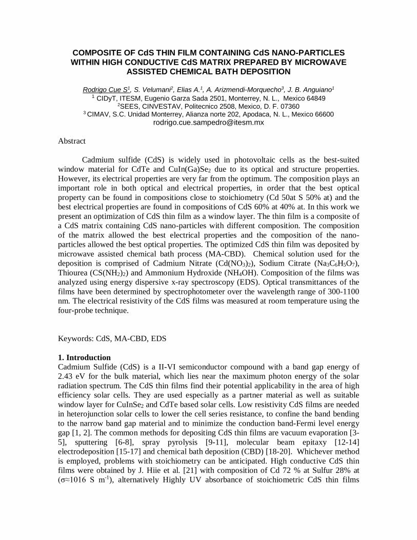
Figure 1. SEM image of 120 nm film with amplification of 40,000X
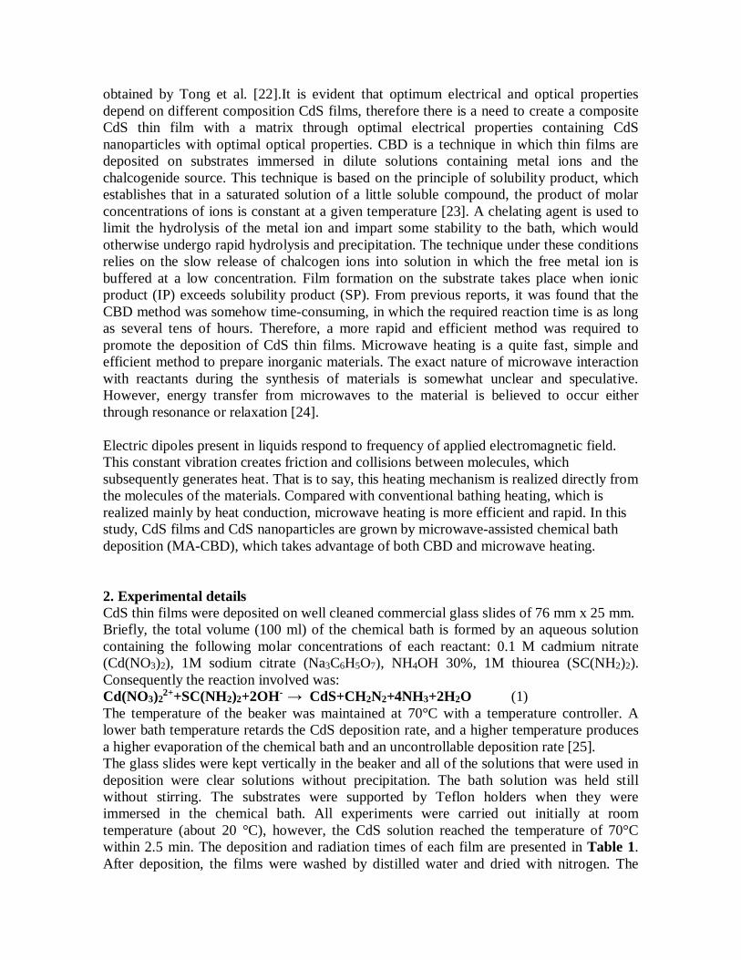
3. Results and discussion MA-CBD CdS thin films were studied by SEM. Figure 1 shows the morphology of the 120 nm thickness CdS thin film, it can be seen that CdS particles are homogeneously dispersed in the film. EDS analysis shows that the composition of the film is: Sulfur 30.37% at and Cadmium 69.63% at (Figure 2-a). This low sulfur content allows conductivity to increase.
Figure 2 Energy Dispersive X-ray Spectroscopy of the matrix a) and naonparticles b) of 120 nm MA-CBD
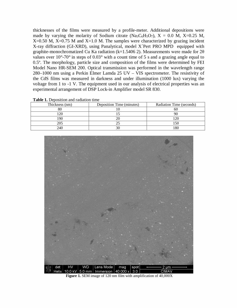
CdS thin film The magnification of the particles shows that each particle that appears in Figure 1 is actually an agglomerate of several nanoparticles as it can be seen in Figure 3. The composition of the nanoparticles is: Sulfur 42.17% at and Cadmium 57.83 % at (Figure 2-b).
Figure 3. SEM image of the nanoparticles of CdS thin film with 120 nm thickness
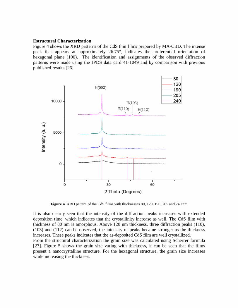
Estructural Characterization Figure 4 shows the XRD patterns of the CdS thin films prepared by MA-CBD. The intense peak that appears at approximately 26.75°, indicates the preferential orientation of hexagonal plane (100). The identification and assignments of the observed diffraction patterns were made using the JPDS data card 41-1049 and by comparison with previous published results [26].
Figure 4. XRD pattern of the CdS films with thicknesses 80, 120, 190, 205 and 240 nm
It is also clearly seen that the intensity of the diffraction peaks increases with extended deposition time, which indicates that the crystallinity increase as well. The CdS film with thickness of 80 nm is amorphous. Above 120 nm thickness, three diffraction peaks (110), (103) and (112) can be observed, the intensity of peaks became stronger as the thickness increases. These peaks indicates that the as-deposited CdS film are well crystallized. From the structural characterization the grain size was calculated using Scherrer formula [27]. Figure 5 shows the grain size varing with thickness, it can be seen that the films present a nanocrystalline structure. For the hexagonal structure, the grain size increases while increasing the thickness.
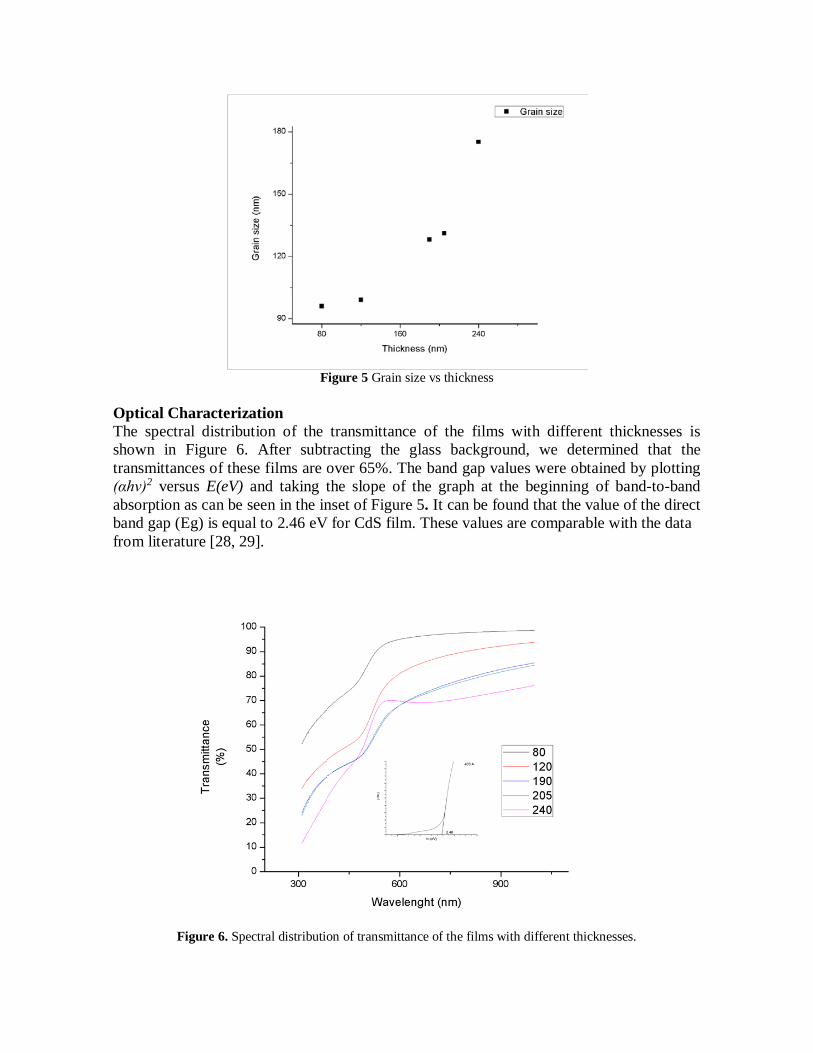
Figure 5 Grain size vs thickness
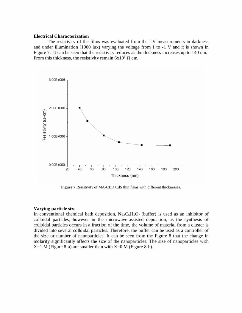
Optical Characterization The spectral distribution of the transmittance of the films with different thicknesses is shown in Figure 6. After subtracting the glass background, we determined that the transmittances of these films are over 65%. The band gap values were obtained by plotting (αhν)2 versus E(eV) and taking the slope of the graph at the beginning of band-to-band absorption as can be seen in the inset of Figure 5. It can be found that the value of the direct band gap (Eg) is equal to 2.46 eV for CdS film. These values are comparable with the data from literature [28, 29].
Figure 6. Spectral distribution of transmittance of the films with different thicknesses.
Electrical Characterization
The resistivity of the films was evaluated from the I-V measurements in darkness and under illumination (1000 lux) varying the voltage from 1 to -1 V and it is shown in Figure 7. It can be seen that the resistivity reduces as the thickness increases up to 140 nm. From this thickness, the resistivity remain 6x10⁵ Ω cm.
Figure 7 Resistivity of MA-CBD CdS thin films with different thicknesses.
Varying particle size In conventional chemical bath deposition, Na3C6H5O7 (buffer) is used as an inhibitor of colloidal particles, however in the microwave-assisted deposition, as the synthesis of colloidal particles occurs in a fraction of the time, the volume of material from a cluster is divided into several colloidal particles. Therefore, the buffer can be used as a controller of the size or number of nanoparticles. It can be seen from the Figure 8 that the change in molarity significantly affects the size of the nanoparticles. The size of nanoparticles with X=1 M (Figure 8-a) are smaller than with X=0 M (Figure 8-b).
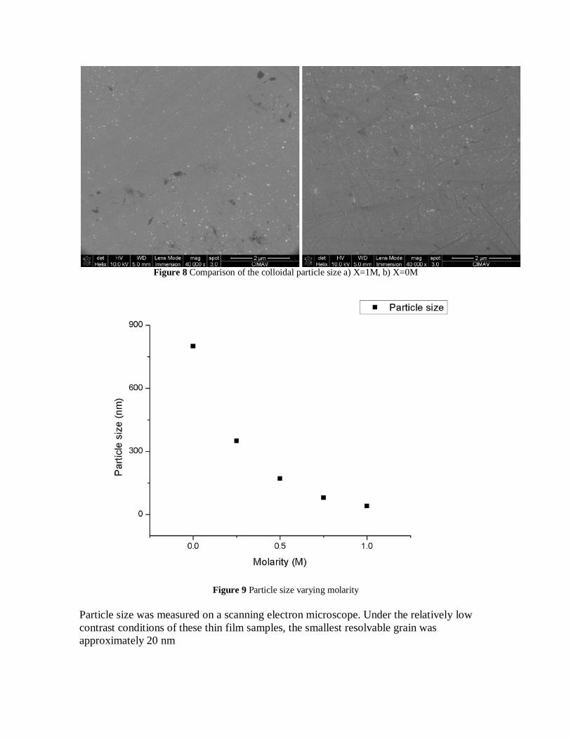
Figure 8 Comparison of the colloidal particle size a) X=1M, b) X=0M
Figure 9 Particle size varying molarity
Particle size was measured on a scanning electron microscope. Under the relatively low contrast conditions of these thin film samples, the smallest resolvable grain was approximately 20 nm
Conclusions MA-CBD of CdS is investigated in this work. Both nanoparticles and thin film can be synthesized in by this technique. The CdS thin film obtain was crystalline in nature mainly with hexagonal structure. The EDS analysis show that the composition of the CdS nanoparticles improve the optical band gap from 2.43 eV to 2.46 eV and the CdS thin film has optimal conductivity of . A direct relationship with the molarity of the buffer and particle size was observed. With molarity of X= 0 M the particle size was of 198 nm and for X=1M, 60 nm. Thus the particle size reduces as the buffer concentration increases. This advantage have appropriate properties that benefit directly the Solar Cells field. Acknowledgements The work carried out at CIDyT-ITESM has been supported by CONACYT-61061. The authors also like to thank CINVESTAV and CIMAV for their useful help during this work. References [1] Jae-Hyeong Lee, Jun-Sin Yi, Kea-Joon Yang, Joon-Hoon Park and Ryum-Duk Oh,
Thin Solid Films 431-432 (2003) 344-348 [2] A. E. Rakhshani, A. S. Al-Azab, J. Phys. Condens. Matter 12 (2000) 8745 [3] Zhibing He, Gaoling Zhao, Wenjian Weng, Piyi Du, Ge Shen, Gaorong Han,
Vacuum 79, (2005) 14-18 [4] Jae-Hyeong Lee, Dong-Gun Lim and Jun-Sin Yi, Solar Energy Materials & Solar
Cells 75, (2003) 235-242 [5] K. Senthil, D. Mangalaraj et al, Physica B 304 (2001) 175-180. [6] Jae-Hyeong lee and Dong-Jin Lee, Thin Solid Films 515 (2007) 6055-6059. [7] P. K. Ghosh, U. N. Maiti and K. K. Chattopadhyay, Materials Letters 60 (2006)
2881-2885. [8] Byung-Sik Moon, Jae-Hyeong Lee , Hakkee Jung, Thin Solid Films vol. 511 – 512,
(2006) 299 – 303 [9] J. Hiie, T. Dedova, V. Valdna and K. Muska, Thin Solid Films 511-512 (2006) 443-
447. [10] V. Krishna Kumar, K. Ramamurthi and E. Elangovan, Solid State Communications
132 (2004) 673-677. [11] F. Atay, S. Kose, V. Bilgin and I. Akyuz, Materials Letters 57 (2003) 3461-3472. [12] Joo Won Choi, A. Bhupathiraju, M. A. Hasan and John M. Lannon, Crystal Growth
255 (2003) 1-7 [13] S. Petillon, A. dinger et al, Crystal Growth 201-202 (1999) 457-460. [14] A. Dinger et al, Crystal F¡Growth 200 (1999) 391-398. [15] Wenbin Yang et al, Microelectronic Engineering 83 (2006) 1971-1974. [16] K. Premaratne et al, Renewable Energy 29 (2003) 549-557. [17] N. W. Duffy, D. Lane, M. E. Ôzsan, L. M. Peter, K. D. Rogers and R. L. Wang,
Thin Solid Film 361-362 (2000) 314-320. [18] Joel Pantoja Enriquez, Xavier Mathew, Solar Energy Materiasl & Solar Cells 76
(2003) 313-322
[19] G. Sasikala, P. Thilakan, C. Subramanian, Sol. Energy Mater. Sol. Cells 62, (2000) 275
[20] K. S. Ramaiah, R. D. Pilkington, A. E. Hill, R. D. Tomlinson, A. K. Bhatnagar, Materials Chemistry and Physics 68, (2001) 22
[21] J. Hiie, T. Dedova, V. Valdna, K. Muska, Thin Solid Films 511 – 512 (2006) 443 – 447
[22] X.L. Tong, D. S. Jiang, L. Liu, Z. M. Liu, M. Z. Luo, Optics Communications 270 (2007) 356–360
[23] Jorge G Ibañez, Flora Gomez, Ivonne Konik, Diane E Lozano, et al, Journal of Chemical Education, 74, 10, (1997) 1205
[24] Ran Zhai, ShuBo Wang, Hai Yan Xu, Hao Wang, Hui Yan, Materials Letters 59 (2005) 14
[25] P.J. Sebastian, H. Hu, Advanced Materials for Optical Electronics, 4 (1994) 407 [26] Rodrigo Cue S., S. Velumani, P. J. Sebastian, J. A. Chavez-Carvayar, New
Materials for Electrochemical Systems 13, (2010) 7-14 [27] Donald R. Askeland, Science and Engineering of Materials, third edition,
Wadsworth Publishing Company, Boston 1994, p. 68 [28] M.B. Ortuño-López, M. Sotelo-Lerma, A. Mendoza-Galván, R. Ramírez-Bon,
Vacuum 76 (2004) 181–184 [29] A.I. Oliva, O. Solís-Canto, R. Castro-Rodríguez, P. Quintana, Thin Solid Films 391
(2001) 28-35