chapter 4 solutions - elsevier
TRANSCRIPT

Solutions
4
Chapter 4 Solutions S-3
4.1
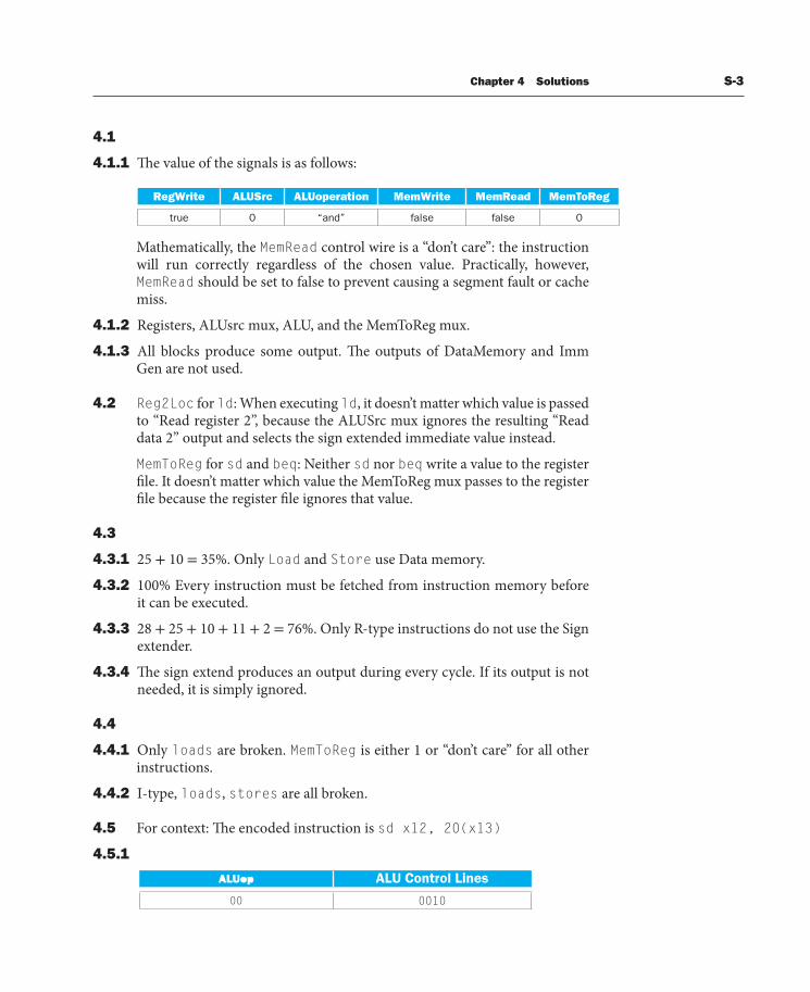
4.1.1 Th e value of the signals is as follows:
Mathematically, the MemRead control wire is a “don’t care”: the instruction will run correctly regardless of the chosen value. Practically, however, MemRead should be set to false to prevent causing a segment fault or cache miss.
4.1.2 Registers, ALUsrc mux, ALU, and the MemToReg mux.
4.1.3 All blocks produce some output. Th e outputs of DataMemory and Imm Gen are not used.
4.2 Reg2Loc for ld : When executing ld , it doesn’t matter which value is passed to “Read register 2”, because the ALUSrc mux ignores the resulting “Read data 2” output and selects the sign extended immediate value instead.
MemToReg for sd and beq : Neither sd nor beq write a value to the register fi le. It doesn’t matter which value the MemToReg mux passes to the register fi le because the register fi le ignores that value.
4.3
4.3.1 25 + 10 = 35%. Only Load and Store use Data memory.
4.3.2 100% Every instruction must be fetched from instruction memory before it can be executed.
4.3.3 28 + 25 + 10 + 11 + 2 = 76%. Only R-type instructions do not use the Sign extender.
4.3.4 Th e sign extend produces an output during every cycle. If its output is not needed, it is simply ignored.
4.4
4.4.1 Only loads are broken. MemToReg is either 1 or “don’t care” for all other instructions.
4.4.2 I-type, loads , stores are all broken.
4.5 For context: Th e encoded instruction is sd x12, 20(x13)
4.5.1
S-4 Chapter 4 Solutions
4.5.2 Th e new PC is the old PC + 4. Th is signal goes from the PC, through the “PC + 4” adder, through the “branch” mux, and back to the PC.
4.5.3 ALUsrc : Inputs: Reg[x12] and 0x0000000000000014 ; Output: 0x0000000000000014
MemToReg : Inputs: Reg[x13] + 0x14 and <undefined> ; output: <undefined>
Branch: Inputs: PC+4 and 0x000000000000000A
4.5.4 ALU inputs: Reg[x13] and 0x0000000000000014
PC + 4 adder inputs: PC and 4
Branch adder inputs: PC and 0x0000000000000028
4.6
4.6.1 No additional logic blocks are needed.
4.6.2 Branch: false MemRead: false (See footnote from solution to problem 4.1.1.) MemToReg: 0 ALUop: 10 (or simply saying “add” is suffi cient for this problem) MemWrite: false ALUsrc: 1 RegWrite: 1
4.7
4.7.1 R-type : 30 + 250 + 150 + 25 + 200 + 25 + 20 = 700ps
4.7.2 ld : 30 + 250 + 150 + 25 + 200 + 250 + 25 + 20 = 950 ps
4.7.3 sd : 30 + 250 + 150 + 200 + 25 + 250 = 905
4.7.4 beq : 30 + 250 + 150 + 25 + 200 + 5 + 25 + 20 = 705
4.7.5 I-type : 30 + 250 + 150 + 25 + 200 + 25 + 20 = 700ps
Chapter 4 Solutions S-5
4.7.6 950ps
4.8 Using the results from Problem 4.7, we see that the average time per instruction is
.52*700 + .25*950 + .11*905 + .12 * 705 = 785.6ps
In contrast, a single-cycle CPU with a “normal” clock would require a clock cycle time of 950.
Th us, the speedup would be 925/787.6 = 1.174
4.9
4.9.1 Without improvement: 950; With improvement: 1250
4.9.2 Th e running time of a program on the original CPU is 950*n. Th e running time on the improved CPU is 1250*(0.95)*n = 1187.5. Th us, the “speedup” is 0.8. (Th us, this “improved” CPU is actually slower than the original).
4.9.3 Because adding a multiply instruction will remove 5% of the instructions, the cycle time can grow to as much as 950/(0.95) = 1000. Th us, the time for the ALU can increase by up to 50 (from 200 to 250).
4.10
4.10.1 Th e additional registers will allow us to remove 12% of the loads and stores, or (0.12)*(0.25 + 0.1) = 4.2% of all instructions. Th us, the time to run n instructions will decrease from 950*n to 960*.958*n = 919.68*n. Th at corresponds to a speedup of 950/895.73 = 1.03.
4.10.2 Th e cost of the original CPU is 4507; the cost of the improved CPU is 4707.
PC: 5 I-Mem: 1000 Register fi le: 200 ALU: 100 D-Mem: 2000 Sign Extend: 1002 Controls: 10002 adders: 30*24 muxes: 4*102 single gates: 2*1
Th us, for a 3% increase in performance, the cost of the CPU increases by about 4.4%.
S-6 Chapter 4 Solutions
4.10.3 From a strictly mathematical standpoint it does not make sense to add more registers because the new CPU costs more per unit of performance. However, that simple calculation does not account for the utility of the performance. For example, in a real-time system, a 3% performance may make the diff erence between meeting or missing deadlines. In which case, the improvement would be well worth the 4.4% additional cost.
4.11
4.11.1 No new functional blocks are needed.
4.11.2 Only the control unit needs modifi cation.
4.11.3 No new data paths are needed.
4.11.4 No new signals are needed.
4.12
4.12.1 No new functional blocks are needed.
4.12.2 Th e register fi le needs to be modifi ed so that it can write to two registers in the same cycle. Th e ALU would also need to be modifi ed to allow read data 1 or 2 to be passed through to write data 1.
4.12.3 Th e answer depends on the answer given in 4.12.2: whichever input was not allowed to pass through the ALU above must now have a data path to write data 2.
4.12.4 Th ere would need to be a second RegWrite control wire.
4.12.5 Many possible solutions.
4.13
4.13.1 We need some additional muxes to drive the data paths discussed in 4.13.3.
4.13.2 No functional blocks need to be modifi ed.
4.13.3 Th ere needs to be a path from the ALU output to data memory’s write data port. Th ere also needs to be a path from read data 2 directly to Data memory’s Address input.
4.13.4 Th ese new data paths will need to be driven by muxes. Th ese muxes will require control wires for the selector.
4.13.5 Many possible solutions.
Chapter 4 Solutions S-7
4.14 None: all instructions that use sign extend also use the register fi le, which is slower.
4.15
4.15.1 Th e new clock cycle time would be 750. ALU and Data Memory will now run in parallel, so we have eff ectively removed the faster of the two (the ALU with time 200) from the critical path.
4.15.2 Slower. Th e original CPU takes 950*n picoseconds to run n instructions. Th e same program will have approximately 1.35*n instructions when compiled for the new machine. Th us, the time on the new machine will be 750*1.35n = 1012.5*n. Th is represents a “speedup” of .93.
4.15.3 Th e number of loads and stores is the primary factor. How the loads and stores are used can also have an eff ect. For example, a program whose loads and stores tend to be to only a few diff erent address may also run faster on the new machine.
4.15.4 Th is answer is a matter of opinion.
4.16
4.16.1 Pipelined: 350; non-pipelined: 1250
4.16.2 Pipelined: 1250; non-pipelined: 1250
4.16.3 Split the ID stage. Th is reduces the clock-cycle time to 300ps.
4.16.4 35%.
4.16.5 65%
4.17 n + k − 1. Let’s look at when each instruction is in the WB stage. In a k-stage pipeline, the 1st instruction doesn’t enter the WB stage until cycle k. From that point on, at most one of the remaining n − 1 instructions is in the WB stage during every cycle.
Th is gives us a minimum of k + (n − 1) = n + k − 1 cycles.
4.18 x13 = 33 and x14 = 36
4.19 x15 = 54 (Th e code will run correctly because the result of the fi rst instruction is written back to the register fi le at the beginning of the 5th cycle, whereas the fi nal instruction reads the updated value of x1 during the second half of this cycle.)
S-8 Chapter 4 Solutions
4.20 addi x11, x12, 5 NOP NOP add x13, x11, x12 addi x14, x11, 15 NOP add x15, x13, x12
4.21
4.21.1 Pipeline without forwarding requires 1.4*n*250ps. Pipeline with forwarding requires 1.05*n*300ps. Th e speedup is therefore (1.4*250)/(1.05*300) = 1.11.
4.21.2 Our goal is for the pipeline with forwarding to be faster than the pipeline without forwarding. Let y be the number of stalls remaining as a percentage of “code” instructions. Our goal is for 300*(1+y)*n < 250*1.4*n. Th us, y must be less than 16.7%.
4.21.3 Th is time, our goal is for 300(1 + y)*n < 250(1 + x)*n. Th is happens when y < (250x − 50)/300.
4.21.4 It cannot. In the best case, where forwarding eliminates the need for every NOP, the program will take time 300*n to run on the pipeline with forwarding. Th is is slower than the 250*1.075*n required on the pipeline with no forwarding.
4.21.5 Speedup is not possible when the solution to 4.21.3 is less than 0. Solving 0< (250x − 50)/300 for x gives that x must be at least 0.2.
4.22
4.22.1 Stalls are marked with **:
sd x29, 12(x16) IF ID EX ME WB ld x29, 8(x16) IF ID EX ME WB sub x17, x15, x14 IF ID EX ME WB bez x17, label ** ** IF ID EX ME WB add x15, x11, x14 IF ID EX ME WB sub x15,x30,x14 IF ID EX ME WB
4.22.2 Reordering code won’t help. Every instruction must be fetched; thus, every data access causes a stall. Reordering code will just change the pair of instructions that are in confl ict.
Chapter 4 Solutions S-9
4.22.3 You can’t solve this structural hazard with NOPs, because even the NOPs must be fetched from instruction memory.
4.22.4 35%. Every data access will cause a stall.
4.23
4.23.1 Th e clock period won’t change because we aren’t making any changes to the slowest stage.
4.23.2 Moving the MEM stage in parallel with the EX stage will eliminate the need for a cycle between loads and operations that use the result of the loads. Th is can potentially reduce the number of stalls in a program.
4.23.3 Removing the off set from ld and sd may increase the total number of instructions because some ld and sd instructions will need to be replaced with a addi/ld or addi/sd pair.
4.24 Th e second one. A careful examination of Figure 4.59 shows that the need for a stall is detected during the ID stage. It is this stage that prevents the fetch of a new instruction, eff ectively causing the add to repeat its ID stage.
4.25
4.25.1 … indicates a stall. ! indicates a stage that does not do useful work.
ld x10, 0(x13) IF ID EX ME | WB ld x11, 8(x13) IF ID EX | ME WB add x12, x10, x11 IF ID | .. EX ME! WB addi x13, x13, -16 IF | .. ID EX ME! WB bnez x12, LOOP | .. IF ID EX ME! WB! ld x10, 0(x13) IF ID EX ME WB ld x11, 8(x13) IF ID EX ME WB add x12, x10, x11 IF ID .. EX | ME! WB addi x13, x13, -16 IF .. ID | EX ME! WB bnez x12, LOOP IF | ID EX ME! WB! Completely busy | N N N N N N N N |
4.25.2 In a particular clock cycle, a pipeline stage is not doing useful work if it is stalled or if the instruction going through that stage is not doing any useful work there. As the diagram above shows, there are not any cycles during which every pipeline stage is doing useful work.
S-10 Chapter 4 Solutions
4.26
4.26.1 // EX to 1st only: add x11, x12, x13 add x14, x11, x15 add x5, x6, x7
// MEM to 1st only: ld x11, 0(x12) add x15, x11, x13 add x5, x6, x7
// EX to 2nd only: add x11, x12, x13 add x5, x6, x7 add x14, x11, x12
// MEM to 2nd only: ld x11, 0(x12) add x5, x6, x7 add x14, x11, x13
// EX to 1st and EX to 2nd: add x11, x12, x13 add x5, x11, x15 add x16, x11, x12
4.26.2 // EX to 1st only: 2 nops add x11, x12, x13 nop nop add x14, x11, x15 add x5, x6, x7
// MEM to 1st only: 2 stalls ld x11, 0(x12) nop nop add x15, x11, x13 add x5, x6, x7
// EX to 2nd only: 1 nop add x11, x12, x13 add x5, x6, x7 nop add x14, x11, x12
Chapter 4 Solutions S-11
// MEM to 2nd only: 1 nop ld x11, 0(x12) add x5, x6, x7 nop add x14, x11, x13
// EX to 1st and EX to 2nd: 2 nops add x11, x12, x13 nop nop add x5, x11, x15 add x16, x11, x12
4.26.3 Consider this code:
ld x11, 0(x5) # MEM to 2nd --- one stall add x12, x6, x7 # EX to 1st --- two stalls add x13, x11, x12 add x28, x29, x30
If we analyze each instruction separately, we would calculate that we need to add 3 stalls (one for a “MEM to 2nd” and two for an “EX to 1st only”. However, as we can see below, we need only two stalls:
ld x11, 0(x5) add x12, x6, x7 nop nop add x13, x11, x12 add x28, x29, x30
4.26.4 Taking a weighted average of the answers from 4.26.2 gives 0.05*2 + 0.2*2 + 0.05*1 + 0.1*1 + 0.1*2 = 0.85 stalls per instruction (on average) for a CPI of 1.85. Th is means that 0.85/1.85 cycles, or 46%, are stalls.
4.26.5 Th e only dependency that cannot be handled by forwarding is from the MEM stage to the next instruction. Th us, 20% of instructions will generate one stall for a CPI of 1.2. Th is means that 0.2 out of 1.2 cycles, or 17%, are stalls.
4.26.6 If we forward from the EX/MEM register only, we have the following stalls/NOPs
EX to 1st: 0 MEM to 1st: 2 EX to 2nd: 1 MEM to 2nd: 1 EX to 1st and 2nd: 1
S-12 Chapter 4 Solutions
Th is represents an average of 0.05*0 + 0.2*2 + 0.05*1 + 0.10*1 + 0.10*1 = 0.65 stalls/instruction. Th us, the CPI is 1.65
IF we forward from MEM/WB only, we have the following stalls/NOPs
EX to 1st: 1 MEM to 1st: 1 EX to 2nd: 0 MEM to 2nd: 0 EX to 1st and 2nd: 1
Th is represents an average of 0.05*1 + 0.2*1 + 0.1*1 = 0.35 stalls/instruction. Th us, the CPI is 1.35.
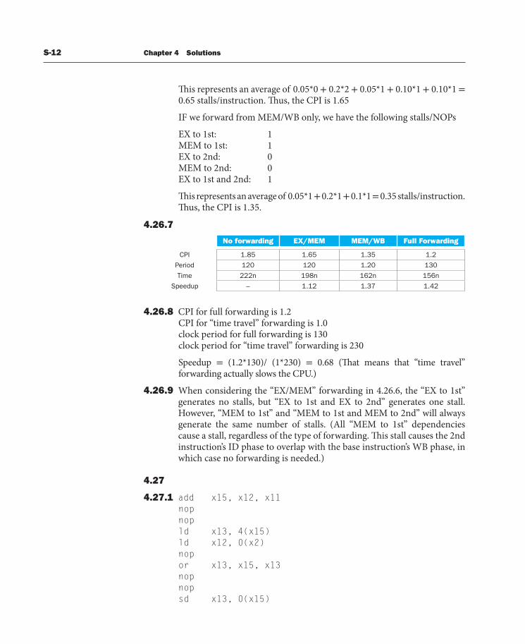
4.26.7
4.26.8 CPI for full forwarding is 1.2
CPI for “time travel” forwarding is 1.0 clock period for full forwarding is 130 clock period for “time travel” forwarding is 230
Speedup = (1.2*130)/ (1*230) = 0.68 (Th at means that “time travel” forwarding actually slows the CPU.)
4.26.9 When considering the “EX/MEM” forwarding in 4.26.6, the “EX to 1st” generates no stalls, but “EX to 1st and EX to 2nd” generates one stall. However, “MEM to 1st” and “MEM to 1st and MEM to 2nd” will always generate the same number of stalls. (All “MEM to 1st” dependencies cause a stall, regardless of the type of forwarding. Th is stall causes the 2nd instruction’s ID phase to overlap with the base instruction’s WB phase, in which case no forwarding is needed.)
4.27
4.27.1 add x15, x12, x11 nop nop ld x13, 4(x15) ld x12, 0(x2) nop or x13, x15, x13 nop nop sd x13, 0(x15)
Chapter 4 Solutions S-13
4.27.2 It is not possible to reduce the number of NOPs.
4.27.3 Th e code executes correctly. We need hazard detection only to insert a stall when the instruction following a load uses the result of the load. Th at does not happen in this case.
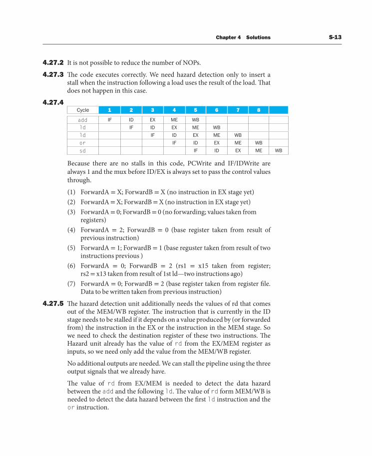
4.27.4
Because there are no stalls in this code, PCWrite and IF/IDWrite are always 1 and the mux before ID/EX is always set to pass the control values through.
(1) ForwardA = X; ForwardB = X (no instruction in EX stage yet) (2) ForwardA = X; ForwardB = X (no instruction in EX stage yet) (3) ForwardA = 0; ForwardB = 0 (no forwarding; values taken from
registers) (4) ForwardA = 2; ForwardB = 0 (base register taken from result of
previous instruction) (5) ForwardA = 1; ForwardB = 1 (base reguster taken from result of two
instructions previous ) (6) ForwardA = 0; ForwardB = 2 (rs1 = x15 taken from register;
rs2 = x13 taken from result of 1st ld—two instructions ago) (7) ForwardA = 0; ForwardB = 2 (base register taken from register fi le.
Data to be written taken from previous instruction)
4.27.5 Th e hazard detection unit additionally needs the values of rd that comes out of the MEM/WB register. Th e instruction that is currently in the ID stage needs to be stalled if it depends on a value produced by (or forwarded from) the instruction in the EX or the instruction in the MEM stage. So we need to check the destination register of these two instructions. Th e Hazard unit already has the value of rd from the EX/MEM register as inputs, so we need only add the value from the MEM/WB register.
No additional outputs are needed. We can stall the pipeline using the three output signals that we already have.
Th e value of rd from EX/MEM is needed to detect the data hazard between the add and the following ld . Th e value of rd form MEM/WB is needed to detect the data hazard between the fi rst ld instruction and the or instruction.
S-14 Chapter 4 Solutions
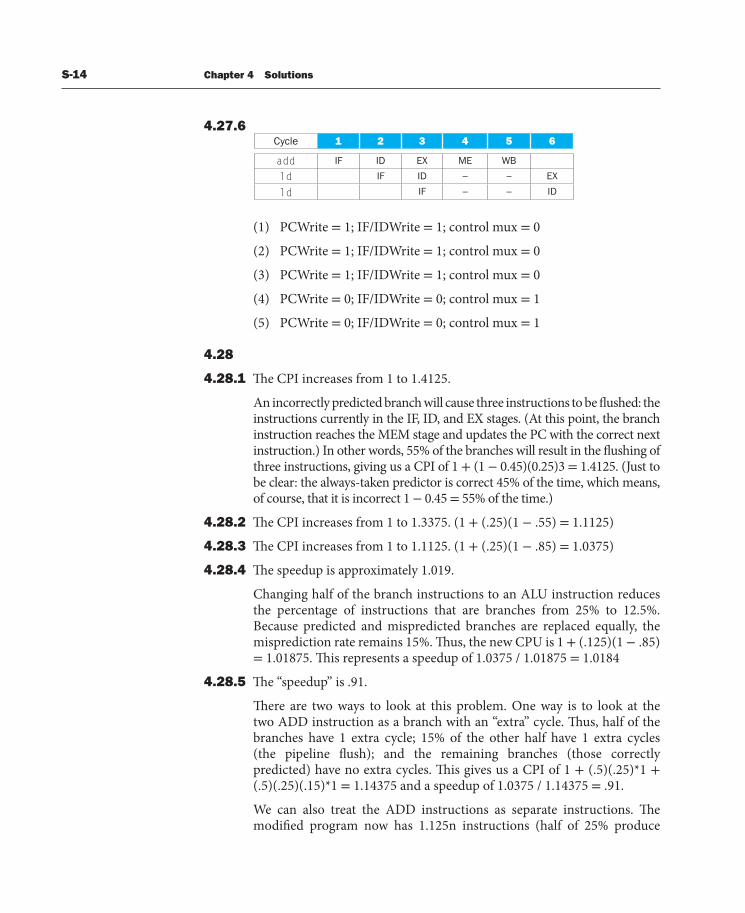
4.27.6
(1) PCWrite = 1; IF/IDWrite = 1; control mux = 0
(2) PCWrite = 1; IF/IDWrite = 1; control mux = 0
(3) PCWrite = 1; IF/IDWrite = 1; control mux = 0
(4) PCWrite = 0; IF/IDWrite = 0; control mux = 1
(5) PCWrite = 0; IF/IDWrite = 0; control mux = 1
4.28
4.28.1 Th e CPI increases from 1 to 1.4125.
An incorrectly predicted branch will cause three instructions to be fl ushed: the instructions currently in the IF, ID, and EX stages. (At this point, the branch instruction reaches the MEM stage and updates the PC with the correct next instruction.) In other words, 55% of the branches will result in the fl ushing of three instructions, giving us a CPI of 1 + (1 − 0.45)(0.25)3 = 1.4125. (Just to be clear: the always-taken predictor is correct 45% of the time, which means, of course, that it is incorrect 1 − 0.45 = 55% of the time.)
4.28.2 Th e CPI increases from 1 to 1.3375. (1 + (.25)(1 − .55) = 1.1125)
4.28.3 Th e CPI increases from 1 to 1.1125. (1 + (.25)(1 − .85) = 1.0375)
4.28.4 Th e speedup is approximately 1.019.
Changing half of the branch instructions to an ALU instruction reduces the percentage of instructions that are branches from 25% to 12.5%. Because predicted and mispredicted branches are replaced equally, the misprediction rate remains 15%. Th us, the new CPU is 1 + (.125)(1 − .85) = 1.01875. Th is represents a speedup of 1.0375 / 1.01875 = 1.0184
4.28.5 Th e “speedup” is .91.
Th ere are two ways to look at this problem. One way is to look at the two ADD instruction as a branch with an “extra” cycle. Th us, half of the branches have 1 extra cycle; 15% of the other half have 1 extra cycles (the pipeline fl ush); and the remaining branches (those correctly predicted) have no extra cycles. Th is gives us a CPI of 1 + (.5)(.25)*1 + (.5)(.25)(.15)*1 = 1.14375 and a speedup of 1.0375 / 1.14375 = .91.
We can also treat the ADD instructions as separate instructions. Th e modifi ed program now has 1.125n instructions (half of 25% produce
Chapter 4 Solutions S-15
an extra instruction). .125n of these 1.125n instruction (or 11.1%) are branches. Th e CPI for this new program is 1 + (.111)(.15)*1 = 1.01665. When we factor in the 12.5% increase in instructions, we get a speedup of 1.0375 / (1.125 * 1.01665) = .91.
4.28.6 Th e predictor is 25% accurate on the remaining branches. We know that 80% of branches are always predicted correctly and the overall accuracy is 0.85. Th us, 0.8*1 + 0.2*x = 0.85. Solving for x shows that x = 0.25.
4.29
4.29.1
4.29.2
4.29.3 Th e fi rst few recurrences of this pattern do not have the same accuracy as the later ones because the predictor is still warming up. To determine the accuracy in the “steady state”, we must work through the branch predictions until the predictor values start repeating (i.e. until the predictor has the same value at the start of the current and the next recurrence of the pattern).
4.29.4 Th e predictor should be an N-bit shift register, where N is the number of branch outcomes in the target pattern. Th e shift register should be initialized with the pattern itself (0 for NT, 1 for T), and the prediction is always the value in the left most bit of the shift register. Th e register should be shift ed aft er each predicted branch.
4.29.5 Since the predictor’s output is always the opposite of the actual outcome of the branch instruction, the accuracy is zero.
4.29.6 Th e predictor is the same as in part d, except that it should compare its prediction to the actual outcome and invert (logical NOT) all the bits in the shift register if the prediction is incorrect. Th is predictor still always perfectly predicts the given pattern. For the opposite pattern, the fi rst prediction will be incorrect, so the predictor’s state is inverted and aft er
S-16 Chapter 4 Solutions
that the predictions are always correct. Overall, there is no warm-up period for the given pattern, and the warm-up period for the opposite pattern is only one branch.
4.30
4.30.1
4.30.2 Th e Mux that selects the next PC must have inputs added to it. Each input is a constant address of an exception handler. Th e exception detectors must be added to the appropriate pipeline stage and the outputs of these detectors must be used to control the pre-PC Mux, and also to convert to NOPs instructions that are already in the pipeline behind the exception-triggering instruction.
4.30.3 Instructions are fetched normally until the exception is detected. When the exception is detected, all instructions that are in the pipeline aft er the fi rst instruction must be converted to NOPs. As a result, the second instruction never completes and does not aff ect pipeline state. In the cycle that immediately follows the cycle in which the exception is detected, the processor will fetch the fi rst instruction of the exception handler.
4.30.4 Th is approach requires us to fetch the address of the handler from memory. We must add the code of the exception to the address of the exception vector table, read the handler’s address from memory, and jump to that address. One way of doing this is to handle it like a special instruction that puts the address in EX, loads the handler’s address in MEM, and sets the PC in WB.
4.30.5 We need a special instruction that allows us to move a value from the (exception) Cause register to a general-purpose register. We must fi rst save the general-purpose register (so we can restore it later), load the Cause register into it, add the address of the vector table to it, use the result as an address for a load that gets the address of the right exception handler from memory, and fi nally jump to that handler.
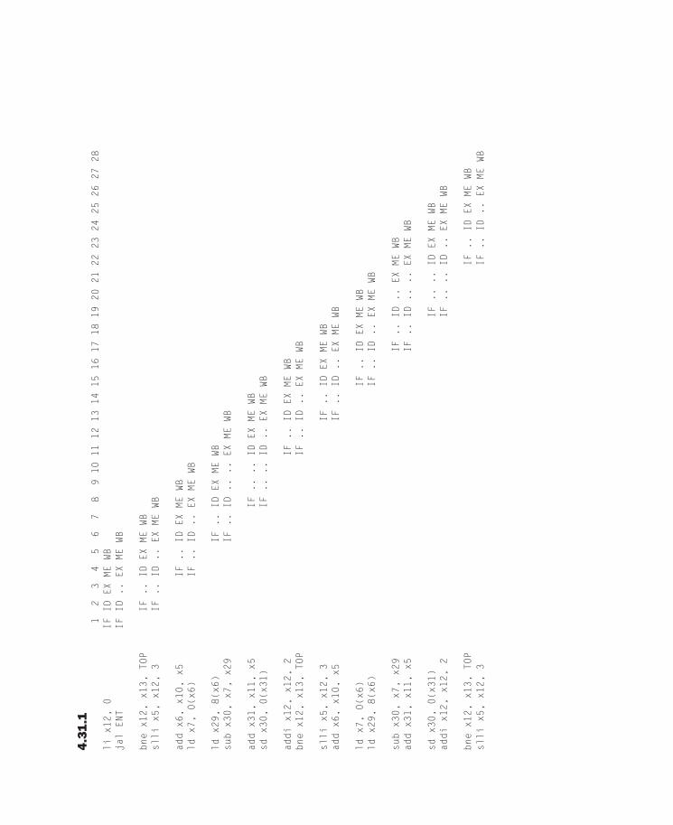
4.3
1.1
1 2
3 4
5 6
7 8
9
10 11 12 13 14 15 16 17 18 19 20 21 22 23 24 25 26 27 28
li x
12,
0
IF
ID E
X ME
WB
jal
ENT
IF
ID .
. EX
ME
WB
bne
x12,
x13
, TO
P
IF .
. ID
EX
ME WB
slli
x5,
x12
, 3
IF .
. ID
..
EX ME WB
add
x6,
x10,
x5
IF .
. ID EX ME WB
ld x
7, 0
(x6)
IF .
. ID .. EX ME WB
ld x
29,
8(x6
)
IF .. ID EX ME WB
sub
x30,
x7,
x29
IF .. ID .. .. EX ME WB
add
x31,
x11
, x5
IF .. .. ID EX ME WB
sd x
30,
0(x3
1)
IF .. .. ID .. EX ME WB
addi
x12
, x1
2, 2
IF .. ID EX ME WB
bne
x12,
x13
, TO
P
IF .. ID .. EX ME WB
slli
x5,
x12
, 3
IF .. ID EX ME WB
add
x6,
x10,
x5
IF .. ID .. EX ME WB
ld x
7, 0
(x6)
IF .. ID EX ME WB
ld x
29,
8(x6
)
IF .. ID .. EX ME WB
sub
x30,
x7,
x29
IF .. ID .. EX ME WB
add
x31,
x11
, x5
IF .. ID .. .. EX ME WB
sd x
30,
0(x3
1)
IF .. .. ID EX ME WB
addi
x12
, x1
2, 2
IF .. .. ID .. EX ME WB
bne
x12,
x13
, TO
P
IF .. ID EX ME WB
slli
x5,
x12
, 3
IF .. ID .. EX ME WB
S-18 Chapter 4 Solutions
4.31.2 Th e original code requires 10 cycles/loop on a 1-issue machine (stalls shown below) and 10 cycles/loop on the 2-issue machine. Th is gives no net speedup. (Th at’s a terrible result considering we nearly doubled the amount of hardware.) We know that the code takes 10 cycles/iteration on the 2-issue machine because the fi rst instruction in loop 1 (Th e slli) begins execution in cycle 6 and the fi rst instruction in iteration 3 begins execution in cycle 26, so (26–6)/2 = 10.
li x12,0 jal ENT
TOP: slli x5, x12, 3 add x6, x10, x5 ld x7, 0(x6) ld x29, 8(x6) <stall> sub x30, x7, x29 add x31, x11, x5 sd x30, 0(x31) addi x12, x12, 2
ENT: bne x12, x13, TOP
4.31.3 Here is one possibility:
beqz x13, DONE li x12, 0 jal ENT
TOP: slli x5, x12, 3 add x6, x10, x5 ld x7, 0(x6) ld x29, 8(x6) addi x12, x12, 2 sub x30, x7, x29 add x31, x11, x5 sd x30, 0(x31)
ENT: bne x12, x13, TOP
DONE:
If we switch to a “pointer-based” approach, we can save one cycle/loop.
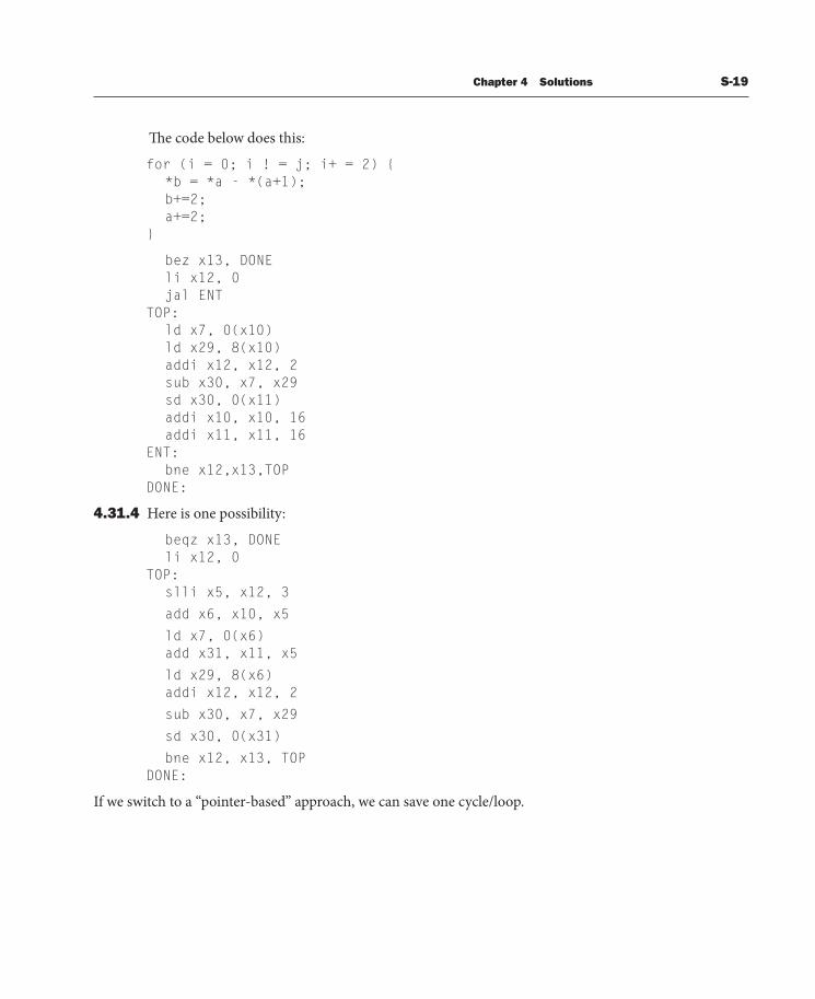
Chapter 4 Solutions S-19
Th e code below does this:
for (i = 0; i ! = j; i+ = 2) { *b = *a - *(a+1); b+=2; a+=2;
}
bez x13, DONE li x12, 0 jal ENT
TOP: ld x7, 0(x10) ld x29, 8(x10) addi x12, x12, 2 sub x30, x7, x29 sd x30, 0(x11) addi x10, x10, 16 addi x11, x11, 16
ENT: bne x12,x13,TOP
DONE:
4.31.4 Here is one possibility:
beqz x13, DONE li x12, 0
TOP: slli x5, x12, 3
add x6, x10, x5
ld x7, 0(x6) add x31, x11, x5
ld x29, 8(x6) addi x12, x12, 2
sub x30, x7, x29
sd x30, 0(x31)
bne x12, x13, TOP DONE:
If we switch to a “pointer-based” approach, we can save one cycle/loop.
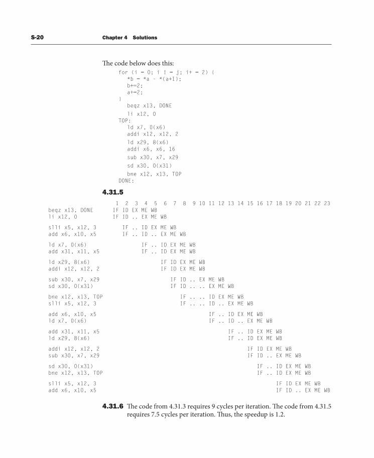
S-20 Chapter 4 Solutions
Th e code below does this: for (i = 0; i ! = j; i+ = 2) {
*b = *a - *(a+1); b+=2; a+=2;
} beqz x13, DONE
li x12, 0 TOP:
ld x7, 0(x6) addi x12, x12, 2
ld x29, 8(x6) addi x6, x6, 16
sub x30, x7, x29
sd x30, 0(x31)
bne x12, x13, TOP DONE:
4.31.5
1 2 3 4 5 6 7 8 9 10 11 12 13 14 15 16 17 18 19 20 21 22 23 beqz x13, DONE IF ID EX ME WB li x12, 0 IF ID .. EX ME WB
slli x5, x12, 3 IF .. ID EX ME WB add x6, x10, x5 IF .. ID .. EX ME WB
ld x7, 0(x6) IF .. ID EX ME WB add x31, x11, x5 IF .. ID EX ME WB
ld x29, 8(x6) IF ID EX ME WB addi x12, x12, 2 IF ID EX ME WB
sub x30, x7, x29 IF ID .. EX ME WB sd x30, 0(x31) IF ID .. .. EX ME WB
bne x12, x13, TOP IF .. .. ID EX ME WB slli x5, x12, 3 IF .. .. ID .. EX ME WB
add x6, x10, x5 IF .. ID EX ME WB ld x7, 0(x6) IF .. ID .. EX ME WB
add x31, x11, x5 IF .. ID EX ME WB ld x29, 8(x6) IF .. ID EX ME WB
addi x12, x12, 2 IF ID EX ME WB sub x30, x7, x29 IF ID .. EX ME WB
sd x30, 0(x31) IF .. ID EX ME WB bne x12, x13, TOP IF .. ID EX ME WB
slli x5, x12, 3 IF ID EX ME WB add x6, x10, x5 IF ID .. EX ME WB
4.31.6 Th e code from 4.31.3 requires 9 cycles per iteration. Th e code from 4.31.5 requires 7.5 cycles per iteration. Th us, the speedup is 1.2.
Chapter 4 Solutions S-21
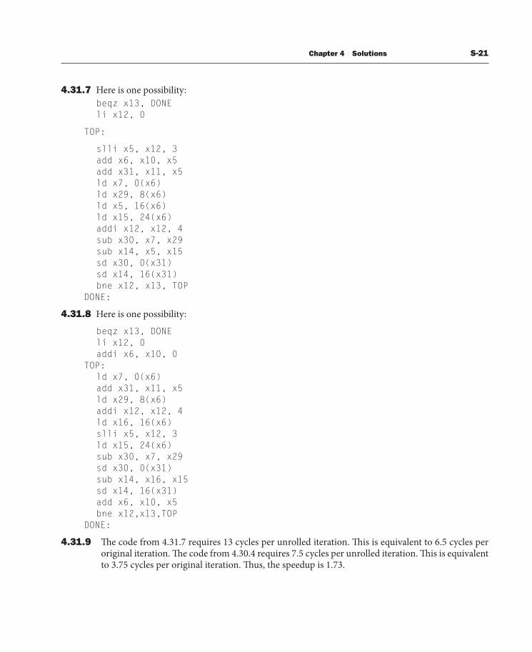
4.31.7 Here is one possibility: beqz x13, DONE li x12, 0
TOP:
slli x5, x12, 3 add x6, x10, x5 add x31, x11, x5 ld x7, 0(x6) ld x29, 8(x6) ld x5, 16(x6) ld x15, 24(x6) addi x12, x12, 4 sub x30, x7, x29 sub x14, x5, x15 sd x30, 0(x31) sd x14, 16(x31) bne x12, x13, TOP
DONE:
4.31.8 Here is one possibility:
beqz x13, DONE li x12, 0 addi x6, x10, 0
TOP: ld x7, 0(x6) add x31, x11, x5 ld x29, 8(x6) addi x12, x12, 4 ld x16, 16(x6) slli x5, x12, 3 ld x15, 24(x6) sub x30, x7, x29 sd x30, 0(x31) sub x14, x16, x15 sd x14, 16(x31) add x6, x10, x5 bne x12,x13,TOP
DONE:
4.31.9 Th e code from 4.31.7 requires 13 cycles per unrolled iteration. Th is is equivalent to 6.5 cycles per original iteration. Th e code from 4.30.4 requires 7.5 cycles per unrolled iteration. Th is is equivalent to 3.75 cycles per original iteration. Th us, the speedup is 1.73.
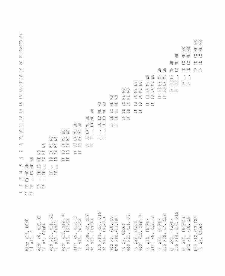
1 2 3
4 5
6 7
8 9 1
0 11
12
13 1
4 15
16
17 1
8 19
20
21 2
2 23
24
beqz x13, DONE IF ID EX
ME
WB
li x12, 0 IF ID ..
EX
ME W
B
addi x6, x10, 0 IF ..
ID
EX M
E WB
ld x7, 0(x6) IF ..
ID
.. E
X ME
WB
add x31, x11, x5
IF
.. I
D EX
ME
WB
ld x29, 8(x6)
IF
.. I
D EX
ME
WB
addi x12, x12, 4
IF
ID E
X ME
WB
ld x16, 16(x6)
IF
ID E
X ME
WB
slli x5, x12, 3
IF I
D EX
ME
WB
ld x15, 24(x6)
IF I
D EX
ME
WB
sub x30, x7, x29
IF
ID E
X ME
WB
sd x30, 0(x31)
IF
ID .
. EX
ME
WB
sub x14, x16, x15
IF .
. ID
EX
ME W
B sd x14, 16(x31)
IF .
. ID
EX
ME W
B
add x6, x10, x5
IF I
D EX
ME
WB
bne x12,x13,TOP
IF I
D EX
ME
WB
ld x7, 0(x
6)
IF
ID E
X ME
WB
add x31, x11, x5
IF
ID E
X ME
WB
ld x29, 8(x6)
IF I
D EX
ME
WB
addi x12, x12, 4
IF I
D EX
ME
WB
ld x16, 16(x6)
IF
ID E
X ME
WB
slli x5, x12, 3
IF
ID E
X ME
WB
ld x15, 24(x6)
IF I
D EX
ME
WB
sub x30, x7, x29
IF I
D EX
ME
WB
sd x30, 0(x31)
IF
ID E
X ME
WB
sub x14, x16, x15
IF
ID ..
EX M
E WB
sd x14, 16(x31)
IF .
. ID
EX
ME W
B add x6, x10, x5
IF .
. ID
EX
ME W
B
bne x12,x13,TOP
IF I
D EX
ME
WB
ld x7, 0(x6)
IF I
D EX
ME
WB
Chapter 4 Solutions S-23
4.31.10 Using the same code as in 4.31.8, the new data path provides no net improvement, because there are no stalls due to structural hazards.
4.32
4.32.1 Th e energy for the two designs is the same: I-Mem is read, two registers are read, and a register is written. We have: 140pJ + 2*70pJ + 60j = 340pJ.
4.32.2 Th e instruction memory is read for all instructions. Every instruction also results in two register reads (even if only one of those values is actually used). A load instruction results in a memory read and a register write; a store instruction results in a memory write; all other instructions result in at most a single register write. Because the sum of memory read and register write energy is larger than memory write energy, the worst-case instruction is a load instruction. For the energy spent by a load, we have: 140pJ + 2*70pJ + 60pJ + 140pJ = 480pJ.
4.32.3 Instruction memory must be read for every instruction. However, we can avoid reading registers whose values are not going to be used. To do this, we must add RegRead1 and RegRead2 control inputs to the Registers unit to enable or disable each register read. We must generate these control signals quickly to avoid lengthening the clock cycle time. With these new control signals, a load instruction results in only one register read (we still must read the register used to generate the address), so our change saves 70pJ (one register read) per load. Th is is a savings of 70/480 = 14.6%.
4.32.4 jal will benefi t, because it need not read any registers at all. I-type instructions will also benefi t because they need only read one register. If we add logic to detect x0 as a source register, then instructions such as beqz (i.e. beq x0 , …) and li ( addi xn, x0 , …) could benefi t as well.
4.32.5 Before the change, the Control unit decodes the instruction while register reads are happening. Aft er the change, the latencies of Control and Register Read cannot be overlapped. Th is increases the latency of the ID stage and could aff ect the processor’s clock cycle time if the ID stage becomes the longest-latency stage. However, the sum of the latencies for the register read (90ps) and control unit (150ps) are less than the current 250ps cycle time.
4.32.6 If memory is read in every cycle, the value is either needed (for a load instruction), or it does not get past the WB Mux (for a non-load instruction that writes to a register), or it does not get written to any register (all other instructions, including branches and stalls). Th is change does not aff ect clock cycle time because the clock cycle time must already allow enough time for memory to be read in the MEM stage. It can aff ect overall performance if the unused memory reads cause cache misses.
S-24 Chapter 4 Solutions
Th e change also aff ects energy: A memory read occurs in every cycle instead of only in cycles when a load instruction is in the MEM stage. Th is increases the energy consumption by 140pJ during 75% of the 250ps clock cycles. Th is corresponds to a consumption of approximately 0.46 Watts (not counting any energy consumed as a result of cache misses).
4.33
4.33.1 To test for a stuck-at-0 fault on a wire, we need an instruction that puts that wire to a value of 1 and has a diff erent result if the value on the wire is stuck at zero.
If the least signifi cant bit of the write register line is stuck at zero, an instruction that writes to an odd-numbered register will end up writing to the even-numbered register. To test for this (1) place a value of 10 in x1 , 35 in x2 , and 45 in x3 , then (2) execute add x3, x1, x1 . Th e value of x3 is supposed to be 20. If bit 0 of the Write Register input to the registers unit is stuck at zero, the value is written to x2 instead, which means that x2 will be 40 and x3 will remain at 45.
4.33.2 Th e test for stuck-at-zero requires an instruction that sets the signal to 1; and the test for stuck-at-1 requires an instruction that sets the signal to 0. Because the signal cannot be both 0 and 1 in the same cycle, we cannot test the same signal simultaneously for stuck-at-0 and stuck-at-1 using only one instruction.
Th e test for stuck-at-1 is analogous to the stuck-at-0 test: (1) Place a value of 10 in x1 , 35 in x2 , and 45 in x3 , then (2) execute add x2, x1, x1 . Th e value of x2 is supposed to be 20. If bit 0 of the Write Register input to the registers unit is stuck at 1, the value is written to x3 instead, which means that x3 will be 40 and x2 will remain at 35.
4.33.3 Th e CPU is still usable. Th e “simplest” solution is to re-write the compiler so that it uses odd-numbered registers only (not that writing compliers is especially simple). We could also write a “translator” that would convert machine code; however, this would be more complicated because the translator would need to detect when two “colliding” registers are used simultaneously and either (1) place one of the values in an unused register, or (2) push that value onto the stack.
4.33.4 To test for this fault, we need an instruction for which MemRead is set to 1, so it has to be ld. The instruction also needs to have branch set to 0, which is the case for ld. Finally, the instruction needs to have a different result MemRead is incorrectly set to 0. For a load, setting MemRead to 0 results in not reading memory. When this happens, the value placed in the register is “random” (whatever happened to be at
Chapter 4 Solutions S-25
the output of the memory unit). Unfortunately, this “random” value can be the same as the one already in the register, so this test is not conclusive.
4.33.5 Only R-type instructions set RegRd to 1. Most R-type instructions would fail to detect this error because reads are non-destructive—the erroneous read would simply be ignored. However, suppose we issued this instruction: add x1, x0, x0 . In this case, if MemRead were incorrectly set to 1, the data memory would attempt to read the value in memory location 0. In many operating systems, address 0 can only be accessed by a process running in protected/kernel mode. If this is the case, then this instruction would cause a segmentation fault in the presence of this error.