cavity enhanced internal photoemission effect in silicon photodiode for sub-bandgap detection
TRANSCRIPT

3266 JOURNAL OF LIGHTWAVE TECHNOLOGY, VOL. 28, NO. 22, NOVEMBER 15, 2010
Cavity Enhanced Internal Photoemission Effect inSilicon Photodiode for Sub-Bandgap Detection
Maurizio Casalino, Giuseppe Coppola, Member, IEEE, Mariano Gioffrè, Mario Iodice, Luigi Moretti,Ivo Rendina, and Luigi Sirleto
Abstract—In this paper, a new approach for the near infraredsub-bandgap detection in Si-based devices is investigated. In par-ticular, the design, the realization and the characterization of aback illuminated silicon resonant cavity enhanced Schottky pho-todetectors, working at 1.55 m, are reported.
The photodetectors are constituted by Fabry–Perot microcavityincorporating a Schottky diode. The working principle is based onthe internal photoemission effect enhanced by cavity effect. Perfor-mances devices in terms of responsivity, free spectral range, finesseand estimated bandwidth are reported.
Index Terms—Fabry-Perot, internal photoemission, photodetec-tors, resonant cavity enhanced, silicon.
I. INTRODUCTION
S ILICON-based photodetectors (PDs) working at 1550 nmare of great interest, not only for fiber communications,
but also for inter- and intra-chip optical interconnects. One ofthe reasons is that a direct monolithic integration of photode-tectors in a chip would be possible, which is the best optionin order to integrate optical receivers with electronics. Unfortu-nately, because of the inter-band transition, Silicon (Si) exhibitsan unavoidable cut-off wavelength at about 1.1 m [1]. There-fore, in order to realize photodetectors working at 1.55 m, wehave two possible options. The first is to use a semiconductoras Germanium (Ge) which is sensitive at that wavelength. Gephotodetectors monolithically integrated on silicon have shownimpressive advances during the last years [2], [3]. However, theaggressive substrate cleaning processes and thermal mismatchbetween Ge and Si hinder a seamless integration of Ge-PDs withthe standard Si integrated circuit realization. For these reasons,unfortunately, their fabrication and related technology are muchmore expensive than those most diffused and advanced, whichare based on silicon [4], [5].
The second option is a sub-bandgap all-Silicon photode-tector. To this aim, in this paper the exploitation of the internalphotoemission effect in a metal-semiconductor Schottky bar-rier [6] is exploited. Silicon infrared photodiodes based on
Manuscript received May 28, 2010; revised July 14, 2010, September 14,2010; accepted September 17, 2010. Date of publication September 27, 2010;date of current version November 19, 2010.
M. Casalino, G. Coppola, M. Gioffrè, M. Iodice, I. Rendina, and L. Sirleto arewith the Istituto per la Microelettronica e Microsistemi sez. Napoli—ConsiglioNazionale delle Ricerche (IMM-CNR), Napoli 80131, Italy (e-mail: [email protected]).
L. Moretti is with the Dipartimento di Matematica—Seconda Universita'degli Studi di Napoli , 81100 Caserta, Italy.
Color versions of one or more of the figures in this paper are available onlineat http://ieeexplore.ieee.org.
Digital Object Identifier 10.1109/JLT.2010.2081346
the internal photoemission effect are usually employed in theinfrared imaging systems [7]. The main advantages of thesedevices resides in their extremely large bandwidth and simplefabrication process, but unfortunately, the quantum efficiencyof these devices is very low [7].
In this paper, the design, the realization and the characteriza-tion of back illuminated silicon resonant cavity enhanced (RCE)Schottky photodetectors, working at 1.55 m, are reported. Wenote that the resonant cavity structure is not a new concept inphotodetector design [8]–[10], while it is quite new to incor-porate into RCE structure a photodetector based on internalphotoemission effect. Finally, we point out that our structureis different from the classical RCE Schottky PDs, in which theSchottky contact is only an electric contact and not the activelayer. In our device, the metal layer works as top contact, as ac-tive (absorbing) layer and as mirror. This is the crucial point andthe novelty of our device.
A theoretical and numerical analysis of these structures wasprovided by the same authors in a previous work [11]. In partic-ular, the quantum efficiency, bandwidth and dark current den-sity of top illuminated RCE photodetectors were calculated asa function of bias voltage. However, regarding top-illuminatedstructures, the crucial point is the realization of a semitrans-parent thin metal film. The precise control of metal thicknessin the 0–50 nm range and an acceptably low defect concentra-tions are not trivial tasks. Therefore, in our previous papers, thetheoretical analysis of a back illuminated RCE photodetectorworking at 1.55 micron [12] and its fabrication and characteriza-tion [13] were reported. In [13] a comparison between a Cu/p-SiSchottky diode and a Cu/p-Si Schottky diode fed on a high re-flectivity Bragg mirror, was reported and an improvement in ex-ternal responsivity at 1.55 m was experimentally demonstratedfor the first time.
In this paper, in order to go towards higher integration den-sity and to improve the device performances, we carry out thescaling down of the device reported in [13]. We experimentallydemonstrate that reducing the device size, a further improve-ment in external responsivity can be obtained. Finally parallelresistance and capacitance photodiode, as a function of the re-verse bias, are measured in order to estimate the bandwidthdevice.
II. DEVICE DESIGN
The sketch of the device is shown in Fig. 1. The resonantcavity is a vertical-to-the-surface Fabry–Perot structure. It isformed by a buried reflector, a top mirror interface and, in themiddle, a silicon cavity. The buried reflector is a high reflec-tivity Bragg mirror, realized by 5 periods of alternating layers
0733-8724/$26.00 © 2010 IEEE
CASALINO et al.: CAVITY ENHANCED INTERNAL PHOTOEMISSION EFFECT 3267
Fig. 1. Schematic cross section of the proposed RCE Schottky photodetector.
of amorphous hydrogenated silicon (a-Si:H) and silicon nitride(Si N ). A Schottky metal layer, working also as top reflectorof the resonant cavity, is deposited above the silicon layer.
The RCE-PD is based on the internal photoemission effect ina Schottky junction metal-Si, back illuminated and operating at1.55 m. Internal photoemission is the optical excitation of elec-trons in the Schottky metal to energy above the Schottky barrierand then transport of these electrons into the semiconductor. De-pending on the height of the metal semiconductor barrier, thecut-off wavelength of Schottky photodiodes can be changed. Inparticular, the maximum detectable wavelength is given by
nm (1)
where is the Schottky barrier heigh. In order to obtain asuitable responsivity at the wavelength of 1.55 m, and moregenerally in the optical band, Copper has been chosenas metal. Even if this metal doesn’t allow a full silicon tech-nology compatibility, due to its rapid diffusion into the silicon,in this work has been used to prove the feasibility of an in-ternal photoemission based all-silicon photodetector. However,for future CMOS-compatible applications, it is mandatory to re-place the copper layer with new materials, such as nickel silicidelayer [14].
The responsivity of the RCE-PD is given by (2) [11]
nm nm(2)
where is the quantum efficiency, is the total optical ab-sorbance of the metal [11], is the fraction of absorbed pho-tons which produce photoelectrons with appropriate energy tocontribute to the photocurrent [15], is the total accumulatedprobability that one of these photoexcited electrons will over-come the Schottky barrier after scattering with cold electrons
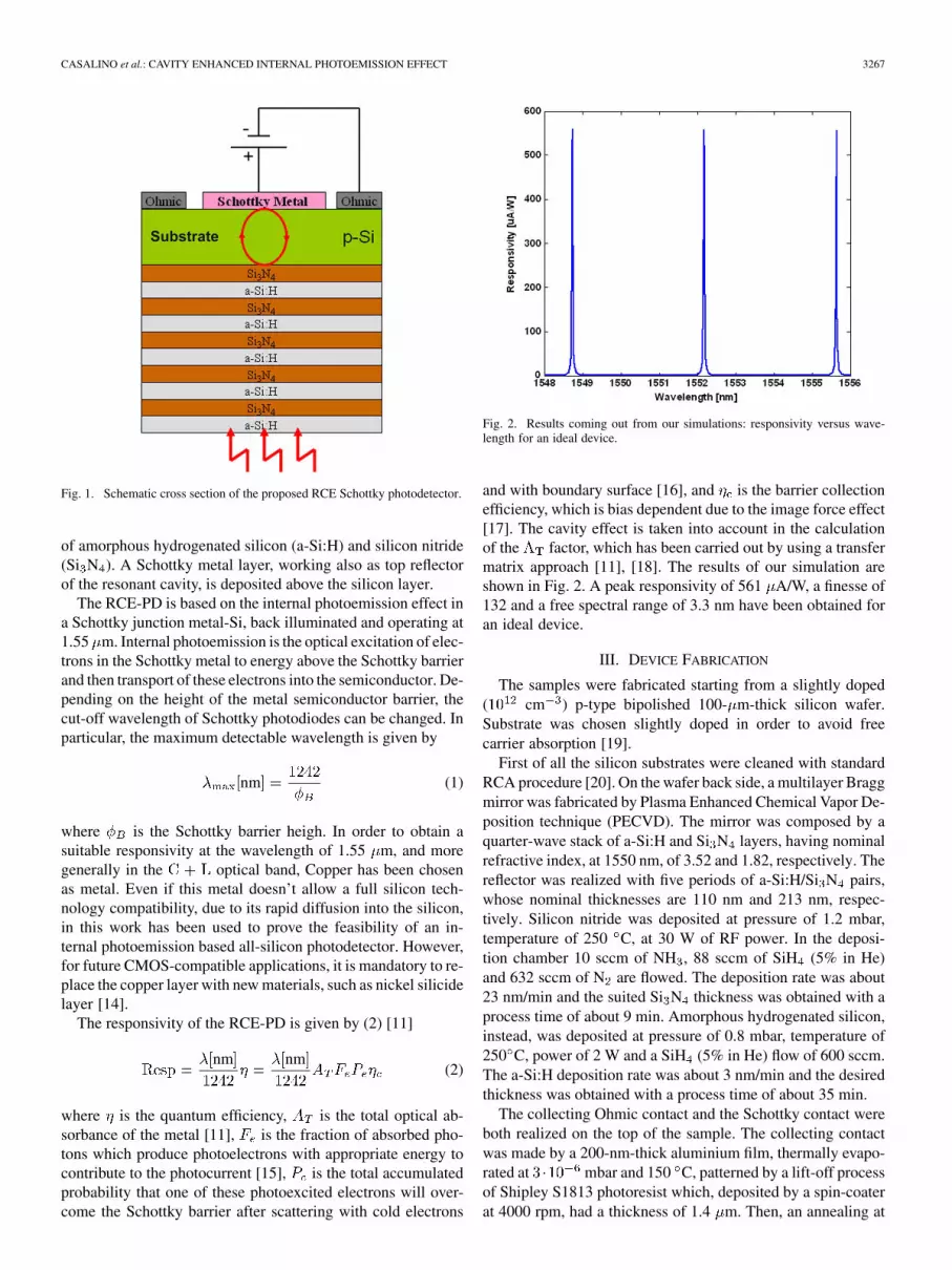
Fig. 2. Results coming out from our simulations: responsivity versus wave-length for an ideal device.
and with boundary surface [16], and is the barrier collectionefficiency, which is bias dependent due to the image force effect[17]. The cavity effect is taken into account in the calculationof the factor, which has been carried out by using a transfermatrix approach [11], [18]. The results of our simulation areshown in Fig. 2. A peak responsivity of 561 A/W, a finesse of132 and a free spectral range of 3.3 nm have been obtained foran ideal device.
III. DEVICE FABRICATION
The samples were fabricated starting from a slightly doped( cm ) p-type bipolished 100- m-thick silicon wafer.Substrate was chosen slightly doped in order to avoid freecarrier absorption [19].
First of all the silicon substrates were cleaned with standardRCA procedure [20]. On the wafer back side, a multilayer Braggmirror was fabricated by Plasma Enhanced Chemical Vapor De-position technique (PECVD). The mirror was composed by aquarter-wave stack of a-Si:H and Si N layers, having nominalrefractive index, at 1550 nm, of 3.52 and 1.82, respectively. Thereflector was realized with five periods of a-Si:H/Si N pairs,whose nominal thicknesses are 110 nm and 213 nm, respec-tively. Silicon nitride was deposited at pressure of 1.2 mbar,temperature of 250 C, at 30 W of RF power. In the deposi-tion chamber 10 sccm of NH , 88 sccm of SiH (5% in He)and 632 sccm of N are flowed. The deposition rate was about23 nm/min and the suited Si N thickness was obtained with aprocess time of about 9 min. Amorphous hydrogenated silicon,instead, was deposited at pressure of 0.8 mbar, temperature of250 C, power of 2 W and a SiH (5% in He) flow of 600 sccm.The a-Si:H deposition rate was about 3 nm/min and the desiredthickness was obtained with a process time of about 35 min.
The collecting Ohmic contact and the Schottky contact wereboth realized on the top of the sample. The collecting contactwas made by a 200-nm-thick aluminium film, thermally evapo-rated at mbar and 150 C, patterned by a lift-off processof Shipley S1813 photoresist which, deposited by a spin-coaterat 4000 rpm, had a thickness of 1.4 m. Then, an annealing at

3268 JOURNAL OF LIGHTWAVE TECHNOLOGY, VOL. 28, NO. 22, NOVEMBER 15, 2010
Fig. 3. Top view of the proposed fabricated device. AA transverse section issketched in Fig. 1.
Fig. 4. SEM image of the realized Bragg mirror formed by 5 periods ofa-Si:H/Si N pairs.
475 C in nitrogen for 30 min, in order to get a not-rectifyingbehaviour, was carried out [21].
Finally, the Schottky contact was fabricated. Both sides of thewafer were covered by Shipley S1813 photoresist and the frontside was exposed and developed for the Cu contact realization.The samples were dipped in a mixture of hydrofluoric acid (HF)and water (2% of HF) for 1 min in order to remove the residualnative oxide, rinsed in deionized water and blown by nitrogen.Then copper was thermally evaporated and patterned by lift-off, so obtaining a metal film thickness of 200 nm, thicker thanoptical field penetration depth. The collecting contact and theSchottky contact are shaped into concentring ring (inner rardius44 m and external radius 48 m) and disk (with a radius of 40
m), respectivily. In Fig. 3 a top view of the photodetector isreported.
IV. BRAGG MIRROR CHARACTERIZATION
As far as the realization of our device is concerned, the crucialpoint is the Bragg mirror. Therefore, a number of characteriza-tion were performed in order to check its optical and structuralproperties.
First of all, a SEM characterization was performed. Theimage of the realized Bragg mirror formed by 5 periods ofSi N /a-Si:H pairs is reported in Fig. 4.
After that in order to perform the PECVD process utilized forthe Bragg mirror fabrication and to monitor thicknesses and di-electric characteristics of the deposited thin films, an accurate
Fig. 5. Refractive index of a-Si:H (up) and Si N (down) calculated from theTauc-Lorentz model.
TABLE IVALUE OF THICKNESS AND REFRACTIVE INDEX AS CALCULATED
Fig. 6. Measured and calculated reflectance of the Bragg mirror from 600 to1600 nm.
analysis was carried out by means of Spectroscopic Ellipsom-etry (SE) [22], [23]. Spectroscopic ellipsometric data were ac-quired by a Jobin Yvon UVISEL-NIR phase modulated spec-troscopic ellipsometer apparatus, at 70 angle of incidence, op-erating from 280 to 1600 nm.
The optical properties of a-Si:H and Si N , i. e. the com-plex refractive index dispersion spectra, were calculated usingthe Tauc-Lorentz dispersion model [24]–[26]. The results con-cerning refractive index and extinction coefficient dispersioncurves of a-Si:H and Si N , are reported in Fig. 5.
The mean value , the standard deviation for botha-Si:H and Si N films thickness and the refractive indexes
value at nm are summarized in Table I.Finally, reflectivity measurements into the range 600–1600
nm were performed. As you can see, in Fig. 6 a reflectivity of

CASALINO et al.: CAVITY ENHANCED INTERNAL PHOTOEMISSION EFFECT 3269
Fig. 7. J-V characteristic of the realized Cu/p-Si Schottky diode. The insetshows diodes dark current.
about 0.99 in a 200-nm-wide range spanning from 1400 to 1600nm was obtained. The Bragg mirror theoretical model is com-posed by five distinct pairs of a-Si:H/Si N layers, depositedon single crystal silicon substrate, and by a superficial rough-ness, modelled by a Bruggeman effective medium approxima-tion (EMA) [27], consisting of 50% of air and 50% of a-Si. Thefitting procedure between the experimental data and the theoret-ical model was executed using the Levenberg-Marquardt algo-rithm and returned a fit goodness factor . The compar-ison between simulated and measured Bragg mirror reflectivityfor normal light incident into the range 600–1600 nm is also re-ported. Of course, ellipsometric data were used to accommodatemore accurate simulations.
V. DEVICE CHARACTERIZATION
A. Electrical Characterization
Typical density current-voltage (J-V) curve of Cu/p-Sidiodes, obtained by a parameter analyzer (Hewlett Packard4145B), are depicted in Fig. 7. The Schottky barrier height(SBH) is deduced fitting the experimental J-V characteristicin the forward bias region by the following equation of theSchottky diode (3) [17]
(3)
where Rs is the series resistance, the potential barrier, theideality factor, T the absolute temperature and is the thermalvoltage. The calculated SBH and series resistance are 0.55 eVand 6.9 k , respectively. The high series resistance and darkcurrent are due to a slight rectifying effect of the aluminiumelectrode realized on top of lightly doped p-type silicon. How-ever, ohmic contacts can easily be optimized in future devices byan heavy p-doping implantation into the collection pad region.
B. Optical Characterization
The experimental setup for external responsivity measure-ments is shown in Fig. 8. The laser beam emitted by a wave-length tunable laser, is split by a Y fiber junction. One branch is
Fig. 8. Experimental setup for external responsivity measurements.
Fig. 9. Measured external responsivity versus wavelength for the proposed andfabricated Cu/p-Si photodetector at ���� mV.
used to monitor the optical power, while the other one is colli-mated, chopped and focused onto the device by a long workingdistance 50 microscope objective providing a beam diameterof about 5 m.
The photocurrent produced by our device is measured by alock-in amplifier. A trans-impedance amplifier is employed toprovide a reverse bias voltage to the photodetector, and at thesame time for reducing the dark current. The dark current can-cellation circuit realised by using a trans-impedance amplifierhas a limited bandwidth, however it is adequate for our scope,that is DC or quasi-static measurements [28].
Measurements into the range of 1545–1556 nm (step of0.001 nm) at 100 mV of reverse bias applied, were carried out(Fig. 9). We observe three distinct peaks. The measured freespectral range of 3.3 nm agrees the value calculated by theformula: [8], where is the central wave-length at the considered range (1550nm), n is the silicon cavityrefractive index (3.48 at 1550 nm [29]) and L is the siliconcavity thickness (100 m). A peak external responsivity and anexperimental finesse of about of 8 A/W and 33, respectively,are obtained.
We note that while the experimental and numerical free spec-tral range agree, as finesse and peak responsivity are concerned,experimental and numerical values show a discrepancy.
In our opinion, such a discrepancy can be due to the cavitylosses, which are not taken into account in our simulations. In

3270 JOURNAL OF LIGHTWAVE TECHNOLOGY, VOL. 28, NO. 22, NOVEMBER 15, 2010
fact, it is well known that if we assume a Fabry–Perot inter-ferometer (FPI) having ideal plane-parallel plates, the finesse isdetermined only by the reflectivity R of the mirrors. However,in practice deviations of the surfaces from an ideal plane, slightinclinations of the two surfaces and surface irregularities, causeimperfect superposition of the interfering waves. For this reasona broadening and lowering of the transmission peak, resultantin a decreasing in finesse and responsivity of the device, can beexpected [30]. Moreover, both the interstitials defects inducedby copper diffusion and the not perfect Ohmic contact hamperthe carriers collection [31], furthermore lowering the measuredresponsivity.
In our previous paper [13] a macroscopic device (radius ofabout 2 mm) was considered and peak external responsivityvalue of 4.3 A/W and a finesse value of 4.7 were reported. Inthis paper a microscopic device (radius of 40 m) is investigatedand an increasing in finesse and responsivity has been obtained.In our opinion, reducing the device dimensions, the imperfec-tion and hence of losses are reduced, too. Therefore, improvedresponsivity and finesse were expected.
C. Photodetector Bandwidth
It is well known that the 3 dB bandwidth is determined by thecarrier transit time and RC delay of the device [32]
dB (5)
The transit time limited bandwidth is given by
(6)
where is the effective Si carrier saturation velocity (10 cms and is the depletion width. For a calculated depletionwidth of 2.74 m at mV, a GHz can beestimated.
Moving our attention on the RC constant contribution, themodel for small signal shown as inset of Fig. 10 has beenadopted [28].
Starting from it, the RC limited bandwidth is given by
(7)
In the sketch, the photodetector schematized as a current gen-erator , the resistance and capacitance associ-ated to the junction, the series resistance and the load re-sistance , are reported.
has been evaluated from the inverse derivative of thecurrent-voltage characteristic plotted as inset in Fig. 7, re-sulting greater than 60 k at any reverse bias and 0.2 Mat mV while device capacitance has been measuredby a LCZ meter (Keithley-3322). The measured capacitanceis smaller than 10 pF at any reverse bias and about 5 pF at
mV (Fig. 10).On the other hand, k , extracted from the I–V
characteristic (see Fig. 7), results both much greater than loadresistance (typically 50 and much smaller than parallel re-sistance .
Fig. 10. Measured junction capacitance versus reverse bias. The inset showsthe equivalent circuit for small-signal analysis.
Hence the device dB frequency, becomes
dB (8)
and estimated device bandwidth is limited to megahertz range.It is worth noting that if collection contact were perfectly
Ohmic, the series resistance would be a fraction of ohmand would be coincident with . In this case the dBachieves the GHz range. Moreover, by reducing photodetectorarea (hence its capacitance) a rather improvement in dBbandwidth could be obtained. Unfortunately, due to the absenceof a heavily doped region under the contact, of our realizeddevice is about four orders of magnitude higher than a typical se-ries resistance and this considerably hampers the photodetectorresponse.
Finally, the SBH deduced by fitting the experimental C–Vcharacteristic is 0.55 eV. The same value has been obtained byfitting the experimental I–V characteristic (Fig. 7); the agree-ment demonstrates that SBH is not determined by presence ofdefects at interface [33].
VI. CONCLUSION
In this paper, silicon resonant cavity enhanced photodetectorsbased on the internal photoemission effect have been designed,fabricated and characterized.
The preliminary device exhibits a responsivity of about 8A/W at around 1550 nm and the capacitance measurements
(pF) encourage pursuing increased bandwidth toward severalGbit/s operation.
On the other hand, even if responsitvity could be improved byoptimizing a number of parameters, first of all the Ohmic con-tacts quality, at that time, its value could be suitable for powermonitoring applications.
By comparing experimental results of this paper with the onesreported in our previous paper [13], we experimentally demon-strate that an improvement in responsivity can be obtained in-creasing the cavity finesse. Hence, proposed photodetector re-

CASALINO et al.: CAVITY ENHANCED INTERNAL PHOTOEMISSION EFFECT 3271
sults very promising for integration in more complex micro-cavity having very high finesse (for example disk or ring res-onator) which could allow the integration on silicon waveguideand a further enhancement in responsivity. However, in order toobtain a real silicon technology compatible device, it is manda-tory to replace the copper layer with new materials which couldallow a further increasing in responsivity, too.
REFERENCES
[1] H. Zimmermann, Silicon Photo-Receivers in Topics Appl. Physics.New York: Springer, 2004.
[2] L. Vivien, M. Rouvière, J. M. Fédéli, D. Marris-Morini, J. F. Damlen-court, J. Mangeney, P. Crozat, L. El Melhaoui, E. Cassan, X. Le Roux,D. Pascal, and S. Laval, “High speed and high responsivity germa-nium photodetector integrated in a silicon-on-insulator microwaveg-uide,” Opt. Exp., vol. 15, p. 9843, 2007.
[3] T. Yin, R. Cohen, M. M. Morse, G. Sarid, Y. Chetrit, D. Rubin, and M.J. Paniccia, “31 GHz Ge n-i-p waveguide photodetectors on silicon-on-insulator substrate,” Opt. Exp., vol. 15, p. 13965, 2007.
[4] G. Masini, L. Colace, and G. Assanto, “2.5 Gbit/s polycrystallinegermanium-on-silicon photodetector operating from 1.3 to 1.55 �m,”Appl. Phys. Lett, vol. 82, p. 2524, 2003.
[5] L. Colace, P. Ferrara, G. Assanto, D. Fulgoni, and L. Nash, “Lowdark-current germanium-on-insulator near-infrared detectors,” IEEEPhoton. Technol. Lett., vol. 19, no. 22, pp. 1813–1815, Nov. 2007.
[6] B. Aslan and R. Turan, “On internal photoemission spectrum ofPt/Si/p-Si infrared detectors,” Infrared Physics & Technology, vol. 43,p. 85, 2002.
[7] W. F. Kosonocky, F. V. Shallcross, and T. S. Villani, “160� 244 ele-ment PtSi schottky-barrier IR-CCD image sensor,” IEEE Trans. Elec-tron Dev., vol. ED-32, no. 8, p. 1564, Aug. 1985.
[8] M. S. Unlu and S. Strite, “Resonant cavity enhanced (RCE) photonicdevices,” Appl. Phys. Rev., vol. 78, p. 607, 1995.
[9] M. K. Emsley, O. I. Dosunmu, and M. S. Unlu, “High-speed resonant-cavity-enhanced silicon photodetectors on reflecting silicon-on-insu-lator substrates,” IEEE Photon. Technol. Lett., vol. 14, no. 4, p. 519,Nov. 2002.
[10] O. I. Dosunmu, D. D. Cannon, M. K. Emsley, L. C. Kimerling, and M.S. Unlu, “High-speed resonant cavity enhanced Ge photodetectors onreflecting Si substrates for 1550-nm operation,” IEEE Photon. Technol.Lett., vol. 17, no. 1, p. 175, Jan. 2005.
[11] M. Casalino, L. Sirleto, L. Moretti, and I. Rendina, “A novel silicon res-onant cavity enhanced photodetectors working at 1.55 micron,” Semi-cond. Sci. Technol., vol. 23, p. 075001, 2008.
[12] M. Casalino, L. Sirleto, L. Moretti, M. Gioffrè, G. Coppola, M. Iodice,and I. Rendina, “Back-illuminated silicon resonant cavity-enhancedphotodetector at 1550 nm,” Physica E, vol. 41, pp. 1097–1101, 2009.
[13] M. Casalino, L. Sirleto, L. Moretti, M. Gioffrè, G. Coppola, and I. Ren-dina, “Silicon resonant cavity enhanced photodetector based on the in-ternal photoemission effect at 1.55 micron: Fabrication and character-ization,” Appl. Phys. Lett., vol. 92, p. 251104, 2008.
[14] S. Zhu, G. Q. Lo, and D. L. Kwong, “Low-cost and high-speed SOIwaveguide-based silicide schottky-barrier MSM photodetectors forbroadband optical communications,” IEEE Photon.Technol. Lett., vol.20, no. 16, pp. 1396–1398, Aug. 2008.
[15] R. H. Fowler, “The analysis of photoelectric sensitivity curves for cleanmetals at various temperatures,” Phys. Rev., vol. 38, p. 45, 1931.
[16] V. E. Vickers, “Model of schottky barrier hot-electron-mode photode-tection,” Appl. Opt., vol. 10, p. 2190, 1971.
[17] S. M. Sze, Physics of Semiconductor Devices. New York: Wiley,1981.
[18] M. A. Muriel and A. Carballar, “Internal field distributions in fiberbragg gratings,” IEEE Photon.Technol. Lett., vol. 9, no. 7, p. 955, Jul.1997.
[19] D. K. Schroder, R. N. Thomas, and J. C. Swarts, “Free carrier absorp-tion in silicon,” IEEE Trans Electron. Devices, vol. ED-25, no. 1, pp.254–261, Jul. 1978.
[20] W. Kern and D. A. Puotinen, “Cleaning solutions based on hydrogenperoxide for use in silicon semiconductor technology,” RCA Rev., vol.31, pp. 187–206, 1970.
[21] H. C. Card, “Aluminum-silicon schottky barriers and ohmic contactsin integrated circuits,” IEEE Trans Electron. Devices, vol. ED-23, no.6, pp. 538–544, Jun. 1976.
[22] K. Vedam, “Spectroscopic ellipsometry: A historical overview,” ThinSolid Films, vol. 313–314, pp. 764–774, 1998.
[23] G. E. Jellison Jr, “The calculation of thin film parameters from spectro-scopic ellipsometry data,” Thin Solid Films, vol. 290–291, pp. 40–45,1996.
[24] G. E. Jellison, Jr. and F. A. Modine, “Parameterization of the opticalfunctions of amorphous materials in the interband region,” Appl. Phys.Lett., vol. 69, pp. 371–372, 1996.
[25] G. E. Jellison, Jr., F. A. Modine, P. Doshi, and A. Rohatgi, “Spectro-scopic ellipsometry characterization of thin-film silicon nitride,” ThinSolid Films, vol. 313–314, pp. 193–197, 1998.
[26] P. Doshi, G. E. Jellison Jr., and A. Rohatgi, “Characterization and opti-mization of absorbing plasma-enhanced chemical vapor deposited an-tireflection coatings for silicon photovoltaics,” Appl. Opt., vol. 36, pp.7826–7837, 1997.
[27] D. E. Aspnes and J. B. Theeten, “Investigation of effective-mediummodels of microscope surface roughness by spectroscopic ellipsom-etry,” Phys. Rev. B, vol. 20, pp. 3292–3301, 1979.
[28] S. Donati, Photodetectors: Devices, Circuits, and Applications. En-glewood Cliffs, NJ: Prentice Hall, 1999.
[29] E. D. Palik, Handbook of Optical Constants of Solids. San Diego,CA: Academic, 1985.
[30] W. Demtroder, Laser Spectroscopy Vol 1 Basic Principles. Berlin:Springer, 2008, ch. 4.
[31] H. Norde, “A modified forward I–V plot for Schottky diodes with highseries resistance,” J. Appl. Phys., vol. 50, pp. 5052–5053, 1979.
[32] J. Liu, J. Michel, W. Giziewicz, D. Pan, K. Wada, D. D. Cannon, S.Jongthammanurak, D. T. Danielson, and L. C. Kimerling, “High-per-formance, tensile strained Ge p-i-n photodetectors on a Si platform,”Appl. Phys. Lett., vol. 87, p. 103501, 2005.
[33] E. H. Rhoderick and R. H. Williams, Metal-Semiconductor Con-tacts. Oxford, U.K.: Oxford Univ. Press, 1978.
Maurizio Casalino was born in Napoli, Italy, in 1974. He received the Elec-tronic Engineering degree (cum laude) in 2003 from the University Federico II,Napoli, Italy, his thesis work has concerned the study of the electro-thermal ef-fects of integrated poles by developing and optimizing a software dedicated tocarry out electro-thermal simulations of power bipolar devices. He received thePh.D. degree in electronics engineering in 2008 from the University “Mediter-ranea,” Reggio Calabria, Italy, working at the design, fabrication and character-ization of silicon photodetectors working at 1.55 micron.
Currently he is researcher at IMM-CNR, Department of Napoli, and his re-search interests include design, fabrication, characterization and modelling ofsemiconductor optoelectronic and electronic devices. He has an extensive expe-rience in the field of the technologies for the manufacture of silicon semicon-ductor devices.
Giuseppe Coppola (M’06) received the M.Sc. degree in electronic engineeringand the Ph.D. degree in electronics and computer science in 1997 and 2001,respectively, both from the University of Napoli “Federico II,” Italy.
In 2001, he spent six months as Visiting Scientist at Delft Institute of Mi-croelectronics and Submicron Technologies, Technical University of Delft, TheNetherlands, working on the design and realization of an optoelectronic modu-lator. Since 2004, he has been a contract professor at the University of Calabria,for a course on the silicon-based microsystems. He is now pursuing his interestsin the design and fabrication of optoelectronic devices, and their characteriza-tion with contactless interferometric techniques, such as the digital holography.
Mariano Gioffrè was born in Reggio Calabria, Italy, in 1972. He graduated inelectronic engineering at the University “Mediterranea” of Reggio Calabria in2003 with a thesis on “the deposition by sputtering and characterization of a-Sithin films.” He received the Ph.D. degree in electronic engineering in 2006 fromthe Faculty of Engineering of the University of Reggio Calabria with a workconcerning the “fabrication and characterization o(e based rib waveguide”.
In December 2006 he obtained a fellowship at the Institute of Microelec-tronic and Microsystems of National Council of Research (IMM-CNR) and,from November 2008, he work as research technician, temporary position. Hisresearch activity concern the deposition and characterization of thin films ob-tained by different technologies, i.e., sputtering, e-beam evaporation, PECVD,etc. for optoelectronics applications. He has a remarkable experience in the basictechnologies for microelectronic application like lithography, thermal oxidationof silicon, wet and dry etching.

3272 JOURNAL OF LIGHTWAVE TECHNOLOGY, VOL. 28, NO. 22, NOVEMBER 15, 2010
Mario Iodice received the M.Sc. and Ph.D. degrees in electronic engineering atthe University of Napoli “Federico II,” Italy.
From 1992 to 1994 he was a scholarship holder at the IRECE-CNR, where hewas involved in integrated optics and optoelectronics and on laser characteriza-tion of electro-optic materials. From 1993 to 1994 he was a Visiting Researcherat DIMES (TUDelft), where he worked on microelectronics technologies andon thermal sensors design. From 1995 to 1997 he was with the Department ofElectronic Engineering at the University of Napoli “Federico II,” working onmodeling and design of silicon electro-optic modulator. During 1996 he vis-ited the Department of Electrical Engineering at Princeton University, where heworked on thermal analysis on flat panel displays. At the present time he is asenior researcher at IMM-CNR, where he works on integrated optical circuitand devices and optical sensors. He also taught Electronics at the University ofReggio Calabria, since 1997 until 2001 and Sensors at the University of Cal-abria in 2002. He is the responsible of the Clean Room at IMM-CNR. He isauthor of more than 150 papers published on international journals and confer-ence proceedings.
Luigi Moretti received the Laurea degree in physics from the University “Fed-erico II,” Naples, Italy, in May of 1999, and pursued his research activity on sil-icon optoelectronic devices and materials characterization. In 2003, he receivedthe Ph.D. in electronic engineering with a thesis entitled “Fabrication and Char-acterization of Silicon Optical Microcavities with IC Technologies Compatible”from the Faculty of Engineering of the University of Cosenza, Italy, under thesupervision of Prof. G. Cocorullo.
He carried out experimental works on porous silicon sensors at the NaplesUnit of the Institute of Microelectronic and Microsystems of National ResearchCouncil (IMM-CNR). He is currently a researcher at the Second University ofNaples. His main research interests are in the fields of aperiodic photonic crys-tals and advanced optoelectronics devices. He is the author or coauthor of about35 published articles in international journals and 20 in international conferenceproceedings.
Ivo Rendina was born in Naples, Italy, in 1960.He is a research director of the Italian National Council of Research (CNR),
where he is now Head of the Department of Naples of the Institute for Mi-croelectronics and Microsystems. He was previously Director of the Institutefor Electromagnetism and Electronic Components of the CNR. Since 1995 heteaches Electronics and Optoelectronics at the Electronic Engineering Depart-ment of the University of Calabria (Italy). In 1997, he was a visiting scientistat the University of California, Los Angeles.He has authored and co-authoredmore than 250 journal and conference papers in the field of silicon photonics,optical microsensors and microsystems.
Dr. Rendina is Vice-President of the Societá Italiana di Ottica e Fotonica(SIOF), Italian branch of the European Optical Society (EOS), fellow of EOS,chair of the “Advisory Council for Aeronautic Research in Europe (ACARE)”,chair and organizer of several international conferences, such as the 1st, 2nd and3rd EOS Topical Meetings on Optical MicroSystems, the EOS Annual Meetingin 2008, the XII Sensors and Microsystems Conference in 2007. He has servedas scientific and technical committee member of many international conferencesorganized by EOS, SPIE, OSA, and IEEE in the field of optics and photonics,and guest editor of international scientific journals.
Luigi Sirleto received both the degree in physics (hons) and Ph.D. degree inelectronic engineering from the University of Napoli, Italy.
In 1993, he joined the Nonlinear Optics group of Naples University PhysicsDepartment. In 1995, he joined the Photonics Department of Research Instituteon Electromagnetic Wave of the National Research Council (CNR), Florence,Italy. In 1998 he joined the Optoelectronic Group of Naples University Elec-tronic Department. Since March 2001 he has been a researcher at Institute ofMicroelectronics and Microsystems of the National Research Council (CNR).In september 2001, joining the Lightwave Devices Group, he spent 2 months, asvisiting scientist, at MESA+, Institute of Nanotechnology, University of Twente,The Netherlands. From July 2003 until March 2004, joining Photonics Labora-tory he spent 9 months, as visiting scientist, at UCLA (University of California,Los Angeles)-Electrical Engineering Department. Since september 2006 he ledthe activities of Nonlinear Optics Laboratory at IMM/CNR unit of Naples. Hehas published more than 100 scientific papers in english language includingjournals and conference proceedings. His scientific interests concerns NonlinearOptics and Nanophotonics.
Dr. Sirleto is a member of SIOF (Italian Society of Optics and Photonics)board. He is a EOS (European Optical Society) member and a SPIE member,too.