bose condensation and lasing in optical microstructures
TRANSCRIPT
arX
iv:c
ond-
mat
/020
4307
v1 1
4 A
pr 2
002 Bose Condensation and Lasing
in Optical Microstructures
Part 2
Marzena Hanna Szymanska
Trinity College
University of Cambridge
Dissertation submitted for the degree
of Doctor of Philosophy at the
University of Cambridge
October 2001
i

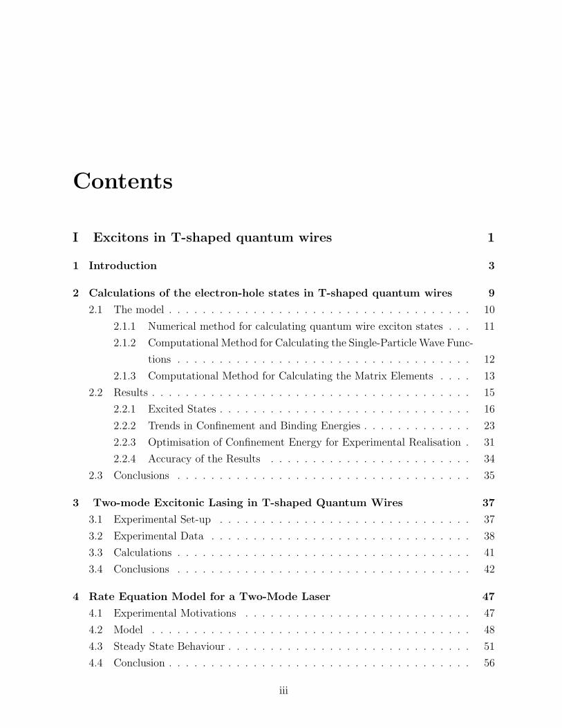
Contents
I Excitons in T-shaped quantum wires 1
1 Introduction 3
2 Calculations of the electron-hole states in T-shaped quantum wires 9
2.1 The model . . . . . . . . . . . . . . . . . . . . . . . . . . . . . . . . . . . . 10
2.1.1 Numerical method for calculating quantum wire exciton states . . . 11
2.1.2 Computational Method for Calculating the Single-Particle Wave Func-
tions . . . . . . . . . . . . . . . . . . . . . . . . . . . . . . . . . . . 12
2.1.3 Computational Method for Calculating the Matrix Elements . . . . 13
2.2 Results . . . . . . . . . . . . . . . . . . . . . . . . . . . . . . . . . . . . . . 15
2.2.1 Excited States . . . . . . . . . . . . . . . . . . . . . . . . . . . . . . 16
2.2.2 Trends in Confinement and Binding Energies . . . . . . . . . . . . . 23
2.2.3 Optimisation of Confinement Energy for Experimental Realisation . 31
2.2.4 Accuracy of the Results . . . . . . . . . . . . . . . . . . . . . . . . 34
2.3 Conclusions . . . . . . . . . . . . . . . . . . . . . . . . . . . . . . . . . . . 35
3 Two-mode Excitonic Lasing in T-shaped Quantum Wires 37
3.1 Experimental Set-up . . . . . . . . . . . . . . . . . . . . . . . . . . . . . . 37
3.2 Experimental Data . . . . . . . . . . . . . . . . . . . . . . . . . . . . . . . 38
3.3 Calculations . . . . . . . . . . . . . . . . . . . . . . . . . . . . . . . . . . . 41
3.4 Conclusions . . . . . . . . . . . . . . . . . . . . . . . . . . . . . . . . . . . 42
4 Rate Equation Model for a Two-Mode Laser 47
4.1 Experimental Motivations . . . . . . . . . . . . . . . . . . . . . . . . . . . 47
4.2 Model . . . . . . . . . . . . . . . . . . . . . . . . . . . . . . . . . . . . . . 48
4.3 Steady State Behaviour . . . . . . . . . . . . . . . . . . . . . . . . . . . . . 51
4.4 Conclusion . . . . . . . . . . . . . . . . . . . . . . . . . . . . . . . . . . . . 56
iii
M. H Szymanska — Bose condensation and lasing in optical microstructures
5 Summary and Future Directions 59
5.1 Summary . . . . . . . . . . . . . . . . . . . . . . . . . . . . . . . . . . . . 59
5.2 Future Directions . . . . . . . . . . . . . . . . . . . . . . . . . . . . . . . . 60
A Convergence of the T-shaped Wire Calculations 61
B Comments on the Effective Mass Approximation 65
Bibliography 68
iv
Part I
Excitons in T-shaped quantum wires
1

Chapter 1
Introduction
Optical properties of electrons and holes confined to few dimensions are of interest for
optical and electronic devices. As the dimensionality of the structure is reduced, the density
of states tends to bunch together leading to a singularity in the 1D case. This effect can be
very useful for low-threshold laser applications. At the same time the excitonic interaction
in 1D is enhanced with respect to that in 3D and 2D structures. Quantum confinement
leads to an increase in the exciton binding energy, Eb, and the oscillator strength for
radiative recombination. Both effects provide possibilities for much better performance of
optical devices such as semiconductor lasers.
The binding energy of a ground-state exciton in an ideal 2D quantum well is four times
that in the 3D bulk semiconductor. For the ideal 1D quantum wire Eb diverges. This
suggests that Eb for quasi-1D wires can be greatly increased with respect to the 2D limit
for very thin wires with high potential barriers. 3D and 2D excitons dissociate at room
temperature in GaAs to form an electron-hole plasma. To make them useful for real device
applications, their binding energy needs to be increased and this might be achieved by
using 1D quantum confinement.
Technologically it is very difficult to manufacture good quality 1D quantum wires with
confinement in both spatial directions. They can be obtained from a 2D quantum well,
fabricated by thin-film growth, by lateral structuring using lithographic methods. The
accuracy of this method is, however, limited to some ten nanometers and thus the elec-
tronic properties of samples constructed in this way typically have a strong inhomogeneous
broadening. Fortunately it appears possible to achieve quasi-1D particles even without a
rigorous confinement in any of the spatial directions. This has been realised in so called
V and T-shaped quantum wires. V-shaped quantum wires are obtained by self-organised
3
4 M. H Szymanska — Bose Condensation and Lasing in Optical Microstructures
growth in pre-patterned materials such as chemically etched V-shaped grooves in GaAs
substrates. The T-shaped quantum wire, first proposed by Chang et al. [1], forms at the
intersection of two quantum wells and is obtained by the cleaved edge over-growth (CEO)
method, a molecular-beam epitaxy (MBE) technique. The accuracy of this method is
extremely high and allows fabrication of very thin (less than the Bohr radius of an exci-
ton) wires with small thickness fluctuations. These structures are currently the subject of
intensive research and have been realised by several groups [2]- [8].
Experimentalists try to optimise the geometry and the materials in order to increase
the binding energy of the excitons, Eb, and the confinement energy, Econ for possible room
temperature applications. Up until now, the most popular material studied experimentally
has been GaAs/AlxGa1−xAs. Increasing the Al molar fraction, x, should lead to bigger
Eb and Econ but, unfortunately, for larger x the interfaces get rougher which degrades
the transport properties. Thus optimised geometries for lower values of x become more
relevant.
The confinement energy, Econ, is the energy difference between the lowest excitonic
state in the wire and the lowest excitonic state in the 2D quantum well. It can be directly
measured as the difference between the photoluminescence peaks obtained in a quantum
wire (QWR) and a quantum well (QW). It is, however, not possible to measure the exciton
binding energy directly. Its value has to be obtained from a combination of experimental
data and one-particle calculations of electron and hole energies in a wire. There has
been a disagreement between the purely theoretical values [10]– [14] and those obtained
from a combination of experimental data and theoretical calculations. The confinement
energies, however, tend to agree between experiment and purely theoretical calculations,
suggesting that experiment, using combined methods where errors tend to accumulate,
usually overestimates the binding energy.
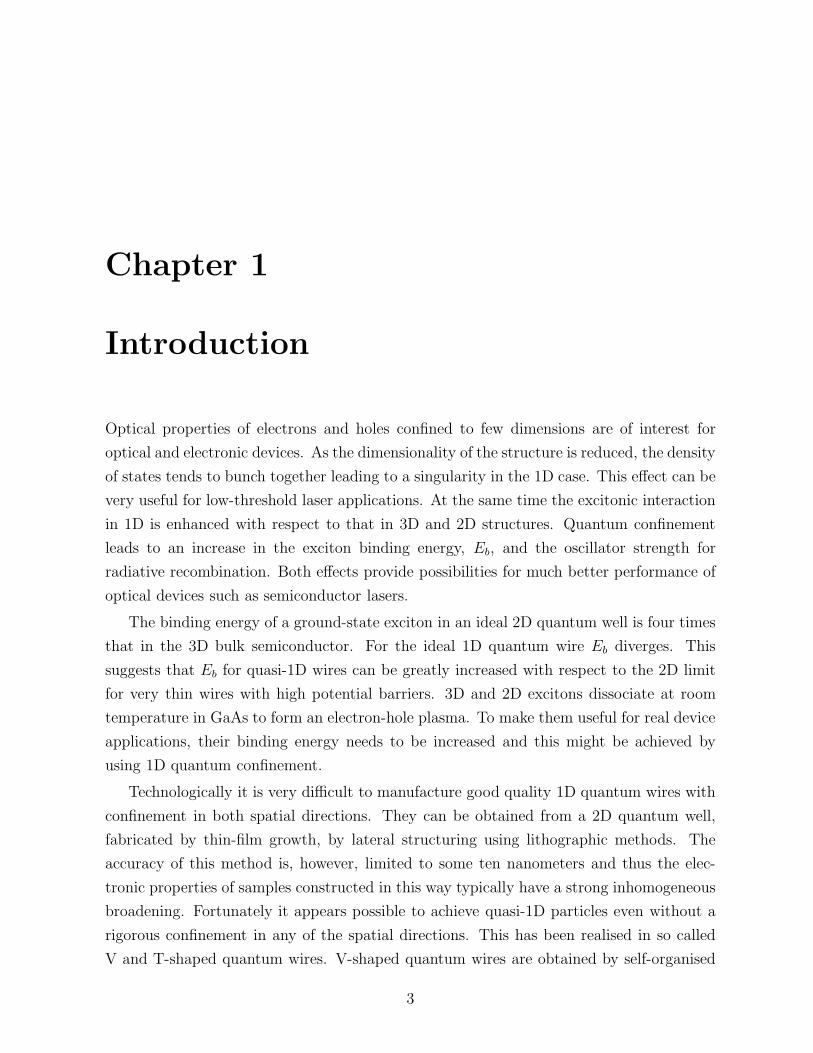
For the 5-nm scale symmetric GaAs/AlAs, Someya et al. [3] reported the largest con-
finement energy for excitons in symmetric wires (Figure 1.1), Econ=38 meV and Eb=27±3
meV. The largest confinement energy of any structure was reported by Gislason et al. [4,5]
for their optimised wires. Using asymmetric wells with different widths and Al content as in
Figure 1.2, they obtained an exciton confinement energy of 54 meV. Recently there has also
been the first experimental realisation of T-shaped wires using InyGa1−yAs/Al0.3Ga0.7As
[2]. The highest confinement energy reported for this structure is 34 meV, which is very
close to the GaAs/AlAs result, and the quality of the structure can be much higher than
for the GaAs/AlAs case.
1. Introduction 5
������������������������������������������������������������������������������������������������������������������������������������������������������������������������������������������������������������������������������������������������������������������������������������������������������������������������������������������������������������������������������������������������������������������������������������������������������������������������������������������������������������������������������������������������������������������������������������������������������������������������������������������������������������������������������������������������������������������������������������������������������������������������
������������������������������������������������������������������������������������������������������������������������������������������������������������������������������������������������������������������������������������������������������������������������������������������������������������������������������������������������������������������������������������������������������������������������������������������������������������������������������������������������������������������������������������������������������������������������������������������������������������������������������������������������������������������������������������������������������������������������������������������������������������������������
������������������������������������������������������������������������������������������������������������������������������������������������������������������������������������������������������������������������������������������������������������������������������������������������������������������������������������������������������������������������������������������������������������������������������������������������������������������������������������������������������������������������������������������������������������������������������������������������������������������������������������������������������������������������������������������������������������������������������������������������������������������������
������������������������������������������������������������������������������������������������������������������������������������������������������������������������������������������������������������������������������������������������������������������������������������������������������������������������������������������������������������������������������������������������������������������������������������������������������������������������������������������������������������������������������������������������������������������������������������������������������������������������������������������������������������������������������������������������������������������������������������������������������������������������
������������������������������������������������������������������������������������������������������������������������������������������������������������������������������������������������������������������������������������������������������������������������������������������������������������������������������������������������������������������������������������������������������������������������������������������������������������������������������������������������������������������������
������������������������������������������������������������������������������������������������������������������������������������������������������������������������������������������������������������������������������������������������������������������������������������������������������������������������������������������������������������������������������������������������������������������������������������������������������������������������������������������������������������������������
1 −xxAl Ga As
Arm
well
Stem well Dy
Dx
GaAs
Figure 1.1: Shape of the symmetric T-shaped wire with notations.
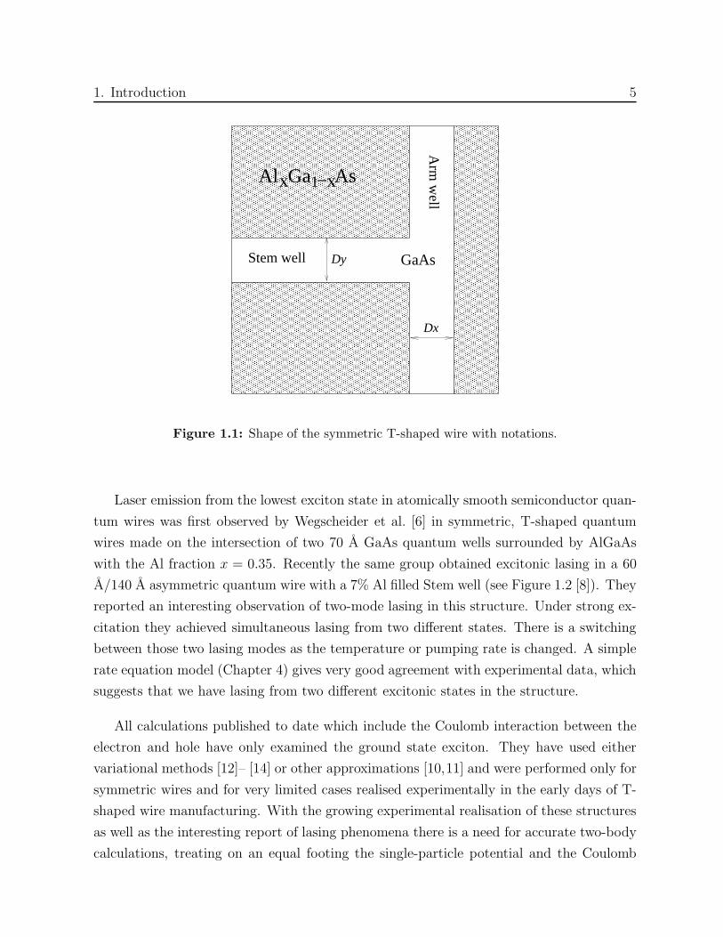
Laser emission from the lowest exciton state in atomically smooth semiconductor quan-
tum wires was first observed by Wegscheider et al. [6] in symmetric, T-shaped quantum
wires made on the intersection of two 70 A GaAs quantum wells surrounded by AlGaAs
with the Al fraction x = 0.35. Recently the same group obtained excitonic lasing in a 60
A/140 A asymmetric quantum wire with a 7% Al filled Stem well (see Figure 1.2 [8]). They
reported an interesting observation of two-mode lasing in this structure. Under strong ex-
citation they achieved simultaneous lasing from two different states. There is a switching
between those two lasing modes as the temperature or pumping rate is changed. A simple
rate equation model (Chapter 4) gives very good agreement with experimental data, which
suggests that we have lasing from two different excitonic states in the structure.
All calculations published to date which include the Coulomb interaction between the
electron and hole have only examined the ground state exciton. They have used either
variational methods [12]– [14] or other approximations [10,11] and were performed only for
symmetric wires and for very limited cases realised experimentally in the early days of T-
shaped wire manufacturing. With the growing experimental realisation of these structures
as well as the interesting report of lasing phenomena there is a need for accurate two-body
calculations, treating on an equal footing the single-particle potential and the Coulomb
6 M. H Szymanska — Bose Condensation and Lasing in Optical Microstructures
����������������������������������������������������������������������������������������������������������������������������������������������������������������������������������������������������������������������������������������������������������������������������������������������������������������������������������������������������������������������������������������������������������������������������������
����������������������������������������������������������������������������������������������������������������������������������������������������������������������������������������������������������������������������������������������������������������������������������������������������������������������������������������������������������������������������������������������������������������������������������
������������������������������������������������������������������������������������������������������������������������������������������������������������������������������������������������������������������������������������������������������������������������������������������������������������������������������������������������������������������������������
������������������������������������������������������������������������������������������������������������������������������������������������������������������������������������������������������������������������������������������������������������������������������������������������������������������������������������������������������������������������������
GaAs
Arm
well
������������������������������������������������������������������������������������������������������������������������������������������������������������������������������������������������������������������������������������������������������������������������������������������������������������������������������������������������������������������������������������������������������������
������������������������������������������������������������������������������������������������������������������������������������������������������������������������������������������������������������������������������������������������������������������������������������������������������������������������������������������������������������������������������������������������������������
35%Al
Dx
7%AlDyStem well
Figure 1.2: Shape of the asymmetric T-shaped wire with notations.
interaction, of both the ground and excited states in the structure.
Excited states seem to be very important for the operation of excitonic lasers [8]. Cal-
culations of energies, oscillator strengths for radiative recombination (i.e, how the various
states couple to photons) as well as the full wave functions for the whole spectra of interest
would be very beneficial for understanding the origins of certain transitions and effects.
This could help in the design of lasers with better properties and higher maximum temper-
atures for excitonic lasing. The goal is to design excitonic lasers which can operate at room
temperature. Also, performing highly accurate calculations of the ground state exciton in
QWR and the corresponding QW enables Eb and Econ to be obtained for different geome-
tries (both symmetric and asymmetric) for a wide range of well widths and Al content, x.
Such data are of great importance for the optimisation of the structures.
In Chapter 2 we present numerical calculations of electron-hole states in a T-shaped
quantum wire. Our method is based on an exact numerical solution of the Schrodinger
equation in a certain basis within the effective mass approximation. The method is not
restricted to a given number of excited states and we can calculate as many of them as
required. For some structures we have calculated up to 100 excited states. We perform
calculations for a very wide range of T-shaped wires. In Section 2.1 the numerical method
1. Introduction 7
is discussed in detail while in Section 2.2 we present the results. There we first study the
spectra and wave functions and present a discussion of the nature of the various excited
states. Finally we discuss Econ, Eb and the difference between the ground-state exciton
energy and the first excited-state energy, E2−1, as a function of well width Dx and Al
molar fraction x for the symmetric and asymmetric quantum wires. Our calculations are
being used to design improved excitonic lasers which will operate at room temperature.
In Chapter 3 we describe an experimental observation of two-mode lasing in a 60 A/140
A asymmetric quantum wire with a 7% Al filled Stem well [8]. This experiment, done at
Bell-Laboratories, was a direct motivation for our work. We have performed the numerical
calculations described in Chapter 2 for samples used in this experiment and have identified
the origin of transitions which correspond to the two lasing modes.
In Chapter 4 we develop a rate equation model for a two-mode laser in which the two
lasing modes come from two different excitonic states in the wire. This model gives very
good agreement with the experimental data described in Chapter 3, which suggests that
we have lasing from two different excitonic states in the quantum wire. The origin of this
excitonic states can be determined from the detail numerical calculations presented for this
experiment in Chapter 3.

Chapter 2
Calculations of the electron-hole
states in T-shaped quantum wires
We calculate energies, oscillator strengths for radiative recombination, and two-particle
wave functions for the ground state exciton and around 100 excited states in a T-shaped
quantum wire. We include the single-particle potential and the Coulomb interaction between
the electron and hole on an equal footing, and perform exact diagonalisation of the two-
particle problem within a finite basis set. We calculate spectra for all of the experimentally
studied cases of T-shaped wires including symmetric and asymmetric GaAs/AlxGa1−xAs
and InyGa1−yAs/AlxGa1−xAs structures. We study in detail the shape of the wave functions
to gain insight into the nature of the various states for selected symmetric and asymmet-
ric wires in which laser emission has been experimentally observed. We also calculate the
binding energy of the ground state exciton and the confinement energy of the 1D quantum-
wire-exciton state with respect to the 2D quantum-well exciton for a wide range of struc-
tures, varying the well width and the Al molar fraction x. We find that the largest binding
energy of any wire constructed to date is 16.5 meV. We also notice that in asymmetric
structures, the confinement energy is enhanced with respect to the symmetric forms with
comparable parameters but the binding energy of the exciton is then lower than in the sym-
metric structures. For GaAs/AlxGa1−xAs wires we obtain an upper limit for the binding
energy of around 25 meV in a 10 A wide GaAs/AlAs structure which suggests that other
materials must be explored in order to achieve room temperature applications. There are
some indications that InyGa1−yAs/AlxGa1−xAs might be a good candidate.
9
10 M. H Szymanska — Bose Condensation and Lasing in Optical Microstructures
2.1 The model
We use the effective mass approximation with an anisotropic hole mass to describe an
electron in a conduction band and a hole in a valence band in the semiconductor structures
under consideration (see Appendix B). The effective mass of the hole depends on the
crystallographic direction in the plane of the T-shaped structure. We consider the heavy
hole only. The other bands (split off bands, light holes) would have energies higher that
the region of interest for us. The light hole exciton, the closest in energy to the heavy
hole exciton, is calculated to be over 30 meV higher that the heavy hole exciton, and thus
it is ignored in the calculations. The electron and hole are in the external potential of
the quantum wire formed at the T-shaped intersection of the GaAs/AlxGa1−xAs quantum
wells. The so called Arm quantum well is grown in the 110 crystal direction and intersects
with a Stem quantum well grown in the 001 direction (see Figures 1.1 and 1.2). In our model
the crystal directions 110, 001, and 110 correspond to x, y, and z respectively. We consider
symmetric quantum wires where the Arm and Stem well are both of the same width, i.e,
Dx = Dy, and are made of GaAs. We also consider asymmetric wires where the Stem well
is significantly wider but filled with AlxGa1−xAs with a low Al content to compensate for
the reduction in confinement energy. Our method is applicable to any structure regardless
of its shape and materials provided the external potential is independent of z
The value of the band-gap is different for the different materials used in the well con-
struction. This gives rise to the potential barriers at the interfaces between the GaAs,
AlxGa1−xAs and InGaAs which take different values for electrons and holes. In our model
the electron and hole are placed in external potentials Ve(x, y) and Vh(x, y), respectively,
and interact via the Coulomb interaction. We choose the potential in GaAs to be zero and
calculate all potentials in other materials with respect to this level. The external potential
is independent of z in all cases. Sample geometries considered in this work are shown in
Figs. 1.1 and 1.2. Using the above model, after the separation of the centre of mass and
relative motion in the z direction, the system is described by the following Hamiltonian:
H = − ~2
2me
∇2xe,ye
− ~2
2mhx
∇2xh
− ~2
2mhy
∇2yh
− ~2
2µz
∇2z + Ve(xe, ye) + Vh(xh, yh)
− e2
4πǫ0ǫ√
(xe − xh)2 + (ye − yh)2 + z2, (2.1)
where z = ze − zh and 1µz
= 1me
+ 1mhz
. The wave function associated with the centre of
2. Calculations of the electron-hole states in T-shaped quantum wires 11
mass motion in the z direction is a plane wave and this coordinate can be omitted from
the problem.
2.1.1 Numerical method for calculating quantum wire exciton
states
We calculate the ground and excited states in the structures of interest by a direct di-
agonalisation method. Due to the complexity of the external potential with its limited
symmetry and sharp edges, none of the standard basis sets seem appropriate. We use the
following basis set:
ψ(xe, ye, xh, yh, ze − zh) =∑
i,j,k
ci,j,k sin(zkπ
Lz
− kπ
2)χe
i (xe, ye)χhj (xh, yh), (2.2)
where χei (xe, ye)/χ
hj (xh, yh) are electron/hole single-particle wave functions for a T-shaped
potential without the electron-hole Coulomb interaction. In the z direction we introduce
hard wall boundary conditions and use a standing-wave basis set.
Our basis set does not obey the so called cusp condition [17] which is satisfied whenever
two particles come together. The divergence in the potential energy when the electron and
hole come together must be exactly cancelled by an opposite divergence in the kinetic
energy. The exact wave function must therefore have a cusp when the electron and hole
are coincident. Using a basis in which every basis function obeys the cusp condition
would reduce the size of the basis set required. For an isotropic hole mass it would be
very easy to satisfy the cusp condition by multiplying the basis functions by the factor
e−Λ√
(xe−xh)2+(ye−yh)2+z2which is just the hydrogenic wave function. Unfortunately there
is no analytical solution when we introduce the anisotropic hole mass. Thus we choose not
to satisfy the cusp condition and therefore have to use a larger basis set.
The diagonalisation is performed using a NAG library routine. Convergence is usually
achieved with a basis set containing 20 of each of the single-particle wave functions and 20
standing waves in the z direction. Thus 20×20×20 = 8000 basis functions are needed which
gives 206 matrix elements. Only one quarter of the total number needs to be calculated as
interchanging k1 and k2 leaves the matrix element unchanged while interchanging i1 and j1
with i2 and j2 gives its complex conjugate. This still leaves a great many matrix elements
to be calculated. Thus to make the calculations feasible the matrix elements need to be
calculated very rapidly (See Section 2.1.3).
12 M. H Szymanska — Bose Condensation and Lasing in Optical Microstructures
2.1.2 Computational Method for Calculating the Single-Particle
Wave Functions
The one-particle (electron and hole) wave functions, χei (xe, ye) and χh
j (xh, yh) in a T-shaped
external potential are calculated using the conjugate-gradient minimisation technique with
pre-conditioning of the steepest descent vector. A detailed explanation of this method
can be found in reference [16]. We specify the external potential on a 2D grid and use
periodic boundary conditions in the x and y directions so that we are able to use Fast
Fourier Transform (FFT) methods to calculate the kinetic energy in Fourier space while
the potential energy matrix elements are calculated in real space. The fast calculation of
the energy matrix elements is crucial as they have to be calculated many times during
the conjugate-gradient minimisation. The FFT provides very fast switching between real
and Fourier space and makes the algorithm much more efficient, but the use of periodic
boundary conditions introduces the problem of inter-cell interactions in the case of two
particle calculations. To avoid this problem we place the unit cell in the middle of another,
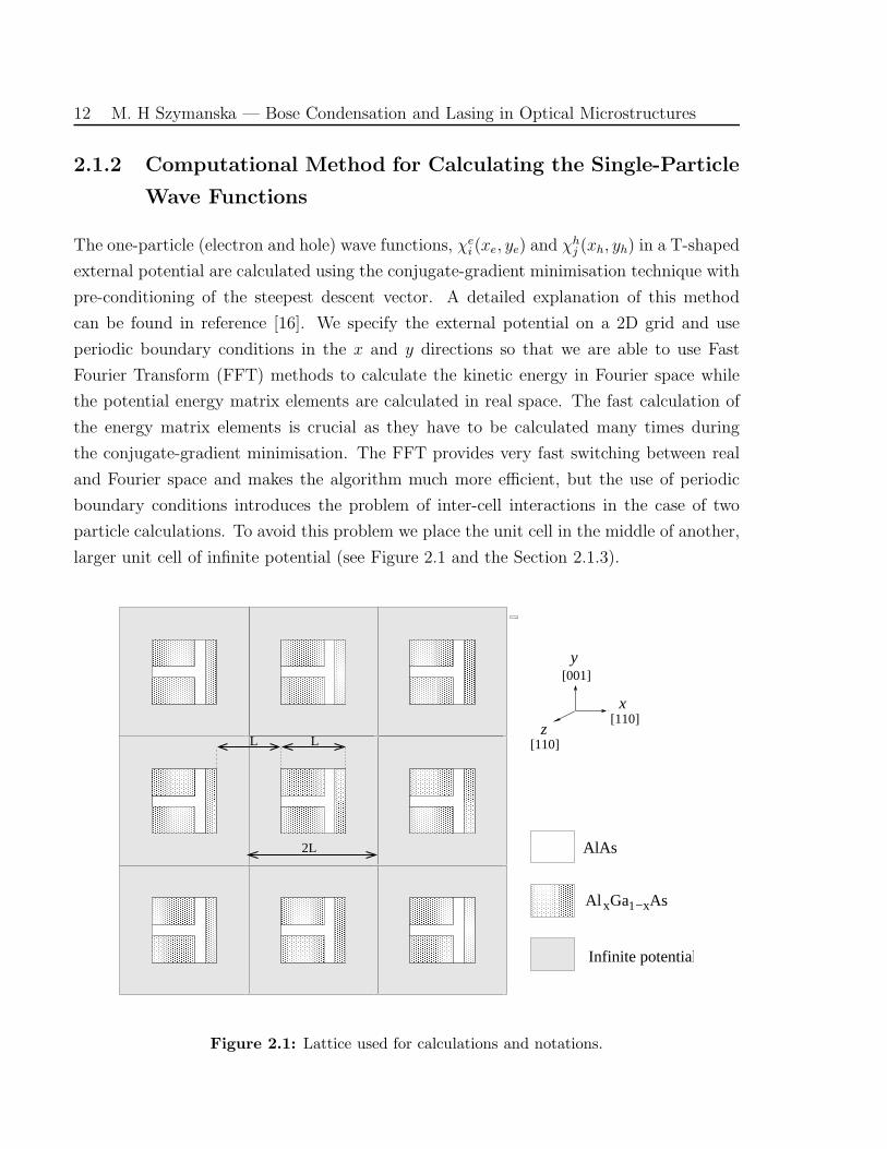
larger unit cell of infinite potential (see Figure 2.1 and the Section 2.1.3).
������������������������������������������
������������������������������������������
������������������������������������������
������������������������������������������
���������������������������������������������
���������������������������������������������
������������������������������������������������
������������������������������������������������
������������������������������������������������
������������������������������������������������
������������������������������������������������
������������������������������������������������
��������������������������������������������������������
��������������������������������������������������������
��������������������������������������������������������
��������������������������������������������������������
��������������������������������
��������������������������������
������������������������������������������������
������������������������������������������������
������������������������������������������������
������������������������������������������������
������������������������������������������������
������������������������������������������������
Infinite potential
Al Ga x 1 −xAs
AlAs
L L
2L
���������������������������������������������������������������
���������������������������������������������������������������
������������������������������������������������
������������������������������������������������
������������������������������������������������
������������������������������������������������
������������������������������������������������
������������������������������������������������
������������������������������������������������
������������������������������������������������
������������������������������������������������
������������������������������������������������
������������������������������������������������
������������������������������������������������
��������������������������������������������������������
��������������������������������������������������������
��������������������������������������������������������
��������������������������������������������������������
��������������������������������
��������������������������������
������������������������������������������
������������������������������������������
�������������������������������������������������
�������������������������������������������������
�������������������������������������������������
�������������������������������������������������
������������������������������
������������������������������
������������������������������������������
������������������������������������������
���������������������������������������������
���������������������������������������������
x
y
[110]z
[110]
[001]
Figure 2.1: Lattice used for calculations and notations.
2. Calculations of the electron-hole states in T-shaped quantum wires 13
We use plane waves as a basis set for the one-particle problem. Using this method
we can calculate as many as 50 states for the electron and 50 for the hole. Very good
convergence with respect to the number of plane waves and the size of the unit cell is
obtained (see Section 2.2.4).
2.1.3 Computational Method for Calculating the Matrix Ele-
ments
The kinetic and potential energies are diagonal in this basis and are obtained from the
one-particle calculations. Thus only the Coulomb matrix elements need to be calculated.
A Coulomb matrix element in the basis set (2.2) is a 5D integral of the following form:
−∫ ∫ ∫ ∫ ∫
dxedyedxhdyhdzsin(zk2π
Lz
− k2π
2)χe∗
i2(xe, ye)χ
h∗j2
(xh, yh)
q(xe − xh, ye − yh, z)sin(zk1π
Lz
− k1π
2)χe
i1(xe, ye)χ
hj1
(xh, yh). (2.3)
Where q(xe−xh, ye−yh, z) is the Coulomb interaction cut off at final distance to avoid image
effects (see below). This integral must be calculated numerically. Numerical integration
for so many dimensions is very slow and thus is not feasible for the case of 206 matrix
elements. Thus another method has to be introduced.
The above integral is of the form
−∫ ∫ ∫ ∫ ∫
dxedyedxhdyhdzfe(xe, ye)fh(xh, yh)q(xe − xh, ye − yh, z)fz(z). (2.4)
Where
fe(xe, ye) = χe∗i2
(xe, ye)χei1(xe, ye),
fh(xh, yh) = χh∗i2
(xh, yh)χhi1(xh, yh),
(2.5)
Using the Fourier transform and the convolution theorem it can be shown that the above
integral is equal to:
∫
dz∑
Gx,Gy
Fe(−Gx,−Gy) ∗ Fh(Gx, Gy) ∗Q(Gx, Gy, z). (2.6)
14 M. H Szymanska — Bose Condensation and Lasing in Optical Microstructures
Where Fe, Fh, Q are the 2D Fourier transforms of the function fe with respect to xe and
ye, fh with respect to xh and yh and q with respect to xe − xh and ye − yh, respectively.
Thus the 5D integral can be reduced to a 1D integral with respect to the z variable and a
2D sum in Fourier space. The Fe and Fh Fourier transforms can be easily calculated using
FFTs in real space after multiplication of the corresponding χei1(xe, ye) by χe∗
i2(xe, ye) for
electrons and χhi1(xh, yh) by χh∗
i2(xh, yh).
In order to use FFTs we need to introduce periodic boundary conditions in the x and
y directions as in the one-particle calculations. To eliminate interactions between particles
in neighbouring cells, we place the unit cell in the middle of another, bigger unit cell of
infinite potential (see Figure 2.1).
The distance between the edges of successive small unit cells is exactly the width of the
small unit cell, L. We cut-off the Coulomb interaction at a distance corresponding to the
size of the small unit cell. We therefor consider the following form of Coulomb interaction:
q(xe − xh, ye − yh, z) =
− e2
4πǫ0ǫ√
(xe−xh)2+(ye−yh)2+z2
if xe − xh < Lx
and ye − yh < Ly
0 otherwise.
(2.7)
Particles interact only when their separations in the x and y directions are smaller than
Lx and Ly respectively. The separations of particles in neighbouring cells is always bigger
than the cut-off and thus they do not interact. Particles in the same unit cell are always
separated by less than that the cut-off distance due to the infinite potential outside the
small unit cell. Thus we take into account all of the physical Coulomb interaction and
completely eliminate the interactions between images. In the numerical implementation
the infinite potential is replaced by a large but finite potential. Thus the probability of the
particle being outside the small unit cell is effectively zero and we find that the results do
not depend on the value of this potential for values greater than around three times the
potential in the AlxGa1−xAs region.
The 2D Fourier transform of the 3D Coulomb interaction with a cut-off cannot be done
analytically. Thus we put the Coulomb interaction onto a 2D grid as a function of relative
coordinates xe − xh and ye − yh for every z value. The unit cell in relative coordinates
will go from −Lx to Lx, and −Ly to Ly respectively. Then for every value of z a 2D FFT
is performed with respect to xe − xh and ye − yh and the results stored in the 3D array
Q(Gx, Gy, z). Since this is the same for every matrix element the above calculation needs
to be performed only once.
2. Calculations of the electron-hole states in T-shaped quantum wires 15
The calculations described by eqn. (2.6) need to be performed for every matrix element.
After Fe(Gx, Gy) and Fh(Gx, Gy) have been calculated the summation over the reciprocal
lattice vectors Gx and Gy for every value of z is performed. The remaining 1D integral in
the z direction is done numerically, after interpolation of data points, using a routine from
the NAG library. The dependence of the integrand on z is found to be very smooth and
thus not many points are required to obtain accurate results.
2.2 Results
We perform the calculations for a series of T-shaped structures. We calculate energies,
oscillator strengths and wave functions for the first 20-100 two-particle states for symmetric
and asymmetric wires.
For symmetric wires we consider the structure denoted by W which has been experimen-
tally studied by Wegscheider et al. [6] and consists of GaAs/Al0.35Ga0.65As 70 A quantum
wells. Then, keeping the rest of parameters constant, we vary the quantum well width from
10 A to 80 A in steps of 10 A in order to examine the width dependence of the various
properties. We also perform calculations for samples denoted by S1 and S2 studied by
Someya et al. [3] made of GaAs/Al0.3Ga0.7As (S1) and GaAs/AlAs (S2) quantum wells of
width around 50 A. For the GaAs/AlAs case we again vary the well width from 10 A to
60 A. Then we take an intermediate value of the Al molar fraction, x = 0.56, and vary the
well width from 10 A to 60 A in order to examine the dependence on the well width as well
as Al content. Finally we perform calculations for 35 A-scale In0.17Ga0.83As/Al0.3Ga0.7As
(denoted by N4) as well as for 40 A-scale In0.09Ga0.91As/Al0.3Ga0.7As (denoted by N2)
samples as studied experimentally by Akiyama et al. [2].
For asymmetric structures we consider the wire studied experimentally by Rubio et
al. [8] which consists of a 60 A GaAs/Al0.35Ga0.65As Arm quantum well and a 140 A
Al0.07Ga0.93As/Al0.35Ga0.65As Stem quantum well. We vary the width of the Arm quantum
well from 50 A to 100 A. We also perform calculations for the asymmetric structure studied
by a different group [4, 5] which consists of a 25 A GaAs/Al0.3Ga0.7As Arm quantum well
and a 120 A Al0.14Ga0.86As/Al0.3Ga0.7As Stem quantum well.
In the first part of this section we present the spectra for symmetric and asymmetric
quantum wires with the positions of 2D exciton, 1D continuum (unbound electron and hole
both in the wire) and 1De/2Dh continuum (unbound electron in the wire and hole in the
well) states as well as pictures of representative wave functions. This allows us to discuss
16 M. H Szymanska — Bose Condensation and Lasing in Optical Microstructures
the nature of the excited states in the structures. In the second part we discuss the trends
in confinement and binding energy and the separation in energy between the ground and
the first excited states as a function of the well width and Al fraction.
We use a static dielectric constant ǫ=13.2 and a conduction band offset ratio Qc =
∆Econd/∆Eg of 0.65. For the difference in bandgaps on the GaAs/AlxGa1−xAs interface we
use the following formula: ∆Eg = 1247×xmeV for x < 0.45 and 1247×x+1147×(x−0.45)2
meV for x > 0.45. For the electron mass we use me = 0.067m0 while for the hole
mass mhx = mhz = mh[110] = 0.69 − 0.71m0 and mhy = mh[001] = 0.38m0 (m0 is
the electron rest mass). For the In0.09Ga0.91As/Al0.3Ga0.7As (In0.17Ga0.83As/Al0.3Ga0.7As)
we use parameters from reference [2]: for the electron me = 0.0647(0.0626)m0, for the
hole mhy = mhh[001] = 0.367(0.358)m0 and mhx = mhz = mh[110] = 0.682(0.656)m0,
∆Eg=464(557) meV and the band offset was assumed to be 65% in the conduction and
35% in the valence band.
2.2.1 Excited States
Symmetric Wires
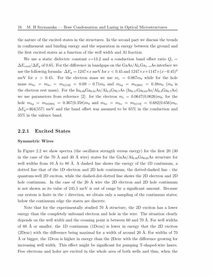
In Figure 2.2 we show spectra (the oscillator strength versus energy) for the first 20 (30
in the case of the 70 A and 30 A wire) states for the GaAs/Al0.35Ga0.65As structure for
well widths from 10 A to 80 A. A dashed line shows the energy of the 1D continuum, a
dotted line that of the 1D electron and 2D hole continuum, the dotted-dashed line - the
quantum-well 2D exciton, while the dashed-dot-dotted line shows the 2D electron and 2D
hole continuum. In the case of the 20 A wire the 2D electron and 2D hole continuum
is not shown as its value of 245.5 meV is out of range by a significant amount. Because
our system is finite in the z direction, we obtain only a sampling of the continuum states;
below the continuum edge the states are discrete.
Note that for the experimentally studied 70 A structure, the 2D exciton has a lower
energy than the completely unbound electron and hole in the wire. The situation clearly
depends on the well width and the crossing point is between 60 and 70 A. For well widths
of 60 A or smaller, the 1D continuum (1Dcon) is lower in energy that the 2D exciton
(2Dexc) with the difference being maximal for a width of around 20 A. For widths of 70
A or bigger, the 1Dcon is higher in energy than the 2Dexc with the difference growing for
increasing well width. This effect might be significant for pumping T-shaped-wire lasers.
Free electrons and holes are excited in the whole area of both wells and thus, when the
2. Calculations of the electron-hole states in T-shaped quantum wires 17
95 100 105 110 115 120 125 130 135
=40 ÅDx
50 55 60 65 70 75 80
=60 ÅDx
30 35 40 45 50 55
=80 ÅDx
315 320 325 330 335 340 345 3500
2
4
6
8
10
12
14
16
1D con
2D exc
1De/2Dhcon 2De/2Dhcon
=10 ÅDx
135 140 145 150 155 160 165 170 175 1800
2
4
6
8
10
12
14
16 =30 ÅDx
40 45 50 55 60 650
2
4
6
8
10
1
2527
15 22
=70 Å
2
Dx
70 75 80 85 90 95 100 1050
2
4
6
8
10=50 ÅDx
E (MeV)
−3
nm)
Osc
illat
or s
tren
gth
(10 4
Figure 2.2: Oscillator strength versus energy for the lowest 20-30 states in a symmetricT-shaped structure for different well widths Dx.
18 M. H Szymanska — Bose Condensation and Lasing in Optical Microstructures
2D exciton has a lower energy than the 1D continuum, formation of the 2D excitons is
energetically favourable. These excitons can recombine in a well instead of going to the
wire and forming a 1D exciton. Clearly it is more efficient to have the 1D continuum lower
in energy than the 2D exciton.
By increasing the well width we obtain more states that are lower in energy than the
1Dcon and 2Dexc beginning with two (ground and the first excited) for the 10 A well,
three for widths between 20-50 A and four states for larger widths.
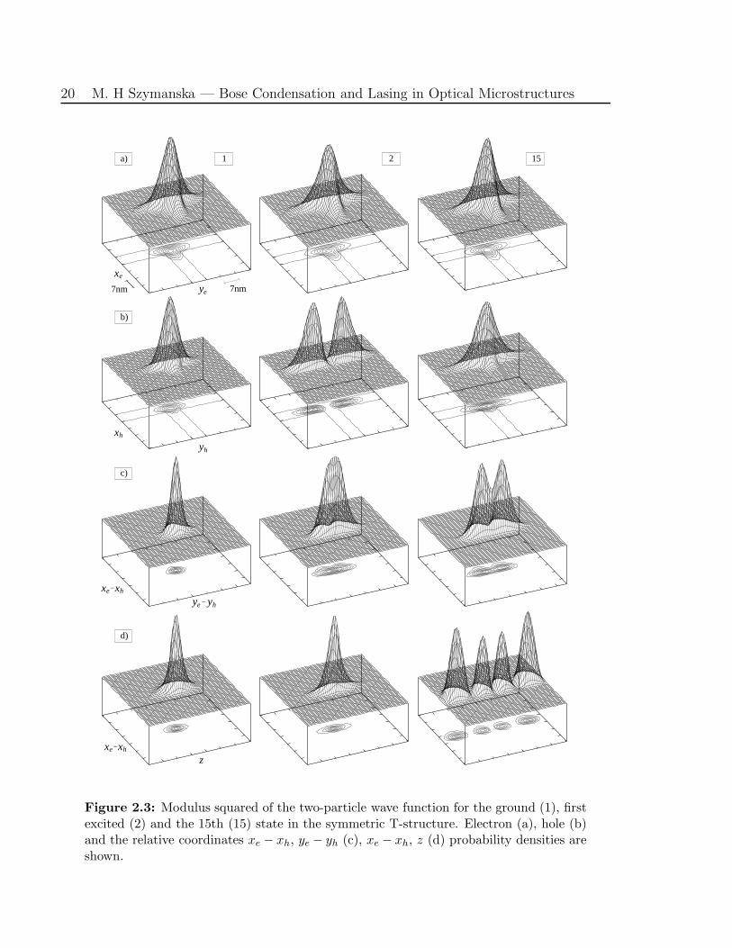
We now discuss the behaviour of |ψ|2 for the 70 A case. The wave functions depend on
five spatial coordinates and thus various cuts in 5D space are presented in Figures 2.3 and
2.4: a) the electron xe, ye position after averaging over the hole position, b) the hole xh, yh
position after averaging over the electron position, and relative coordinates after averaging
over the centre of mass position c) the xe − xh, ye − yh relative coordinates for ze − zh = 0
and d) the xe − xh, z relative coordinates for ye − yh = 0.
For the ground state we observe that the electron and hole are very well localised in
the wire with slightly more hole localisation. The relative coordinate plots clearly show
the bound exciton (Figure 2.3(1)).
The electron in the first excited state is localised in the wire while the hole already
expands into the Arm well. The relative coordinate pictures show that the electron and
hole are bound and form an exciton with an asymmetric shape. The size of the exciton
is smallest in the x direction (the Stem well direction) and the exciton expands more into
the y (the Arm well where the hole is expanded) and free z directions (Figure 2.3 (2)).
The oscillator strength of this state is about 1/3 of that of the ground state and the state
clearly takes the form of a 1D exciton with its centre of mass in the T-wire.
It can be seen from the spectra (Figure 2.2) that there are four states (apart from the
ground state) with energies smaller than 1Dcon and 2Dexc. The nature of the 3rd and 5th
states is very similar to the 2nd one: the centre of mass is in the wire and the electron is
still well localised in the wire while the hole spreads into the wells (into both the Arm and
Stem wells for the 3rd state while only into the Stem well for the 5th one). The relative
coordinates show the complex, asymmetric shape of this excitonic state and the oscillator
strength is again around 1/3 of the ground state exciton.
The 4th state with almost zero oscillator strength corresponds to a 1D continuum. The
electron and hole are both in the wire but the relative coordinate pictures show an unbound
exciton. Within the first 30 states we have 3 states of that nature: the 4th, 7th and 15th.
The 15th state is shown in Figure 2.3: the electron and hole are confined in the wire (a,
2. Calculations of the electron-hole states in T-shaped quantum wires 19
b) and there are 3 nodes in the z direction and 1 node in the y direction. The other two
states look similar and differ only in the number of nodes. The energy of the 4th state,
which is the lowest 1Dcon state, turns out to be lower than the real 1Dcon obtained from
our one-particle calculations. This is due to the finite size effects. Our method is very
well converged with respect to the cell size for the bound state and for the unbound ones
where at least one of the particles is in the well. However, for the unbound continuum 1D
states, the particles are very close in the x, y plane because of the very small size of the
wire and thus the interaction is stronger. Consequently it does not decay as fast in the
z direction as other states and thus we need a much bigger unit cell in the z direction to
achieve convergence. There are however only three such states within the 30 we examine
and we know their true energies from the preceding one particle calculations.
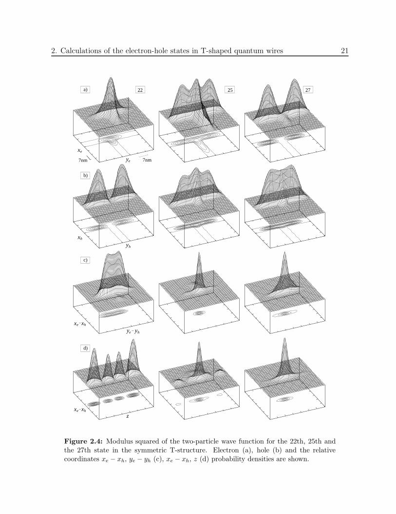
For further excited states up to the 25th, the electron, and thus the centre of mass,
is still localised in the wire while the hole is taking up more and more energetic states in
both wells, where energies are quantised due to the finite size of the cell. Those states can
be divided into two groups depending on their relative coordinate nature: excitonic-like
states similar to the second state (Figure 2.3 (2)) and ionised states like the 22nd which
is represented in Figure 2.4 (22). The oscillator strength of the second group is zero (see
Figure 2.2).
The 25th state (Figure 2.4 (25)) is the first state where the electron is de-localised in
both wells, the relative coordinates and the large oscillator strength shows that it is clearly
an excitonic-like state. It appears to be a 2D quantum well exciton state scattered on the
T shaped intersection. Its energy is thus higher than that of a pure 2Dexc.
The 27th state is the 2D Arm-quantum-well-exciton state. It has higher energy than
the ground-state 2D exciton because the electron and hole wave functions occupy higher
energy states than the ground state of the well due to the presence of the T intersection.
The 30th state has a very similar nature to the 27th but the exciton expands into the
Stem instead of the Arm quantum well.
The 25th, 27th and 30th states all have large oscillator strengths (around 3/4 of that of
the ground state exciton). It is interesting to note that between the ground state and those
2D large-oscillator-strength states, there is a group of states with relatively low oscillator
strengths. The reason for this is that after the ground state, there are states where either
the wire-like electron is bound to the well-like hole and thus they do not overlap enough
to give big contribution to the spectrum or they consist of a wire like electron with an
unbound hole.
20 M. H Szymanska — Bose Condensation and Lasing in Optical Microstructures
����������������
�����������
������������� ����
xh
xe xh−
yhye −
y
x
ye
xh−e
h
z
���������
���������
x
7nm
15
e
7nm����
a)
b)
c)
d)
1 2
Figure 2.3: Modulus squared of the two-particle wave function for the ground (1), firstexcited (2) and the 15th (15) state in the symmetric T-structure. Electron (a), hole (b)and the relative coordinates xe − xh, ye − yh (c), xe − xh, z (d) probability densities areshown.
2. Calculations of the electron-hole states in T-shaped quantum wires 21
����
�����������
������������� ����
yh
xh
yhye −
xe xh−
xe xh−
e
e
x
y
z
���������
���������
����������������
7nm
d)
7nm
22 25 27a)
b)
c)
Figure 2.4: Modulus squared of the two-particle wave function for the 22th, 25th andthe 27th state in the symmetric T-structure. Electron (a), hole (b) and the relativecoordinates xe − xh, ye − yh (c), xe − xh, z (d) probability densities are shown.
22 M. H Szymanska — Bose Condensation and Lasing in Optical Microstructures
Those quantum-well-like exciton states that scattered on the T-shaped potential (like
state 25) appear to be quite important for the excitonic lasing because of their big oscillator
strength. In [8] the authors reported two-mode lasing in an asymmetric wire where the laser
switches between the ground-state exciton and the other state whose energy corresponds
to the state from the tail of the above mentioned states.
Asymmetric Wires
The asymmetric wire that we study in detail consists of a 60 A or 56 A GaAs/Al0.35Ga0.65As
Arm quantum well and a 140 A Al0.07Ga0.93As/Al0.35Ga0.65As Stem quantum well [8]. The
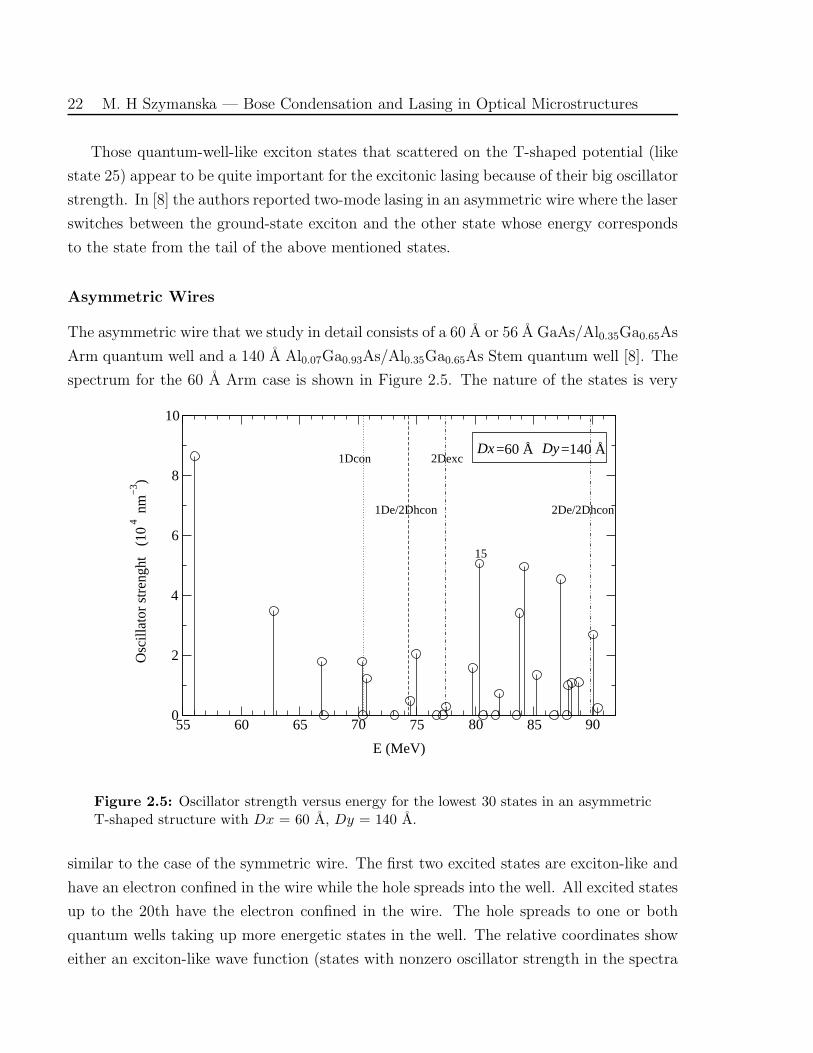
spectrum for the 60 A Arm case is shown in Figure 2.5. The nature of the states is very
55 60 65 70 75 80 85 90
E (MeV)
0
2
4
6
8
10
Osc
illat
or s
tren
ght
(10 4
nm
−3 )
1Dcon 2Dexc
15
1De/2Dhcon 2De/2Dhcon
=140 Å=60 ÅDx Dy
Figure 2.5: Oscillator strength versus energy for the lowest 30 states in an asymmetricT-shaped structure with Dx = 60 A, Dy = 140 A.
similar to the case of the symmetric wire. The first two excited states are exciton-like and
have an electron confined in the wire while the hole spreads into the well. All excited states
up to the 20th have the electron confined in the wire. The hole spreads to one or both
quantum wells taking up more energetic states in the well. The relative coordinates show
either an exciton-like wave function (states with nonzero oscillator strength in the spectra
2. Calculations of the electron-hole states in T-shaped quantum wires 23
of Figure 2.5) or the case where a hole is confined in the wire but is not bound to the
electron (states with zero oscillator strength in the spectra). Both groups were discussed
and shown for the symmetric wire.
The 21st and the 24th states (large oscillator strengths in the Figure 2.5) have an
electron expanding into the Arm well. The electron wave function has a node in the wire
region. The hole wave function spreads into the Arm well and has no node for the 21st
state and one node in the wire region for the 24th state. The relative coordinates show the
excitonic nature of these states. Thus these states correspond to those 2D excitonic states
scattered on the wire.
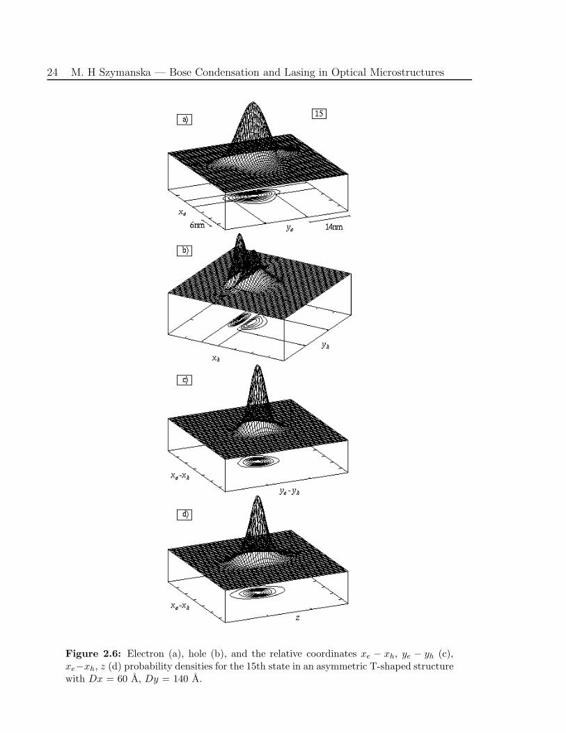
For the asymmetric structure we observe one state (the 15th, see Figure 2.6) which
does not correspond to any state in the symmetric case. The state is clearly excitonic-like
with a large oscillator strength and the relative coordinate plots show a very well bound
exciton. The electron is confined in the wire in the same way as the ground state while the
hole is clearly 1D-like, strongly confined in the wire but in a different way. It has a node
in the wire region.
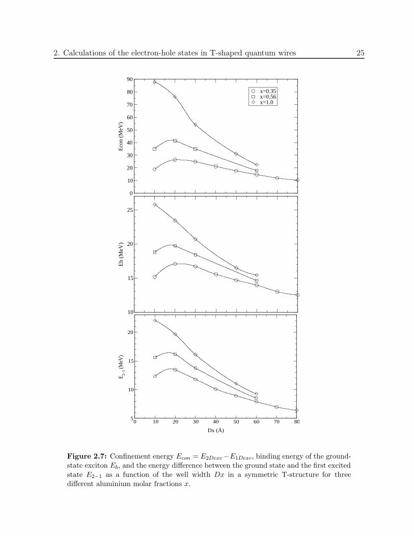
2.2.2 Trends in Confinement and Binding Energies
Symmetric Wires
We calculate the exciton binding energy, Eb = Ee + Eh − E1Dexc, where Ee and Eh are
the one-particle energies of an electron and a hole, respectively, in the wire. We also
calculate, using the same method, the exciton energy in the quantum well, E2Dexc, to
obtain the confinement energy of the 1D exciton, Econ = E2Dexc −E1Dexc, in the wire. We
perform calculations for a wide range of structural parameters. For the GaAs/AlxGa1−xAs
quantum wire we change the well width from 10 A to 80 A for three different values of the
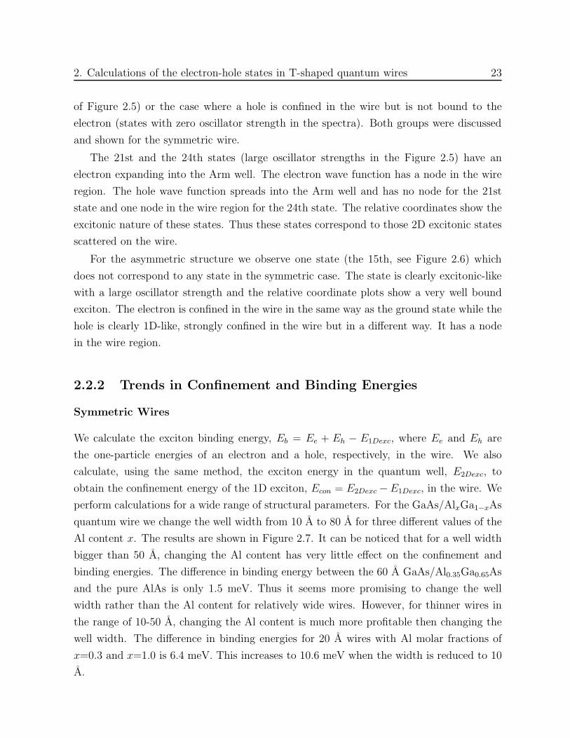
Al content x. The results are shown in Figure 2.7. It can be noticed that for a well width
bigger than 50 A, changing the Al content has very little effect on the confinement and
binding energies. The difference in binding energy between the 60 A GaAs/Al0.35Ga0.65As
and the pure AlAs is only 1.5 meV. Thus it seems more promising to change the well
width rather than the Al content for relatively wide wires. However, for thinner wires in
the range of 10-50 A, changing the Al content is much more profitable then changing the
well width. The difference in binding energies for 20 A wires with Al molar fractions of
x=0.3 and x=1.0 is 6.4 meV. This increases to 10.6 meV when the width is reduced to 10
A.
24 M. H Szymanska — Bose Condensation and Lasing in Optical Microstructures
Figure 2.6: Electron (a), hole (b), and the relative coordinates xe − xh, ye − yh (c),xe−xh, z (d) probability densities for the 15th state in an asymmetric T-shaped structurewith Dx = 60 A, Dy = 140 A.
2. Calculations of the electron-hole states in T-shaped quantum wires 25
0
10
20
30
40
50
60
70
80
90
Eco
n (M
eV)
x=0.35x=0.56x=1.0
10
15
20
25
Eb
(M
eV
)
0 10 20 30 40 50 60 70 80
Dx (Å)
5
10
15
20
E 2−1 (M
eV)
Figure 2.7: Confinement energy Econ = E2Dexc−E1Dexc, binding energy of the ground-state exciton Eb, and the energy difference between the ground state and the first excitedstate E2−1 as a function of the well width Dx in a symmetric T-structure for threedifferent aluminium molar fractions x.
26 M. H Szymanska — Bose Condensation and Lasing in Optical Microstructures
Eb and Econ for Al contents of x=0.35 and x=0.56 both approach a maximum for a
well width between 10 A and 20 A. The maximum values for x=0.35 are Ebmax = 17.1
meV, Econmax = 26.4 meV and for x=0.56 they are Ebmax = 19.7 meV, Econmax = 41.4
meV. For the x=1.0 case, the curve does not have a maximum in the region for which
calculations has been performed but we consider going to wells thinner than 10 A as
practically uninteresting. Thus the maximum energies are for Dx=10 A and they are
Ebmax = 25.8 meV and Econmax = 87.8 meV.
Econ increases much more rapidly than Eb when the well width is progressively reduced.
The curves cross for a well width between 60 A and 70 A, i.e. for widths of 60 A or smaller,
Econ is greater that Eb which means that the 1D continuum is lower in energy than the
2D exciton (as we discussed in section 2.2.1) with the difference having a maximum at
around 20 A. For widths of 70 A or bigger, Eb is greater than Econ with the difference
growing for increasing well width. We also consider the difference in energy between the
ground state exciton in the wire and the first excited state as a function of the well widths.
For the experimentally realised Dx = 70 A case, this difference is E2−1 = 7.0 meV and
the maximum value for Dx = 10 A is E2−1max = 13.5 meV. The maximum value for the
GaAs/AlAs at Dx = 20 A is 22 meV.
Although pure AlAs gives the biggest potential offsets and thus the biggest binding and
confinement energies, the GaAs/AlAs interfaces are not very smooth, which influences the
transport properties. Thus new materials have to be proposed. Two structures based on
InGaAs have been manufactured and measured [2]: 35 A-scale In0.17Ga0.83As/Al0.3Ga0.7As
(N4) and 40 A-scale In0.09Ga0.91As/Al0.3Ga0.7As (N2). The results of calculations for these
structures are presented in Table 2.1. It can be seen that energies for the sample N4 are
almost exactly the same as for the GaAs/AlAs sample S2 suggesting that these materials
might be very good candidates for structures with large exciton confinement and binding
energies.
Asymmetric Wires
In order to increase binding and confinement energies, the asymmetric T-shaped structure
was proposed and realised by two groups [4, 5, 8].
We calculate Eb and Econ for the 60 A/140 A structure with the Stem quantum well
filled with 7% Al in order to compare with experiment [8] and then we vary the width of the
Arm well from 50 to 100 A. One can see from Figure 2.8 that the binding energy is almost
independent of the Arm well width in this region, changing only from the maximum value
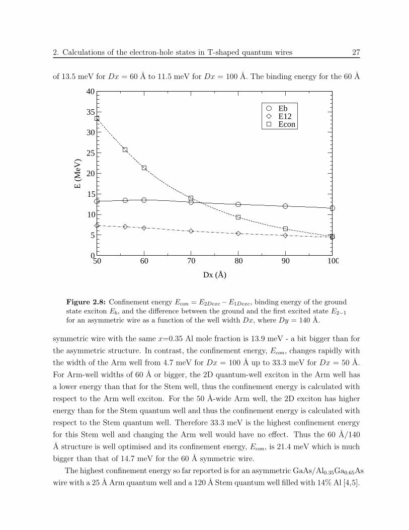
2. Calculations of the electron-hole states in T-shaped quantum wires 27
of 13.5 meV for Dx = 60 A to 11.5 meV for Dx = 100 A. The binding energy for the 60 A
50 60 70 80 90 100
Dx (Å)
0
5
10
15
20
25
30
35
40
E (
MeV
)
EbE12Econ
Figure 2.8: Confinement energy Econ = E2Dexc −E1Dexc, binding energy of the groundstate exciton Eb, and the difference between the ground and the first excited state E2−1
for an asymmetric wire as a function of the well width Dx, where Dy = 140 A.
symmetric wire with the same x=0.35 Al mole fraction is 13.9 meV - a bit bigger than for
the asymmetric structure. In contrast, the confinement energy, Econ, changes rapidly with
the width of the Arm well from 4.7 meV for Dx = 100 A up to 33.3 meV for Dx = 50 A.
For Arm-well widths of 60 A or bigger, the 2D quantum-well exciton in the Arm well has
a lower energy than that for the Stem well, thus the confinement energy is calculated with
respect to the Arm well exciton. For the 50 A-wide Arm well, the 2D exciton has higher
energy than for the Stem quantum well and thus the confinement energy is calculated with
respect to the Stem quantum well. Therefore 33.3 meV is the highest confinement energy
for this Stem well and changing the Arm well would have no effect. Thus the 60 A/140
A structure is well optimised and its confinement energy, Econ, is 21.4 meV which is much
bigger than that of 14.7 meV for the 60 A symmetric wire.
The highest confinement energy so far reported is for an asymmetric GaAs/Al0.35Ga0.65As
wire with a 25 A Arm quantum well and a 120 A Stem quantum well filled with 14% Al [4,5].
28 M. H Szymanska — Bose Condensation and Lasing in Optical Microstructures
The experimentally obtained Econ for this structure is 54 meV. Our calculations however
give only 36.4 meV which is still the highest among experimentally obtained structures
but much lower than reported by the authors. Our calculation of Econ for five different
experimentally realised structures agree very well with the experimental values and thus it
is very probable that the value of 54 meV is overestimated. The binding energy from our
calculations is only 14.6 meV for this structure.
We can conclude from our results that the optimised asymmetric structure does not
lead to a bigger exciton binding energy than the symmetric ones with the same parameters.
The confinement energy is considerably enhanced and this effect, which can be measured
directly, has often been used to infer that the binding energy is increased. However,
our results show that no such relationship holds between the confinement and binding
energies. Thus the biggest confinement energy of any structure constructed so far of 36.4
meV does not lead to the biggest binding energy. Indeed, the binding energy of 14.6 meV is
smaller than the 16.5 meV reported for the GaAs/AlAs 50 A-scale symmetric structure [3]
where the confinement energy should be only 31.1 meV. It is also smaller than expected
for a symmetric 25 A-scale structure with the same parameters (16.0-16.5 meV). Thus
asymmetric structures could be useful for applications where a large confinement energy is
required but appear to be less suitable than symmetric wires for applications where large
binding energies are of interest.
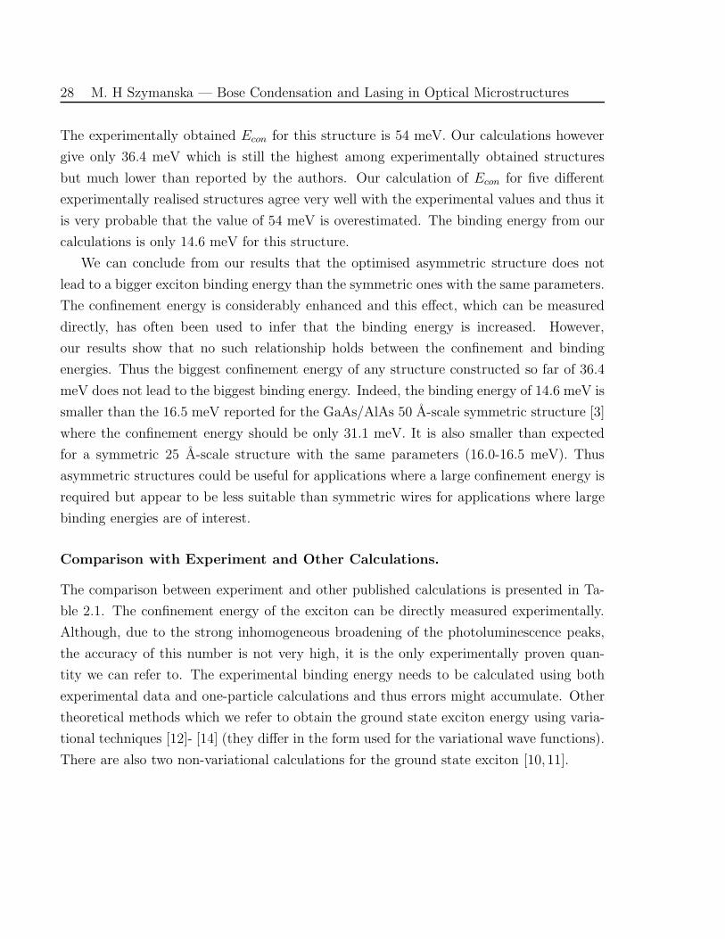
Comparison with Experiment and Other Calculations.
The comparison between experiment and other published calculations is presented in Ta-
ble 2.1. The confinement energy of the exciton can be directly measured experimentally.
Although, due to the strong inhomogeneous broadening of the photoluminescence peaks,
the accuracy of this number is not very high, it is the only experimentally proven quan-
tity we can refer to. The experimental binding energy needs to be calculated using both
experimental data and one-particle calculations and thus errors might accumulate. Other
theoretical methods which we refer to obtain the ground state exciton energy using varia-
tional techniques [12]- [14] (they differ in the form used for the variational wave functions).
There are also two non-variational calculations for the ground state exciton [10, 11].
2.C
alculation
sof
the
electron-h
olestates
inT
-shap
edquan
tum
wires
29
Table 2.1: Binding energy, Eb and the confinement energy Econ = E1Dexc −E2Dexc in meV of the QWR exciton for sevendifferent samples W,S1, S2, N2, N4, R and G obtained from different methods.
Wa S1b S2
b N2c N4
c Rd Ge
Method Eb Econ Eb Econ Eb Econ Eb Econ Eb Econ Eb Econ Eb Econ
Expf 17 17 17 18 27 38 28 34 13.8 23 54This work 13 12 14.3 17.8 16.5 31.1 12.1 26.3 16.5 31.2 13.5 21.4 14.6 36.4Nonvar1g 13.2 14.3 16.4Nonvar2h 11.63 13.9Var1i 15 18Var2j 9.6 11.9Var3k 12 14
a Sample and experimental values from Ref. [6].b Sample and experimental values from Ref. [3].c Sample and experimental values from Ref. [2].d Sample and experimental values from Ref. [8].e Sample and experimental values from Ref. [4, 5].f Econ is obtained experimentally from the shift between QW and QWR exciton lines.
The Eb is obtained indirectly from experimental measurement of the QWR exciton line and one-particle calculations.g Results of calculations from Ref. [10].h Results of calculations from Ref. [11].i Results of variational calculations from Ref. [12].j Results of variational calculations from Ref. [13].k Results of variational calculations from Ref. [14].
30 M. H Szymanska — Bose Condensation and Lasing in Optical Microstructures
Our results for the confinement energy of the ground state exciton Econ agree very well
with experimental values for samples S1, N2 and N4 to an accuracy of 1%, 6% and 8%
respectively. This is indeed very good agreement taking into account the strong inhomoge-
neous broadening of the peaks they present. The spectral linewidth of the photolumines-
cence peaks according to the authors is around 15 meV which corresponds to a thickness
fluctuation of about 3 A for N2 and N4 [2]. For the S1 and S2 samples the authors esti-
mate the experimental error due to the inhomogeneous broadening as 2 meV. Agreement
between our calculations and experiment is not as good for the S2 sample but for this case
additional effects are present. For example, AlAs barriers give much less smooth interfaces
than the lower Al fraction samples and this is not taken into account in our model. There
is also very good agreement (better then 7%) between our results and the experimental
measurement [8] for asymmetric wire R. The earlier Econ published by this group for the
symmetric structure W is probably slightly overestimated.
All calculations published to date use the effective mass approximation model for the
heavy-hole exciton. Values of potential barriers used in the calculations vary depending on
the publication. We have examined the influence of these differences on the final results
(see Section 2.2.4). Both binding and confinement energies can differ by approximately 0.5
meV
There are only two calculations published for the confinement energy. They are based
on variational methods and were performed only for sample W. Variational method 2 [13]
uses a wave function which takes into account correlation in all spatial direction and the
agreement with our results is very good for the confinement energy but not so good for the
binding energy.
The variational method proposed by Kiselev et al. [14] and denoted here by “3” has a
trial wave function which has only z dependence in the correlation factor. Their binding
energy for the sample W differs by only 1 meV from our result but their value for the
confinement energy differs from ours. They perform calculations of the binding energy
for the whole range of well widths, Dx, from 10-70 A. This can be compared with our
results in Figure 2.7. Their calculations, like ours, give the maximum for Eb and Econ
for a well width of around 20 A. Their binding energy is a bit bigger than the one from
our calculations. They obtained a maximum of Eb = 18.6 meV which is 1.5 meV higher
than our result. However, their confinement energy Econmax = 33.0 meV differs by 7 meV
from our result. Their values of Econ are probably overestimated. They use the variational
technique to calculate the quantum wire exciton energy but the quantum well exciton
2. Calculations of the electron-hole states in T-shaped quantum wires 31
energy is taken from some other calculations of excitons in quantum wells performed using
a different method and with different parameters, thus errors may accumulate.
The variational method 1 [12], which uses yet another form of trial wave function, has
been applied to samples S1 and S2 to calculate the binding energy Eb. It agree quite well
with our and other accurate methods.
The binding energy we obtain shows excellent agreement with another non-variational
calculations by Glutsch et al. [10] (see Table 2.1). They calculated the binding energy
only for samples W, S1 and S2 and thus unfortunately the confinement energy cannot be
compared. The method presented in reference [11] gives much lower values for the binding
energy than all other methods.
Despite some small differences, all of the theoretical methods give much smaller values
for Eb than the experimental estimates. One has to bear in mind, however, that the “exper-
imental” values for Eb (quoted in the Table 2.1) are in fact derived from a combination of
experimental data and associated theoretical modelling, with inherent uncertainties. Our
results come from direct diagonalisation and are very well converged. Therefore we believe
that the experimental binding energies are, in some cases, considerably overestimated. The
real binding energy is thus smaller than has been claimed and the biggest value for any of
the structures manufactured so far is 16.5 meV for samples S2 and N4.
2.2.3 Optimisation of Confinement Energy for Experimental Re-
alisation
In Section 2.2.2 we have shown that for symmetric GaAs/AlxGa1−xAs wires the upper
limit for the binding energy is around 25 meV. We have also shown that in asymmetric
structures, the confinement energy is enhanced with respect to the symmetric forms with
comparable parameters but the binding energy of the exciton is then lower than in the
symmetric structures. The upper bound of 25 meV is too low for the room temperature
applications. There are some indications (Section 2.2.2) that InyGa1−yAs/AlxGa1−xAs
might be a good candidate.
Good quality GaAs/AlxGa1−xAs wires are, however, much easier to manufacture that
the InyGa1−yAs/AlxGa1−xAs ones, which brings a considerable interest in optimising the
confinement energy for the GaAs/AlxGa1−xAs wires. The form of the density of states for
electrons and holes in 1D (see Chapter 1) is very useful for low-threshold laser applications.
Therefore structures in which excitons dissociate at room temperature but remain in the
wire would also be relevant for practical applications.
32 M. H Szymanska — Bose Condensation and Lasing in Optical Microstructures
We collaborate with experimentalists from Bell-Laboratories to design such lasers. The
optimisation of the confinement energy of excitons is a crucial issue in this design. We have
shown in Section 2.2.2 that in the asymmetric T-shaped wires, the confinement energy is
enhanced with respect to the symmetric forms, with comparable parameters. We will try
now to optimise the GaAs/AlxGa1−xAs asymmetric wires within the well thickness and Al
concentration range accessible by experiment.
We perform calculations for structures shown in Figure 1.2 with a 140 A, 120 A and
100 A Stem well filled with 7 %, 10 % and 13 % Al respectively. For all four different Stem
wells we vary the width of the Arm well for four different potential barriers corresponding
to 100 %, 70 %, 50 % and 35 % of Al content. The Arm well width is varied from 90 A
to around the value for which Econ has a maximum. For each structure this maximum
corresponds to the case in which exciton energies in the Arm and Stem quantum wells are
equal. When the width of the Arm well is decreased further the Arm well exciton energy
increases, causing the exciton to spread more into the Stem well and reducing the quantum
confinement.
The binding energy of excitons does not vary much within the studied range and it
changes from 17 meV for a wire which consists of a 100 A/ 13 % Stem well, 40 A Arm well
and 100 % Al barriers to 12 meV for a wire with a 140A/ 7 % Stem well, 90 A Arm well
and 35 % Al barriers. The values of Eb for these wires are also slightly smaller than for
the corresponding symmetric structures (see Figure 2.8 - upper panel). The confinement
energy, however, is much enhanced with respect to the symmetric forms (see Figure 2.8
- middle panel) and strongly depends on its parameters. The results of our calculations
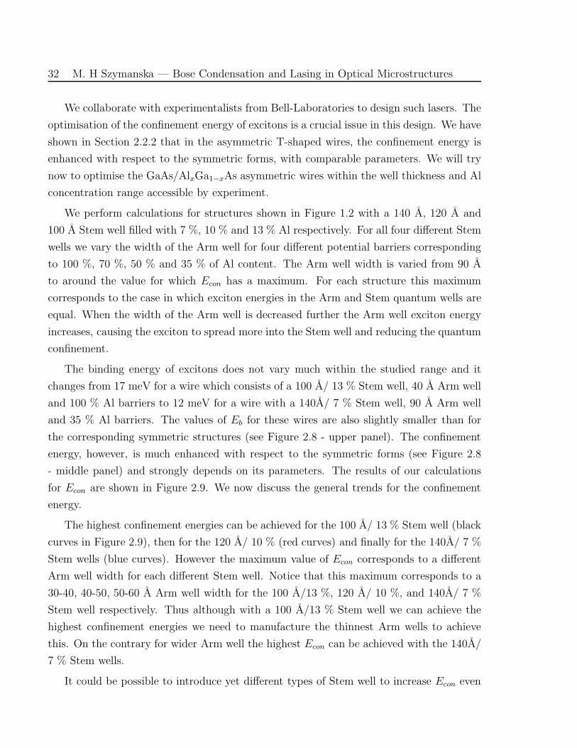
for Econ are shown in Figure 2.9. We now discuss the general trends for the confinement
energy.
The highest confinement energies can be achieved for the 100 A/ 13 % Stem well (black
curves in Figure 2.9), then for the 120 A/ 10 % (red curves) and finally for the 140A/ 7 %
Stem wells (blue curves). However the maximum value of Econ corresponds to a different
Arm well width for each different Stem well. Notice that this maximum corresponds to a
30-40, 40-50, 50-60 A Arm well width for the 100 A/13 %, 120 A/ 10 %, and 140A/ 7 %
Stem well respectively. Thus although with a 100 A/13 % Stem well we can achieve the
highest confinement energies we need to manufacture the thinnest Arm wells to achieve
this. On the contrary for wider Arm well the highest Econ can be achieved with the 140A/
7 % Stem wells.
It could be possible to introduce yet different types of Stem well to increase Econ even
2. Calculations of the electron-hole states in T-shaped quantum wires 33
30 40 50 60 70 80 90
Dx [A]
0
10
20
30
40
50
60
70
Eco
n[m
eV]
Figure 2.9: Confinement energy Econ = E2Dexc − E1Dexc for asymmetric wires as afunction of the Arm well width Dx, for different Stem wells and potential barriers. Bluecurves correspond to the 140A/ 7 % Stem well, red curves to the 120 A/ 10 % and blackcurves to the 100 A/ 13 % Stem well. Solid lines are for 100 % Al barriers, dashed linesfor 70 % Al, dotted lines for 50 % Al and dashed-dotted lines are for 35 % Al barriers.
further. Unfortunately, the higher Econ could only be achieved by using Arm wells thinner
than 30 A which would not be practical. The dependence of Econ on the Al content in
potential barriers is the simplest one. Econ always increases with an increase of Al content.
Although generally the value of the confinement energy is highest for high Al contents
and thin Arm wells both these features bring additional experimental difficulties [18]:
• For higher Al concentration, yields of cleavage in CEO become worse and interfaces
get rougher which degrades the transport properties.
• Above 50% AlGaAs becomes an indirect-gap semiconductor.
34 M. H Szymanska — Bose Condensation and Lasing in Optical Microstructures
• It becomes harder to make an optical wave guide for a laser structure with higher Al
concentration.
• Thinner Arm-QWs cause higher thresholds in lasing.
• In thinner QWs the wavefunctions tends to penetrate deeply into AlGaAs, which
may reduce the photoluminescence.
In optimising wires for practical applications one needs to take into account both the
above mentioned difficulties and the gain in the confinement energy. The detailed calcula-
tions of Econ for a wide range of structures are therefore very important. Our calculations
are being used to design quantum wire lasers which would operate at room temperature.
This work, in collaboration with Bell-Laboratories, is still in progress.
2.2.4 Accuracy of the Results
In our method the one-particle energies and wave functions are calculated first. The one-
particle energies are very well converged with respect to all the variables such as unit cell
size, number of points on the grid and the number of plane waves to an accuracy of 0.1
meV. We use on average as many as 160 000 plane waves which corresponds to 400 × 400
points on the grid (200×200 in the small unit cell). We obtain excellent agreement between
our energies for the single electron and hole and those obtained by Glutsch et al. [10]. For
the 70 A, x=0.35 symmetric quantum wire we obtain Ee = 47.09 meV and Eh = 7.47 meV
while their results are Ee = 47.2 meV and Eh = 7.5 meV. According to our calculations
there is only one electron state confined in the wire and its confinement energy E2D−1D
(i.e., the difference between well-like and wire-like electron states) is 9 meV. This is in very
good agreement with other methods. L. Pfeiffer et al. [15] using eight band ~k ·~p calculations
obtained a confinement energy of 8.5 meV for the same structure. Kiselev et al. [14] using
the so-called free-relaxation method obtained approximately the same value of 9 meV.
These one-particle wave functions are then used as a basis set for the two-particle
calculations. The E1Dexc is very well converged with respect to the number of points
on the grid (as for the one-particle calculations), and with the size of the basis set (see
Appendix A, Tables A.1 and A.2). Convergence is usually achieved with about 20×20×20
(8000) basis functions. In order to minimise finite size effects we use quite big unit cells
(from 43 times the well width, Dx for very thin wires (10 A) to 7 times Dx for the 80
A wire). The exciton energy E1Dexc is converged to within about 0.2 meV and E2Dexc to
2. Calculations of the electron-hole states in T-shaped quantum wires 35
within 0.3 meV which gives an accuracy for Eb of about 0.3 meV and for Econ of about 0.5
meV.
The other problem which can influence the accuracy of the results is the uncertainty
associated with the input parameters. The electron and hole masses as well as the dielectric
constant are standard but the potential barriers vary a lot depending on the publication.
We have found quite different values of the potential offsets for the same material interfaces
in the literature. We have examined the influence of this uncertainty on the final results
by performing calculations for the extrema of the sets of parameters found. Both binding
and confinement energies can differ by approximately 0.5 meV.
For the parameters that we are using, the results are converged to within 0.3 meV for
the binding and 0.5 meV for the confinement energies. However, one needs to remember
that these parameters are not well calibrated and this could lead to an additional error in
both energies of about 0.5 meV.
The first few (4 in the case of Fig 2.5) excited states of the wire which are below the
1Dcon and the 2Dexc are discrete, quasi-1D excitonic states and are converged to within
1 meV. Convergence of the higher states in the continuum is more complicated. Because
our system is finite we obtain only a sampling of the continuum states. When we increase
the unit cell size we automatically calculate more states within the same energy region and
they do not have a one to one correspondence with the states calculated using a smaller
unit cell. The new states appear in between the old ones, with smaller oscillator strengths
so that the total oscillator strength is conserved. When the Gaussian broadening of a 4
meV (FWHM) is added to the spectra then for a sufficiently big unit cell the broadened
spectrum is independent of the unit cell, thus convergence is reached (see Appendix A,
Figures A.1 and A.2). The spectra shown in Figs 2.2 and 2.5 are converged in the sense
that the continuum is accurately sampled on the scale of 4meV.
2.3 Conclusions
We have performed an exact diagonalisation within a finite basis set of the Hamiltonian
which describes an interacting electron-hole pair in a T-shaped quantum wire. We have
obtained the ground and excited state energies and wave functions for this system. The first
group of excited states shows an s-like excitonic character where the electron is localised
in the wire but is bound to the hole which spreads into one of the wells. Due to the fact
that the electron and hole are not localised in the same region, we have a group of low
36 M. H Szymanska — Bose Condensation and Lasing in Optical Microstructures
oscillator-strength states just above the ground state. This group is followed by a number of
states with large oscillator strength which are 2D excitonic states scattered on the T-shaped
intersection. The excitonic lasing from one of those states has been experimentally observed
[8]. We have also performed a detailed study of the exciton binding and confinement
energies as a function of the well width and Al molar fraction for symmetric and asymmetric
wires. The highest binding energy in any structure so far constructed is calculated to be
16.5 meV which is much smaller than previously thought. Our results have shown that for
optimised asymmetric wires, the confinement energy is enhanced but the binding energy
is slightly lower with respect to those in symmetric wires. For GaAs/AlxGa1−xAs wires
we have obtained an upper limit for the binding energy of around 25 meV in a 10 A
wide GaAs/AlAs structure which suggests that other materials need to be explored in
order to achieve room temperature applications. InyGa1−yAs/AlxGa1−xAs might be a
good candidate.
Chapter 3
Two-mode Excitonic Lasing in
T-shaped Quantum Wires
In this Chapter we present the experimental observation of two-mode lasing in asymmetric,
T-shaped quantum wires [8]. Under strong excitation the simultaneous lasing from two
levels in the structure is achieved. We then apply the numerical calculations described in
Chapter 2 for structures used in this experiment and identify the origin of the two laser
modes.
3.1 Experimental Set-up
The laser structure studied experimentally consists of two intersecting quantum wells fab-
ricated by cleaved edge overgrowth molecular beam epitaxy (MBE). One set of quantum
wells called Stem wells are grown on a (001) GaAs substrate, and then in a second MBE
growth an intersecting Arm quantum well is grown on the (110) crystal face exposed after
an in situ cleave of the GaAs wafer in the growth chamber (see Fig. 1.2). Previously
reported work studied a symmetric configuration in which Arm and Stem quantum wells
had the same width [6]. The work described here is in an asymmetric structure, where the
Stem well is significantly wider but filled with low percentage AlGaAs to compensate for
the reduction in confinement energy. The structure is composed of 20 Stem QWs, 140 A
wide with a 7 % Al content intersecting a single 56 A or 60 A GaAs Arm QW to form
the T-QWRs. These 20-wire structures are embedded in a multilayer arrangement that
forms an optical cavity whose fundamental mode concentrates the emitted light around
the quantum wires. A detailed description of the optical cavity can be found [6]. Along
37
38 M. H Szymanska — Bose Condensation and Lasing in Optical Microstructures
the wire axis, the 500 mm long laser cavity is limited by two additional (011) cleaved sur-
faces that are left uncoated. The carriers are resonantly excited by optically pumping the
Stem quantum well adjacent to the wire intersection. These carriers populate the Stem
wells and after phonon emission [19], they relax to wire states and eventually recombine.
The enlarged absorption length associated with the wider stem wells in this sample results
in much larger carrier generation than in previous T-wire laser devices. This manifests
itself also in a x4 reduction of laser threshold power compared with symmetric structures.
In what follows, the excitation power refers to that of the pump laser focused homoge-
neously over the whole optical wire cavity area, and a maximum pump power of 500 mW
corresponds to a density of ∼ 2kW/cm2.
3.2 Experimental Data
The effect of changes in photoexcitation intensity on lasing and also on the spontaneous
emission in these T-wire lasers is displayed in Fig. 3.1. Below threshold both the on- and
off-axis spectra show the luminescence from the excitonic ground state of the wires at 1.570
eV. The luminescence from the Arm well appears as a weak shoulder in the off-axis emission
but becomes more prominent as a second peak at 1.593 meV as the photoexcitation energy
is raised. At 140 mW the sample is lasing in multimode with the gain centred at 1.567
meV (L1), an energy which is very close to the excitonic ground state of the wire. This
photon energy is preserved for both kinds of emissions over the whole range of excitation
powers. At pump powers above 300 mW a second lasing line (L2) appears and eventually
dominates the laser emission. Simultaneous lasing at two lines in a single cavity implies a
population inversion of more than one quantum state.
The positions of both laser lines remain largely constant, and L1 stays centred at an
energy that is very close to that of the exciton at low excitation power. Given the accuracy
in the measurement of the lasing line we can state that any shift is less than the spacing
between adjacent cavity modes (0.3 meV). The observations seem to imply that laser gain
displays excitonic behaviour even at the high excitation powers.
The switching between the L1 and L2 laser lines shown in Fig. 3.1 has the striking
temperature dependence displayed in Fig. 3.2 [9]. At 40 K the sample is lasing in a well
defined single mode at 1.57 eV. In the temperature range 50 - 60 K, when the pump power
exceeds about 20 times threshold (see inset in Fig. 3.2), the drastic change in the laser
emission occurs. The system becomes bistable with emergence of the second line (L2), blue
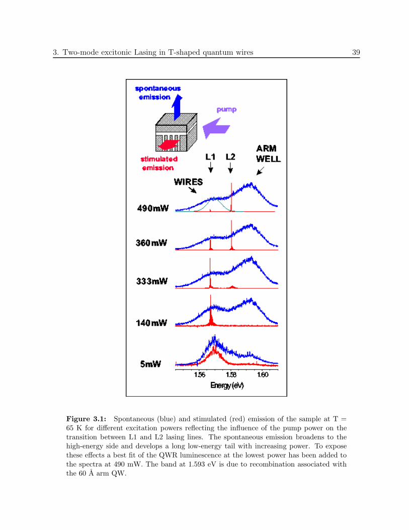
3. Two-mode excitonic Lasing in T-shaped quantum wires 39
Figure 3.1: Spontaneous (blue) and stimulated (red) emission of the sample at T =65 K for different excitation powers reflecting the influence of the pump power on thetransition between L1 and L2 lasing lines. The spontaneous emission broadens to thehigh-energy side and develops a long low-energy tail with increasing power. To exposethese effects a best fit of the QWR luminescence at the lowest power has been added tothe spectra at 490 mW. The band at 1.593 eV is due to recombination associated withthe 60 A arm QW.
40 M. H Szymanska — Bose Condensation and Lasing in Optical Microstructures
shifted 14 meV from the fundamental line (L1). Raising the temperature further causes
the intensity of L1 to quickly diminish and the single mode lasing from the L2 lines is
obtained. After the L2 line is established the threshold power begins to rapidly increase
with temperature, causing the emission to decay into a multimode operation that persists
to 80 K.
It has to be stressed that with increasing temperature the L1 line disappears, but with
increasing pump power it saturates (when L2 turns on) and then slowly diminishes in
absolute intensity.
Figure 3.3 presents the normalised difference of the two integrated intensities and shows
that switching abruptly takes place within an interval ∆T ≈ 5K around 55 K. At tem-
peratures above 55 K the intensity of L2 increases monotonically with pump power, while
L1 starts to diminish once both intensities become comparable. With the onset of L2 an
increase up to 33 % in the slope can be measured as a kink in the response curve, in com-
parison with the gain saturation observed at lower temperatures where L2 is absent (see
inset in Fig 3.3). These characteristics are suggestive of a phase transition, where carriers
and photons are involved. A system of two lasing modes, represented by two coupled os-
cillators, has a rich phase diagram which will be expected to influence its photon statistics
properties [20].
In the Figure 3.3 b the excitation spectra of both lasing modes are depicted for two
temperatures. At temperatures below the transition (50 K), when only L1 is active, the
excitation spectrum reproduces the expected absorption of the Stem well. But when both
lasing lines are present, their intensities are strongly coupled as evidenced by the excitation
spectrum at 57 K. Once L2 is activated, it competes with L1 to the point that the excitation
spectrum of L1 develops a dip where L2 is maximum.
While the L1 line clearly corresponds to the excitonic ground state of the wires the
origin of the L2 mode is not obvious. Since the binding energy of the exciton in this geom-
etry is approximately 14 meV, one possibility might be exciton dissociation into itinerant
quantum wire states. To distinguish possible scenarios another T-wire laser was studied
with narrower Arm QW of 56 A, which should have a nearly identical exciton binding
energy, but a different energy level structure. In this sample a substantially higher L1 - L2
splitting of 17 meV was observed (see Fig. 3.4). The 20 % increased shift is not consistent
with that exciton breakup hypothesis.
Since the L2 transition is only observed at high excitation levels the first suggestion was
that L2 has entirely a many-body origin, connected with the presence of an electron-hole
3. Two-mode excitonic Lasing in T-shaped quantum wires 41
plasma in the system. Such persistence of excitonic effects in 1D to high carrier density
would be very remarkable.
Another possibility would be that the second lasing mode (L2) corresponds to a higher
excitonic state in the structure.
Sorting out these possibilities represents a renewed challenge as there is no independent
determination of the density. Both scenario suggest that an upper limit for the density is
approximately 1 per Bohr radius and thus is roughly of the order that one would expect
for the transition from e-h plasma to bound excitons.
We have performed calculations which suggest that the L2 line corresponds to a higher
excitonic state in the structure. We have first developed a rate equation model for the
two-mode laser, presented in Chapter 4, assuming that the laser action takes place for two
exciton-like states. This model can qualitatively reproduce the experimental data provided
that the oscillator strength times the density of states for the upper excitonic state (L2
line) is higher than that for the ground state (L1 line). Motivated by this result we have
performed detailed calculations for both structures studied in the experiment (56 A and
60 A Arm QWs) to identify the excitonic states which correspond to the two laser modes.
3.3 Calculations
We have performed numerical calculations of a single electron-hole pair in the T-shaped
geometries of the two experiments to explore how the geometric changes might affect the
spontaneous luminescence. To this end, we performed (see Chapter 2 and reference [21])
exact diagonalisations to determine not only the ground but also the excited states of the
excitonic system, with results shown in Fig 3.5. The results for the two cases are similar:
the ground state 1D exciton is bound 14 meV below the one-dimensional particle-hole
continuum, and confined by 22 (26) meV in comparison to the 2D exciton in a 60 (56)
A arm well. There is an absolute shift of 3.5 meV in the 1D-exciton energy between the
two structures, in agreement with experiment. We also find several excited states of the
bound 1D exciton. States above the edge marking the free particle-hole excitation of the
wire are of course in a continuum, and the discrete spectrum above 65 (69) meV is due
to the finite box size of our calculations. We note that there is a broad peak of oscillator
strength lying slightly above the 2D quantum well energy. Inspection of the wavefunctions
of the large oscillator-strength states reveals that they are principally quasi-2D-exciton-like
states strongly perturbed by the quantum wire potential, resonant with (and thus decaying
42 M. H Szymanska — Bose Condensation and Lasing in Optical Microstructures
into) the continuum states of the wire. The oscillator strength of the 1D-continuum states
themselves is weaker.
While these calculations are valid only for low density, the absence of substantial shifts
in the luminescence spectrum with pumping suggests that the calculations can be used as
a guide to the assignment of the transitions. L2 lies near but below the energy marking
the onset of 2D excitons in the Arm well. Nevertheless, the shift of L2 from 14 to 17
meV between the 60 and 56 A structures mirrors the calculated change of the exciton
confinement energy in the wire from 22 to 26 meV, indicating that L2 may have well-like
character.
Since the L2 transition is only observed at high excitation levels, it is possible that the
8-9 meV shift of the L2 line from the calculated 2D exciton edge may be a redshift induced
by screening by the occupied 1D excitons.
Very recent experiments [22] give an additional support for the hypothesis that the
L2 line is associated with the well excitons in the vicinity of the wires. With a reduction
of a number of wires in the sample the threshold power for L1 lasing goes up while the
threshold for L2 remains constant.
3.4 Conclusions
We have presented the experimental observation of two-mode lasing in asymmetric, T-
shaped quantum wires [8]. Under strong excitation the simultaneous lasing from two
levels in the structure was achieved. We have applied the numerical calculations described
in Chapter 2 for both structures, with 60 A and 56 A Arm quantum well, used in this
experiment to identify the origin of the two laser modes.
We have obtained an absolute shift of 3.5 meV in the 1D-exciton energy between the
two structures, in agreement with experiment. We have also found several excited bound
1D exciton states but there is no evidence for emission from these states. Shift of L2
from 14 to 17 meV between the 60 and 56 A structures mirrors the calculated change of
the exciton confinement energy in the wire from 22 to 26 meV, suggesting that L2 has a
well-like character, though the position of L2 is somewhat below the onset of 2D excitons
in the arm well. Early suggestions that L2 is associated with emission from 1D e-h plasma
are not substantiated.
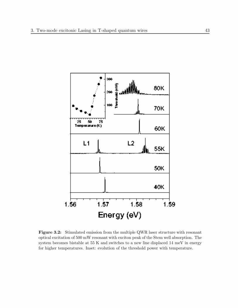
3. Two-mode excitonic Lasing in T-shaped quantum wires 43
Figure 3.2: Stimulated emission from the multiple QWR laser structure with resonantoptical excitation of 500 mW resonant with exciton peak of the Stem well absorption. Thesystem becomes bistable at 55 K and switches to a new line displaced 14 meV in energyfor higher temperatures. Inset: evolution of the threshold power with temperature.
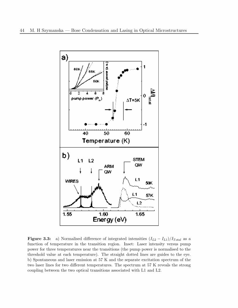
44 M. H Szymanska — Bose Condensation and Lasing in Optical Microstructures
Figure 3.3: a) Normalised difference of integrated intensities (IL2 − IL1)/ITotal as afunction of temperature in the transition region. Inset: Laser intensity versus pumppower for three temperatures near the transitions (the pump power is normalised to thethreshold value at each temperature). The straight dotted lines are guides to the eye.b) Spontaneous and laser emission at 57 K and the separate excitation spectrum of thetwo laser lines for two different temperatures. The spectrum at 57 K reveals the strongcoupling between the two optical transitions associated with L1 and L2.
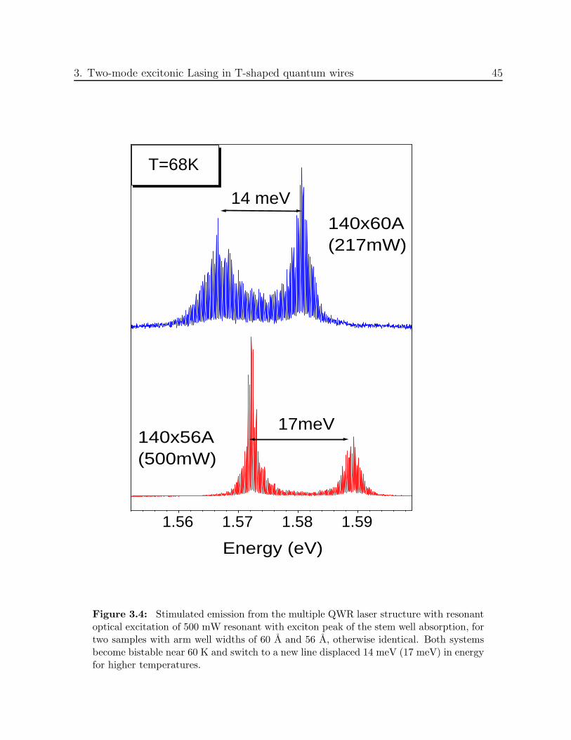
3. Two-mode excitonic Lasing in T-shaped quantum wires 45
1.56 1.57 1.58 1.59
140x56A (500mW)
14 meV
17meV
T=68K
Energy (eV)
140x60A (217mW)
Figure 3.4: Stimulated emission from the multiple QWR laser structure with resonantoptical excitation of 500 mW resonant with exciton peak of the stem well absorption, fortwo samples with arm well widths of 60 A and 56 A, otherwise identical. Both systemsbecome bistable near 60 K and switch to a new line displaced 14 meV (17 meV) in energyfor higher temperatures.
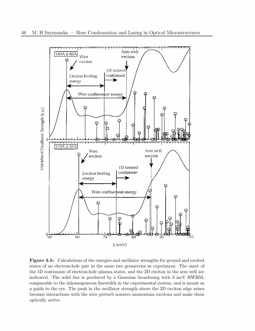
46 M. H Szymanska — Bose Condensation and Lasing in Optical Microstructures
Figure 3.5: Calculations of the energies and oscillator strengths for ground and excitedstates of an electron-hole pair in the same two geometries as experiment. The onset ofthe 1D continuum of electron-hole plasma states, and the 2D exciton in the arm well areindicated. The solid line is produced by a Gaussian broadening with 3 meV HWHM,comparable to the inhomogeneous linewidth in the experimental system, and is meant asa guide to the eye. The peak in the oscillator strength above the 2D exciton edge arisesbecause interactions with the wire perturb nonzero momentum excitons and make themoptically active.
Chapter 4
Rate Equation Model for a
Two-Mode Laser
In this Chapter we develop a rate equation model for a two-mode laser. Assuming that
the laser action takes place for two different exciton-like states, we can reproduce the same
qualitative behaviour of the laser, as observed in the experiment described in Chapter 3.
The results of this Section support the hypothesis that the second lasing mode (L2) is
associated with the higher excitonic state in the structure. The calculations of the spectra
for experimentally studied wires (see Chapter 3) suggested that this higher excitonic state
has a well-like character.
4.1 Experimental Motivations
In Chapter 3 we have described in detail the experimental observation of a two-mode lasing
in asymmetric, T-shaped quantum wires. The first lasing mode comes from the ground
state exciton while the nature of the second lasing line is not known. Determination of the
origin of this line represents a renewed challenge as there is no independent determination of
the density which might be very high, of the order that one would expect for the transition
from e-h plasma to bound excitons. Thus many-body effects might be important.
The laser shows very interesting behaviour which might help to determine the origin
of the second lasing mode. There is a switching between the two laser modes as the
temperature or the pump power is changed. At low pump powers and low temperatures
only the first laser line (L1) is present. There is a quite wide range of pump intensities
and a very narrow range of temperatures for which the laser works in multimode in which
47
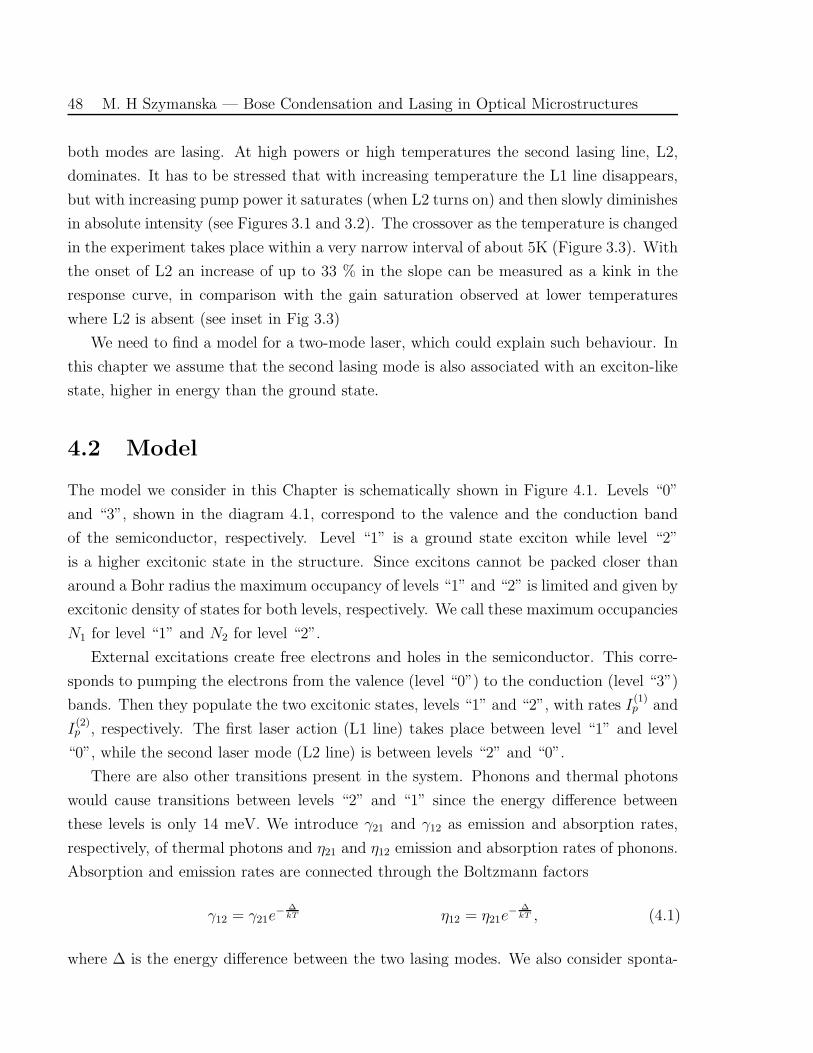
48 M. H Szymanska — Bose Condensation and Lasing in Optical Microstructures
both modes are lasing. At high powers or high temperatures the second lasing line, L2,
dominates. It has to be stressed that with increasing temperature the L1 line disappears,
but with increasing pump power it saturates (when L2 turns on) and then slowly diminishes
in absolute intensity (see Figures 3.1 and 3.2). The crossover as the temperature is changed
in the experiment takes place within a very narrow interval of about 5K (Figure 3.3). With
the onset of L2 an increase of up to 33 % in the slope can be measured as a kink in the
response curve, in comparison with the gain saturation observed at lower temperatures
where L2 is absent (see inset in Fig 3.3)
We need to find a model for a two-mode laser, which could explain such behaviour. In
this chapter we assume that the second lasing mode is also associated with an exciton-like
state, higher in energy than the ground state.
4.2 Model
The model we consider in this Chapter is schematically shown in Figure 4.1. Levels “0”
and “3”, shown in the diagram 4.1, correspond to the valence and the conduction band
of the semiconductor, respectively. Level “1” is a ground state exciton while level “2”
is a higher excitonic state in the structure. Since excitons cannot be packed closer than
around a Bohr radius the maximum occupancy of levels “1” and “2” is limited and given by
excitonic density of states for both levels, respectively. We call these maximum occupancies
N1 for level “1” and N2 for level “2”.
External excitations create free electrons and holes in the semiconductor. This corre-
sponds to pumping the electrons from the valence (level “0”) to the conduction (level “3”)
bands. Then they populate the two excitonic states, levels “1” and “2”, with rates I(1)p and
I(2)p , respectively. The first laser action (L1 line) takes place between level “1” and level
“0”, while the second laser mode (L2 line) is between levels “2” and “0”.
There are also other transitions present in the system. Phonons and thermal photons
would cause transitions between levels “2” and “1” since the energy difference between
these levels is only 14 meV. We introduce γ21 and γ12 as emission and absorption rates,
respectively, of thermal photons and η21 and η12 emission and absorption rates of phonons.
Absorption and emission rates are connected through the Boltzmann factors
γ12 = γ21e−
∆kT η12 = η21e
−∆kT , (4.1)
where ∆ is the energy difference between the two lasing modes. We also consider sponta-
4. Rate Equation Model for a Two-Mode Laser 49
3
laser mode 2 laser mode 1 γ20 γ10
η12 γ21 γ12η21
Ip2
Ip1
0
1
2
Figure 4.1: Sketch of the model for a two-mode laser system. Various levels and thetransitions between them are shown. Bold solid lines correspond to laser actions, dashedlines correspond to photon spontaneous emission and absorption while dotted-dashedlines correspond to phonon emission and absorption.
neous emissions of photons to modes different from the two lasing modes for both lasing
levels with rates γ20 and γ10, respectively.
This model combines two standard rate equations models for the semiconductor laser
and for the atomic laser. The levels “0” and “3” are alike in the semiconductor model
where the maximum occupancy of the levels are not imposed while levels “1” and “2” are
the same as in atomic lasers characterised by the parameters N1 and N2 which involve
saturation of the levels.
Without detailed calculations we can see that raising the temperature thermally depop-
ulates level “1” into level “2”. A strong pumping also increases the population of level “2”
50 M. H Szymanska — Bose Condensation and Lasing in Optical Microstructures
over level “1”, provided the trapping from level “2” into level “1” is relatively inefficient in
comparison to the rate of emission from level “2”, and provided also that the population
of level “1” can saturate.
Introducing the abbreviation r21 = γ21 + η21 and using equation (4.1) we obtain, from
a detailed balance, the rate equation for the population of the higher excitonic state (level
“2”), n2
dn2
dt= Ip(2)(N2 − n2) − r21n2(N1 − n1) + r21e
−∆kT n1(N2 − n2)
− γ20n2 − n2(1 + S2)g2 + (N2 − n2)S2g2. (4.2)
The first term in equation (4.2) corresponds to the pumping of level “2” and is proportional
to the pump power and the difference between the maximum number of excitons, N2, and
the current number of excitons in this state, n2. The second term, which describes transi-
tions from level “2” to level “1”, caused by phonons or thermal photons is proportional to
the number of excitons in level “2” and to the difference between the maximum number
of excitons in level “1”, N1, and the current number of excitons in this state, n1. Similarly
the third term describes the transitions from level “1” to level “2 ”, caused by phonon or
thermal photons. The fourth term corresponds to the spontaneous emission of photons to
modes other than the lasing modes. Finally, the fifth term describes a stimulated emission
of photons to the L2 lasing line and is proportional to the number of excitons in level “2”,
n2, and to the factor 1+S2, where S2 is a number of photons in the L2 mode. The sixth
term gives the stimulated absorption of photons from the L2 lasing mode.
Similarly, the rate equation for the number of excitons in the ground state (level “1”),
n1 is
dn1
dt= Ip(1)(N1 − n1) + r21n2(N1 − n1) − r21e
−∆kT n1(N2 − n2)
− γ10n1 − n1(1 + S1)g1 + (N1 − n1)S1g1, (4.3)
where S1 is the number of photons in the L1 lasing mode.
The rate equation for the photon number in the L1 mode is
dS2
dt= −κ2S2 + (n2 − (N2 − n2))S2g2, (4.4)
4. Rate Equation Model for a Two-Mode Laser 51
while in the L2 mode is
dS1
dt= −κ1S1 + (n1 − (N1 − n1))S1g1, (4.5)
where κ1 and κ2 are the cavity decay rates for the L1 and the L2 lasing mode, respectively.
4.3 Steady State Behaviour
We are now interested in a steady state behaviour of these four coupled equations (4.2) -
(4.5). We need to consider four different regimes:
1. S1 > 0 and S2 > 0, both modes are lasing.
2. S1 > 0 and S2 = 0, 1st mode is lasing, 2nd is not lasing.
3. S1 = 0 and S2 > 0, 1st mode is not lasing, 2nd is lasing.
4. S1 = 0 and S2 = 0, both modes are not lasing.
Experimentally all four regimes were observed in the same structure for different tem-
peratures and pump powers (see Chapter 3). It can be shown that, to have all four regimes
in the same structure in our model, the laser parameters have to satisfy the following three
conditions
A =N1
2− κ1
2g1> 0 (4.6)
C =N2
2− κ2
2g2
> 0 (4.7)
N2g2
κ2
>N1g1
κ1
. (4.8)
If we assume that the cavity decay rates for both laser modes are the same κ1 = κ2, the
condition (4.8) means that the oscillator strength times the density of states for level “2”
has to be larger than that of level “1”. It is very unlikely that the oscillator strength for any
higher excitonic state would be larger than that of the ground state, but it is very probable
that the density of states would be larger for the higher state and thus the condition would
be satisfied.
In the Chapter 3 we argued that the second lasing line is connected with quasi-2D-
52 M. H Szymanska — Bose Condensation and Lasing in Optical Microstructures
exciton-like states strongly perturbed by the quantum wire potential, resonant with (and
thus decaying into) the continuum states of the wire. The density of such states would be
much bigger than that of the ground state excitons (see Figure 3.5).
Let us now consider in more detail the four different regimes as the temperature and
pump power are changed.
• Multimode operation of the laser: S1 > 0 and S2 > 0. Using equations (4.2) - (4.5)
we can calculate the intensities of both laser lines in a steady state, assuming that
both photon modes are occupied. Introducing abbreviations
B =N1
2+
κ1
2g1, (4.9)
and
D =N2
2+
κ2
2g2, (4.10)
the intensities of the modes will be
S2 =r21κ2
(BCe−∆kT − AD + C
Ip(2)
γ21− γ20 + g2
γ21D), (4.11)
S1 =r21κ1
(−BCe− ∆kT + AD + A
Ip(1)
γ21− γ10 + g1
γ21B). (4.12)
Notice that the first two terms in equation (4.11), out of which only the first one is
temperature dependent in the whole equation, have the same magnitude but opposite
sign to the analogous terms in equation (4.12). These terms cause the competition
between the two modes as the temperature is changed. At low temperatures the first
two terms in equation (4.11) would be negative, and when the pumping (the third
term) is too low to compensate them and the losses described by the fourth term,
the L2 line will not be present. Similarly, from equation (4.12) we can see that at
high temperatures the L1 line will not be present. As the temperature is changed,
the rate equation model predicts the same switching of modes, as was experimentally
observed (see Chapter 3).
• At low temperatures and pumping rates, when S1 > 0 and S2 = 0, the intensity of
4. Rate Equation Model for a Two-Mode Laser 53
the L1 lasing line will be
S1 =AIp(1) − B(γ10 + g1)
κ1+N2
κ1∗ AIp(2) − B(γ20 + g2)e
−∆kT
A+Be−∆kT + Ip(2)
γ21+ γ20+g2
γ21
(4.13)
• At high temperatures or pump powers, when S1 = 0 and S2 > 0, the intensity of the
L2 line would be
1
κ2∗ (CIp(2) − (γ20 + g2)D +
CIp(1)e−∆kT
Ce−∆kT +D + Ip(1)
γ21+ γ10+g1
γ21
. (4.14)
Equations (4.11) - (4.14) have quite complicated forms, therefore it will be easier to
study the behaviour of the system by plotting the results for particular parameters. We
developed this model before the detailed calculations of spectra, described in Chapter 3,
were obtained and thus not all values of input parameters were available. We noticed,
however, that the qualitative behaviour of the system is not that sensitive to the input
parameters, provided that the conditions (4.6) - (4.8) are satisfied. We choose the input
parameters so that the temperature transition region is the same as in the experiment. For
different, but yet realistic, parameters the qualitative behaviour would remain the same,
but the transition temperature would change.
The most important parameter which determines the thermal coupling of the two modes
is ∆. We use exactly the same value of 14 meV for ∆ as in the experiment. The exact
values of other parameters are very difficult to determine. In this work we use approximate
values, but realistic ones for these types of structures. We normalise the parameters so
that the gains g1 = g2 = 1, N2/N1 = 100, κ1/g = κ2/g = 8.81, r21/γ20 = r21/γ10 = 10. We
choose I(1)p to be 0, which is a physical assumption, because the exciton has to get into the
well first before it can get into the wire.
In Figure 4.2 we present a phase diagram for our system. The four different phases
are marked in Fig 4.2. The phase diagram recovers the experimental behaviour, shown in
Figures 3.1 and 3.2. Let us first discuss the behaviour of the system at a fixed temperature,
lower than 59K. At very low pump powers there is no lasing in the system. With the
increase in the pump power the L1 laser mode appears first. When the pump power
is increased further, the L2 laser action starts and the system lases in multimode. The
intensity of the L1 line saturates when the L2 mode appears, while the intensity of the
L2 increases with the pump power (see Figure 4.4). Thus the L1 line slowly diminishes
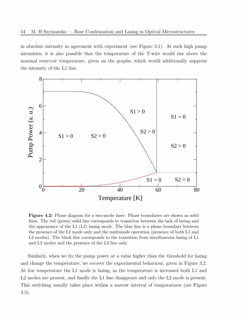
54 M. H Szymanska — Bose Condensation and Lasing in Optical Microstructures
in absolute intensity in agreement with experiment (see Figure 3.1). At such high pump
intensities, it is also possible that the temperature of the T-wire would rise above the
nominal reservoir temperature, given on the graphs, which would additionally suppress
the intensity of the L1 line.
0 20 40 60 80
Temperature [K]
0
2
4
6
8
Pum
p P
ower
(a.
u.)
S1 = 0 S2 = 0
S1 > 0 S2 = 0
S1 > 0
S2 > 0
S1 = 0
S2 > 0
Figure 4.2: Phase diagram for a two-mode laser. Phase boundaries are shown as solidlines. The red (green) solid line corresponds to transition between the lack of lasing andthe appearance of the L1 (L2) lasing mode. The blue line is a phase boundary betweenthe presence of the L1 mode only and the multimode operation (presence of both L1 andL2 modes). The black line corresponds to the transition from simultaneous lasing of L1and L2 modes and the presence of the L2 line only.
Similarly, when we fix the pump power at a value higher than the threshold for lasing
and change the temperature, we recover the experimental behaviour, given in Figure 3.2.
At low temperature the L1 mode is lasing, as the temperature is increased both L1 and
L2 modes are present, and finally the L1 line disappears and only the L2 mode is present.
This switching usually takes place within a narrow interval of temperatures (see Figure
4.3).
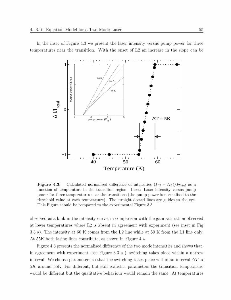
4. Rate Equation Model for a Two-Mode Laser 55
In the inset of Figure 4.3 we present the laser intensity versus pump power for three
temperatures near the transition. With the onset of L2 an increase in the slope can be
40 50 60
Temperature (K)
−1
0
1
∆ I/I
tota
l
∆T = 5K0 2 4 6pump power (P
th )
outp
ut p
ower
(a.
u.)
50 K
60 K55 K
Figure 4.3: Calculated normalised difference of intensities (IL2 − IL1)/ITotal as afunction of temperature in the transition region. Inset: Laser intensity versus pumppower for three temperatures near the transitions (the pump power is normalised to thethreshold value at each temperature). The straight dotted lines are guides to the eye.This Figure should be compared to the experimental Figure 3.3
observed as a kink in the intensity curve, in comparison with the gain saturation observed
at lower temperatures where L2 is absent in agreement with experiment (see inset in Fig
3.3 a). The intensity at 60 K comes from the L2 line while at 50 K from the L1 line only.
At 55K both lasing lines contribute, as shown in Figure 4.4.
Figure 4.3 presents the normalised difference of the two mode intensities and shows that,
in agreement with experiment (see Figure 3.3 a ), switching takes place within a narrow
interval. We choose parameters so that the switching takes place within an interval ∆T ≈5K around 55K. For different, but still realistic, parameters the transition temperature
would be different but the qualitative behaviour would remain the same. At temperatures
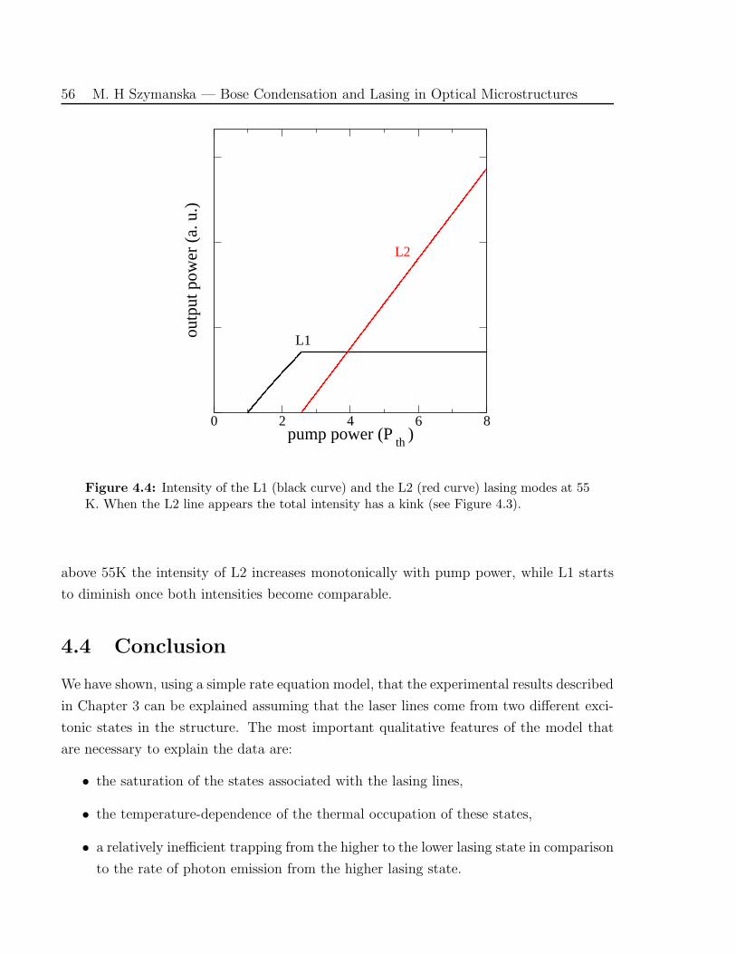
56 M. H Szymanska — Bose Condensation and Lasing in Optical Microstructures
0 2 4 6 8pump power (P
th )
outp
ut p
ower
(a.
u.)
L1
L2
Figure 4.4: Intensity of the L1 (black curve) and the L2 (red curve) lasing modes at 55K. When the L2 line appears the total intensity has a kink (see Figure 4.3).
above 55K the intensity of L2 increases monotonically with pump power, while L1 starts
to diminish once both intensities become comparable.
4.4 Conclusion
We have shown, using a simple rate equation model, that the experimental results described
in Chapter 3 can be explained assuming that the laser lines come from two different exci-
tonic states in the structure. The most important qualitative features of the model that
are necessary to explain the data are:
• the saturation of the states associated with the lasing lines,
• the temperature-dependence of the thermal occupation of these states,
• a relatively inefficient trapping from the higher to the lower lasing state in comparison
to the rate of photon emission from the higher lasing state.
4. Rate Equation Model for a Two-Mode Laser 57
Using this model we have recovered:
• the switching between the two modes as temperature is changed,
• the saturation of the L1 line as the pump power is increased,
• the region of a multimode operation,
• experimentally observed behaviour of intensities of the two lasing lines.
This very good qualitative agreement between the model and the experiment suggests
that we indeed have lasing from two different excitonic states in the structure. Motivated by
this agreement we performed detailed calculations, presented in the Chapter 3, to identify
the L2 excitonic state.

Chapter 5
Summary and Future Directions
5.1 Summary
In this work we have developed a method to calculate electron-hole states in quantum wires.
We have included the single-particle potential and the Coulomb interaction between the
electron and hole on an equal footing, and have performed exact diagonalisation of the two-
particle problem within a finite basis set. We have calculated energies, oscillator strengths
for radiative recombination, and two-particle wave functions for the ground state exciton
and around 100 excited states in a T-shaped wire.
We have studied in detail the shape of the wave functions to gain insight into the nature
of the various states for selected symmetric and asymmetric wires in which laser emission
has been experimentally observed. We have found
• That the first group of excited states shows an s-like excitonic character where the
electron is localised in the wire but is bound to the hole which spreads into one of
the wells. Due to the fact that the electron and hole are not localised in the same
region, we have a group of low oscillator-strength states just above the ground state.
• That the group of low oscillator-strength states is followed by a number of states
with large oscillator strength which are 2D excitonic states scattered on the T-shaped
intersection.
We have also performed a detailed study of the exciton binding and confinement energies
as a function of the well width and Al molar fraction for symmetric and asymmetric wires.
We have shown
59
60 M. H Szymanska — Bose Condensation and Lasing in Optical Microstructures
• That the highest binding energy in any structure so far constructed is calculated to
be 16.5 meV which is much smaller than previously thought.
• That for optimised asymmetric wires, the confinement energy is enhanced but the
binding energy is slightly lower with respect to those in symmetric wires.
• That for GaAs/AlxGa1−xAs wires we have obtained an upper limit for the binding
energy of around 25 meV in a 10 A wide GaAs/AlAs structure which suggests that
other materials need to be explored in order to achieve room temperature applica-
tions. InyGa1−yAs/AlxGa1−xAs might be a good candidate.
Our calculations are being used to design improved excitonic lasers which will oper-
ate at room temperature. In particular we have studied in detail the GaAs/AlxGa1−xAs
structures in order to optimise the confinement energy of the wire.
We have described an experimental observation of an interesting phenomenon of a
two-mode lasing in asymmetric T-shaped wires. We have then
• Developed a rate equation model for a two-mode laser. Assuming that the laser
action takes place for two different exciton-like states, we can reproduce the same
qualitative behaviour of the laser, as observed in the experiment.
• Applied the detailed numerical calculations for structures used in this experiment
and identified the origin of the two laser modes. The first lasing line comes from the
ground state exciton while the second line is most probably associated with quasi-
2D-exciton-like states strongly perturbed by the quantum wire potential
5.2 Future Directions
• Our calculations are being used to design quantum wire lasers which would operate
at room temperature. This work, in collaboration with Bell-Laboratories, is still in
progress and detailed calculations for structures with different materials or shapes
might be useful.
• It would be of interest to perform the rate equation calculations for the exact param-
eters of the structures used in the experiment.
• More complex extensions could consider doped quantum wires or including a finite
concentration of electron-hole pairs in the wire.
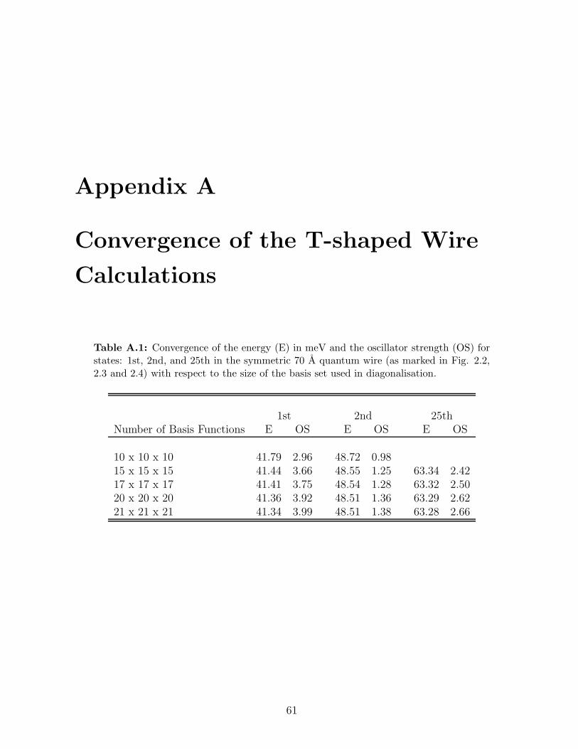
Appendix A
Convergence of the T-shaped Wire
Calculations
Table A.1: Convergence of the energy (E) in meV and the oscillator strength (OS) forstates: 1st, 2nd, and 25th in the symmetric 70 A quantum wire (as marked in Fig. 2.2,2.3 and 2.4) with respect to the size of the basis set used in diagonalisation.
1st 2nd 25thNumber of Basis Functions E OS E OS E OS
10 x 10 x 10 41.79 2.96 48.72 0.9815 x 15 x 15 41.44 3.66 48.55 1.25 63.34 2.4217 x 17 x 17 41.41 3.75 48.54 1.28 63.32 2.5020 x 20 x 20 41.36 3.92 48.51 1.36 63.29 2.6221 x 21 x 21 41.34 3.99 48.51 1.38 63.28 2.66
61
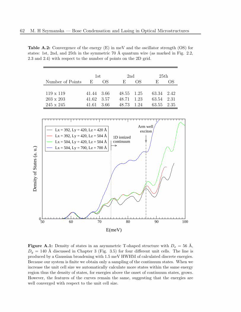
62 M. H Szymanska — Bose Condensation and Lasing in Optical Microstructures
Table A.2: Convergence of the energy (E) in meV and the oscillator strength (OS) forstates: 1st, 2nd, and 25th in the symmetric 70 A quantum wire (as marked in Fig. 2.2,2.3 and 2.4) with respect to the number of points on the 2D grid.
1st 2nd 25thNumber of Points E OS E OS E OS
119 x 119 41.44 3.66 48.55 1.25 63.34 2.42203 x 203 41.62 3.57 48.71 1.23 63.54 2.31245 x 245 41.61 3.66 48.73 1.24 63.55 2.35
50 60 70 80 90 100
E(meV)
0
Den
sity
of S
tate
s (a
. u.)
Lx = 392, Ly = 420, Lz = 420 Å
Lx = 392, Ly = 420, Lz = 504 Å
Lx = 504, Ly = 420, Lz = 504 Å
Lx = 504, Ly = 700, Lz = 700 Å
Arm well exciton
1D ionizedcontinuum
Figure A.1: Density of states in an asymmetric T-shaped structure with Dx = 56 A,Dy = 140 A discussed in Chapter 3 (Fig. 3.5) for four different unit cells. The line isproduced by a Gaussian broadening with 1.5 meV HWHM of calculated discrete energies.Because our system is finite we obtain only a sampling of the continuum states. When weincrease the unit cell size we automatically calculate more states within the same energyregion thus the density of states, for energies above the onset of continuum states, grows.However, the features of the curves remain the same, suggesting that the energies arewell converged with respect to the unit cell size.
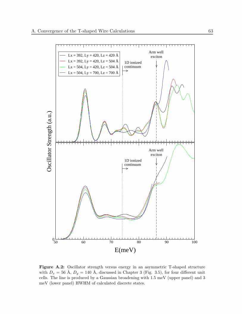
A. Convergence of the T-shaped Wire Calculations 63
Lx = 392, Ly = 420, Lz = 420 Å
Lx = 392, Ly = 420, Lz = 504 Å
Lx = 504, Ly = 420, Lz = 504 Å
Lx = 504, Ly = 700, Lz = 700 Å
Arm well exciton
1D ionizedcontinuum
50 60 70 80 90 100
E(meV)
0
Arm well exciton
1D ionizedcontinuum
Osc
illat
or S
tren
gth
(a.u
.)
Figure A.2: Oscillator strength versus energy in an asymmetric T-shaped structurewith Dx = 56 A, Dy = 140 A, discussed in Chapter 3 (Fig. 3.5), for four different unitcells. The line is produced by a Gaussian broadening with 1.5 meV (upper panel) and 3meV (lower panel) HWHM of calculated discrete states.

Appendix B
Comments on the Effective Mass
Approximation
Calculations of the T-shaped wire states are performed using the effective mass approxi-
mation with an anisotropic hole mass. In the effective mass approximation electron and
heavy hall single parabolic bands are assumed. This approximation is justified in the
energy region of interest.
In Figure B.1 (upper panel) we present the hole band structure along the wire direction,
taken from [23], for sample S2 (see Table 2.1) experimentally studied in [3], which consist
of 53 A Stem and 48 A Arm quantum wells with AlAs barriers. For the same sample, in
Figure B.1 (lower panel), we present the contribution from different kz states in a ground
and a first excited state wavefunction given by equation (2.2).∑
i,j |ci,j,kz|2 is plotted as
a function of kz. Notice, that the hole bands are parabolic for kz up to around 0.013
A−1. The contribution from kz higher than 0.013 A−1 is negligible for presented first two
states. The higher states are more spatially extended than the first two states and thus
they will decay in the kz space even faster than the presented two states. The conduction
band is shown to be parabolic for kz up to 0.04 A−1 for AlAs barriers [24]. For lower Al
concentration the conduction band is parabolic even for higher kz up to 0.11 A−1 for Al
concentration, x=0.3, while the spatial extension of states would be larger, and thus the
region in k-space smaller than in the AlAs case. Thus the parabolic band effective mass
approximation is justified for all structures being considered in this work.
Another issue is that the second hole band in Figure B.1 (upper panel), although
parabolic in the energy region of interest, splits into two branches with different, by around
factor of two, effective masses. The binding energies are, however, not that sensitive to the
65
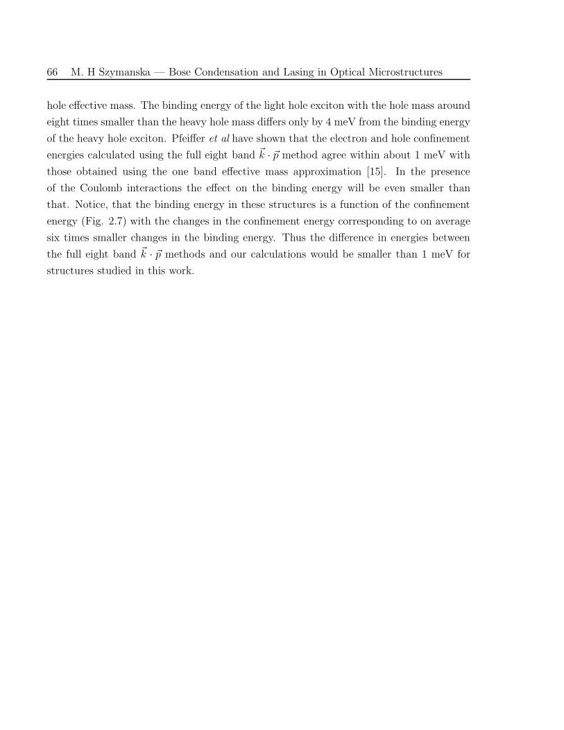
66 M. H Szymanska — Bose Condensation and Lasing in Optical Microstructures
hole effective mass. The binding energy of the light hole exciton with the hole mass around
eight times smaller than the heavy hole mass differs only by 4 meV from the binding energy
of the heavy hole exciton. Pfeiffer et al have shown that the electron and hole confinement
energies calculated using the full eight band ~k · ~p method agree within about 1 meV with
those obtained using the one band effective mass approximation [15]. In the presence
of the Coulomb interactions the effect on the binding energy will be even smaller than
that. Notice, that the binding energy in these structures is a function of the confinement
energy (Fig. 2.7) with the changes in the confinement energy corresponding to on average
six times smaller changes in the binding energy. Thus the difference in energies between
the full eight band ~k · ~p methods and our calculations would be smaller than 1 meV for
structures studied in this work.
B. Comments on the Effective Mass Approximation 67
Figure B.1: Upper panel: Hole band structure along the z axis of the T-QWR. The fullcircles identify the states that are quasi-one-dimensional wire-like states or resonances.Dashed lines show the lowest-hole subbands of the isolated Arm and Stem quantumwells. Taken from [23]. Lower panel: Coefficient of the basis set expansion in k-spaceas a function of k in the z direction in the present calculations using the effective massapproximation.

Bibliography
[1] Y. C. Chang, L. L. Chang, and L. Esaki, Appl. Phys. Lett. 47, 1324 (1985).
[2] H. Akiyama, T. Someya, M. Yoshita, T. Sasaki, and H. Sakaki, Phys. Rev. B 57,
3765 (1998).
[3] T. Someya, H. Akiyama, and H. Sakaki, Phys. Rev. Lett. 76, 2965 (1996).
[4] H. Gislason, W. Langbein, and J. M. Hvam, Superlattices and Microstruct. 22, 217
(1997).
[5] W. Langbein, H. Gislason, and J. M. Hvam, Phys. Rev. B 54, 14595 (1996).
[6] W. Wegscheider, L. N. Pfeiffer, M. M. Dignam, A. Pinczuk, K. W. West, S. L.
McCall, and R. Hull, Phys. Rev. Lett. 71, 4071 (1993).
[7] J. Hasen, L. N. Pfeiffer, A. Pinczuk, S. He, K. W. West, and Brian S. Dennis, Nature
390, 54 (1997).
[8] J. Rubio, L. N. Pfeiffer, M. H. Szymanska, A. Pinczuk, S. He, H. U. Baranger, P. B.
Littlewood, K. W. West, and B. S. Dennis, unpublished.
[9] J. Rubio, L. N. Pfeiffer, M. H. Szymanska, A. Pinczuk, S. He, H. U. Baranger, P. B.
Littlewood, K. W. West, and B. S. Dennis, unpublished.
[10] S. Glutsch, F. Bechstedt, W. Wegscheider, and G. Schedelbeck, Phys. Rev. B 56,
4108 (1997).
[11] F. Rossi, G. Goldoni, and E. Molinari, Phys. Rev. Lett. 78, 3527 (1997).
[12] D. Brinkman and G. Fishman, Phys. Rev. B 56, 15211 (1997).
69
70 M. H Szymanska — Bose Condensation and Lasing in Optical Microstructures
[13] G. W. Bryant, P. S. Julienne, and Y. B. Band, Superlattices and Microstruct. 20(4),
601 (1996).
[14] A. A. Kiselev and U. Rossler, Semicond. Sci. Technol. 11, 203 (1996).
[15] L. Pfeiffer, H. Baranger, D. Gershoni, K. Smith, and W Wegscheider, in K. Eberl et
al. (eds.), Low Dimensional Structures prepared by Epitaxial Growth or Regrowth on
Patterned Substrates, 93-100, 1995 Kluwer Academic Publishers.
[16] M. C. Payne, M. P. Teter, D. C. Allan, T. A. Arias, and J. D. Joannopoulos, Reviews
of Modern Physics 64, 1045 (1992).
[17] T. Kato, Communications on Pure and Applied Mathematics 10, 151 (1957).
[18] H. Akiyama, pravite communications
[19] G. A. Narvaez., et al. Physica E 2, 983 (1998).
[20] G. S. Agarwal and S. Dattagupte Phys. Rev. A 26, 880-887 (1982).
[21] M. H. Szymanska, P. B. Littlewood, and R. J. Needs, Phys. Rev. B 63, 205317 (2001).
[22] L. Pfeiffer, pravite communications
[23] G. Goldoni, F. Rossi, E. Molinari, A. Fasolino, Phys. Rev. B 55, 7110 (1997).
[24] S. Pescetelli, A. Di Carlo, and P. Lugli, Phys. Rev. B 56, R1668 (1997).