bipolar resistance switching in pt/cuox/pt via local electrochemical reduction
TRANSCRIPT

Bipolar resistance switching in Pt/CuOx/Pt via local electrochemical reductionKenneth D'Aquila, Charudatta Phatak, Martin V. Holt, Benjamin D. Stripe, Sheng Tong, Woon Ik Park,
Seungbum Hong, and Amanda K. Petford-Long
Citation: Applied Physics Letters 104, 242902 (2014); doi: 10.1063/1.4883398 View online: http://dx.doi.org/10.1063/1.4883398 View Table of Contents: http://scitation.aip.org/content/aip/journal/apl/104/24?ver=pdfcov Published by the AIP Publishing Articles you may be interested in Anomalous effect due to oxygen vacancy accumulation below the electrode in bipolar resistance switchingPt/Nb:SrTiO3 cells APL Mat. 2, 066103 (2014); 10.1063/1.4884215 Impact of Joule heating on the microstructure of nanoscale TiO2 resistive switching devices J. Appl. Phys. 113, 163703 (2013); 10.1063/1.4803033 Local heating-induced plastic deformation in resistive switching devices J. Appl. Phys. 110, 054514 (2011); 10.1063/1.3633271 Nonvolatile bipolar resistive switching in Au/BiFeO3/Pt J. Appl. Phys. 109, 124117 (2011); 10.1063/1.3601113 Investigation of the electroforming process in resistively switching TiO 2 nanocrosspoint junctions Appl. Phys. Lett. 96, 122902 (2010); 10.1063/1.3367752
This article is copyrighted as indicated in the article. Reuse of AIP content is subject to the terms at: http://scitation.aip.org/termsconditions. Downloaded to IP:
146.137.70.70 On: Mon, 23 Jun 2014 22:03:41

Bipolar resistance switching in Pt/CuOx/Pt via localelectrochemical reduction
Kenneth D’Aquila,1,2 Charudatta Phatak,1 Martin V. Holt,3 Benjamin D. Stripe,3
Sheng Tong,3 Woon Ik Park,1 Seungbum Hong,1,a) and Amanda K. Petford-Long1,2
1Materials Science Division, Argonne National Laboratory, Lemont, Illinois 60439, USA2Department of Materials Science and Engineering, Northwestern University, Evanston, Illinois 60208, USA3Nanoscience and Technology Division, Argonne National Laboratory, Lemont, Illinois 60439, USA
(Received 23 April 2014; accepted 1 June 2014; published online 17 June 2014)
The local changes in copper oxidation state and the corresponding resistance changes in Pt/CuOx/Pt
nanoscale heterostructures have been investigated using x-ray nanoprobe spectro-microscopy and
current-voltage characterization. After gentle electroforming, during which the current-voltage
behavior remains non-linear, the low resistance state was reached, and we observed regions of 160 nm
width that show an increase in Cu K-alpha fluorescence intensity, indicative of partial reduction of the
CuOx. Analysis of the current voltage curves showed that the dominant conduction mechanism is
Schottky emission and that the resistance state is correlated with the Schottky barrier height. We
propose that the reversible resistivity change in these Pt/CuOx/Pt heterostructures occurs through local
electrochemical reduction leading to change of the Schottky barrier height at the interface between Pt
and the reduced CuOx layers and to change of the CuOx resistivity within laterally confined portions
of the CuOx layer. These experiments reveal important insights into the mechanism of resistance
switching of Pt/CuOx/Pt performed in a current and voltage regime that does not create a metallic
conduction path. VC 2014 AIP Publishing LLC. [http://dx.doi.org/10.1063/1.4883398]
Resistance switching in metal/insulator/metal hetero-
structures is a process by which an applied electric field
reversibly changes the electrical resistance across the oxide
between two or more states.1–4 Many research groups have
explored the physical origins of this phenomenon and have
constructed resistance change based memory devices or bio-
inspired artificial neuron devices.5,6 There have also been a
wide range of proposed mechanisms. These can be classified
as being primarily electronic, ionic, or thermal in origin.7
These mechanisms can result in the formation of a conduct-
ing bridge phase, a change in the energy barrier at the metal/
insulator interface, or both.6
Heterostructures containing copper oxide have shown
repeatable resistance switching and typically involve a high
resistance state (HRS) that is two or three orders of magni-
tude larger than the low resistance state (LRS).8
Additionally, the LRS typically displays Ohmic conduction
while a variety of leakage current mechanisms have been
proposed for the HRS.9 Considerable progress has been
made in identifying the chemical changes that result from
the resistance switching process within Pt/CuOx/Pt hetero-
structures. Drift of oxygen vacancies through the CuOx layer
plays an important role, and the contribution of oxygen
vacancies have been explored using in-situ transmission
electron microscopy (TEM) analysis and photoemission
electron microscopy (PEEM).10,11 These studies proposed
that the LRS results from the formation of conductive
copper-rich CuOx (a mixture of Cu and Cu2O) bridge
regions.10,11 After switching back to the HRS, re-oxidized
CuOx regions were found near the metal electrode.15
The resistance switching mechanism for Pt/CuOx/Pt het-
erostructures described above differs from the electrochemi-
cal metallization mechanism proposed for Cu metal
electrode-based systems, such as Cu/SiO2/Ir, Cu/Ta2O5/Pt,
and Cu/Ge0.4Se0.6, in which Cu cations are the primary mo-
bile ions due the abundant supply of un-oxidized Cu in the
electrode layer.12–14 Resistance switching in these materials
occurs via three steps: (1) Electrochemical dissolution of Cu
atom to Cu cation at the anode/oxide interface, (2) electric
field-driven drift of Cu cation through the oxide layer, and
(3) reduction of Cu cation to Cu atom.15,16 For the
Pt/CuOx/Pt system studied here, although both Cu and O
vacancies in CuOx could migrate in a strong electric field,
previous reports suggest that oxygen vacancies are the pri-
mary mobile defects.11,17
The goal of our study is to explore the mechanisms by
which resistance switching occurs in a current regime before
metallic conduction paths are fully formed. We have
explored this question by studying the resistance switching
mechanisms of Pt/CuOx/Pt heterostructures. Changes to the
Cu oxidation state were observed using hard x-ray nanoprobe
fluorescence microscopy and were correlated with the room
temperature charge transport behavior. Our study could pro-
vide insights for device applications because multi-order of
magnitude resistance switching, in which regions of oxide
are fully reduced to metal, can involve mechanical damage
to the top electrode and high local temperatures that cause
unwanted thermal diffusion.18,19
The samples analyzed in these experiments consisted of
SiN/Ti/Pt/40 nm CuOx/Pt. Reactive RF magnetron sputtering
was used to deposit the oxide layer from a Cu target, result-
ing in oxygen-deficient CuO that we will refer to as CuOx.
The top Pt electrodes were 2 lm in diameter, and we refer to
a)Author to whom correspondence should be addressed. Electronic mail:
0003-6951/2014/104(24)/242902/5/$30.00 VC 2014 AIP Publishing LLC104, 242902-1
APPLIED PHYSICS LETTERS 104, 242902 (2014)
This article is copyrighted as indicated in the article. Reuse of AIP content is subject to the terms at: http://scitation.aip.org/termsconditions. Downloaded to IP:
146.137.70.70 On: Mon, 23 Jun 2014 22:03:41

the region of the sample under the top electrode as the ‘pad’.
The x-ray nanoprobe fluorescence microscopy and
spectro-microscopy experiments were performed at the
Advanced Photon Source Sector 26-ID in the Center for
Nanoscale Materials, Argonne National Laboratory. A
Fresnel zone plate was used to achieve a spatial resolution of
80 nm. Beam energies in a range from 8969 eV to 8999 eV
were used to measure the fluorescence intensity of the Cu
K-alpha peak at each scan point. Conducting-atomic force
microscopy (C-AFM) was used for electrical probing in
order to prevent damage to the thin SiN membranes. For all
current-voltage measurements, the bottom electrode was
grounded and the tip was biased. The SET operation, per-
formed at negative bias, switches a pad from the HRS to the
LRS. The RESET operation, performed at positive bias,
switches a pad from the LRS back to the HRS (See the sup-
plementary material20 for more experiment details).
Figure 1 shows bipolar current-voltage curves for two
SiN/Ti/Pt/CuOx/Pt heterostructures: (a) Pad 1 and (b) Pad 2.
In both cases, the curves show a repeatable bipolar resistance
switching process with clear hysteresis. Despite the difference
in compliance current (600 lA for Pad 1 and 900 lA for Pad
2) the shapes of the I–V curves are very similar, with an asym-
metry between the positive voltage (RESET) curve and the
negative voltage (SET) curve. The resistance ratio
(RHRS/RLRS) was calculated at a voltage of 0.5 V for each het-
erostructure, giving values of 2.8 for Pad 1 and 4.8 for Pad 2.
In order to explore possible changes to the Cu oxidation
state between the LRS and HRS, single energy x-ray fluores-
cence maps were collected on three different SiN/Ti/Pt/
CuOx/Pt heterostructures as shown in Figures 2(a)–2(c). Pad
0 was scanned in its as-prepared state. Transport measure-
ments made on other heterostructures shows that the
as-prepared pads are in the HRS. After several resistance
switching cycles, Pad 1 was scanned in the LRS, and Pad 2
was scanned in the HRS. The fluorescence maps were nor-
malized so that the scan points in the off-pad region for each
map have the same average intensity. The active heterostruc-
ture region can be observed from the reduction in intensity
of the Cu K-alpha signal, which results from the presence of
the top Pt electrode. The exact position of the top electrode
edge was determined from the Pt fluorescence map and is
indicated on each map by the dotted outline. We are confin-
ing our analysis to a sub-region modified by the applied elec-
tric field, indicated on each map with a solid outline. We
excluded the regions near the pad edges to exclude variations
that can result from edge roughness or changes in thickness.
We can assume that the variation in Cu K-alpha intensity
across the pad region (area under the top electrode) shows a
normal distribution if the composition of the CuOx layer and
the thickness of the Pt top electrode are relatively homogene-
ous. In order to look for regions that show statistically distinct
Cu fluorescence intensity, the distribution of Cu fluorescence
intensity was plotted for each of the three pads using a normal
probability plot as shown in Figs. 2(d)–2(f). For Pad 0 (as-
prepared, HRS) and Pad 2 (HRS after RESET), 99.8% of the
points follow a linear trend line in the probability plot, which
indicates that the Cu fluorescence data are well described by a
normal distribution. For Pad 1, which is in the LRS, 98% of
the points in the probability plot follow a linear trend, but
there are 2% of points at the extremes of the distribution with
fluorescence intensity that is noticeably higher than would be
expected for a normal distribution.
The magnitude of the residual between the measured in-
tensity and the statistically-modeled intensity (straight line
shown on each normal probability plot) can thus be used to
identify the location of scan points at which the Cu K-alpha
fluorescence intensity is statistically greater than the
expected distribution, as shown in Figs. 2(g)–2(i). Pad 1
(LRS), shows several clusters of scan points with high Cu in-
tensity and with a cluster size from 150 to 200 nm. However,
Pads 0 and 2 (HRS), show relatively few scan points with
high Cu intensity. Thus, there is a clear correlation between
local regions with high Cu intensity and a low resistance
state for the Pt/CuOx/Pt heterostructure.
In order to explore in more detail the possible variations
in stoichiometry of the CuOx for the higher fluorescence inten-
sity regions in the LRS, we performed x-ray fluorescence
spectro-microscopy on the lower left corner of Pad 1. The
resulting set of Cu K-alpha fluorescence maps obtained at a
series of incident energies can also be thought of as a 2D map
of Cu K-alpha fluorescence spectra. Fig. 3(a) shows an exam-
ple of a Cu K-alpha fluorescence spectrum from a single scan
point, together with the pad-averaged spectrum and vertical
lines indicating the 63r distribution width at each energy.
Each value in the pad-averaged spectrum was obtained by
averaging over all scan points within the selected region under
the top Pt electrode at a particular incident energy.
An average percent difference map, as shown in
Fig. 3(b), was created to identify locations across the pad at
which the Cu K-alpha peak has higher intensity than the pad-
averaged peak. The values in Fig. 3(b) were computed
according to the following equation:
Davg x; yð Þ ¼1
n
X8999
E¼8969
IEðx; yÞ � IpadE
IPadE
� 100; (1)
where IE is the fluorescence intensity at photon energy E and
position (x,y) and IpadE is the fluorescence intensity at photon
energy E averaged over the region shown in Fig. 3(b) that is
under the Pt electrode. The sum is over the incident photon
energy values used (n¼ 21, in steps of 1.5 eV). The red/
orange regions shown in Fig. 3(b) indicate scan points at
which the local Cu K-alpha fluorescence peak has higher in-
tensity than the pad-averaged peak. As can be seen, a single
160 nm size region, indicated by the arrow, is observed at
which the intensity is >4.4% higher than the pad average.FIG. 1. I–V curves for (a) Pad 1 (b) Pad 2. After gradual electroforming,
both pads repeatedly switch between high and low resistance states.
242902-2 D’Aquila et al. Appl. Phys. Lett. 104, 242902 (2014)
This article is copyrighted as indicated in the article. Reuse of AIP content is subject to the terms at: http://scitation.aip.org/termsconditions. Downloaded to IP:
146.137.70.70 On: Mon, 23 Jun 2014 22:03:41

The x-ray spectro-microscopy results confirm that regions
of higher Cu K-alpha fluorescence intensity in the single
energy maps shown in Fig. 2 also show higher Cu K-alpha
across the entire peak edge. Several x-ray absorption studies in
the literature have shown that x-ray absorption across the Cu
K-edge increases as CuO is reduced to Cu2O and to Cu.21–23
Although the detailed shape of our Cu K-alpha fluorescence
edge is not identical to those seen using x-ray absorption, we
assume that this trend applies qualitatively within this range of
incident photon energy.24 As a result, we can conclude that
within the spots of higher Cu K-alpha fluorescence intensity,
the CuOx has been partially reduced to CuOy where 1> x> y.
FIG. 2. (a)–(c) Cu K-alpha fluorescence maps, (d)–(f) normal probability plots of Cu K-alpha fluorescence counts, and (g)–(i) maps of difference between
measured Cu fluorescence counts at each point and the counts modeled by a normal distribution for (a), (d), and (g) HRS as-prepared, (b), (e), and (h) LRS after
SET, (c), (f), and (i) HRS after RESET (a)–(c).
FIG. 3. X-ray nanoprobe spectro-microscopy: (a) a Cu K-alpha fluorescence spectra and (b) map of the average percent differences of Cu K-alpha fluorescence
intensity as defined above. These data were collected from the bottom left corner of Pad 1.
242902-3 D’Aquila et al. Appl. Phys. Lett. 104, 242902 (2014)
This article is copyrighted as indicated in the article. Reuse of AIP content is subject to the terms at: http://scitation.aip.org/termsconditions. Downloaded to IP:
146.137.70.70 On: Mon, 23 Jun 2014 22:03:41
In order to better explain the correlation between electri-
cal resistance state and the presence of reduced CuOx, we
first assume that the LRS consists of a CuOx matrix and
CuOy conductive bridges (1> x> y). The total resistance
Rtot is modeled in Eq. (2) in terms of a bridge resistance Rb
and a matrix resistance Rm connected in parallel. In the
HRS, Rtot equals Rm, whereas in the LRS, Rtot is<Rm by a
factor f, which is defined as the total resistance ratio
(RHRS/RLRS).
Rtot ¼RbRm
Rb þ Rm¼ 1
f
� �Rm: (2)
We assume that current flows homogeneously through
the bridge and matrix of thickness t and area Ab and Am
respectively. The areas were measured from the x-ray
microscopy data and the thickness from a cross-section
transmission electron microscopy image shown in Fig. S2.
Thus Rb and Rm in Eq. (2) can be substituted by qb and qm
and the appropriate values of t, Ab, and Am. The oxide resis-
tivity ratio (matrix/bridge, qm/qb) can now be found by solv-
ing Eq. (2) with these substitutions
qm
qb
¼ ðf � 1ÞAm
Ab: (3)
We can use Eq. (3) to estimate the oxide resistivity ratio
and infer the extent of the CuOx reduction in the LRS
bridges. Assuming that conductive bridges occupy only 2%
of the pad area (Ab/Am¼ 0.02), the observed factor of four
decrease in the pad resistance can be accounted for if the
conductive bridges oxide, CuOy has a resistivity that is a fac-
tor of 150 less than that of the matrix. According to the liter-
ature, the resistivity of Cu2O and CuO can each vary over
three orders of magnitude. Cu2O has the highest maximum
resistivity, followed by CuO and then Cu metal.25 However,
it was also shown that the resistivity of oxygen-depleted
CuO is an order of magnitude higher than that of
oxygen-rich Cu2O.25,26 These results agree with our oxide
resistivity ratio estimate, suggesting that we have indeed
stayed within a regime where we are changing the oxidation
state of the Cu oxide without reducing it to Cu metal.
Although a local reduction of CuOx creates regions
(bridges) of lower resistivity, our I-V curves show that the
LRS is not metallic. In order to determine the conduction
mechanism for both states, the current-voltage data were
plotted in a way that displays a linear trend line if the gov-
erning equation for a particular conduction mechanism is
obeyed. The conduction mechanisms tested were Schottky,
Frenkel-Poole emission, space-charge limited current, and
Fowler-Nordheim tunneling. The best agreement with the
data was for Schottky emission, whose governing equation is
the modified Richardson equation given by27
J ¼ AGT2e
� DE�ffiffiffiffie3F4pe
p� �kT : (4)
Here, J is the current density, T is the absolute temperature,
DE is effective Schottky barrier height, F is the electric field,
and e is the dielectric constant.
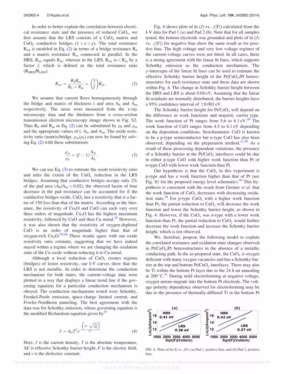
Fig. 4 shows plots of ln (J) vs. �(jFj) calculated from the
I-V data for Pad 1 (a) and Pad 2 (b). Note that for all samples
tested, the bottom electrode was grounded and plots of ln (J)
vs. �(jFj) for negative bias show the same result as for posi-
tive bias. The high voltage and very low voltage regimes of
the current-voltage curves were not fitted. In all cases, there
is a strong agreement with the linear fit lines, which supports
Schottky emission as the conduction mechanism. The
y-intercepts of the linear fit lines can be used to estimate the
effective Schottky barrier height of the Pt/CuOx/Pt hetero-
structures for each resistance state and these data are shown
within Fig. 4. The change in Schottky barrier height between
the HRS and LRS is about 0.04 eV. Assuming that the linear
fit residuals are normally distributed, the barrier heights have
a 95% confidence interval of 60.001 eV.
The Schottky barrier height for Pt/CuOx will depend on
the difference in work functions and majority carrier type.
The work function of Pt ranges from 5.6 to 6.1 eV.28 The
work function of CuO ranges from 4.5 to 6.1 eV depending
on the deposition conditions. Stoichiometric CuO is known
to be a p-type semiconductor but n-type CuO has also been
observed, depending on the preparation method.11,29 As a
result of these processing dependent variations, the presence
of a Schottky barrier at the Pt/CuOx interfaces could be due
to either p-type CuO with higher work function than Pt or
n-type CuO with lower work function than Pt.
Our hypothesis is that the CuOx in this experiment is
p-type and has a work function higher than that of Pt (see
Fig. S1 for the proposed energy level schematic).10 This hy-
pothesis is consistent with the result from Greiner et al. that
the work function of CuOx decreases with decreasing oxida-
tion state.24 For p-type CuOx with a higher work function
than Pt, the partial reduction to CuOy will decrease the work
function and lower the Schottky barrier height, as shown in
Fig. 4. However, if the CuOx was n-type with a lower work
function than Pt, the partial reduction to CuOy would further
decrease the work function and increase the Schottky barrier
height, which is not observed.
We, therefore, propose the following model to explain
the correlated resistance and oxidation state changes observed
in Pt/CuOx/Pt heterostructures in the absence of a metallic
conducting path. In the as-prepared state, the CuOx is oxygen
deficient with many oxygen vacancies and has a Schottky bar-
rier at the top and bottom Pt/CuOx interfaces. There may also
be Ti within the bottom Pt layer due to the 24 h air annealing
at 200 �C.31 During mild electroforming at negative voltage,
oxygen anions migrate into the bottom Pt electrode. The volt-
age polarity dependence observed for electroforming may be
due to the presence of thermally-diffused Ti in the bottom Pt
FIG. 4. Plots of ln (J) vs �(F): (a) Pad 1, positive bias, and (b) Pad 2, positive
bias.
242902-4 D’Aquila et al. Appl. Phys. Lett. 104, 242902 (2014)
This article is copyrighted as indicated in the article. Reuse of AIP content is subject to the terms at: http://scitation.aip.org/termsconditions. Downloaded to IP:
146.137.70.70 On: Mon, 23 Jun 2014 22:03:41

electrode which gives it a greater capacity to absorb oxygen
than the top electrode. Regions in which oxygen migration
has occurred become partially reduced, and this lowers the
CuOx work function.30 As a result, the Schottky barrier height
becomes lower, and the LRS is achieved. Under positive volt-
age, the oxygen anions migrate from the bottom electrode
back into the CuOy, and the HRS is achieved once the origi-
nal Schottky barrier height is restored.
We believe that this mechanism of resistance switching
in Pt/CuOx/Pt heterostructures is an early stage of the
redox-based resistance switching previously reported, in
which a metallic conduction path is formed.10 Our study
demonstrates the role of the Schottky barrier at the Pt/CuOx
interfaces on the resistance switching process in the absence
of a metallic conduction path, and we propose that perform-
ing resistance switching in this regime could lead to more
reliable switching behavior for resistance-change based
memory devices or bio-inspired artificial neuron devices.
In conclusion, we showed that there is a partial reduc-
tion of the as-prepared CuOx when changing from HRS to
LRS. Our results show that the dominant conduction mecha-
nism is Schottky emission and that the effective barrier
height scales with the resistance state of the heterostructure.
Our model for resistance switching in Pt/CuOx/Pt hetero-
structures in the absence of a metallic conducting path is
based on the electric field driven migration of oxygen anions
that electrochemically reduce/oxidize the CuOx. This leads
to modulation of both the local CuOx resistivity and the
effective Schottky barrier height.
The work was supported by the U.S. Department of
Energy, Office of Science, Materials Sciences and
Engineering Division. We acknowledge use of the Center for
Nanoscale Materials, a U.S. Department of Energy, Office of
Science, Office of Basic Energy Sciences User Facility under
Contract No. DE-AC02-06CH11357. We acknowledge C.
Alvarez, Y. Liu, Y.-Y. Choi, S. Zhang, and A. Roelofs at
Argonne National Laboratory for their support in x-ray
nanoprobe experiment.
1S. Seo, M. J. Lee, D. H. Seo, E. J. Jeoung, D.-S. Suh, Y. S. Joung, I. K.
Yoo, I. R. Hwang, S. H. Kim, I. S. Byun, J.-S. Kim, J. S. Choi, and B. H.
Park, Appl. Phys. Lett. 85, 5655 (2004).2D.-H. Kwon, K. M. Kim, J. H. Jang, J. M. Jeon, M. H. Lee, G. H. Kim,
X.-S. Li, G.-S. Park, B. Lee, S. Han, M. Kim, and C. S. Hwang, Nat.
Nanotechnol. 5, 148 (2010).3O. Heinonen, M. Siegert, A. Roelofs, A. K. Petford-Long, M. Holt, K.
d’Aquila, and W. Li, Appl. Phys. Lett. 96, 103103 (2010).
4S. H. Chang, J. Kim, C. Phatak, K. D’Aquila, S. K. Kim, J. Kim, S. J.
Song, C. S. Hwang, J. A. Eastman, J. W. Freeland, and S. Hong, ACS
Nano 8, 1584 (2014).5S. H. Jo, T. Chang, I. Ebong, B. B. Bhadviya, P. Mazumder, and W. Lu,
Nano Lett. 10, 1297 (2010).6R. Waser and M. Aono, Nat. Mater. 6, 833 (2007).7J. J. Yang, D. B. Strukov, and D. R. Stewart, Nat. Nanotechnol. 8, 13
(2013).8P. Zhou, H. B. Lv, M. Yin, L. Tang, Y. L. Song, T. A. Tang, Y. Y. Lin, A.
Bao, A. Wu, S. Cai, H. Wu, C. Liang, and M. H. Chi, J. Vac. Sci.
Technol., B 26, 1030 (2008).9R. Dong, D. S. Lee, W. F. Xiang, S. J. Oh, D. J. Seong, S. H. Heo, H. J.
Choi, M. J. Kwon, S. N. Seo, M. B. Pyun, M. Hasan, and H. Hwang, Appl.
Phys. Lett. 90, 042107 (2007).10R. Yasuhara, K. Fujiwara, K. Horiba, H. Kumigashira, M. Kotsugi, M.
Oshima, and H. Takagi, Appl. Phys. Lett. 95, 012110 (2009).11S.-J. Choi, G.-S. Park, K.-H. Kim, W.-Y. Yang, H.-J. Bae, K.-J. Lee, H.
Lee, S. Y. Park, S. Heo, H.-J. Shin, S. Lee, and S. Cho, J. Appl. Phys. 110,
056106 (2011).12T. Tsuruoka, K. Terabe, T. Hasegawa, and M. Aono, Nanotechnology 21,
425205 (2010).13S. Z. Rahaman, S. Maikap, H.-C. Chiu, C.-H. Lin, T.-Y. Wu, Y.-S. Chen,
P.-J. Tzeng, F. Chen, M.-J. Kao, and M.-J. Tsai, Electrochem. Solid-State
Lett. 13, H159 (2010).14C. Schindler, M. Weides, M. N. Kozicki, and R. Waser, Appl. Phys. Lett.
92, 122910 (2008).15I. Valov, R. Waser, J. R. Jameson, and M. N. Kozicki, Nanotechnology
22, 254003 (2011).16A. Prakash, D. Jana, and S. Maikap, Nanoscale Res. Lett. 8, 418 (2013).17R. Waser, R. Dittmann, G. Staikov, and K. Szot, Adv. Mater. 21, 2632
(2009).18J. P. Strachan, D. B. Strukov, J. Borghetti, J. J. Yang, G. Medeiros-
Ribeiro, and R. S. Williams, Nanotechnology 22, 254015 (2011).19J. J. Yang, F. Miao, M. D. Pickett, D. A. A. Ohlberg, D. R. Stewart, C. N.
Lau, and R. S. Williams, Nanotechnology 20, 215201 (2009).20See supplementary material at http://dx.doi.org/10.1063/1.4883398 for
details on the experimental procedures (n.d.).21X. Wang, J. C. Hanson, A. I. Frenkel, J.-Y. Kim, and J. A. Rodriguez,
J. Phys. Chem. B 108, 13667 (2004).22J. Y. Kim, J. A. Rodriguez, J. C. Hanson, A. I. Frenkel, and P. L. Lee,
J. Am. Chem. Soc. 125, 10684 (2003).23A. Gaur, B. D. Shrivastava, and S. K. Joshi, J. Phys. Conf. Ser. 190,
012084 (2009).24R. Kurian, K. Kunnus, P. Wernet, S. M. Butorin, P. Glatzel, and F. M. F.
de Groot, J. Phys. Condens. Matter 24, 452201 (2012).25V. F. Drobny and L. Pulfrey, Thin Solid Films 61, 89 (1979).26L. De Los Santos Valladares, D. H. Salinas, A. B. Dominguez, D. A.
Najarro, S. I. Khondaker, T. Mitrelias, C. H. W. Barnes, J. A. Aguiar, and
Y. Majima, Thin Solid Films 520, 6368 (2012).27M. E. Kiziroglou, X. Li, A. A. Zhukov, P. A. J. de Groot, and C. H. de
Groot, Solid State Electron. 52, 1032 (2008).28F. Gossenberger, T. Roman, K. Forster-Tonigold, and A. Groß, Beilstein J.
Nanotechnol. 5, 152 (2014).29W. Siripala and J. Jayakody, Sol. Energy Mater. 14, 23 (1986).30M. T. Greiner, L. Chai, M. G. Helander, W.-M. Tang, and Z.-H. Lu, Adv.
Funct. Mater. 22, 4557 (2012).31J. J. Yang, J. P. Strachan, Q. Xia, D. A. A. Ohlberg, P. J. Kuekes, R. D.
Kelley, W. F. Stickle, D. R. Stewart, G. Medeiros-Ribeiro, and R. S.
Williams, Adv. Mater. 22, 4034 (2010).
242902-5 D’Aquila et al. Appl. Phys. Lett. 104, 242902 (2014)
This article is copyrighted as indicated in the article. Reuse of AIP content is subject to the terms at: http://scitation.aip.org/termsconditions. Downloaded to IP:
146.137.70.70 On: Mon, 23 Jun 2014 22:03:41