automatización de máquina de torrefacción de café para el
TRANSCRIPT
AUTOMATIZACIÓN DE MÁQUINA DE TORREFACCIÓN DE CAFÉ PARA EL
LABORATORIO DEL PROGRAMA DE INGENIERÍA AGRÍCOLA DE LA
UNIVERSIDAD SURCOLOMBIANA
ANGÉLICA MARÍA CÁRDENAS CASTAÑO
JENIFER TATIANA OSORIO GUZMÁN
UNIVERSIDAD SURCOLOMBIANA FACULTAD DE INGENIERÍA
PROGRAMA DE INGENIERÍA ELECTRÓNICA NEIVA – HUILA
2012
AUTOMATIZACIÓN DE MÁQUINA DE TORREFACCIÓN DE CAFÉ PARA EL
LABORATORIO DEL PROGRAMA DE INGENIERÍA AGRÌCOLA DE LA
UNIVERSIDAD SURCOLOMBIANA
ANGÉLICA MARÍA CÁRDENAS CASTAÑO JENIFER TATIANA OSORIO GUZMÁN
Proyecto de grado presentado como requisito para optar al título de Ingeniero Electrónico
Director AGUSTIN SOTO OTÁLORA
Docente Programa Ingeniería Electrónica
Codirector JOSÉ DUBAN HENAO CUÉLLAR
Docente Programa Ingeniería Agrícola
UNIVERSIDAD SURCOLOMBIANA FACULTAD DE INGENIERÍA
PROGRAMA DE INGENIERÍA ELECTRÓNICA NEIVA – HUILA
2012
Nota de aceptación:
___________________________________________ ___________________________________________ ___________________________________________ ___________________________________________ ___________________________________________ ___________________________________________ ___________________________________________
___________________________________________ Firma del director del proyecto
___________________________________________ Firma del primer jurado
___________________________________________ Firma del segundo jurado
Neiva, __ de Noviembre de 2012
A Dios por el don de la vida;
A mis padres Gloria y Darío, pues han sido mi mayor inspiración y mi mejor
ejemplo de perseverancia y constancia;
A mis hermanas Jessica, Angie y Tatiana, quienes han sido mi apoyo constante;
A mis familiares y amigos, por creer en mí.
ANGÉLICA MARÍA CÁRDENAS CASTAÑO
A mi Dios, por darme tantas oportunidades;
A mis padres Miriam y Evelio por todo su amor y confianza en mí;
A mis hermanos Wilmer, Paula y Felipe por ser mi inspiración;
A Gloria y a Darío, mis segundos padres,
Por su apoyo incondicional todos estos años;
A Jessica, Angie y Angélica por brindarme su cariño y hermandad;
A mis familiares y amigos por tantos momentos vividos.
JENIFER TATIANA OSORIO GUZMÁN.

AGRADECIMIENTOS
Los autores expresan su agradecimiento a:
Nuestra Alma Mater la Universidad Surcolombiana, por brindarnos la oportunidad
de realizar nuestros estudios profesionales.
Ing. Agustín Soto, Director de trabajo de grado, por su apoyo, guía y amistad.
Ing. Duván Henao, Co-Director de trabajo de grado, por brindarnos su apoyo
además de las herramientas para la elaboración de este trabajo.
Nuestros profesores Ing. Edilberto Polanía, Ing. Diego Jiménez, Ing. Germán
Martínez, Ing. Ramiro Perdomo, Ing. Neisar Salazar, Ing. Vladimir Mosquera, Ing.
Carlos Pérez, Ing. Faiber Robayo, Ing. Jesús Salgado, Ing. Julián Molina, Ing.
Javier Rubio; por brindarnos sus conocimientos y su valioso tiempo.
Nuestros amigos por su compañía y colaboración durante nuestro proceso de
realización profesional; especialmente a Junior Francisco Quijano por su total
apoyo y gran amistad.
Encargados de los laboratorios por brindarnos siempre las mejores condiciones de
trabajo.
Todas las personas que directa o indirectamente colaboraron en la realización de
este proyecto de grado
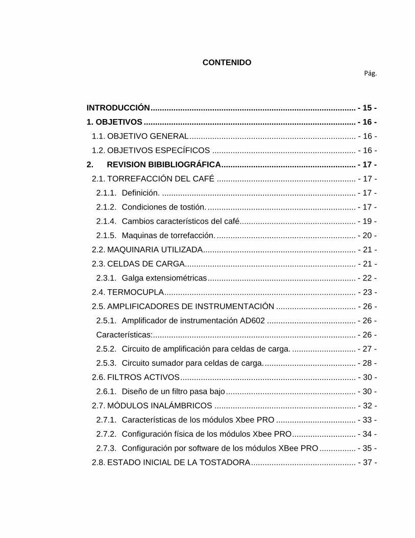
CONTENIDO
Pág.
INTRODUCCIÓN .......................................................................................... - 15 -
1. OBJETIVOS ............................................................................................. - 16 -
1.1. OBJETIVO GENERAL ......................................................................... - 16 -
1.2. OBJETIVOS ESPECÍFICOS ............................................................... - 16 -
2. REVISION BIBIBLIOGRÁFICA ........................................................... - 17 -
2.1. TORREFACCIÓN DEL CAFÉ ............................................................. - 17 -
2.1.1. Definición. ..................................................................................... - 17 -
2.1.2. Condiciones de tostión. ................................................................. - 17 -
2.1.4. Cambios característicos del café................................................... - 19 -
2.1.5. Maquinas de torrefacción. ............................................................. - 20 -
2.2. MAQUINARIA UTILIZADA ................................................................... - 21 -
2.3. CELDAS DE CARGA ........................................................................... - 21 -
2.3.1. Galga extensiométricas ................................................................. - 22 -
2.4. TERMOCUPLA .................................................................................... - 23 -
2.5. AMPLIFICADORES DE INSTRUMENTACIÓN ................................... - 26 -
2.5.1. Amplificador de instrumentación AD602 ....................................... - 26 -
Características:......................................................................................... - 26 -
2.5.2. Circuito de amplificación para celdas de carga. ............................ - 27 -
2.5.3. Circuito sumador para celdas de carga. ........................................ - 28 -
2.6. FILTROS ACTIVOS ............................................................................. - 30 -
2.6.1. Diseño de un filtro pasa bajo ......................................................... - 30 -
2.7. MÓDULOS INALÁMBRICOS .............................................................. - 32 -
2.7.1. Características de los módulos Xbee PRO ................................... - 33 -
2.7.2. Configuración física de los módulos Xbee PRO ............................ - 34 -
2.7.3. Configuración por software de los módulos XBee PRO ................ - 35 -
2.8. ESTADO INICIAL DE LA TOSTADORA .............................................. - 37 -
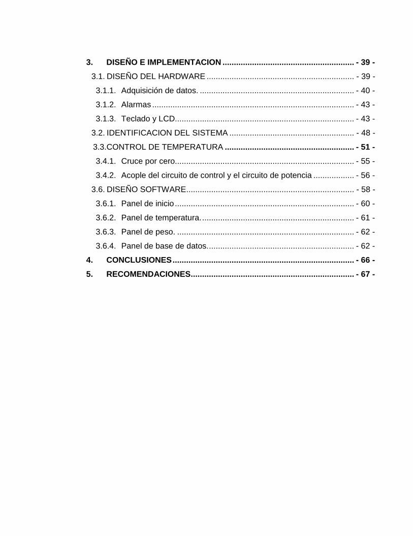
3. DISEÑO E IMPLEMENTACION .......................................................... - 39 -
3.1. DISEÑO DEL HARDWARE ................................................................. - 39 -
3.1.1. Adquisición de datos. .................................................................... - 40 -
3.1.2. Alarmas ......................................................................................... - 43 -
3.1.3. Teclado y LCD............................................................................... - 43 -
3.2. IDENTIFICACION DEL SISTEMA ....................................................... - 48 -
3.3.CONTROL DE TEMPERATURA ......................................................... - 51 -
3.4.1. Cruce por cero............................................................................... - 55 -
3.4.2. Acople del circuito de control y el circuito de potencia .................. - 56 -
3.6. DISEÑO SOFTWARE .......................................................................... - 58 -
3.6.1. Panel de inicio ............................................................................... - 60 -
3.6.2. Panel de temperatura. ................................................................... - 61 -
3.6.3. Panel de peso. .............................................................................. - 62 -
3.6.4. Panel de base de datos. ................................................................ - 62 -
4. CONCLUSIONES ................................................................................ - 66 -
5. RECOMENDACIONES ........................................................................ - 67 -
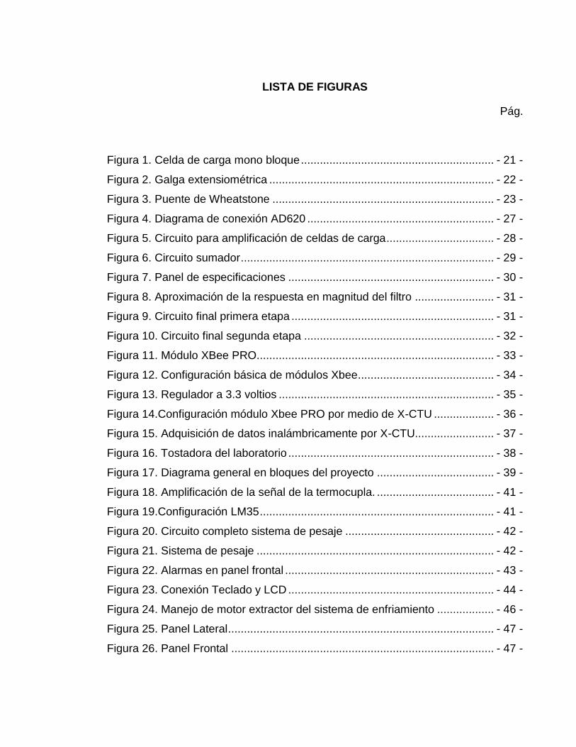
LISTA DE FIGURAS
Pág.
Figura 1. Celda de carga mono bloque ............................................................. - 21 -
Figura 2. Galga extensiométrica ....................................................................... - 22 -
Figura 3. Puente de Wheatstone ...................................................................... - 23 -
Figura 4. Diagrama de conexión AD620 ........................................................... - 27 -
Figura 5. Circuito para amplificación de celdas de carga .................................. - 28 -
Figura 6. Circuito sumador ................................................................................ - 29 -
Figura 7. Panel de especificaciones ................................................................. - 30 -
Figura 8. Aproximación de la respuesta en magnitud del filtro ......................... - 31 -
Figura 9. Circuito final primera etapa ................................................................ - 31 -
Figura 10. Circuito final segunda etapa ............................................................ - 32 -
Figura 11. Módulo XBee PRO........................................................................... - 33 -
Figura 12. Configuración básica de módulos Xbee........................................... - 34 -
Figura 13. Regulador a 3.3 voltios .................................................................... - 35 -
Figura 14.Configuración módulo Xbee PRO por medio de X-CTU ................... - 36 -
Figura 15. Adquisición de datos inalámbricamente por X-CTU......................... - 37 -
Figura 16. Tostadora del laboratorio ................................................................. - 38 -
Figura 17. Diagrama general en bloques del proyecto ..................................... - 39 -
Figura 18. Amplificación de la señal de la termocupla. ..................................... - 41 -
Figura 19.Configuración LM35 .......................................................................... - 41 -
Figura 20. Circuito completo sistema de pesaje ............................................... - 42 -
Figura 21. Sistema de pesaje ........................................................................... - 42 -
Figura 22. Alarmas en panel frontal .................................................................. - 43 -
Figura 23. Conexión Teclado y LCD ................................................................. - 44 -
Figura 24. Manejo de motor extractor del sistema de enfriamiento .................. - 46 -
Figura 25. Panel Lateral .................................................................................... - 47 -
Figura 26. Panel Frontal ................................................................................... - 47 -
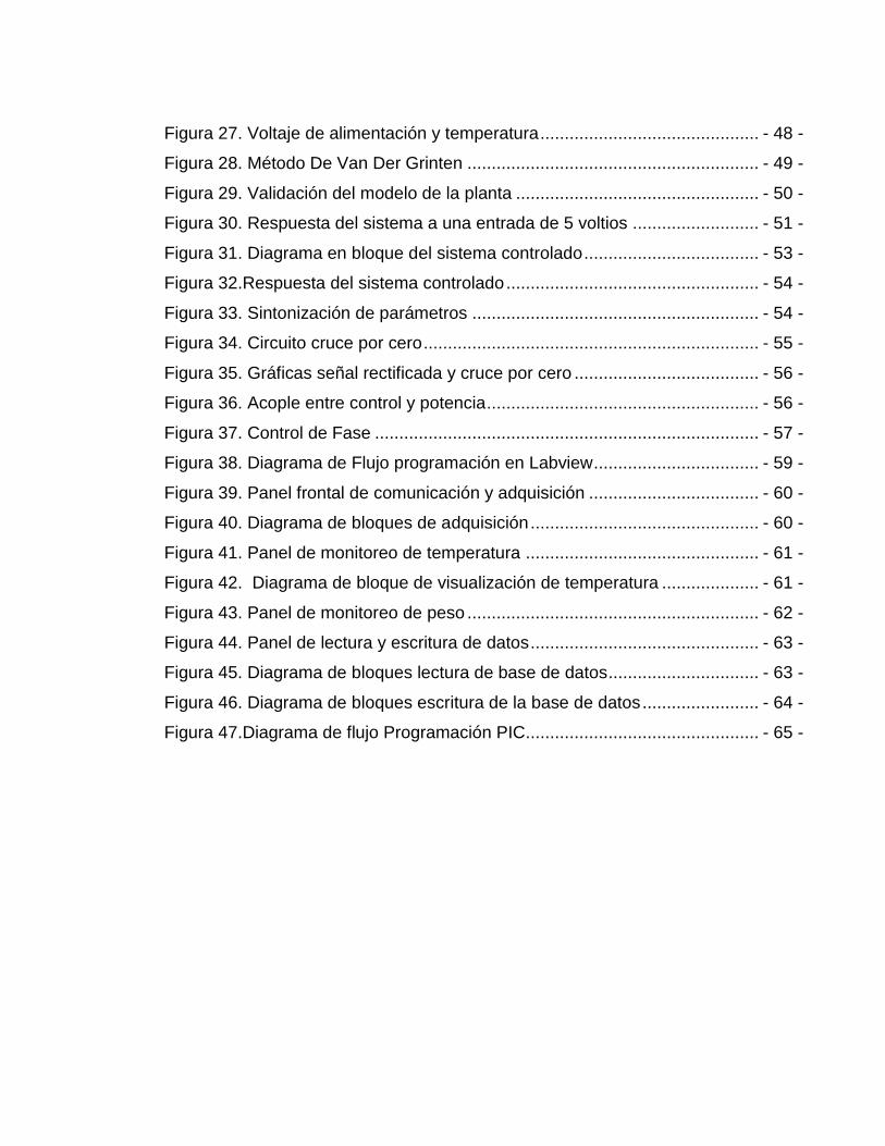
Figura 27. Voltaje de alimentación y temperatura ............................................. - 48 -
Figura 28. Método De Van Der Grinten ............................................................ - 49 -
Figura 29. Validación del modelo de la planta .................................................. - 50 -
Figura 30. Respuesta del sistema a una entrada de 5 voltios .......................... - 51 -
Figura 31. Diagrama en bloque del sistema controlado .................................... - 53 -
Figura 32.Respuesta del sistema controlado .................................................... - 54 -
Figura 33. Sintonización de parámetros ........................................................... - 54 -
Figura 34. Circuito cruce por cero ..................................................................... - 55 -
Figura 35. Gráficas señal rectificada y cruce por cero ...................................... - 56 -
Figura 36. Acople entre control y potencia ........................................................ - 56 -
Figura 37. Control de Fase ............................................................................... - 57 -
Figura 38. Diagrama de Flujo programación en Labview .................................. - 59 -
Figura 39. Panel frontal de comunicación y adquisición ................................... - 60 -
Figura 40. Diagrama de bloques de adquisición ............................................... - 60 -
Figura 41. Panel de monitoreo de temperatura ................................................ - 61 -
Figura 42. Diagrama de bloque de visualización de temperatura .................... - 61 -
Figura 43. Panel de monitoreo de peso ............................................................ - 62 -
Figura 44. Panel de lectura y escritura de datos ............................................... - 63 -
Figura 45. Diagrama de bloques lectura de base de datos ............................... - 63 -
Figura 46. Diagrama de bloques escritura de la base de datos ........................ - 64 -
Figura 47.Diagrama de flujo Programación PIC................................................ - 65 -
LISTA DE TABLAS
Pág.
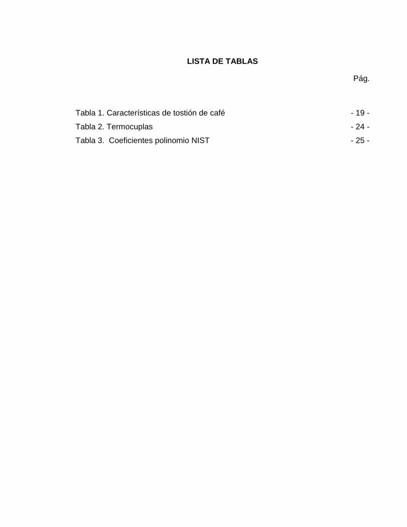
Tabla 1. Características de tostión de café - 19 -
Tabla 2. Termocuplas - 24 -
Tabla 3. Coeficientes polinomio NIST - 25 -
LISTA DE ANEXOS
Pág.
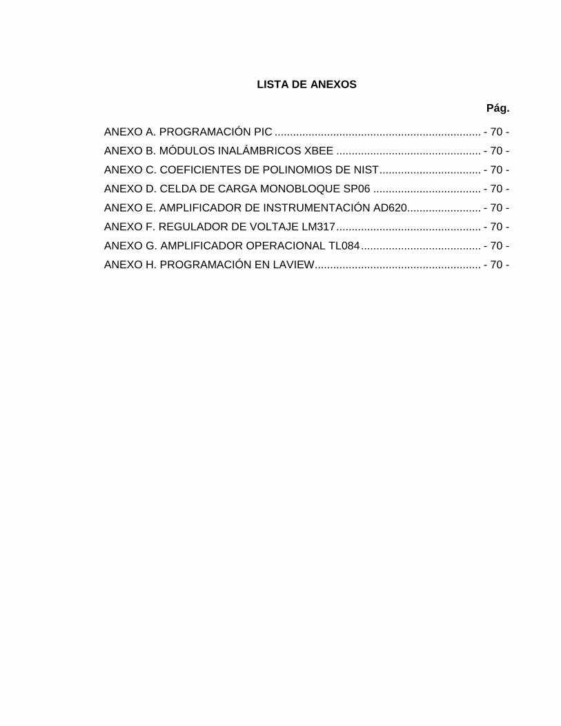
ANEXO A. PROGRAMACIÓN PIC ................................................................... - 70 -
ANEXO B. MÓDULOS INALÁMBRICOS XBEE ............................................... - 70 -
ANEXO C. COEFICIENTES DE POLINOMIOS DE NIST ................................. - 70 -
ANEXO D. CELDA DE CARGA MONOBLOQUE SP06 ................................... - 70 -
ANEXO E. AMPLIFICADOR DE INSTRUMENTACIÓN AD620........................ - 70 -
ANEXO F. REGULADOR DE VOLTAJE LM317 ............................................... - 70 -
ANEXO G. AMPLIFICADOR OPERACIONAL TL084 ....................................... - 70 -
ANEXO H. PROGRAMACIÓN EN LAVIEW...................................................... - 70 -
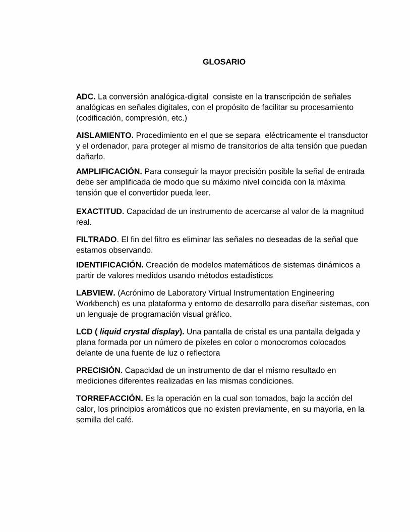
GLOSARIO
ADC. La conversión analógica-digital consiste en la transcripción de señales
analógicas en señales digitales, con el propósito de facilitar su procesamiento
(codificación, compresión, etc.)
AISLAMIENTO. Procedimiento en el que se separa eléctricamente el transductor
y el ordenador, para proteger al mismo de transitorios de alta tensión que puedan
dañarlo.
AMPLIFICACIÓN. Para conseguir la mayor precisión posible la señal de entrada
debe ser amplificada de modo que su máximo nivel coincida con la máxima
tensión que el convertidor pueda leer.
EXACTITUD. Capacidad de un instrumento de acercarse al valor de la magnitud
real.
FILTRADO. El fin del filtro es eliminar las señales no deseadas de la señal que
estamos observando.
IDENTIFICACIÓN. Creación de modelos matemáticos de sistemas dinámicos a
partir de valores medidos usando métodos estadísticos
LABVIEW. (Acrónimo de Laboratory Virtual Instrumentation Engineering
Workbench) es una plataforma y entorno de desarrollo para diseñar sistemas, con
un lenguaje de programación visual gráfico.
LCD ( liquid crystal display). Una pantalla de cristal es una pantalla delgada y
plana formada por un número de píxeles en color o monocromos colocados
delante de una fuente de luz o reflectora
PRECISIÓN. Capacidad de un instrumento de dar el mismo resultado en
mediciones diferentes realizadas en las mismas condiciones.
TORREFACCIÓN. Es la operación en la cual son tomados, bajo la acción del
calor, los principios aromáticos que no existen previamente, en su mayoría, en la
semilla del café.
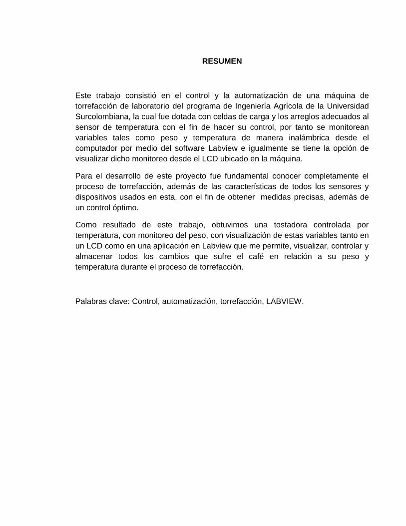
RESUMEN
Este trabajo consistió en el control y la automatización de una máquina de
torrefacción de laboratorio del programa de Ingeniería Agrícola de la Universidad
Surcolombiana, la cual fue dotada con celdas de carga y los arreglos adecuados al
sensor de temperatura con el fin de hacer su control, por tanto se monitorean
variables tales como peso y temperatura de manera inalámbrica desde el
computador por medio del software Labview e igualmente se tiene la opción de
visualizar dicho monitoreo desde el LCD ubicado en la máquina.
Para el desarrollo de este proyecto fue fundamental conocer completamente el
proceso de torrefacción, además de las características de todos los sensores y
dispositivos usados en esta, con el fin de obtener medidas precisas, además de
un control óptimo.
Como resultado de este trabajo, obtuvimos una tostadora controlada por
temperatura, con monitoreo del peso, con visualización de estas variables tanto en
un LCD como en una aplicación en Labview que me permite, visualizar, controlar y
almacenar todos los cambios que sufre el café en relación a su peso y
temperatura durante el proceso de torrefacción.
Palabras clave: Control, automatización, torrefacción, LABVIEW.

ABSTRACT
This work dealt with the control and automation of a laboratory coffee roaster of
Agricultural Engineering at Surcolombiana University, which was outfitted by load
cells and some modifications to sensor temperature with the purpose of making its
control, also were monitored every variables wirelessly through LABVIEW software
on the computer, furthermore offers the option of visualizing the monitoring on the
LCD that is in the machine.
For the development of this project was essential to know fully the roaster process,
also the characteristics of each sensor and device which was used in this machine,
for the purpose of acquiring accurate measurements and an optimum control.
As result of this work, we obtained a roast which was controlled by temperature,
with monitoring of weight, with visualization of these variables on a LCD and an
application on LABVIEW which offers the possibility of visualizing, controlling and
saving every changes that the coffee is suffering relation to its weight and
temperature during the roast process.
Keywords: Control, automation, roaster, LABVIEW.
- 15 -
INTRODUCCIÓN
Colombia hace parte de los principales productores de café verde en el mundo
siendo su producción y comercialización una de las principales fuentes de
ingresos para el país, es por ello que es de gran importancia la investigación que
se realiza actualmente en este campo con el fin de obtener un café de mejores
características constituyéndolo así, como un producto de alta calidad.
Es necesario tener en cuenta que la investigación realizada en el sector cafetero
es para la obtención de una mejor materia prima y así mismo de un mejor café
como producto final luego de múltiples procesos realizados con el fin de explotar al
máximo sus características de sabor, aroma, color y textura.
Actualmente el programa de Ingeniería Agrícola de la Universidad Surcolombiana
realiza investigaciones en relación al procesamiento del café, siendo de gran
importancia para la región, dado que el departamento del Huila en los últimos años
ha mostrado gran avance en cuanto a producción de cafés especiales,
catalogándose hoy en día como el primer productor de estos en el país, según el
Comité Nacional de Cafeteros de Colombia.
Es preciso destacar la importante labor realizada por el Programa de Ingeniería
Agrícola, el cual a través de los años ha avanzado en sus investigaciones en el
sector cafetero gracias a la adquisición de maquinaria apropiada para los
diferentes procesos realizados al grano como son fermentación, secado y
torrefacción.
Aunque el Programa ya contaba con una máquina de torrefacción de café
diseñada e implementada por un estudiante del programa de Ingeniería
Electrónica de la universidad Surcolombiana en el año 2004, la cual contaba con
un sistema de control de temperatura On-Off por medio de una termocupla y un
sistema de descarga y enfriamiento; lo que se desarrolla en esta tesis es el
mejoramiento de dicho sistema de control , además de monitorear el peso y la
temperatura del grano de manera inalámbrica y su posterior visualización en el
software Labview.
En relación a lo anterior, el desarrollo de este trabajo hace un aporte importante a
la investigación de este proceso en el sector cafetero, puesto que permite a los
investigadores acceder de una manera más fácil a los datos relacionados con el
proceso, con el fin de observar la dinámica de estas y determinar posteriormente
algunas características que permitirán aportar en el mejoramiento de la
producción del café como materia final.
- 16 -
1. OBJETIVOS
1.1. OBJETIVO GENERAL
Diseñar e implementar la automatización de una máquina de torrefacción
de café del laboratorio del Programa de Ingeniería Agrícola de la
Universidad Surcolombiana.
1.2. OBJETIVOS ESPECÍFICOS
Determinar la variable más adecuada a controlar dentro del proceso.
Crear una aplicación en el software LABVIEW que permita interactuar de
forma inalámbrica entre el usuario y la máquina, permitiendo de esta
manera la posibilidad de procesar y almacenar los correspondientes datos.
- 17 -
2. REVISION BIBIBLIOGRÁFICA
2.1. TORREFACCIÓN DEL CAFÉ
Desde la recolección hasta la obtención del café como producto final, observamos
diversos procesos los cuales siendo desarrollados de una manera adecuada,
conllevan a la obtención de un producto final de excelente calidad. Dentro de
estos procesos encontramos la torrefacción que es el proceso en donde se
explotarán al máximo las características desabor, aroma, color y textura del café,
debido a que este es sometido a altas temperaturas.
2.1.1. Definición.
La torrefacción del café es un proceso en el cual intervienen mecanismos de
transferencia de calor y de masa simultáneamente. Depende del tiempo y la
temperatura donde se inducen los cambios en el café verde, produciendo los
compuestos que originan el aroma característico, sabor, olor y cuerpo del café.1
2.1.2. Condiciones de tostión.
Durante el proceso de torrefacción es importante que tanto el café como la
maquinaria cumplan con algunas condiciones para lograr obtener un tostado de
excelente calidad, por lo tanto encontramos que se deben seguir las siguientes
indicaciones:
Café trillado y limpio de impurezas, libre de granos defectuosos.
Café seco con humedad entre 10% y 12 %.
Homogeneidad en el tamaño de los granos.
En necesario que el recipiente en el que se realiza la tostión esté en
constante movimiento para evitar la sobre torrefacción de los granos con el
fin de que no hayan pérdidas en sus condiciones óptimas de olor y sabor.
La tostión se debe hacer bajo calor uniforme y gradual. 1FEDERACIÓN NACIONAL DE CAFETEROS DE COLOMBIA. Revista cafetera de Colombia. Torrefacción o
tostada del café. Bogotá 1932
- 18 -
El tiempo y grado de tostión varían según el tipo de café, el tipo de equipo
utilizado, la intensidad de calor aplicado y de la forma en la que se transfiere
el calor.
Debido a algunos cambios físicos y químicos que más adelante se explicarán
detalladamente, el café sufre un aumento de volumen de hasta 2 veces su
volumen inicial, por lo tanto el equipo de tostión debe de quedar lo
suficientemente vacío para prever dicho aumento y facilitar el movimiento de
los granos.
Una vez terminada la tostión se debe contar con un sistema de enfriamiento
ya sea por medio de una corriente de aire frio a través de una malla o por
aspersión de agua conocido como Quenching, para impedir la sobre
torrefacción.
Al finalizar el proceso de torrefacción en muy importante que el café sea
almacenado en un lugar con condiciones adecuadas de temperatura y
humedad, para que no pierda sus características de aroma y sabor.
2.1.3. Fases de la torrefacción.
Debido a que la principal variable que interviene en este proceso es la temperatura
además de tener la mayor influencia sobre las cualidades del café, es esta la que
me indica con mayor exactitud las fases de la torrefacción, es así que:
Cuando la temperatura supera los 90º C el café comienza a sufrir cambios de
color pasando de verde a amarillo, además de iniciar también el desprendimiento
de vapor de agua; al llegar al punto de ebullición del agua, es decir a los 100ºC, el
agua que contiene el grado se evapora, por lo tanto hay una pérdida de peso.
Cerca de los 120ºC y 130ºC el grano se torna castaño y se empiezan a formar
algunos compuestos químicos. A partir de los 150ºC el olor es más característico y
se evidencia el aumento de volumen del grano; sobre los 180 ºC los azúcares y
almidones empiezan a transformarse, por lo tanto se empiezan a evidenciar mejor
sus características de aroma y sabor. A partir de los 200 ºC los gases de
combustión se desprenden, los granos se tornan marrón y tienen un aumento de
volumen de entre 40% y 60% debido a la crepitación de los granos como reacción
espontanea a su exposición a altas temperaturas. La temperatura óptima para la
tostión es la comprendida entre los 210ºC y 230ºC, por lo tanto, temperaturas por
encima de estas pueden producir sobre torrefacción, haciendo que pierda sus
cualidades, debido a que su aroma desaparece, deja de aumentar de volumen y
en algunos casos hasta llega a la carbonización. Finalmente para evitar dicha
- 19 -
carbonización y detener el proceso de torrefacción es necesario enfriar
inmediatamente el café por medio de aire frio o por medio de aspersión de agua.
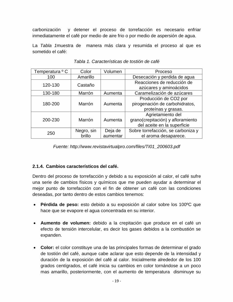
La Tabla 1muestra de manera más clara y resumida el proceso al que es
sometido el café:
Tabla 1. Características de tostión de café
Temperatura º C Color Volumen Proceso
100 Amarillo Desecación y perdida de agua
120-130 Castaño Reacciones de reducción de
azúcares y aminoácidos
130-180 Marrón Aumenta Caramelización de azúcares
180-200 Marrón Aumenta Producción de CO2 por
pirogenación de carbohidratos, proteínas y grasas.
200-230 Marrón Aumenta Agrietamiento del
grano(crepitación) y afloramiento del aceite en la superficie
250 Negro, sin
brillo Deja de
aumentar Sobre torrefacción, se carboniza y
el aroma desaparece.
Fuente: http://www.revistavirtualpro.com/files/TI01_200603.pdf
2.1.4. Cambios característicos del café.
Dentro del proceso de torrefacción y debido a su exposición al calor, el café sufre
una serie de cambios físicos y químicos que me pueden ayudar a determinar el
mejor punto de torrefacción con el fin de obtener un café con las condiciones
deseadas, por tanto dentro de estos cambios tenemos:
Pérdida de peso: esto debido a su exposición al calor sobre los 100ºC que
hace que se evapore el agua concentrada en su interior.
Aumento de volumen: debido a la crepitación que produce en el café un
efecto de tensión intercelular, es decir los gases debidos a la combustión se
expanden.
Color: el color constituye una de las principales formas de determinar el grado
de tostión del café, aunque cabe aclarar que esto depende de la intensidad y
duración de la exposición del café al calor. Inicialmente alrededor de los 100
grados centígrados, el café inicia su cambios en color tornándose a un poco
mas amarillo, posteriormente, con el aumento de temperatura disminuye su
- 20 -
peso y aumenta su volumen, así como también su color pasa a ser marrón
oscuro. Un indicio de sobretorrefación es un exagerado color marrón u oscuro
además de estar acompañado de un olor no característico.
Dureza: debido a los procesos de combustión, el café sufre un cambio en su
composición, haciendo que su capacidad de soportar presiones sea menor,
debido a que su estructura es más porosa.
Contenido de humedad: es muy importante durante estos procesos conocer
la humedad además de controlarla, puesto que si durante su almacenamiento
y empacado, su contenido de humedad no es el adecuado, puede conllevar a
aparición de hongos lo que significaría pérdida del café, por lo tanto se
convierte en un indicador de calidad del café.
Cambios químicos: como resultado de la exposición al calor, el café sufre
reacciones químicas que le dan algunas características o atributos a la bebida,
es decir son cambios relacionados con compuestos inherentes al olor y al
sabor dentro de las que encontramos proteínas, carbohidratos, grasas y
aceites, ácidos, taninos, minerales, dióxido de carbono, entre otros.
2.1.5. Máquinas de torrefacción.
Debido a la incorporación de las tecnologías en todos los procesos de producción
con el fin de mejorar la calidad además de reducir los tiempos y costos de
manufacturación, el proceso de tostado cambió de ser un proceso manual, en el
que simplemente el café dentro de un sartén era sometido a fuego y una persona
era la encargada de determinar el punto exacto de tostión, a un proceso en el cual
es posible, por medio de la medición de la temperatura del grano, determinar con
gran exactitud en mejor punto de tostión, además de asegurar que el café no sufra
torrefacción debido a que posee sistemas de enfriamiento adecuados.
De acuerdo a lo anterior, en la actualidad encontramos maquinas más robustas,
de mayor capacidad y con mejores características de rendimiento; actualmente
dichas máquinas son clasificadas comúnmente de acuerdo a su capacidad, por lo
tanto, tenemos dos grandes grupos: las de gran capacidad y las de baja
capacidad. El primer grupo corresponde a máquinas robustas utilizadas
industrialmente por su gran capacidad, utilizan regularmente gas o resistencias
calefactoras como medio calefactor, el segundo grupo corresponde a máquinas
más pequeñas usadas comúnmente en laboratorio y que usan resistencias
calefactoras como medio calefactor.
- 21 -
2.2. MAQUINARIA UTILIZADA
Siendo la torrefacción una de las etapas más importantes dentro del proceso de la
obtención del café como producto final, esta se ha convertido en un punto
importante de estudio e investigación con el fin de ayudar a mejorar dicho proceso,
por lo tanto la adecuación de sensores de temperatura y peso entre otros
constituyen un gran avance en el monitoreo y control del proceso de torrefacción.
Con el fin de optimizar aun más el proceso de torrefacción y contribuir a la
investigación en el país con respecto a este tema, nuestro proyecto tiene como
objeto de estudio una máquina de torrefacción diseñada e implementada por el
estudiante Yull Heilordt Henao del programa de Ingeniería Electrónica en el año
2004; dicho diseño está basando en la reunión de las características más
sobresalientes de algunas máquinas de torrefacción de las empresas más
importantes en el país dedicadas a este proceso en aquel año, como resultado de
esto, obtuvo una máquina tipo tambor con un sistema de descarga, un sistema de
enfriamiento y la integración de una termocupla tipo J para el control On/Off de la
temperatura.
Seguidamente veremos las características de los sensores y elementos usados en
el desarrollo de este proyecto de grado que serán incorporados a la máquina con
el fin de optimizar el proceso de torrefacción.
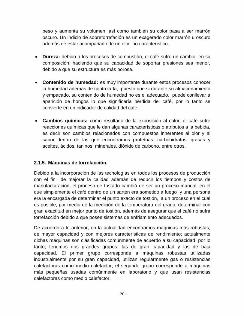
2.3. CELDAS DE CARGA
Debido a que el peso es un claro indicador en el proceso de tostión, escogimos
celdas de carga mono bloque (Ver ANEXO A) con capacidad de 40 kilos como la
que se muestra en la Figura 1.
Figura 1. Celda de carga mono bloque
Fuente:http://www.bci.co/Pesaje/celdas_de_carga/mono_bloque_max200kg/catalo
go_sp06/sp06.pdf
- 22 -
Una celda de carga es un transductor que convierte una fuerza a señales
eléctricas, su funcionamiento se basa en la conversión a señales eléctricas de la
deformación que sufren 4 galgas extensiométricas debido a la fuerza que se
quiere medir. Por tanto su principio de funcionamiento se centra en estas últimas.
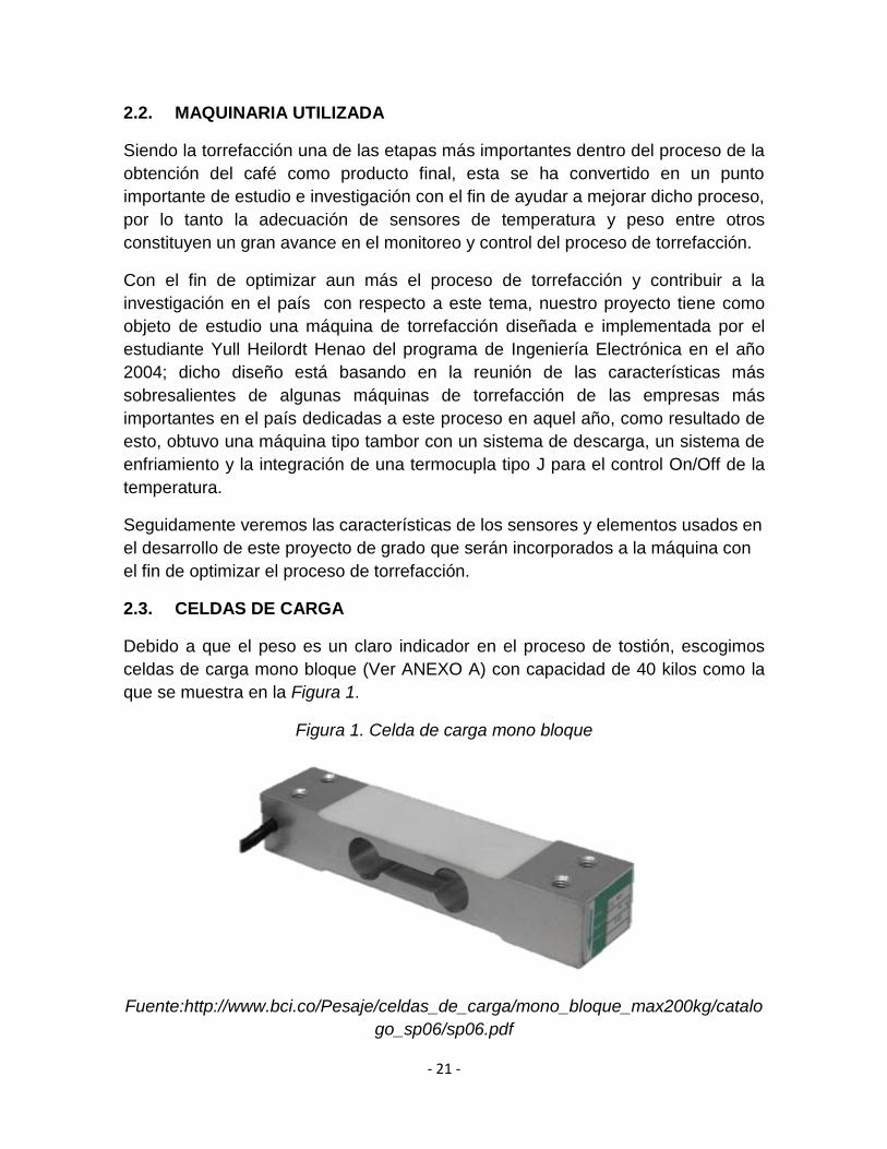
2.3.1. Galgas extensiométricas
Estos dispositivos son transductores que al aplicárseles fuerza, responde
modificando su resistencia eléctrica. Su principio de funcionamiento se basa en el
efecto piezorresistivo de metales y semiconductores, según el cual, su resistividad
varía en función de la deformación a la que están sometidos, el material de que
esta hecho y el diseño adoptado.
Si se considera un hilo metálico de longitud , sección transversal y resistividad
, su resistencia eléctrica es:
Si se le somete a un esfuerzo en dirección longitudinal, cada una de las tres
magnitudes que intervienen en el valor de cambia.2
El esquema general de una galga extensiométrica se observa en la Figura 2.
Figura 2. Galga extensiométrica
Fuente: http://www.unet.edu.ve/~ielectro/GALGAS1_archivos/image004.jpg
2 FERRERO, José María. Instrumentación Electrónica, Sensores. Universidad Politécnica de Valencia, España, 1994.
- 23 -
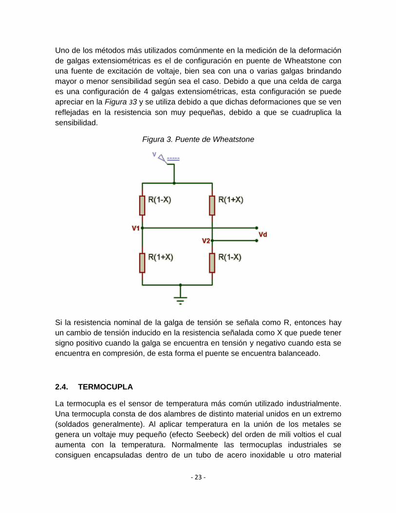
Uno de los métodos más utilizados comúnmente en la medición de la deformación
de galgas extensiométricas es el de configuración en puente de Wheatstone con
una fuente de excitación de voltaje, bien sea con una o varias galgas brindando
mayor o menor sensibilidad según sea el caso. Debido a que una celda de carga
es una configuración de 4 galgas extensiométricas, esta configuración se puede
apreciar en la Figura 33 y se utiliza debido a que dichas deformaciones que se ven
reflejadas en la resistencia son muy pequeñas, debido a que se cuadruplica la
sensibilidad.
Figura 3. Puente de Wheatstone
Si la resistencia nominal de la galga de tensión se señala como R, entonces hay
un cambio de tensión inducido en la resistencia señalada como X que puede tener
signo positivo cuando la galga se encuentra en tensión y negativo cuando esta se
encuentra en compresión, de esta forma el puente se encuentra balanceado.
2.4. TERMOCUPLA
La termocupla es el sensor de temperatura más común utilizado industrialmente.
Una termocupla consta de dos alambres de distinto material unidos en un extremo
(soldados generalmente). Al aplicar temperatura en la unión de los metales se
genera un voltaje muy pequeño (efecto Seebeck) del orden de mili voltios el cual
aumenta con la temperatura. Normalmente las termocuplas industriales se
consiguen encapsuladas dentro de un tubo de acero inoxidable u otro material
- 24 -
(vaina), en un extremo está la unión caliente y en el otro el terminal eléctrico de la
unión fría, protegido dentro de una caja redonda de aluminio (cabezal).3
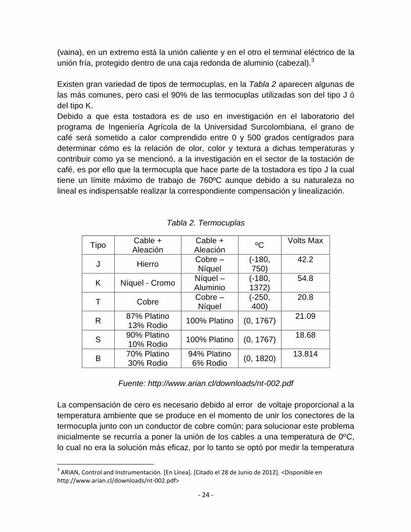
Existen gran variedad de tipos de termocuplas, en la Tabla 2 aparecen algunas de
las más comunes, pero casi el 90% de las termocuplas utilizadas son del tipo J ó
del tipo K.
Debido a que esta tostadora es de uso en investigación en el laboratorio del
programa de Ingeniería Agrícola de la Universidad Surcolombiana, el grano de
café será sometido a calor comprendido entre 0 y 500 grados centígrados para
determinar cómo es la relación de olor, color y textura a dichas temperaturas y
contribuir como ya se mencionó, a la investigación en el sector de la tostación de
café, es por ello que la termocupla que hace parte de la tostadora es tipo J la cual
tiene un límite máximo de trabajo de 760ºC aunque debido a su naturaleza no
lineal es indispensable realizar la correspondiente compensación y linealización.
Tabla 2. Termocuplas
Tipo Cable + Aleación
Cable + Aleación
ºC Volts Max
J Hierro Cobre – Níquel
(-180, 750)
42.2
K Níquel - Cromo Níquel – Aluminio
(-180, 1372)
54.8
T Cobre Cobre – Níquel
(-250, 400)
20.8
R 87% Platino 13% Rodio
100% Platino (0, 1767) 21.09
S 90% Platino 10% Rodio
100% Platino (0, 1767) 18.68
B 70% Platino 30% Rodio
94% Platino 6% Rodio
(0, 1820) 13.814
Fuente: http://www.arian.cl/downloads/nt-002.pdf
La compensación de cero es necesario debido al error de voltaje proporcional a la
temperatura ambiente que se produce en el momento de unir los conectores de la
termocupla junto con un conductor de cobre común; para solucionar este problema
inicialmente se recurría a poner la unión de los cables a una temperatura de 0ºC,
lo cual no era la solución más eficaz, por lo tanto se optó por medir la temperatura
3 ARIAN, Control and Instrumentación. [En Línea]. [Citado el 28 de Junio de 2012]. <Disponible en
http://www.arian.cl/downloads/nt-002.pdf>
- 25 -
ambiente por medio de un sensor de temperatura LM35, y restarlo a la
suministrada por la termocupla después de la linealización.
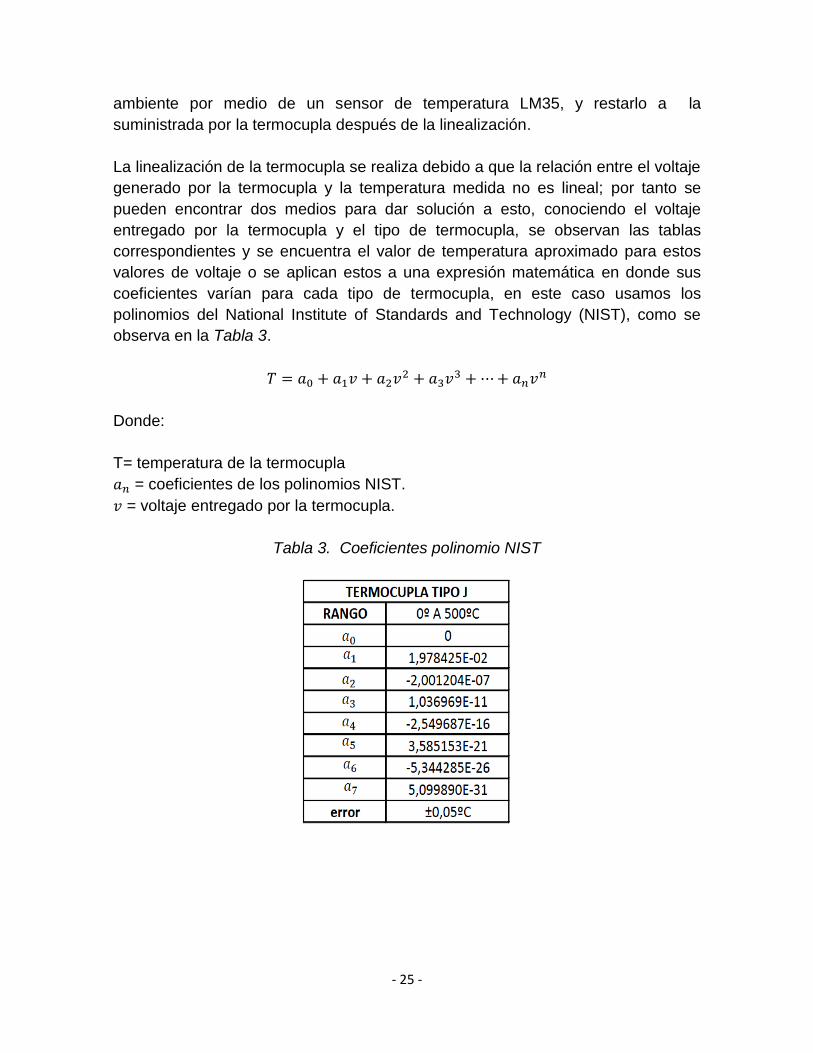
La linealización de la termocupla se realiza debido a que la relación entre el voltaje
generado por la termocupla y la temperatura medida no es lineal; por tanto se
pueden encontrar dos medios para dar solución a esto, conociendo el voltaje
entregado por la termocupla y el tipo de termocupla, se observan las tablas
correspondientes y se encuentra el valor de temperatura aproximado para estos
valores de voltaje o se aplican estos a una expresión matemática en donde sus
coeficientes varían para cada tipo de termocupla, en este caso usamos los
polinomios del National Institute of Standards and Technology (NIST), como se
observa en la Tabla 3.
Donde:
T= temperatura de la termocupla
= coeficientes de los polinomios NIST.
= voltaje entregado por la termocupla.
Tabla 3. Coeficientes polinomio NIST
- 26 -
2.5. AMPLIFICADORES DE INSTRUMENTACIÓN
Debido a que la señal que envían las celdas de carga es del orden de los mili
voltios, se debe hacer la adecuación de dicha señal para que esté dentro del
rango de los 0 a 5 voltios; dicha adecuación se hace con la ayuda del amplificador
de instrumentación AD602 el cual por medio de una resistencia proporciona la
amplificación necesaria.
En nuestro sistema de pesaje contamos con 4 celdas de carga de características
especificadas en el ANEXO B; la señal eléctrica que proporciona cada una de
estas es debidamente amplificada, es decir dicha adecuación se realiza de igual
forma para las cuatro celdas de carga con el fin de hacer que el sistema sea
balanceado.
2.5.1. Amplificador de instrumentación AD602
Características4:
Fácil uso:
• Requiere solo una resistencia externa para ajustar la ganancia de 1 a 1000.
• Amplio rango de alimentación (+- 2.3 V a +- 18 V).
• Mayor rendimiento que tres Amplificadores operacionales.
• Bajo consumo, 1.3 mA corriente de alimentación máxima.
Excelente rendimiento en DC:
• Voltaje offset de salida máximo de 50uV
• Relación de cambio de la intensidad de polarización de entrada en función de la
temperatura: máx. 0.6 uV/ºC
Bajo ruido
Excelentes especificaciones AC:
• Ancho de banda de 120 KHz para una ganancia de 100.
Aplicaciones:
• Balanzas.
• ECG e instrumentación medica.
• Sistemas de adquisición de datos.
4ANALOG DEVICES, Semiconductors and Signal Processing. [En Línea]. [Citado el 28 de Junio de 2012.].
<Disponible en http://users.ece.utexas.edu/~valvano/Datasheets/AD620.pdf>
- 27 -
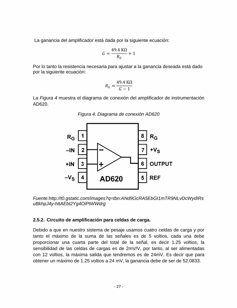
La ganancia del amplificador está dada por la siguiente ecuación:
Por lo tanto la resistencia necesaria para ajustar a la ganancia deseada está dado por la siguiente ecuación:
La Figura 4 muestra el diagrama de conexión del amplificador de instrumentación
AD620.
Figura 4. Diagrama de conexión AD620
Fuente:http://t0.gstatic.com/images?q=tbn:ANd9GcRA5EbGI1mTR9NLvDcWydIRsuBkhpJ4y-httAEbt2Yg4OiPtWWdrg 2.5.2. Circuito de amplificación para celdas de carga.
Debido a que en nuestro sistema de pesaje usamos cuatro celdas de carga y por
tanto el máximo de la suma de las señales es de 5 voltios, cada una debe
proporcionar una cuarta parte del total de la señal, es decir 1.25 voltios, la
sensibilidad de las celdas de cargas es de 2mV/V, por tanto, al ser alimentadas
con 12 voltios, la máxima salida que tendremos es de 24mV. Es decir que para
obtener un máximo de 1.25 voltios a 24 mV, la ganancia debe de ser de 52.0833.
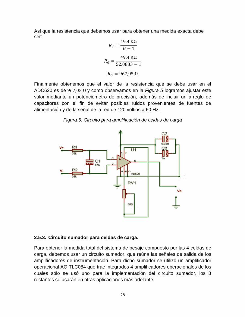
- 28 -
Así que la resistencia que debemos usar para obtener una medida exacta debe ser:
Finalmente obtenemos que el valor de la resistencia que se debe usar en el
ADC620 es de y como observamos en la Figura 5 logramos ajustar este
valor mediante un potenciómetro de precisión, además de incluir un arreglo de
capacitores con el fin de evitar posibles ruidos provenientes de fuentes de
alimentación y de la señal de la red de 120 voltios a 60 Hz.
Figura 5. Circuito para amplificación de celdas de carga
2.5.3. Circuito sumador para celdas de carga.
Para obtener la medida total del sistema de pesaje compuesto por las 4 celdas de
carga, debemos usar un circuito sumador, que reúna las señales de salida de los
amplificadores de instrumentación. Para dicho sumador se utilizó un amplificador
operacional AO TLC084 que trae integrados 4 amplificadores operacionales de los
cuales sólo se usó uno para la implementación del circuito sumador, los 3
restantes se usarán en otras aplicaciones más adelante.
- 29 -
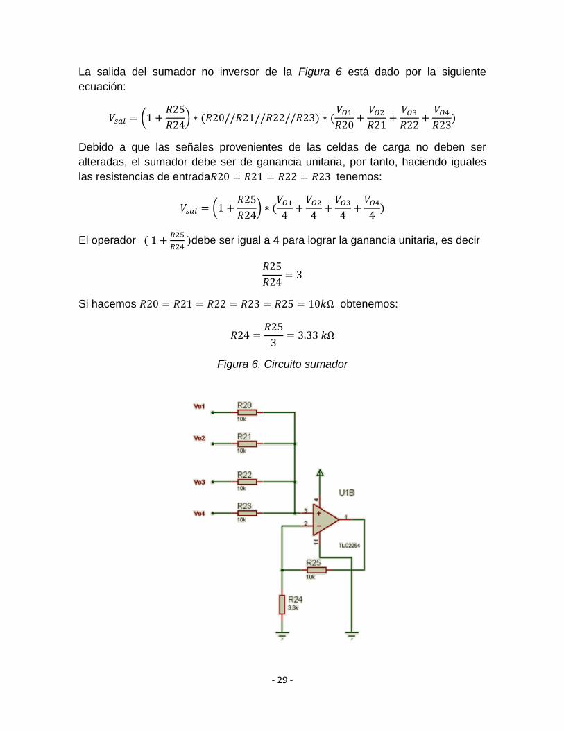
La salida del sumador no inversor de la Figura 6 está dado por la siguiente
ecuación:
(
)
Debido a que las señales provenientes de las celdas de carga no deben ser
alteradas, el sumador debe ser de ganancia unitaria, por tanto, haciendo iguales
las resistencias de entrada tenemos:
(
)
El operador
debe ser igual a 4 para lograr la ganancia unitaria, es decir
Si hacemos obtenemos:
Figura 6. Circuito sumador
- 30 -
2.6. FILTROS ACTIVOS
Debido a que es muy probable que haya ruido en la adquisición de los datos de
peso insertado por las celdas de carga, además de eso amplificado y sumado
debido a las etapas implementadas para la adecuación de las celdas de carga, es
necesario y recomendable implementar un filtro activo que filtre dicha señal y que
proporcione como salida, sólo la componente DC de dicha señal.
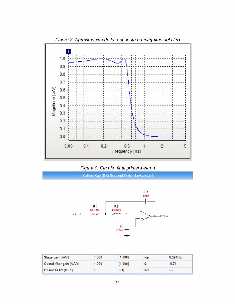
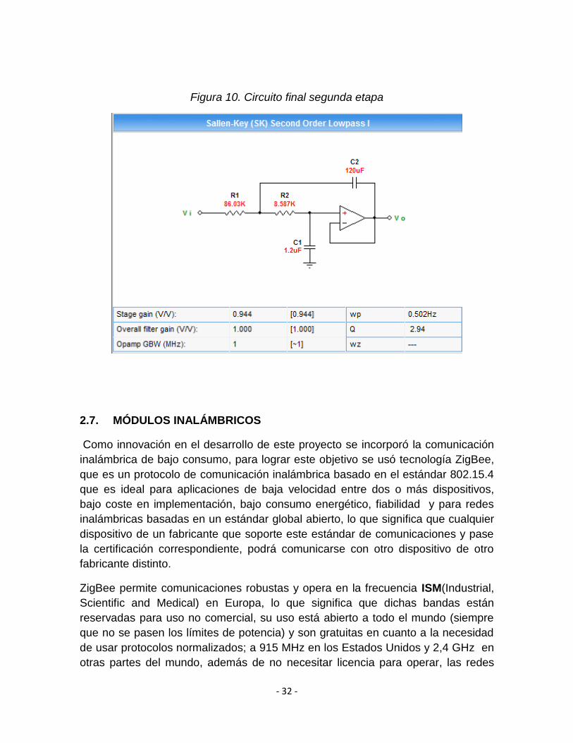
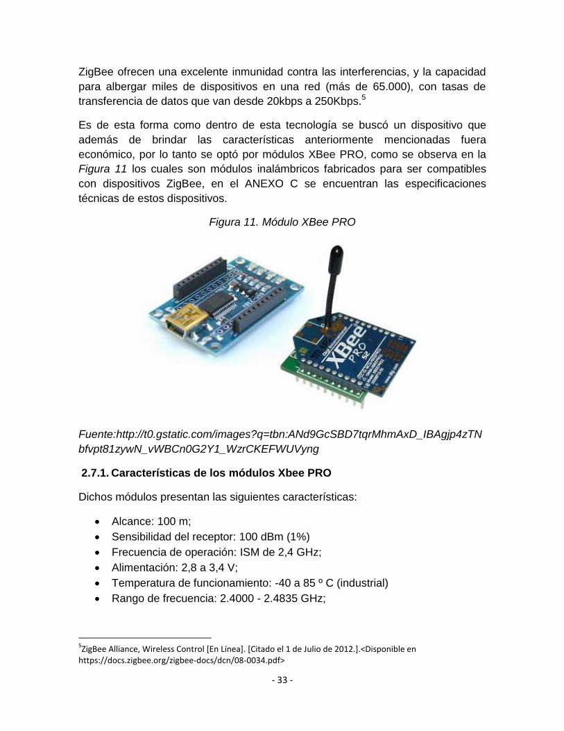
2.6.1. Diseño de un filtro pasa bajo
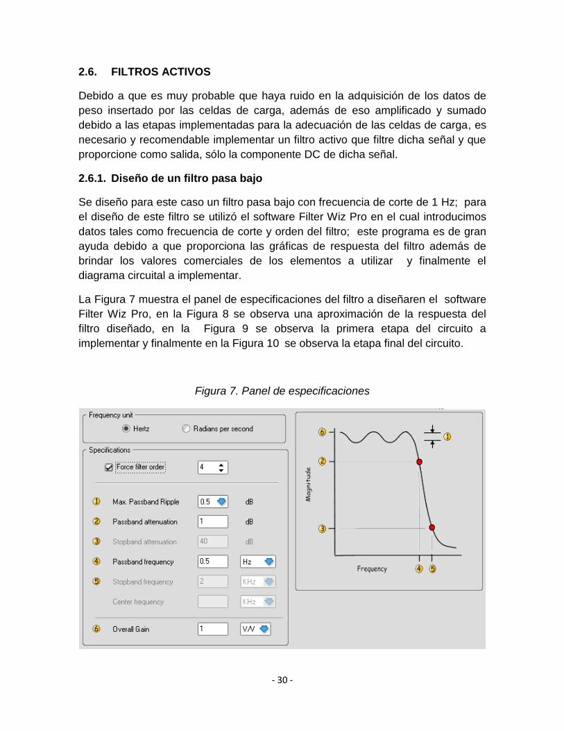
Se diseño para este caso un filtro pasa bajo con frecuencia de corte de 1 Hz; para
el diseño de este filtro se utilizó el software Filter Wiz Pro en el cual introducimos
datos tales como frecuencia de corte y orden del filtro; este programa es de gran
ayuda debido a que proporciona las gráficas de respuesta del filtro además de
brindar los valores comerciales de los elementos a utilizar y finalmente el
diagrama circuital a implementar.
La Figura 7 muestra el panel de especificaciones del filtro a diseñaren el software
Filter Wiz Pro, en la Figura 8 se observa una aproximación de la respuesta del
filtro diseñado, en la Figura 9 se observa la primera etapa del circuito a
implementar y finalmente en la Figura 10 se observa la etapa final del circuito.
Figura 7. Panel de especificaciones
- 31 -
Figura 8. Aproximación de la respuesta en magnitud del filtro
Figura 9. Circuito final primera etapa
- 32 -
Figura 10. Circuito final segunda etapa
2.7. MÓDULOS INALÁMBRICOS
Como innovación en el desarrollo de este proyecto se incorporó la comunicación
inalámbrica de bajo consumo, para lograr este objetivo se usó tecnología ZigBee,
que es un protocolo de comunicación inalámbrica basado en el estándar 802.15.4
que es ideal para aplicaciones de baja velocidad entre dos o más dispositivos,
bajo coste en implementación, bajo consumo energético, fiabilidad y para redes
inalámbricas basadas en un estándar global abierto, lo que significa que cualquier
dispositivo de un fabricante que soporte este estándar de comunicaciones y pase
la certificación correspondiente, podrá comunicarse con otro dispositivo de otro
fabricante distinto.
ZigBee permite comunicaciones robustas y opera en la frecuencia ISM(Industrial,
Scientific and Medical) en Europa, lo que significa que dichas bandas están
reservadas para uso no comercial, su uso está abierto a todo el mundo (siempre
que no se pasen los límites de potencia) y son gratuitas en cuanto a la necesidad
de usar protocolos normalizados; a 915 MHz en los Estados Unidos y 2,4 GHz en
otras partes del mundo, además de no necesitar licencia para operar, las redes
- 33 -
ZigBee ofrecen una excelente inmunidad contra las interferencias, y la capacidad
para albergar miles de dispositivos en una red (más de 65.000), con tasas de
transferencia de datos que van desde 20kbps a 250Kbps.5
Es de esta forma como dentro de esta tecnología se buscó un dispositivo que
además de brindar las características anteriormente mencionadas fuera
económico, por lo tanto se optó por módulos XBee PRO, como se observa en la
Figura 11 los cuales son módulos inalámbricos fabricados para ser compatibles
con dispositivos ZigBee, en el ANEXO C se encuentran las especificaciones
técnicas de estos dispositivos.
Figura 11. Módulo XBee PRO
Fuente:http://t0.gstatic.com/images?q=tbn:ANd9GcSBD7tqrMhmAxD_IBAgjp4zTN
bfvpt81zywN_vWBCn0G2Y1_WzrCKEFWUVyng
2.7.1. Características de los módulos Xbee PRO
Dichos módulos presentan las siguientes características:
Alcance: 100 m;
Sensibilidad del receptor: 100 dBm (1%)
Frecuencia de operación: ISM de 2,4 GHz;
Alimentación: 2,8 a 3,4 V;
Temperatura de funcionamiento: -40 a 85 º C (industrial)
Rango de frecuencia: 2.4000 - 2.4835 GHz;
5ZigBee Alliance, Wireless Control [En Línea]. [Citado el 1 de Julio de 2012.].<Disponible en
https://docs.zigbee.org/zigbee-docs/dcn/08-0034.pdf>
- 34 -
Bajo consumo <50mA cuando está en funcionamiento y <10uA cuando
están en modo sleep.
Interfaz serial.
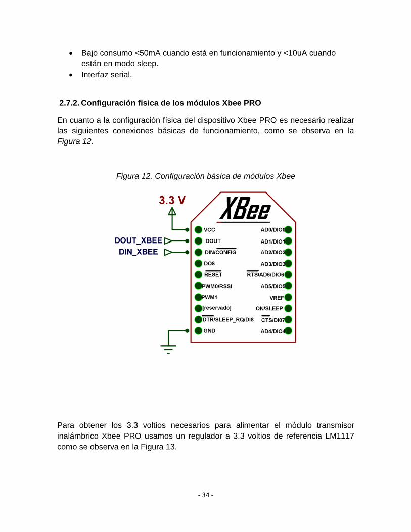
2.7.2. Configuración física de los módulos Xbee PRO
En cuanto a la configuración física del dispositivo Xbee PRO es necesario realizar
las siguientes conexiones básicas de funcionamiento, como se observa en la
Figura 12.
Figura 12. Configuración básica de módulos Xbee
Para obtener los 3.3 voltios necesarios para alimentar el módulo transmisor
inalámbrico Xbee PRO usamos un regulador a 3.3 voltios de referencia LM1117
como se observa en la Figura 13.
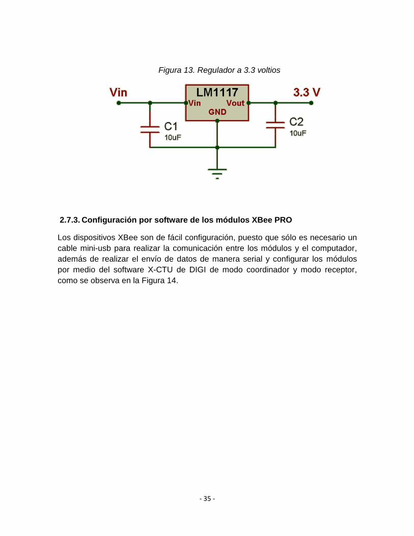
- 35 -
Figura 13. Regulador a 3.3 voltios
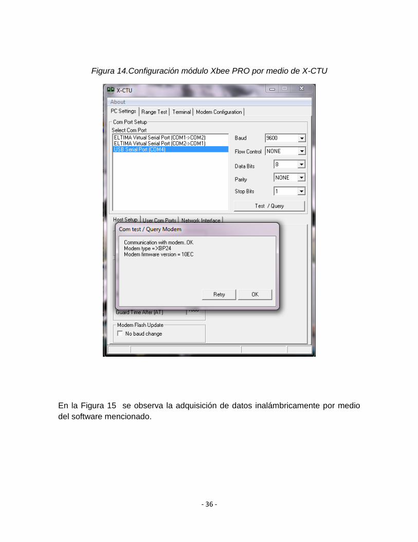
2.7.3. Configuración por software de los módulos XBee PRO
Los dispositivos XBee son de fácil configuración, puesto que sólo es necesario un
cable mini-usb para realizar la comunicación entre los módulos y el computador,
además de realizar el envío de datos de manera serial y configurar los módulos
por medio del software X-CTU de DIGI de modo coordinador y modo receptor,
como se observa en la Figura 14.
- 36 -
Figura 14.Configuración módulo Xbee PRO por medio de X-CTU
En la Figura 15 se observa la adquisición de datos inalámbricamente por medio
del software mencionado.
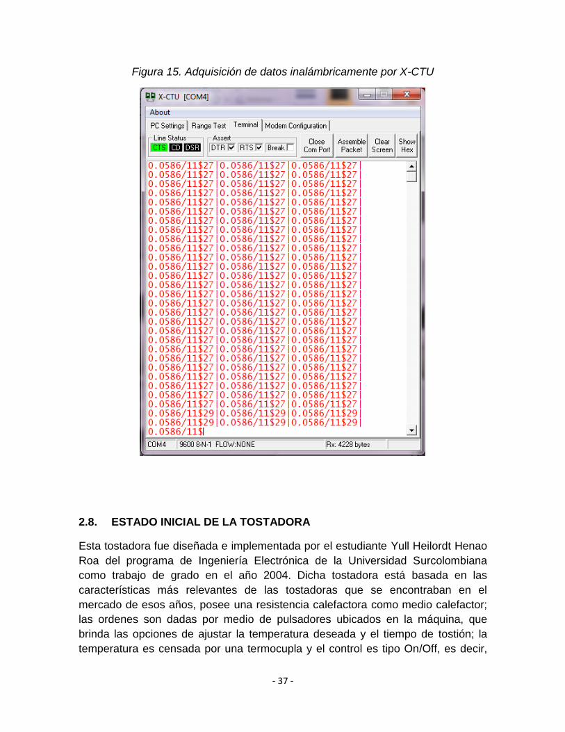
- 37 -
Figura 15. Adquisición de datos inalámbricamente por X-CTU
2.8. ESTADO INICIAL DE LA TOSTADORA
Esta tostadora fue diseñada e implementada por el estudiante Yull Heilordt Henao
Roa del programa de Ingeniería Electrónica de la Universidad Surcolombiana
como trabajo de grado en el año 2004. Dicha tostadora está basada en las
características más relevantes de las tostadoras que se encontraban en el
mercado de esos años, posee una resistencia calefactora como medio calefactor;
las ordenes son dadas por medio de pulsadores ubicados en la máquina, que
brinda las opciones de ajustar la temperatura deseada y el tiempo de tostión; la
temperatura es censada por una termocupla y el control es tipo On/Off, es decir,
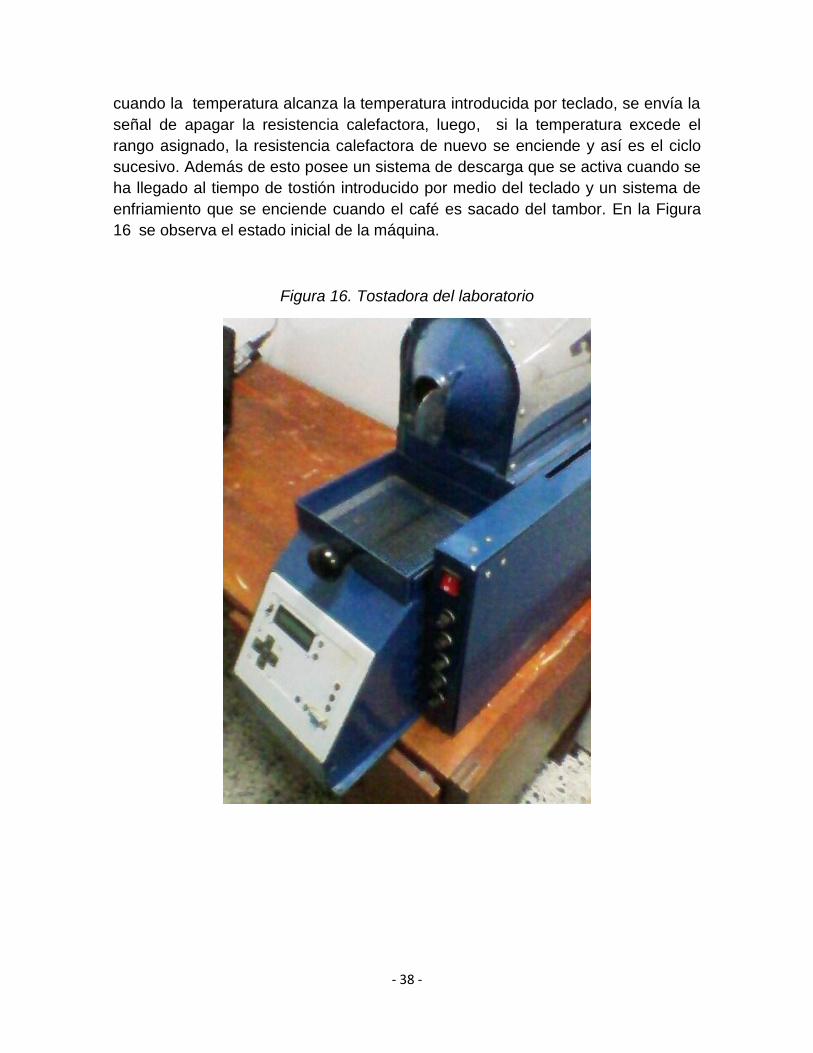
- 38 -
cuando la temperatura alcanza la temperatura introducida por teclado, se envía la
señal de apagar la resistencia calefactora, luego, si la temperatura excede el
rango asignado, la resistencia calefactora de nuevo se enciende y así es el ciclo
sucesivo. Además de esto posee un sistema de descarga que se activa cuando se
ha llegado al tiempo de tostión introducido por medio del teclado y un sistema de
enfriamiento que se enciende cuando el café es sacado del tambor. En la Figura
16 se observa el estado inicial de la máquina.
Figura 16. Tostadora del laboratorio
- 39 -
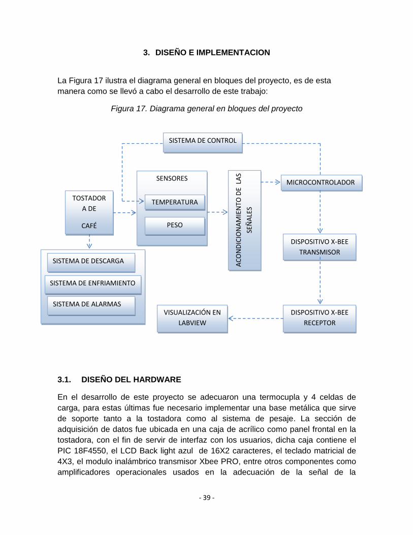
3. DISEÑO E IMPLEMENTACION
La Figura 17 ilustra el diagrama general en bloques del proyecto, es de esta
manera como se llevó a cabo el desarrollo de este trabajo:
Figura 17. Diagrama general en bloques del proyecto
3.1. DISEÑO DEL HARDWARE
En el desarrollo de este proyecto se adecuaron una termocupla y 4 celdas de
carga, para estas últimas fue necesario implementar una base metálica que sirve
de soporte tanto a la tostadora como al sistema de pesaje. La sección de
adquisición de datos fue ubicada en una caja de acrílico como panel frontal en la
tostadora, con el fin de servir de interfaz con los usuarios, dicha caja contiene el
PIC 18F4550, el LCD Back light azul de 16X2 caracteres, el teclado matricial de
4X3, el modulo inalámbrico transmisor Xbee PRO, entre otros componentes como
amplificadores operacionales usados en la adecuación de la señal de la
TOSTADOR
A DE
CAFÉ
SENSORES
TEMPERATURA
PESO
AC
ON
DIC
ION
AM
IEN
TO D
E L
AS
SEÑ
ALE
S
MICROCONTROLADOR
DISPOSITIVO X-BEE
TRANSMISOR
SISTEMA DE CONTROL
DISPOSITIVO X-BEE
RECEPTOR
VISUALIZACIÓN EN
LABVIEW
SISTEMA DE DESCARGA
SISTEMA DE ENFRIAMIENTO
SISTEMA DE ALARMAS
- 40 -
termocupla, integrados 555 para el manejo de las señales de alarmas y los opto
acopladores usados para aislar el circuito de control con el circuito de la carga.
Adicionalmente, fue necesaria la implementación de una nueva caja que me
permite ubicar de forma segura el modulo inalámbrico receptor de datos.
3.1.1. Adquisición de datos.
Los datos de temperatura para el control de temperatura de la resistencia
calefactora, los datos del peso y las señales provenientes de los sensores ópticos
de inicio y fin de carrera para el sistema de descarga son adquiridos por medio del
PIC 18F4550.
Aunque la tostadora de café inicialmente traía adecuada la señal de la termocupla,
decidimos implementar una nueva, debido a que la existente poseía algunos
problemas en las lecturas debido al deterioro de los elementos, de tal forma que
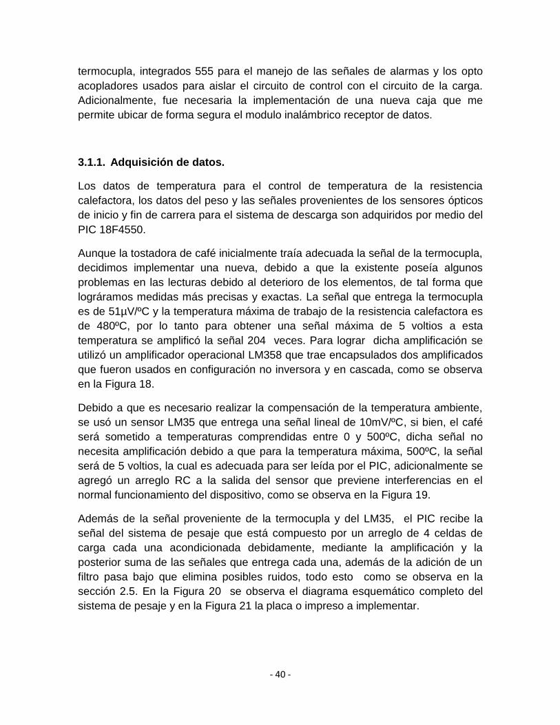
lográramos medidas más precisas y exactas. La señal que entrega la termocupla
es de 51µV/ºC y la temperatura máxima de trabajo de la resistencia calefactora es
de 480ºC, por lo tanto para obtener una señal máxima de 5 voltios a esta
temperatura se amplificó la señal 204 veces. Para lograr dicha amplificación se
utilizó un amplificador operacional LM358 que trae encapsulados dos amplificados
que fueron usados en configuración no inversora y en cascada, como se observa
en la Figura 18.
Debido a que es necesario realizar la compensación de la temperatura ambiente,
se usó un sensor LM35 que entrega una señal lineal de 10mV/ºC, si bien, el café
será sometido a temperaturas comprendidas entre 0 y 500ºC, dicha señal no
necesita amplificación debido a que para la temperatura máxima, 500ºC, la señal
será de 5 voltios, la cual es adecuada para ser leída por el PIC, adicionalmente se
agregó un arreglo RC a la salida del sensor que previene interferencias en el
normal funcionamiento del dispositivo, como se observa en la Figura 19.
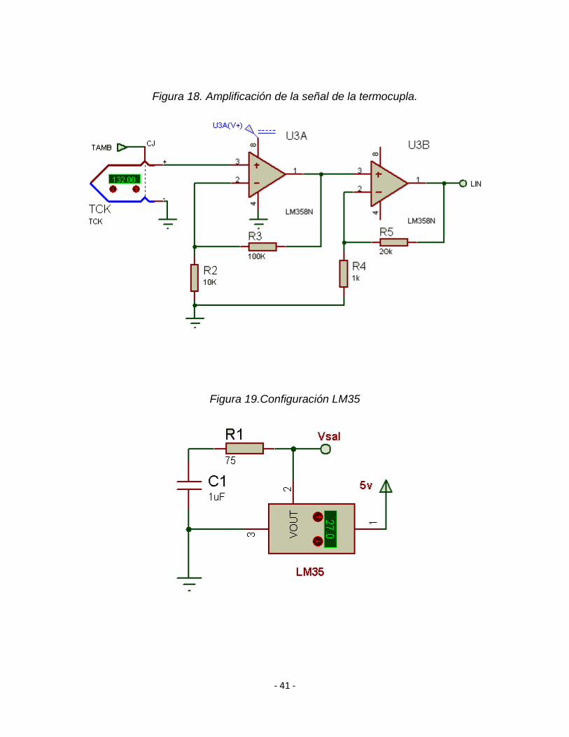
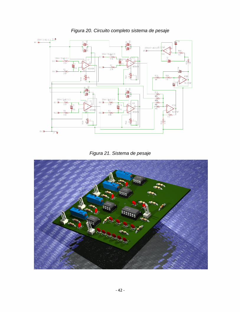
Además de la señal proveniente de la termocupla y del LM35, el PIC recibe la
señal del sistema de pesaje que está compuesto por un arreglo de 4 celdas de
carga cada una acondicionada debidamente, mediante la amplificación y la
posterior suma de las señales que entrega cada una, además de la adición de un
filtro pasa bajo que elimina posibles ruidos, todo esto como se observa en la
sección 2.5. En la Figura 20 se observa el diagrama esquemático completo del
sistema de pesaje y en la Figura 21 la placa o impreso a implementar.
- 41 -
Figura 18. Amplificación de la señal de la termocupla.
Figura 19.Configuración LM35
- 42 -
Figura 20. Circuito completo sistema de pesaje
Figura 21. Sistema de pesaje
- 43 -
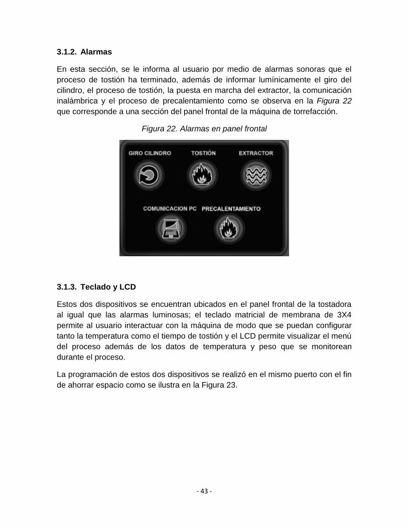
3.1.2. Alarmas
En esta sección, se le informa al usuario por medio de alarmas sonoras que el
proceso de tostión ha terminado, además de informar lumínicamente el giro del
cilindro, el proceso de tostión, la puesta en marcha del extractor, la comunicación
inalámbrica y el proceso de precalentamiento como se observa en la Figura 22
que corresponde a una sección del panel frontal de la máquina de torrefacción.
Figura 22. Alarmas en panel frontal
3.1.3. Teclado y LCD
Estos dos dispositivos se encuentran ubicados en el panel frontal de la tostadora
al igual que las alarmas luminosas; el teclado matricial de membrana de 3X4
permite al usuario interactuar con la máquina de modo que se puedan configurar
tanto la temperatura como el tiempo de tostión y el LCD permite visualizar el menú
del proceso además de los datos de temperatura y peso que se monitorean
durante el proceso.
La programación de estos dos dispositivos se realizó en el mismo puerto con el fin
de ahorrar espacio como se ilustra en la Figura 23.
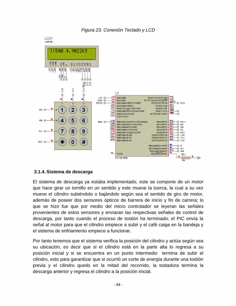
- 44 -
Figura 23. Conexión Teclado y LCD
3.1.4. Sistema de descarga
El sistema de descarga ya estaba implementado, este se compone de un motor
que hace girar un tornillo en un sentido y este mueve la tuerca, la cual a su vez
mueve el cilindro subiéndolo o bajándolo según sea el sentido de giro de motor,
además de poseer dos sensores ópticos de barrera de inicio y fin de carrera; lo
que se hizo fue que por medio del micro controlador se leyeran las señales
provenientes de estos sensores y enviaran las respectivas señales de control de
descarga, por tanto cuando el proceso de tostión ha terminado, el PIC envía la
señal al motor para que el cilindro empiece a subir y el café caiga en la bandeja y
el sistema de enfriamiento empiece a funcionar.
Por tanto tenemos que el sistema verifica la posición del cilindro y actúa según sea
su ubicación, es decir que si el cilindro está en la parte alta lo regresa a su
posición inicial y si se encuentra en un punto intermedio termina de subir el
cilindro, esto para garantizar que si ocurrió un corte de energía durante una tostión
previa y el cilindro quedo en la mitad del recorrido, la tostadora termina la
descarga anterior y regresa el cilindro a la posición inicial.
- 45 -
3.1.5. Sistema de enfriamiento
La tostadora de café está dotada con un sistema de enfriamiento el cual consta de
un conducto con dos recamaras (tolvas) que se conectan a un extractor. La
primera recamara es donde se enfría el grano y la segunda está ubicada debajo
de la resistencia y el cilindro donde se realiza la tostión. Se acondicionó un
pequeño motor DC, el cual viene adecuado para sacar un pequeño pistón de unos
4 cm aproximadamente cuando se polariza en directo (+ 12 V DC) y regresa a su
posición original con una polarización inversa.
El funcionamiento del sistema consiste en abrir la compuerta 1 y encender el
extractor en el momento en que el café tostado se encuentre en la bandeja
(posición 1) de tal manera que la muestra de café se enfrié rápidamente y pueda
ser retirada de la tostadora. La compuerta 2 permanece cerrada durante este
proceso para no tener pérdidas de calor en el cilindro de tostión.
La posición 2 del sistema de enfriamiento, se caracteriza porque la compuerta 2
está abierta y las compuerta 1 se encuentre cerrada, se utiliza cuando se desea
hacer una limpieza en la tolva de tostión y para hacer la aspiración de humo
durante la tostión.
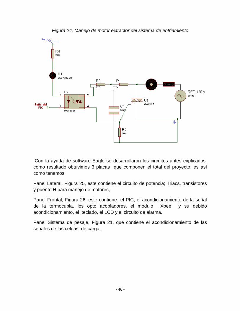
El control del sistema de enfriamiento consta de dos partes, la primera es el
control del motor de apertura y cierre de paso del aire y el segundo es el control
del encendido y apagado del extractor.
Para la primera parte se utilizó un puente H gobernado por dos señales de control
que provienen del micro controlador. Para la segunda se utilizó un motor
monofásico. Una salida del micro controlador se conecta a un opto acoplador y
luego a un TRIAC de potencia para manejar el motor del extractor al igual que se
hace con el motor del giro del cilindro, como se observa en la Figura 24.
- 46 -
Figura 24. Manejo de motor extractor del sistema de enfriamiento
Con la ayuda de software Eagle se desarrollaron los circuitos antes explicados,
como resultado obtuvimos 3 placas que componen el total del proyecto, es así
como tenemos:
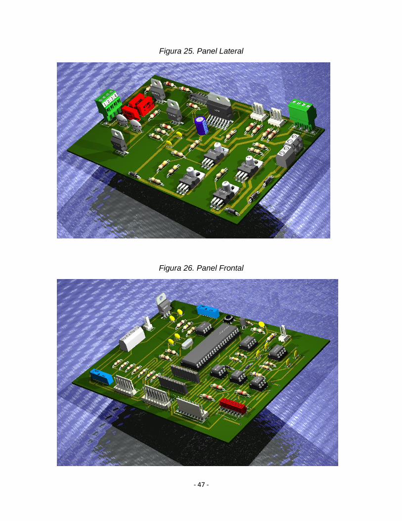
Panel Lateral, Figura 25, este contiene el circuito de potencia; Triacs, transistores
y puente H para manejo de motores,
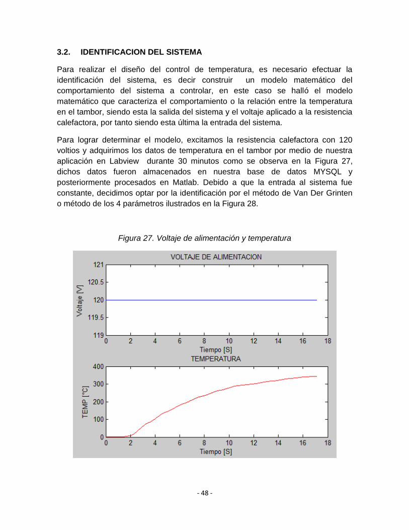
Panel Frontal, Figura 26, este contiene el PIC, el acondicionamiento de la señal
de la termocupla, los opto acopladores, el módulo Xbee y su debido
acondicionamiento, el teclado, el LCD y el circuito de alarma.
Panel Sistema de pesaje, Figura 21, que contiene el acondicionamiento de las
señales de las celdas de carga.
- 47 -
Figura 25. Panel Lateral
Figura 26. Panel Frontal
- 48 -
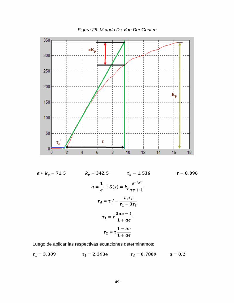
3.2. IDENTIFICACION DEL SISTEMA
Para realizar el diseño del control de temperatura, es necesario efectuar la
identificación del sistema, es decir construir un modelo matemático del
comportamiento del sistema a controlar, en este caso se halló el modelo
matemático que caracteriza el comportamiento o la relación entre la temperatura
en el tambor, siendo esta la salida del sistema y el voltaje aplicado a la resistencia
calefactora, por tanto siendo esta última la entrada del sistema.
Para lograr determinar el modelo, excitamos la resistencia calefactora con 120
voltios y adquirimos los datos de temperatura en el tambor por medio de nuestra
aplicación en Labview durante 30 minutos como se observa en la Figura 27,
dichos datos fueron almacenados en nuestra base de datos MYSQL y
posteriormente procesados en Matlab. Debido a que la entrada al sistema fue
constante, decidimos optar por la identificación por el método de Van Der Grinten
o método de los 4 parámetros ilustrados en la Figura 28.
Figura 27. Voltaje de alimentación y temperatura
- 49 -
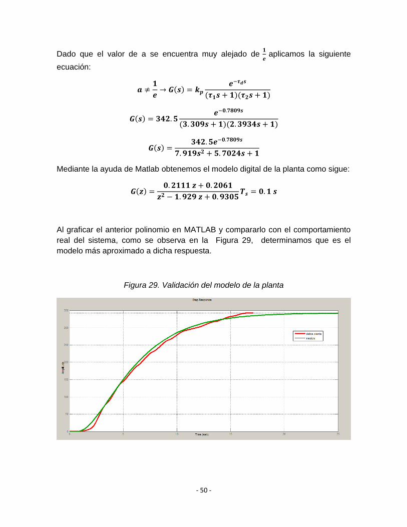
Figura 28. Método De Van Der Grinten
Luego de aplicar las respectivas ecuaciones determinamos:
- 50 -
Dado que el valor de a se encuentra muy alejado de
aplicamos la siguiente
ecuación:
Mediante la ayuda de Matlab obtenemos el modelo digital de la planta como sigue:
Al graficar el anterior polinomio en MATLAB y compararlo con el comportamiento
real del sistema, como se observa en la Figura 29, determinamos que es el
modelo más aproximado a dicha respuesta.
Figura 29. Validación del modelo de la planta
- 51 -
3.3. CONTROL DE TEMPERATURA
Debido a que la temperatura es la variable que define el proceso, el control se
enfoca hacia esta variable. Posteriormente, mediante la ayuda de Matlab
observamos el comportamiento de la planta con realimentación unitaria, con el fin
de determinar qué tipo de control aplicar, es así, como se optó por implementar
un controlador PID, debido a que el sistema realimentado presentaba inestabilidad
y un error muy grande además de que queremos mejorar el tiempo de respuesta,
con esto logramos mejorar el error actual, corregir proporcionalmente la integral
del error, es decir asegurar que aplicando un esfuerzo de control suficiente, el
error de seguimiento se reduce a cero, además de mejorar la reacción del tiempo
en el que el error se produce.
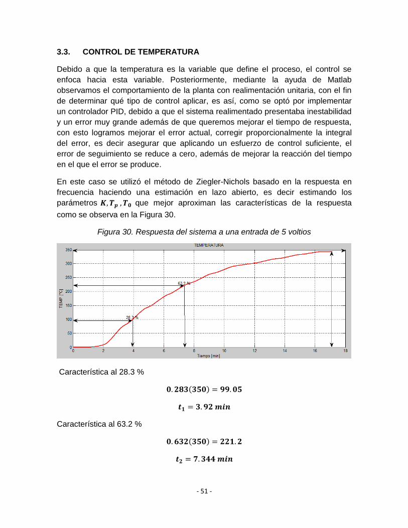
En este caso se utilizó el método de Ziegler-Nichols basado en la respuesta en
frecuencia haciendo una estimación en lazo abierto, es decir estimando los
parámetros que mejor aproximan las características de la respuesta
como se observa en la Figura 30.
Figura 30. Respuesta del sistema a una entrada de 5 voltios
Característica al 28.3 %
Característica al 63.2 %
- 52 -
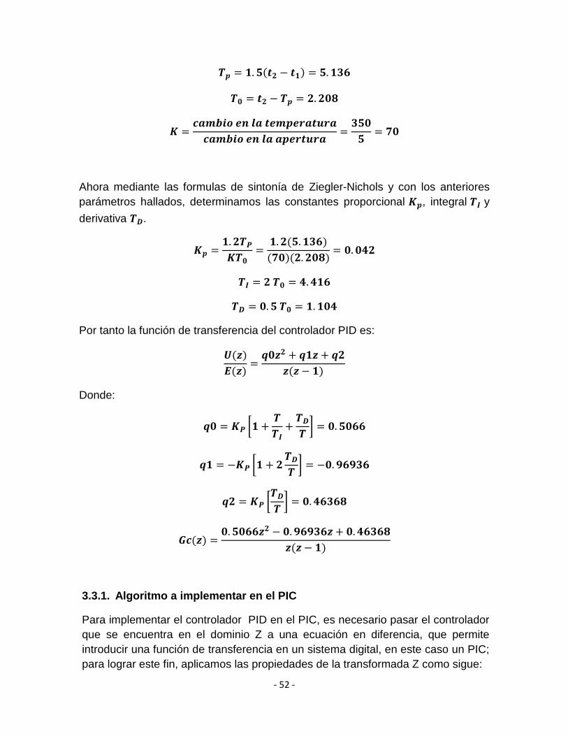
Ahora mediante las formulas de sintonía de Ziegler-Nichols y con los anteriores
parámetros hallados, determinamos las constantes proporcional , integral y
derivativa .
Por tanto la función de transferencia del controlador PID es:
Donde:
[
]
[
]
[
]
3.3.1. Algoritmo a implementar en el PIC
Para implementar el controlador PID en el PIC, es necesario pasar el controlador
que se encuentra en el dominio Z a una ecuación en diferencia, que permite
introducir una función de transferencia en un sistema digital, en este caso un PIC;
para lograr este fin, aplicamos las propiedades de la transformada Z como sigue:
- 53 -
En el PIC, tenemos:
// TempRef: temperatura deseada (introducida por teclado) // TempReal: temperatura sensada en el cilindro tostador eT=TempRef-TempReal; //Cálculo del error uT=q0*eT_1+q2*eT_2+uT_1; //ecuación en diferencia // Guardar variables para próximo estado eT_2=eT_1; eT-1=eT; uT_1=uT;
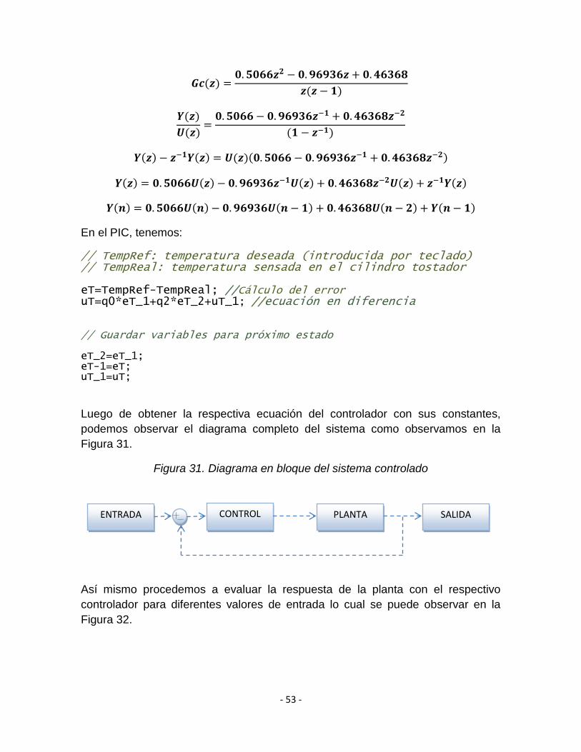
Luego de obtener la respectiva ecuación del controlador con sus constantes,
podemos observar el diagrama completo del sistema como observamos en la
Figura 31.
Figura 31. Diagrama en bloque del sistema controlado
Así mismo procedemos a evaluar la respuesta de la planta con el respectivo
controlador para diferentes valores de entrada lo cual se puede observar en la
Figura 32.
ENTRADA CONTROL PLANTA SALIDA
- 54 -
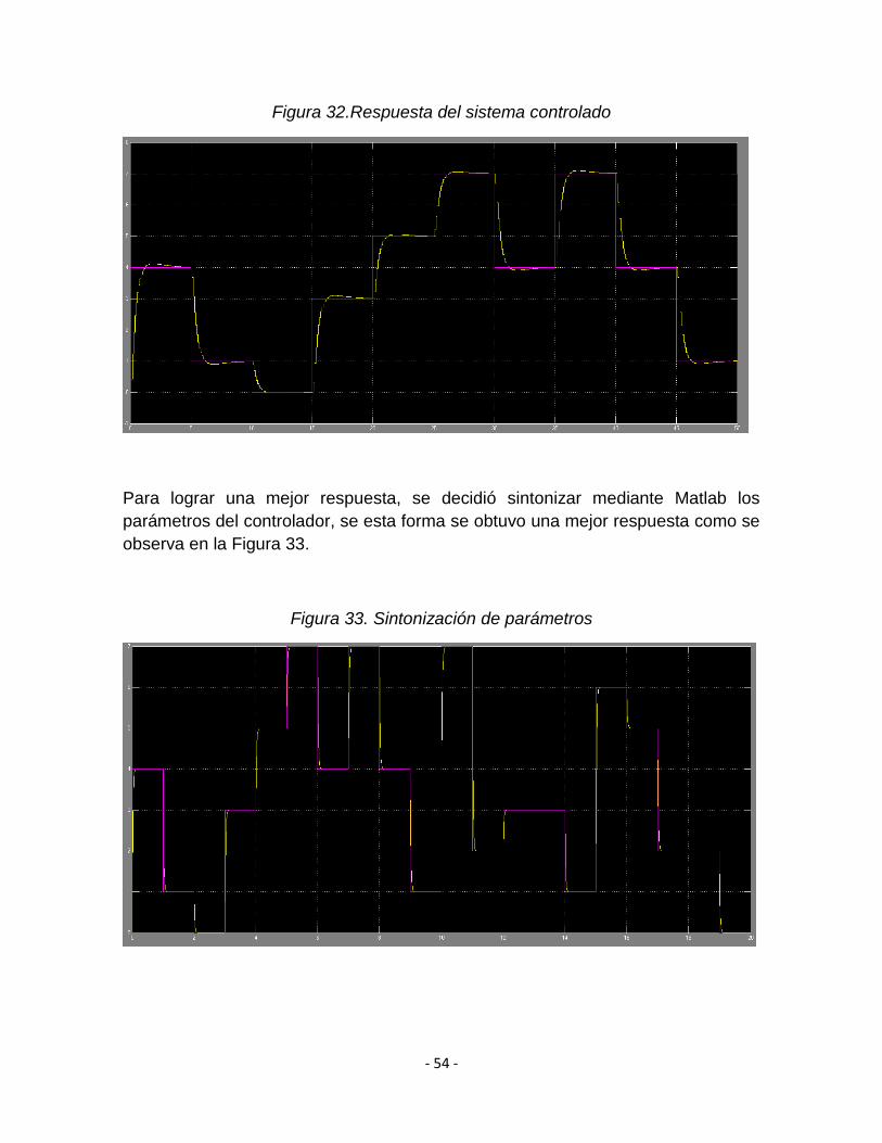
Figura 32.Respuesta del sistema controlado
Para lograr una mejor respuesta, se decidió sintonizar mediante Matlab los
parámetros del controlador, se esta forma se obtuvo una mejor respuesta como se
observa en la Figura 33.
Figura 33. Sintonización de parámetros
- 55 -
3.4. CONTROL DE FASE
El control de fase consistió en hacer que la resistencia calefactora alimentada con
corriente alterna, es decir la señal de 60 Hz a 120 voltios, en lugar de recibir todo
el ciclo senoidal de la tensión de la red, reciba solo parte. Para lograr esto se
dispone la resistencia calefactora en serie con un semiconductor capaz de
conducir la corriente alterna (Triac), como se observa en la Figura 36. Para lograr
el control, se monitorea la señal de cruce por cero y se carga un valor de tiempo
en el PIC, como los tiempos equivalen a ángulos en la corriente alterna, y la
diferencia entre ellos se llama ángulo de fase, al controlar el ángulo en que se
pone a conducir el semiconductor, se controla la tensión que llega a la resistencia,
todo esto con el fin de que en el momento indicado el Triac se dispare y empiece a
conducir solo la tensión necesaria hasta el siguiente cruce por cero, haciendo que
el proceso se repita cada semi-ciclo.
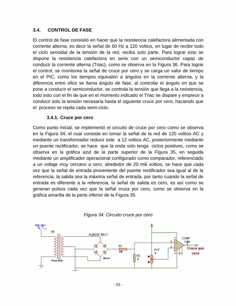
3.4.1. Cruce por cero
Como punto inicial, se implementó el circuito de cruce por cero como se observa
en la Figura 34, el cual consiste en tomar la señal de la red de 120 voltios AC y
mediante un transformador reducir este a 12 voltios AC, posteriormente mediante
un puente rectificador, se hace que la onda solo tenga ciclos positivos, como se
observa en la gráfica azul de la parte superior de la Figura 35, en seguida
mediante un amplificador operacional configurado como comparador, referenciado
a un voltaje muy cercano a cero, alrededor de 20 mili voltios, se hace que cada
vez que la señal de entrada proveniente del puente rectificador sea igual al de la
referencia, la salida sea la máxima señal de entrada, por tanto cuando la señal de
entrada es diferente a la referencia, la señal de salida es cero, es así como se
generan pulsos cada vez que la señal cruza por cero, como se observa en la
gráfica amarilla de la parte inferior de la Figura 35.
Figura 34. Circuito cruce por cero
- 56 -
Figura 35. Gráficas señal rectificada y cruce por cero
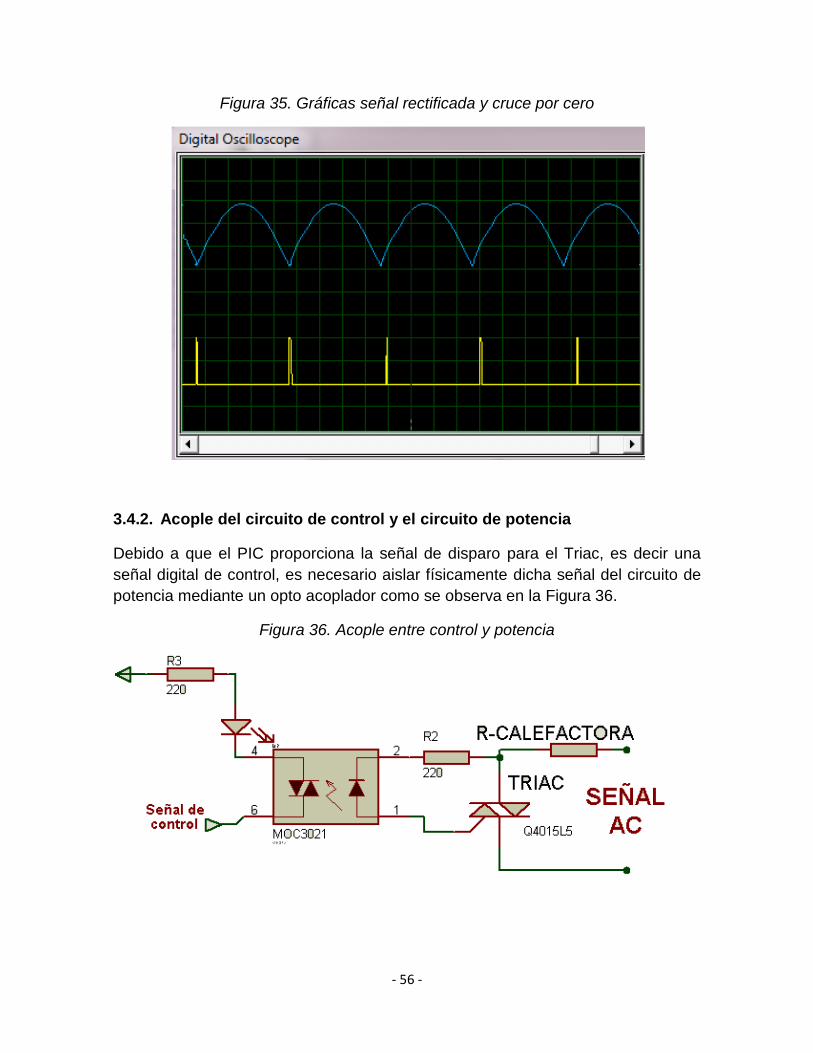
3.4.2. Acople del circuito de control y el circuito de potencia
Debido a que el PIC proporciona la señal de disparo para el Triac, es decir una
señal digital de control, es necesario aislar físicamente dicha señal del circuito de
potencia mediante un opto acoplador como se observa en la Figura 36.
Figura 36. Acople entre control y potencia
- 57 -
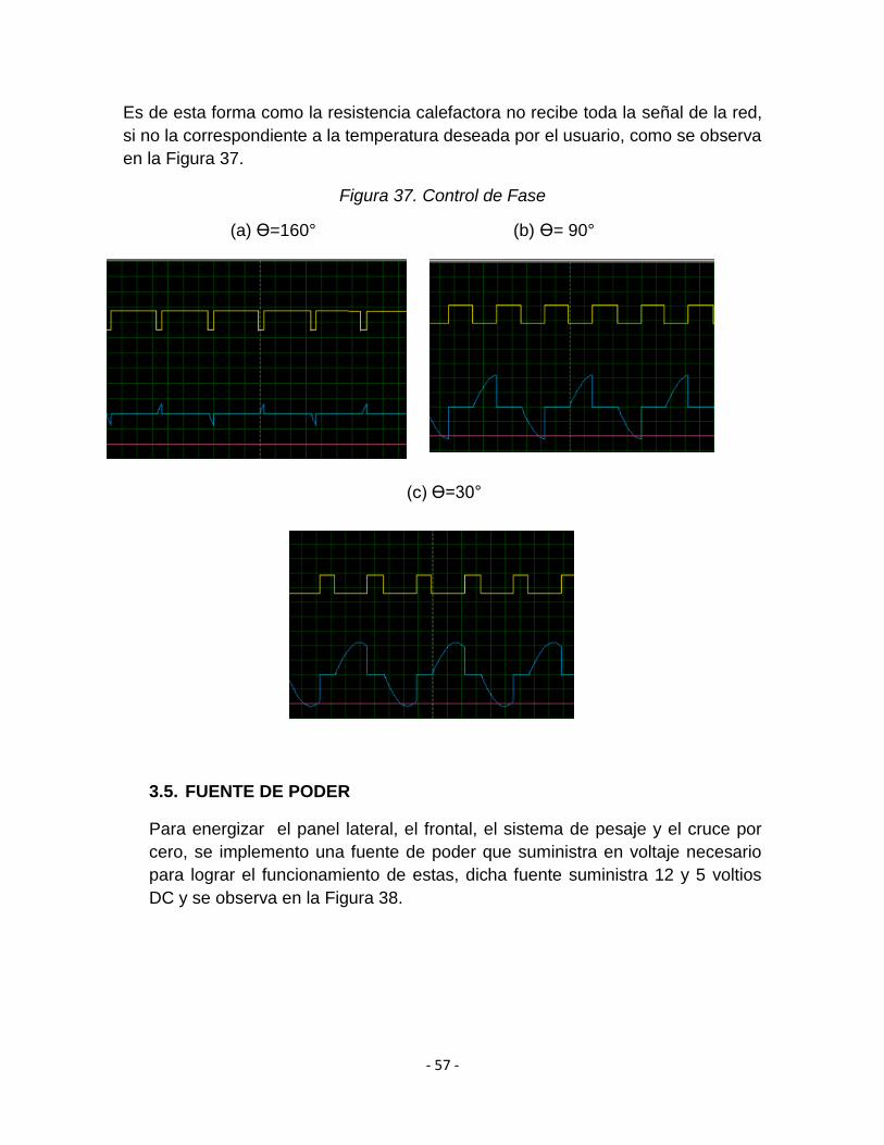
Es de esta forma como la resistencia calefactora no recibe toda la señal de la red,
si no la correspondiente a la temperatura deseada por el usuario, como se observa
en la Figura 37.
Figura 37. Control de Fase
(a) Ө=160° (b) Ө= 90°
(c) Ө=30°
3.5. FUENTE DE PODER
Para energizar el panel lateral, el frontal, el sistema de pesaje y el cruce por
cero, se implemento una fuente de poder que suministra en voltaje necesario
para lograr el funcionamiento de estas, dicha fuente suministra 12 y 5 voltios
DC y se observa en la Figura 38.
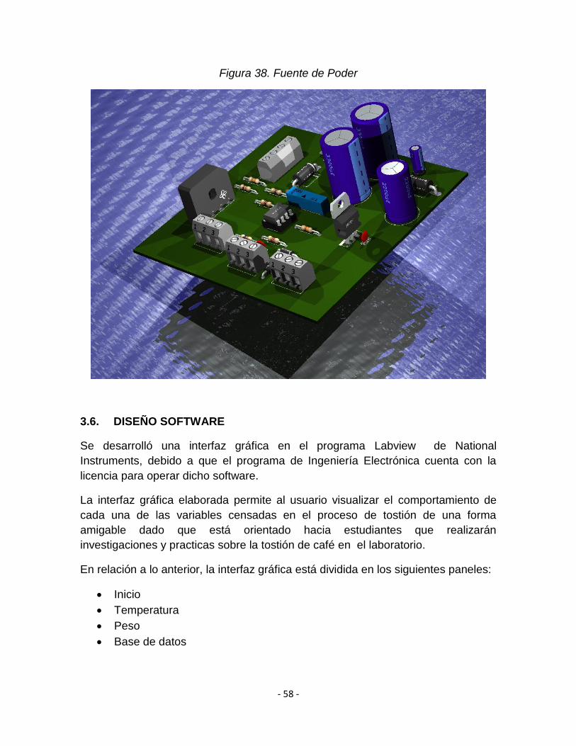
- 58 -
Figura 38. Fuente de Poder
3.6. DISEÑO SOFTWARE
Se desarrolló una interfaz gráfica en el programa Labview de National
Instruments, debido a que el programa de Ingeniería Electrónica cuenta con la
licencia para operar dicho software.
La interfaz gráfica elaborada permite al usuario visualizar el comportamiento de
cada una de las variables censadas en el proceso de tostión de una forma
amigable dado que está orientado hacia estudiantes que realizarán
investigaciones y practicas sobre la tostión de café en el laboratorio.
En relación a lo anterior, la interfaz gráfica está dividida en los siguientes paneles:
Inicio
Temperatura
Peso
Base de datos
- 59 -
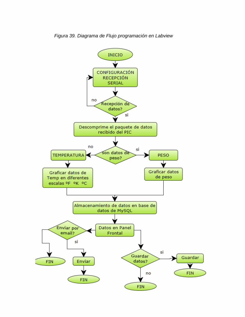
Figura 39. Diagrama de Flujo programación en Labview
- 60 -
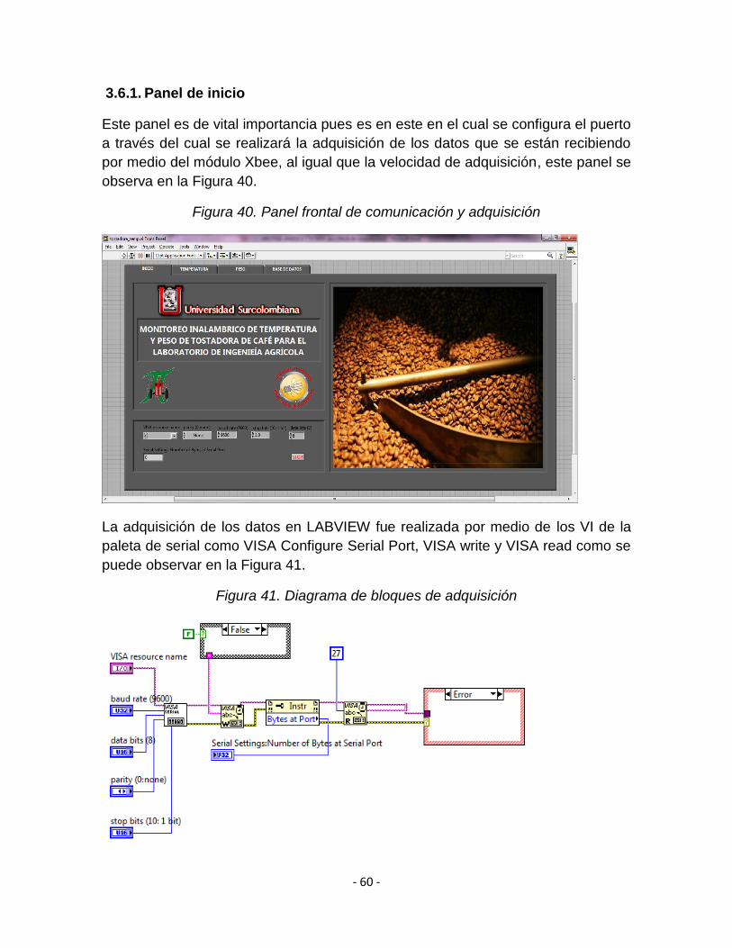
3.6.1. Panel de inicio
Este panel es de vital importancia pues es en este en el cual se configura el puerto
a través del cual se realizará la adquisición de los datos que se están recibiendo
por medio del módulo Xbee, al igual que la velocidad de adquisición, este panel se
observa en la Figura 40.
Figura 40. Panel frontal de comunicación y adquisición
La adquisición de los datos en LABVIEW fue realizada por medio de los VI de la
paleta de serial como VISA Configure Serial Port, VISA write y VISA read como se
puede observar en la Figura 41.
Figura 41. Diagrama de bloques de adquisición
- 61 -
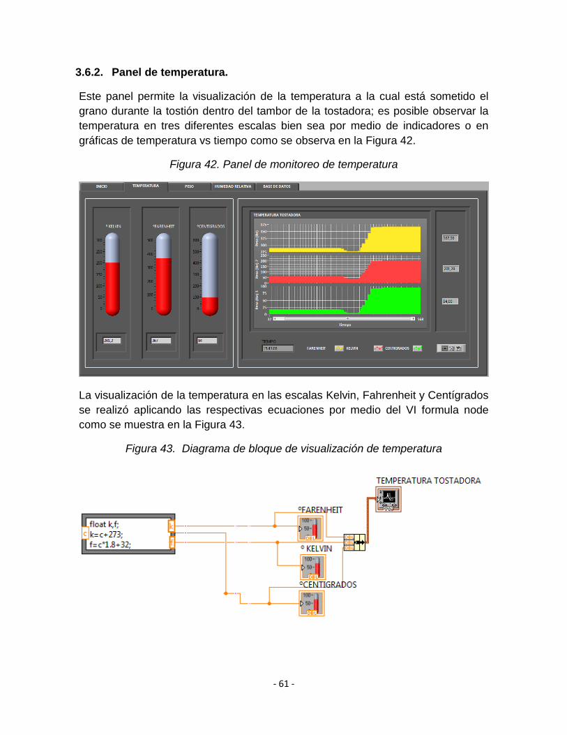
3.6.2. Panel de temperatura.
Este panel permite la visualización de la temperatura a la cual está sometido el
grano durante la tostión dentro del tambor de la tostadora; es posible observar la
temperatura en tres diferentes escalas bien sea por medio de indicadores o en
gráficas de temperatura vs tiempo como se observa en la Figura 42.
Figura 42. Panel de monitoreo de temperatura
La visualización de la temperatura en las escalas Kelvin, Fahrenheit y Centígrados
se realizó aplicando las respectivas ecuaciones por medio del VI formula node
como se muestra en la Figura 43.
Figura 43. Diagrama de bloque de visualización de temperatura
- 62 -
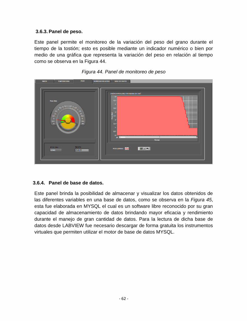
3.6.3. Panel de peso.
Este panel permite el monitoreo de la variación del peso del grano durante el
tiempo de la tostión; esto es posible mediante un indicador numérico o bien por
medio de una gráfica que representa la variación del peso en relación al tiempo
como se observa en la Figura 44.
Figura 44. Panel de monitoreo de peso
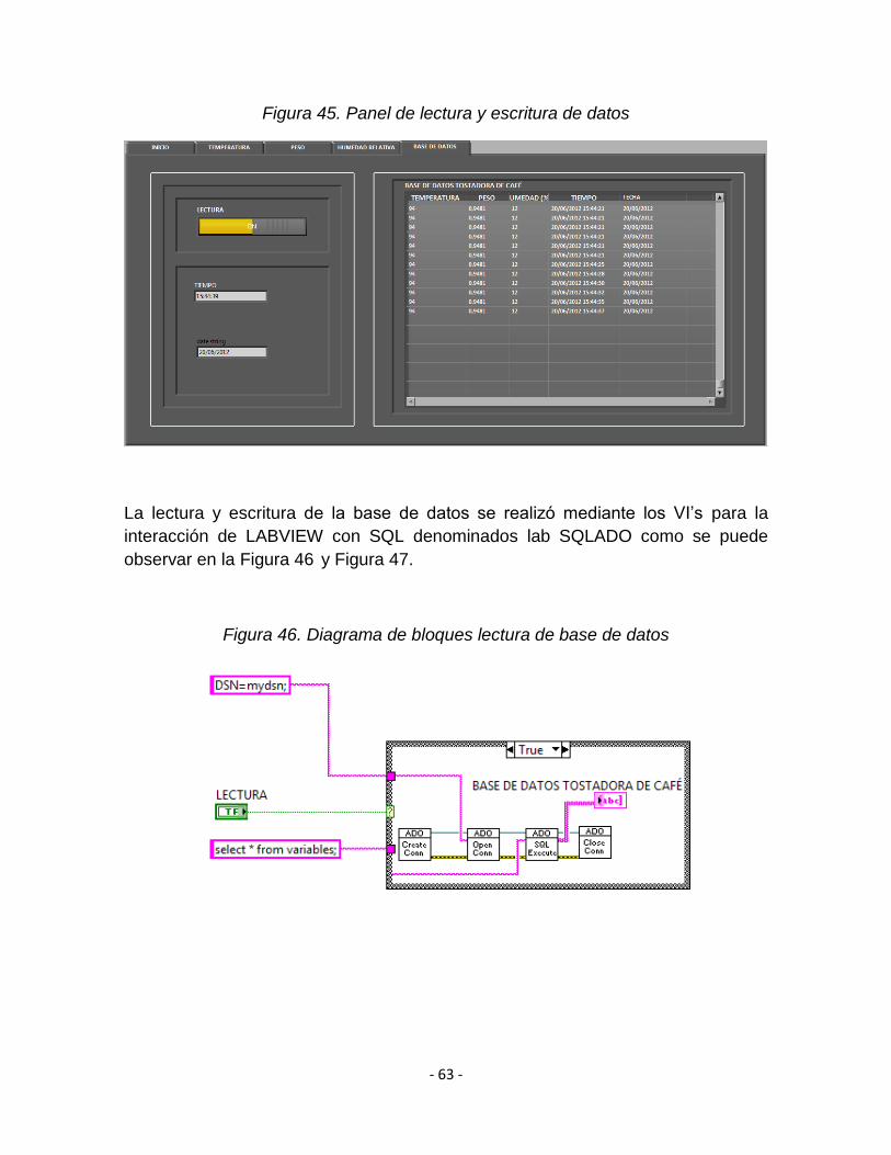
3.6.4. Panel de base de datos.
Este panel brinda la posibilidad de almacenar y visualizar los datos obtenidos de
las diferentes variables en una base de datos, como se observa en la Figura 45,
esta fue elaborada en MYSQL el cual es un software libre reconocido por su gran
capacidad de almacenamiento de datos brindando mayor eficacia y rendimiento
durante el manejo de gran cantidad de datos. Para la lectura de dicha base de
datos desde LABVIEW fue necesario descargar de forma gratuita los instrumentos
virtuales que permiten utilizar el motor de base de datos MYSQL.
- 63 -
Figura 45. Panel de lectura y escritura de datos
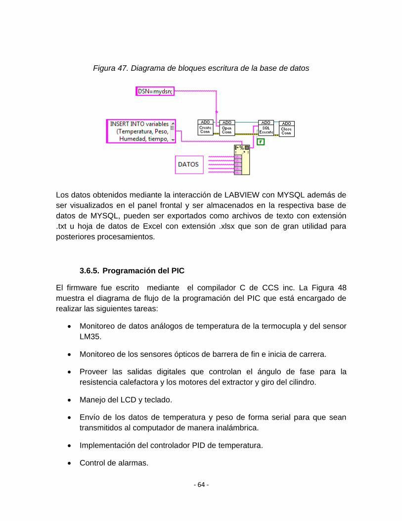
La lectura y escritura de la base de datos se realizó mediante los VI’s para la
interacción de LABVIEW con SQL denominados lab SQLADO como se puede
observar en la Figura 46 y Figura 47.
Figura 46. Diagrama de bloques lectura de base de datos
- 64 -
Figura 47. Diagrama de bloques escritura de la base de datos
Los datos obtenidos mediante la interacción de LABVIEW con MYSQL además de
ser visualizados en el panel frontal y ser almacenados en la respectiva base de
datos de MYSQL, pueden ser exportados como archivos de texto con extensión
.txt u hoja de datos de Excel con extensión .xlsx que son de gran utilidad para
posteriores procesamientos.
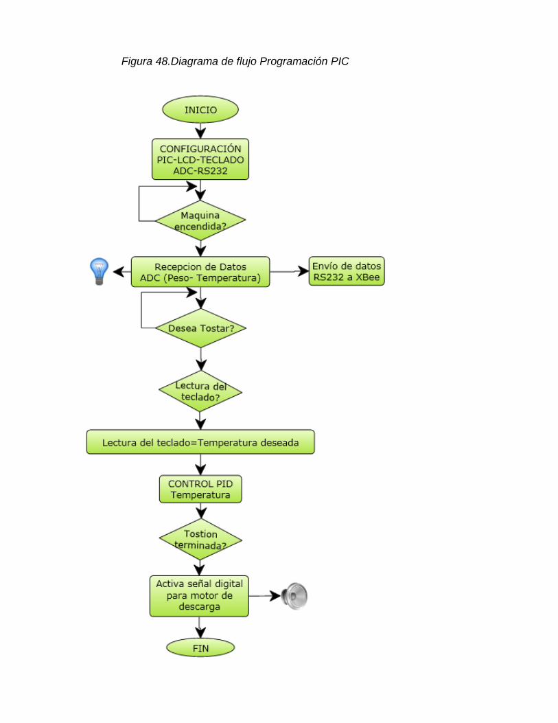
3.6.5. Programación del PIC
El firmware fue escrito mediante el compilador C de CCS inc. La Figura 48
muestra el diagrama de flujo de la programación del PIC que está encargado de
realizar las siguientes tareas:
Monitoreo de datos análogos de temperatura de la termocupla y del sensor
LM35.
Monitoreo de los sensores ópticos de barrera de fin e inicia de carrera.
Proveer las salidas digitales que controlan el ángulo de fase para la
resistencia calefactora y los motores del extractor y giro del cilindro.
Manejo del LCD y teclado.
Envío de los datos de temperatura y peso de forma serial para que sean
transmitidos al computador de manera inalámbrica.
Implementación del controlador PID de temperatura.
Control de alarmas.
- 65 -
Figura 48.Diagrama de flujo Programación PIC
- 66 -
4. CONCLUSIONES
Se diseñó e implementó la automatización de una tostadora de café del
programa de Ingeniería Agrícola de la Universidad Surcolombiana, el cual
consta de un sistema de pesaje, control PID de temperatura y envío
inalámbrico de datos.
La temperatura es la variable más adecuada a controlar en el proceso de
torrefacción de café.
El peso es una variable importante en el proceso de torrefacción, por lo tanto
monitorearla aporta información para la investigación en este sector.
La aplicación desarrollada en Labview permite al usuario acceder de manera
sencilla a los datos que están siendo monitoreados durante el proceso,
mediante gráficas y tablas.
La comunicación inalámbrica implementada por medio de tecnología Zigbee
facilita al usuario el acceso a la máquina y a los datos sin necesidad de
cableado.
- 67 -
5. RECOMENDACIONES
Monitorear otras variables en el proceso de torrefacción, como el color, por
medio de un instrumento que permita medir la reflectancia del color.
Realizar periódicamente revisiones y mantenimiento que sean necesarios para
que la máquina permanezca en buen estado.
Integrar la máquina de torrefacción con el laboratorio de Análisis Sensorial del
Programa de Ingeniería Agrícola de la Universidad Surcolombiana.
- 68 -
BIBLIOGRAFÍA
ARIAN, Control y Automatización. Termocuplas y su funcionamiento. [En línea]
Disponible en: <http://www.arian.cl/downloads/nt-002.pdf>. Consulta: 29 Julio de
2011.
ARIAS, H.; CORREGIDOR, J. Máquinas de torrefacción de café para laboratorios de control de calidad. Colombia, Bogotá. Universidad Distrital Francisco José de Caldas. 4 págs. BELLINI, B. Sensores de presión utilizados en las plataformas de fuerza aplicadas al estudio de la posturografía. Uruguay. Programa Ingeniería Biomédica. Universidad de la República. 10 Págs. COSTE, R. El café. Ed. Blume, 1969. Barcelona. 256 págs.
FEDERACION NACIONAL DE CAFETEROS DE COLOMBIA. Torrefacción o
tostadora de café. En: revista cafetera de Colombia Bogotá. Vol. 4, No 38, (mayo
junio 1932) pág. 1470
FIGEROA, J. módulos de radiofrecuencia XBee/XBee-pro. Ecuador. Escuela
Politécnica del Ejército. Club de Robótica. 95 Págs.
HENAO, Y.H. (2004) Diseño e implementación de una tostadora de café
controlada electrónicamente. Colombia. Programa de Ingeniería Electrónica.
Universidad Surcolombiana. 210 págs.
GÓNGORA RUIZ, M.A.; CORTÉS CASTILLO, F. (2010). Automatización de secador
de café (Tipo silo) de laboratorio. Colombia. Programa de Ingeniería Electrónica.
Universidad Surcolombiana. 111 págs.
HERRERA, N.E. (1999) La torrefacción rápida (High Yield), sus principales
características y su aplicabilidad en la industria cafetera. Colombia, Bogotá: Tesis
Ingeniería de alimentos, Universidad de la Salle, P.20-21
LA TORREFACCIÓN DEL CAFÉ. . [En línea] Disponible en: <http://academic.uprm.edu/mmonroig/id49.htm>. Consulta: 29 Julio de 2011. LOPEZ, E.M. (1998) Extracción de aceite esencial a partir del café brocado.
Colombia, Manizales: Tesis Ingeniería Química, Universidad Nacional de
Colombia, 256 págs.
MAYNÉ, J. IEEE 802.15.4 y ZigBee. España, Cataluña. ZigBee Alliance. P: 14.
- 69 -
PRIETO, Y.A. Caracterización Física Del Café Semitostado. Colombia, Bogotá. Tesis Fundación Universitaria De América. P: 14-27. RONCANCIO, H.A.; CIFUENTES, H. Tutorial de LABVIEW. Universidad Distrital Francisco José de Caldas. Laboratorio de Electrónica. 100 Págs.
TIMMOTHY J.G. The Craft of Espresso Roasting. Tea & Coffee - July/August,
2004. Disponible en Web: <http://www.teaandcoffee.net/0704/coffee.htm>.
Consulta: 29 Julio de 2012.
- 70 -
ANEXOS
ANEXO A. PROGRAMACIÓN PIC
Este anexo se encuentra en el CD que acompaña este libro.
ANEXO B. MÓDULOS INALÁMBRICOS XBEE
Este anexo se encuentra en el CD que acompaña este libro.
ANEXO C. COEFICIENTES DE POLINOMIOS DE NIST
Este anexo se encuentra en el CD que acompaña este libro.
ANEXO D. CELDA DE CARGA MONOBLOQUE SP06
Este anexo se encuentra en el CD que acompaña este libro.
ANEXO E. AMPLIFICADOR DE INSTRUMENTACIÓN AD620
Este anexo se encuentra en el CD que acompaña este libro.
ANEXO F. REGULADOR DE VOLTAJE LM317
Este anexo se encuentra en el CD que acompaña este libro.
ANEXO G. AMPLIFICADOR OPERACIONAL TL084
Este anexo se encuentra en el CD que acompaña este libro.
ANEXO H. PROGRAMACIÓN EN LAVIEW
Este anexo se encuentra en el CD que acompaña este libro
Automatización de Máquina de Torrefacción de Café para el
Laboratorio del Programa de Ingeniería Agrícola de la
Universidad Surcolombiana
Automation of a Coffee Roaster Machine of Agricultural
Engineering Laboratory at Surcolombiana University
Agustín Soto Otalora1, Angélica María Cárdenas Castaño
2, Jenifer Tatiana Osorio
Guzmán3
Resumen
Este trabajo consiste en el control y la automatización de una máquina de torrefacción de laboratorio del
programa de Ingeniería Agrícola de la Universidad Surcolombiana, la cual fue dotada con celdas de carga y los
arreglos adecuados al sensor de temperatura con el fin de hacer su control, por tanto se monitorean variables
tales como peso y temperatura de manera inalámbrica desde el computador por medio del software LabVIEW e
igualmente se tiene la opción de visualizar dicho monitoreo desde el LCD ubicado en la máquina. Para el
desarrollo de este proyecto fue fundamental conocer completamente el proceso de torrefacción, además de las
características de todos los sensores y dispositivos usados en esta, con el fin de obtener medidas precisas,
además de un control óptimo. Como resultado de este trabajo, se obtuvo una tostadora controlada por
temperatura, con monitoreo del peso, con visualización de estas variables tanto en un LCD como en una
aplicación en LabVIEW que me permite, visualizar, controlar y almacenar todos los cambios que sufre el café en
relación a su peso y temperatura durante el proceso de torrefacción.
Palabras Claves: Control, automatización, torrefacción, LabVIEW.
Abstract
This work is about the control and automation of a coffee roaster machine of Agricultural Engineering
laboratory at Surcolombiana University, which was outfitted by load cells and some modifications to sensor
temperature with the purpose of making its control, also were monitored every variables wirelessly through
LabVIEW software on the computer, furthermore offers the option of visualizing the monitoring on the LCD that
is in the machine. For the development of this project was essential to know fully the roaster process, also the
characteristics of each sensor and device which was used in this machine, for the purpose of acquiring accurate
measurements and an optimum control.
As result of this work, we obtain a roast which was controlled by temperature, with monitoring of weight,
with visualization of these variables on a LCD. We develop an application on LabVIEW which offers the
possibility of visualizing, controlling and saving all changes that the coffee is suffering relation to its weight and
temperature during the roast process.
Keywords: LabView, ZigBee, Fuzzy control, humidity, temperature.
1 Ingeniero Electrónico. Universidad Surcolombiana. Neiva Av. Pastrana Borrero – Carrera 1. [email protected]
2 Ingeniero Electrónico. Universidad Surcolombiana. Neiva Av. Pastrana Borrero – Carrera 1. [email protected]
3 Ingeniero Electrónico. Universidad Surcolombiana. Neiva Av. Pastrana Borrero – Carrera 1. [email protected]
1. Introducción
Colombia hace parte de los principales productores de café verde en el mundo siendo su producción y
comercialización una de las principales fuentes de ingresos para el país, es por ello que es de gran importancia la
investigación que se realiza actualmente en este campo con el fin de obtener un café de mejores características
constituyéndolo así, como un producto de alta calidad.
Es necesario tener en cuenta que la investigación realizada en el sector cafetero tiene como objetivo la
obtención de una mejor materia prima y así mismo de un mejor café como producto final luego de múltiples
procesos realizados con el fin de explotar al máximo sus características de sabor, aroma, color y textura.
Actualmente el programa de Ingeniería Agrícola de la Universidad Surcolombiana realiza investigaciones en
relación al procesamiento del café, siendo de gran importancia para la región, dado que el departamento del
Huila en los últimos años ha mostrado gran avance en cuanto a producción de cafés especiales, catalogándose
hoy en día como el primer productor de estos en el país, según el Comité Nacional de Cafeteros de Colombia.
Es preciso destacar la importante labor realizada por el Programa de Ingeniería Agrícola, el cual a través de
los años ha avanzado en sus investigaciones en el sector cafetero gracias a la adquisición de maquinaria
apropiada para los diferentes procesos realizados al grano como son fermentación, secado y torrefacción.
Aunque el Programa ya contaba con una máquina de torrefacción de café diseñada e implementada por un
estudiante del programa de Ingeniería Electrónica de la universidad Surcolombiana en el año 2004, la cual
contaba con un sistema de control de temperatura On-Off por medio de una termocupla y un sistema de
descarga y enfriamiento; lo que se desarrolla en esta tesis es el mejoramiento de dicho sistema de control ,
además de monitorear el peso y la temperatura del grano de manera inalámbrica y su posterior visualización en
el software LabVIEW.
En relación a lo anterior, el desarrollo de este trabajo hace un aporte importante a la investigación de este
proceso en el sector cafetero, puesto que permite a los investigadores acceder de una manera más fácil a los
datos relacionados con el proceso, con el fin de observar la dinámica de estas y determinar posteriormente
algunas características que permitirán aportar en el mejoramiento de la producción del café como materia final.
2. Metodología
En El sistema propuesto para esta aplicación consta de varios módulos que pueden ser apreciados en el
diagrama de bloques que se muestra en la figura 1.
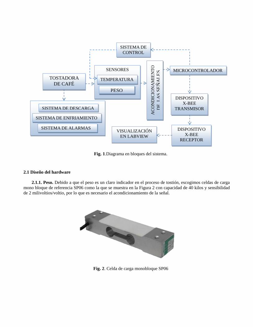
Fig. 1.Diagrama en bloques del sistema.
2.1 Diseño del hardware
2.1.1. Peso. Debido a que el peso es un claro indicador en el proceso de tostión, escogimos celdas de carga
mono bloque de referencia SP06 como la que se muestra en la Figura 2 con capacidad de 40 kilos y sensibilidad
de 2 milivoltios/voltio, por lo que es necesario el acondicionamiento de la señal.
Fig. 2. Celda de carga monobloque SP06
SENSORES
SISTEMA DE DESCARGA
SISTEMA DE ENFRIAMIENTO
SISTEMA DE ALARMAS
SISTEMA DE
CONTROL
TOSTADORA
DE CAFÉ
AC
ON
DIC
ION
AM
IEN
TO
DE
L
AS
SE
ÑA
LE
S MICROCONTROLADOR
DISPOSITIVO
X-BEE TRANSMISOR
DISPOSITIVO
X-BEE
RECEPTOR
VISUALIZACIÓN
EN LABVIEW
TEMPERATURA
PESO
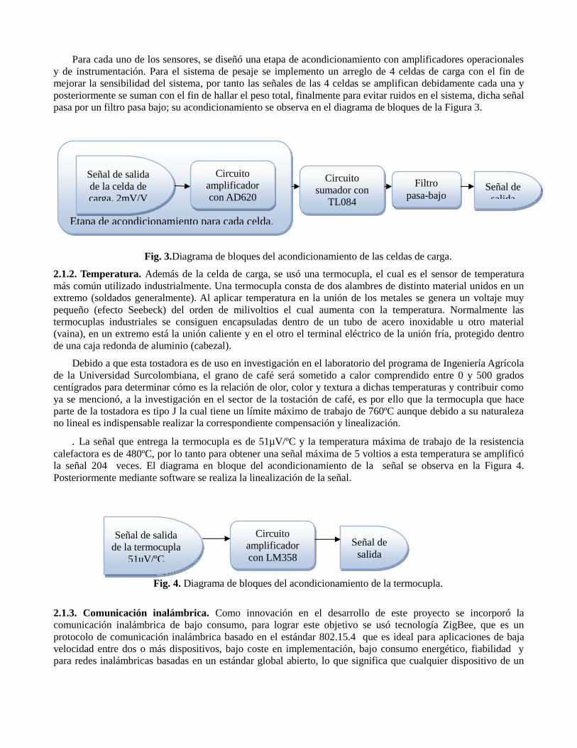
Para cada uno de los sensores, se diseñó una etapa de acondicionamiento con amplificadores operacionales
y de instrumentación. Para el sistema de pesaje se implemento un arreglo de 4 celdas de carga con el fin de
mejorar la sensibilidad del sistema, por tanto las señales de las 4 celdas se amplifican debidamente cada una y
posteriormente se suman con el fin de hallar el peso total, finalmente para evitar ruidos en el sistema, dicha señal
pasa por un filtro pasa bajo; su acondicionamiento se observa en el diagrama de bloques de la Figura 3.
Fig. 3.Diagrama de bloques del acondicionamiento de las celdas de carga.
2.1.2. Temperatura. Además de la celda de carga, se usó una termocupla, el cual es el sensor de temperatura
más común utilizado industrialmente. Una termocupla consta de dos alambres de distinto material unidos en un
extremo (soldados generalmente). Al aplicar temperatura en la unión de los metales se genera un voltaje muy
pequeño (efecto Seebeck) del orden de milivoltios el cual aumenta con la temperatura. Normalmente las
termocuplas industriales se consiguen encapsuladas dentro de un tubo de acero inoxidable u otro material
(vaina), en un extremo está la unión caliente y en el otro el terminal eléctrico de la unión fría, protegido dentro
de una caja redonda de aluminio (cabezal).
Debido a que esta tostadora es de uso en investigación en el laboratorio del programa de Ingeniería Agrícola
de la Universidad Surcolombiana, el grano de café será sometido a calor comprendido entre 0 y 500 grados
centígrados para determinar cómo es la relación de olor, color y textura a dichas temperaturas y contribuir como
ya se mencionó, a la investigación en el sector de la tostación de café, es por ello que la termocupla que hace
parte de la tostadora es tipo J la cual tiene un límite máximo de trabajo de 760ºC aunque debido a su naturaleza
no lineal es indispensable realizar la correspondiente compensación y linealización.
. La señal que entrega la termocupla es de 51µV/ºC y la temperatura máxima de trabajo de la resistencia
calefactora es de 480ºC, por lo tanto para obtener una señal máxima de 5 voltios a esta temperatura se amplificó
la señal 204 veces. El diagrama en bloque del acondicionamiento de la señal se observa en la Figura 4.
Posteriormente mediante software se realiza la linealización de la señal.
Fig. 4. Diagrama de bloques del acondicionamiento de la termocupla.
2.1.3. Comunicación inalámbrica. Como innovación en el desarrollo de este proyecto se incorporó la
comunicación inalámbrica de bajo consumo, para lograr este objetivo se usó tecnología ZigBee, que es un
protocolo de comunicación inalámbrica basado en el estándar 802.15.4 que es ideal para aplicaciones de baja
velocidad entre dos o más dispositivos, bajo coste en implementación, bajo consumo energético, fiabilidad y
para redes inalámbricas basadas en un estándar global abierto, lo que significa que cualquier dispositivo de un
Etapa de acondicionamiento para cada celda.
Circuito
amplificador
con AD620
Señal de salida
de la celda de
carga, 2mV/V
Circuito
sumador con
TL084
Filtro
pasa-bajo Señal de
salida
Señal de salida
de la termocupla
51uV/ºC
Circuito
amplificador
con LM358
Señal de
salida
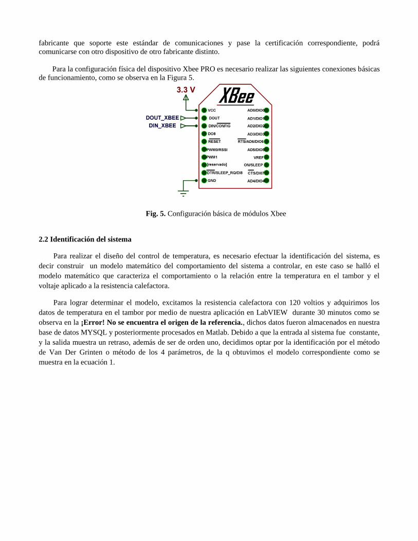
fabricante que soporte este estándar de comunicaciones y pase la certificación correspondiente, podrá
comunicarse con otro dispositivo de otro fabricante distinto.
Para la configuración física del dispositivo Xbee PRO es necesario realizar las siguientes conexiones básicas
de funcionamiento, como se observa en la Figura 5.
Fig. 5. Configuración básica de módulos Xbee
2.2 Identificación del sistema
Para realizar el diseño del control de temperatura, es necesario efectuar la identificación del sistema, es
decir construir un modelo matemático del comportamiento del sistema a controlar, en este caso se halló el
modelo matemático que caracteriza el comportamiento o la relación entre la temperatura en el tambor y el
voltaje aplicado a la resistencia calefactora.
Para lograr determinar el modelo, excitamos la resistencia calefactora con 120 voltios y adquirimos los
datos de temperatura en el tambor por medio de nuestra aplicación en LabVIEW durante 30 minutos como se
observa en la ¡Error! No se encuentra el origen de la referencia., dichos datos fueron almacenados en nuestra
base de datos MYSQL y posteriormente procesados en Matlab. Debido a que la entrada al sistema fue constante,
y la salida muestra un retraso, además de ser de orden uno, decidimos optar por la identificación por el método
de Van Der Grinten o método de los 4 parámetros, de la q obtuvimos el modelo correspondiente como se
muestra en la ecuación 1.
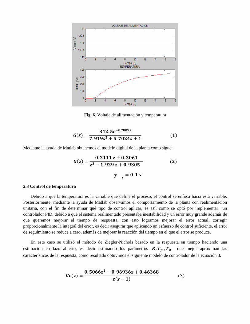
Fig. 6. Voltaje de alimentación y temperatura
( )
( )
Mediante la ayuda de Matlab obtenemos el modelo digital de la planta como sigue:
( )
( )
2.3 Control de temperatura
Debido a que la temperatura es la variable que define el proceso, el control se enfoca hacia esta variable.
Posteriormente, mediante la ayuda de Matlab observamos el comportamiento de la planta con realimentación
unitaria, con el fin de determinar qué tipo de control aplicar, es así, como se optó por implementar un
controlador PID, debido a que el sistema realimentado presentaba inestabilidad y un error muy grande además de
que queremos mejorar el tiempo de respuesta, con esto logramos mejorar el error actual, corregir
proporcionalmente la integral del error, es decir asegurar que aplicando un esfuerzo de control suficiente, el error
de seguimiento se reduce a cero, además de mejorar la reacción del tiempo en el que el error se produce.
En este caso se utilizó el método de Ziegler-Nichols basado en la respuesta en tiempo haciendo una
estimación en lazo abierto, es decir estimando los parámetros que mejor aproximan las
características de la respuesta, como resultado obtuvimos el siguiente modelo de controlador de la ecuación 3.
( )
( ) ( )
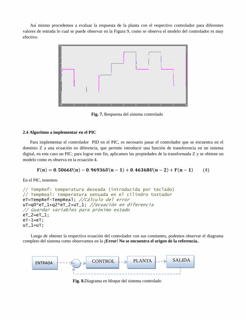
Así mismo procedemos a evaluar la respuesta de la planta con el respectivo controlador para diferentes
valores de entrada lo cual se puede observar en la Figura 9, como se observa el modelo del controlador es muy
efectivo.
Fig. 7. Respuesta del sistema controlado
2.4 Algoritmo a implementar en el PIC
Para implementar el controlador PID en el PIC, es necesario pasar el controlador que se encuentra en el
dominio Z a una ecuación en diferencia, que permite introducir una función de transferencia en un sistema
digital, en este caso un PIC; para lograr este fin, aplicamos las propiedades de la transformada Z y se obtiene un
modelo como es observa en la ecuación 4.
( ) ( ) ( ) ( ) ( ) ( )
En el PIC, tenemos:
// TempRef: temperatura deseada (introducida por teclado) // TempReal: temperatura sensada en el cilindro tostador eT=TempRef-TempReal; //Cálculo del error uT=q0*eT_1+q2*eT_2+uT_1; //ecuación en diferencia // Guardar variables para próximo estado eT_2=eT_1; eT-1=eT; uT_1=uT;
Luego de obtener la respectiva ecuación del controlador con sus constantes, podemos observar el diagrama
completo del sistema como observamos en la ¡Error! No se encuentra el origen de la referencia..
ENTRADA CONTROL PLANTA SALIDA
Fig. 8.Diagrama en bloque del sistema controlado
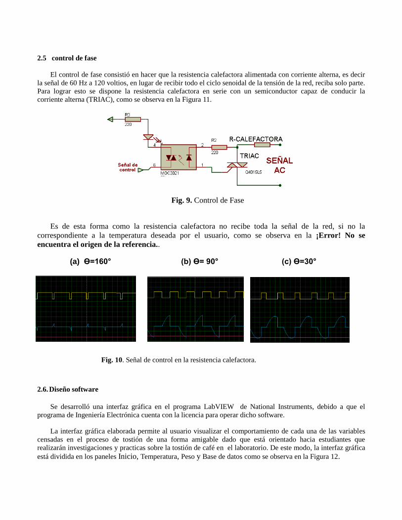
2.5 control de fase
El control de fase consistió en hacer que la resistencia calefactora alimentada con corriente alterna, es decir
la señal de 60 Hz a 120 voltios, en lugar de recibir todo el ciclo senoidal de la tensión de la red, reciba solo parte.
Para lograr esto se dispone la resistencia calefactora en serie con un semiconductor capaz de conducir la
corriente alterna (TRIAC), como se observa en la Figura 11.
Fig. 9. Control de Fase
Es de esta forma como la resistencia calefactora no recibe toda la señal de la red, si no la
correspondiente a la temperatura deseada por el usuario, como se observa en la ¡Error! No se
encuentra el origen de la referencia..
(a) Ө=160° (b) Ө= 90° (c) Ө=30°
2.6. Diseño software
Se desarrolló una interfaz gráfica en el programa LabVIEW de National Instruments, debido a que el
programa de Ingeniería Electrónica cuenta con la licencia para operar dicho software.
La interfaz gráfica elaborada permite al usuario visualizar el comportamiento de cada una de las variables
censadas en el proceso de tostión de una forma amigable dado que está orientado hacia estudiantes que
realizarán investigaciones y practicas sobre la tostión de café en el laboratorio. De este modo, la interfaz gráfica
está dividida en los paneles Inicio, Temperatura, Peso y Base de datos como se observa en la Figura 12.
Fig. 10. Señal de control en la resistencia calefactora.
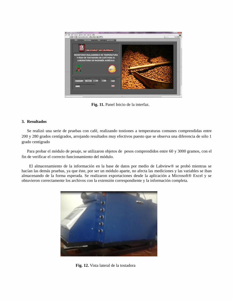
Fig. 11. Panel Inicio de la interfaz.
3. Resultados
Se realizó una serie de pruebas con café, realizando tostiones a temperaturas comunes comprendidas entre
200 y 280 grados centígrados, arrojando resultados muy efectivos puesto que se observa una diferencia de sólo 1
grado centígrado
Para probar el módulo de pesaje, se utilizaron objetos de pesos comprendidos entre 60 y 3000 gramos, con el
fin de verificar el correcto funcionamiento del módulo.
El almacenamiento de la información en la base de datos por medio de Labview® se probó mientras se
hacían las demás pruebas, ya que éste, por ser un módulo aparte, no afecta las mediciones y las variables se iban
almacenando de la forma esperada. Se realizaron exportaciones desde la aplicación a Microsoft® Excel y se
obtuvieron correctamente los archivos con la extensión correspondiente y la información completa.
Fig. 12. Vista lateral de la tostadora
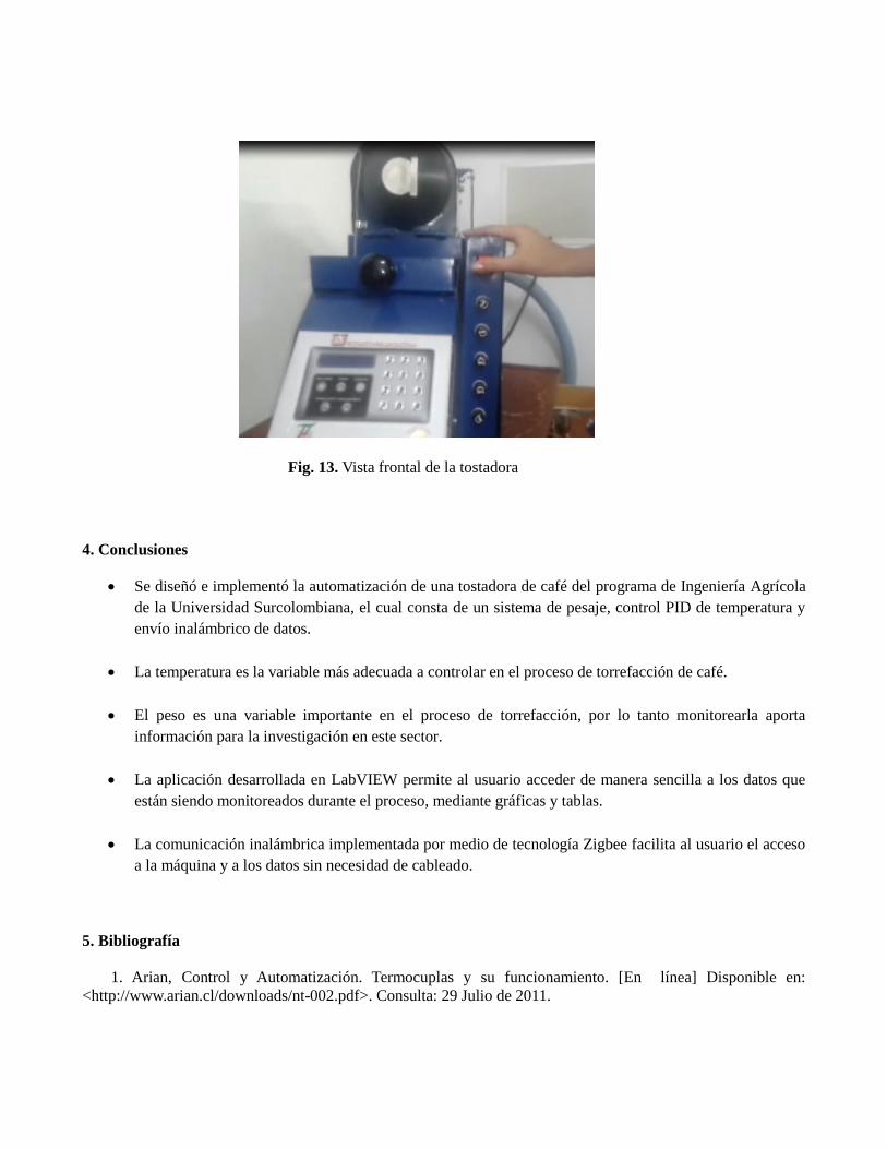
Fig. 13. Vista frontal de la tostadora
4. Conclusiones
Se diseñó e implementó la automatización de una tostadora de café del programa de Ingeniería Agrícola
de la Universidad Surcolombiana, el cual consta de un sistema de pesaje, control PID de temperatura y
envío inalámbrico de datos.
La temperatura es la variable más adecuada a controlar en el proceso de torrefacción de café.
El peso es una variable importante en el proceso de torrefacción, por lo tanto monitorearla aporta
información para la investigación en este sector.
La aplicación desarrollada en LabVIEW permite al usuario acceder de manera sencilla a los datos que
están siendo monitoreados durante el proceso, mediante gráficas y tablas.
La comunicación inalámbrica implementada por medio de tecnología Zigbee facilita al usuario el acceso
a la máquina y a los datos sin necesidad de cableado.
5. Bibliografía
1. Arian, Control y Automatización. Termocuplas y su funcionamiento. [En línea] Disponible en:
<http://www.arian.cl/downloads/nt-002.pdf>. Consulta: 29 Julio de 2011.
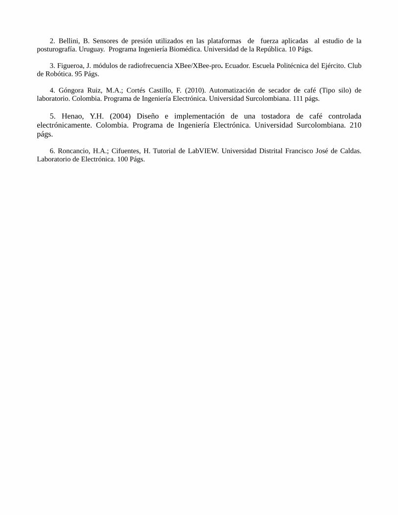
2. Bellini, B. Sensores de presión utilizados en las plataformas de fuerza aplicadas al estudio de la
posturografía. Uruguay. Programa Ingeniería Biomédica. Universidad de la República. 10 Págs.
3. Figueroa, J. módulos de radiofrecuencia XBee/XBee-pro. Ecuador. Escuela Politécnica del Ejército. Club
de Robótica. 95 Págs.
4. Góngora Ruiz, M.A.; Cortés Castillo, F. (2010). Automatización de secador de café (Tipo silo) de
laboratorio. Colombia. Programa de Ingeniería Electrónica. Universidad Surcolombiana. 111 págs.
5. Henao, Y.H. (2004) Diseño e implementación de una tostadora de café controlada
electrónicamente. Colombia. Programa de Ingeniería Electrónica. Universidad Surcolombiana. 210
págs.
6. Roncancio, H.A.; Cifuentes, H. Tutorial de LabVIEW. Universidad Distrital Francisco José de Caldas.
Laboratorio de Electrónica. 100 Págs.

CELDA DE CARGA MONOBLOQUE MODELO SP06
Ver. 2 (2011/10)
Celda de carga en aluminio para plataformas de 30 x 30cm especial para ambientes secos.
DIMENSIONES ( mm )
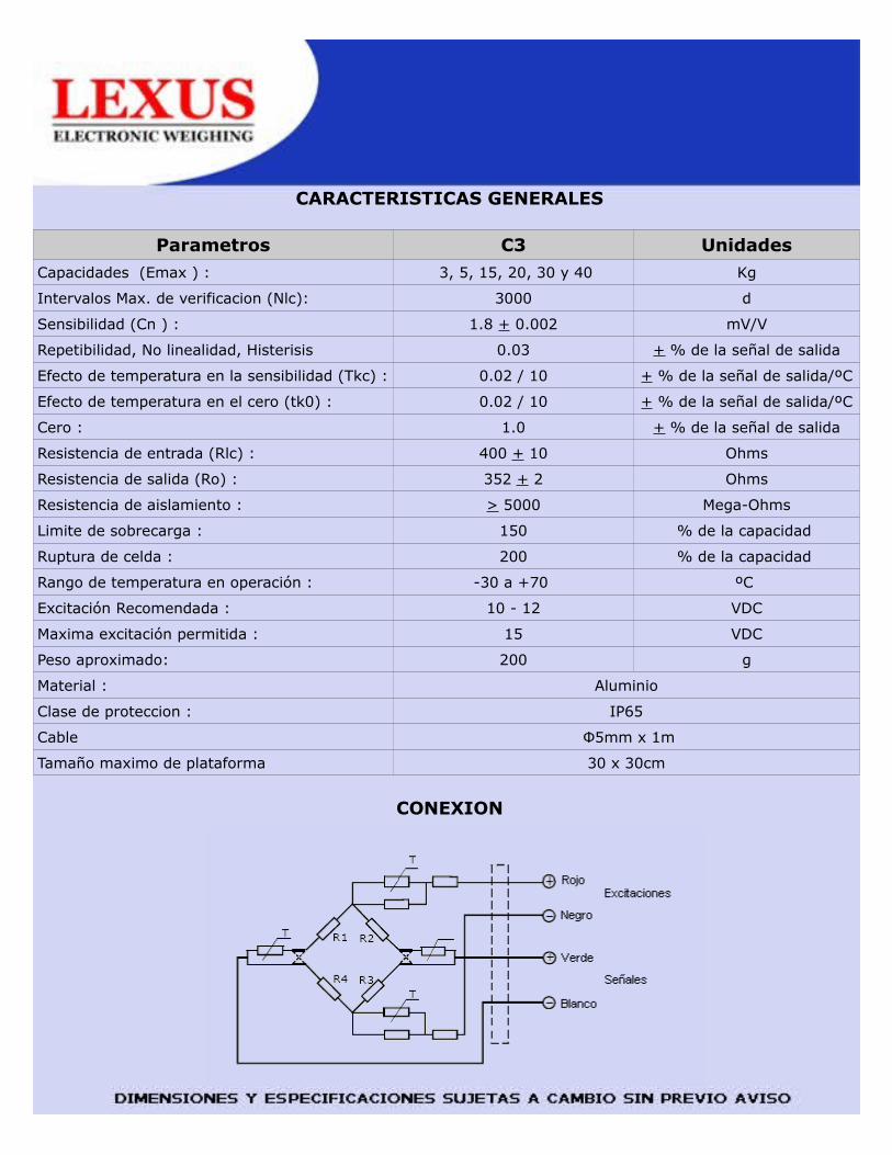
CARACTERISTICAS GENERALES
Parametros C3 UnidadesCapacidades (Emax ) : 3, 5, 15, 20, 30 y 40 Kg
Intervalos Max. de verificacion (Nlc): 3000 d
Sensibilidad (Cn ) : 1.8 + 0.002 mV/V
Repetibilidad, No linealidad, Histerisis 0.03 + % de la señal de salida
Efecto de temperatura en la sensibilidad (Tkc) : 0.02 / 10 + % de la señal de salida/ºC
Efecto de temperatura en el cero (tk0) : 0.02 / 10 + % de la señal de salida/ºC
Cero : 1.0 + % de la señal de salida
Resistencia de entrada (Rlc) : 400 + 10 Ohms
Resistencia de salida (Ro) : 352 + 2 Ohms
Resistencia de aislamiento : > 5000 Mega-Ohms
Limite de sobrecarga : 150 % de la capacidad
Ruptura de celda : 200 % de la capacidad
Rango de temperatura en operación : -30 a +70 ºC
Excitación Recomendada : 10 - 12 VDC
Maxima excitación permitida : 15 VDC
Peso aproximado: 200 g
Material : Aluminio
Clase de proteccion : IP65
Cable Φ5mm x 1m
Tamaño maximo de plataforma 30 x 30cm
CONEXION
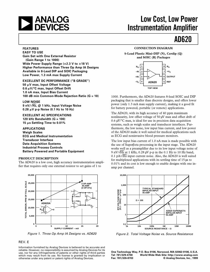
CONNECTION DIAGRAM
8-Lead Plastic Mini-DIP (N), Cerdip (Q)and SOIC (R) Packages
–IN
RG
–VS
+IN
RG
+VS
OUTPUT
REF
1
2
3
4
8
7
6
5AD620
TOP VIEW
REV. E
Information furnished by Analog Devices is believed to be accurate andreliable. However, no responsibility is assumed by Analog Devices for itsuse, nor for any infringements of patents or other rights of third partieswhich may result from its use. No license is granted by implication orotherwise under any patent or patent rights of Analog Devices.
a Low Cost, Low PowerInstrumentation Amplifier
AD620FEATURESEASY TO USEGain Set with One External Resistor
(Gain Range 1 to 1000)Wide Power Supply Range (62.3 V to 618 V)Higher Performance than Three Op Amp IA DesignsAvailable in 8-Lead DIP and SOIC PackagingLow Power, 1.3 mA max Supply Current
EXCELLENT DC PERFORMANCE (“B GRADE”)50 mV max, Input Offset Voltage0.6 mV/8C max, Input Offset Drift1.0 nA max, Input Bias Current100 dB min Common-Mode Rejection Ratio (G = 10)
LOW NOISE9 nV/√Hz, @ 1 kHz, Input Voltage Noise0.28 mV p-p Noise (0.1 Hz to 10 Hz)
EXCELLENT AC SPECIFICATIONS120 kHz Bandwidth (G = 100)15 ms Settling Time to 0.01%
APPLICATIONSWeigh ScalesECG and Medical InstrumentationTransducer InterfaceData Acquisition SystemsIndustrial Process ControlsBattery Powered and Portable Equipment
One Technology Way, P.O. Box 9106, Norwood, MA 02062-9106, U.S.A.Tel: 781/329-4700 World Wide Web Site: http://www.analog.comFax: 781/326-8703 © Analog Devices, Inc., 1999
PRODUCT DESCRIPTIONThe AD620 is a low cost, high accuracy instrumentation ampli-fier that requires only one external resistor to set gains of 1 to
0 5 10 15 20
30,000
5,000
10,000
15,000
20,000
25,000
0
TO
TA
L E
RR
OR
, PP
M O
F F
ULL
SC
ALE
SUPPLY CURRENT – mA
AD620A
RG
3 OP-AMP IN-AMP(3 OP-07s)
Figure 1. Three Op Amp IA Designs vs. AD620
SOURCE RESISTANCE – V100M10k1k 10M1M100k
10,000
0.1
100
1,000
10
1
RT
I VO
LTA
GE
NO
ISE
(0.1
– 1
0Hz)
– m
V p
-p
TYPICAL STANDARDBIPOLAR INPUTIN-AMP
AD620 SUPERbETABIPOLAR INPUTIN-AMP
G = 100
Figure 2. Total Voltage Noise vs. Source Resistance
1000. Furthermore, the AD620 features 8-lead SOIC and DIPpackaging that is smaller than discrete designs, and offers lowerpower (only 1.3 mA max supply current), making it a good fitfor battery powered, portable (or remote) applications.
The AD620, with its high accuracy of 40 ppm maximumnonlinearity, low offset voltage of 50 µV max and offset drift of0.6 µV/°C max, is ideal for use in precision data acquisitionsystems, such as weigh scales and transducer interfaces. Fur-thermore, the low noise, low input bias current, and low powerof the AD620 make it well suited for medical applications suchas ECG and noninvasive blood pressure monitors.
The low input bias current of 1.0 nA max is made possible withthe use of Superβeta processing in the input stage. The AD620works well as a preamplifier due to its low input voltage noise of9 nV/√Hz at 1 kHz, 0.28 µV p-p in the 0.1 Hz to 10 Hz band,0.1 pA/√Hz input current noise. Also, the AD620 is well suitedfor multiplexed applications with its settling time of 15 µs to0.01% and its cost is low enough to enable designs with one in-amp per channel.
AD620–SPECIFICATIONS (Typical @ +258C, VS = 615 V, and RL = 2 kV, unless otherwise noted)
AD620A AD620B AD620S1
Model Conditions Min Typ Max Min Typ Max Min Typ Max Units
GAIN G = 1 + (49.4 k/RG)Gain Range 1 10,000 1 10,000 1 10,000Gain Error2 VOUT = ± 10 V
G = 1 0.03 0.10 0.01 0.02 0.03 0.10 %G = 10 0.15 0.30 0.10 0.15 0.15 0.30 %G = 100 0.15 0.30 0.10 0.15 0.15 0.30 %G = 1000 0.40 0.70 0.35 0.50 0.40 0.70 %
Nonlinearity, VOUT = –10 V to +10 V,G = 1–1000 RL = 10 kΩ 10 40 10 40 10 40 ppmG = 1–100 RL = 2 kΩ 10 95 10 95 10 95 ppm
Gain vs. TemperatureG =1 10 10 10 ppm/°CGain >12 –50 –50 –50 ppm/°C
VOLTAGE OFFSET (Total RTI Error = VOSI + VOSO/G)Input Offset, VOSI VS = ±5 V to ±15 V 30 125 15 50 30 125 µV
Over Temperature VS = ±5 V to ±15 V 185 85 225 µVAverage TC VS = ±5 V to ±15 V 0.3 1.0 0.1 0.6 0.3 1.0 µV/°C
Output Offset, VOSO VS = ±15 V 400 1000 200 500 400 1000 µVVS = ±5 V 1500 750 1500 µV
Over Temperature VS = ±5 V to ±15 V 2000 1000 2000 µVAverage TC VS = ± 5 V to ±15 V 5.0 15 2.5 7.0 5.0 15 µV/°C
Offset Referred to theInput vs.Supply (PSR) VS = ±2.3 V to ±18 V
G = 1 80 100 80 100 80 100 dBG = 10 95 120 100 120 95 120 dBG = 100 110 140 120 140 110 140 dBG = 1000 110 140 120 140 110 140 dB
INPUT CURRENTInput Bias Current 0.5 2.0 0.5 1.0 0.5 2 nA
Over Temperature 2.5 1.5 4 nAAverage TC 3.0 3.0 8.0 pA/°C
Input Offset Current 0.3 1.0 0.3 0.5 0.3 1.0 nAOver Temperature 1.5 0.75 2.0 nAAverage TC 1.5 1.5 8.0 pA/°C
INPUTInput Impedance
Differential 10i2 10i2 10i2 GΩipFCommon-Mode 10i2 10i2 10i2 GΩipF
Input Voltage Range3 VS = ±2.3 V to ±5 V –VS + 1.9 +VS – 1.2 –VS + 1.9 +VS – 1.2 –VS + 1.9 +VS – 1.2 VOver Temperature –VS + 2.1 +VS – 1.3 –VS + 2.1 +VS – 1.3 –VS + 2.1 +VS – 1.3 V
VS = ±5 V to ±18 V –VS + 1.9 +VS – 1.4 –VS + 1.9 +VS – 1.4 –VS + 1.9 +VS – 1.4 VOver Temperature –VS + 2.1 +VS – 1.4 –VS + 2.1 +VS – 1.4 –VS + 2.3 +VS – 1.4 V
Common-Mode RejectionRatio DC to 60 Hz withI kΩ Source Imbalance VCM = 0 V to ±10 V
G = 1 73 90 80 90 73 90 dBG = 10 93 110 100 110 93 110 dBG = 100 110 130 120 130 110 130 dBG = 1000 110 130 120 130 110 130 dB
OUTPUTOutput Swing RL = 10 kΩ,
VS = ±2.3 V to ±5 V –VS + 1.1 +VS – 1.2 –VS + 1.1 +VS – 1.2 –VS + 1.1 +VS – 1.2 VOver Temperature –VS + 1.4 +VS – 1.3 –VS + 1.4 +VS – 1.3 –VS + 1.6 +VS – 1.3 V
VS = ±5 V to ±18 V –VS + 1.2 +VS – 1.4 –VS + 1.2 +VS – 1.4 –VS + 1.2 +VS – 1.4 VOver Temperature –VS + 1.6 +VS – 1.5 –VS + 1.6 +VS – 1.5 –VS + 2.3 +VS – 1.5 V
Short Current Circuit ± 18 ± 18 ± 18 mA
REV. E–2–
AD620AD620A AD620B AD620S1
Model Conditions Min Typ Max Min Typ Max Min Typ Max Units
DYNAMIC RESPONSESmall Signal –3 dB Bandwidth
G = 1 1000 1000 1000 kHzG = 10 800 800 800 kHzG = 100 120 120 120 kHzG = 1000 12 12 12 kHz
Slew Rate 0.75 1.2 0.75 1.2 0.75 1.2 V/µsSettling Time to 0.01% 10 V Step
G = 1–100 15 15 15 µsG = 1000 150 150 150 µs
NOISE
Voltage Noise, 1 kHz Total RTI Noise = (e2
ni )+(eno /G)2
Input, Voltage Noise, eni 9 13 9 13 9 13 nV/√HzOutput, Voltage Noise, eno 72 100 72 100 72 100 nV/√Hz
RTI, 0.1 Hz to 10 HzG = 1 3.0 3.0 6.0 3.0 6.0 µV p-pG = 10 0.55 0.55 0.8 0.55 0.8 µV p-pG = 100–1000 0.28 0.28 0.4 0.28 0.4 µV p-p
Current Noise f = 1 kHz 100 100 100 fA/√Hz0.1 Hz to 10 Hz 10 10 10 pA p-p
REFERENCE INPUTRIN 20 20 20 kΩIIN VIN+, VREF = 0 +50 +60 +50 +60 +50 +60 µAVoltage Range –VS + 1.6 +VS – 1.6 –VS + 1.6 +VS – 1.6 –VS + 1.6 +VS – 1.6 VGain to Output 1 ± 0.0001 1 ± 0.0001 1 ± 0.0001
POWER SUPPLYOperating Range4 ± 2.3 ± 18 ± 2.3 ± 18 ± 2.3 ± 18 VQuiescent Current VS = ±2.3 V to ±18 V 0.9 1.3 0.9 1.3 0.9 1.3 mA
Over Temperature 1.1 1.6 1.1 1.6 1.1 1.6 mA
TEMPERATURE RANGEFor Specified Performance –40 to +85 –40 to +85 –55 to +125 °C
NOTES1See Analog Devices military data sheet for 883B tested specifications.2Does not include effects of external resistor RG.3One input grounded. G = 1.4This is defined as the same supply range which is used to specify PSR.
Specifications subject to change without notice.
REV. E –3–
AD620
REV. E–4–
NOTES1Stresses above those listed under Absolute Maximum Ratings may cause perma-
nent damage to the device. This is a stress rating only; functional operation of thedevice at these or any other conditions above those indicated in the operationalsection of this specification is not implied. Exposure to absolute maximum ratingconditions for extended periods may affect device reliability.
2Specification is for device in free air:8-Lead Plastic Package: θJA = 95°C/W8-Lead Cerdip Package: θJA = 110°C/W8-Lead SOIC Package: θJA = 155°C/W
ABSOLUTE MAXIMUM RATINGS1
Supply Voltage . . . . . . . . . . . . . . . . . . . . . . . . . . . . . . . . . ±18 VInternal Power Dissipation2 . . . . . . . . . . . . . . . . . . . . . 650 mWInput Voltage (Common Mode) . . . . . . . . . . . . . . . . . . . . ±VS
Differential Input Voltage . . . . . . . . . . . . . . . . . . . . . . . .±25 VOutput Short Circuit Duration . . . . . . . . . . . . . . . . . IndefiniteStorage Temperature Range (Q) . . . . . . . . . . –65°C to +150°CStorage Temperature Range (N, R) . . . . . . . . –65°C to +125°COperating Temperature Range
AD620 (A, B) . . . . . . . . . . . . . . . . . . . . . . –40°C to +85°CAD620 (S) . . . . . . . . . . . . . . . . . . . . . . . . –55°C to +125°C
Lead Temperature Range(Soldering 10 seconds) . . . . . . . . . . . . . . . . . . . . . . . +300°C
ORDERING GUIDE
Model Temperature Ranges Package Options*
AD620AN –40°C to +85°C N-8AD620BN –40°C to +85°C N-8AD620AR –40°C to +85°C SO-8AD620AR-REEL –40°C to +85°C 13" REELAD620AR-REEL7 –40°C to +85°C 7" REELAD620BR –40°C to +85°C SO-8AD620BR-REEL –40°C to +85°C 13" REELAD620BR-REEL7 –40°C to +85°C 7" REELAD620ACHIPS –40°C to +85°C Die FormAD620SQ/883B –55°C to +125°C Q-8
*N = Plastic DIP; Q = Cerdip; SO = Small Outline.
METALIZATION PHOTOGRAPHDimensions shown in inches and (mm).Contact factory for latest dimensions.
+VS OUTPUT
REFERENCE
+IN–VS
–IN
*FOR CHIP APPLICATIONS: THE PADS 1R G AND 8RG MUST BE CONNECTED IN PARALLEL TO THE EXTERNAL GAIN REGISTER R G. DO NOT CONNECT THEM IN SERIES TO RG. FOR UNITY GAIN APPLICATIONS WHERE R G IS NOT REQUIRED, THE PADS 1RG MAY SIMPLY BE BONDED TOGETHER, AS WELL AS THE PADS 8R G.
4
5
678
8
RG*
1
1 2 3
RG*0.125
(3.180)
0.0708(1.799)
CAUTIONESD (electrostatic discharge) sensitive device. Electrostatic charges as high as 4000 V readilyaccumulate on the human body and test equipment and can discharge without detection.Although the AD620 features proprietary ESD protection circuitry, permanent damage mayoccur on devices subjected to high energy electrostatic discharges. Therefore, proper ESDprecautions are recommended to avoid performance degradation or loss of functionality.
WARNING!
ESD SENSITIVE DEVICE
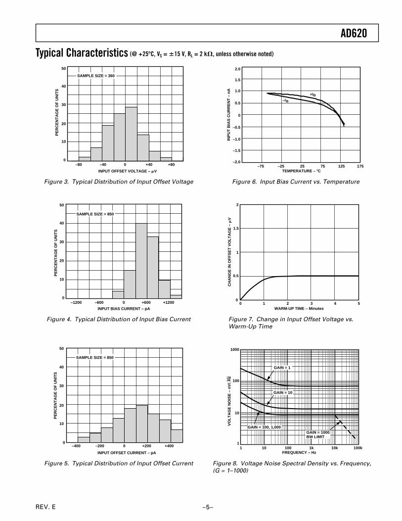
AD620
REV. E –5–
Typical Characteristics (@ +258C, VS = 615 V, RL = 2 kV, unless otherwise noted)
INPUT OFFSET VOLTAGE – mV
20
30
40
50
–40 0 +40 +80
PE
RC
EN
TA
GE
OF
UN
ITS
–80
SAMPLE SIZE = 360
10
0
Figure 3. Typical Distribution of Input Offset Voltage
INPUT BIAS CURRENT – pA
0
10
20
30
40
50
–600 0 +600
PE
RC
EN
TA
GE
OF
UN
ITS
–1200 +1200
SAMPLE SIZE = 850
Figure 4. Typical Distribution of Input Bias Current
10
20
30
40
50
–200 0 +200 +400
INPUT OFFSET CURRENT – pA
PE
RC
EN
TA
GE
OF
UN
ITS
–4000
SAMPLE SIZE = 850
Figure 5. Typical Distribution of Input Offset Current
TEMPERATURE – 8C
INP
UT
BIA
S C
UR
RE
NT
– n
A
+IB–IB
2.0
–2.0175
–1.0
–1.5
–75
–0.5
0
0.5
1.0
1.5
1257525–25
Figure 6. Input Bias Current vs. Temperature
CH
AN
GE
IN O
FF
SE
T V
OLT
AG
E –
mV
1.5
0.5
WARM-UP TIME – Minutes
2
00 51
1
432
Figure 7. Change in Input Offset Voltage vs.Warm-Up Time
FREQUENCY – Hz
1000
11 100k
100
10
10k1k100
VO
LTA
GE
NO
ISE
– n
V/!
Hz
GAIN = 1
GAIN = 10
10
GAIN = 100, 1,000GAIN = 1000BW LIMIT
Figure 8. Voltage Noise Spectral Density vs. Frequency,(G = 1–1000)
AD620–Typical Characteristics
FREQUENCY – Hz
1000
100
101 10 1000100
CU
RR
EN
T N
OIS
E –
fA/!
Hz
Figure 9. Current Noise Spectral Density vs. Frequency
RT
I NO
ISE
– 2
.0 m
V/D
IV
TIME – 1 SEC/DIV
Figure 10a. 0.1 Hz to 10 Hz RTI Voltage Noise (G = 1)
RT
I NO
ISE
– 0
.1m
V/D
IV
TIME – 1 SEC/DIV
Figure 10b. 0.1 Hz to 10 Hz RTI Voltage Noise (G = 1000)
Figure 11. 0.1 Hz to 10 Hz Current Noise, 5 pA/Div
100
1000
AD620A
FET INPUTIN-AMP
SOURCE RESISTANCE – V
TO
TA
L D
RIF
T F
RO
M 2
58C
TO
858
C, R
TI –
mV
100,000
101k 10M
10,000
10k 1M100k
Figure 12. Total Drift vs. Source Resistance
FREQUENCY – Hz
CM
R –
dB
+160
01M
+80
+40
1
+60
0.1
+140
+100
+120
100k10k1k10010
G = 1000
G = 100
G = 10
G = 1
+20
Figure 13. CMR vs. Frequency, RTI, Zero to 1 kΩ SourceImbalance
REV. E–6–
AD620
REV. E –7–
FREQUENCY – Hz
PS
R –
dB
160
1M
80
40
1
60
0.1
140
100
120
100k10k1k1001020
G = 1000
G = 100
G = 10
G = 1
180
Figure 14. Positive PSR vs. Frequency, RTI (G = 1–1000)
FREQUENCY – Hz
PS
R –
dB
160
1M
80
40
1
60
0.1
140
100
120
100k10k1k1001020
180
G = 10
G = 100
G = 1
G = 1000
Figure 15. Negative PSR vs. Frequency, RTI (G = 1–1000)
1000
100 10M
100
1
1k
10
100k 1M10k FREQUENCY – Hz
GA
IN –
V/V
0.1
Figure 16. Gain vs. Frequency
OU
TP
UT
VO
LTA
GE
– V
olts
p-p
FREQUENCY – Hz
35
01M
15
5
10k
10
1k
30
20
25
100k
G = 10, 100, 1000
G = 1
G = 1000 G = 100
BW
LIM
IT
Figure 17. Large Signal Frequency Response
INP
UT
VO
LTA
GE
LIM
IT –
Vol
ts(R
EF
ER
RE
D T
O S
UP
PLY
VO
LTA
GE
S)
20
+1.0
+0.5
50
+1.5
–1.5
–1.0
–0.5
1510SUPPLY VOLTAGE 6 Volts
+VS –0.0
–VS +0.0
Figure 18. Input Voltage Range vs. Supply Voltage, G = 1
20
+1.0
+0.5
50
+1.5
–1.5
–1.0
–0.5
1510SUPPLY VOLTAGE 6 Volts
RL = 10kV
RL = 2kV
RL = 10kV
OU
TP
UT
VO
LTA
GE
SW
ING
– V
olts
(RE
FE
RR
ED
TO
SU
PP
LY V
OLT
AG
ES
)
RL = 2kV
+VS –0.0
–VS +0.0
Figure 19. Output Voltage Swing vs. Supply Voltage,G = 10
AD620
REV. E–8–
OU
TP
UT
VO
LTA
GE
SW
ING
– V
olts
p-p
LOAD RESISTANCE – V
30
00 10k
20
10
100 1k
VS = 615VG = 10
Figure 20. Output Voltage Swing vs. Load Resistance
. . . . . . . . . . . . . . . . . . . . . . . . . . . . . . . . . . . . . . . .
. . . . . . . . . . . . . . . . . . . . . . . . . . . . . . . . . . . . . . . .
Figure 21. Large Signal Pulse Response and Settling TimeG = 1 (0.5 mV = 0.01%)
. . . . . . . . . . . . . . . . . . . . . . . . . . . . . . . . . . . . . . . .
. . . . . . . . . . . . . . . . . . . . . . . . . . . . . . . . . . . . . . . .
Figure 22. Small Signal Response, G = 1, RL = 2 kΩ,CL = 100 pF
. . . . . . . . . . . . . . . . . . . . . . . . . . . . . . . . . . . . . . . .
. . . . . . . . . . . . . . . . . . . . . . . . . . . . . . . . . . . . . . . .
Figure 23. Large Signal Response and Settling Time,G = 10 (0.5 mV = 001%)
. . . . . . . . . . . . . . . . . . . . . . . . . . . . . . . . . . . . . . . .
. . . . . . . . . . . . . . . . . . . . . . . . . . . . . . . . . . . . . . . .
Figure 24. Small Signal Response, G = 10, RL = 2 kΩ,CL = 100 pF
. . . . . . . . . . . . . . . . . . . . . . . . . . . . . . . . . . . . . . . .
. . . . . . . . . . . . . . . . . . . . . . . . . . . . . . . . . . . . . . . .
Figure 25. Large Signal Response and Settling Time,G = 100 (0.5 mV = 0.01%)
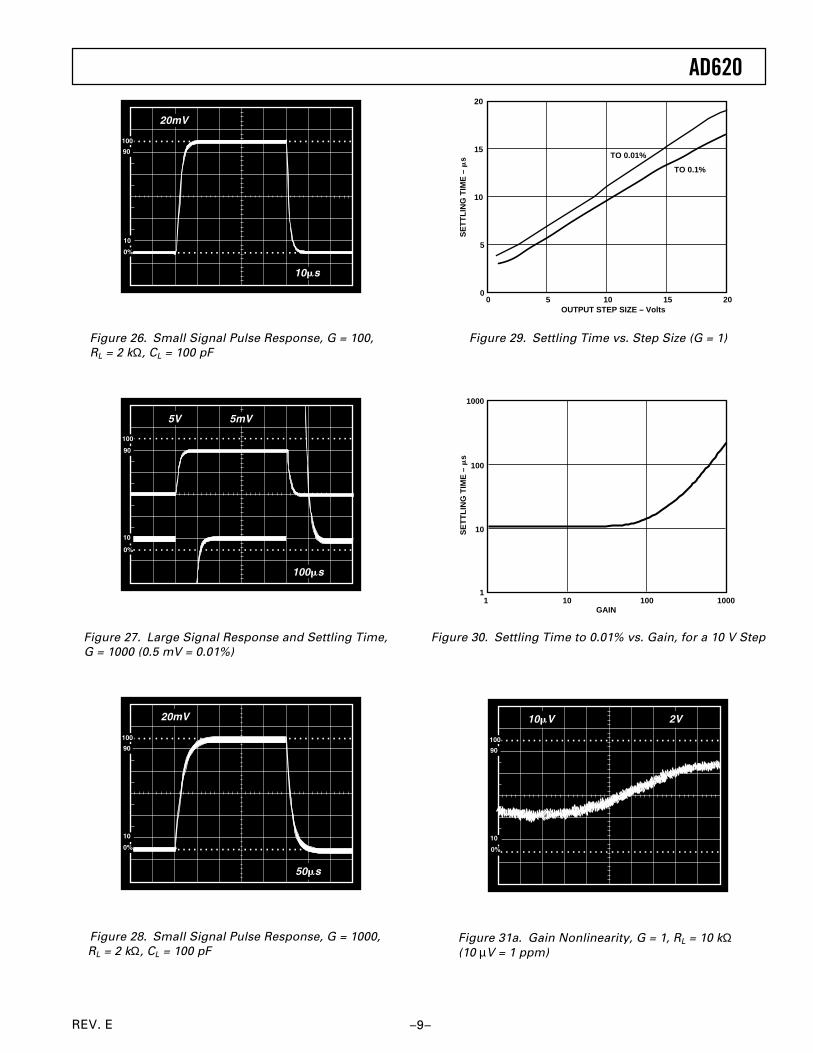
AD620
REV. E –9–
. . . . . . . . . . . . . . . . . . . . . . . . . . . . . . . . . . . . . . . .
. . . . . . . . . . . . . . . . . . . . . . . . . . . . . . . . . . . . . . . .
Figure 26. Small Signal Pulse Response, G = 100,RL = 2 kΩ, CL = 100 pF
. . . . . . . . . . . . . . . . . . . . . . . . . . . . . . . . . . . . . . . .
. . . . . . . . . . . . . . . . . . . . . . . . . . . . . . . . . . . . . . . .
Figure 27. Large Signal Response and Settling Time,G = 1000 (0.5 mV = 0.01%)
. . . . . . . . . . . . . . . . . . . . . . . . . . . . . . . . . . . . . . . .
. . . . . . . . . . . . . . . . . . . . . . . . . . . . . . . . . . . . . . . .
Figure 28. Small Signal Pulse Response, G = 1000,RL = 2 kΩ, CL = 100 pF
OUTPUT STEP SIZE – Volts
SE
TT
LIN
G T
IME
– m
s TO 0.01%
TO 0.1%
20
00 20
15
5
5
10
10 15
Figure 29. Settling Time vs. Step Size (G = 1)
GAIN
SE
TT
LIN
G T
IME
– m
s
1000
11 1000
100
10
10 100
Figure 30. Settling Time to 0.01% vs. Gain, for a 10 V Step
. . . . . . . . . . . . . . . . . . . . . . . . . . . . . . . . . . . . . . . .
. . . . . . . . . . . . . . . . . . . . . . . . . . . . . . . . . . . . . . . .
Figure 31a. Gain Nonlinearity, G = 1, RL = 10 kΩ(10 µV = 1 ppm)
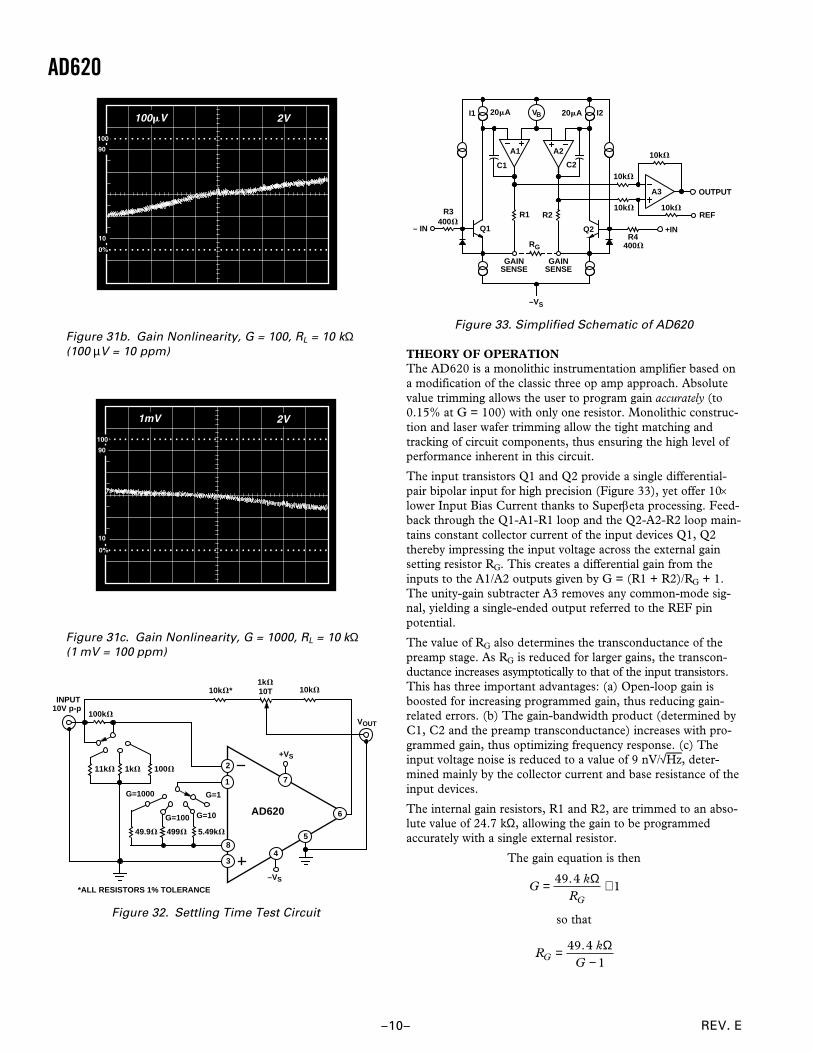
AD620
REV. E–10–
VB
–VS
A1 A2
A3
C2
RG
R1 R2
GAINSENSE
GAINSENSE
R3400V
10kV
10kV
I2I1
10kVREF
10kV
+IN– IN
20mA 20mA
R4400V
OUTPUT
C1
Q2Q1
Figure 33. Simplified Schematic of AD620
THEORY OF OPERATIONThe AD620 is a monolithic instrumentation amplifier based ona modification of the classic three op amp approach. Absolutevalue trimming allows the user to program gain accurately (to0.15% at G = 100) with only one resistor. Monolithic construc-tion and laser wafer trimming allow the tight matching andtracking of circuit components, thus ensuring the high level ofperformance inherent in this circuit.
The input transistors Q1 and Q2 provide a single differential-pair bipolar input for high precision (Figure 33), yet offer 10×lower Input Bias Current thanks to Superβeta processing. Feed-back through the Q1-A1-R1 loop and the Q2-A2-R2 loop main-tains constant collector current of the input devices Q1, Q2thereby impressing the input voltage across the external gainsetting resistor RG. This creates a differential gain from theinputs to the A1/A2 outputs given by G = (R1 + R2)/RG + 1.The unity-gain subtracter A3 removes any common-mode sig-nal, yielding a single-ended output referred to the REF pinpotential.
The value of RG also determines the transconductance of thepreamp stage. As RG is reduced for larger gains, the transcon-ductance increases asymptotically to that of the input transistors.This has three important advantages: (a) Open-loop gain isboosted for increasing programmed gain, thus reducing gain-related errors. (b) The gain-bandwidth product (determined byC1, C2 and the preamp transconductance) increases with pro-grammed gain, thus optimizing frequency response. (c) Theinput voltage noise is reduced to a value of 9 nV/√Hz, deter-mined mainly by the collector current and base resistance of theinput devices.
The internal gain resistors, R1 and R2, are trimmed to an abso-lute value of 24.7 kΩ, allowing the gain to be programmedaccurately with a single external resistor.
The gain equation is then
G = 49.4 kΩ
RG+ 1
so that
RG = 49.4 kΩ
G − 1
. . . . . . . . . . . . . . . . . . . . . . . . . . . . . . . . . . . . . . . .
. . . . . . . . . . . . . . . . . . . . . . . . . . . . . . . . . . . . . . . .
Figure 31b. Gain Nonlinearity, G = 100, RL = 10 kΩ(100 µV = 10 ppm)
. . . . . . . . . . . . . . . . . . . . . . . . . . . . . . . . . . . . . . . .
. . . . . . . . . . . . . . . . . . . . . . . . . . . . . . . . . . . . . . . .
Figure 31c. Gain Nonlinearity, G = 1000, RL = 10 kΩ(1 mV = 100 ppm)
AD620
VOUT
G=1G=1000
49.9V
10kV*1kV10T 10kV
499V
G=10G=100
5.49kV
+VS
11kV 1kV 100V
100kV
INPUT10V p-p
–VS
*ALL RESISTORS 1% TOLERANCE
71
2
3
8
6
4
5
Figure 32. Settling Time Test Circuit
AD620
REV. E –11–
Make vs. Buy: A Typical Bridge Application Error BudgetThe AD620 offers improved performance over “homebrew”three op amp IA designs, along with smaller size, fewer compo-nents and 10× lower supply current. In the typical application,shown in Figure 34, a gain of 100 is required to amplify a bridgeoutput of 20 mV full scale over the industrial temperature rangeof –40°C to +85°C. The error budget table below shows how tocalculate the effect various error sources have on circuit accuracy.
Regardless of the system in which it is being used, the AD620provides greater accuracy, and at low power and price. In simple
R = 350V
+10V
PRECISION BRIDGE TRANSDUCERAD620A MONOLITHICINSTRUMENTATIONAMPLIFIER, G = 100
“HOMEBREW” IN-AMP, G = 100 *0.02% RESISTOR MATCH, 3PPM/8C TRACKING**DISCRETE 1% RESISTOR, 100PPM/8C TRACKING SUPPLY CURRENT = 15mA MAX
100V**
10kV*
10kV**
10kV*
10kV*
10kV**
10kV*
SUPPLY CURRENT = 1.3mA MAX
OP07D
OP07D
OP07DAD620ARG
499V
REFERENCE
R = 350V R = 350V
R = 350V
Figure 34. Make vs. Buy
Table I. Make vs. Buy Error Budget
AD620 Circuit “Homebrew” Circuit Error, ppm of Full ScaleError Source Calculation Calculation AD620 Homebrew
ABSOLUTE ACCURACY at TA = +25°CInput Offset Voltage, µV 125 µV/20 mV (150 µV × √2)/20 mV 16,250 10,607Output Offset Voltage, µV 1000 µV/100/20 mV ((150 µV × 2)/100)/20 mV 14,500 10,150Input Offset Current, nA 2 nA × 350 Ω/20 mV (6 nA × 350 Ω)/20 mV 14,118 14,153CMR, dB 110 dB→3.16 ppm, × 5 V/20 mV (0.02% Match × 5 V)/20 mV/100 14,791 10,500
Total Absolute Error 17,558 11,310DRIFT TO +85°C
Gain Drift, ppm/°C (50 ppm + 10 ppm) × 60°C 100 ppm/°C Track × 60°C 13,600 16,000Input Offset Voltage Drift, µV/°C 1 µV/°C × 60°C/20 mV (2.5 µV/°C × √2 × 60°C)/20 mV 13,000 10,607Output Offset Voltage Drift, µV/°C 15 µV/°C × 60°C/100/20 mV (2.5 µV/°C × 2 × 60°C)/100/20 mV 14,450 10,150
Total Drift Error 17,050 16,757RESOLUTION
Gain Nonlinearity, ppm of Full Scale 40 ppm 40 ppm 14,140 10,140Typ 0.1 Hz–10 Hz Voltage Noise, µV p-p 0.28 µV p-p/20 mV (0.38 µV p-p × √2)/20 mV 141,14 13,127
Total Resolution Error 14,154 101,67
Grand Total Error 14,662 28,134
G = 100, VS = ± 15 V.
(All errors are min/max and referred to input.)
systems, absolute accuracy and drift errors are by far the mostsignificant contributors to error. In more complex systems withan intelligent processor, an autogain/autozero cycle will remove allabsolute accuracy and drift errors leaving only the resolutionerrors of gain nonlinearity and noise, thus allowing full 14-bitaccuracy.
Note that for the homebrew circuit, the OP07 specifications forinput voltage offset and noise have been multiplied by √2. Thisis because a three op amp type in-amp has two op amps at itsinputs, both contributing to the overall input error.
AD620
REV. E–12–
3kV
+5V
DIGITALDATAOUTPUT
ADC
REF
IN
AGND
20kV
10kV
20kV
AD620BG=100
1.7mA 0.10mA0.6mAMAX
499V
3kV
3kV3kV
2
1
8
37
6
5
4
1.3mAMAX
AD705
Figure 35. A Pressure Monitor Circuit which Operates on a +5 V Single Supply
Pressure MeasurementAlthough useful in many bridge applications such as weighscales, the AD620 is especially suitable for higher resistancepressure sensors powered at lower voltages where small size andlow power become more significant.
Figure 35 shows a 3 kΩ pressure transducer bridge poweredfrom +5 V. In such a circuit, the bridge consumes only 1.7 mA.Adding the AD620 and a buffered voltage divider allows thesignal to be conditioned for only 3.8 mA of total supply current.
Small size and low cost make the AD620 especially attractive forvoltage output pressure transducers. Since it delivers low noiseand drift, it will also serve applications such as diagnostic non-invasive blood pressure measurement.
Medical ECGThe low current noise of the AD620 allows its use in ECGmonitors (Figure 36) where high source resistances of 1 MΩ orhigher are not uncommon. The AD620’s low power, low supplyvoltage requirements, and space-saving 8-lead mini-DIP andSOIC package offerings make it an excellent choice for batterypowered data recorders.
Furthermore, the low bias currents and low current noisecoupled with the low voltage noise of the AD620 improve thedynamic range for better performance.
The value of capacitor C1 is chosen to maintain stability of theright leg drive loop. Proper safeguards, such as isolation, mustbe added to this circuit to protect the patient from possibleharm.
G = 7
AD620A0.03HzHIGHPASS
FILTER
OUTPUT1V/mV
+3V
–3V
RG8.25kV
24.9kV
24.9kV
AD705J
G = 143C1
1MVR4
10kVR1 R3
R2
OUTPUTAMPLIFIER
PATIENT/CIRCUITPROTECTION/ISOLATION
Figure 36. A Medical ECG Monitor Circuit
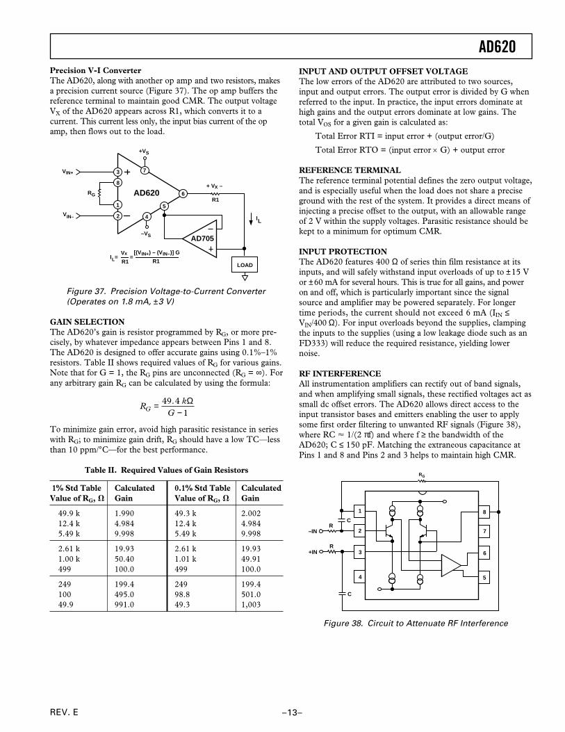
AD620
REV. E –13–
Precision V-I ConverterThe AD620, along with another op amp and two resistors, makesa precision current source (Figure 37). The op amp buffers thereference terminal to maintain good CMR. The output voltageVX of the AD620 appears across R1, which converts it to acurrent. This current less only, the input bias current of the opamp, then flows out to the load.
AD620RG
–VS
VIN+
VIN–
LOAD
R1
IL
VxI =L R1
=IN+[(V ) – (V )] GIN–
R1
6
5
+ V –X
42
1
8
3 7
+VS
AD705
Figure 37. Precision Voltage-to-Current Converter(Operates on 1.8 mA, ±3 V)
GAIN SELECTIONThe AD620’s gain is resistor programmed by RG, or more pre-cisely, by whatever impedance appears between Pins 1 and 8.The AD620 is designed to offer accurate gains using 0.1%–1%resistors. Table II shows required values of RG for various gains.Note that for G = 1, the RG pins are unconnected (RG = ∞). Forany arbitrary gain RG can be calculated by using the formula:
RG = 49.4 kΩ
G − 1
To minimize gain error, avoid high parasitic resistance in serieswith RG; to minimize gain drift, RG should have a low TC—lessthan 10 ppm/°C—for the best performance.
Table II. Required Values of Gain Resistors
1% Std Table Calculated 0.1% Std Table CalculatedValue of RG, V Gain Value of RG, V Gain
49.9 k 1.990 49.3 k 2.00212.4 k 4.984 12.4 k 4.9845.49 k 9.998 5.49 k 9.998
2.61 k 19.93 2.61 k 19.931.00 k 50.40 1.01 k 49.91499 100.0 499 100.0
249 199.4 249 199.4100 495.0 98.8 501.049.9 991.0 49.3 1,003
INPUT AND OUTPUT OFFSET VOLTAGEThe low errors of the AD620 are attributed to two sources,input and output errors. The output error is divided by G whenreferred to the input. In practice, the input errors dominate athigh gains and the output errors dominate at low gains. Thetotal VOS for a given gain is calculated as:
Total Error RTI = input error + (output error/G)
Total Error RTO = (input error × G) + output error
REFERENCE TERMINALThe reference terminal potential defines the zero output voltage,and is especially useful when the load does not share a preciseground with the rest of the system. It provides a direct means ofinjecting a precise offset to the output, with an allowable rangeof 2 V within the supply voltages. Parasitic resistance should bekept to a minimum for optimum CMR.
INPUT PROTECTIONThe AD620 features 400 Ω of series thin film resistance at itsinputs, and will safely withstand input overloads of up to ±15 Vor ±60 mA for several hours. This is true for all gains, and poweron and off, which is particularly important since the signalsource and amplifier may be powered separately. For longertime periods, the current should not exceed 6 mA (IIN ≤VIN/400 Ω). For input overloads beyond the supplies, clampingthe inputs to the supplies (using a low leakage diode such as anFD333) will reduce the required resistance, yielding lowernoise.
RF INTERFERENCEAll instrumentation amplifiers can rectify out of band signals,and when amplifying small signals, these rectified voltages act assmall dc offset errors. The AD620 allows direct access to theinput transistor bases and emitters enabling the user to applysome first order filtering to unwanted RF signals (Figure 38),where RC < 1/(2 πf) and where f ≥ the bandwidth of theAD620; C ≤ 150 pF. Matching the extraneous capacitance atPins 1 and 8 and Pins 2 and 3 helps to maintain high CMR.
–IN
1
2
3
4 5
6
7
8
R
R+IN
C
C
RG
Figure 38. Circuit to Attenuate RF Interference
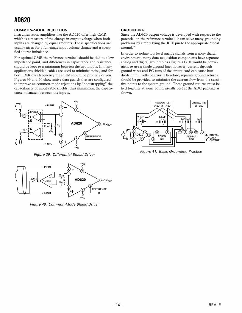
AD620
REV. E–14–
COMMON-MODE REJECTIONInstrumentation amplifiers like the AD620 offer high CMR,which is a measure of the change in output voltage when bothinputs are changed by equal amounts. These specifications areusually given for a full-range input voltage change and a speci-fied source imbalance.
For optimal CMR the reference terminal should be tied to a lowimpedance point, and differences in capacitance and resistanceshould be kept to a minimum between the two inputs. In manyapplications shielded cables are used to minimize noise, and forbest CMR over frequency the shield should be properly driven.Figures 39 and 40 show active data guards that are configuredto improve ac common-mode rejections by “bootstrapping” thecapacitances of input cable shields, thus minimizing the capaci-tance mismatch between the inputs.
REFERENCE
VOUTAD620
100V
100V
– INPUT
+ INPUT
AD648
RG
–VS
+VS
–VS
Figure 39. Differential Shield Driver
100V
– INPUT
+ INPUT
REFERENCE
VOUTAD620
–VS
+VS
2RG
2RG
AD548
Figure 40. Common-Mode Shield Driver
GROUNDINGSince the AD620 output voltage is developed with respect to thepotential on the reference terminal, it can solve many groundingproblems by simply tying the REF pin to the appropriate “localground.”
In order to isolate low level analog signals from a noisy digitalenvironment, many data-acquisition components have separateanalog and digital ground pins (Figure 41). It would be conve-nient to use a single ground line; however, current throughground wires and PC runs of the circuit card can cause hun-dreds of millivolts of error. Therefore, separate ground returnsshould be provided to minimize the current flow from the sensi-tive points to the system ground. These ground returns must betied together at some point, usually best at the ADC package asshown.
DIGITAL P.S.+5VC
ANALOG P.S.+15V C –15V
AD574ADIGITALDATAOUTPUT
+
1mF
AD620
0.1mF
AD585S/H ADC
0.1mF1mF 1mF
Figure 41. Basic Grounding Practice
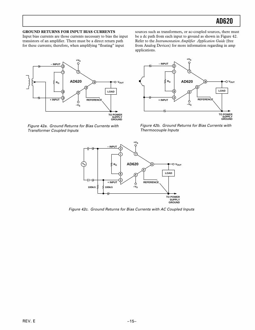
AD620
REV. E –15–
GROUND RETURNS FOR INPUT BIAS CURRENTSInput bias currents are those currents necessary to bias the inputtransistors of an amplifier. There must be a direct return pathfor these currents; therefore, when amplifying “floating” input
VOUTAD620
– INPUT
RG
TO POWERSUPPLY
GROUND
REFERENCE+ INPUT
+VS
–VS
LOAD
Figure 42a. Ground Returns for Bias Currents withTransformer Coupled Inputs
sources such as transformers, or ac-coupled sources, there mustbe a dc path from each input to ground as shown in Figure 42.Refer to the Instrumentation Amplifier Application Guide (freefrom Analog Devices) for more information regarding in ampapplications.
VOUT
– INPUT
+ INPUT
RG
LOAD
TO POWERSUPPLY
GROUND
REFERENCE
+VS
–VS
AD620
Figure 42b. Ground Returns for Bias Currents withThermocouple Inputs
100kV
VOUTAD620
– INPUT
+ INPUT
RG
LOAD
TO POWERSUPPLY
GROUND
REFERENCE
100kV –VS
+VS
Figure 42c. Ground Returns for Bias Currents with AC Coupled Inputs
AD620
REV. E–16–
OUTLINE DIMENSIONSDimensions shown in inches and (mm).
Plastic DIP (N-8) Package
8
1 4
5
0.430 (10.92)0.348 (8.84)
0.280 (7.11)0.240 (6.10)
PIN 1
SEATINGPLANE
0.022 (0.558)0.014 (0.356)
0.060 (1.52)0.015 (0.38)
0.210 (5.33)MAX 0.130
(3.30)MIN
0.070 (1.77)0.045 (1.15)
0.100(2.54)BSC
0.160 (4.06)0.115 (2.93)
0.325 (8.25)0.300 (7.62)
0.015 (0.381)0.008 (0.204)
0.195 (4.95)0.115 (2.93)
Cerdip (Q-8) Package
8
1 4
5
0.310 (7.87)0.220 (5.59)
PIN 1
0.005 (0.13)MIN
0.055 (1.4)MAX
SEATINGPLANE
0.023 (0.58)0.014 (0.36)
0.200 (5.08)MAX 0.150
(3.81)MIN
0.070 (1.78)0.030 (0.76)
0.200 (5.08)0.125 (3.18)
0.100(2.54)BSC
0.060 (1.52)0.015 (0.38)
0.405 (10.29) MAX
15°0°
0.320 (8.13)0.290 (7.37)
0.015 (0.38)0.008 (0.20)
SOIC (SO-8) Package
0.1968 (5.00)0.1890 (4.80)
8 5
410.2440 (6.20)0.2284 (5.80)
PIN 1
0.1574 (4.00)0.1497 (3.80)
0.0688 (1.75)0.0532 (1.35)
SEATINGPLANE
0.0098 (0.25)0.0040 (0.10)
0.0192 (0.49)0.0138 (0.35)
0.0500(1.27)BSC
0.0098 (0.25)0.0075 (0.19)
0.0500 (1.27)0.0160 (0.41)
8°0°
0.0196 (0.50)0.0099 (0.25)
x 45°
C15
99c–
0–7/
99P
RIN
TE
D IN
U.S
.A.

This datasheet has been download from:
www.datasheetcatalog.com
Datasheets for electronics components.

Digi International Inc.11001 Bren Road EastMinnetonka, MN 55343 877 912-3444 or 952 912-3444 http://www.digi.com
XBee®/XBee-PRO® RF Modules
XBee®/XBee-PRO® RF Modules
RF Module Operation
RF Module Configuration
Appendices
Product Manual v1.xEx - 802.15.4 ProtocolFor RF Module Part Numbers: XB24-A...-001, XBP24-A...-001
IEEE® 802.15.4 RF Modules by Digi International
90000982_B2009.09.23
XBee®/XBee‐PRO® RF Modules ‐ 802.15.4 ‐ v1.xEx [2009.09.23]
© 2009 Digi International, Inc. ii
© 2009 Digi International, Inc. All rights reserved
The contents of this manual may not be transmitted or reproduced in any form or by any means without the written permission of Digi, Inc.
XBee® and XBee‐PRO® are registered trademarks of Digi, Inc.
Technical Support: Phone: (866) 765-9885 toll-free U.S.A. & Canada (801) 765-9885 Worldwide
8:00 am - 5:00 pm [U.S. Mountain Time]
Live Chat: www.digi.com
Online Support: http://www.digi.com/support/eservice/login.jsp
Email: [email protected]
Contents
XBee®/XBee‐PRO® RF Modules ‐ 802.15.4 ‐ v1.xEx [2009.09.23]
© 2009 Digi International, Inc. iii
1. XBee®/XBee-PRO® RF Modules 4
Key Features 4
Worldwide Acceptance 4
Specifications 5
Mechanical Drawings 5
Mounting Considerations 6
Pin Signals 7
Electrical Characteristics 8
2. RF Module Operation 10
Serial Communications 10
UART Data Flow 10
Transparent Operation 11
API Operation 11
Flow Control 12
ADC and Digital I/O Line Support 13
I/O Data Format 13
API Support 14
Sleep Support 14
DIO Pin Change Detect 14
Sample Rate (Interval) 14
I/O Line Passing 15
Configuration Example 15
XBee®/XBee-PRO® Networks 16
Peer-to-Peer 16
NonBeacon (w/ Coordinator) 16
Association 17
XBee®/XBee-PRO® Addressing 20
Unicast Mode 20
Broadcast Mode 20
Modes of Operation 21
Idle Mode 21
Transmit/Receive Modes 21
Sleep Mode 23
Command Mode 25
3. RF Module Configuration 26
Programming the RF Module 26
Programming Examples 26
Remote Configuration Commands 27
Sending a Remote Command 27
Applying Changes on Remote 27
Remote Command Responses 27
Command Reference Tables 27
Command Descriptions 36
API Operation 57
API Frame Specifications 57
API Types 58
Appendix A: Agency Certifications 64
United States (FCC) 64
OEM Labeling Requirements 64
FCC Notices 64
FCC-Approved Antennas (2.4 GHz) 65
Approved Antennas 67
Canada (IC) 68
Labeling Requirements 68
Japan 68
Labeling Requirements 68
Appendix B: Additional Information 69
1-Year Warranty 69
© 2009 Digi International Inc. 4
1. XBee®/XBee‐PRO® RF ModulesThe XBee and XBee-PRO RF Modules were engineered to meet IEEE 802.15.4 standards and support the unique needs of low-cost, low-power wireless sensor networks. The modules require minimal power and provide reliable delivery of data between devices.
The modules operate within the ISM 2.4 GHz frequency band and are pin-for-pin compatible with each other.
Key Features
Worldwide Acceptance
FCC Approval (USA) Refer to Appendix A [p64] for FCC Requirements. Systems that contain XBee®/XBee-PRO® RF Modules inherit Digi Certifications.
ISM (Industrial, Scientific & Medical) 2.4 GHz frequency band
Manufactured under ISO 9001:2000 registered standards
XBee®/XBee-PRO® RF Modules are optimized for use in the United States, Canada, Australia, Japan, and Europe. Contact Digi for complete list of government agency approvals.
Long Range Data Integrity
XBee
• Indoor/Urban: up to 100’ (30 m)
• Outdoor line-of-sight: up to 300’ (90 m)
• Transmit Power: 1 mW (0 dBm)
• Receiver Sensitivity: -92 dBm
XBee-PRO
• Indoor/Urban: up to 300’ (90 m), 200' (60 m) for International variant
• Outdoor line-of-sight: up to 1 mile (1600 m), 2500' (750 m) for International variant
• Transmit Power: 63mW (18dBm), 10mW (10dBm) for International variant
• Receiver Sensitivity: -100 dBm
RF Data Rate: 250,000 bps
Advanced Networking & Security
Retries and Acknowledgements
DSSS (Direct Sequence Spread Spectrum)
Each direct sequence channels has over 65,000 unique network addresses available
Source/Destination Addressing
Unicast & Broadcast Communications
Point-to-point, point-to-multipoint and peer-to-peer topologies supported
Low Power
XBee
• TX Peak Current: 45 mA (@3.3 V)
• RX Current: 50 mA (@3.3 V)
• Power-down Current: < 10 µA
XBee-PRO
• TX Peak Current: 250mA (150mA for international variant)
• TX Peak Current (RPSMA module only): 340mA (180mA for international variant
• RX Current: 55 mA (@3.3 V)
• Power-down Current: < 10 µA
ADC and I/O line support
Analog-to-digital conversion, Digital I/O
I/O Line Passing
Easy-to-Use
No configuration necessary for out-of box RF communications
Free X-CTU Software (Testing and configuration software)
AT and API Command Modes for configuring module parameters
Extensive command set
Small form factor
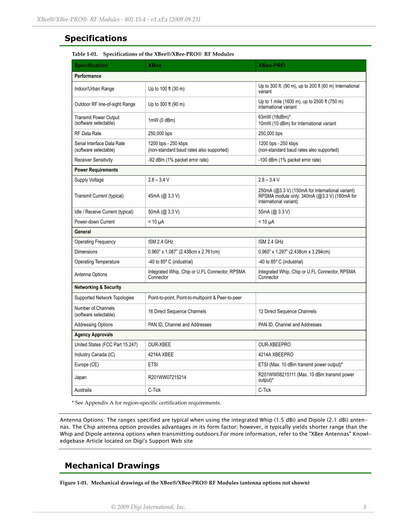
XBee®/XBee‐PRO® RF Modules ‐ 802.15.4 ‐ v1.xEx [2009.09.23]
© 2009 Digi Internatonal, Inc. 5
Specifications
* See Appendix A for region‐specific certification requirements.
Antenna Options: The ranges specified are typical when using the integrated Whip (1.5 dBi) and Dipole (2.1 dBi) anten-nas. The Chip antenna option provides advantages in its form factor; however, it typically yields shorter range than the Whip and Dipole antenna options when transmitting outdoors.For more information, refer to the "XBee Antennas" Knowl-edgebase Article located on Digi's Support Web site
Mechanical Drawings
Figure 1‐01. Mechanical drawings of the XBee®/XBee‐PRO® RF Modules (antenna options not shown)
Table 1‐01. Specifications of the XBee®/XBee‐PRO® RF Modules
Specification XBee XBee-PRO
Performance
Indoor/Urban Range Up to 100 ft (30 m) Up to 300 ft. (90 m), up to 200 ft (60 m) International variant
Outdoor RF line-of-sight Range Up to 300 ft (90 m) Up to 1 mile (1600 m), up to 2500 ft (750 m) international variant
Transmit Power Output (software selectable) 1mW (0 dBm) 63mW (18dBm)*
10mW (10 dBm) for International variant
RF Data Rate 250,000 bps 250,000 bps
Serial Interface Data Rate(software selectable)
1200 bps - 250 kbps(non-standard baud rates also supported)
1200 bps - 250 kbps(non-standard baud rates also supported)
Receiver Sensitivity -92 dBm (1% packet error rate) -100 dBm (1% packet error rate)
Power Requirements
Supply Voltage 2.8 – 3.4 V 2.8 – 3.4 V
Transmit Current (typical) 45mA (@ 3.3 V)250mA (@3.3 V) (150mA for international variant) RPSMA module only: 340mA (@3.3 V) (180mA for international variant)
Idle / Receive Current (typical) 50mA (@ 3.3 V) 55mA (@ 3.3 V)
Power-down Current < 10 µA < 10 µA
General
Operating Frequency ISM 2.4 GHz ISM 2.4 GHz
Dimensions 0.960” x 1.087” (2.438cm x 2.761cm) 0.960” x 1.297” (2.438cm x 3.294cm)
Operating Temperature -40 to 85º C (industrial) -40 to 85º C (industrial)
Antenna Options Integrated Whip, Chip or U.FL Connector, RPSMA Connector
Integrated Whip, Chip or U.FL Connector, RPSMA Connector
Networking & Security
Supported Network Topologies Point-to-point, Point-to-multipoint & Peer-to-peer
Number of Channels(software selectable) 16 Direct Sequence Channels 12 Direct Sequence Channels
Addressing Options PAN ID, Channel and Addresses PAN ID, Channel and Addresses
Agency Approvals
United States (FCC Part 15.247) OUR-XBEE OUR-XBEEPRO
Industry Canada (IC) 4214A XBEE 4214A XBEEPRO
Europe (CE) ETSI ETSI (Max. 10 dBm transmit power output)*
Japan R201WW07215214 R201WW08215111 (Max. 10 dBm transmit power output)*
Austraila C-Tick C-Tick
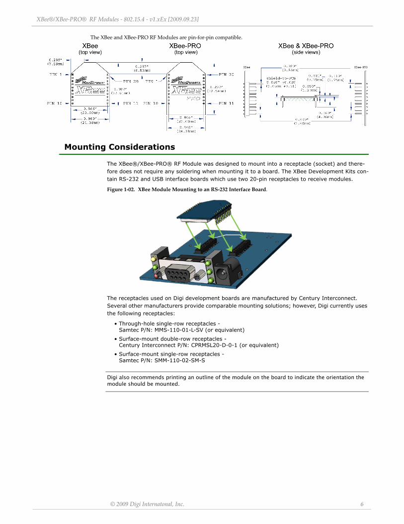
XBee®/XBee‐PRO® RF Modules ‐ 802.15.4 ‐ v1.xEx [2009.09.23]
© 2009 Digi Internatonal, Inc. 6
The XBee and XBee‐PRO RF Modules are pin‐for‐pin compatible.
Mounting Considerations
The XBee®/XBee-PRO® RF Module was designed to mount into a receptacle (socket) and there-fore does not require any soldering when mounting it to a board. The XBee Development Kits con-tain RS-232 and USB interface boards which use two 20-pin receptacles to receive modules.
Figure 1‐02. XBee Module Mounting to an RS‐232 Interface Board.
The receptacles used on Digi development boards are manufactured by Century Interconnect. Several other manufacturers provide comparable mounting solutions; however, Digi currently uses the following receptacles:
• Through-hole single-row receptacles - Samtec P/N: MMS-110-01-L-SV (or equivalent)
• Surface-mount double-row receptacles - Century Interconnect P/N: CPRMSL20-D-0-1 (or equivalent)
• Surface-mount single-row receptacles - Samtec P/N: SMM-110-02-SM-S
Digi also recommends printing an outline of the module on the board to indicate the orientation the module should be mounted.
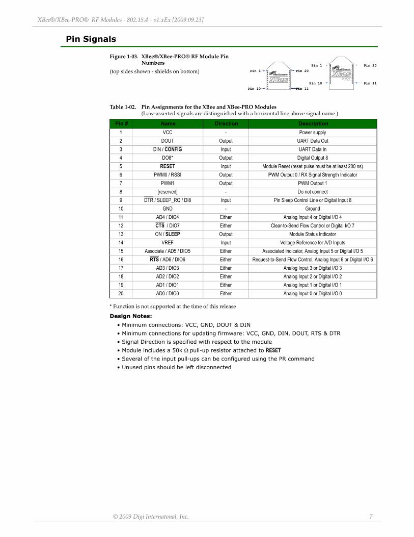
XBee®/XBee‐PRO® RF Modules ‐ 802.15.4 ‐ v1.xEx [2009.09.23]
© 2009 Digi Internatonal, Inc. 7
Pin Signals
Figure 1‐03. XBee®/XBee‐PRO® RF Module Pin Numbers
(top sides shown ‐ shields on bottom)
* Function is not supported at the time of this release
Design Notes:
• Minimum connections: VCC, GND, DOUT & DIN
• Minimum connections for updating firmware: VCC, GND, DIN, DOUT, RTS & DTR
• Signal Direction is specified with respect to the module
• Module includes a 50k Ω pull-up resistor attached to RESET• Several of the input pull-ups can be configured using the PR command
• Unused pins should be left disconnected
Table 1‐02. Pin Assignments for the XBee and XBee‐PRO Modules (Low‐asserted signals are distinguished with a horizontal line above signal name.)
Pin # Name Direction Description1 VCC - Power supply2 DOUT Output UART Data Out3 DIN / CONFIG Input UART Data In4 DO8* Output Digital Output 85 RESET Input Module Reset (reset pulse must be at least 200 ns)6 PWM0 / RSSI Output PWM Output 0 / RX Signal Strength Indicator7 PWM1 Output PWM Output 18 [reserved] - Do not connect9 DTR / SLEEP_RQ / DI8 Input Pin Sleep Control Line or Digital Input 810 GND - Ground11 AD4 / DIO4 Either Analog Input 4 or Digital I/O 412 CTS / DIO7 Either Clear-to-Send Flow Control or Digital I/O 713 ON / SLEEP Output Module Status Indicator14 VREF Input Voltage Reference for A/D Inputs15 Associate / AD5 / DIO5 Either Associated Indicator, Analog Input 5 or Digital I/O 516 RTS / AD6 / DIO6 Either Request-to-Send Flow Control, Analog Input 6 or Digital I/O 617 AD3 / DIO3 Either Analog Input 3 or Digital I/O 318 AD2 / DIO2 Either Analog Input 2 or Digital I/O 219 AD1 / DIO1 Either Analog Input 1 or Digital I/O 120 AD0 / DIO0 Either Analog Input 0 or Digital I/O 0
Pin 1
Pin 10
Pin 1
Pin 10
Pin 20
Pin 11
Pin 20
Pin 11
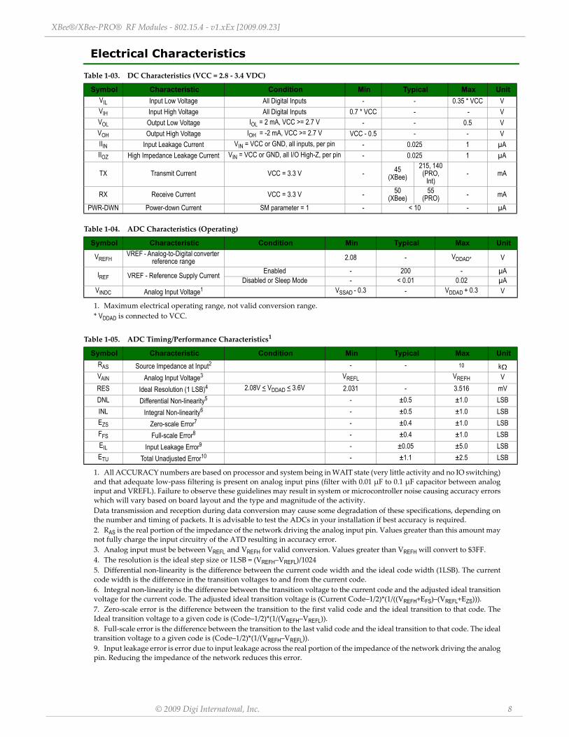
XBee®/XBee‐PRO® RF Modules ‐ 802.15.4 ‐ v1.xEx [2009.09.23]
© 2009 Digi Internatonal, Inc. 8
Electrical Characteristics
Table 1‐03. DC Characteristics (VCC = 2.8 ‐ 3.4 VDC)
Symbol Characteristic Condition Min Typical Max UnitVIL Input Low Voltage All Digital Inputs - - 0.35 * VCC VVIH Input High Voltage All Digital Inputs 0.7 * VCC - - VVOL Output Low Voltage IOL = 2 mA, VCC >= 2.7 V - - 0.5 VVOH Output High Voltage IOH = -2 mA, VCC >= 2.7 V VCC - 0.5 - - VIIIN Input Leakage Current VIN = VCC or GND, all inputs, per pin - 0.025 1 µAIIOZ High Impedance Leakage Current VIN = VCC or GND, all I/O High-Z, per pin - 0.025 1 µA
TX Transmit Current VCC = 3.3 V - 45(XBee)
215, 140 (PRO,
Int)- mA
RX Receive Current VCC = 3.3 V - 50(XBee)
55(PRO) - mA
PWR-DWN Power-down Current SM parameter = 1 - < 10 - µA
Table 1‐04. ADC Characteristics (Operating)
Symbol Characteristic Condition Min Typical Max Unit
VREFHVREF - Analog-to-Digital converter
reference range 2.08 - VDDAD* V
IREF VREF - Reference Supply Current Enabled - 200 - µADisabled or Sleep Mode - < 0.01 0.02 µA
VINDC Analog Input Voltage1
1. Maximum electrical operating range, not valid conversion range. * VDDAD is connected to VCC.
VSSAD - 0.3 - VDDAD + 0.3 V
Table 1‐05. ADC Timing/Performance Characteristics1
1. All ACCURACY numbers are based on processor and system being in WAIT state (very little activity and no IO switching) and that adequate low‐pass filtering is present on analog input pins (filter with 0.01 μF to 0.1 μF capacitor between analog input and VREFL). Failure to observe these guidelines may result in system or microcontroller noise causing accuracy errors which will vary based on board layout and the type and magnitude of the activity.Data transmission and reception during data conversion may cause some degradation of these specifications, depending on the number and timing of packets. It is advisable to test the ADCs in your installation if best accuracy is required.
Symbol Characteristic Condition Min Typical Max UnitRAS Source Impedance at Input2
2. RAS is the real portion of the impedance of the network driving the analog input pin. Values greater than this amount may not fully charge the input circuitry of the ATD resulting in accuracy error.
- - 10 kVAIN Analog Input Voltage3
3. Analog input must be between VREFL and VREFH for valid conversion. Values greater than VREFH will convert to $3FF.
VREFL VREFH VRES Ideal Resolution (1 LSB)4
4. The resolution is the ideal step size or 1LSB = (VREFH–VREFL)/1024
2.08V < VDDAD < 3.6V 2.031 - 3.516 mVDNL Differential Non-linearity5
5. Differential non‐linearity is the difference between the current code width and the ideal code width (1LSB). The current code width is the difference in the transition voltages to and from the current code.
- ±0.5 ±1.0 LSBINL Integral Non-linearity6
6. Integral non‐linearity is the difference between the transition voltage to the current code and the adjusted ideal transition voltage for the current code. The adjusted ideal transition voltage is (Current Code–1/2)*(1/((VREFH+EFS)–(VREFL+EZS))).
- ±0.5 ±1.0 LSBEZS Zero-scale Error7
7. Zero‐scale error is the difference between the transition to the first valid code and the ideal transition to that code. The Ideal transition voltage to a given code is (Code–1/2)*(1/(VREFH–VREFL)).
- ±0.4 ±1.0 LSBFFS Full-scale Error8
8. Full‐scale error is the difference between the transition to the last valid code and the ideal transition to that code. The ideal transition voltage to a given code is (Code–1/2)*(1/(VREFH–VREFL)).
- ±0.4 ±1.0 LSBEIL Input Leakage Error9
9. Input leakage error is error due to input leakage across the real portion of the impedance of the network driving the analog pin. Reducing the impedance of the network reduces this error.
- ±0.05 ±5.0 LSBETU Total Unadjusted Error10 - ±1.1 ±2.5 LSB

XBee®/XBee‐PRO® RF Modules ‐ 802.15.4 ‐ v1.xEx [2009.09.23]
© 2009 Digi Internatonal, Inc. 9
10.Total unadjusted error is the difference between the transition voltage to the current code and the ideal straight‐line trans‐fer function. This measure of error includes inherent quantization error (1/2LSB) and circuit error (differential, integral, zero‐scale, and full‐scale) error. The specified value of ETU assumes zero EIL (no leakage or zero real source impedance).
© 2009 Digi International Inc. 10
2. RF Module Operation
Serial Communications
The XBee®/XBee-PRO® RF Modules interface to a host device through a logic-level asynchronous serial port. Through its serial port, the module can communicate with any logic and voltage com-patible UART; or through a level translator to any serial device (For example: Through a Digi pro-prietary RS-232 or USB interface board).
UART Data Flow
Devices that have a UART interface can connect directly to the pins of the RF module as shown in the figure below.
Figure 2‐01. System Data Flow Diagram in a UART‐interfaced environment (Low‐asserted signals distinguished with horizontal line over signal name.)
Serial Data
Data enters the module UART through the DI pin (pin 3) as an asynchronous serial signal. The sig-nal should idle high when no data is being transmitted.
Each data byte consists of a start bit (low), 8 data bits (least significant bit first) and a stop bit (high). The following figure illustrates the serial bit pattern of data passing through the module.
Figure 2‐02. UART data packet 0x1F (decimal number ʺ31ʺ) as transmitted through the RF module Example Data Format is 8‐N‐1 (bits ‐ parity ‐ # of stop bits)
Serial communications depend on the two UARTs (the microcontroller's and the RF module's) to be configured with compatible settings (baud rate, parity, start bits, stop bits, data bits).
The UART baud rate and parity settings on the XBee module can be configured with the BD and SB commands, respectively. See the command table in Chapter 3 for details.
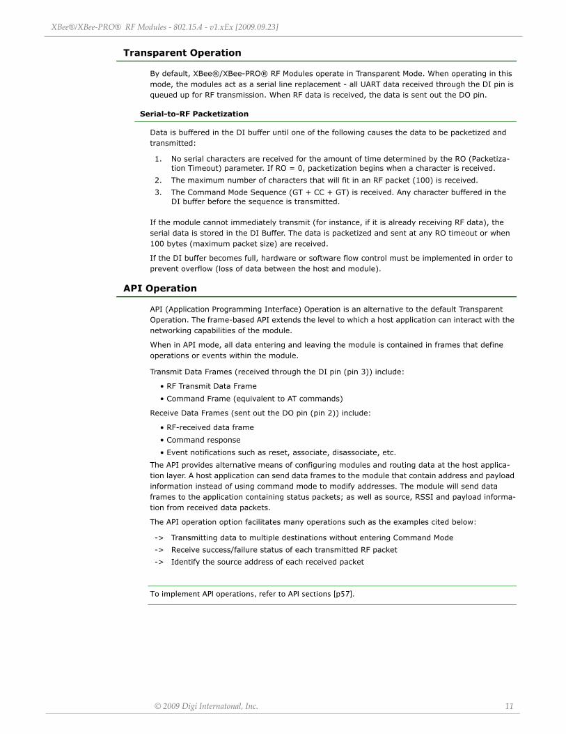
XBee®/XBee‐PRO® RF Modules ‐ 802.15.4 ‐ v1.xEx [2009.09.23]
© 2009 Digi Internatonal, Inc. 11
Transparent Operation
By default, XBee®/XBee-PRO® RF Modules operate in Transparent Mode. When operating in this mode, the modules act as a serial line replacement - all UART data received through the DI pin is queued up for RF transmission. When RF data is received, the data is sent out the DO pin.
Serial-to-RF Packetization
Data is buffered in the DI buffer until one of the following causes the data to be packetized and transmitted:
If the module cannot immediately transmit (for instance, if it is already receiving RF data), the serial data is stored in the DI Buffer. The data is packetized and sent at any RO timeout or when 100 bytes (maximum packet size) are received.
If the DI buffer becomes full, hardware or software flow control must be implemented in order to prevent overflow (loss of data between the host and module).
API Operation
API (Application Programming Interface) Operation is an alternative to the default Transparent Operation. The frame-based API extends the level to which a host application can interact with the networking capabilities of the module.
When in API mode, all data entering and leaving the module is contained in frames that define operations or events within the module.
Transmit Data Frames (received through the DI pin (pin 3)) include:
• RF Transmit Data Frame
• Command Frame (equivalent to AT commands)
Receive Data Frames (sent out the DO pin (pin 2)) include:
• RF-received data frame
• Command response
• Event notifications such as reset, associate, disassociate, etc.
The API provides alternative means of configuring modules and routing data at the host applica-tion layer. A host application can send data frames to the module that contain address and payload information instead of using command mode to modify addresses. The module will send data frames to the application containing status packets; as well as source, RSSI and payload informa-tion from received data packets.
The API operation option facilitates many operations such as the examples cited below:
To implement API operations, refer to API sections [p57].
1. No serial characters are received for the amount of time determined by the RO (Packetiza-tion Timeout) parameter. If RO = 0, packetization begins when a character is received.
2. The maximum number of characters that will fit in an RF packet (100) is received.
3. The Command Mode Sequence (GT + CC + GT) is received. Any character buffered in the DI buffer before the sequence is transmitted.
-> Transmitting data to multiple destinations without entering Command Mode
-> Receive success/failure status of each transmitted RF packet
-> Identify the source address of each received packet
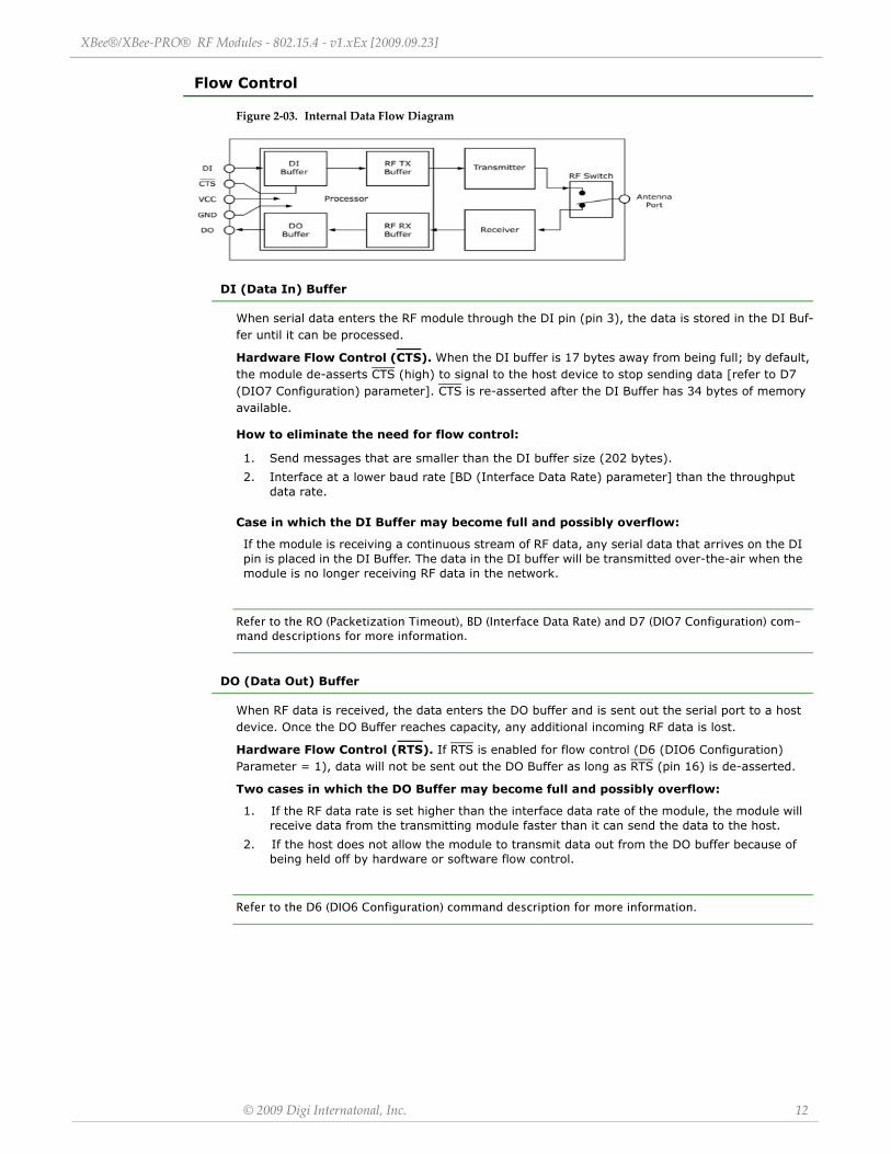
XBee®/XBee‐PRO® RF Modules ‐ 802.15.4 ‐ v1.xEx [2009.09.23]
© 2009 Digi Internatonal, Inc. 12
Flow Control
Figure 2‐03. Internal Data Flow Diagram
DI (Data In) Buffer
When serial data enters the RF module through the DI pin (pin 3), the data is stored in the DI Buf-fer until it can be processed.
Hardware Flow Control (CTS). When the DI buffer is 17 bytes away from being full; by default, the module de-asserts CTS (high) to signal to the host device to stop sending data [refer to D7 (DIO7 Configuration) parameter]. CTS is re-asserted after the DI Buffer has 34 bytes of memory available.
How to eliminate the need for flow control:
Case in which the DI Buffer may become full and possibly overflow:
Refer to the RO (Packetization Timeout), BD (Interface Data Rate) and D7 (DIO7 Configuration) com-mand descriptions for more information.
DO (Data Out) Buffer
When RF data is received, the data enters the DO buffer and is sent out the serial port to a host device. Once the DO Buffer reaches capacity, any additional incoming RF data is lost.
Hardware Flow Control (RTS). If RTS is enabled for flow control (D6 (DIO6 Configuration) Parameter = 1), data will not be sent out the DO Buffer as long as RTS (pin 16) is de-asserted.
Two cases in which the DO Buffer may become full and possibly overflow:
Refer to the D6 (DIO6 Configuration) command description for more information.
1. Send messages that are smaller than the DI buffer size (202 bytes).
2. Interface at a lower baud rate [BD (Interface Data Rate) parameter] than the throughput data rate.
If the module is receiving a continuous stream of RF data, any serial data that arrives on the DI pin is placed in the DI Buffer. The data in the DI buffer will be transmitted over-the-air when the module is no longer receiving RF data in the network.
1. If the RF data rate is set higher than the interface data rate of the module, the module will receive data from the transmitting module faster than it can send the data to the host.
2. If the host does not allow the module to transmit data out from the DO buffer because of being held off by hardware or software flow control.
XBee®/XBee‐PRO® RF Modules ‐ 802.15.4 ‐ v1.xEx [2009.09.23]
© 2009 Digi Internatonal, Inc. 13
ADC and Digital I/O Line Support
The XBee®/XBee-PRO® RF Modules support ADC (Analog-to-digital conversion) and digital I/O line passing. The following pins support multiple functions:
To enable ADC and DIO pin functions:
I/O Data Format
I/O data begins with a header. The first byte of the header defines the number of samples forth-coming. The last 2 bytes of the header (Channel Indicator) define which inputs are active. Each bit represents either a DIO line or ADC channel.
Figure 2‐04. Header
Sample data follows the header and the channel indicator frame is used to determine how to read the sample data. If any of the DIO lines are enabled, the first 2 bytes are the DIO sample. The ADC data follows. ADC channel data is represented as an unsigned 10-bit value right-justified on a 16- bit boundary.
Figure 2‐05. Sample Data
Table 2‐01. Pin functions and their associated pin numbers and commands AD = Analog‐to‐Digital Converter, DIO = Digital Input/Output Pin functions not applicable to this section are denoted within (parenthesis).
Pin Function Pin# AT CommandAD0 / DIO0 20 D0AD1 / DIO1 19 D1AD2 / DIO2 18 D2AD3 / DIO3 / (COORD_SEL) 17 D3AD4 / DIO4 11 D4AD5 / DIO5 / (ASSOCIATE) 15 D5DIO6 / (RTS) 16 D6DIO7 / (CTS) 12 D7DI8 / (DTR) / (Sleep_RQ) 9 D8
For ADC Support: Set ATDn = 2
For Digital Input support: Set ATDn = 3
For Digital Output Low support: Set ATDn = 4
For Digital Output High support: Set ATDn = 5
Header
Bit set to ‘1’ if channel is active
Bytes 2 - 3 (Channel Indicator)
na D8A0A1A2A3A4A5 D7 D0D1D2D3D4D5D6
Byte 1
Total number of samples
bit 15 bit 0
Sample DataDIO Line Data is first (if enabled) ADC Line Data
ADCn MSB ADCn LSB7 0123456X 8XXXXXX
XBee®/XBee‐PRO® RF Modules ‐ 802.15.4 ‐ v1.xEx [2009.09.23]
© 2009 Digi Internatonal, Inc. 14
API Support
I/O data is sent out the UART using an API frame. All other data can be sent and received using Transparent Operation [refer to p11] or API framing if API mode is enabled (AP > 0).
API Operations support two RX (Receive) frame identifiers for I/O data (set 16-bit address to 0xFFFE and the module will do 64-bit addressing):
• 0x82 for RX (Receive) Packet: 64-bit address I/O
• 0x83 for RX (Receive) Packet: 16-bit address I/O
The API command header is the same as shown in the “RX (Receive) Packet: 64-bit Address” and “RX (Receive) Packet: 64-bit Address” API types [refer to p63]. RX data follows the format described in the I/O Data Format section [p13].
Applicable Commands: AP (API Enable)
Sleep Support
Automatic wakeup sampling can be suppressed by setting SO bit 1.When an RF module wakes, it will always do a sample based on any active ADC or DIO lines. This allows sampling based on the sleep cycle whether it be Cyclic Sleep (SM parameter = 4 or 5) or Pin Sleep (SM = 1 or 2). To gather more samples when awake, set the IR (Sample Rate) parameter.
For Cyclic Sleep modes: If the IR parameter is set, the module will stay awake until the IT (Sam-ples before TX) parameter is met. The module will stay awake for ST (Time before Sleep) time.
Applicable Commands: IR (Sample Rate), IT (Samples before TX), SM (Sleep Mode), IC (DIO Change Detect), SO (Sleep Options)
DIO Pin Change Detect
When “DIO Change Detect” is enabled (using the IC command), DIO lines 0-7 are monitored. When a change is detected on a DIO line, the following will occur:
Note: Change detect will not affect Pin Sleep wake-up. The D8 pin (DTR/Sleep_RQ/DI8) is the only line that will wake a module from Pin Sleep. If not all samples are collected, the module will still enter Sleep Mode after a change detect packet is sent.
Applicable Commands: IC (DIO Change Detect), IT (Samples before TX)
NOTE: Change detect is only supported when the Dx (DIOx Configuration) parameter equals 3,4 or 5.
Sample Rate (Interval)
The Sample Rate (Interval) feature allows enabled ADC and DIO pins to be read periodically on modules that are not configured to operate in Sleep Mode. When one of the Sleep Modes is enabled and the IR (Sample Rate) parameter is set, the module will stay awake until IT (Samples before TX) samples have been collected.
Once a particular pin is enabled, the appropriate sample rate must be chosen. The maximum sam-ple rate that can be achieved while using one A/D line is 1 sample/ms or 1 KHz (Note that the modem will not be able to keep up with transmission when IR & IT are equal to “1” and that con-figuring the modem to sample at rates greater than once every 20ms is not recommended).
Applicable Commands: IR (Sample Rate), IT (Samples before TX), SM (Sleep Mode)
1. An RF packet is sent with the updated DIO pin levels. This packet will not contain any ADC samples.
2. Any queued samples are transmitted before the change detect data. This may result in receiving a packet with less than IT (Samples before TX) samples.
XBee®/XBee‐PRO® RF Modules ‐ 802.15.4 ‐ v1.xEx [2009.09.23]
© 2009 Digi Internatonal, Inc. 15
I/O Line Passing
Virtual wires can be set up between XBee®/XBee-PRO® Modules. When an RF data packet is received that contains I/O data, the receiving module can be setup to update any enabled outputs (PWM and DIO) based on the data it receives.
Note that I/O lines are mapped in pairs. For example: AD0 can only update PWM0 and DI5 can only update DO5. The default setup is for outputs not to be updated, which results in the I/O data being sent out the UART (refer to the IU (Enable I/O Output) command). To enable the outputs to be updated, the IA (I/O Input Address) parameter must be setup with the address of the module that has the appropriate inputs enabled. This effectively binds the outputs to a particular module’s input. This does not affect the ability of the module to receive I/O line data from other modules - only its ability to update enabled outputs. The IA parameter can also be setup to accept I/O data for output changes from any module by setting the IA parameter to 0xFFFF.
When outputs are changed from their non-active state, the module can be setup to return the out-put level to it non-active state. The timers are set using the Tn (Dn Output Timer) and PT (PWM Output Timeout) commands. The timers are reset every time a valid I/O packet (passed IA check) is received. The IC (Change Detect) and IR (Sample Rate) parameters can be setup to keep the output set to their active output if the system needs more time than the timers can handle.
Note: DI8 cannot be used for I/O line passing.
Applicable Commands: IA (I/O Input Address), Tn (Dn Output Timeout), P0 (PWM0 Configura-tion), P1 (PWM1 Configuration), M0 (PWM0 Output Level), M1 (PWM1 Output Level), PT (PWM Output Timeout), RP (RSSSI PWM Timer)
Configuration Example
As an example for a simple A/D link, a pair of RF modules could be set as follows:
These settings configure the remote module to sample AD0 and AD1 once each every 20 ms. It then buffers 5 samples each before sending them back to the base module. The base should then receive a 32-Byte transmission (20 Bytes data and 12 Bytes framing) every 100 ms.
Remote ConfigurationDL = 0x1234MY = 0x5678
D0 = 2D1 = 2
IR = 0x14IT = 5
Base ConfigurationDL = 0x5678MY = 0x1234
P0 = 2P1 = 2IU = 1
IA = 0x5678 (or 0xFFFF)
XBee®/XBee‐PRO® RF Modules ‐ 802.15.4 ‐ v1.xEx [2009.09.23]
© 2009 Digi Internatonal, Inc. 16
XBee®/XBee-PRO® Networks
The following terms will be used to explicate the network operations:
Peer-to-Peer
By default, XBee®/XBee-PRO RF Modules are configured to operate within a Peer-to-Peer network topology and therefore are not dependent upon Master/Slave relationships. NonBeacon systems operate within a Peer-to-Peer network topology and therefore are not dependent upon Master/Slave relationships. This means that modules remain synchronized without use of master/server configurations and each module in the network shares both roles of master and slave. Digi's peer-to-peer architecture features fast synchronization times and fast cold start times. This default con-figuration accommodates a wide range of RF data applications.
Figure 2‐06. Peer‐to‐Peer Architecture
A peer-to-peer network can be established by configuring each module to operate as an End Device (CE = 0), disabling End Device Association on all modules (A1 = 0) and setting ID and CH parameters to be identical across the network.
NonBeacon (w/ Coordinator)
A device is configured as a Coordinator by setting the CE (Coordinator Enable) parameter to “1”. Coordinator power-up is governed by the A2 (Coordinator Association) parameter.
In a Coordinator system, the Coordinator can be configured to use direct or indirect transmissions. If the SP (Cyclic Sleep Period) parameter is set to “0”, the Coordinator will send data immediately. Otherwise, the SP parameter determines the length of time the Coordinator will retain the data before discarding it. Generally, SP (Cyclic Sleep Period) and ST (Time before Sleep) parameters should be set to match the SP and ST settings of the End Devices.
Table 2‐02. Terms and definitions
Term Definition
PAN Personal Area Network - A data communication network that includes one or more End Devices and optionally a Coordinator.
Coordinator A Full-function device (FFD) that provides network synchronization by polling nodes [NonBeacon (w/ Coordinator) networks only]
End Device When in the same network as a Coordinator - RF modules that rely on a Coordinator for synchronization and can be put into states of sleep for low-power applications.
Association The establishment of membership between End Devices and a Coordinator. Association is only applicable in NonBeacon (w/Coordinator) networks.
XBee®/XBee‐PRO® RF Modules ‐ 802.15.4 ‐ v1.xEx [2009.09.23]
© 2009 Digi Internatonal, Inc. 17
Association
Association is the establishment of membership between End Devices and a Coordinator. The establishment of membership is useful in scenarios that require a central unit (Coordinator) to relay messages to or gather data from several remote units (End Devices), assign channels or assign PAN IDs.
An RF data network that consists of one Coordinator and one or more End Devices forms a PAN (Personal Area Network). Each device in a PAN has a PAN Identifier [ID (PAN ID) parameter]. PAN IDs must be unique to prevent miscommunication between PANs. The Coordinator PAN ID is set using the ID (PAN ID) and A2 (Coordinator Association) commands.
An End Device can associate to a Coordinator without knowing the address, PAN ID or channel of the Coordinator. The A1 (End Device Association) parameter bit fields determine the flexibility of an End Device during association. The A1 parameter can be used for an End Device to dynamically set its destination address, PAN ID and/or channel.
Coordinator / End Device Setup and Operation
To configure a module to operate as a Coordinator, set the CE (Coordinator Enable) parameter to ‘1’. Set the CE parameter of End Devices to ‘0’ (default). Coordinator and End Devices should con-tain matching firmware versions.
NonBeacon (w/ Coordinator) Systems
The Coordinator can be configured to use direct or indirect transmissions. If the SP (Cyclic Sleep Period) parameter is set to ‘0’, the Coordinator will send data immediately. Otherwise, the SP parameter determines the length of time the Coordinator will retain the data before discarding it. Generally, SP (Cyclic Sleep Period) and ST (Time before Sleep) parameters should be set to match the SP and ST settings of the End Devices.
Coordinator Start-up
Coordinator power-up is governed by the A2 (Coordinator Association) command. On power-up, the Coordinator undergoes the following sequence of events:
1. Check A2 parameter- Reassign_PANID Flag
Set (bit 0 = 1) - The Coordinator issues an Active Scan. The Active Scan selects one channel and transmits a request to the broadcast address (0xFFFF) and broadcast PAN ID (0xFFFF). It then listens on that channel for beacons from any Coordinator operating on that channel. The listen time on each channel is determined by the SD (Scan Duration) parameter value.
Once the time expires on that channel, the Active Scan selects another channel and again transmits the BeaconRequest as before. This process continues until all channels have been scanned, or until 5 PANs have been discovered. When the Active Scan is complete, the results include a list of PAN IDs and Channels that are being used by other PANs. This list is used to assign an unique PAN ID to the new Coordinator. The ID parameter will be retained if it is not found in the Active Scan results. Otherwise, the ID (PAN ID) parameter setting will be updated to a PAN ID that was not detected.
Not Set (bit 0 = 0) - The Coordinator retains its ID setting. No Active Scan is performed.
For example: If the PAN ID of a Coordinator is known, but the operating channel is not; the A1 command on the End Device should be set to enable the ‘Auto_Associate’ and ‘Reassign_Channel’ bits. Additionally, the ID parameter should be set to match the PAN ID of the associated Coordinator.
XBee®/XBee‐PRO® RF Modules ‐ 802.15.4 ‐ v1.xEx [2009.09.23]
© 2009 Digi Internatonal, Inc. 18
2. Check A2 parameter - Reassign_Channel Flag (bit 1)
Set (bit 1 = 1) - The Coordinator issues an Energy Scan. The Energy Scan selects one channel and scans for energy on that channel. The duration of the scan is specified by the SD (Scan Duration) parameter. Once the scan is completed on a channel, the Energy Scan selects the next channel and begins a new scan on that channel. This process continues until all channels have been scanned.
When the Energy Scan is complete, the results include the maximal energy values detected on each channel. This list is used to determine a channel where the least energy was detected. If an Active Scan was performed (Reassign_PANID Flag set), the channels used by the detected PANs are eliminated as possible channels. Thus, the results of the Energy Scan and the Active Scan (if performed) are used to find the best channel (channel with the least energy that is not used by any detected PAN). Once the best channel has been selected, the CH (Channel) param-eter value is updated to that channel.
Not Set (bit 1 = 0) - The Coordinator retains its CH setting. An Energy Scan is not performed.
3. Start Coordinator
The Coordinator starts on the specified channel (CH parameter) and PAN ID (ID parameter). Note, these may be selected in steps 1 and/or 2 above. The Coordinator will only allow End Devices to associate to it if the A2 parameter “AllowAssociation” flag is set. Once the Coordina-tor has successfully started, the Associate LED will blink 1 time per second. (The LED is solid if the Coordinator has not started.)
4. Coordinator Modifications
Once a Coordinator has started: Modifying the A2 (Reassign_Channel or Reassign_PANID bits), ID, CH or MY parameters will cause the Coordinator’s MAC to reset (The Coordinator RF module (including volatile RAM) is not reset). Changing the A2 AllowAssociation bit will not reset the Coordinator’s MAC. In a non-beaconing system, End Devices that associated to the Coordinator prior to a MAC reset will have knowledge of the new settings on the Coordinator. Thus, if the Coordinator were to change its ID, CH or MY settings, the End Devices would no longer be able to communicate with the non-beacon Coordinator. Once a Coordinator has started, the ID, CH, MY or A2 (Reassign_Channel or Reassign_PANID bits) should not be changed.
End Device Start-up
End Device power-up is governed by the A1 (End Device Association) command. On power-up, the End Device undergoes the following sequence of events:
1. Check A1 parameter - AutoAssociate Bit
Set (bit 2 = 1) - End Device will attempt to associate to a Coordinator. (refer to steps 2-3).
Not Set (bit 2 = 0) - End Device will not attempt to associate to a Coordinator. The End Device will operate as specified by its ID, CH and MY parameters. Association is considered complete and the Associate LED will blink quickly (5 times per second). When the AutoAssociate bit is not set, the remaining steps (2-3) do not apply.
2. Discover Coordinator (if Auto-Associate Bit Set)
The End Device issues an Active Scan. The Active Scan selects one channel and transmits a BeaconRequest command to the broadcast address (0xFFFF) and broadcast PAN ID (0xFFFF). It then listens on that channel for beacons from any Coordinator operating on that channel. The listen time on each channel is determined by the SD parameter.
Once the time expires on that channel, the Active Scan selects another channel and again transmits the BeaconRequest command as before. This process continues until all channels have been scanned, or until 5 PANs have been discovered. When the Active Scan is complete, the results include a list of PAN IDs and Channels that are being used by detected PANs.
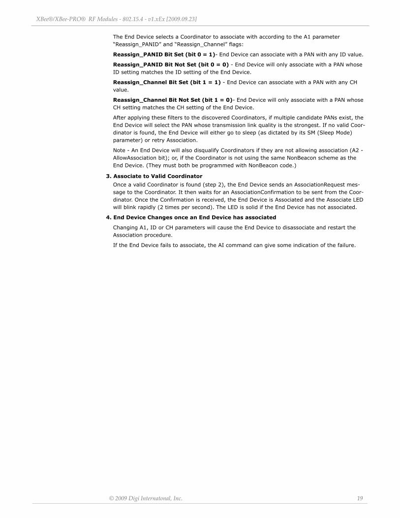
XBee®/XBee‐PRO® RF Modules ‐ 802.15.4 ‐ v1.xEx [2009.09.23]
© 2009 Digi Internatonal, Inc. 19
The End Device selects a Coordinator to associate with according to the A1 parameter “Reassign_PANID” and “Reassign_Channel” flags:
Reassign_PANID Bit Set (bit 0 = 1)- End Device can associate with a PAN with any ID value.
Reassign_PANID Bit Not Set (bit 0 = 0) - End Device will only associate with a PAN whose ID setting matches the ID setting of the End Device.
Reassign_Channel Bit Set (bit 1 = 1) - End Device can associate with a PAN with any CH value.
Reassign_Channel Bit Not Set (bit 1 = 0)- End Device will only associate with a PAN whose CH setting matches the CH setting of the End Device.
After applying these filters to the discovered Coordinators, if multiple candidate PANs exist, the End Device will select the PAN whose transmission link quality is the strongest. If no valid Coor-dinator is found, the End Device will either go to sleep (as dictated by its SM (Sleep Mode) parameter) or retry Association.
Note - An End Device will also disqualify Coordinators if they are not allowing association (A2 - AllowAssociation bit); or, if the Coordinator is not using the same NonBeacon scheme as the End Device. (They must both be programmed with NonBeacon code.)
3. Associate to Valid Coordinator
Once a valid Coordinator is found (step 2), the End Device sends an AssociationRequest mes-sage to the Coordinator. It then waits for an AssociationConfirmation to be sent from the Coor-dinator. Once the Confirmation is received, the End Device is Associated and the Associate LED will blink rapidly (2 times per second). The LED is solid if the End Device has not associated.
4. End Device Changes once an End Device has associated
Changing A1, ID or CH parameters will cause the End Device to disassociate and restart the Association procedure.
If the End Device fails to associate, the AI command can give some indication of the failure.
XBee®/XBee‐PRO® RF Modules ‐ 802.15.4 ‐ v1.xEx [2009.09.23]
© 2009 Digi Internatonal, Inc. 20
XBee®/XBee-PRO® Addressing
Every RF data packet sent over-the-air contains a Source Address and Destination Address field in its header. The RF module conforms to the 802.15.4 specification and supports both short 16-bit addresses and long 64-bit addresses. A unique 64-bit IEEE source address is assigned at the fac-tory and can be read with the SL (Serial Number Low) and SH (Serial Number High) commands. Short addressing must be configured manually. A module will use its unique 64-bit address as its Source Address if its MY (16-bit Source Address) value is “0xFFFF” or “0xFFFE”.
To send a packet to a specific module using 64-bit addressing: Set the Destination Address (DL + DH) of the sender to match the Source Address (SL + SH) of the intended destination module.
To send a packet to a specific module using 16-bit addressing: Set DL (Destination Address Low) parameter to equal the MY parameter of the intended destination module and set the DH (Destina-tion Address High) parameter to '0'.
Unicast Mode
By default, the RF module operates in Unicast Mode. Unicast Mode is the only mode that supports retries. While in this mode, receiving modules send an ACK (acknowledgement) of RF packet reception to the transmitter. If the transmitting module does not receive the ACK, it will re-send the packet up to three times or until the ACK is received.
Short 16-bit addresses. The module can be configured to use short 16-bit addresses as the Source Address by setting (MY < 0xFFFE). Setting the DH parameter (DH = 0) will configure the Destination Address to be a short 16-bit address (if DL < 0xFFFE). For two modules to communi-cate using short addressing, the Destination Address of the transmitter module must match the MY parameter of the receiver.
The following table shows a sample network configuration that would enable Unicast Mode com-munications using short 16-bit addresses.
Long 64-bit addresses. The RF module’s serial number (SL parameter concatenated to the SH parameter) can be used as a 64-bit source address when the MY (16-bit Source Address) parame-ter is disabled. When the MY parameter is disabled (MY = 0xFFFF or 0xFFFE), the module’s source address is set to the 64-bit IEEE address stored in the SH and SL parameters.
When an End Device associates to a Coordinator, its MY parameter is set to 0xFFFE to enable 64-bit addressing. The 64-bit address of the module is stored as SH and SL parameters. To send a packet to a specific module, the Destination Address (DL + DH) on the sender must match the Source Address (SL + SH) of the desired receiver.
Broadcast Mode
Any RF module within range will accept a packet that contains a broadcast address. When config-
ured to operate in Broadcast Mode, receiving modules do not send ACKs (Acknowledgements) and transmitting modules do not automatically re-send packets as is the case in Unicast Mode.
To send a broadcast packet to all modules regardless of 16-bit or 64-bit addressing, set the desti-nation addresses of all the modules as shown below.
Sample Network Configuration (All modules in the network):
• DL (Destination Low Address) = 0x0000FFFF
• DH (Destination High Address) = 0x00000000 (default value)
NOTE: When programming the module, parameters are entered in hexadecimal notation (without the “0x” prefix). Leading zeros may be omitted.
Table 2‐03. Sample Unicast Network Configuration (using 16‐bit addressing)
Parameter RF Module 1 RF Module 2MY (Source Address) 0x01 0x02
DH (Destination Address High) 0 0DL (Destination Address Low) 0x02 0x01
XBee®/XBee‐PRO® RF Modules ‐ 802.15.4 ‐ v1.xEx [2009.09.23]
© 2009 Digi Internatonal, Inc. 21
Modes of Operation
XBee®/XBee-PRO® RF Modules operate in five modes.
Figure 2‐07. Modes of Operation
Idle Mode
When not receiving or transmitting data, the RF module is in Idle Mode. The module shifts into the
other modes of operation under the following conditions:
• Transmit Mode (Serial data is received in the DI Buffer)
• Receive Mode (Valid RF data is received through the antenna)
• Sleep Mode (Sleep Mode condition is met)
• Command Mode (Command Mode Sequence is issued)
Transmit/Receive Modes
RF Data Packets
Each transmitted data packet contains a Source Address and Destination Address field. The Source Address matches the address of the transmitting module as specified by the MY (Source Address) parameter (if MY >= 0xFFFE), the SH (Serial Number High) parameter or the SL (Serial Number Low) parameter. The <Destination Address> field is created from the DH (Destination Address High) and DL (Destination Address Low) parameter values. The Source Address and/or Destination Address fields will either contain a 16-bit short or long 64-bit long address.
The RF data packet structure follows the 802.15.4 specification.
[Refer to the XBee/XBee-PRO Addressing section for more information]
Direct and Indirect Transmission
There are two methods to transmit data:
• Direct Transmission - data is transmitted immediately to the Destination Address
• Indirect Transmission - A packet is retained for a period of time and is only transmitted after the destination module (Source Address = Destination Address) requests the data.
Indirect Transmissions can only occur on a Coordinator. Thus, if all nodes in a network are End Devices, only Direct Transmissions will occur. Indirect Transmissions are useful to ensure packet delivery to a sleeping node. The Coordinator currently is able to retain up to 2 indirect messages.

XBee®/XBee‐PRO® RF Modules ‐ 802.15.4 ‐ v1.xEx [2009.09.23]
© 2009 Digi Internatonal, Inc. 22
Direct Transmission
A Coordinator can be configured to use only Direct Transmission by setting the SP (Cyclic Sleep Period) parameter to "0". Also, a Coordinator using indirect transmissions will revert to direct transmission if it knows the destination module is awake.
To enable this behavior, the ST (Time before Sleep) value of the Coordinator must be set to match the ST value of the End Device. Once the End Device either transmits data to the Coordinator or polls the Coordinator for data, the Coordinator will use direct transmission for all subsequent data transmissions to that module address until ST time occurs with no activity (at which point it will revert to using indirect transmissions for that module address). "No activity" means no transmis-sion or reception of messages with a specific address. Global messages will not reset the ST timer.
Indirect Transmission
To configure Indirect Transmissions in a PAN (Personal Area Network), the SP (Cyclic Sleep Period) parameter value on the Coordinator must be set to match the longest sleep value of any End Device. The sleep period value on the Coordinator determines how long (time or number of bea-cons) the Coordinator will retain an indirect message before discarding it.
An End Device must poll the Coordinator once it wakes from Sleep to determine if the Coordinator has an indirect message for it. For Cyclic Sleep Modes, this is done automatically every time the module wakes (after SP time). For Pin Sleep Modes, the A1 (End Device Association) parameter value must be set to enable Coordinator polling on pin wake-up. Alternatively, an End Device can use the FP (Force Poll) command to poll the Coordinator as needed.
CCA (Clear Channel Assessment)
Prior to transmitting a packet, a CCA (Clear Channel Assessment) is performed on the channel to determine if the channel is available for transmission. The detected energy on the channel is com-pared with the CA (Clear Channel Assessment) parameter value. If the detected energy exceeds the CA parameter value, the packet is not transmitted.
Also, a delay is inserted before a transmission takes place. This delay is settable using the RN (Backoff Exponent) parameter. If RN is set to “0”, then there is no delay before the first CCA is per-formed. The RN parameter value is the equivalent of the “minBE” parameter in the 802.15.4 spec-ification. The transmit sequence follows the 802.15.4 specification.
By default, the MM (MAC Mode) parameter = 0. On a CCA failure, the module will attempt to re-send the packet up to two additional times.
When in Unicast packets with RR (Retries) = 0, the module will execute two CCA retries. Broadcast packets always get two CCA retries.
Acknowledgement
If the transmission is not a broadcast message, the module will expect to receive an acknowledge-ment from the destination node. If an acknowledgement is not received, the packet will be resent up to 3 more times. If the acknowledgement is not received after all transmissions, an ACK failure is recorded.
XBee®/XBee‐PRO® RF Modules ‐ 802.15.4 ‐ v1.xEx [2009.09.23]
© 2009 Digi Internatonal, Inc. 23
Sleep Mode
Sleep Modes enable the RF module to enter states of low-power consumption when not in use. In order to enter Sleep Mode, one of the following conditions must be met (in addition to the module having a non-zero SM parameter value):
• Sleep_RQ (pin 9) is asserted and the module is in a pin sleep mode (SM = 1, 2, or 5)
• The module is idle (no data transmission or reception) for the amount of time defined by the ST (Time before Sleep) parameter. [NOTE: ST is only active when SM = 4-5.]
The SM command is central to setting Sleep Mode configurations. By default, Sleep Modes are dis-abled (SM = 0) and the module remains in Idle/Receive Mode. When in this state, the module is constantly ready to respond to serial or RF activity.
Pin/Host-controlled Sleep Modes
The transient current when waking from pin sleep (SM = 1 or 2) does not exceed the idle current of the module. The current ramps up exponentially to its idle current.
Pin Hibernate (SM = 1)• Pin/Host-controlled
• Typical power-down current: < 10 µA (@3.0 VCC)
• Wake-up time: 13.2 msec
Pin Hibernate Mode minimizes quiescent power (power consumed when in a state of rest or inac-tivity). This mode is voltage level-activated; when Sleep_RQ (pin 9) is asserted, the module will finish any transmit, receive or association activities, enter Idle Mode, and then enter a state of sleep. The module will not respond to either serial or RF activity while in pin sleep.
To wake a sleeping module operating in Pin Hibernate Mode, de-assert Sleep_RQ (pin 9). The module will wake when Sleep_RQ is de-asserted and is ready to transmit or receive when the CTS line is low. When waking the module, the pin must be de-asserted at least two 'byte times' after CTS goes low. This assures that there is time for the data to enter the DI buffer.
Pin Doze (SM = 2)• Pin/Host-controlled
• Typical power-down current: < 50 µA
• Wake-up time: 2 msec
Pin Doze Mode functions as does Pin Hibernate Mode; however, Pin Doze features faster wake-up
time and higher power consumption.
To wake a sleeping module operating in Pin Doze Mode, de-assert Sleep_RQ (pin 9). The module
will wake when Sleep_RQ is de-asserted and is ready to transmit or receive when the CTS line is
Table 2‐04. Sleep Mode Configurations
Sleep Mode Setting
Transition into Sleep Mode
Transition out of Sleep Mode (wake) Characteristics Related
CommandsPowerConsumption
Pin Hibernate (SM = 1)
Assert (high) Sleep_RQ (pin 9) De-assert (low) Sleep_RQ
Pin/Host-controlled / NonBeacon systems only / Lowest Power
(SM) < 10 µA (@3.0 VCC)
Pin Doze (SM = 2)
Assert (high) Sleep_RQ (pin 9) De-assert (low) Sleep_RQ
Pin/Host-controlled / NonBeacon systems only / Fastest wake-up
(SM) < 50 µA
Cyclic Sleep (SM = 4)
Automatic transition to Sleep Mode as defined by the SM (Sleep Mode) and ST (Time before Sleep) parameters.
Transition occurs after the cyclic sleep time interval elapses. The time interval is defined by the SP (Cyclic Sleep Period) parameter.
RF module wakes in pre-determined time intervals to detect if RF data is present / When SM = 5
(SM), SP, ST < 50 µA when sleeping
Cyclic Sleep (SM = 5)
Automatic transition to Sleep Mode as defined by the SM (Sleep Mode) and ST (Time before Sleep) parameters or or on a falling edge transition of the SLEEP_RQ pin.
Transition occurs after the cyclic sleep time interval elapses. The time interval is defined by the SP (Cyclic Sleep Period) parameter.
RF module wakes in pre-determined time intervals to detect if RF data is present. Module also wakes on a falling edge of SLEEP_RQ
(SM), SP, ST < 50 µA when sleeping
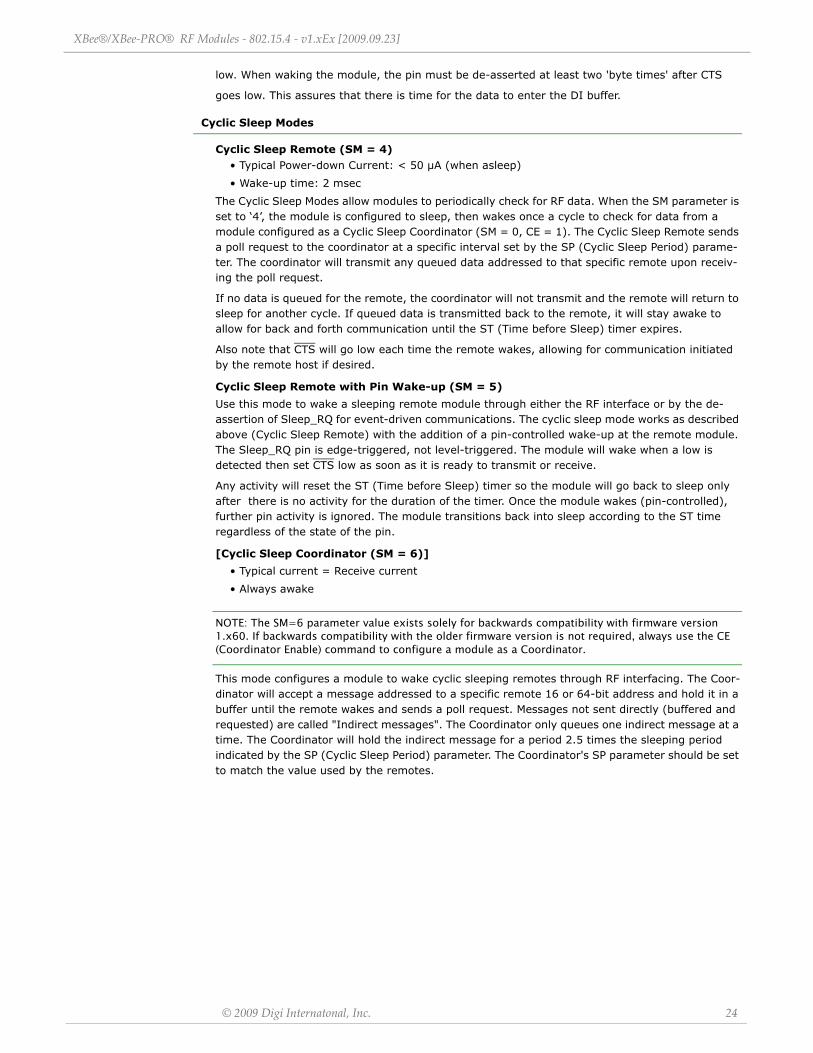
XBee®/XBee‐PRO® RF Modules ‐ 802.15.4 ‐ v1.xEx [2009.09.23]
© 2009 Digi Internatonal, Inc. 24
low. When waking the module, the pin must be de-asserted at least two 'byte times' after CTS
goes low. This assures that there is time for the data to enter the DI buffer.
Cyclic Sleep Modes
Cyclic Sleep Remote (SM = 4)• Typical Power-down Current: < 50 µA (when asleep)
• Wake-up time: 2 msec
The Cyclic Sleep Modes allow modules to periodically check for RF data. When the SM parameter is set to ‘4’, the module is configured to sleep, then wakes once a cycle to check for data from a module configured as a Cyclic Sleep Coordinator (SM = 0, CE = 1). The Cyclic Sleep Remote sends a poll request to the coordinator at a specific interval set by the SP (Cyclic Sleep Period) parame-ter. The coordinator will transmit any queued data addressed to that specific remote upon receiv-ing the poll request.
If no data is queued for the remote, the coordinator will not transmit and the remote will return to sleep for another cycle. If queued data is transmitted back to the remote, it will stay awake to allow for back and forth communication until the ST (Time before Sleep) timer expires.
Also note that CTS will go low each time the remote wakes, allowing for communication initiated by the remote host if desired.
Cyclic Sleep Remote with Pin Wake-up (SM = 5)
Use this mode to wake a sleeping remote module through either the RF interface or by the de-assertion of Sleep_RQ for event-driven communications. The cyclic sleep mode works as described above (Cyclic Sleep Remote) with the addition of a pin-controlled wake-up at the remote module. The Sleep_RQ pin is edge-triggered, not level-triggered. The module will wake when a low is detected then set CTS low as soon as it is ready to transmit or receive.
Any activity will reset the ST (Time before Sleep) timer so the module will go back to sleep only after there is no activity for the duration of the timer. Once the module wakes (pin-controlled), further pin activity is ignored. The module transitions back into sleep according to the ST time regardless of the state of the pin.
[Cyclic Sleep Coordinator (SM = 6)]
• Typical current = Receive current
• Always awake
NOTE: The SM=6 parameter value exists solely for backwards compatibility with firmware version 1.x60. If backwards compatibility with the older firmware version is not required, always use the CE (Coordinator Enable) command to configure a module as a Coordinator.
This mode configures a module to wake cyclic sleeping remotes through RF interfacing. The Coor-dinator will accept a message addressed to a specific remote 16 or 64-bit address and hold it in a buffer until the remote wakes and sends a poll request. Messages not sent directly (buffered and requested) are called "Indirect messages". The Coordinator only queues one indirect message at a time. The Coordinator will hold the indirect message for a period 2.5 times the sleeping period indicated by the SP (Cyclic Sleep Period) parameter. The Coordinator's SP parameter should be set to match the value used by the remotes.
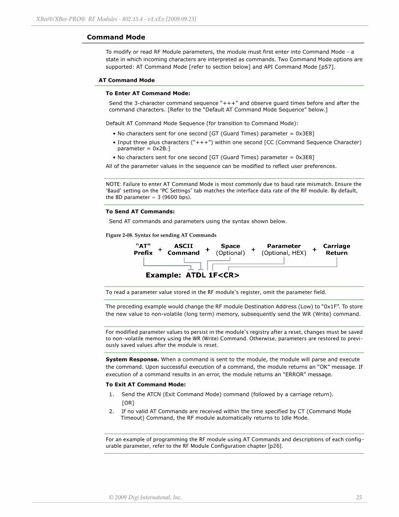
XBee®/XBee‐PRO® RF Modules ‐ 802.15.4 ‐ v1.xEx [2009.09.23]
© 2009 Digi Internatonal, Inc. 25
Command Mode
To modify or read RF Module parameters, the module must first enter into Command Mode - a state in which incoming characters are interpreted as commands. Two Command Mode options are supported: AT Command Mode [refer to section below] and API Command Mode [p57].
AT Command Mode
To Enter AT Command Mode:
Default AT Command Mode Sequence (for transition to Command Mode):
• No characters sent for one second [GT (Guard Times) parameter = 0x3E8]
• Input three plus characters (“+++”) within one second [CC (Command Sequence Character) parameter = 0x2B.]
• No characters sent for one second [GT (Guard Times) parameter = 0x3E8]
All of the parameter values in the sequence can be modified to reflect user preferences.
NOTE: Failure to enter AT Command Mode is most commonly due to baud rate mismatch. Ensure the ‘Baud’ setting on the “PC Settings” tab matches the interface data rate of the RF module. By default, the BD parameter = 3 (9600 bps).
To Send AT Commands:
Figure 2‐08. Syntax for sending AT Commands
To read a parameter value stored in the RF module’s register, omit the parameter field.
The preceding example would change the RF module Destination Address (Low) to “0x1F”. To store the new value to non-volatile (long term) memory, subsequently send the WR (Write) command.
For modified parameter values to persist in the module’s registry after a reset, changes must be saved to non-volatile memory using the WR (Write) Command. Otherwise, parameters are restored to previ-ously saved values after the module is reset.
System Response. When a command is sent to the module, the module will parse and execute the command. Upon successful execution of a command, the module returns an “OK” message. If execution of a command results in an error, the module returns an “ERROR” message.
To Exit AT Command Mode:
For an example of programming the RF module using AT Commands and descriptions of each config-urable parameter, refer to the RF Module Configuration chapter [p26].
Send the 3-character command sequence “+++” and observe guard times before and after the command characters. [Refer to the “Default AT Command Mode Sequence” below.]
Send AT commands and parameters using the syntax shown below.
1. Send the ATCN (Exit Command Mode) command (followed by a carriage return).
[OR]
2. If no valid AT Commands are received within the time specified by CT (Command Mode Timeout) Command, the RF module automatically returns to Idle Mode.
© 2009 Digi International Inc. 26
3. RF Module Configuration
Programming the RF Module
Refer to the Command Mode section [p25] for more information about entering Command Mode, sending AT commands and exiting Command Mode. For information regarding module program-ming using API Mode, refer to the API Operation sections [p57].
Programming Examples
Setup
Sample Configuration: Modify RF Module Destination Address
Sample Configuration: Restore RF Module Defaults
The programming examples in this section require the installation of Digi's X-CTU Software and a serial connection to a PC. (Digi stocks RS-232 and USB boards to facilitate interfacing with a PC.)
1. Install Digi's X-CTU Software to a PC by double-clicking the "setup_X-CTU.exe" file. (The file is located on the Digi CD and www.digi.com/xctu.)
2. Mount the RF module to an interface board, then connect the module assembly to a PC.
3. Launch the X-CTU Software and select the 'PC Settings' tab. Verify the baud and parity set-tings of the Com Port match those of the RF module.
NOTE: Failure to enter AT Command Mode is most commonly due to baud rate mismatch. Ensure the ‘Baud’ setting on the ‘PC Settings’ tab matches the interface data rate of the RF mod-ule. By default, the BD parameter = 3 (which corresponds to 9600 bps).
Example: Utilize the X-CTU “Terminal” tab to change the RF module's DL (Destination Address Low) parameter and save the new address to non-volatile memory.
After establishing a serial connection between the RF module and a PC [refer to the 'Setup' sec-tion above], select the “Terminal” tab of the X-CTU Software and enter the following command lines (‘CR’ stands for carriage return):
Method 1 (One line per command)
Send AT Command +++ ATDL <Enter> ATDL1A0D <Enter> ATWR <Enter> ATCN <Enter>
System Response OK <CR> (Enter into Command Mode) current value <CR> (Read Destination Address Low) OK <CR> (Modify Destination Address Low) OK <CR> (Write to non-volatile memory) OK <CR> (Exit Command Mode)
Method 2 (Multiple commands on one line)
Send AT Command +++ ATDL <Enter> ATDL1A0D,WR,CN <Enter>
System Response OK <CR> (Enter into Command Mode) current value <CR> (Read Destination Address Low) OK<CR> OK<CR> OK<CR>
Example: Utilize the X-CTU “Modem Configuration” tab to restore default parameter values.
After establishing a connection between the module and a PC [refer to the 'Setup' section above], select the “Modem Configuration” tab of the X-CTU Software.
1. Select the 'Read' button.
2. Select the 'Restore' button.
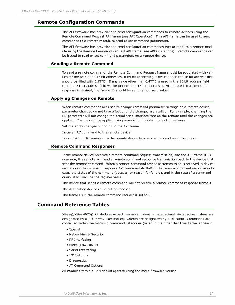
XBee®/XBee‐PRO® RF Modules ‐ 802.15.4 ‐ v1.xEx [2009.09.23]
© 2009 Digi Internatonal, Inc. 27
Remote Configuration Commands
The API firmware has provisions to send configuration commands to remote devices using the Remote Command Request API frame (see API Operation). This API frame can be used to send commands to a remote module to read or set command parameters.
The API firmware has provisions to send configuration commands (set or read) to a remote mod-ule using the Remote Command Request API frame (see API Operations). Remote commands can be issued to read or set command parameters on a remote device.
Sending a Remote Command
To send a remote command, the Remote Command Request frame should be populated with val-ues for the 64 bit and 16 bit addresses. If 64 bit addressing is desired then the 16 bit address field should be filled with 0xFFFE. If any value other than 0xFFFE is used in the 16 bit address field then the 64 bit address field will be ignored and 16 bit addressing will be used. If a command response is desired, the Frame ID should be set to a non-zero value.
Applying Changes on Remote
When remote commands are used to change command parameter settings on a remote device, parameter changes do not take effect until the changes are applied. For example, changing the BD parameter will not change the actual serial interface rate on the remote until the changes are applied. Changes can be applied using remote commands in one of three ways:
Set the apply changes option bit in the API frame
Issue an AC command to the remote device
Issue a WR + FR command to the remote device to save changes and reset the device.
Remote Command Responses
If the remote device receives a remote command request transmission, and the API frame ID is non-zero, the remote will send a remote command response transmission back to the device that sent the remote command. When a remote command response transmission is received, a device sends a remote command response API frame out its UART. The remote command response indi-cates the status of the command (success, or reason for failure), and in the case of a command query, it will include the register value.
The device that sends a remote command will not receive a remote command response frame if:
The destination device could not be reached
The frame ID in the remote command request is set to 0.
Command Reference Tables
XBee®/XBee-PRO® RF Modules expect numerical values in hexadecimal. Hexadecimal values are designated by a “0x” prefix. Decimal equivalents are designated by a “d” suffix. Commands are contained within the following command categories (listed in the order that their tables appear):
• Special
• Networking & Security
• RF Interfacing
• Sleep (Low Power)
• Serial Interfacing
• I/O Settings
• Diagnostics
• AT Command Options
All modules within a PAN should operate using the same firmware version.
XBee®/XBee‐PRO® RF Modules ‐ 802.15.4 ‐ v1.xEx [2009.09.23]
© 2009 Digi Internatonal, Inc. 28
Special
* Firmware version in which the command was first introduced (firmware versions are numbered in hexadecimal notation.)
Networking & Security
Table 3‐01. XBee‐PRO Commands ‐ SpecialAT Command
Command Category Name and Description Parameter Range Default
WR SpecialWrite. Write parameter values to non-volatile memory so that parameter modifications persist through subsequent power-up or reset. Note: Once WR is issued, no additional characters should be sent to the module until after the response "OK\r" is received.
- -
RE Special Restore Defaults. Restore module parameters to factory defaults. - -
FR ( v1.x80*) Special Software Reset. Responds immediately with an OK then performs a hard reset ~100ms later. - -
Table 3‐02. XBee®/XBee‐PRO® Commands ‐ Networking & Security (Sub‐categories designated within brackets)AT Command
Command Category Name and Description Parameter Range Default
CH Networking Addressing
Channel. Set/Read the channel number used for transmitting and receiving data between RF modules (uses 802.15.4 protocol channel numbers).
0x0B - 0x1A (XBee) 0x0C - 0x17 (XBee-PRO) 0x0C (12d)
ID Networking Addressing
PAN ID. Set/Read the PAN (Personal Area Network) ID. Use 0xFFFF to broadcast messages to all PANs. 0 - 0xFFFF 0x3332
(13106d)
DH Networking Addressing
Destination Address High. Set/Read the upper 32 bits of the 64-bit destination address. When combined with DL, it defines the destination address used for transmission. To transmit using a 16-bit address, set DH parameter to zero and DL less than 0xFFFF. 0x000000000000FFFF is the broadcast address for the PAN.
0 - 0xFFFFFFFF 0
DL Networking Addressing
Destination Address Low. Set/Read the lower 32 bits of the 64-bit destination address. When combined with DH, DL defines the destination address used for transmission. To transmit using a 16-bit address, set DH parameter to zero and DL less than 0xFFFF. 0x000000000000FFFF is the broadcast address for the PAN.
0 - 0xFFFFFFFF 0
MY Networking Addressing
16-bit Source Address. Set/Read the RF module 16-bit source address. Set MY = 0xFFFF to disable reception of packets with 16-bit addresses. 64-bit source address (serial number) and broadcast address (0x000000000000FFFF) is always enabled.
0 - 0xFFFF 0
SH Networking Addressing
Serial Number High. Read high 32 bits of the RF module's unique IEEE 64-bit address. 64-bit source address is always enabled. 0 - 0xFFFFFFFF [read-only] Factory-set
SL Networking Addressing
Serial Number Low. Read low 32 bits of the RF module's unique IEEE 64-bit address. 64-bit source address is always enabled. 0 - 0xFFFFFFFF [read-only] Factory-set
RR ( v1.xA0*) Networking Addressing
XBee Retries. Set/Read the maximum number of retries the module will execute in addition to the 3 retries provided by the 802.15.4 MAC. For each XBee retry, the 802.15.4 MAC can execute up to 3 retries.
0 - 6 0
RN Networking Addressing
Random Delay Slots. Set/Read the minimum value of the back-off exponent in the CSMA-CA algorithm that is used for collision avoidance. If RN = 0, collision avoidance is disabled during the first iteration of the algorithm (802.15.4 - macMinBE).
0 - 3 [exponent] 0
MM ( v1.x80*) Networking Addressing
MAC Mode. MAC Mode. Set/Read MAC Mode value. MAC Mode enables/disables the use of a Digi header in the 802.15.4 RF packet. When Modes 0 or 3 are enabled (MM=0,3), duplicate packet detection is enabled as well as certain AT commands. Please see the detailed MM description on page 47 for additional information.
0 - 30 = Digi Mode1 = 802.15.4 (no ACKs)2 = 802.15.4 (with ACKs)3 = Digi Mode (no ACKs)
0
NI ( v1.x80*) Networking Identification
Node Identifier. Stores a string identifier. The register only accepts printable ASCII data. A string can not start with a space. Carriage return ends command. Command will automatically end when maximum bytes for the string have been entered. This string is returned as part of the ND (Node Discover) command. This identifier is also used with the DN (Destination Node) command.
20-character ASCII string -
ND ( v1.x80*) Networking Identification
Node Discover. Discovers and reports all RF modules found. The following information is reported for each module discovered (the example cites use of Transparent operation (AT command format) - refer to the long ND command description regarding differences between Transparent and API operation).
MY<CR> SH<CR> SL<CR> DB<CR> NI<CR><CR>
The amount of time the module allows for responses is determined by the NT parameter. In Transparent operation, command completion is designated by a <CR> (carriage return). ND also accepts a Node Identifier as a parameter. In this case, only a module matching the supplied identifier will respond. If ND self-response is enabled (NO=1) the module initiating the node discover will also output a response for itself.
optional 20-character NI value
NT ( v1.xA0*) Networking Identification
Node Discover Time. Set/Read the amount of time a node will wait for responses from other nodes when using the ND (Node Discover) command. 0x01 - 0xFC [x 100 ms] 0x19
XBee®/XBee‐PRO® RF Modules ‐ 802.15.4 ‐ v1.xEx [2009.09.23]
© 2009 Digi Internatonal, Inc. 29
NO (v1xC5) Networking Identification Node Discover Options. Enables node discover self-response on the module. 0-1 0
DN ( v1.x80*) Networking Identification
Destination Node. Resolves an NI (Node Identifier) string to a physical address. The following events occur upon successful command execution:
1. DL and DH are set to the address of the module with the matching Node Identifier. 2. “OK” is returned. 3. RF module automatically exits AT Command Mode
If there is no response from a module within 200 msec or a parameter is not specified (left blank), the command is terminated and an “ERROR” message is returned.
20-character ASCII string -
CE ( v1.x80*) Networking Association Coordinator Enable. Set/Read the coordinator setting.
0 - 10 = End Device 1 = Coordinator
0
SC ( v1.x80*) Networking Association
Scan Channels. Set/Read list of channels to scan for all Active and Energy Scans as a bitfield. This affects scans initiated in command mode (AS, ED) and during End Device Association and Coordinator startup:
bit 0 - 0x0B bit 4 - 0x0F bit 8 - 0x13 bit12 - 0x17 bit 1 - 0x0C bit 5 - 0x10 bit 9 - 0x14 bit13 - 0x18 bit 2 - 0x0D bit 6 - 0x11 bit 10 - 0x15 bit14 - 0x19 bit 3 - 0x0E bit 7 - 0x12 bit 11 - 0x16 bit 15 - 0x1A
0 - 0xFFFF [bitfield] (bits 0, 14, 15 not allowed on the XBee-PRO)
0x1FFE(all XBee-PRO Channels)
SD ( v1.x80*) Networking Association
Scan Duration. Set/Read the scan duration exponent. End Device - Duration of Active Scan during Association. Coordinator - If ‘ReassignPANID’ option is set on Coordinator [refer to A2 parameter], SD determines the length of time the Coordinator will scan channels to locate existing PANs. If ‘ReassignChannel’ option is set, SD determines how long the Coordinator will perform an Energy Scan to determine which channel it will operate on.‘Scan Time’ is measured as (# of channels to scan] * (2 ^ SD) * 15.36ms). The number of channels to scan is set by the SC command. The XBee can scan up to 16 channels (SC = 0xFFFF). The XBee PRO can scan up to 13 channels (SC = 0x3FFE).Example: The values below show results for a 13 channel scan:
If SD = 0, time = 0.18 sec SD = 8, time = 47.19 sec SD = 2, time = 0.74 sec SD = 10, time = 3.15 min SD = 4, time = 2.95 sec SD = 12, time = 12.58 min SD = 6, time = 11.80 sec SD = 14, time = 50.33 min
0-0x0F [exponent] 4
A1 ( v1.x80*) Networking Association
End Device Association. Set/Read End Device association options. bit 0 - ReassignPanID
0 - Will only associate with Coordinator operating on PAN ID that matches module ID 1 - May associate with Coordinator operating on any PAN ID
bit 1 - ReassignChannel 0 - Will only associate with Coordinator operating on matching CH Channel setting 1 - May associate with Coordinator operating on any Channel
bit 2 - AutoAssociate 0 - Device will not attempt Association 1 - Device attempts Association until success
Note: This bit is used only for Non-Beacon systems. End Devices in Beacon-enabled system must always associate to a Coordinatorbit 3 - PollCoordOnPinWake
0 - Pin Wake will not poll the Coordinator for indirect (pending) data 1 - Pin Wake will send Poll Request to Coordinator to extract any pending data
bits 4 - 7 are reserved
0 - 0x0F [bitfield] 0
A2 ( v1.x80*) Networking Association
Coordinator Association. Set/Read Coordinator association options. bit 0 - ReassignPanID
0 - Coordinator will not perform Active Scan to locate available PAN ID. It will operate on ID (PAN ID). 1 - Coordinator will perform Active Scan to determine an available ID (PAN ID). If a
PAN ID conflict is found, the ID parameter will change. bit 1 - ReassignChannel -
0 - Coordinator will not perform Energy Scan to determine free channel. It will operate on the channel determined by the CH parameter. 1 - Coordinator will perform Energy Scan to find a free channel, then operate on that channel.
bit 2 - AllowAssociation - 0 - Coordinator will not allow any devices to associate to it. 1 - Coordinator will allow devices to associate to it.
bits 3 - 7 are reserved
0 - 7 [bitfield] 0
Table 3‐02. XBee®/XBee‐PRO® Commands ‐ Networking & Security (Sub‐categories designated within brackets)AT Command
Command Category Name and Description Parameter Range Default
XBee®/XBee‐PRO® RF Modules ‐ 802.15.4 ‐ v1.xEx [2009.09.23]
© 2009 Digi Internatonal, Inc. 30
* Firmware version in which the command was first introduced (firmware versions are numbered in hexadecimal notation.)
AI ( v1.x80*) Networking Association
Association Indication. Read errors with the last association request:0x00 - Successful Completion - Coordinator successfully started or End Device
association complete 0x01 - Active Scan Timeout 0x02 - Active Scan found no PANs 0x03 - Active Scan found PAN, but the CoordinatorAllowAssociation bit is not set 0x04 - Active Scan found PAN, but Coordinator and End Device are not
configured to support beacons 0x05 - Active Scan found PAN, but the Coordinator ID parameter does not match
the ID parameter of the End Device 0x06 - Active Scan found PAN, but the Coordinator CH parameter does not match the
CH parameter of the End Device 0x07 - Energy Scan Timeout 0x08 - Coordinator start request failed 0x09 - Coordinator could not start due to invalid parameter 0x0A - Coordinator Realignment is in progress 0x0B - Association Request not sent 0x0C - Association Request timed out - no reply was received 0x0D - Association Request had an Invalid Parameter 0x0E - Association Request Channel Access Failure. Request was not transmitted -
CCA failure 0x0F - Remote Coordinator did not send an ACK after Association Request was sent 0x10 - Remote Coordinator did not reply to the Association Request, but an ACK was
received after sending the request 0x11 - [reserved] 0x12 - Sync-Loss - Lost synchronization with a Beaconing Coordinator 0x13 - Disassociated - No longer associated to Coordinator0xFF - RF Module is attempting to associate
0 - 0x13 [read-only] -
DA ( v1.x80*) Networking Association
Force Disassociation. End Device will immediately disassociate from a Coordinator (if associated) and reattempt to associate. - -
FP ( v1.x80*) Networking Association Force Poll. Request indirect messages being held by a coordinator. - -
AS ( v1.x80*) Networking Association
Active Scan. Send Beacon Request to Broadcast Address (0xFFFF) and Broadcast PAN (0xFFFF) on every channel. The parameter determines the time the radio will listen for Beacons on each channel. A PanDescriptor is created and returned for every Beacon received from the scan. Each PanDescriptor contains the following information:CoordAddress (SH, SL)<CR> CoordPanID (ID)<CR> CoordAddrMode <CR>
0x02 = 16-bit Short Address 0x03 = 64-bit Long Address
Channel (CH parameter) <CR> SecurityUse<CR> ACLEntry<CR> SecurityFailure<CR> SuperFrameSpec<CR> (2 bytes):
bit 15 - Association Permitted (MSB) bit 14 - PAN Coordinator bit 13 - Reserved bit 12 - Battery Life Extension bits 8-11 - Final CAP Slot bits 4-7 - Superframe Order bits 0-3 - Beacon Order
GtsPermit<CR> RSSI<CR> (RSSI is returned as -dBm) TimeStamp<CR> (3 bytes) <CR> A carriage return <CR> is sent at the end of the AS command. The Active Scan is capable of returning up to 5 PanDescriptors in a scan. The actual scan time on each channel is measured as Time = [(2 ^SD PARAM) * 15.36] ms. Note the total scan time is this time multiplied by the number of channels to be scanned (16 for the XBee and 13 for the XBee-PRO). Also refer to SD command description.
0 - 6 -
ED ( v1.x80*) Networking Association
Energy Scan. Send an Energy Detect Scan. This parameter determines the length of scan on each channel. The maximal energy on each channel is returned & each value is followed by a carriage return. An additional carriage return is sent at the end of the command. The values returned represent the detected energy level in units of -dBm. The actual scan time on each channel is measured as Time = [(2 ^ED) * 15.36] ms. Note the total scan time is this time multiplied by the number of channels to be scanned (refer to SD parameter).
0 - 6 -
EE ( v1.xA0*) Networking Security
AES Encryption Enable. Disable/Enable 128-bit AES encryption support. Use in conjunction with the KY command. 0 - 1 0 (disabled)
KY ( v1.xA0*) Networking Security
AES Encryption Key. Set the 128-bit AES (Advanced Encryption Standard) key for encrypting/decrypting data. The KY register cannot be read. 0 - (any 16-Byte value) -
Table 3‐02. XBee®/XBee‐PRO® Commands ‐ Networking & Security (Sub‐categories designated within brackets)AT Command
Command Category Name and Description Parameter Range Default
XBee®/XBee‐PRO® RF Modules ‐ 802.15.4 ‐ v1.xEx [2009.09.23]
© 2009 Digi Internatonal, Inc. 31
RF Interfacing
* Firmware version in which the command was first introduced (firmware versions are numbered in hexadecimal notation.)Sleep (Low Power)
Table 3‐03. XBee/XBee‐PRO Commands ‐ RF InterfacingAT Command
Command Category Name and Description Parameter Range Default
PL RF Interfacing Power Level. Select/Read the power level at which the RF module transmits conducted power.
0 - 4 (XBee / XBee-PRO) 0 = -10 / 10 dBm 1 = -6 / 12 dBm 2 = -4 / 14 dBm 3 = -2 / 16 dBm 4 = 0 / 18 dBm
XBee-PRO International variant: PL=4: 10 dBm PL=3: 8 dBm PL=2: 2 dBm PL=1: -3 dBm PL=0: -3 dBm
4
CA (v1.x80*) RF InterfacingCCA Threshold. Set/read the CCA (Clear Channel Assessment) threshold. Prior to transmitting a packet, a CCA is performed to detect energy on the channel. If the detected energy is above the CCA Threshold, the module will not transmit the packet.
0x24 - 0x50 [-dBm] 0x2C(-44d dBm)
Table 3‐04. XBee®/XBee‐PRO® Commands ‐ Sleep (Low Power)AT Command
Command Category Name and Description Parameter Range Default
SM Sleep (Low Power) Sleep Mode. Set/Read Sleep Mode configurations.
0 - 5 0 = No Sleep 1 = Pin Hibernate 2 = Pin Doze 3 = Reserved 4 = Cyclic sleep remote 5 = Cyclic sleep remote w/ pin wake-up6 = [Sleep Coordinator] for
backwards compatibility w/ v1.x6 only; otherwise, use CE command.
0
SO Sleep (Low Power)
Sleep Options Set/Read the sleep mode options. Bit 0 - Poll wakeup disable0 - Normal operations. A module configured for cyclic sleep will poll for data on waking.1 - Disable wakeup poll. A module configured for cyclic sleep will not poll for data on waking.Bit 1 - ADC/DIO wakeup sampling disable.0 - Normal operations. A module configured in a sleep mode with ADC/DIO sampling enabled will automatically perform a sampling on wakeup.1 - Suppress sample on wakeup. A module configured in a sleep mode with ADC/DIO sampling enabled will not automatically sample on wakeup.
0-4 0
ST Sleep (Low Power)
Time before Sleep. <NonBeacon firmware> Set/Read time period of inactivity (no serial or RF data is sent or received) before activating Sleep Mode. ST parameter is only valid with Cyclic Sleep settings (SM = 4 - 5).Coordinator and End Device ST values must be equal. Also note, the GT parameter value must always be less than the ST value. (If GT > ST, the configuration will render the module unable to enter into command mode.) If the ST parameter is modified, also modify the GT parameter accordingly.
1 - 0xFFFF [x 1 ms] 0x1388 (5000d)
SP Sleep (Low Power)
Cyclic Sleep Period. <NonBeacon firmware> Set/Read sleep period for cyclic sleeping remotes. Coordinator and End Device SP values should always be equal. To send Direct Messages, set SP = 0.End Device - SP determines the sleep period for cyclic sleeping remotes. Maximum sleep period is 268 seconds (0x68B0).Coordinator - If non-zero, SP determines the time to hold an indirect message before discarding it. A Coordinator will discard indirect messages after a period of (2.5 * SP).
0 - 0x68B0 [x 10 ms] 0
DP (1.x80*) Sleep (Low Power)
Disassociated Cyclic Sleep Period. <NonBeacon firmware> End Device - Set/Read time period of sleep for cyclic sleeping remotes that are configured for Association but are not associated to a Coordinator. (i.e. If a device is configured to associate, configured as a Cyclic Sleep remote, but does not find a Coordinator, it will sleep for DP time before reattempting association.) Maximum sleep period is 268 seconds (0x68B0). DP should be > 0 for NonBeacon systems.
1 - 0x68B0 [x 10 ms] 0x3E8 (1000d)
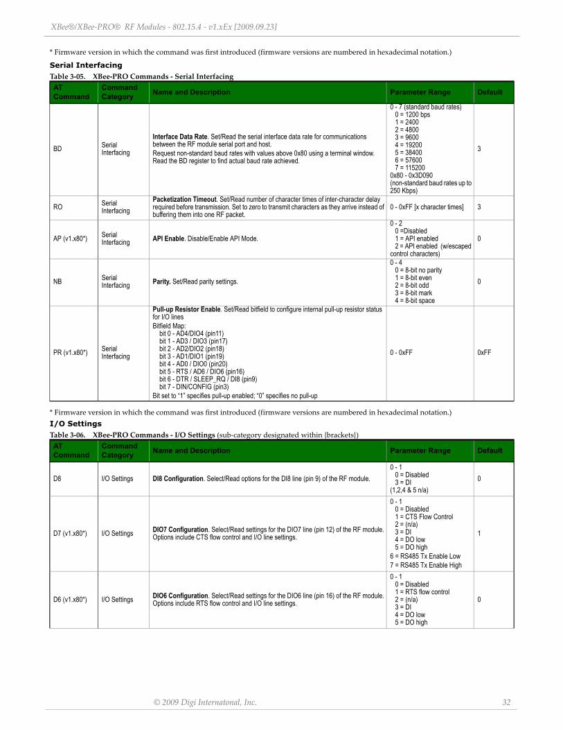
XBee®/XBee‐PRO® RF Modules ‐ 802.15.4 ‐ v1.xEx [2009.09.23]
© 2009 Digi Internatonal, Inc. 32
* Firmware version in which the command was first introduced (firmware versions are numbered in hexadecimal notation.)
Serial Interfacing
* Firmware version in which the command was first introduced (firmware versions are numbered in hexadecimal notation.)I/O Settings
Table 3‐05. XBee‐PRO Commands ‐ Serial InterfacingAT Command
Command Category Name and Description Parameter Range Default
BD Serial Interfacing
Interface Data Rate. Set/Read the serial interface data rate for communications between the RF module serial port and host. Request non-standard baud rates with values above 0x80 using a terminal window. Read the BD register to find actual baud rate achieved.
0 - 7 (standard baud rates) 0 = 1200 bps 1 = 2400 2 = 4800 3 = 9600 4 = 19200 5 = 38400 6 = 57600 7 = 115200
0x80 - 0x3D090 (non-standard baud rates up to 250 Kbps)
3
RO Serial Interfacing
Packetization Timeout. Set/Read number of character times of inter-character delay required before transmission. Set to zero to transmit characters as they arrive instead of buffering them into one RF packet.
0 - 0xFF [x character times] 3
AP (v1.x80*) Serial Interfacing API Enable. Disable/Enable API Mode.
0 - 2 0 =Disabled 1 = API enabled 2 = API enabled (w/escaped
control characters)
0
NB Serial Interfacing Parity. Set/Read parity settings.
0 - 4 0 = 8-bit no parity 1 = 8-bit even 2 = 8-bit odd 3 = 8-bit mark 4 = 8-bit space
0
PR (v1.x80*) Serial Interfacing
Pull-up Resistor Enable. Set/Read bitfield to configure internal pull-up resistor status for I/O lines Bitfield Map:
bit 0 - AD4/DIO4 (pin11) bit 1 - AD3 / DIO3 (pin17) bit 2 - AD2/DIO2 (pin18) bit 3 - AD1/DIO1 (pin19) bit 4 - AD0 / DIO0 (pin20) bit 5 - RTS / AD6 / DIO6 (pin16) bit 6 - DTR / SLEEP_RQ / DI8 (pin9) bit 7 - DIN/CONFIG (pin3)
Bit set to “1” specifies pull-up enabled; “0” specifies no pull-up
0 - 0xFF 0xFF
Table 3‐06. XBee‐PRO Commands ‐ I/O Settings (sub‐category designated within brackets)AT Command
Command Category Name and Description Parameter Range Default
D8 I/O Settings DI8 Configuration. Select/Read options for the DI8 line (pin 9) of the RF module.0 - 1
0 = Disabled 3 = DI
(1,2,4 & 5 n/a)0
D7 (v1.x80*) I/O Settings DIO7 Configuration. Select/Read settings for the DIO7 line (pin 12) of the RF module. Options include CTS flow control and I/O line settings.
0 - 1 0 = Disabled 1 = CTS Flow Control 2 = (n/a) 3 = DI 4 = DO low 5 = DO high
6 = RS485 Tx Enable Low7 = RS485 Tx Enable High
1
D6 (v1.x80*) I/O Settings DIO6 Configuration. Select/Read settings for the DIO6 line (pin 16) of the RF module. Options include RTS flow control and I/O line settings.
0 - 1 0 = Disabled 1 = RTS flow control 2 = (n/a) 3 = DI 4 = DO low 5 = DO high
0
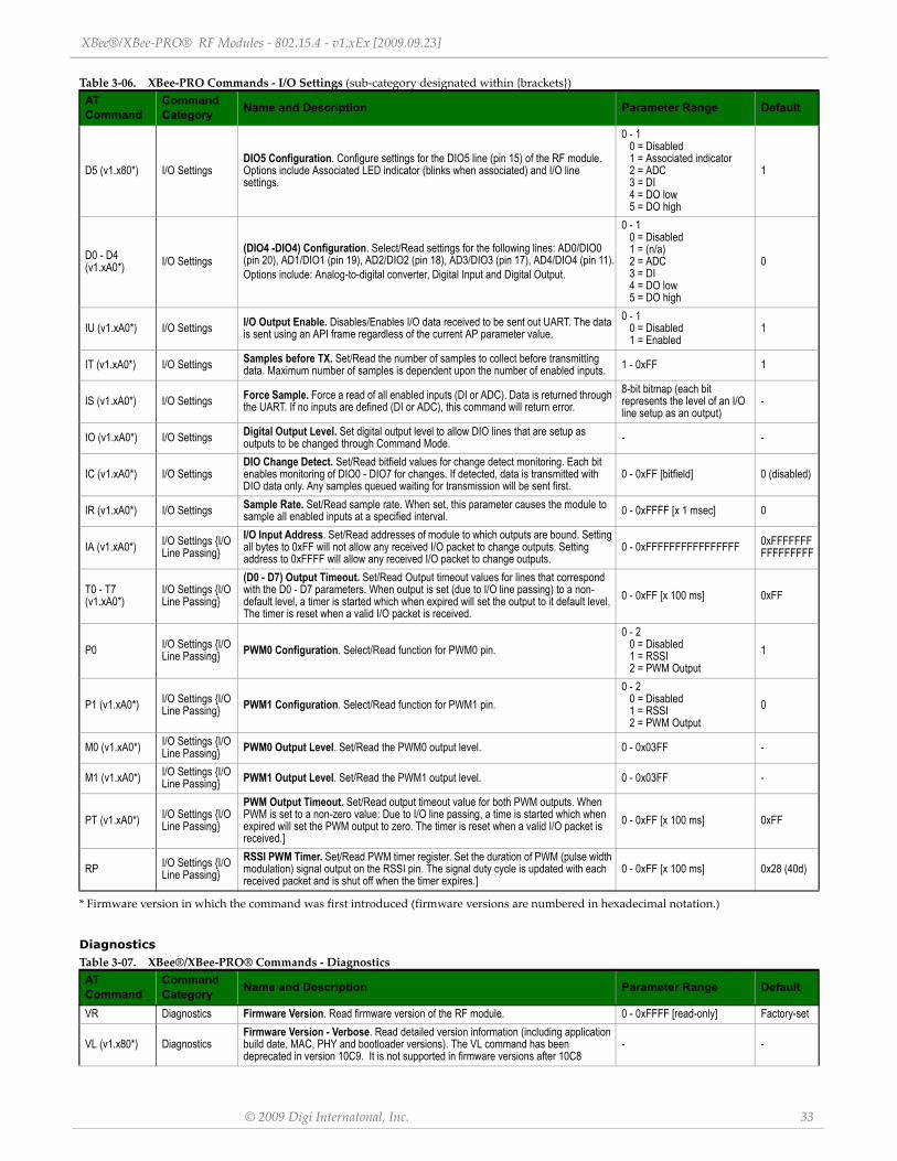
XBee®/XBee‐PRO® RF Modules ‐ 802.15.4 ‐ v1.xEx [2009.09.23]
© 2009 Digi Internatonal, Inc. 33
* Firmware version in which the command was first introduced (firmware versions are numbered in hexadecimal notation.)
Diagnostics
D5 (v1.x80*) I/O SettingsDIO5 Configuration. Configure settings for the DIO5 line (pin 15) of the RF module. Options include Associated LED indicator (blinks when associated) and I/O line settings.
0 - 1 0 = Disabled 1 = Associated indicator 2 = ADC 3 = DI 4 = DO low 5 = DO high
1
D0 - D4 (v1.xA0*) I/O Settings
(DIO4 -DIO4) Configuration. Select/Read settings for the following lines: AD0/DIO0 (pin 20), AD1/DIO1 (pin 19), AD2/DIO2 (pin 18), AD3/DIO3 (pin 17), AD4/DIO4 (pin 11).Options include: Analog-to-digital converter, Digital Input and Digital Output.
0 - 1 0 = Disabled 1 = (n/a) 2 = ADC 3 = DI 4 = DO low 5 = DO high
0
IU (v1.xA0*) I/O Settings I/O Output Enable. Disables/Enables I/O data received to be sent out UART. The data is sent using an API frame regardless of the current AP parameter value.
0 - 1 0 = Disabled 1 = Enabled
1
IT (v1.xA0*) I/O Settings Samples before TX. Set/Read the number of samples to collect before transmitting data. Maximum number of samples is dependent upon the number of enabled inputs. 1 - 0xFF 1
IS (v1.xA0*) I/O Settings Force Sample. Force a read of all enabled inputs (DI or ADC). Data is returned through the UART. If no inputs are defined (DI or ADC), this command will return error.
8-bit bitmap (each bit represents the level of an I/O line setup as an output)
-
IO (v1.xA0*) I/O Settings Digital Output Level. Set digital output level to allow DIO lines that are setup as outputs to be changed through Command Mode. - -
IC (v1.xA0*) I/O SettingsDIO Change Detect. Set/Read bitfield values for change detect monitoring. Each bit enables monitoring of DIO0 - DIO7 for changes. If detected, data is transmitted with DIO data only. Any samples queued waiting for transmission will be sent first.
0 - 0xFF [bitfield] 0 (disabled)
IR (v1.xA0*) I/O Settings Sample Rate. Set/Read sample rate. When set, this parameter causes the module to sample all enabled inputs at a specified interval. 0 - 0xFFFF [x 1 msec] 0
IA (v1.xA0*) I/O Settings I/O Line Passing
I/O Input Address. Set/Read addresses of module to which outputs are bound. Setting all bytes to 0xFF will not allow any received I/O packet to change outputs. Setting address to 0xFFFF will allow any received I/O packet to change outputs.
0 - 0xFFFFFFFFFFFFFFFF 0xFFFFFFFFFFFFFFFF
T0 - T7 (v1.xA0*)
I/O Settings I/O Line Passing
(D0 - D7) Output Timeout. Set/Read Output timeout values for lines that correspond with the D0 - D7 parameters. When output is set (due to I/O line passing) to a non-default level, a timer is started which when expired will set the output to it default level. The timer is reset when a valid I/O packet is received.
0 - 0xFF [x 100 ms] 0xFF
P0 I/O Settings I/O Line Passing PWM0 Configuration. Select/Read function for PWM0 pin.
0 - 2 0 = Disabled 1 = RSSI 2 = PWM Output
1
P1 (v1.xA0*) I/O Settings I/O Line Passing PWM1 Configuration. Select/Read function for PWM1 pin.
0 - 2 0 = Disabled 1 = RSSI 2 = PWM Output
0
M0 (v1.xA0*) I/O Settings I/O Line Passing PWM0 Output Level. Set/Read the PWM0 output level. 0 - 0x03FF -
M1 (v1.xA0*) I/O Settings I/O Line Passing PWM1 Output Level. Set/Read the PWM1 output level. 0 - 0x03FF -
PT (v1.xA0*) I/O Settings I/O Line Passing
PWM Output Timeout. Set/Read output timeout value for both PWM outputs. When PWM is set to a non-zero value: Due to I/O line passing, a time is started which when expired will set the PWM output to zero. The timer is reset when a valid I/O packet is received.]
0 - 0xFF [x 100 ms] 0xFF
RP I/O Settings I/O Line Passing
RSSI PWM Timer. Set/Read PWM timer register. Set the duration of PWM (pulse width modulation) signal output on the RSSI pin. The signal duty cycle is updated with each received packet and is shut off when the timer expires.]
0 - 0xFF [x 100 ms] 0x28 (40d)
Table 3‐07. XBee®/XBee‐PRO® Commands ‐ DiagnosticsAT Command
Command Category Name and Description Parameter Range Default
VR Diagnostics Firmware Version. Read firmware version of the RF module. 0 - 0xFFFF [read-only] Factory-set
VL (v1.x80*) DiagnosticsFirmware Version - Verbose. Read detailed version information (including application build date, MAC, PHY and bootloader versions). The VL command has been deprecated in version 10C9. It is not supported in firmware versions after 10C8
- -
Table 3‐06. XBee‐PRO Commands ‐ I/O Settings (sub‐category designated within brackets)AT Command
Command Category Name and Description Parameter Range Default
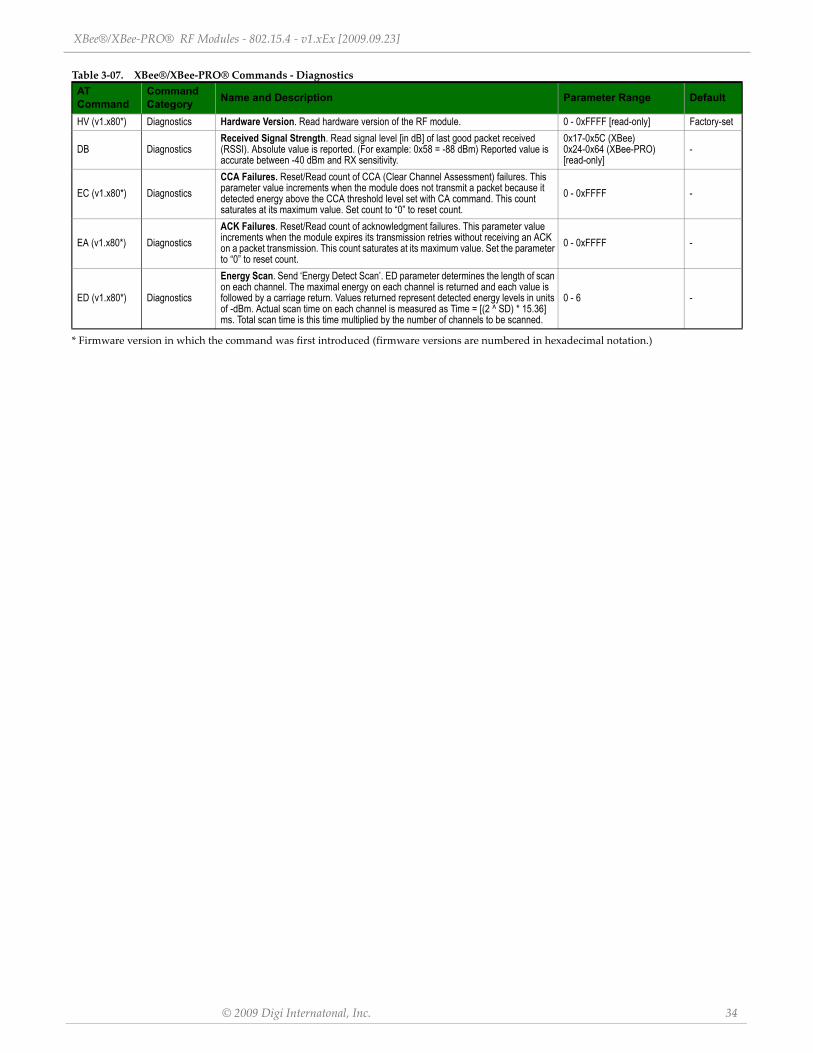
XBee®/XBee‐PRO® RF Modules ‐ 802.15.4 ‐ v1.xEx [2009.09.23]
© 2009 Digi Internatonal, Inc. 34
* Firmware version in which the command was first introduced (firmware versions are numbered in hexadecimal notation.)
HV (v1.x80*) Diagnostics Hardware Version. Read hardware version of the RF module. 0 - 0xFFFF [read-only] Factory-set
DB DiagnosticsReceived Signal Strength. Read signal level [in dB] of last good packet received (RSSI). Absolute value is reported. (For example: 0x58 = -88 dBm) Reported value is accurate between -40 dBm and RX sensitivity.
0x17-0x5C (XBee) 0x24-0x64 (XBee-PRO) [read-only]
-
EC (v1.x80*) DiagnosticsCCA Failures. Reset/Read count of CCA (Clear Channel Assessment) failures. This parameter value increments when the module does not transmit a packet because it detected energy above the CCA threshold level set with CA command. This count saturates at its maximum value. Set count to “0” to reset count.
0 - 0xFFFF -
EA (v1.x80*) DiagnosticsACK Failures. Reset/Read count of acknowledgment failures. This parameter value increments when the module expires its transmission retries without receiving an ACK on a packet transmission. This count saturates at its maximum value. Set the parameter to “0” to reset count.
0 - 0xFFFF -
ED (v1.x80*) Diagnostics
Energy Scan. Send ‘Energy Detect Scan’. ED parameter determines the length of scan on each channel. The maximal energy on each channel is returned and each value is followed by a carriage return. Values returned represent detected energy levels in units of -dBm. Actual scan time on each channel is measured as Time = [(2 ^ SD) * 15.36] ms. Total scan time is this time multiplied by the number of channels to be scanned.
0 - 6 -
Table 3‐07. XBee®/XBee‐PRO® Commands ‐ DiagnosticsAT Command
Command Category Name and Description Parameter Range Default
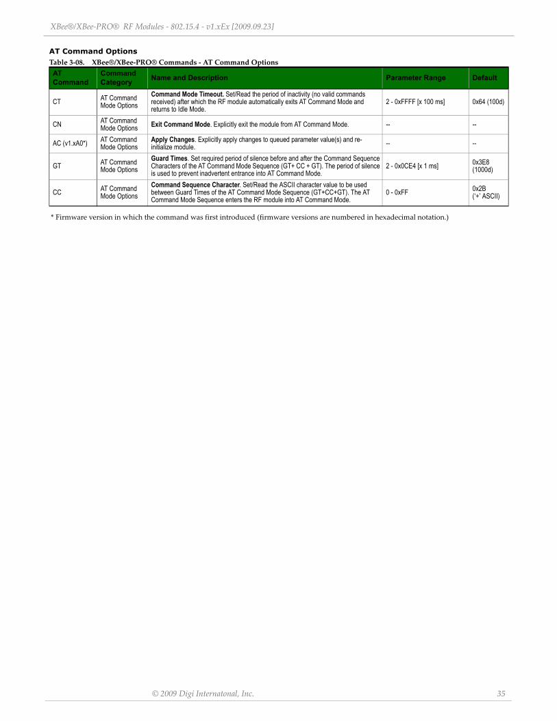
XBee®/XBee‐PRO® RF Modules ‐ 802.15.4 ‐ v1.xEx [2009.09.23]
© 2009 Digi Internatonal, Inc. 35
AT Command Options
* Firmware version in which the command was first introduced (firmware versions are numbered in hexadecimal notation.)
Table 3‐08. XBee®/XBee‐PRO® Commands ‐ AT Command OptionsAT Command
Command Category Name and Description Parameter Range Default
CT AT Command Mode Options
Command Mode Timeout. Set/Read the period of inactivity (no valid commands received) after which the RF module automatically exits AT Command Mode and returns to Idle Mode.
2 - 0xFFFF [x 100 ms] 0x64 (100d)
CN AT Command Mode Options Exit Command Mode. Explicitly exit the module from AT Command Mode. -- --
AC (v1.xA0*) AT Command Mode Options
Apply Changes. Explicitly apply changes to queued parameter value(s) and re-initialize module. -- --
GT AT Command Mode Options
Guard Times. Set required period of silence before and after the Command Sequence Characters of the AT Command Mode Sequence (GT+ CC + GT). The period of silence is used to prevent inadvertent entrance into AT Command Mode.
2 - 0x0CE4 [x 1 ms] 0x3E8 (1000d)
CC AT Command Mode Options
Command Sequence Character. Set/Read the ASCII character value to be used between Guard Times of the AT Command Mode Sequence (GT+CC+GT). The AT Command Mode Sequence enters the RF module into AT Command Mode.
0 - 0xFF 0x2B (‘+’ ASCII)
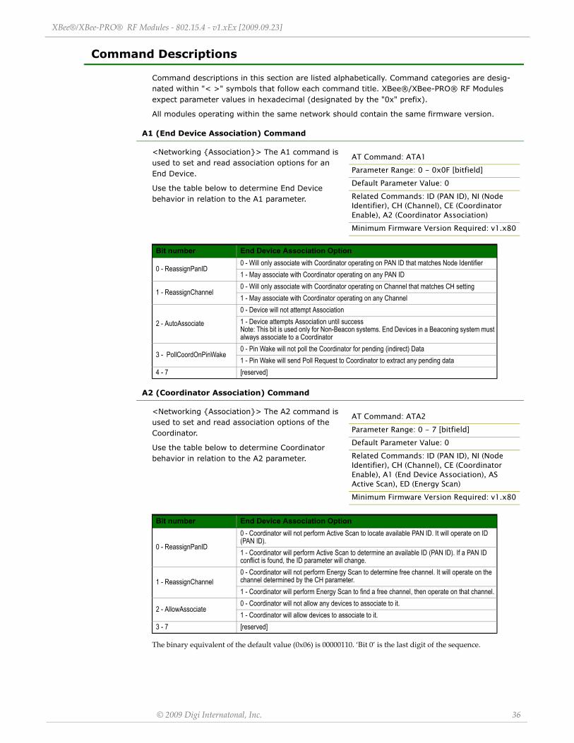
XBee®/XBee‐PRO® RF Modules ‐ 802.15.4 ‐ v1.xEx [2009.09.23]
© 2009 Digi Internatonal, Inc. 36
Command Descriptions
Command descriptions in this section are listed alphabetically. Command categories are desig-nated within "< >" symbols that follow each command title. XBee®/XBee-PRO® RF Modules expect parameter values in hexadecimal (designated by the "0x" prefix).
All modules operating within the same network should contain the same firmware version.
A1 (End Device Association) Command
<Networking Association> The A1 command is used to set and read association options for an End Device.
Use the table below to determine End Device behavior in relation to the A1 parameter.
A2 (Coordinator Association) Command
<Networking Association> The A2 command is used to set and read association options of the Coordinator.
Use the table below to determine Coordinator behavior in relation to the A2 parameter.
The binary equivalent of the default value (0x06) is 00000110. ‘Bit 0’ is the last digit of the sequence.
Bit number End Device Association Option
0 - ReassignPanID0 - Will only associate with Coordinator operating on PAN ID that matches Node Identifier1 - May associate with Coordinator operating on any PAN ID
1 - ReassignChannel0 - Will only associate with Coordinator operating on Channel that matches CH setting1 - May associate with Coordinator operating on any Channel
2 - AutoAssociate
0 - Device will not attempt Association1 - Device attempts Association until success Note: This bit is used only for Non-Beacon systems. End Devices in a Beaconing system must always associate to a Coordinator
3 - PollCoordOnPinWake0 - Pin Wake will not poll the Coordinator for pending (indirect) Data1 - Pin Wake will send Poll Request to Coordinator to extract any pending data
4 - 7 [reserved]
Bit number End Device Association Option
0 - ReassignPanID
0 - Coordinator will not perform Active Scan to locate available PAN ID. It will operate on ID (PAN ID). 1 - Coordinator will perform Active Scan to determine an available ID (PAN ID). If a PAN ID conflict is found, the ID parameter will change.
1 - ReassignChannel0 - Coordinator will not perform Energy Scan to determine free channel. It will operate on the channel determined by the CH parameter.1 - Coordinator will perform Energy Scan to find a free channel, then operate on that channel.
2 - AllowAssociate0 - Coordinator will not allow any devices to associate to it.1 - Coordinator will allow devices to associate to it.
3 - 7 [reserved]
AT Command: ATA1Parameter Range: 0 - 0x0F [bitfield]Default Parameter Value: 0Related Commands: ID (PAN ID), NI (Node Identifier), CH (Channel), CE (Coordinator Enable), A2 (Coordinator Association)Minimum Firmware Version Required: v1.x80
AT Command: ATA2Parameter Range: 0 - 7 [bitfield]Default Parameter Value: 0Related Commands: ID (PAN ID), NI (Node Identifier), CH (Channel), CE (Coordinator Enable), A1 (End Device Association), AS Active Scan), ED (Energy Scan)Minimum Firmware Version Required: v1.x80
XBee®/XBee‐PRO® RF Modules ‐ 802.15.4 ‐ v1.xEx [2009.09.23]
© 2009 Digi Internatonal, Inc. 37
AC (Apply Changes) Command
<AT Command Mode Options> The AC command is used to explicitly apply changes to module parameter values. ‘Applying changes’ means that the module is re-initialized based on changes made to its parameter values. Once changes are applied, the module immediately operates according to the new parameter values.
This behavior is in contrast to issuing the WR (Write) command. The WR command saves parame-ter values to non-volatile memory, but the module still operates according to previously saved val-ues until the module is re-booted or the CN (Exit AT Command Mode) command is issued.
Refer to the “AT Command - Queue Parameter Value” API type for more information.
AI (Association Indication) Command
<Networking Association> The AI command is used to indicate occurrences of errors during the last association request.
Use the table below to determine meaning of the returned values.
Returned Value (Hex) Association Indication0x00 Successful Completion - Coordinator successfully started or End Device association complete0x01 Active Scan Timeout0x02 Active Scan found no PANs0x03 Active Scan found PAN, but the Coordinator Allow Association bit is not set0x04 Active Scan found PAN, but Coordinator and End Device are not configured to support beacons0x05 Active Scan found PAN, but Coordinator ID (PAN ID) value does not match the ID of the End Device0x06 Active Scan found PAN, but Coordinator CH (Channel) value does not match the CH of the End Device0x07 Energy Scan Timeout0x08 Coordinator start request failed0x09 Coordinator could not start due to Invalid Parameter0x0A Coordinator Realignment is in progress0x0B Association Request not sent0x0C Association Request timed out - no reply was received0x0D Association Request had an Invalid Parameter0x0E Association Request Channel Access Failure - Request was not transmitted - CCA failure0x0F Remote Coordinator did not send an ACK after Association Request was sent
0x10 Remote Coordinator did not reply to the Association Request, but an ACK was received after sending the request
0x11 [reserved]0x12 Sync-Loss - Lost synchronization with a Beaconing Coordinator0x13 Disassociated - No longer associated to Coordinator0xFF RF Module is attempting to associate
AT Command: ATACMinimum Firmware Version Required: v1.xA0
AT Command: ATAIParameter Range: 0 - 0x13 [read-only]Related Commands: AS (Active Scan), ID (PAN ID), CH (Channel), ED (Energy Scan), A1 (End Device Association), A2 (Coordinator Association), CE (Coordinator Enable)Minimum Firmware Version Required: v1.x80
XBee®/XBee‐PRO® RF Modules ‐ 802.15.4 ‐ v1.xEx [2009.09.23]
© 2009 Digi Internatonal, Inc. 38
AP (API Enable) Command
<Serial Interfacing> The AP command is used to enable the RF module to operate using a frame-based API instead of using the default Transpar-ent (UART) mode.
Refer to the API Operation section when API operation is enabled (AP = 1 or 2).
AS (Active Scan) Command
<Network Association> The AS command is used to send a Beacon Request to a Broadcast (0xFFFF) and Broadcast PAN (0xFFFF) on every channel. The parameter determines the amount of time the RF module will listen for Beacons on each channel. A ‘PanDescriptor’ is created and returned for every Beacon received from the scan. Each PanDescriptor contains the following information:
CoordAddress (SH + SL parameters)<CR> (NOTE: If MY on the coordinator is set less than 0xFFFF, the MY value is displayed) CoordPanID (ID parameter)<CR> CoordAddrMode <CR>
0x02 = 16-bit Short Address 0x03 = 64-bit Long Address
Channel (CH parameter) <CR> SecurityUse<CR> ACLEntry<CR> SecurityFailure<CR> SuperFrameSpec<CR> (2 bytes):
bit 15 - Association Permitted (MSB) bit 14 - PAN Coordinator bit 13 - Reserved bit 12 - Battery Life Extension bits 8-11 - Final CAP Slot bits 4-7 - Superframe Order bits 0-3 - Beacon Order
GtsPermit<CR> RSSI<CR> (- RSSI is returned as -dBm) TimeStamp<CR> (3 bytes) <CR> (A carriage return <CR> is sent at the end of the AS command.
The Active Scan is capable of returning up to 5 PanDescriptors in a scan. The actual scan time on each channel is measured as Time = [(2 ^ (SD Parameter)) * 15.36] ms. Total scan time is this time multiplied by the number of channels to be scanned (16 for the XBee, 12 for the XBee-PRO).
AT Command: ATAPParameter Range:0 - 2
Parameter Configuration
0 Disabled(Transparent operation)
1 API enabled
2 API enabled (with escaped characters)
Default Parameter Value:0Minimum Firmware Version Required: v1.x80
AT Command: ATASParameter Range: 0 - 6Related Command: SD (Scan Duration), DL (Destination Low Address), DH (Destination High Address), ID (PAN ID), CH (Channel)Minimum Firmware Version Required: v1.x80
XBee®/XBee‐PRO® RF Modules ‐ 802.15.4 ‐ v1.xEx [2009.09.23]
© 2009 Digi Internatonal, Inc. 39
NOTE: Refer the scan table in the SD description to determine scan times. If using API Mode, no <CR>’s are returned in the response. Refer to the API Mode Operation section.
BD (Interface Data Rate) Command
<Serial Interfacing> The BD command is used to set and read the serial interface data rate used between the RF module and host. This parameter determines the rate at which serial data is sent to the module from the host. Modified interface data rates do not take effect until the CN (Exit AT Com-mand Mode) command is issued and the system returns the 'OK' response.
When parameters 0-7 are sent to the module, the respective interface data rates are used (as shown in the table on the right).
The RF data rate is not affected by the BD param-eter. If the interface data rate is set higher than the RF data rate, a flow control configuration may need to be implemented.
Non-standard Interface Data Rates: Any value above 0x07 will be interpreted as an actual baud rate. When a value above 0x07 is sent, the closest interface data rate represented by the number is stored in the BD register. For exam-ple, a rate of 19200 bps can be set by sending the following command line "ATBD4B00". NOTE: When using Digi’s X-CTU Software, non-standard interface data rates can only be set and read using the X-CTU ‘Terminal’ tab. Non-standard rates are not accessible through the ‘Modem Config-uration’ tab.
When the BD command is sent with a non-standard interface data rate, the UART will adjust to accommodate the requested interface rate. In most cases, the clock resolution will cause the stored BD parameter to vary from the parameter that was sent (refer to the table below). Reading the BD command (send "ATBD" command without an associated parameter value) will return the value actually stored in the module’s BD register.
* The 115,200 baud rate setting is actually at 111,111 baud (-3.5% target UART speed).
CA (CCA Threshold) Command
<RF Interfacing> CA command is used to set and read CCA (Clear Channel Assessment) thresholds.
Prior to transmitting a packet, a CCA is performed to detect energy on the transmit channel. If the detected energy is above the CCA Threshold, the RF module will not transmit the packet.
Parameters Sent Versus Parameters Stored
BD Parameter Sent (HEX) Interface Data Rate (bps) BD Parameter Stored (HEX)0 1200 04 19,200 47 115,200* 7
12C 300 12B1C200 115,200 1B207
AT Command: ATBDParameter Range:0 - 7 (standard rates) 0x80-0x3D090 (non-standard rates up to 250 Kbps)
Parameter Configuration (bps)0 12001 24002 48003 96004 192005 384006 576007 115200
Default Parameter Value:3
AT Command: ATCAParameter Range: 0 - 0x50 [-dBm]Default Parameter Value: 0x2C
(-44 decimal dBm)Minimum Firmware Version Required: v1.x80
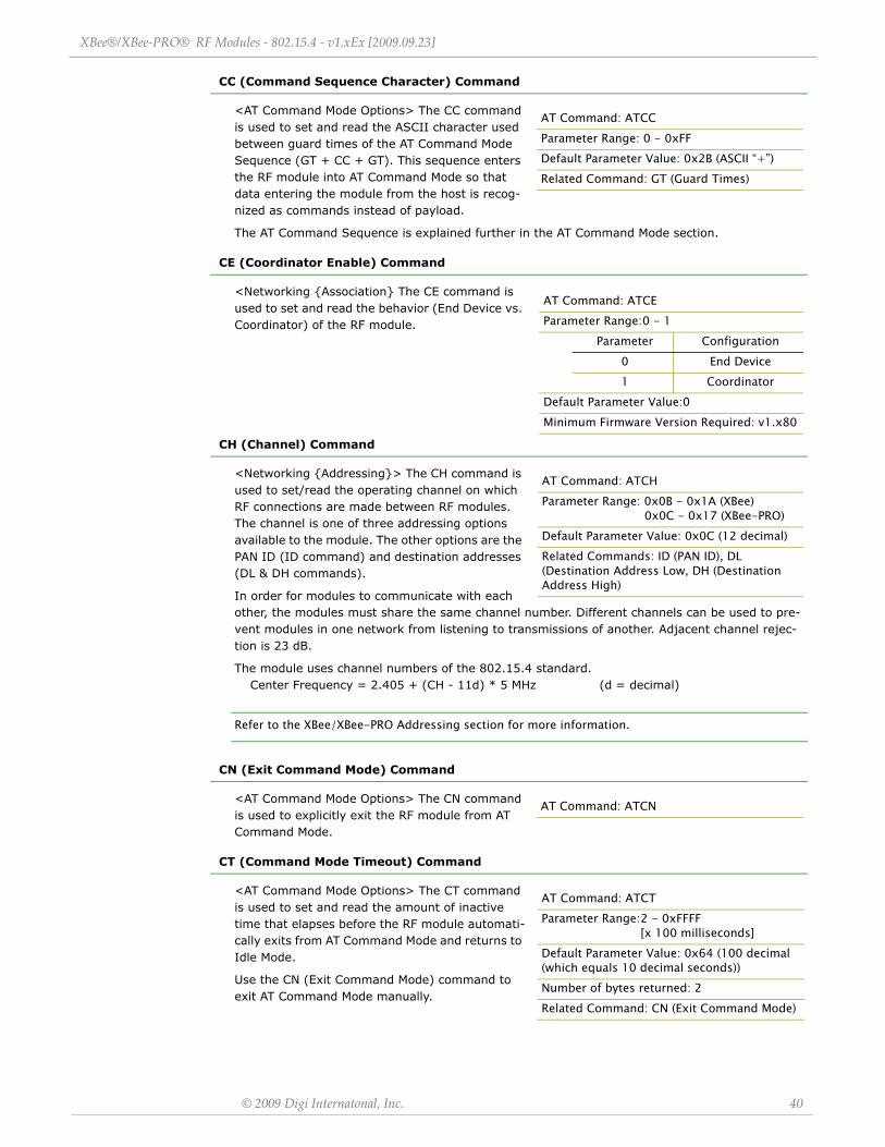
XBee®/XBee‐PRO® RF Modules ‐ 802.15.4 ‐ v1.xEx [2009.09.23]
© 2009 Digi Internatonal, Inc. 40
CC (Command Sequence Character) Command
<AT Command Mode Options> The CC command is used to set and read the ASCII character used between guard times of the AT Command Mode Sequence (GT + CC + GT). This sequence enters the RF module into AT Command Mode so that data entering the module from the host is recog-nized as commands instead of payload.
The AT Command Sequence is explained further in the AT Command Mode section.
CE (Coordinator Enable) Command
<Networking Association The CE command is used to set and read the behavior (End Device vs. Coordinator) of the RF module.
CH (Channel) Command
<Networking Addressing> The CH command is used to set/read the operating channel on which RF connections are made between RF modules. The channel is one of three addressing options available to the module. The other options are the PAN ID (ID command) and destination addresses (DL & DH commands).
In order for modules to communicate with each other, the modules must share the same channel number. Different channels can be used to pre-vent modules in one network from listening to transmissions of another. Adjacent channel rejec-tion is 23 dB.
The module uses channel numbers of the 802.15.4 standard. Center Frequency = 2.405 + (CH - 11d) * 5 MHz (d = decimal)
Refer to the XBee/XBee-PRO Addressing section for more information.
CN (Exit Command Mode) Command
<AT Command Mode Options> The CN command is used to explicitly exit the RF module from AT Command Mode.
CT (Command Mode Timeout) Command
<AT Command Mode Options> The CT command is used to set and read the amount of inactive time that elapses before the RF module automati-cally exits from AT Command Mode and returns to Idle Mode.
Use the CN (Exit Command Mode) command to exit AT Command Mode manually.
AT Command: ATCCParameter Range: 0 - 0xFFDefault Parameter Value: 0x2B (ASCII “+”)Related Command: GT (Guard Times)
AT Command: ATCEParameter Range:0 - 1
Parameter Configuration0 End Device1 Coordinator
Default Parameter Value:0Minimum Firmware Version Required: v1.x80
AT Command: ATCHParameter Range: 0x0B - 0x1A (XBee)
0x0C - 0x17 (XBee-PRO)Default Parameter Value: 0x0C (12 decimal)Related Commands: ID (PAN ID), DL (Destination Address Low, DH (Destination Address High)
AT Command: ATCN
AT Command: ATCTParameter Range:2 - 0xFFFF
[x 100 milliseconds]Default Parameter Value: 0x64 (100 decimal (which equals 10 decimal seconds))Number of bytes returned: 2Related Command: CN (Exit Command Mode)
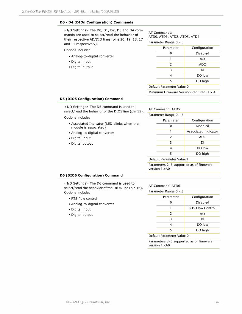
XBee®/XBee‐PRO® RF Modules ‐ 802.15.4 ‐ v1.xEx [2009.09.23]
© 2009 Digi Internatonal, Inc. 41
D0 - D4 (DIOn Configuration) Commands
<I/O Settings> The D0, D1, D2, D3 and D4 com-mands are used to select/read the behavior of their respective AD/DIO lines (pins 20, 19, 18, 17 and 11 respectively).
Options include:
• Analog-to-digital converter
• Digital input
• Digital output
D5 (DIO5 Configuration) Command
<I/O Settings> The D5 command is used to select/read the behavior of the DIO5 line (pin 15).
Options include:
• Associated Indicator (LED blinks when the module is associated)
• Analog-to-digital converter
• Digital input
• Digital output
D6 (DIO6 Configuration) Command
<I/O Settings> The D6 command is used to select/read the behavior of the DIO6 line (pin 16). Options include:
• RTS flow control
• Analog-to-digital converter
• Digital input
• Digital output
AT Commands: ATD0, ATD1, ATD2, ATD3, ATD4Parameter Range:0 - 5
Parameter Configuration0 Disabled1 n/a2 ADC3 DI4 DO low5 DO high
Default Parameter Value:0Minimum Firmware Version Required: 1.x.A0
AT Command: ATD5Parameter Range:0 - 5
Parameter Configuration0 Disabled1 Associated Indicator2 ADC3 DI4 DO low5 DO high
Default Parameter Value:1Parameters 2-5 supported as of firmware version 1.xA0
AT Command: ATD6Parameter Range:0 - 5
Parameter Configuration0 Disabled1 RTS Flow Control2 n/a3 DI4 DO low5 DO high
Default Parameter Value:0Parameters 3-5 supported as of firmware version 1.xA0
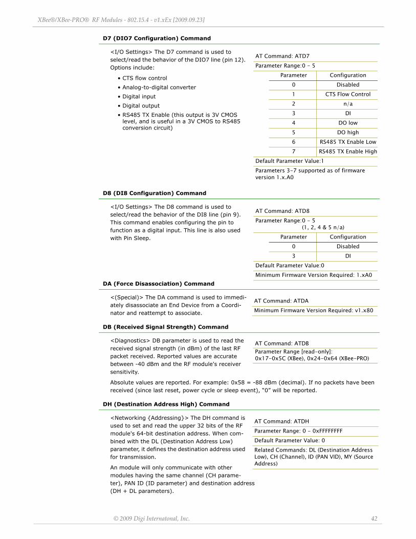
XBee®/XBee‐PRO® RF Modules ‐ 802.15.4 ‐ v1.xEx [2009.09.23]
© 2009 Digi Internatonal, Inc. 42
D7 (DIO7 Configuration) Command
<I/O Settings> The D7 command is used to select/read the behavior of the DIO7 line (pin 12). Options include:
• CTS flow control
• Analog-to-digital converter
• Digital input
• Digital output
• RS485 TX Enable (this output is 3V CMOS level, and is useful in a 3V CMOS to RS485 conversion circuit)
D8 (DI8 Configuration) Command
<I/O Settings> The D8 command is used to select/read the behavior of the DI8 line (pin 9). This command enables configuring the pin to function as a digital input. This line is also used with Pin Sleep.
DA (Force Disassociation) Command
<(Special)> The DA command is used to immedi-ately disassociate an End Device from a Coordi-nator and reattempt to associate.
DB (Received Signal Strength) Command
<Diagnostics> DB parameter is used to read the received signal strength (in dBm) of the last RF packet received. Reported values are accurate between -40 dBm and the RF module's receiver sensitivity.
Absolute values are reported. For example: 0x58 = -88 dBm (decimal). If no packets have been received (since last reset, power cycle or sleep event), “0” will be reported.
DH (Destination Address High) Command
<Networking Addressing> The DH command is used to set and read the upper 32 bits of the RF module's 64-bit destination address. When com-bined with the DL (Destination Address Low) parameter, it defines the destination address used for transmission.
An module will only communicate with other modules having the same channel (CH parame-ter), PAN ID (ID parameter) and destination address (DH + DL parameters).
AT Command: ATD7Parameter Range:0 - 5
Parameter Configuration0 Disabled1 CTS Flow Control2 n/a3 DI4 DO low5 DO high6 RS485 TX Enable Low7 RS485 TX Enable High
Default Parameter Value:1Parameters 3-7 supported as of firmware version 1.x.A0
AT Command: ATD8Parameter Range:0 - 5
(1, 2, 4 & 5 n/a)Parameter Configuration
0 Disabled3 DI
Default Parameter Value:0Minimum Firmware Version Required: 1.xA0
AT Command: ATDAMinimum Firmware Version Required: v1.x80
AT Command: ATDBParameter Range [read-only]: 0x17-0x5C (XBee), 0x24-0x64 (XBee-PRO)
AT Command: ATDHParameter Range: 0 - 0xFFFFFFFFDefault Parameter Value: 0Related Commands: DL (Destination Address Low), CH (Channel), ID (PAN VID), MY (Source Address)
XBee®/XBee‐PRO® RF Modules ‐ 802.15.4 ‐ v1.xEx [2009.09.23]
© 2009 Digi Internatonal, Inc. 43
To transmit using a 16-bit address, set the DH parameter to zero and the DL parameter less than 0xFFFF. 0x000000000000FFFF (DL concatenated to DH) is the broadcast address for the PAN.
Refer to the XBee/XBee-PRO Addressing section for more information.
DL (Destination Address Low) Command
<Networking Addressing> The DL command is used to set and read the lower 32 bits of the RF module's 64-bit destination address. When com-bined with the DH (Destination Address High) parameter, it defines the destination address used for transmission.
A module will only communicate with other mod-ules having the same channel (CH parameter), PAN ID (ID parameter) and destination address (DH + DL parameters).
To transmit using a 16-bit address, set the DH parameter to zero and the DL parameter less than 0xFFFF. 0x000000000000FFFF (DL concatenated to DH) is the broadcast address for the PAN.
Refer to the XBee/XBee-PRO Addressing section for more information.
DN (Destination Node) Command
<Networking Identification> The DN command is used to resolve a NI (Node Identifier) string to a physical address. The following events occur upon successful command execution:
1. DL and DH are set to the address of the module with the matching NI (Node Identifier).
2. ‘OK’ is returned. 3. RF module automatically exits AT Command Mode.
If there is no response from a modem within 200 msec or a parameter is not specified (left blank), the command is terminated and an ‘ERROR’ message is returned.
DP (Disassociation Cyclic Sleep Period) Command
<Sleep Mode (Low Power)>
NonBeacon Firmware
End Device - The DP command is used to set and read the time period of sleep for cyclic sleeping remotes that are configured for Association but are not associated to a Coordinator. (i.e. If a device is configured to associate, configured as a Cyclic Sleep remote, but does not find a Coordi-nator; it will sleep for DP time before reattempt-ing association.) Maximum sleep period is 268 seconds (0x68B0). DP should be > 0 for NonBeacon systems.
EA (ACK Failures) Command
<Diagnostics> The EA command is used to reset and read the count of ACK (acknowledgement) failures. This parameter value increments when the module expires its transmission retries with-out receiving an ACK on a packet transmission. This count saturates at its maximum value.
Set the parameter to “0” to reset count.
AT Command: ATDLParameter Range: 0 - 0xFFFFFFFF
Default Parameter Value: 0Related Commands: DH (Destination Address High), CH (Channel), ID (PAN VID), MY (Source Address)
AT Command: ATDNParameter Range: 20-character ASCII StringMinimum Firmware Version Required: v1.x80
AT Command: ATDPParameter Range: 1 - 0x68B0
[x 10 milliseconds]Default Parameter Value:0x3E8
(1000 decimal)Related Commands: SM (Sleep Mode), SP (Cyclic Sleep Period), ST (Time before Sleep)Minimum Firmware Version Required: v1.x80
AT Command: ATEAParameter Range:0 - 0xFFFFMinimum Firmware Version Required: v1.x80
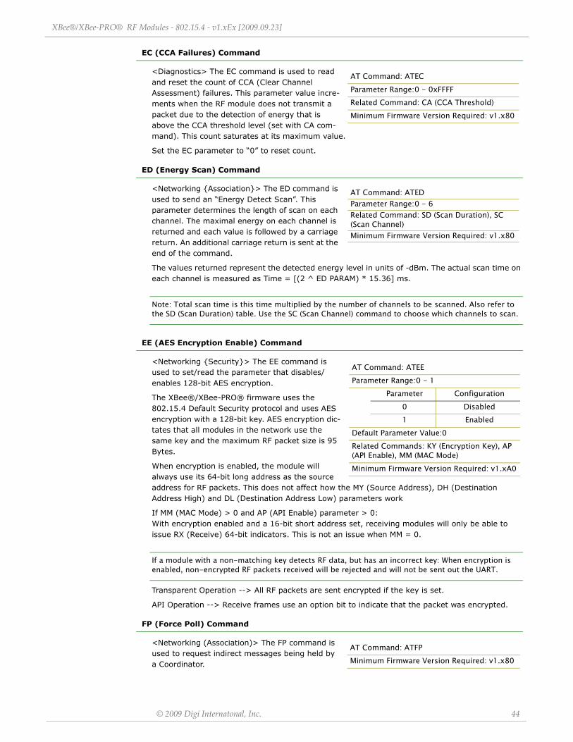
XBee®/XBee‐PRO® RF Modules ‐ 802.15.4 ‐ v1.xEx [2009.09.23]
© 2009 Digi Internatonal, Inc. 44
EC (CCA Failures) Command
<Diagnostics> The EC command is used to read and reset the count of CCA (Clear Channel Assessment) failures. This parameter value incre-ments when the RF module does not transmit a packet due to the detection of energy that is above the CCA threshold level (set with CA com-mand). This count saturates at its maximum value.
Set the EC parameter to “0” to reset count.
ED (Energy Scan) Command
<Networking Association> The ED command is used to send an “Energy Detect Scan”. This parameter determines the length of scan on each channel. The maximal energy on each channel is returned and each value is followed by a carriage return. An additional carriage return is sent at the end of the command.
The values returned represent the detected energy level in units of -dBm. The actual scan time on each channel is measured as Time = [(2 ^ ED PARAM) * 15.36] ms.
Note: Total scan time is this time multiplied by the number of channels to be scanned. Also refer to the SD (Scan Duration) table. Use the SC (Scan Channel) command to choose which channels to scan.
EE (AES Encryption Enable) Command
<Networking Security> The EE command is used to set/read the parameter that disables/enables 128-bit AES encryption.
The XBee®/XBee-PRO® firmware uses the 802.15.4 Default Security protocol and uses AES encryption with a 128-bit key. AES encryption dic-tates that all modules in the network use the same key and the maximum RF packet size is 95 Bytes.
When encryption is enabled, the module will always use its 64-bit long address as the source address for RF packets. This does not affect how the MY (Source Address), DH (Destination Address High) and DL (Destination Address Low) parameters work
If MM (MAC Mode) > 0 and AP (API Enable) parameter > 0: With encryption enabled and a 16-bit short address set, receiving modules will only be able to issue RX (Receive) 64-bit indicators. This is not an issue when MM = 0.
If a module with a non-matching key detects RF data, but has an incorrect key: When encryption is enabled, non-encrypted RF packets received will be rejected and will not be sent out the UART.
Transparent Operation --> All RF packets are sent encrypted if the key is set.
API Operation --> Receive frames use an option bit to indicate that the packet was encrypted.
FP (Force Poll) Command
<Networking (Association)> The FP command is used to request indirect messages being held by a Coordinator.
AT Command: ATECParameter Range:0 - 0xFFFFRelated Command: CA (CCA Threshold)Minimum Firmware Version Required: v1.x80
AT Command: ATEDParameter Range:0 - 6Related Command: SD (Scan Duration), SC (Scan Channel)Minimum Firmware Version Required: v1.x80
AT Command: ATEEParameter Range:0 - 1
Parameter Configuration0 Disabled1 Enabled
Default Parameter Value:0Related Commands: KY (Encryption Key), AP (API Enable), MM (MAC Mode)Minimum Firmware Version Required: v1.xA0
AT Command: ATFPMinimum Firmware Version Required: v1.x80
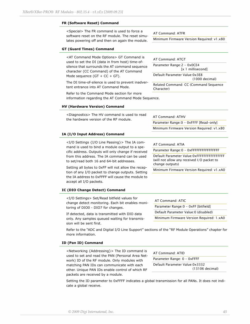
XBee®/XBee‐PRO® RF Modules ‐ 802.15.4 ‐ v1.xEx [2009.09.23]
© 2009 Digi Internatonal, Inc. 45
FR (Software Reset) Command
<Special> The FR command is used to force a software reset on the RF module. The reset simu-lates powering off and then on again the module.
GT (Guard Times) Command
<AT Command Mode Options> GT Command is used to set the DI (data in from host) time-of-silence that surrounds the AT command sequence character (CC Command) of the AT Command Mode sequence (GT + CC + GT).
The DI time-of-silence is used to prevent inadver-tent entrance into AT Command Mode.
Refer to the Command Mode section for more information regarding the AT Command Mode Sequence.
HV (Hardware Version) Command
<Diagnostics> The HV command is used to read the hardware version of the RF module.
IA (I/O Input Address) Command
<I/O Settings I/O Line Passing> The IA com-mand is used to bind a module output to a spe-cific address. Outputs will only change if received from this address. The IA command can be used to set/read both 16 and 64-bit addresses.
Setting all bytes to 0xFF will not allow the recep-tion of any I/O packet to change outputs. Setting the IA address to 0xFFFF will cause the module to accept all I/O packets.
IC (DIO Change Detect) Command
<I/O Settings> Set/Read bitfield values for change detect monitoring. Each bit enables moni-toring of DIO0 - DIO7 for changes.
If detected, data is transmitted with DIO data only. Any samples queued waiting for transmis-sion will be sent first.
Refer to the “ADC and Digital I/O Line Support” sections of the “RF Module Operations” chapter for more information.
ID (Pan ID) Command
<Networking Addressing> The ID command is used to set and read the PAN (Personal Area Net-work) ID of the RF module. Only modules with matching PAN IDs can communicate with each other. Unique PAN IDs enable control of which RF packets are received by a module.
Setting the ID parameter to 0xFFFF indicates a global transmission for all PANs. It does not indi-cate a global receive.
AT Command: ATFRMinimum Firmware Version Required: v1.x80
AT Command: ATGTParameter Range:2 - 0x0CE4
[x 1 millisecond]Default Parameter Value:0x3E8
(1000 decimal)Related Command: CC (Command Sequence Character)
AT Command: ATHVParameter Range:0 - 0xFFFF [Read-only]Minimum Firmware Version Required: v1.x80
AT Command: ATIAParameter Range:0 - 0xFFFFFFFFFFFFFFFFDefault Parameter Value:0xFFFFFFFFFFFFFFFF (will not allow any received I/O packet to change outputs)Minimum Firmware Version Required: v1.xA0
AT Command: ATICParameter Range:0 - 0xFF [bitfield]Default Parameter Value:0 (disabled)Minimum Firmware Version Required: 1.xA0
AT Command: ATIDParameter Range: 0 - 0xFFFFDefault Parameter Value:0x3332
(13106 decimal)
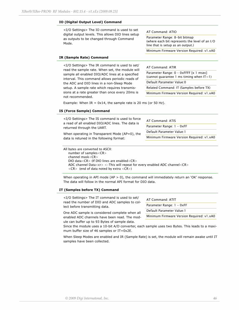
XBee®/XBee‐PRO® RF Modules ‐ 802.15.4 ‐ v1.xEx [2009.09.23]
© 2009 Digi Internatonal, Inc. 46
IO (Digital Output Level) Command
<I/O Settings> The IO command is used to set digital output levels. This allows DIO lines setup as outputs to be changed through Command Mode.
IR (Sample Rate) Command
<I/O Settings> The IR command is used to set/read the sample rate. When set, the module will sample all enabled DIO/ADC lines at a specified interval. This command allows periodic reads of the ADC and DIO lines in a non-Sleep Mode setup. A sample rate which requires transmis-sions at a rate greater than once every 20ms is not recommended.
Example: When IR = 0x14, the sample rate is 20 ms (or 50 Hz).
IS (Force Sample) Command
<I/O Settings> The IS command is used to force a read of all enabled DIO/ADC lines. The data is returned through the UART.
When operating in Transparent Mode (AP=0), the data is retuned in the following format:
All bytes are converted to ASCII: number of samples<CR> channel mask<CR> DIO data<CR> (If DIO lines are enabled<CR> ADC channel Data<cr> <-This will repeat for every enabled ADC channel<CR> <CR> (end of data noted by extra <CR>)
When operating in API mode (AP > 0), the command will immediately return an ‘OK’ response. The data will follow in the normal API format for DIO data.
IT (Samples before TX) Command
<I/O Settings> The IT command is used to set/read the number of DIO and ADC samples to col-lect before transmitting data.
One ADC sample is considered complete when all enabled ADC channels have been read. The mod-ule can buffer up to 93 Bytes of sample data. Since the module uses a 10-bit A/D converter, each sample uses two Bytes. This leads to a maxi-mum buffer size of 46 samples or IT=0x2E.
When Sleep Modes are enabled and IR (Sample Rate) is set, the module will remain awake until IT samples have been collected.
AT Command: ATIOParameter Range: 8-bit bitmap (where each bit represents the level of an I/O line that is setup as an output.)Minimum Firmware Version Required: v1.xA0
AT Command: ATIRParameter Range: 0 - 0xFFFF [x 1 msec] (cannot guarantee 1 ms timing when IT=1)Default Parameter Value:0Related Command: IT (Samples before TX)Minimum Firmware Version Required: v1.xA0
AT Command: ATISParameter Range: 1 - 0xFFDefault Parameter Value:1Minimum Firmware Version Required: v1.xA0
AT Command: ATITParameter Range: 1 - 0xFFDefault Parameter Value:1Minimum Firmware Version Required: v1.xA0
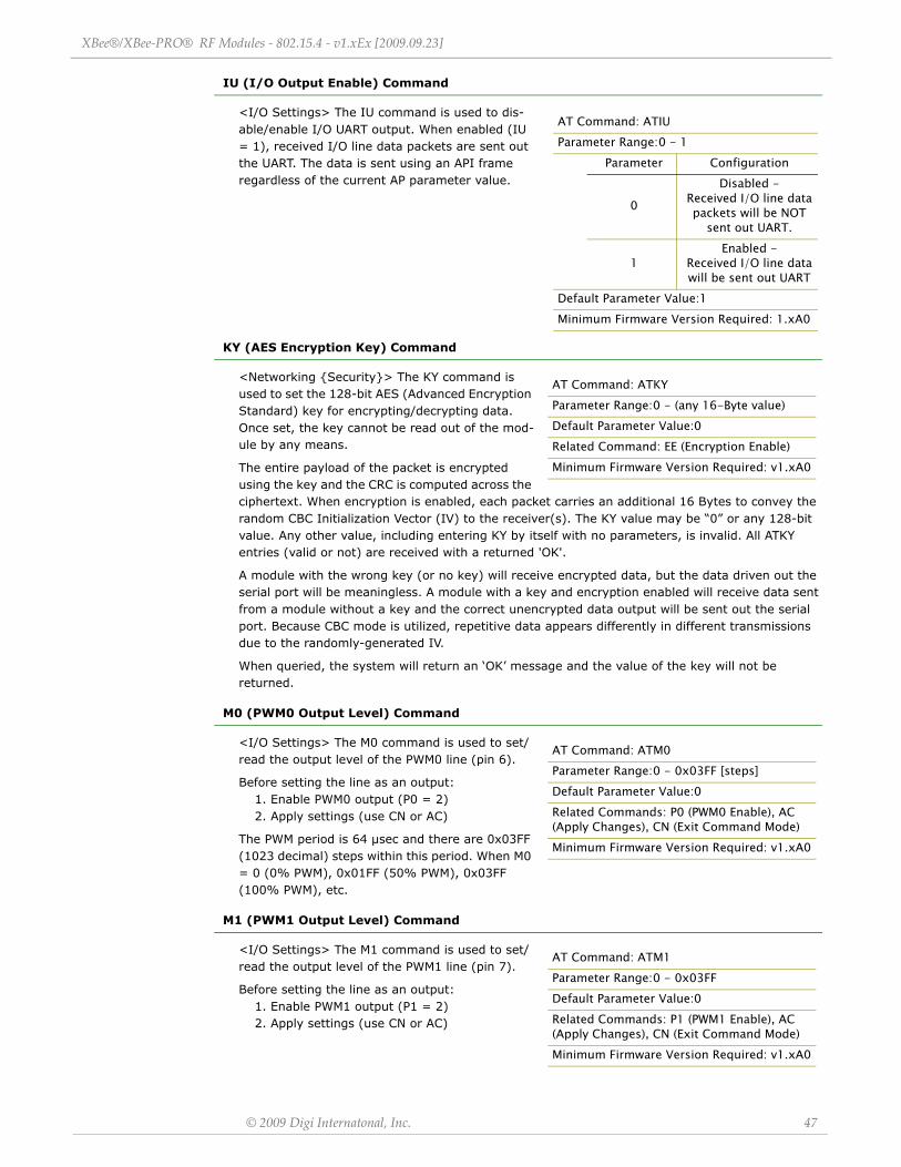
XBee®/XBee‐PRO® RF Modules ‐ 802.15.4 ‐ v1.xEx [2009.09.23]
© 2009 Digi Internatonal, Inc. 47
IU (I/O Output Enable) Command
<I/O Settings> The IU command is used to dis-able/enable I/O UART output. When enabled (IU = 1), received I/O line data packets are sent out the UART. The data is sent using an API frame regardless of the current AP parameter value.
KY (AES Encryption Key) Command
<Networking Security> The KY command is used to set the 128-bit AES (Advanced Encryption Standard) key for encrypting/decrypting data. Once set, the key cannot be read out of the mod-ule by any means.
The entire payload of the packet is encrypted using the key and the CRC is computed across the ciphertext. When encryption is enabled, each packet carries an additional 16 Bytes to convey the random CBC Initialization Vector (IV) to the receiver(s). The KY value may be “0” or any 128-bit value. Any other value, including entering KY by itself with no parameters, is invalid. All ATKY entries (valid or not) are received with a returned 'OK'.
A module with the wrong key (or no key) will receive encrypted data, but the data driven out the serial port will be meaningless. A module with a key and encryption enabled will receive data sent from a module without a key and the correct unencrypted data output will be sent out the serial port. Because CBC mode is utilized, repetitive data appears differently in different transmissions due to the randomly-generated IV.
When queried, the system will return an ‘OK’ message and the value of the key will not be returned.
M0 (PWM0 Output Level) Command
<I/O Settings> The M0 command is used to set/read the output level of the PWM0 line (pin 6).
Before setting the line as an output: 1. Enable PWM0 output (P0 = 2) 2. Apply settings (use CN or AC)
The PWM period is 64 µsec and there are 0x03FF (1023 decimal) steps within this period. When M0 = 0 (0% PWM), 0x01FF (50% PWM), 0x03FF (100% PWM), etc.
M1 (PWM1 Output Level) Command
<I/O Settings> The M1 command is used to set/read the output level of the PWM1 line (pin 7).
Before setting the line as an output: 1. Enable PWM1 output (P1 = 2) 2. Apply settings (use CN or AC)
AT Command: ATIUParameter Range:0 - 1
Parameter Configuration
0
Disabled - Received I/O line data packets will be NOT
sent out UART.
1Enabled -
Received I/O line data will be sent out UART
Default Parameter Value:1Minimum Firmware Version Required: 1.xA0
AT Command: ATKYParameter Range:0 - (any 16-Byte value)Default Parameter Value:0Related Command: EE (Encryption Enable)Minimum Firmware Version Required: v1.xA0
AT Command: ATM0Parameter Range:0 - 0x03FF [steps]Default Parameter Value:0Related Commands: P0 (PWM0 Enable), AC (Apply Changes), CN (Exit Command Mode)Minimum Firmware Version Required: v1.xA0
AT Command: ATM1Parameter Range:0 - 0x03FFDefault Parameter Value:0Related Commands: P1 (PWM1 Enable), AC (Apply Changes), CN (Exit Command Mode)Minimum Firmware Version Required: v1.xA0
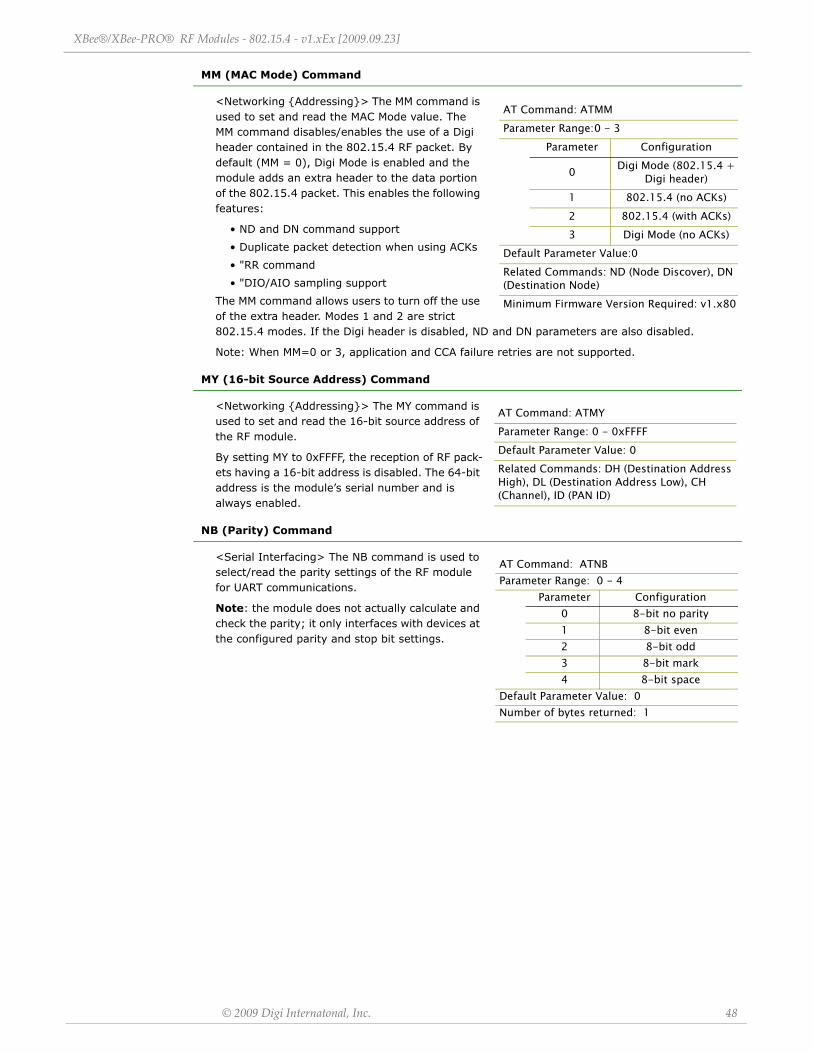
XBee®/XBee‐PRO® RF Modules ‐ 802.15.4 ‐ v1.xEx [2009.09.23]
© 2009 Digi Internatonal, Inc. 48
MM (MAC Mode) Command
<Networking Addressing> The MM command is used to set and read the MAC Mode value. The MM command disables/enables the use of a Digi header contained in the 802.15.4 RF packet. By default (MM = 0), Digi Mode is enabled and the module adds an extra header to the data portion of the 802.15.4 packet. This enables the following features:
• ND and DN command support
• Duplicate packet detection when using ACKs
• "RR command
• "DIO/AIO sampling support
The MM command allows users to turn off the use of the extra header. Modes 1 and 2 are strict 802.15.4 modes. If the Digi header is disabled, ND and DN parameters are also disabled.
Note: When MM=0 or 3, application and CCA failure retries are not supported.
MY (16-bit Source Address) Command
<Networking Addressing> The MY command is used to set and read the 16-bit source address of the RF module.
By setting MY to 0xFFFF, the reception of RF pack-ets having a 16-bit address is disabled. The 64-bit address is the module’s serial number and is always enabled.
NB (Parity) Command
<Serial Interfacing> The NB command is used to select/read the parity settings of the RF module for UART communications.
Note: the module does not actually calculate and check the parity; it only interfaces with devices at the configured parity and stop bit settings.
AT Command: ATMMParameter Range:0 - 3
Parameter Configuration
0 Digi Mode (802.15.4 + Digi header)
1 802.15.4 (no ACKs)2 802.15.4 (with ACKs)3 Digi Mode (no ACKs)
Default Parameter Value:0Related Commands: ND (Node Discover), DN (Destination Node) Minimum Firmware Version Required: v1.x80
AT Command: ATMYParameter Range: 0 - 0xFFFFDefault Parameter Value: 0Related Commands: DH (Destination Address High), DL (Destination Address Low), CH (Channel), ID (PAN ID)
AT Command: ATNBParameter Range: 0 - 4
Parameter Configuration0 8-bit no parity1 8-bit even2 8-bit odd3 8-bit mark4 8-bit space
Default Parameter Value: 0Number of bytes returned: 1
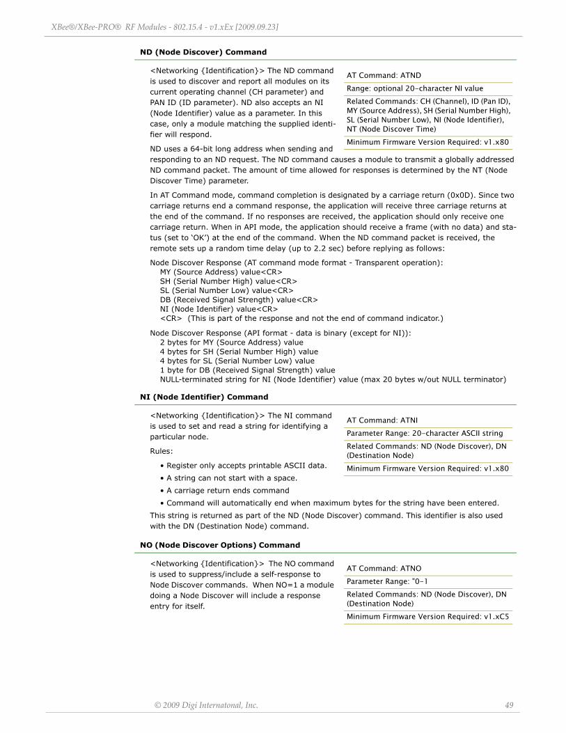
XBee®/XBee‐PRO® RF Modules ‐ 802.15.4 ‐ v1.xEx [2009.09.23]
© 2009 Digi Internatonal, Inc. 49
ND (Node Discover) Command
<Networking Identification> The ND command is used to discover and report all modules on its current operating channel (CH parameter) and PAN ID (ID parameter). ND also accepts an NI (Node Identifier) value as a parameter. In this case, only a module matching the supplied identi-fier will respond.
ND uses a 64-bit long address when sending and responding to an ND request. The ND command causes a module to transmit a globally addressed ND command packet. The amount of time allowed for responses is determined by the NT (Node Discover Time) parameter.
In AT Command mode, command completion is designated by a carriage return (0x0D). Since two carriage returns end a command response, the application will receive three carriage returns at the end of the command. If no responses are received, the application should only receive one carriage return. When in API mode, the application should receive a frame (with no data) and sta-tus (set to ‘OK’) at the end of the command. When the ND command packet is received, the remote sets up a random time delay (up to 2.2 sec) before replying as follows:
Node Discover Response (AT command mode format - Transparent operation): MY (Source Address) value<CR> SH (Serial Number High) value<CR> SL (Serial Number Low) value<CR> DB (Received Signal Strength) value<CR> NI (Node Identifier) value<CR> <CR> (This is part of the response and not the end of command indicator.)
Node Discover Response (API format - data is binary (except for NI)): 2 bytes for MY (Source Address) value 4 bytes for SH (Serial Number High) value 4 bytes for SL (Serial Number Low) value 1 byte for DB (Received Signal Strength) value NULL-terminated string for NI (Node Identifier) value (max 20 bytes w/out NULL terminator)
NI (Node Identifier) Command
<Networking Identification> The NI command is used to set and read a string for identifying a particular node.
Rules:
• Register only accepts printable ASCII data.
• A string can not start with a space.
• A carriage return ends command
• Command will automatically end when maximum bytes for the string have been entered.
This string is returned as part of the ND (Node Discover) command. This identifier is also used with the DN (Destination Node) command.
NO (Node Discover Options) Command
<Networking Identification> The NO command is used to suppress/include a self-response to Node Discover commands. When NO=1 a module doing a Node Discover will include a response entry for itself.
AT Command: ATNDRange: optional 20-character NI valueRelated Commands: CH (Channel), ID (Pan ID), MY (Source Address), SH (Serial Number High), SL (Serial Number Low), NI (Node Identifier), NT (Node Discover Time)Minimum Firmware Version Required: v1.x80
AT Command: ATNIParameter Range: 20-character ASCII stringRelated Commands: ND (Node Discover), DN (Destination Node)Minimum Firmware Version Required: v1.x80
AT Command: ATNOParameter Range: "0-1Related Commands: ND (Node Discover), DN (Destination Node)Minimum Firmware Version Required: v1.xC5
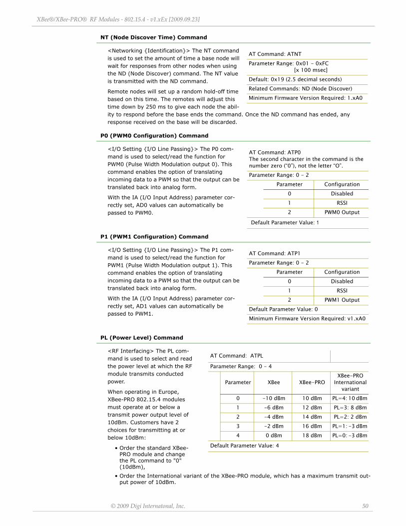
XBee®/XBee‐PRO® RF Modules ‐ 802.15.4 ‐ v1.xEx [2009.09.23]
© 2009 Digi Internatonal, Inc. 50
NT (Node Discover Time) Command
<Networking Identification> The NT command is used to set the amount of time a base node will wait for responses from other nodes when using the ND (Node Discover) command. The NT value is transmitted with the ND command.
Remote nodes will set up a random hold-off time based on this time. The remotes will adjust this time down by 250 ms to give each node the abil-ity to respond before the base ends the command. Once the ND command has ended, any response received on the base will be discarded.
P0 (PWM0 Configuration) Command
<I/O Setting I/O Line Passing> The P0 com-mand is used to select/read the function for PWM0 (Pulse Width Modulation output 0). This command enables the option of translating incoming data to a PWM so that the output can be translated back into analog form.
With the IA (I/O Input Address) parameter cor-rectly set, AD0 values can automatically be passed to PWM0.
P1 (PWM1 Configuration) Command
<I/O Setting I/O Line Passing> The P1 com-mand is used to select/read the function for PWM1 (Pulse Width Modulation output 1). This command enables the option of translating incoming data to a PWM so that the output can be translated back into analog form.
With the IA (I/O Input Address) parameter cor-rectly set, AD1 values can automatically be passed to PWM1.
PL (Power Level) Command
<RF Interfacing> The PL com-mand is used to select and read the power level at which the RF module transmits conducted power.
When operating in Europe, XBee-PRO 802.15.4 modules must operate at or below a transmit power output level of 10dBm. Customers have 2 choices for transmitting at or below 10dBm:
• Order the standard XBee-PRO module and change the PL command to "0" (10dBm),
• Order the International variant of the XBee-PRO module, which has a maximum transmit out-put power of 10dBm.
AT Command: ATNTParameter Range: 0x01 - 0xFC
[x 100 msec]Default: 0x19 (2.5 decimal seconds)Related Commands: ND (Node Discover)Minimum Firmware Version Required: 1.xA0
AT Command: ATP0 The second character in the command is the number zero (“0”), not the letter “O”.Parameter Range: 0 - 2
Parameter Configuration0 Disabled1 RSSI2 PWM0 Output
Default Parameter Value: 1
AT Command: ATP1Parameter Range: 0 - 2
Parameter Configuration0 Disabled1 RSSI2 PWM1 Output
Default Parameter Value: 0Minimum Firmware Version Required: v1.xA0
AT Command: ATPL
Parameter Range: 0 - 4
Parameter XBee XBee-PROXBee-PRO
International variant
0 -10 dBm 10 dBm PL=4: 10 dBm 1 -6 dBm 12 dBm PL=3: 8 dBm 2 -4 dBm 14 dBm PL=2: 2 dBm 3 -2 dBm 16 dBm PL=1: -3 dBm 4 0 dBm 18 dBm PL=0: -3 dBm
Default Parameter Value: 4
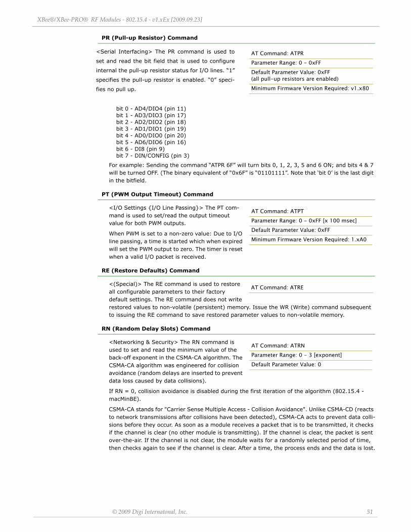
XBee®/XBee‐PRO® RF Modules ‐ 802.15.4 ‐ v1.xEx [2009.09.23]
© 2009 Digi Internatonal, Inc. 51
PR (Pull-up Resistor) Command
bit 0 - AD4/DIO4 (pin 11) bit 1 - AD3/DIO3 (pin 17) bit 2 - AD2/DIO2 (pin 18) bit 3 - AD1/DIO1 (pin 19) bit 4 - AD0/DIO0 (pin 20) bit 5 - AD6/DIO6 (pin 16) bit 6 - DI8 (pin 9) bit 7 - DIN/CONFIG (pin 3)
For example: Sending the command “ATPR 6F” will turn bits 0, 1, 2, 3, 5 and 6 ON; and bits 4 & 7 will be turned OFF. (The binary equivalent of “0x6F” is “01101111”. Note that ‘bit 0’ is the last digit in the bitfield.
PT (PWM Output Timeout) Command
<I/O Settings I/O Line Passing> The PT com-mand is used to set/read the output timeout value for both PWM outputs.
When PWM is set to a non-zero value: Due to I/O line passing, a time is started which when expired will set the PWM output to zero. The timer is reset when a valid I/O packet is received.
RE (Restore Defaults) Command
<(Special)> The RE command is used to restore all configurable parameters to their factory default settings. The RE command does not write restored values to non-volatile (persistent) memory. Issue the WR (Write) command subsequent to issuing the RE command to save restored parameter values to non-volatile memory.
RN (Random Delay Slots) Command
<Networking & Security> The RN command is used to set and read the minimum value of the back-off exponent in the CSMA-CA algorithm. The CSMA-CA algorithm was engineered for collision avoidance (random delays are inserted to prevent data loss caused by data collisions).
If RN = 0, collision avoidance is disabled during the first iteration of the algorithm (802.15.4 - macMinBE).
CSMA-CA stands for "Carrier Sense Multiple Access - Collision Avoidance". Unlike CSMA-CD (reacts to network transmissions after collisions have been detected), CSMA-CA acts to prevent data colli-sions before they occur. As soon as a module receives a packet that is to be transmitted, it checks if the channel is clear (no other module is transmitting). If the channel is clear, the packet is sent over-the-air. If the channel is not clear, the module waits for a randomly selected period of time, then checks again to see if the channel is clear. After a time, the process ends and the data is lost.
AT Command: ATPRParameter Range: 0 - 0xFFDefault Parameter Value: 0xFF (all pull-up resistors are enabled)Minimum Firmware Version Required: v1.x80
AT Command: ATPTParameter Range: 0 - 0xFF [x 100 msec]Default Parameter Value: 0xFFMinimum Firmware Version Required: 1.xA0
AT Command: ATRE
AT Command: ATRNParameter Range: 0 - 3 [exponent]Default Parameter Value: 0
<Serial Interfacing> The PR command is used to
set and read the bit field that is used to configure
internal the pull-up resistor status for I/O lines. “1”
specifies the pull-up resistor is enabled. “0” speci-
fies no pull up.
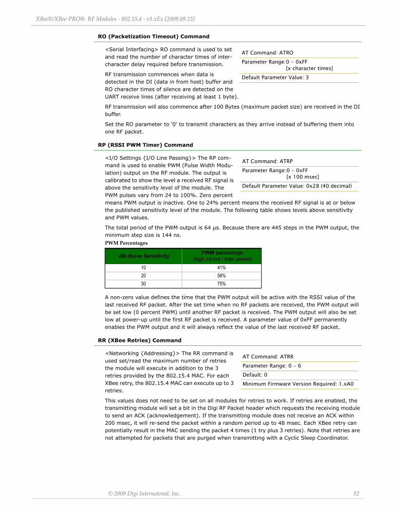
XBee®/XBee‐PRO® RF Modules ‐ 802.15.4 ‐ v1.xEx [2009.09.23]
© 2009 Digi Internatonal, Inc. 52
RO (Packetization Timeout) Command
<Serial Interfacing> RO command is used to set and read the number of character times of inter-character delay required before transmission.
RF transmission commences when data is detected in the DI (data in from host) buffer and RO character times of silence are detected on the UART receive lines (after receiving at least 1 byte).
RF transmission will also commence after 100 Bytes (maximum packet size) are received in the DI buffer.
Set the RO parameter to '0' to transmit characters as they arrive instead of buffering them into one RF packet.
RP (RSSI PWM Timer) Command
<I/O Settings I/O Line Passing> The RP com-mand is used to enable PWM (Pulse Width Modu-lation) output on the RF module. The output is calibrated to show the level a received RF signal is above the sensitivity level of the module. The PWM pulses vary from 24 to 100%. Zero percent means PWM output is inactive. One to 24% percent means the received RF signal is at or below the published sensitivity level of the module. The following table shows levels above sensitivity and PWM values.
The total period of the PWM output is 64 µs. Because there are 445 steps in the PWM output, the minimum step size is 144 ns.
A non-zero value defines the time that the PWM output will be active with the RSSI value of the last received RF packet. After the set time when no RF packets are received, the PWM output will be set low (0 percent PWM) until another RF packet is received. The PWM output will also be set low at power-up until the first RF packet is received. A parameter value of 0xFF permanently enables the PWM output and it will always reflect the value of the last received RF packet.
RR (XBee Retries) Command
<Networking Addressing> The RR command is used set/read the maximum number of retries the module will execute in addition to the 3 retries provided by the 802.15.4 MAC. For each XBee retry, the 802.15.4 MAC can execute up to 3 retries.
This values does not need to be set on all modules for retries to work. If retries are enabled, the transmitting module will set a bit in the Digi RF Packet header which requests the receiving module to send an ACK (acknowledgement). If the transmitting module does not receive an ACK within 200 msec, it will re-send the packet within a random period up to 48 msec. Each XBee retry can potentially result in the MAC sending the packet 4 times (1 try plus 3 retries). Note that retries are not attempted for packets that are purged when transmitting with a Cyclic Sleep Coordinator.
PWM Percentages
dB above Sensitivity PWM percentage(high period / total period)
10 41%20 58%30 75%
AT Command: ATROParameter Range:0 - 0xFF
[x character times]Default Parameter Value: 3
AT Command: ATRPParameter Range:0 - 0xFF
[x 100 msec]Default Parameter Value: 0x28 (40 decimal)
AT Command: ATRRParameter Range: 0 - 6Default: 0Minimum Firmware Version Required: 1.xA0
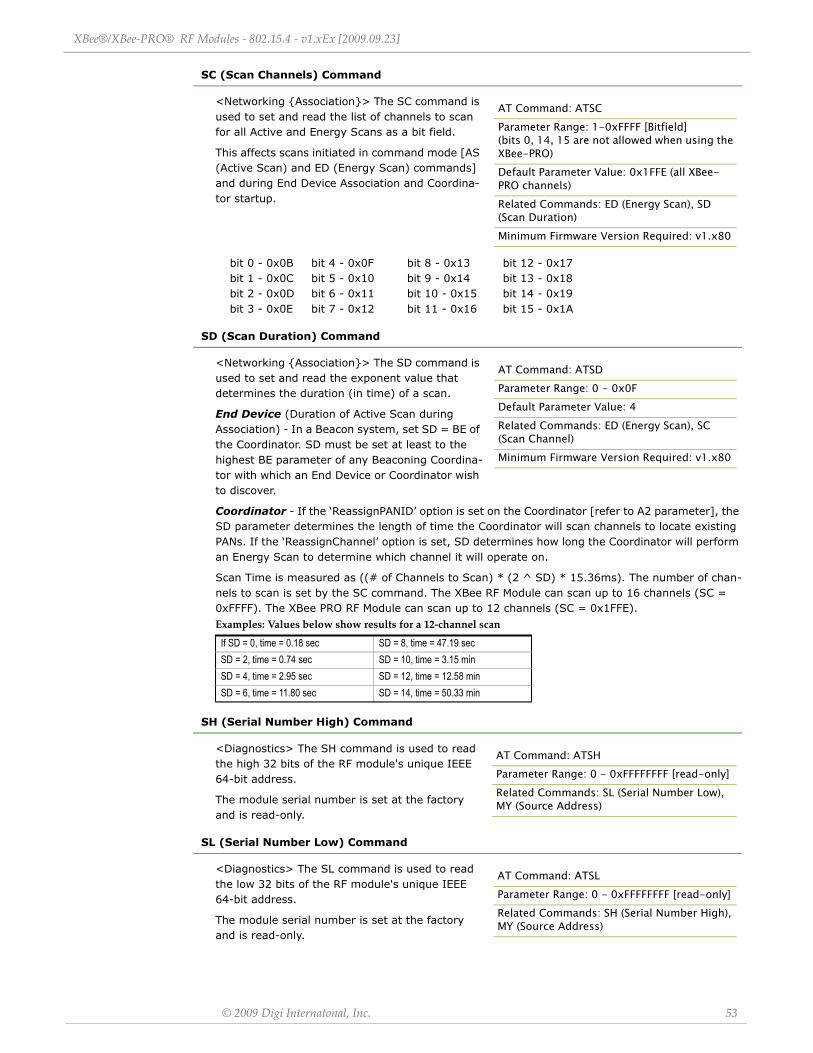
XBee®/XBee‐PRO® RF Modules ‐ 802.15.4 ‐ v1.xEx [2009.09.23]
© 2009 Digi Internatonal, Inc. 53
SC (Scan Channels) Command
<Networking Association> The SC command is used to set and read the list of channels to scan for all Active and Energy Scans as a bit field.
This affects scans initiated in command mode [AS (Active Scan) and ED (Energy Scan) commands] and during End Device Association and Coordina-tor startup.
bit 0 - 0x0B bit 4 - 0x0F bit 8 - 0x13 bit 12 - 0x17 bit 1 - 0x0C bit 5 - 0x10 bit 9 - 0x14 bit 13 - 0x18 bit 2 - 0x0D bit 6 - 0x11 bit 10 - 0x15 bit 14 - 0x19 bit 3 - 0x0E bit 7 - 0x12 bit 11 - 0x16 bit 15 - 0x1A
SD (Scan Duration) Command
<Networking Association> The SD command is used to set and read the exponent value that determines the duration (in time) of a scan.
End Device (Duration of Active Scan during Association) - In a Beacon system, set SD = BE of the Coordinator. SD must be set at least to the highest BE parameter of any Beaconing Coordina-tor with which an End Device or Coordinator wish to discover.
Coordinator - If the ‘ReassignPANID’ option is set on the Coordinator [refer to A2 parameter], the SD parameter determines the length of time the Coordinator will scan channels to locate existing PANs. If the ‘ReassignChannel’ option is set, SD determines how long the Coordinator will perform an Energy Scan to determine which channel it will operate on.
Scan Time is measured as ((# of Channels to Scan) * (2 ^ SD) * 15.36ms). The number of chan-nels to scan is set by the SC command. The XBee RF Module can scan up to 16 channels (SC = 0xFFFF). The XBee PRO RF Module can scan up to 12 channels (SC = 0x1FFE).
SH (Serial Number High) Command
<Diagnostics> The SH command is used to read the high 32 bits of the RF module's unique IEEE 64-bit address.
The module serial number is set at the factory and is read-only.
SL (Serial Number Low) Command
<Diagnostics> The SL command is used to read the low 32 bits of the RF module's unique IEEE 64-bit address.
The module serial number is set at the factory and is read-only.
Examples: Values below show results for a 12‐channel scan
If SD = 0, time = 0.18 sec SD = 8, time = 47.19 secSD = 2, time = 0.74 sec SD = 10, time = 3.15 minSD = 4, time = 2.95 sec SD = 12, time = 12.58 minSD = 6, time = 11.80 sec SD = 14, time = 50.33 min
AT Command: ATSCParameter Range: 1-0xFFFF [Bitfield] (bits 0, 14, 15 are not allowed when using the XBee-PRO)Default Parameter Value: 0x1FFE (all XBee-PRO channels)Related Commands: ED (Energy Scan), SD (Scan Duration)Minimum Firmware Version Required: v1.x80
AT Command: ATSDParameter Range: 0 - 0x0FDefault Parameter Value: 4Related Commands: ED (Energy Scan), SC (Scan Channel)Minimum Firmware Version Required: v1.x80
AT Command: ATSHParameter Range: 0 - 0xFFFFFFFF [read-only]Related Commands: SL (Serial Number Low), MY (Source Address)
AT Command: ATSLParameter Range: 0 - 0xFFFFFFFF [read-only]Related Commands: SH (Serial Number High), MY (Source Address)
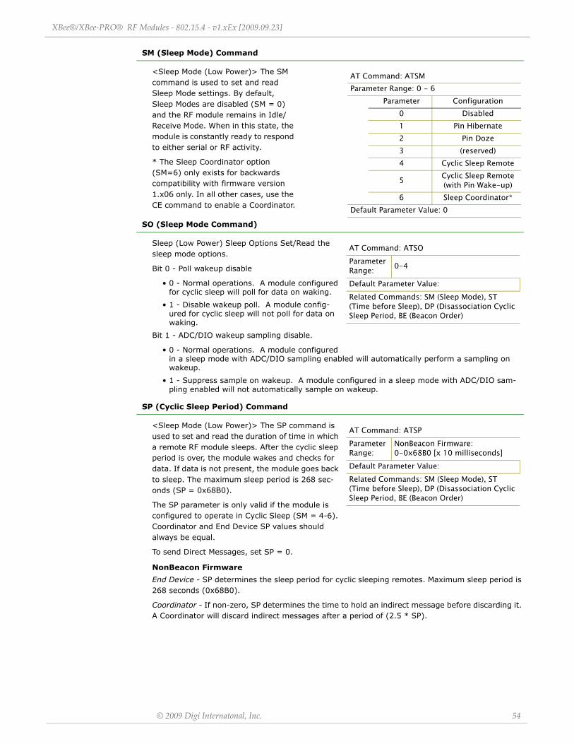
XBee®/XBee‐PRO® RF Modules ‐ 802.15.4 ‐ v1.xEx [2009.09.23]
© 2009 Digi Internatonal, Inc. 54
SM (Sleep Mode) Command
<Sleep Mode (Low Power)> The SM command is used to set and read Sleep Mode settings. By default, Sleep Modes are disabled (SM = 0) and the RF module remains in Idle/Receive Mode. When in this state, the module is constantly ready to respond to either serial or RF activity.
* The Sleep Coordinator option (SM=6) only exists for backwards compatibility with firmware version 1.x06 only. In all other cases, use the CE command to enable a Coordinator.
SO (Sleep Mode Command)
Sleep (Low Power) Sleep Options Set/Read the sleep mode options.
Bit 0 - Poll wakeup disable
• 0 - Normal operations. A module configured for cyclic sleep will poll for data on waking.
• 1 - Disable wakeup poll. A module config-ured for cyclic sleep will not poll for data on waking.
Bit 1 - ADC/DIO wakeup sampling disable.
• 0 - Normal operations. A module configured in a sleep mode with ADC/DIO sampling enabled will automatically perform a sampling on wakeup.
• 1 - Suppress sample on wakeup. A module configured in a sleep mode with ADC/DIO sam-pling enabled will not automatically sample on wakeup.
SP (Cyclic Sleep Period) Command
<Sleep Mode (Low Power)> The SP command is used to set and read the duration of time in which a remote RF module sleeps. After the cyclic sleep period is over, the module wakes and checks for data. If data is not present, the module goes back to sleep. The maximum sleep period is 268 sec-onds (SP = 0x68B0).
The SP parameter is only valid if the module is configured to operate in Cyclic Sleep (SM = 4-6). Coordinator and End Device SP values should always be equal.
To send Direct Messages, set SP = 0.
NonBeacon Firmware
End Device - SP determines the sleep period for cyclic sleeping remotes. Maximum sleep period is 268 seconds (0x68B0).
Coordinator - If non-zero, SP determines the time to hold an indirect message before discarding it. A Coordinator will discard indirect messages after a period of (2.5 * SP).
AT Command: ATSMParameter Range: 0 - 6 Parameter Configuration
0 Disabled1 Pin Hibernate2 Pin Doze3 (reserved)4 Cyclic Sleep Remote
5 Cyclic Sleep Remote(with Pin Wake-up)
6 Sleep Coordinator*Default Parameter Value: 0
AT Command: ATSOParameter Range: 0-4
Default Parameter Value:Related Commands: SM (Sleep Mode), ST (Time before Sleep), DP (Disassociation Cyclic Sleep Period, BE (Beacon Order)
AT Command: ATSPParameter Range:
NonBeacon Firmware: 0-0x68B0 [x 10 milliseconds]
Default Parameter Value:Related Commands: SM (Sleep Mode), ST (Time before Sleep), DP (Disassociation Cyclic Sleep Period, BE (Beacon Order)

XBee®/XBee‐PRO® RF Modules ‐ 802.15.4 ‐ v1.xEx [2009.09.23]
© 2009 Digi Internatonal, Inc. 55
ST (Time before Sleep) Command
<Sleep Mode (Low Power)> The ST command is used to set and read the period of inactivity (no serial or RF data is sent or received) before acti-vating Sleep Mode.
NonBeacon Firmware
Set/Read time period of inactivity (no serial or RF data is sent or received) before activating Sleep Mode. ST parameter is only valid with Cyclic Sleep settings (SM = 4 - 5).
Coordinator and End Device ST values must be equal.
AT Command: ATSTParameter Range:
NonBeacon Firmware: 1 - 0xFFFF [x 1 millisecond]
Default Parameter Value:Related Commands: SM (Sleep Mode), ST (Time before Sleep)
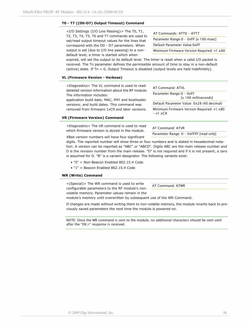
XBee®/XBee‐PRO® RF Modules ‐ 802.15.4 ‐ v1.xEx [2009.09.23]
© 2009 Digi Internatonal, Inc. 56
T0 - T7 ((D0-D7) Output Timeout) Command
<I/O Settings I/O Line Passing> The T0, T1, T2, T3, T4, T5, T6 and T7 commands are used to set/read output timeout values for the lines that correspond with the D0 - D7 parameters. When output is set (due to I/O line passing) to a non-default level, a timer is started which when expired, will set the output to its default level. The timer is reset when a valid I/O packet is received. The Tn parameter defines the permissible amount of time to stay in a non-default (active) state. If Tn = 0, Output Timeout is disabled (output levels are held indefinitely).
VL (Firmware Version - Verbose)
<Diagnostics> The VL command is used to read detailed version information about the RF module. The information includes: application build date; MAC, PHY and bootloader versions; and build dates. This command was removed from firmware 1xC9 and later versions.
VR (Firmware Version) Command
<Diagnostics> The VR command is used to read which firmware version is stored in the module.
XBee version numbers will have four significant digits. The reported number will show three or four numbers and is stated in hexadecimal nota-tion. A version can be reported as "ABC" or "ABCD". Digits ABC are the main release number and D is the revision number from the main release. "D" is not required and if it is not present, a zero is assumed for D. "B" is a variant designator. The following variants exist:
• "0" = Non-Beacon Enabled 802.15.4 Code
• "1" = Beacon Enabled 802.15.4 Code
WR (Write) Command
<(Special)> The WR command is used to write configurable parameters to the RF module's non-volatile memory. Parameter values remain in the module's memory until overwritten by subsequent use of the WR Command.
If changes are made without writing them to non-volatile memory, the module reverts back to pre-viously saved parameters the next time the module is powered-on.
NOTE: Once the WR command is sent to the module, no additional characters should be sent until after the “OK/r” response is received.
AT Commands: ATT0 - ATT7Parameter Range:0 - 0xFF [x 100 msec]Default Parameter Value:0xFFMinimum Firmware Version Required: v1.xA0
AT Command: ATVLParameter Range:0 - 0xFF
[x 100 milliseconds]Default Parameter Value: 0x28 (40 decimal)Minimum Firmware Version Required: v1.x80 - v1.xC8
AT Command: ATVRParameter Range: 0 - 0xFFFF [read only]
AT Command: ATWR
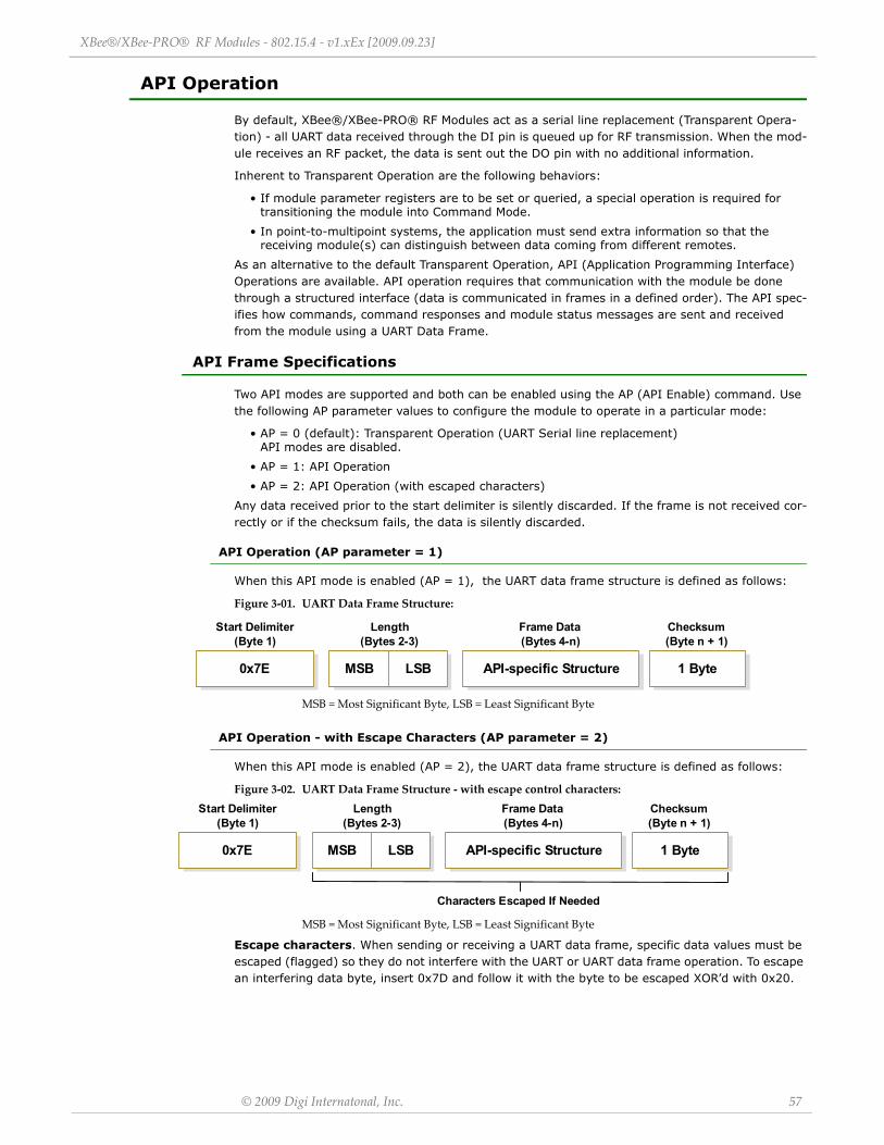
XBee®/XBee‐PRO® RF Modules ‐ 802.15.4 ‐ v1.xEx [2009.09.23]
© 2009 Digi Internatonal, Inc. 57
API Operation
By default, XBee®/XBee-PRO® RF Modules act as a serial line replacement (Transparent Opera-tion) - all UART data received through the DI pin is queued up for RF transmission. When the mod-ule receives an RF packet, the data is sent out the DO pin with no additional information.
Inherent to Transparent Operation are the following behaviors:
• If module parameter registers are to be set or queried, a special operation is required for transitioning the module into Command Mode.
• In point-to-multipoint systems, the application must send extra information so that the receiving module(s) can distinguish between data coming from different remotes.
As an alternative to the default Transparent Operation, API (Application Programming Interface) Operations are available. API operation requires that communication with the module be done through a structured interface (data is communicated in frames in a defined order). The API spec-ifies how commands, command responses and module status messages are sent and received from the module using a UART Data Frame.
API Frame Specifications
Two API modes are supported and both can be enabled using the AP (API Enable) command. Use the following AP parameter values to configure the module to operate in a particular mode:
• AP = 0 (default): Transparent Operation (UART Serial line replacement) API modes are disabled.
• AP = 1: API Operation
• AP = 2: API Operation (with escaped characters)
Any data received prior to the start delimiter is silently discarded. If the frame is not received cor-rectly or if the checksum fails, the data is silently discarded.
API Operation (AP parameter = 1)
When this API mode is enabled (AP = 1), the UART data frame structure is defined as follows:
Figure 3‐01. UART Data Frame Structure:
MSB = Most Significant Byte, LSB = Least Significant Byte
API Operation - with Escape Characters (AP parameter = 2)
When this API mode is enabled (AP = 2), the UART data frame structure is defined as follows:
Figure 3‐02. UART Data Frame Structure ‐ with escape control characters:
MSB = Most Significant Byte, LSB = Least Significant Byte
Escape characters. When sending or receiving a UART data frame, specific data values must be escaped (flagged) so they do not interfere with the UART or UART data frame operation. To escape an interfering data byte, insert 0x7D and follow it with the byte to be escaped XOR’d with 0x20.
Start Delimiter(Byte 1)
Length(Bytes 2-3)
Frame Data(Bytes 4-n)
Checksum(Byte n + 1)
0x7E MSB LSB API-specific Structure 1 Byte
Start Delimiter(Byte 1)
Length(Bytes 2-3)
Frame Data(Bytes 4-n)
Checksum(Byte n + 1)
0x7E MSB LSB API-specific Structure 1 Byte
Characters Escaped If Needed
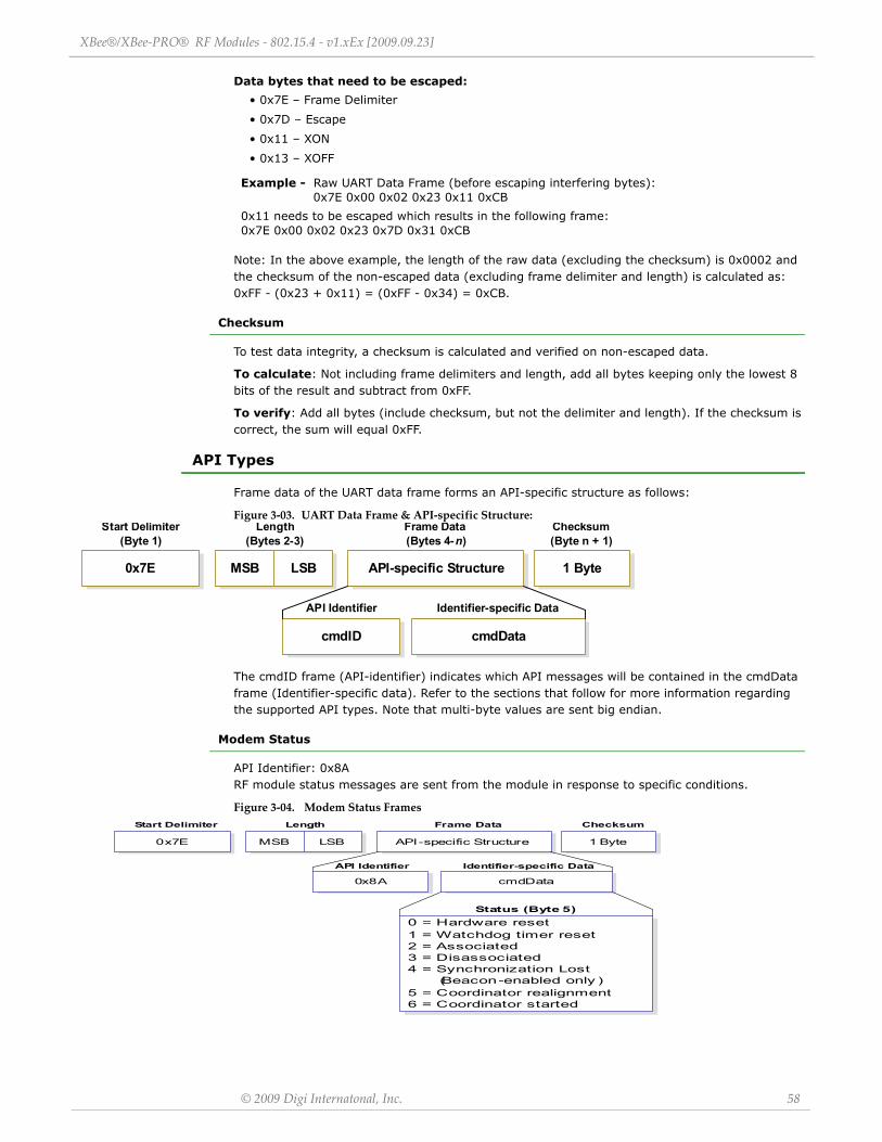
XBee®/XBee‐PRO® RF Modules ‐ 802.15.4 ‐ v1.xEx [2009.09.23]
© 2009 Digi Internatonal, Inc. 58
Data bytes that need to be escaped:
• 0x7E – Frame Delimiter
• 0x7D – Escape
• 0x11 – XON
• 0x13 – XOFF
Note: In the above example, the length of the raw data (excluding the checksum) is 0x0002 and the checksum of the non-escaped data (excluding frame delimiter and length) is calculated as: 0xFF - (0x23 + 0x11) = (0xFF - 0x34) = 0xCB.
Checksum
To test data integrity, a checksum is calculated and verified on non-escaped data.
To calculate: Not including frame delimiters and length, add all bytes keeping only the lowest 8 bits of the result and subtract from 0xFF.
To verify: Add all bytes (include checksum, but not the delimiter and length). If the checksum is correct, the sum will equal 0xFF.
API Types
Frame data of the UART data frame forms an API-specific structure as follows:
Figure 3‐03. UART Data Frame & API‐specific Structure:
The cmdID frame (API-identifier) indicates which API messages will be contained in the cmdData frame (Identifier-specific data). Refer to the sections that follow for more information regarding the supported API types. Note that multi-byte values are sent big endian.
Modem Status
API Identifier: 0x8A RF module status messages are sent from the module in response to specific conditions.
Figure 3‐04. Modem Status Frames
Example - Raw UART Data Frame (before escaping interfering bytes): 0x7E 0x00 0x02 0x23 0x11 0xCB
0x11 needs to be escaped which results in the following frame: 0x7E 0x00 0x02 0x23 0x7D 0x31 0xCB
Length(Bytes 2-3)
Checksum(Byte n + 1)
MSB LSB 1 Byte
Start Delimiter(Byte 1)
0x7E
Frame Data(Bytes 4-n)
API-specific Structure
Identifier-specific Data
cmdData
API Identifier
cmdID
cmdData0x8A
Length ChecksumStart Delimiter Frame Data
Identifier-specific DataAPI Identifier
MSB LSB0x7E 1 ByteAPI-specific Structure
Status (Byte 5)0 = Hardware reset1 = Watchdog timer reset2 = Associated3 = Disassociated4 = Synchronization Lost (Beacon-enabled only )5 = Coordinator realignment6 = Coordinator started
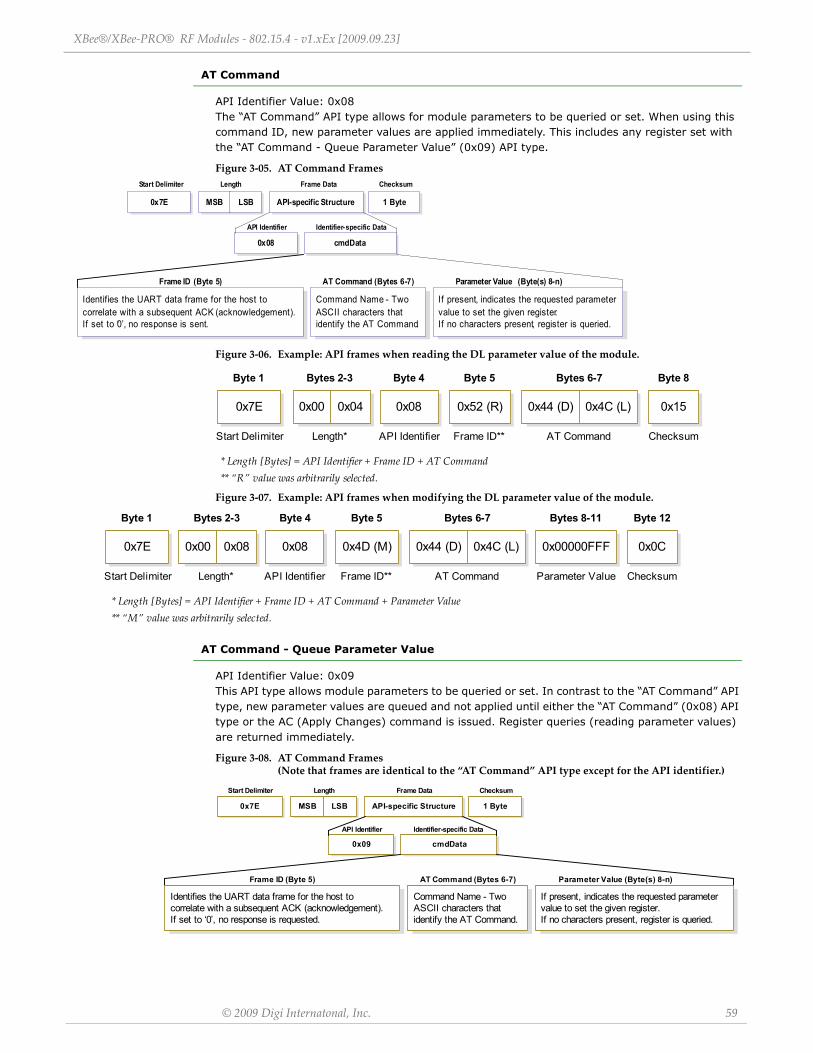
XBee®/XBee‐PRO® RF Modules ‐ 802.15.4 ‐ v1.xEx [2009.09.23]
© 2009 Digi Internatonal, Inc. 59
AT Command
API Identifier Value: 0x08 The “AT Command” API type allows for module parameters to be queried or set. When using this command ID, new parameter values are applied immediately. This includes any register set with the “AT Command - Queue Parameter Value” (0x09) API type.
Figure 3‐05. AT Command Frames
Figure 3‐06. Example: API frames when reading the DL parameter value of the module.
Figure 3‐07. Example: API frames when modifying the DL parameter value of the module.
AT Command - Queue Parameter Value
API Identifier Value: 0x09 This API type allows module parameters to be queried or set. In contrast to the “AT Command” API type, new parameter values are queued and not applied until either the “AT Command” (0x08) API type or the AC (Apply Changes) command is issued. Register queries (reading parameter values) are returned immediately.
Figure 3‐08. AT Command Frames (Note that frames are identical to the “AT Command” API type except for the API identifier.)
cmdData0x08
Length ChecksumStart Delimiter Frame Data
Identifier-specific DataAPI Identifier
MSB LSB0x7E 1 ByteAPI-specific Structure
Frame ID (Byte 5)
Identifies the UART data frame for the host to correlate with a subsequent ACK (acknowledgement).If set to ‘0’, no response is sent.
AT Command (Bytes 6-7)
Command Name - Two ASCII characters that identify the AT Command.
Parameter Value (Byte(s) 8-n)
If present, indicates the requested parameter value to set the given register.If no characters present, register is queried.
* Length [Bytes] = API Identifier + Frame ID + AT Command** “R” value was arbitrarily selected.
Checksum
0x15
Byte 8
AT Command
Bytes 6-7
Frame ID**
0x52 (R)
Byte 5
0x44 (D) 0x4C (L)
API Identifier
0x08
Byte 4
Start Delimiter
Byte 1
0x7E
Length*
Bytes 2-3
0x00 0x04
* Length [Bytes] = API Identifier + Frame ID + AT Command + Parameter Value** “M” value was arbitrarily selected.
Checksum
0x0C
Byte 12
AT Command
Bytes 6-7
0x44 (D) 0x4C (L)
Parameter Value
0x00000FFF
Bytes 8-11
Frame ID**
0x4D (M)
Byte 5
Length*
Bytes 2-3
0x00 0x08
API Identifier
0x08
Byte 4
Start Delimiter
Byte 1
0x7E
cmdData0x09
Length ChecksumStart Delimiter Frame Data
Identifier-specific DataAPI Identifier
MSB LSB0x7E 1 ByteAPI-specific Structure
Frame ID (Byte 5)
Identifies the UART data frame for the host tocorrelate with a subsequent ACK (acknowledgement).If set to ‘0’, no response is requested.
AT Command (Bytes 6-7)
Command Name - TwoASCII characters thatidentify the AT Command.
Parameter Value (Byte(s) 8-n)
If present, indicates the requested parametervalue to set the given register.If no characters present, register is queried.
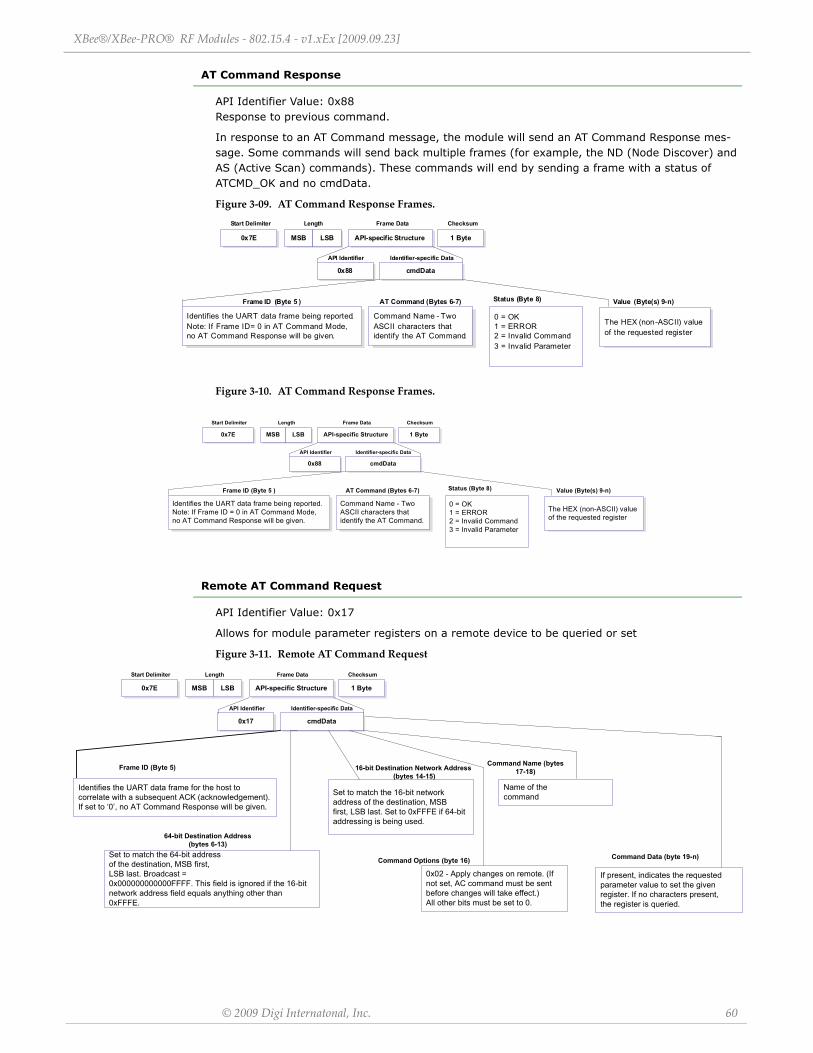
XBee®/XBee‐PRO® RF Modules ‐ 802.15.4 ‐ v1.xEx [2009.09.23]
© 2009 Digi Internatonal, Inc. 60
AT Command Response
API Identifier Value: 0x88 Response to previous command.
In response to an AT Command message, the module will send an AT Command Response mes-sage. Some commands will send back multiple frames (for example, the ND (Node Discover) and AS (Active Scan) commands). These commands will end by sending a frame with a status of ATCMD_OK and no cmdData.
Figure 3‐09. AT Command Response Frames.
Figure 3‐10. AT Command Response Frames.
Remote AT Command Request
API Identifier Value: 0x17
Allows for module parameter registers on a remote device to be queried or set
Figure 3‐11. Remote AT Command Request
cmdData0x88
Length ChecksumStart Delimiter Frame Data
Identifier-specific DataAPI Identifier
MSB LSB0x7E 1 ByteAPI-specific Structure
Frame ID (Byte 5 )
Identifies the UART data frame being reported.Note: If Frame ID = 0 in AT Command Mode, no AT Command Response will be given.
AT Command (Bytes 6-7)
Command Name - Two ASCII characters that identify the AT Command.
Status (Byte 8)
0 = OK1 = ERROR2 = Invalid Command3 = Invalid Parameter
The HEX (non-ASCII) value of the requested register
Value (Byte(s) 9-n)
0x17 cmdData
Length ChecksumStart Delimiter Frame Data
Identifier-specific DataAPI Identifier
MSB LSB0x7E 1 ByteAPI-specific Structure
Frame ID (Byte 5)
Identifies the UART data frame for the host to correlate with a subsequent ACK (acknowledgement).If set to ‘0’, no AT Command Response will be given.
Command Name (bytes17-18)
Name of thecommand
Set to match the 64-bit addressof the destination, MSB first,LSB last. Broadcast =0x000000000000FFFF. This field is ignored if the 16-bit network address field equals anything other than 0xFFFE.
64-bit Destination Address(bytes 6-13)
0x02 - Apply changes on remote. (Ifnot set, AC command must be sentbefore changes will take effect.)All other bits must be set to 0.
Command Options (byte 16)
If present, indicates the requestedparameter value to set the givenregister. If no characters present,the register is queried.
Command Data (byte 19-n)
16-bit Destination Network Address (bytes 14-15)
Set to match the 16-bit networkaddress of the destination, MSBfirst, LSB last. Set to 0xFFFE if 64-bit addressing is being used.
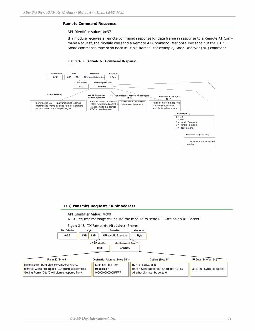
XBee®/XBee‐PRO® RF Modules ‐ 802.15.4 ‐ v1.xEx [2009.09.23]
© 2009 Digi Internatonal, Inc. 61
Remote Command Response
API Identifier Value: 0x97
If a module receives a remote command response RF data frame in response to a Remote AT Com-mand Request, the module will send a Remote AT Command Response message out the UART. Some commands may send back multiple frames--for example, Node Discover (ND) command.
Figure 3‐12. Remote AT Command Response.
TX (Transmit) Request: 64-bit address
API Identifier Value: 0x00 A TX Request message will cause the module to send RF Data as an RF Packet.
Figure 3‐13. TX Packet (64‐bit address) Frames
cmdData0x97
Length ChecksumStart Delimiter Frame Data
Identifier- specific DataAPI Identifier
MSB LSB0x7E 1 ByteAPI- specific Structure
16- bit Responder Network Address ( bytes 14-15)
Set to the 16- bit network address of the remote.
.
Frame ID ( Byte 5)
Status ( byte 18)
0 = OK1 = Error2 = Invalid Command3 = Invalid Parameter
64- bit Responder Address ( bytes 6-13)
Indicates the 64- bit address of the remote module that is responding to the Remote
AT Command request
Identifies the UART data frame being reported. Matches the Frame ID of the Remote Command
Request the remote is responding to.
Command Name ( bytes 16-17)
Name of the command. Two ASCII characters that identify the AT command
Command Data ( byte 19-n)
The value of the requested register.
4 = No Response
cmdData0x00
Length ChecksumStart Delimiter Frame Data
Identifier-specific DataAPI Identifier
MSB LSB0x7E 1 ByteAPI-specific Structure
Frame ID (Byte 5)
Identifies the UART data frame for the host tocorrelate with a subsequent ACK (acknowledgement).Setting Frame ID to ‘0' will disable response frame.
Destination Address (Bytes 6-13)
MSB first, LSB last.Broadcast =0x000000000000FFFF
Options (Byte 14)
0x01 = Disable ACK0x04 = Send packet with Broadcast Pan IDAll other bits must be set to 0.
RF Data (Byte(s) 15-n)
Up to 100 Bytes per packet
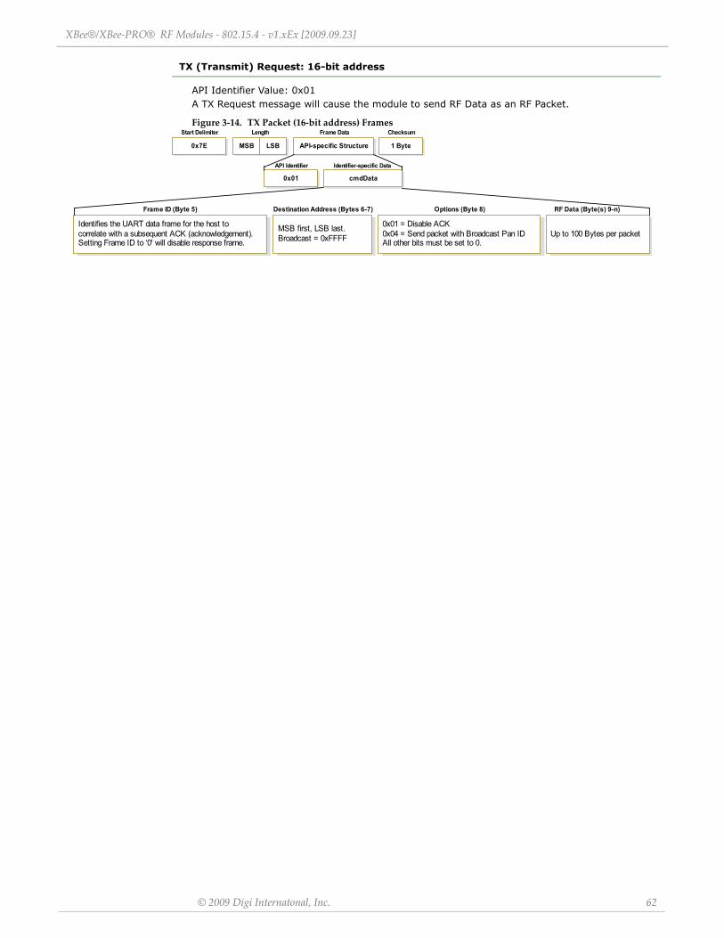
XBee®/XBee‐PRO® RF Modules ‐ 802.15.4 ‐ v1.xEx [2009.09.23]
© 2009 Digi Internatonal, Inc. 62
TX (Transmit) Request: 16-bit address
API Identifier Value: 0x01 A TX Request message will cause the module to send RF Data as an RF Packet.
Figure 3‐14. TX Packet (16‐bit address) Frames
cmdData0x01
Length ChecksumStart Delimiter Frame Data
Identifier-specific DataAPI Identifier
MSB LSB0x7E 1 ByteAPI-specific Structure
Frame ID (Byte 5)
Identifies the UART data frame for the host tocorrelate with a subsequent ACK (acknowledgement).Setting Frame ID to ‘0' will disable response frame.
Destination Address (Bytes 6-7)
MSB first, LSB last.Broadcast = 0xFFFF
Options (Byte 8)
0x01 = Disable ACK0x04 = Send packet with Broadcast Pan IDAll other bits must be set to 0.
RF Data (Byte(s) 9-n)
Up to 100 Bytes per packet
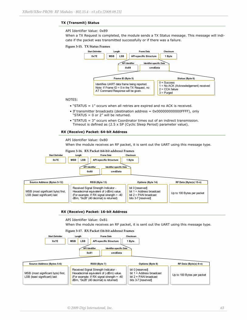
XBee®/XBee‐PRO® RF Modules ‐ 802.15.4 ‐ v1.xEx [2009.09.23]
© 2009 Digi Internatonal, Inc. 63
TX (Transmit) Status
API Identifier Value: 0x89 When a TX Request is completed, the module sends a TX Status message. This message will indi-cate if the packet was transmitted successfully or if there was a failure.
Figure 3‐15. TX Status Frames
NOTES:
• “STATUS = 1” occurs when all retries are expired and no ACK is received.
• If transmitter broadcasts (destination address = 0x000000000000FFFF), only “STATUS = 0 or 2” will be returned.
• “STATUS = 3” occurs when Coordinator times out of an indirect transmission. Timeout is defined as (2.5 x SP (Cyclic Sleep Period) parameter value).
RX (Receive) Packet: 64-bit Address
API Identifier Value: 0x80 When the module receives an RF packet, it is sent out the UART using this message type.
Figure 3‐16. RX Packet (64‐bit address) Frames
RX (Receive) Packet: 16-bit Address
API Identifier Value: 0x81 When the module receives an RF packet, it is sent out the UART using this message type.
Figure 3‐17. RX Packet (16‐bit address) Frames
cmdData0x89
Length ChecksumStart Delimiter Frame Data
Identifier-specific DataAPI Identifier
MSB LSB0x7E 1 ByteAPI-specific Structure
Frame ID (Byte 5) Status (Byte 6)
0 = Success1 = No ACK (Acknowledgement) received2 = CCA failure3 = Purged
Identifies UART data frame being reported.Note: If Frame ID = 0 in the TX Request, noAT Command Response will be given.
cmdData0x80
Length ChecksumStart Delimiter Frame Data
Identifier-specific DataAPI Identifier
MSB LSB0x7E 1 ByteAPI-specific Structure
bit 0 [reserved]bit 1 = Address broadcastbit 2 = PAN broadcastbits 3-7 [reserved]
Up to 100 Bytes per packet
Received Signal Strength Indicator -Hexadecimal equivalent of (-dBm) value.(For example: If RX signal strength = -40dBm, “0x28” (40 decimal) is returned)
Source Address (Bytes 5-12) Options (Byte 14) RF Data (Byte(s) 15-n)RSSI (Byte 13)
MSB (most significant byte) first,LSB (least significant) last
cmdData0x81
Length ChecksumStart Delimiter Frame Data
Identifier-specific DataAPI Identifier
MSB LSB0x7E 1 ByteAPI-specific Structure
bit 0 [reserved]bit 1 = Address broadcastbit 2 = PAN broadcastbits 3-7 [reserved]
Up to 100 Bytes per packet
Received Signal Strength Indicator -Hexadecimal equivalent of (-dBm) value.(For example: If RX signal strength = -40dBm, “0x28” (40 decimal) is returned)
Source Address (Bytes 5-6) RSSI (Byte 7)
MSB (most significant byte) first,LSB (least significant) last
Options (Byte 8) RF Data (Byte(s) 9-n)

© 2009 Digi International Inc. 64
Appendix A: Agency Certifications
United States (FCC)
XBee®/XBee-PRO® RF Modules comply with Part 15 of the FCC rules and regulations. Compliance with the labeling requirements, FCC notices and antenna usage guidelines is required.
To fulfill FCC Certification requirements, the OEM must comply with the following regulations:
OEM Labeling Requirements
WARNING: The Original Equipment Manufacturer (OEM) must ensure that FCC labeling requirements are met. This includes a clearly visible label on the outside of the final product enclosure that displays the contents shown in the figure below.
Figure 4‐01. Required FCC Label for OEM products containing the XBee®/XBee‐PRO® RF Module
* The FCC ID for the XBee is “OUR‐XBEE”. The FCC ID for the XBee‐PRO is “OUR‐XBEEPRO”.
FCC Notices
IMPORTANT: The XBee®/XBee-PRO® RF Module has been certified by the FCC for use with other products without any further certification (as per FCC section 2.1091). Modifications not expressly approved by Digi could void the user's authority to operate the equipment.
IMPORTANT: OEMs must test final product to comply with unintentional radiators (FCC section 15.107 & 15.109) before declaring compliance of their final product to Part 15 of the FCC Rules.
IMPORTANT: The RF module has been certified for remote and base radio applications. If the module will be used for portable applications, the device must undergo SAR testing.
This equipment has been tested and found to comply with the limits for a Class B digital device, pursuant to Part 15 of the FCC Rules. These limits are designed to provide reasonable protection against harmful interference in a residential installation. This equipment generates, uses and can radiate radio frequency energy and, if not installed and used in accordance with the instructions, may cause harmful interference to radio communications. However, there is no guarantee that interference will not occur in a particular installation.
If this equipment does cause harmful interference to radio or television reception, which can be determined by turning the equipment off and on, the user is encouraged to try to correct the inter-ference by one or more of the following measures: Re-orient or relocate the receiving antenna, Increase the separation between the equipment and receiver, Connect equipment and receiver to outlets on different circuits, or Consult the dealer or an experienced radio/TV technician for help.
1. The system integrator must ensure that the text on the external label provided with this device is placed on the outside of the final product [Figure A-01].
2. XBee®/XBee-PRO® RF Modules may only be used with antennas that have been tested and approved for use with this module [refer to the antenna tables in this section].
Contains FCC ID: OUR-XBEE/OUR-XBEEPRO**
The enclosed device complies with Part 15 of the FCC Rules. Operation is subject to the following two conditions: (i.) this device may not cause harmful interference and (ii.) this device must accept any inter-ference received, including interference that may cause undesired operation.
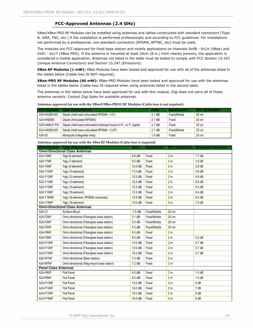
XBee®/XBee‐PRO® RF Modules ‐ 802.15.4 ‐ v1.xEx [2009.09.23]
© 2009 Digi Internatonal, Inc. 65
FCC-Approved Antennas (2.4 GHz)
XBee/XBee-PRO RF Modules can be installed using antennas and cables constructed with standard connectors (Type-N, SMA, TNC, etc.) if the installation is performed professionally and according to FCC guidelines. For installations not performed by a professional, non-standard connectors (RPSMA, RPTNC, etc) must be used.
The modules are FCC-approved for fixed base station and mobile applications on channels 0x0B - 0x1A (XBee) and 0x0C - 0x17 (XBee-PRO). If the antenna is mounted at least 20cm (8 in.) from nearby persons, the application is considered a mobile application. Antennas not listed in the table must be tested to comply with FCC Section 15.203 (Unique Antenna Connectors) and Section 15.247 (Emissions).
XBee RF Modules (1 mW): XBee Modules have been tested and approved for use with all of the antennas listed in the tables below (Cable-loss IS NOT required).
XBee-PRO RF Modules (60 mW): XBee-PRO Modules have been tested and approved for use with the antennas listed in the tables below (Cable-loss IS required when using antennas listed in the second table.
The antennas in the tables below have been approved for use with this module. Digi does not carry all of these antenna variants. Contact Digi Sales for available antennas.
Antennas approved for use with the XBee®/XBee‐PRO® RF Modules (Cable‐loss is not required.)
Antennas approved for use with the XBee RF Modules (Cable‐loss is required)
Part Number Type (Description) Gain Application* Min. SeparationA24-HASM-450 Dipole (Half-wave articulated RPSMA - 4.5”) 2.1 dBi Fixed/Mobile 20 cmA24-HABSM Dipole (Articulated RPSMA) 2.1 dBi Fixed 20 cmA24-HABUF-P5I Dipole (Half-wave articulated bulkhead mount U.FL. w/ 5” pigtail) 2.1 dBi Fixed 20 cmA24-HASM-525 Dipole (Half-wave articulated RPSMA - 5.25") 2.1 dBi Fixed/Mobile 20 cmA24-QI Monopole (Integrated whip) 1.5 dBi Fixed 20 cm
Part Number Type (Description) Gain Application* Min. Separation Required Cable-lossOmni-Directional Class AntennasA24-Y6NF Yagi (6-element) 8.8 dBi Fixed 2 m 1.7 dBA24-Y7NF Yagi (7-element) 9.0 dBi Fixed 2 m 1.9 dBA24-Y9NF Yagi (9-element) 10.0 dBi Fixed 2 m 2.9 dBA24-Y10NF Yagi (10-element) 11.0 dBi Fixed 2 m 3.9 dBA24-Y12NF Yagi (12-element) 12.0 dBi Fixed 2 m 4.9 dBA24-Y13NF Yagi (13-element) 12.0 dBi Fixed 2 m 4.9 dBA24-Y15NF Yagi (15-element) 12.5 dBi Fixed 2 m 5.4 dBA24-Y16NF Yagi (16-element) 13.5 dBi Fixed 2 m 6.4 dBA24-Y16RM Yagi (16-element, RPSMA connector) 13.5 dBi Fixed 2 m 6.4 dBA24-Y18NF Yagi (18-element) 15.0 dBi Fixed 2 m 7.9 dBOmni-Directional Class AntennasA24-C1 Surface Mount -1.5 dBi Fixed/Mobile 20 cm -A24-F2NF Omni-directional (Fiberglass base station) 2.1 dBi Fixed/Mobile 20 cmA24-F3NF Omni-directional (Fiberglass base station) 3.0 dBi Fixed/Mobile 20 cmA24-F5NF Omni-directional (Fiberglass base station) 5.0 dBi Fixed/Mobile 20 cmA24-F8NF Omni-directional (Fiberglass base station) 8.0 dBi Fixed 2 mA24-F9NF Omni-directional (Fiberglass base station) 9.5 dBi Fixed 2 m 0.2 dBA24-F10NF Omni-directional (Fiberglass base station) 10.0 dBi Fixed 2 m 0.7 dBA24-F12NF Omni-directional (Fiberglass base station) 12.0 dBi Fixed 2 m 2.7 dBA24-F15NF Omni-directional (Fiberglass base station) 15.0 dBi Fixed 2 m 5.7 dBA24-W7NF Omni-directional (Base station) 7.2 dBi Fixed 2 mA24-M7NF Omni-directional (Mag-mount base station) 7.2 dBi Fixed 2 mPanel Class AntennasA24-P8SF Flat Panel 8.5 dBi Fixed 2 m 1.5 dBA24-P8NF Flat Panel 8.5 dBi Fixed 2 m 1.5 dBA24-P13NF Flat Panel 13.0 dBi Fixed 2 m 6 dBA24-P14NF Flat Panel 14.0 dBi Fixed 2 m 7 dBA24-P15NF Flat Panel 15.0 dBi Fixed 2 m 8 dBA24-P16NF Flat Panel 16.0 dBi Fixed 2 m 9 dB
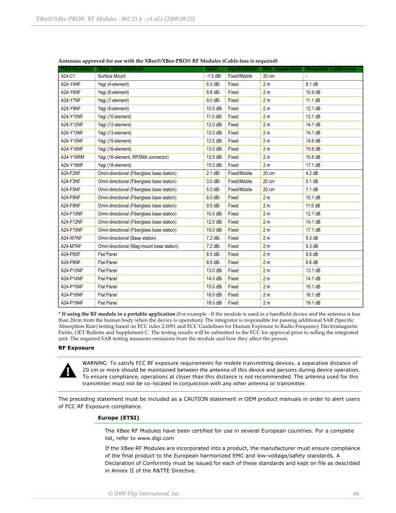
XBee®/XBee‐PRO® RF Modules ‐ 802.15.4 ‐ v1.xEx [2009.09.23]
© 2009 Digi Internatonal, Inc. 66
Antennas approved for use with the XBee®/XBee‐PRO® RF Modules (Cable‐loss is required)
* If using the RF module in a portable application (For example ‐ If the module is used in a handheld device and the antenna is less than 20cm from the human body when the device is operation): The integrator is responsible for passing additional SAR (Specific Absorption Rate) testing based on FCC rules 2.1091 and FCC Guidelines for Human Exposure to Radio Frequency Electromagnetic Fields, OET Bulletin and Supplement C. The testing results will be submitted to the FCC for approval prior to selling the integrated unit. The required SAR testing measures emissions from the module and how they affect the person.
RF Exposure
WARNING: To satisfy FCC RF exposure requirements for mobile transmitting devices, a separation distance of 20 cm or more should be maintained between the antenna of this device and persons during device operation. To ensure compliance, operations at closer than this distance is not recommended. The antenna used for this transmitter must not be co-located in conjunction with any other antenna or transmitter.
The preceding statement must be included as a CAUTION statement in OEM product manuals in order to alert users of FCC RF Exposure compliance.
Europe (ETSI)
The XBee RF Modules have been certified for use in several European countries. For a complete list, refer to www.digi.com
If the XBee RF Modules are incorporated into a product, the manufacturer must ensure compliance of the final product to the European harmonized EMC and low-voltage/safety standards. A Declaration of Conformity must be issued for each of these standards and kept on file as described in Annex II of the R&TTE Directive.
Part Number Type (Description) Gain Application* Min. Separation Required Cable-lossA24-C1 Surface Mount -1.5 dBi Fixed/Mobile 20 cm -A24-Y4NF Yagi (4-element) 6.0 dBi Fixed 2 m 8.1 dBA24-Y6NF Yagi (6-element) 8.8 dBi Fixed 2 m 10.9 dBA24-Y7NF Yagi (7-element) 9.0 dBi Fixed 2 m 11.1 dBA24-Y9NF Yagi (9-element) 10.0 dBi Fixed 2 m 12.1 dBA24-Y10NF Yagi (10-element) 11.0 dBi Fixed 2 m 13.1 dBA24-Y12NF Yagi (12-element) 12.0 dBi Fixed 2 m 14.1 dBA24-Y13NF Yagi (13-element) 12.0 dBi Fixed 2 m 14.1 dBA24-Y15NF Yagi (15-element) 12.5 dBi Fixed 2 m 14.6 dBA24-Y16NF Yagi (16-element) 13.5 dBi Fixed 2 m 15.6 dBA24-Y16RM Yagi (16-element, RPSMA connector) 13.5 dBi Fixed 2 m 15.6 dBA24-Y18NF Yagi (18-element) 15.0 dBi Fixed 2 m 17.1 dBA24-F2NF Omni-directional (Fiberglass base station) 2.1 dBi Fixed/Mobile 20 cm 4.2 dBA24-F3NF Omni-directional (Fiberglass base station) 3.0 dBi Fixed/Mobile 20 cm 5.1 dBA24-F5NF Omni-directional (Fiberglass base station) 5.0 dBi Fixed/Mobile 20 cm 7.1 dBA24-F8NF Omni-directional (Fiberglass base station) 8.0 dBi Fixed 2 m 10.1 dBA24-F9NF Omni-directional (Fiberglass base station) 9.5 dBi Fixed 2 m 11.6 dBA24-F10NF Omni-directional (Fiberglass base station) 10.0 dBi Fixed 2 m 12.1 dBA24-F12NF Omni-directional (Fiberglass base station) 12.0 dBi Fixed 2 m 14.1 dBA24-F15NF Omni-directional (Fiberglass base station) 15.0 dBi Fixed 2 m 17.1 dBA24-W7NF Omni-directional (Base station) 7.2 dBi Fixed 2 m 9.3 dBA24-M7NF Omni-directional (Mag-mount base station) 7.2 dBi Fixed 2 m 9.3 dBA24-P8SF Flat Panel 8.5 dBi Fixed 2 m 8.6 dBA24-P8NF Flat Panel 8.5 dBi Fixed 2 m 8.6 dBA24-P13NF Flat Panel 13.0 dBi Fixed 2 m 13.1 dBA24-P14NF Flat Panel 14.0 dBi Fixed 2 m 14.1 dBA24-P15NF Flat Panel 15.0 dBi Fixed 2 m 15.1 dBA24-P16NF Flat Panel 16.0 dBi Fixed 2 m 16.1 dBA24-P19NF Flat Panel 19.0 dBi Fixed 2 m 19.1 dB
XBee®/XBee‐PRO® RF Modules ‐ 802.15.4 ‐ v1.xEx [2009.09.23]
© 2009 Digi Internatonal, Inc. 67
Furthermore, the manufacturer must maintain a copy of the XBee user manual documentation and ensure the final product does not exceed the specified power ratings, antenna specifications, and/or installation requirements as specified in the user manual. If any of these specifications are exceeded in the final product, a submission must be made to a notified body for compliance testing to all required standards.
OEM Labeling Requirements
The 'CE' marking must be affixed to a visible location on the OEM product.
CE Labeling RequirementsThe CE mark shall consist of the initials "CE" taking the following form:
• If the CE marking is reduced or enlarged, the proportions given in the above graduated draw-ing must be respected.
• The CE marking must have a height of at least 5mm except where this is not possible on account of the nature of the apparatus.
• The CE marking must be affixed visibly, legibly, and indelibly.
Restrictions
Power Output: When operating in Europe, XBee-PRO 802.15.4 modules must operate at or below a transmit power output level of 10dBm. Customers have two choices for transmitting at or below 10dBm:
a. Order the standard XBee-PRO module and change the PL command to 0 (10dBm)
b. Order the International variant of the XBee-PRO module, which has a maximum transmit output power of 10dBm (@ PL=4).
Additionally, European regulations stipulate an EIRP power maximum of 12.86 dBm (19 mW) for the XBee-PRO and 12.11 dBm for the XBee when integrating antennas.
France: Outdoor use limited to 10 mW EIRP within the band 2454-2483.5 MHz.
Norway: Norway prohibits operation near Ny-Alesund in Svalbard. More information can be found at the Norway Posts and Telecommunications site (www.npt.no).
Declarations of Conformity
Digi has issued Declarations of Conformity for the XBee RF Modules concerning emissions, EMC and safety. Files can be obtained by contacting Digi Support.
Important Note:
Digi does not list the entire set of standards that must be met for each country. Digi customers assume full responsibility for learning and meeting the required guidelines for each country in their distribution market. For more information relating to European compliance of an OEM product incorporating the XBee RF Module, contact Digi, or refer to the following web sites:
CEPT ERC 70-03E - Technical Requirements, European restrictions and general requirements: Available at www.ero.dk/.
R&TTE Directive - Equipment requirements, placement on market: Available at www.ero.dk/.
Approved Antennas
When integrating high-gain antennas, European regulations stipulate EIRP power maximums. Use the following guidelines to determine which antennas to design into an application.
XBee-PRO RF Module
The following antenna types have been tested and approved for use with the XBee Module:
Antenna Type: Yagi RF module was tested and approved with 15 dBi antenna gain with 1 dB cable-loss (EIRP Maxi-mum of 14 dBm). Any Yagi type antenna with 14 dBi gain or less can be used with no cable-loss.
Antenna Type: Omni-directional RF module was tested and approved with 15 dBi antenna gain with 1 dB cable-loss (EIRP Maxi-
XBee®/XBee‐PRO® RF Modules ‐ 802.15.4 ‐ v1.xEx [2009.09.23]
© 2009 Digi Internatonal, Inc. 68
mum of 14 dBm). Any Omni-directional type antenna with 14 dBi gain or less can be used with no cable-loss.
Antenna Type: Flat Panel RF module was tested and approved with 19 dBi antenna gain with 4.8 dB cable-loss (EIRP Maxi-mum of 14.2 dBm). Any Flat Panel type antenna with 14.2 dBi gain or less can be used with no cable-loss.
XBee-PRO RF Module (@ 10 dBm Transmit Power, PL parameter value must equal 0, or use Inter-national variant)
The following antennas have been tested and approved for use with the embedded XBee-PRO RF Module:
• Dipole (2.1 dBi, Omni-directional, Articulated RPSMA, Digi part number A24-HABSM)
• Chip Antenna (-1.5 dBi)
• Attached Monopole Whip (1.5 dBi)
The RF modem encasement was designed to accommodate the RPSMA antenna option.
Canada (IC)
Labeling Requirements
Labeling requirements for Industry Canada are similar to those of the FCC. A clearly visible label on the outside of the final product enclosure must display the following text:
Contains Model XBee Radio, IC: 4214A-XBEE Contains Model XBee-PRO Radio, IC: 4214A-XBEEPRO
The integrator is responsible for its product to comply with IC ICES-003 & FCC Part 15, Sub. B - Unintentional Radiators. ICES-003 is the same as FCC Part 15 Sub. B and Industry Canada accepts FCC test report or CISPR 22 test report for compliance with ICES-003.
Japan
In order to gain approval for use in Japan, the XBee RF module or the International variant of the XBee-PRO RF module (which has 10 dBm transmit output power) must be used.
Labeling Requirements
A clearly visible label on the outside of the final product enclosure must display the following text:
ID: 005NYCA0378
© 2009 Digi International Inc. 69
Appendix B. Additional Information
1-Year Warranty
XBee®/XBee-PRO® RF Modules from Digi Intenational, Inc. (the "Product") are warranted against defects in materials and workmanship under normal use, for a period of 1-year from the date of purchase. In the event of a product failure due to materials or workmanship, Digi will repair or replace the defective product. For warranty service, return the defective product to Digi, shipping prepaid, for prompt repair or replacement.
The foregoing sets forth the full extent of Digi's warranties regarding the Product. Repair or replacement at Digi's option is the exclusive remedy. THIS WARRANTY IS GIVEN IN LIEU OF ALL OTHER WARRANTIES, EXPRESS OR IMPLIED, AND DIGI SPECIFICALLY DISCLAIMS ALL WARRAN-TIES OF MERCHANTABILITY OR FITNESS FOR A PARTICULAR PURPOSE. IN NO EVENT SHALL DIGI, ITS SUPPLIERS OR LICENSORS BE LIABLE FOR DAMAGES IN EXCESS OF THE PURCHASE PRICE OF THE PRODUCT, FOR ANY LOSS OF USE, LOSS OF TIME, INCONVENIENCE, COMMERCIAL LOSS, LOST PROFITS OR SAVINGS, OR OTHER INCIDENTAL, SPECIAL OR CONSEQUENTIAL DAMAGES ARISING OUT OF THE USE OR INABILITY TO USE THE PRODUCT, TO THE FULL EXTENT SUCH MAY BE DISCLAIMED BY LAW. SOME STATES DO NOT ALLOW THE EXCLUSION OR LIMITATION OF INCI-DENTAL OR CONSEQUENTIAL DAMAGES. THEREFORE, THE FOREGOING EXCLUSIONS MAY NOT APPLY IN ALL CASES. This warranty provides specific legal rights. Other rights which vary from state to state may also apply.
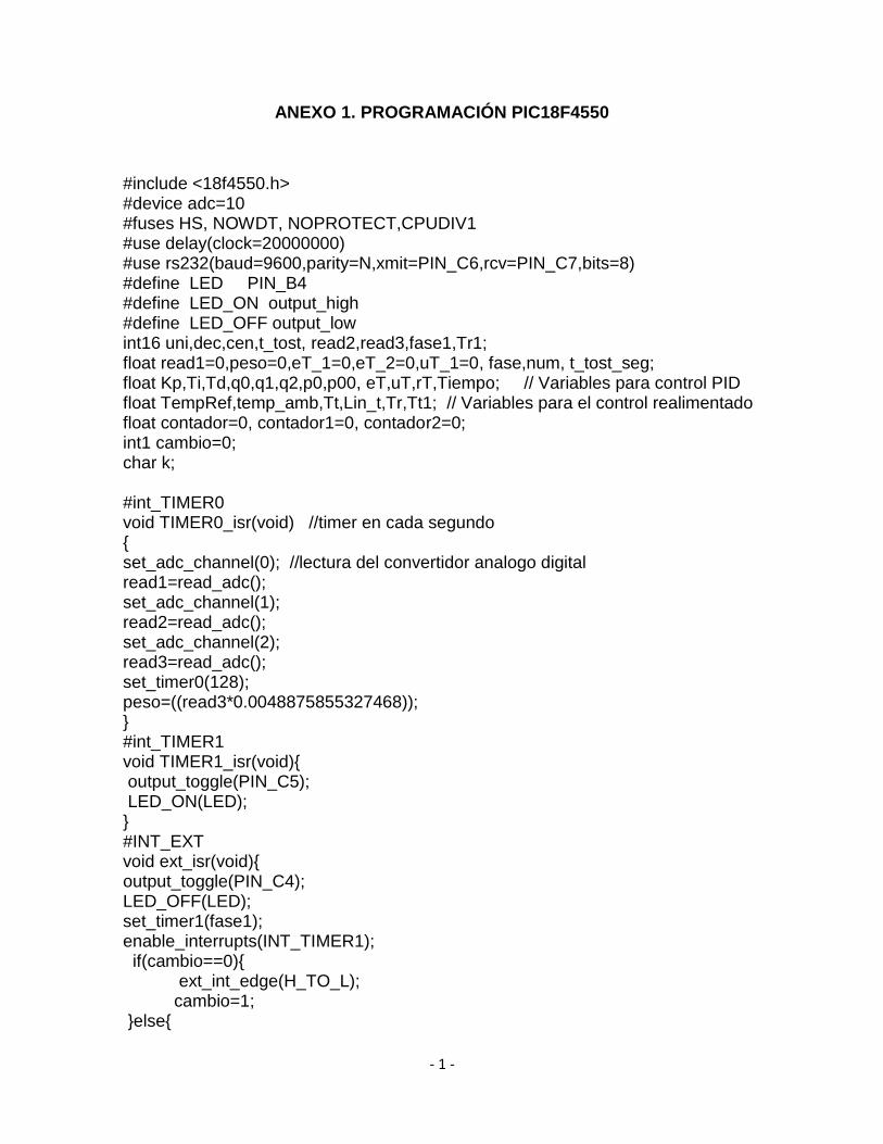
- 1 -
ANEXO 1. PROGRAMACIÓN PIC18F4550
#include <18f4550.h> #device adc=10 #fuses HS, NOWDT, NOPROTECT,CPUDIV1 #use delay(clock=20000000) #use rs232(baud=9600,parity=N,xmit=PIN_C6,rcv=PIN_C7,bits=8) #define LED PIN_B4 #define LED_ON output_high #define LED_OFF output_low int16 uni,dec,cen,t_tost, read2,read3,fase1,Tr1; float read1=0,peso=0,eT_1=0,eT_2=0,uT_1=0, fase,num, t_tost_seg; float Kp,Ti,Td,q0,q1,q2,p0,p00, eT,uT,rT,Tiempo; // Variables para control PID float TempRef,temp_amb,Tt,Lin_t,Tr,Tt1; // Variables para el control realimentado float contador=0, contador1=0, contador2=0; int1 cambio=0; char k; #int_TIMER0 void TIMER0_isr(void) //timer en cada segundo set_adc_channel(0); //lectura del convertidor analogo digital read1=read_adc(); set_adc_channel(1); read2=read_adc(); set_adc_channel(2); read3=read_adc(); set_timer0(128); peso=((read3*0.0048875855327468)); #int_TIMER1 void TIMER1_isr(void) output_toggle(PIN_C5); LED_ON(LED); #INT_EXT void ext_isr(void) output_toggle(PIN_C4); LED_OFF(LED); set_timer1(fase1); enable_interrupts(INT_TIMER1); if(cambio==0)
ext_int_edge(H_TO_L); cambio=1; else
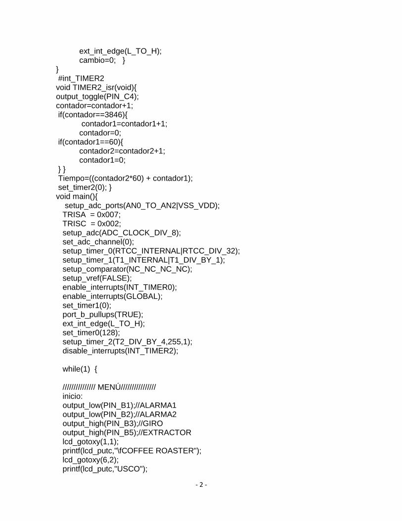
- 2 -
ext_int_edge(L_TO_H); cambio=0; #int_TIMER2 void TIMER2_isr(void) output_toggle(PIN_C4); contador=contador+1; if(contador==3846)
contador1=contador1+1; contador=0; if(contador1==60) contador2=contador2+1; contador1=0; Tiempo=((contador2*60) + contador1); set_timer2(0); void main() setup_adc_ports(AN0_TO_AN2|VSS_VDD); TRISA = 0x007; TRISC = 0x002; setup_adc(ADC_CLOCK_DIV_8); set_adc_channel(0); setup_timer_0(RTCC_INTERNAL|RTCC_DIV_32); setup_timer_1(T1_INTERNAL|T1_DIV_BY_1); setup_comparator(NC_NC_NC_NC); setup_vref(FALSE); enable_interrupts(INT_TIMER0); enable_interrupts(GLOBAL); set_timer1(0); port_b_pullups(TRUE); ext_int_edge(L_TO_H); set_timer0(128); setup_timer_2(T2_DIV_BY_4,255,1); disable_interrupts(INT_TIMER2); while(1) /////////////// MENÚ//////////////// inicio: output_low(PIN_B1);//ALARMA1 output_low(PIN_B2);//ALARMA2 output_high(PIN_B3);//GIRO output_high(PIN_B5);//EXTRACTOR lcd_gotoxy(1,1); printf(lcd_putc,"\fCOFFEE ROASTER"); lcd_gotoxy(6,2); printf(lcd_putc,"USCO");
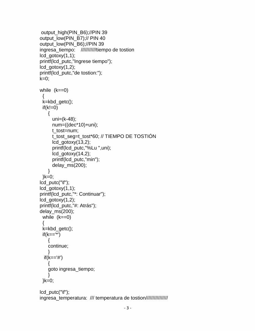
- 3 -
output_high(PIN_B6);//PIN 39 output_low(PIN_B7);// PIN 40 output_low(PIN_B6);//PIN 39 ingresa_tiempo: ///////////tiempo de tostion lcd_gotoxy(1,1); printf(lcd_putc,"Ingrese tiempo"); lcd_gotoxy(1,2); printf(lcd_putc,"de tostion:"); k=0; while (k==0) k=kbd_getc(); if(k!=0) uni=(k-48); num=((dec*10)+uni); t_tost=num; t_tost_seg=t_tost*60; // TIEMPO DE TOSTIÓN lcd_gotoxy(13,2); printf(lcd_putc,"%Lu ",uni); lcd_gotoxy(14,2); printf(lcd_putc,"min"); delay_ms(200); k=0; lcd_putc("\f"); lcd_gotoxy(1,1); printf(lcd_putc,"*: Continuar"); lcd_gotoxy(1,2); printf(lcd_putc,"#: Atrás"); delay_ms(200); while (k==0) k=kbd_getc(); if(k=='*') continue; if(k=='#') goto ingresa_tiempo; k=0; lcd_putc("\f"); ingresa_temperatura: /// temperatura de tostion////////////////
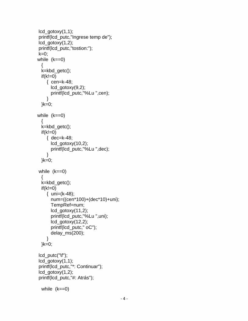
- 4 -
lcd_gotoxy(1,1); printf(lcd_putc,"Ingrese temp de"); lcd_gotoxy(1,2); printf(lcd_putc,"tostion:"); k=0; while (k==0) k=kbd_getc(); if(k!=0) cen=k-48; lcd_gotoxy(9,2); printf(lcd_putc,"%Lu ",cen); k=0; while (k==0) k=kbd_getc(); if(k!=0) dec=k-48; lcd_gotoxy(10,2); printf(lcd_putc,"%Lu ",dec); k=0; while (k==0) k=kbd_getc(); if(k!=0) uni=(k-48); num=((cen*100)+(dec*10)+uni); TempRef=num; lcd_gotoxy(11,2); printf(lcd_putc,"%Lu ",uni); lcd_gotoxy(12,2); printf(lcd_putc," oC"); delay_ms(200); k=0; lcd_putc("\f"); lcd_gotoxy(1,1); printf(lcd_putc,"*: Continuar"); lcd_gotoxy(1,2); printf(lcd_putc,"#: Atrás"); while (k==0)
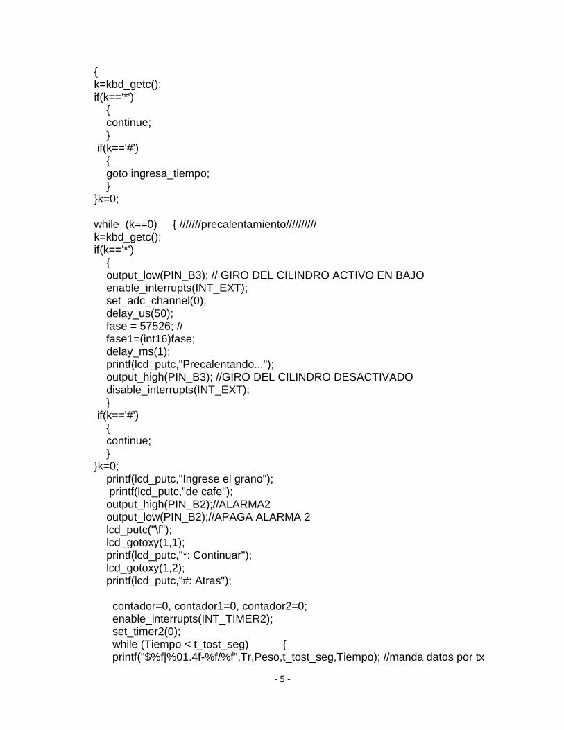
- 5 -
k=kbd_getc(); if(k=='*') continue; if(k=='#') goto ingresa_tiempo; k=0; while (k==0) ///////precalentamiento////////// k=kbd_getc(); if(k=='*') output_low(PIN_B3); // GIRO DEL CILINDRO ACTIVO EN BAJO enable_interrupts(INT_EXT); set_adc_channel(0); delay_us(50); fase = 57526; // fase1=(int16)fase; delay_ms(1); printf(lcd_putc,"Precalentando..."); output_high(PIN_B3); //GIRO DEL CILINDRO DESACTIVADO disable_interrupts(INT_EXT); if(k=='#') continue; k=0; printf(lcd_putc,"Ingrese el grano"); printf(lcd_putc,"de cafe"); output_high(PIN_B2);//ALARMA2 output_low(PIN_B2);//APAGA ALARMA 2 lcd_putc("\f"); lcd_gotoxy(1,1); printf(lcd_putc,"*: Continuar"); lcd_gotoxy(1,2); printf(lcd_putc,"#: Atras"); contador=0, contador1=0, contador2=0; enable_interrupts(INT_TIMER2); set_timer2(0); while (Tiempo < t_tost_seg) printf("$%f|%01.4f-%f/%f",Tr,Peso,t_tost_seg,Tiempo); //manda datos por tx
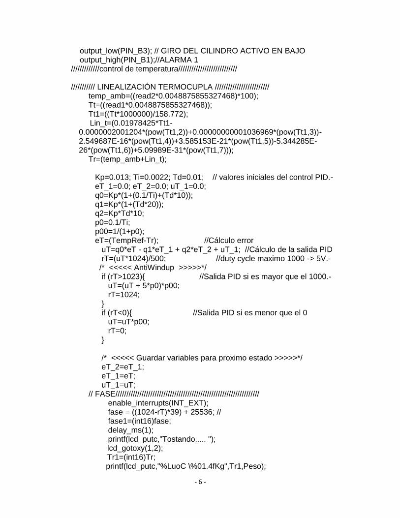
- 6 -
output_low(PIN_B3); // GIRO DEL CILINDRO ACTIVO EN BAJO output_high(PIN_B1);//ALARMA 1 /////////////control de temperatura/////////////////////////// /////////// LINEALIZACIÓN TERMOCUPLA ///////////////////////// temp_amb=((read2*0.0048875855327468)*100); Tt=((read1*0.0048875855327468)); Tt1=((Tt*1000000)/158.772);
Lin_t=(0.01978425*Tt1-0.0000002001204*(pow(Tt1,2))+0.00000000001036969*(pow(Tt1,3))-2.549687E-16*(pow(Tt1,4))+3.585153E-21*(pow(Tt1,5))-5.344285E-26*(pow(Tt1,6))+5.09989E-31*(pow(Tt1,7)));
Tr=(temp_amb+Lin_t); Kp=0.013; Ti=0.0022; Td=0.01; // valores iniciales del control PID.- eT_1=0.0; eT_2=0.0; uT_1=0.0; q0=Kp*(1+(0.1/Ti)+(Td*10)); q1=Kp*(1+(Td*20)); q2=Kp*Td*10; p0=0.1/Ti; p00=1/(1+p0); eT=(TempRef-Tr); //Cálculo error uT=q0*eT - q1*eT_1 + q2*eT_2 + uT_1; //Cálculo de la salida PID rT=(uT*1024)/500; //duty cycle maximo 1000 -> 5V.- /* <<<<< AntiWindup >>>>>*/ if (rT>1023) //Salida PID si es mayor que el 1000.- uT=(uT + 5*p0)*p00; rT=1024; if (rT<0) //Salida PID si es menor que el 0 uT=uT*p00; rT=0; /* <<<<< Guardar variables para proximo estado >>>>>*/ eT_2=eT_1; eT_1=eT; uT_1=uT; // FASE////////////////////////////////////////////////////////////////// enable_interrupts(INT_EXT); fase = ((1024-rT)*39) + 25536; // fase1=(int16)fase; delay_ms(1); printf(lcd_putc,"Tostando..... ");
lcd_gotoxy(1,2); Tr1=(int16)Tr;
printf(lcd_putc,"%LuoC \%01.4fKg",Tr1,Peso);
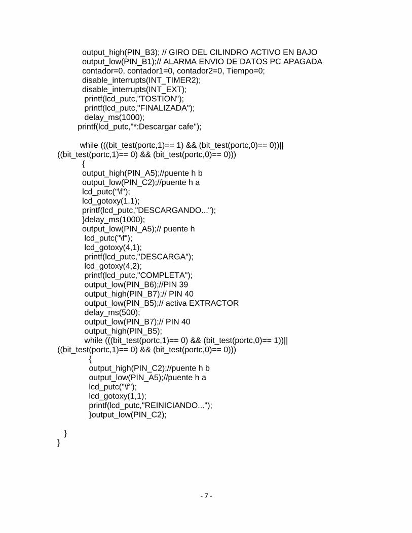
- 7 -
output_high(PIN_B3); // GIRO DEL CILINDRO ACTIVO EN BAJO output_low(PIN_B1);// ALARMA ENVIO DE DATOS PC APAGADA contador=0, contador1=0, contador2=0, Tiempo=0; disable_interrupts(INT_TIMER2); disable_interrupts(INT_EXT); printf(lcd_putc,"TOSTION"); printf(lcd_putc,"FINALIZADA"); delay_ms(1000); printf(lcd_putc,"*:Descargar cafe"); while (((bit_test(portc,1)== 1) && (bit_test(portc,0)== 0))|| ((bit_test(portc,1)== 0) && (bit_test(portc,0)== 0))) output_high(PIN_A5);//puente h b output_low(PIN_C2);//puente h a lcd_putc("\f"); lcd_gotoxy(1,1); printf(lcd_putc,"DESCARGANDO..."); delay_ms(1000); output_low(PIN_A5);// puente h lcd_putc("\f"); lcd_gotoxy(4,1); printf(lcd_putc,"DESCARGA"); lcd_gotoxy(4,2); printf(lcd_putc,"COMPLETA"); output_low(PIN_B6);//PIN 39 output_high(PIN_B7);// PIN 40 output_low(PIN_B5);// activa EXTRACTOR delay_ms(500); output_low(PIN_B7);// PIN 40 output_high(PIN_B5); while (((bit_test(portc,1)== 0) && (bit_test(portc,0)== 1))|| ((bit_test(portc,1)== 0) && (bit_test(portc,0)== 0))) output_high(PIN_C2);//puente h b output_low(PIN_A5);//puente h a lcd_putc("\f"); lcd_gotoxy(1,1); printf(lcd_putc,"REINICIANDO..."); output_low(PIN_C2);
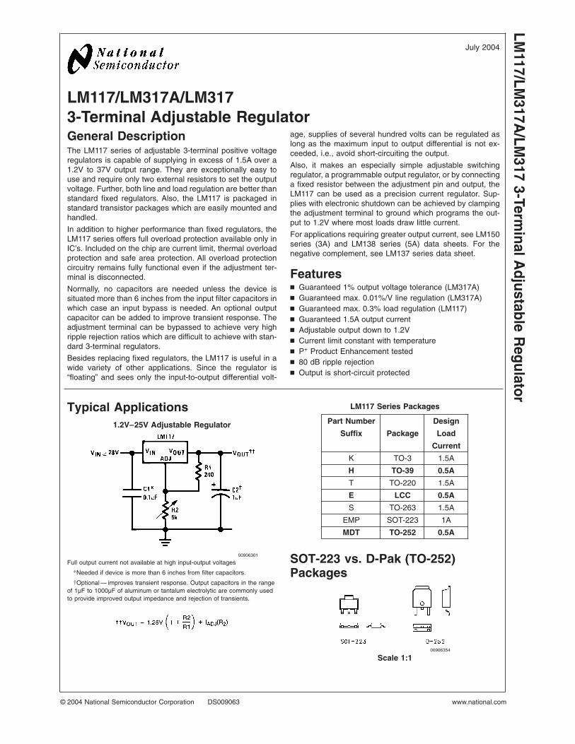
LM117/LM317A/LM3173-Terminal Adjustable RegulatorGeneral DescriptionThe LM117 series of adjustable 3-terminal positive voltageregulators is capable of supplying in excess of 1.5A over a1.2V to 37V output range. They are exceptionally easy touse and require only two external resistors to set the outputvoltage. Further, both line and load regulation are better thanstandard fixed regulators. Also, the LM117 is packaged instandard transistor packages which are easily mounted andhandled.
In addition to higher performance than fixed regulators, theLM117 series offers full overload protection available only inIC’s. Included on the chip are current limit, thermal overloadprotection and safe area protection. All overload protectioncircuitry remains fully functional even if the adjustment ter-minal is disconnected.
Normally, no capacitors are needed unless the device issituated more than 6 inches from the input filter capacitors inwhich case an input bypass is needed. An optional outputcapacitor can be added to improve transient response. Theadjustment terminal can be bypassed to achieve very highripple rejection ratios which are difficult to achieve with stan-dard 3-terminal regulators.
Besides replacing fixed regulators, the LM117 is useful in awide variety of other applications. Since the regulator is“floating” and sees only the input-to-output differential volt-
age, supplies of several hundred volts can be regulated aslong as the maximum input to output differential is not ex-ceeded, i.e., avoid short-circuiting the output.
Also, it makes an especially simple adjustable switchingregulator, a programmable output regulator, or by connectinga fixed resistor between the adjustment pin and output, theLM117 can be used as a precision current regulator. Sup-plies with electronic shutdown can be achieved by clampingthe adjustment terminal to ground which programs the out-put to 1.2V where most loads draw little current.
For applications requiring greater output current, see LM150series (3A) and LM138 series (5A) data sheets. For thenegative complement, see LM137 series data sheet.
Featuresn Guaranteed 1% output voltage tolerance (LM317A)n Guaranteed max. 0.01%/V line regulation (LM317A)n Guaranteed max. 0.3% load regulation (LM117)n Guaranteed 1.5A output currentn Adjustable output down to 1.2Vn Current limit constant with temperaturen P+ Product Enhancement testedn 80 dB ripple rejectionn Output is short-circuit protected
Typical Applications1.2V–25V Adjustable Regulator
00906301
Full output current not available at high input-output voltages
*Needed if device is more than 6 inches from filter capacitors.
†Optional — improves transient response. Output capacitors in the rangeof 1µF to 1000µF of aluminum or tantalum electrolytic are commonly usedto provide improved output impedance and rejection of transients.
LM117 Series Packages
Part Number Design
Suffix Package Load
Current
K TO-3 1.5A
H TO-39 0.5A
T TO-220 1.5A
E LCC 0.5A
S TO-263 1.5A
EMP SOT-223 1A
MDT TO-252 0.5A
SOT-223 vs. D-Pak (TO-252)Packages
00906354
Scale 1:1
July 2004LM
117/LM317A
/LM317
3-TerminalA
djustableR
egulator
© 2004 National Semiconductor Corporation DS009063 www.national.com
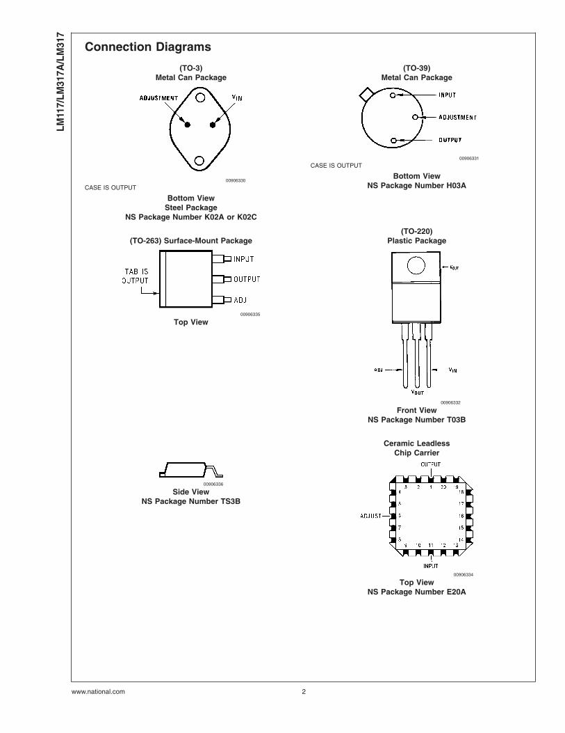
Connection Diagrams
(TO-3)Metal Can Package
(TO-39)Metal Can Package
00906330
CASE IS OUTPUT
Bottom ViewSteel Package
NS Package Number K02A or K02C
00906331
CASE IS OUTPUT
Bottom ViewNS Package Number H03A
(TO-263) Surface-Mount Package(TO-220)
Plastic Package
00906335
Top View
00906332
Front ViewNS Package Number T03B
Ceramic LeadlessChip Carrier
00906336
Side ViewNS Package Number TS3B
00906334
Top ViewNS Package Number E20A
LM11
7/LM
317A
/LM
317
www.national.com 2
Connection Diagrams (Continued)
4-Lead SOT-223 TO-252 (D-Pak)
00906359
Front ViewNS Package Number MP04A
00906366
Front ViewNS Package Number TD03B
Ordering Information
Package Temperature Range Part Number Package Marking Transport Media NSCDrawing
Metal Can(TO-3)
−55˚C ≤ TJ ≤ +150˚C LM117K STEEL LM117K STEEL P+ 50 Per Bag K02A
0˚C ≤ TJ ≤ +125˚C LM317K STEEL LM317K STEEL P+ 50 Per Bag
−55˚C ≤ TJ ≤ +150˚C LM117K/883 LM117K/883 50 Per Bag K02C
Metal Can(TO-39)
−55˚C ≤ TJ ≤ +150˚C LM117H LM117H P+ 500 Per Box H03A
−55˚C ≤ TJ ≤ +150˚C LM117H/883 LM117H/883 20 Per Tray
−40˚C ≤ TJ ≤ +125˚C LM317AH LM317AH P+ 500 Per Box
0˚C ≤ TJ ≤ +125˚C LM317H LM317H P+ 500 Per Box
TO-2203- Lead
−40˚C ≤ TJ ≤ +125˚C LM317AT LM317AT P+ 45 Units/Rail T03B
0˚C ≤ TJ ≤ +125˚C LM317T LM317T P+ 45 Units/Rail
TO-2633- Lead
0˚C ≤ TJ ≤ +125˚C LM317S LM317S P+ 45 Units/Rail TS3B
LM317SX 500 Units Tape and Reel
LCC −55˚C ≤ TJ ≤ +150˚C LM117E/883 LM117E/883 50 Units/Rail E20A
SOT-2234- Lead
0˚C ≤ TJ ≤ +125˚C LM317EMP N01A 1k Units Tape and Reel MP04A
LM317EMPX 2k Units Tape and Reel
−40˚C ≤ TJ ≤ +125˚C LM317AEMP N07A 1k Units Tape and Reel
LM317AEMPX 2k Units Tape and Reel
D- Pack3- Lead
0˚C ≤ TJ ≤ +125˚C LM317MDT LM317MDT 75 Units/Rail TD03B
LM317MDTX 2.5k Units Tape and Reel
−40˚C ≤ TJ ≤ +125˚C LM317AMDT LM317AMDT 75 Units/Rail
LM317AMDTX 2.5k Units Tape and Reel
LM117/LM
317A/LM
317
www.national.com3
Absolute Maximum Ratings (Note 1)
If Military/Aerospace specified devices are required,please contact the National Semiconductor Sales Office/Distributors for availability and specifications.
Power Dissipation Internally Limited
Input-Output Voltage Differential +40V, −0.3V
Storage Temperature −65˚C to +150˚C
Lead Temperature
Metal Package (Soldering, 10 seconds) 300˚C
Plastic Package (Soldering, 4 seconds) 260˚C
ESD Tolerance (Note 5) 3 kV
Operating Temperature RangeLM117 −55˚C ≤ TJ ≤ +150˚C
LM317A −40˚C ≤ TJ ≤ +125˚C
LM317 0˚C ≤ TJ ≤ +125˚C
Preconditioning
Thermal Limit Burn-In All Devices 100%
Electrical Characteristics (Note 3)
Specifications with standard type face are for TJ = 25˚C, and those with boldface type apply over full Operating Tempera-ture Range. Unless otherwise specified, VIN − VOUT = 5V, and IOUT = 10 mA.
Parameter Conditions LM117 (Note 2) Units
Min Typ Max
Reference Voltage V
3V ≤ (VIN − VOUT) ≤ 40V, 1.20 1.25 1.30 V
10 mA ≤ IOUT ≤ IMAX, P ≤ PMAX
Line Regulation 3V ≤ (VIN − VOUT) ≤ 40V (Note 4) 0.01 0.02 %/V
0.02 0.05 %/V
Load Regulation 10 mA ≤ IOUT ≤ IMAX (Note 4) 0.1 0.3 %
0.3 1 %
Thermal Regulation 20 ms Pulse 0.03 0.07 %/W
Adjustment Pin Current 50 100 µA
Adjustment Pin Current Change 10 mA ≤ IOUT ≤ IMAX 0.2 5 µA
3V ≤ (VIN − VOUT) ≤ 40V
Temperature Stability TMIN ≤ TJ ≤ TMAX 1 %
Minimum Load Current (VIN − VOUT) = 40V 3.5 5 mA
Current Limit (VIN − VOUT) ≤ 15V
K Package 1.5 2.2 3.4 A
H Package 0.5 0.8 1.8 A
(VIN − VOUT) = 40V
K Package 0.3 0.4 A
H Package 0.15 0.2 A
RMS Output Noise, % of VOUT 10 Hz ≤ f ≤ 10 kHz 0.003 %
Ripple Rejection Ratio VOUT = 10V, f = 120 Hz, 65 dB
CADJ = 0 µF
VOUT = 10V, f = 120 Hz, 66 80 dB
CADJ = 10 µF
Long-Term Stability TJ = 125˚C, 1000 hrs 0.3 1 %
Thermal Resistance, K Package 2.3 3 ˚C/W
Junction-to-Case H Package 12 15 ˚C/W
E Package ˚C/W
Thermal Resistance, Junction- K Package 35 ˚C/W
to-Ambient (No Heat Sink) H Package 140 ˚C/W
E Package ˚C/W
LM11
7/LM
317A
/LM
317
www.national.com 4
Electrical Characteristics (Note 3)
Specifications with standard type face are for TJ = 25˚C, and those with boldface type apply over full Operating Tempera-ture Range. Unless otherwise specified, VIN − VOUT = 5V, and IOUT = 10 mA.
Parameter Conditions LM317A LM317 Units
Min Typ Max Min Typ Max
Reference Voltage 1.238 1.250 1.262 V
3V ≤ (VIN − VOUT) ≤ 40V, 1.225 1.250 1.270 1.20 1.25 1.30 V
10 mA ≤ IOUT ≤ IMAX, P ≤ PMAX
Line Regulation 3V ≤ (VIN − VOUT) ≤ 40V (Note 4) 0.005 0.01 0.01 0.04 %/V
0.01 0.02 0.02 0.07 %/V
Load Regulation 10 mA ≤ IOUT ≤ IMAX (Note 4) 0.1 0.5 0.1 0.5 %
0.3 1 0.3 1.5 %
Thermal Regulation 20 ms Pulse 0.04 0.07 0.04 0.07 %/W
Adjustment Pin Current 50 100 50 100 µA
Adjustment Pin CurrentChange
10 mA ≤ IOUT ≤ IMAX 0.2 5 0.2 5 µA
3V ≤ (VIN − VOUT) ≤ 40V
Temperature Stability TMIN ≤ TJ ≤ TMAX 1 1 %
Minimum Load Current (VIN − VOUT) = 40V 3.5 10 3.5 10 mA
Current Limit (VIN − VOUT) ≤ 15V
K, T, S Packages 1.5 2.2 3.4 1.5 2.2 3.4 A
H PackageMP Package
0.51.5
0.82.2
1.83.4
0.51.5
0.82.2
1.83.4
AA
(VIN − VOUT) = 40V
K, T, S Packages 0.15 0.4 0.15 0.4 A
H PackageMP Package
0.0750.15
0.20.4
0.0750.15
0.20.4
AA
RMS Output Noise, % of VOUT 10 Hz ≤ f ≤ 10 kHz 0.003 0.003 %
Ripple Rejection Ratio VOUT = 10V, f = 120 Hz, 65 65 dB
CADJ = 0 µF
VOUT = 10V, f = 120 Hz, 66 80 66 80 dB
CADJ = 10 µF
Long-Term Stability TJ = 125˚C, 1000 hrs 0.3 1 0.3 1 %
Thermal Resistance,Junction-to-Case
K PackageMDT Package
2.35
3 ˚C/W˚C/W
H Package 12 15 12 15 ˚C/W
T PackageMP Package
423.5
5 423.5
˚C/W˚C/W
Thermal Resistance,Junction-to-Ambient (No HeatSink)
K PackageMDT Package(Note 6)
35 3592
˚C/W˚C/W
H Package 140 140 ˚C/W
T Package 50 50 ˚C/W
S Package (Note 6) 50 50 ˚C/W
Note 1: Absolute Maximum Ratings indicate limits beyond which damage to the device may occur. Operating Ratings indicate conditions for which the device isintended to be functional, but do not guarantee specific performance limits. For guaranteed specifications and test conditions, see the Electrical Characteristics. Theguaranteed specifications apply only for the test conditions listed.
Note 2: Refer to RETS117H drawing for the LM117H, or the RETS117K for the LM117K military specifications.
Note 3: Although power dissipation is internally limited, these specifications are applicable for maximum power dissipations of 2W for the TO-39 and SOT-223 and20W for the TO-3, TO-220, and TO-263. IMAX is 1.5A for the TO-3, TO-220, and TO-263 packages, 0.5A for the TO-39 package and 1A for the SOT-223 Package.All limits (i.e., the numbers in the Min. and Max. columns) are guaranteed to National’s AOQL (Average Outgoing Quality Level).
Note 4: Regulation is measured at a constant junction temperature, using pulse testing with a low duty cycle. Changes in output voltage due to heating effects arecovered under the specifications for thermal regulation.
Note 5: Human body model, 100 pF discharged through a 1.5 kΩ resistor.
Note 6: If the TO-263 or TO-252 packages are used, the thermal resistance can be reduced by increasing the PC board copper area thermally connected to thepackage. Using 0.5 square inches of copper area. θJA is 50˚C/W; with 1 square inch of copper area, θJA is 37˚C/W; and with 1.6 or more square inches of copperarea, θJA is 32˚C/W. If the SOT-223 package is used, the thermal resistance can be reduced by increasing the PC board copper area (see applications hints forheatsinking).
LM117/LM
317A/LM
317
www.national.com5
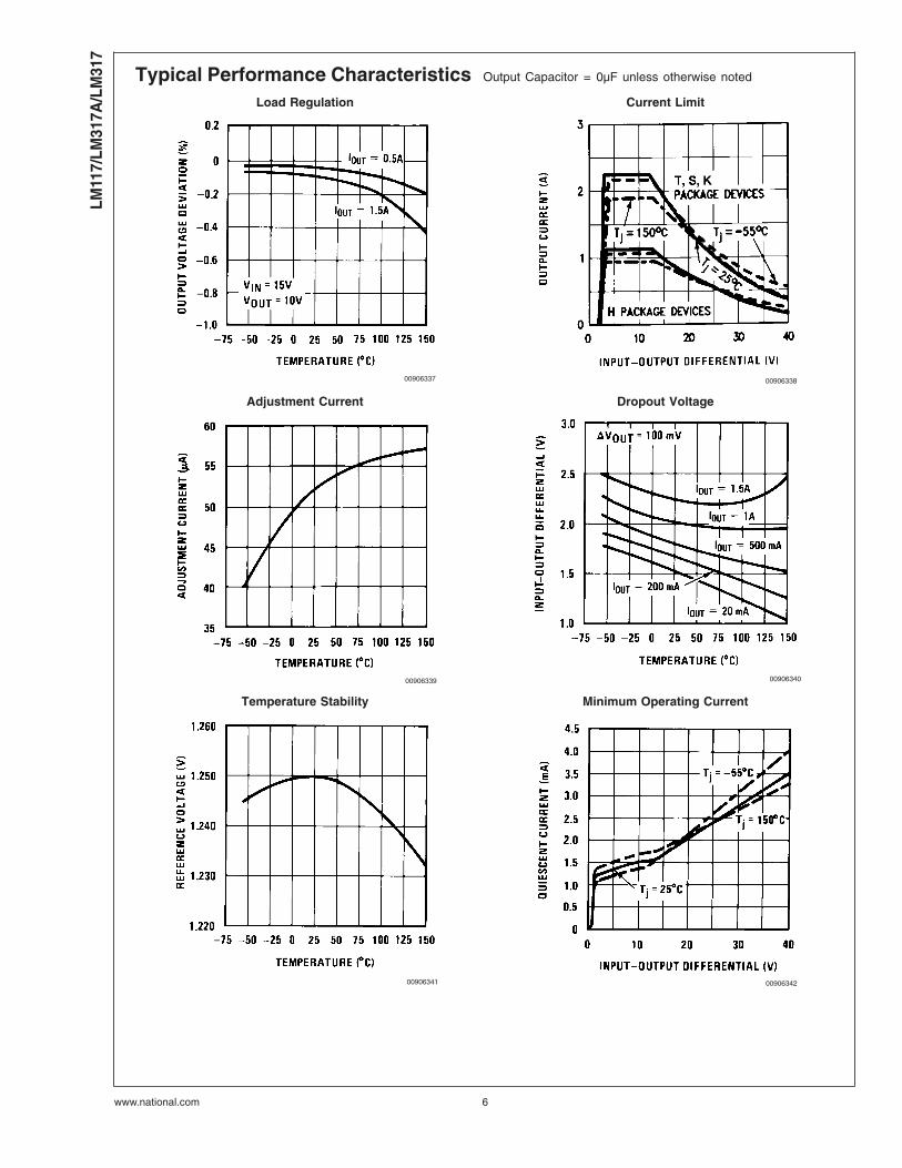
Typical Performance Characteristics Output Capacitor = 0µF unless otherwise noted
Load Regulation Current Limit
00906337 00906338
Adjustment Current Dropout Voltage
00906339 00906340
Temperature Stability Minimum Operating Current
00906341 00906342
LM11
7/LM
317A
/LM
317
www.national.com 6
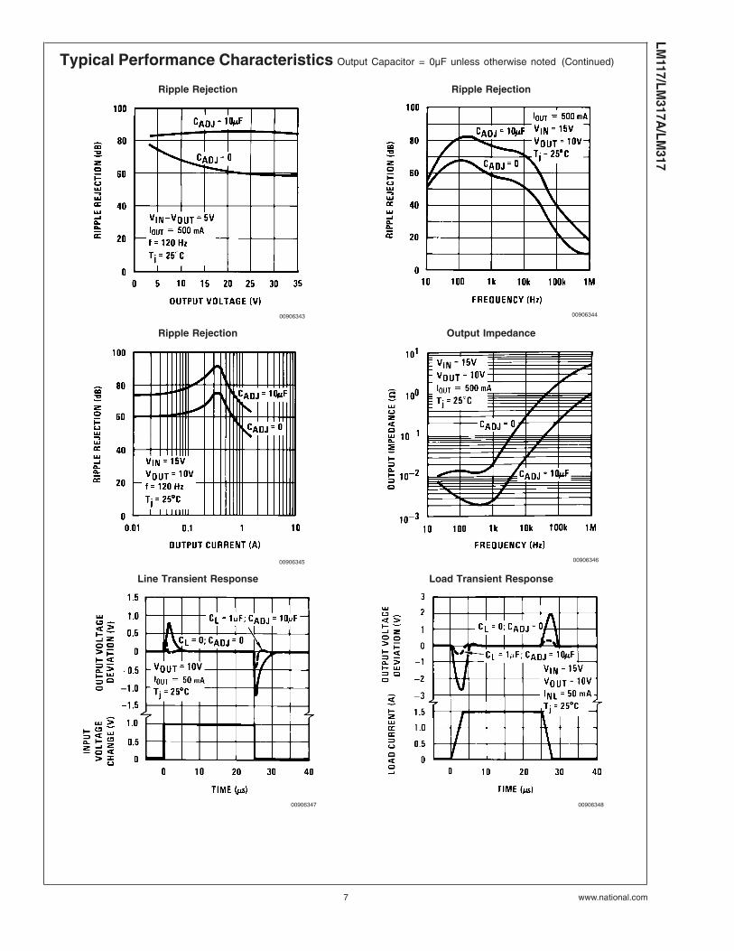
Typical Performance Characteristics Output Capacitor = 0µF unless otherwise noted (Continued)
Ripple Rejection Ripple Rejection
00906343 00906344
Ripple Rejection Output Impedance
00906345 00906346
Line Transient Response Load Transient Response
00906347 00906348
LM117/LM
317A/LM
317
www.national.com7
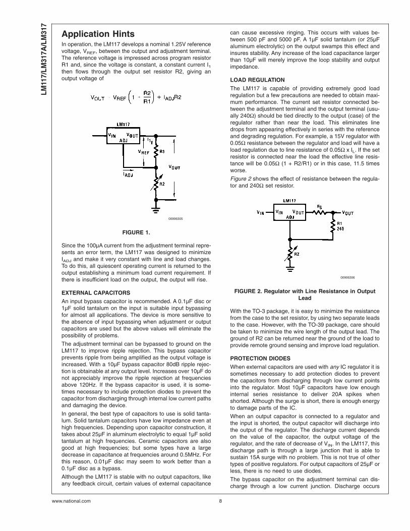
Application HintsIn operation, the LM117 develops a nominal 1.25V referencevoltage, VREF, between the output and adjustment terminal.The reference voltage is impressed across program resistorR1 and, since the voltage is constant, a constant current I1then flows through the output set resistor R2, giving anoutput voltage of
Since the 100µA current from the adjustment terminal repre-sents an error term, the LM117 was designed to minimizeIADJ and make it very constant with line and load changes.To do this, all quiescent operating current is returned to theoutput establishing a minimum load current requirement. Ifthere is insufficient load on the output, the output will rise.
EXTERNAL CAPACITORS
An input bypass capacitor is recommended. A 0.1µF disc or1µF solid tantalum on the input is suitable input bypassingfor almost all applications. The device is more sensitive tothe absence of input bypassing when adjustment or outputcapacitors are used but the above values will eliminate thepossibility of problems.
The adjustment terminal can be bypassed to ground on theLM117 to improve ripple rejection. This bypass capacitorprevents ripple from being amplified as the output voltage isincreased. With a 10µF bypass capacitor 80dB ripple rejec-tion is obtainable at any output level. Increases over 10µF donot appreciably improve the ripple rejection at frequenciesabove 120Hz. If the bypass capacitor is used, it is some-times necessary to include protection diodes to prevent thecapacitor from discharging through internal low current pathsand damaging the device.
In general, the best type of capacitors to use is solid tanta-lum. Solid tantalum capacitors have low impedance even athigh frequencies. Depending upon capacitor construction, ittakes about 25µF in aluminum electrolytic to equal 1µF solidtantalum at high frequencies. Ceramic capacitors are alsogood at high frequencies; but some types have a largedecrease in capacitance at frequencies around 0.5MHz. Forthis reason, 0.01µF disc may seem to work better than a0.1µF disc as a bypass.
Although the LM117 is stable with no output capacitors, likeany feedback circuit, certain values of external capacitance
can cause excessive ringing. This occurs with values be-tween 500 pF and 5000 pF. A 1µF solid tantalum (or 25µFaluminum electrolytic) on the output swamps this effect andinsures stability. Any increase of the load capacitance largerthan 10µF will merely improve the loop stability and outputimpedance.
LOAD REGULATION
The LM117 is capable of providing extremely good loadregulation but a few precautions are needed to obtain maxi-mum performance. The current set resistor connected be-tween the adjustment terminal and the output terminal (usu-ally 240Ω) should be tied directly to the output (case) of theregulator rather than near the load. This eliminates linedrops from appearing effectively in series with the referenceand degrading regulation. For example, a 15V regulator with0.05Ω resistance between the regulator and load will have aload regulation due to line resistance of 0.05Ω x IL. If the setresistor is connected near the load the effective line resis-tance will be 0.05Ω (1 + R2/R1) or in this case, 11.5 timesworse.
Figure 2 shows the effect of resistance between the regula-tor and 240Ω set resistor.
With the TO-3 package, it is easy to minimize the resistancefrom the case to the set resistor, by using two separate leadsto the case. However, with the TO-39 package, care shouldbe taken to minimize the wire length of the output lead. Theground of R2 can be returned near the ground of the load toprovide remote ground sensing and improve load regulation.
PROTECTION DIODES
When external capacitors are used with any IC regulator it issometimes necessary to add protection diodes to preventthe capacitors from discharging through low current pointsinto the regulator. Most 10µF capacitors have low enoughinternal series resistance to deliver 20A spikes whenshorted. Although the surge is short, there is enough energyto damage parts of the IC.
When an output capacitor is connected to a regulator andthe input is shorted, the output capacitor will discharge intothe output of the regulator. The discharge current dependson the value of the capacitor, the output voltage of theregulator, and the rate of decrease of VIN. In the LM117, thisdischarge path is through a large junction that is able tosustain 15A surge with no problem. This is not true of othertypes of positive regulators. For output capacitors of 25µF orless, there is no need to use diodes.
The bypass capacitor on the adjustment terminal can dis-charge through a low current junction. Discharge occurs
00906305
FIGURE 1.
00906306
FIGURE 2. Regulator with Line Resistance in OutputLead
LM11
7/LM
317A
/LM
317
www.national.com 8
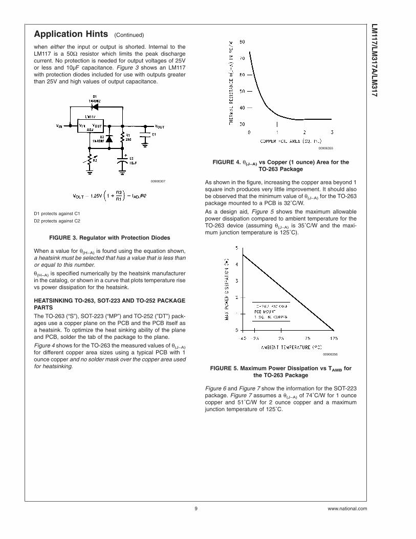
Application Hints (Continued)
when either the input or output is shorted. Internal to theLM117 is a 50Ω resistor which limits the peak dischargecurrent. No protection is needed for output voltages of 25Vor less and 10µF capacitance. Figure 3 shows an LM117with protection diodes included for use with outputs greaterthan 25V and high values of output capacitance.
When a value for θ(H−A) is found using the equation shown,a heatsink must be selected that has a value that is less thanor equal to this number.
θ(H−A) is specified numerically by the heatsink manufacturerin the catalog, or shown in a curve that plots temperature risevs power dissipation for the heatsink.
HEATSINKING TO-263, SOT-223 AND TO-252 PACKAGEPARTS
The TO-263 (“S”), SOT-223 (“MP”) and TO-252 (”DT”) pack-ages use a copper plane on the PCB and the PCB itself asa heatsink. To optimize the heat sinking ability of the planeand PCB, solder the tab of the package to the plane.
Figure 4 shows for the TO-263 the measured values of θ(J−A)
for different copper area sizes using a typical PCB with 1ounce copper and no solder mask over the copper area usedfor heatsinking.
As shown in the figure, increasing the copper area beyond 1square inch produces very little improvement. It should alsobe observed that the minimum value of θ(J−A) for the TO-263package mounted to a PCB is 32˚C/W.
As a design aid, Figure 5 shows the maximum allowablepower dissipation compared to ambient temperature for theTO-263 device (assuming θ(J−A) is 35˚C/W and the maxi-mum junction temperature is 125˚C).
Figure 6 and Figure 7 show the information for the SOT-223package. Figure 7 assumes a θ(J−A) of 74˚C/W for 1 ouncecopper and 51˚C/W for 2 ounce copper and a maximumjunction temperature of 125˚C.
00906307
D1 protects against C1
D2 protects against C2
FIGURE 3. Regulator with Protection Diodes
00906355
FIGURE 4. θ(J−A) vs Copper (1 ounce) Area for theTO-263 Package
00906356
FIGURE 5. Maximum Power Dissipation vs TAMB forthe TO-263 Package
LM117/LM
317A/LM
317
www.national.com9
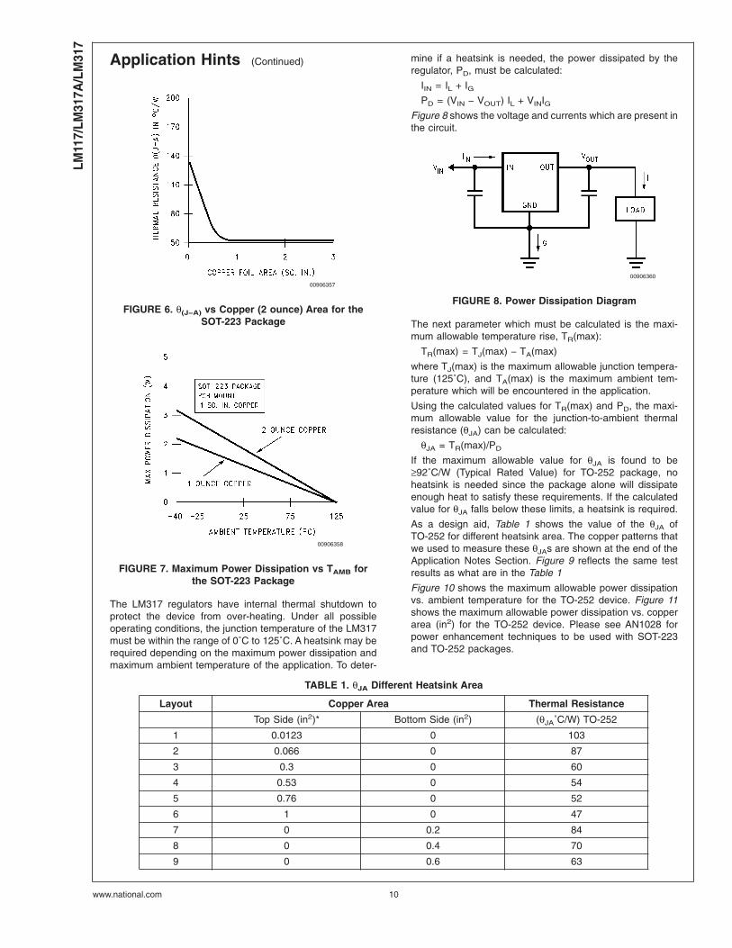
Application Hints (Continued)
The LM317 regulators have internal thermal shutdown toprotect the device from over-heating. Under all possibleoperating conditions, the junction temperature of the LM317must be within the range of 0˚C to 125˚C. A heatsink may berequired depending on the maximum power dissipation andmaximum ambient temperature of the application. To deter-
mine if a heatsink is needed, the power dissipated by theregulator, PD, must be calculated:
IIN = IL + IGPD = (VIN − VOUT) IL + VINIG
Figure 8 shows the voltage and currents which are present inthe circuit.
The next parameter which must be calculated is the maxi-mum allowable temperature rise, TR(max):
TR(max) = TJ(max) − TA(max)
where TJ(max) is the maximum allowable junction tempera-ture (125˚C), and TA(max) is the maximum ambient tem-perature which will be encountered in the application.
Using the calculated values for TR(max) and PD, the maxi-mum allowable value for the junction-to-ambient thermalresistance (θJA) can be calculated:
θJA = TR(max)/PD
If the maximum allowable value for θJA is found to be≥92˚C/W (Typical Rated Value) for TO-252 package, noheatsink is needed since the package alone will dissipateenough heat to satisfy these requirements. If the calculatedvalue for θJA falls below these limits, a heatsink is required.
As a design aid, Table 1 shows the value of the θJA ofTO-252 for different heatsink area. The copper patterns thatwe used to measure these θJAs are shown at the end of theApplication Notes Section. Figure 9 reflects the same testresults as what are in the Table 1
Figure 10 shows the maximum allowable power dissipationvs. ambient temperature for the TO-252 device. Figure 11shows the maximum allowable power dissipation vs. copperarea (in2) for the TO-252 device. Please see AN1028 forpower enhancement techniques to be used with SOT-223and TO-252 packages.
TABLE 1. θJA Different Heatsink Area
Layout Copper Area Thermal Resistance
Top Side (in2)* Bottom Side (in2) (θJA˚C/W) TO-252
1 0.0123 0 103
2 0.066 0 87
3 0.3 0 60
4 0.53 0 54
5 0.76 0 52
6 1 0 47
7 0 0.2 84
8 0 0.4 70
9 0 0.6 63
00906357
FIGURE 6. θ(J−A) vs Copper (2 ounce) Area for theSOT-223 Package
00906358
FIGURE 7. Maximum Power Dissipation vs TAMB forthe SOT-223 Package
00906360
FIGURE 8. Power Dissipation Diagram
LM11
7/LM
317A
/LM
317
www.national.com 10
Application Hints (Continued)
TABLE 1. θJA Different Heatsink Area (Continued)
Layout Copper Area Thermal Resistance
10 0 0.8 57
11 0 1 57
12 0.066 0.066 89
13 0.175 0.175 72
14 0.284 0.284 61
15 0.392 0.392 55
16 0.5 0.5 53
Note: * Tab of device attached to topside of copper.
00906361
FIGURE 9. θJA vs 2oz Copper Area for TO-252
00906363
FIGURE 10. Maximum Allowable Power Dissipation vs. Ambient Temperature for TO-252
LM117/LM
317A/LM
317
www.national.com11
Application Hints (Continued)
00906362
FIGURE 11. Maximum Allowable Power Dissipation vs. 2oz Copper Area for TO-252
00906364
FIGURE 12. Top View of the Thermal Test Pattern in Actual Scale
LM11
7/LM
317A
/LM
317
www.national.com 12
Application Hints (Continued)
00906365
FIGURE 13. Bottom View of the Thermal Test Pattern in Actual Scale
LM117/LM
317A/LM
317
www.national.com13
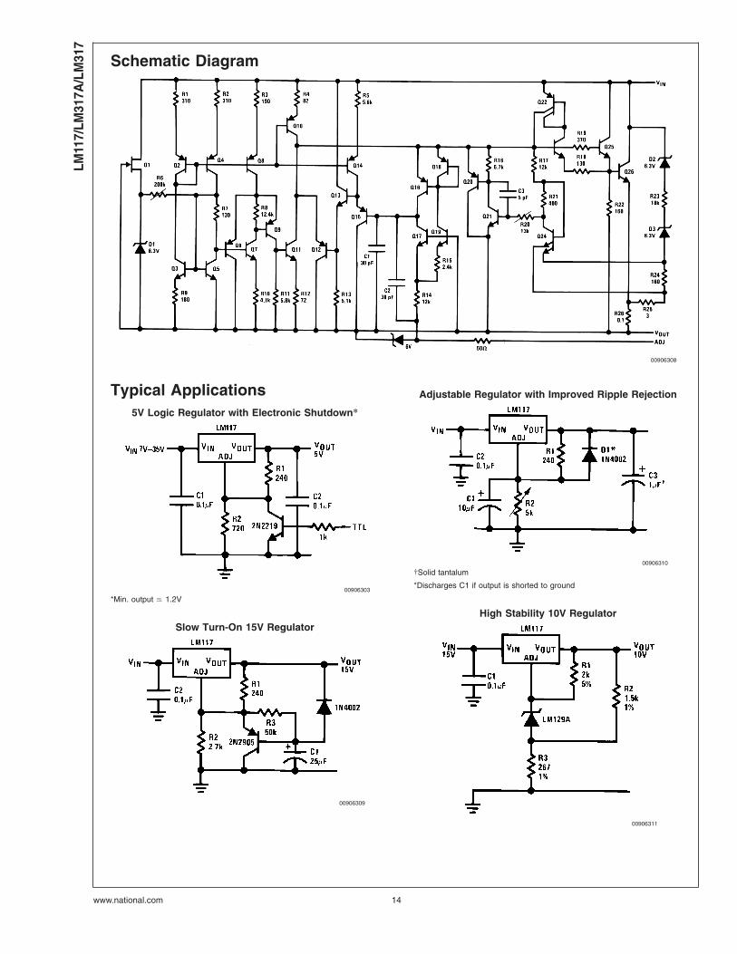
Schematic Diagram
00906308
Typical Applications5V Logic Regulator with Electronic Shutdown*
00906303
*Min. output ) 1.2V
Slow Turn-On 15V Regulator
00906309
Adjustable Regulator with Improved Ripple Rejection
00906310
†Solid tantalum
*Discharges C1 if output is shorted to ground
High Stability 10V Regulator
00906311
LM11
7/LM
317A
/LM
317
www.national.com 14
Typical Applications (Continued)
High Current Adjustable Regulator
00906312
‡Optional — improves ripple rejection
†Solid tantalum
*Minimum load current = 30 mA
0 to 30V Regulator
00906313
Full output current not available at high input-output voltages
Power Follower
00906314
LM117/LM
317A/LM
317
www.national.com15
Typical Applications (Continued)
5A Constant Voltage/Constant Current Regulator
00906315
†Solid tantalum
*Lights in constant current mode
1A Current Regulator
00906316
1.2V–20V Regulator with Minimum Program Current
00906317
*Minimum load current ) 4 mA
High Gain Amplifier
00906318
LM11
7/LM
317A
/LM
317
www.national.com 16
Typical Applications (Continued)
Low Cost 3A Switching Regulator
00906319
†Solid tantalum
*Core — Arnold A-254168-2 60 turns
4A Switching Regulator with Overload Protection
00906320
†Solid tantalum
*Core — Arnold A-254168-2 60 turns
Precision Current Limiter
00906321
LM117/LM
317A/LM
317
www.national.com17
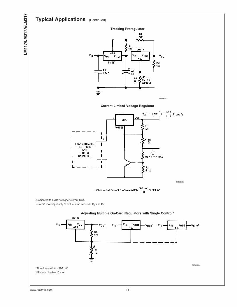
Typical Applications (Continued)
Tracking Preregulator
00906322
Current Limited Voltage Regulator
00906323
(Compared to LM117’s higher current limit)
— At 50 mA output only 3⁄4 volt of drop occurs in R3 and R4
Adjusting Multiple On-Card Regulators with Single Control*
00906324
*All outputs within ±100 mV
†Minimum load — 10 mA
LM11
7/LM
317A
/LM
317
www.national.com 18
Typical Applications (Continued)
AC Voltage Regulator
00906325
12V Battery Charger
00906326
Use of RS allows low charging rates with fully charged battery.
50mA Constant Current Battery Charger
00906327
LM117/LM
317A/LM
317
www.national.com19
Typical Applications (Continued)
Adjustable 4A Regulator
00906328
Current Limited 6V Charger
00906329
*Sets peak current (0.6A for 1Ω)
**The 1000µF is recommended to filter out input transients
Digitally Selected Outputs
00906302
*Sets maximum VOUT
LM11
7/LM
317A
/LM
317
www.national.com 20
Physical Dimensions inches (millimeters)unless otherwise noted
TO-3 Metal Can Package (K)NS Package Number K02A
TO-3 Metal Can Package (K)Mil-Aero Product
NS Package Number K02C
LM117/LM
317A/LM
317
www.national.com21
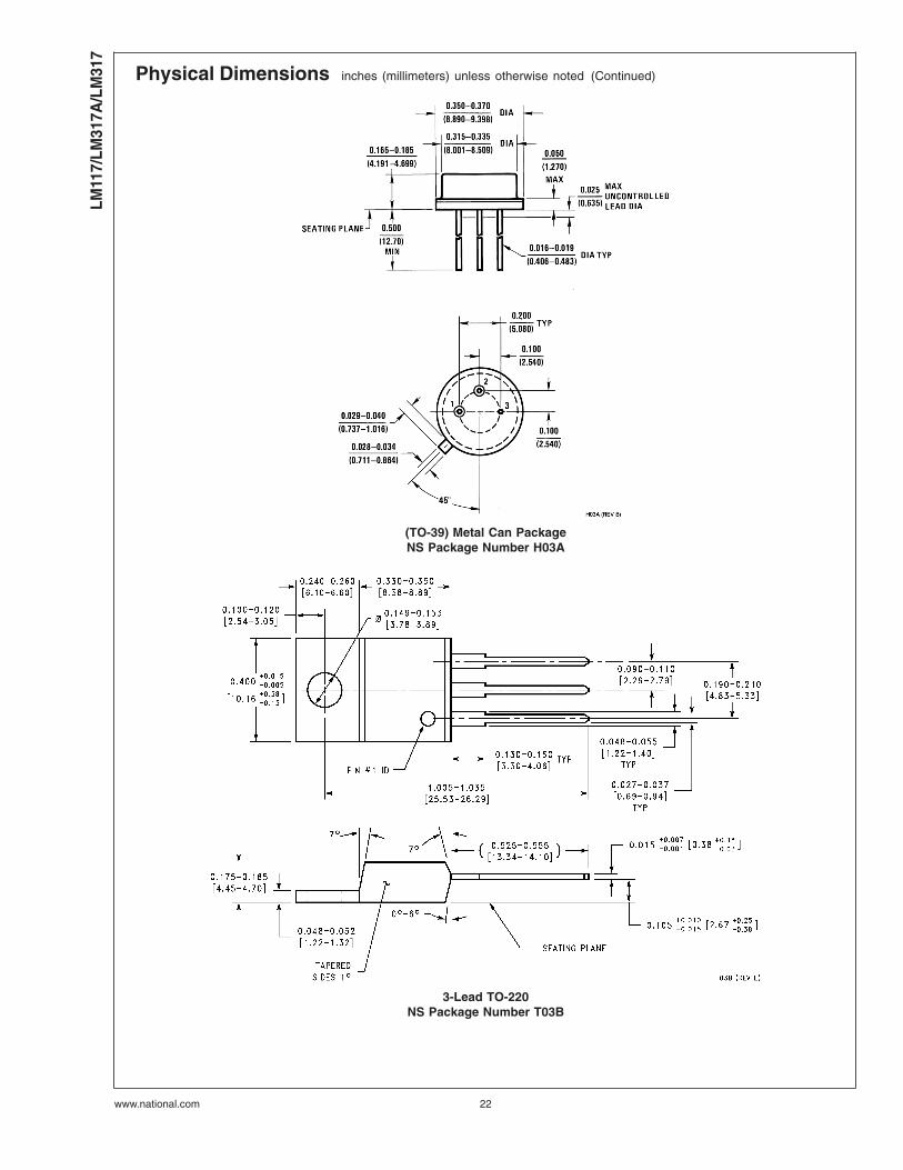
Physical Dimensions inches (millimeters) unless otherwise noted (Continued)
(TO-39) Metal Can PackageNS Package Number H03A
3-Lead TO-220NS Package Number T03B
LM11
7/LM
317A
/LM
317
www.national.com 22
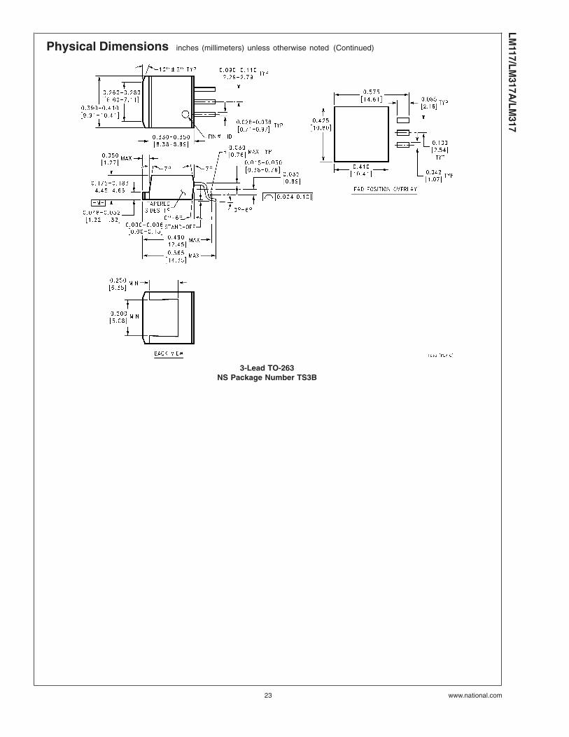
Physical Dimensions inches (millimeters) unless otherwise noted (Continued)
3-Lead TO-263NS Package Number TS3B
LM117/LM
317A/LM
317
www.national.com23
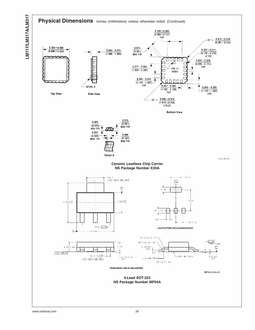
Physical Dimensions inches (millimeters) unless otherwise noted (Continued)
Ceramic Leadless Chip CarrierNS Package Number E20A
4-Lead SOT-223NS Package Number MP04A
LM11
7/LM
317A
/LM
317
www.national.com 24
Physical Dimensions inches (millimeters) unless otherwise noted (Continued)
3-Lead D-PackNS Package Number TD03B
LIFE SUPPORT POLICY
NATIONAL’S PRODUCTS ARE NOT AUTHORIZED FOR USE AS CRITICAL COMPONENTS IN LIFE SUPPORTDEVICES OR SYSTEMS WITHOUT THE EXPRESS WRITTEN APPROVAL OF THE PRESIDENT AND GENERALCOUNSEL OF NATIONAL SEMICONDUCTOR CORPORATION. As used herein:
1. Life support devices or systems are devices orsystems which, (a) are intended for surgical implantinto the body, or (b) support or sustain life, andwhose failure to perform when properly used inaccordance with instructions for use provided in thelabeling, can be reasonably expected to result in asignificant injury to the user.
2. A critical component is any component of a lifesupport device or system whose failure to performcan be reasonably expected to cause the failure ofthe life support device or system, or to affect itssafety or effectiveness.
BANNED SUBSTANCE COMPLIANCE
National Semiconductor certifies that the products and packing materials meet the provisions of the Customer ProductsStewardship Specification (CSP-9-111C2) and the Banned Substances and Materials of Interest Specification(CSP-9-111S2) and contain no ‘‘Banned Substances’’ as defined in CSP-9-111S2.
National SemiconductorAmericas CustomerSupport CenterEmail: [email protected]: 1-800-272-9959
National SemiconductorEurope Customer Support Center
Fax: +49 (0) 180-530 85 86Email: [email protected]
Deutsch Tel: +49 (0) 69 9508 6208English Tel: +44 (0) 870 24 0 2171Français Tel: +33 (0) 1 41 91 8790
National SemiconductorAsia Pacific CustomerSupport CenterEmail: [email protected]
National SemiconductorJapan Customer Support CenterFax: 81-3-5639-7507Email: [email protected]: 81-3-5639-7560
www.national.com
LM117/LM
317A/LM
3173-Term
inalAdjustable
Regulator
National does not assume any responsibility for use of any circuitry described, no circuit patent licenses are implied and National reserves the right at any time without notice to change said circuitry and specifications.

This datasheet has been download from:
www.datasheetcatalog.com
Datasheets for electronics components.
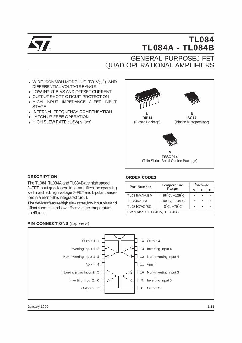
GENERAL PURPOSEJ-FETQUAD OPERATIONAL AMPLIFIERS
.WIDE COMMON-MODE (UP TO VCC+) AND
DIFFERENTIAL VOLTAGE RANGE. LOW INPUT BIAS AND OFFSET CURRENT.OUTPUT SHORT-CIRCUIT PROTECTION.HIGH INPUT IMPEDANCE J–FET INPUTSTAGE. INTERNAL FREQUENCY COMPENSATION. LATCH UP FREE OPERATION.HIGH SLEW RATE : 16V/µs (typ)
NDIP14
(Plastic Package)
Inverting Input 2
Non-inverting Input 2
Non-inverting Input 1
CCV -CCV
1
2
3
4
8
5
6
7
9
10
11
12
13
14
+
Output 3
Output 4
Non-inverting Input 4
Inverting Input 4
Non-inverting Input 3
Inverting Input 3
-
+
-
+
-
+
-
+
Output 1
Inverting Input 1
Output 2
PIN CONNECTIONS (top view)
DESCRIPTION
The TL084, TL084A and TL084B are high speedJ–FET input quad operationalamplifiers incorporatingwell matched,high voltageJ–FETand bipolar transis-tors in a monolithic integratedcircuit.The devicesfeaturehighslew rates, low inputbiasandoffsetcurrents, and low offset voltage temperaturecoefficient.
DSO14
(Plastic Micropackage)
TL084TL084A - TL084B
January 1999
ORDER CODES
Part Number TemperatureRange
Package
N D P
TL084M/AM/BM –55oC, +125oC • • •TL084I/AI/BI –40oC, +105oC • • •TL084C/AC/BC 0oC, +70oC • • •Examples : TL084CN, TL084CD
PTSSOP14
(Thin Shrink Small Outline Package)
1/11
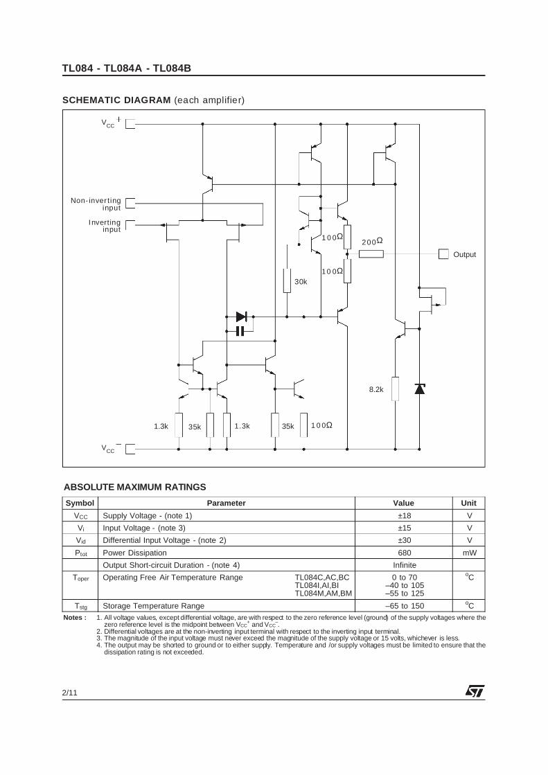
ABSOLUTE MAXIMUM RATINGS
Symbol Parameter Value Unit
VCC Supply Voltage - (note 1) ±18 V
Vi Input Voltage - (note 3) ±15 V
Vid Differential Input Voltage - (note 2) ±30 V
Ptot Power Dissipation 680 mW
Output Short-circuit Duration - (note 4) Infinite
Toper Operating Free Air Temperature Range TL084C,AC,BCTL084I,AI,BITL084M,AM,BM
0 to 70–40 to 105–55 to 125
oC
Tstg Storage Temperature Range –65 to 150 oCNotes : 1. All voltage values, except differential voltage, are with respect to the zero reference level (ground) of the supply voltages where the
zero reference level is the midpoint between VCC+ and VCC
–.2. Differential voltages are at the non-inverting input terminal with respect to the inverting input terminal.3. The magnitude of the input voltage must never exceed the magnitude of the supply voltage or 15 volts, whichever is less.4. The output may be shorted to ground or to either supply. Temperature and /or supply voltages must be limited to ensure that the
dissipation rating is not exceeded.
Output
Non- inver tinginput
Invertinginput
VCC
VCC
200ΩΩ1 0 0
Ω10 0
1.3k
30k
35k 35k Ω1 0 01.3k
8.2k
SCHEMATIC DIAGRAM (each amplifier)
TL084 - TL084A - TL084B
2/11
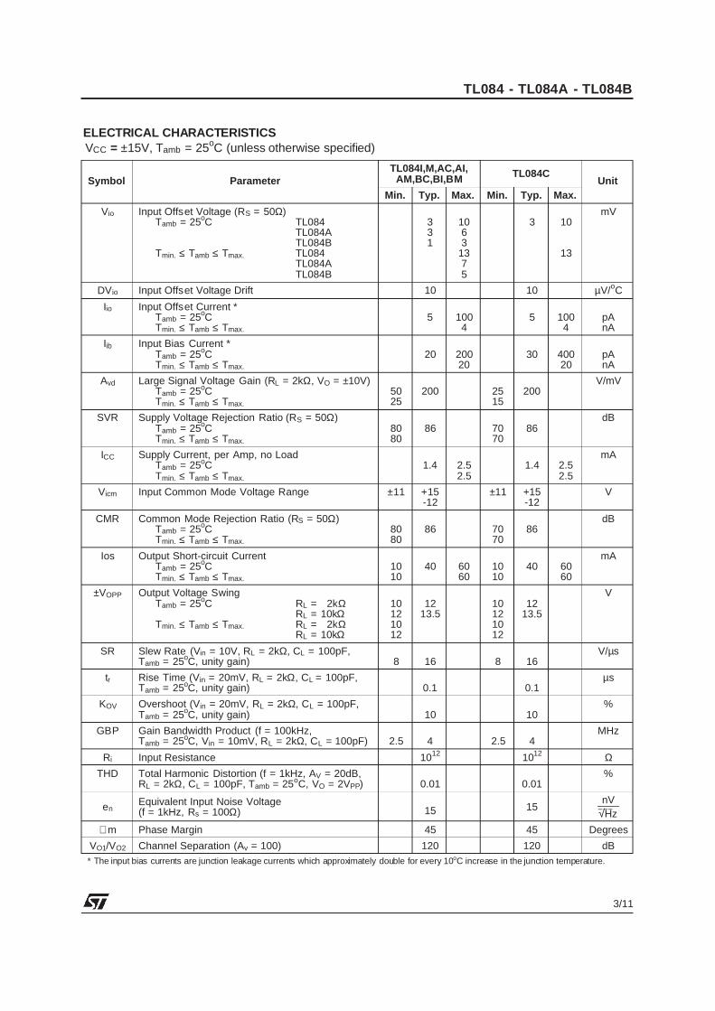
ELECTRICAL CHARACTERISTICSVCC = ±15V, Tamb = 25oC (unless otherwise specified)
Symbol ParameterTL084I,M,AC,AI,
AM,BC,BI,BM TL084CUnit
Min. Typ. Max. Min. Typ. Max.
Vio Input Offset Voltage (RS = 50Ω)Tamb = 25oC TL084
TL084ATL084B
Tmin. ≤ Tamb ≤ Tmax. TL084TL084ATL084B
331
1063
1375
3 10
13
mV
DVio Input Offset Voltage Drift 10 10 µV/oC
Iio Input Offset Current *Tamb = 25oCTmin. ≤ Tamb ≤ Tmax.
5 1004
5 1004
pAnA
Iib Input Bias Current *Tamb = 25oCTmin. ≤ Tamb ≤ Tmax.
20 20020
30 40020
pAnA
Avd Large Signal Voltage Gain (RL = 2kΩ, VO = ±10V)Tamb = 25oCTmin. ≤ Tamb ≤ Tmax.
5025
200 2515
200V/mV
SVR Supply Voltage Rejection Ratio (RS = 50Ω)Tamb = 25oCTmin. ≤ Tamb ≤ Tmax.
8080
86 7070
86dB
ICC Supply Current, per Amp, no LoadTamb = 25oCTmin. ≤ Tamb ≤ Tmax.
1.4 2.52.5
1.4 2.52.5
mA
Vicm Input Common Mode Voltage Range ±11 +15-12
±11 +15-12
V
CMR Common Mode Rejection Ratio (RS = 50Ω)Tamb = 25oCTmin. ≤ Tamb ≤ Tmax.
8080
86 7070
86dB
Ios Output Short-circuit CurrentTamb = 25oCTmin. ≤ Tamb ≤ Tmax.
1010
40 6060
1010
40 6060
mA
±VOPP Output Voltage SwingTamb = 25oC RL = 2kΩ
RL = 10kΩTmin. ≤ Tamb ≤ Tmax. RL = 2kΩ
RL = 10kΩ
10121012
1213.5
10121012
1213.5
V
SR Slew Rate (Vin = 10V, RL = 2kΩ, CL = 100pF,Tamb = 25oC, unity gain) 8 16 8 16
V/µs
tr Rise Time (Vin = 20mV, RL = 2kΩ, CL = 100pF,Tamb = 25oC, unity gain) 0.1 0.1
µs
KOV Overshoot (Vin = 20mV, RL = 2kΩ, CL = 100pF,Tamb = 25oC, unity gain) 10 10
%
GBP Gain Bandwidth Product (f = 100kHz,Tamb = 25oC, Vin = 10mV, RL = 2kΩ, CL = 100pF) 2.5 4 2.5 4
MHz
Ri Input Resistance 1012 1012 ΩTHD Total Harmonic Distortion (f = 1kHz, AV = 20dB,
RL = 2kΩ, CL = 100pF, Tamb = 25oC, VO = 2VPP) 0.01 0.01%
enEquivalent Input Noise Voltage(f = 1kHz, Rs = 100Ω) 15 15
nV√Hz
∅ m Phase Margin 45 45 Degrees
VO1/VO2 Channel Separation (Av = 100) 120 120 dB* The input bias currents are junction leakage currents which approximately double for every 10oC increase in the junction temperature.
TL084 - TL084A - TL084B
3/11
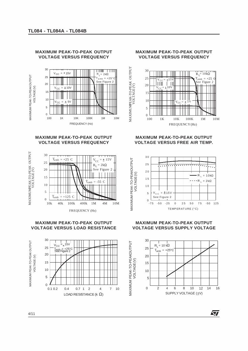
30
20
25
15
10
5
0
MA
XIM
UM
PE
AK
-TO
-PE
AK
OU
TP
UT
VO
LTA
GE
(V)
100 1K 10K 100K 10M1M
FREQUENCY (Hz)
See Figure 2
= 2kΩRL
= +25° CT a m b
= 15VV CC
= 5VVCC
= 10VVCC
MAXIMUM PEAK-TO-PEAK OUTPUTVOLTAGE VERSUS FREQUENCY
30
20
25
15
10
5
0
MA
XIM
UM
PE
AK
-TO
-PE
AK
OU
TP
UT
VO
LTA
GE
(V)
100 1K 10K 100K 10M1M
FREQUENCY(Hz)
See Figure 2= +25 CTamb
= 10kΩRL
VCC= 10V
VCC= 15V
VCC = 5V
MAXIMUM PEAK-TO-PEAK OUTPUTVOLTAGE VERSUS FREQUENCY
30
25
20
15
10
5
0
MA
XIM
UM
PE
AK
-TO
-PE
AK
OU
TP
UT
VO
LTA
GE
(V)
FREQUENCY (Hz)
10k 40k 100k 400k 1M 4M 10M
Ta mb = +25 C
Ta mb = -55 C
Ta mb = +125 C
RL = 2kΩSee Figure 2
VCC= 15V
MAXIMUM PEAK-TO-PEAK OUTPUTVOLTAGE VERSUS FREQUENCY
3 0
2 5
2 0
1 0
5
1 5
0-7 5 - 25 2 5 7 5 125-5 0 0 5 0 -50
MA
XIM
UM
PE
AK
-TO
-PE
AK
OU
TP
UT
VO
LTA
GE
(V)
TEMP ER AT URE (° C)
V C C = 15 V
See Figure 2
R L = 10kΩ
R L = 2kΩ
MAXIMUM PEAK-TO-PEAK OUTPUTVOLTAGE VERSUS FREE AIR TEMP.
30
25
20
15
10
5
0MA
XIM
UM
PE
AK
-TO
-PE
AK
OU
TP
UT
VO
LTA
GE
(V)
0.1 0.2 0.4 0.7 1 2 4 7 10
Tamb = +25°CVCC
= 15V
See Figure 2
LOAD RESISTANCE (k Ω)
MAXIMUM PEAK-TO-PEAK OUTPUTVOLTAGE VERSUS LOAD RESISTANCE
30
25
20
15
10
5
0 2 4 6 8 10 12 14 16
MA
XIM
UM
PE
AK
-TO
-PE
AKO
UT
PU
TV
OLT
AG
E(V
)
RL = 10 kΩTamb = +25°C
SUPPLY VOLTAGE ( V)
MAXIMUM PEAK-TO-PEAK OUTPUTVOLTAGE VERSUS SUPPLY VOLTAGE
TL084 - TL084A - TL084B
4/11
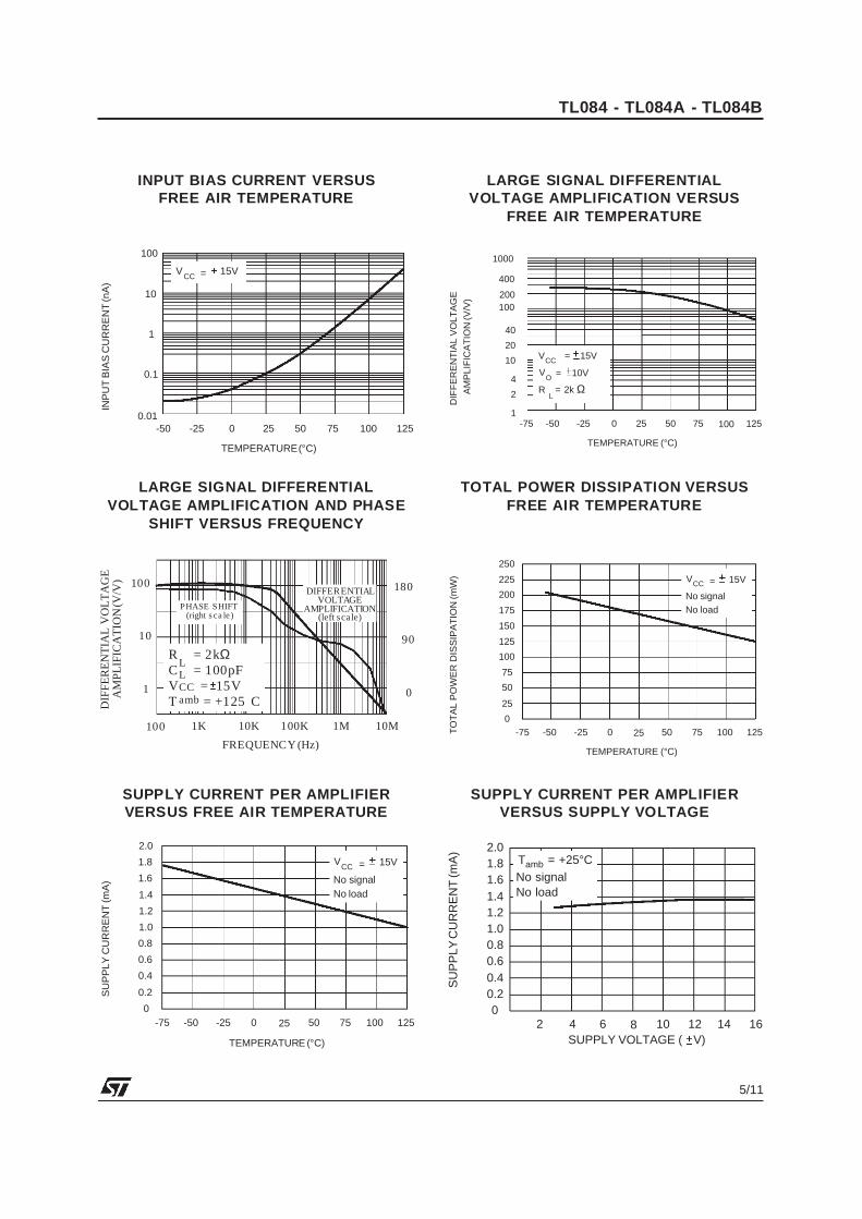
100
10
1
0.1
0.01
INP
UT
BIA
SC
UR
RE
NT
(nA
)
-50 -25 0 25 50 75 100 125
TEMPERATURE(°C)
VCC = 15V
INPUT BIAS CURRENT VERSUSFREE AIR TEMPERATURE
1000
400
200100
20
40
10
4
2
1
DIF
FE
RE
NT
IAL
VO
LTA
GE
AM
PLI
FIC
AT
ION
(V/V
)
-75 -50 -25 0 25 50 75 100 125
TEMPERATURE (°C)
RL
= 2k ΩV
O = 10V
VCC = 15V
LARGE SIGNAL DIFFERENTIALVOLTAGE AMPLIFICATION VERSUS
FREE AIR TEMPERATURE
FREQUENCY(Hz)
DIF
FE
RE
NT
IAL
VO
LTA
GE
AM
PLI
FIC
AT
ION
(V/V
) 100
10
100 1K 10K 100K 10M1M
1
DIFFERENTIALVOLTAGE
AMPLIFICATION(left scale)
180
90
0
R = 2kΩC = 100pFV = 15VT = +125 C
LLCCamb
PHASE SHIFT(right s ca le)
LARGE SIGNAL DIFFERENTIALVOLTAGE AMPLIFICATION AND PHASE
SHIFT VERSUS FREQUENCY
250
225
200
175
150
125
100
75
50
25
0
TO
TA
LP
OW
ER
DIS
SIP
AT
ION
(mW
)
-75 -50 -25 0 25 50 75 100 125
TEMPERATURE (°C)
VCC = 15V
No signalNo load
TOTAL POWER DISSIPATION VERSUSFREE AIR TEMPERATURE
2.0
1.8
1.6
1.4
1.2
1.0
0.8
0.6
0.4
0.2
0
SU
PP
LYC
UR
RE
NT
(mA
)
-75 -50 -25 0 25 50 75 100 125
TEMPERATURE (°C)
VCC = 15V
No signalNo load
SUPPLY CURRENT PER AMPLIFIERVERSUS FREE AIR TEMPERATURE
2.01.81.61.41.21.00.80.60.40.20
SU
PP
LYC
UR
RE
NT
(mA
)
2 4 6 8 10 12 14 16
No signalNo load
= +25°CTamb
SUPPLY VOLTAGE ( V)
SUPPLY CURRENT PER AMPLIFIERVERSUS SUPPLY VOLTAGE
TL084 - TL084A - TL084B
5/11
89
88
87
86
85
84
-50 -25 0 25 50 75 100 125
CO
MM
ON
MO
DE
MO
DE
RE
JEC
TIO
N
RA
TIO
(dB
)
TEMPERATURE (°C)
83-75
RL = 10 kΩ
= 15VVC C
COMMON MODE REJECTION RATIOVERSUS FREE AIR TEMPERATURE
6
4
2
0
-2
-4
0 0.5 1 1.5 2 2.5 3 3.5INP
UT
AN
DO
UT
PU
TV
OLT
AG
ES
(V)
TIME (µs)
-6
= 15VVCCRL = 2 kΩ
= 100pFCLTamb= +25 C
OUTPUTINPUT
VOLTAGE FOLLOWER LARGE SIGNALPULSE RESPONSE
t r
28
24
20
16
12
8
4
0
-4
OU
TP
UT
VO
LTA
GE
(mV
)
0 0.1 0.2 0.3 0.4 0.5 0.6 0.7
TIME ( µs)
10%
90%
OVERSHOOT
R L = 2k ΩTamb = +25°C
VCC
= 15V
OUTPUT VOLTAGE VERSUSELAPSED TIME
70
60
50
40
30
20
10
0
EQ
UIV
ALE
NT
INP
UT
NO
ISE
VO
LTA
GE
(nV
/VH
z)
10 40 100 400 1k 4k 10k 40k 100k
FREQUENCY (Hz)
A V = 10
R S = 100 ΩTamb = +25°C
VCC = 15V
EQUIVALENT INPUT NOISE VOLTAGEVERSUS FREQUENCY
1
0.4
0.1
0.04
0.01
0.004
0.001TO
TA
LH
AR
MO
NIC
DIS
TO
RT
ION
(%)
100 400 1k 4k 10k 40k 100k
FREQUENCY (Hz)
A V = 1
T amb = +25°C
VCC = 15V
= 6VV O (rms)
A V = 1
Tamb = +25°C
= 6VV O (rms)
V CC = 15V
TOTAL HARMONIC DISTORTION VERSUSFREQUENCY
TL084 - TL084A - TL084B
6/11
-
eI
TL0841/4
eo
CL= 100pF R = 2kΩL
Figure 1 : Voltage Follower
PARAMETER MEASUREMENT INFORMATION
-eI
TL084
RL
1/4
CL= 100pF
1k Ω
10k Ω
eo
Figure 2 : Gain-of-10 Inverting Amplifier
-
TL084
1/4
-
-
-
TL084
1/4
TL084
1/4
TL084
1/4
1M Ω
1µF
Output A
Output B
Output C
Input
100k Ω 100k Ω100k Ω
100k Ω1OO µF
VCC+
f = 100kHzO
TYPICAL APPLICATIONS
AUDIO DISTRIBUTION AMPLIFIER
TL084 - TL084A - TL084B
7/11
-
-TL08 4
1/422 0pF
43 k ΩInput
1 .5k Ω
43k Ω
22 0p F
43 k Ω
16 k Ω
TL08 4
1/4
30 k Ω
Output A
-
TL08 4
1/4
1 .5k Ω
22 0p F
43 k Ω
220pF
43 k Ω
-
TL 084
1/4
43 k Ω
16 k Ω
30 k Ω
Output B
Ground
TYPICAL APPLICATIONS (continued)
POSITIVE FEEDBACK BANDPASS FILTER
CASCADED BANDPASS FILTERfo = 100kHz ; Q = 69 ; Gain = 16
OUTPUT B
SECOND ORDER BANDPASS FILTERfo = 100kHz ; Q = 30 ; Gain = 4
OUTPUT A
TL084 - TL084A - TL084B
8/11
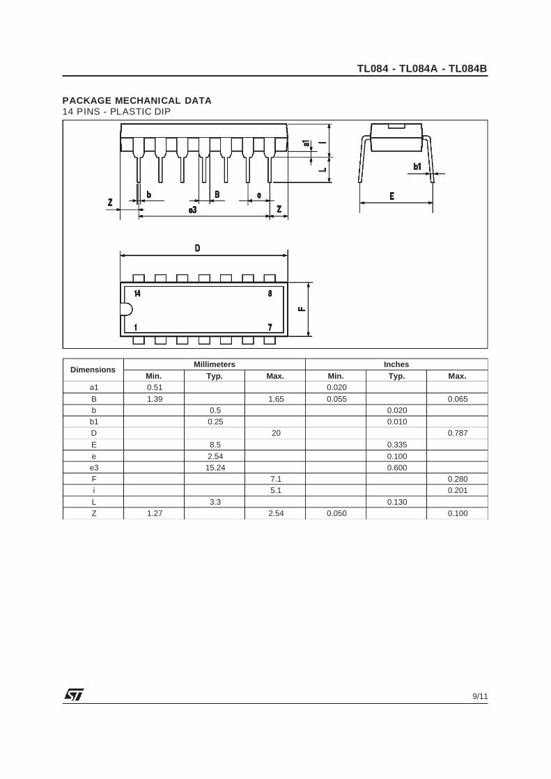
PACKAGE MECHANICAL DATA14 PINS - PLASTIC DIP
DimensionsMillimeters Inches
Min. Typ. Max. Min. Typ. Max.a1 0.51 0.020
B 1.39 1.65 0.055 0.065b 0.5 0.020b1 0.25 0.010D 20 0.787
E 8.5 0.335
e 2.54 0.100e3 15.24 0.600F 7.1 0.280i 5.1 0.201
L 3.3 0.130Z 1.27 2.54 0.050 0.100
TL084 - TL084A - TL084B
9/11
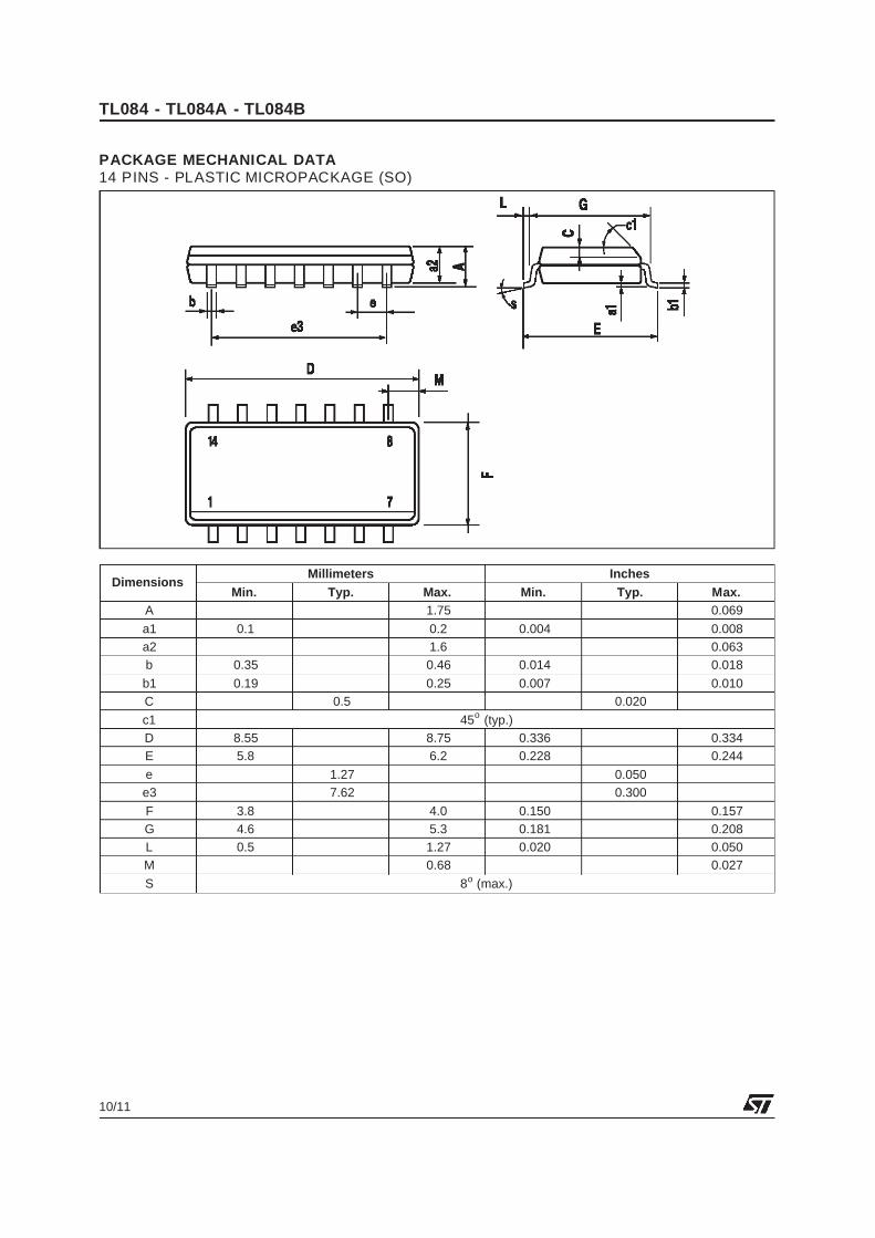
PACKAGE MECHANICAL DATA14 PINS - PLASTIC MICROPACKAGE (SO)
DimensionsMillimeters Inches
Min. Typ. Max. Min. Typ. Max.A 1.75 0.069
a1 0.1 0.2 0.004 0.008a2 1.6 0.063b 0.35 0.46 0.014 0.018
b1 0.19 0.25 0.007 0.010C 0.5 0.020
c1 45o (typ.)D 8.55 8.75 0.336 0.334E 5.8 6.2 0.228 0.244
e 1.27 0.050e3 7.62 0.300
F 3.8 4.0 0.150 0.157G 4.6 5.3 0.181 0.208L 0.5 1.27 0.020 0.050M 0.68 0.027
S 8o (max.)
TL084 - TL084A - TL084B
10/11
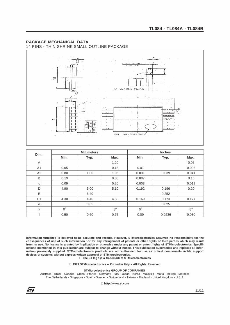
PACKAGE MECHANICAL DATA14 PINS - THIN SHRINK SMALL OUTLINE PACKAGE
Dim.Millimeters Inches
Min. Typ. Max. Min. Typ. Max.
A 1.20 0.05
A1 0.05 0.15 0.01 0.006
A2 0.80 1.00 1.05 0.031 0.039 0.041
b 0.19 0.30 0.007 0.15
c 0.09 0.20 0.003 0.012
D 4.90 5.00 5.10 0.192 0.196 0.20
E 6.40 0.252
E1 4.30 4.40 4.50 0.169 0.173 0.177
e 0.65 0.025
k 0o 8o 0o 8o
l 0.50 0.60 0.75 0.09 0.0236 0.030
Information furnished is believed to be accurate and reliable. However, STMicroelectronics assumes no responsibility for theconsequences of use of such information nor for any infringement of patents or other rights of third parties which may resultfrom its use. No license is granted by implication or otherwise under any patent or patent rights of STMicroelectronics. Specifi-cations mentioned in this publication are subject to change without notice. This publication supersedes and replaces all infor-mation previously supplied. STMicroelectronics products are not authorized for use as critical components in life supportdevices or systems without express written approval of STMicroelectronics.
The ST logo is a trademark of STMicroelectronics
1999 STMicroelectronics – Printed in Italy – All Rights Reserved
STMicroelectronics GROUP OF COMPANIESAustralia - Brazil - Canada - China - France - Germany - Italy - Japan - Korea - Malaysia - Malta - Mexico - Morocco
The Netherlands - Singapore - Spain - Sweden - Switzerland - Taiwan - Thailand - United Kingdom - U.S.A.
http://www.st.com
TL084 - TL084A - TL084B
11/11