automating the layout of reconfigurable subsystems via template reduction
TRANSCRIPT
Automating the Layout of Reconfigurable Subsystems Using Circuit Generators
Shawn Phillips Department of Electrical Engineering
University of Washington Seattle, WA
Scott Hauck Department of Electrical Engineering
University of Washington Seattle, WA
Abstract
When designing systems-on-a-chip (SoCs), a unique opportunity exists to generate custom FPGA architectures that are specific to the application domain in which the device will be used. The inclusion of such devices provides an efficient compromise between the flexibility of software and the performance of hardware, while at the same time allowing for post-fabrication modification of the SoC. To automate the layout of reconfigurable subsystems for systems-on-a-chip, we present the Circuit Generator Method. The Circuit Generator Method enables a designer to leverage the regularity that exists in FPGAs, creating structures that have only the needed resources to support the specified application domain. To facilitate this we have created generators that automatically produce the various components of the custom reconfigurable device. Compared to the unaltered full-custom tile, we achieve designs that are on average approximately 46% smaller and 16% faster, while continuing to support the algorithms in the particular application domain.
1. Introduction
Traditional FPGAs are a very effective bridge between software running on a general-purpose processor (GPP) and application specific integrated circuits (ASIC). FPGAs are not only an efficient compromise between software and hardware; but are also extremely flexible, enabling one device to target multiple application domains. However, to achieve this flexibility, FPGAs must sacrifice size, performance, and power consumption when compared to ASICs, making them less than ideal for high performance designs. Domain specific FPGAs can be created to fill the niche between that of traditional FPGAs and high performance ASICs.
In the standard FPGA world, there is a limit to the number and variety of FPGAs that can be supported – large nonrecurring-engineering (NRE) costs due to custom fabrication costs and design complexity means that only the most widely applicable devices are commercially viable. However, a unique opportunity exists in the system-on-a-chip (SoC) world. Here, an entire system, including perhaps memories, processors, DSPs, and ASIC logic are fabricated together on a single silicon die. FPGAs have a role in this world as well, providing a region of programmability in the SoC that can be used for run-time reconfigurability, bug-fixes, functionality improvements, multi-function SoCs, and other situations that require post-fabrication customization of a
hardware subsystem. This gives rise to an interesting opportunity: Since the reconfigurable logic will need to be custom fabricated along with the overall SoC, the reconfigurable logic can be optimized to the specific demands of the SoC, through the creation of domain specific reconfigurable devices.
A domain specific FPGA is a reconfigurable array that is targeted at a specific application domain, instead of the multiple domains a traditional FPGA targets. Creating custom domain specific FPGAs is possible when designing an SoC, since even early in the design stage designers are aware of the computational domain in which the device will operate. With this knowledge, designers could then remove from the reconfigurable array unneeded hardware and programming points that would otherwise reduce system performance and increase the design area. Architectures such as RaPiD [1, 2], PipeRench [3], and Pleiades [4], have followed this design methodology in the digital signal processor (DSP) computational domain, and have shown improvements over reconfigurable processors within this space. This ability to utilize custom arrays instead of ASICs in high performance SoC designs will provide the post-fabrication flexibility of FPGAs, while also meeting stringent performance requirements that until now could only be met by ASICs.
Unfortunately, if designers were forced to create custom reconfigurable logic for every possible domain, it would be impossible to meet any reasonable design cycle. However, by automating the generation of the domain specific FPGAs, designers would avoid this increased time to market and would decrease the overall design cost.
The goal of the Totem project [5, 6, 7, 8, 9] is to reduce the design time and effort in the creation of a custom reconfigurable architecture. The architectures that are created by Totem are based upon the applications and constraints specified by the designer. Since the custom architecture is optimized for a particular set of applications and constraints, the designs are smaller in area and perform better than a standard FPGA while retaining enough flexibility to support the specified application set, with the possibility to support applications not foreseen by the designer.
In this paper, we first present a short background on the RaPiD architecture and on the Totem project. Next, we examine the approach presented in this paper to automate the layout process, namely the Circuit Generator Method, followed by a brief outline of the generators. The experimental setup and procedure that we have used to evaluate the designs created by the automatic layout generator will then be presented. Finally, we will show how our approach was able to create circuits that perform within Totem’s
design specifications, achieving significant area and performance improvements over standard approaches.
2. RaPiD
The Reconfigurable-Pipelined Datapath (RaPiD) [1, 2] has been chosen as a starting point for the architectures that we will be generating by the Totem project. The goal of the RaPiD architecture is to provide performance at or above the level of that of a dedicated ASIC, while also retaining the flexibility that reconfigurability provides. RaPiD is able to achieve these goals through the use of course-grain components, such as memories, ALUs, multipliers, and pipelined data-registers.
Along with coarse-grain components, the RaPiD architecture consists of a one-dimensional routing structure, instead of a standard FPGA’s two-dimensional interconnect. The RaPiD architecture is able to take advantage of the reduction in complexity that a one-dimensional routing structure provides because all of its computational units are word-width devices. This structure has proven effective in supporting high-performance signal processing applications.
A version of the RaPiD architecture (RaPiD I), as presented by Ebeling [2], is targeted at the digital signal-processing (DSP) domain. However, this is not the only application domain that RaPiD is able to leverage. By modifying existing functional units, adding entirely new functional units, or varying the width and the number of buses present, the RaPiD architecture can be retooled to target other similar or divergent application domains.
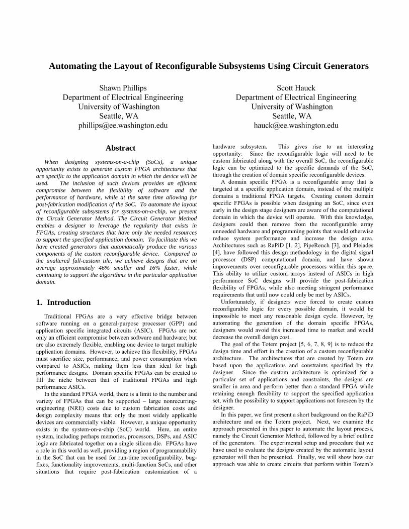
Figure 1: Block diagram of one full-custom RaPiD II cell. Up to thirty of these cells are placed along the horizontal axis. Data flows through the array along the horizontal axis in both left-to-right and right-to-left directions, with vertical routing providing connections between functional units. The black boxes in the interconnect represent bus connectors, which can be used to connect tracks into long lines or to separate them into short lines.
In this manner, we have created a modified version of the RaPiD I tile. The RaPiD II tile, shown in Figure 1, was created to support as many application domains as were available to us. Various application domains were run on the RaPiD I architecture, with some of the domains failing. Resources were then slowly added to the RaPiD I tile until most of the domains could be placed and routed.
By using a large number of domains to create the RaPiD II tile, it was hoped that the final template would be able to support similar, but unknown domains in the future. This method of producing a tile that is capable of handling a wide range of application domains is not unique to this work. Designers of
fixed reconfigurable hardware must go through this same process when finalizing a tile design.
3. Totem
Traditional FPGAs are very good at random logic, and have been an efficient architecture in designs where the required performance lies somewhere between that of software running on a GPP and that of an ASIC. FPGAs have been able to achieve this by providing flexibility, regardless of whether a designer is able to leverage all of it. Unfortunately, the overhead associated with this flexibility costs the FPGA in power, performance, and area when compared to an ASIC.
Architecture Generator
Architecture Description
*
+ LUT
VLSI Layout
Generator
P&R Tool Generator
Place
Route
Circuit
10010110...
ConstraintsDomain
Description
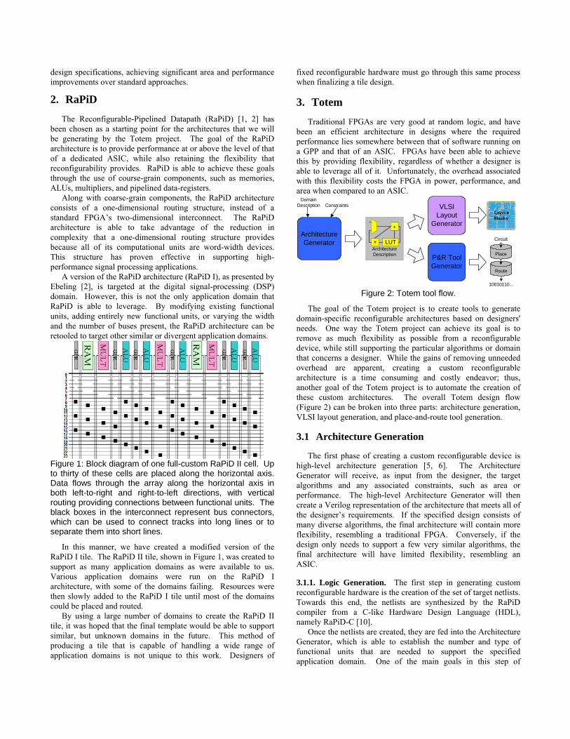
Figure 2: Totem tool flow.
The goal of the Totem project is to create tools to generate domain-specific reconfigurable architectures based on designers' needs. One way the Totem project can achieve its goal is to remove as much flexibility as possible from a reconfigurable device, while still supporting the particular algorithms or domain that concerns a designer. While the gains of removing unneeded overhead are apparent, creating a custom reconfigurable architecture is a time consuming and costly endeavor; thus, another goal of the Totem project is to automate the creation of these custom architectures. The overall Totem design flow (Figure 2) can be broken into three parts: architecture generation, VLSI layout generation, and place-and-route tool generation.
3.1 Architecture Generation
The first phase of creating a custom reconfigurable device is high-level architecture generation [5, 6]. The Architecture Generator will receive, as input from the designer, the target algorithms and any associated constraints, such as area or performance. The high-level Architecture Generator will then create a Verilog representation of the architecture that meets all of the designer’s requirements. If the specified design consists of many diverse algorithms, the final architecture will contain more flexibility, resembling a traditional FPGA. Conversely, if the design only needs to support a few very similar algorithms, the final architecture will have limited flexibility, resembling an ASIC.
3.1.1. Logic Generation. The first step in generating custom reconfigurable hardware is the creation of the set of target netlists. Towards this end, the netlists are synthesized by the RaPiD compiler from a C-like Hardware Design Language (HDL), namely RaPiD-C [10].
Once the netlists are created, they are fed into the Architecture Generator, which is able to establish the number and type of functional units that are needed to support the specified application domain. One of the main goals in this step of
architectural generation is the maximization of resource sharing, which in turn minimizes the number of functional units and routing resources needed to represent the application domain. Designers still have the option of adding more flexibility to devices by increasing the number and type of functional units instead of using the minimum number needed to support the application domain.
Currently all of the netlists in the application domain must be able to run in their entirety without any type of rescheduling. This is a big drawback with the current version of the Totem project, since it can lead to larger and slower architectures, however, this will be addressed in future versions. The absence of rescheduling implies that the minimum number of a particular type of functional unit needed in silicon is the maximum number needed by any netlist in the application domain. For example, if an application domain is represented by two netlists A and B, and netlist A needs 10 multipliers and 15 data-registers, and netlist B needs 5 multipliers and 30 data-registers, then the generated architecture will consist of 10 multipliers and 30 data-registers. Once the type and number of functional units is established, they then must be placed.
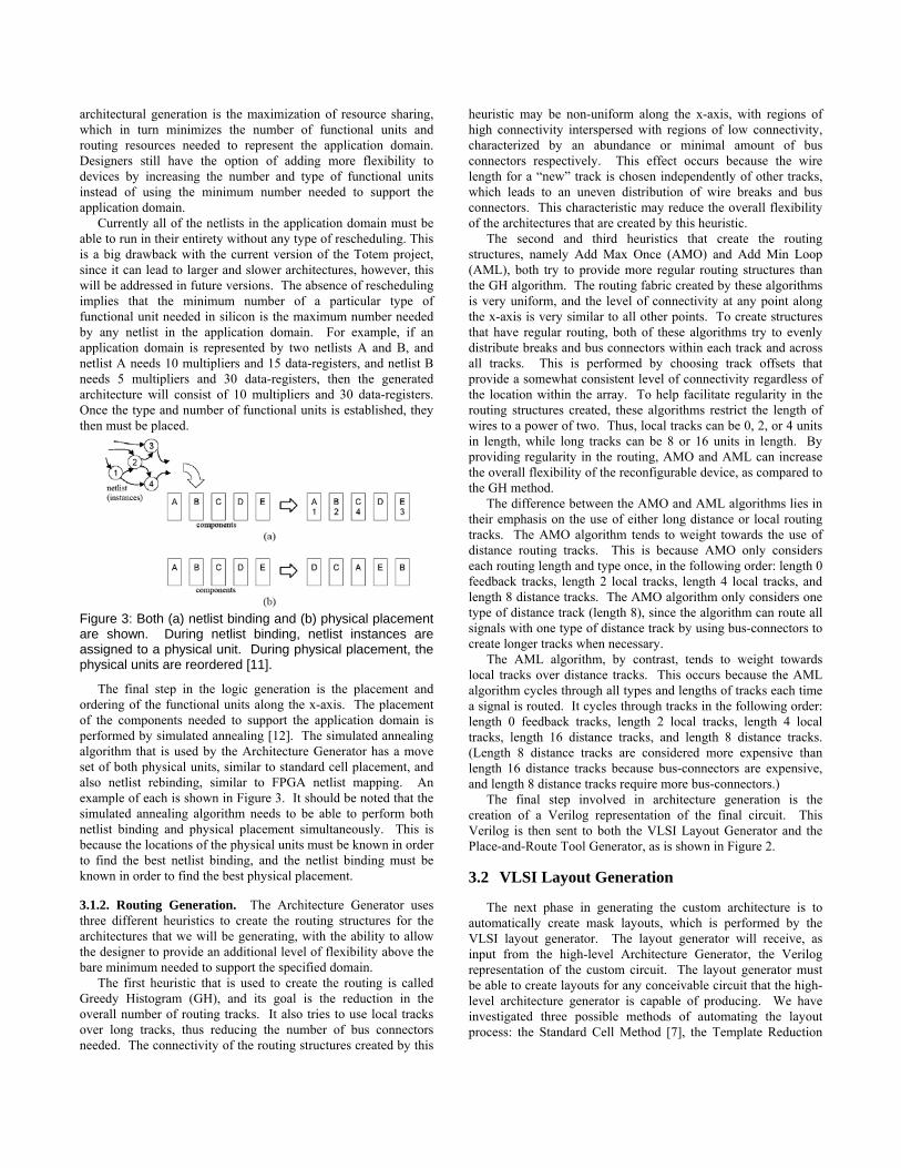
Figure 3: Both (a) netlist binding and (b) physical placement are shown. During netlist binding, netlist instances are assigned to a physical unit. During physical placement, the physical units are reordered [11].
The final step in the logic generation is the placement and ordering of the functional units along the x-axis. The placement of the components needed to support the application domain is performed by simulated annealing [12]. The simulated annealing algorithm that is used by the Architecture Generator has a move set of both physical units, similar to standard cell placement, and also netlist rebinding, similar to FPGA netlist mapping. An example of each is shown in Figure 3. It should be noted that the simulated annealing algorithm needs to be able to perform both netlist binding and physical placement simultaneously. This is because the locations of the physical units must be known in order to find the best netlist binding, and the netlist binding must be known in order to find the best physical placement.
3.1.2. Routing Generation. The Architecture Generator uses three different heuristics to create the routing structures for the architectures that we will be generating, with the ability to allow the designer to provide an additional level of flexibility above the bare minimum needed to support the specified domain.
The first heuristic that is used to create the routing is called Greedy Histogram (GH), and its goal is the reduction in the overall number of routing tracks. It also tries to use local tracks over long tracks, thus reducing the number of bus connectors needed. The connectivity of the routing structures created by this
heuristic may be non-uniform along the x-axis, with regions of high connectivity interspersed with regions of low connectivity, characterized by an abundance or minimal amount of bus connectors respectively. This effect occurs because the wire length for a “new” track is chosen independently of other tracks, which leads to an uneven distribution of wire breaks and bus connectors. This characteristic may reduce the overall flexibility of the architectures that are created by this heuristic.
The second and third heuristics that create the routing structures, namely Add Max Once (AMO) and Add Min Loop (AML), both try to provide more regular routing structures than the GH algorithm. The routing fabric created by these algorithms is very uniform, and the level of connectivity at any point along the x-axis is very similar to all other points. To create structures that have regular routing, both of these algorithms try to evenly distribute breaks and bus connectors within each track and across all tracks. This is performed by choosing track offsets that provide a somewhat consistent level of connectivity regardless of the location within the array. To help facilitate regularity in the routing structures created, these algorithms restrict the length of wires to a power of two. Thus, local tracks can be 0, 2, or 4 units in length, while long tracks can be 8 or 16 units in length. By providing regularity in the routing, AMO and AML can increase the overall flexibility of the reconfigurable device, as compared to the GH method.
The difference between the AMO and AML algorithms lies in their emphasis on the use of either long distance or local routing tracks. The AMO algorithm tends to weight towards the use of distance routing tracks. This is because AMO only considers each routing length and type once, in the following order: length 0 feedback tracks, length 2 local tracks, length 4 local tracks, and length 8 distance tracks. The AMO algorithm only considers one type of distance track (length 8), since the algorithm can route all signals with one type of distance track by using bus-connectors to create longer tracks when necessary.
The AML algorithm, by contrast, tends to weight towards local tracks over distance tracks. This occurs because the AML algorithm cycles through all types and lengths of tracks each time a signal is routed. It cycles through tracks in the following order: length 0 feedback tracks, length 2 local tracks, length 4 local tracks, length 16 distance tracks, and length 8 distance tracks. (Length 8 distance tracks are considered more expensive than length 16 distance tracks because bus-connectors are expensive, and length 8 distance tracks require more bus-connectors.)
The final step involved in architecture generation is the creation of a Verilog representation of the final circuit. This Verilog is then sent to both the VLSI Layout Generator and the Place-and-Route Tool Generator, as is shown in Figure 2.
3.2 VLSI Layout Generation
The next phase in generating the custom architecture is to automatically create mask layouts, which is performed by the VLSI layout generator. The layout generator will receive, as input from the high-level Architecture Generator, the Verilog representation of the custom circuit. The layout generator must be able to create layouts for any conceivable circuit that the high-level architecture generator is capable of producing. We have investigated three possible methods of automating the layout process: the Standard Cell Method [7], the Template Reduction
Method [9], and, the Circuit Generator Method (the focus of this paper).
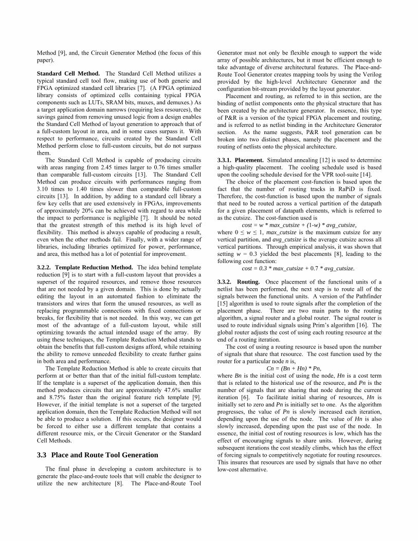
Standard Cell Method. The Standard Cell Method utilizes a typical standard cell tool flow, making use of both generic and FPGA optimized standard cell libraries [7]. (A FPGA optimized library consists of optimized cells containing typical FPGA components such as LUTs, SRAM bits, muxes, and demuxes.) As a target application domain narrows (requiring less resources), the savings gained from removing unused logic from a design enables the Standard Cell Method of layout generation to approach that of a full-custom layout in area, and in some cases surpass it. With respect to performance, circuits created by the Standard Cell Method perform close to full-custom circuits, but do not surpass them.
The Standard Cell Method is capable of producing circuits with areas ranging from 2.45 times larger to 0.76 times smaller than comparable full-custom circuits [13]. The Standard Cell Method can produce circuits with performances ranging from 3.10 times to 1.40 times slower than comparable full-custom circuits [13]. In addition, by adding to a standard cell library a few key cells that are used extensively in FPGAs, improvements of approximately 20% can be achieved with regard to area while the impact to performance is negligible [7]. It should be noted that the greatest strength of this method is its high level of flexibility. This method is always capable of producing a result, even when the other methods fail. Finally, with a wider range of libraries, including libraries optimized for power, performance, and area, this method has a lot of potential for improvement.
3.2.2. Template Reduction Method. The idea behind template reduction [9] is to start with a full-custom layout that provides a superset of the required resources, and remove those resources that are not needed by a given domain. This is done by actually editing the layout in an automated fashion to eliminate the transistors and wires that form the unused resources, as well as replacing programmable connections with fixed connections or breaks, for flexibility that is not needed. In this way, we can get most of the advantage of a full-custom layout, while still optimizing towards the actual intended usage of the array. By using these techniques, the Template Reduction Method stands to obtain the benefits that full-custom designs afford, while retaining the ability to remove unneeded flexibility to create further gains in both area and performance.
The Template Reduction Method is able to create circuits that perform at or better than that of the initial full-custom template. If the template is a superset of the application domain, then this method produces circuits that are approximately 47.6% smaller and 8.75% faster than the original feature rich template [9]. However, if the initial template is not a superset of the targeted application domain, then the Template Reduction Method will not be able to produce a solution. If this occurs, the designer would be forced to either use a different template that contains a different resource mix, or the Circuit Generator or the Standard Cell Methods.
3.3 Place and Route Tool Generation
The final phase in developing a custom architecture is to generate the place-and-route tools that will enable the designer to utilize the new architecture [8]. The Place-and-Route Tool
Generator must not only be flexible enough to support the wide array of possible architectures, but it must be efficient enough to take advantage of diverse architectural features. The Place-and-Route Tool Generator creates mapping tools by using the Verilog provided by the high-level Architecture Generator and the configuration bit-stream provided by the layout generator.
Placement and routing, as referred to in this section, are the binding of netlist components onto the physical structure that has been created by the architecture generator. In essence, this type of P&R is a version of the typical FPGA placement and routing, and is referred to as netlist binding in the Architecture Generator section. As the name suggests, P&R tool generation can be broken into two distinct phases, namely the placement and the routing of netlists onto the physical architecture.
3.3.1. Placement. Simulated annealing [12] is used to determine a high-quality placement. The cooling schedule used is based upon the cooling schedule devised for the VPR tool-suite [14].
The choice of the placement cost-function is based upon the fact that the number of routing tracks in RaPiD is fixed. Therefore, the cost-function is based upon the number of signals that need to be routed across a vertical partition of the datapath for a given placement of datapath elements, which is referred to as the cutsize. The cost-function used is
cost = w * max_cutsize + (1-w) * avg_cutsize, where 0 ≤ w ≤ 1, max_cutsize is the maximum cutsize for any vertical partition, and avg_cutsize is the average cutsize across all vertical partitions. Through empirical analysis, it was shown that setting w = 0.3 yielded the best placements [8], leading to the following cost function:
cost = 0.3 * max_cutsize + 0.7 * avg_cutsize.
3.3.2. Routing. Once placement of the functional units of a netlist has been performed, the next step is to route all of the signals between the functional units. A version of the Pathfinder [15] algorithm is used to route signals after the completion of the placement phase. There are two main parts to the routing algorithm, a signal router and a global router. The signal router is used to route individual signals using Prim’s algorithm [16]. The global router adjusts the cost of using each routing resource at the end of a routing iteration.
The cost of using a routing resource is based upon the number of signals that share that resource. The cost function used by the router for a particular node n is,
Cn = (Bn + Hn) * Pn, where Bn is the initial cost of using the node, Hn is a cost term that is related to the historical use of the resource, and Pn is the number of signals that are sharing that node during the current iteration [6]. To facilitate initial sharing of resources, Hn is initially set to zero and Pn is initially set to one. As the algorithm progresses, the value of Pn is slowly increased each iteration, depending upon the use of the node. The value of Hn is also slowly increased, depending upon the past use of the node. In essence, the initial cost of routing resources is low, which has the effect of encouraging signals to share units. However, during subsequent iterations the cost steadily climbs, which has the effect of forcing signals to competitively negotiate for routing resources. This insures that resources are used by signals that have no other low-cost alternative.
4. Approach
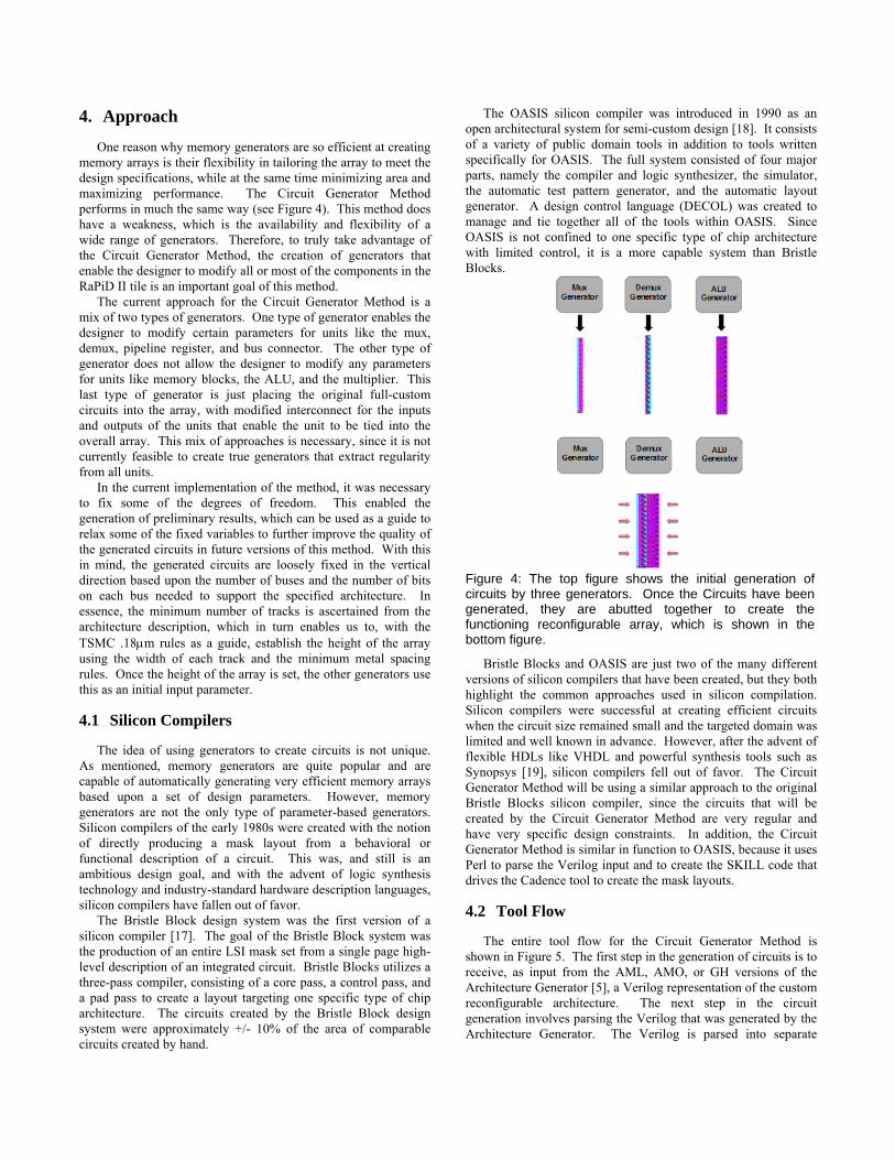
One reason why memory generators are so efficient at creating memory arrays is their flexibility in tailoring the array to meet the design specifications, while at the same time minimizing area and maximizing performance. The Circuit Generator Method performs in much the same way (see Figure 4). This method does have a weakness, which is the availability and flexibility of a wide range of generators. Therefore, to truly take advantage of the Circuit Generator Method, the creation of generators that enable the designer to modify all or most of the components in the RaPiD II tile is an important goal of this method.
The current approach for the Circuit Generator Method is a mix of two types of generators. One type of generator enables the designer to modify certain parameters for units like the mux, demux, pipeline register, and bus connector. The other type of generator does not allow the designer to modify any parameters for units like memory blocks, the ALU, and the multiplier. This last type of generator is just placing the original full-custom circuits into the array, with modified interconnect for the inputs and outputs of the units that enable the unit to be tied into the overall array. This mix of approaches is necessary, since it is not currently feasible to create true generators that extract regularity from all units.
In the current implementation of the method, it was necessary to fix some of the degrees of freedom. This enabled the generation of preliminary results, which can be used as a guide to relax some of the fixed variables to further improve the quality of the generated circuits in future versions of this method. With this in mind, the generated circuits are loosely fixed in the vertical direction based upon the number of buses and the number of bits on each bus needed to support the specified architecture. In essence, the minimum number of tracks is ascertained from the architecture description, which in turn enables us to, with the TSMC .18µm rules as a guide, establish the height of the array using the width of each track and the minimum metal spacing rules. Once the height of the array is set, the other generators use this as an initial input parameter.
4.1 Silicon Compilers
The idea of using generators to create circuits is not unique. As mentioned, memory generators are quite popular and are capable of automatically generating very efficient memory arrays based upon a set of design parameters. However, memory generators are not the only type of parameter-based generators. Silicon compilers of the early 1980s were created with the notion of directly producing a mask layout from a behavioral or functional description of a circuit. This was, and still is an ambitious design goal, and with the advent of logic synthesis technology and industry-standard hardware description languages, silicon compilers have fallen out of favor.
The Bristle Block design system was the first version of a silicon compiler [17]. The goal of the Bristle Block system was the production of an entire LSI mask set from a single page high-level description of an integrated circuit. Bristle Blocks utilizes a three-pass compiler, consisting of a core pass, a control pass, and a pad pass to create a layout targeting one specific type of chip architecture. The circuits created by the Bristle Block design system were approximately +/- 10% of the area of comparable circuits created by hand.
The OASIS silicon compiler was introduced in 1990 as an open architectural system for semi-custom design [18]. It consists of a variety of public domain tools in addition to tools written specifically for OASIS. The full system consisted of four major parts, namely the compiler and logic synthesizer, the simulator, the automatic test pattern generator, and the automatic layout generator. A design control language (DECOL) was created to manage and tie together all of the tools within OASIS. Since OASIS is not confined to one specific type of chip architecture with limited control, it is a more capable system than Bristle Blocks.
Figure 4: The top figure shows the initial generation of circuits by three generators. Once the Circuits have been generated, they are abutted together to create the functioning reconfigurable array, which is shown in the bottom figure.
Bristle Blocks and OASIS are just two of the many different versions of silicon compilers that have been created, but they both highlight the common approaches used in silicon compilation. Silicon compilers were successful at creating efficient circuits when the circuit size remained small and the targeted domain was limited and well known in advance. However, after the advent of flexible HDLs like VHDL and powerful synthesis tools such as Synopsys [19], silicon compilers fell out of favor. The Circuit Generator Method will be using a similar approach to the original Bristle Blocks silicon compiler, since the circuits that will be created by the Circuit Generator Method are very regular and have very specific design constraints. In addition, the Circuit Generator Method is similar in function to OASIS, because it uses Perl to parse the Verilog input and to create the SKILL code that drives the Cadence tool to create the mask layouts.
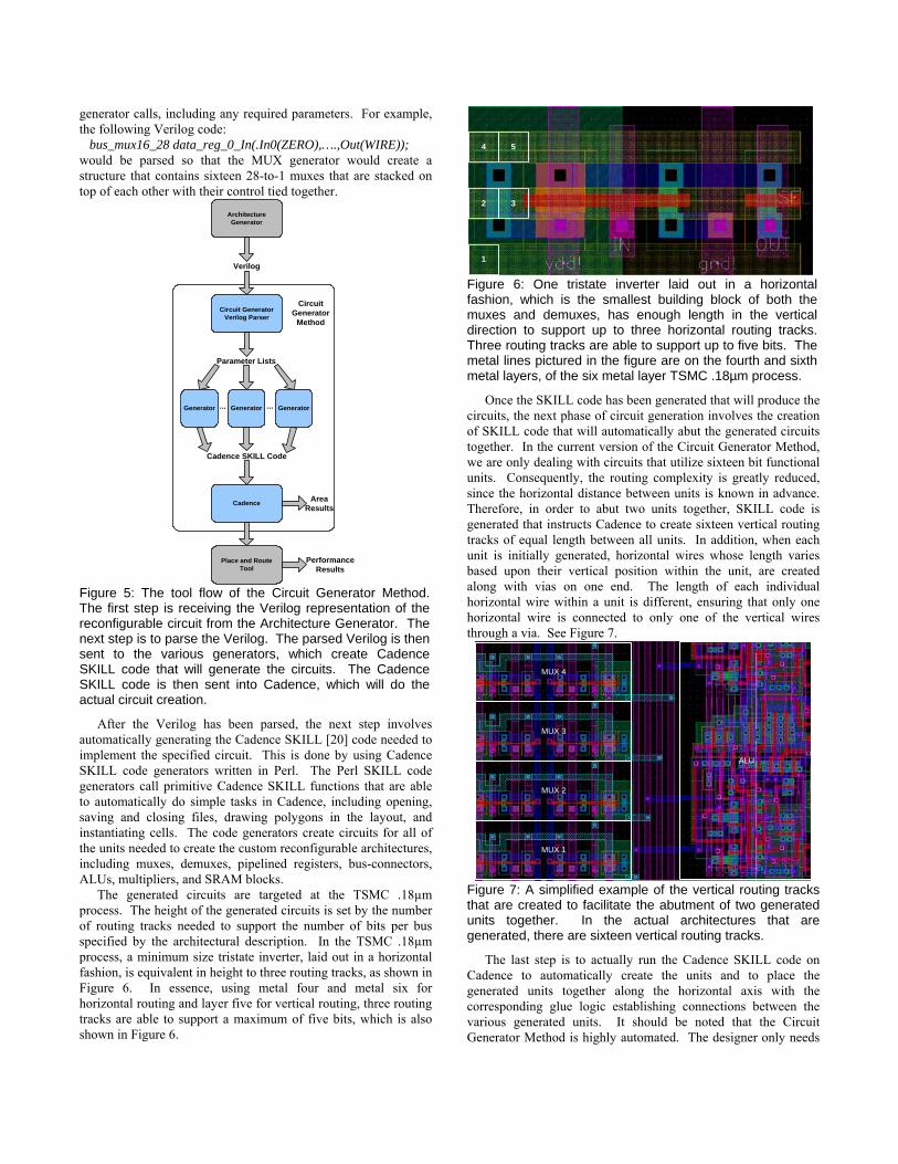
4.2 Tool Flow
The entire tool flow for the Circuit Generator Method is shown in Figure 5. The first step in the generation of circuits is to receive, as input from the AML, AMO, or GH versions of the Architecture Generator [5], a Verilog representation of the custom reconfigurable architecture. The next step in the circuit generation involves parsing the Verilog that was generated by the Architecture Generator. The Verilog is parsed into separate
generator calls, including any required parameters. For example, the following Verilog code: bus_mux16_28 data_reg_0_In(.In0(ZERO),….,Out(WIRE)); would be parsed so that the MUX generator would create a structure that contains sixteen 28-to-1 muxes that are stacked on top of each other with their control tied together.
Architecture Generator
Verilog
Circuit Generator Verilog Parser
Parameter Lists
Cadence SKILL Code
Generator Generator Generator......
Cadence
Circuit Generator
Method
Area Results
Place and Route Tool
Performance Results
Figure 5: The tool flow of the Circuit Generator Method. The first step is receiving the Verilog representation of the reconfigurable circuit from the Architecture Generator. The next step is to parse the Verilog. The parsed Verilog is then sent to the various generators, which create Cadence SKILL code that will generate the circuits. The Cadence SKILL code is then sent into Cadence, which will do the actual circuit creation.
After the Verilog has been parsed, the next step involves automatically generating the Cadence SKILL [20] code needed to implement the specified circuit. This is done by using Cadence SKILL code generators written in Perl. The Perl SKILL code generators call primitive Cadence SKILL functions that are able to automatically do simple tasks in Cadence, including opening, saving and closing files, drawing polygons in the layout, and instantiating cells. The code generators create circuits for all of the units needed to create the custom reconfigurable architectures, including muxes, demuxes, pipelined registers, bus-connectors, ALUs, multipliers, and SRAM blocks.
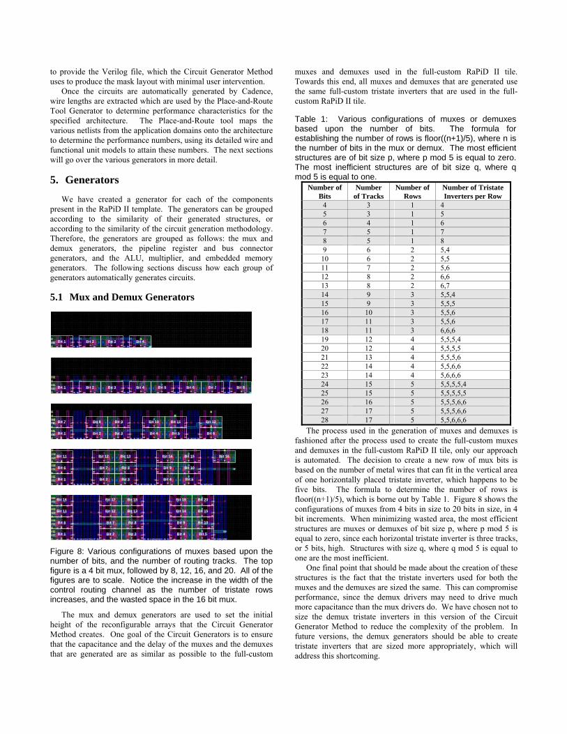
The generated circuits are targeted at the TSMC .18µm process. The height of the generated circuits is set by the number of routing tracks needed to support the number of bits per bus specified by the architectural description. In the TSMC .18µm process, a minimum size tristate inverter, laid out in a horizontal fashion, is equivalent in height to three routing tracks, as shown in Figure 6. In essence, using metal four and metal six for horizontal routing and layer five for vertical routing, three routing tracks are able to support a maximum of five bits, which is also shown in Figure 6.
1
2 3
4 5
Figure 6: One tristate inverter laid out in a horizontal fashion, which is the smallest building block of both the muxes and demuxes, has enough length in the vertical direction to support up to three horizontal routing tracks. Three routing tracks are able to support up to five bits. The metal lines pictured in the figure are on the fourth and sixth metal layers, of the six metal layer TSMC .18µm process.
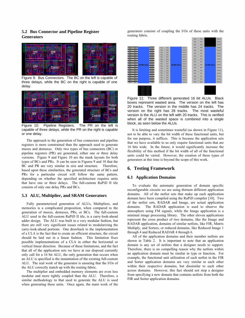
Once the SKILL code has been generated that will produce the circuits, the next phase of circuit generation involves the creation of SKILL code that will automatically abut the generated circuits together. In the current version of the Circuit Generator Method, we are only dealing with circuits that utilize sixteen bit functional units. Consequently, the routing complexity is greatly reduced, since the horizontal distance between units is known in advance. Therefore, in order to abut two units together, SKILL code is generated that instructs Cadence to create sixteen vertical routing tracks of equal length between all units. In addition, when each unit is initially generated, horizontal wires whose length varies based upon their vertical position within the unit, are created along with vias on one end. The length of each individual horizontal wire within a unit is different, ensuring that only one horizontal wire is connected to only one of the vertical wires through a via. See Figure 7.
MUX 1
MUX 2
MUX 3
MUX 4
ALU
Figure 7: A simplified example of the vertical routing tracks that are created to facilitate the abutment of two generated units together. In the actual architectures that are generated, there are sixteen vertical routing tracks.
The last step is to actually run the Cadence SKILL code on Cadence to automatically create the units and to place the generated units together along the horizontal axis with the corresponding glue logic establishing connections between the various generated units. It should be noted that the Circuit Generator Method is highly automated. The designer only needs
to provide the Verilog file, which the Circuit Generator Method uses to produce the mask layout with minimal user intervention.
Once the circuits are automatically generated by Cadence, wire lengths are extracted which are used by the Place-and-Route Tool Generator to determine performance characteristics for the specified architecture. The Place-and-Route tool maps the various netlists from the application domains onto the architecture to determine the performance numbers, using its detailed wire and functional unit models to attain these numbers. The next sections will go over the various generators in more detail.
5. Generators
We have created a generator for each of the components present in the RaPiD II template. The generators can be grouped according to the similarity of their generated structures, or according to the similarity of the circuit generation methodology. Therefore, the generators are grouped as follows: the mux and demux generators, the pipeline register and bus connector generators, and the ALU, multiplier, and embedded memory generators. The following sections discuss how each group of generators automatically generates circuits.
5.1 Mux and Demux Generators
Bit 1 Bit 2 Bit 3 Bit 4
Bit 1 Bit 2 Bit 3 Bit 4 Bit 5 Bit 6 Bit 7 Bit 8
Bit 1 Bit 2 Bit 3 Bit 4 Bit 5 Bit 6
Bit 7 Bit 8 Bit 9 Bit 10 Bit 11 Bit 12
Bit 1 Bit 2 Bit 3 Bit 4 Bit 5
Bit 6 Bit 7 Bit 8 Bit 9 Bit 10
Bit 16Bit 11 Bit 12 Bit 13 Bit 14 Bit 15
Bit 1
Bit 6
Bit 11
Bit 16
Bit 2
Bit 7
Bit 12
Bit 17
Bit 3
Bit 8
Bit 13
Bit 18
Bit 4
Bit 9
Bit 14
Bit 19
Bit 5
Bit 10
Bit 15
Bit 20
Figure 8: Various configurations of muxes based upon the number of bits, and the number of routing tracks. The top figure is a 4 bit mux, followed by 8, 12, 16, and 20. All of the figures are to scale. Notice the increase in the width of the control routing channel as the number of tristate rows increases, and the wasted space in the 16 bit mux.
The mux and demux generators are used to set the initial height of the reconfigurable arrays that the Circuit Generator Method creates. One goal of the Circuit Generators is to ensure that the capacitance and the delay of the muxes and the demuxes that are generated are as similar as possible to the full-custom
muxes and demuxes used in the full-custom RaPiD II tile. Towards this end, all muxes and demuxes that are generated use the same full-custom tristate inverters that are used in the full-custom RaPiD II tile.
Table 1: Various configurations of muxes or demuxes based upon the number of bits. The formula for establishing the number of rows is floor((n+1)/5), where n is the number of bits in the mux or demux. The most efficient structures are of bit size p, where p mod 5 is equal to zero. The most inefficient structures are of bit size q, where q mod 5 is equal to one.
Number of Bits
Number of Tracks
Number of Rows
Number of Tristate Inverters per Row
4 3 1 4 5 3 1 5 6 4 1 6 7 5 1 7 8 5 1 8 9 6 2 5,4
10 6 2 5,5 11 7 2 5,6 12 8 2 6,6 13 8 2 6,7 14 9 3 5,5,4 15 9 3 5,5,5 16 10 3 5,5,6 17 11 3 5,5,6 18 11 3 6,6,6 19 12 4 5,5,5,4 20 12 4 5,5,5,5 21 13 4 5,5,5,6 22 14 4 5,5,6,6 23 14 4 5,6,6,6 24 15 5 5,5,5,5,4 25 15 5 5,5,5,5,5 26 16 5 5,5,5,6,6 27 17 5 5,5,5,6,6 28 17 5 5,5,6,6,6
The process used in the generation of muxes and demuxes is fashioned after the process used to create the full-custom muxes and demuxes in the full-custom RaPiD II tile, only our approach is automated. The decision to create a new row of mux bits is based on the number of metal wires that can fit in the vertical area of one horizontally placed tristate inverter, which happens to be five bits. The formula to determine the number of rows is floor((n+1)/5), which is borne out by Table 1. Figure 8 shows the configurations of muxes from 4 bits in size to 20 bits in size, in 4 bit increments. When minimizing wasted area, the most efficient structures are muxes or demuxes of bit size p, where p mod 5 is equal to zero, since each horizontal tristate inverter is three tracks, or 5 bits, high. Structures with size q, where q mod 5 is equal to one are the most inefficient.
One final point that should be made about the creation of these structures is the fact that the tristate inverters used for both the muxes and the demuxes are sized the same. This can compromise performance, since the demux drivers may need to drive much more capacitance than the mux drivers do. We have chosen not to size the demux tristate inverters in this version of the Circuit Generator Method to reduce the complexity of the problem. In future versions, the demux generators should be able to create tristate inverters that are sized more appropriately, which will address this shortcoming.
5.2 Bus Connector and Pipeline Register Generators
Figure 9: Bus Connectors. The BC on the left is capable of three delays, while the BC on the right is capable of one delay.
Figure 10: Pipeline Registers. The PR on the left is capable of three delays, while the PR on the right is capable or one delay.
The approach to the generation of bus connectors and pipeline registers is more constrained than the approach used to generate muxes and demuxes. Only two types of bus connectors (BC) or pipeline registers (PR) are generated, either one or three delay versions. Figure 9 and Figure 10 are the mask layouts for both types of BCs and PRs. It can be seen in Figures 9 and 10 that the BC and PR are very similar in size and structure. Therefore, based upon these similarities, the generated structure of BCs and PRs for a particular circuit will follow the same pattern, depending on whether the specified architecture requires units that have one or three delays. The full-custom RaPiD II tile consists of only one delay PRs and BCs.
5.3 ALU, Multiplier, and SRAM Generators
Fully parameterized generation of ALUs, Multipliers, and memories is a complicated proposition, when compared to the generation of muxes, demuxes, PRs, or BCs. The full-custom ALU used in the full-custom RaPiD II tile, is a carry-look-ahead adder design. The ALU was built in a very modular fashion, but there are still very significant issues related to modularizing the carry-look-ahead portions. One drawback to the implementation of a CLA is the fact that to create an efficient structure, the circuit should be laid out in a linear fashion. This limitation fixes possible implementations of a CLA in either the horizontal or vertical linear direction. Because of these limitations, and the fact that all of the application sets we have at our disposal currently only call for a 16 bit ALU, the only generation that occurs when an ALU is specified is the instantiation of the existing full-custom ALU. The real work of the generator is ensuring that the I/Os of the ALU correctly match up with the routing fabric.
The multiplier and embedded memory elements are even less modular and more tightly coupled than the ALU. Therefore, a similar methodology to that used to generate the ALU is used when generating these units. Once again, the main work of the
generators consists of coupling the I/Os of these units with the routing fabric.
16 Bit ALU
Mux Demux
Mux
Mux
Mux
Mux
Mux
Mux
Mux
Mux
Mux
Mux
Mux
Mux
Mux
Mux
Mux
Mux
Mux
Mux
Mux
Mux
Mux
Mux
Mux
Mux
Mux
Mux
Mux
Mux
Mux
Mux
Mux
Demux
Demux
Demux
Demux
Demux
Demux
Demux
Demux
Demux
Demux
Demux
Demux
Demux
Demux
Demux
16 Bit ALU
Mux
Mux
Mux
Mux
Mux
Mux
Mux
Mux
Mux
Mux
Mux
Mux
Mux
Mux
Mux
Mux
Mux
Mux
Mux
Mux
Mux
Mux
Mux
Mux
Mux
Mux
Mux
Mux
Mux
Mux
Mux
Mux Demux
Demux
Demux
Demux
Demux
Demux
Demux
Demux
Demux
Demux
Demux
Demux
Demux
Demux
Demux
Demux
16 Bit ALU
Mux
Mux
Mux
Mux
Mux
Mux
Mux
Mux
Mux
Mux
Mux
Mux
Mux
Mux
Mux
Mux
Mux
Mux
Mux
Mux
Mux
Mux
Mux
Mux
Mux
Mux
Mux
Mux
Mux
Mux
Mux
Mux
Demux
Demux
Demux
Demux
Demux
Demux
Demux
Demux
Demux
Demux
Demux
Demux
Demux
Demux
Demux
Demux
Figure 11: Three different generated 16 bit ALUs. Black boxes represent wasted area. The version on the left has 20 tracks. The version in the middle has 24 tracks. The version on the right has 28 tracks. The most wasteful version is the ALU on the left with 20 tracks. This is verified when all of the wasted space is combined into a single block, as seen below the ALUs.
It is limiting and sometimes wasteful (as shown in Figure 11), not to be able to vary the bit width of these functional units, but for our purpose, it suffices. This is because the application sets that we have available to us only require functional units that are 16 bits wide. In the future, it would significantly increase the flexibility of this method if the bit width of all of the functional units could be varied. However, the creation of these types of generators at this time is beyond the scope of this work.
6. Testing Framework
6.1 Application Domains
To evaluate the automatic generation of domain specific reconfigurable circuits we are using thirteen different application domains. All of the netlist sets that make up each application domain have been compiled using the RaPiD compiler [10]. Two of the netlist sets, RADAR and Image, are actual application domains. The RADAR application is used to observe the atmosphere using FM signals, while the Image application is a minimal image processing library. The other eleven applications represent the cross product of two domains, like the Image and RADAR application, domains of similar netlists, like FIR, Matrix Multiply, and Sorters, or reduced domains, like Reduced Image 1 through 4 and Reduced RADAR 4 through 6.
All of the application domains and their member netlists are shown in Table 2. It is important to note that an application domain is any set of netlists that a designer needs to support. Therefore, there is no compelling reason why the netlists within an application domain must be similar in type or function. For example, the functional unit utilization of each netlist in the FIR and Sorter application domains are very similar to each other within their respective domains, but dissimilar to each other across domains. However, this fact should not stop a designer from specifying a new domain that contains netlists from both the FIR and Sorter application domains.
6.2 Percent Utilization
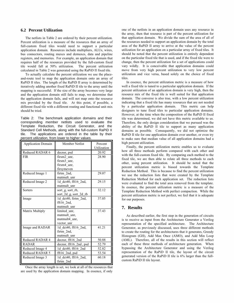
The netlists in Table 2 are ordered by their percent utilization. Percent utilization is a measure of the resources that an array of full-custom fixed tiles would need to support a particular application domain. Resources include multipliers, ALUs, wires, bus connectors, routing muxes and demuxes, data and pipeline registers, and memories. For example, an application domain that requires half of the resources provided by the full-custom fixed tile would fall at 50% utilization. The percent utilization calculated in Table 2 was generated using the RaPiD II fixed tile.
To actually calculate the percent utilization we use the place-and-route tool to map the application domain onto an array of RaPiD II tiles. The length of the RaPiD II array is determined by iteratively adding another fixed RaPiD II tile to the array until the mapping is successful. If the size of the array becomes very large and the application domain still fails to map, we determine that the application domain fails, and will not map onto the resource mix provided by the fixed tile. At this point, if possible, a different fixed tile with a different routing and functional unit mix should be tried.
Table 2: The benchmark application domains and their corresponding member netlists used to evaluate the Template Reduction, the Circuit Generator, and the Standard Cell Methods, along with the full-custom RaPiD II tile. The applications are ordered in the table by their percent utilization, from lower to higher values.
Application Domain Member Netlist Percent Utilization
Reduced RADAR 6 decnsr, psd 20.92 FIR firsm2_unr,
firsm3_unr, firsm4_unr, firsymeven
28.90
Reduced Image 1 firtm_2nd, matmult_unr
29.07
Reduced Image 2 1d_dct40, fft16_2nd, matmult_unr
29.15
Sorters sort_g, sort_rb, sort_2d_g, sort_2d_rb
32.12
Image 1d_dct40, firtm_2nd, fft16_2nd, matmult_unr
37.05
Matrix Multiply limited_unr, matmult_unr, matmult4_unr, vector_unr
37.43
Image and RADAR 1d_dct40, fft16_2nd, firtm_2nd, matmult_unr
41.21
Reduced RADAR 4 decnsr, fft16_2nd 50.88 RADAR decnsr, fft16_2nd , psd 52.79 Reduced Image 4 1d_dct40, fft16_2nd 52.82 Reduced RADAR 5 fft16_2nd, psd 53.54 Reduced Image 3 1d_dct40, fft16_2nd,
firtm_2nd 60.18
Once the array length is set, we look at all of the resources that are used by the application domain mapping. In essence, if only
one of the netlists in an application domain uses any resource in the array, then that resource is part of the percent utilization for that application domain. We divide the sum of the area of all of the resources needed to support an application domain by the total area of the RaPiD II array to arrive at the value of the percent utilization for an application on a particular array of fixed tiles. It should be noted that the percent utilization is entirely dependent on the particular fixed tile that is used, and if the fixed tile were to change, then the percent utilization for a set of applications could vary wildly. It is conceivable that application domains could move from very high percent utilization to very low percent utilization and vice versa, based solely on the choice of fixed tiles.
In essence, the percent utilization metric is a measure of how well a fixed tile is tuned to a particular application domain. If the percent utilization of an application domain is very high, then the resource mix of the fixed tile is well suited for that application domain. The converse is also true, with a low percent utilization indicating that a fixed tile has many resources that are not needed by a particular application domain. This metric can help designers to tune fixed tiles to particular application domains. However, at the time when the composition of the RaPiD II fixed tile was determined, we did not have this metric available to us. Therefore, the only design consideration that we pursued was the ability of the RaPiD II tile to support as many application domains as possible. Consequently, we did not optimize the RaPiD II tile for one application domain over another, or even try to make sure that median value of all application domains had a high percent utilization.
Finally, the percent utilization metric enables us to evaluate how all three methods perform compared with each other and with the full-custom fixed tile. By comparing each method to the fixed tile, we are then able to relate all three methods to each other, using percent utilization. It should be noted that the percent utilization metric is biased towards the Template Reduction Method. This is because to find the percent utilization we use the reduction lists that were created by the Template Reduction Method for each application set. The reduction lists were evaluated to find the total area removed from the template. In essence, the percent utilization metric is a measure of the Template Reduction Method with perfect compaction. While the percent utilization metric is not perfect, we feel that it is adequate for our purposes.
7. Results
As described earlier, the first step in the generation of circuits is to receive as input from the Architecture Generator a Verilog representation of the specified architecture. The Architecture Generator, as previously discussed, uses three different methods to create the routing for the architectures that it generates, Greedy Histogram (GH), Add Max Once (AMO), and Add Min Loop (AML). Therefore, all of the results in this section will reflect each of these three methods of architecture generation. When bypassing the Architecture Generator and using the Verilog representation of the RaPiD II tile, the layout of the circuit generated version of the RaPiD II tile is 6% larger than the full-custom RaPiD II tile layout.
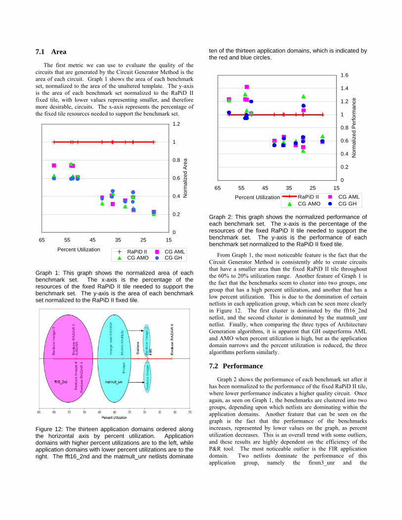
7.1 Area
The first metric we can use to evaluate the quality of the circuits that are generated by the Circuit Generator Method is the area of each circuit. Graph 1 shows the area of each benchmark set, normalized to the area of the unaltered template. The y-axis is the area of each benchmark set normalized to the RaPiD II fixed tile, with lower values representing smaller, and therefore more desirable, circuits. The x-axis represents the percentage of the fixed tile resources needed to support the benchmark set.
0
0.2
0.4
0.6
0.8
1
1.2
152535455565
Percent Utilization
Nor
mal
ized
Are
a
RaPiD II CG AMLCG AMO CG GH
Graph 1: This graph shows the normalized area of each benchmark set. The x-axis is the percentage of the resources of the fixed RaPiD II tile needed to support the benchmark set. The y-axis is the area of each benchmark set normalized to the RaPiD II fixed tile.
Figure 12: The thirteen application domains ordered along the horizontal axis by percent utilization. Application domains with higher percent utilizations are to the left, while application domains with lower percent utilizations are to the right. The fft16_2nd and the matmult_unr netlists dominate
ten of the thirteen application domains, which is indicated by the red and blue circles.
0
0.2
0.4
0.6
0.8
1
1.2
1.4
1.6
152535455565
Percent Utilization
Nor
mal
ized
Per
form
ance
RaPiD II CG AMLCG AMO CG GH
Graph 2: This graph shows the normalized performance of each benchmark set. The x-axis is the percentage of the resources of the fixed RaPiD II tile needed to support the benchmark set. The y-axis is the performance of each benchmark set normalized to the RaPiD II fixed tile.
From Graph 1, the most noticeable feature is the fact that the Circuit Generator Method is consistently able to create circuits that have a smaller area than the fixed RaPiD II tile throughout the 60% to 20% utilization range. Another feature of Graph 1 is the fact that the benchmarks seem to cluster into two groups, one group that has a high percent utilization, and another that has a low percent utilization. This is due to the domination of certain netlists in each application group, which can be seen more clearly in Figure 12. The first cluster is dominated by the fft16_2nd netlist, and the second cluster is dominated by the matmult_unr netlist. Finally, when comparing the three types of Architecture Generation algorithms, it is apparent that GH outperforms AML and AMO when percent utilization is high, but as the application domain narrows and the percent utilization is reduced, the three algorithms perform similarly.
7.2 Performance
Graph 2 shows the performance of each benchmark set after it has been normalized to the performance of the fixed RaPiD II tile, where lower performance indicates a higher quality circuit. Once again, as seen on Graph 1, the benchmarks are clustered into two groups, depending upon which netlists are dominating within the application domains. Another feature that can be seen on the graph is the fact that the performance of the benchmarks increases, represented by lower values on the graph, as percent utilization decreases. This is an overall trend with some outliers, and these results are highly dependent on the efficiency of the P&R tool. The most noticeable outlier is the FIR application domain. Two netlists dominate the performance of this application group, namely the firsm3_unr and the
firsymenven_unr, causing it to perform poorly. It should be noted that the P&R tool is unable to retime signals, as mentioned earlier. Therefore, any performance numbers generated by the P&R tool should only be used for relative comparisons of the three methods.
8. Conclusions
In this paper, we have presented the Circuit Generator Method for automating the layout of custom domain specific reconfigurable devices for SoC. This method is able to create circuits that perform better than that of the RaPiD II full-custom fixed tile, as long as the specified architecture does not require functional units or routing resources that do not have a corresponding generator. If this condition is met, then the Circuit Generator Method produces circuits that are approximately 46% smaller and 16% faster than the full-custom RaPiD II fixed tile.
The Circuit Generator Method performs very well when compared to the Standard Cell Method (which produces circuits with areas ranging from 2.45 times larger to 0.76 times smaller and performances ranging from 3.10 times to 1.40 times slower than the RaPiD II fixed tile [13]) and the Template Reduction Method (which produces circuits that are approximately 47.6% smaller and 8.75% faster than the RaPiD II fixed tile [9]). The Circuit Generator Method is able to leverage the regularity that exists in FPGAs when creating RaPiD-like structures. It can create structures that are more efficient than the Template Reduction Method, while not being bound to a particular template. In addition, the Circuit Generator Method is an additive method. Therefore, this method is less error prone than the Template Reduction Method since we are not cutting low-level components out of full-custom circuits.
However, the Circuit Generator Method has problems of its own. The creation of a wide range of generators can be as costly a proposition as creating a wide range of templates. Yet, to improve the Circuit Generator Method, providing a wide range of different types of generators is critical. To increase the quality of the circuits that the method creates, all of the generators should be able to handle a wide range of parameters. For example, in the current implementation of the Circuit Generator Method, the generators that create the functional units are unable to change the bit width of units that they create. However, it has been shown in previous work [7] that the largest impact on area is achieved through reducing the overall bit-width of the device that is created. Therefore, the creation of generators that are able to modify the bit width of the functional units could drastically increase the ability of the Circuit Generator Method to create higher quality circuits. Finally, if the Circuit Generator Method needs to create circuits that are targeted at low power, high performance, or small area, even more types of generators will be needed.
9. Future Work
The current version of the Circuit Generator Method is a first generation implementation. Therefore, there is potential for future improvement. One improvement that has the potential to drastically increase the flexibility of this method is the creation of fully parameterized generators for all of the functional units used in the RaPiD II tile. Another improvement would be the creation of additional generators for different types of functional units that
are currently not in the RaPiD II tile. By adding these additional generators, the Circuit Generator Method would be able to target a wider range of domains. Finally, the generators that have been created thus far are targeted at creating devices that have the smallest possible area. New generators that could target performance or power instead of just area would also provide designers with support for a wider range of application domains.
10. Acknowledgments
The authors would like to thank the RaPiD group, especially Carl Ebeling and Chris Fisher, for the RaPiD I layout used in this research. We also are indebted to Larry McMurchie for support on the Cadence tool-suite. This work was funded in part from grants from NSF and NASA. Shawn Phillips was supported in part by a MIT Lincoln Labs Research Fellowship. Scott Hauck was supported in part by an NSF CAREER award and an Alfred P. Sloan Research Fellowship.
11. References
[1] Darren C. Cronquist, Paul Franklin, Chris Fisher, Miguel Figueroa, and Carl Ebeling, “Architecture Design of Reconfigurable Pipelined Datapaths”, Twentieth Anniversary Conference on Advanced Research in VLSI, pp 23-40, 1999.
[2] C. Ebeling, D. C. Cronquist, P. Franklin, “RaPiD – Reconfigurable Pipelined Datapath”, 6th Annual Workshop on Field Programmable Logic and Applications, 1996.
[3] S. Goldstein, H. Schmit, M. Budiu, S. Cadambi, M. Moe, R. Taylor, “PipeRench: An Architecture and Compiler for Reconfigurable Computing”, IEEE Computer, 2000.
[4] A. Abnous and J. M. Rabaey, "Ultra-low-power domain-specific multimedia processors," Proc. of IEEE VLSI Signal Processing Workshop, Oct. 1996.
[5] K. Compton, S. Hauck, "Totem: Custom Reconfigurable Array Generation", IEEE Symposium on FPGAs for Custom Computing Machines Conference, 2001.
[6] K. Compton, A. Sharma, S. Phillips, S. Hauck, "Flexible Routing Architecture Generation for Domain-Specific Reconfigurable Subsystems", International Conference on Field Programmable Logic and Applications, pp. 59-68, 2002.
[7] S. Phillips, S. Hauck, "Automatic Layout of Domain-Specific Reconfigurable Subsystems for System-on-a-Chip", ACM/SIGDA Symposium on Field-Programmable Gate Arrays, pp. 165-173, 2002.
[8] A. Sharma, C. Ebeling, S. Hauck, "PipeRoute: A Pipelining-Aware Router for FPGAs", ACM/SIGDA Symposium on Field-Programmable Gate Arrays, pp. 68-77, 2003.
[9] S. Phillips, A. Sharma, S. Hauck, "Automating the Layout of Reconfigurable Subsytems Via Template Reduction", International Symposium on Field-Programmable Logic and Applications, pp. 857-861, 2004.
[10] D. C. Cronquist, P. Franklin, S.G. Berg, C. Ebeling, "Specifying and Compiling Applications for RaPiD", IEEE Symposium on FPGAs for Custom Computing Machines, 1998.
[11] Kathrine Compton, “Architecture Generation of Customized Reconfigurable Hardware”, Ph.D. Thesis, Northwestern University, Dept. of ECE, 2003.
[12] C. Sechen, VLSI Placement and Global Routing Using Simulated Annealing, Kluwer Academic Publishers, Boston, MA: 1988.
[13] Shawn Phillips, “Automating Layout of Reconfigurable Subsystems for Systems-on-a-Chip”, Ph.D. Thesis, University of Washington, Dept. of EE, 2004.
[14] V. Betz and J. Rose, “VPR: A New Packing, Placement and Routing Tool for FPGA Research,” Seventh International Workshop on Field-Programmable Logic and Applications, pp 213-222, 1997.
[15] Larry McMurchie and Carl Ebeling, “PathFinder: A Negotiation-Based Performance-Driven Router for FPGAs”, ACM Third International Symposium on Field-Programmable Gate Arrays, pp 111-117, 1995
[16] Thomas H.Cormen, Charles E. Leiserson, and Ronald L. Rivest, Introduction to Algorithms, The MIT Press, Cambridge, MA, Prim’s algorithm, pp 505-510, 1990.
[17] D. Johannsen, “Bristle Blocks: A silicon compiler”, Proc. 16th Design Automation Conf., 1979.
[18] G. Kedem, F. Brglez, K. Kozminski, “OASIS: A silicon compiler for semi-custom design”, Euro ASIC ’90, pp. 118-123, 1990.
[19] Synopsys, Inc., “Synopsys Online Documentation”, version 2000.05, 2000.
[20] Cadence Design Systems, Inc., “Openbook”, version 4.1, release IC 4.4.5, 1999.