atomic structure and energy of ∑ = 5 tilt boundaries in gold
TRANSCRIPT

Atomic Structure and Energy of Y_, = 5 Tilt Boundaries in Gold
FREDERIC COSANDEY, SIU-WAI CHAN, and PIERRE STADELMANN
The atomic structure of ~ = 5 (0 = 36.9 deg) [001] tilt boundaries in gold has been investigated by high-resolution electron microscopy (HREM). Image simulations and experimental condi- tions for observing grain boundary atomic structure in gold are presented. Two preferred ori- entations corresponding to symmetric {310} and asymmetric {430}//{100} inclinations have been observed frequently. A single symmetric {210} inclination has also been observed. The atomic structures of these three boundaries are presented. An average ratio of grain boundary to surface energy, Ygb/Y,, of 0.62 has been measured at 200 ~ Unique atomic structures are observed for {310}, {430}//{100}, and {210} inclinations, and multiplicities in atomic structures have not been detected. Interfacial volume expansion of these interfaces is presented and compared to computational models.
I. INTRODUCTION
SINCE the early observations of grain boundary structure by field-ion microscopy, v] considerable prog- ress has been made toward the determination of grain boundary atomic structure, t2] Until recently, most of the results on atomic structures have been obtained using molecular static or molecular dynamic computational techniques, t2'3'4] As a result of improved resolution of intermediate-voltage high-resolution electron micro- scopes with a point-to-point resolution of 0.2 nm or bet- ter, it is now possible to observe the atomic structure of grain boundaries in metals along various crystallographic orientations, tS] This situation offers new perspectives in the study of grain boundaries, because structures ob- tained by computational techniques can now be com- pared directly with experimental observations, ttj Also, atomic simulations often reveal more than one meta- stable structure, t3,4] giving rise to a multiplicity of grain boundary structures possessing similar energies. Such a multiplicity was observed experimentally in NiO, tTl but at the present time, it is not known whether multiplicity occurs in metals as well or whether multiplicity is a gen- eral concept or limited to a few particular cases.
So far, most of the work on tilt boundaries has dealt primarily with symmetrical configurations. However, re- cent experimental observations on oxides ts,9] as well as metals t1~ have shown that asymmetric boundaries are often preferred, indicative of low-energy configurations, and could play an important role in the structure and properties of grain boundaries.
FREDERIC COSANDEY, Associate Professor, is with the Department of Mechanics and Materials Science, Rutgers-The State University of New Jersey, Piscataway, NJ 08855-0909. SIU-WAI CHAN, Technical Staff Member, is with Bell Communications Research, Red Bank, NJ 07701-9020. PIERRE STADELMANN, Collaborateur Scientifique, is with the Swiss Federal Institute of Technology, Institut Interdepartemental de Microscopic (I2M), CH- 1015 Lausanne, Switzerland.
This paper is based on a presentation made in the symposium "Interface Science and Engineering" presented during the 1988 World Materials Congress and the TMS Fall Meeting, Chicago, IL, September 26-29, 1988, under the auspices of the ASM-MSD Surfaces and Interfaces Committee and the TMS Electronic Device Materials Committee.
In the present article, high-resolution observations of symmetrical {310} and {210} and asymmetrical {430}ff{100} E = 5 (0 = 36.9 deg) [001] tilt boundaries are presented. Image simulations and conditions for di- rect observations of atomic structure in gold are dis- cussed in Section III. The relative grain boundary to surface energy has been measured at 200 ~ and results are presented in Section IV. Atomic structures of the three interfaces have been obtained, and results are analyzed with respect to both geometrical and computational models.
II. EXPERIMENTAL PROCEDURE
Thin film gold bicrystals containing E = 5 tilt bound- aries (O = 36.9 deg around a [001] axis with the mis- orientation angle measured between [100] directions of the two crystals) were produced by epitaxial growth on NaC1 bicrystals using a technique described in detail elsewhere. ~ In brief, a bicrystal of NaC1 was first grown from the melt by the Czochralski technique, starting from two seed crystals with a misorientation angle of 0 = 36.9 deg about a common [001] axis. A relatively thick ( -0 .5 /xm) Ag bicrystal film was then grown epitaxi- ally, followed by deposition of a thin Au film' (10 to 20 nm). The NaC1 substrate and Ag intermediate layer were then dissolved away and the thin Au bicrystal films mounted on Au grids. In order to stabilize the structure, the films were given a final air or vacuum anneal at 200 ~ The thickness of these films varies from area to area and especially near the boundary region, where nu- merous small holes have formed. The equilibrium shape of these holes was used to determine the relative grain boundary to surface energy, which is presented in Section IV. All high-resolution images were obtained at the thinnest parts of these films, estimated to be in the range of 5 to 8 nm in thickness.
The high-resolution images were obtained with a PHILIPS* 430 ST microscope (Cs = 1.1 nm) using axial
*PHILIPS is a trademark of Philips Instruments Corporation, Mahwah, NJ.
METALLURGICAL TRANSACTIONS A VOLUME 21A, SEPTEMBER 1990--2299
illumination without objective aperture and were re- corded at a direct magnification of 700,000 times. The microscope was also equipped with a video camera con- nected to a frame store with a PDP-11 and array pro- cessor. With this setup, both microscope performance and bicrystal alignment could be optimized.
The image simulations were performed on an AT*
*AT is a trademark of IBM Corporation, Armonk, NY.
(Advanced Technology) compatible computer fitted with a 4 megabyte DSI-32 coprocessor board and were cal- culated using a multislice formalism with EMS pro- grams. [151 The periodic supercells were sampled at x and y intervals smaller than 0.01 nm. All four {200} reflec- tions from each crystal were used for the simulations with the following microscope parameters: accelerating volt- age V = 300 kV, spherical aberration coefficient Cs = 1.1 mm, defocus spread A = 8 nm, and semiangle beam divergence a = 0.8 mrad.
III. IMAGE SIMULATIONS
The point-to-point resolution of the PHILIPS 430 ST microscope is slightly better than 0.2 nm but is not suf- ficient to image Au {200} crystal lattice at optimum Scherzer defocus (Af = 57 nm). Extensive image sim- ulations were therefore undertaken in order to determine optimum defocus conditions. Optimum image contrast was obtained near the second, third, and fourth broad passband of the transfer function corresponding to de- focus values of 86, 109, and 125 nm, respectively.
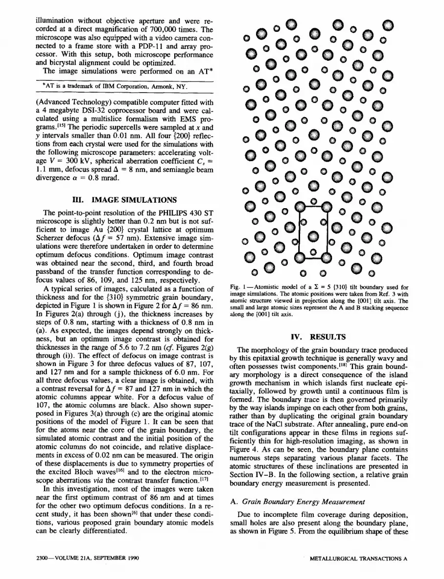
A typical series of images, calculated as a function of thickness and for the {310} symmetric grain boundary, depicted in Figure 1 is shown in Figure 2 for A f = 86 nm. In Figures 2(a) through (j), the thickness increases by steps of 0.8 nm, starting with a thickness of 0.8 nm in (a). As expected, the images depend strongly on thick- ness, but an optimum image contrast is obtained for thicknesses in the range of 5.6 to 7.2 nm (cf. Figures 2(g) through (i)). The effect of defocus on image contrast is shown in Figure 3 for three defocus values of 87, 107, and 127 nm and for a sample thickness of 6.0 rim. For all three defocus values, a clear image is obtained, with a contrast reversal for A f = 87 and 127 nm in which the atomic columns appear white. For a defocus value of 107, the atomic columns are black. Also shown super- posed in Figures 3(a) through (c) are the original atomic positions of the model of Figure 1. It can be seen that for the atoms near the core of the grain boundary, the simulated atomic contrast and the initial position of the atomic columns do not coincide, and relative displace- ments in excess of 0.02 nm can be measured. The origin of these displacements is due to symmetry properties of the excited Bloch waves t161 and to the electron micro- scope aberrations via the contrast transfer function, t17)
In this investigation, most of the images were taken near the first optimum contrast of 86 nm and at times for the other two optimum defocus conditions. In a re- cent study, it has been shown c6~ that under these condi- tions, various proposed grain boundary atomic models can be clearly differentiated.
oO Oo 0 oO 0 o 0 Oo O 0 ~ 0 ~ v O ~
~ 0 v v o ~ 0 ' ~ ~ 0 O ~ v 0 ~ ~ 0 ~ ~ ~ 0 ~
0 v ~ 0 ~ O ~ V O 0 0 ~ ' oO~ ~ 0 ~
~ 0 ~ 0 ~ 0 ~ ~ 0 O ~ ~ 0 ~ ~ O V ~ ~ 0 ~
OV ~0 v O ~ VO 0 ~ 0 vO 0 0
~176176 oO 0 o 0 Oo oo ;Oo Vo o ol !o o
0 ~ ~0 0 0
0 ~ 0 0 U O Fig. 1--Atomistic model of a • = 5 {310} tilt boundary used for image simulations. The atomic positions were taken from Ref. 3 with atomic structure viewed in projection along the [001l tilt axis. The small and large atomic sizes represent the A and B stacking sequence along the [001] tilt axis.
IV. RESULTS
The morphology of the grain boundary trace produced by this epitaxial growth technique is generally wavy and often possesses twist components, t~sj This grain bound- ary morphology is a direct consequence of the island growth mechanism in which islands first nucleate epi- taxiaUy, followed by growth until a continuous film is formed. The boundary trace is then governed primarily by the way islands impinge on each other from both grains, rather than by duplicating the original grain boundary trace of the NaCI substrate. After annealing, pure end-on tilt configurations appear in these films in regions suf- ficiently thin for high-resolution imaging, as shown in Figure 4. As can be seen, the boundary plane contains numerous steps separating various planar facets. The atomic structures of these inclinations are presented in Section IV-B. In the following section, a relative grain boundary energy measurement is presented.
A. Grain Boundary Energy Measurement
Due to incomplete film coverage during deposition, small holes are also present along the boundary plane, as shown in Figure 5. From the equilibrium shape of these
2300--VOLUME 21A, SEPTEMBER 1990 METALLURGICAL TRANSACTIONS A

Fig. 2 - -S imula ted images of a E = 5 {310} tilt boundary as a function of thickness. From (a) to ( j ) , the thickness increases by 0.8 nm starting at 0.8 nm for (a). Microscope parameters: V = 300 kV, C, = 1.1 mm, a = 0.8 mrad, A = 8 nm, and A f = 86 nm.
holes, the relative grain boundary energy can be mea- sured. This approach is similar in nature to the relative energy measurements described by Moil eta/ . t~9~ of [001] twist boundaries in Cu containing small amorphous SiO2 particles. In our case, however, the ratio of grain bound- ary (7,b) to surface energy (y,) is measured instead of the grain boundary to interface energy. Relative energy values have been obtained in two different ways; by measuring the dihedral angle ~ or from the shape anisot- ropy of the lenticular-shaped hole; 1191 i.e.,
Ygt,/'Ys = 2 cos (a/2) [1]
or from trigonometry, Eq. [1] can be expressed as
2(a z - b z)
Ysb/Ys = (a 2 + b2 ) [2]
where a and b are defined as shown in Figure 5. For
both formulae, surface energy isotropy is assumed, and torque terms are neglected. Altogether, 27 well-defined holes with end-on tilt boundaries annealed in vacuum have been measured, giving rise to an average value of YgJYs = 0.62 --- 0.06. Differences in grain boundary energy between various inclinations are not detectable.
B. Grain Boundary Atomic Structure
As mentioned in Section II, the boundary plane can take any preferred inclination since only the misorien- tation angle is controlled. For the ~ = 5 boundaries, the boundary trace has a wavy appearance, and pronounced faceting along symmetric {310} and asymmetric {430}// {100} has been observed, as shown in Figure 6. Small steps on individual boundary facets are marked by ar- rows. The step heights are 2 • d~20o~ and 5 • dt62o~ for the {430}//{100} and {310} interfaces, respectively. These
METALLURGICAL TRANSACTIONS A VOLUME 21A, SEPTEMBER 1990--2301

(a) Fig. 5--High-resolut ion image of a ~ = 5 tilt boundary containing a lenticular-shaped hole. (See Section I V - A for details.)
(b)
Fig. 6--High-resolut ion image of a ~ = 5 boundary showing micro- faceting along {310} symmetrical and {430}ff{100} asymmetrical in- clinations. Also shown are atomic steps marked by arrows.
(c)
Fig. 3 - -S imula ted images of a ~ = 5 {310} tilt boundary as a func- tion of defocus with (a) 87 nm, (b) 107 nm, and (c) 127 rim. Micro- scopeparameters: V = 300 kV, C, = 1.1 mm, a =0 .8 mrad, A = 8 nm, and t = 6 n m .
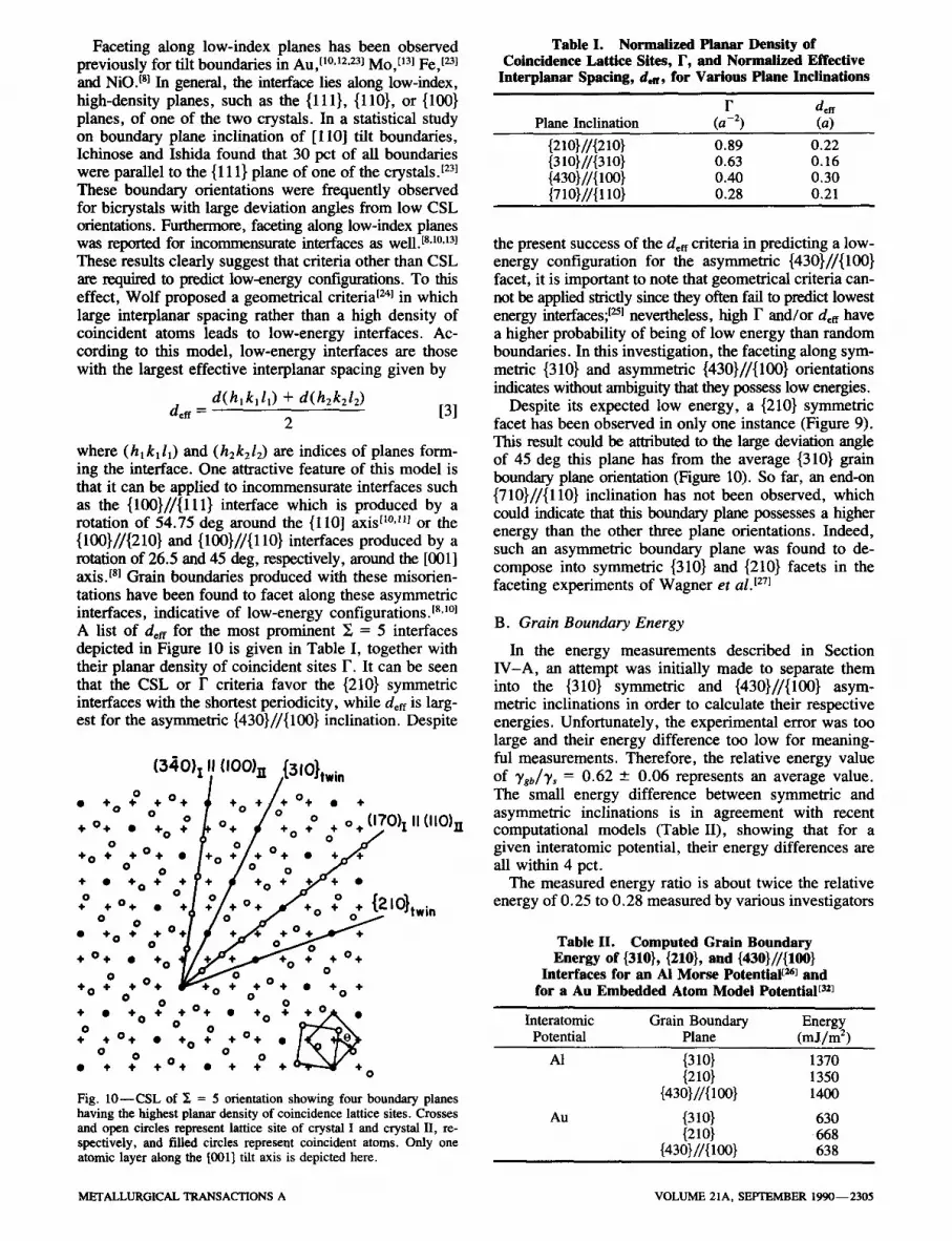
two inclinations have been found frequently and in equal number. In one instance, a {210} symmetric inclination has been observed.
The atomic structure of the {310} symmetric boundary is shown in Figure 7(a) with a possible structural unit, The image periodicity corresponds to the coincidence site lattice (CSL) periodicity of 0.65 nm. This boundary can also be described by a regular array of primary dislo- cations with b = a [100], which gives rise to a localized lattice strain contrast detectable by transmission electron
Fig. 4--High-resolut ion image of a ~ = 5 tilt boundary.
2302--VOLUME 21A, SEPTEMBER 1990 METALLURGICAL TRANSACTIONS A

Fig. 7 - - ( a ) High-resolution image of a symmetrical {310} tiR boundary in Au. Atomic columns are white (Af = 86 ran). (b) Schematic drawing of atomic positions taken from (a) with circles and triangles representing the A and B stacking sequence along the [001] axis separated by a/2 [001].
microscopy (TEM). t2~ In Figure 7(b), an atomic rendi- tion of Figure 7(a) is depicted in which the boundary is described in terms of a regular array of capped triangular prisms, t211 where the core of these dislocations is lo- cated. It is important to note that the dislocation core is empty and that a proposed atomic structure with a filled core containing an additional column of atoms TM has not been observed. In addition, these dislocations remain undissociated.
The atomic structure of the {430}//{100} asymmetric inclination is shown in Figure 8(a). For this boundary, the measured image periodicity of 1.02 nm is half the CSL periodicity of 2.04 nm. The difference arises be- cause in high-resolution electron microscopy (HREM), only the projected potential of atomic columns is con- sidered, without any distinction for the ABAB stacking sequence of (002) planes along the tilt axis. If a specific height is assigned for each atomic column, the boundary CSL periodicity emerges clearly, as can be seen in Figure 8(b). The atomic relaxation of the {200} plane ad- jacent to the core of the core of the grain boundary is important, but the magnitude of this relaxation cannot be measured directly due to the shift between atomic po- sition and image contrast, as described in Section HI.
The atomic structure of the {210} symmetric inclina- tion is shown in Figure 9(a) with a possible structural
unit. The measured image periodicity is 0.46 nm, which is half the CSL periodicity. Similar to the {430}ff{100} interface, the grain boundary periodicity becomes ap- parent whenever a specific stacking sequence is associ- ated with each atomic column, as depicted in Figure 8(b). This boundary plane can be described by a regular array of primary dislocations with b = (a/2) [110] or by an array of capped triangular prisms containing the core of the dislocation. The observed core structure is also empty as for the {310} interface.
Extensive image simulations have been conducted in order to test the detectability of various other computed structures TM with the present microscope. For the con- ditions of optimum defocus and thickness described in Section HI, various models can be clearly distin- guished, t6J Therefore, the HREM results represent a unique structure for each of the three interfaces, and multiplicity in grain boundary structures is not observed.
The volume expansion has been measured for all three boundaries to an accuracy of 0.015 nm by tracing the atomic positions and by measuring the relative lattice displacements from a perfect CSL orientation. For the asymmetrical {430}ff{100} interface, the reference inter- planar spacing between {860} and {200} of crystals I and II, respectively, was taken as the effective spacing; t22j i.e., deff = (dt860} + dt200~)/2, which is equal to 3d{s60}.
METALLURGICAL TRANSACTIONS A VOLUME 21A, SEPTEMBER 1990--2303
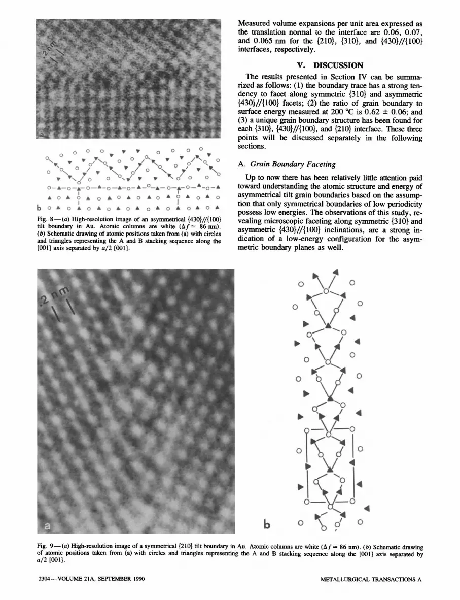
Fig. 8 - - ( a ) High-resolution image of an asymmetrical {430}ff{100} tilt boundary in Au. Atomic columns are white (A f = 86 nm). (b) Schematic drawing of atomic positions taken from (a) with circles and triangles representing the A and B stacking sequence along the [001] axis separated by a/2 [001].
Measured volume expansions per unit area expressed as the translation normal to the interface are 0.06, 0.07, and 0.065 nm for the {210}, {310}, and {430}ff{100} interfaces, respectively.
V. DISCUSSION
The results presented in Section IV can be summa- rized as follows: (1) the boundary trace has a strong ten- dency to facet along symmetric {310} and asymmetric {430}//{100} facets; (2) the ratio of grain boundary to surface energy measured at 200 ~ is 0.62 -+ 0.06; and (3) a unique grain boundary structure has been found for each {310}, {430}//{100}, and {210} interface. These three points will be discussed separately in the following sections.
A. Grain Boundary Faceting
Up to now there has been relatively little attention paid toward understanding the atomic structure and energy of asymmetrical tilt grain boundaries based on the assump- tion that only symmetrical boundaries of low periodicity possess low energies. The observations of this study, re- vealing microscopic faceting along symmetric {310} and asymmetric {430}ff{100} inclinations, are a strong in- dication of a low-energy configuration for the asym- metric boundary planes as well.
Fig. 9 - - ( a ) High-resolution image of a symmetrical {210} tilt boundary in Au. Atomic columns are white (Af --- 86 nm). (b) Schematic drawing of atomic positions taken from (a) with circles and triangles representing the A and B stacking sequence along the [001] axis separated by a/2 [001].
2304--VOLUME 21A, SEPTEMBER 1990 METALLURGICAL TRANSACTIONS A
Faceting along low-index planes has been observed previously for tilt boundaries in A u , [10'12'231 MO, [131 Fe, [23] and NiO. ts] In general, the interface lies along low-index, high-density planes, such as the {111}, {110}, or {100} planes, of one of the two crystals. In a statistical study on boundary plane inclination of [110] tilt boundaries, Ichinose and Ishida found that 30 pet of all boundaries were parallel to the {111} plane of one of the crys ta ls . [231 These boundary orientations were frequendy observed for bicrystals with large deviation angles from low CSL orientations. Furthermore, faceting along low-index planes was reported for incommensurate interfaces as well. ]s'l~ These results clearly suggest that criteria other than CSL are required to predict low-energy configurations. To this effect, Wolf proposed a geometrical criteria [24j in which large interplanar spacing rather than a high density of coincident atoms leads to low-energy interfaces. Ac- cording to this model, low-energy interfaces are those with the largest effective interplanar spacing given by
d(hlklll) + d(h2k212) daf = [3]
2
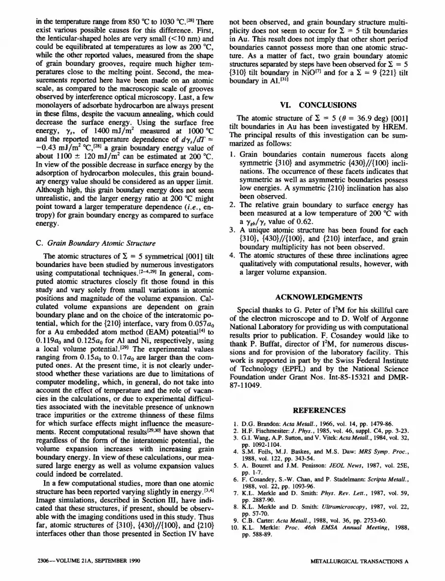
where (h lk~l l ) and (h2k212) are indices of planes form- ing the interface. One attractive feature of this model is that it can be applied to incommensurate interfaces such as the {100}if{l 1 l} interface which is produced by a rotation of 54.75 deg around the {I 10] axis f2~ or the {100}if{210} and {100}if{110} interfaces produced by a rotation of 26.5 and 45 deg, respectively, around the [001] axis. tsl Grain boundaries produced with these misorien- tations have been found to facet along these asymmetric interfaces, indicative of low-energy configurations, ts,l~ A list of dae for the most prominent I~ = 5 interfaces depicted in Figure 10 is given in Table I, together with their planar density of coincident sites F. It can be seen that the CSL or F criteria favor the {210} symmetric interfaces with the shortest periodicity, while d~ff is larg- est for the asymmetric {430}ff{100} inclination. Despite
1340) I O00)a " .{31o},.i. o o l / + o+ �9 �9 4. 0 4. 4- .IF 4- 0 4- +
o O / , o § / o o § o . o . r o / ,o o " J
o o i . o y:~ 4" 0 "l- g "11" �9
:o: :of<i:o,.O. o /: o. .o : o o
�9 +0 + g O
+ o + . . o + o+
+o: . o . 0. o o o o o +
+ a + o + + o + �9 4 0 .i. + o A e o o o
4. 4 O+ �9 +0 + § O+ 0 0 0 0 0
�9 + 4" 4- 4 �9 + + 4, ~ 4 o
Fig. IO- -CSL of l~ = 5 orientation showing four boundary planes having the highest planar density of coincidence lattice sites. Crosses and open circles represent lattice site of crystal I and crystal II, re- s p e c t i v e l y , and filled circles represent coincident atoms. Only one atomic layer along the [001] tilt axis is depicted here.
Table I. Normalized Planar Density of Coincidence Lattice Sites, U, and Normalized Effective
lnterplanar Spacing, din, for Various Plane Inclinations
r a~. Plane Inclination ( a - z) ( a )
{210}ff{210} 0.89 0.22 {310}///310} 0.63 0.16 {430}ff{100} 0.40 0.30 {710}//{110} 0.28 0.21
the present success of the d~ff criteria in predicting a low- energy configuration for the asymmetric {430}//{100} facet, it is important to note that geometrical criteria can- not be applied strictly since they often fail to predict lowest energy interfaces; [zS] nevertheless, high F and/or daf have a higher probability of being of low energy than random boundaries. In this investigation, the faceting along sym- metric {310} and asymmetric {430}//{100} orientations indicates without ambiguity that they possess low energies.
Despite its expected low energy, a {210} symmetric facet has been observed in only one instance (Figure 9). This result could be attributed to the large deviation angle of 45 deg this plane has from the average {310} grain boundary plane orientation (Figure 10). So far, an end-on {710}//{110} inclination has not been observed, which could indicate that this boundary plane possesses a higher energy than the other three plane orientations. Indeed, such an asymmetric boundary plane was found to de- compose into symmetric {310} and {210} facets in the faceting experiments of Wagner e ta / . t271
B. Grain Boundary Energy
In the energy measurements described in Section IV-A, an attempt was initially made to separate them into the {310} symmetric and {430}ff{100} asym- metric inclinations in order to calculate their respective energies. Unfortunately, the experimental error was too large and their energy difference too low for meaning- ful measurements. Therefore, the relative energy value of Ysb/Ys = 0.62 ----- 0.06 represents an average value. The small energy difference between symmetric and asymmetric inclinations is in agreement with recent computational models (Table II), showing that for a given interatomic potential, their energy differences are all within 4 pct.
The measured energy ratio is about twice the relative energy of 0.25 to 0,28 measured by various investigators
Table II. Computed Grain Boundary Energy of {310}, {210}, and {430}//{100}
Interfaces for an AI Morse Potential E261 and for a Au Embedded Atom Model Potential E32]
Interatomic Grain Boundary Energy Potential Plane (mJ/m 2)
A1 {310} 1370 {210} 1350
{430}ff{100} 1400
Au {310} 630 {210} 668
1430}ff{100} 638
METALLURGICAL TRANSACTIONS A VOLUME 21A, SEPTEMBER 1990--2303
in the temperature range from 850 ~ to 1030 ~ t28] There exist various possible causes for this difference. First, the lenticular-shaped holes are very small (< 10 nm) and could be equilibrated at temperatures as low as 200 ~ while the other reported values, measured from the shape of grain boundary grooves, require much higher tem- peratures close to the melting point. Second, the mea- surements reported here have been made on an atomic scale, as compared to the macroscopic scale of grooves observed by interference optical microscopy. Last, a few monolayers of adsorbate hydrocarbon are always present in these films, despite the vacuum annealing, which could decrease the surface energy. Using the surface free energy, 3's, of 1400mJ/m 2 measured at 1000~ and the reported temperature dependence of dys /dT = -0.43 mJ/m 2 ~ t28] a grain boundary energy value of about 1100 _ 120 mJ/m 2 can be estimated at 200 ~ In view of the possible decrease in surface energy by the adsorption of hydrocarbon molecules, this grain bound- ary energy value should be considered as an upper limit. Although high, this grain boundary energy does not seem unrealistic, and the larger energy ratio at 200 ~ might point toward a larger temperature dependence (i.e., en- tropy) for grain boundary energy as compared to surface energy.
C. Grain Boundary Atomic Structure
The atomic structures of E = 5 symmetrical [001] tilt boundaries have been studied by numerous investigators using computational techniques, t2-4,29] In general, com- puted atomic structures closely fit those found in this study and vary solely from small variations in atomic positions and magnitude of the volume expansion. Cal- culated volume expansions are dependent on grain boundary plane and on the choice of the interatomic po- tential, which for the {210} interface, vary from 0.057a0 for a Au embedded atom method (EAM) potentialt4j to 0.119a0 and 0.125a0 for A1 and Ni, respectively, using a local volume potential. [29j The experimental values ranging from 0.15a0 to 0.17a0 are larger than the com- puted ones. At the present time, it is not clearly under- stood whether these variations are due to limitations of computer modeling, which, in general, do not take into account the effect of temperature and the role of vacan- cies in the calculations, or due to experimental difficul- ties associated with the inevitable presence of unknown trace impurities or the extreme thinness of these films for which surface effects might influence the measure- ments. Recent computational results t29,3~ have shown that regardless of the form of the interatomic potential, the volume expansion increases with increasing grain boundary energy. In view of these calculations, our mea- sured large energy as well as volume expansion values could indeed be correlated.
In a few computational studies, more than one atomic structure has been reported varying slightly in energy. [3,4] Image simulations, described in Section III, have indi- cated that these structures, if present, should be observ- able with the imaging conditions used in this study. Thus far, atomic structures of {310}, {430}//{100}, and {210} interfaces other than those presented in Section IV have
not been observed, and grain boundary structure multi- plicity does not seem to occur for ~ = 5 tilt boundaries in Au. This result does not imply that other short period boundaries cannot possess more than one atomic struc- ture. As a matter of fact, two grain boundary atomic structures separated by steps have been observed for ~ = 5 {310} tilt boundary in NiO t7] and for a 'Y. = 9 {221} tilt boundary in A1. [31J
VI. CONCLUSIONS
The atomic structure of Y~ = 5 (0 = 36.9 deg) [001] tilt boundaries in Au has been investigated by HREM. The principal results of this investigation can be sum- marized as follows:
1. Grain boundaries contain numerous facets along symmetric {310} and asymmetric {430}//{100} incli- nations. The occurrence of these facets indicates that symmetric as well as asymmetric boundaries possess low energies. A symmetric {210} inclination has also been observed.
2. The relative grain boundary to surface energy has been measured at a low temperature of 200 ~ with a Ygb/Y, value of 0.62.
3. A unique atomic structure has been found for each {310}, {430}//{100}, and {210} interface, and grain boundary multiplicity has not been observed.
4. The atomic structures of these three inclinations agree qualitatively with computational results, however, with a larger volume expansion.
ACKNOWLEDGMENTS
Special thanks to G. Peter of I2M for his skillful care of the electron microscope and to D. Wolf of Argonne National Laboratory for providing us with computational results prior to publication. F. Cosandey would like to thank P. Buffat, director of I2M, for numerous discus- sions and for provision of the laboratory facility. This work is supported in part by the Swiss Federal Institute of Technology (EPFL) and by the National Science Foundation under Grant Nos. Int-85-15321 and DMR- 87-11049.
REFERENCES
1. D.G. Brandon: Acta Metall., 1966, vol. 14, pp. 1479-86. 2. H.F. Fischmesiter: J. Phys., 1985, vol. 46, suppl. C4, pp. 3-23. 3. G.I. Wang, A.P. Sutton, and V. Vitek: Acta Metall., 1984, vol. 32,
pp. 1092-1104. 4. S.M. Foils, M.J. Baskes, and M.S. Daw: MRS Symp. Proc.,
1988, vol. 122, pp. 343-54. 5. A. Bourret and J.M. Penisson: JEOL News, 1987, vol. 25E,
pp. 1-7. 6. F. Cosandcy, S.-W. Chan, and P. Stadelmann: Scripta Metall.,
1988, vol. 22, pp. 1093-96. 7. K.L. Merklc and D. Smith: Phys. Rev. Lett., 1987, vol. 59,
pp. 2887-90. 8. K.L. Mcrklc and D. Smith: Ultramicroscopy, 1987, vol. 22,
pp. 57-70. 9. C.B. Carter: Acta Metall., 1988, vol. 36, pp. 2753-60.
10. K.L. Merkle: Proc. 46th EMSA Annual Meeting, 1988, pp. 588-89.
2306--VOLUME 21A, SEPTEMBER 1990 METALLURGICAL TRANSACTIONS A

11. H. Norden and D.A. Smith: Proc. 46th EMSA Annual Meeting, 1988, pp. 604-05.
12. F. Cosandey, Y. Komem, and C.L. Bauer: Proc. 9th Int. Conf. on Electron Microscopy, 1978, vol. 1, pp. 434-35.
13. J.M. Penisson: J. Phys., 1988, vol. 49 (C5), pp. 87-97. 14. F. Cosandey, Y. Komem, and C.L. Bauer: Phys. Status Solidi,
1978, vol. 48(a), pp. 555-63. 15. P. Stadelmann: Ultramicroscopy, 1987, vol. 21, pp. 131-46. 16. P. Stadelmann: Int. Phys. Conf. Ser., 1988, vol. 2 (93),
pp. 343-44. 17. A. Bourret, J.L. Rouviere, and J.M. Penisson: Acta Crystallogr.,
1988, vol. A44, pp. 838-47. 18. F. Cosandey and C.L. Bauer: Acta Metall., 1980, vol. 28,
pp. 601-05. 19. T. Mori, H. Miura, T. Takita, J. Haji, and M. Kato: Phil. Mag.
Left., 1988, vol. 58, pp. 11-15. 20. F. Cosandey and C.L. Bauer: Phil. Mag., 1981, vol. A44,
pp. 391-403. 21. V. Vitek, A.P. Sutton, D.A. Smith, and R.C. Pond: in Grain
Boundary Structure and Kinetics, R.W. Balluffi, ed., ASM, Metals Park, OH, 1980, pp. 115-53.
22. K.L. Merkle: Scripta Metall., 1989, vol. 23, pp. 1487-92.
23. H. Iehinose and Y. Ishida: J. Phys., 1985, vol. 46, suppl. C4, pp. 39-49.
24. D. Wolf: J. Phys., 1985, vol. 46, suppl. C4, pp. 197-211. 25. A.P. Sutton and R.W. Balluffi: Acta Metall., 1987, vol. 35,
pp. 2177-2201. 26. D. Wolf: Ceramic Microstructure '86, Role of Interfaces, J.A.
Pask and A.G. Evans, eds., Plenum Press, 1987, vol. 21, pp. 177-89.
27. W.R. Wagner, T.Y. Tan, and R.W. Balluffi: Phil. Mag., 1974, vol. 29, pp. 895-904.
28. L.E. Mutt: lnterfacial Phenomena in Metals and Alloys, 1975, Addison-Wesley, Reading, MA.
29. S.P. Chen, D.J. Srolowitz, and A.F. Voter: J. Mater. Res., 1989, vol. 4, pp. 62-77.
30. D. Wolf, J. Lutsko, and M. Kluge: in Atomistic Simulation of Materials, V. Vitek and D.J. Srolowitz, eds., Plenum Press, 1989, pp. 245-63.
31. M.P. Mills, G.J. Thomas, M.S. Daw, and F. Cosandey: MRS Symp. Proc., 1990, vol. 159, pp. 365-70.
32. D. Wolf: Argonne National Laboratory, Argonne, IL, private communication, 1989.
METALLURGICAL TRANSACTIONS A VOLUME 21A, SEPTEMBER 1990--2307