arohit ee-eco oct112012
TRANSCRIPT
Wavelength agile SWitching in
Photonic integrated circuitS
abhinav rohit
wavelength A
gile Switching in P
hotonic integrated Circuits A
. Rohit
invitation
to attend the public defense of my P
hD thesis entitled
Wavelength a
gile Switching in Photonic integrated c
ircuits
on thursday o
ctober 11, 2012 at 16
:00
hrst
he defense will take place in the A
uditorium of Eindhoven U
niversity of technology.You are also cordially invited to the reception follow
ing the defense.a
bhinav rohit, a.rohit@
tue.nl
Wavelength Agile Switching in PhotonicIntegrated Circuits
PROEFSCHRIFT
ter verkrijging van de graad van doctor aan deTechnische Universiteit Eindhoven, op gezag van derector magnificus, prof.dr.ir. C.J. van Duijn, voor een
commissie aangewezen door het College voorPromoties in het openbaar te verdedigen
op donderdag 11 oktober 2012 om 16.00 uur
door
Abhinav Rohit
geboren te Patna, India

Dit proefschrift is goedgekeurd door de promotor:
prof.dr. H.J.S. Dorren
Copromotor:dr. K.A. Williams
iii
This Ph.D. thesis has been approved by a committee with the follow-ing members:prof.dr. R.V. Penty, University of Cambridge, UKprof.dr.ir. D.van Thourhout, Universiteit Gent, Belgiumprof.dr. M.J. Wale, Eindhoven University of Technology, The Nether-lands
A catalogue record is available from the Eindhoven University of Tech-nology LibraryWavelength Agile Switching in Photonic Integrated CircuitsAuthor: Abhinav RohitEindhoven University of Technology, 2012.ISBN: 978-90-386-3245-2NUR 959
Keywords: Optical fibre communication / Optical switches / Pho-tonic integrated circuits / Semiconductor optical amplifiers / Tunablefilters / Optical resonators / Silicon on insulator technology
The work described in this thesis was performed in the Faculty ofElectrical Engineering of the Eindhoven University of Technology andwas financially supported by the Dutch Technology Foundation, Stift-ing voor Technische Wetenschappen (STW).
Copyright c© 2012 by Abhinav Rohit
All rights reserved. No part of this publication may be reproduced,stored in a retrieval system, or transmitted in any form or by anymeans without the prior written consent of the author.
Typeset using LATEX, printed in The Netherlands

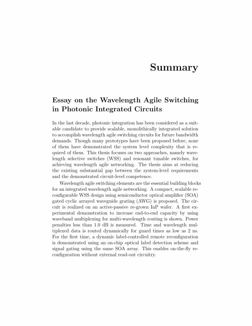
Summary
Essay on the Wavelength Agile Switching
in Photonic Integrated Circuits
In the last decade, photonic integration has been considered as a suit-able candidate to provide scalable, monolithically integrated solutionto accomplish wavelength agile switching circuits for future bandwidthdemands. Though many prototypes have been proposed before, noneof them have demonstrated the system level complexity that is re-quired of them. This thesis focuses on two approaches, namely wave-length selective switches (WSS) and resonant tunable switches, forachieving wavelength agile networking. The thesis aims at reducingthe existing substantial gap between the system-level requirementsand the demonstrated circuit-level competence.
Wavelength agile switching elements are the essential building blocksfor an integrated wavelength agile networking. A compact, scalable re-configurable WSS design using semiconductor optical amplifier (SOA)gated cyclic arrayed waveguide grating (AWG) is proposed. The cir-cuit is realized on an active-passive re-grown InP wafer. A first ex-perimental demonstration to increase end-to-end capacity by usingwaveband multiplexing for multi-wavelength routing is shown. Powerpenalties less than 1.0 dB is measured. Time and wavelength mul-tiplexed data is routed dynamically for guard times as low as 2 ns.For the first time, a dynamic label-controlled remote reconfigurationis demonstrated using an on-chip optical label detection scheme andsignal gating using the same SOA array. This enables on-the-fly re-configuration without external read-out circuitry.
ii
The experimentally verified WSS architecture is combined with apreceding space switch to realize the first monolithically integrated4×4 space and wavelength cross-connect. It combines a broadcastand select stage with the four WSSs. The cross-connect is designedto achieve simultaneous routing of any wavelength from a given in-put port to any given output port. For compact design, two differentSOA lengths are used. Using longer SOAs for both stages will resultin higher signal extinction with greater on-chip loss compensation, al-beit at the cost of larger footprint and energy consumption. To meetthe system-level routing requirements, the circuit is thoroughly char-acterized. Multi-path simultaneous routing is demonstrated for bothco- and counter-propagating data with under 1.0 dB power penalty.For the first time, simultaneous multipath routing of three 40 Gb/sinput signal is demonstrated with less than 0.2 dB power penalty formultiple routed channels. Dynamic routing through the integratedcross-connect is presented employing multiple hops with less than 2ns switching to perform the full circuit assessment. The scalability ofthe current architecture may ultimately be limited by the on-chip losscompensation for the broadcast network, and the crosstalk introduceddue to the waveguide crossings in the shuffle network.
The Silicon-on-Insulator (SOI) integration platform is exploitedto achieve further increase in the switch density due to an increasedindex contrast. Cascaded ring-based tunable switches allow simulta-neous enhancement of both bandwidth and switch extinction which isnot possible using first-order single ring based switches. SOI technol-ogy seems more mature for high yield and uniformity due to CMOS-process compatibility and the availability of commercial foundry ser-vice. Nevertheless, nanometer-scale fabrication error across the chipmakes the realization of large switch fabric extremely challenging. Re-silient fifth-order resonant switch is designed for relaxed tolerances.Detailed theoretical study shows that fabrication tolerances are re-laxed considerably through the combination of moderate size direc-tional couplers of up to 20 µm, moderate 350 GHz free spectral rangeresonator design and the use of fifth order resonance. The detailed ex-perimental analysis confirms the theory with 3-dB bandwidth greaterthan 100 GHz measured with extinction ratio better than 30 dB. The
iii
first study on wavelength misalignment tolerance between 10 Gb/srouted data and the resonant wavelength of the switch element is pre-sented. Low power penalty routing is achievable for signal detuningup to ±50 GHz.
The designed fifth-order broadband switch is used to create an on-chip crossbar switch matrix. In order to evaluate the operation ofthe fabricated cross-bar switch with sufficient connectivity and band-width, proof-of-principle routing experiments are performed. Thermaltuning is used for switching. Micro-heater arrays are fabricated whichprovides the wide-tuning range, and compensate for the inter-switchspectral misalignment. A novel matrix addressing wiring scheme isinvestigated to reduce the number of electrodes. Static as well as dy-namic high speed 10 Gb/s optical signal routing is performed for 1×4and 2×2 configuration. A worst case power penalty of less than 1.5dB is measured. This is highly promising for future high-bandwidthintegrated wavelength agile switch fabrics.

Contents
Summary i
1 Introduction 1
1.1 The Optical Age . . . . . . . . . . . . . . . . . . . . . 1
1.2 Wavelength agile switching . . . . . . . . . . . . . . . . 3
1.3 Photonic Integration . . . . . . . . . . . . . . . . . . . 7
1.4 Wavelength agile subsystems . . . . . . . . . . . . . . . 10
1.4.1 AWG based WSS . . . . . . . . . . . . . . . . . 10
1.4.2 MZI based tunable filter . . . . . . . . . . . . . 11
1.4.3 Resonant tunable filter . . . . . . . . . . . . . . 12
1.5 State-of-the-art . . . . . . . . . . . . . . . . . . . . . . 14
1.5.1 Optical Cross-connect Architectures . . . . . . . 16
1.6 Preview of the thesis . . . . . . . . . . . . . . . . . . . 21
1.7 Novel Contributions . . . . . . . . . . . . . . . . . . . . 22
2 Gated Arrayed Waveguide Grating 25
2.1 Introduction . . . . . . . . . . . . . . . . . . . . . . . . 25
2.2 Fast-programmable cyclic wavelength selective switch . 27
2.3 Circuit Analysis . . . . . . . . . . . . . . . . . . . . . . 29
2.4 Static Wavelength multiplexed Data Routing . . . . . . 32
2.5 Dynamic Data Routing . . . . . . . . . . . . . . . . . . 35
2.5.1 Nanosecond programmable routing . . . . . . . 35
2.5.2 Remote optical label-based routing . . . . . . . 38
2.6 Discussion . . . . . . . . . . . . . . . . . . . . . . . . . 42
2.7 Summary . . . . . . . . . . . . . . . . . . . . . . . . . 43

viii CONTENTS
3 Integrated 4×4 Space andWavelength Cross-connect 45
3.1 Introduction . . . . . . . . . . . . . . . . . . . . . . . . 45
3.2 4×4 Space and Wavelength Cross-connect . . . . . . . 46
3.2.1 Architecture . . . . . . . . . . . . . . . . . . . . 46
3.2.2 Design . . . . . . . . . . . . . . . . . . . . . . . 50
3.3 Circuit Characterization . . . . . . . . . . . . . . . . . 52
3.3.1 Optical spectral response . . . . . . . . . . . . . 53
3.3.2 Optical loss . . . . . . . . . . . . . . . . . . . . 54
3.3.3 Optical gain . . . . . . . . . . . . . . . . . . . . 56
3.4 Data Routing . . . . . . . . . . . . . . . . . . . . . . . 57
3.4.1 Multipath routing . . . . . . . . . . . . . . . . . 58
3.4.2 Bi-directional routing . . . . . . . . . . . . . . . 61
3.4.3 Dynamic Routing . . . . . . . . . . . . . . . . . 63
Multi-hop routing . . . . . . . . . . . . . . . . . 66
3.5 High data rate routing at 40 Gb/s . . . . . . . . . . . . 68
3.6 Discussion . . . . . . . . . . . . . . . . . . . . . . . . . 70
3.7 Summary . . . . . . . . . . . . . . . . . . . . . . . . . 71
4 Resilient Higher-order Resonant switch 73
4.1 Introduction . . . . . . . . . . . . . . . . . . . . . . . . 73
4.2 Resilient fifth-order resonator . . . . . . . . . . . . . . 74
4.2.1 Z-transform description . . . . . . . . . . . . . . 75
4.2.2 Impact of coupling coefficient on passband . . . 77
4.2.3 Resilient directional couplers . . . . . . . . . . . 80
4.2.4 Data integrity . . . . . . . . . . . . . . . . . . . 82
4.3 Fabrication . . . . . . . . . . . . . . . . . . . . . . . . 83
4.3.1 Thin-film Heaters . . . . . . . . . . . . . . . . . 84
4.4 Experimental validation . . . . . . . . . . . . . . . . . 86
4.4.1 Measured transfer function . . . . . . . . . . . . 87
4.4.2 Thermal tuning . . . . . . . . . . . . . . . . . . 89
4.4.3 Resilience to wavelength detuning . . . . . . . . 91
4.4.4 Thermo-Optic Switching Speed . . . . . . . . . 92
4.5 Summary . . . . . . . . . . . . . . . . . . . . . . . . . 93

CONTENTS ix
5 Optical Crossbar Switch Matrix 955.1 Introduction . . . . . . . . . . . . . . . . . . . . . . . . 955.2 Crossbar switch design . . . . . . . . . . . . . . . . . . 98
5.2.1 Waveguide crossing . . . . . . . . . . . . . . . . 995.3 Data Routing . . . . . . . . . . . . . . . . . . . . . . . 100
5.3.1 1×4 Routing . . . . . . . . . . . . . . . . . . . 1005.3.2 2×2 Routing . . . . . . . . . . . . . . . . . . . 1035.3.3 Dynamic Routing . . . . . . . . . . . . . . . . . 106
5.4 Discussion . . . . . . . . . . . . . . . . . . . . . . . . . 1095.5 Summary . . . . . . . . . . . . . . . . . . . . . . . . . 109
6 Conclusions 111
References 117
Acronyms 137
List of Publications 139
Acknowledgments 143
Curriculum Vitæ 145

1Introduction
1.1 The Optical Age
The optical fiber network forms the backbone of today’s global com-munication system. Optical cables have been laid across the conti-nents and under the oceans, creating a mesh-network that connectsthe entire world. With the increase in the reach of the Internet overthe last decade and an exponential increase in the number of con-nected devices - both fixed and mobile - that support high definitionvideo [1, 2], social networking [3, 4], and cloud computing [5], amongother things, the burden on the existing optical communication in-frastructure is ever increasing. In short, this exponential increase indemand for greater bandwidth is driven by the insatiable need of usersfor more and more high-speed connectivity.
Figure 1.1 shows the basic optical network structure. It is classi-fied according to the transmission reach and the total carried traffic.The access network is the face of the network as seen by the user.It provides connectivity to both business and residential users, and itcan span up to 100 km. With the increasing deployment of fiber-to-the-home technology [6] to replace the existing copper access networks,the data rate can range from 0.1-1 Gb/s. The metro network connectsdifferent cities within 300 kms and consists of aggregated traffic fromthe interconnecting access nodes. Data rates can reach up to 10 Gb/sper wavelength within the metro ring. The ’Backbone’ or long-haul
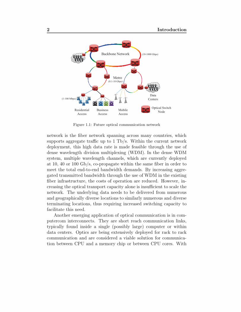
2 Introduction
Residential
Access
Business
Access
Mobile
Access
Data
Centers
Backbone Network
Metro
(1-100 Mbps)
(0.1-10 Gbps)
(10-1000 Gbps)
Optical Switch
Node
Figure 1.1: Future optical communication network
network is the fiber network spanning across many countries, whichsupports aggregate traffic up to 1 Tb/s. Within the current networkdeployment, this high data rate is made feasible through the use ofdense wavelength division multiplexing (WDM). In the dense WDMsystem, multiple wavelength channels, which are currently deployedat 10, 40 or 100 Gb/s, co-propagate within the same fiber in order tomeet the total end-to-end bandwidth demands. By increasing aggre-gated transmitted bandwidth through the use of WDM in the existingfiber infrastructure, the costs of operation are reduced. However, in-creasing the optical transport capacity alone is insufficient to scale thenetwork. The underlying data needs to be delivered from numerousand geographically diverse locations to similarly numerous and diverseterminating locations, thus requiring increased switching capacity tofacilitate this need.
Another emerging application of optical communication is in com-putercom interconnects. They are short reach communication links,typically found inside a single (possibly large) computer or withindata centers. Optics are being extensively deployed for rack to rackcommunication and are considered a viable solution for communica-tion between CPU and a memory chip or between CPU cores. With
1.2 Wavelength agile switching 3
the increasing density of electronic devices on a single CMOS chip,the major factors limiting the bandwidth scalability of the electricalchannels are density of interconnection and energy consumption. Itis the interconnect that accounts for most of the energy dissipation,and that energy is almost all associated with charging and discharg-ing the capacitance of signal lines [7]. In addition to this, skin effect,dielectric losses of transmission lines and reflections due to impedancemismatch in the case of electrical interconnect, limit the data carryingcapacity [8].
Today’s network primarily uses electronic routers. State-of-the-artelectronic routers have already reached capacities over 4 Tb/s withpower consumption of over 13.4 kW [9]. Under these circumstances,scaling of electronic routers to support hundreds of Terabits per sec-ond or even 1 Pb/s becomes extremely difficult. One of the biggestchallenges in moving to all-optical switching is the absence of opticalbuffer or memory and the related issue of synchronization [10]. Us-ing a hybrid approach, in which data processing, buffering, controland scheduling are performed electronically while interconnects andswitching fabrics are implemented in optics, hundreds of terabits persecond is plausible with lower power consumption [11, 12]. Opticalinterconnects can help in overcoming this bottleneck and provides sig-nificantly higher interconnect density and bandwidth-distance productin data and computercom.
1.2 Wavelength agile switching
A crucial component of the network, as shown in Fig. 1.1 is theoptical switch node. It provides the capability to aggregate, disaggre-gate and route data channels in the optical domain. The switchingnodes are shown in Fig. 1.1. The switching nodes have different re-quirements in different sections of the network. At the bottom of thehierarchy, the number of ports in the switch node is larger than inthe case of a backbone network. However, the data rate per channelis much lower. As the data rate increases beyond 40 Gb/s per chan-nel, electronic switches struggle to keep up with the end-to-end band-
4 Introduction
width demands due to increase in power dissipation hot-spots. Opticalswitches provide an advantage of eliminating the optical to electronicconversion required for the electronic counterparts along with provid-ing a line-rate and format transparent switch fabric. Switching theoptical signal in the optical domain eliminates the high-speed elec-tronics in the path which can reduce the complexity of the networkand the associated equipment costs. Hence, there is an increasing needfor fast-programmable, WDM optical switching in telecommunicationsbackbones [13], access networking [14], high performance computingsystems [15] and optical interconnects [16]. This forms the basic moti-vation for this thesis: to propose, design and demonstrate wavelengthagile switching in photonic integrated circuits.There are three ways toachieve wavelength agile routing.
Firstly, fixed wavelength filter with wavelength tunable transmit-ters had been proposed [13, 17] with N×N arrayed waveguide grating(AWG) as router. By tuning the wavelength at each input port, sig-nal can be routed from any input to any output. Although this is thesimplest approach, the switches using this approach are insufficientlyflexible and they require electrically tunable laser with tuning speedwithin tens of nanoseconds. Tunable wavelength conversion at eachAWG input can also be used [18, 19]. However, bandwidth scalabilityis limited with single wavelength operation per port. Alternatively,AWG can be used in a broadcast and select architecture with embed-ded wavelength conversion [13, 20]. Wavelength conversion allows eachwavelength to represent a distinct physical connection albeit increasedpower consumption and hence not favorable for integration.
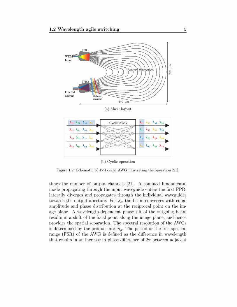
The AWGs are widely used for both multiplexing and de-multiplexingof wavelength channels in WDM networks [21–23]. AWGs work onthe principle of feedforward interference. The AWG consists of threemain parts; multiple input and output waveguides and two identicalfree propagation regions (FPR) which are connected by a waveguidearray. The mask layout of a 4×4 AWG is shown in Fig. 1.2(a).The path difference between adjacent array waveguides is equal tomλc/neff , where m is the order of the array, λc is the central wave-length and neff is the effective refractive index. The number of arms inthe waveguide array, ng, is typically chosen to be about three to four
1.2 Wavelength agile switching 5
WDM
Input
Filtered
Output
FPR1
FPR2
Relative
phase tilt
Arrayed Waveguides
440 m
290
m
(a) Mask layout
12 22 32 42
13 23 33 43
14 24 34 44
21 12 43 34
31 22 13 44
41 32 23 14
11 21 31 41 11 42 33 24Cyclic AWG11 21 31 41
21
31
41
11
(b) Cyclic operation
Figure 1.2: Schematic of 4×4 cyclic AWG illustrating the operation [21].
times the number of output channels [21]. A confined fundamentalmode propagating through the input waveguide enters the first FPR,laterally diverges and propagates through the individual waveguidestowards the output aperture. For λc, the beam converges with equalamplitude and phase distribution at the reciprocal point on the im-age plane. A wavelength-dependent phase tilt of the outgoing beamresults in a shift of the focal point along the image plane, and henceprovides the spatial separation. The spectral resolution of the AWGsis determined by the product m× ng. The period or the free spectralrange (FSR) of the AWG is defined as the difference in wavelengththat results in an increase in phase difference of 2π between adjacent
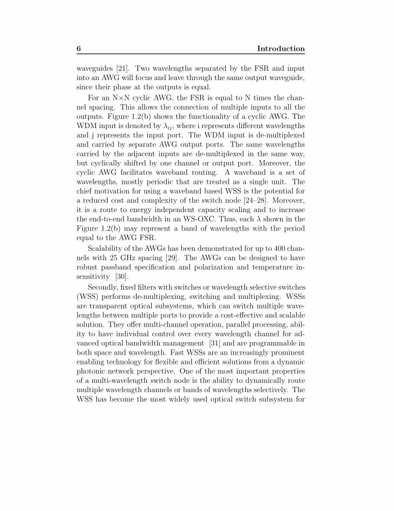
6 Introduction
waveguides [21]. Two wavelengths separated by the FSR and inputinto an AWG will focus and leave through the same output waveguide,since their phase at the outputs is equal.
For an N×N cyclic AWG, the FSR is equal to N times the chan-nel spacing. This allows the connection of multiple inputs to all theoutputs. Figure 1.2(b) shows the functionality of a cyclic AWG. TheWDM input is denoted by λij, where i represents different wavelengthsand j represents the input port. The WDM input is de-multiplexedand carried by separate AWG output ports. The same wavelengthscarried by the adjacent inputs are de-multiplexed in the same way,but cyclically shifted by one channel or output port. Moreover, thecyclic AWG facilitates waveband routing. A waveband is a set ofwavelengths, mostly periodic that are treated as a single unit. Thechief motivation for using a waveband based WSS is the potential fora reduced cost and complexity of the switch node [24–28]. Moreover,it is a route to energy independent capacity scaling and to increasethe end-to-end bandwidth in an WS-OXC. Thus, each λ shown in theFigure 1.2(b) may represent a band of wavelengths with the periodequal to the AWG FSR.
Scalability of the AWGs has been demonstrated for up to 400 chan-nels with 25 GHz spacing [29]. The AWGs can be designed to haverobust passband specification and polarization and temperature in-sensitivity [30].
Secondly, fixed filters with switches or wavelength selective switches(WSS) performs de-multiplexing, switching and multiplexing. WSSsare transparent optical subsystems, which can switch multiple wave-lengths between multiple ports to provide a cost-effective and scalablesolution. They offer multi-channel operation, parallel processing, abil-ity to have individual control over every wavelength channel for ad-vanced optical bandwidth management [31] and are programmable inboth space and wavelength. Fast WSSs are an increasingly prominentenabling technology for flexible and efficient solutions from a dynamicphotonic network perspective. One of the most important propertiesof a multi-wavelength switch node is the ability to dynamically routemultiple wavelength channels or bands of wavelengths selectively. TheWSS has become the most widely used optical switch subsystem for
1.3 Photonic Integration 7
reconfigurable add-drop multiplexers (ROADMs) or wavelength se-lective optical cross-connects (WS-OXC) increasingly deployed in thetelecom network.
Lastly, wavelength agile switching based on tunable wavelength fil-ters have been proposed using Fabry-Perot cavities [32], Bragg gratingfilters [33, 34], phased-array waveguides [35, 36], Mach-Zehnder inter-ferometer (MZI) [37–39] and ring resonators [40, 41]. Circuit-levelimplementation with Fabry-Perot cavities and gratings is challengingdue to the tight fabrication tolerances and intrinsically low number ofoutput ports. Fast-programmable electro-optic phase shifters withindelay-matched arrayed waveguides have enabled excellent widebandunicast routing with up to 16 outputs [42]. However, in terms of scal-ability, simpler control circuitry and usability, MZI and ring resonatorbased tunable filters offer promising prospects for integration.
1.3 Photonic Integration
Photonic integration is the technology of co-fabricating multiple pho-tonic devices on a single monolithic semiconductor wafer. The pho-tonic integrated circuit (PIC) offers a lot of benefits over discrete op-tical system. The total fiber coupling loss and packaging cost canbe reduced as multiple components are combined into a single chip.Other benefits include reduced power consumption and reduced over-all system footprint. Monolithic integration also reduces a significantthermo-electric-energy overhead as the number of temperature con-trolled chips is radically reduced. PICs have been fabricated on avariety of material systems such as silica on silicon (PLC) [43–45],Lithium Niobate [46], SiO2/Si3N4 [47], Silicon on insulator (SOI) [48]and III-V semiconductors [49, 50]. Each material system has its ad-vantages and disadvantages. Figure 1.3 shows the device cross-sectionof the three most widely investigated integration platforms, namelyPLC, Indium Phosphide (InP) and SOI.
A high-refractive index core ridge structure surrounded by low re-fractive index cladding allows light to be guided in the integratedwaveguide by total internal reflection. Higher refractive index con-
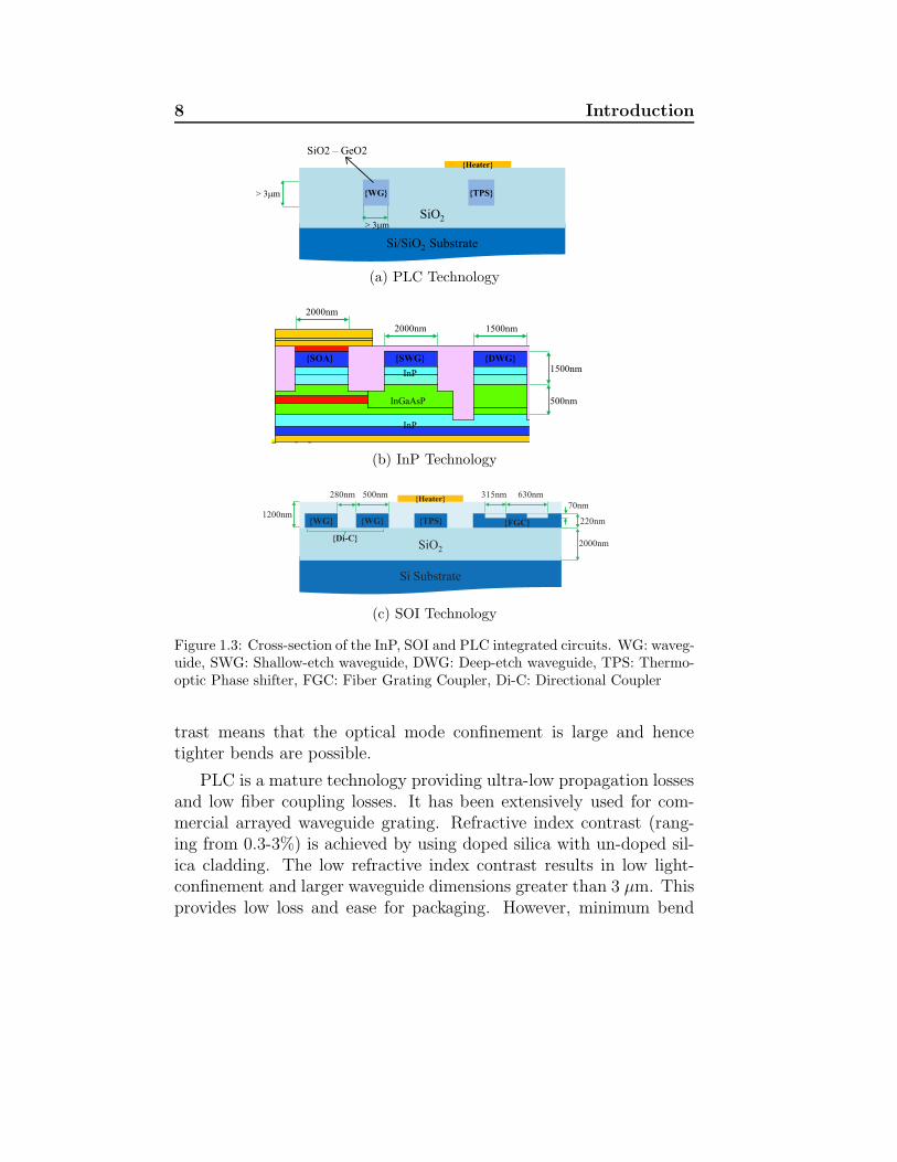
8 Introduction
> 3 m
Si/SiO2 Substrate
SiO2
WG TPS
Heater
SiO2 – GeO2
> 3 m
(a) PLC Technology
500nm
1500nm
InGaAsP
InP
InP
1500nm2000nm
2000nm
SWGSOA DWG
(b) InP Technology
Si Substrate
SiO2
WG WG FGC 220nm
630nm315nm
70nm
500nm280nm
1200nm
Di-C
TPS
Heater
2000nm
(c) SOI Technology
Figure 1.3: Cross-section of the InP, SOI and PLC integrated circuits. WG: waveg-uide, SWG: Shallow-etch waveguide, DWG: Deep-etch waveguide, TPS: Thermo-optic Phase shifter, FGC: Fiber Grating Coupler, Di-C: Directional Coupler
trast means that the optical mode confinement is large and hencetighter bends are possible.
PLC is a mature technology providing ultra-low propagation lossesand low fiber coupling losses. It has been extensively used for com-mercial arrayed waveguide grating. Refractive index contrast (rang-ing from 0.3-3%) is achieved by using doped silica with un-doped sil-ica cladding. The low refractive index contrast results in low light-confinement and larger waveguide dimensions greater than 3 µm. Thisprovides low loss and ease for packaging. However, minimum bend
1.3 Photonic Integration 9
radius of 2 mm results in large device size and hence PLC is not con-sidered in this work.
The InP technology provides a challenging yet multi-functionalplatform for high circuit complexity because of the ability to integrateboth active and passive devices on a single monolithic chip. It can pro-vide light emission, amplification, modulation and detection, all on asingle chip to enable key high-speed high-complexity opto-electroniccircuits. There are three basic elements available on the InP plat-form, namely optical waveguides, phase modulator and semiconduc-tor optical amplifier (SOA). Multiple circuit and system functionali-ties can be derived by using different combinations of these buildingelements [50]. The cost and packaging challenges can be tackled byfollowing a generic foundry approach [51]. In the InP technology1,500 nm thick higher-index quaternary InGaAsP layer is sandwichedbetween InP cladding layers. The deep etched waveguides have largelateral mode confinement allowing low bend radius down to 100 µmand therefore reducing the circuit size. Single mode operation is en-sured in the shallow and deep etched waveguide by using a width of2.0 µm and 1.5 µm respectively. End-fire coupling is used to couplelight in and out of the chip using lensed fibers.
SOI technology uses silicon waveguides on top of a buried silicondioxide layer acting as a lower cladding layer. High index contrast inSOI is preferable for high density and low footprint passive photoniccircuits. Bend radius down to 2 µm is possible with waveguide widthof 500 nm. The SOI technology exploits the mature CMOS foundryprocess to achieve high linewidth uniformity of better than 2.6 nmover a 200 nm wafer [52] for 193 nm deep-UV optical lithographyprocess. Due to the indirect bandgap, active functionality in Si is stillan ongoing research topic. Using highly n-doped Ge-on-Si, researchershave recently demonstrated lasing at room temperature albeit with avery high injected current density [53]. A hybrid approach of a III-V laser bonded to a Si waveguide is one of the feasible solutions tothis problem [54]. Also, the absence of gain in Si means that theswitching elements need to be interferometric, due to the absence ofgain. A thermo-optic phase shift is achievable by locally heating a
1Specific to the JePPIX platform [51] exploited in this thesis

10 Introduction
waveguide using overlying thin-film heaters. Surface coupled gratingor fiber grating coupler (FGC) provides off-chip coupling to and from asingle mode fiber. Table 1.1 summarizes PLC, InP and SOI integrationplatform in terms of component level performance and feasibility.
Table 1.1: Integration Technologies: Indium Phosphide, Silicon-on-insulator and Silica on Silica (PLC)
Building blockPerformance Legend
InP SOI PLC
Passive components X XX XXX
⊖ ChallengingX ModestXX GoodXXX Very Good
Lasers XXX ⊖ ⊖Modulators XXX XX X
Switches XXX XXX X
Optical amplifiers XXX ⊖ ⊖Detectors XXX XXX ⊖Footprint XX XXX X
Chip cost X XX XX
CMOS compatibility ⊖⊖ XX ⊖Low cost packaging ⊖ ⊖1/XX2 XXX1
1Endfire coupling (low reflection)2Vertical coupling (medium reflection)
*InP and SOI comparison taken from Prof. Meint Smit’s Invited talk, OFC2012
1.4 Wavelength agile subsystems
1.4.1 AWG based WSS
Fast reconfigurability in an AWG can be introduced through eitherSOA gate arrays or electro-optic phase tuning. Fast-programmableelectro-optic phase shifters within delay-matched arrayed waveguideshave enabled excellent wideband unicast routing with up to 1×16 out-puts [42, 55, 56]. However, control complexity and energy consumptionincreases with increasing port-count. Alternatively, monolithically in-
1.4 Wavelength agile subsystems 11
tegrated designs based on AWGs and SOAs allow digital control andhave been demonstrated with increasingly impressive levels of connec-tivity with reduced number of SOA gates [35, 57] and scaling up tohundreds of connections [36, 58].
1.4.2 MZI based tunable filter
L
Splitter Combiner
Phase Shifter
FSR
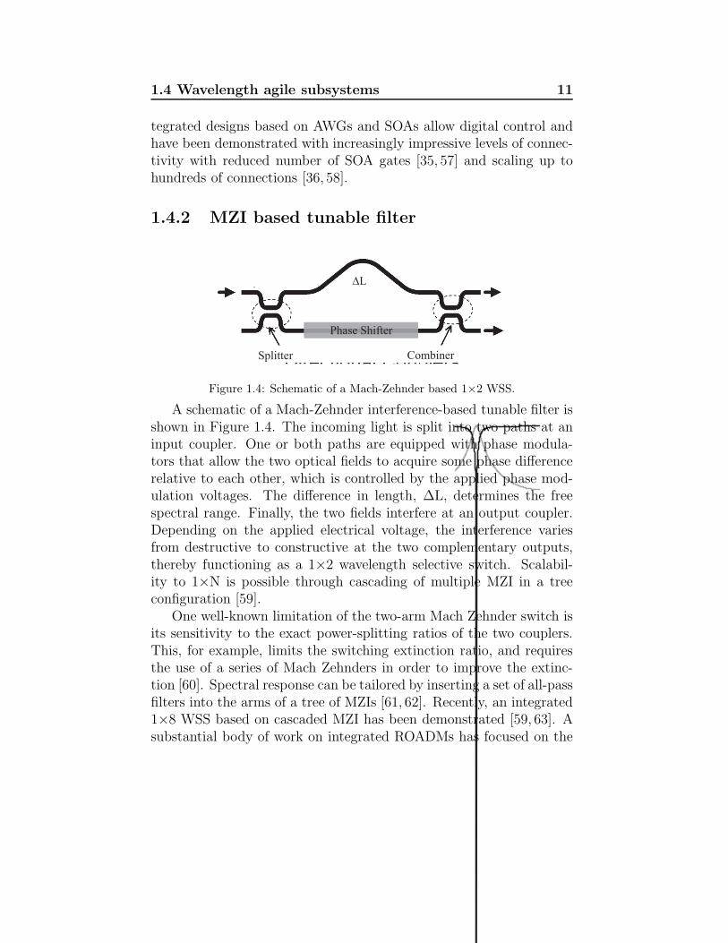
Figure 1.4: Schematic of a Mach-Zehnder based 1×2 WSS.
A schematic of a Mach-Zehnder interference-based tunable filter isshown in Figure 1.4. The incoming light is split into two paths at aninput coupler. One or both paths are equipped with phase modula-tors that allow the two optical fields to acquire some phase differencerelative to each other, which is controlled by the applied phase mod-ulation voltages. The difference in length, ∆L, determines the freespectral range. Finally, the two fields interfere at an output coupler.Depending on the applied electrical voltage, the interference variesfrom destructive to constructive at the two complementary outputs,thereby functioning as a 1×2 wavelength selective switch. Scalabil-ity to 1×N is possible through cascading of multiple MZI in a treeconfiguration [59].
One well-known limitation of the two-arm Mach Zehnder switch isits sensitivity to the exact power-splitting ratios of the two couplers.This, for example, limits the switching extinction ratio, and requiresthe use of a series of Mach Zehnders in order to improve the extinc-tion [60]. Spectral response can be tailored by inserting a set of all-passfilters into the arms of a tree of MZIs [61, 62]. Recently, an integrated1×8 WSS based on cascaded MZI has been demonstrated [59, 63]. Asubstantial body of work on integrated ROADMs has focused on the
12 Introduction
use of MZI-based switches in combination with AWGs as the wave-length multiplexer/de-multiplexer [37–39]. However, the total greaterpower consumption compared to resonant filters, large footprint andlimited extinction ratio of these integrated circuits limits their scala-bility. The MZI based tunable wavelength selective filter is not con-sidered in this thesis for this reason. However, there is ongoing workthat is attempting to improve the extinction ratios and electrical driverresponse of MZI switches in order to enable the high-extinction anddigital response [64] that is required for high connectivity switches.
1.4.3 Resonant tunable filter
-25
-20
-15
-10
-5
0
-0.5 0 0.5
Lo
ss (
dB
)
FSR
Phase
shifterPhase
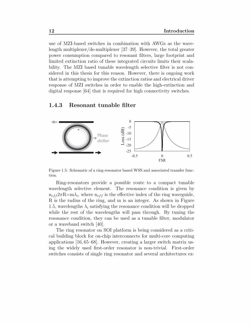
Figure 1.5: Schematic of a ring-resonator based WSS and associated transfer func-tion.
Ring-resonators provide a possible route to a compact tunablewavelength selective element. The resonance condition is given byneff2πR=mλi, where neff is the effective index of the ring waveguide,R is the radius of the ring, and m is an integer. As shown in Figure1.5, wavelengths λi satisfying the resonance condition will be droppedwhile the rest of the wavelengths will pass through. By tuning theresonance condition, they can be used as a tunable filter, modulatoror a waveband switch [40].
The ring resonator on SOI platform is being considered as a criti-cal building block for on-chip interconnects for multi-core computingapplications [16, 65–68]. However, creating a larger switch matrix us-ing the widely used first-order resonator is non-trivial. First-orderswitches consists of single ring resonator and several architectures ex-
1.4 Wavelength agile subsystems 13
ploiting these switches have been proposed [65, 69–78]. Up to 12.5Gb/s signal routing has been demonstrated using switches with 3-dBbandwidth of 38 GHz [77, 78] but with off-state signal extinction ra-tios of only -8 dB and -16 dB. High-Q electronically-tuned micro-ringresonators have also been used for very low switching-energy data-modulators [79], but these devices are designed to operate on narrow-linewidth CW optical signal and to operate with modest extinctionratio. The creation of a large connectivity switch matrices is expectedto require a simultaneous broadening in the on-state signal pass-bandand an increased off-state signal extinction, but simultaneous opti-mization is not feasible for a single order ring-resonator [80]. A closedependence of resonant wavelength on fabricated feature size varia-tions also leads to wavelength errors approaching one nanometer evenfor the state-of-the-art fabrication [52, 80, 81] adding considerable chal-lenges at the circuit level. This makes the first-order resonators verychallenging for large scale switch matrix implementation. In this work,resilient higher-order resonator design consisting of multiple optically-coupled resonators has been used to address and solve this issue.
On the other hand, the current commercially available ROADMsutilize a variety of wavelength agile subsystems [82] such as deflec-tion angle actuator array technologies [83] including micro electro-mechanical systems (MEMS) mirror arrays [84, 85]. These designstypically require calibration over temperature, and they also requirehigh voltage drivers to actuate the MEMS. Other methods include ar-rays of liquid crystal on silicon (LCoS) phase modulators [86]and liquidcrystal (LC) polarization based switches [87]. These typically requirea heater subsystem in order to minimize calibration complexity and tomaintain a minimum switching speed. Phased array designs requirecomplex calculations to determine the desired phase response needinga powerful CPU with the associated power, thermal handling and sizerequirements. Combinations of multiple technologies [88] have alsobeen proposed. To summarize, the MEMS and LCoS based systemscan provide large port-counts and flexible bandwidth [89]. The majorchallenges and drawbacks contributing to the high overall system costinclude high voltage driver requirements, complex control algorithm,thermal handling, aging and opto-mechanical packaging. Moreover,
14 Introduction
switching speed of the order of hundreds of microseconds is expected.The incurring high cost, size and power consumption in these free-space micro-mechanical devices has necessitated the use of photonicintegration technology.
In order to successfully realize a practical wavelength agile circuit,extensive integration is required. In this thesis, the two most promis-ing option for wavelength agile routing, i.e. WSS and resonant tunablefilters are studied for the two most promising integration platforms.
1.5 State-of-the-art
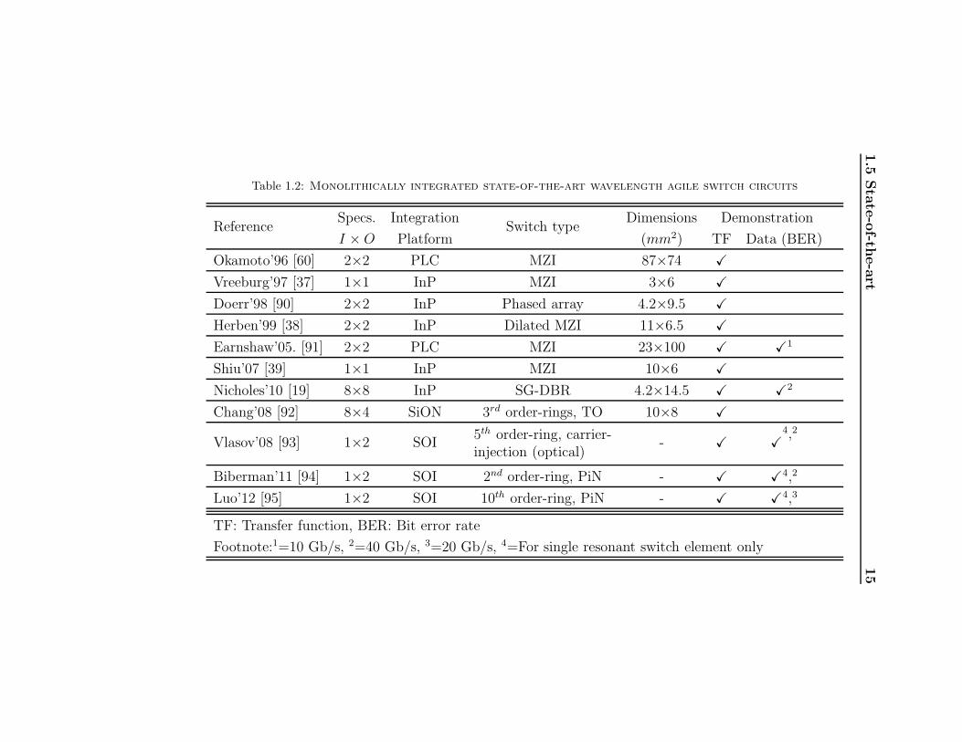
Scalable space- and wavelength-select cross-connect designs have ex-ploited a number of different combinations of wavelength-selectivede/multiplexers, fan-out, fan-in and gating. Prominent experimentally-implemented integrated circuits are compared and contrasted in Table1.2.
The top-half of Table 1.2 shows, in chronological order, the highlysophisticated integrated AWG based WS-OXCs designs found in theliterature. Optoelectronic integrated circuits capable of fast spaceand wavelength selective routing have primarily focused on one WDMinput, one WDM output ROADM concept where wavelengths areswitched to and from colored connections [37–39, 60, 90, 91, 96]. Dueto the inherent complexities of the MZI based designs, the fully in-tegrated wavelength selective OXCs demonstrated have been simple2×2 wavelength switches. Larger N×N wavelength selective OXCshave been proposed from 1×N WSS sub-units. Hence, very limiteddata routing has been demonstrated due to the inherent analogue con-trol complexity and power consumption associated with the MZI basedswitches.
One of the most complicated PIC for wavelength routing proposedis the 8×8 MOTOR circuit [19]. It is fabricated on an active-passiveInP epitaxy and uses on-chip wavelength conversion using sampled-grating distributed Bragg reflector lasers(SG-DBR). This results inlarge single path drive power of ≈2 Watts. This large per path powerconsumption limits the multi-channel operation due to thermal issues.
1.5
State-of-th
e-art
15
Table 1.2: Monolithically integrated state-of-the-art wavelength agile switch circuits
ReferenceSpecs. Integration
Switch typeDimensions Demonstration
I × O Platform (mm2) TF Data (BER)
Okamoto’96 [60] 2×2 PLC MZI 87×74 X
Vreeburg’97 [37] 1×1 InP MZI 3×6 X
Doerr’98 [90] 2×2 InP Phased array 4.2×9.5 X
Herben’99 [38] 2×2 InP Dilated MZI 11×6.5 X
Earnshaw’05. [91] 2×2 PLC MZI 23×100 X X1
Shiu’07 [39] 1×1 InP MZI 10×6 X
Nicholes’10 [19] 8×8 InP SG-DBR 4.2×14.5 X X2
Chang’08 [92] 8×4 SiON 3rd order-rings, TO 10×8 X
Vlasov’08 [93] 1×2 SOI5th order-ring, carrier-injection (optical)
- X X
4,2
Biberman’11 [94] 1×2 SOI 2nd order-ring, PiN - X X4,2
Luo’12 [95] 1×2 SOI 10th order-ring, PiN - X X4,3
TF: Transfer function, BER: Bit error rate
Footnote:1=10 Gb/s, 2=40 Gb/s, 3=20 Gb/s, 4=For single resonant switch element only
16 Introduction
In the bottom half of Table 1.2, higher order resonant switchesbased integrated WS-OXC are listed. Single-order ring based circuitsare not compared here due to the associated challenges discussed be-fore. On-state bandwidth of ≈1 nm is achieved with a higher-orderresonance. A low-penalty transmission of up to 40 Gbit/s signals [93–95] has been demonstrated. Even though larger switch matrices havebeen proposed, data routing demonstrated so far has been limited toa single switch element. The dimension for the single switch elementsare hence omitted from comparison with the demonstrated circuits.The largest switch matrix fabricated so far is an 8×4 matrix con-sisting of third-order resonators [92]. But data routing has not beendemonstrated yet.
1.5.1 Optical Cross-connect Architectures
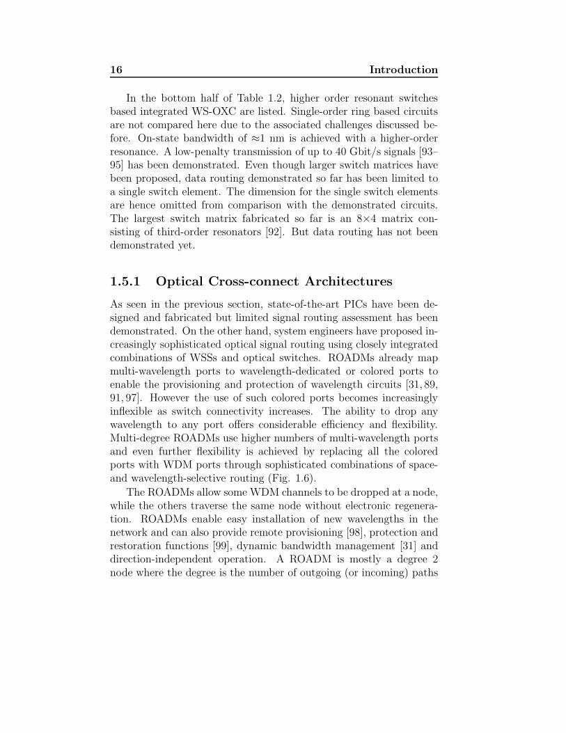
As seen in the previous section, state-of-the-art PICs have been de-signed and fabricated but limited signal routing assessment has beendemonstrated. On the other hand, system engineers have proposed in-creasingly sophisticated optical signal routing using closely integratedcombinations of WSSs and optical switches. ROADMs already mapmulti-wavelength ports to wavelength-dedicated or colored ports toenable the provisioning and protection of wavelength circuits [31, 89,91, 97]. However the use of such colored ports becomes increasinglyinflexible as switch connectivity increases. The ability to drop anywavelength to any port offers considerable efficiency and flexibility.Multi-degree ROADMs use higher numbers of multi-wavelength portsand even further flexibility is achieved by replacing all the coloredports with WDM ports through sophisticated combinations of space-and wavelength-selective routing (Fig. 1.6).
The ROADMs allow some WDM channels to be dropped at a node,while the others traverse the same node without electronic regenera-tion. ROADMs enable easy installation of new wavelengths in thenetwork and can also provide remote provisioning [98], protection andrestoration functions [99], dynamic bandwidth management [31] anddirection-independent operation. A ROADM is mostly a degree 2node where the degree is the number of outgoing (or incoming) paths
1.5 State-of-the-art 17
Bank 2
Route 3
Route 2
PS
PS
PS
PS
PS
PS
Route 1
WSS
WSS
WSS
WSS
WSS
WSS
Transponder Bank 1Bank 3
T/R T/R T/R T/RT/R T/R T/R T/R
Colorless mux/demux Colorless mux/demux Colorless mux/demux
Client-Side Cross Connect
T/R T/R T/R T/R
Figure 1.6: Schematic of a WS-OXC proposed by the AT&T Labs-Research [97].This dynamic photonic node supports 3 inter-node fiber pairs, with colorless andnon-directional add/drop ports.
connected to the node. A multi-degree ROADM (degree greater than2) or a WS-OXC is an extension of the functionality of a ROADM inan optical mesh network. Whereas with the ROADMs, channels areadded and dropped from a single line system for O-E-O conversion,but in the WS-OXC channels are routed in a transparent fashion fromone or more line systems and added to one or more line systems. It canserve up to eight or more fiber routes in a direction independent, color-less operation with full capability for remote reconfiguration [97, 100].Figure 1.6 shows the schematic of such a WS-OXC. It uses power split-ters (PS) and WSS to broadcast and select the appropriate wavelengthsignals for each route and transponder bank. The basic building blockfor such highly flexible WS-OXC is a WSS.
The possibility to define connectivity in terms of the product ofphysical input and the wavelength channel numbers per port allowsorder of magnitude scaling with respect to space switches and wave-length routed switches. This has motivated large scale experimen-tal switch fabric demonstrations for telecom core networks [101–103],metro ring nodes [104–106] and interconnects [15, 107–109]. These ex-
18 Introduction
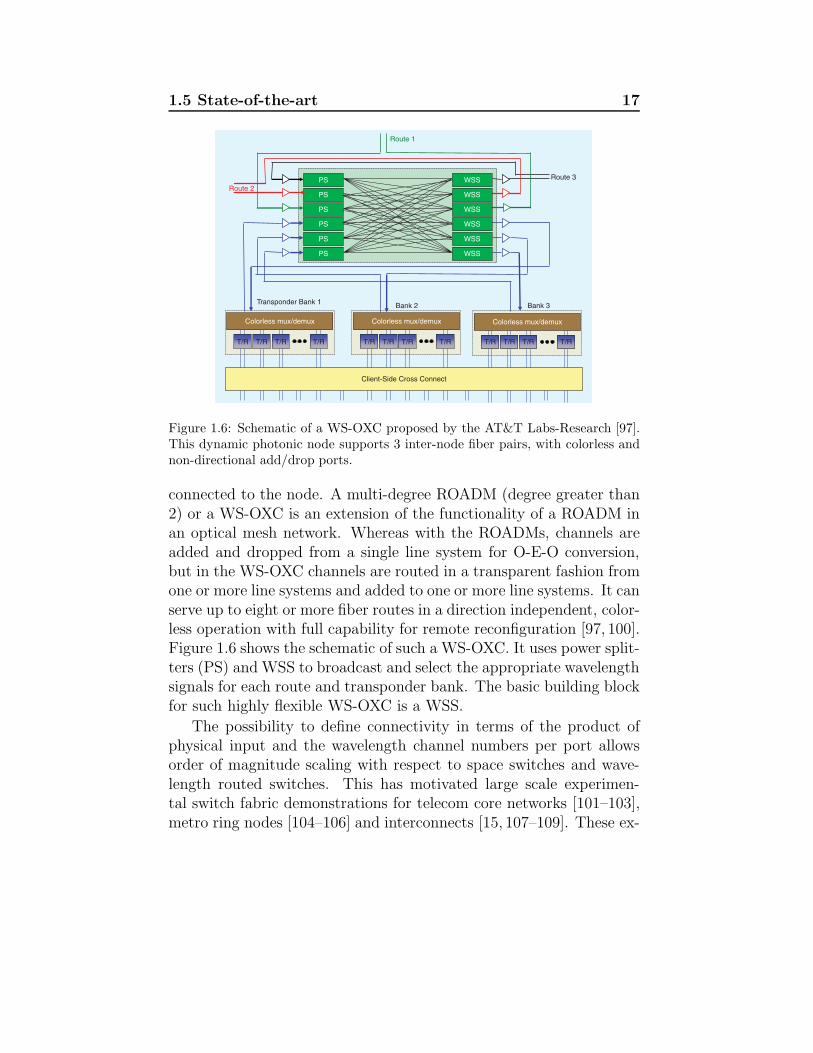
perimental demonstrations have involved nano-second reconfigurableoptical switches and the assembly of very large numbers of separatelyconnectorized photonic components, to create complex multiple rackdemonstrators with complex control. The largest such fully imple-mented fabric has used eight physical inputs and eight wavelengthsper input to enable 64×64 connectivity [108]. Figure 1.7 shows oneout of the 128 optical switching modules used in the implementationhighlighting the attractiveness of photonic integration. Such a combi-nation of space- and wavelength-selective routing allows the numberof connections to be defined by the product of physical input and thewavelength channel numbers. Thus order of magnitude scaling is pos-sible with respect to both space-switch-only [110, 111] and wavelengthrouting [17, 19].
Figure 1.7: Example of a wavelength selection stage using discrete photonic com-ponents consisting of an AWG with eight SOAs [15].
Table 1.3 compares a range of published architectures in termsof component types and the number of each component in brackets.While initial studies considered electro-absorption modulators [101],broad-band SOA gates are now more widely used in system-leveldemonstrators [15, 102–108]. The left-most column highlights the tar-get specifications varying from total connectivity (n2 × n2) of 16×16

1.5
State-of-th
e-art
19
Table 1.3: Space and Wavelength Switching Architectures
Specification Fan out Broadband select Route Wavelength select Fan in Implementation
4λ4 ports in
n × n star (×n) EA gates(×n
2)n × n router (×n) not included not included
Ishida’96 [101]Four paths tested
n2× n
2 shuffle (×1)
16λ16 ports in
n × n star (×n)
SOA gates(×n
3)n × n router (×n
2)SOA gates(×n
3)n × 1 combine (×n
2)Maeno’98 [102]One path tested
n2× n
2 shuffle (×1)
1 × n split (×n)
n2× n
2 shuffle (×n)
16λ16 ports in
n × 1 mux (×n)SOA gates(×n
3)n × n star (×n
2)SOA gates(×n
3)n × 1 mux (×n)
Chiaroni’01 [104]Sub-equipped1 × n split (×n
2)
n3× n
3 shuffle (×n)
16λ16 ports in
n × 1 mux (×n)
SOA gates(×n
3)n × n router (×n
2)SOA gates(×n
3)n × 1 combine (×n
2)Araki’03 [103]One 16λ × 161 space and λ selector
1 × n split (×n)
n2× n
2 shuffle (×1)
1 × n split (×n)
n2× n
2 shuffle (×n)
8λ8 ports in
n × 1 mux (× n)SOA gates(×2n3)
n× 1 combine (×2n2)
1× n demux (× 2n2)
SOA gates(× 2n3)
n × 1 mux (× 2n2)Luijtens’09 [108]Full prototype1 × 2n2 split (×n)
2n2× 2n2 shuffle (×1)
4λ4 ports in
n × 1 mux (× n)SOA gates(× n
2)n × n router (× n)
SOA gates(× n
2)n × 1 combine (× n)1 × n demux (× n)
This work 2012Monolithic(ref. Chapter 3)
1 × n split (×n)
n2× n
2 shuffle (×1)
Comparison for n wavelengths, n physical input ports and total number of wavelength channels n2. The number of wavelengths does not necessarily need to equal
the number of input ports or output ports, although many of the above reports do implement or assume equal numbers.
Key to components:
Multi-wavelength components wavelength selective components implemented with AWG.
n × n star:optical power coupler with n inputsand n outputs
n × n router: cyclic wavelength mapping from n inputs to n outputs.
n × 1 combine: map n inputs to 1 output. n × 1 mux: wavelength multiplex from n colored inputs to one WDM output.
1 × n split: map 1 input to n outputs. 1 × n demux: wavelength demultiplexer from 1 WDM input to n colored outputs.
n × n shuffle:point to point wiring for n inputs andn outputs which require crossings in a2D implementation.
gates: electronically controlled 1 × 1 opticalswitches
20 Introduction
through to 256×256. For ease of comparison here, n wavelengths areassumed for each of the n input connections. A range of arrange-ments of broadband and wavelength specific circuit elements havebeen proposed for fan-out and fan-in. Architectures in Table 1.3mostly implement a two stage selection for broadband-select and finegranularity wavelength-select operations. The input ports connect tofan-outs which require a spatial re-sequencing. This is a non-trivialoperation in integrated circuits and therefore the required shuffle net-works are explicitly listed in Table 1.3. With the exception of thefirst and the last example, the architectures fan out to at least n3
gates. This is n times more gates than connections. This trades re-duced contention for additional photonic circuit complexity as an ad-ditional level of 1×n fan-out, gating, and n×1 fan-in is required. Thetwo selection stages in each architecture allow independent broadbandand wavelength selective gating for the multiple WDM inputs. Thetwo selection stages may be interconnected with arrayed waveguiderouters [101–103], star couplers [104–106] or concatenated combinersand de-multiplexers [15, 107–109]. The choice of wavelength selectivecomponents over broadband components does have important impli-cations for blocking probabilities and signal integrity. For example,the use of a n×n router in place of combiners and splitters may im-pact crosstalk properties and give a significant reduction of opticalloss [103]. The fan-in stages map the gated paths to wavelength mul-tiplexed outputs. The right-most column in Table 1.3 summarizes thelevel of experimentally-implemented complexity.
From Table 1.2 and Table 1.3, it is clear that the functional com-plexity expected from the integrated circuits to meet the current sys-tem requirements has not been demonstrated yet. There is a pressingneed to incorporate and demonstrate a multi-functional integrated so-lution to bridge this gap. It is important for the optical switch fabricto provide broadband operation and simultaneously route high datarate channels over multiple paths.
1.6 Preview of the thesis 21
1.6 Preview of the thesis
This thesis explores the two most promising approaches, namely AWGbased WSS and tunable resonant filter, for high complexity wavelengthagile PICs. These approaches include the broadest range of photonicand optoelectronic components. The challenge is mapping the systemlevel requirements to state-of-the-art integration platforms.
In Chapter Two, a SOA gated AWG is presented as a WSS ele-ment. The fabricated circuit is characterized in terms of the multi-wavelength routing capabilities. A novel on-the-fly self-routing schemeis implemented.
Chapter Three deals with the design and characterization of an in-tegrated 4×4 space and wavelength selective OXC. The circuit perfor-mance is validated for simultaneous multi-path routing, bi-directionalrouting and dynamic reconfigurability. This chapter highlights thefirst multi-functional multi-path routing illustrated for an integratedWS-OXC.
Chapter Four is devoted to thoroughly study and conceive a broad-band resilient higher-order resonant element on SOI platform as acandidate for optical crossbar switch matrix. Quantitative study ispresented to map fabrication-level feature size variation to the op-tical switch performance metrics. Thin-film heaters are fabricated toachieve switching.
Chapter Five serves the purpose of assessing the optical crossbarmatrix formed using the fifth-order resonant switches. Common elec-trical matrix addressing scheme is explored. Performance of the cross-bar switch is evaluated in terms of the measured optical power penaltyfor multiple switched paths. This work represents the first full dataassessment for such crossbar switch implementation.
Finally, Chapter Six presents the conclusion of this work. It ex-plores the relative merits of SOI and InP wavelength agile circuits andcompares them in the context of the desired system level functional-ity.
22 Introduction
1.7 Novel Contributions
1. Demonstration and characterization of the SOA gated cyclicAWG as a WSS element is presented for multi-wavelength dy-namic switch operation. The first demonstration of self-routingis proposed using a monolithic approach to combine optical labelreading and signal gating within a wavelength selective switch.Proof of principle dynamic switching is performed with nanosec-ond time-scale reconfiguration. With a compact chip area of lessthan 5 mm2, this is a highly promising for large-scale wavelength-agile networking.
2. An integrated 4×4 space and wavelength cross-connect has beensuccessfully designed, fabricated and characterized. The firststatic multi-path routing operation was demonstrated for bothco- and counter-propagating 10 Gb/s data channels. For thefirst time, simultaneous routing of three 40 Gb/s input sig-nals is demonstrated for multiple routed channels. Dynamicreconfiguration is shown with nanosecond switching speed us-ing multiple hop routing. This is an important step for in-tegrating next-generation, high-connectivity, high-throughput,dynamically-reconfigurable, optical cross-connects.
3. A fifth-order resonant switch is designed on Silicon-on-insulatorplatform as a resilient broadband tunable wavelength agile switchelement. Variation in the coupling coefficients and their impacton data integrity are presented for the first time as a function offabrication error. Thin-film heater is fabricated for thermo-opticswitching. Large bandwidth is achieved allowing robustnessto wavelength misalignments. The fifth-order resonant switchproves to be a viable candidate for large scale broadband cross-bar switching networks.
4. The fifth-order switch elements are cascaded to form an opticalcrossbar switch matrix. For the first time, data routing is pre-sented for static 1×4 and 2×2 operation as well as dynamicswitch operation in a high-order switch matrix. Data integrity

1.7 Novel Contributions 23
for the routed signal is presented in terms of the circuit levelmetrics of loss, crosstalk and optical power penalty for the mea-sured paths.
5. The author has designed all the PICs presented in this thesisexcept for the one reported in Chapter two. The PICs werefabricated as part of the multi-project wafer process. The post-fabrication step presented in Chapter 4 has been carried outby the author in the TU/e cleanroom under the supervision ofDr. R. Stabile. The author is solely responsible for all themeasurements carried out and presented in this thesis.

2Gated Arrayed Waveguide
Grating
In this chapter1, a compact, scalable and reconfigurable WSS is pro-posed and demonstrated based on a SOA gated AWG. Wavebandrouting is demonstrated exploiting the cyclic property of the AWG.Nanosecond timescale switching speed is achieved. Remote reconfigu-ration is proposed using label detection and signal gating in the sameSOA array. A proof of principle experiment is presented showing dy-namic nanosecond label-controlled switching.
2.1 Introduction
AWGs in combination with SOAs provide a viable architecture foran integrated WSS with a reduced number of gates [35, 36, 57]. TheAWG is promising for scalability to large-port count [35, 36]. Theend-to-end capacity can be further increased by exploiting the cyclicproperty of the AWG and the multi-THz bandwidth of SOAs, signi-fying a route to hardware and energy efficient networking. The SOAsgates provision digital control, fast reconfigurability and on-chip losscompensation. The fast switching speed allows very high optical layerlink utilization. While nanosecond reconfigurability has been demon-
1Based on the results published in [112–115]
26 Gated Arrayed Waveguide Grating
strated previously [116], the impact on data integrity has not beenassessed for the WSS.
Remote on-the-fly reconfigurability is desired for WSS to minimizenetwork delays [31, 88] and to avoid clock recovery at the optical switchelement [117]. Multi-wavelength optical labels have been proposedto reconfigure such WSS sub-systems for packet-switched applications[118–120]. Binary WDM address coding allows a minimum of n opticallabels to control 2n WDM channels. The RF-tone in-band labelingtechnique can further increase the number of channels that can beaddressed per label wavelength [121]. This is feasible with simple,low-speed electronic circuitry. However, many of the WSS solutionsproposed to date assume separate circuit elements for the monitoringof labels and the routing of data. The additional components andsplitters incur hardware complexity, energy loss and link loss. On-chiplabel detection has been studied for switching matrices to simplifyhardware complexity [122], although the implemented scheme doesstill require additional monitors for full circuit operation. The on-chip SOAs can be used both to detect the labels and to gate routedsignals [58, 123].
In this chapter, a gated cyclic AWG is proposed, fabricated andcharacterized as a fast WSS. Fast reconfigurability is enabled by inte-grating SOA gate arrays which operate with simple digital signals. Thecircuit concept is presented in Section 2.2. Component level character-ization is described in Section 2.3. In Section 2.4, low power penaltydata routing is studied for two modes of multi-wavelength operation.Nanosecond re-configurability is analyzed in Section 2.5.1 by meansof full bit error assessment. And lastly in Section 2.5.2 a novel remoteoptical-label controlled switching is demonstrated. The control circuitis explained, and comparative bit error rate measurements with andwithout dynamically reallocated switching states are presented.
2.2 Fast-programmable cyclic wavelength selective switch 27
2.2 Fast-programmable cyclic wavelength
selective switch
The 1×4 WSS is designed to allow the selective routing of bands ofwavelength channels to any of the four outputs. The input signal isbroadcast to the SOA gate array and appropriate electrical biasingof the gates determines the circuit transfer function, allowing multiplewavelengths to be simultaneously routed. Due to the cyclic property ofthe AWG, groups of wavelengths separated by one free spectral rangeare routed to the same output port of the AWG. The mapping of thefour wavebands to each of the four outputs is shown in table 2.1. Thefree spectral range for the presented 4×4 cyclic AWG is five timesthe channel separation, leaving one band unconnected for each freespectral range.
4x4
Cyclic
AWG
SOA gated AWG
SOA gate
1×2 MMI
(a)
(b)
Figure 2.1: SOA gated cyclic AWG (a) Schematic, (b) Mask layer representationshowing waveguides (black lines), deep etch areas (grey zones) and the 750µm longactive region (upper central red zone)
The schematic and the mask layout of the SOA gated AWG isshown in figure 2.1(a) and figure 2.1(b) respectively. The waveguidemask layers and the active island mask are shown highlighting the
28 Gated Arrayed Waveguide Grating
Table 2.1: Routing Map for ON-State Gates
Output Port SOA gate 1 SOA gate 2 SOA gate 3 SOA gate 4
1 Waveband 1 Unconnected Waveband 4 Waveband 3
2 Waveband 2 Waveband 1 Unconnected Waveband 4
3 Waveband 3 Waveband 2 Waveband 1 Unconnected
4 Waveband 4 Waveband 3 Waveband 2 Waveband 1
placement of the input, outputs, enumerated SOA gates and the cyclicAWG. Both shallow and deep etched waveguides are used within thecircuit. The waveguides are highlighted in black, and the regions fordeep etched sidewalls are denoted by the greyed areas. The inputand output waveguides are angled at 7 off facet-normal for reducedreflectivity. A fundamental-spatial-mode filter implemented with a1×1 multimode interference coupler is used to condition the signalpropagating into the circuit. Two stages of 1×2 multimode inter-ference splitters are then used to broadcast the input to each of theSOA gates. Between straight and curved sections, waveguide offsetsare used to minimize mode mismatch. Deeply etched waveguides areused to allow tight bend radii. Tapered transition sections betweendeep-etched and shallow etched circuit elements minimize reflectionsat the interfaces and are implemented at each side of the active island.The SOA gates at the central active island are implemented as low-loss shallow-etched ridge waveguides for improved efficiency. The fourSOA gates each have a length of 140 µm and are angled at 12 relativeto the active island length. These fit within the same compact 30 µm× 750 µm active island and all the circuit elements are accommodatedinto a small area of under 5 mm2 with a total chip length of 4.6 mm.
Fabrication
The circuit is implemented monolithically on a regrown active-passiveInGaAsP/InP epitaxy as part of a JePPIX multi-project wafer run[49]. The active waveguide structure used for the SOA gates in-
2.3 Circuit Analysis 29
cludes four InGaAsP quantum wells within a confinement region oftotal thickness 500 nm. Detailed waveguide structure is shown in fig-ure 1.3(b). The gain in the SOAs is achieved by electrically pumpingthe active region. The incoming light is amplified via stimulated emis-sion. An optical bandwidth greater than 100 nm is feasible which isextremely useful in the WDM systems. The gain spectrum is centeredat a peak wavelength of 1550 nm. The passive waveguide structureconsists of a 500 nm core layer with quaternary composition Q=1.25µm sandwiched between binary InP alloy cladding layers. Shallow anddeep-etched waveguides are defined by a two step reactive ion etch.The first step is performed with the shallow waveguides masked. Deepetch waveguides are used to define the MMI splitters and tight waveg-uide bends. Radii of down to 100 µm are used both for entering thecyclic AWG and within the cyclic AWG itself. End-fire coupling isused to couple light in and out of the chip using lensed fibers. Figure2.2 shows a micrograph composed from detailed Scanning ElectronMicroscope (SEM) images of the device at the central part of the cir-cuit. The cyclic AWG and the SOA gate array are visible along withthe four p-type gate electrodes.
Figure 2.2: SEM image of the circuit showing the cyclic AWG (left) and the SOAgate array (upper right).
2.3 Circuit Analysis
The cyclic AWG is designed with channel spacing of 3.2 nm (400 GHz)and a free spectral range of 16 nm (2 THz). The deep etched arrayed
30 Gated Arrayed Waveguide Grating
-20
-15
-10
-5
0
1.50 1.52 1.54 1.56 1.58 1.60
Tra
nsfe
r F
unct
ion
(dB
)
Wavelength (µm)
Waveband 1 Waveband 2Waveband 3 Waveband 4
(a)
-80
-75
-70
-65
1.50 1.52 1.54 1.56 1.58 1.60Wavelength (µm)S
pont
ane
ousE
mis
sion
(dB
m/0
.1n
m)
(b)
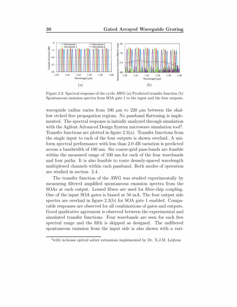
Figure 2.3: Spectral response of the cyclic AWG (a) Predicted transfer function (b)Spontaneous emission spectra from SOA gate 1 to the input and the four outputs.
waveguide radius varies from 100 µm to 220 µm between the shal-low etched free propagation regions. No passband flattening is imple-mented. The spectral response is initially analyzed through simulationwith the Agilent Advanced Design System microwave simulation tool2.Transfer functions are plotted in figure 2.3(a). Transfer functions fromthe single input to each of the four outputs is shown overlaid. A uni-form spectral performance with less than 2.0 dB variation is predictedacross a bandwidth of 100 nm. Six coarse-grid pass-bands are feasiblewithin the measured range of 100 nm for each of the four wavebandsand four paths. It is also feasible to route densely-spaced wavelengthmultiplexed channels within each passband. Both modes of operationare studied in section 2.4.
The transfer function of the AWG was studied experimentally bymeasuring filtered amplified spontaneous emission spectra from theSOAs at each output. Lensed fibres are used for fibre-chip coupling.One of the input SOA gates is biased at 50 mA. The four output sidespectra are overlaid in figure 2.3(b) for SOA gate 1 enabled. Compa-rable responses are observed for all combinations of gates and outputs.Good qualitative agreement is observed between the experimental andsimulated transfer functions. Four wavebands are seen for each freespectral range and the fifth is skipped as designed. The unfilteredspontaneous emission from the input side is also shown with a vari-
2with in-house optical solver extensions implemented by Dr. X.J.M. Leijtens
2.3 Circuit Analysis 31
SOA
Chopper Driver200 Hz
Current Source
Lock–In
LASER
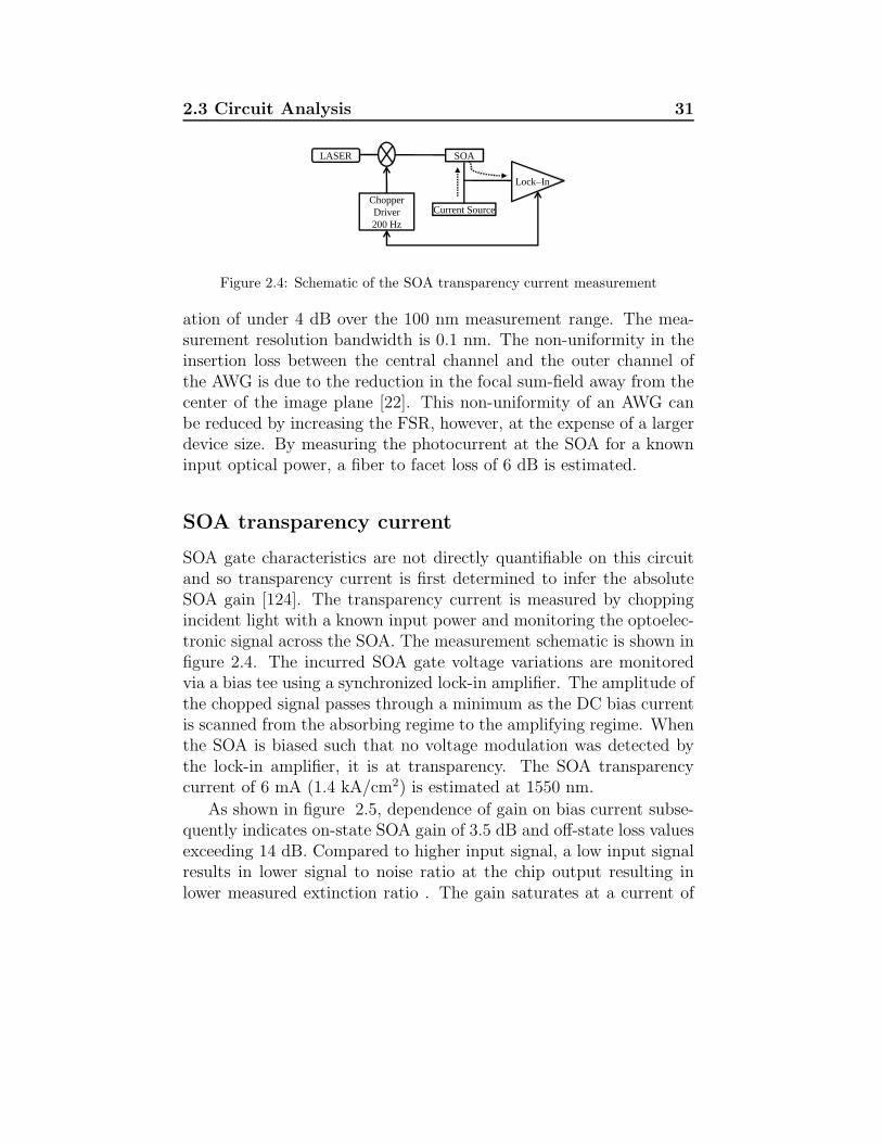
Figure 2.4: Schematic of the SOA transparency current measurement
ation of under 4 dB over the 100 nm measurement range. The mea-surement resolution bandwidth is 0.1 nm. The non-uniformity in theinsertion loss between the central channel and the outer channel ofthe AWG is due to the reduction in the focal sum-field away from thecenter of the image plane [22]. This non-uniformity of an AWG canbe reduced by increasing the FSR, however, at the expense of a largerdevice size. By measuring the photocurrent at the SOA for a knowninput optical power, a fiber to facet loss of 6 dB is estimated.
SOA transparency current
SOA gate characteristics are not directly quantifiable on this circuitand so transparency current is first determined to infer the absoluteSOA gain [124]. The transparency current is measured by choppingincident light with a known input power and monitoring the optoelec-tronic signal across the SOA. The measurement schematic is shown infigure 2.4. The incurred SOA gate voltage variations are monitoredvia a bias tee using a synchronized lock-in amplifier. The amplitude ofthe chopped signal passes through a minimum as the DC bias currentis scanned from the absorbing regime to the amplifying regime. Whenthe SOA is biased such that no voltage modulation was detected bythe lock-in amplifier, it is at transparency. The SOA transparencycurrent of 6 mA (1.4 kA/cm2) is estimated at 1550 nm.
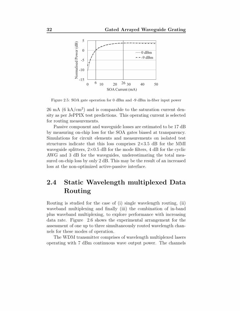
As shown in figure 2.5, dependence of gain on bias current subse-quently indicates on-state SOA gain of 3.5 dB and off-state loss valuesexceeding 14 dB. Compared to higher input signal, a low input signalresults in lower signal to noise ratio at the chip output resulting inlower measured extinction ratio . The gain saturates at a current of
32 Gated Arrayed Waveguide Grating
-15
-10
-5
0
5
0 10 20 30 40 50
No
rmal
ised
Po
wer
(d
B)
SOA Current (mA)
0 dBm
-9 dBm
266
Figure 2.5: SOA gate operation for 0 dBm and -9 dBm in-fiber input power
26 mA (6 kA/cm2) and is comparable to the saturation current den-sity as per JePPIX test predictions. This operating current is selectedfor routing measurements.
Passive component and waveguide losses are estimated to be 17 dBby measuring on-chip loss for the SOA gates biased at transparency.Simulations for circuit elements and measurements on isolated teststructures indicate that this loss comprises 2×3.5 dB for the MMIwaveguide splitters, 2×0.5 dB for the mode filters, 4 dB for the cyclicAWG and 3 dB for the waveguides, underestimating the total mea-sured on-chip loss by only 2 dB. This may be the result of an increasedloss at the non-optimized active-passive interface.
2.4 Static Wavelength multiplexed Data
Routing
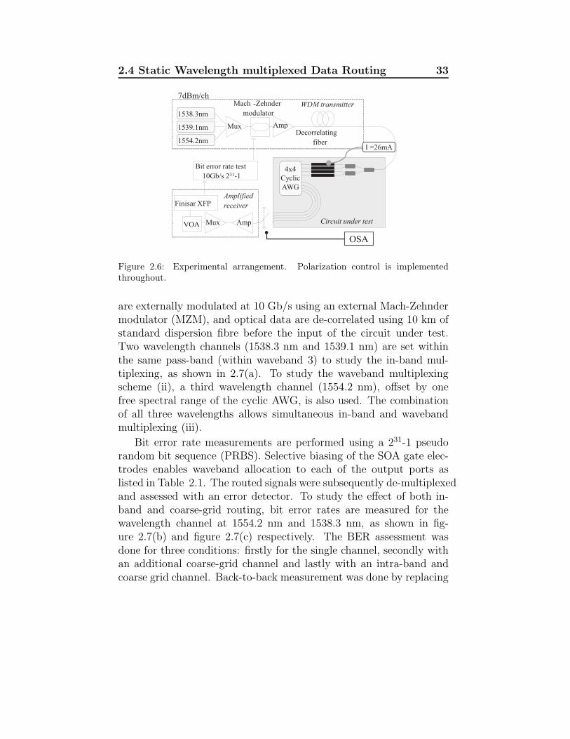
Routing is studied for the case of (i) single wavelength routing, (ii)waveband multiplexing and finally (iii) the combination of in-bandplus waveband multiplexing, to explore performance with increasingdata rate. Figure 2.6 shows the experimental arrangement for theassessment of one up to three simultaneously routed wavelength chan-nels for these modes of operation.
The WDM transmitter comprises of wavelength multiplexed lasersoperating with 7 dBm continuous wave output power. The channels
2.4 Static Wavelength multiplexed Data Routing 33
4x4
Cyclic
AWG
1538.3nm
1539.1nm
1554.2nm
Mux AmpDecorrelating
fiber
AmpMuxVOA
Finisar XFP
Bit error rate test
10Gb/s 231-1
Circuit under test
Mach -Zehnder
modulator
WDM transmitter
Amplified
receiver
OSA
7dBm/ch
I =26mA
Figure 2.6: Experimental arrangement. Polarization control is implementedthroughout.
are externally modulated at 10 Gb/s using an external Mach-Zehndermodulator (MZM), and optical data are de-correlated using 10 km ofstandard dispersion fibre before the input of the circuit under test.Two wavelength channels (1538.3 nm and 1539.1 nm) are set withinthe same pass-band (within waveband 3) to study the in-band mul-tiplexing, as shown in 2.7(a). To study the waveband multiplexingscheme (ii), a third wavelength channel (1554.2 nm), offset by onefree spectral range of the cyclic AWG, is also used. The combinationof all three wavelengths allows simultaneous in-band and wavebandmultiplexing (iii).
Bit error rate measurements are performed using a 231-1 pseudorandom bit sequence (PRBS). Selective biasing of the SOA gate elec-trodes enables waveband allocation to each of the output ports aslisted in Table 2.1. The routed signals were subsequently de-multiplexedand assessed with an error detector. To study the effect of both in-band and coarse-grid routing, bit error rates are measured for thewavelength channel at 1554.2 nm and 1538.3 nm, as shown in fig-ure 2.7(b) and figure 2.7(c) respectively. The BER assessment wasdone for three conditions: firstly for the single channel, secondly withan additional coarse-grid channel and lastly with an intra-band andcoarse grid channel. Back-to-back measurement was done by replacing
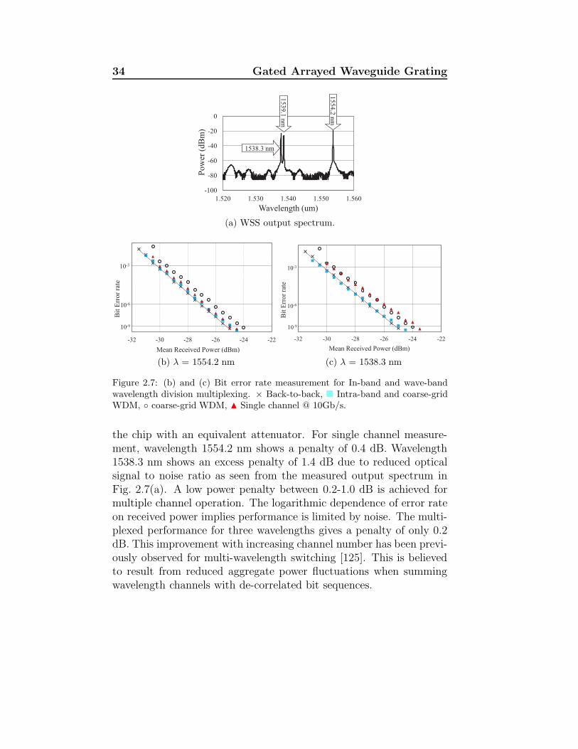
34 Gated Arrayed Waveguide Grating
-100
-80
-60
-40
-20
0
1.520 1.530 1.540 1.550 1.560P
ow
er (
dB
m)
Wavelength (um)
1538.3 nm
15
39
.1 n
m
15
54
.2 n
m
(a) WSS output spectrum.
-32 -30 -28 -26 -24 -22
Bit
Err
or
rate
Mean Received Power (dBm)
10-9
10-3
10-6
(b) λ = 1554.2 nm
-32 -30 -28 -26 -24 -22
Bit
Err
or
rate
Mean Received Power (dBm)
10-9
10-3
10-6
(c) λ = 1538.3 nm
Figure 2.7: (b) and (c) Bit error rate measurement for In-band and wave-bandwavelength division multiplexing. × Back-to-back, Intra-band and coarse-gridWDM, coarse-grid WDM, N Single channel @ 10Gb/s.
the chip with an equivalent attenuator. For single channel measure-ment, wavelength 1554.2 nm shows a penalty of 0.4 dB. Wavelength1538.3 nm shows an excess penalty of 1.4 dB due to reduced opticalsignal to noise ratio as seen from the measured output spectrum inFig. 2.7(a). A low power penalty between 0.2-1.0 dB is achieved formultiple channel operation. The logarithmic dependence of error rateon received power implies performance is limited by noise. The multi-plexed performance for three wavelengths gives a penalty of only 0.2dB. This improvement with increasing channel number has been previ-ously observed for multi-wavelength switching [125]. This is believedto result from reduced aggregate power fluctuations when summingwavelength channels with de-correlated bit sequences.
2.5 Dynamic Data Routing 35
2.5 Dynamic Data Routing
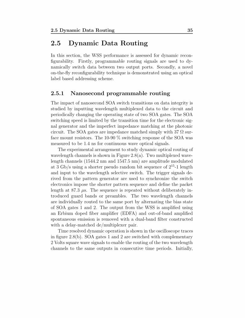
In this section, the WSS performance is assessed for dynamic recon-figurability. Firstly, programmable routing signals are used to dy-namically switch data between two output ports. Secondly, a novelon-the-fly reconfigurability technique is demonstrated using an opticallabel based addressing scheme.
2.5.1 Nanosecond programmable routing
The impact of nanosecond SOA switch transitions on data integrity isstudied by inputting wavelength multiplexed data to the circuit andperiodically changing the operating state of two SOA gates. The SOAswitching speed is limited by the transition time for the electronic sig-nal generator and the imperfect impedance matching at the photoniccircuit. The SOA gates are impedance matched simply with 37 Ω sur-face mount resistors. The 10-90 % switching response of the SOA wasmeasured to be 1.4 ns for continuous wave optical signals.
The experimental arrangement to study dynamic optical routing ofwavelength channels is shown in Figure 2.8(a). Two multiplexed wave-length channels (1544.2 nm and 1547.5 nm) are amplitude modulatedat 3 Gb/s using a shorter pseudo random bit sequence of 215-1 lengthand input to the wavelength selective switch. The trigger signals de-rived from the pattern generator are used to synchronize the switchelectronics impose the shorter pattern sequence and define the packetlength at 87.3 µs. The sequence is repeated without deliberately in-troduced guard bands or preambles. The two wavelength channelsare individually routed to the same port by alternating the bias stateof SOA gates 1 and 2. The output from the WSS is amplified usingan Erbium doped fiber amplifier (EDFA) and out-of-band amplifiedspontaneous emission is removed with a dual-band filter constructedwith a delay-matched de/multiplexer pair.
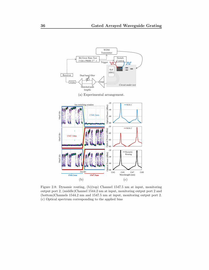
Time resolved dynamic operation is shown in the oscilloscope tracesin figure 2.8(b). SOA gates 1 and 2 are switched with complementary2 Volts square wave signals to enable the routing of the two wavelengthchannels to the same outputs in consecutive time periods. Initially,
36 Gated Arrayed Waveguide Grating
Circuit under testVOA
Bit Error Rate Test
3 Gb/s PRBS 215 -1
Switch
Control
Dual band filter
Matched path
lengths
Receiver
WDM
Transmitter
4x4
AWG
Trigger
Amp
(a) Experimental arrangement.
1544.2nm 1547.5nm
1547.5nm
1544.2nm
1ns switching window
10
mV
/div
10
mV
/div
10
mV
/div
2ns/div
(b)
-80
-60
-40
-20
1543 1545 1547 1549
Op
tica
l Po
wer
(d
Bm
)
Wavelength(nm)
SOA 1
-80
-60
-40
-20
1543 1545 1547 1549
Op
tical
Po
wer
(d
Bm
)
Wavelength(nm)
SOA 2
-80
-60
-40
-20
1543 1545 1547 1549
Op
tica
l Po
wer
(d
Bm
)
Wavelength (nm)
Dynamic Routing
(c)
Figure 2.8: Dynamic routing, (b)(top) Channel 1547.5 nm at input, monitoringoutput port 2, (middle)Channel 1544.2 nm at input, monitoring output port 2 and(bottom)Channels 1544.2 nm and 1547.5 nm at input, monitoring output port 2.(c) Optical spectrum corresponding to the applied bias
2.5 Dynamic Data Routing 37
the timetraces are recorded when only one of the SOAs is connectedto the square wave drive signal as shown in Fig. 2.8(b)(top) and figure2.8(b)(middle). The time traces show that the data sequence is trans-mitted only for the on-state of the corresponding SOA gate. For theoff-state, the transmission is suppressed. As seen from the spectrumof the switched data channels, an extinction ratio of 17 dB to 20 dB ismeasured. When both the wavelength channels are present, a repeateddata sequence encoded over two time-interleaved wavelength channelsis received as shown in figure 2.8(b)(bottom). This oscilloscope traceshows a stable transition between packets as the wavelength selectiveswitch circuit is reconfigured.
-15 -13 -11 -9 -7 -5
Bit
Err
or
Rat
e
Optical Power (dBm)
Back2Back
1544.2nm static
1547.5nm static
1544.2nm +
1547.5nm dynamic
10-3
10-6
10-9
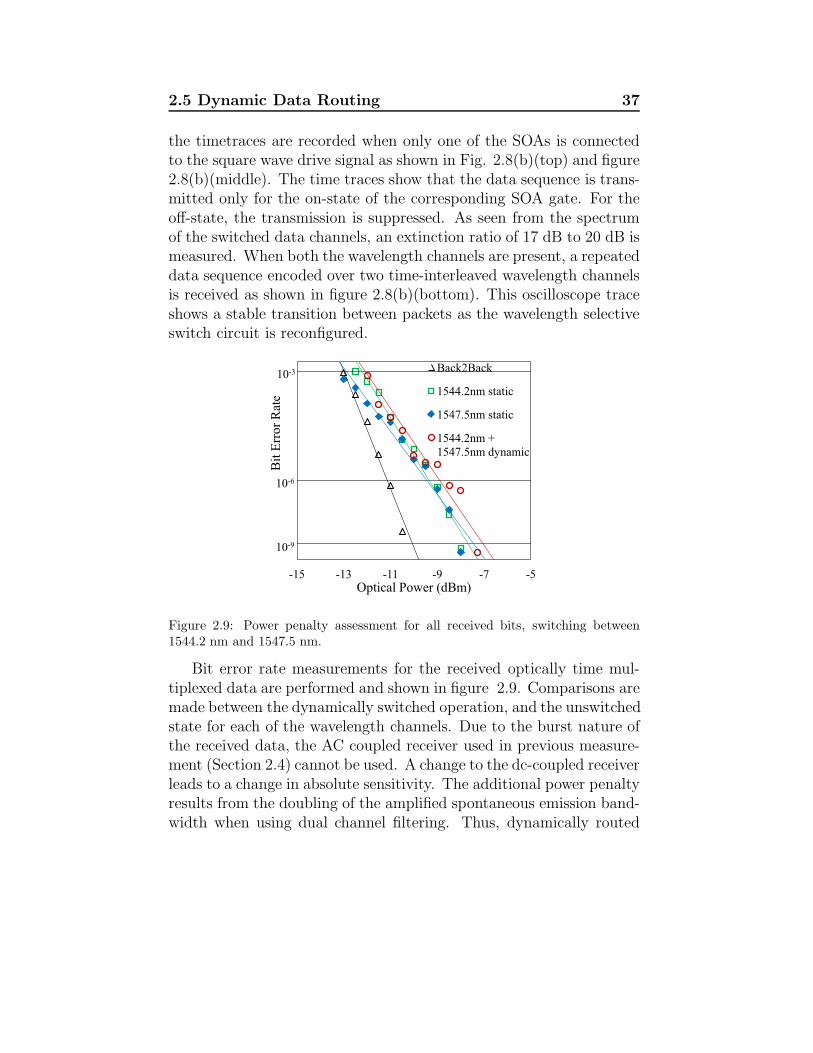
Figure 2.9: Power penalty assessment for all received bits, switching between1544.2 nm and 1547.5 nm.
Bit error rate measurements for the received optically time mul-tiplexed data are performed and shown in figure 2.9. Comparisons aremade between the dynamically switched operation, and the unswitchedstate for each of the wavelength channels. Due to the burst nature ofthe received data, the AC coupled receiver used in previous measure-ment (Section 2.4) cannot be used. A change to the dc-coupled receiverleads to a change in absolute sensitivity. The additional power penaltyresults from the doubling of the amplified spontaneous emission band-width when using dual channel filtering. Thus, dynamically routed
38 Gated Arrayed Waveguide Grating
time multiplexed data exhibits a power penalty of 3.0 dB, which isonly marginally higher than the values measured for static operation.Two data points even imply a negative power penalty can be achieved,but the logarithmic trend lines indicate that this is within measure-ment accuracy. This dynamic power is measured for all bits receivedat the output with a very short 2 ns guard time signifying a very highlink utilization.
2.5.2 Remote optical label-based routing
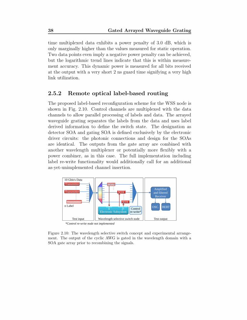
The proposed label-based reconfiguration scheme for the WSS node isshown in Fig. 2.10. Control channels are multiplexed with the datachannels to allow parallel processing of labels and data. The arrayedwaveguide grating separates the labels from the data and uses labelderived information to define the switch state. The designation asdetector SOA and gating SOA is defined exclusively by the electronicdriver circuits: the photonic connections and design for the SOAsare identical. The outputs from the gate array are combined withanother wavelength multiplexer or potentially more flexibly with apower combiner, as in this case. The full implementation includinglabel re-write functionality would additionally call for an additionalas-yet-unimplemented channel insertion.
SOA
Electronic Subsystem
SOA
SOA
n 2n Control re-write*
Transmitter
.....
...
10 Gbit/s Data
Transmitter
Transmittern Label
Test input Wavelength selective switch node Test output
...
.....
Amplified and filtered Receiver
OSC. BERT
*Control re-write node not implemented
Figure 2.10: The wavelength selective switch concept and experimental arrange-ment. The output of the cyclic AWG is gated in the wavelength domain with aSOA gate array prior to recombining the signals.
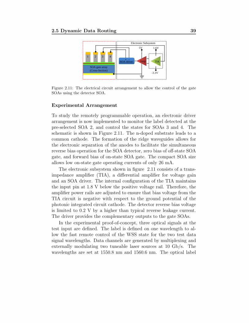
2.5 Dynamic Data Routing 39
TIAAmp
5V
-3.3V
+ -SOA driver
1.6V
1 2 3 4
SOA gate array(Cross-Section)
Electronic Subsystem
Figure 2.11: The electrical circuit arrangement to allow the control of the gateSOAs using the detector SOA.
Experimental Arrangement
To study the remotely programmable operation, an electronic driverarrangement is now implemented to monitor the label detected at thepre-selected SOA 2, and control the states for SOAs 3 and 4. Theschematic is shown in Figure 2.11. The n-doped substrate leads to acommon cathode. The formation of the ridge waveguides allows forthe electronic separation of the anodes to facilitate the simultaneousreverse bias operation for the SOA detector, zero bias of off-state SOAgate, and forward bias of on-state SOA gate. The compact SOA sizeallows low on-state gate operating currents of only 26 mA.
The electronic subsystem shown in figure 2.11 consists of a trans-impedance amplifier (TIA), a differential amplifier for voltage gainand an SOA driver. The internal configuration of the TIA maintainsthe input pin at 1.8 V below the positive voltage rail. Therefore, theamplifier power rails are adjusted to ensure that bias voltage from theTIA circuit is negative with respect to the ground potential of thephotonic integrated circuit cathode. The detector reverse bias voltageis limited to 0.2 V by a higher than typical reverse leakage current.The driver provides the complementary outputs to the gate SOAs.
In the experimental proof-of-concept, three optical signals at thetest input are defined. The label is defined on one wavelength to al-low the fast remote control of the WSS state for the two test datasignal wavelengths. Data channels are generated by multiplexing andexternally modulating two tuneable laser sources at 10 Gb/s. Thewavelengths are set at 1550.8 nm and 1560.6 nm. The optical label
40 Gated Arrayed Waveguide Grating
is generated at the third wavelength of 1556 nm and is multiplexedwith the data channels before being input to the circuit. Polarizationcontrol is implemented on the input side of the WSS. The presenceof the optical label signal enables the routing of wavelength channel1550.8 nm and the absence leads to the routing of the wavelengthchannel 1560.6 nm. For the dynamic routing studies, the pattern trig-ger signal from the bit error rate tester is used to create a square wavemodulation for the control channel. This is defined to be thirty-twotimes longer than the selected 29-1 pattern length and is synchronizedto the pseudo random bit sequence. The choice of sequence allows fora relatively short label length - the state toggles between high and loweach 819.2ns - while remaining sufficiently long to permit gated errormeasurements under dynamic label routing conditions.
In this demonstration, the WSS is operated in 4×1 configuration.The AWG within the WSS chip directs each of the data channel andthe control channel to their corresponding SOAs. In this study, SOA2is designated as a label detector and reversed biased at 0.2 V. Forthe label input optical power of -0.5dBm (in-fibre), 150 µA peak topeak photocurrent is generated. A trans-impedance gain of 4000 andsubsequent voltage amplification generates a 3 Volts peak to peaksignal to trigger the SOA driver. The driver generates complementarysquare-wave signals with peak-to-peak voltage of 2.5 V. Signal delaysof 95 ns are observed between the detected label and generated driversignals resulting primarily from the choice of amplifiers and drivers(the driver alone incurs 60 ns delay), but this can be radically reducedas no electronic or fibre delays are required in principle.
Dynamic label-based switching
The dynamically reconfigured operation is assessed by means of biterror rate measurements and through the monitoring of time-resolvedcircuit outputs. Fig. 2.12(a)(i) through (iii) show the electrical signalsmeasured within the electronic subsystem. Fig. 2.12(a)(i) shows theoptical control signal at the input of the WSS. The signal is outputfrom detector SOA2 and leads to the complementary signals for gateSOAs 3 and 4. For this toggling between switch states, the traces (iv)
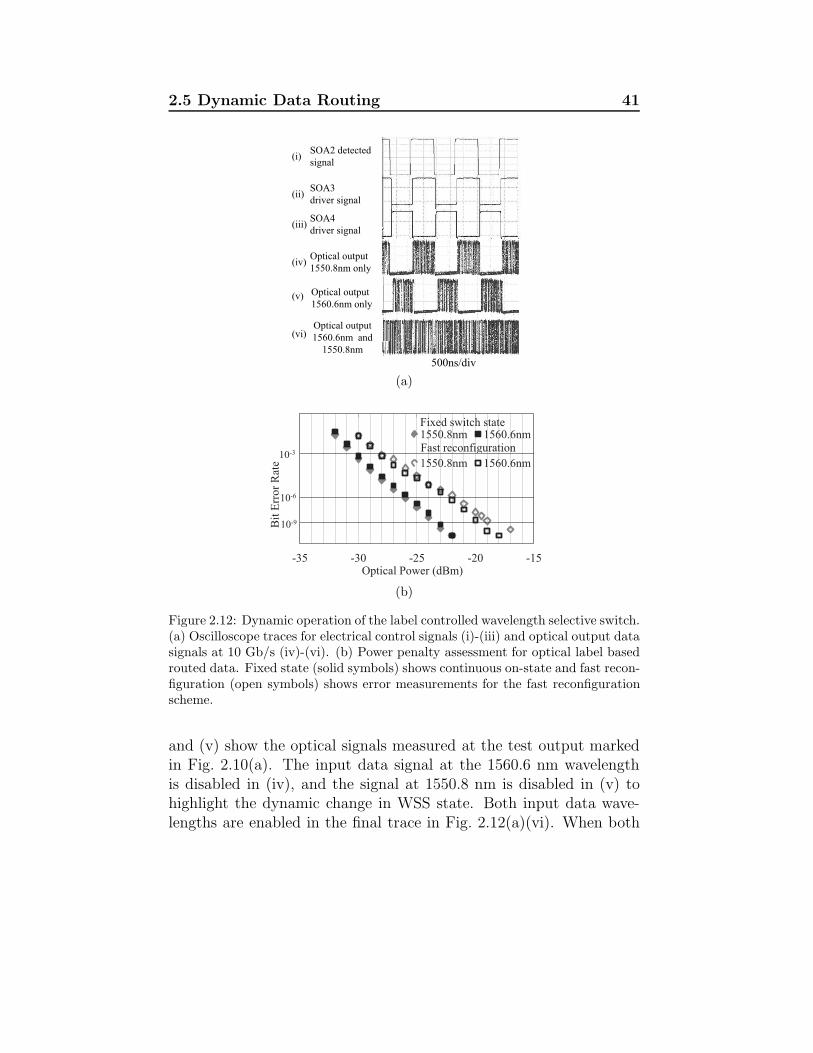
2.5 Dynamic Data Routing 41
Optical output
1550.8nm only
Optical output
1560.6nm only
Optical output
1560.6nm and
1550.8nm
500ns/div
SOA2 detected
signal
SOA3
driver signal
SOA4
driver signal
(i)
(ii)
(iii)
(iv)
(v)
(vi)
(a)
-35 -30 -25 -20 -15
1550.8nm 1560.6nm
1550.8nm 1560.6nm10-3
10-6
10-9Bit
Err
or
Rat
e
Optical Power (dBm)
Fixed switch state
Fast reconfiguration
(b)
Figure 2.12: Dynamic operation of the label controlled wavelength selective switch.(a) Oscilloscope traces for electrical control signals (i)-(iii) and optical output datasignals at 10 Gb/s (iv)-(vi). (b) Power penalty assessment for optical label basedrouted data. Fixed state (solid symbols) shows continuous on-state and fast recon-figuration (open symbols) shows error measurements for the fast reconfigurationscheme.
and (v) show the optical signals measured at the test output markedin Fig. 2.10(a). The input data signal at the 1560.6 nm wavelengthis disabled in (iv), and the signal at 1550.8 nm is disabled in (v) tohighlight the dynamic change in WSS state. Both input data wave-lengths are enabled in the final trace in Fig. 2.12(a)(vi). When both
42 Gated Arrayed Waveguide Grating
the channels co-exist, the output of the chip consists of dynamicallyrouted time multiplexed wavelength channels.
The received data at the output is amplified, filtered using a dualband filter and assessed in terms of the bit error rate. The BER dataare shown in Fig. 2.12(b). Comparisons are made between the fixedswitch states for both high and low level of optical control signal andfor fast switch reconfiguration. The bit error rate measurements forthe fixed switch state data is taken firstly in the presence and secondlyin the absence of the control signal i.e. enabling only one channel topass through the device for each set of measurements. The BER datashown in the solid symbols are near identical, indicating no significantpenalty due to the presence of the label signal. For the case of thetoggled optical control signal, separate gated error measurements wereperformed with a 632.2 ns measurement window for time intervalscorresponding to the two label states. An additional power penaltyof 4 dB is measured for each of the dynamically switched wavelengthchannel. The power penalty measured is believed to be degraded bythe crosstalk at the receiver between the two correlated data channels.The imperfect unwanted signal extinction can be improved by eitherincreasing the SOA length, or by driving the SOA gates with a negativeoff-state signal to increase the off-state extinction.
2.6 Discussion
Low gate operating powers (26 mA current and 1.34 V voltage) pergate leads to picoJoule per bit optoelectronic switching energy (1.16pJ/bit) for the 3λ × 10 Gb/s data rates demonstrated. This is verypromising for scalability of the architecture to larger port counts. Thecascaded MMI stages for the SOA gate array do however add 3.5log2NdB to the on-chip loss for N connections. Loss-free operation does how-ever remain a possibility through increased gain in the SOAs gates.This would also enable an improved extinction ratio and thereby re-duce problematic crosstalk [126] at an expense of increased total powerconsumption. This is necessary for higher connectivity and highernumbers of channels. A space switch preceding the WSS will addi-
2.7 Summary 43
tionally enable more sophisticated system level routing. Such a 4×4space and wavelength cross-connect is studied in detail in Chapter 3.
2.7 Summary
The first characterization of the SOA gated cyclic AWG is presentedfor multi-wavelength dynamic switch operation. Multiband operationis shown for 3λ ×10 Gb/s channels with 0.2-1.0 dB power penalty.Nanosecond timescale reconfiguration is achieved with less than 2 nsswitching time. A power penalty of 3.0 dB is measured for nanosecondtimescale dynamic wavelength routing. Self-routing is proposed usinga monolithic approach to combine optical label reading and signalgating within a wavelength selective switch. This allows the potentialreduction of hardware complexity and energy loss for a fast reconfig-urable circuit. Proof of principle dynamic switching is performed andgives 4 dB power penalty with nanosecond time-scale reconfiguration.With a compact chip area of less than 5 mm2, simplified digital control,fabrication-tolerant and scalable design proposed is a highly promisingapproach to hardware-efficient wavelength-agile networking.

3Integrated 4×4 Space andWavelength Cross-connect
In this chapter1, the first monolithically integrated 4×4 cross-connectis designed, fabricated2 and characterized for static and dynamic rout-ing operation. Multi-path routing is demonstrated for both co- andcounter-propagating 10 Gb/s data channels. The first demonstrationof simultaneous routing of three 40 Gb/s input signals is presentedwith low power penalty for multiple routed channels. Dynamic rout-ing is demonstrated using multiple hops with nanosecond timescaleswitching speed.
3.1 Introduction
Prior to this work, fast integrated wavelength selective optical cross-connects (WS-OXC) have been primarily limited to 2×2 configura-tions (Ref. Table 1.2 in Chapter 1). The key limitation in scalingthe demonstrated integrated WS-OXC to N×N arrangements is thelarge device size associated with MZI switches. Moreover, control com-plexity associated with MZI switches and thermal issues due to largeinput power per active path [19] has limited the data routing demon-
1Based on the results published in [127–131]2in JePPIX multi-project wafer (MPW) process [49]
46 Integrated 4×4 Space and Wavelength Cross-connect
strated so far to a single 40 Gb/s channel (Table 1.2). However, tobe practically useful for system implementation, there is a demand formulti-port colorless, direction-less and contention-less design. Color-less signifies that any wavelength can be routed from any input to anyselected output. Direction-less means that the OXC should be ableto handle data in both directions. Contention issues can be managedto some extent by fanning out to more gates than connections and byusing multiple output receivers [15].
In this chapter, a combination of space switching and wavelengthswitching is exploited to achieve a robust scalable integrated solutionto handle multiple wavelength channels and provide nanosecond re-configurability. A 4×4 monolithically integrated cross-connect basedon four shuffled 1×4 space switches with four wavelength selectiveswitches has been designed and fabricated. SOAs are used for gat-ing as well as for on-chip loss compensation. The cross-connect isdesigned to achieve high connectivity by simultaneously routing anywavelength from a given input port to any given output port. Thearchitecture and design considerations are discussed in Section 3.2.The routing performance of the cross-connect is experimentally evalu-ated and detailed device characterization is presented in Section 3.3.Simultaneous routing of multiple 10 Gb/s data channels through theintegrated 4×4 cross-connect is presented in Section 3.4. Data in-tegrity for co- and counter propagating WDM data is evaluated interm of the measured power penalty for each channel. Nanoseconddynamic re-configurability is also demonstrated for the full circuit us-ing multiple hops. Lastly, line rate scalability is shown with multi-path co-propagating 3×40 Gb/s data channels in Section 3.5. Dataintegrity is evaluated in terms of measured power penalty for eachchannel.
3.2 4×4 Space and Wavelength Cross-connect
3.2.1 Architecture
The 4-input 4-output space and wavelength cross-connect architectureis shown schematically in Fig. 3.1. A fan-out is implemented using
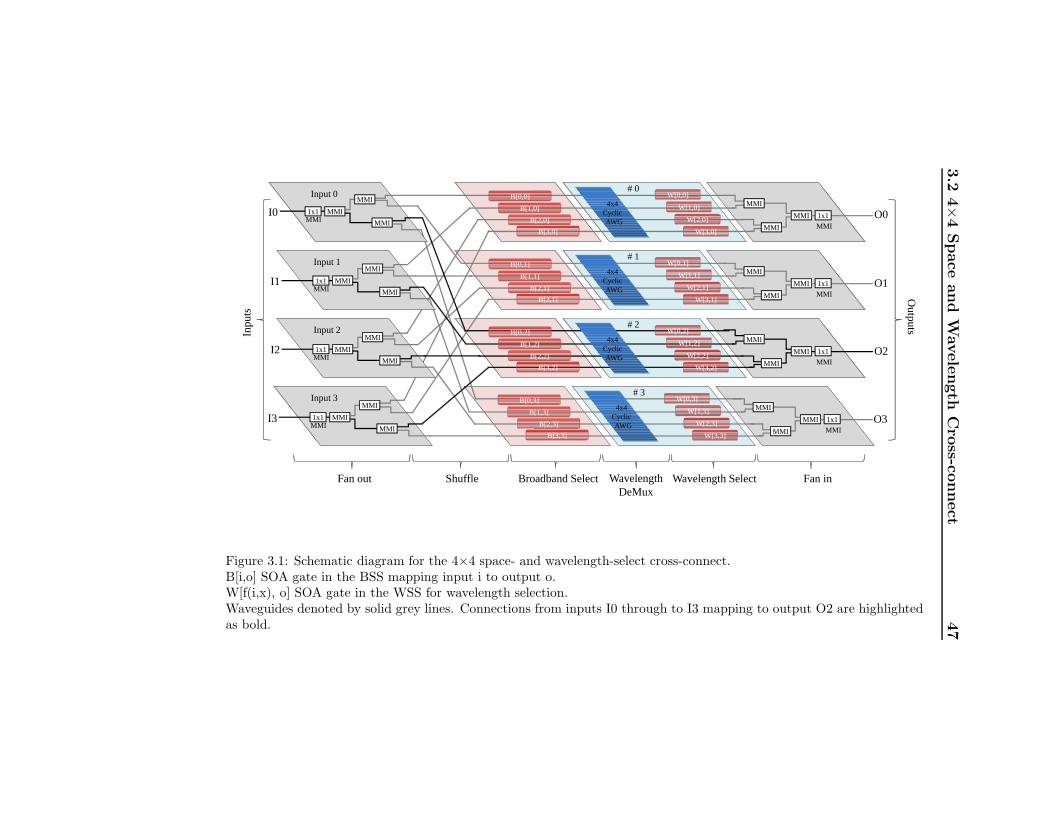
3.2
4×4Spaceand
Wavelength
Cro
ss-connect
47
Inpu
ts
Outputs
W[3,0]
W[2,0]
W[1,0]
W[0,0]
MMI
MMI
MMI
MMI
1x1
MMI
MMI
MMI
MMI
1x1
MMI
MMI
MMI
MMI
1x1
W[3,3]
W[2,3]
4x4CyclicAWG
W[1,3]
W[0,3]
MMI
MMI
MMI
MMI
1x1
4x4CyclicAWG
W[3,1]
W[2,1]
W[1,1]
W[0,1]
W[3,2]
W[2,2]
W[1,2]
W[0,2]
B[2,0]
B[0,0]
B[1,0]
B[3,0]
B[2,3]
B[0,3]
B[1,3]
B[3,3]
B[0,1]
B[2,1]
B[1,1]
B[3,1]
B[2,2]
B[0,2]
B[1,2]
B[3,2]
O3
O0
O1
O2
# 0
# 1
# 2
# 3
4x4CyclicAWG
4x4CyclicAWG
I3
I0
Input 3
MMI1x1MMI MMI
MMI
Input 0
MMI1x1MMI MMI
MMI
I1
Input 1
MMI1x1MMI MMI
MMI
I2
Input 2
MMI1x1MMI MMI
MMI
Fan out Wavelength DeMux
Shuffle Broadband Select Wavelength Select Fan in
Figure 3.1: Schematic diagram for the 4×4 space- and wavelength-select cross-connect.B[i,o] SOA gate in the BSS mapping input i to output o.W[f(i,x), o] SOA gate in the WSS for wavelength selection.Waveguides denoted by solid grey lines. Connections from inputs I0 through to I3 mapping to output O2 are highlightedas bold.
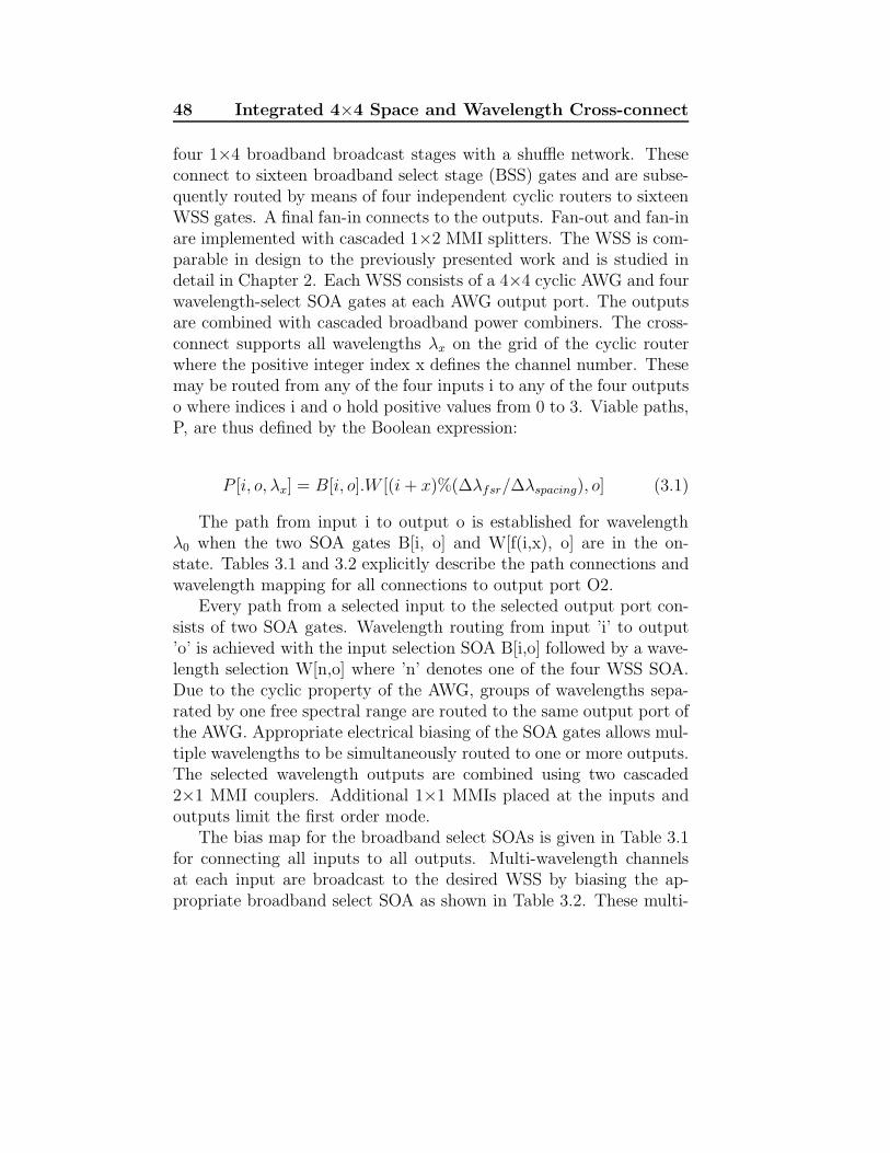
48 Integrated 4×4 Space and Wavelength Cross-connect
four 1×4 broadband broadcast stages with a shuffle network. Theseconnect to sixteen broadband select stage (BSS) gates and are subse-quently routed by means of four independent cyclic routers to sixteenWSS gates. A final fan-in connects to the outputs. Fan-out and fan-inare implemented with cascaded 1×2 MMI splitters. The WSS is com-parable in design to the previously presented work and is studied indetail in Chapter 2. Each WSS consists of a 4×4 cyclic AWG and fourwavelength-select SOA gates at each AWG output port. The outputsare combined with cascaded broadband power combiners. The cross-connect supports all wavelengths λx on the grid of the cyclic routerwhere the positive integer index x defines the channel number. Thesemay be routed from any of the four inputs i to any of the four outputso where indices i and o hold positive values from 0 to 3. Viable paths,P, are thus defined by the Boolean expression:
P [i, o, λx] = B[i, o].W [(i+ x)%(∆λfsr/∆λspacing), o] (3.1)
The path from input i to output o is established for wavelengthλ0 when the two SOA gates B[i, o] and W[f(i,x), o] are in the on-state. Tables 3.1 and 3.2 explicitly describe the path connections andwavelength mapping for all connections to output port O2.
Every path from a selected input to the selected output port con-sists of two SOA gates. Wavelength routing from input ’i’ to output’o’ is achieved with the input selection SOA B[i,o] followed by a wave-length selection W[n,o] where ’n’ denotes one of the four WSS SOA.Due to the cyclic property of the AWG, groups of wavelengths sepa-rated by one free spectral range are routed to the same output port ofthe AWG. Appropriate electrical biasing of the SOA gates allows mul-tiple wavelengths to be simultaneously routed to one or more outputs.The selected wavelength outputs are combined using two cascaded2×1 MMI couplers. Additional 1×1 MMIs placed at the inputs andoutputs limit the first order mode.
The bias map for the broadband select SOAs is given in Table 3.1for connecting all inputs to all outputs. Multi-wavelength channelsat each input are broadcast to the desired WSS by biasing the ap-propriate broadband select SOA as shown in Table 3.2. These multi-
3.2 4×4 Space and Wavelength Cross-connect 49
Table 3.1: Broadband select stage (BSS) configuration. On-stateswitch for one broadband connection
InputOutput o
0 1 2 3
0 B[0,0] B[0,1] B[0,2] B[0,3]
1 B[1,0] B[1,1] B[1,2] B[1,3]
2 B[2,0] B[2,1] B[2,2] B[2,3]
3 B[3,0] B[3,1] B[3,2] B[3,3]
Table 3.2: Wavelength select stage (WSS) configuration map to out-put 2. On-state switches for one wavelength specific connection.
Output O2 O2 O2 O2
Input BSS W[0,2] W[1,2] W[2,2] W[3,2]
I0 B[0,2] λ0 λ1 λ2 λ3
I1 B[1,2] λ3 λ0 λ1 λ2
I2 B[2,2] λ2 λ3 λ0 λ1
I3 B[3,2] λ1 λ2 λ3 λ0
wavelength channels are then de-multiplexed by the cyclic AWG. De-pending on the selected input port, the wavelengths are routed todifferent AWG output ports. The four wavelengths/wavebands span-ning one free spectral range, denoted as λ0, λ1, λ2, λ3 are consideredas inputs to each input port. The shuffle network broadcasts multi-wavelength data to the corresponding B[i,o]. These broadband selectSOAs pass or block the WDM data channels from the selected inputport to the following WSS. They have the dual purpose of selectingwavelength multiplexed inputs as well as providing on-chip loss com-pensation for the broadcast operation. The cyclic AWG separates thefour wavelengths into separate AWG output ports depending on theselected input.
50 Integrated 4×4 Space and Wavelength Cross-connect
The detailed wavelength mapping for multi-wavelength channelsfrom all inputs to output 2 is shown in Table 3.2. One or more ofthese wavelengths are finally selected by wavelength select SOAs androuted to the output.
3.2.2 Design
The mask layout of the 4×4 space and wavelength cross-connect isshown in figure 3.2(a). The cross-connect is realized on a JePPIXmulti-project wafer process [49] at COBRA. Similar epitaxy is usedas in the case of the wavelength selective switch discussed in Chap-ter 2. Both deep and shallow etched waveguides are used. The 1×1fundamental-spatial-mode filter is used at the input as well as output.MMIs are defined in deep-etched waveguide with a width and lengthof 6.5 µm and 46.5 µm respectively with 1.7 µm input-output wave-guides. Tapered transition sections between deep-etched and shallowetched circuit elements minimize reflections at the interfaces. Thiscircuit is processed with inductively coupled plasma (ICP) etch to de-fine highly-vertical sidewalls. This is expected to lead to minimumpolarization rotation despite the extensive use of curved waveguidesin the circuit layout [132]. This process run was performed on a full2-inch wafer with the designs repeated in each quarter keeping thesame orientation. Two chips centered at different radial locations onthe wafer are characterized in this chapter. Chip 1 is placed closer tothe periphery while chip 2 lies closer to the wafer center.
The waveguide crossings used in the shuffle network are imple-mented as shallow-etched waveguides to reduce divergence and there-fore signal loss. Switches are implemented as SOA gates. Only twelve30 µm×750 µm active islands are available within the chip area, somultiple SOAs are implemented at each active island in the circuitimplementation. Pairs of 750 µm long BSS SOAs share the centraleight active islands. Four 140 µm long WSS SOAs share each islandat both the top and bottom of the mask layout in Fig. 3.2(b). Toensure adequate separation between the WSS SOAs, the waveguidesare angled across the islands. The longer BSS SOAs are expected toprovide significant gain in addition to the switching function, while
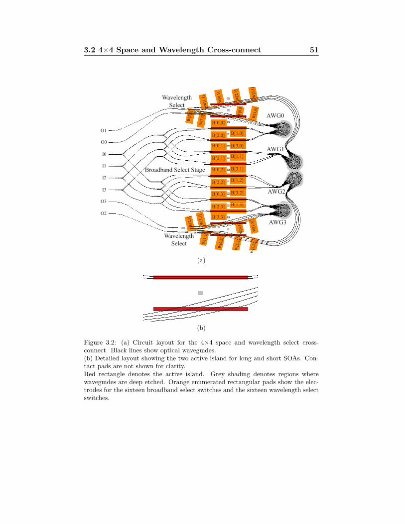
3.2 4×4 Space and Wavelength Cross-connect 51
Wavelength
Select
AWG0B[0,0]
AWG1
O1
O0
I0
B[1,0]B[2,0]
B[3,0]B[0,1]
B[1 1]
Broadband Select Stage
I0
I1
I2
B[1,1]B[2,1]
B[3,1]B[0,2]
B[1,2]B[2 2]
AWG2I3
O3
[ , ]B[2,2]
B[3,2]B[0,3]
B[1,3]B[2,3]
Wavelength
AWG3
O2
[ ]
B[3,3]
Wavelength
Select
(a)
(b)
Figure 3.2: (a) Circuit layout for the 4×4 space and wavelength select cross-connect. Black lines show optical waveguides.(b) Detailed layout showing the two active island for long and short SOAs. Con-tact pads are not shown for clarity.Red rectangle denotes the active island. Grey shading denotes regions wherewaveguides are deep etched. Orange enumerated rectangular pads show the elec-trodes for the sixteen broadband select switches and the sixteen wavelength selectswitches.
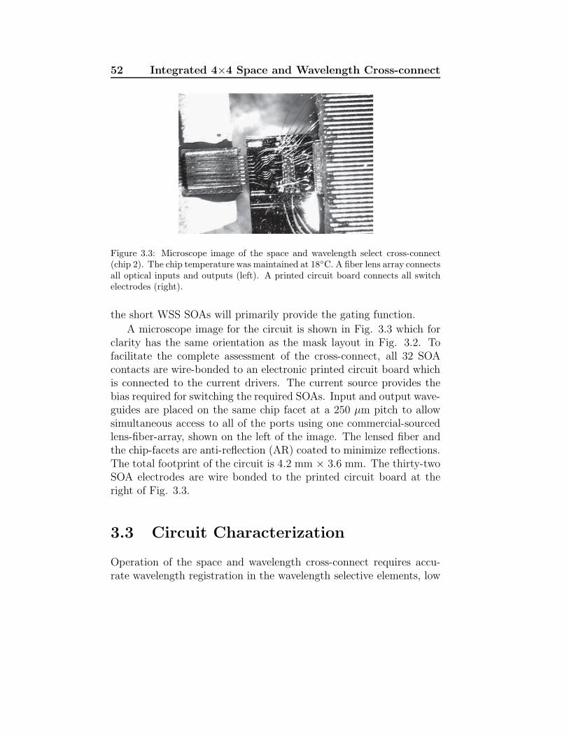
52 Integrated 4×4 Space and Wavelength Cross-connect
Figure 3.3: Microscope image of the space and wavelength select cross-connect(chip 2). The chip temperature was maintained at 18C. A fiber lens array connectsall optical inputs and outputs (left). A printed circuit board connects all switchelectrodes (right).
the short WSS SOAs will primarily provide the gating function.
A microscope image for the circuit is shown in Fig. 3.3 which forclarity has the same orientation as the mask layout in Fig. 3.2. Tofacilitate the complete assessment of the cross-connect, all 32 SOAcontacts are wire-bonded to an electronic printed circuit board whichis connected to the current drivers. The current source provides thebias required for switching the required SOAs. Input and output wave-guides are placed on the same chip facet at a 250 µm pitch to allowsimultaneous access to all of the ports using one commercial-sourcedlens-fiber-array, shown on the left of the image. The lensed fiber andthe chip-facets are anti-reflection (AR) coated to minimize reflections.The total footprint of the circuit is 4.2 mm × 3.6 mm. The thirty-twoSOA electrodes are wire bonded to the printed circuit board at theright of Fig. 3.3.
3.3 Circuit Characterization
Operation of the space and wavelength cross-connect requires accu-rate wavelength registration in the wavelength selective elements, low
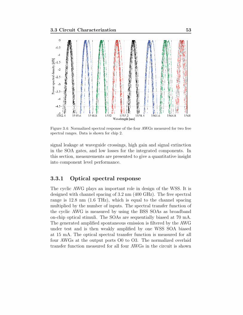
3.3 Circuit Characterization 53
Figure 3.4: Normalized spectral response of the four AWGs measured for two freespectral ranges. Data is shown for chip 2.
signal leakage at waveguide crossings, high gain and signal extinctionin the SOA gates, and low losses for the integrated components. Inthis section, measurements are presented to give a quantitative insightinto component level performance.
3.3.1 Optical spectral response
The cyclic AWG plays an important role in design of the WSS. It isdesigned with channel spacing of 3.2 nm (400 GHz). The free spectralrange is 12.8 nm (1.6 THz), which is equal to the channel spacingmultiplied by the number of inputs. The spectral transfer function ofthe cyclic AWG is measured by using the BSS SOAs as broadbandon-chip optical stimuli. The SOAs are sequentially biased at 70 mA.The generated amplified spontaneous emission is filtered by the AWGunder test and is then weakly amplified by one WSS SOA biasedat 15 mA. The optical spectral transfer function is measured for allfour AWGs at the output ports O0 to O3. The normalized overlaidtransfer function measured for all four AWGs in the circuit is shown
54 Integrated 4×4 Space and Wavelength Cross-connect
in figure 3.4. The measured transfer functions for all the measuredcombinations are assessed in terms of pass-band peak wavelength and3 dB bandwidth. The path to path variability and the range of valuesis quantified in terms of the mean and standard deviation values inTable 3.3. Spectra is additionally plotted for the more uniform chip 2in Fig. 3.4.
A total of 21% and 52% of the possible 43 path combinations aresuccessfully assessed for chips 1 and 2 respectively. A small number ofwaveguide breaks and SOA fails prevent all paths from being estab-lished. The spectral responses for the four AWGs are very similar inshape. The channel spacing and 3 dB pass bandwidth are measured tobe 400 GHz and 180 GHz as intended. There is a discernible mismatchbetween one of the AWGs and the remaining three for Chip 2 as seenfrom the figure 3.4. There is also a higher level of variability for Chip1, as summarized quantitatively in Table 3.3. This non-uniformitycan result from the process variation at the center and edge of the2-inch InP wafer. Discrepancy in the width of the arrayed waveguidesacross the chip due to possible wafer inhomogeneities, as well as thethickness of the overlaying layers can influence the effective refractiveindex and the optical mode. This can influence the wavelength shiftin the AWGs. The mean channel spacing of 400 GHz is measured witha standard deviation of 74.8 GHz and 25.9 GHz for chip 1 and chip 2respectively.
3.3.2 Optical loss
Passive component losses for the MMI devices and the AWG router arepredicted using the commercial software FimmProp [133] and AgilentAdvanced Design System with in-house extensions respectively. Losspredictions for the components indicate small excess losses per com-ponent of order 0.5 dB. Mode propagation simulations performed fortwo orthogonally defined 2 µm wide shallow-etched waveguides giveloss estimations of order 0.2 dB per crossing.
Experimental estimations of loss have also been performed and arealso summarized in Table 3.3. Crossing loss may be estimated to afirst order by noting that the number of waveguide crossings between

3.3 Circuit Characterization 55
Table 3.3: Component and circuit performance
Components (Numbers) Mean values (Standard Deviations σ)
Arrayed waveguide gratings
Spectral channel spacing
Design target 400 GHz
Chip 1 (27 passbands measured) 400 (σ=75 GHz)
Chip 2 (66 passbands measured) 400 (σ=26 GHz)
Spectral pass bandwidth
Design target 180 GHz
Chip 1 (27 paths measured) 183 (σ=38 GHz)
Chip 2 (66 paths measured) 180 (σ=10 GHz)
AWG peak transmission (1 per path)
ADS simulation with extensions1 4.0 dB loss
Fiber-chip coupling loss (2 per path)
Chip 1 and 2 7.5 dB loss per fiber
Waveguide loss
Test chips give 3.5 dB/cm 2.8 dB to 3.5 dB total
Multi-mode interference devices
1×2 MMI splitter (4 per path)
Fimmprop optical mode solver 3.5 dB per splitter
1×1 MMI mode filter (2 per path)
Fimmprop optical mode solver 0.5 dB per splitter
Waveguide crossing
Loss (0 to 6 per path)
Fimmprop optical mode solver 0.20 dB per crossing
Chip 1 and 2 0.25 dB per crossing (σ=0.48)
Circuit Paths2
Transparency (zero gain SOAs)
Sum of passive component losses 21.8 dB to 23.7 dB loss
Chip 2 (36 paths measured) 23.7 dB (σ=2.0 dB) loss
On-state gain (high current SOAs)
Predicted from SOA gain and loss 1.2 dB gain to 0.7 dB loss
Chip 1 (12 paths measured)3 9.4 dB loss (σ=5.8 dB)
Chip 1 (best case path measured)3 2.8 dB loss
Chip 2 (12 paths measured)3 4.1 dB loss
1 with in-house optical solver extensions implemented by Dr. X.J.M. Leijtens.2 Net chip loss is specified without fiber to chip coupling losses. i.e. 15 dB totalfiber-chip coupling losses have been subtracted.3 Measured with SOAs operating current density of 5 kA/cm2.
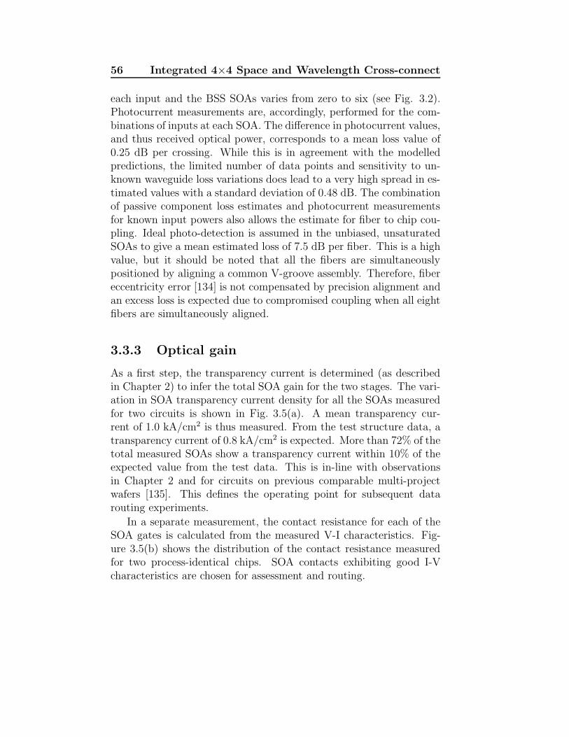
56 Integrated 4×4 Space and Wavelength Cross-connect
each input and the BSS SOAs varies from zero to six (see Fig. 3.2).Photocurrent measurements are, accordingly, performed for the com-binations of inputs at each SOA. The difference in photocurrent values,and thus received optical power, corresponds to a mean loss value of0.25 dB per crossing. While this is in agreement with the modelledpredictions, the limited number of data points and sensitivity to un-known waveguide loss variations does lead to a very high spread in es-timated values with a standard deviation of 0.48 dB. The combinationof passive component loss estimates and photocurrent measurementsfor known input powers also allows the estimate for fiber to chip cou-pling. Ideal photo-detection is assumed in the unbiased, unsaturatedSOAs to give a mean estimated loss of 7.5 dB per fiber. This is a highvalue, but it should be noted that all the fibers are simultaneouslypositioned by aligning a common V-groove assembly. Therefore, fibereccentricity error [134] is not compensated by precision alignment andan excess loss is expected due to compromised coupling when all eightfibers are simultaneously aligned.
3.3.3 Optical gain
As a first step, the transparency current is determined (as describedin Chapter 2) to infer the total SOA gain for the two stages. The vari-ation in SOA transparency current density for all the SOAs measuredfor two circuits is shown in Fig. 3.5(a). A mean transparency cur-rent of 1.0 kA/cm2 is thus measured. From the test structure data, atransparency current of 0.8 kA/cm2 is expected. More than 72% of thetotal measured SOAs show a transparency current within 10% of theexpected value from the test data. This is in-line with observationsin Chapter 2 and for circuits on previous comparable multi-projectwafers [135]. This defines the operating point for subsequent datarouting experiments.
In a separate measurement, the contact resistance for each of theSOA gates is calculated from the measured V-I characteristics. Fig-ure 3.5(b) shows the distribution of the contact resistance measuredfor two process-identical chips. SOA contacts exhibiting good I-Vcharacteristics are chosen for assessment and routing.
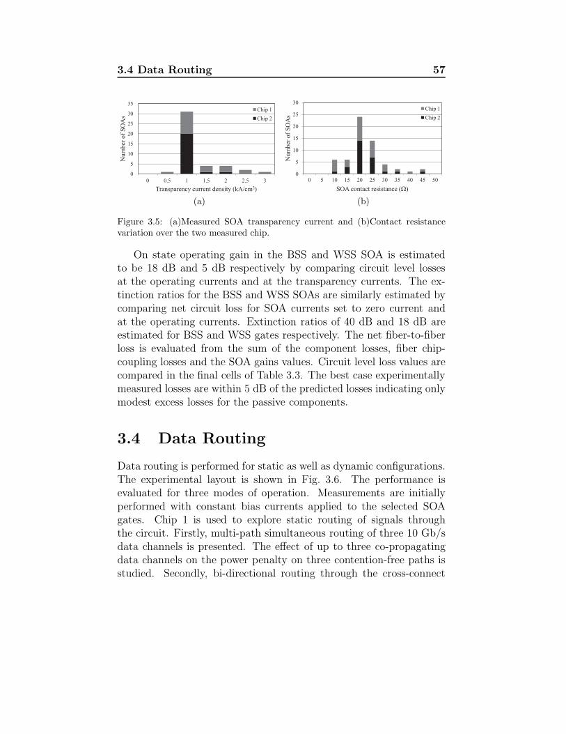
3.4 Data Routing 57
Nu
mb
er o
f S
OA
s
0
5
10
15
20
25
30
35
0 0.5 1 1.5 2 2.5 3
Nu
mb
er o
f S
OA
s
Transparency current density (kA/cm2)
Chip 1
Chip 2
(a)
0
5
10
15
20
25
30
0 5 10 15 20 25 30 35 40 45 50
Nu
mb
er o
f S
OA
s
SOA contact resistance ( )
Chip 1
Chip 2
0 0.5 1 1.5 2 2.5 3
Chip 1
Chip 2
(b)
Figure 3.5: (a)Measured SOA transparency current and (b)Contact resistancevariation over the two measured chip.
On state operating gain in the BSS and WSS SOA is estimatedto be 18 dB and 5 dB respectively by comparing circuit level lossesat the operating currents and at the transparency currents. The ex-tinction ratios for the BSS and WSS SOAs are similarly estimated bycomparing net circuit loss for SOA currents set to zero current andat the operating currents. Extinction ratios of 40 dB and 18 dB areestimated for BSS and WSS gates respectively. The net fiber-to-fiberloss is evaluated from the sum of the component losses, fiber chip-coupling losses and the SOA gains values. Circuit level loss values arecompared in the final cells of Table 3.3. The best case experimentallymeasured losses are within 5 dB of the predicted losses indicating onlymodest excess losses for the passive components.
3.4 Data Routing
Data routing is performed for static as well as dynamic configurations.The experimental layout is shown in Fig. 3.6. The performance isevaluated for three modes of operation. Measurements are initiallyperformed with constant bias currents applied to the selected SOAgates. Chip 1 is used to explore static routing of signals throughthe circuit. Firstly, multi-path simultaneous routing of three 10 Gb/sdata channels is presented. The effect of up to three co-propagatingdata channels on the power penalty on three contention-free paths isstudied. Secondly, bi-directional routing through the cross-connect
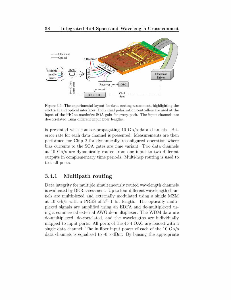
58 Integrated 4×4 Space and Wavelength Cross-connect
Electrical
Optical To Receiver
Multiple
tunable
lasers
10
/ 4
0 G
b/s
PR
BS
Dat
aAMP
Mu
x
MZM
BPG/BERT
Electrical
Driver
Receiver
Clock
Sync
De-
Mu
x
OSC
Figure 3.6: The experimental layout for data routing assessment, highlighting theelectrical and optical interfaces. Individual polarization controllers are used at theinput of the PIC to maximize SOA gain for every path. The input channels arede-correlated using different input fiber lengths.
is presented with counter-propagating 10 Gb/s data channels. Bit-error rate for each data channel is presented. Measurements are thenperformed for Chip 2 for dynamically reconfigured operation wherebias currents to the SOA gates are time variant. Two data channelsat 10 Gb/s are dynamically routed from one input to two differentoutputs in complementary time periods. Multi-hop routing is used totest all ports.
3.4.1 Multipath routing
Data integrity for multiple simultaneously routed wavelength channelsis evaluated by BER assessment. Up to four different wavelength chan-nels are multiplexed and externally modulated using a single MZMat 10 Gb/s with a PRBS of 231-1 bit length. The optically multi-plexed signals are amplified using an EDFA and de-multiplexed us-ing a commercial external AWG de-multiplexer. The WDM data arede-multiplexed, de-correlated, and the wavelengths are individuallymapped to input ports. All ports of the 4×4 OXC are loaded with asingle data channel. The in-fiber input power of each of the 10 Gb/sdata channels is equalized to -0.5 dBm. By biasing the appropriate
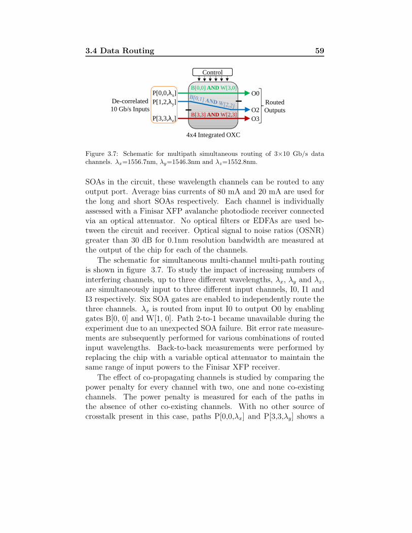
3.4 Data Routing 59
De-correlated 10 Gb/s Inputs
B[0,0] AND W[3,0]P[0,0,λx]P[1,2,λy]
P[3,3,λz]
O0
O2O3
Routed Outputs
B[3,3] AND W[2,3]
Control
4x4 Integrated OXC
Figure 3.7: Schematic for multipath simultaneous routing of 3×10 Gb/s datachannels. λx=1556.7nm, λy=1546.3nm and λz=1552.8nm.
SOAs in the circuit, these wavelength channels can be routed to anyoutput port. Average bias currents of 80 mA and 20 mA are used forthe long and short SOAs respectively. Each channel is individuallyassessed with a Finisar XFP avalanche photodiode receiver connectedvia an optical attenuator. No optical filters or EDFAs are used be-tween the circuit and receiver. Optical signal to noise ratios (OSNR)greater than 30 dB for 0.1nm resolution bandwidth are measured atthe output of the chip for each of the channels.
The schematic for simultaneous multi-channel multi-path routingis shown in figure 3.7. To study the impact of increasing numbers ofinterfering channels, up to three different wavelengths, λx, λy and λz,are simultaneously input to three different input channels, I0, I1 andI3 respectively. Six SOA gates are enabled to independently route thethree channels. λx is routed from input I0 to output O0 by enablinggates B[0, 0] and W[1, 0]. Path 2-to-1 became unavailable during theexperiment due to an unexpected SOA failure. Bit error rate measure-ments are subsequently performed for various combinations of routedinput wavelengths. Back-to-back measurements were performed byreplacing the chip with a variable optical attenuator to maintain thesame range of input powers to the Finisar XFP receiver.
The effect of co-propagating channels is studied by comparing thepower penalty for every channel with two, one and none co-existingchannels. The power penalty is measured for each of the paths inthe absence of other co-existing channels. With no other source ofcrosstalk present in this case, paths P[0,0,λx] and P[3,3,λy] shows a
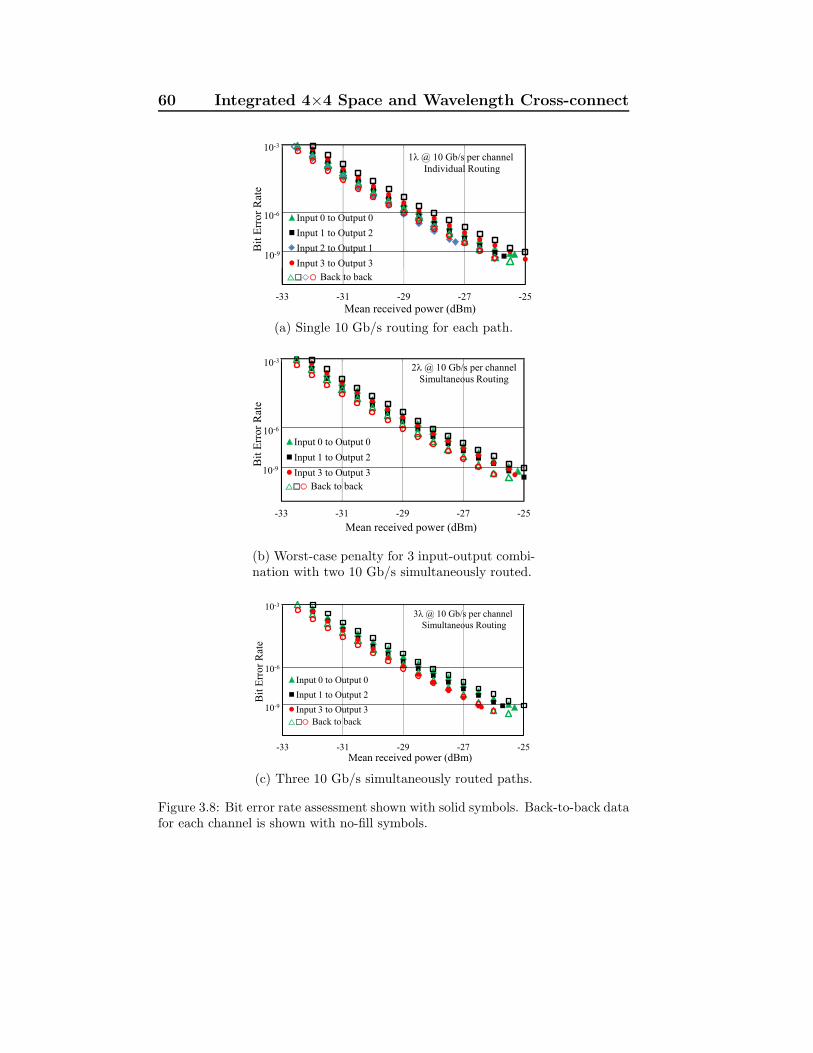
60 Integrated 4×4 Space and Wavelength Cross-connect
-33 -31 -29 -27 -25
Bit
Err
or
Rat
e
Mean received power (dBm)
1 @ 10 Gb/s per channel
Individual Routing
Input 0 to Output 0
Input 1 to Output 2
Input 2 to Output 1
Input 3 to Output 310-9
10-6
10-3
Input 3 to Output 3Input 3 to Output 3
Back to back
(a) Single 10 Gb/s routing for each path.
-33 -31 -29 -27 -25
Bit
Err
or
Rat
e
Mean received power (dBm)
2 @ 10 Gb/s per channel
Simultaneous Routing
Input 0 to Output 0
Input 1 to Output 2
Input 3 to Output 310-9
10-6
10-3
Input 3 to Output 3Input 3 to Output 3
Back to back
(b) Worst-case penalty for 3 input-output combi-nation with two 10 Gb/s simultaneously routed.
-33 -31 -29 -27 -25
Bit
Err
or
Rat
e
Mean received power (dBm)
Input 0 to Output 0
Input 1 to Output 2
Input 3 to Output 3
10-6
10-9
10-3
3 @ 10 Gb/s per channel
Simultaneous Routing
Back to back
(c) Three 10 Gb/s simultaneously routed paths.
Figure 3.8: Bit error rate assessment shown with solid symbols. Back-to-back datafor each channel is shown with no-fill symbols.
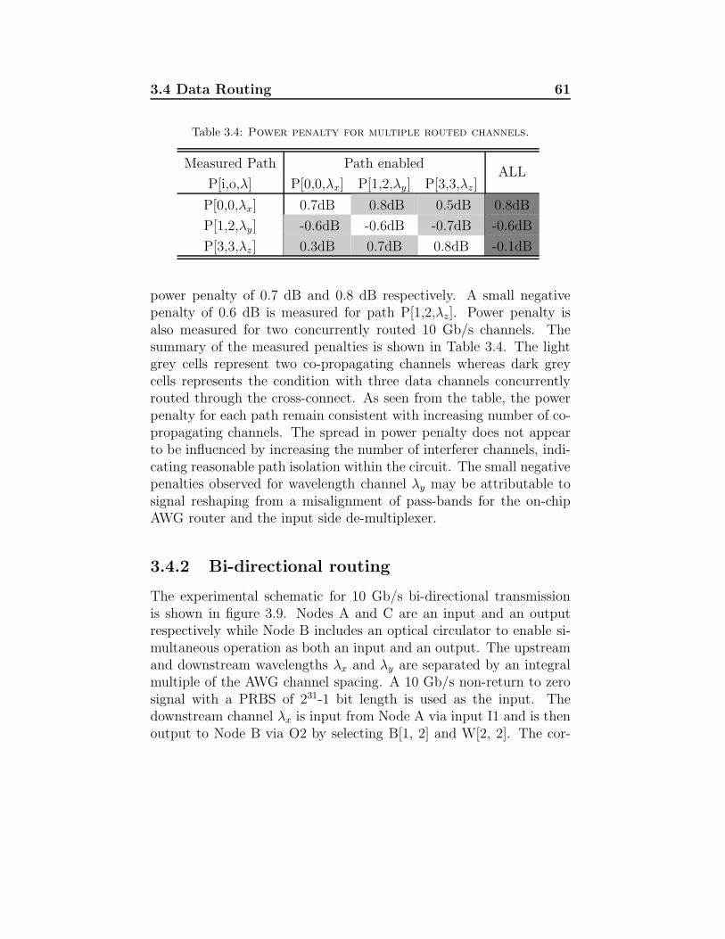
3.4 Data Routing 61
Table 3.4: Power penalty for multiple routed channels.
Measured Path Path enabledALL
P[i,o,λ] P[0,0,λx] P[1,2,λy] P[3,3,λz]
P[0,0,λx] 0.7dB 0.8dB 0.5dB 0.8dB
P[1,2,λy] -0.6dB -0.6dB -0.7dB -0.6dB
P[3,3,λz] 0.3dB 0.7dB 0.8dB -0.1dB
power penalty of 0.7 dB and 0.8 dB respectively. A small negativepenalty of 0.6 dB is measured for path P[1,2,λz]. Power penalty isalso measured for two concurrently routed 10 Gb/s channels. Thesummary of the measured penalties is shown in Table 3.4. The lightgrey cells represent two co-propagating channels whereas dark greycells represents the condition with three data channels concurrentlyrouted through the cross-connect. As seen from the table, the powerpenalty for each path remain consistent with increasing number of co-propagating channels. The spread in power penalty does not appearto be influenced by increasing the number of interferer channels, indi-cating reasonable path isolation within the circuit. The small negativepenalties observed for wavelength channel λy may be attributable tosignal reshaping from a misalignment of pass-bands for the on-chipAWG router and the input side de-multiplexer.
3.4.2 Bi-directional routing
The experimental schematic for 10 Gb/s bi-directional transmissionis shown in figure 3.9. Nodes A and C are an input and an outputrespectively while Node B includes an optical circulator to enable si-multaneous operation as both an input and an output. The upstreamand downstream wavelengths λx and λy are separated by an integralmultiple of the AWG channel spacing. A 10 Gb/s non-return to zerosignal with a PRBS of 231-1 bit length is used as the input. Thedownstream channel λx is input from Node A via input I1 and is thenoutput to Node B via O2 by selecting B[1, 2] and W[2, 2]. The cor-
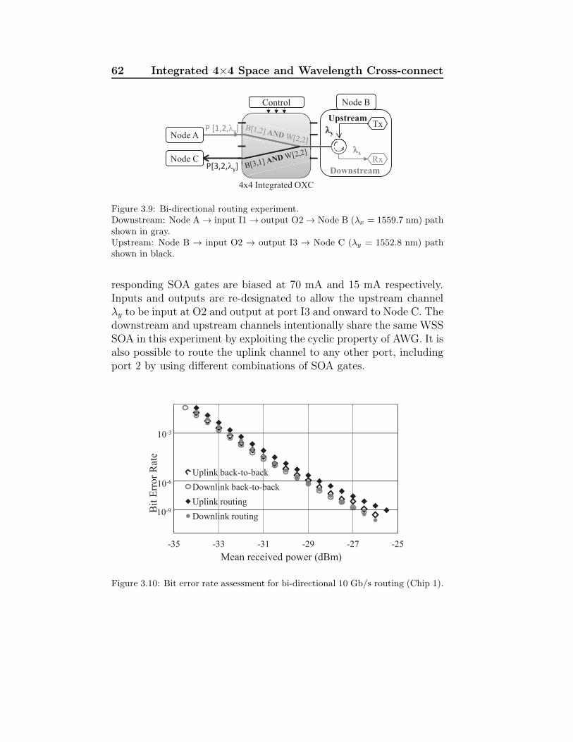
62 Integrated 4×4 Space and Wavelength Cross-connectO3
P[3,2, y]
Node A
Node C
y
x
Upstream
Downstream
Node B
Tx
Rx
4x4 Integrated OXC
P [1,2, x]
Control
Figure 3.9: Bi-directional routing experiment.Downstream: Node A → input I1 → output O2 → Node B (λx = 1559.7 nm) pathshown in gray.Upstream: Node B → input O2 → output I3 → Node C (λy = 1552.8 nm) pathshown in black.
responding SOA gates are biased at 70 mA and 15 mA respectively.Inputs and outputs are re-designated to allow the upstream channelλy to be input at O2 and output at port I3 and onward to Node C. Thedownstream and upstream channels intentionally share the same WSSSOA in this experiment by exploiting the cyclic property of AWG. It isalso possible to route the uplink channel to any other port, includingport 2 by using different combinations of SOA gates.
-35 -33 -31 -29 -27 -25
Uplink back-to-back
Downlink back-to-back
Uplink routing
Downlink routing10-9
10-6
10-3
Bit
Err
or
Rat
e
Mean received power (dBm)
Figure 3.10: Bit error rate assessment for bi-directional 10 Gb/s routing (Chip 1).
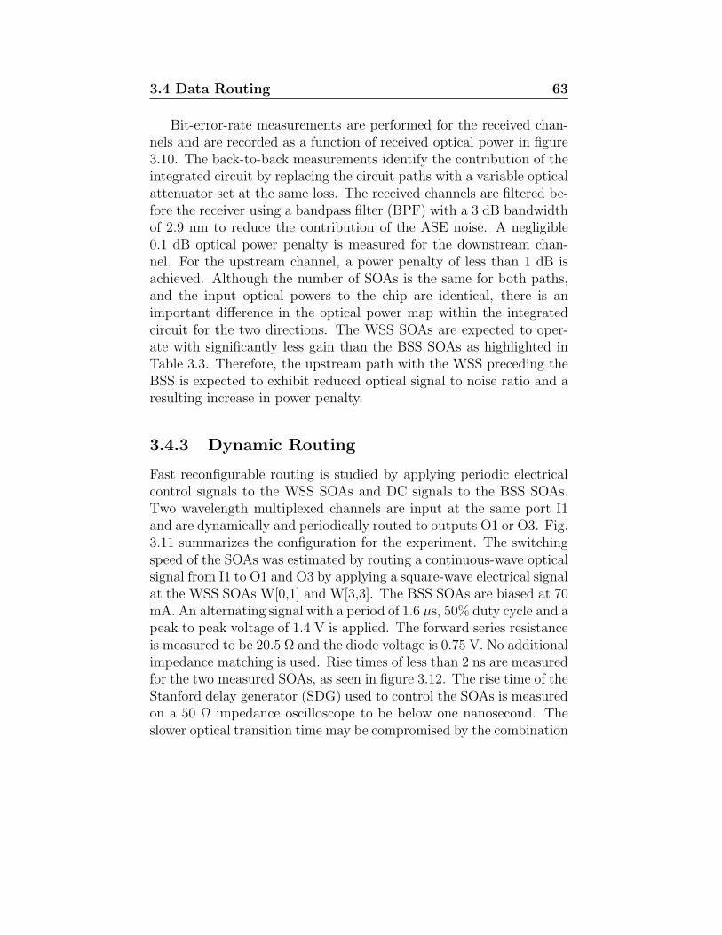
3.4 Data Routing 63
Bit-error-rate measurements are performed for the received chan-nels and are recorded as a function of received optical power in figure3.10. The back-to-back measurements identify the contribution of theintegrated circuit by replacing the circuit paths with a variable opticalattenuator set at the same loss. The received channels are filtered be-fore the receiver using a bandpass filter (BPF) with a 3 dB bandwidthof 2.9 nm to reduce the contribution of the ASE noise. A negligible0.1 dB optical power penalty is measured for the downstream chan-nel. For the upstream channel, a power penalty of less than 1 dB isachieved. Although the number of SOAs is the same for both paths,and the input optical powers to the chip are identical, there is animportant difference in the optical power map within the integratedcircuit for the two directions. The WSS SOAs are expected to oper-ate with significantly less gain than the BSS SOAs as highlighted inTable 3.3. Therefore, the upstream path with the WSS preceding theBSS is expected to exhibit reduced optical signal to noise ratio and aresulting increase in power penalty.
3.4.3 Dynamic Routing
Fast reconfigurable routing is studied by applying periodic electricalcontrol signals to the WSS SOAs and DC signals to the BSS SOAs.Two wavelength multiplexed channels are input at the same port I1and are dynamically and periodically routed to outputs O1 or O3. Fig.3.11 summarizes the configuration for the experiment. The switchingspeed of the SOAs was estimated by routing a continuous-wave opticalsignal from I1 to O1 and O3 by applying a square-wave electrical signalat the WSS SOAs W[0,1] and W[3,3]. The BSS SOAs are biased at 70mA. An alternating signal with a period of 1.6 µs, 50% duty cycle and apeak to peak voltage of 1.4 V is applied. The forward series resistanceis measured to be 20.5 Ω and the diode voltage is 0.75 V. No additionalimpedance matching is used. Rise times of less than 2 ns are measuredfor the two measured SOAs, as seen in figure 3.12. The rise time of theStanford delay generator (SDG) used to control the SOAs is measuredon a 50 Ω impedance oscilloscope to be below one nanosecond. Theslower optical transition time may be compromised by the combination
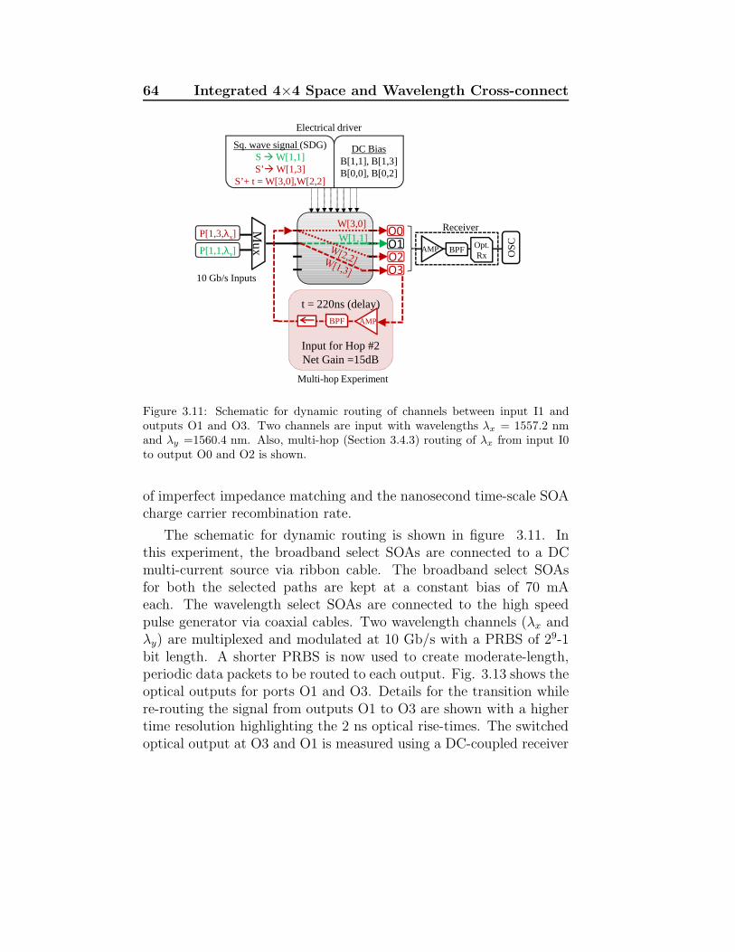
64 Integrated 4×4 Space and Wavelength Cross-connect
t = 220ns (delay)
Input for Hop #2Net Gain =15dB
BPF AMP
BPF Opt. Rx O
SC
AMP
ReceiverP[1,3,λx]
DC BiasB[1,1], B[1,3]B[0,0], B[0,2]
W[1,1]
10 Gb/s Inputs
Mux
W[3,0]
P[1,1,λy]
Sq. wave signal (SDG) S W[1,1] S’ W[1,3]
S’+ t = W[3,0],W[2,2]
Electrical driver
Multi-hop Experiment
Figure 3.11: Schematic for dynamic routing of channels between input I1 andoutputs O1 and O3. Two channels are input with wavelengths λx = 1557.2 nmand λy =1560.4 nm. Also, multi-hop (Section 3.4.3) routing of λx from input I0to output O0 and O2 is shown.
of imperfect impedance matching and the nanosecond time-scale SOAcharge carrier recombination rate.
The schematic for dynamic routing is shown in figure 3.11. Inthis experiment, the broadband select SOAs are connected to a DCmulti-current source via ribbon cable. The broadband select SOAsfor both the selected paths are kept at a constant bias of 70 mAeach. The wavelength select SOAs are connected to the high speedpulse generator via coaxial cables. Two wavelength channels (λx andλy) are multiplexed and modulated at 10 Gb/s with a PRBS of 29-1bit length. A shorter PRBS is now used to create moderate-length,periodic data packets to be routed to each output. Fig. 3.13 shows theoptical outputs for ports O1 and O3. Details for the transition whilere-routing the signal from outputs O1 to O3 are shown with a highertime resolution highlighting the 2 ns optical rise-times. The switchedoptical output at O3 and O1 is measured using a DC-coupled receiver
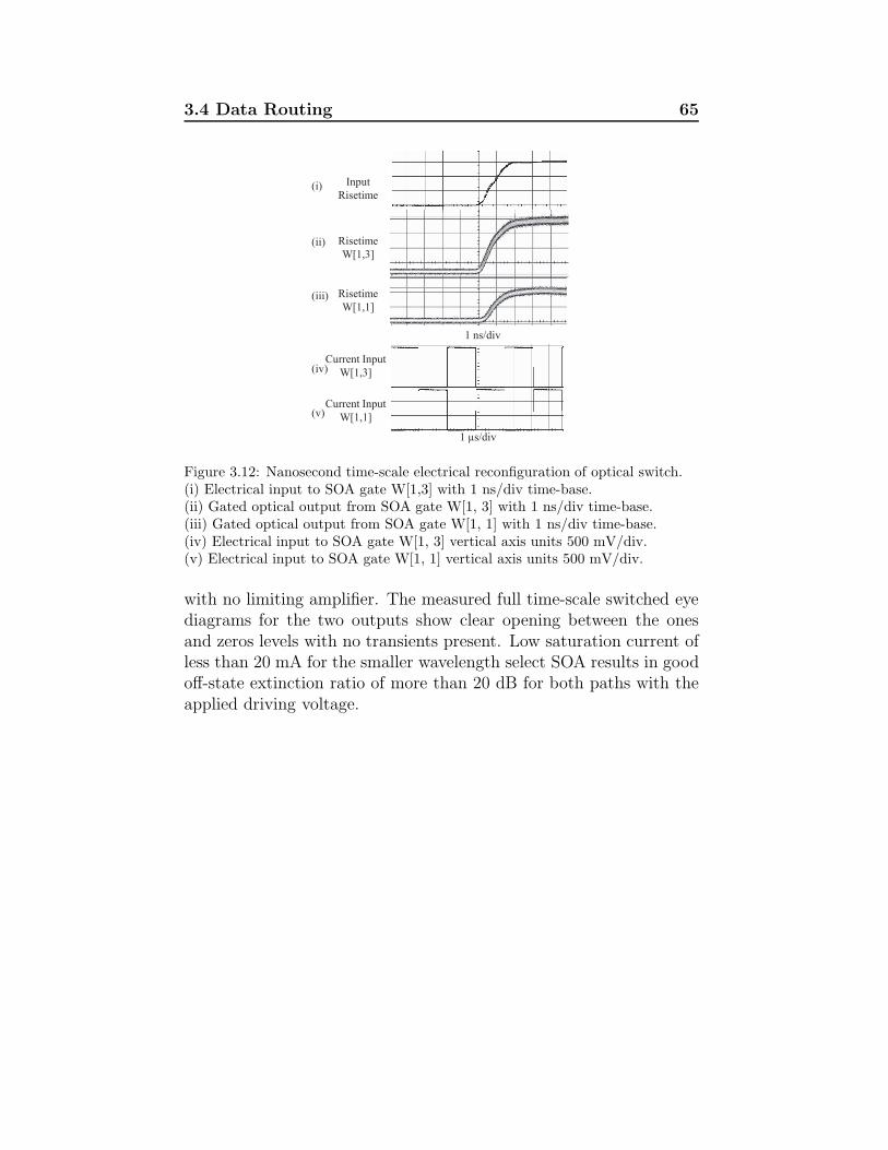
3.4 Data Routing 65
Input
Risetime
Current Input
W[1,3]
Current Input
W[1,1]
1 ns/div
Risetime
W[1,3]
Risetime
W[1,1]
1 µs/div
(iv)
(v)
(i)
(ii)
(iii)
Figure 3.12: Nanosecond time-scale electrical reconfiguration of optical switch.(i) Electrical input to SOA gate W[1,3] with 1 ns/div time-base.(ii) Gated optical output from SOA gate W[1, 3] with 1 ns/div time-base.(iii) Gated optical output from SOA gate W[1, 1] with 1 ns/div time-base.(iv) Electrical input to SOA gate W[1, 3] vertical axis units 500 mV/div.(v) Electrical input to SOA gate W[1, 1] vertical axis units 500 mV/div.
with no limiting amplifier. The measured full time-scale switched eyediagrams for the two outputs show clear opening between the onesand zeros levels with no transients present. Low saturation current ofless than 20 mA for the smaller wavelength select SOA results in goodoff-state extinction ratio of more than 20 dB for both paths with theapplied driving voltage.
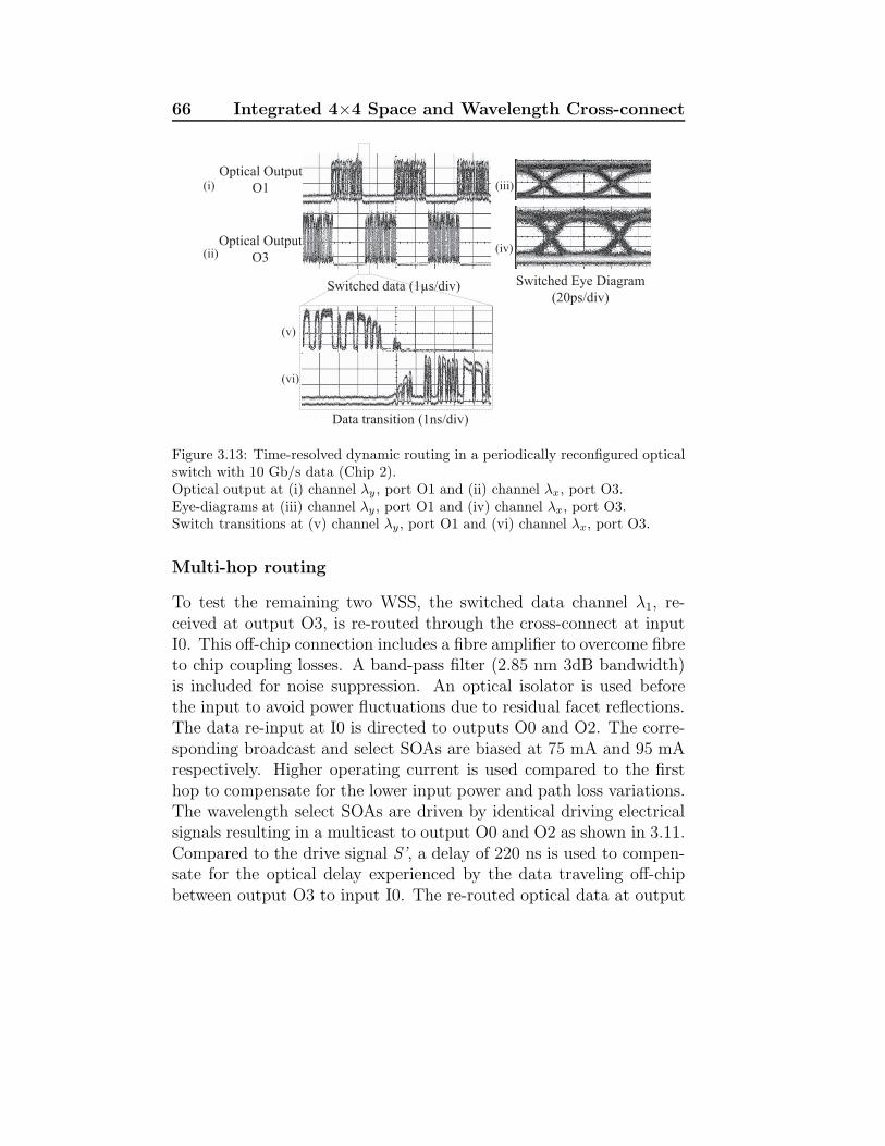
66 Integrated 4×4 Space and Wavelength Cross-connect
Optical Output
O1
Data transition (1ns/div)
Optical Output
O3
Switched Eye Diagram
(20ps/div)
(i)
(ii)
(iii)
(iv)
(v)
(vi)
Switched data (1µs/div)
Figure 3.13: Time-resolved dynamic routing in a periodically reconfigured opticalswitch with 10 Gb/s data (Chip 2).Optical output at (i) channel λy , port O1 and (ii) channel λx, port O3.Eye-diagrams at (iii) channel λy , port O1 and (iv) channel λx, port O3.Switch transitions at (v) channel λy, port O1 and (vi) channel λx, port O3.
Multi-hop routing
To test the remaining two WSS, the switched data channel λ1, re-ceived at output O3, is re-routed through the cross-connect at inputI0. This off-chip connection includes a fibre amplifier to overcome fibreto chip coupling losses. A band-pass filter (2.85 nm 3dB bandwidth)is included for noise suppression. An optical isolator is used beforethe input to avoid power fluctuations due to residual facet reflections.The data re-input at I0 is directed to outputs O0 and O2. The corre-sponding broadcast and select SOAs are biased at 75 mA and 95 mArespectively. Higher operating current is used compared to the firsthop to compensate for the lower input power and path loss variations.The wavelength select SOAs are driven by identical driving electricalsignals resulting in a multicast to output O0 and O2 as shown in 3.11.Compared to the drive signal S’, a delay of 220 ns is used to compen-sate for the optical delay experienced by the data traveling off-chipbetween output O3 to input I0. The re-routed optical data at output
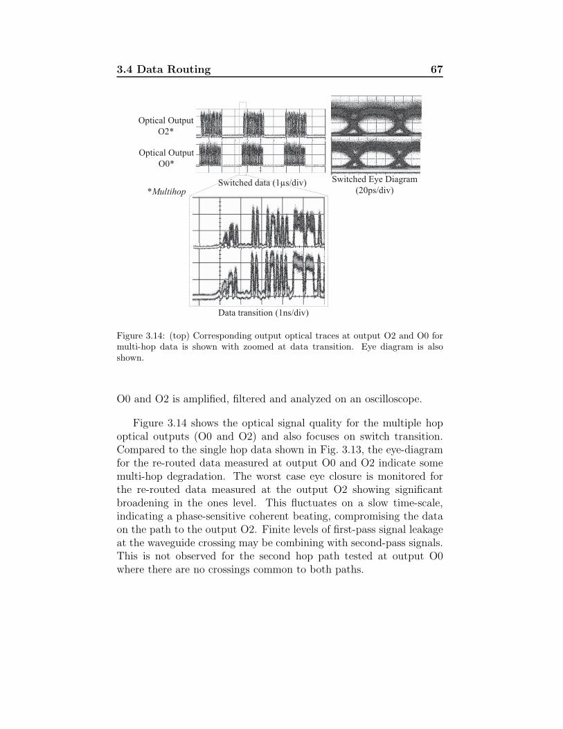
3.4 Data Routing 67
Optical Output
O2*
Optical Output
O0*
Switched Eye Diagram
(20ps/div)
Data transition (1ns/div)
*MultihopSwitched data (1µs/div)
Figure 3.14: (top) Corresponding output optical traces at output O2 and O0 formulti-hop data is shown with zoomed at data transition. Eye diagram is alsoshown.
O0 and O2 is amplified, filtered and analyzed on an oscilloscope.
Figure 3.14 shows the optical signal quality for the multiple hopoptical outputs (O0 and O2) and also focuses on switch transition.Compared to the single hop data shown in Fig. 3.13, the eye-diagramfor the re-routed data measured at output O0 and O2 indicate somemulti-hop degradation. The worst case eye closure is monitored forthe re-routed data measured at the output O2 showing significantbroadening in the ones level. This fluctuates on a slow time-scale,indicating a phase-sensitive coherent beating, compromising the dataon the path to the output O2. Finite levels of first-pass signal leakageat the waveguide crossing may be combining with second-pass signals.This is not observed for the second hop path tested at output O0where there are no crossings common to both paths.
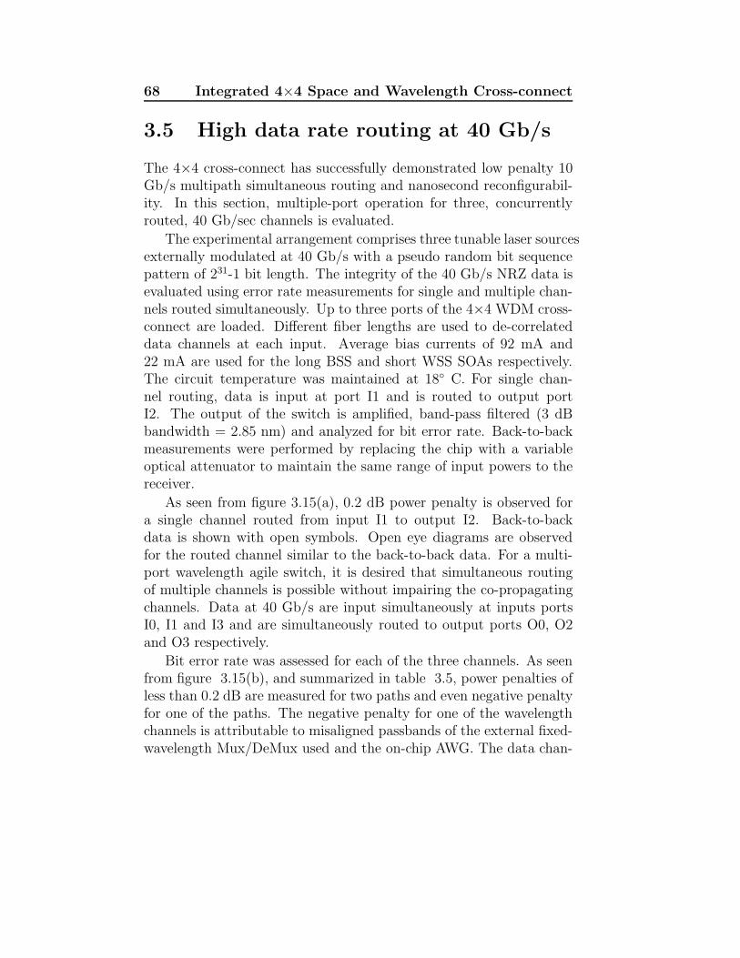
68 Integrated 4×4 Space and Wavelength Cross-connect
3.5 High data rate routing at 40 Gb/s
The 4×4 cross-connect has successfully demonstrated low penalty 10Gb/s multipath simultaneous routing and nanosecond reconfigurabil-ity. In this section, multiple-port operation for three, concurrentlyrouted, 40 Gb/sec channels is evaluated.
The experimental arrangement comprises three tunable laser sourcesexternally modulated at 40 Gb/s with a pseudo random bit sequencepattern of 231-1 bit length. The integrity of the 40 Gb/s NRZ data isevaluated using error rate measurements for single and multiple chan-nels routed simultaneously. Up to three ports of the 4×4 WDM cross-connect are loaded. Different fiber lengths are used to de-correlateddata channels at each input. Average bias currents of 92 mA and22 mA are used for the long BSS and short WSS SOAs respectively.The circuit temperature was maintained at 18 C. For single chan-nel routing, data is input at port I1 and is routed to output portI2. The output of the switch is amplified, band-pass filtered (3 dBbandwidth = 2.85 nm) and analyzed for bit error rate. Back-to-backmeasurements were performed by replacing the chip with a variableoptical attenuator to maintain the same range of input powers to thereceiver.
As seen from figure 3.15(a), 0.2 dB power penalty is observed fora single channel routed from input I1 to output I2. Back-to-backdata is shown with open symbols. Open eye diagrams are observedfor the routed channel similar to the back-to-back data. For a multi-port wavelength agile switch, it is desired that simultaneous routingof multiple channels is possible without impairing the co-propagatingchannels. Data at 40 Gb/s are input simultaneously at inputs portsI0, I1 and I3 and are simultaneously routed to output ports O0, O2and O3 respectively.
Bit error rate was assessed for each of the three channels. As seenfrom figure 3.15(b), and summarized in table 3.5, power penalties ofless than 0.2 dB are measured for two paths and even negative penaltyfor one of the paths. The negative penalty for one of the wavelengthchannels is attributable to misaligned passbands of the external fixed-wavelength Mux/DeMux used and the on-chip AWG. The data chan-
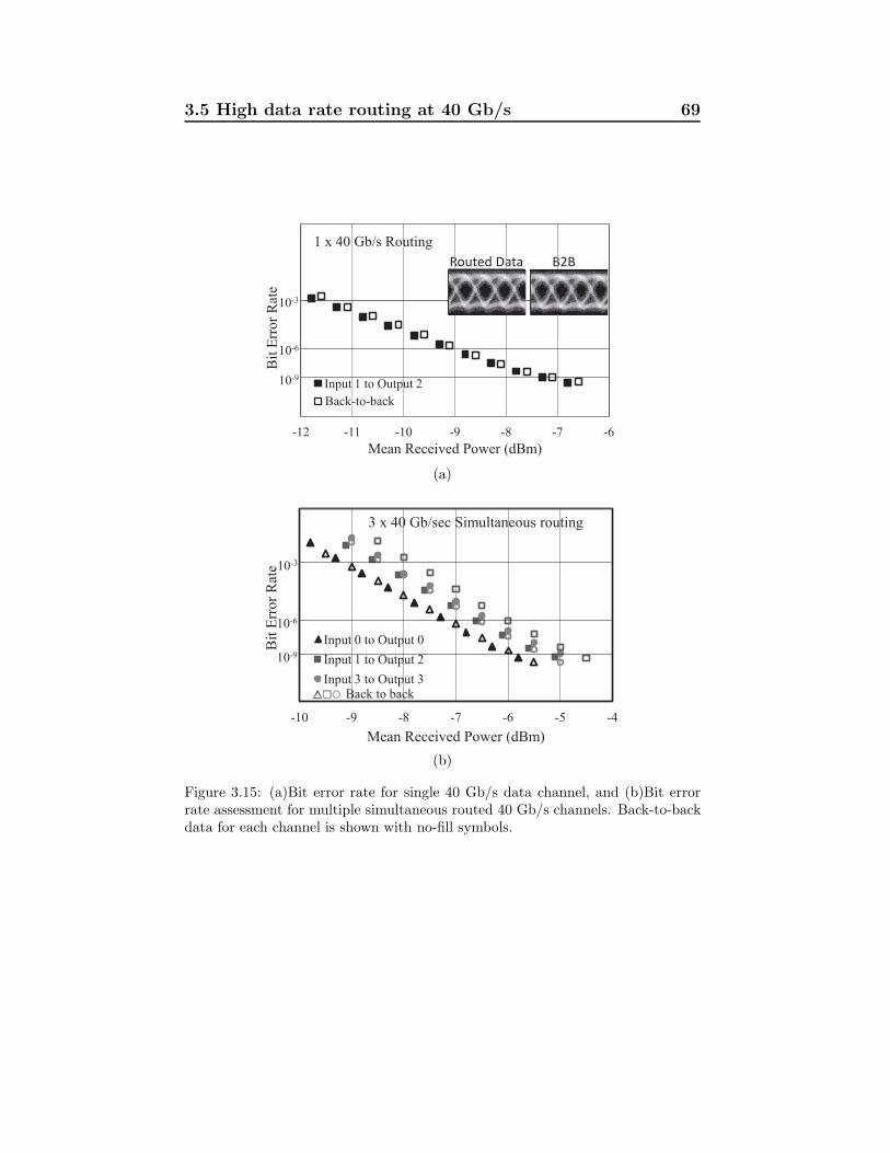
3.5 High data rate routing at 40 Gb/s 69
Back-to-back
B2B Routed Data
-12 -11 -10 -9 -8 -7 -6
Bit
Err
or
Rat
e
Mean Received Power (dBm)
1 x 40 Gb/s Routing
Input 1 to Output 210-9
10-6
10-3
(a)
-10 -9 -8 -7 -6 -5 -4
Bit
Err
or
Rat
e
Mean Received Power (dBm)
3 x 40 Gb/sec Simultaneous routing
Input 0 to Output 0
Input 1 to Output 2
Input 3 to Output 3
10-9
10-6
10-3
Back to back
(b)
Figure 3.15: (a)Bit error rate for single 40 Gb/s data channel, and (b)Bit errorrate assessment for multiple simultaneous routed 40 Gb/s channels. Back-to-backdata for each channel is shown with no-fill symbols.
70 Integrated 4×4 Space and Wavelength Cross-connect
nels are aligned to the on-chip AWG. This results in slight spectralmisalignment at the Mux/DeMux for each wavelength. Hence, theobserved difference in the back-to-back measurements. Comparingmulti-input operation with the single input operation, no additionalpenalty for simultaneous multichannel operation is observed demon-strating the absence of signal impairment due to crosstalk. Opticalsignal to noise ratios greater than 36 dB for 0.1 nm resolution band-width are measured at the output of the chip for each of the threechannels. This is highly promising for future high data rate applica-tions.
Table 3.5: Summary of routing condition.
Input Output Wavelength SOA Bias (mA) Power
Port Port (nm) BSS WSS Penalty (dB)
0 0 1556.75 115 25 0.1
1 2 1546.3 90 24.7 -0.6
3 3 1543.2 70 16 0.2
3.6 Discussion
The first 4×4 space and wavelength select cross-connect has beendemonstrated to provide low penalty multipath routing with nanosec-ond timescale switching speed. The combination of a broadband fan-out, broadband fan-in and a n×n router is implemented with twostage gating. While this integrated circuit does not represent thesame level of architectural complexity as the discrete and partly popu-lated demonstrators listed in Table 1.3, this does represent the highestlevel of integration for current multi-project-wafer integration plat-form technology. The WS-OXC architecture is scalable to large port-counts keeping the number of SOA gates per path constant. Based onthis design, the number of SOAs required is 2×N2 for a N×N cross-connect i.e. 512 SOAs and 2048 SOAs for a 16×16 and 32×32 cross-connect respectively. To compensate for the splitting losses, longer
3.7 Summary 71
SOAs would be required. The minimum average gain required perSOA stage to compensate for the splitting losses in an N×N configu-ration is given by 3.5*log2N dB. For N=64, a gain of 21 dB per SOAstage will be required.
For the 3 × 40 Gb/s static routing, the total optoelectronic switch-ing energy is in the range of 2.9 to 14.5 pJ/bit assuming the best andthe worst bias conditions for all paths. The channel capacity is mainlydependent on the spectral bandwidth of the optical data path. Themean 1.0 dB passband for the AWG is 0.9 nm (110 GHz) allowing thebit rate to be increased further. However, complex integration andcontrol protocols are needed for contention-less operation. As seenfrom Table 3.2, owing to the chip size restrictions in the current de-sign, it provides limited independent control over wavelength selectionto cater four wavelengths per input port. This can be avoided by usingfour 16×16 AWG. The scalability is ultimately limited by the on-chiploss, ASE noise accumulation, the crosstalk resulting from the waveg-uide crossings in the shuffle network, the circuit size and the wiringdensity.
3.7 Summary
An integrated 4×4 space and wavelength cross-connect has been suc-cessfully designed, fabricated and characterized. Static multi-pathrouting operation was demonstrated for both co- and counter-propagating10 Gb/s data channels with power penalty less than 1.0 dB. Forthe first time, simultaneous routing of three 40 Gb/s input signalsis demonstrated with power penalty less than 0.2 dB for multiplerouted channels. Dynamic reconfiguration is shown with less than 2 nsswitching speed using multiple hop routing. This is an important stepfor integrating next-generation, high-connectivity, high-throughput,dynamically-reconfigurable, optical cross-connects.

4Resilient Higher-order
Resonant switch
In this chapter1, a higher-order resonant structure, consisting of cou-pled resonators, is presented as a broadband crossbar-compliant tun-able wavelength selective element. Quantitative study is presented todesign a resilient fifth-order switch on Silicon-on-insulator platform.Fabrication tolerance is presented for moderate length directional cou-plers in terms of coupling coefficient variation and the resulting impacton data integrity. Characterization of a single fifth-order switch ele-ment is presented here. Thermal tuning is presented for both globaland local temperature changes per switch element. Passband integrityis evaluated in terms of power penalty measured for a detuning rangeof more than ± 50 GHz.
4.1 Introduction
High index-contrast SOI integration platforms exploit state-of-the artCMOS foundry processes for reproducibility and sub-nanometer linewidthuniformity [52]. However, due to the high index contrast, even withthis level of linewidth control the implementation of reproducible res-onant structures is very challenging. Wavelength registration errors
1Based on the results published in [80, 136, 137]
74 Resilient Higher-order Resonant switch
between switch elements and signal wavelengths resulting from thisnano-scale feature-size variability within the micro-resonators has ledto component registration errors of order 1 nm [52]. Fabrication tol-erances may be relaxed considerably through the combination of mod-erate size directional couplers of up to 20 µm, moderate 350 GHz freespectral range resonator design and the use of higher-order resonance.
Higher-order resonant switches are attractive for optical signalrouting, providing broadband, flat-topped transmission and good out-of-band signal extinction [93–95, 138]. Up to 1 nm on-state bandwidth[92–95, 139] and low-penalty transmission for 40 Gb/s data has beenshown [93–95]. A broad range of resonant switch elements have beenproposed recently. Switching can be achieved with optical [93], electro-optic [140, 141] or thermally controlled phase modulation [92] withinmonolithically integrated interferometers. Phase tuning to cover thefull FSR [142] is desirable and thereby compensate any fabrication er-rors between switch elements. Such large phase shift is not feasible us-ing the weak electro-optical effect in Silicon. Modest sized co-existingthermo-optic phase shifters can achieve the desired 2π-phase tuningacross in a broadband switch element.
In this chapter, a full quantitative study is presented for designinga resilient fabrication tolerant higher-order resonant switch element.A combination of vectorial optical-mode propagation and transfer ma-trix calculation to map fabrication-level feature size variation to theoptical switch performance metrics for extinction ratio, bandwidthand power penalty is presented in section 4.2. Fabrication detail forthe optimized switch element design is presented in section 4.3. Fullexperimental characterization is presented in terms of thermal tun-ing and wavelength misalignment tolerance in section 4.4.2 and 4.4.3respectively. Lastly, thermo-optic switching speed is evaluated for co-fabricated thin-film heaters in section 4.4.4.
4.2 Resilient fifth-order resonator
Schematic of the fifth-order resonant switch element is shown in fig-ure 4.1. It consists of five modified-racetrack coupled resonators. In
4.2 Resilient fifth-order resonator 75
Coupled path
By-pass
Output
Optical
Input busT0
R6 T6
R0
1
2
3
3
2
1
Figure 4.1: Schematic of a single fifth-order switch element highlighting the inputand output busses (black lines). The figure includes the terminology used for thetransfer matrix description used in Section 4.2.1.
contrast to the low-radius micro-rings researched for Silicon data mod-ulators, long-path-length coupled resonators are used. Close proximitywaveguides constitutes the directional couplers which transfer opticalsignals back and forth between the resonators. Directional couplerswith varying coupler lengths but constant gap are used between the in-dividual resonators. The resonators are elongated to increase packingdensity.
4.2.1 Z-transform description
For the fifth order example shown in Fig. 4.1, fixed wavelength lightat the input is switched between the by-pass output and the ring-coupled output by electronically applied phase shifts within the res-onator waveguides. The fourth port may be similarly used as an inputwith reciprocal properties. The 1×2 switch mode of operation is there-fore studied in detail. Bandwidth, loss and extinction ratio may becalculated by defining transfer matrices in frequency space. The spec-tral transfer function for the higher order resonant switch elements cansubsequently be exploited to optimize the power coupling coefficientsusing a numerical approach.
76 Resilient Higher-order Resonant switch
n-1
n
Tn
Rn Tn-1
Rn-1
n
n
+ +cn-1 cn-1
-jsn-1Tn Rn-1
Tn-1Rn
Figure 4.2: Single stage directional coupler schematic with Z-transform representa-tion [143]. ζn = γe−jφnz−1 includes the phase, unit delay and loss. Through-portcoupling, cn =
√1− κn, cross-port coupling, −jsn = −j
√κn
A base transfer matrix is defined by subdividing the circuit intosections to describe one directional coupler and one optical waveguidephase shifter for each section. Figure 4.2 shows the partitioning forthe simplest case of the single ring into two such sections. For the Z-transform description, signals propagating in the forward and reversedirections are labeled as Tn and Rn respectively in Figure 4.2. Thefrequency response is derived starting with the transmission matrixfor a single stage. A single stage consists of half a delay followed bya coupler as shown in Figure 4.2. The phase φn is split equally be-tween the upper and lower half delays as indicated in the Z-transformschematic.
A nth order switch consists of n+1 such sections. The transmittedoptical field T is calculated after each directional coupler n with powercoupling coefficient κn. Optical fields propagating along the reversepath R are calculated in the same manner. Losses are accounted withthe scalar value γ.
Rn = [cn−1
√
ζnTn − jsn−1Rn−1]√
ζn (4.1)
Tn−1 = −jsn−1
√
ζnTn + cn−1Rn−1 (4.2)
Rearranging equation 4.2:
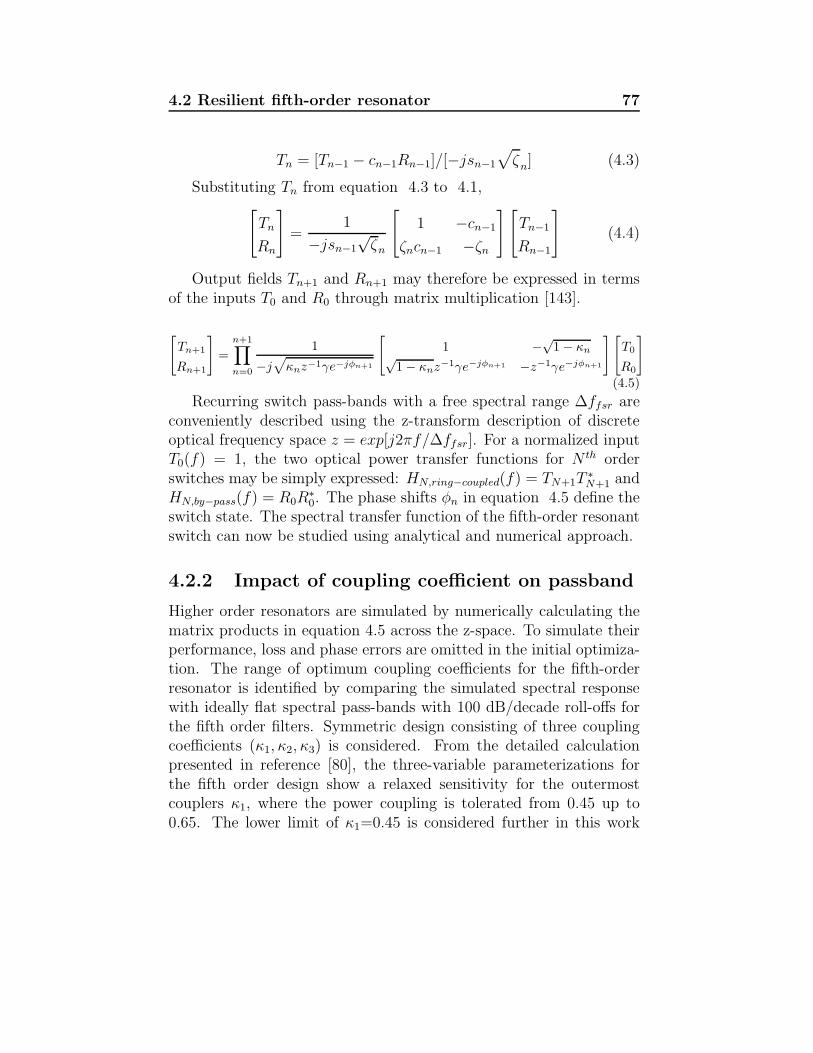
4.2 Resilient fifth-order resonator 77
Tn = [Tn−1 − cn−1Rn−1]/[−jsn−1
√
ζn] (4.3)
Substituting Tn from equation 4.3 to 4.1,[
Tn
Rn
]
=1
−jsn−1
√ζn
[
1 −cn−1
ζncn−1 −ζn
][
Tn−1
Rn−1
]
(4.4)
Output fields Tn+1 and Rn+1 may therefore be expressed in termsof the inputs T0 and R0 through matrix multiplication [143].
[
Tn+1
Rn+1
]
=
n+1∏
n=0
1
−j√
κnz−1γe−jφn+1
[
1 −√1− κn√
1− κnz−1γe−jφn+1 −z−1γe−jφn+1
][
T0
R0
]
(4.5)
Recurring switch pass-bands with a free spectral range ∆ffsr areconveniently described using the z-transform description of discreteoptical frequency space z = exp[j2πf/∆ffsr]. For a normalized inputT0(f) = 1, the two optical power transfer functions for N th orderswitches may be simply expressed: HN,ring−coupled(f) = TN+1T
∗
N+1 andHN,by−pass(f) = R0R
∗
0. The phase shifts φn in equation 4.5 define theswitch state. The spectral transfer function of the fifth-order resonantswitch can now be studied using analytical and numerical approach.
4.2.2 Impact of coupling coefficient on passband
Higher order resonators are simulated by numerically calculating thematrix products in equation 4.5 across the z-space. To simulate theirperformance, loss and phase errors are omitted in the initial optimiza-tion. The range of optimum coupling coefficients for the fifth-orderresonator is identified by comparing the simulated spectral responsewith ideally flat spectral pass-bands with 100 dB/decade roll-offs forthe fifth order filters. Symmetric design consisting of three couplingcoefficients (κ1, κ2, κ3) is considered. From the detailed calculationpresented in reference [80], the three-variable parameterizations forthe fifth order design show a relaxed sensitivity for the outermostcouplers κ1, where the power coupling is tolerated from 0.45 up to0.65. The lower limit of κ1=0.45 is considered further in this work
78 Resilient Higher-order Resonant switch
-2.0
-1.5
-1.0
-0.5
0.0
0 0.02 0.04 0.06 0.08
Tra
nsm
issi
on
(d
B)
k1=0.36
k1=0.405
k1=0.45
k1=0.495
k1=0.54
-2.0
-1.5
-1.0
-0.5
0.0
0 0.02 0.04 0.06 0.08
Tra
nsm
issi
on
(d
B)
k2=0.072
k2=0.081
k2=0.09
k2=0.099
k2=0.108
-2.0
-1.5
-1.0
-0.5
0.0
0 0.02 0.04 0.06 0.08
Tra
nsm
issi
on
(d
B)
k3=0.04
k3=0.045
k3=0.05
k3=0.055
k3=0.06
Absolute frequency normalized to free spectral range |f|/∆ffsr
Figure 4.3: Sensitivity of pass-band transfer function to coupling coefficient in fifthorder resonators. (top) Outermost coupling coefficient κ1, (middle) κ2 and (bot-tom) innermost coefficient κ3 . Transfer functions plotted for the target couplingcoefficients (black) and also for deviations from this value of 0.8 (blue), 0.9 (green),1.1 (yellow) and 1.2 (red) multiples of the target coupling coefficient. The absolutefrequency axis is used to enlarge details for the symmetrical transfer functions.
4.2 Resilient fifth-order resonator 79
to study the most compact directional coupler designs. The corre-sponding optimum inner directional coupler coefficients are κ2=0.09and κ3=0.05. Insight into the critical role of coupling coefficients onthe spectral transfer function is given by plotting transfer functiondetail at the rollover frequency for small independent variations foreach coupler in Fig. 4.3. The first, second and third coupler valuesare varied over the range ±20% in fig. 4.3 top, middle and bottomrespectively.
The outermost couplers in the fifth order design κ1 show a markedimprovement in pass-band ripple as the coupling coefficient value in-creases but this is ultimately at the expense of spectral bandwidthand the physical size. For the second κ2 and third κ3 couplers, a smallincrease in bandwidth is observed as the poles are moved across thepass-band. The optimum values will depend on the target on-statebandwidth.
The propagation of optical signals through the photonic wave-guides leads to changes in phase and amplitude. Phase error leadsto a misalignment of resonances between resonators within the switchelements themselves and also with respect to the input optical dataspectrum. Loss reduces the resonator strength. Propagation impair-ments are studied by introducing systematic and random phase errors into transfer function calculations. From the detailed study shownin [80], systematic errors resulting from a global circuit-level changein refractive index or a detuning of the signal spectrum, lead to a sim-ple linear reduction in the overlap between the designed and achievedbandwidth. The available bandwidth remains at approximately 80%of the original value for fifth-order design. The fourfold improvementin tolerance, compared to the first-order design, results directly fromthe broader, near-rectangular pass-bands for the higher order switches.
Random phase errors occur independently for each resonator andmay represent imperfectly resolved proximity effects in the mask trans-fer during fabrication. The impact of random phase errors with stan-dard deviations exceeding 0.01π for the fifth order rings would impactthe usable bandwidth and diminish the value of higher order resonantdesign if they are not adequately controlled [80].
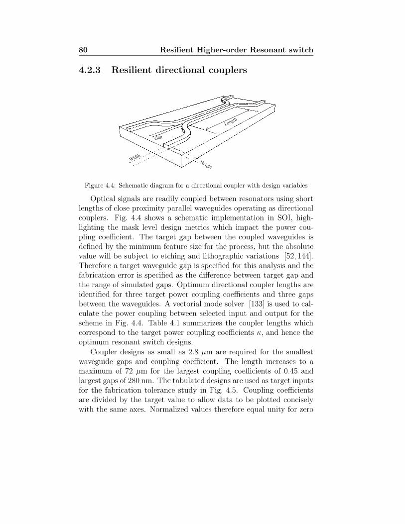
80 Resilient Higher-order Resonant switch
4.2.3 Resilient directional couplers
Figure 4.4: Schematic diagram for a directional coupler with design variables
Optical signals are readily coupled between resonators using shortlengths of close proximity parallel waveguides operating as directionalcouplers. Fig. 4.4 shows a schematic implementation in SOI, high-lighting the mask level design metrics which impact the power cou-pling coefficient. The target gap between the coupled waveguides isdefined by the minimum feature size for the process, but the absolutevalue will be subject to etching and lithographic variations [52, 144].Therefore a target waveguide gap is specified for this analysis and thefabrication error is specified as the difference between target gap andthe range of simulated gaps. Optimum directional coupler lengths areidentified for three target power coupling coefficients and three gapsbetween the waveguides. A vectorial mode solver [133] is used to cal-culate the power coupling between selected input and output for thescheme in Fig. 4.4. Table 4.1 summarizes the coupler lengths whichcorrespond to the target power coupling coefficients κ, and hence theoptimum resonant switch designs.
Coupler designs as small as 2.8 µm are required for the smallestwaveguide gaps and coupling coefficient. The length increases to amaximum of 72 µm for the largest coupling coefficients of 0.45 andlargest gaps of 280 nm. The tabulated designs are used as target inputsfor the fabrication tolerance study in Fig. 4.5. Coupling coefficientsare divided by the target value to allow data to be plotted conciselywith the same axes. Normalized values therefore equal unity for zero
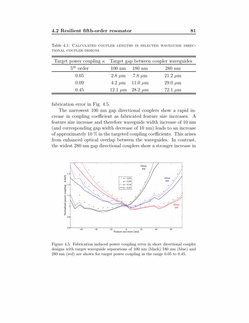
4.2 Resilient fifth-order resonator 81
Table 4.1: Calculated coupler lengths in selected waveguide direc-tional coupler designs
Target power coupling κ Target gap between coupler waveguides
5th order 100 nm 180 nm 280 nm
0.05 2.8 µm 7.8 µm 21.2 µm
0.09 4.2 µm 11.0 µm 29.0 µm
0.45 12.1 µm 28.2 µm 72.1 µm
fabrication error in Fig. 4.5.
The narrowest 100 nm gap directional couplers show a rapid in-crease in coupling coefficient as fabricated feature size increases. Afeature size increase and therefore waveguide width increase of 10 nm(and corresponding gap width decrease of 10 nm) leads to an increaseof approximately 10 % in the targeted coupling coefficients. This arisesfrom enhanced optical overlap between the waveguides. In contrast,the widest 280 nm gap directional couplers show a stronger increase in
−60 −40 −20 0 20 40 600.8
0.9
1
1.1
1.2
1.3
Feature size error [nm]
Nor
mal
ised
pow
er c
oupl
ing
κ/κ(
0)
100nm gap
180nmgap
280nmgap
κ = 0.05κ = 0.09κ = 0.18κ = 0.45
Figure 4.5: Fabrication induced power coupling error in short directional couplerdesigns with target waveguide separations of 100 nm (black) 180 nm (blue) and280 nm (red) are shown for target power coupling in the range 0.05 to 0.45.
82 Resilient Higher-order Resonant switch
coupling for reductions in gap width. This is expected to result fromreductions in effective modal refractive indices for the waveguides. Theintermediate-gap directional couplers show the least sensitivity to theabsolute waveguide separation with a marked reduction in sensitiv-ity to feature size error: ± 30 nm error leads to a 10 % variation inpower coupling. However, the expected feature size variation duringfabrication is greater for 180 nm gap than the 280 nm gap directionalcouplers, and hence the latter is chosen.
4.2.4 Data integrity
The impact of fabrication imperfection on the photonic data integrityis now considered. Broadband optical data signals are representedin frequency space by taking the Fourier transform of non-chirped 10Gbit/second data sequences with 27-1 PRBS. Sampling is performedat the same frequency interval for both the optical data spectrumand the resonant switch transfer function. The product in the fre-quency domain defines the output signal spectrum. A time domainoptical receiver model is implemented with a fifth order Bessel filterand thermal noise defined to give a sensitivity of -20 dBm. To predictpower penalty, the optical power levels which are required to achieveeye-diagram Q-factors of 6 are calculated [145] with and without theresonant switches. The worst case power penalties are recorded forthe full range of directional coupler designs represented in Table 4.1.
Power penalties are plotted in Fig. 4.6 for the conditions wheremean transmission loss does not exceed 2 dB through the ring-coupledpath. To study the role of detuning, the spectra for the input dataand the transfer function are also detuned with respect to one another.For clarity, the role of path length phase error is not considered here,but if inadequately controlled, this would lead to a further bandwidthnarrowing. Worst case power penalties are simulated to be in therange 0.2 dB to 0.7 dB across the on-state pass-bands for all threeorders of resonant switch. A clear correlation is observed betweenthe pass-band ripple and the penalty performance as a function ofsignal detuning. The single peak in the first order response resultsfrom the rounded pass-band and non-optimum optical domain signal
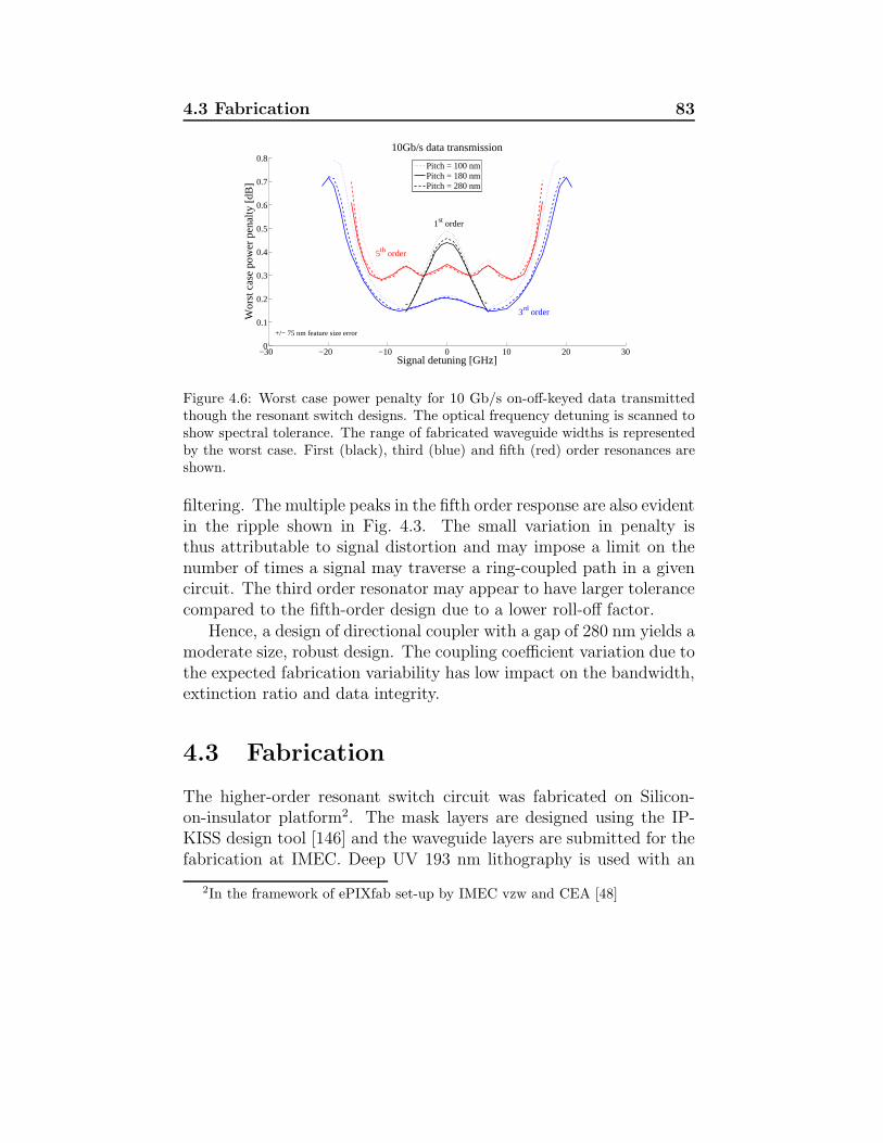
4.3 Fabrication 83
−30 −20 −10 0 10 20 300
0.1
0.2
0.3
0.4
0.5
0.6
0.7
0.810Gb/s data transmission
Signal detuning [GHz]
Wor
st c
ase
pow
er p
enal
ty [d
B]
1st order
3rd order
5th order
+/− 75 nm feature size error
Pitch = 100 nmPitch = 180 nmPitch = 280 nm
Figure 4.6: Worst case power penalty for 10 Gb/s on-off-keyed data transmittedthough the resonant switch designs. The optical frequency detuning is scanned toshow spectral tolerance. The range of fabricated waveguide widths is representedby the worst case. First (black), third (blue) and fifth (red) order resonances areshown.
filtering. The multiple peaks in the fifth order response are also evidentin the ripple shown in Fig. 4.3. The small variation in penalty isthus attributable to signal distortion and may impose a limit on thenumber of times a signal may traverse a ring-coupled path in a givencircuit. The third order resonator may appear to have larger tolerancecompared to the fifth-order design due to a lower roll-off factor.
Hence, a design of directional coupler with a gap of 280 nm yields amoderate size, robust design. The coupling coefficient variation due tothe expected fabrication variability has low impact on the bandwidth,extinction ratio and data integrity.
4.3 Fabrication
The higher-order resonant switch circuit was fabricated on Silicon-on-insulator platform2. The mask layers are designed using the IP-KISS design tool [146] and the waveguide layers are submitted for thefabrication at IMEC. Deep UV 193 nm lithography is used with an
2In the framework of ePIXfab set-up by IMEC vzw and CEA [48]
84 Resilient Higher-order Resonant switch
ICP-RIE dry etch process as a generic foundry platform for photonicintegrated circuits. The design is repeated over the whole 200 mmSOI wafer with a linear exposure dose sweep applied across the wafer.This results in waveguide width variation keeping the pitch constant.The designs are dimensionally identical in each column with the cen-tral column having the designed target waveguide width of 500 nm.This gives an opportunity to test the robustness of the design for fab-rication variations. 1-D surface grating couplers at central wavelength1550 nm are formed by partially etched Si (70 nm) with period 630nm and a filling factor of 0.5 [147]. A top-oxide cladding layer of1200 nm thick SiO2 is applied across the whole 200 mm wafer and thewafer is subsequently diced to complete the foundry service part ofthe fabrication.
The fabricated circuit consists of a 220 nm thick crystalline Si layeron a 2000 nm thick buried oxide substrate. The fifth-order resonantswitch element consists of five coupled resonators with 220 nm×500nm waveguide cross-section, 5 µm bend radius for the curved sectionsand a total path length of 200 µm each. A 500 nm target waveguidewidth is chosen for single mode operation. Directional couplers withconstant target gap of 280 nm and varying lengths (as shown in table4.1) are used. The directional couplers includes a s-bend of length 7µm at the inputs and outputs to suppress unintended spurious cou-pling between the resonator cavities. The total footprint of the switchelement including the MMI crossing is 220 µm×100µm. The sam-ple used in this work is expected to have a waveguide width of 560nm as calculated from the test results provided by IMEC. Thin filmheaters are implemented on individually diced circuits with a multi-mask lithographic process.
4.3.1 Thin-film Heaters
Thin film micro-heaters were created for each switch element by us-ing a four-mask lithographic process. The process was carried outin the COBRA cleanroom at our University. This gives flexibility inthe heater design, fabrication and ensure gold electrodes for ease ofwire-bonding the full circuit. The first mask pattern is used for the
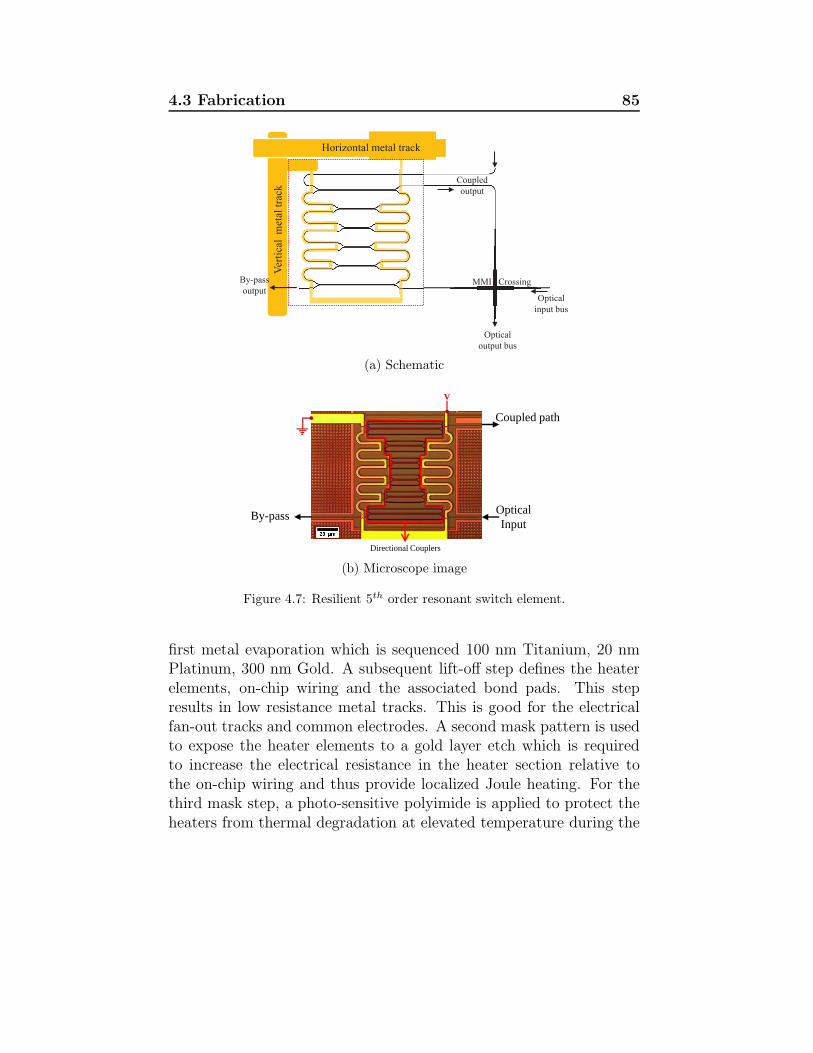
4.3 Fabrication 85
Coupled
output
Optical
input bus
MMI CrossingV
erti
cal
met
al t
rack
By-pass
output
Horizontal metal track
Optical
output bus
(a) Schematic
Optical Input
Coupled path
By-pass
Directional Couplers
V
(b) Microscope image
Figure 4.7: Resilient 5th order resonant switch element.
first metal evaporation which is sequenced 100 nm Titanium, 20 nmPlatinum, 300 nm Gold. A subsequent lift-off step defines the heaterelements, on-chip wiring and the associated bond pads. This stepresults in low resistance metal tracks. This is good for the electricalfan-out tracks and common electrodes. A second mask pattern is usedto expose the heater elements to a gold layer etch which is requiredto increase the electrical resistance in the heater section relative tothe on-chip wiring and thus provide localized Joule heating. For thethird mask step, a photo-sensitive polyimide is applied to protect theheaters from thermal degradation at elevated temperature during the
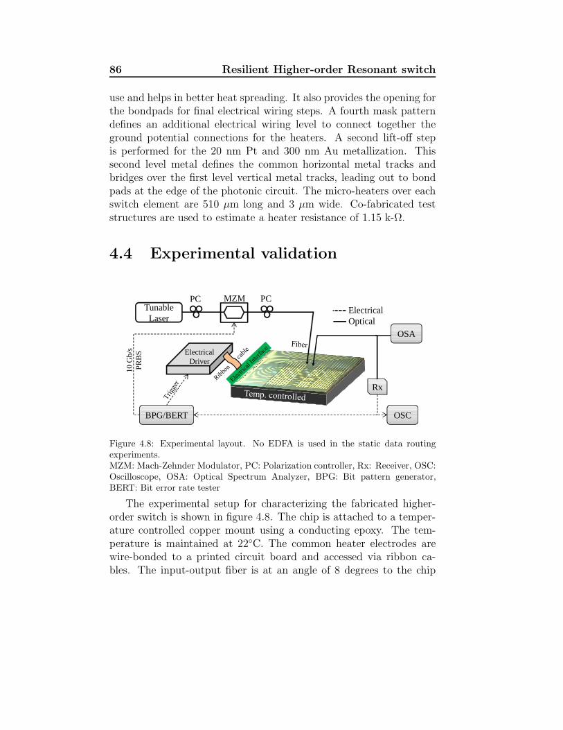
86 Resilient Higher-order Resonant switch
use and helps in better heat spreading. It also provides the opening forthe bondpads for final electrical wiring steps. A fourth mask patterndefines an additional electrical wiring level to connect together theground potential connections for the heaters. A second lift-off stepis performed for the 20 nm Pt and 300 nm Au metallization. Thissecond level metal defines the common horizontal metal tracks andbridges over the first level vertical metal tracks, leading out to bondpads at the edge of the photonic circuit. The micro-heaters over eachswitch element are 510 µm long and 3 µm wide. Co-fabricated teststructures are used to estimate a heater resistance of 1.15 k-Ω.
4.4 Experimental validation
TunableLaser
Rx
MZM PCPC
Electrical Driver
BPG/BERT
10 G
b/s
PR
BS
ElectricalOptical
OSC
OSA
Figure 4.8: Experimental layout. No EDFA is used in the static data routingexperiments.MZM: Mach-Zehnder Modulator, PC: Polarization controller, Rx: Receiver, OSC:Oscilloscope, OSA: Optical Spectrum Analyzer, BPG: Bit pattern generator,BERT: Bit error rate tester
The experimental setup for characterizing the fabricated higher-order switch is shown in figure 4.8. The chip is attached to a temper-ature controlled copper mount using a conducting epoxy. The tem-perature is maintained at 22C. The common heater electrodes arewire-bonded to a printed circuit board and accessed via ribbon ca-bles. The input-output fiber is at an angle of 8 degrees to the chip
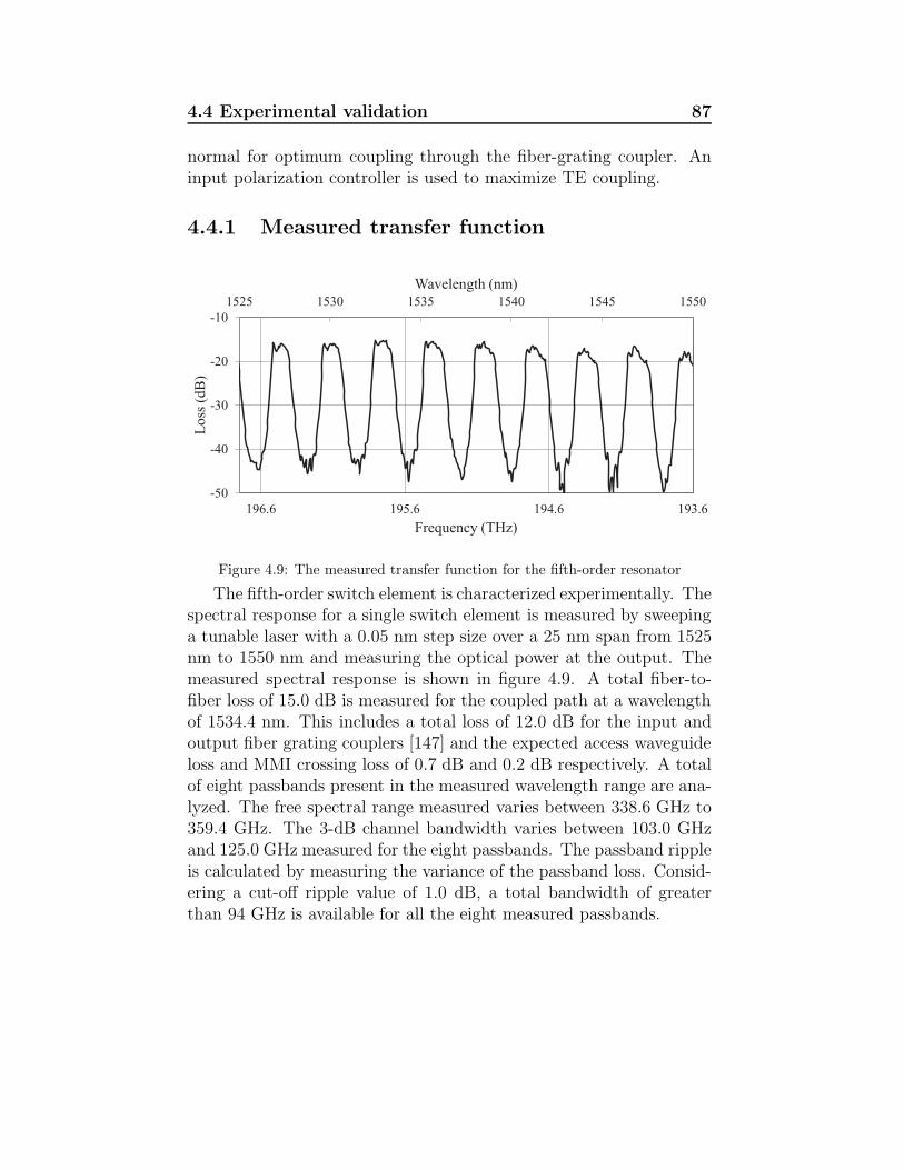
4.4 Experimental validation 87
normal for optimum coupling through the fiber-grating coupler. Aninput polarization controller is used to maximize TE coupling.
4.4.1 Measured transfer function
193.6194.6195.6196.6
-50
-40
-30
-20
-10
1525 1530 1535 1540 1545 1550
Wavelength (nm)
Lo
ss (
dB
)
Frequency (THz)
Figure 4.9: The measured transfer function for the fifth-order resonator
The fifth-order switch element is characterized experimentally. Thespectral response for a single switch element is measured by sweepinga tunable laser with a 0.05 nm step size over a 25 nm span from 1525nm to 1550 nm and measuring the optical power at the output. Themeasured spectral response is shown in figure 4.9. A total fiber-to-fiber loss of 15.0 dB is measured for the coupled path at a wavelengthof 1534.4 nm. This includes a total loss of 12.0 dB for the input andoutput fiber grating couplers [147] and the expected access waveguideloss and MMI crossing loss of 0.7 dB and 0.2 dB respectively. A totalof eight passbands present in the measured wavelength range are ana-lyzed. The free spectral range measured varies between 338.6 GHz to359.4 GHz. The 3-dB channel bandwidth varies between 103.0 GHzand 125.0 GHz measured for the eight passbands. The passband rippleis calculated by measuring the variance of the passband loss. Consid-ering a cut-off ripple value of 1.0 dB, a total bandwidth of greaterthan 94 GHz is available for all the eight measured passbands.
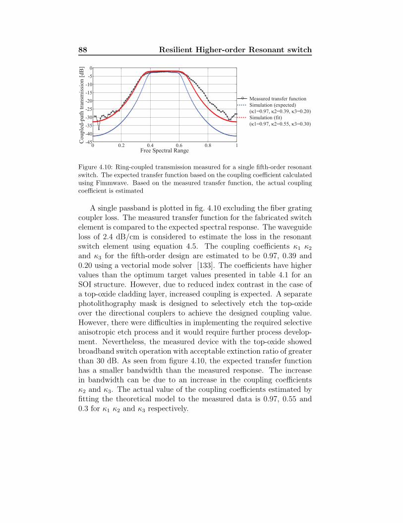
88 Resilient Higher-order Resonant switch
0 0.2 0.4 0.6 0.8 1-45
-40
-35
-30
-25
-20
-15
-10
-5
0
Free Spectral Range
Co
up
led
-pat
h t
ran
smis
sio
n [
dB
]
Measured transfer function
Simulation (expected)
( 1=0.97, 2=0.39, 3=0.20)
Simulation (fit)
( 1=0.97, 2=0.55, 3=0.30)
Figure 4.10: Ring-coupled transmission measured for a single fifth-order resonantswitch. The expected transfer function based on the coupling coefficient calculatedusing Fimmwave. Based on the measured transfer function, the actual couplingcoefficient is estimated
A single passband is plotted in fig. 4.10 excluding the fiber gratingcoupler loss. The measured transfer function for the fabricated switchelement is compared to the expected spectral response. The waveguideloss of 2.4 dB/cm is considered to estimate the loss in the resonantswitch element using equation 4.5. The coupling coefficients κ1 κ2
and κ3 for the fifth-order design are estimated to be 0.97, 0.39 and0.20 using a vectorial mode solver [133]. The coefficients have highervalues than the optimum target values presented in table 4.1 for anSOI structure. However, due to reduced index contrast in the case ofa top-oxide cladding layer, increased coupling is expected. A separatephotolithography mask is designed to selectively etch the top-oxideover the directional couplers to achieve the designed coupling value.However, there were difficulties in implementing the required selectiveanisotropic etch process and it would require further process develop-ment. Nevertheless, the measured device with the top-oxide showedbroadband switch operation with acceptable extinction ratio of greaterthan 30 dB. As seen from figure 4.10, the expected transfer functionhas a smaller bandwidth than the measured response. The increasein bandwidth can be due to an increase in the coupling coefficientsκ2 and κ3. The actual value of the coupling coefficients estimated byfitting the theoretical model to the measured data is 0.97, 0.55 and0.3 for κ1 κ2 and κ3 respectively.
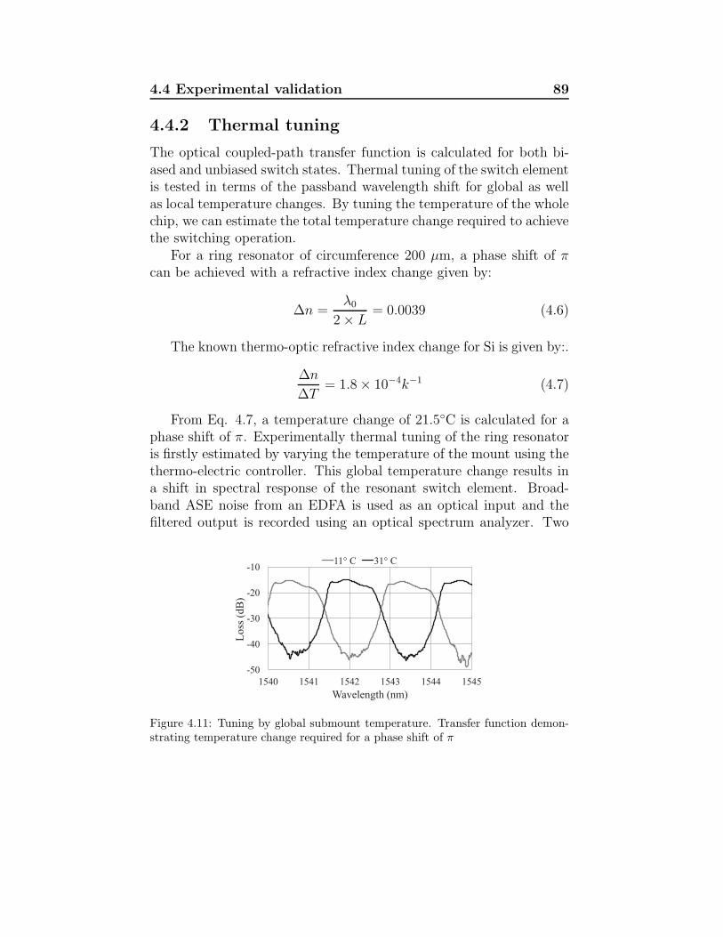
4.4 Experimental validation 89
4.4.2 Thermal tuning
The optical coupled-path transfer function is calculated for both bi-ased and unbiased switch states. Thermal tuning of the switch elementis tested in terms of the passband wavelength shift for global as wellas local temperature changes. By tuning the temperature of the wholechip, we can estimate the total temperature change required to achievethe switching operation.
For a ring resonator of circumference 200 µm, a phase shift of πcan be achieved with a refractive index change given by:
∆n =λ0
2× L= 0.0039 (4.6)
The known thermo-optic refractive index change for Si is given by:.
∆n
∆T= 1.8× 10⁻⁴k−1 (4.7)
From Eq. 4.7, a temperature change of 21.5C is calculated for aphase shift of π. Experimentally thermal tuning of the ring resonatoris firstly estimated by varying the temperature of the mount using thethermo-electric controller. This global temperature change results ina shift in spectral response of the resonant switch element. Broad-band ASE noise from an EDFA is used as an optical input and thefiltered output is recorded using an optical spectrum analyzer. Two
-50
-40
-30
-20
-10
1540 1541 1542 1543 1544 1545
Lo
ss (
dB
)
Wavelength (nm)
11° C 31° C
Figure 4.11: Tuning by global submount temperature. Transfer function demon-strating temperature change required for a phase shift of π
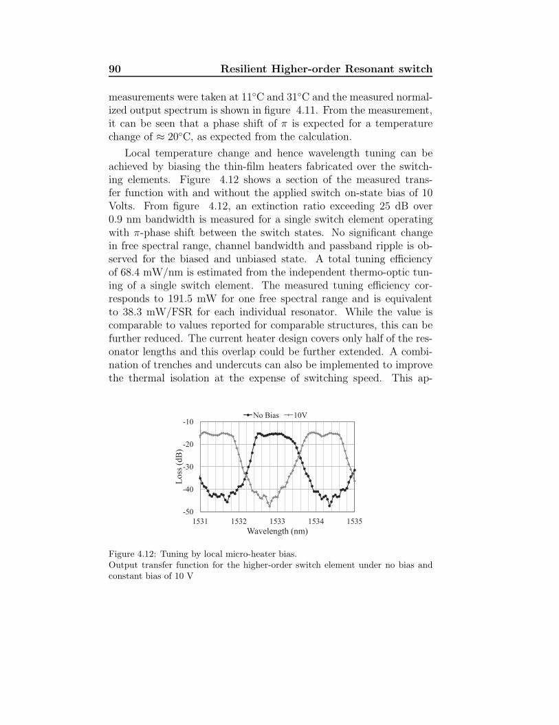
90 Resilient Higher-order Resonant switch
measurements were taken at 11C and 31C and the measured normal-ized output spectrum is shown in figure 4.11. From the measurement,it can be seen that a phase shift of π is expected for a temperaturechange of ≈ 20C, as expected from the calculation.
Local temperature change and hence wavelength tuning can beachieved by biasing the thin-film heaters fabricated over the switch-ing elements. Figure 4.12 shows a section of the measured trans-fer function with and without the applied switch on-state bias of 10Volts. From figure 4.12, an extinction ratio exceeding 25 dB over0.9 nm bandwidth is measured for a single switch element operatingwith π-phase shift between the switch states. No significant changein free spectral range, channel bandwidth and passband ripple is ob-served for the biased and unbiased state. A total tuning efficiencyof 68.4 mW/nm is estimated from the independent thermo-optic tun-ing of a single switch element. The measured tuning efficiency cor-responds to 191.5 mW for one free spectral range and is equivalentto 38.3 mW/FSR for each individual resonator. While the value iscomparable to values reported for comparable structures, this can befurther reduced. The current heater design covers only half of the res-onator lengths and this overlap could be further extended. A combi-nation of trenches and undercuts can also be implemented to improvethe thermal isolation at the expense of switching speed. This ap-
-50
-40
-30
-20
-10
1531 1532 1533 1534 1535
Lo
ss (
dB
)
Wavelength (nm)
No Bias 10V
Figure 4.12: Tuning by local micro-heater bias.Output transfer function for the higher-order switch element under no bias andconstant bias of 10 V
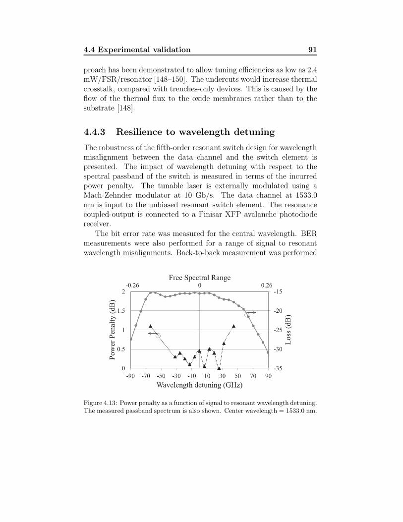
4.4 Experimental validation 91
proach has been demonstrated to allow tuning efficiencies as low as 2.4mW/FSR/resonator [148–150]. The undercuts would increase thermalcrosstalk, compared with trenches-only devices. This is caused by theflow of the thermal flux to the oxide membranes rather than to thesubstrate [148].
4.4.3 Resilience to wavelength detuning
The robustness of the fifth-order resonant switch design for wavelengthmisalignment between the data channel and the switch element ispresented. The impact of wavelength detuning with respect to thespectral passband of the switch is measured in terms of the incurredpower penalty. The tunable laser is externally modulated using aMach-Zehnder modulator at 10 Gb/s. The data channel at 1533.0nm is input to the unbiased resonant switch element. The resonancecoupled-output is connected to a Finisar XFP avalanche photodiodereceiver.
The bit error rate was measured for the central wavelength. BERmeasurements were also performed for a range of signal to resonantwavelength misalignments. Back-to-back measurement was performed
-35
-30
-25
-20
-15
0
0.5
1
1.5
2
-90 -70 -50 -30 -10 10 30 50 70 90
Loss
(dB
)
Pow
er P
enal
ty (
dB
)
Wavelength detuning (GHz)
Free Spectral Range-0.26 0.260
Figure 4.13: Power penalty as a function of signal to resonant wavelength detuning.The measured passband spectrum is also shown. Center wavelength = 1533.0 nm.
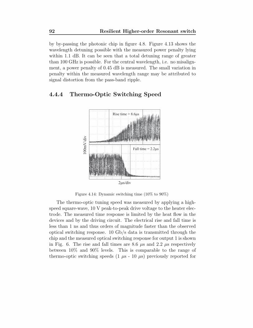
92 Resilient Higher-order Resonant switch
by by-passing the photonic chip in figure 4.8. Figure 4.13 shows thewavelength detuning possible with the measured power penalty lyingwithin 1.1 dB. It can be seen that a total detuning range of greaterthan 100 GHz is possible. For the central wavelength, i.e. no misalign-ment, a power penalty of 0.45 dB is measured. The small variation inpenalty within the measured wavelength range may be attributed tosignal distortion from the pass-band ripple.
4.4.4 Thermo-Optic Switching Speed
2 s/div
10
0m
V/d
iv
Fall time = 2.2 s
Rise time = 8.6 s
Figure 4.14: Dynamic switching time (10% to 90%)
The thermo-optic tuning speed was measured by applying a high-speed square-wave, 10 V peak-to-peak drive voltage to the heater elec-trode. The measured time response is limited by the heat flow in thedevices and by the driving circuit. The electrical rise and fall time isless than 1 ns and thus orders of magnitude faster than the observedoptical switching response. 10 Gb/s data is transmitted through thechip and the measured optical switching response for output 1 is shownin Fig. 6. The rise and fall times are 8.6 µs and 2.2 µs respectivelybetween 10% and 90% levels. This is comparable to the range ofthermo-optic switching speeds (1 µs - 10 µs) previously reported for
4.5 Summary 93
single order microring resonators [149, 150].
4.5 Summary
A fifth-order resonant switch is presented as a resilient broadbandcrossbar compliant wavelength selective element. Design parametersare presented for SOI using moderate size directional couplers of upto 20 µm. This approach offers simultaneous relaxation of fabrica-tion tolerance and decoupling of off-state extinction from on-statebandwidth. Variation in the coupling coefficients and their impacton data integrity has been presented as a function of fabrication error.Thermo-optic switching is achieved by fabricating a single thin-filmheater over the resonant switch element. Low penalty of less than 1.1dB is observed for wavelength detuning of greater than ± 50 GHz, in-dicating robustness to wavelength misalignments. With an extinctionratio of more than 25 dB achievable per element, the fifth-order reso-nant switch proves to be a viable candidate for large scale broadbandhigh-connectivity monolithic switching networks.
In the next chapter, these higher-order switch elements are cas-caded to form an optical crossbar switch matrix. Data routing ispresented for static 1×4 and 2×2 operation as well as dynamic switchoperation. Data integrity for the routed signal is presented in termsof the circuit level metrics of loss, crosstalk and optical power penaltyfor the measured paths.

5Optical Crossbar Switch
Matrix
In this chapter1, a crossbar switch matrix with integrated thin-filmheaters for each higher-order resonant switch element is characterizedfor the first time. A common addressing scheme is used for each rowand column to reduce the required number of electrical connections.The crossbar switch is analyzed with four switch elements on a grid oforthogonal input and output bus waveguides to achieve 1×4 and 2×2functionality. The power penalty and the crosstalk are assessed forall the measured outputs. Bit-error-rate measurements for dynamicoperation are also reported.
5.1 Introduction
To take the next step towards scalable, high-density, high-connectivityoptical switch matrix design, there is a need to develop architec-tures which allow a large number of high-bandwidth, small-footprintswitch elements to be electronically and photonically connected in thesame monolithic circuit. As shown in Chapter 4, higher-order micro-resonators are attractive for optical signal routing, providing broad-band and flat-topped transmission, good out-of-band signal extinction
1Based on the results published in [136, 137]
96 Optical Crossbar Switch Matrix
and tolerance to wavelength misalignment. As summarized in Chap-ter 1 (Table 1.2), various crossbar switch configurations consisting ofhigher-order resonant switches are proposed for a large scale switchmatrix. However, so far only single switch elements have been charac-terized [93–95]. No characterization has been performed to quantifythe data integrity for multiple bus-coupled higher-order switches [92].
There are mainly two factors which inhibit the use of the proposedhigher-order resonant switches in a larger switch matrix. Firstly, mostof the switches reported in the literature (Table 1.2) use carrier in-jection (optical or electrical) for switching. Though this results inswitching speed in the order of nanoseconds, it fails to provide thenecessary tuning to compensate for the wavelength registration er-rors of the order of 1 nm resulting from nano-scale feature-size vari-ability between the switch elements [52]. Full tuning is most readilyachieved using modest sized thermo-optic phase shifters. The secondrestraining factor in matrix implementation is the number of controlelectrodes associated with a large matrix. By using the resilient fifth-order switch, only a single heater is required per element. This stillmeans that a crossbar matrix with N×N elements will require N2+1connections. This problem is tackled by using an electronic matrixaddressing scheme.
In this chapter, design and characterization of a crossbar switchmatrix is presented. It comprises of broadband 1×2 fifth-order reso-nant switch elements demonstrated in the last chapter. The connec-tion from the input bus to any given output waveguide is made bythermo-optical tuning of the intersecting high-order switch elementto route signals through the ring-coupled path. The connection islikewise broken by tuning the switch to route to the by-pass path.Performance of the crossbar switch is characterized and presented interms of the circuit level metrics of loss, crosstalk and optical powerpenalty for 1×4 (Section 5.3.1), 2×2 (Section 5.3.2) and dynamic rout-ing operation (Section 5.3.3).
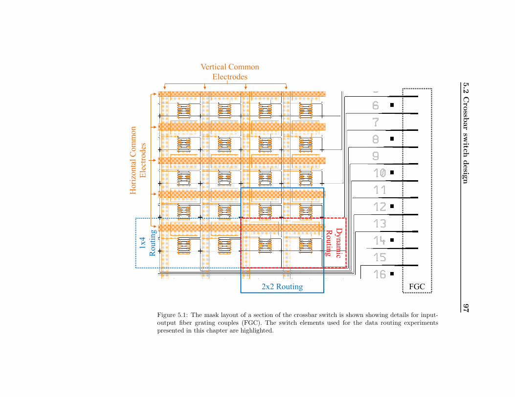
5.2
Cro
ssbarsw
itchdesig
n97
1x
4
Ro
uti
ng
2x2 Routing
Dy
nam
ic
Ro
utin
g
FGC
Ho
rizo
nta
l C
om
mo
n
Ele
ctro
des
Vertical Common
Electrodes
Figure 5.1: The mask layout of a section of the crossbar switch is shown showing details for input-output fiber grating couples (FGC). The switch elements used for the data routing experimentspresented in this chapter are highlighted.
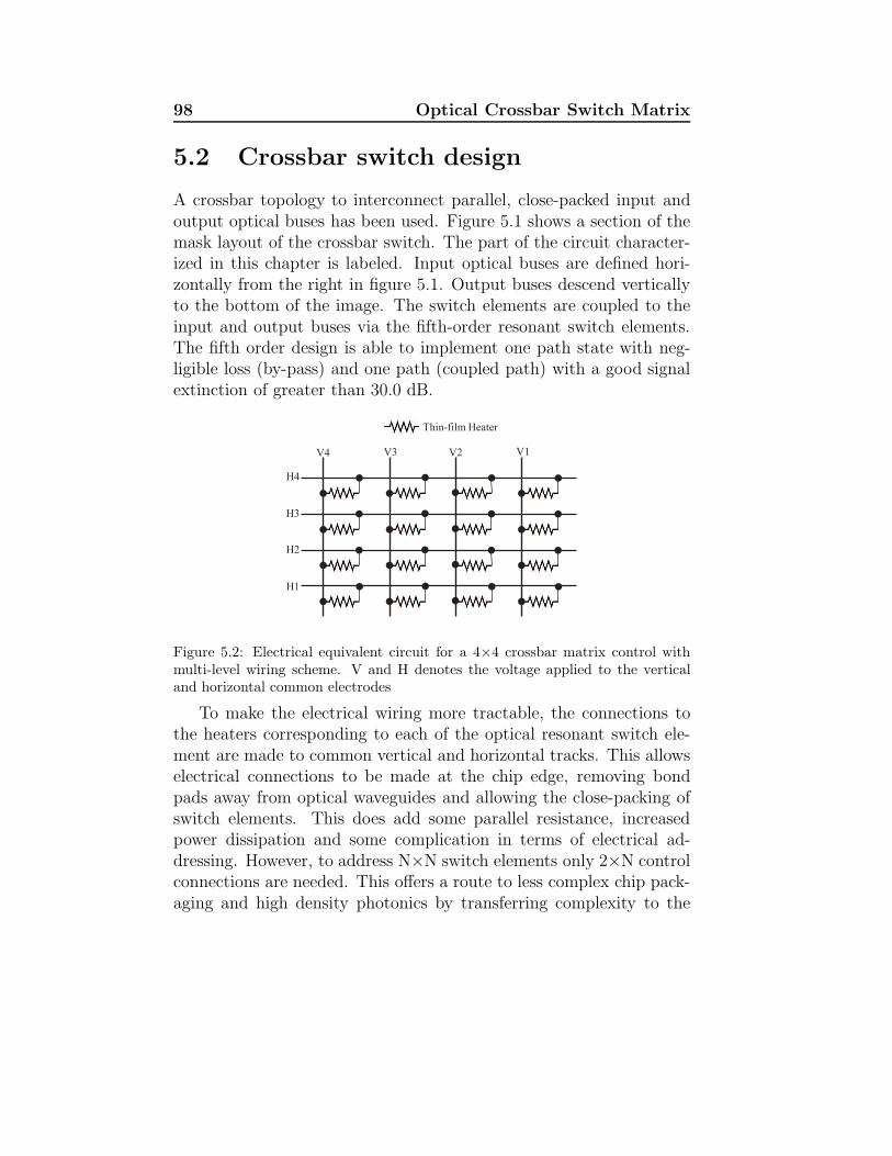
98 Optical Crossbar Switch Matrix
5.2 Crossbar switch design
A crossbar topology to interconnect parallel, close-packed input andoutput optical buses has been used. Figure 5.1 shows a section of themask layout of the crossbar switch. The part of the circuit character-ized in this chapter is labeled. Input optical buses are defined hori-zontally from the right in figure 5.1. Output buses descend verticallyto the bottom of the image. The switch elements are coupled to theinput and output buses via the fifth-order resonant switch elements.The fifth order design is able to implement one path state with neg-ligible loss (by-pass) and one path (coupled path) with a good signalextinction of greater than 30.0 dB.
V1V2V3V4
H1
H2
H3
H4
Thin-film Heater
Figure 5.2: Electrical equivalent circuit for a 4×4 crossbar matrix control withmulti-level wiring scheme. V and H denotes the voltage applied to the verticaland horizontal common electrodes
To make the electrical wiring more tractable, the connections tothe heaters corresponding to each of the optical resonant switch ele-ment are made to common vertical and horizontal tracks. This allowselectrical connections to be made at the chip edge, removing bondpads away from optical waveguides and allowing the close-packing ofswitch elements. This does add some parallel resistance, increasedpower dissipation and some complication in terms of electrical ad-dressing. However, to address N×N switch elements only 2×N controlconnections are needed. This offers a route to less complex chip pack-aging and high density photonics by transferring complexity to the
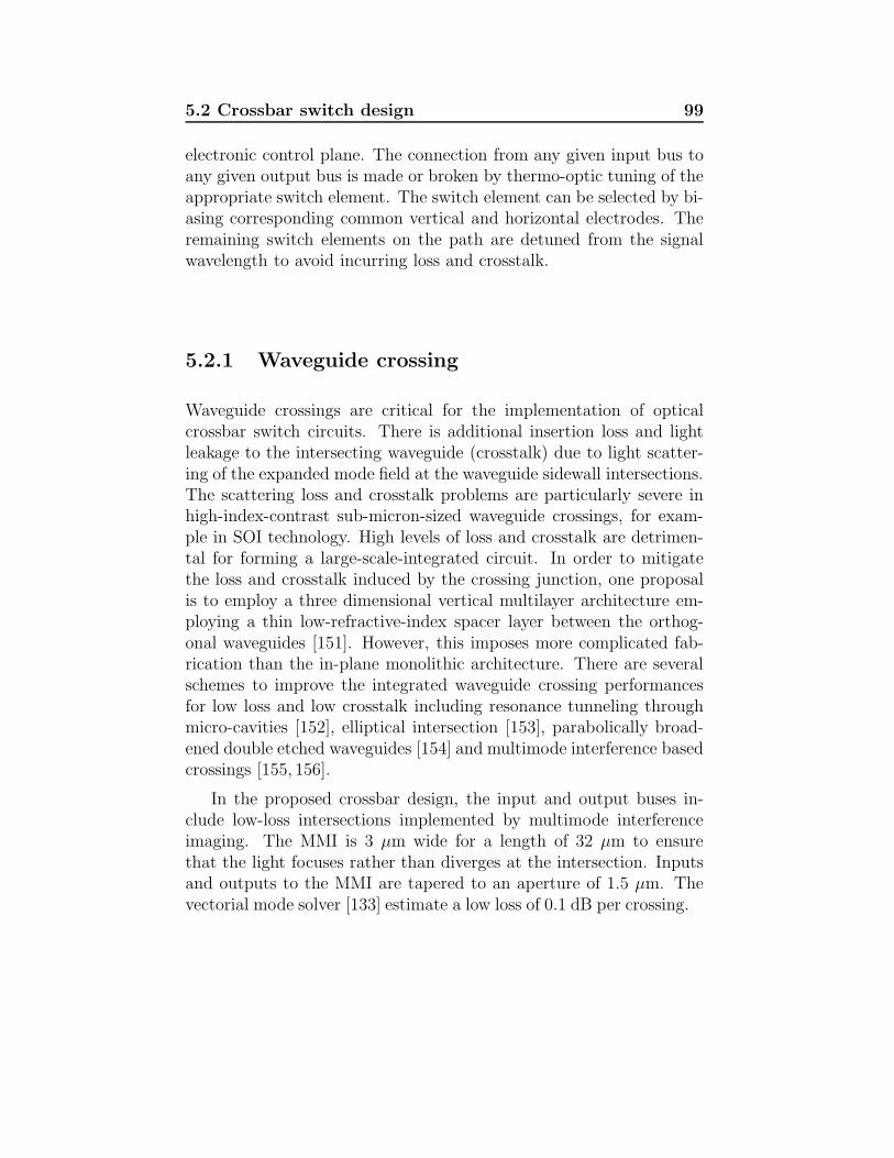
5.2 Crossbar switch design 99
electronic control plane. The connection from any given input bus toany given output bus is made or broken by thermo-optic tuning of theappropriate switch element. The switch element can be selected by bi-asing corresponding common vertical and horizontal electrodes. Theremaining switch elements on the path are detuned from the signalwavelength to avoid incurring loss and crosstalk.
5.2.1 Waveguide crossing
Waveguide crossings are critical for the implementation of opticalcrossbar switch circuits. There is additional insertion loss and lightleakage to the intersecting waveguide (crosstalk) due to light scatter-ing of the expanded mode field at the waveguide sidewall intersections.The scattering loss and crosstalk problems are particularly severe inhigh-index-contrast sub-micron-sized waveguide crossings, for exam-ple in SOI technology. High levels of loss and crosstalk are detrimen-tal for forming a large-scale-integrated circuit. In order to mitigatethe loss and crosstalk induced by the crossing junction, one proposalis to employ a three dimensional vertical multilayer architecture em-ploying a thin low-refractive-index spacer layer between the orthog-onal waveguides [151]. However, this imposes more complicated fab-rication than the in-plane monolithic architecture. There are severalschemes to improve the integrated waveguide crossing performancesfor low loss and low crosstalk including resonance tunneling throughmicro-cavities [152], elliptical intersection [153], parabolically broad-ened double etched waveguides [154] and multimode interference basedcrossings [155, 156].
In the proposed crossbar design, the input and output buses in-clude low-loss intersections implemented by multimode interferenceimaging. The MMI is 3 µm wide for a length of 32 µm to ensurethat the light focuses rather than diverges at the intersection. Inputsand outputs to the MMI are tapered to an aperture of 1.5 µm. Thevectorial mode solver [133] estimate a low loss of 0.1 dB per crossing.
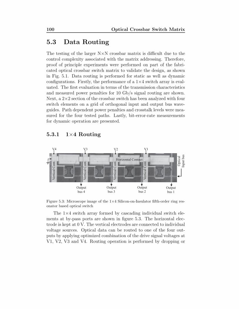
100 Optical Crossbar Switch Matrix
5.3 Data Routing
The testing of the larger N×N crossbar matrix is difficult due to thecontrol complexity associated with the matrix addressing. Therefore,proof of principle experiments were performed on part of the fabri-cated optical crossbar switch matrix to validate the design, as shownin Fig. 5.1. Data routing is performed for static as well as dynamicconfigurations. Firstly, the performance of a 1×4 switch array is eval-uated. The first evaluation in terms of the transmission characteristicsand measured power penalties for 10 Gb/s signal routing are shown.Next, a 2×2 section of the crossbar switch has been analyzed with fourswitch elements on a grid of orthogonal input and output bus wave-guides. Path dependent power penalties and crosstalk levels were mea-sured for the four tested paths. Lastly, bit-error-rate measurementsfor dynamic operation are presented.
5.3.1 1×4 Routing
Op
tica
l
Inp
ut
bus
Output
bus 1
Output
bus 2
V2 V1
Horizontal Contact
Ver
tica
l C
ont.
Ver
tica
l C
ont.
Ver
tica
l C
ont.
Ver
tica
l C
ont.
V4 V3
Output
bus 3
Output
bus 4
Figure 5.3: Microscope image of the 1×4 Silicon-on-Insulator fifth-order ring res-onator based optical switch
The 1×4 switch array formed by cascading individual switch ele-ments at by-pass ports are shown in figure 5.3. The horizontal elec-trode is kept at 0 V. The vertical electrodes are connected to individualvoltage sources. Optical data can be routed to one of the four out-puts by applying optimized combination of the drive signal voltages atV1, V2, V3 and V4. Routing operation is performed by dropping or
5.3 Data Routing 101
passing the data channel at the desired output by the fifth-order res-onant switch element. The experimental layout is shown in figure 4.8.The electrical driver consists of four independent voltage sources. Atunable laser operating at a wavelength of 1534.4 nm is externallymodulated at 10 Gb/s with a pseudo random bit sequence of 231-1 bitlengths. The data channel is input to the 1×4 switch with -3.1 dBmin-fiber input power. The 1×4 switch optical outputs are accessed oneby one and connected directly to a Finisar XFP avalanche photodiodereceiver.
0Output 1 Output 2 Output 3 Output 4
-30
-15
ss (
dB
)
Crosstalk
>25dB
-45
Lo
s >25dB
-60
1 2 3 4
ON-state Switch Element
Figure 5.4: Measured crosstalk for the 1×4 switch for all outputs.
In this experiment, the 1×4 switch was operated with minimumdrive voltages required for maximum transmission through each ofthe four selected output port. This is done by detuning the precedingswitch elements to minimize coupling into an undesired output port.For output 1 and output 3, V1 and V3 are biased at 10 V and 6 Vrespectively to get maximum coupled output power. For output 2, V1and V2 are biased at 13.35 V and 6.8 V respectively. However, for out-put 4 careful voltage adjustments are required to minimize crosstalkand maximize the output. V1, V2, V3 and V4 were biased at 16.1 V,14.0 V, 11.2 V and 14.15 V respectively. The voltage values mentionedand used in this experiment are not optimized to minimize crosstalkat all four ports. The switch can operate with crosstalk better than25 dB for all ports under optimized bias conditions as shown in fig-
102 Optical Crossbar Switch Matrix
-60
-50
-40
-30
-20
-10
1532 1533 1534 1535 1536
Lo
ss (
dB
)
Wavelength (nm)
Output 1Output 2Output 3Output 4
Figure 5.5: Overlapped output transfer function for all the outputs under dc biaswith voltages optimized for minimum coupled path loss.The vertical red dotted line denotes the test wavelength used.
ure 5.4. To achieve this crosstalk value, all the un-desired switchesmust be tuned off-resonance.
The transfer function for all four ports is shown in figure 5.5. Fiber-to-fiber losses of 15.0 dB, 16.4 dB, 16.9 dB and 18.2 dB are measuredfor outputs 1, 2, 3 and 4 respectively when the preceding switch ele-ments are detuned relative to the test signal. These losses are expectedto include a contribution of 12 dB for the input and output fiber grat-ing couplers, 0.7-1.1 dB for the access waveguide loss for both inputand outputs. 0.2-0.5 dB for total MMI crossing losses and a waveguide
Back-to-back10-3
Rat
e
Output 1Output 2Output 3
it E
rror
pOutput 4
10-6
B
10-9
-33 -32 -31 -30 -29 -28 -27 -26 -25Mean received power (dBm)p ( )
Figure 5.6: Measured bit error rate for the 1×4 switch for all outputs.
5.3 Data Routing 103
loss of 2.4 dB/cm. While 1.8 dB loss may be attributable to bend andwaveguide loss in the resonant switch element, totalling to an excessloss of less than 0.55 dB.
The bit error rate measured for each output under static bias con-dition is shown in figure 5.6. From the bit error rate plots, a powerpenalty of 0.25 dB is measured for output 1. Negative penalties of0.2 dB, 0.15 dB and 0.7 dB are observed for output 2, output 3 andoutput 4 respectively. The origins of this apparent signal improve-ment are unclear. The laser relative intensity noise is very low at -160dB/Hz and there is no additional source of optical noise or off-chipfiltering. The data modulator extinction ratio is measured to be 10.4dB. One possibility may be the interaction of the preceding switchelements with the optical data leading to signal reshaping. The pre-cise value of power penalty is observed to be critically sensitive to theprecise bias conditions.
5.3.2 2×2 Routing
The 2×2 crossbar switch, shown in Fig. 5.7, is assessed by connect-ing the two vertical common electrodes to the voltage supply V1 andV2. The two horizontal common electrodes are kept at 0 V. Thedrive voltages are optimized for minimum path loss and crosstalk fora wavelength 1544.2 nm.
Table 5.1: Bias condition and measured crosstalk for 2×2 routing.
Path measured On-chipVoltage applied(Volts)
Crosstalk
loss(dB) V1 V2
Input 1 to Output 1 3.0 3.0 6.6 36.0
Input 1 to Output 2 4.5 11.1 13.0 25.5
Input 2 to Output 1 4.0 7.6 10.0 33.3
Input 2 to Output 2 5.5 2.3 5.9 20.5
104 Optical Crossbar Switch Matrix
The voltage configuration for each path is summarized in Table 5.1.The spectral transfer functions from inputs 1 and 2 to outputs 1 and 2are shown in figure 5.8. A relative spectral misalignment is suspectedbetween the individual resonant switch elements and this may leadto pass-band narrowing and distortion as observed in the measuredspectrum for paths with more than one switch elements. The com-mon addressing scheme introduces some interdependence and furtheroptimizations may also be feasible using four control lines. In thisexperiment, the path input 1 to output 1 is enabled by biasing V1and V2 at 3 V and 6.6 V respectively. This tunes the switch elementto the signal wavelength on input bus 1 to maximize coupled-path op-tical power to output bus 1. To make the connection from input 2 tooutput 1, the first switch element is tuned to off-state and the secondswitch is tuned to the on-state. This is achieved by setting V1 at thehigher voltage of 7.6 V. The apparent scatter in the voltage values inTable 5.1 reflects the spread in wavelength registration for the unbi-
V1V2
Optical input
bus 2bus 2
Optical input
O i l
p p
bus 1
O ti l Optical
output bus 1
Optical
output bus 2
Figure 5.7: Microscope image of a crossbar switch. The optical input and outputbuses are separated by 250µm and 300µm respectively.
5.3 Data Routing 105
ased switch elements. The on-state losses are observed to vary from15.0 dB to 17.5 dB. This value is expected to include 12.0 dB fromfiber-to-chip coupling at both input and output. For clarity, this valueis subtracted for the estimated losses in Table 5.1. Waveguide lossesare expected to be of order 2.4 dB/cm, allowing a direct estimate ofbus losses and an indirect estimate of the switch element loss [80].Straight access waveguide losses are expected to vary from 0.7 dB to1.0 dB. Mode propagation calculations indicate total crossing lossesfrom 0.2 dB to 0.4 dB for the four paths and 1.8 dB for the on-stateswitch elements. The small excess loss of only 0.3 dB to 0.65 dB islikely attributable to off-state losses of imperfectly detuned switch el-ements. The extinction ratio is measured directly at a wavelengthof 1544.2 nm for the on and off states. This varies from 20.5 dB to36.0 dB. This best case extinction is in-line with expectations for therealized design and represents a path with just one switch element.The worst case value involves a path with one on-state switch and twooff-state switches and may indicate a need for further optimizationsfor the switch elements in the off-state.
Routing experiments are performed for all four paths to quantify10 Gb/s data signal integrity. The experimental layout is identical
-50
-40
-30
-20
-10
1543 1544 1545 1546
Loss
(dB
)
Wavelength (nm)
Input 1 - Output 1
Input 1 - Output 2
Input 2 - Output 1
Input 2 - Output 2
Figure 5.8: Spectral transfer function of all four paths under dc bias. The verticalred dotted line denotes the test wavelength used.
106 Optical Crossbar Switch Matrix
Back-to-back
Input 1 - Output 1
I 1 O 210-3
ror
Rat
e Input 1 - Output 2
Input 2 - Output 1
Input 2 - Output 2
Bit
Err
p p
10-6
10-9
-33 -31 -29 -27 -25 -23
10-9
33 31 29 27 25 23
Mean received power (dBm)
Figure 5.9: Measured bit error rate for the 2×2 switch for all measured paths.
to the last section. The transmitter comprises a tunable laser whichis externally modulated using a MZM with a 231 − 1 pseudo randombit sequence. No optical amplification is needed or used. The datachannel is input to the crossbar switch with an in-fiber input powerof -2 dBm. The bit error rate is measured for each of the four pathsfor conditions shown in Table 5.1. Bit error rate plots are shown infigure 5.9. A logarithmic relationship is observed with no error floor.The power penalty is measured to be negligible for the best case path.The worst case power penalty of 1.5 dB is measured for input 1 tooutput 2. There is a high level of ripple observed in the correspondingpass-band but there is no clear correlation between the amplitudevariations in the optical transfer functions shown in Figure 5.8 andthe power penalties observed in Figure 5.9. This may indicate a morecomplex dispersion-related cause for signal degradation. This may alsobe a further symptom of the imperfectly spectrally-alignment switchelements.
5.3.3 Dynamic Routing
Dynamically reconfigured routing is studied for optical signals routedfrom the bus input to the first two output waveguides. Figure 4.8shows the configuration of bit error rate test equipment, the electri-
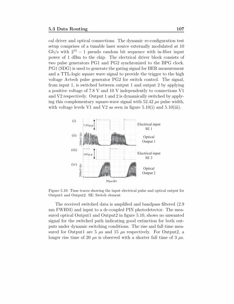
5.3 Data Routing 107
cal driver and optical connections. The dynamic re-configuration testsetup comprises of a tunable laser source externally modulated at 10Gb/s with 215 − 1 pseudo random bit sequence with in-fiber inputpower of 1 dBm to the chip. The electrical driver block consists oftwo pulse generators PG1 and PG2 synchronized to the BPG clock.PG1 (SDG) is used to generate the gating signal for BER measurementand a TTL-logic square wave signal to provide the trigger to the highvoltage Avtech pulse generator PG2 for switch control. The signal,from input 1, is switched between output 1 and output 2 by applyinga positive voltage of 7.8 V and 10 V independently to connections V1and V2 respectively. Output 1 and 2 is dynamically switched by apply-ing this complementary square-wave signal with 52.42 µs pulse width,with voltage levels V1 and V2 as seen in figure 5.10(i) and 5.10(iii).
Electrical input
SE 1
Electrical input
SE 2
Optical
Output 1
Optical
Output 2
(i)
(ii)
(iii)
(iv)
20
0m
V/d
iv2
00
mV
/div
20µs/div
10Vp-p
7.8Vp-p
Figure 5.10: Time traces showing the input electrical pulse and optical output forOutput1 and Output2. SE: Switch element
The received switched data is amplified and bandpass filtered (2.9nm FWHM) and input to a dc-coupled PIN photodetector. The mea-sured optical Output1 and Output2 in figure 5.10, shows no unwantedsignal for the switched path indicating good extinction for both out-puts under dynamic switching conditions. The rise and fall time mea-sured for Output1 are 5 µs and 15 µs respectively. For Output2, alonger rise time of 20 µs is observed with a shorter fall time of 3 µs.
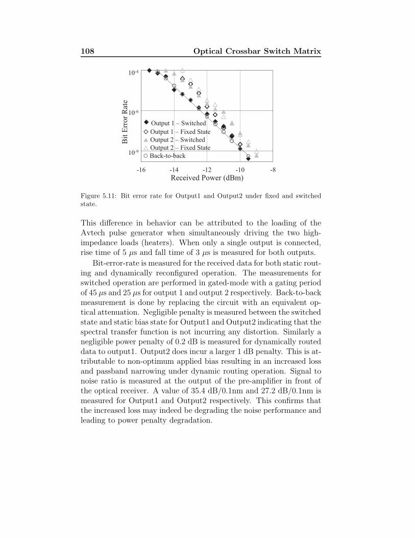
108 Optical Crossbar Switch Matrix
-16 -14 -12 -10 -8
Bit
Err
or
Rat
e
Received Power (dBm)
10-9
10-6
10-4
Output 1 – Switched
Output 1 – Fixed State
Output 2 – Switched
Output 2 – Fixed State
Back-to-back
Figure 5.11: Bit error rate for Output1 and Output2 under fixed and switchedstate.
This difference in behavior can be attributed to the loading of theAvtech pulse generator when simultaneously driving the two high-impedance loads (heaters). When only a single output is connected,rise time of 5 µs and fall time of 3 µs is measured for both outputs.
Bit-error-rate is measured for the received data for both static rout-ing and dynamically reconfigured operation. The measurements forswitched operation are performed in gated-mode with a gating periodof 45 µs and 25 µs for output 1 and output 2 respectively. Back-to-backmeasurement is done by replacing the circuit with an equivalent op-tical attenuation. Negligible penalty is measured between the switchedstate and static bias state for Output1 and Output2 indicating that thespectral transfer function is not incurring any distortion. Similarly anegligible power penalty of 0.2 dB is measured for dynamically routeddata to output1. Output2 does incur a larger 1 dB penalty. This is at-tributable to non-optimum applied bias resulting in an increased lossand passband narrowing under dynamic routing operation. Signal tonoise ratio is measured at the output of the pre-amplifier in front ofthe optical receiver. A value of 35.4 dB/0.1nm and 27.2 dB/0.1nm ismeasured for Output1 and Output2 respectively. This confirms thatthe increased loss may indeed be degrading the noise performance andleading to power penalty degradation.
5.4 Discussion 109
5.4 Discussion
The crossbar architecture enables a simple scalable solution for in-tegration. The tradeoff, however, is the insertion loss and crosstalkat the waveguide crossing which may eventually limit the scalabil-ity. Therefore, the key is to use a low-loss low-crosstalk waveguidecrossing. The common addressing scheme using multi-level metalliza-tion is used for the first time to reduce the number of connections.While the common matrix addressing scheme is not completely ro-bust to wavelength-registration errors observed in the current circuitand would require simpler electronic control if the resonant switcheswere spectrally aligned in the off-state. It has nevertheless enabledseveral proof of principle experiments to be performed. It does re-quire a more sophisticated control and calibration scheme and it is anarea of on-going research.
The voltages used are relatively high with respect to state of theart. However it should be noted that five coupled resonators are si-multaneously tuned with a series connected heater element, and thevoltage can be reduced significantly with parallel connection. The re-quirement to actuate several switches at the same time for the besttransmission performance is non-ideal. This results from a combina-tion of effects. Wavelength alignment errors attributable to nanome-ter scale feature size variation are comparable to the free spectral andtherefore off-state voltages are non-zero for the switches.
5.5 Summary
A crossbar switch matrix is demonstrated based on fifth-order resonantelements on a grid of orthogonal input and output bus waveguides. Toallow connectivity scaling, the use of multi-level metal and a commonaddressing scheme is explored. 1×4 switching with power penalty ofless than 0.25 dB is measured for all four ports tested. Crosstalk ofbetter than 25 dB is achievable. 2×2 switching is demonstrated withcrosstalk suppression of 20 dB to 36 dB, on-chip losses of 3.0 to 5.5 dBand modest power penalty from 0.0 dB to 1.5 dB. Finally, dynamic

110 Optical Crossbar Switch Matrix
re-configuration is presented with 20 µs switching time and worst-casemeasured power penalty of 1 dB. This is extremely encouraging forfurther connectivity scaling.
6Conclusions
The main objective of this work was to demonstrate system-level wave-length agile switching functionalities in PICs. This work has achievedsignificant milestones towards scalable, high-bandwidth, robust large-scale switch circuits. The SOA gated cyclic AWG based space andwavelength select architecture, exploited in this work, has demon-strated crucial characteristics including co- and counter propagatingmulti-data-rate routing. The ability to route multi-channels simulta-neously increases the end-to-end bandwidth, reducing the energy perbit. The capability of the switch fabric to handle bi-directional traf-fic can provide flexibility and robustness to the network. Moreover,on-the-fly routing can assist in reducing the switch node complexity.With the attained nanosecond reconfiguration speed, this is importantto realize future packet switching applications.
The SOI platform is explored to increase the switch density. Aresilient broadband higher-order resonant switch is designed to elim-inate the intrinsic trade-off between bandwidth and extinction ratioin the single-order resonant switches. The design uses a combina-tion of unconventionally large circumference resonators in combina-tion with fabrication tolerant directional couplers and thermo-optictuning. This ensures a degree of resilience to fabrication variations,and also the means to compensate phase error by means of maximumphase modulation of 2π. Multi-level metallization is used to reducethe number of control electrodes for co-fabricated thin-film heaters.

112 Conclusions
This work has successfully demonstrated the feasibility of the design.Proof-of-concept circuit demonstration has shown great potential forfull crossbar matrix implementation.
The role of InP and SOI based circuits are evaluated on the basisof the results described in this thesis. Some key parameters, whichare critical for future large-scale switch implementation, are presentedbelow.
On-chip Loss
Due to the high-index contrast in SOI, smaller waveguide bends areachievable and hence the total size of the circuit is smaller than InP.Moreover, waveguide propagation loss is lower at 2.4 dB/cm comparedto 3.5–4.5 dB/cm for shallow and deep-etched InP waveguide respec-tively. However, SOAs in the InP-based circuits can easily compensatefor this small difference in waveguide loss. The main advantage of theInP cross-connect design is the uniformity in the path loss. The differ-ence in the path loss for the best and worst case only depends on thenumber of crossings and the AWG transfer function. But in the caseof the crossbar architecture, the difference in the shortest and longestpath loss can be significant. Thus, it may require power equalizationfor system implementation.
Extinction ratio
The switches must have high extinction ratio to minimize crosstalk inthe circuit. It has been observed that SOA can provide an extinctionratio greater than 40 dB between on and off state. In the SOI circuit,the fifth-order resonant switch is shown to have extinction ratio betterthan 25 dB. In principle, it is possible to have extinction ratio betterthan 60 dB for the fifth-order resonator design [80].
Bandwidth
The maximum data rate that can be routed through the circuit isdependent on the WSS passband. Comparable 3-dB bandwidth of
113
greater than 100 GHz is measured both for the AWG and the fifth-order resonant WSS. Flat-top response for the latter is favorable forlarge bandwidth signals. However, it is straightforward to design flat-topped AWGs, although with additional insertion loss.
Connectivity
The InP cross-connect allows increased system connectivity, flexibilityand end-to-end bandwidth by exploiting the cyclic AWG. The archi-tecture allows broadcast to multiple output ports. On the other hand,the SOI high-density crossbar matrix only permits unicast operation.
Polarization dependence
Polarization can play an important role in the case of InP circuitsdue to the dependence of SOA gain on the input polarization. Po-larization rotation can be avoided by having vertical side-walls andlarger bend radius to maintain TE mode. However, strained multi-ple quantum-well SOAs can provide polarization independent gain inInP. Therefore, InP circuits can be used in any arbitrary network.For SOI, the fiber grating coupler and the directional couplers are de-signed primarily for TE polarization. One way to realize polarizationindependence in SOI is by using polarization diversity circuits.
Switching speed
As shown in this work, SOAs can operate with nanosecond switchingspeed. However, for the SOI crossbar switch, the thermo-optic switch-ing speed of up to 8.6 µs is recorded. Carrier injection can providecomparable nanosecond switch speed, however, thermo-optic tuningis necessary to provide the phase shift to compensate for spectral mis-alignment. Perhaps, a design combining both carrier injection andthermo-optic actuators can be exploited to achieve compact fast re-configurable integrated circuits on SOI. This will, however, result inincreased energy consumption and switch complexity.
114 Conclusions
Energy consumption
Energy consumption in the optical switch fabrics is an important per-formance metric. For the current SOI crossbar design, a higher en-ergy/bit value of 24 pJ is estimated for 10 Gb/s routing in the 1×4switch, assuming the three unselected switch elements are detunedby π/2. For the InP 4×4 cross-connect, 3 pJ/bit is measured for 40Gb/s routing. This excludes the energy consumption for the powersupply and the temperature controller. It can be reduced further byoptimizing the heater design and using trenches and undercuts. How-ever, the switching energy is independent of the data rate and hence,much higher efficiency can be achieved by using higher data rates andwaveband multiplexing techniques.
Recommendations
In this thesis, state-of-the-art circuit performance is achieved by per-forming comprehensive device-level simulations, careful design andcircuit-level assessment for InP and SOI based wavelength agile in-tegrated switch fabrics. This has provided substantial evidence of theviability of photonic integrated circuits for future high-bandwidth ap-plications. However, there are some key technological challenges thatneed attention.
As we move towards high-density photonic integration, the den-sity of the control lines associated with the photonic circuitry alsoincreases. This will require sophisticated multi-level wiring schemes.As compared to InP, this is easier to achieve in SOI technology dueto compatibility with CMOS-process. Also, the driving circuit needto be as close as possible to avoid impedance matching problem. Die-stacking is one possible solution.
Thermal issues can be another limiting factor. Thermal crosstalkhas not been studied in this thesis. However, it becomes an issue inhigh density circuits, particularly in the SOI based photonic circuitsexploiting thermo-optic effects. Moreover, athermal photonic circuitsare preferable to overcome the temperature dependent drift in circuitperformance.

115
In this thesis, routing for 10 Gb/s and 40 Gb/s data has beenpresented for on-off keying modulation. However, in the future it willbe interesting to investigate the effect of the demonstrated wavelengthagile switch circuits on routed higher level modulation format.
As seen from the results presented in this thesis, the total fiber-to-fiber loss is dominated by the fiber-chip coupling loss. For the InPcircuits, the use of spot convertors can reduced the coupling loss. How-ever, this involves non-trivial fabrication steps. For the SOI circuits,vertical grating couplers have been shown with 1.25 dB loss on re-flective double SOI substrate [157]. Moreover, packaging of the PICswould increase the ease of testing in the future.


References
[1] Skype: Everyone together like never before., http://www.skype.com/.
[2] Broadcast Yourself., http://www.youtube.com/.
[3] Twitter., http://www.twitter.com/.
[4] Facebook helps you connect and share with the people in yourlife., http://www.facebook.com.
[5] Amazon Web Services (AWS)., http://aws.amazon.com/what-is-aws/.
[6] A. M. J. Koonen, “Fiber to the home/fiber to the premises:What, where, and when?” Proc. IEEE, vol. 94, no. 5, pp. 911–934, May 2006.
[7] D. A. B. Miller, “Optical interconnects to electronic chips,”Appl. Opt., vol. 49, no. 25, pp. F59–F70, Sep. 2010.
[8] A. V. Rylyakov, “Computercom interconnects: Circuits andequalization methods for short reach power-efficient optical andelectrical links,” Short course OFC, Mar. 2012, SC357.
[9] Analysing the new NextGen CISCO CRS-3, http://www.cisco.com/en/US/prod/collateral/routers/ps5763/CA CRS-3 Annc 31010.pdf.
[10] D. Blumenthal, P. Prucnal, and J. Sauer, “Photonic packetswitches: architectures and experimental implementations,”
118 REFERENCES
Proceedings of the IEEE, vol. 82, no. 11, pp. 1650 –1667, Nov.1994.
[11] I. Keslassy, S.-T. Chuang, K. Yu, D. Miller, M. Horowitz, O. Sol-gaard, and N. McKeown, “Scaling internet routers using optics,”in Proc. conference on Applications, technologies, architectures,and protocols for computer communications SIGCOMM, 2003,pp. 189–200.
[12] S. Aleksic, “Analysis of power consumption in future high-capacity network nodes,” J. Opt. Commun. Netw., vol. 1, no. 3,pp. 245–258, Aug. 2009.
[13] L. Dittmann, C. Develder, D. Chiaroni, F. Neri, F. Callegati,W. Koerber, A. Stavdas, M. Renaud, A. Rafel, J. Sole-Pareta,W. Cerroni, N. Leligou, L. Dembeck, B. Mortensen, M. Pickavet,N. Le Sauze, M. Mahony, B. Berde, and G. Eilenberger, “Theeuropean IST project DAVID: a viable approach toward opticalpacket switching,” IEEE J. Sel. Areas Commun., vol. 21, no. 7,pp. 1026 – 1040, Sep. 2003.
[14] M. Parker, F. Farjady, and S. Walker, “Wavelength-tolerantoptical access architectures featuring n-dimensional addressingand cascaded arrayed waveguide gratings,” J. Lightw. Technol.,vol. 16, no. 12, pp. 2296 –2302, Dec. 1998.
[15] R. Hemenway, R. Grzybowski, C. Minkenberg, and R. Luijten,“Optical-packet-switched interconnect for supercomputer appli-cations [invited],” J. Opt. Netw., vol. 3, no. 12, pp. 900–913,Dec. 2004.
[16] D. Vantrease, R. Schreiber, M. Monchiero, M. McLaren, N. P.Jouppi, M. Fiorentino, A. Davis, N. Binkert, R. G. Beausoleil,and J. H. Ahn, “Corona: System implications of emergingnanophotonic technology,” in Proc. 35th Annual Int. Symp. onComputer Architecture ISCA, 2008, pp. 153–164.
[17] J. Gripp, M. Duelk, J. E. Simsarian, A. Bhardwaj,P. Bernasconi, O. Laznicka, and M. Zirngibl, “Optical switch
REFERENCES 119
fabrics for ultra-high-capacity IP routers,” J. Lightw. Technol.,vol. 21, no. 11, pp. 2839 – 2850, Nov. 2003.
[18] D. Hunter, M. Nizam, M. Chia, I. Andonovic, K. Guild,A. Tzanakaki, M. O’Mahony, L. Bainbridge, M. Stephens,R. Penty, and I. White, “Waspnet: a wavelength switched packetnetwork,” Communications Magazine, IEEE, vol. 37, no. 3, pp.120 –129, Mar 1999.
[19] S. C. Nicholes, M. L. Masanovic, B. Jevremovic, E. Lively,L. A. Coldren, and D. J. Blumenthal, “An 8× 8 InP monolithictunable optical router (MOTOR) packet forwarding chip,” J.Lightw. Technol., vol. 28, no. 4, pp. 641 –650, Feb.15 2010.
[20] C. Guillemot, M. Renaud, P. Gambini, C. Janz, I. An-donovic, R. Bauknecht, B. Bostica, M. Burzio, F. Calle-gati, M. Casoni, D. Chiaroni, F. Clerot, S. L. Danielsen,F. Dorgeuille, A. Dupas, A. Franzen, P. B. Hansen, D. K.Hunter, A. Kloch, R. Krahenbuhl, B. Lavigne, A. L. Corre,C. Raffaelli, M. Schilling, J.-C. Simon, and L. Zucchelli, “Trans-parent optical packet switching: The european acts keopsproject approach,” J. Lightw. Technol., vol. 16, no. 12, p. 2117,Dec 1998.
[21] H. Venghaus, Wavelength Filters in Fibre Optics, ser. SpringerSeries in Optical Sciences. Springer, 2010. [Online]. Available:http://books.google.nl/books?id=VpqycQAACAAJ
[22] M. Smit and C. Van Dam, “Phasar-based wdm-devices: Prin-ciples, design and applications,” IEEE J. Sel. Topics QuantumElectron., vol. 2, no. 2, pp. 236 –250, Jun. 1996.
[23] Y. Yoshikuni, “Semiconductor arrayed waveguide gratings forphotonic integrated devices,” IEEE J. Sel. Topics QuantumElectron., vol. 8, no. 6, pp. 1102 – 1114, Nov./Dec. 2002.
[24] L. Noirie, C. Blaizot, and E. Dotaro, “Multi-granularity opticalcross-connect,” in Proc. European Conference on Optical Com-munication (ECOC), Oct. 2001, pp. 269–270.
120 REFERENCES
[25] L. Noirie, M. Vigoureux, and E. Dotaro, “Impact of intermediatetraffic grouping on the dimensioning of multi-granularity opticalnetworks,” in Proc. Optical Fiber Communication Conference(OFC), vol. 2, Mar. 2001, p. TuG3.
[26] X. Cao, V. Anand, and C. Qiao, “Framework for wave-band switching in multigranular optical networks: part I-multigranular cross-connect architectures [Invited],” J. Opt.Netw., vol. 5, no. 12, pp. 1043–1055, Dec. 2006.
[27] J. Simmons, Optical Network Design and Planning, ser. OpticalNetworks. Springer, 2008.
[28] S. KAKEHASHI, H. HASEGAWA, and K.-i. SATO, “Opticalcross-connect switch architectures for hierarchical optical pathnetworks,” IEICE Transactions on Communications, vol. E91-B, no. 10, pp. 3174–3184, Oct. 2008.
[29] Y. Hida, Y. Hibino, T. Kitoh, Y. Inoue, M. Itoh, T. Shi-bata, A. Sugita, and A. Himeno, “400-channel 25-GHz spac-ing arrayed-waveguide grating covering a full range of C- andL-bands,” in Proc. Optical Fiber Communication Conference(OFC), 2001, p. WB2.
[30] N. Yurt, K. Rausch, A. Kost, and N. Peyghambarian, “Designand fabrication of a broadband polarization and temperatureinsensitive arrayed waveguide grating on inp,” Opt. Express,vol. 13, no. 14, pp. 5535–5541, Jul. 2005.
[31] D. T. Neilson, C. R. Doerr, D. M. Marom, R. Ryf, and M. P.Earnshaw, “Wavelength selective switching for optical band-width management,” Bell Labs Tech. J., vol. 11, no. 2, pp. 105–128, 2006.
[32] T. Numai, “1.5 µm optical filter using a two-section fabry-perotlaser diode with wide tuning range and high constant gain,”IEEE Photon. Technol. Lett., vol. 2, no. 6, pp. 401 –403, Jun.1990.
REFERENCES 121
[33] R. C. Alferness, T. L. Koch, L. L. Buhl, F. Storz, F. Heismann,and M. J. R. Martyak, “Grating -assisted InGaAsP/InP verticalcodirectional coupler filter,” Appl. Phys. Lett., vol. 55, no. 19,pp. 2011 –2013, Nov. 1989.
[34] J. P. Weber, B. Stoltz, H. Sano, M. Dasler, O. Oberg, andJ. Waltz, “An integratable polarization-independent tunable fil-ter for WDM systems: the multigrating filter,” J. Lightw. Tech-nol., vol. 14, no. 12, pp. 2719 –2735, Dec. 1996.
[35] N. Kikuchi, Y. Shibata, H. Okamoto, Y. Kawaguchi, S. Oku,H. Ishii, Y. Yoshikuni, and Y. Tohmori, “Monolithically inte-grated 64-channel WDM channel selector with novel configura-tion,” Electron. Lett., vol. 38, no. 7, pp. 331 –332, Mar. 2002.
[36] N. Kikuchi, Y. Shibata, H. Okamoto, Y. Kawaguchi, S. Oku,Y. Kondo, and Y. Tohmori, “Monolithically integrated 100-channel WDM channel selector employing low-crosstalk AWG,”IEEE Photon. Technol. Lett., vol. 16, no. 11, pp. 2481 –2483,Nov. 2004.
[37] C. G. M. Vreeburg, T. Uitterdijk, Y. S. Oei, M. K. Smit,F. Groen, E. G. Metaal, P. Demeester, and H. J. Frankena,“First InP-based reconfigurable integrated add-drop multi-plexer,” IEEE Photon. Technol. Lett., vol. 9, no. 2, pp. 188 –190,Feb. 1997.
[38] C. G. P. Herben, D. H. P. Maat, X. J. M. Leijtens, M. R.Leys, Y. S. Oei, and M. K. Smit, “Polarization independentdilated WDM cross-connect on InP,” IEEE Photon. Technol.Lett., vol. 11, no. 12, pp. 1599 –1601, Dec. 1999.
[39] K. T. Shiu, S. S. Agashe, and S. R. Forrest, “An InP-basedmonolithically integrated reconfigurable optical add-drop multi-plexer,” IEEE Photon. Technol. Lett., vol. 19, no. 19, pp. 1445–1447, Oct.1 2007.
[40] B. G. Lee, A. Biberman, P. Dong, M. Lipson, and K. Bergman,“All-optical comb switch for multiwavelength message routing in
122 REFERENCES
silicon photonic networks,” IEEE Photon. Technol. Lett., vol. 20,no. 10, pp. 767 –769, May. 2008.
[41] A. Bennecer, J. D. Ingham, K. A. Williams, R. V. Penty, I. H.White, H. Ehlers, M. Hamacher, and H. Heidrich, “Ultracom-pact microring laser-based optical-add multiplexer,” Electron.Lett., vol. 44, no. 9, pp. 593 –594, Apr. 24 2008.
[42] I. M. Soganci, T. Tanemura, K. A. Williams, N. Calabretta,T. de Vries, E. Smalbrugge, M. K. Smit, H. Dorren, andY. Nakano, “Monolithically integrated InP 1× 16 optical switchwith wavelength-insensitive operation,” IEEE Photon. Technol.Lett., vol. 22, no. 3, pp. 143 –145, Feb.1 2010.
[43] C. R. Doerr and K. Okamoto, “Advances in silica planar light-wave circuits,” J. Lightw. Technol., vol. 24, no. 12, pp. 4763–4789, Dec. 2006.
[44] A. Kaneko, T. Goh, H. Yamada, T. Tanaka, and L. Ogawa, “De-sign and applications of silica-based planar lightwave circuits,”IEEE J. Sel. Topics Quantum Electron., vol. 5, no. 5, pp. 1227–1236, Sep./Oct. 1999.
[45] K. Takiguchi, “Photonic functional devices based on a silica pla-nar lightwave circuit,” in Proc. European Conference on OpticalIntegration ECIO, Apr. 2003, paper FR-B2.
[46] H. Okayama and M. Kawahara, “Prototype 32×32 opticalswitch matrix,” Electron. Lett., vol. 30, no. 14, pp. 1128 –1129,Jul. 1994.
[47] LioNiX TriP lexTM technology, http://www.lionixbv.nl/integratedoptics/triplex.html/.
[48] ePIXfab - The silicon photonics platform, http://www.epixfab.eu/.
[49] X. J. M. Leijtens, “JePPIX: the platform for Indium Phosphide-based photonics,” IET Optoelectron., vol. 5, no. 5, pp. 202–206, Oct. 2011. [Online]. Available: http://www.jeppix.eu
REFERENCES 123
[50] M. Smit, X. Leijtens, E. Bente, J. Van der Tol, H. Ambrosius,D. Robbins, M. Wale, N. Grote, and M. Schell, “Generic foundrymodel for InP-based photonics,” IET Optoelectron., vol. 5, no. 5,pp. 187 –194, Oct. 2011.
[51] JePPIX: the road to a multi-billion Euro market in InP-basedIntegrated Photonics, http://www.jeppix.eu/document store/JePPIX Roadmap 2012.pdf.
[52] S. K. Selvaraja, W. Bogaerts, P. Dumon, D. Van Thourhout,and R. Baets, “Subnanometer linewidth uniformity in siliconnanophotonic waveguide devices using cmos fabrication technol-ogy,” IEEE J. Sel. Topics Quantum Electron., vol. 16, no. 1, pp.316 –324, Jan.-Feb. 2010.
[53] J. Michel, R. E. Camacho-Aguilera, Y. Cai, N. Patel, J. T. Bes-sette, M. Romagnoli, R. Dutt, and L. Kimerling, “An electricallypumped Ge-on-Si laser,” in Proc. Optical Fiber CommunicationConference (OFC), 2012, PDP5A.6.
[54] A. W. Fang, H. Park, O. Cohen, R. Jones, M. J. Paniccia,and J. E. Bowers, “Electrically pumped hybrid AlGaInAs-siliconevanescent laser,” Opt. Express, vol. 14, no. 20, pp. 9203–9210,Oct. 2006.
[55] T. Tanemura, M. Takenaka, A. Al Amin, K. Takeda, T. Sh-ioda, M. Sugiyama, and Y. Nakano, “InP -InGaAsP integrated1×5 optical switch using arrayed phase shifters,” IEEE Photon.Technol. Lett., vol. 20, no. 12, pp. 1063 –1065, Jun. 15 2008.
[56] I. M. Soganci, T. Tanemura, and Y. Nakano, “Integrated 1×8optical phased-array switch with low polarization sensitivity forbroadband optical packet switching,” IEEE Photon. J., vol. 1,no. 2, pp. 80 –87, Aug. 2009.
[57] D. Van Thourhout, P. Bernasconi, B. Miller, W. Yang, L. Zhang,N. Sauer, L. Stulz, and S. Cabot, “Novel geometry for an inte-grated channel selector,” IEEE J. Sel. Topics Quantum Elec-tron., vol. 8, no. 6, pp. 1211 – 1214, Nov./Dec. 2002.
124 REFERENCES
[58] I. Soganci, T. Tanemura, K. Takeda, M. Zaitsu, M. Takenaka,and Y. Nakano, “Monolithic InP 100-port photonic switch,” inProc. European Conference on Optical Communication (ECOC),Sep. 2010, paper PD1.5.
[59] N. Calabretta, R. Stabile, A. Albores-Mejia, K. A. Williams,and H. J. S. Dorren, “InP monolithically integrated wavelengthselector based on periodic optical filter and optical switch chain,”Opt. Express, vol. 19, no. 26, pp. B531–B536, Dec. 2011.
[60] K. Okamoto, M. Okuno, A. Himeno, and Y. Ohmori, “16-channel optical add/drop multiplexer consisting of arrayed-waveguide gratings and double-gate switches,” Electron. Lett.,vol. 32, no. 16, pp. 1471 –1472, Aug. 1996.
[61] G. Cincotti and A. Neri, “Logarithmic wavelength demultiplex-ers,” J. Lightw. Technol., vol. 21, no. 6, pp. 1576 – 1583, Jun.2003.
[62] G. Cincotti and A. Neri, “Design and performances of logarith-mic wavelength demultiplexers,” IEEE Photon. Technol. Lett.,vol. 16, no. 5, pp. 1325 –1327, May 2004.
[63] N. Calabretta, R. Stabile, A. Albores-Mejia, K. A. Williams, andH. J. S. Dorren, “Scalable InP integrated wavelength selectorbased on binary search,” Opt. Lett., vol. 36, no. 19, pp. 3846–3848, Oct. 2011.
[64] J. V. Campenhout, W. M. J. Green, S. Assefa, and Y. A. Vlasov,“Drive-noise-tolerant broadband silicon electro-optic switch,”Opt. Express, vol. 19, no. 12, pp. 11 568–11 577, Jun 2011.
[65] A. Shacham, K. Bergman, and P. Carloni, Luca, “On the de-sign of a photonic network-on-chip,” in Proc. 1st Int. Symp.Networks-on-Chip NOCS, 2007, pp. 53–64.
[66] C. Batten, A. Joshi, J. Orcutt, A. Khilo, B. Moss, C. W.Holzwarth, M. A. Popovic, H. Li, H. I. Smith, J. L. Hoyt,F. X. Kartner, R. J. Ram, V. Stojanovic, and K. Asanovic,
REFERENCES 125
“Building many-core processor-to-DRAM networks with mono-lithic CMOS silicon photonics,” IEEE Micro., vol. 29, no. 4, pp.8–21, Jul. 2009.
[67] Y. Pan, P. Kumar, J. Kim, G. Memik, Y. Zhang, andA. Choudhary, “Firefly: illuminating future network-on-chipwith nanophotonics,” in Proc. 36th annual int. symp. Computerarchitecture ISCA ’09, 2009, pp. 429–440.
[68] R. G. Beausoleil, “Large-scale integrated photonics for high-performance interconnects,” J. Emerg. Technol. Comput. Syst.,vol. 7, no. 2, pp. 6:1–6:54, Jul 2011.
[69] A. Shacham, B. G. Lee, A. Biberman, K. Bergman, and L. P.Carloni, “Photonic NoC for DMA communications in chip mul-tiprocessors,” in 15th Annual IEEE Symp. High-PerformanceInterconnects HOTI, Aug. 2007, pp. 29 –38.
[70] F. Xu and A. W. Poon, “Microring resonator-coupledmultimode-interference-based crossings in 2×2 cross-grid arrayfilters,” in Proc. 4th IEEE International Conference on GroupIV Photonics, sept. 2007, pp. 1 –3.
[71] H.-Y. Ng, M. R. Wang, D. Li, X. Wang, J. Martinez, R. R.Panepucci, and K. Pathak, “1×4 wavelength reconfigurable pho-tonic switch using thermally tuned microring resonators fabri-cated on silicon substrate,” IEEE Photon. Technol. Lett., vol. 19,no. 9, pp. 704 –706, May 2007.
[72] H. Wang, M. Petracca, A. Biberman, B. G. Lee, L. P. Car-loni, and K. Bergman, “Nanophotonic optical interconnectionnetwork architecture for on-chip and off-chip communications,”in Proc. Optical Fiber Communication Conference (OFC), Feb.2008, pp. 1 –3.
[73] H. Y. Ng, M. R. Wang, D. Li, X. Wang, J. Martinez, R. R.Panepucci, and K. Pathak, “4×4 wavelength-reconfigurable pho-tonic switch based on thermally tuned silicon microring res-onators,” Opt.l Eng., vol. 47, no. 4, 2008.
126 REFERENCES
[74] N. Sherwood-Droz, H. Wang, L. Chen, B. G. Lee, A. Biber-man, K. Bergman, and M. Lipson, “Optical 4×4 hitless sli-con router for optical networks-on-chip (NoC),” Opt. Express,vol. 16, no. 20, pp. 15 915–15 922, Sep. 2008.
[75] A. Poon, F. Xu, and X. Luo, “Cascaded active silicon microres-onator array cross-connect circuits for WDM networks-on-chip,”in Proc. SPIE, vol. 6898, 2008.
[76] M. Geng, L. Jia, L. Zhang, L. Yang, P. Chen, T. Wang, andY. Liu, “Four-channel reconfigurable optical add-drop multi-plexer based on photonic wire waveguide,” Opt. Express, vol. 17,no. 7, pp. 5502–5516, Mar. 2009.
[77] A. Biberman, B. G. Lee, N. Sherwood-Droz, M. Lipson, andK. Bergman, “Broadband operation of nanophotonic routerfor silicon photonic networks-on-chip,” IEEE Photon. Technol.Lett., vol. 22, no. 12, pp. 926 –928, Jun. 15 2010.
[78] R. Ji, L. Yang, L. Zhang, Y. Tian, J. Ding, H. Chen, Y. Lu,P. Zhou, and W. Zhu, “Microring-resonator-based four-portoptical router for photonic networks-on-chip,” Opt. Express,vol. 19, no. 20, pp. 18 945–18 955, Sep. 2011.
[79] M. Lipson, “Compact electro-optic modulators on a siliconchip,” IEEE J. Sel. Topics Quantum Electron., vol. 12, no. 6,pp. 1520 –1526, Nov.-Dec. 2006.
[80] K. A. Williams, A. Rohit, and M. Glick, “Resilience in op-tical ring-resonant switches,” Opt. Express, vol. 19, no. 18, pp.17 232–17 243, Aug. 2011.
[81] T. Barwicz, H. Byun, F. Gan, C. W. Holzwarth, M. A. Popovic,P. T. Rakich, M. R. Watts, E. P. Ippen, F. X. Kartner, H. I.Smith, J. S. Orcutt, R. J. Ram, V. Stojanovic, O. O. Olubuyide,J. L. Hoyt, S. Spector, M. Geis, M. Grein, T. Lyszczarz, andJ. U. Yoon, “Silicon photonics for compact, energy-efficient in-terconnects [invited],” J. Opt. Netw., vol. 6, no. 1, pp. 63–73,Jan. 2007.
REFERENCES 127
[82] F. Heismann, P. R. Roorda, and B. C. Collings, “Wavelengthswitching technologies and requirements for agile optical net-works at line rates of 100 Gb/s and beyond,” Optical Fiber Tech-nology, vol. 17, no. 5, pp. 503 – 511, Oct. 2011.
[83] P. Wall, P. Colbourne, C. Reimer, and S. McLaughlin, “Wssswitching engine technologies,” in Proc. Optical Fiber Commu-nication Conference (OFC), feb. 2008, pp. 1 –5.
[84] M. Knapczyk, L. de Peralta, A. Bernussi, and H. Temkin, “Re-configurable add-drop optical filter based on arrays of digitalmicromirrors,” J. Lightw. Technol., vol. 26, no. 2, pp. 237 –242,Jan.15, 2008.
[85] D. M. Marom, D. T. Neilson, D. S. Greywall, C.-S. Pai, N. R.Basavanhally, V. A. Aksyuk, D. O. Lopez, F. Pardo, M. E.Simon, Y. Low, P. Kolodner, and C. A. Bolle, “Wavelength-selective 1×k switches using free-space optics and MEMS mi-cromirrors: theory, design, and implementation,” J. Lightw.Technol., vol. 23, no. 4, pp. 1620 – 1630, Apr. 2005.
[86] B. Fracasso, J. de Bougrenet de la Tocnaye, M. Razzak, andC. Uche, “Design and performance of a versatile holographicliquid-crystal wavelength-selective optical switch,” LightwaveTechnology, Journal of, vol. 21, no. 10, pp. 2405 – 2411, oct.2003.
[87] J. Kelly, “Application of liquid crystal technology to telecommu-nication devices,” in Proc. Optical Fiber Communication Con-ference (OFC), Mar. 2007, page NThE1.
[88] J. Homa and K. Bala, “ROADM architectures and their enablingwss technology,” Communications Magazine, IEEE, vol. 46,no. 7, pp. 150 –154, Jul. 2008.
[89] T. A. Strasser and J. L. Wagener, “Wavelength-selectiveswitches for ROADM applications,” IEEE J. Sel. Topics Quan-tum Electron., vol. 16, no. 5, pp. 1150 –1157, Sep.-Oct. 2010.
128 REFERENCES
[90] C. Doerr, C. Joyner, L. Stulz, and R. Monnard, “Wavelength-division multiplexing cross connect in InP,” IEEE Photon. Tech-nol. Lett., vol. 10, no. 1, pp. 117 –119, Jan. 1998.
[91] M. P. Earnshaw, M. Cappuzzo, E. Chen, L. Gomez, A. Grif-fin, E. Laskowski, A. Wong-Foy, and J. Soole, “Planar lightwavecircuit based reconfigurable optical add-drop multiplexer archi-tectures and reusable subsystem module,” IEEE J. Sel. TopicsQuantum Electron., vol. 11, no. 2, pp. 313 – 322, Mar.-Apr. 2005.
[92] S.-J. Chang, C.-Y. Ni, Z. Wang, and Y.-J. Chen, “A compactand low power consumption optical switch based on microrings,”IEEE Photon. Technol. Lett., vol. 20, no. 12, pp. 1021 –1023,Jun. 15, 2008.
[93] Y. Vlasov, W. Green, and F. Xia, “High-throughput siliconnanophotonic wavelength-insensitive switch for on-chip opticalnetworks,” Nature Photon., vol. 2, no. 4, pp. 242–246, 2008.
[94] A. Biberman, H. L. R. Lira, K. Padmaraju, N. Ophir, J. Chan,M. Lipson, and K. Bergman, “Broadband silicon photonic elec-trooptic switch for photonic interconnection networks,” IEEEPhoton. Technol. Lett., vol. 23, no. 8, pp. 504 –506, Apr. 152011.
[95] X. Luo, J. Song, S. Feng, A. W. Poon, T.-Y. Liow, M. Yu,G.-Q. Lo, and D.-L. Kwong, “Electro-optically tunable switcheswith 100GHz flat-top passband and 45dB extinction ratio usingsilicon high-order coupled-microring resonators for optical in-terconnects,” in Proc. Optical Fiber Communication Conference(OFC), 2012, oTu2I.2.
[96] C. Doerr, “ProposedWDM cross connect using a planar arrange-ment of waveguide grating routers and phase shifters,” IEEEPhoton. Technol. Lett., vol. 10, no. 4, pp. 528 –530, Apr. 1998.
[97] M. D. Feuer, S. L. Woodward, P. Palacharla, X. Wang, I. Kim,and D. Bihon, “Intra-node contention in dynamic photonic net-
REFERENCES 129
works,” J. Lightw. Technol., vol. 29, no. 4, pp. 529 –535, Feb.152011.
[98] I. Kaminow, T. Li, and A. Willner, Optical Fiber Telecommuni-cations V B: Systems and Networks, Chapter 8. ROADMs andtheir system applications, ser. Optics and Photonics. AcademicPress, 2008.
[99] S. Johansson, M. Lindblom, P. Granestrand, B. Lagerstrom, andL. Thylen, “Optical cross-connect system in broad-band net-works: system concept and demonstrators description [invited],”J. Lightw. Technol., vol. 11, no. 5, pp. 688 –694, May-Jun. 1993.
[100] S. Woodward, M. Feuer, J. Jackel, and A. Agarwal, “Massively-scaleable highly-dynamic optical node design,” in Proc. OpticalFiber Communication Conference (OFC), Mar. 2010, pp. 1 –3.
[101] O. Ishida, T. Hasegawa, W. Tsurumaki, and K. Iwashita,“Parallel-optical-interconnecting multiwavelength star network(POIMS Net) for high-capacity switching,” Electron. Lett.,vol. 32, no. 19, pp. 1804 –1806, Sep. 1996.
[102] Y. Maeno, Y. Suemura, A. Tajima, and N. Henmi, “A 2.56-Tb/s multiwavelength and scalable switch-fabric for fast packet-switching networks,” IEEE Photon. Technol. Lett., vol. 10, no. 8,pp. 1180 –1182, Aug. 1998.
[103] S. Araki, Y. Suemura, N. Henmi, Y. Maeno, A. Tajima, andS. Takahashi, “Highly scalable optoelectronic packet-switchingfabric based on wavelength-division and space-division opticalswitch architecture for use in the photonic core node [invited],”J. Opt. Netw., vol. 2, no. 7, pp. 213–228, Jul 2003.
[104] D. Chiaroni, P. Bonno, O. Rofidal, J. Jacquinot, P. Poignant,C. Coeurjoly, F. Fernandez, E. Mestre, J. Moncelet, A. Noury,A. Jourdan, T. Zami, A. Dupas, M. Renaud, N. Sahri, D. Keller,S. Silvestre, G. Eilenberger, S. Bunse, W. Lautenschlaeger,and F. Masetti, “First demonstration of an asynchronous op-tical packet switching matrix prototype for multi-terabit-class
130 REFERENCES
routers/switches,” in Proc. European Conference on OpticalCommunication (ECOC), vol. 6, Sep. 2001, pp. 60 – 61.
[105] A. Stavdas, S. Sygletos, M. O’Mahoney, H. Lee, C. Matrakidis,and A. Dupas, “IST-DAVID: concept presentation and physicallayer modeling of the metropolitan area network,” J. Lightw.Technol., vol. 21, no. 2, pp. 372 – 383, Feb. 2003.
[106] F. Masetti, D. Chiaroni, R. Dragnea, R. Robotham, andD. Zriny, “High-speed high-capacity packet-switching fabric: akey system for required flexibility and capacity [invited],” J. Opt.Netw., vol. 2, no. 7, pp. 255–265, Jul. 2003.
[107] R. Luijten, C. Minkenberg, R. Hemenway, M. Sauer, andR. Grzybowski, “Viable opto-electronic hpc interconnect fab-rics,” in Proc. ACM/IEEE Supercomputing SC2005, Nov. 2005,p. 18.
[108] R. P. Luijten and R. Grzybowski, “The OSMOSIS optical packetswitch for supercomputers,” in Proc. Optical Fiber Communica-tion Conference (OFC), Mar. 2009, paper OTuF3.
[109] F. Karinou, I. Roudas, K. G. Vlachos, B. R. Hemenway, andR. R. Grzybowski, “Influence of transmission impairments onthe osmosis hpc optical interconnect architecture,” J. Lightw.Technol., vol. 29, no. 21, pp. 3167 –3177, Nov. 1 2011.
[110] M. Renaud, M. Bachmann, and M. Erman, “Semiconductor op-tical space switches,” IEEE J. Sel. Topics Quantum Electron.,vol. 2, no. 2, pp. 277 –288, Jun. 1996.
[111] K. A. Williams, “Integrated semiconductor-optical-amplifier-based switch fabrics for high-capacity interconnects [invited],”J. Opt. Netw., vol. 6, no. 2, pp. 189–199, Feb. 2007.
[112] A. Rohit, K. A. Williams, X. J. M. Leijtens, T. de Vries, Y. Oei,M. J. R. Heck, L. M. Augustin, R. Notzel, D. J. Robbins, andM. K. Smit, “Monolithic multiband nanosecond programmable
REFERENCES 131
wavelength router,” IEEE Photon. J., vol. 2, no. 1, pp. 29 –35,Feb. 2010.
[113] A. Rohit, K. A. Williams, X. J. M. Leijtens, T. de Vries, Y. S.Oei, M. J. R. Heck, L. M. Augustin, R. Notzel, D. Robbins, andM. K. Smit, “Monolithic multiband wavelength router for fastreconfigurable data networking,” in Proc. Photon. in Switching,Sep. 2009, paper ThI2-1/2.
[114] A. Rohit, K. A. Williams, X. J. M. Leijtens, T. de Vries, Y. S.Oei, M. J. R. Heck, L. M. Augustin, R. Notzel, D. J. Robbins,and M. K. Smit, “Fast reconfigurable cyclic router using semi-conductor optical amplifier gate array,” in Proc. European Con-ference on Optical Integration ECIO, Apr. 2010, paper ThG5-1/2.
[115] A. Rohit, A. Albores-Mejia, N. Calabretta, X. Leijtens, D. J.Robbins, M. K. Smit, and K. A. Williams, “Fast remotely re-configurable wavelength selective switch,” in Proc. Optical FiberCommunication Conference (OFC), Mar. 2011, paper OTuM1.
[116] N. Kikuchi, Y. Shibata, H. Okamoto, Y. Kawaguchi, S. Oku,H. Ishii, Y. Yoshikuni, and Y. Tohmori, “Error-free signal se-lection and high-speed channel switching by monolithically in-tegrated 64-channel WDM channel selector,” Electron. Lett.,vol. 38, no. 15, pp. 823 – 824, Jul. 2002.
[117] N. Calabretta and H. Dorren, “Optical label processing in op-tical packet switched networks,” in Proc. Optical Fiber Commu-nication Conference (OFC), 2010, paper OThN6.
[118] D. Chiaroni, G. Buforn, C. Simonneau, S. Etienne, and J.-C.Antona, “Optical packet add/drop systems,” in Proc. OpticalFiber Communication Conference (OFC), 2010, paper OThN3.
[119] P. Seddighian, S. Ayotte, J. Rosas-Fernandez, S. LaRochelle,A. Leon-Garcia, and L. Rusch, “Optical packet switching net-works with binary multiwavelength labels,” J. Lightwave Tech-nol., vol. 27, no. 13, pp. 2246–2256, Jul. 2009.
132 REFERENCES
[120] A. Shacham, B. A. Small, O. Liboiron-Ladouceur, andK. Bergman, “A fully implemented 12×12 data vortex opticalpacket switching interconnection network,” J. Lightwave Tech-nol., vol. 23, no. 10, p. 3066, Oct. 2005.
[121] J. Luo, F. Gomez-Agis, H. Dorren, and N. Calabretta, “Scalableoptical packet switch for multiple data-rate packets using RFtone based in-band labeling,” in Proc. European Conference onOptical Communication (ECOC), Sep. 2011, pp. 1 –3.
[122] S.-C. Lee, R. Varrazza, and S. Yu, “Optical label processingand 10-gb/s variable length optical packet switching using a 4times; 4 optical crosspoint switch,” IEEE Photon. Technol. Lett.,vol. 17, no. 5, pp. 1085 –1087, May 2005.
[123] M. Nikoufard, J. H. den Besten, X. J. M. Leijtens, and M. K.Smit, “Design and measurement of a reversely biased SOA ashigh-speed photodetector,” in Proc. IEEE/LEOS Benelux Chap-ter, 2004.
[124] G. Kennedy, P. Roberts, W. Sibbett, D. Davies, M. Fisher, andM. Adams, “Intensity dependence of the transparency currentin InGaAsP semiconductor optical amplifiers,” in Proc. Lasersand Electro-Optics (CLEO), Jun. 1996, pp. 11 –12.
[125] K. A. Williams, G. F. Roberts, T. Lin, R. Penty, I. H. White,M. Glick, and D. McAuley, “Integrated optical 2 × 2 switchfor wavelength multiplexed interconnects,” IEEE J. Sel. TopicsQuantum Electron., vol. 11, no. 1, pp. 78 – 85, Jan.-Feb. 2005.
[126] J. Zhou, M. J. O’Mahony, and S. D. Walker, “Analysis of opticalcrosstalk effects in multi-wavelength switched networks,” IEEEPhoton. Technol. Lett., vol. 6, no. 2, pp. 302 –305, Feb. 1994.
[127] A. Rohit, A. Albores-Mejia, J. Bolk, X. Leijtens, and K. A.Williams, “Multi-path routing in an monolithically integrated4×4 broadcast and select wdm cross-connect,” in Proc. EuropeanConference on Optical Communication (ECOC), Sep. 2011, p.Mo.2.1.
REFERENCES 133
[128] A. Rohit, A. Albores-Mejia, J. Bolk, X. J. M. Leijtens, andK. A. Williams, “Multi-path routing at 40Gb/s in an integratedspace and wavelength selective switch,” in Proc. IEEE PhotonicsConference (PHO), Oct. 2011, pp. 342 –343, paper TuR4.
[129] A. Rohit, A. Albores-Mejia, J. Bolk, X. Leijtens, and K. A.Williams, “Multi-hop dynamic routing in an integrated 4x4space and wavelength select cross-connect,” in Proc. OpticalFiber Communication Conference (OFC), 2012, p. OTh3D.5.
[130] A. Rohit, J. Bolk, X. J. M. Leijtens, and K. A. Williams, “Mono-lithic nanosecond-reconfigurable 4 ×4 space and wavelength se-lective cross-connect,” J. Lightw. Technol., vol. 30, no. 17, pp.2913 –2921, Sep. 2012.
[131] K. A. Williams and A. Rohit, “Integrated wavelength andspace selective switching systems inIII-Vs,” in Proc. Photon. inSwitching, Sep. 2012, Invited.
[132] R. Stabile and K. A. Williams, “Relaxed dimensional tolerancewhispering gallery microbends,” J. Lightw. Technol., vol. 29,no. 12, pp. 1892–1898, Jun. 2011.
[133] Fimmwave and Fimmprop Software, Photon Design. Oxford,UK., http://www.photond.com/.
[134] J. H. C. van Zantvoort, F. M. Huijskens, G. P. Herben, andH. de Waardt, “Fiber-array pigtailing and packaging of an inp-based optical cross-connect chip,” IEEE J. Sel. Topics QuantumElectron., vol. 5, no. 5, pp. 1255 –1259, Sep.-Oct. 1999.
[135] A. Albores-Mejia, F. Gomez-Agis, H. J. S. Dorren, X. J. M. Lei-jtens, T. de Vries, Y.-S. Oei, M. J. R. Heck, R. Notzel, D. J. Rob-bins, M. K. Smit, and K. A. Williams, “Monolithic multistageoptoelectronic switch circuit routing 160 Gb/s line-rate data,” J.Lightw. Technol., vol. 28, no. 20, pp. 2984 –2992, Oct.15, 2010.
[136] A. Rohit, R. Stabile, and K. A. Williams, “Dynamic routingin a fifth-order ring resonator switch array,” in Proc. European
134 REFERENCES
Conference on Optical Communication (ECOC), Sep. 2012, p.Tu.1E.1.
[137] A. Rohit, R. Stabile, and K. A. Williams, “Optical crossbarswitch using fifth-order resonators,” in Proc. Photon. in Switch-ing, Sep. 2012, accepted.
[138] T. Hu, W. Wang, C. Qiu, P. Yu, H. Qiu, Y. Zhao, X. Jiang, andJ. Yang, “Thermally tunable filters based on third-order micror-ing resonators for wdm applications,” IEEE Photon. Technol.Lett., vol. 24, no. 6, pp. 524 –526, Mar. 15 2012.
[139] M. A. Popovıc, T. Barwicz, M. R. Watts, P. T. Rakich, L. Socci,E. P. Ippen, F. X. Kartner, and H. I. Smith, “Multistage high-order microring-resonator add-drop filters,” Opt. Lett., vol. 31,no. 17, pp. 2571–2573, Sep. 2006.
[140] Q. Xu, B. Schmidt, S. Pradhan, and M. Lipson, “Micrometre-scale silicon electro-optic modulator,” Nature, vol. 435, no. 7040,pp. 325–327, 2005.
[141] A. Huang, C. Gunn, G.-l. Li, Y. Liang, S. Mirsaidi,A. Narasimha, and T. Pinguet, “A 10Gb/s photonic modula-tor and WDM MUX/DEMUX integrated with electronics in0.13/mum SOI CMOS,” in in Proc. 2006 IEEE Int. Solid-StateCircuits Conf., vol. 13, 2006, pp. 2005–2006.
[142] T. Barwicz, M. A. Popovi, F. Gan, M. S. Dahlem, C. W.Holzwarth, P. T. Rakich, E. P. Ippen, F. X. Krtner, and H. I.Smith, “Reconfigurable silicon photonic circuits for telecommu-nication applications,” Proc. SPIE, vol. 6872, 2008.
[143] C. Madsen and J. Zhao, Optical Filter Design and Analysis: ASignal Processing Approach, ser. Wiley Series in Microwave andOptical Engineering. John Wiley, 1999.
[144] S. K. Selvaraja, P. Jaenen, W. Bogaerts, D. VanThourhout,P. Dumon, and R. Baets, “Fabrication of photonic wire and crys-tal circuits in silicon-on-insulator using 193-nm optical lithogra-
REFERENCES 135
phy,” J. Lightw. Technol., vol. 27, no. 18, pp. 4076–4083, Sep.2009.
[145] I. White, E. T. Aw, K. Williams, H. Wang, A. Wonfor, andR. Penty, “Scalable optical switches for computing applications[invited],” J. Opt. Netw., vol. 8, no. 2, pp. 215–224, Feb. 2009.
[146] Photonic circuit design software constructed at Ghent Universityand IMEC., http://www.ipkiss.be//.
[147] D. Taillaert, F. Van Laere, M. Ayre, W. Bogaerts,D. Van Thourhout, P. Bienstman, and R. Baets, “Grating cou-plers for coupling between optical fibers and nanophotonic wave-guides,” Jpn. J. Appl. Phys. A, vol. 45, no. 8, pp. 6071–6077,2006.
[148] P. Dong, W. Qian, H. Liang, R. Shafiiha, D. Feng, G. Li, J. E.Cunningham, A. V. Krishnamoorthy, and M. Asghari, “Ther-mally tunable silicon racetrack resonators with ultralow tuningpower,” Opt. Express, vol. 18, no. 19, pp. 20 298–20 304, Sep.2010.
[149] P. Dong, W. Qian, H. Liang, R. Shafiiha, N.-N. Feng, D. Feng,X. Zheng, A. V. Krishnamoorthy, and M. Asghari, “Low powerand compact reconfigurable multiplexing devices based on siliconmicroring resonators,” Opt. Express, vol. 18, no. 10, pp. 9852–9858, May 2010.
[150] M. Watts, W. Zortman, D. Trotter, G. Nielson, D. Luck,and R. Young, “Adiabatic resonant microrings (arms) with di-rectly integrated thermal microphotonics,” in Proc. Lasers andElectro-Optics, Jun. 2009, pp. 1 –2.
[151] Y. Kokubun, Y. Hatakeyama, M. Ogata, S. Suzuki, and N. Za-izen, “Fabrication technologies for vertically coupled microringresonator with multilevel crossing busline and ultracompact-ringradius,” IEEE J. Sel. Topics Quantum Electron., vol. 11, no. 1,pp. 4 – 10, Jan.-Feb. 2005.
136 REFERENCES
[152] S. G. Johnson, C. Manolatou, S. Fan, P. R. Villeneuve, J. D.Joannopoulos, and H. A. Haus, “Elimination of crosstalk inwaveguide intersections,” Opt. Lett., vol. 23, no. 23, pp. 1855–1857, Dec. 1998.
[153] T. Fukazawa, T. Hirano, F. Ohno, and T. Baba, “Low loss in-tersection of Si photonic wire waveguides,” Japanese Journal ofApplied Physics, vol. 43, no. 2, pp. 646–647, 2004.
[154] W. Bogaerts, P. Dumon, D. V. Thourhout, and R. Baets, “Low-loss, low-cross-talk crossings for silicon-on-insulator nanopho-tonic waveguides,” Opt. Lett., vol. 32, no. 19, pp. 2801–2803,Oct 2007.
[155] H. Liu, H. Tam, P. Wai, and E. Pun, “Low-loss waveguide cross-ing using a multimode interference structure,” Opt. Commun.,vol. 241, no. 1-3, pp. 99 – 104, 2004.
[156] H. Chen and A. W. Poon, “Low-loss multimode-interference-based crossings for silicon wire waveguides,” IEEE Photon.Technol. Lett., vol. 18, no. 21, pp. 2260 –2262, nov.1, 2006.
[157] A. Mekis, S. Gloeckner, G. Masini, A. Narasimha, T. Pinguet,S. Sahni, and P. De Dobbelaere, “A grating-coupler-enabledcmos photonics platform,” Selected Topics in Quantum Elec-tronics, IEEE Journal of, vol. 17, no. 3, pp. 597 –608, May-June2011.

Acronyms
1-D One DimensionalAR Anti-ReflectionASE Amplified Spontaneous EmissionAWG Arrayed Waveguide GratingBER Bit Error rateBERT Bit Error Rate TesterBPG Bit Pattern GeneratorBSS Broadband Select StageCMOS Complementary Metal-Oxide SemiconductorCOBRA COmmunications Basic Research and ApplicationsCPU Central Processing UnitCW Continuous WaveDi-C Directional CouplerDWG Deep-etched WaveguideEDFA Erbium-Doped Fiber AmplifierFGC Fiber Grating CouplerFPR Free Propagation RegionFSR Free Spectral RangeFWHM Full-Width Half MaximumICP Inductively Coupled PlasmaIMEC Interuniversity Micro-Electronics CentreJePPIX Joint European Platform for InP-based
Photonic Integrated Components and CircuitsLC Liquid CrystalLCoS Liquid Crystal on SiliconMEMS Micro Electro-Mechanical SystemsMMI Multi-Mode Interference

138 Acronyms
MOTOR Monolithic Tunable Optical RouterMZI Mach-Zehnder InterferometerMZM Mach-Zehnder ModulatorO-E-O Optical-Electrical-OpticalOSA Optical Spectrum AnalyzerOSC OscilloscopeOSNR Optical Signal to Noise RatioPC Polarization ControllerPG Pulse GeneratorPIC Photonic Integrated CircuitPLC Planar Lightwave CircuitPRBS Pseudo Random Bit SequencePS Passive SplitterRIE Reactive Ion EtchingRF Radio FrequencyROADM Reconfigurable Optical Add-Drop MultiplexerRx ReceiverSEM Scanning Electron MicroscopeSDG Stanford Delay generatorSG-DBR Sampled Grating Distributed Bragg ReflectorSOA Semiconductor Optical AmplifierSOI Silicon-On-InsulatorSTW Stifting voor Technische WetenschappenSWG Shallow-etched WaveguideTE Transverse Electric modeTIA Trans-Impedance AmplifierTF Transfer FunctionTPS Thermo-optic Phase ShifterUV Ultra-VioletVOA Variable Optical AttenuatorWDM Wavelength Division MultiplexingWG WaveguideWS-OXC Wavelength Selective optical Cross-ConnectWSS Wavelength Selective SwitchXFP 10 Gigabit Small Form-factor Pluggable

List of publications
Journals
1. A. Rohit, J. Bolk, X.J.M. Leijtens and K.A. Williams, ”Mono-lithic nanosecond-Reconfigurable 4×4 Space and Wavelength Se-lective Cross-connect,” J. Lightw. Technol., vol. 30, no. 17, pp.2913-2921, Sept. 2012.
2. A. Rohit, R. Stabile and K.A. Williams, ”Broadband Routing ina 1×4 SOI Switch Array Using Fifth-order Resonant Elements,”IEEE Photon. Technol. Lett., 2012. (Accepted)
3. J. Luo, S. di Lucente, A. Rohit, S. Zou, K.A. Williams, H.J.S.Dorren, and N. Calabretta, ”Optical Packet Switch with Dis-tributed Control based on InP Wavelength-Space Switch Mod-ules,” IEEE Photon. Technol. Lett., 2012.(Accepted)
4. K.A. Williams, A. Rohit and M. Glick, ”Resilience in opticalring-resonant switches”, Opt. Express, vol. 19, no. 18, pp.17232-17243, Aug. 2011.
5. A. Rohit, K.A. Williams, X.J.M. Leijtens, T. de Vries, Y.S. Oei,M.J.R. Heck, L.M. Augustin, R. Notzel, D.J. Robbins and M.K.Smit, ”Monolithic multiband nanosecond programmable wave-length router”, IEEE Photon. J., vol. 2, no. 1, pp. 29-35, Feb.2010.
140 List of publications
International conferences
6. A. Rohit, R. Stabile and K.A. Williams, ”Optical Crossbar SwitchUsing Fifth-order Resonators”, in Proc. Photon. in Switching(PS), Sep. 2012 (Accepted).
7. K.A. Williams and A. Rohit, ”Integrated wavelength and spaceselective switching systems in III-Vs”, in Proc. Photon. inSwitching (PS), Sep. 2012 (Invited).
8. A. Rohit, R. Stabile and K.A. Williams, ”Dynamic Routing ina Fifth-order Ring Resonator Switch Array”, in Proc. EuropeanConference on Optical Communication (ECOC), Sep. 2012, Pa-per Tu.1E.1.
9. S. di Lucente, J. Luo, A. Rohit, S. Zou, K.A. Williams, H.J.S.Dorren, and N. Calabretta, ”FPGA Controlled Integrated Op-tical Cross-Connect Module for High Port-Density Optical PacketSwitch,” in Proc. European Conference on Optical Communica-tion (ECOC), Sep. 2012, Paper Tu.3.A.3.
10. A. Rohit, A. Albores-Mejia, J. Bolk, X.J.M. Leijtens andK.A. Williams, ”Multi-hop dynamic routing in an integrated4 × 4 space and wavelength select cross-connect”, Proc. Op-tical Fiber Communication Conference (OFC), Mar. 2012, Pa-per OTh3D.5.
11. A. Rohit, A. Albores-Mejia, J. Bolk, X.J.M. Leijtens and K.A.Williams, ”Multi-path routing at 40 Gb/s in an integrated spaceand wavelength selective switch”, Proc. IEEE Photonics Con-ference (PHO), Oct. 2011, Paper TuR4.(Key publication)
12. A. Rohit, A. Albores-Mejia, J. Bolk, X.J.M. Leijtens and K.A.Williams, ”Multi-path Routing in an Monolithically Integrated4×4 Broadcast and Select WDM Cross-connect”, Proc. Eu-ropean Conference on Optical Communication (ECOC), Sep.2011, Paper Mo.2.1.(Key publication)
141
13. A. Rohit, A. Albores-Mejia, N. Calabretta, X.J.M. Leijtens, D.J.Robbins, M.K. Smit and K.A. Williams, ”Fast remotely recon-figurable wavelength selective switch”, Proc. Optical Fiber Com-munication Conference (OFC), Mar. 2011, Paper OTuM1.
14. A. Rohit, K.A. Williams, X.J.M. Leijtens, T. de Vries, Y.S. Oei,M.J.R. Heck, L.M. Augustin, R. Ntzel, D.J. Robbins and M.K.Smit, ”Fast reconfigurable cyclic router using semiconductor op-tical amplifier gate array”, Proc. European Conference on Inte-grated Optics (ECIO), Apr. 2010, Paper ThG5-1/2.
15. A. Rohit, K.A. Williams, X.J.M. Leijtens, T. de Vries, Y.S. Oei,M.J.R. Heck, L.M. Augustin, R. Ntzel, D.J. Robbins and M.K.Smit, ”Monolithic multiband wavelength router for fast recon-figurable data networking”, Proc. Photon. in Switching (PS),Sep. 2009, Paper ThI2-1/2.
Symposiums and Workshops
16. A. Rohit, R. Stabile and K.A. Williams, ”Resilient BroadbandFifth-order Resonant switch on Silicon-on-insulator”, IEEE Pho-tonics society annual workshop, Jul. 2012.
17. A. Rohit, A. Albores-Mejia, J. Bolk, X.J.M. Leijtens and K.A.Williams, ”Integrated Wavelength Selective Cross-connect forNext Generation Reconfigurable Network”, Proc. Annual Sym-posium of the IEEE Photonics Benelux Chapter, Dec. 2011.
18. A. Rohit, K.A. Williams and B. Barcones Campo, ”Facet Repairfor a Photonic Integrated Circuit using Dual Beam Focussed IonBeam Etching”, FIB for Photonics - International Workshop onFocused Ion Beam Technology, Apr. 2010.
19. A. Rohit and K.A. Williams, ”Monolithic wavelength router forfast reconfigurable data networking”, IEEE Photonics societyannual workshop, Nov. 2009.

Acknowledgments
Finally, I have reached the time when I can write this last section ofmy thesis! It had been a great journey in which I have learnt a greatdeal from a lot of people. This thesis has been made possible by thedirect and indirect contributions from each of them.
First of all, I would like to thank prof. Harm Dorren and prof.Ton Koonen for giving me the opportunity to work in the ECO group.It gave me a great pride to represent COBRA and our group at allthe conferences I have attended. I would also like to thank my Ph.D.committee members for carefully reviewing my thesis and providingtheir constructive comments. I really appreciate the time and effortthey had put in reviewing my thesis.
I consider myself extremely fortunate to have worked with dr.Kevin Williams. I thank him for his patience, guidance, support,constant motivation and the countless meetings in the last four years.I have learned a lot from him and could not have wished for a bettersupervisor.
I am grateful to Jose, Yvonne, Brigitta, Jolanda and Susan for tak-ing care of all the administrative hassles and leaving me to worry onlyabout my work. I am also indebted to the members of the PHI group- prof. Meint Smit, dr. Xaveer Leijtens , Barry, Tjibbe, Jeroen andothers associated with JePPIX for fabricating my devices. I am alsograteful to dr. Oded Raz, dr. Huug de Waardt, dr. Piet Kuindersma,dr. Chigo, dr. Fausto, Shihuan Zou, Haoshuo Chen, Bo Yang, Fransand Johan for always providing me with the necessary equipmentsand useful ideas. I am specially thankful to dr. Nicola Calabretta anddr. Patty Stabile for always sharing the equipments, useful discus-sions and always helping me in the lab. I would also like to thank dr.

144 Acknowledgments
Aaron, dr. Jun and Stefano for the great time during measurements.In these four years, I have had the pleasure of sharing the office
with really nice people. I thank dr. Hejie for his valued and continuedfriendship, Jorge for the office-anthem, dr. Prasanna for nice discus-sions on optics (and cricket) and Zizheng Cao for his constant support.I also thank Cac, dr. Solomon and Pinxiang for all the random lunchtime discussions. I will always treasure the friendship of dr. Hejie, dr.Aaron, dr. Karen, Nikos, dr. Davide and Prometheus. Special thanksto Yan Shi, Geetha, Kuldeep and dr. Prasad for always being there forme, for being my support during all the happy and frustrating daysand for all the memorable trips, movies, meals and endless chats inthese four year.Thank you all again and the best of luck in your futureendeavors.
Finally, I would like to thank my Parents, Sisters and Brother-in-laws for their unconditional love, support and encouragement. Lastbut not the least, I would like to dedicate this thesis to my lovingnephew Kaustubh and two beautiful nieces, Maisha and Myra.
Abhinav RohitEindhoven October 2012The Netherlands
Curriculum Vitæ
Abhinav Rohit (SM’06) was born in Patna (Bihar), India in 1982. Hereceived the B.Tech. in Electronics and Communications Engineering(first division) from the Uttar Pradesh Technical University, in 2006.In 2008 he received the Erasmus Mundus M.Sc. in Photonics (withGreat Distinction) from University of St. Andrews & Heriot-WattUniversity in Scotland (first year) and Gent University in Belgium(second year). The topic of his master thesis was ’Photonic crystalcavities for reservoir computing’.
Since 2008 he has been working as a PhD researcher in the Electro-Optical Communications group of the COBRA Research School atthe Eindhoven University of Technology, the Netherlands. His re-search focuses on the design, fabrication and evaluation of integratedwavelength agile switching architecture based on InP active-passiveintegration technology and Silicon-on-Insulator technology.
He has published and presented significant results in top scientificjournals and at major international conferences. He received the IEEEPhotonics society best student paper award (third place) in 2011. Hewas the finalist for the Best Student Paper Presentation Award atthe European Conference on Optical Communication (ECOC), 2011.His work on integrated space and wavelength switched circuits usingSOAs and arrayed waveguide gratings integrated on III-V technologieshas most recently been selected by the committee of the Photonics inSwitching conference for Invited Presentation in September 2012. Hehas also served as a peer-reviewer for IEEE Photonics Journal andJournal of Lightwave Technology.

Wavelength agile SWitching in
Photonic integrated circuitS
abhinav rohit
wavelength A
gile Switching in P
hotonic integrated Circuits A
. Rohit
invitation
to attend the public defense of my P
hD thesis entitled
Wavelength a
gile Switching in Photonic integrated c
ircuits
on thursday o
ctober 11, 2012 at 16
:00
hrst
he defense will take place in the A
uditorium of Eindhoven U
niversity of technology.You are also cordially invited to the reception follow
ing the defense.a
bhinav rohit, a.rohit@
tue.nl