apl5910 - anpec electronics
TRANSCRIPT
Copyright ANPEC Electronics Corp.Rev. A.4 - Nov., 2010
APL5910
www.anpec.com.tw1
ANPEC reserves the right to make changes to improve reliability or manufacturability without notice, andadvise customers to obtain the latest version of relevant information to verify before placing orders.
1A, Ultra Low Dropout (0.12V Typical) Linear Regulator
Features
• Ultra Low Dropout- 0.12V (Typical) at 1A Output Current
• 0.8V Reference Voltage
• High Output Accuracy- ±1.5% over Line, Load, and Temperature Range
• Fast Transient Response
• Adjustable Output Voltage
• Power-On-Reset Monitoring on Both VCNTL andVIN Pins
• Internal Soft-Start
• Current-Limit and Short Current-Limit Protections
• Thermal Shutdown with Hysteresis
• Open-Drain VOUT Voltage Indicator (POK)
• Low Shutdown Quiescent Current (< 30µA )
• Shutdown/Enable Control Function
• Simple SOP-8P Package with Exposed Pad
• Lead Free and Green Devices Available
(RoHS Compliant)
Applications
General Description
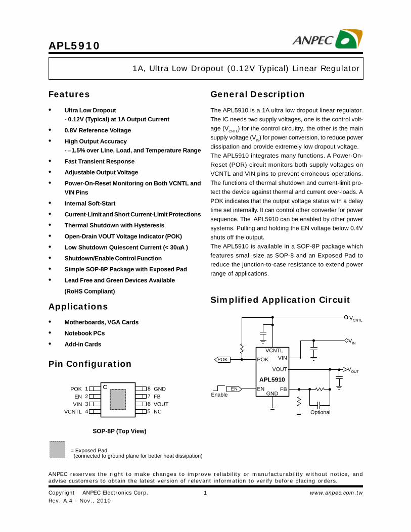
The APL5910 is a 1A ultra low dropout linear regulator.The IC needs two supply voltages, one is the control volt-age (VCNTL) for the control circuitry, the other is the mainsupply voltage (VIN) for power conversion, to reduce powerdissipation and provide extremely low dropout voltage.The APL5910 integrates many functions. A Power-On-Reset (POR) circuit monitors both supply voltages onVCNTL and VIN pins to prevent erroneous operations.The functions of thermal shutdown and current-limit pro-tect the device against thermal and current over-loads. APOK indicates that the output voltage status with a delaytime set internally. It can control other converter for powersequence. The APL5910 can be enabled by other powersystems. Pulling and holding the EN voltage below 0.4Vshuts off the output.The APL5910 is available in a SOP-8P package whichfeatures small size as SOP-8 and an Exposed Pad toreduce the junction-to-case resistance to extend powerrange of applications.
• Motherboards, VGA Cards
• Notebook PCs
• Add-in Cards
Simplified Application Circuit
Pin Configuration
POKENVIN
VCNTL
1234
GNDFBVOUTNC
8765
SOP-8P (Top View)
= Exposed Pad (connected to ground plane for better heat dissipation)
VCNTL
VOUT
VIN
GND
VOUT
VCNTL
POK VIN
ENEnable
EN
POK
APL5910
FB
Optional

Copyright ANPEC Electronics Corp.Rev. A.4 - Nov., 2010
APL5910
www.anpec.com.tw2
Ordering and Marking Information
Symbol Parameter Rating Unit
VCNTL VCNTL Supply Voltage (VCNTL to GND) -0.3 ~ 6 V
VIN VIN Supply Voltage (VIN to GND) -0.3 ~ 6 V
VOUT VOUT to GND Voltage -0.3 ~ VIN+0.3 V
POK to GND Voltage -0.3 ~ 7 EN, FB to GND Voltage -0.3 ~ VCNTL+0.3 V
PD Power Dissipation 2.5 W
TJ Maximum Junction Temperature 150 οC
TSTG Storage Temperature Range -65 ~ 150 οC
TSDR Maximum Lead Soldering Temperature, 10 Seconds 260 οC
Absolute Maximum Ratings (Note 1)
Thermal CharacteristicsSymbol Parameter Typical Value Unit
θJA Junction-to-Ambient Resistance in Free Air (Note 2)
SOP-8P 50 oC/W
θJC Junction-to-Case Resistance in Free Air (Note 3)
SOP-8P 20 oC/W
Note 2: θJA is measured with the component mounted on a high effective thermal conductivity test board in free air.Note 3: The “Thermal-Pad Temperature” is measured on the PCB copper area connected to the thermal pad of package.
Note: ANPEC lead-free products contain molding compounds/die attach materials and 100% matte tin plate termination finish; whichare fully compliant with RoHS. ANPEC lead-free products meet or exceed the lead-free requirements of IPC/JEDEC J-STD-020D forMSL classification at lead-free peak reflow temperature. ANPEC defines “Green” to mean lead-free (RoHS compliant) and halogenfree (Br or Cl does not exceed 900ppm by weight in homogeneous material and total of Br and Cl does not exceed 1500ppm byweight).
1
2
34
8
7
6
5
Measured PointPCB Copper
APL5910
Handling CodeTemperature RangePackage Code
Package Code KA : SOP-8POperating Ambient Temperature Range I : -40 to 85 oCHandling Code TR : Tape & ReelAssembly Material G : Halogen and Lead Free Device
Assembly Material
APL5910 KA : APL5910XXXXX XXXXX - Date Code
Note 1: Absolute Maximum Ratings are those values beyond which the life of a device may be impaired. Exposure to absolutemaximum rating conditions for extended periods may affect device reliability.

Copyright ANPEC Electronics Corp.Rev. A.4 - Nov., 2010
APL5910
www.anpec.com.tw3
Electrical Characteristics
APL5910 Symbol Parameter Test Conditions
Min. Typ. Max. Unit
SUPPLY CURRENT
IVCNTL VCNTL Supply Current EN=VCNTL, IOUT=0A - 1.0 1.5 mA
ISD VCNTL Supply Current at Shutdown
EN=GND - 20 30 µA
VIN Supply Current at Shutdown
EN=GND, VIN=5.5V - - 1 µA
POWER-ON-RESET (POR)
Rising VCNTL POR Threshold 2.5 2.7 2.9 V
VCNTL POR Hysteresis - 0.4 - V
Rising VIN POR Threshold 0.8 0.9 1.0
VIN POR Hysteresis - 0.5 - V
OUTPUT VOLTAGE
VREF Reference Voltage FB=VOUT, IOUT=10mA,TJ=25oC 0.792 0.8 0.808 V
Output Voltage Accuracy IOUT= 0~1A, TJ= -40~125 oC -1.5 - +1.5 %
Load Regulation IOUT=0A ~1A - 0.06 0.15 %
Line Regulation IOUT=10mA, VCNTL= 3.0 ~ 5.5V -0.15 - +0.15 %/V
VOUT Pull-Low Resistance VCNTL=3.3V,VEN=0V, VOUT<0.8V - 85 - Ω
FB Input Current VFB=0.8V -100 - 100 nA
DROPOUT VOLTAGES
TJ=25oC - 0.13 0.16 VOUT=2.5V
TJ=-40~125oC - - 0.22
TJ=25oC - 0.12 0.15 VOUT=1.8V
TJ=-40~125oC - - 0.20
TJ=25oC - 0.12 0.14
VDROP VIN-to-VOUT Dropout Voltage VCNTL=4.5V, IOUT=1A
VOUT=1.2V TJ=-40~125oC - - 0.19
V
Refer to the typical application circuits. These specifications apply over VCNTL=5V, VIN=1.5V, VOUT=1.2V, andTA= -40 ~ 85oC, unless otherwise specified. Typical values are at TJ=25oC.
Symbol Parameter Range Unit
VCNTL VCNTL Supply Voltage 3.0 ~ 5.5 V
VIN VIN Supply Voltage 1.0 ~ 5.5 V
VOUT VOUT Output Voltage (when VCNTL-VOUT>1.4V) 0.8 ~ VIN - VDROP V
IOUT VOUT Output Current 0 ~ 1 A
R2 FB to GND 1k ~ 24k Ω
IOUT=1A at 25% nominal VOUT 8 ~ 600
IOUT=0.5A at 25% nominal VOUT 8 ~ 900 COUT VOUT Output Capacitance
IOUT=0.25A at 25% nominal VOUT 8 ~ 1100
µF
ESRCOUT ESR of VOUT Output Capacitor 0 ~ 200 mΩ
TA Ambient Temperature -40 ~ 85 οC
TJ Junction Temperature -40 ~ 125 οC
Recommended Operating Conditions
Copyright ANPEC Electronics Corp.Rev. A.4 - Nov., 2010
APL5910
www.anpec.com.tw4
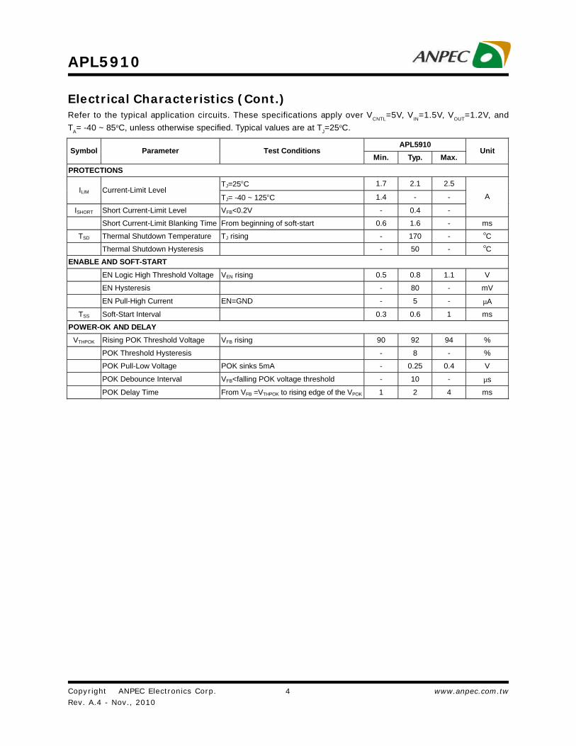
Electrical Characteristics (Cont.)Refer to the typical application circuits. These specifications apply over VCNTL=5V, VIN=1.5V, VOUT=1.2V, andTA= -40 ~ 85oC, unless otherwise specified. Typical values are at TJ=25oC.
APL5910 Symbol Parameter Test Conditions
Min. Typ. Max. Unit
PROTECTIONS
TJ=25οC 1.7 2.1 2.5 ILIM Current-Limit Level
TJ= -40 ~ 125οC 1.4 - -
ISHORT Short Current-Limit Level VFB<0.2V - 0.4 -
A
Short Current-Limit Blanking Time From beginning of soft-start 0.6 1.6 - ms
TSD Thermal Shutdown Temperature TJ rising - 170 - oC
Thermal Shutdown Hysteresis - 50 - oC
ENABLE AND SOFT-START
EN Logic High Threshold Voltage VEN rising 0.5 0.8 1.1 V
EN Hysteresis - 80 - mV
EN Pull-High Current EN=GND - 5 - µA
TSS Soft-Start Interval 0.3 0.6 1 ms
POWER-OK AND DELAY
VTHPOK Rising POK Threshold Voltage VFB rising 90 92 94 %
POK Threshold Hysteresis - 8 - %
POK Pull-Low Voltage POK sinks 5mA - 0.25 0.4 V
POK Debounce Interval VFB<falling POK voltage threshold - 10 - µs
POK Delay Time From VFB =VTHPOK to rising edge of the VPOK 1 2 4 ms
Copyright ANPEC Electronics Corp.Rev. A.4 - Nov., 2010
APL5910
www.anpec.com.tw5
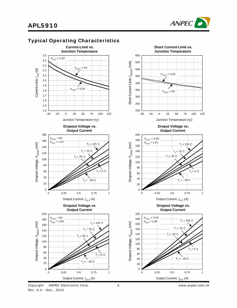
Typical Operating Characteristics
)oC
Cur
rent
-Lim
it, I LI
M (A
)
Junction Temperature (
Current-Limit vs.Junction Temperature
VCNTL = 3.3V
-50 -25 0 25 50 75 100 125
VOUT = 1.2V
VCNTL = 5V
1.4
1.5
1.6
1.7
1.8
1.9
2.0
2.1
2.2
2.3
2.4
2.5
Sho
rt C
urre
nt-L
imit,
I SH
OR
T (m
A)
Junction Temperature ( )oC
Short Current-Limit vs.Junction Temperature
200
250
300
350
400
450
500
550
600
-50 -25 0 25 50 75 100 125
VCNTL = 5V
VCNTL = 3.3V
Dro
pout
Vol
tage
, VD
RO
P (m
V)
Output Current, IOUT (A)
Dropout Voltage vs.Output Current
0 0.25 0.5 0.75 1
VCNTL = 5VVOUT = 1.2V
TJ = 25°C
TJ = 0°C
TJ = 75°C
TJ = 125°C
TJ = - 40°C
0
20
40
60
80
100
120
140
160
180
TJ = 25°C
TJ = 0°C
TJ = 75°C
TJ = 125°C
TJ = - 40°CDro
pout
Vol
tage
, VD
RO
P (m
V)
Output Current, IOUT (A)
Droput Voltage vs.Output Current
0 0.25 0.5 0.75 10
20
40
60
80
100
120
140
160
180
200VCNTL = 3.3VVOUT = 1.2V
200
Dropout Voltage vs.Output Current
Dro
pout
Vol
tage
, VD
RO
P (m
V)
Output Current, IOUT (A)
0
20
40
60
80
100
120
140
160
180
0 0.25 0.5 0.75 1
TJ = 25°C
TJ = 0°C
TJ = 75°C
TJ = 125°C
TJ = - 40°C
VCNTL = 5VVOUT = 1.8V
Dro
pout
Vol
tage
, VD
RO
P (m
V)
Output Current, IOUT (A)
Dropout Voltage vs.Output Current
VCNTL = 3.3VVOUT = 1.8V
TJ = 25°C
TJ = 0°C
TJ = 75°C
TJ = 125°C
TJ = - 40°C
0
20
40
60
80
100
120
140
160
180
200
220
0 0.25 0.5 0.75 1
Copyright ANPEC Electronics Corp.Rev. A.4 - Nov., 2010
APL5910
www.anpec.com.tw6
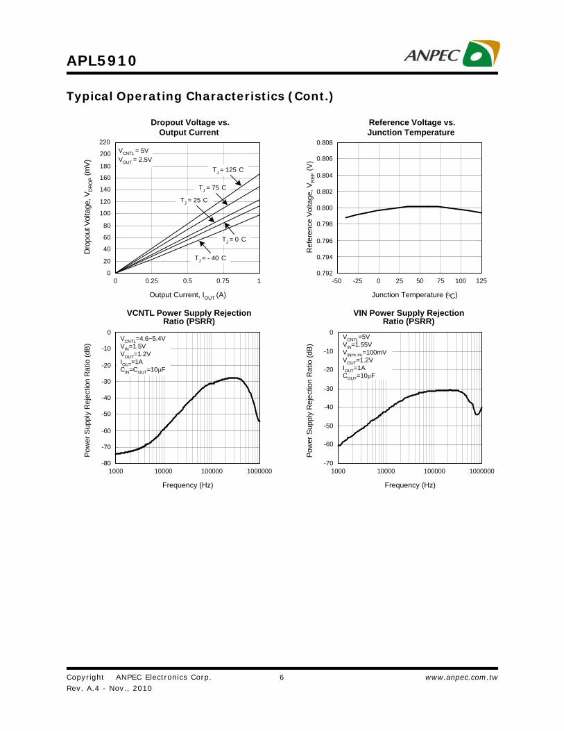
Typical Operating Characteristics (Cont.)D
ropo
ut V
olta
ge, V
DR
OP (m
V)
Output Current, IOUT (A)
Dropout Voltage vs.Output Current
0
20
40
60
80
100
120
140
160
180
200
0 0.25 0.5 0.75 1
VCNTL = 5VVOUT = 2.5V
TJ = 25°C
TJ = 0°C
TJ = 75°C
TJ = 125°C
TJ = - 40°C
220
Junction Temperature ( )oC
Reference Voltage vs.Junction Temperature
-50 -25 0 25 50 75 100
Ref
eren
ce V
olta
ge, V
RE
F (V
)
0.792
0.794
0.796
0.798
0.800
0.802
0.804
0.806
0.808
125
Pow
er S
uppl
y R
ejec
tion
Rat
io (
dB)
Frequency (Hz)
VCNTL Power Supply RejectionRatio (PSRR)
-80
-70
-60
-50
-40
-30
-20
-10
0
1000 10000 100000 1000000
VCNTL=4.6~5.4VVIN=1.5VVOUT=1.2VIOUT=1ACIN=COUT=10µF
Power Supply Rejection Ratio (d
B)
Frequency (Hz)
VIN Power Supply RejectionRatio (PSRR)
-70
-60
-50
-40
-30
-20
-10
0
1000 10000 100000 1000000
VCNTL=5VVIN=1.55VVINPK-PK=100mVVOUT=1.2VIOUT=1ACOUT=10µF
Copyright ANPEC Electronics Corp.Rev. A.4 - Nov., 2010
APL5910
www.anpec.com.tw7
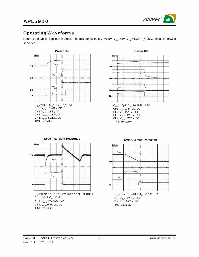
Operating WaveformsRefer to the typical application circuit. The test condition is VIN=1.5V, VCNTL=5V, VOUT=1.2V, TA= 25oC unless otherwisespecified.
Power On
VCNTL1
4
2
3
VIN
VOUT
VPOK
CH1: VCNTL, 5V/Div, DCCH2: VIN, 1V/Div, DC
TIME: 5ms/Div
COUT=10µF, CIN=10µF, RL=1.2Ω
CH3: VOUT, 1V/Div, DCCH4: VPOK, 5V/Div, DC
Power Off
1
4
2
3
VCNTL
VIN
VOUT
VPOK
CH1: VCNTL, 5V/Div, DCCH2: VIN, 1V/Div, DC
TIME: 10ms/Div
COUT=10µF, CIN=10µF, RL=1.2Ω
CH3: VOUT, 1V/Div, DCCH4: VPOK, 5V/Div, DC
CH1: VOUT, 20mV/Div, ACCH4: IOUT, 0.5A/Div, DCTIME: 20µs/Div
COUT=10µF, CIN=10µF
Load Transient Response
IOUT
VOUT
1
4
IOUT=10mA to 1A to 10mA (rise / fall time = 1µs)
Over Current Protection
IOUT
VOUT
1
4
CH4: IOUT, 1A/Div, DCTIME: 50µs/Div
CH1: VOUT, 1V/Div, DC
COUT=10µF, CIN=10µF, IOUT=1A to 2.3A
Copyright ANPEC Electronics Corp.Rev. A.4 - Nov., 2010
APL5910
www.anpec.com.tw8
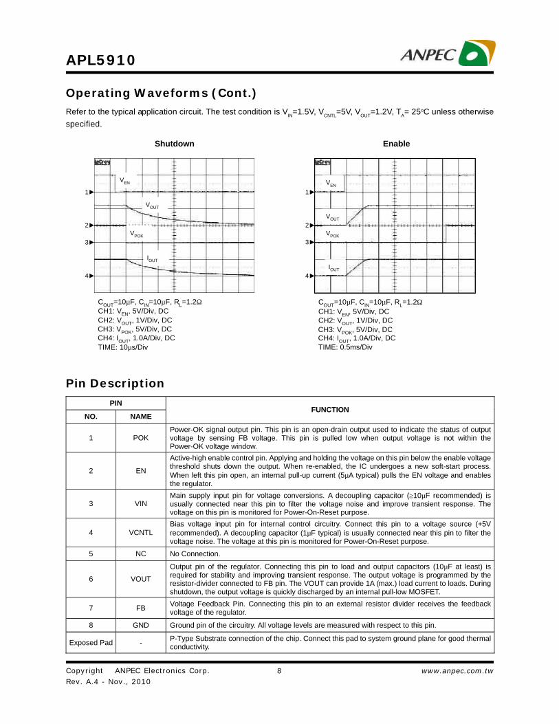
Operating Waveforms (Cont.)Refer to the typical application circuit. The test condition is VIN=1.5V, VCNTL=5V, VOUT=1.2V, TA= 25oC unless otherwisespecified.
CH1: VEN, 5V/Div, DCCH2: VOUT, 1V/Div, DC
TIME: 10µs/Div
COUT=10µF, CIN=10µF, RL=1.2Ω
Shutdown
IOUT
VEN
1
4
2
3
VOUT
VPOK
CH3: VPOK, 5V/Div, DCCH4: IOUT, 1.0A/Div, DC
CH1: VEN, 5V/Div, DCCH2: VOUT, 1V/Div, DC
TIME: 0.5ms/Div
COUT=10µF, CIN=10µF, RL=1.2Ω
Enable
1
4
2
3
IOUT
VEN
VOUT
VPOK
CH3: VPOK, 5V/Div, DCCH4: IOUT, 1.0A/Div, DC
Pin Description
PIN
NO. NAME FUNCTION
1 POK Power-OK signal output pin. This pin is an open-drain output used to indicate the status of output voltage by sensing FB voltage. This pin is pulled low when output voltage is not within the Power-OK voltage window.
2 EN
Active-high enable control pin. Applying and holding the voltage on this pin below the enable voltage threshold shuts down the output. When re-enabled, the IC undergoes a new soft-start process. When left this pin open, an internal pull-up current (5µA typical) pulls the EN voltage and enables the regulator.
3 VIN Main supply input pin for voltage conversions. A decoupling capacitor (≥10µF recommended) is usually connected near this pin to filter the voltage noise and improve transient response. The voltage on this pin is monitored for Power-On-Reset purpose.
4 VCNTL Bias voltage input pin for internal control circuitry. Connect this pin to a voltage source (+5V recommended). A decoupling capacitor (1µF typical) is usually connected near this pin to filter the voltage noise. The voltage at this pin is monitored for Power-On-Reset purpose.
5 NC No Connection.
6 VOUT
Output pin of the regulator. Connecting this pin to load and output capacitors (10µF at least) is required for stability and improving transient response. The output voltage is programmed by the resistor-divider connected to FB pin. The VOUT can provide 1A (max.) load current to loads. During shutdown, the output voltage is quickly discharged by an internal pull-low MOSFET.
7 FB Voltage Feedback Pin. Connecting this pin to an external resistor divider receives the feedback voltage of the regulator.
8 GND Ground pin of the circuitry. All voltage levels are measured with respect to this pin.
Exposed Pad - P-Type Substrate connection of the chip. Connect this pad to system ground plane for good thermal conductivity.

Copyright ANPEC Electronics Corp.Rev. A.4 - Nov., 2010
APL5910
www.anpec.com.tw9
VCNTL
VOUT
CCNTL1µF VIN
GND
VOUT
VCNTL
POK VIN
CIN10µF
COUT10µFEN
EnableEN
POK
R35.1kΩ
3
6
48
2
1
APL5910
R112kΩ
C1Optional
FB7
R224kΩ
(X5R/X7R Recommended)
(X5R/X7R Recommended)
(+5V is preferred)
+1.5V
+1.2V / 1A
Typical Application Circuit
10µF: GRM31MR60J106KE19 Murata
Block Diagram
ThermalShutdown
GND
VOUT
VIN
EN
VCNTL
POK
90%VREF
FB
Delay
0.8V
Control Logicand
Soft-Start
VCNTL
5µA
Enable
POR
POR
ErrorAmplifier
Power-On-Reset
(POR)
PW
OK
Current-Limitand
Short Current-LimitS
oft-Start
Enable
VREF0.8V
ISE
N
Copyright ANPEC Electronics Corp.Rev. A.4 - Nov., 2010
APL5910
www.anpec.com.tw10
Function Description
Power-On-Reset
A Power-On-Reset (POR) circuit monitors both of supplyvoltages on VCNTL and VIN pins to prevent wrong logiccontrols. The POR function initiates a soft-start processafter both of the supply voltages exceed their rising PORvoltage thresholds during powering on. The POR func-tion also pulls low the POK voltage regardless of theoutput status when one of the supply voltages falls belowits falling POR voltage threshold.
Internal Soft-Start
An internal soft-start function controls rise rate of the out-put voltage to limit the current surge during start-up. Thetypical soft-start interval is about 0.6ms.
Output Voltage Regulation
An error amplifier working with a temperature-compen-sated 0.8V reference and an output NMOS regulates out-put to the preset voltage. The error amplifier is designedwith high bandwidth and DC gain provides very fast tran-sient response and less load regulation. It compares thereference with the feedback voltage and amplifies the dif-ference to drive the output NMOS which provides loadcurrent from VIN to VOUT.
Current-Limit Protection
The APL5910 monitors the current flowing through theoutput NMOS and limits the maximum current to preventload and APL5910 from damages during current over-load conditions.
Short Current-Limit Protection
The short current-limit function reduces the current-limitlevel down to 0.4A (typical) when the voltage on FB pinfalls below 0.2V (typical) during current overload or short-circuit conditions.The short current-limit function is disabled for success-ful start-up during soft-start interval.
Thermal Shutdown
A thermal shutdown circuit limits the junction tempera-ture of APL5910. When the junction temperature exceeds+170oC, a thermal sensor turns off the output NMOS, al-lowing the device to cool down. The regulator regulates
Enable Control
The APL5910 has a dedicated enable pin (EN). A logiclow signal applied to this pin shuts down the output. Fol-lowing a shutdown, a logic high signal re-enables theoutput through initiation of a new soft-start cycle. Whenleft open, this pin is pulled up by an internal current source(5µA typical) to enable normal operation. It’s not neces-sary to use an external transistor to save cost.
Power-OK and Delay
The APL5910 indicates the status of the output voltage bymonitoring the feedback voltage (VFB) on FB pin. As theVFB rises and reaches the rising Power-OK voltage thresh-old (VTHPOK), an internal delay function starts to work. At theend of the delay time, the IC turns off the internal NMOS ofthe POK to indicate that the output is ok. As the VFB fallsand reaches the falling Power-OK voltage threshold, theIC turns on the NMOS of the POK (after a debounce time
of 10µs typical).
the output again through initiation of a new soft-start pro-cess after the junction temperature cools by 50oC, result-ing in a pulsed output during continuous thermal over-load conditions. The thermal shutdown is designed witha 50oC hysteresis to lower the average junction tempera-ture during continuous thermal overload conditions, ex-tending lifetime of the device.For normal operation, the device power dissipation shouldbe externally limited so that junction temperatures willnot exceed +125οC.
Copyright ANPEC Electronics Corp.Rev. A.4 - Nov., 2010
APL5910
www.anpec.com.tw11
Application Information
........... (V)
Power Sequencing
The power sequencing of VIN and VCNTL is not neces-sary to be concerned. However, do not apply a voltage toVOUT for a long time when the main voltage applied atVIN does not present. The reason is the internal parasiticdiode from VOUT to VIN conducts and dissipates powerwithout protections due to the forward-voltage.
Output Capacitor
The APL5910 requires a proper output capacitor to main-tain stability and improve transient response. The outputcapacitor selection is dependent upon ESR (equivalentseries resistance) and capacitance of the output capacitorover the operating temperature.
Ultra-low-ESR capacitors (such as ceramic chipcapacitors) and low-ESR bulk capacitors (such as solidtantalum, POSCap, and Aluminum electrolytic capacitors)can all be used as output capacitors.
During load transients, the output capacitors which is de-pending on the stepping amplitude and slew rate of loadcurrent, are used to reduce the slew rate of the currentseen by the APL5910 and help the device to minimize thevariations of output voltage for good transient response.For the applications with large stepping load current, thelow-ESR bulk capacitors are normally recommended.Decoupling ceramic capacitors must be placed at the loadand ground pins as close as possible and the imped-ance of the layout must be minimized.
Input Capacitor
The APL5910 requires proper input capacitors to supplycurrent surge during stepping load transients to preventthe input voltage rail from dropping. Because the para-sitic inductor from the voltage sources or other bulk ca-pacitors to the VIN pin limits the slew rate of the surgecurrents, more parasitic inductance needs, more inputcapacitance.Ultra-low-ESR capacitors (such as ceramic chipcapacitors) and low-ESR bulk capacitors (such as solidtantalum, POSCap, and Aluminum electrolytic capacitors)
can all be used as an input capacitor of VIN. For mostapplications, the recommended input capacitance of VINis 10µF at least. However, if the drop of the input voltageis not cared, the input capacitance can be less than 10µF.
Setting The Output Voltage
The output voltage is programmed by the resistor dividerconnected to FB pin. The preset output voltage is calcu-lated by the following equation :
+⋅=
R2R1
10.8 VOUT
where R1 is the resistor connected from VOUT to FB withKelvin sensing connection and R2 is the resistor con-nected from FB to GND. A bypass capacitor (C1) may beconnected with R1 in parallel to improve load transientresponse and stability.
More capacitance reduces the variations of the supplyvoltage on VIN pin.
Copyright ANPEC Electronics Corp.Rev. A.4 - Nov., 2010
APL5910
www.anpec.com.tw12
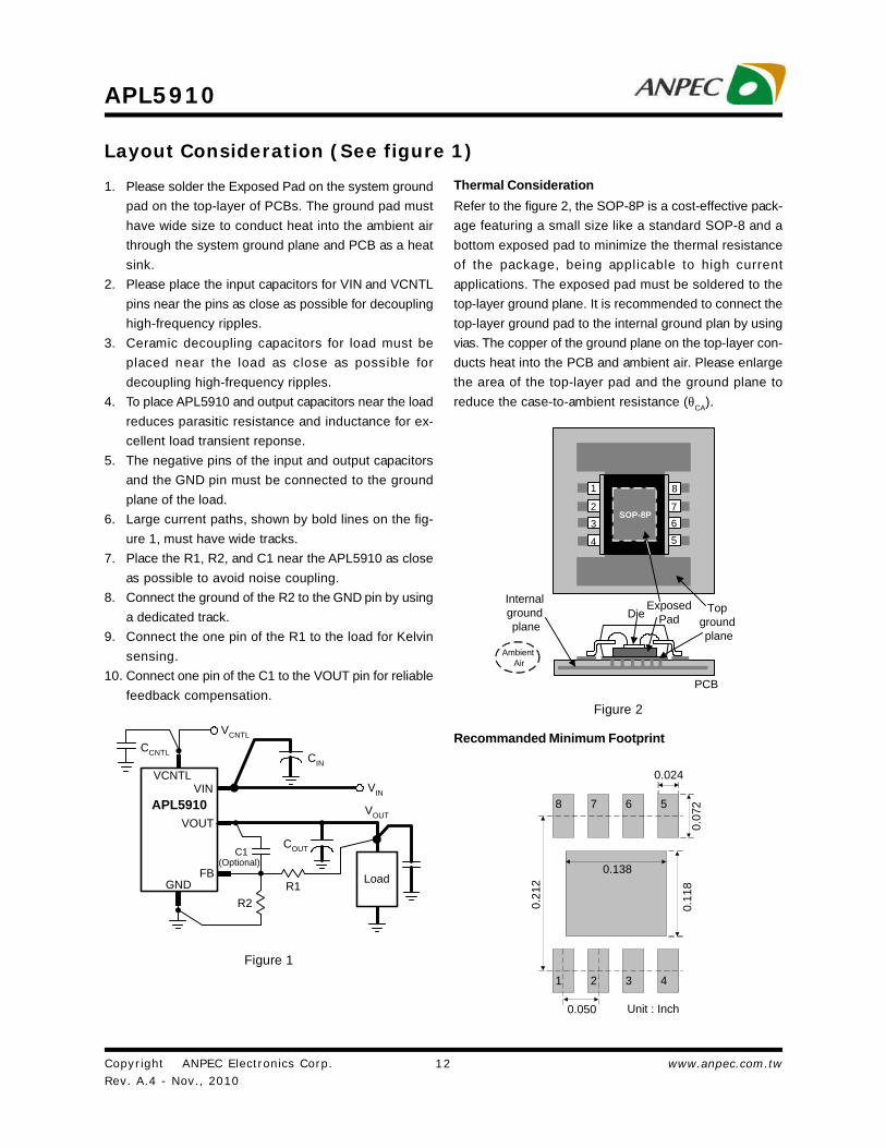
Layout Consideration (See figure 1)
Figure 2
1. Please solder the Exposed Pad on the system groundpad on the top-layer of PCBs. The ground pad musthave wide size to conduct heat into the ambient airthrough the system ground plane and PCB as a heatsink.
2. Please place the input capacitors for VIN and VCNTLpins near the pins as close as possible for decouplinghigh-frequency ripples.
3. Ceramic decoupling capacitors for load must beplaced near the load as close as possible fordecoupling high-frequency ripples.
4. To place APL5910 and output capacitors near the loadreduces parasitic resistance and inductance for ex-cellent load transient reponse.
5. The negative pins of the input and output capacitorsand the GND pin must be connected to the groundplane of the load.
6. Large current paths, shown by bold lines on the fig-ure 1, must have wide tracks.
7. Place the R1, R2, and C1 near the APL5910 as closeas possible to avoid noise coupling.
8. Connect the ground of the R2 to the GND pin by usinga dedicated track.
9. Connect the one pin of the R1 to the load for Kelvinsensing.
10. Connect one pin of the C1 to the VOUT pin for reliablefeedback compensation.
Figure 1
Thermal Consideration
Refer to the figure 2, the SOP-8P is a cost-effective pack-age featuring a small size like a standard SOP-8 and abottom exposed pad to minimize the thermal resistanceof the package, being applicable to high currentapplications. The exposed pad must be soldered to thetop-layer ground plane. It is recommended to connect thetop-layer ground pad to the internal ground plan by usingvias. The copper of the ground plane on the top-layer con-ducts heat into the PCB and ambient air. Please enlargethe area of the top-layer pad and the ground plane toreduce the case-to-ambient resistance (θCA).
Recommanded Minimum Footprint
0.21
2
0.07
2
0.050
0.024
1 2 3 4
8 7 6 5
0.11
8
0.138
Unit : Inch
VCNTL
VOUT
CCNTL
VIN
GND
VOUT
VCNTLVIN
CIN
COUT
APL5910
R1
C1
FB
R2
Load(Optional)
ExposedPadDie Top
ground plane
PCB
Ambient Air
SOP-8P
5
6
7
81
2
3
4
Internalground plane
Copyright ANPEC Electronics Corp.Rev. A.4 - Nov., 2010
APL5910
www.anpec.com.tw13
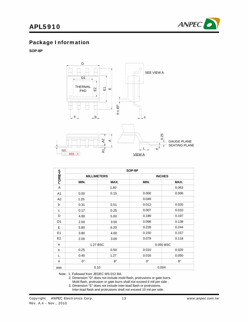
Package InformationSOP-8P
Note : 1. Followed from JEDEC MS-012 BA. 2. Dimension "D" does not include mold flash, protrusions or gate burrs. Mold flash, protrusion or gate burrs shall not exceed 6 mil per side . 3. Dimension "E" does not include inter-lead flash or protrusions. Inter-lead flash and protrusions shall not exceed 10 mil per side.
be
EE1
E2
D
D1
THERMALPAD
SEE VIEW A
ch
x 45
o
A2 A
A1NX
aaa c
GAUGE PLANESEATING PLANE
0.25
L
VIEW Aθ
0.020
0.010
0.020
0.050
0.006
0.063
MAX.
0.40L
0°
E
e
h
E1
0.25
D
c
b
0.17
0.31
0.0161.27
8° 0° 8°
0.50
1.27 BSC
0.51
0.25
0.050 BSC
0.010
0.012
0.007
MILLIMETERS
MIN.
SYMBOL
A1
A2
A
0.00
1.25
SOP-8P
MAX.
0.15
1.60
MIN.
0.000
0.049
INCHES
D1 2.50 0.098
2.00 0.079E2
3.50
3.00
0.138
0.118
4.80 5.00 0.189 0.197
3.80 4.00 0.150 0.157
5.80 6.20 0.228 0.244
0.0040.10
θ
aaa
Copyright ANPEC Electronics Corp.Rev. A.4 - Nov., 2010
APL5910
www.anpec.com.tw14
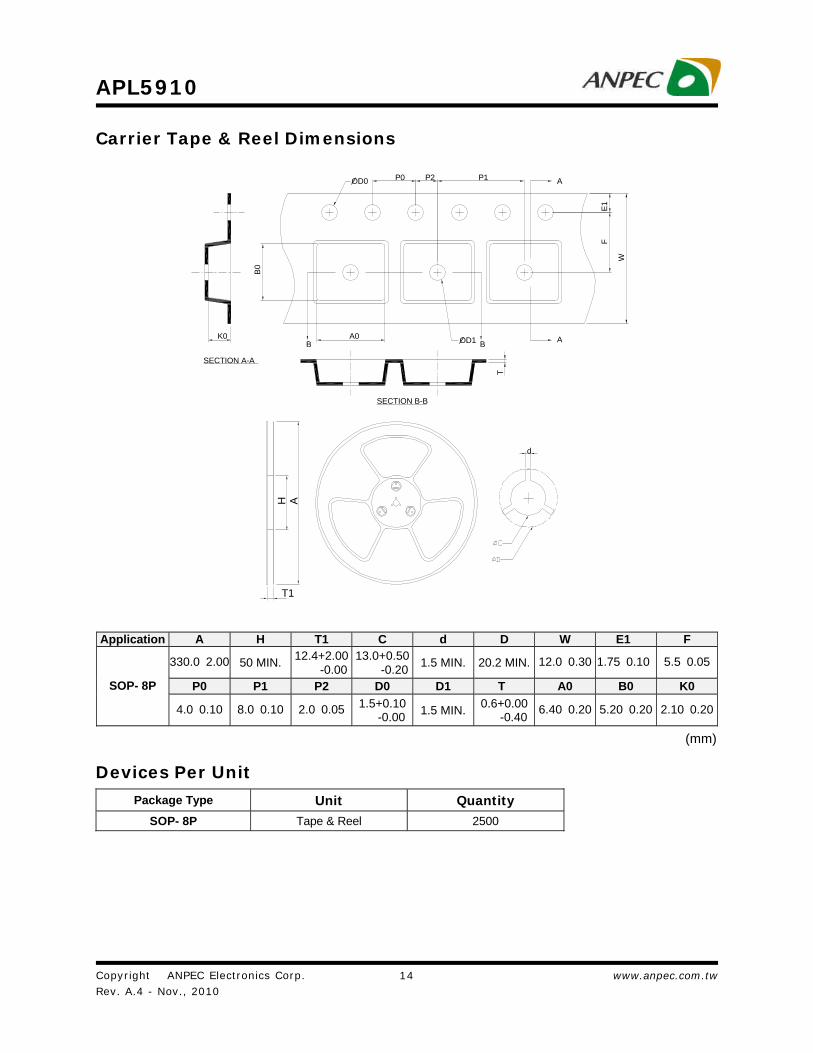
Carrier Tape & Reel Dimensions
Package Type Unit Quantity
SOP- 8P Tape & Reel 2500
Devices Per Unit
Application A H T1 C d D W E1 F
330.0±2.00 50 MIN. 12.4+2.00 -0.00
13.0+0.50 -0.20
1.5 MIN. 20.2 MIN. 12.0±0.30 1.75±0.10 5.5±0.05
P0 P1 P2 D0 D1 T A0 B0 K0 SOP- 8P
4.0±0.10 8.0±0.10 2.0±0.05 1.5+0.10 -0.00 1.5 MIN. 0.6+0.00
-0.40 6.40±0.20 5.20±0.20 2.10±0.20
(mm)
A
E1
AB
W
F
T
P0OD0
BA0
P2
K0
B0
SECTION B-B
SECTION A-A
OD1
P1
H
T1
A
d
Copyright ANPEC Electronics Corp.Rev. A.4 - Nov., 2010
APL5910
www.anpec.com.tw15
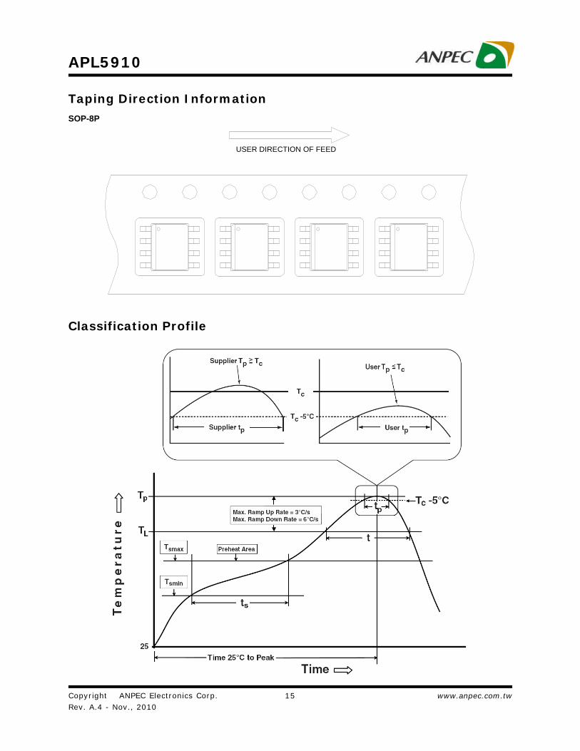
Taping Direction InformationSOP-8P
USER DIRECTION OF FEED
Classification Profile
Copyright ANPEC Electronics Corp.Rev. A.4 - Nov., 2010
APL5910
www.anpec.com.tw16
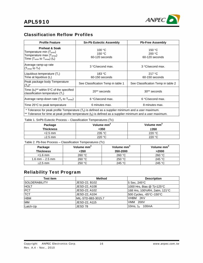
Classification Reflow Profiles
Profile Feature Sn-Pb Eutectic Assembly Pb-Free Assembly
Preheat & Soak Temperature min (Tsmin) Temperature max (Tsmax) Time (Tsmin to Tsmax) (ts)
100 °C 150 °C
60-120 seconds
150 °C 200 °C
60-120 seconds
Average ramp-up rate (Tsmax to TP) 3 °C/second max. 3 °C/second max.
Liquidous temperature (TL) Time at liquidous (tL)
183 °C 60-150 seconds
217 °C 60-150 seconds
Peak package body Temperature (Tp)*
See Classification Temp in table 1 See Classification Temp in table 2
Time (tP)** within 5°C of the specified classification temperature (Tc)
20** seconds 30** seconds
Average ramp-down rate (Tp to Tsmax) 6 °C/second max. 6 °C/second max.
Time 25°C to peak temperature 6 minutes max. 8 minutes max.
* Tolerance for peak profile Temperature (Tp) is defined as a supplier minimum and a user maximum. ** Tolerance for time at peak profile temperature (tp) is defined as a supplier minimum and a user maximum.
Table 2. Pb-free Process – Classification Temperatures (Tc)
Package Thickness
Volume mm3 <350
Volume mm3 350-2000
Volume mm3 >2000
<1.6 mm 260 °C 260 °C 260 °C 1.6 mm – 2.5 mm 260 °C 250 °C 245 °C
≥2.5 mm 250 °C 245 °C 245 °C
Table 1. SnPb Eutectic Process – Classification Temperatures (Tc)
Package Thickness
Volume mm3
<350 Volume mm3
≥350 <2.5 mm 235 °C 220 °C ≥2.5 mm 220 °C 220 °C
Test item Method Description SOLDERABILITY JESD-22, B102 5 Sec, 245°C HOLT JESD-22, A108 1000 Hrs, Bias @ Tj=125°C PCT JESD-22, A102 168 Hrs, 100%RH, 2atm, 121°C TCT JESD-22, A104 500 Cycles, -65°C~150°C HBM MIL-STD-883-3015.7 VHBM≧2KV MM JESD-22, A115 VMM≧200V Latch-Up JESD 78 10ms, 1tr≧100mA
Reliability Test Program
Copyright ANPEC Electronics Corp.Rev. A.4 - Nov., 2010
APL5910
www.anpec.com.tw17
Customer Service
Anpec Electronics Corp.Head Office :
No.6, Dusing 1st Road, SBIP,Hsin-Chu, Taiwan, R.O.C.Tel : 886-3-5642000Fax : 886-3-5642050
Taipei Branch :2F, No. 11, Lane 218, Sec 2 Jhongsing Rd.,Sindian City, Taipei County 23146, TaiwanTel : 886-2-2910-3838Fax : 886-2-2917-3838