a real time power monitoring system - fes final year project
TRANSCRIPT
A REAL TIME POWER MONITORING SYSTEM
HENG FOOK LIANG
A project report submitted in partial fulfilment of the
requirements for the award of the degree of
Bachelor (Hons.) of Electronics and Communications Engineering
Faculty of Engineering and Science
Universiti Tunku Abdul Rahman
May 2011

ii
DECLARATION
I hereby declare that this project report is based on my original work except for
citations and quotations which have been duly acknowledged. I also declare that it
has not been previously and concurrently submitted for any other degree or award at
UTAR or other institutions.
Signature : _________________________
Name : _________________________
ID No. : _________________________
Date : _________________________

iii
APPROVAL FOR SUBMISSION
I certify that this project report entitled “A REAL TIME POWER MONITORING
SYSTEM” was prepared by HENG FOOK LIANG has met the required standard
for submission in partial fulfilment of the requirements for the award of Bachelor
(Hons.) of Electronics and Communications Engineering at Universiti Tunku Abdul
Rahman.
Approved by,
Signature : _________________________
Supervisor : Dr. Lew Kim Luong
Date : _________________________
iv
The copyright of this report belongs to the author under the terms of the
copyright Act 1987 as qualified by Intellectual Property Policy of University Tunku
Abdul Rahman. Due acknowledgement shall always be made of the use of any
material contained in, or derived from, this report.
© 2010, Heng Fook Liang. All right reserved.

v
Specially dedicated to
my beloved grandmother, mother and father

vi
ACKNOWLEDGEMENTS
I would like to thank everyone who had contributed to the successful completion of
this project. I would like to express my gratitude to my research supervisor, Dr. Lew
Kim Luong for his invaluable advice, guidance and his enormous patience
throughout the development of the research.
In addition, I would also like to express my gratitude to my loving parent and
friends who had helped and given me encouragement in this project.
vii
A REAL TIME POWER MONITORING SYSTEM
ABSTRACT
Real time power monitoring system relate generally to the field of electric energy
consumption and more specifically to the power meter having embedded intelligence
to decompose occupy current and voltage signals into specific constituent energy
consumption for the home appliances in real time. In order to help consumers
monitor the energy usage of their electrical appliance, a real time power monitoring
system is used to inform consumers about the current/ power consumption of the
individual electrical appliance to avoid energy wastage. There are 6 sub modules in
the system: Current sensor module, voltage regulate module, voltage inverter module,
op-amp amplifier module, Bridge rectifier module and control unit. The current
measured by the current sensor module will be converted into digital signal by
control unit (PIC) using Analogue-to-Digital conversion. Voltage regulate module is
designed to regulated a constant voltage level from 9V battery to 5V which used for
operated the control unit. Voltage inverter module is needed to provide negative DC
which is provided to start up the op-amp for the purpose of stepping up the current
sensor output signal to ensure it is in the sufficient range to power up the Bridge
Rectifier module for AC to DC conversion. Lastly, Control unit will be performing
various functions such as power consumption calculation, providing alert signal and
display total power consumption through the LCD display. Real time powers
monitoring systems is developed and perform in the current measurement range of
3A to 10A which is appropriate operating range of commercial home electrical
appliances.

viii
TABLE OF CONTENTS
DECLARATION ii
APPROVAL FOR SUBMISSION iii
ACKNOWLEDGEMENTS vi
ABSTRACT vii
TABLE OF CONTENTS viii
LIST OF TABLES xii
LIST OF FIGURES xiii
LIST OF SYMBOLS / ABBREVIATIONS xvi
LIST OF APPENDICES xvii
CHAPTER
1 INTRODUCTION 18
1.1 Project Background and Motivation 18
1 18
1.2 Aims and objectives 19
1.3 Project scope and brief description 20
1.4 Problem Statement 21
1.5 Thesis outline 21
2 LITERATURE REVIEW 23
2.1 Background of power monitoring system 23
2.2 The Effectiveness of Power Consumption Feedback System.
25
2.3 Power supply in Malaysia 26

ix
2.3.1 Plug, main voltage and frequency in Malaysia 26
2.4 Current Capacity Status 27
2.5 Steady State Supply Voltage performance in Malaysia 27
2.6 Important Parameters of Power. 28
2.6.1 Real, reactive, and apparent power 28
2.7 Power factor 30
2.8 Methods of Measurement current 32
2.8.1 Sense resistor 33
2.8.2 Current Transformer 34
2.8.3 Hall Effect Sensor 35
2.8.4 Closed loop Hall Effect Sensor 36
2.9 The benefits and drawbacks of the different current sensor
technologies 37
Sense resistor 37
Current Transformer 37
Hall Effect Sensor 37
2.10 Ideal of Analog to digital conversion 38
2.11 The concept of Bridge Rectifier works (conversion between
AC to DC) 39
2.11.1 Peak loss of the rectifier 40
2.11.2 Rectifier Output Smoothing 41
2.12 Ready product in the Market 41
2.12.1 P3 International - P4400 Kill A Watt 42
2.12.2 Brennenstuhl PM230 Electricity Meter 43
2.12.3 Watts up? .Net 44
2.12.4 TED 5004-C 46
2.13 Hardware and component 47
2.13.1 Current Transducer (LTS-25-NP) 47
2.13.2 Current Transformer (MX3B-30/5A) 49
2.13.3 Microcontroller (PIC 16F877A) 50
2.14 Voltage regulator 51
2.14.1 5V Dc voltage regulator (LM7805) 51
2.14.2 LM317 3-Terminal Adjustable Regulator 52
2.15 Bridge Rectifier 52
x
2.16 LM 555 Timer 53
2.17 Operational amplifier (UA741) 54
2.18 LCD Display Module 54
2.19 Software 55
2.19.1 NI Ultiboard 55
2.20 NI Mulitisim 56
2.21 Proteus VSM 57
2.22 MPLAB IDE 58
2.23 CCS C Compiler 59
3 METHODOLOGY 60
3.1 First Prototype System Overview 60
3.2 First Prototype Hardware implementation 61
3.2.1 First Prototype Current sensor module 61
3.2.2 Voltage regulate module 63
3.2.3 First prototype Control Unit overview 64
3.2.4 First prototype schematic 65
3.2.5 First prototype review 65
3.3 Second prototype Hardware implementation 66
3.3.1 Second prototype system overview 66
3.3.2 Second prototype Current Sensor with Bridge
Rectifier Module 67
3.3.3 Second prototype Voltage inverter 68
3.3.4 Second prototype review 68
3.4 Third prototype hardware implementation 69
3.4.1 Third prototype System overview 69
3.4.2 Third prototype Control Unit 70
3.5 Software implementation 71
4.1 Individual Module Hardware Testing 77
4.1.1 Current Sensor Module Testing 77
4.1.2 Op-amp amplifier module and ±9 V voltage inverter
module testing 83
4.1.3 Bridge Rectifier module testing 87

xi
4.2 Combination modules testing 89
4.3 Final Design Testing 91
4.4 Performance and Efficiency 91
5 CONCLUSION 93
5.1 Limitation of the product 93
5.2 Improvement 95
5.3 Conclusion 96
REFERENCES 97
APPENDIX 99
xii
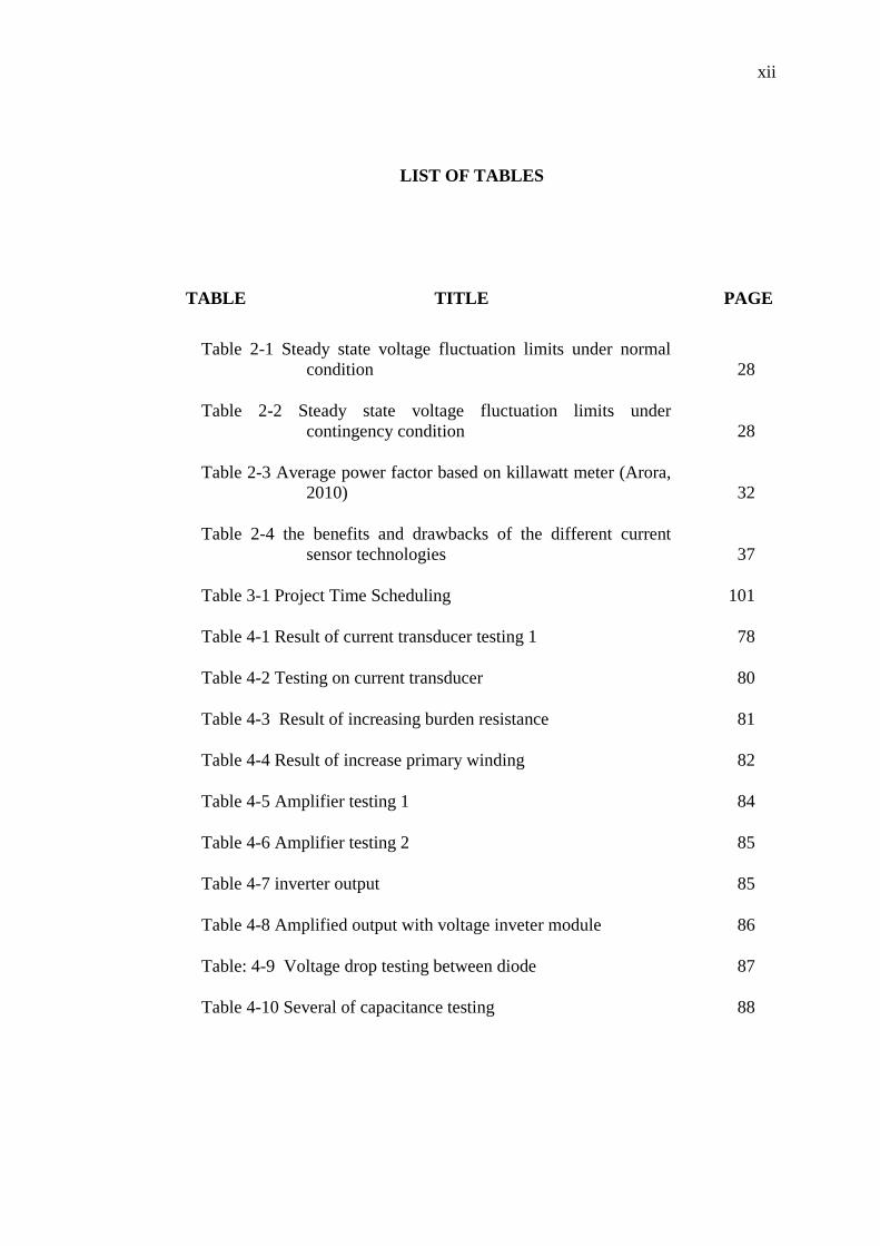
LIST OF TABLES
TABLE TITLE PAGE
Table 2-1 Steady state voltage fluctuation limits under normal
condition 28
Table 2-2 Steady state voltage fluctuation limits under
contingency condition 28
Table 2-3 Average power factor based on killawatt meter (Arora,
2010) 32
Table 2-4 the benefits and drawbacks of the different current
sensor technologies 37
Table 3-1 Project Time Scheduling 101
Table 4-1 Result of current transducer testing 1 78
Table 4-2 Testing on current transducer 80
Table 4-3 Result of increasing burden resistance 81
Table 4-4 Result of increase primary winding 82
Table 4-5 Amplifier testing 1 84
Table 4-6 Amplifier testing 2 85
Table 4-7 inverter output 85
Table 4-8 Amplified output with voltage inveter module 86
Table: 4-9 Voltage drop testing between diode 87
Table 4-10 Several of capacitance testing 88

xiii
LIST OF FIGURES
FIGURE TITLE PAGE
Figure 2-1 Electrical Usage Display System - Patent 4106095 23
Figure 2-2 Apparatus for monitoring and controlling power
consumption 24
Figure 2-3 Plug G and Plug C 26
Figure 2-4 Type-G plug wire distribution 26
Figure 2-5 Current capacity status 27
Figure 2-6 Relation between 3 type of power component 29
Figure 2-7 Voltage to current phase shift 30
Figure 2-8 Current measurement using a shunt resistor and a
differential amplifier 33
Figure 2-9 Current Transformer 34
Figure 2-10 Open loop Hall Effect Sensor 35
Figure 2-11 Closed loop Hall Effect Current Sensor 36
Figure 2-12 The Concept of rectifier 1 39
Figure 2-13 The concept of rectifier 2 40
Figure 2-14 Rectifier smoothing circuit 41
Figure 2-15 P4400 Kill A Watt 42
Figure 2-16 Brennenstuhl PM230 Electricity Meter 43
Figure 2-17 Watts up .Net meter 44
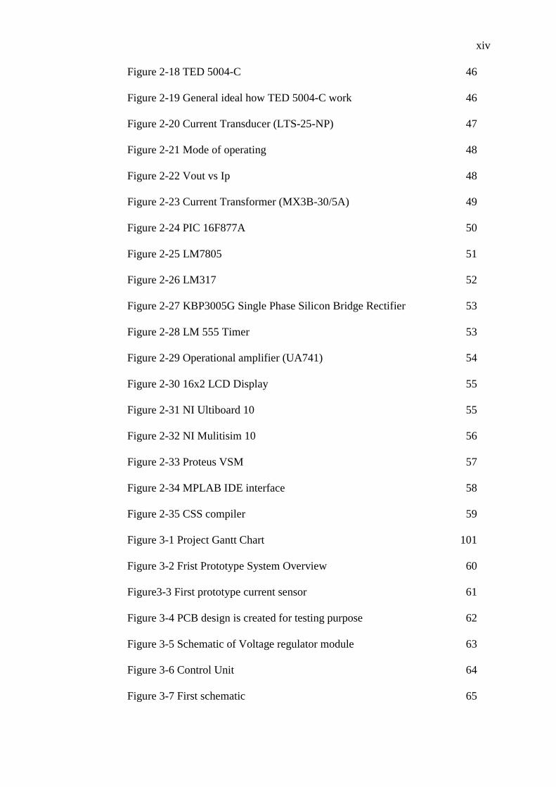
xiv
Figure 2-18 TED 5004-C 46
Figure 2-19 General ideal how TED 5004-C work 46
Figure 2-20 Current Transducer (LTS-25-NP) 47
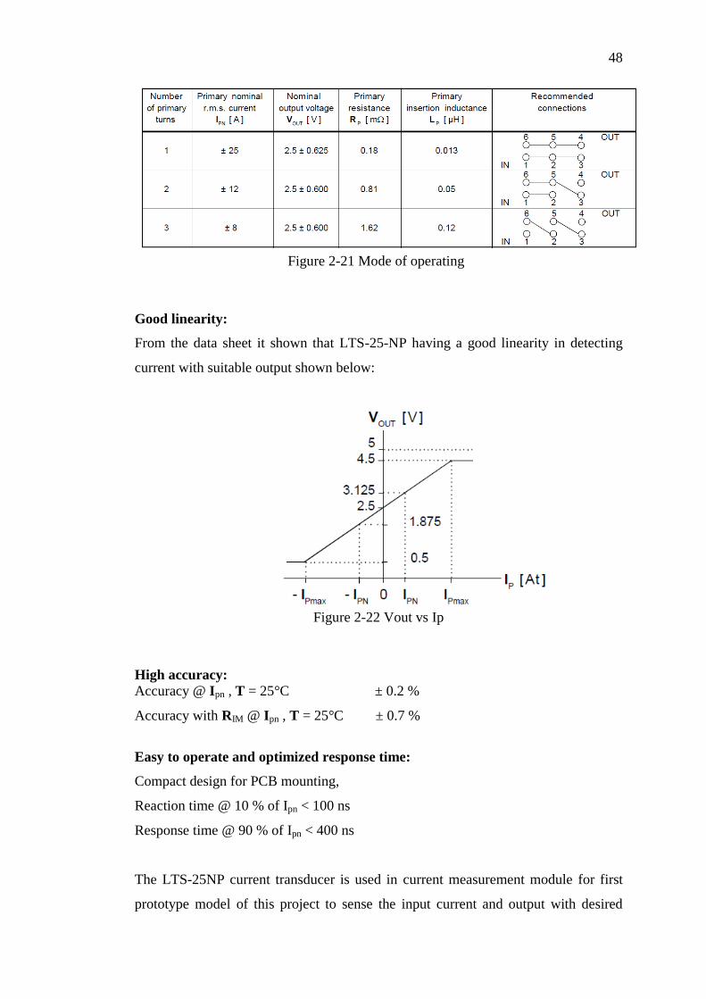
Figure 2-21 Mode of operating 48
Figure 2-22 Vout vs Ip 48
Figure 2-23 Current Transformer (MX3B-30/5A) 49
Figure 2-24 PIC 16F877A 50
Figure 2-25 LM7805 51
Figure 2-26 LM317 52
Figure 2-27 KBP3005G Single Phase Silicon Bridge Rectifier 53
Figure 2-28 LM 555 Timer 53
Figure 2-29 Operational amplifier (UA741) 54
Figure 2-30 16x2 LCD Display 55
Figure 2-31 NI Ultiboard 10 55
Figure 2-32 NI Mulitisim 10 56
Figure 2-33 Proteus VSM 57
Figure 2-34 MPLAB IDE interface 58
Figure 2-35 CSS compiler 59
Figure 3-1 Project Gantt Chart 101
Figure 3-2 Frist Prototype System Overview 60
Figure3-3 First prototype current sensor 61
Figure 3-4 PCB design is created for testing purpose 62
Figure 3-5 Schematic of Voltage regulator module 63
Figure 3-6 Control Unit 64
Figure 3-7 First schematic 65

xv
Figure 3-8 Second prototype system overview 66
Figure 3-9 Current sensor with bridge rectifier design 67
Figure 3-10 Voltage inverter 68
Figure 3-11Third prototype system overview 69
Figure 3-12 PCB design for control unit 70
Figure 3-13 Flow chart of the software design 71
Figure 3-14 Sample Sub Function in the CSS header libraryError! Bookmark not defined.
Figure 4-1 KillaWatt meter 77
Figure 4-2 Primary turn of 2 circuit configuration 78
Figure 4-3 Current transducer testing 1 78
Figure: 4-4 PCB after sparking burn 79
Figure 4-5 Current transducer testing 2 80
Figure4-6 Current transformer testing 81
Figure 4-7 Output waveform for current transformer 83
Figure 4-8 Design of inverting amplifier 83
Figure 4-9 Instrument used in testing op-amp amplifier 84
Figure 4-10 resultant amplified output with DC voltage generator 85
Figure 4-11 op-amp amplifier with ±9V voltage supply 86
Figure 4-12 Bridge rectifier testing 87
Figure: 4-13 P-N junction characteristic 88
Figure 4-14 rectifier output smoothing circuit 88
Figure: 4-15 Resultant DC voltage by using 10 µF capacitance 89
Figure: 4-16 Resultant DC voltage by using 330 µF capacitance 89
Figure 4-17 Combination modules Testing 90
Figure 4-18 Output result of combination modules 90

xvi
LIST OF SYMBOLS / ABBREVIATIONS
LED Light emitting diode
PIC Peripheral Interface Controller
LCD Liquid Crystal Display
PCB Printed circuit board
AC Alternative current
DC Direct current
CFL Compact fluorescent lamp
PF Power Factor
ADC Analog to digital conversion
VAR Volt-amp-reactive
R.M.S Root means square
GND Ground
A Ampere
V Voltage
P Real Power
Q Reactive power
IDE Integrated development environment

xvii
LIST OF APPENDICES
APPENDIX TITLE PAGE
Appendix A User Manual 99
Appendix B Time Schedule 101

18
CHAPTER 1
1 INTRODUCTION
1.1 Project Background and Motivation
1
In last few years, dramatic increases in the price of natural gas and petroleum have
resulted in sharp rise in the cost of electricity for consumer use in Malaysia. Energy
prices have become a major concern for many consumers. Besides that, consumers
also have become increasingly concerned with their impact on the environment.
Using electricity wisely can help you get more value for your electricity bill. It also
helps to conserve natural resources and reduces the impact energy use has on the
environment. Hence, energy efficient appliances have become increasingly popular
with consumers, for example, to lower energy usage expenses associated with the
appliances, as well as reducing an impact on the environment
The consumption habits of modern consumer lifestyles are causing a huge
worldwide waste problem. In a modern home, there are a lot of power consuming
devices and appliances, ranging from toasters and kettles to refrigerator, automatic
washing machines and water heaters. Each device and appliance consumes electrical
power at a different rate and for different lengths of time, with the total power
consumption being recorded by an electricity meter (referred to as the domestic
meter) installed in the home by the utility supplier.
A major disadvantage of domestic meters is that only display the total power
consumption within the home up to the point of inspection. As a consequence the
consumer is not able to monitor the power consumption characteristics of a particular

19
device or appliance or groups of devices of appliances over a prescribed time interval
and cannot access historical power usage statistics for a desired period.
Furthermore, domestic meters are not easy to interpret, firstly they have to be
read, which for modern digital meters can involve cycling through different displays
of measurements until the applicable reading is displayed. This tends not to be a
trivial exercise for the average consumer. The cost of consumed energy is normally
not made available to the user until a monthly statement is received, this delay can be
cause a lot of wastage during periods of high power consumption.
A real time power monitoring system is relates generally to the field of
electric energy consumption and more specifically to the power meter having
embedded intelligence to decompose occupy current and voltage signals into specific
constituent energy consumption for the home appliances in real time. In order to
make energy consumers aware of the energy usage of their various appliances, a real
time power monitoring system help to gain information regarding energy usage is
often provided and alert consumers when it is exceed the current/ power
consumption default set by user (with LED or buzzer). It is hoped that this awareness
will help energy consumers to avoid energy waste in operating their appliances, this
saves electricity and also reduces potential fire hazard. The device is portable it is
possible to track down the appliances that contributed and the consumers can take
action to conserve, by either installing more energy efficient appliances, or changing
their usage behaviours in areas where pricing of electricity varies by time of day, or
simply turning loads off when not in use.
1.2 Aims and objectives
The aim of this final year project is to design and develop a real-time power
monitoring system for household appliances to address the problem of exceed the
power consumption. It should be an accurate and simple to use tool for ordinary
consumers to identify the most energy-greedy appliances, by showing the owner the
total power drain and giving alert when it exceed the power setting. It provides an

20
incentive to track down the excessive background power drain. Thus, he/she can
work out where energy savings can be made.
The objective of this project is
1. To study, learn and research about the background, history, and application of
real time power monitoring system.
2. To study and design an efficient current measurement module and systems.
3. To study and develop a capable hardware/software method to convert analog to
digital signal.
4. To study and write programing statement to PIC microcontroller to perform the
ADC, power consumption calculation, timer, alert signal, LCD display for the
system.
5. To develop a user friendly, portable and efficient real time power monitoring
system.
1.3 Project scope and brief description
This final year project is consists of hardware and software development. This
energy monitor is a processor based unit to monitor electric energy consumption in a
real time basis .At this primitive stage, this project will be developed based on
prototype model. Six parts of modules introduced in the hardware implementation.
There are voltage regulate modules, current sensor module, op-amp amplifier module,
voltage inverter module, Bridge rectifier module and control and display unit. The
software development will be making up with program statement of ADC, power
consumption calculation, LCD display and alert signal. Overview project concept
will be further discussed on chapter 3.
21
1.4 Problem Statement
In order to develop a user friendly, portable and efficient real time power monitoring
system, it required good connection between the main control unit (PIC) and sub
modules. The system becomes inadequate if the sub modules does not report
accurately and timely information. Studied important parameters for power
monitoring, design an efficient current sensor module to provide good data
communication with main control unit module (PIC). Good data interpretation from
AC to DC with performing analog to digital conversion by main control unit module
(PIC). Well organize and design the program statement for circuit control and create
an easy operation interface with LCD display.
1.5 Thesis outline
Chapter 1 is the Introduction of the entire project. In this chapter, the background,
motivations of real time power monitoring system are introduced. Besides, this
chapter also includes the Aims and objectives as well as the project major
applications , problem statement and briefly introduced the overview of the project.
Chapter 2 is the Literature Review of this project. This chapter reviews on the
information plus tools that are useful for developing the projects. The review start
with studying the background of the power monitoring system , The effectiveness
and the Power supply in the Malaysia , I have also do comparison with 3 different
kind of current measurement methods and state out the advantages and drawback.
Hardware, software needed is introduced. Each of these subtopics offers the
fundamental knowledge of the stuffs that used in this project.
Chapter 3 is the Methodology used in this project. It focuses on
implementation work of hardware and software in developing the system. This
chapter mainly explains hardware and software implementation methods, procedures,
and steps.

22
Chapter 4 is the Result and discussion for the project. It emphasize on what the
resultant experimented data on each sub modules , the problem faced in the hardware
and software design , to apply the alternative solution to solved the problem and the
step to making improvements.
Chapter 5 is the Conclusion of the project. In this chapter, it will conclude the overall
of the project and review on the project objectives. It also contains the
recommendation and future works that may be applied for this project for further
improvements.
23
CHAPTER 2
2 LITERATURE REVIEW
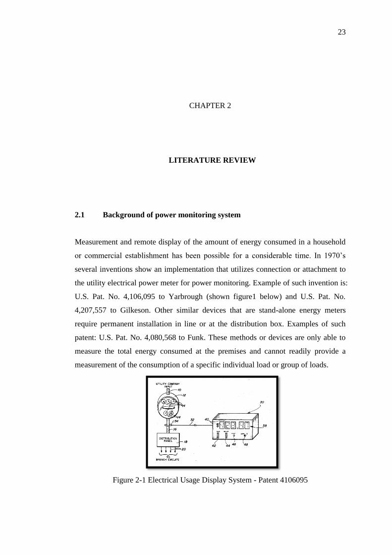
2.1 Background of power monitoring system
Measurement and remote display of the amount of energy consumed in a household
or commercial establishment has been possible for a considerable time. In 1970’s
several inventions show an implementation that utilizes connection or attachment to
the utility electrical power meter for power monitoring. Example of such invention is:
U.S. Pat. No. 4,106,095 to Yarbrough (shown figure1 below) and U.S. Pat. No.
4,207,557 to Gilkeson. Other similar devices that are stand-alone energy meters
require permanent installation in line or at the distribution box. Examples of such
patent: U.S. Pat. No. 4,080,568 to Funk. These methods or devices are only able to
measure the total energy consumed at the premises and cannot readily provide a
measurement of the consumption of a specific individual load or group of loads.
Figure 2-1 Electrical Usage Display System - Patent 4106095
24
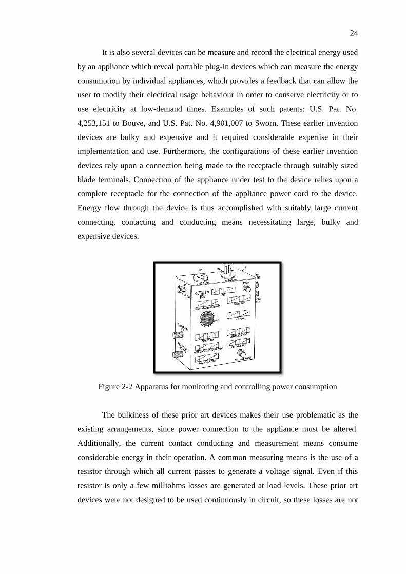
It is also several devices can be measure and record the electrical energy used
by an appliance which reveal portable plug-in devices which can measure the energy
consumption by individual appliances, which provides a feedback that can allow the
user to modify their electrical usage behaviour in order to conserve electricity or to
use electricity at low-demand times. Examples of such patents: U.S. Pat. No.
4,253,151 to Bouve, and U.S. Pat. No. 4,901,007 to Sworn. These earlier invention
devices are bulky and expensive and it required considerable expertise in their
implementation and use. Furthermore, the configurations of these earlier invention
devices rely upon a connection being made to the receptacle through suitably sized
blade terminals. Connection of the appliance under test to the device relies upon a
complete receptacle for the connection of the appliance power cord to the device.
Energy flow through the device is thus accomplished with suitably large current
connecting, contacting and conducting means necessitating large, bulky and
expensive devices.
Figure 2-2 Apparatus for monitoring and controlling power consumption
The bulkiness of these prior art devices makes their use problematic as the
existing arrangements, since power connection to the appliance must be altered.
Additionally, the current contact conducting and measurement means consume
considerable energy in their operation. A common measuring means is the use of a
resistor through which all current passes to generate a voltage signal. Even if this
resistor is only a few milliohms losses are generated at load levels. These prior art
devices were not designed to be used continuously in circuit, so these losses are not

25
substantive in the short term. However, these losses are significant in the long term,
therefore this kind of device are not suitable for long-term monitoring.
Comparing with the present invention, the device now can be used
continuously without substantially altering, smaller size and portable, simple to use
and operational losses through the use of the invention are minimal.
2.2 The Effectiveness of Power Consumption Feedback System.
Metering technologies are as old as the earliest electronic devices, although modern
day meters are far more accurate but it still lack of awareness for consumer to
understand their usage behaviours. For industrial applications, expensive, high-tech
metering solutions are used to minimize costs and to monitor for errors. Most
households, however, still use analog electricity meters attached to the outside of
their homes. These setups provide almost no opportunity for user feedback, except
through monthly billing statements that usually provide little useful data.
Better user feedback has been shown to reduce energy consumption by a
significant amount in many cases. Susan Darby, a researcher at Oxford’s
Environmental Change Institute, has extensively studied energy feedback systems,
and she divides them into five main categories: direct feedback, indirect feedback,
inadvertent feedback, utility controlled feedback, and energy audits. A real power
monitoring device, which is what we have achieved with this project, it is classified
as a direct feedback tool. In a survey of over 38 feedback studies over 25 years,
direct feedback averaged an energy use savings of 10% and faired the best among all
feedback categories (Darby 2001).
Besides that, a study by Ontario Hydro tested direct feedback systems that
consisted of computer monitors with simple data interfaces. The experiment lasted
for a 60-day period with sample and control groups Oehlerking totaling 100
households. The homes with the feedback installed saved an average of 12.9% over
the control groups (Dobson 1992). Since our system also uses LCD to monitors and
display feedback data, we could potentially expect similar results.

26
2.3 Power supply in Malaysia
2.3.1 Plug, main voltage and frequency in Malaysia
The official mains power voltage is AC 230 V .However, the supplied voltage
remains at 240 V except in Penang at 230 V. The socket using in Malaysia is mostly
in type G (BS1363 Fused 13 A, 5 A and 3A .Type C plugs are very common with
audio/video equipment. Plugged into Type G outlets using widely available adapters
or forced in by pushing down the shutter. The latter is widely practiced, although
hazardous.. Type M sockets are normally used for air conditioning (especially if the
air conditioner requires a magnetic starter) and less commonly, washers and clothes
dryers.
Since most of the home appliance are using type G socket with fused 13A, our
design will design based on the plug and the range of current.
Figure 2-3 Plug G and Plug C
Figure below shown Type-G plug wire distribution, consist of 3 cable namely Live
(hot, brown), Neutral (return, blue) and Earth (safety ground, yellow/green).
Figure 2-4 Type-G plug wire distribution

27
2.4 Current Capacity Status
According the report release in TNB website, In June 2010, total available capacity
in Peninsular Malaysia stands at 21,052 MW. The highest number of installed plants
is gas plants. The total current available capacity of this type of plant is 12,205 MW.
Coal plants with 6933 MW of available capacity constitutes to 33% of the capacity
mix. It is then followed by hydro plants which accounts for 9% of capacity mix at
available capacity of 1852 MW. As for distillate plant, current available capacity
stands at 62MW and it contributes to only 0.3% of the mix.
It is apparent that we are highly depended on fossil fuel sources; approximately 90%
of our dependable capacity is either from gas, coal or distillate. As of now, only
hydro is our major non fossil option
Figure 2-5 Current capacity status
2.5 Steady State Supply Voltage performance in Malaysia
The voltage regulation is highly related to applicance power consumption ,since we
need determine the voltage to calculate the power consumption by the device.
Therefore we need to study about the voltage variation for the power supply in
Malaysia. The term “voltage regulation” is used to discuss long term variation in
voltage. It does not included short-term variations , which are generally called
voltage sags or voltage swells.
28
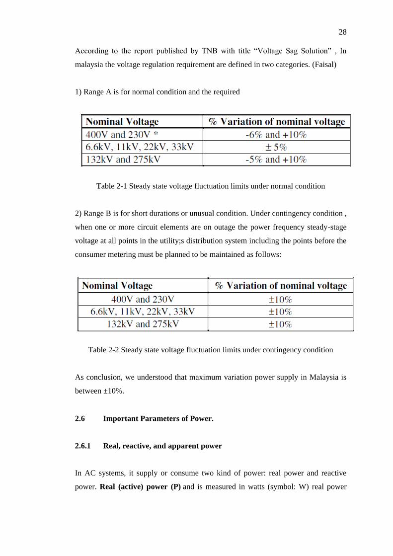
According to the report published by TNB with title “Voltage Sag Solution” , In
malaysia the voltage regulation requirement are defined in two categories. (Faisal)
1) Range A is for normal condition and the required
Table 2-1 Steady state voltage fluctuation limits under normal condition
2) Range B is for short durations or unusual condition. Under contingency condition ,
when one or more circuit elements are on outage the power frequency steady-stage
voltage at all points in the utility;s distribution system including the points before the
consumer metering must be planned to be maintained as follows:
Table 2-2 Steady state voltage fluctuation limits under contingency condition
As conclusion, we understood that maximum variation power supply in Malaysia is
between ±10%.
2.6 Important Parameters of Power.
2.6.1 Real, reactive, and apparent power
In AC systems, it supply or consume two kind of power: real power and reactive
power. Real (active) power (P) and is measured in watts (symbol: W) real power

29
accomplishes useful work It represents that actual work done by an electric current or
an actual energy consumed by a load to create for example heat, light or motion.
Reactive power (Q) is the power consumed in an AC circuit because
of the expansion and collapse of magnetic (inductive) and electrostatic (capacitive)
fields. Reactive power is expressed in volt-amperes-reactive (VAR). Unlike true
power, reactive power is not useful power because it is stored in the circuit itself.
This power is stored by inductors, because they expand and collapse their magnetic
field in an attempt to keep current constant, and by capacitors, because they charge
and discharge in an attempt to keep voltage constant.
Besides that the total power is called the apparent power (S) and measured by volt-
amperes or VA.
Figure below shown the relation between 3 components:
Figure 2-6 Relation between 3 type of power component
In the real time power monitoring system, the load is depending on what appliance
that we measured .For the purely resistive circuit for example incandescent light bulb,
water heater, the power factor is 1 because the reactive power equals to zero. Here,
the power triangle would look like a horizontal line, because the opposite (reactive
power) side would have zero length. Therefore real power will be equal as apparent
power (Systems, 2009).

30
For the purely inductive circuit and capacitive circuit, the power factor is zero,
because true power equals zero. Here, the power triangle would look like a vertical
line, because the adjacent (true power) side would have zero length. Magnetic
(inductive) loads, such as motor in the home appliance will cause reactive power
occurred, it cause draw more VA than actual real power. The extra component is
called a VAR. a VAR (volt-amp-reactive) is basically magnetic power, which causes
a phase shift between voltage and current curves shown as figure below (M. Tavakoli
Bina, 2011):
Figure 2-7 Voltage to current phase shift
2.7 Power factor
The power factor is important parameters in our design ,the power factor of
an AC electric power system is defined as the ratio of the real power flowing to the
load to the apparent power. Electrical equipment with non-resistive load has a power
factor of less than 1. As an example, we know that CFL (compact fluorescent lamp)
light bulbs have a Power factor of between 0.6 ~0.7 depending on maker and wattage.
Power factor can be an important aspect to consider in an AC circuit. From the
equation (1) and (2) we may know if the power factor less than 1 means (inductive
load) that the circuit's wiring has to carry more current than what would be necessary
with zero reactance in the circuit to deliver the same amount of (true) power to the
resistive load as at this time apparent power will be combination of true power and
reactive power.
31
Power factor will not much affect to end consumer, it is because the
electricity meter is based on true power to charge consumer electricity bill, but in our
design we are highly concern about this issues. Hence let look into depth with the
power factor different in the home appliance.
Electric motors, fluorescent lamps, refrigerator, and consumer electronics
(such as televisions and computers) are examples of appliances that have power
factors of less than one. This is because they include some type of storage element
such as a capacitance or inductance. Since energy efficiency is highly concern, in
modern day most of the home appliance is fitted with power factor-corrected power
supplies, the average power factor will be maintain within 0.8 to 0.9 to such devices.
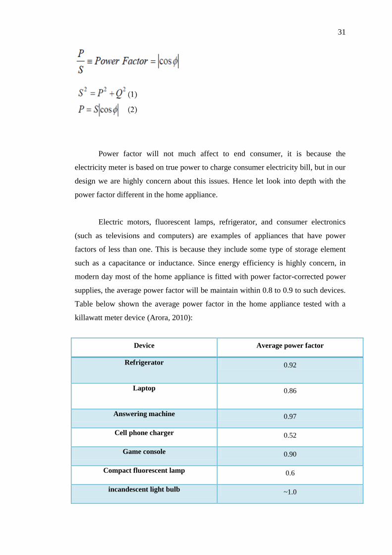
Table below shown the average power factor in the home appliance tested with a
killawatt meter device (Arora, 2010):
Device Average power factor
Refrigerator
0.92
Laptop
0.86
Answering machine 0.97
Cell phone charger 0.52
Game console 0.90
Compact fluorescent lamp 0.6
incandescent light bulb ~1.0
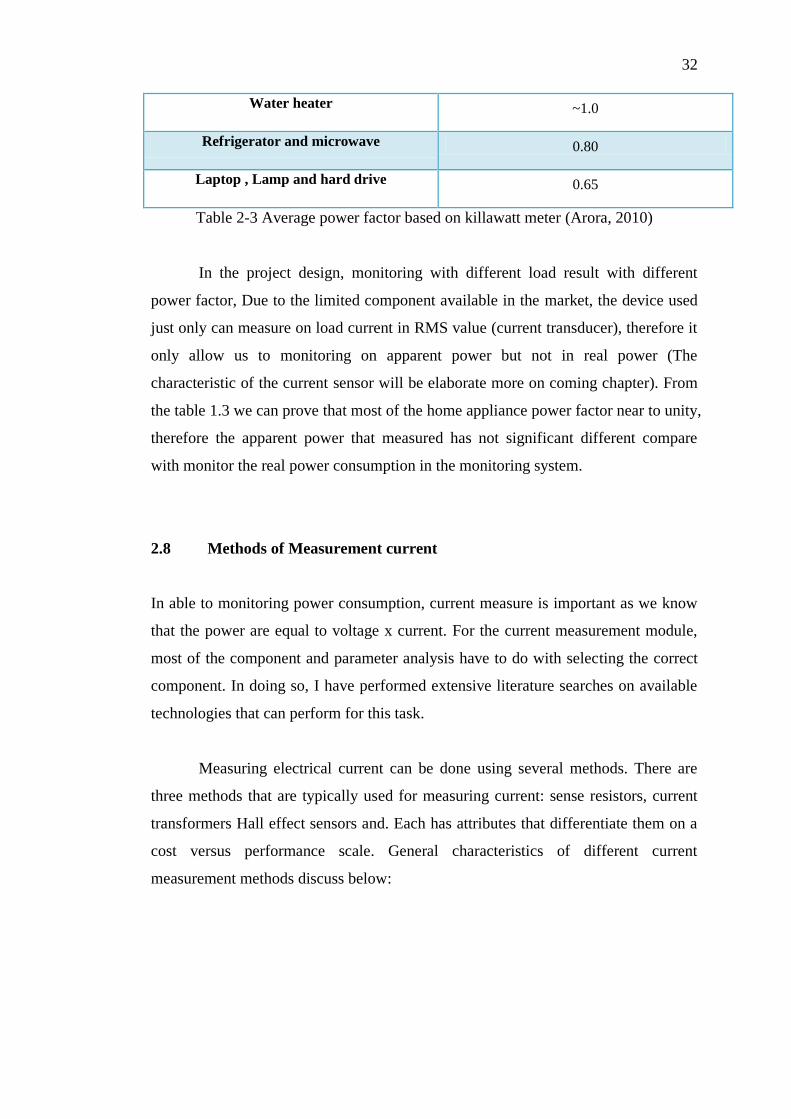
32
Water heater ~1.0
Refrigerator and microwave 0.80
Laptop , Lamp and hard drive 0.65
Table 2-3 Average power factor based on killawatt meter (Arora, 2010)
In the project design, monitoring with different load result with different
power factor, Due to the limited component available in the market, the device used
just only can measure on load current in RMS value (current transducer), therefore it
only allow us to monitoring on apparent power but not in real power (The
characteristic of the current sensor will be elaborate more on coming chapter). From
the table 1.3 we can prove that most of the home appliance power factor near to unity,
therefore the apparent power that measured has not significant different compare
with monitor the real power consumption in the monitoring system.
2.8 Methods of Measurement current
In able to monitoring power consumption, current measure is important as we know
that the power are equal to voltage x current. For the current measurement module,
most of the component and parameter analysis have to do with selecting the correct
component. In doing so, I have performed extensive literature searches on available
technologies that can perform for this task.
Measuring electrical current can be done using several methods. There are
three methods that are typically used for measuring current: sense resistors, current
transformers Hall effect sensors and. Each has attributes that differentiate them on a
cost versus performance scale. General characteristics of different current
measurement methods discuss below:
33
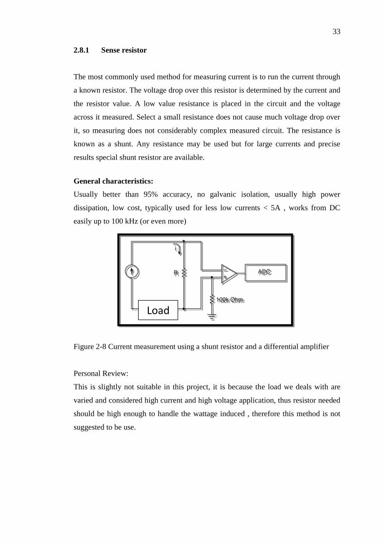
2.8.1 Sense resistor
The most commonly used method for measuring current is to run the current through
a known resistor. The voltage drop over this resistor is determined by the current and
the resistor value. A low value resistance is placed in the circuit and the voltage
across it measured. Select a small resistance does not cause much voltage drop over
it, so measuring does not considerably complex measured circuit. The resistance is
known as a shunt. Any resistance may be used but for large currents and precise
results special shunt resistor are available.
General characteristics:
Usually better than 95% accuracy, no galvanic isolation, usually high power
dissipation, low cost, typically used for less low currents < 5A , works from DC
easily up to 100 kHz (or even more)
Figure 2-8 Current measurement using a shunt resistor and a differential amplifier
Personal Review:
This is slightly not suitable in this project, it is because the load we deals with are
varied and considered high current and high voltage application, thus resistor needed
should be high enough to handle the wattage induced , therefore this method is not
suggested to be use.
Load
34
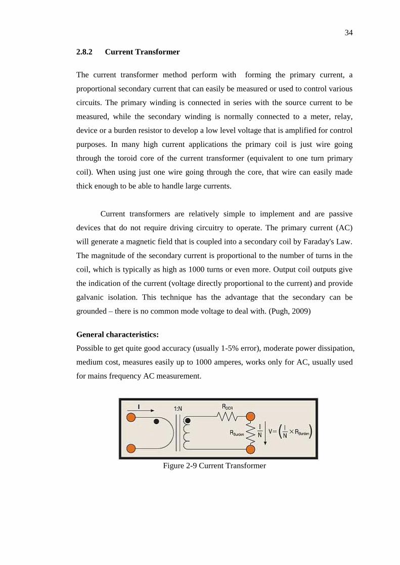
2.8.2 Current Transformer
The current transformer method perform with forming the primary current, a
proportional secondary current that can easily be measured or used to control various
circuits. The primary winding is connected in series with the source current to be
measured, while the secondary winding is normally connected to a meter, relay,
device or a burden resistor to develop a low level voltage that is amplified for control
purposes. In many high current applications the primary coil is just wire going
through the toroid core of the current transformer (equivalent to one turn primary
coil). When using just one wire going through the core, that wire can easily made
thick enough to be able to handle large currents.
Current transformers are relatively simple to implement and are passive
devices that do not require driving circuitry to operate. The primary current (AC)
will generate a magnetic field that is coupled into a secondary coil by Faraday's Law.
The magnitude of the secondary current is proportional to the number of turns in the
coil, which is typically as high as 1000 turns or even more. Output coil outputs give
the indication of the current (voltage directly proportional to the current) and provide
galvanic isolation. This technique has the advantage that the secondary can be
grounded – there is no common mode voltage to deal with. (Pugh, 2009)
General characteristics:
Possible to get quite good accuracy (usually 1-5% error), moderate power dissipation,
medium cost, measures easily up to 1000 amperes, works only for AC, usually used
for mains frequency AC measurement.
Figure 2-9 Current Transformer
35
2.8.3 Hall Effect Sensor
The Hall effect uses a semiconductor sensor to convert the magnetic field
accompanying the measurement current, into a signal voltage. The output includes
both DC and AC components, which makes it attractive. There are two techniques
for sensing current using Hall effect devices, open loop and closed loop. The
working principle discuss as below:
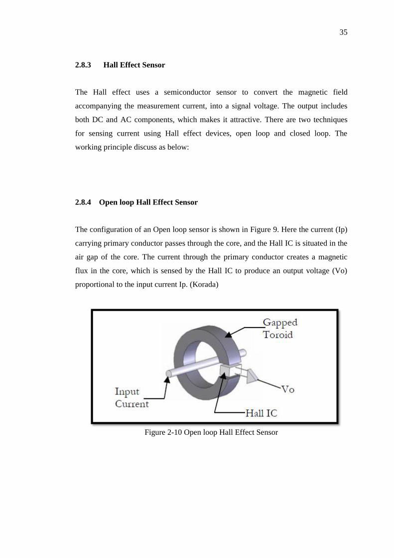
2.8.4 Open loop Hall Effect Sensor
The configuration of an Open loop sensor is shown in Figure 9. Here the current (Ip)
carrying primary conductor passes through the core, and the Hall IC is situated in the
air gap of the core. The current through the primary conductor creates a magnetic
flux in the core, which is sensed by the Hall IC to produce an output voltage (Vo)
proportional to the input current Ip. (Korada)
Figure 2-10 Open loop Hall Effect Sensor
36
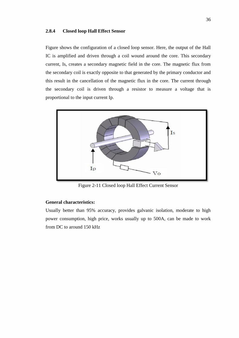
2.8.4 Closed loop Hall Effect Sensor
Figure shows the configuration of a closed loop sensor. Here, the output of the Hall
IC is amplified and driven through a coil wound around the core. This secondary
current, Is, creates a secondary magnetic field in the core. The magnetic flux from
the secondary coil is exactly opposite to that generated by the primary conductor and
this result in the cancellation of the magnetic flux in the core. The current through
the secondary coil is driven through a resistor to measure a voltage that is
proportional to the input current Ip.
Figure 2-11 Closed loop Hall Effect Current Sensor
General characteristics:
Usually better than 95% accuracy, provides galvanic isolation, moderate to high
power consumption, high price, works usually up to 500A, can be made to work
from DC to around 150 kHz
37
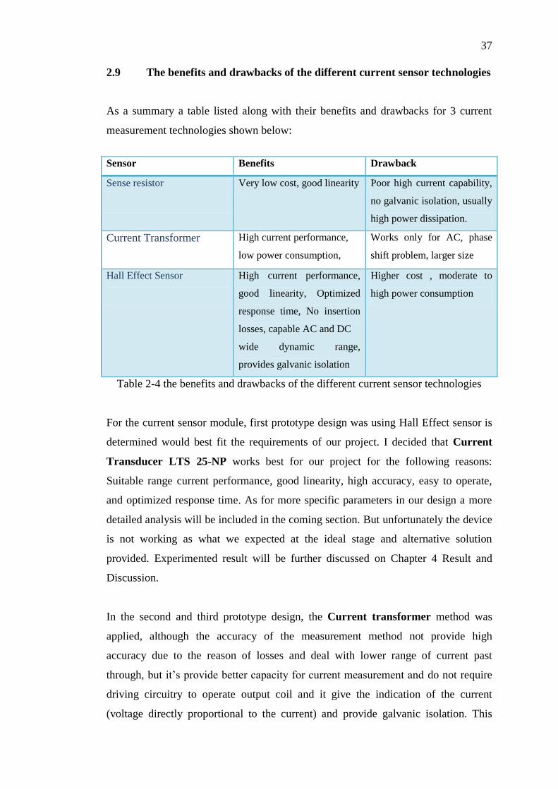
2.9 The benefits and drawbacks of the different current sensor technologies
As a summary a table listed along with their benefits and drawbacks for 3 current
measurement technologies shown below:
Sensor Benefits Drawback
Sense resistor
Very low cost, good linearity Poor high current capability,
no galvanic isolation, usually
high power dissipation.
Current Transformer
High current performance,
low power consumption,
Works only for AC, phase
shift problem, larger size
Hall Effect Sensor
High current performance,
good linearity, Optimized
response time, No insertion
losses, capable AC and DC
wide dynamic range,
provides galvanic isolation
Higher cost , moderate to
high power consumption
Table 2-4 the benefits and drawbacks of the different current sensor technologies
For the current sensor module, first prototype design was using Hall Effect sensor is
determined would best fit the requirements of our project. I decided that Current
Transducer LTS 25-NP works best for our project for the following reasons:
Suitable range current performance, good linearity, high accuracy, easy to operate,
and optimized response time. As for more specific parameters in our design a more
detailed analysis will be included in the coming section. But unfortunately the device
is not working as what we expected at the ideal stage and alternative solution
provided. Experimented result will be further discussed on Chapter 4 Result and
Discussion.
In the second and third prototype design, the Current transformer method was
applied, although the accuracy of the measurement method not provide high
accuracy due to the reason of losses and deal with lower range of current past
through, but it’s provide better capacity for current measurement and do not require
driving circuitry to operate output coil and it give the indication of the current
(voltage directly proportional to the current) and provide galvanic isolation. This
38
technique has the advantage that the secondary can be grounded therefore more
safety compare to the Current transducer which need to feed the current to the
circuitry for current measurement.
2.10 Ideal of Analog to digital conversion
Analog-to-digital conversion is an electronic process in which a continuously
variable (analog) signal is changed, without altering its essential content, into a
multi-level (digital) signal. The input to an analog-to-digital converter
(ADC) consists of a voltage that varies among a theoretically infinite number of
values but in our project is refer to the DC voltage value. The output of the ADC, in
contrast, has defined levels or states.
The resolution of an ADC is usually expressed as the number of bits in its
digital output code. For example, an ADC with an n-bit resolution has 2n possible
digital codes which define 2n step levels. The width of one step is defined as 1 LSB
(one least significant bit) and this is often used as the reference unit for other
quantities in the specification. 1 LSB = VREF / 2n.
Besides that selecting the most
suitable A/D converter (ADC) for your application is based on more than just the
precision or bits. Different architectures are available, each exhibiting advantages
and disadvantages in various data-acquisition systems. The required accuracy or
precision of the system puts you in a category based on the number of bits required.
It is important to always design your system to allow for more bits than initially
required: if an application calls for 10 bits of accuracy, choose a 12-bit converter.
The achievable accuracy of a converter will always be less than the total number of
bits available.
In the project, I would like to perform ADC by using PIC microcontroller
which has a 10 bit resolution within 0-5V input which is suitable for the output from
the current sensor module. Specification of the PIC will be further discussed in the
chapter 2.12 Hardware and component (Morton, The PIC microcontroller: your
personal introductory course, 2005).
39
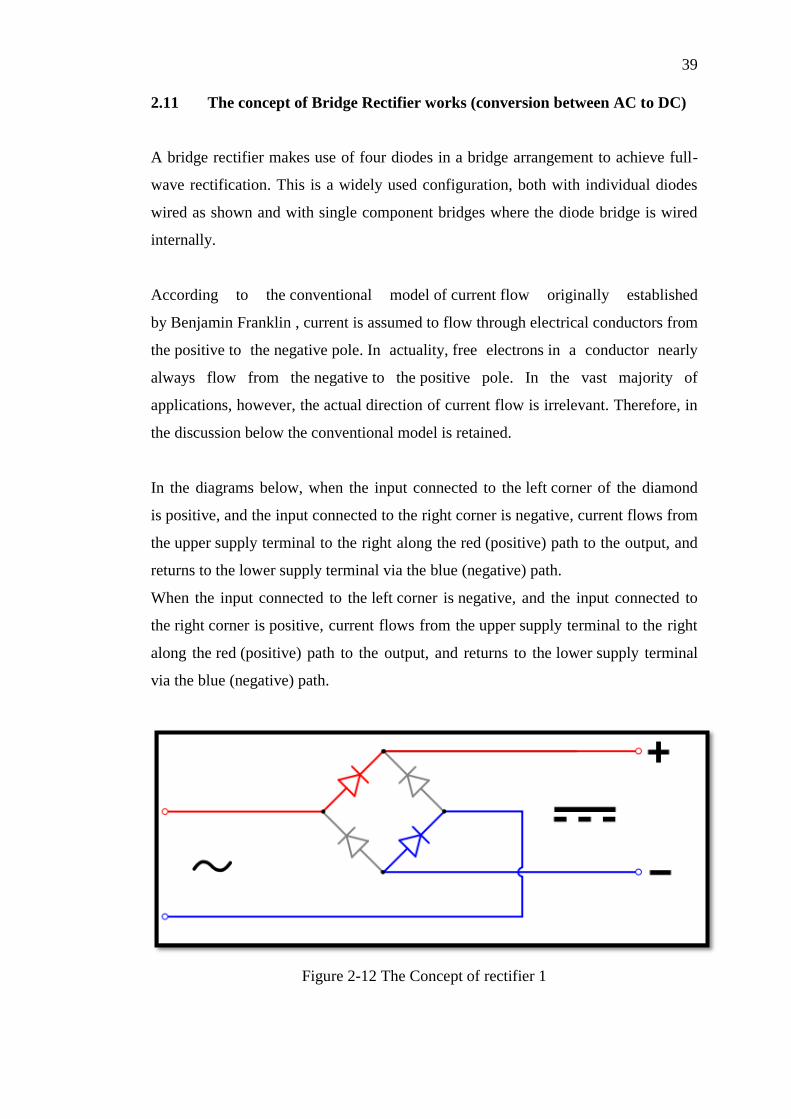
2.11 The concept of Bridge Rectifier works (conversion between AC to DC)
A bridge rectifier makes use of four diodes in a bridge arrangement to achieve full-
wave rectification. This is a widely used configuration, both with individual diodes
wired as shown and with single component bridges where the diode bridge is wired
internally.
According to the conventional model of current flow originally established
by Benjamin Franklin , current is assumed to flow through electrical conductors from
the positive to the negative pole. In actuality, free electrons in a conductor nearly
always flow from the negative to the positive pole. In the vast majority of
applications, however, the actual direction of current flow is irrelevant. Therefore, in
the discussion below the conventional model is retained.
In the diagrams below, when the input connected to the left corner of the diamond
is positive, and the input connected to the right corner is negative, current flows from
the upper supply terminal to the right along the red (positive) path to the output, and
returns to the lower supply terminal via the blue (negative) path.
When the input connected to the left corner is negative, and the input connected to
the right corner is positive, current flows from the upper supply terminal to the right
along the red (positive) path to the output, and returns to the lower supply terminal
via the blue (negative) path.
Figure 2-12 The Concept of rectifier 1
40
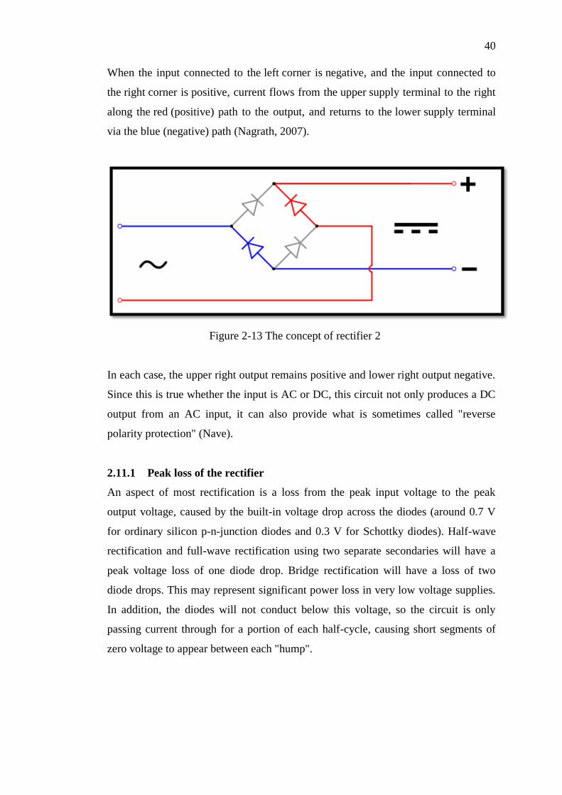
When the input connected to the left corner is negative, and the input connected to
the right corner is positive, current flows from the upper supply terminal to the right
along the red (positive) path to the output, and returns to the lower supply terminal
via the blue (negative) path (Nagrath, 2007).
Figure 2-13 The concept of rectifier 2
In each case, the upper right output remains positive and lower right output negative.
Since this is true whether the input is AC or DC, this circuit not only produces a DC
output from an AC input, it can also provide what is sometimes called "reverse
polarity protection" (Nave).
2.11.1 Peak loss of the rectifier
An aspect of most rectification is a loss from the peak input voltage to the peak
output voltage, caused by the built-in voltage drop across the diodes (around 0.7 V
for ordinary silicon p-n-junction diodes and 0.3 V for Schottky diodes). Half-wave
rectification and full-wave rectification using two separate secondaries will have a
peak voltage loss of one diode drop. Bridge rectification will have a loss of two
diode drops. This may represent significant power loss in very low voltage supplies.
In addition, the diodes will not conduct below this voltage, so the circuit is only
passing current through for a portion of each half-cycle, causing short segments of
zero voltage to appear between each "hump".
41
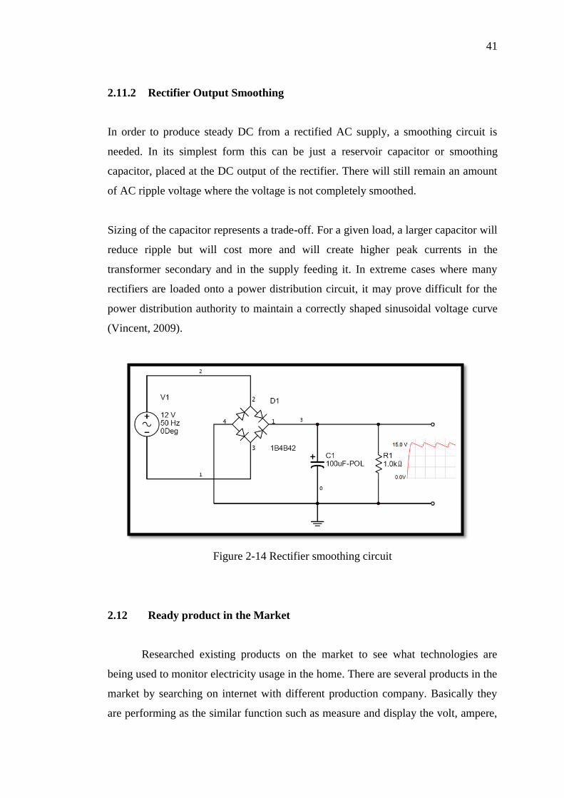
2.11.2 Rectifier Output Smoothing
In order to produce steady DC from a rectified AC supply, a smoothing circuit is
needed. In its simplest form this can be just a reservoir capacitor or smoothing
capacitor, placed at the DC output of the rectifier. There will still remain an amount
of AC ripple voltage where the voltage is not completely smoothed.
Sizing of the capacitor represents a trade-off. For a given load, a larger capacitor will
reduce ripple but will cost more and will create higher peak currents in the
transformer secondary and in the supply feeding it. In extreme cases where many
rectifiers are loaded onto a power distribution circuit, it may prove difficult for the
power distribution authority to maintain a correctly shaped sinusoidal voltage curve
(Vincent, 2009).
Figure 2-14 Rectifier smoothing circuit
2.12 Ready product in the Market
Researched existing products on the market to see what technologies are
being used to monitor electricity usage in the home. There are several products in the
market by searching on internet with different production company. Basically they
are performing as the similar function such as measure and display the volt, ampere,

42
frequency, and kilo-watts-house (KWH). However each of them has different
specification to satisfy the standard in different countries used electrical supply.
These are some examples of the energy monitor product:
2.12.1 P3 International - P4400 Kill A Watt
Figure 2-15 P4400 Kill A Watt
P3 International P4400, as known as Kill-A-Watt meter is one of the most popular
energy monitor device in United States. Operate by simply connect these appliances
to the Kill A Watt, and it will assess how efficient they really are. Large LCD display,
it count consumption by the Killowatt-hour. User can calculate your electrical
expenses by the day, week, month, even an entire year. Also check the quality of the
power by monitoring Voltage, Line Frequency, and Power Factor. However the
device is not suitable to use in Malaysia, since the operating voltage is in 115~125
VAC but in Malaysia we are in the standard of 240VAC. The price of the device is
quite reasonable, it is only ($ 25 USD) in the market.

43
Specification of Kill-A-Watt shown below:
Model: P4400
Operating Voltage: 115 VAC
Max Voltage: 125 VAC
Max Current: 15 A
Max Power: 1875 VA
Weight: 5 oz.
Dimensions: 5 1/8"H x 2 3/8 "W x 1 5/8 "D
2.12.2 Brennenstuhl PM230 Electricity Meter
Figure 2-16 Brennenstuhl PM230 Electricity Meter
Brennenstuhl PM230 Electricity Meter is manufacturing in German. This device is a
lot lighter which only 145g compare with electricity in the market such as the
product we discuss previously (p3). It is because the model runs on two tiny LR44
batteries rather than through an internal transformer like the P3-P4400, which draws
up to 14W of current whilst plugged in (nearly as much as a low energy spiral light
bulb).it perform with the basic function of electricity meter such as measurement of
Voltage , current , KWH , frequency. Besides that it device allows the user to
program their electricity tariff so the meter automatically calculates how much
the appliance is costing. The timer function allows you to set the time and date. Has
the facility to enter two-price operation for off-peak (economy-seven) and peak

44
electricity prices. The batteries contained within the meter means that all the settings
inputted will not be lost when you plug it out. The price of the device is slightly
higher ($ 56.8 USD).
The device specification shown below:
Model: PM230
Operating Voltage: 2X LR44 battery of 1.5 volt
Lowest measured current 0.2 A
Max Current: 13 A
Frequency 50/60Hz
Weight: 145 g
Dimensions: 13cm x 6cm x 3.67cm
2.12.3 Watts up? .Net
Figure 2-17 Watts up .Net meter
Wattup .Net, it is the latest product in watt up manufacture with incredible fast
response time to measure voltage and current thousands time in a second which
enables user to see the surge of the power variation. The special function such as
internet enabled and, ideal for remote monitoring, the built-in web server allows data
to be accessed via the internet by connect a wireless adapter (for example the Dlink
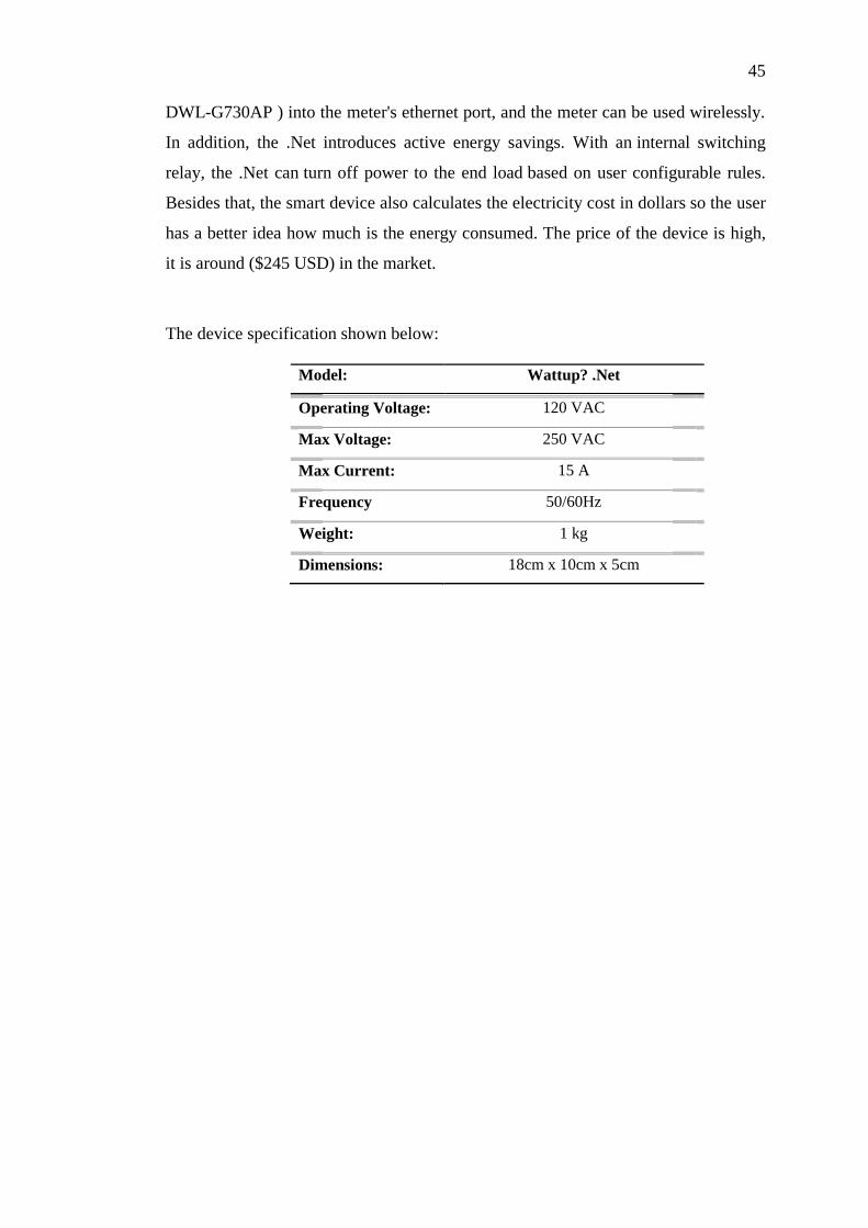
45
DWL-G730AP ) into the meter's ethernet port, and the meter can be used wirelessly.
In addition, the .Net introduces active energy savings. With an internal switching
relay, the .Net can turn off power to the end load based on user configurable rules.
Besides that, the smart device also calculates the electricity cost in dollars so the user
has a better idea how much is the energy consumed. The price of the device is high,
it is around ($245 USD) in the market.
The device specification shown below:
Model: Wattup? .Net
Operating Voltage: 120 VAC
Max Voltage: 250 VAC
Max Current: 15 A
Frequency 50/60Hz
Weight: 1 kg
Dimensions: 18cm x 10cm x 5cm
46
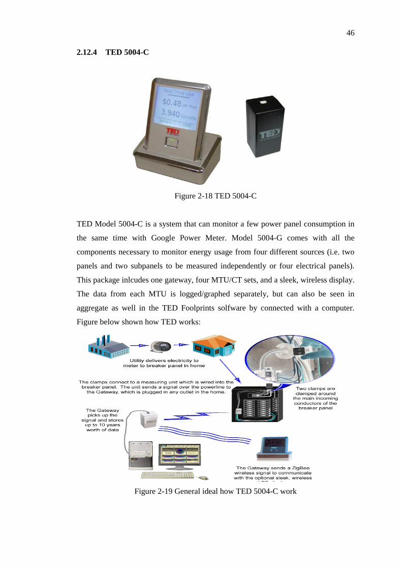
2.12.4 TED 5004-C
Figure 2-18 TED 5004-C
TED Model 5004-C is a system that can monitor a few power panel consumption in
the same time with Google Power Meter. Model 5004-G comes with all the
components necessary to monitor energy usage from four different sources (i.e. two
panels and two subpanels to be measured independently or four electrical panels).
This package inlcudes one gateway, four MTU/CT sets, and a sleek, wireless display.
The data from each MTU is logged/graphed separately, but can also be seen in
aggregate as well in the TED Foolprints solfware by connected with a computer.
Figure below shown how TED works:
Figure 2-19 General ideal how TED 5004-C work
47
2.13 Hardware and component
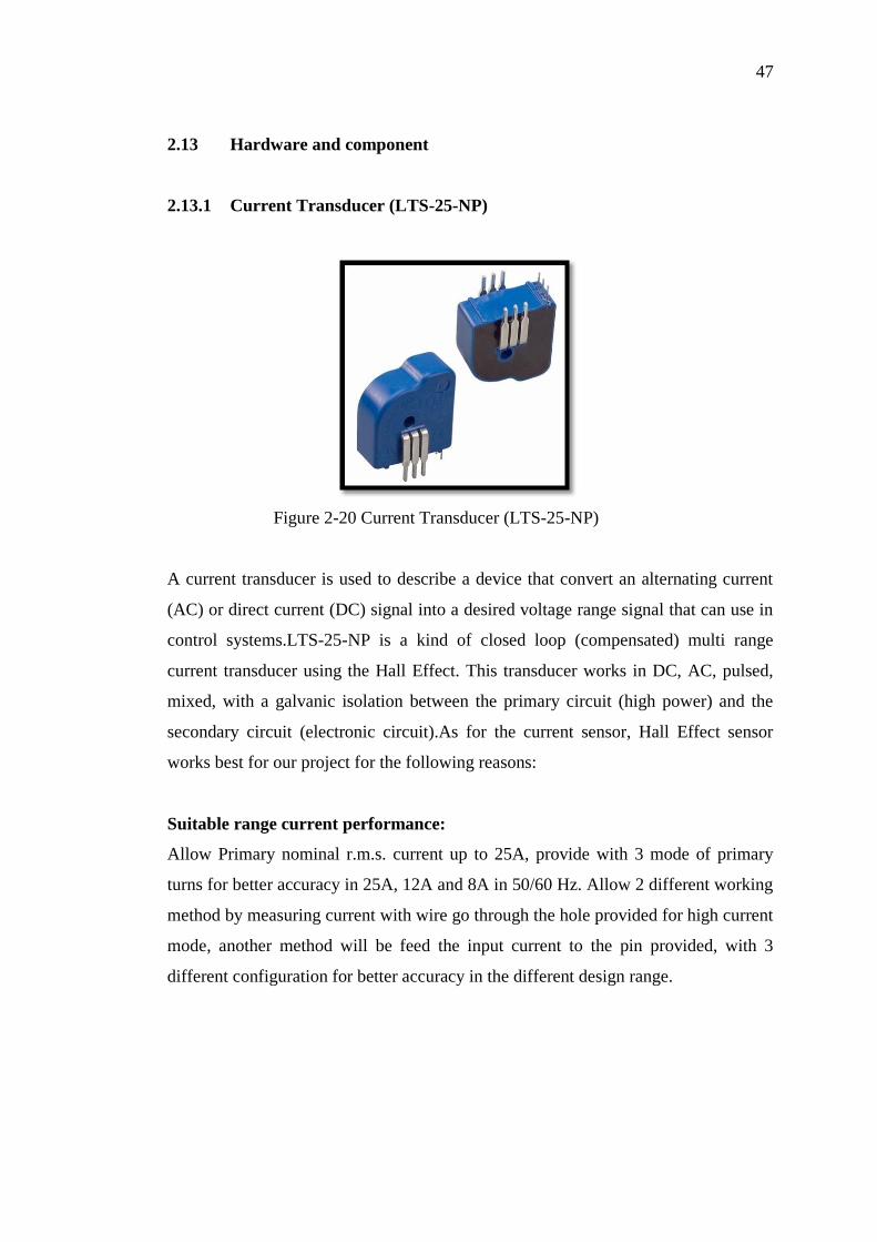
2.13.1 Current Transducer (LTS-25-NP)
Figure 2-20 Current Transducer (LTS-25-NP)
A current transducer is used to describe a device that convert an alternating current
(AC) or direct current (DC) signal into a desired voltage range signal that can use in
control systems.LTS-25-NP is a kind of closed loop (compensated) multi range
current transducer using the Hall Effect. This transducer works in DC, AC, pulsed,
mixed, with a galvanic isolation between the primary circuit (high power) and the
secondary circuit (electronic circuit).As for the current sensor, Hall Effect sensor
works best for our project for the following reasons:
Suitable range current performance:
Allow Primary nominal r.m.s. current up to 25A, provide with 3 mode of primary
turns for better accuracy in 25A, 12A and 8A in 50/60 Hz. Allow 2 different working
method by measuring current with wire go through the hole provided for high current
mode, another method will be feed the input current to the pin provided, with 3
different configuration for better accuracy in the different design range.
48
Figure 2-21 Mode of operating
Good linearity:
From the data sheet it shown that LTS-25-NP having a good linearity in detecting
current with suitable output shown below:
Figure 2-22 Vout vs Ip
High accuracy:
Accuracy @ Ipn , T = 25°C ± 0.2 %
Accuracy with RIM @ Ipn , T = 25°C ± 0.7 %
Easy to operate and optimized response time:
Compact design for PCB mounting,
Reaction time @ 10 % of Ipn < 100 ns
Response time @ 90 % of Ipn < 400 ns
The LTS-25NP current transducer is used in current measurement module for first
prototype model of this project to sense the input current and output with desired
49
voltage to communicate with PIC microchip to perform the ADC and further
computation. But the result is not as what we expected, therefore instead of using
current transducer, current transformer is used for the second prototype design.
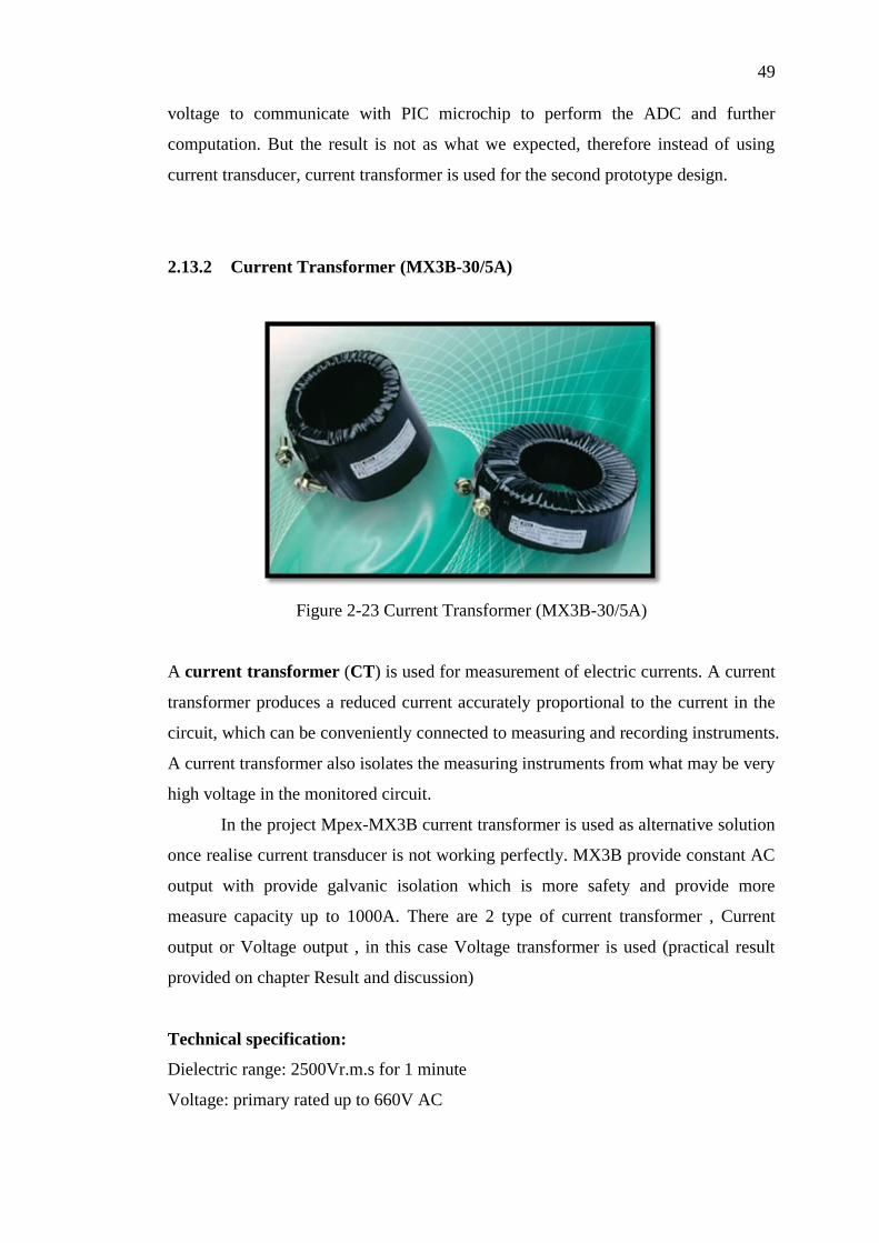
2.13.2 Current Transformer (MX3B-30/5A)
Figure 2-23 Current Transformer (MX3B-30/5A)
A current transformer (CT) is used for measurement of electric currents. A current
transformer produces a reduced current accurately proportional to the current in the
circuit, which can be conveniently connected to measuring and recording instruments.
A current transformer also isolates the measuring instruments from what may be very
high voltage in the monitored circuit.
In the project Mpex-MX3B current transformer is used as alternative solution
once realise current transducer is not working perfectly. MX3B provide constant AC
output with provide galvanic isolation which is more safety and provide more
measure capacity up to 1000A. There are 2 type of current transformer , Current
output or Voltage output , in this case Voltage transformer is used (practical result
provided on chapter Result and discussion)
Technical specification:
Dielectric range: 2500Vr.m.s for 1 minute
Voltage: primary rated up to 660V AC
50
Rated short time current: 2000 Amps for 1 second
Frequency: 50/60Hz
Temperature: -20 to 70 degree celcius
Insulation: class B
2.13.3 Microcontroller (PIC 16F877A)
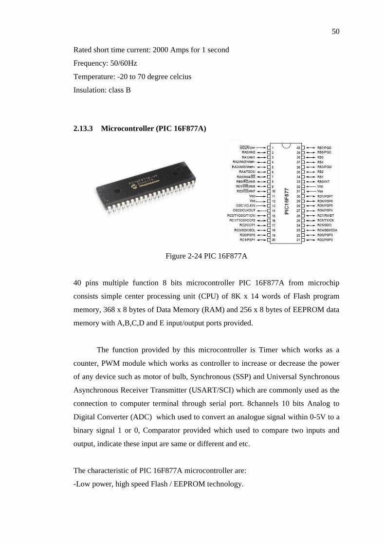
Figure 2-24 PIC 16F877A
40 pins multiple function 8 bits microcontroller PIC 16F877A from microchip
consists simple center processing unit (CPU) of 8K x 14 words of Flash program
memory, 368 x 8 bytes of Data Memory (RAM) and 256 x 8 bytes of EEPROM data
memory with A,B,C,D and E input/output ports provided.
The function provided by this microcontroller is Timer which works as a
counter, PWM module which works as controller to increase or decrease the power
of any device such as motor of bulb, Synchronous (SSP) and Universal Synchronous
Asynchronous Receiver Transmitter (USART/SCI) which are commonly used as the
connection to computer terminal through serial port. 8channels 10 bits Analog to
Digital Converter (ADC) which used to convert an analogue signal within 0-5V to a
binary signal 1 or 0, Comparator provided which used to compare two inputs and
output, indicate these input are same or different and etc.
The characteristic of PIC 16F877A microcontroller are:
-Low power, high speed Flash / EEPROM technology.
51
-Easy to design and reasonable price.
-Wide operating range (2.0V to 5.5V)
-Commercial and industrial operating temperature range
Personal review:
I have decided to use this microcontroller in the project as main control unit, perform
with inputs variables, logical processing, and output control. More detail will be
discussed in coming chapter.
2.14 Voltage regulator
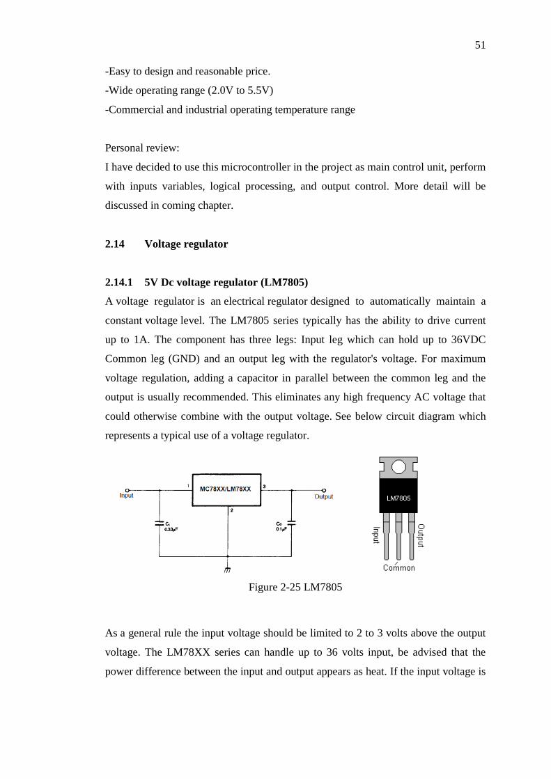
2.14.1 5V Dc voltage regulator (LM7805)
A voltage regulator is an electrical regulator designed to automatically maintain a
constant voltage level. The LM7805 series typically has the ability to drive current
up to 1A. The component has three legs: Input leg which can hold up to 36VDC
Common leg (GND) and an output leg with the regulator's voltage. For maximum
voltage regulation, adding a capacitor in parallel between the common leg and the
output is usually recommended. This eliminates any high frequency AC voltage that
could otherwise combine with the output voltage. See below circuit diagram which
represents a typical use of a voltage regulator.
Figure 2-25 LM7805
As a general rule the input voltage should be limited to 2 to 3 volts above the output
voltage. The LM78XX series can handle up to 36 volts input, be advised that the
power difference between the input and output appears as heat. If the input voltage is
52
unnecessarily high, the regulator will overheat. Unless sufficient heat dissipation is
provided through heat sinking, the regulator will shut down.
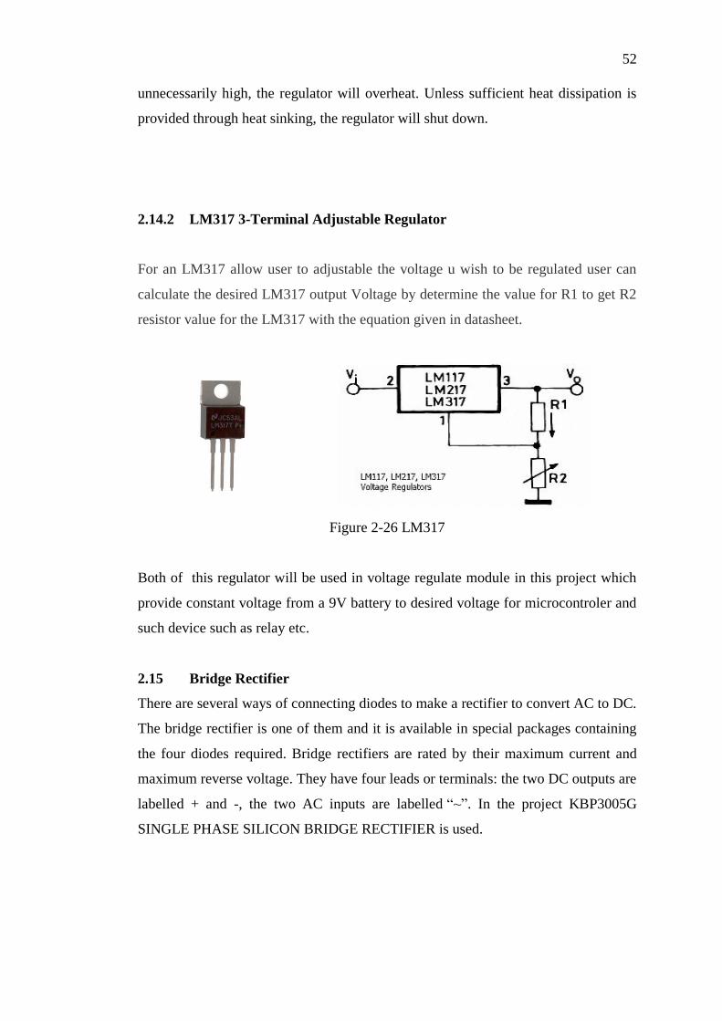
2.14.2 LM317 3-Terminal Adjustable Regulator
For an LM317 allow user to adjustable the voltage u wish to be regulated user can
calculate the desired LM317 output Voltage by determine the value for R1 to get R2
resistor value for the LM317 with the equation given in datasheet.
Figure 2-26 LM317
Both of this regulator will be used in voltage regulate module in this project which
provide constant voltage from a 9V battery to desired voltage for microcontroler and
such device such as relay etc.
2.15 Bridge Rectifier
There are several ways of connecting diodes to make a rectifier to convert AC to DC.
The bridge rectifier is one of them and it is available in special packages containing
the four diodes required. Bridge rectifiers are rated by their maximum current and
maximum reverse voltage. They have four leads or terminals: the two DC outputs are
labelled + and -, the two AC inputs are labelled “~”. In the project KBP3005G
SINGLE PHASE SILICON BRIDGE RECTIFIER is used.
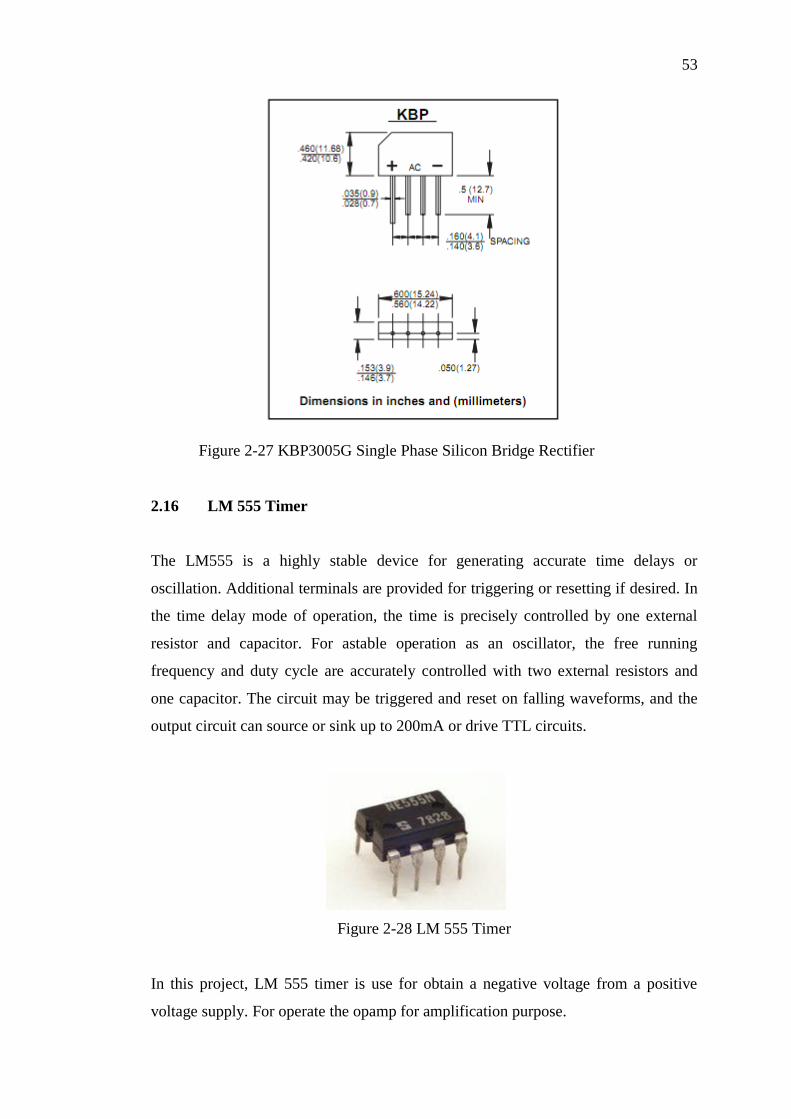
53
Figure 2-27 KBP3005G Single Phase Silicon Bridge Rectifier
2.16 LM 555 Timer
The LM555 is a highly stable device for generating accurate time delays or
oscillation. Additional terminals are provided for triggering or resetting if desired. In
the time delay mode of operation, the time is precisely controlled by one external
resistor and capacitor. For astable operation as an oscillator, the free running
frequency and duty cycle are accurately controlled with two external resistors and
one capacitor. The circuit may be triggered and reset on falling waveforms, and the
output circuit can source or sink up to 200mA or drive TTL circuits.
Figure 2-28 LM 555 Timer
In this project, LM 555 timer is use for obtain a negative voltage from a positive
voltage supply. For operate the opamp for amplification purpose.
54
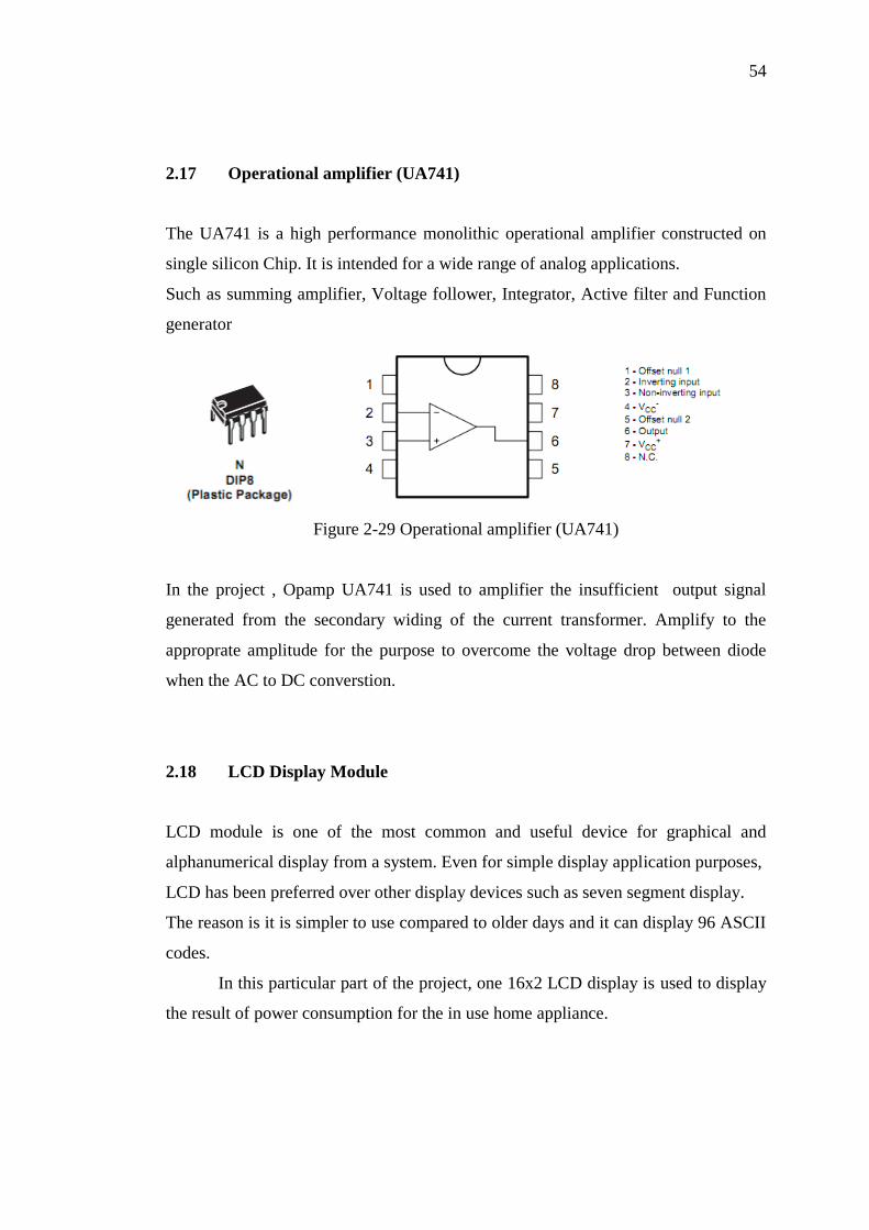
2.17 Operational amplifier (UA741)
The UA741 is a high performance monolithic operational amplifier constructed on
single silicon Chip. It is intended for a wide range of analog applications.
Such as summing amplifier, Voltage follower, Integrator, Active filter and Function
generator
Figure 2-29 Operational amplifier (UA741)
In the project , Opamp UA741 is used to amplifier the insufficient output signal
generated from the secondary widing of the current transformer. Amplify to the
approprate amplitude for the purpose to overcome the voltage drop between diode
when the AC to DC converstion.
2.18 LCD Display Module
LCD module is one of the most common and useful device for graphical and
alphanumerical display from a system. Even for simple display application purposes,
LCD has been preferred over other display devices such as seven segment display.
The reason is it is simpler to use compared to older days and it can display 96 ASCII
codes.
In this particular part of the project, one 16x2 LCD display is used to display
the result of power consumption for the in use home appliance.

55
Figure 2-30 16x2 LCD Display
2.19 Software
2.19.1 NI Ultiboard
Figure 2-31 NI Ultiboard 10
NI Ultiboard or formerly ULTIboard is an electronic Printed Circuit Board Layout
program which is part of a suite of circuit design programs, along with NI Multisim.
One of its major features is the Real Time Design Rule Check, a feature that was
only offered on expensive work stations in the days when it was introduced.
ULTIboard was originally created by a company named Ultimate Technology, which
is now a subsidiary of National Instruments. Ultiboard includes a 3D PCB viewing
mode, as well as integrated import and export features to the Schematic Capture and
Simulation software in the suite, Multisim (National Instruments, 2010). In the
project this software is used PCB design purpose.
56
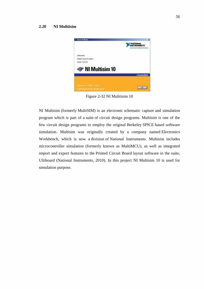
2.20 NI Mulitisim
Figure 2-32 NI Mulitisim 10
NI Multisim (formerly MultiSIM) is an electronic schematic capture and simulation
program which is part of a suite of circuit design programs. Multisim is one of the
few circuit design programs to employ the original Berkeley SPICE based software
simulation. Multisim was originally created by a company named Electronics
Workbench, which is now a division of National Instruments. Multisim includes
microcontroller simulation (formerly known as MultiMCU), as well as integrated
import and export features to the Printed Circuit Board layout software in the suite,
Ultiboard (National Instruments, 2010). In this project NI Multisim 10 is used for
simulation purpose.
57
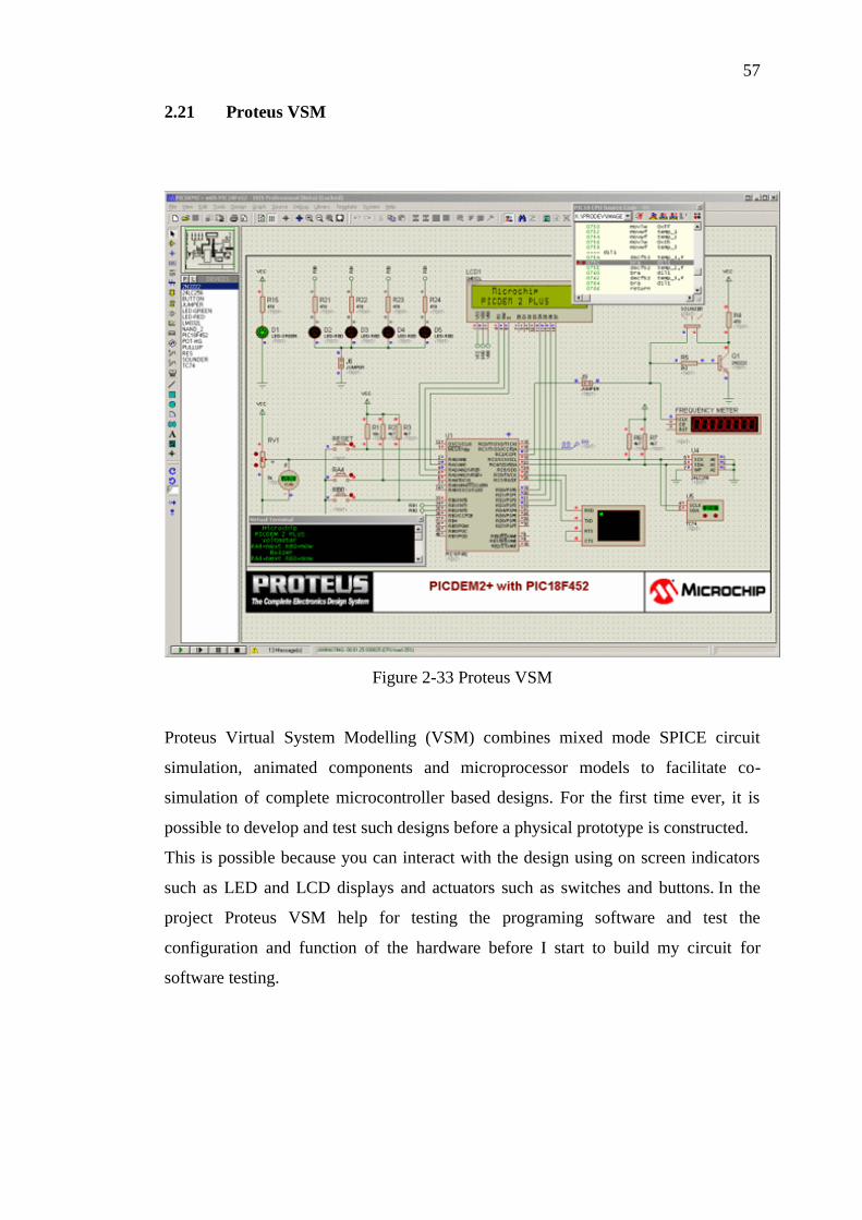
2.21 Proteus VSM
Figure 2-33 Proteus VSM
Proteus Virtual System Modelling (VSM) combines mixed mode SPICE circuit
simulation, animated components and microprocessor models to facilitate co-
simulation of complete microcontroller based designs. For the first time ever, it is
possible to develop and test such designs before a physical prototype is constructed.
This is possible because you can interact with the design using on screen indicators
such as LED and LCD displays and actuators such as switches and buttons. In the
project Proteus VSM help for testing the programing software and test the
configuration and function of the hardware before I start to build my circuit for
software testing.

58
2.22 MPLAB IDE
Figure 2-34 MPLAB IDE interface
MPLAB Integrated Development Environment (IDE) is a free, integrated toolset for
the development of embedded applications employing Microchip's PIC® and dsPIC®
microcontrollers. MPLAB IDE runs as a 32-bit application on MS Windows®, is
easy to use and includes a host of free software components for fast application
development and super-charged debugging. MPLAB IDE also serves as a single,
unified graphical user interface for additional Microchip and third party software and
hardware development tools. Moving between tools is a snap, and upgrading from
the free software simulator to hardware debug and programming tools is done in a
flash because MPLAB IDE has the same user interface for all tools (Microchip,
2010). MPLAB IDE software is the main development used in this project to develop
the system instruction.

59
2.23 CCS C Compiler
Figure 2-35 CSS compiler
Intelligent and highly optimized CCS C compilers contain Standard C operators and
Built-in Function libraries that are specific to PIC registers, providing developers
with a powerful tool for accessing device hardware features from the C language
level. Standard C pre-processors, operators and statements can be combined with
hardware specific directives and CCS provided built-in functions and example
libraries to quickly develop applications incorporating leading edge technologies
such as capacitive touch, wireless and wired communication, motion and motor
control and energy management.
In the project CCS built-in function such as ADC , LCD display modules are used to
make my programing more easy to be perform and save a lot steps of
troubleshooting
60
CHAPTER 3
3 METHODOLOGY
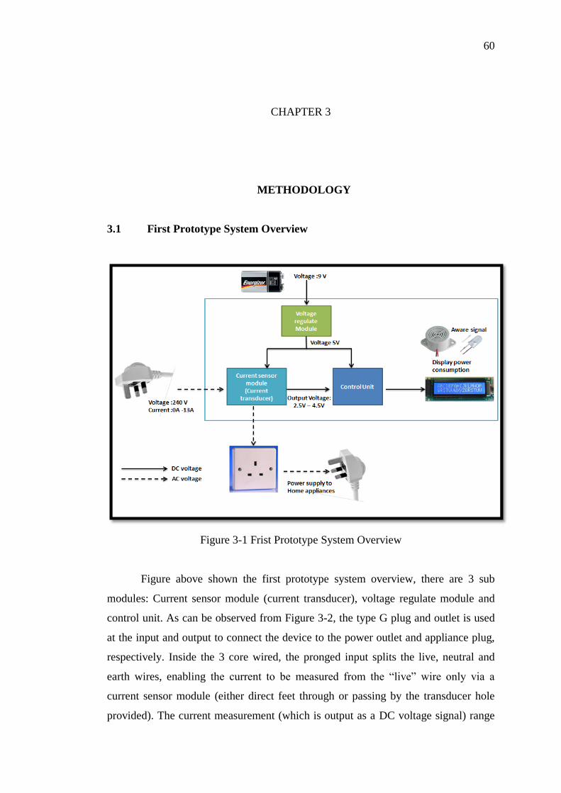
3.1 First Prototype System Overview
Figure 3-1 Frist Prototype System Overview
Figure above shown the first prototype system overview, there are 3 sub
modules: Current sensor module (current transducer), voltage regulate module and
control unit. As can be observed from Figure 3-2, the type G plug and outlet is used
at the input and output to connect the device to the power outlet and appliance plug,
respectively. Inside the 3 core wired, the pronged input splits the live, neutral and
earth wires, enabling the current to be measured from the “live” wire only via a
current sensor module (either direct feet through or passing by the transducer hole
provided). The current measurement (which is output as a DC voltage signal) range
61
2.5V to 4.5V will be converted to digital signal which perform by control unit (PIC)
for analog to digital conversion. Control unit will be performing various functions
such as process with power consumption calculation, timer, alert signal and display
total power consumption show from the LCD display and alert signal will be given
once the current or power exceed the desire pre-set limit. Voltage regulate module is
designed to provide a constant voltage level from 9V battery to 5V which is the
standard voltage for operating current sensor module and control unit which already
stated in datasheet provided.
3.2 First Prototype Hardware implementation
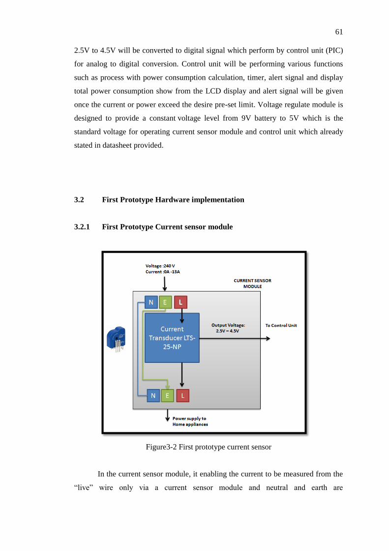
3.2.1 First Prototype Current sensor module
Figure3-2 First prototype current sensor
In the current sensor module, it enabling the current to be measured from the
“live” wire only via a current sensor module and neutral and earth are
62
interconnecting to the outlet to the home appliance plug. Current transducer LTS-25-
NP is used provided with 3 modes of primary turns for better accuracy. In this
project mode 2 is chosen in the range of 12A which is suitable supply for home
appliances. Output with linear voltage depends on detected current (0-12A) with a
range of 2.5V-4.5V.
The current sensor outputs a voltage proportional to the root-mean-square
(rms) current of the AC circuit. Using a constant voltage of 240 volts, power
consumption can be calculated using the rms current. Unfortunately, this value will
only be accurate for purely resistive loads. Reactive loads which contain capacitors
or inductors will induce a phase lag between the voltage and current waveforms. The
apparent power, which is what we are measuring with the current sensor, is actually
greater than the real power that is being used by the circuit.
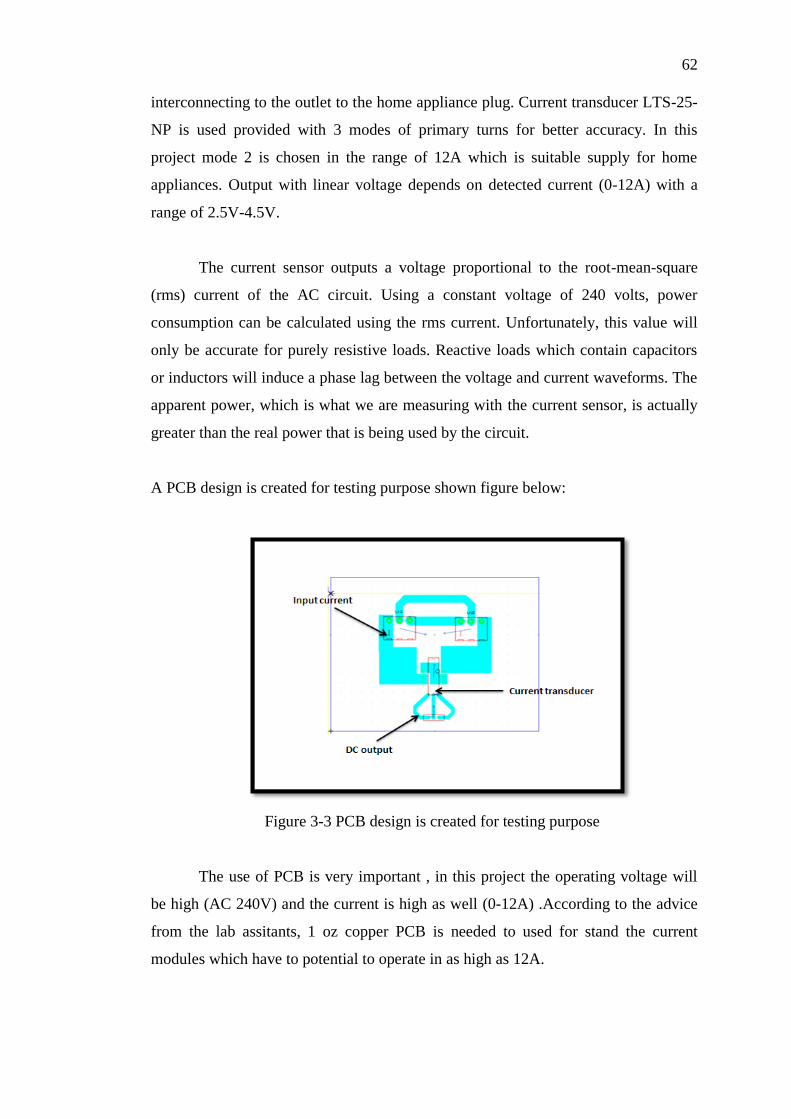
A PCB design is created for testing purpose shown figure below:
Figure 3-3 PCB design is created for testing purpose
The use of PCB is very important , in this project the operating voltage will
be high (AC 240V) and the current is high as well (0-12A) .According to the advice
from the lab assitants, 1 oz copper PCB is needed to used for stand the current
modules which have to potential to operate in as high as 12A.

63
Kinsten 1 Oz cooper PCB shown figure bellow is used for the high current
measurement design.
3.2.2 Voltage regulate module
Figure shows the circuit of the voltage regulator. In the circuit, LM7805 is used for
regulate the input voltage 9V from battery to 5V output voltage. This circuit is design
for regulate and stabilize the input voltage to the constant regulated output voltage as
the input supply to the PIC which is control unit module and the current sensor
module;. The constant input is very important to avoid the PIC microcontroller and
the sensor being over voltage and burned. The design of the circuit is able to give
about 150mA current, but it can be increased up to 1A when a good cooling is added
to the LM7805 regulator chip.
Figure 3-4 Schematic of Voltage regulator module
64
3.2.3 First prototype Control Unit overview
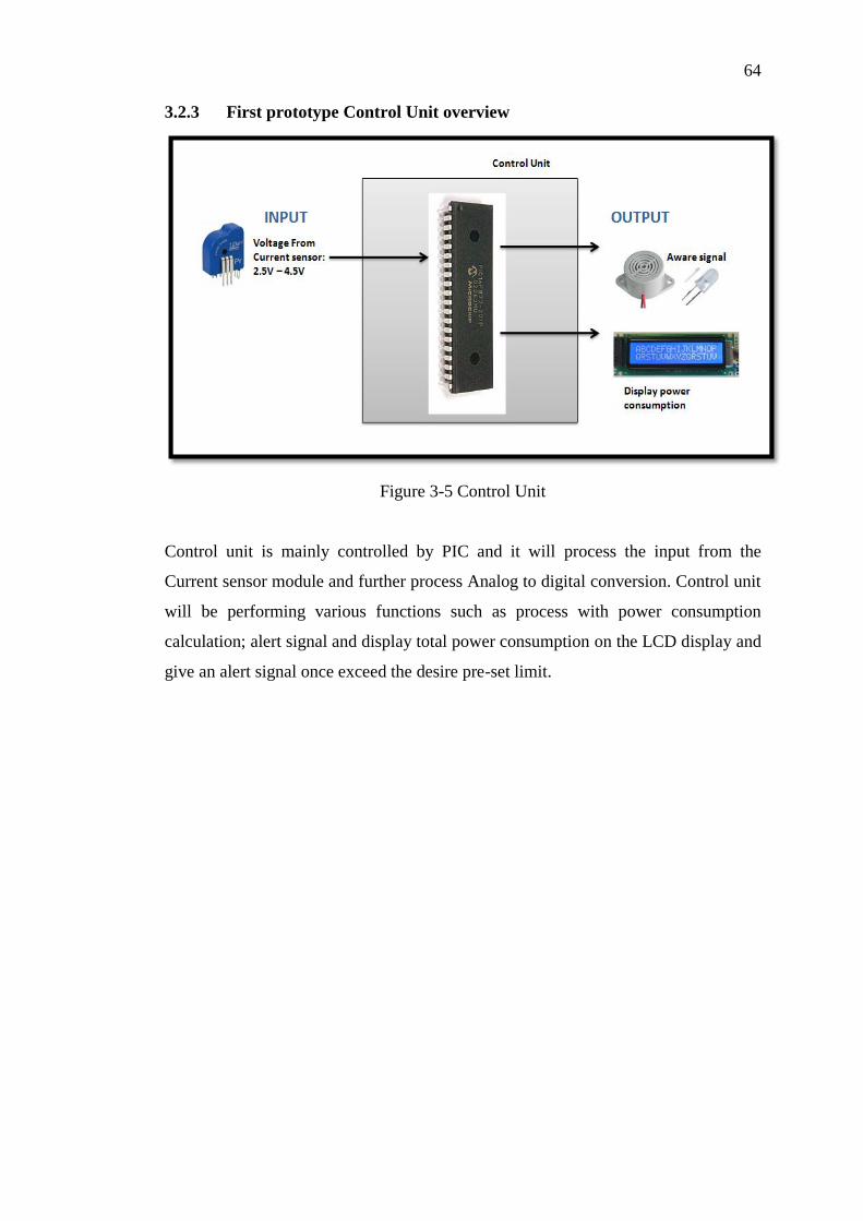
Figure 3-5 Control Unit
Control unit is mainly controlled by PIC and it will process the input from the
Current sensor module and further process Analog to digital conversion. Control unit
will be performing various functions such as process with power consumption
calculation; alert signal and display total power consumption on the LCD display and
give an alert signal once exceed the desire pre-set limit.
65
3.2.4 First prototype schematic
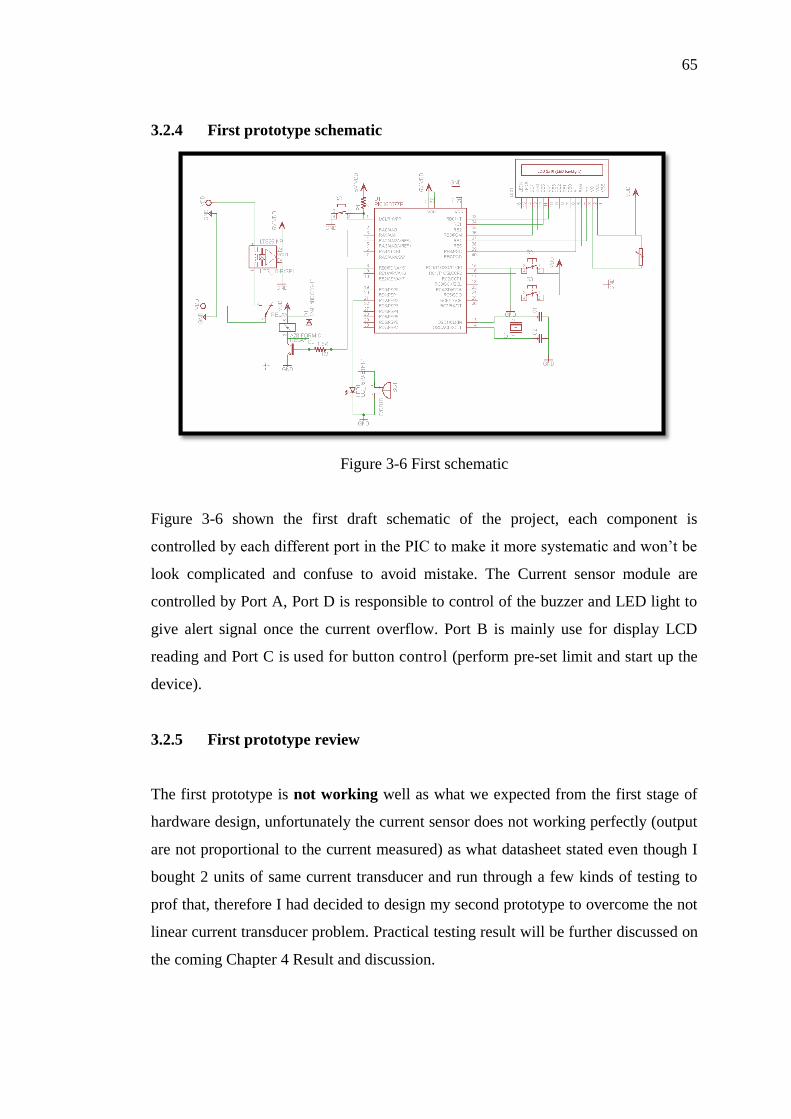
Figure 3-6 First schematic
Figure 3-6 shown the first draft schematic of the project, each component is
controlled by each different port in the PIC to make it more systematic and won’t be
look complicated and confuse to avoid mistake. The Current sensor module are
controlled by Port A, Port D is responsible to control of the buzzer and LED light to
give alert signal once the current overflow. Port B is mainly use for display LCD
reading and Port C is used for button control (perform pre-set limit and start up the
device).
3.2.5 First prototype review
The first prototype is not working well as what we expected from the first stage of
hardware design, unfortunately the current sensor does not working perfectly (output
are not proportional to the current measured) as what datasheet stated even though I
bought 2 units of same current transducer and run through a few kinds of testing to
prof that, therefore I had decided to design my second prototype to overcome the not
linear current transducer problem. Practical testing result will be further discussed on
the coming Chapter 4 Result and discussion.
66
3.3 Second prototype Hardware implementation
3.3.1 Second prototype system overview
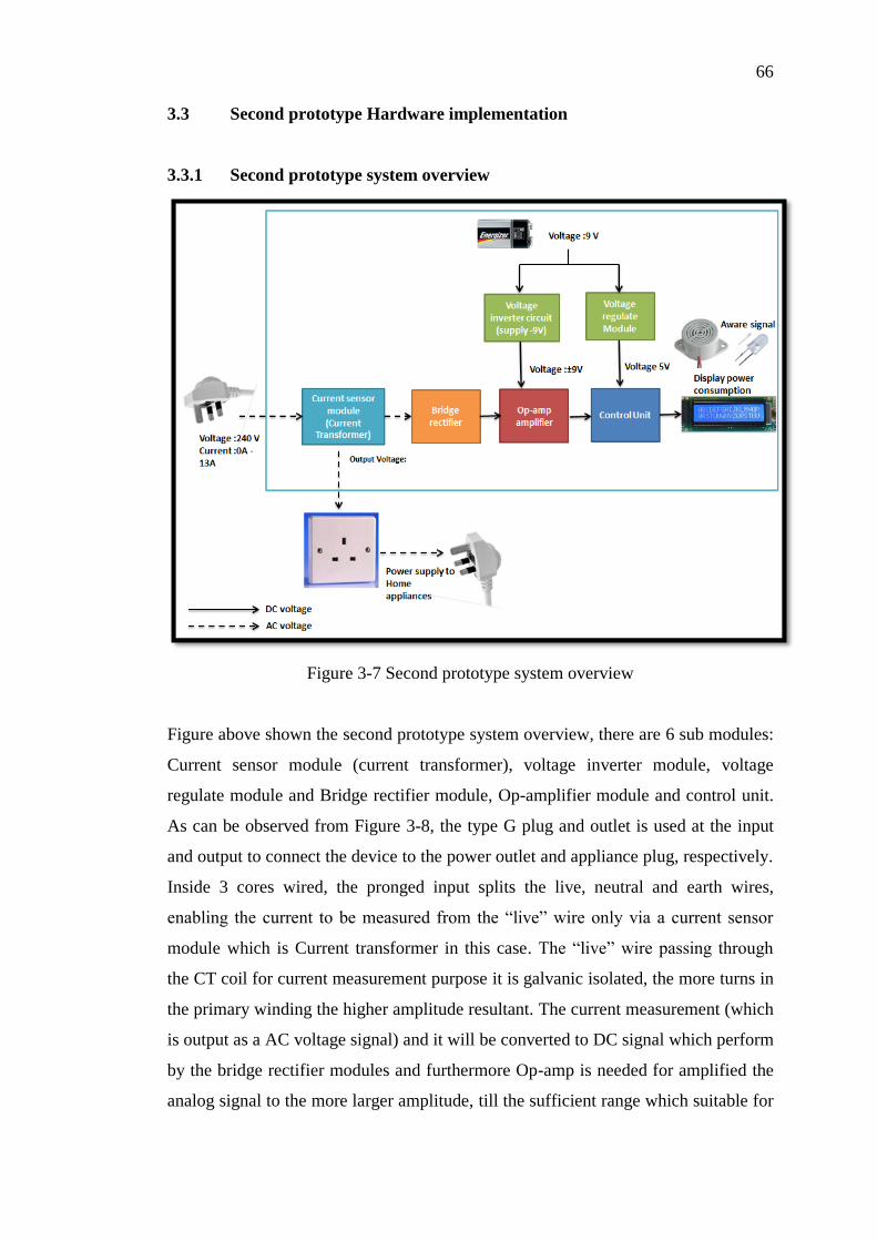
Figure 3-7 Second prototype system overview
Figure above shown the second prototype system overview, there are 6 sub modules:
Current sensor module (current transformer), voltage inverter module, voltage
regulate module and Bridge rectifier module, Op-amplifier module and control unit.
As can be observed from Figure 3-8, the type G plug and outlet is used at the input
and output to connect the device to the power outlet and appliance plug, respectively.
Inside 3 cores wired, the pronged input splits the live, neutral and earth wires,
enabling the current to be measured from the “live” wire only via a current sensor
module which is Current transformer in this case. The “live” wire passing through
the CT coil for current measurement purpose it is galvanic isolated, the more turns in
the primary winding the higher amplitude resultant. The current measurement (which
is output as a AC voltage signal) and it will be converted to DC signal which perform
by the bridge rectifier modules and furthermore Op-amp is needed for amplified the
analog signal to the more larger amplitude, till the sufficient range which suitable for

67
analog to digital conversion which done by control unit. Control unit will be
performing various functions same as the first prototype Voltage regulate module is
designed to provide a constant voltage level from 9V battery to 5V which is the
standard voltage for operating current sensor module and control unit which same as
what first prototype did.
3.3.2 Second prototype Current Sensor with Bridge Rectifier Module
Figure 3-8 Current sensor with bridge rectifier design
In the second prototype design, current sensor module is changed to current
transformer instead of using current transducer. By the way, Dc voltage is needed for
Control unit for further process because PIC is only accepted with DC voltage but
not AC. In order to generate a DC signal from an AC current transformer for input to
PIC. The following circuit provides an accurate method for creating this DC signal.
The gain of the first stage is always kept at 1 or unity (R2 = R3) to guarantee
symmetry of the as a buffer .rectified waveform. R2 should be chosen at least 10
times greater than R1 for proper accuracy.
The gain of the second stage is R5/R4 + 1. This gain is chosen to get the desired
output DC voltage for the designed input voltage.
DC can be generated directly from R1 by applying the AC voltage to a diode bridge.
However, the AC voltage required to do AC to DC conversion must be greater than 2
diode voltage drops, or over 2 VAC due to the characteristic of diode and this is what
the problem I faced in the second prototype.

68
3.3.3 Second prototype Voltage inverter
Figure 3-9 Voltage inverter
This circuit diagram shows how to obtain a negative voltage from a positive voltage
supply to provide ±9V for operating the op-amp in the voltage inverter module. The
advantage of this circuit is that, the negative voltage together with the original
positive supply can be used to simulate a dual supply. The circuit is based on timer
IC NE555. The NE555 is wired as an astable multivibrator operating at around 1
KHz. The square wave output if available at pin no 3 of the IC. During the positive
half of the square wave, capacitor C3 charges through diode D2.When the output of
IC is at zero the C3 discharges through diode D2 and the capacitor C4 gets charged.
As a result of this the voltage at the junction of the anode of D1 and cathode of C4
will be always negative with respect to the ground.
3.3.4 Second prototype review
In the second prototype design, although the current sensor gives a resultant output
as proportional to the current measured, But the problem still exist due to the output
voltage from CT coil is too low. The AC voltage required doing AC to DC
conversion this must be greater than 2 diode voltage drops, or over 2 VAC therefore
the design need more higher voltage before it going to the bridge rectifier module,

69
practical result worked on second prototype will be further more discuss on coming
Chapter Result and discussion .
Therefore a little less changes is done in the third prototype design which is
amplified the CT coil output before go for AC to DC conversation by bridge rectifier
module.
3.4 Third prototype hardware implementation
3.4.1 Third prototype System overview
Figure 3-10Third prototype system overview
In third prototype design, a slightly changes has been made. The op-amp perform as
amplifier to amplified the output of CT coil before proceed to Bridge Rectifier for
AC to DC conversion, this method works well because the amplified signal which
fulfil the characteristic of diode which required doing AC to DC conversion need a
amplitude that greater than 2 diode voltage drops. Other than that, all the modules are
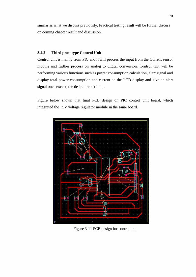
70
similar as what we discuss previously. Practical testing result will be further discuss
on coming chapter result and discussion.
3.4.2 Third prototype Control Unit
Control unit is mainly from PIC and it will process the input from the Current sensor
module and further process on analog to digital conversion. Control unit will be
performing various functions such as power consumption calculation, alert signal and
display total power consumption and current on the LCD display and give an alert
signal once exceed the desire pre-set limit.
Figure below shown that final PCB design on PIC control unit board, which
integrated the +5V voltage regulator module in the same board.
Figure 3-11 PCB design for control unit
71
3.5 Software implementation
Start
Key in desire
current or power
limit
Start up?
Exceed limit?
Display Current
and power wattage
Compute power
consumption
Reset?
Display Current
and power wattageAlert signal Exceed limit?
Y
N
Y
N
Y
N
Y
N
Figure 3-12 Flow chart of the software design
In the software design, C language was used with the CSS compiler which gives a lot
of convenient for me to configuring and implementing the software functions with
intergraded header libraries. The intergraded header library for PIC 16F877A is
provided with various function such as ADC, INTERUPTS, TIMER, LCD ext.
Therefore, ADC and LCD sub functions library was used in my programing coding.
72
Program source code:
73
74
First of all, the design started with the call function of 16F877A header which
provided a lot of useful sub function. In this case ADC and PIC initialisation sub
function is used. PIC oscillating speed is set as 20 MHz for high speed process
purpose.
LCDDRIVE.C is imported as a LCD driver for LCD display purpose. The main
program source start with initialisation of each parameter use either type of float or
int.
LCD and port initialisation is set as well as the input of the ADC and the sampling
rate. In this project, ADC input port is assigned to port A and analog input will be
detected by using the (Clock speed / 8) sampling time which mean process per
sampled by 0.4 µsec.
Initially, Welcome message displayed on LCD and ask for user to enter the
preference current limit.

75
A while loop is built to ensure the program is keep looping on it. Input is assigned
with desired pin for user to key in for the current limit and start the program.
“If” condition loop created, it function as increasing the current limit once the button
“increase” button is pressed, and continue with If statement of decreasing limit as
well.
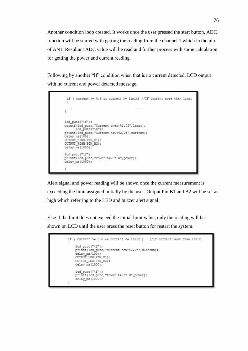
76
Another condition loop created. It works once the user pressed the start button, ADC
function will be started with getting the reading from the channel 1 which in the pin
of AN1. Resultant ADC value will be read and further process with some calculation
for getting the power and current reading.
Following by another “If” condition when that is no current detected, LCD output
with no current and power detected message.
Alert signal and power reading will be shown once the current measurement is
exceeding the limit assigned initially by the user. Output Pin B1 and B2 will be set as
high which referring to the LED and buzzer alert signal.
Else if the limit does not exceed the initial limit value, only the reading will be
shown on LCD until the user press the reset button for restart the system.
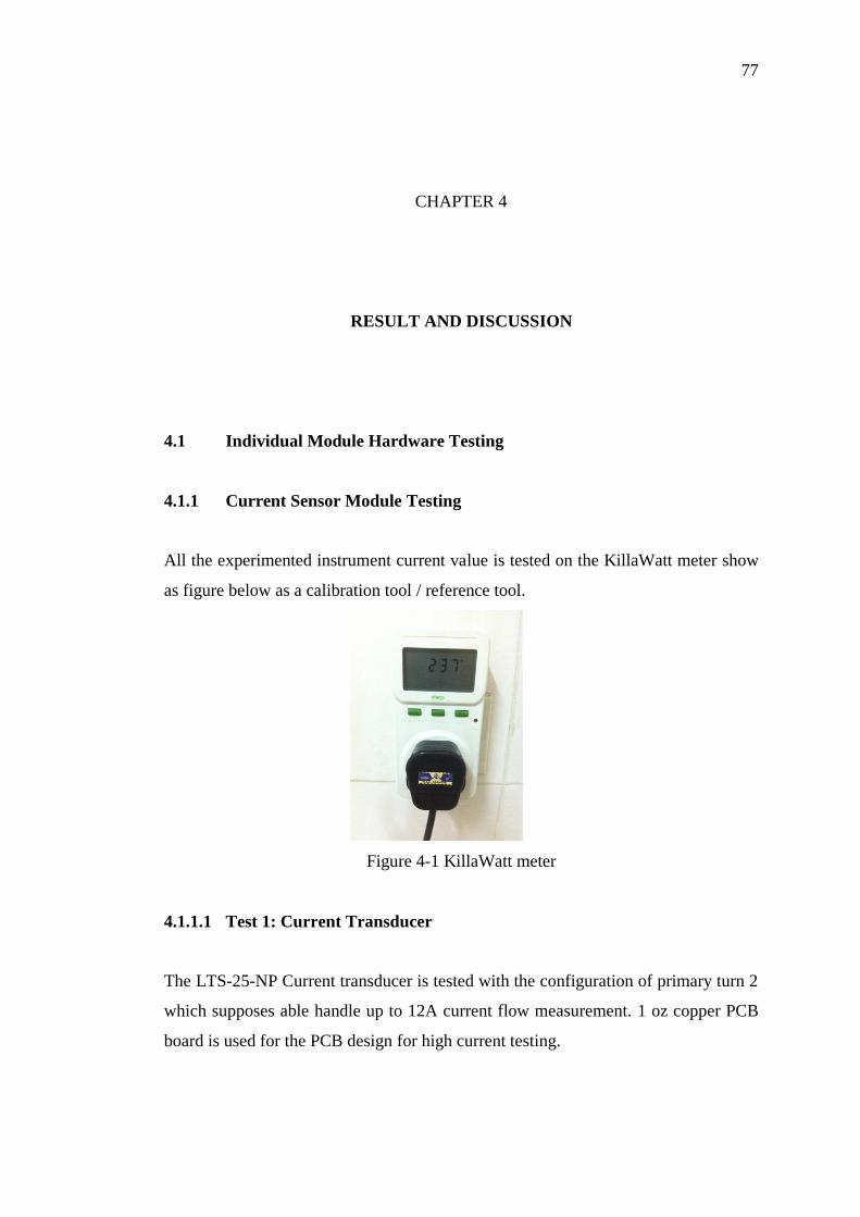
77
CHAPTER 4
RESULT AND DISCUSSION
4.1 Individual Module Hardware Testing
4.1.1 Current Sensor Module Testing
All the experimented instrument current value is tested on the KillaWatt meter show
as figure below as a calibration tool / reference tool.
Figure 4-1 KillaWatt meter
4.1.1.1 Test 1: Current Transducer
The LTS-25-NP Current transducer is tested with the configuration of primary turn 2
which supposes able handle up to 12A current flow measurement. 1 oz copper PCB
board is used for the PCB design for high current testing.
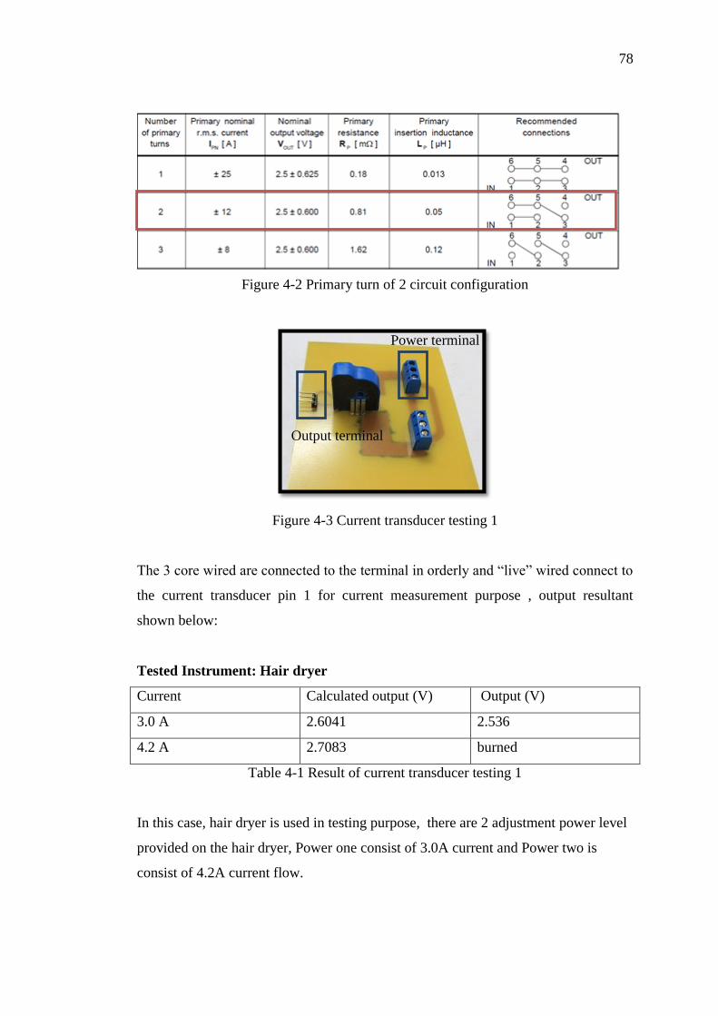
78
Figure 4-2 Primary turn of 2 circuit configuration
Figure 4-3 Current transducer testing 1
The 3 core wired are connected to the terminal in orderly and “live” wired connect to
the current transducer pin 1 for current measurement purpose , output resultant
shown below:
Tested Instrument: Hair dryer
Current Calculated output (V) Output (V)
3.0 A 2.6041 2.536
4.2 A 2.7083 burned
Table 4-1 Result of current transducer testing 1
In this case, hair dryer is used in testing purpose, there are 2 adjustment power level
provided on the hair dryer, Power one consist of 3.0A current and Power two is
consist of 4.2A current flow.
Power terminal
Output terminal

79
The current transducer provides an output of 2.536V for the measurement of 3.0A
which is not accurate as what we expected value of 2.604V provided from the
datasheet.
When we go for Power two which consist of 4.2A, the pin of component is burn with
spark, therefore no output is shown and I stop the experiment immediately for safety
purpose.
Figure: 4-4 PCB after sparking burn
The reason of spark occurs on board might because of the 6 pins is too near with
each other, with the measurement of high current, cause of the electromagnetic flux
is high therefore spark may occurred if the pins is not soldier well , it is dangerous
with testing on such high current in such a small board provided. Therefore, by
following the advice of my supervisor, instead of feeding the current through the
current transducer used alternative way for current measuring which is just passing
through the wire on the hole provided for safety purpose.
4.1.1.2 Test 2: Current Transducer
2nd method is experimented with passing through the “live” wire through the
measurement hole provided on LTS-25-NP shown as figure below:
Burn
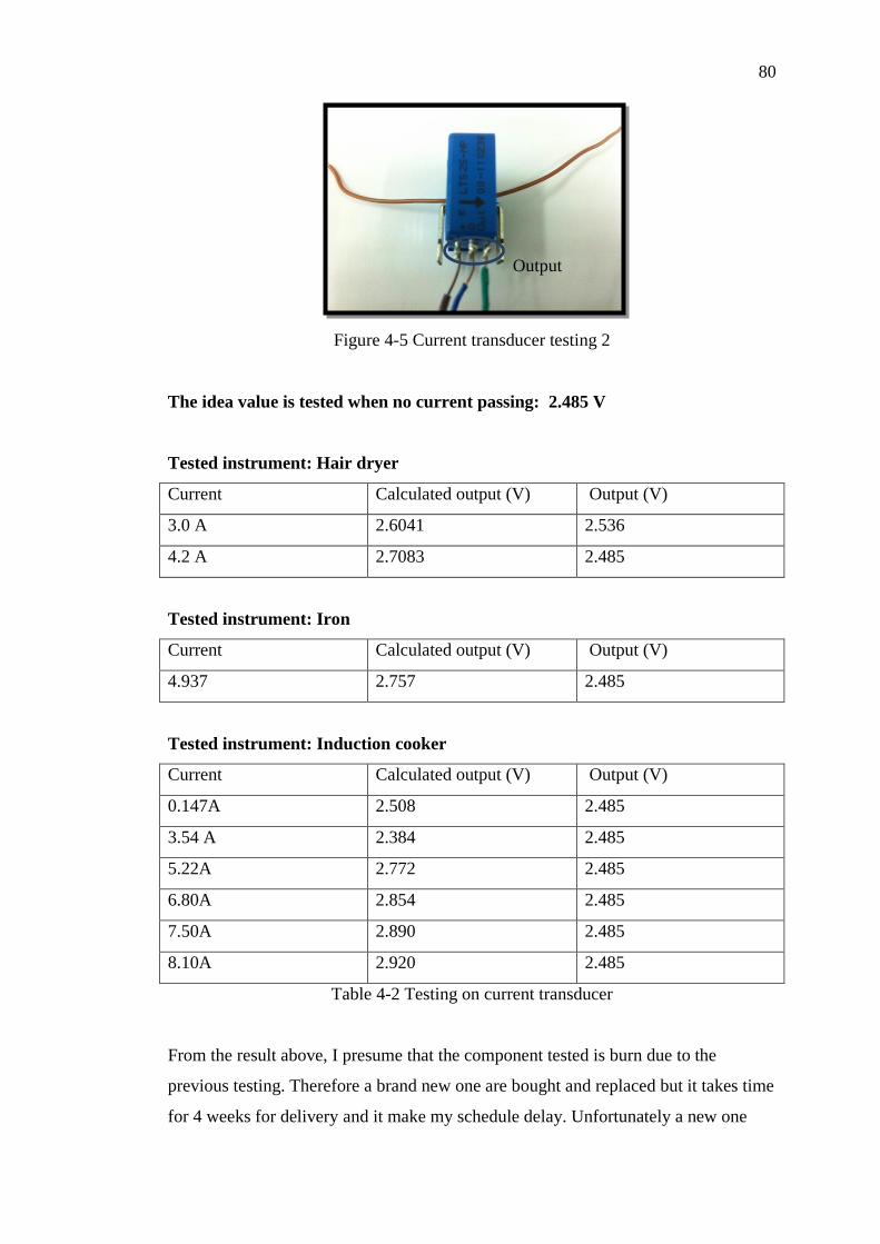
80
Figure 4-5 Current transducer testing 2
The idea value is tested when no current passing: 2.485 V
Tested instrument: Hair dryer
Current Calculated output (V) Output (V)
3.0 A 2.6041 2.536
4.2 A 2.7083 2.485
Tested instrument: Iron
Current Calculated output (V) Output (V)
4.937 2.757 2.485
Tested instrument: Induction cooker
Current Calculated output (V) Output (V)
0.147A 2.508 2.485
3.54 A 2.384 2.485
5.22A 2.772 2.485
6.80A 2.854 2.485
7.50A 2.890 2.485
8.10A 2.920 2.485
Table 4-2 Testing on current transducer
From the result above, I presume that the component tested is burn due to the
previous testing. Therefore a brand new one are bought and replaced but it takes time
for 4 weeks for delivery and it make my schedule delay. Unfortunately a new one
Output
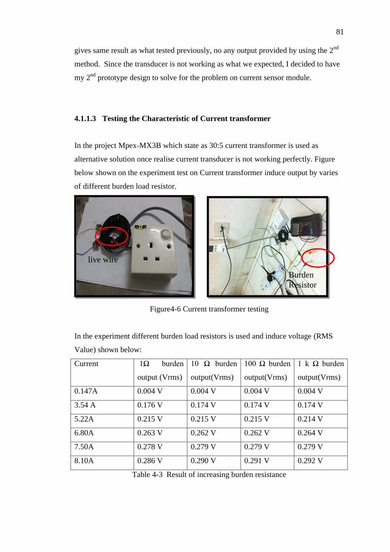
81
gives same result as what tested previously, no any output provided by using the 2nd
method. Since the transducer is not working as what we expected, I decided to have
my 2nd
prototype design to solve for the problem on current sensor module.
4.1.1.3 Testing the Characteristic of Current transformer
In the project Mpex-MX3B which state as 30:5 current transformer is used as
alternative solution once realise current transducer is not working perfectly. Figure
below shown on the experiment test on Current transformer induce output by varies
of different burden load resistor.
Figure4-6 Current transformer testing
In the experiment different burden load resistors is used and induce voltage (RMS
Value) shown below:
Current 1Ω burden
output (Vrms)
10 Ω burden
output(Vrms)
100 Ω burden
output(Vrms)
1 k Ω burden
output(Vrms)
0.147A 0.004 V 0.004 V 0.004 V 0.004 V
3.54 A 0.176 V 0.174 V 0.174 V 0.174 V
5.22A 0.215 V 0.215 V 0.215 V 0.214 V
6.80A 0.263 V 0.262 V 0.262 V 0.264 V
7.50A 0.278 V 0.279 V 0.279 V 0.279 V
8.10A 0.286 V 0.290 V 0.291 V 0.292 V
Table 4-3 Result of increasing burden resistance
Burden
Resistor
live wire

82
4-7 IV characteristic of Current transformer Mpex-MX3B
From the result, it can be conclude that that the current transformer is induce voltage
but not current. Although the output is not linear but at least it is proportional and
stable once the current increasing.
By increasing the primary turn of the current transformer, experimenting result
shown below:
Current 1Ω burden
output
(Vrms)
10 Ω burden
output(Vrms)
100 Ω burden
output(Vrms)
1 k Ω burden
output(Vrms)
0.147A 0.006 V 0.006 V 0.006 V 0.006 V
3.54 A 0.232 V 0.280 V 0.285 V 0.285 V
5.22A 0.292 V 0.330 V 0.334 V 0.333 V
6.80A 0.317 V 0.348 V 0.354 V 0.354 V
7.50A 0.325 V 0.356 V 0.361 V 0.360 V
8.10A 0.326 V 0.362 V 0.366 V 0.365 V
Table 4-4 Result of increase primary winding
From the result, the induce voltage is obviously increase after the primary turn is
increase to 2 instead of 1. We can conclude that the more the turn on primary side,
0
0.05
0.1
0.15
0.2
0.25
0.3
0.35
0.4
0 2 4 6 8 10
Vo
ltag
e
Current
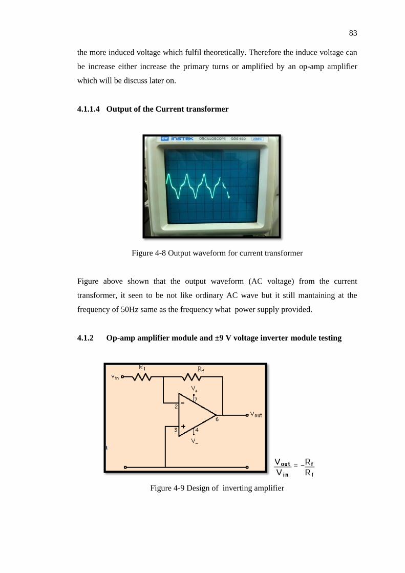
83
the more induced voltage which fulfil theoretically. Therefore the induce voltage can
be increase either increase the primary turns or amplified by an op-amp amplifier
which will be discuss later on.
4.1.1.4 Output of the Current transformer
Figure 4-8 Output waveform for current transformer
Figure above shown that the output waveform (AC voltage) from the current
transformer, it seen to be not like ordinary AC wave but it still mantaining at the
frequency of 50Hz same as the frequency what power supply provided.
4.1.2 Op-amp amplifier module and ±9 V voltage inverter module testing
Figure 4-9 Design of inverting amplifier

84
An inverting amplifier is designed , due to the low output of the current transformer
it need to be amplified to overcome the diode voltage drop problem in AC to DC
converstion. The ratio of mutiplier is depend on the design of R2 and R1 assigned,
result below shown the experimenting on resultant op-amp amplified output. The
input is simulated from function generator which provide 50Hz of AC voltage signal
and operating voltage ±9V from Dc power supply shown as figure shown below.
Figure 4-10 Instrument used in testing op-amp amplifier
4.1.2.1 Testing on Stability Op-amp amplifier module
Test 1
R1= 50Ω , R2= 1 kΩ , Amplified ratio= 20 times.
Input voltage ( AC peak to peak) Amplified voltage ( AC peak to peak)
0.1 Vpp 1.0 Vpp
0.2 Vpp 2.2 Vpp
0.3 Vpp 3.0 Vpp
0.4 Vpp 4.1 Vpp
Table 4-5 Amplifier testing 1
The experimented result is not same as what we expected which surpose 20 times
amplified theoritically,but resultant with only 10 times, the input is clipping half
wave once the op-amp power on, therefore I do recheck back with the op-amp and
realize that it is actually a standard requiment input resistance for the min of 100k
ohm and maximum 2Mohm. Thus resistance is replaced to fufill the requirement
standard.
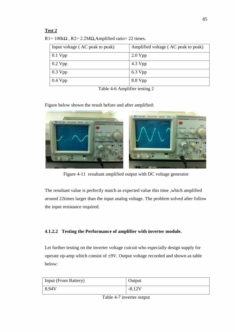
85
Test 2
R1= 100kΩ , R2= 2.2MΩ,Amplified ratio= 22 times.
Input voltage ( AC peak to peak) Amplified voltage ( AC peak to peak)
0.1 Vpp 2.0 Vpp
0.2 Vpp 4.3 Vpp
0.3 Vpp 6.3 Vpp
0.4 Vpp 8.8 Vpp
Table 4-6 Amplifier testing 2
Figure below shown the result before and after amplified:
Figure 4-11 resultant amplified output with DC voltage generator
The resultant value is perfectly match as expected value this time ,which amplified
around 22times larger than the input analog voltage. The problem solved after follow
the input resistance required.
4.1.2.2 Testing the Performance of amplifier with inverter module.
Let further testing on the inverter voltage cuicuit who especially design supply for
operate op-amp which consist of ±9V. Output voltage recorded and shown as table
below:
Input (From Battery) Output
8.94V -8.12V
Table 4-7 inverter output

86
The output voltage (inverted voltage) is not exactly same as the input voltage due to
the voltage drop between the components in the circuit design (loading effect). But it
is still acceptable and able to operate the op-amp perfectly , but the clipping issue is
concern. Therefore output of the inverting amplifier is tested by using the battery and
inverter circuit to operate the op-amp, and result shown in table below .
Figure 4-12 op-amp amplifier with ±9V voltage supply
Input voltage (AC) Amplified voltage(AC)
0.1 Vpp 2.0 Vpp
0.2 Vpp 4.4 Vpp
0.3 Vpp 6.4 Vpp
0.4 Vpp 8.0 Vpp (clipping)
Table 4-8 Amplified output with voltage inverter module
The clipping problem occurs once the amplified voltage more than the operating
voltage supply (8.12V), this is expected and this is the caution point for my system
design. Therefore the amplified circuit should be designed not as larger as this level.
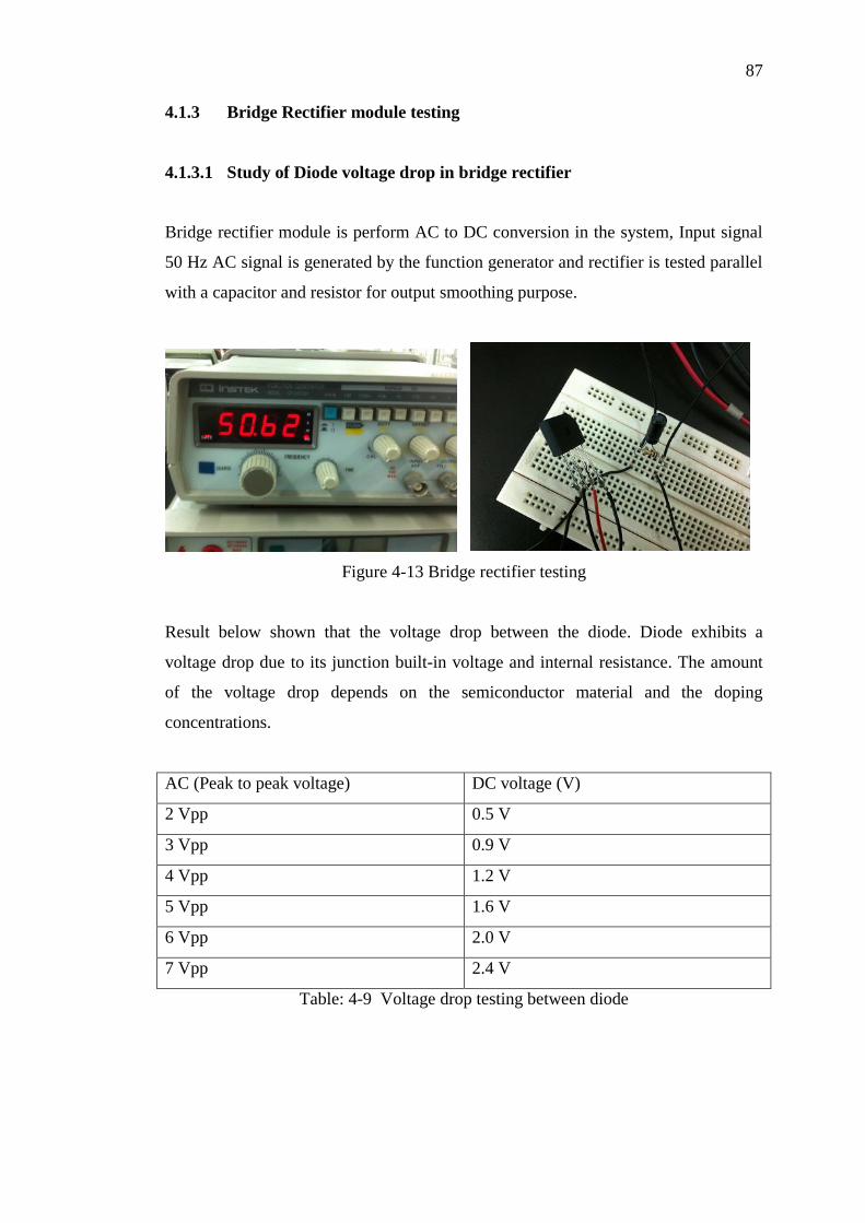
87
4.1.3 Bridge Rectifier module testing
4.1.3.1 Study of Diode voltage drop in bridge rectifier
Bridge rectifier module is perform AC to DC conversion in the system, Input signal
50 Hz AC signal is generated by the function generator and rectifier is tested parallel
with a capacitor and resistor for output smoothing purpose.
Figure 4-13 Bridge rectifier testing
Result below shown that the voltage drop between the diode. Diode exhibits a
voltage drop due to its junction built-in voltage and internal resistance. The amount
of the voltage drop depends on the semiconductor material and the doping
concentrations.
AC (Peak to peak voltage) DC voltage (V)
2 Vpp 0.5 V
3 Vpp 0.9 V
4 Vpp 1.2 V
5 Vpp 1.6 V
6 Vpp 2.0 V
7 Vpp 2.4 V
Table: 4-9 Voltage drop testing between diode
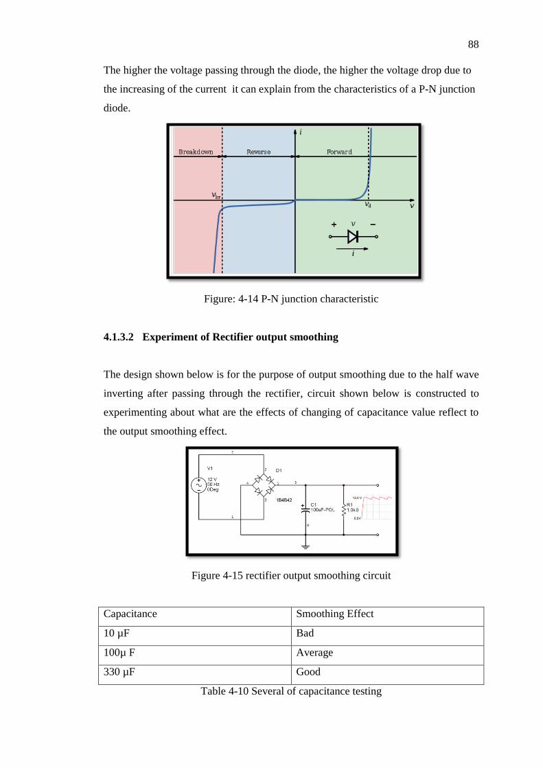
88
The higher the voltage passing through the diode, the higher the voltage drop due to
the increasing of the current it can explain from the characteristics of a P-N junction
diode.
Figure: 4-14 P-N junction characteristic
4.1.3.2 Experiment of Rectifier output smoothing
The design shown below is for the purpose of output smoothing due to the half wave
inverting after passing through the rectifier, circuit shown below is constructed to
experimenting about what are the effects of changing of capacitance value reflect to
the output smoothing effect.
Figure 4-15 rectifier output smoothing circuit
Capacitance Smoothing Effect
10 µF Bad
100µ F Average
330 µF Good
Table 4-10 Several of capacitance testing

89
Figure: 4-16 Resultant DC voltage by using 10 µF capacitance
Figure: 4-17 Resultant DC voltage by using 330 µF capacitance
From result above we can conclude that the larger capacitance in the design, the
smoothing the rectifier output DC voltage. A larger capacitor will reduce ripple but
will cost more and will create higher peak currents in the transformer secondary and
in the supply feeding it.
4.2 Combination modules testing
Experimenting of the combination modules which include current sensor, op-amp
amplifier, voltage inverter, bridge rectifier and control unit to test the link function of
each modules in the system. Figure below shown the configuration and connection
for the system
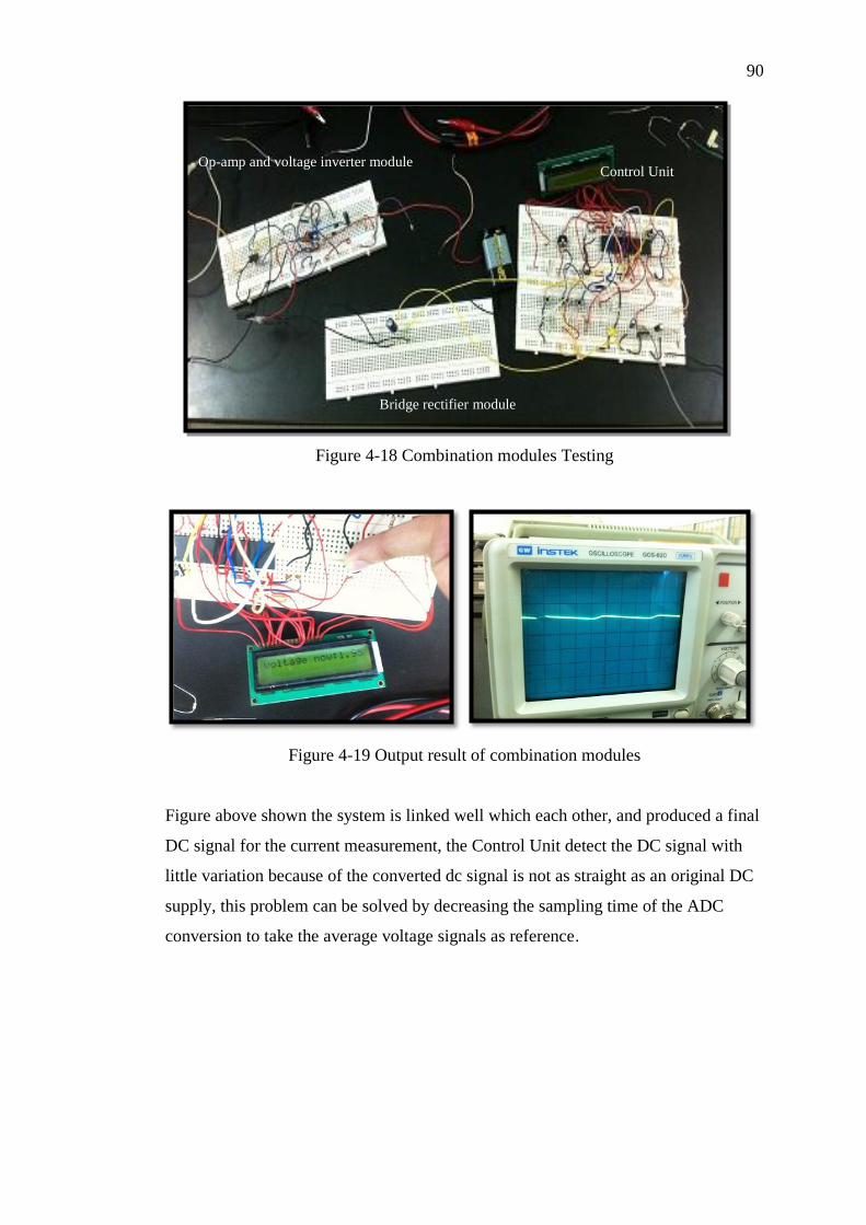
90
Figure 4-18 Combination modules Testing
Figure 4-19 Output result of combination modules
Figure above shown the system is linked well which each other, and produced a final
DC signal for the current measurement, the Control Unit detect the DC signal with
little variation because of the converted dc signal is not as straight as an original DC
supply, this problem can be solved by decreasing the sampling time of the ADC
conversion to take the average voltage signals as reference.
Op-amp and voltage inverter module
Bridge rectifier module
Control Unit
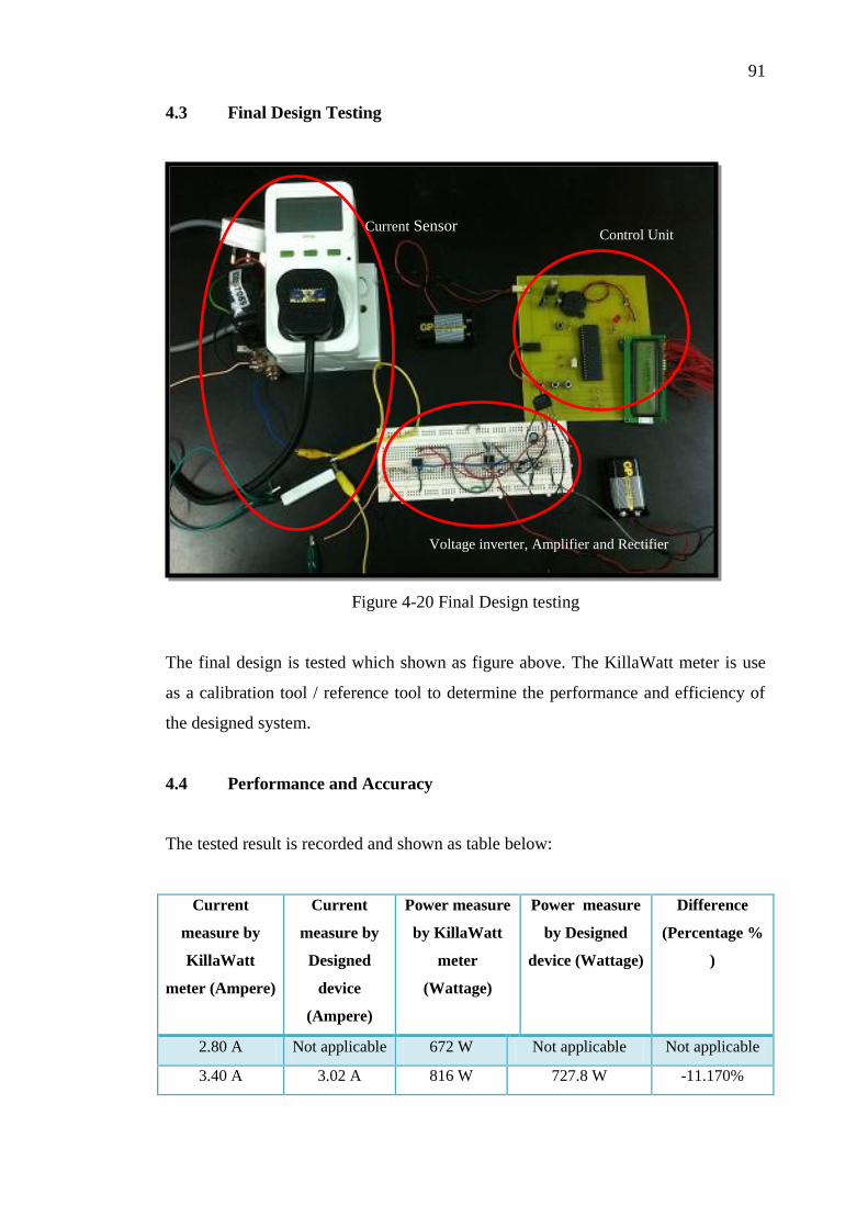
91
4.3 Final Design Testing
Figure 4-20 Final Design testing
The final design is tested which shown as figure above. The KillaWatt meter is use
as a calibration tool / reference tool to determine the performance and efficiency of
the designed system.
4.4 Performance and Accuracy
The tested result is recorded and shown as table below:
Current
measure by
KillaWatt
meter (Ampere)
Current
measure by
Designed
device
(Ampere)
Power measure
by KillaWatt
meter
(Wattage)
Power measure
by Designed
device (Wattage)
Difference
(Percentage %
)
2.80 A Not applicable 672 W Not applicable Not applicable
3.40 A 3.02 A 816 W 727.8 W -11.170%
Current Sensor Control Unit
Voltage inverter, Amplifier and Rectifier

92
4.20 A 4.10 A 1008 W 984 W +2.380%
5.00 A 5.50 A 1200 W 1320 W -10.000%
6.60 A 7.14 A 1584 W 1713.6 W +8.100%
7.32 A 7.60 A 1756.8 W 1824 W +3.825%
7.90 A 8.20 A 1896 W 1968 W +12.000%
Table 4-11 Performance and accuracy
From the result, we can conclude that the accuracy of the designed product is good
which only has the differences of ±10% by comparing with the commercial product.
The cons of the product is it only applicable for the measurement of current in the
range of 3A~10A.If the current below than 3A, the device will not be applicable to
detect.
The limitation and accuracy issues will be further discuss on the coming Chapter 5
Conclusion

93
CHAPTER 5
5 CONCLUSION
5.1 Limitation of the product
The limitation of the product is that is only applicable for the measurement of current
in the range of 3A~10A. Unfortunately it is not really a perfect design for the home
instrument power monitoring purpose which commonly in the range of 0-10A.
In the designed system, if the current below than 3A, the device are not able to detect.
It is due to the limitation of the current transformer (low sensitivity) and the design
which is more suitable performs for high current measurement (large capacity).
Another reason is that the output voltage from current sensor required doing AC to
DC conversion must be greater than 2 diode voltage drops in the rectifier module,
Once the current which pass through the CT coil is low (< 3A), the CT output with
induce low voltage (mile volt). Even though the output is amplified but it is still not
exceed of the voltage drop required of the diode.
The low current sensing can improve by adjusting the ratio of amplifying from the
output of the CT coiled to get the low current reading (<3A) but the high current
measuring problem occurs (>6A) once the amplified ratio is too high. It is because
the Op-amp Clipping problem that we have discussed, the amplified voltage will be
clipping at ±8V which is the maximum supply for the battery.
Thus I have decided to design for high current measuring instead of low current, it is
because of the higher power consumed device is more necessary for consumer to
monitoring and avoid energy wastage problem which obtained our main objective in
the project.

94
Secondly, the product efficiency which has a differences of ±10% by comparing with
the commercial product. The inaccuracy problem can be explained due to a few
factors.
1) The Transformer IV Characteristic which is not linear discussed previously, it
cause the difficulty to obtain a formula for power and current calculation in
the PIC calculation process.
2) The not ordinary AC output of the Current transformer.
3) The unstable Voltage DC output by the bridge rectifier.
Thirdly, the outlook and presentation of the product can be doing better. The final
product look complicated and not so compact Due to the sudden changing of my
hardware design the limitation of time, parts of my module are built on donut board
but not PCB.

95
5.2 Improvement
In the hardware implementation improvement, the limitation of the product is it only
applicable for the measurement of current in the range of 3A~10A due to the current
sensor module. To make a wider the range of current measurement, a better current
sensor needed. Instead of using such big size industrial used current transformer, it
can be improved by using current transducer or PCB type current transformer which
I am not able to get from the supplier. A better sensitivity and linear output current
sensor needed to have low current measuring (< 3A) to achieve higher accuracy.
In the software implementation improvement , it can be done my adding on some
extra feature such as timer and cost calculator , to getting know what is the time and
cost spend by the individual device.
For system further improvement, I suggest it can be further design with each power
monitoring system communicating with a main computer by wireless transmission
such as Xbee technology. Thus, the user can be fully monitoring the whole house
power expend and furthermore can be used for controlling (switch on and off) the
individually home appliance with the wireless technology.

96
5.3 Conclusion
The construction of real-time power monitoring system with user feedback is one
step in the larger process of reducing household energy consumption. All of the
elements of the feedback system must work together towards one common goal:
informing users of their energy consumption patterns such that they are continuously
motivated to adjust their behavior in sustainable ways. This knowledge will allow
users to identify trouble areas in their personal consumption, which in turn may lead
to them removing inefficient device and becoming more aware of conservation
techniques.
A real time power monitoring is developed with a measurement of current range of
3A to 10A, which capable measure up to 720W to 2400W power consumption which
is in a suitable range to detect home electrical appliances. The performance and
accuracy of the system is good which only has the differences of ±10% by comparing
with the commercial tested product.

97
REFERENCES
1. Morton, J. (1998). The PIC microcontroller: your personal introductory
course. Burlinton: Newnes.
2. Pugh, R. (2009, March 1st). Current and Power Waveform Measurement
Technique. pp. 1-2.
3. Robert Warren Erickson, D. M. (2004). Fundamentals of power electronics.
Norway: Kluwer acedemic publisher.
4. Arora, M. (2010, july 7). Retrieved from eetimes:
http://www.eetimes.com/design/industrial-control/4204841/Why-a-power-
factor-correction-device-is-better-suited-to-industrial-applications
5. Faisal, M. F. Voltage Sag Solution.
6. Korada, P. (n.d.). Hall Effect Current Sensors. Retrieved from magnelab:
http://www.magnelab.com/hall.pdf
7. M. Tavakoli Bina, A. K. (2011). International Journal of Electrical Power &
Energy Systems ,
http://www.energymanagertraining.com/announcements/EE08_result/C.Jayar
aman(1).pdf.
8. Microchip. (2010). Retrieved from http://www.microchip.com/
9. Mitzner, K. (2007). Complete PCB design using OrCad capture and layout.
Burlington: Newnes.
10. Morton, J. (1998). The PIC microcontroller: your personal introductory
course. Burlinton: Newnes.
11. Morton, J. (2005). The PIC microcontroller: your personal introductory
course. Newnes.
12. Nagrath. (2007). Electronic Devices and Circuits. PHI Learning Pvt. Ltd.
13. National Instruments. (2010). Retrieved from http://www.ni.com/multisim/
14. Nave, R. (n.d.). hyperphysics. Retrieved from http://hyperphysics.phy-
astr.gsu.edu/hbase/electronic/rectbr.html
15. Pugh, R. (2009, March 1st). Current and Power Waveform Measurement
Technique. pp. 1-2.

98
16. Robert Warren Erickson, D. M. (2004). Fundamentals of power electronics.
Norway: Kluwer acedemic publisher.
17. Systems, E. P. (2009). Electrical Power Systems. New Age International.
18. Vincent, J. (2009). flashscience. Retrieved from
http://www.flashscience.com/electricity/smoothing.htm
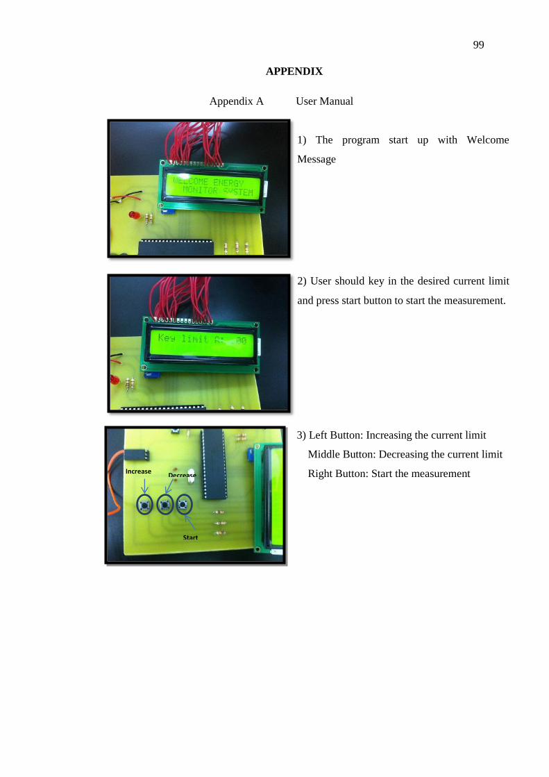
99
APPENDIX
Appendix A User Manual
Increase Decrease
Start
1) The program start up with Welcome
Message
2) User should key in the desired current limit
and press start button to start the measurement.
3) Left Button: Increasing the current limit
Middle Button: Decreasing the current limit
Right Button: Start the measurement
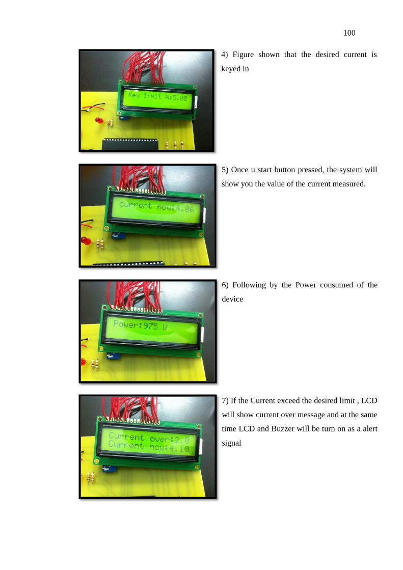
100
4) Figure shown that the desired current is
keyed in
5) Once u start button pressed, the system will
show you the value of the current measured.
6) Following by the Power consumed of the
device
7) If the Current exceed the desired limit , LCD
will show current over message and at the same
time LCD and Buzzer will be turn on as a alert
signal

101
Appendix B Time Scheduling
During the development process of the project, the uses of timeline planning are
important to make sure the flows of the process are smooth and completed in time.
Gantt chart is used for time scheduling management shown as figure below:
Figure 0-1 Project Gantt Chart
Task 1:
Literature
review
Task 2:
Analysis
process
Task 3:
Design
Task 4:Develop
and
implementation
Task 5:
Testing and
Debug
Task 6:Final
production and
Further
Enhancement
Start
Date
6/1/2010 7/6/2010 9/7/2010 11/26/2010 1/25/2011 3/16/2011
End Date 7/6/2010 9/7/2010 11/26/2010 1/25/2011 3/16/2011 5/15/2011
Duration
(days)
35
(5 Weeks)
63
(9 Weeks)
80
(11 Weeks)
70
(10 Weeks)
50
(7 Weeks)
50
(7 Weeks)
Table 0-1 Project Time Scheduling
6/1 9/9 12/18 3/28
Task 1: Literature review
Task 2: Analysis process
Task 3: Design
Task 4: Develop and
implementation
Task 5: Debug and Testing
Task 6: Final production
and Further Enhancement
Gantt Chart