a multicarrier gmsk modulator with on-chip d/a converter for base stations
TRANSCRIPT

J. Vankka, J. Pyykönen, J. Sommarek, M. Honkanen and K. Halonen, A MulticarrierGMSK Modulator with OnChip D/A Converter for Base Stations, IEEE Journal ofSolidState Circuits, Vol. 37, No. 10, pp. 12261234, October 2002.
© 2002 IEEE
Reprinted with permission.
This material is posted here with permission of the IEEE. Such permission of the IEEEdoes not in any way imply IEEE endorsement of any of Helsinki University ofTechnology's products or services. Internal or personal use of this material is permitted.However, permission to reprint/republish this material for advertising or promotionalpurposes or for creating new collective works for resale or redistribution must beobtained from the IEEE by writing to pubs[email protected].
By choosing to view this document, you agree to all provisions of the copyright lawsprotecting it.

1226 IEEE JOURNAL OF SOLID-STATE CIRCUITS, VOL. 37, NO. 10, OCTOBER 2002
A Multicarrier GMSK Modulator With On-ChipD/A Converter for Base Stations
Jouko Vankka, Student Member, IEEE, Jaakko Pyykönen, Member, IEEE, Johan Sommarek, Mauri Honkanen,and Kari A. I. Halonen
Abstract—A multicarrier Gaussian minimum shift keying(GMSK) modulator with a 14-bit on-chip digital-to-analog(D/A) converter is presented. The design contains four GMSKmodulators, which generate GMSK modulated carriers at theuser-defined center frequencies. In wireless base stations, themodulated transmit signals are usually combined at the RFfrequency after power amplification. The multicarrier modulatorcombines four GMSK modulated signals in the digital domain,thereby eliminating the need for an antenna microwave combiner.A new digital ramp generator and output power-level controllerperforms both the burst ramping and the dynamic power controlin the digital domain. The maximum dynamic performance is ob-tained by multiplexing two D/A converters with output samplingswitches. The digital multicarrier GMSK modulator is designedto fulfill the derived spectrum and phase-error specificationsof the GSM 900/1800/1900 base stations for pico-, micro-, andmacrocells. The die area of the chip is 26.8 mm2 in 0.35- mCMOS (in BiCMOS) technology. Power consumption is 706 mWat 3.3 V with 52 MHz.
Index Terms—Direct digital frequency synthesizer, GMSK mod-ulator, interleaved D/A converter, multicarrier, power control.
I. INTRODUCTION
N CURRENT base-station solutions, the power ramping andoutput power-level control is performed in the analog domain,as shown in Fig. 1(a), and carrier combining is performed ina lossy RF combiner. Multicarrier transmission with digitalcarrier combining provides a number of attractive benefits overthe current solution. It saves a large number of analog compo-nents, many of which require production tuning. Consequently,an expensive and tedious part of the manufacturing can beeliminated. Additionally, there is no need for cavity or hybridcombiners, and the approach enables fast changes in carrierfrequency configuration, thereby supporting dynamic channelallocation. However, multicarrier transmission with digital car-rier combining necessitates power control to be implementedin the digital domain, as shown in Fig. 1(b). Otherwise, itwould not be possible to adjust the relative power of a singlecarrier with respect to the others. Since an individual carrierin a digital multicarrier signal cannot be filtered in the analogdomain, the digital-to-analog (D/A) converter in Fig. 1(b) faces
Manuscript received April 13, 2001; revised May 10, 2002. This workwas supported by Nokia Networks and the Technology Development Center(TEKES), Finland.
J. Vankka, J. Sommarek, and K. A. I. Halonen are with the Electronic CircuitDesign Laboratory, Helsinki University of Technology, FIN-02015 HUT, Fin-land (e-mail: [email protected]).
J. Pyykönen is with the Nokia Research Center, Helsinki 00180, Finland.M. Honkanen is with the Nokia Research Center, Tampere 33721, Finland.Publisher Item Identifier 10.1109/JSSC.2002.803057.
(a)
(b)
Fig. 1. Two multicarrier modulators. (a) Current base-station solution.(b) Approach in this paper: Multicarrier modulator with digital carriercombining.
extremely high dynamic-range requirements. The Gaussianminimum shift keying (GMSK) modulation method usedin the GSM 900/1800/1900 (referred to subsequently onlyas GSM) is a constant envelope modulation scheme. As anumber of these GMSK carriers are combined to produce amulticarrier signal, the beneficial properties are lost. Becauseof the strongly varying envelope of the composite signal, verystringent dynamic linearity requirements are imposed on thewide-band D/A converter, upconversion mixers, filters, andpower amplifier. The analysis of spurs, harmonics, and noisefrom the filters, mixers, and power amplifier are beyond of thescope of this paper.
The paper is organized as follows. The different multicarriermodulator architectures are introduced in Section II. Section IIIprovides a description of the GMSK modulator, which is thecore of this multicarrier modulator. The new ramp generatorand output power-level controller is described in Section IV. Theon-chip D/A converter is described in Section V. A mixed-signalhigh-precision monolithic device requires a significant designeffort at the physical level, which is the topic of Section VI.Finally, experimental results obtained from the chip are pre-sented in Section VII, followed by a few concluding commentsin Section VIII.
II. M ULTICARRIER MODULATOR ARCHITECTURES
In the GMSK modulation, the input symbols are filtered bythe Gaussian low-pass filter before frequency modulation. Therequirements of the multicarrier GMSK modulator are shownin Table I. The multicarrier modulator architecture shouldbe optimal for generation of four GMSK modulated carriers
0018-9200/02$17.00 © 2002 IEEE
VANKKA et al.: MULTICARRIER GMSK MODULATOR 1227
(a) (b)
(c) (d)
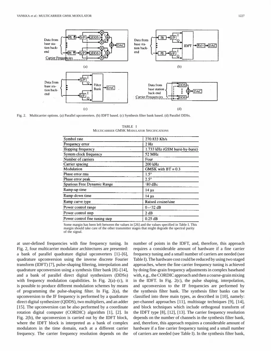
Fig. 2. Multicarrier options. (a) Parallel upconverters. (b) IDFT based. (c) Synthesis filter bank based. (d) Parallel DDSs.
TABLE IMULTICARRIER GMSK MODULATOR SPECIFICATIONS
Some margin has been left between the values in [26] and the values specified in Table I. Thismargin should take care of the other transmitter stages that might degrade the spectral purityof the signal.
at user-defined frequencies with fine frequency tuning. InFig. 2, four multicarrier modulator architectures are presented:a bank of parallel quadrature digital upconverters [1]–[6],quadrature upconversion using the inverse discrete Fouriertransform (IDFT) [7], pulse-shaping filtering, interpolation andquadrature upconversion using a synthesis filter bank [8]–[14],and a bank of parallel direct digital synthesizers (DDSs)with frequency modulation capabilities. In Fig. 2(a)–(c), itis possible to produce different modulation schemes by meansof programming the pulse-shaping filter. In Fig. 2(a), theupconversion to the IF frequency is performed by a quadraturedirect digital synthesizer (QDDS), two multipliers, and an adder[15]. The upconversion can be also performed by a coordinaterotation digital computer (CORDIC) algorithm [1], [2]. InFig. 2(b), the upconversion is carried out by the IDFT block,where the IDFT block is interpreted as a bank of complexmodulators in the time domain, each at a different carrierfrequency. The carrier frequency resolution depends on the
number of points in the IDFT, and, therefore, this approachrequires a considerable amount of hardware if a fine carrierfrequency tuning and a small number of carriers are needed (seeTable I). The hardware cost could be reduced by using two stagedapproaches, where the fine carrier frequency tuning is achievedby doing fine-grain frequency adjustments in complex basebandwith, e.g., the CORDIC approach and then a coarse-grain mixingin the IDFT. In Fig. 2(c), the pulse shaping, interpolation,and upconversion to the IF frequencies are performed bythe synthesis filter bank. The synthesis filter banks can beclassified into three main types, as described in [10], namely:per-channel approaches [11], multistage techniques [9], [14],and block techniques which include orthogonal transform ofthe IDFT type [8], [12], [13]. The carrier frequency resolutiondepends on the number of channels in the synthesis filter bank,and, therefore, this approach requires a considerable amount ofhardware if a fine carrier frequency tuning and a small numberof carriers are needed (see Table I). In the synthesis filter bank,

1228 IEEE JOURNAL OF SOLID-STATE CIRCUITS, VOL. 37, NO. 10, OCTOBER 2002
Fig. 3. Multicarrier GMSK modulator.
the carrier frequency resolution can be also improved by doingfine frequency adjustments in complex baseband [14]. Thefine carrier frequency resolution could be achieved with lowhardware cost in Fig. 2(a) and (d) by programming the QDDSor DDS [16]. The fine carrier frequency resolution gives a highdegree of flexibility in IF and RF frequency planning. TheGMSK modulation used in the GSM is frequency modulation.The frequency modulation and upconversion could be donedirectly by the DDS in Fig. 2(d) [16], saving hardware comparedwith the architectures in Fig. 2(a)–(c). Therefore, the choicewas made in favor of the DDS bank architecture with frequencymodulation capabilities.
III. GMSK M ODULATOR
The interface field-programmable gate array (FPGA) inFig. 3 extracts data bits, power-level indications, frequencycontrol words, initialization, and control data from the base-sta-tion back-end. The FPGA feeds necessary data and control bitsto the multicarrier GMSK modulator. The block diagram ofthe GMSK modulator is shown in Fig. 4. The system consistsof a shift register, counter, frequency trajectory look-up table(LUT), adder/subtractor, phase accumulator, carrier frequencyregister, phase-to-amplitude converter (conventionally, a sineROM) and D/A converter. The input data symbols are filteredby the Gaussian low-pass filter [17]. The use of the LUT as adigital filter has been described in [18] and [19]. Incoming datasymbols to the frequency trajectories LUT are stored in theshift register (see Fig. 4). The simulation shows that in order tomeet modulation spectrum requirements, the impulse responseof the Gaussian filter can be truncated to a 2-bit width (threestages in the shift register) [20]. Utilization of the redundancyin the stored waveforms reduces the size of the frequencytrajectories LUT to less than a quarter of the original size inthe modulator [20].
The output of the adder/subtractor is , whereis the carrier frequency (carrier offset) control word, is
the frequency modulation control word (the LUT output), andis the input to the phase accumulator,being the time index.
The phase value of the phase accumulator is, where is the phase accumulator width. The
phase accumulator acts as a digital integrator followed by amodulo operator. The output frequency is
(1)
where is the clock frequency. As the GMSK modulator gen-erates frequencies close to one half of the clock frequency, thefirst image becomes more difficult to filter. Therefore, the max-imum output frequency is limited to approximately 0.33 timesthe clock frequency. The input to the phase accumulatorcanonly have integer values, therefore, the frequency resolution isfound, setting , as
(2)
The frequency resolution will be 0.77 Hz from (2), when is52 MHz, and is 26. The frequency resolution is better than thetarget frequency error specification in Table I.
The number of samples per symbol is 192 (MHz MHz) in the frequency trajectories
LUT. The burst length is 156.25 bits in GSM systems [21]. Aquarter of a guard bit ( samples) is insertedafter each burst, following the eight differentially coded guardbit ones [21]. Therefore, the counter has 48/192 modes in Fig. 4[20].
The phase accumulator addresses the sine ROM, which con-verts the phase information into the values of a sine wave. A sinememory compression technique is applied to reduce the size andaccess time of the sine ROM [22]. The wordlengths of the com-pressed sine ROM are described in [20]. The multiplier controlsthe envelope of the digital GMSK modulated IF signal in Fig. 4.The four GMSK modulated signals are combined together in thedigital domain, as shown in Fig. 3. Next, the signal is presentedto the D/A converter, which develops an analog signal.
IV. RAMP GENERATOR AND OUTPUT POWER-LEVEL
CONTROLLER
A. Conventional Solutions
Multicarrier transmission with digital carrier combining ne-cessitates power control to be implemented in the digitaldomain. Otherwise, it would not be possible to adjust therelative power of a single carrier with respect to the others.Therefore, a digital ramp generator and output power-levelcontroller is proposed in Fig. 4.
Conventional methods for implementing the ramp generatorand output power controller are to use either a memory or afinite-impulse response (FIR) filter. The clock frequency is highin the digital IF modulators, therefore, the size of the necessarymemory is large. Furthermore, the multiplier is needed to set theoutput power level. Similarly, due to the high clock frequencyin the IF modulators, there are many taps in the FIR. Multistageimplementations may reduce the number of the taps to someextent.

VANKKA et al.: MULTICARRIER GMSK MODULATOR 1229
Fig. 4. Details of the single GMSK modulator and ramping unit in the multicarrier GMSK modulator (Fig. 3).
Fig. 5. Ramp generator and output power-level controller.
B. New Ramp Generator and Output Power-Level Controller
The power-control range of the proposed design is 0 to32 dB, where the 0-dB level is the nominal maximum power.
The downlink dynamic power control in GSM uses up to 16power levels with 2-dB separation (30 dB). The additional2-dB range is introduced to assist the gain stabilization ofthe transmitter analog parts. Furthermore, a power-controlfine-tuning step (0.25 dB) is introduced for this purpose (seeTable I). The power level can be changed burst by burst. Thedigital GMSK modulated IF signal is multiplied by the rampsignal for a smooth rise and fall of the burst in Fig. 4. Thepower control is realized by scaling the ramp curve, whichfollows a raised cosine/sine curve. The new ramp generator andoutput power-level controller is shown in Fig. 5. The output ofthe ramp generator and output power-level controller is
dc dc (3)
where dc determines the starting power level before the rampand the power level after the ramp [20],is the amplitude ofthe ramp, is , and is phase offset (0 for raised co-sine and for raised sine). It generates the raised sine for powerup and the raised cosine for power down. The valuecontrolsthe amplitude of the ramp (power level). The cosine term in(3) is implemented by a recursive digital sinusoidal oscillator inFig. 5. The value controls the amplitude of the ramp (powerlevel) [20]. During the ramp period the signal sel is low in Fig. 5and the multiplexer conducts the ramp signal to the multiplier(Fig. 4). After the ramp duration , the signal sel becomeshigh, the output of the multiplexer is connected to the inputof the multiplexer, and the output power level is constant. Thenumber of samples for power ramping up/power ramping down
Fig. 6. D/A converter system.
is , where is 52 MHz (see Table I) and is14 s from Table I. The details and finite wordlength effects ofthe digital ramp generator and output power-level controller aredescribed in [20].
The D/A converter usually exhibits a fully sample-and-holdoutput that causes the rolloff function to the spectrumof the converted analog signals. One method for compensatingfor the rolloff is the use of the inverse filter inthe IF frequency [23]. The digital ramp generator and outputpower-level controller can compensate for this droop, when thebandwidth of the single carrier is narrow. The rolloff istaken into account when the power-level value of the carrier iscalculated. There will be a slight slant in the D/A converter fre-quency response across the channel bandwidth of 200 kHz. Itwas calculated that with the maximum output carrier frequencyand D/A converter clock frequency (see Table I), the outputpower tilt across the channel bandwidth is 0.04 dB. The effecton the modulator performance can be considered negligible.
V. D/A CONVERTER
The 14-bit D/A converter is based on a segmentedcurrent steering architecture. It consists of a 6-bit ther-mometer-coded most-significant-bit (MSB) segment, a 3-bitthermometer-coded second segment, and a binary-coded 5-bitleast-significant-bit (LSB) segment. The dynamic linearity isof utmost importance in this multicarrier IF modulator becauseof the strongly varying envelope of the composite signal. Thestatic linearity, which is achieved by sizing the current sources

1230 IEEE JOURNAL OF SOLID-STATE CIRCUITS, VOL. 37, NO. 10, OCTOBER 2002
Fig. 7. MSB switch cell of the D/A converter and biasing.
for intrinsic matching [24], is a prerequisite for obtaining agood dynamic linearity. The maximum dynamic performanceis achieved by multiplexing two on-chip D/A converters withoutput sampling switches, which are transmission gates. TheD/A converter system, comprising two D/A converters that aresampled sequentially at half the clock rate, is shown in Fig. 6.For the output switches, the current transients are sampled tothe external dummy resistor load RD and settled current to theexternal output resistor loads RP and RN. As the output currentis sampled, the need to latch data inside the D/A convertersis reduced; the D/A converter structure is simplified and thedigital noise coupled to the analog output current is reduced. Ahigh-swing cascode current mirror is used to bias the currentsource transistors of the D/A converter (Fig. 7). This approachprovides a large voltage to the current source transistors,and, thus, improved matching between the current sources, dueto the decreased effect of the variation of. A 1.4-V supplyvoltage is regulated and stabilized internally for the digital partsof the D/A converter and for the high-swing current mirrors.The layout of D/A converters 1 and 2 consists of switch cells,latched thermometer coders, LSB latches, and input registers.
The measured integral nonlinearity (INL) and differentialnonlinearity (DNL) are 5 and 3 LSB, respectively. The INLand DNL were measured at the output of the two interleavedD/A converters and at the outputs of the separate D/A con-verters. The measurement results indicate that the matchingproblems inside the D/A converter dominate the static linearityerrors, not the matching between the two identical D/A con-verters. The INL and DNL performance can be improved byusing larger devices and in the current sources for bettermatching [25] and by using a single current-source transistormatrix containing both the interleaved D/A converters. How-ever, the dynamic nonlinearities dominate the output spectrumbecause of the strongly varying envelope of the compositesignal, not the static nonlinearities.
VI. CHIP DESIGN ISSUES
This multicarrier GSMK modulator was synthesized from thevery-high-speed integrated circuits hardware description lan-guage (VHDL) description using the 0.35-m CMOS standardcell library. Static timing check and prelayout timing simula-tions were performed for the netlist, and the chip layout was
Fig. 8. Chip micrograph.
completed using place and route tools. Finally, based on the par-asitic information extracted from the layout, the post-layout de-lays were back annotated to timing verification. Fig. 8 displaysthe chip micrograph.
The multicarrier GMSK modulator is a mixed-signal high-precision monolithic device, which requires a significant designeffort at the physical level. The D/A converter is implementedwith a differential design, which results in reduced even-orderharmonics and provides common-mode rejection to distur-bances. In order to minimize the coupling of the switchingnoise from the digital logic to the analog output, on-chipdecoupling capacitors (total capacitance of 2 nF) are used toreduce the ground bounce in the digital part. In the BiCMOStechnology used, transistors can be easily isolated in the epilayer, which is an effective way to eliminate substrate cou-pling. Interference at the on-chip D/A converter output bandis reduced, avoiding digital hardware using in-band clock fre-quencies (frequency planning).
VII. M EASUREMENTRESULTS
The spectrum due to the modulation and wide-band noisein the cases of single-carrier and multicarrier transmissions isshown in Fig. 9, where the dashed line shows the spectrumrequirements due to the GMSK modulation. Some margin(6 dB) has been left between the most stringent modulationspectrum requirement defined for GSM microcell base stationsin [26] and the values specified in Fig. 9 at offsets larger than

VANKKA et al.: MULTICARRIER GMSK MODULATOR 1231
Fig. 9. Measured GSM base-station spectrum due to GMSK modulation(single carrier, multicarrier) in the D/A converter input.
Fig. 10. Measured phase and frequency errors.
1800 kHz. This is because in the case of the multicarrier digitalmodulator it is not possible to use steep analog bandpassfilters [Fig. 1(b)] around each carrier. After the four carriersare combined together in Fig. 3, the power per carrier is notchanged, but the noise floor is increased by 6 dB. Therefore,when compared to single-carrier transmission, the noise floor isabout 6 dB higher in case of multicarrier transmission in Fig. 9.Increasing the wordlengths of the sine ROM and the multiplierand changing the quantization to be done after the carriercombining could reduce this degradation. In the GMSK IFmodulator, most of the errors are generated less by quantizationerrors in the digital domain and more by the D/A converteranalog nonidealities. Hence, the spectral improvement inthe digital output would not be visible in the D/A converterIF output. The wordlengths used are sufficient to fulfill thetarget spectrum requirements due to the modulation, as shownin Fig. 9. The increased wordlengths of the multipliers andsine ROMs would add complexity and enlarge the core area.Therefore, it was decided that the wordlengths shown in Figs. 3and 4 should be used. The wordlengths were selected fromsystem simulation [16], [20].
The phase-error target is specified to be 1.5root mean square(rms) with a peak value of 2.5, and the target frequency error is2 Hz (see Table I). The measured rms phase error is 1.04witha maximum peak deviation 2.1, and a peak frequency error of
1.2 Hz at the D/A converter output (see Fig. 10).
Fig. 11. Measured transmitted power level of the burst versus time. Observethat the middle part of the burst is not shown.
Fig. 12. Measured power spectrum of the modulated carrier.
Fig. 11 shows the measured ramp-up and ramp-down profilesof the transmitted burst, which satisfy the GSM base-stationpower versus time masks. The allowed power of spuriousresponses originating from the power ramping before andafter the bursts are specified by the switching transient limits.Some margin (3 dB) has been left between the values in [26]and the values specified for this implementation in Table IIto take care of the other transmitter stages that might degradethe spectral purity of the signal. The power levels measured atthe digital output are well below the limits shown in Table II,while the power levels measured at the D/A converter outputcannot conform to the target requirements due to the dynamicrange limitations of the D/A converter.

1232 IEEE JOURNAL OF SOLID-STATE CIRCUITS, VOL. 37, NO. 10, OCTOBER 2002
TABLE IISPECTRUM DUE TOSWITCHING TRANSIENTS(PEAK-HOLD MEASUREMENT, 30KHZ FILTER BANDWIDTH, REFERENCE� 300 kHz WITH ZEROOFFSET)
Fig. 13. Measured four carriers. (a) At maximum dynamic power level. (b) With different power levels (relative power-level difference is 10 dB). (c) One is 32 dBbelow the others.
The single carrier in Fig. 12 fulfills the modulation spectrumrequirements for microcell base stations [26]. Fig. 13(a) showsthe multicarrier output, where all carriers are at maximum dy-namic power level. Fig. 13(b) and (c) shows carriers with dif-ferent power levels. The problem with a digital ramp generatorand output power-level controller is the reduced carrier-to-noise
ratio at low dynamic power-control levels because the dy-namic power control is realized by scaling in the digital domain.
However, according to the specification, the modulation spec-trum is measured only at the maximum dynamic power-controllevel [26] and, hence, the reduced ratio at low power-con-trol levels does not present a problem in meeting the specifi-cations. The effect of the ratio degradation on the inbandsignal quality is negligible, since even at the lowest dynamicpower-control level, the relative noise power is small enoughnot to affect signal quality.

VANKKA et al.: MULTICARRIER GMSK MODULATOR 1233
VIII. C ONCLUSION
The multicarrier GMSK modulator with a 14-bit on-chipD/A converter is presented. The digital modulator fulfills spec-trum and phase-error specifications for GSM 900/1800/1900base stations for pico-, micro-, and macrocells. The switchingtransients power levels and power spectra measured at the D/Aconverter output cannot conform to the target requirementsdue to the dynamic range limitations of the D/A converter.The new digital ramp generator and output power-level con-troller performs both the burst ramping and the dynamic powercontrol in the digital domain. The maximum dynamic perfor-mance is obtained by multiplexing two D/A converters withoutput sampling switches. The major limiting factor of digitalIF multicarrier modulator performance at base-station appli-cations is the D/A converter, because the development of D/Aconverters does not keep up with the capabilities of digitalsignal processing with faster technologies. The die area of thechip is 26.8 mm in 0.35- m CMOS (in BiCMOS) technology.Power consumption is 706 mW at 3.3 V with 52 MHz.
ACKNOWLEDGMENT
The authors appreciate the comments and suggestions of thereviewers.
REFERENCES
[1] J. Vankka, M. Kosunen, I. Sanchis, and K. Halonen, “A multicarrierQAM modulator,”IEEE Trans. Circuits Syst. II, vol. 47, pp. 1–10, Jan.2000.
[2] M. Kosunen, J. Vankka, M. Waltari, and K. Halonen, “A multicarrierQAM modulator for WCDMA basestation with on-chip D/A converter,”in Proc. IEEE Custom Integrated Circuits Conf., San Diego, CA, May2001, pp. 301–304.
[3] J. Vankka, J. Ketola, O. Väänänen, J. Sommarek, M. Kosunen, and K.Halonen, “A GSM/EDGE/WCDMA modulator with on-chip D/A con-verter for base station,”IEEE Int. Solid-State Circuits Conf. Dig. Tech.Papers, pp. 236–237, Feb. 2002.
[4] “ISL5217 Quad Programmable UpConverter Data Sheet,” Intersil Cor-poration, Irvine, CA, 2001.
[5] “AD6623 Four Channel, 104 MSPS Digital Transmit Signal Processor(TSP), Preliminary Technical Data Sheet,” Analog Devices, Norwood,MA, 2001.
[6] “GC4116 Multi-Standard Quad DUC Chip Data Sheet,” Graychip, Inc.,Palo Alto, CA, 2001.
[7] N. Weste and D. J. Skellern, “VLSI for OFDM,”IEEE Commun. Mag.,vol. 36, pp. 127–131, Oct. 1998.
[8] M. G. Bellanger and J. L. Daguet, “TDM-FDM transmultiplexer:Digital polyphase and FFT,”IEEE Trans. Commun., vol. COM-22, pp.1199–1204, Sept. 1974.
[9] T. Tsuda, S. Morita, and Y. Fujii, “Digital TDM-FDM translatorwith multistage structure,”IEEE Trans. Commun., vol. COM-26, pp.734–741, May 1978.
[10] H. Scheuermann and H. Göckler, “A comprehensive survey of digitaltransmultiplexing methods,”Proc. IEEE, vol. 69, pp. 1419–1450, Nov.1981.
[11] C. F. Kurth, K. J. Bures, P. R. Gagnon, and M. H. Etzel, “A per-channel,memory-oriented transmultiplexer with logarithmic processing,”IEEETrans. Commun., vol. COM-30, pp. 1520–1527, July 1982.
[12] I. R. Corden and R. A. Carrasco, “Fast transform based complextransmultiplexer algorithm for multiband quadrature digital modulationschemes,”Proc. Inst. Elect. Eng., pt. 1, vol. 137, no. 6, pp. 408–416,Dec. 1990.
[13] S. Im, W. Lee, C. Kim, Y. Shin, S. H. Lee, and J. Chung, “Imple-mentation of SDR-based digital IF channelizer/de-channelizer formultiple CDMA signals,”IEICE Trans. Commun., vol. E83-B, no. 6,pp. 1282–1289, June 2000.
[14] R. Pasko, L. Rijnders, P. R. Schaumont, S. A. Vernalde, and D.Duracková, “High-performance flexible all-digital quadrature upand down converter chip,”IEEE J. Solid-State Circuits, vol. 36, pp.408–416, Mar. 2001.
[15] K. H. Cho and H. Samueli, “A frequency-agile single-chip QAM modu-lator with beamforming diversity,”IEEE J. Solid-State Circuits, vol. 36,pp. 398–407, Mar. 2001.
[16] J. Vankka and K. Halonen,Direct Digital Synthesizers: Theory, Designand Applications. Norwell, MA: Kluwer, 2001.
[17] Modulation, GSM Recommendation 05.04, 1999.[18] N. Boutin, C. Porlier, and S. Morissette, “A digital filter-modulation
combination for data transmission,”IEEE Trans. Commun., vol.COM-25, pp. 1242–1244, Oct. 1977.
[19] A. Linz and A. Hendrickson, “Efficient implementation of anI–QGMSK modulator,”IEEE Trans. Circuits Syst. II, vol. 43, pp. 14–23,Jan. 1996.
[20] J. Vankka, M. Honkanen, and K. Halonen, “A multicarrier GMSK mod-ulator,” IEEE J. Select. Areas Commun., vol. 19, pp. 1070–1079, June2001.
[21] Digital Cellular Telecommunications System (Phase 2+); Radio Sub-system Synchronization, GSM Recommendation 05.10, 1999.
[22] L. K. Tan and H. Samueli, “A 200-MHz quadrature digital synthe-sizer/mixer in 0.8-�m CMOS,” IEEE J. Solid-State Circuits, vol. 30,pp. 193–200, Mar. 1995.
[23] H. Samueli, “The design of multiplierless FIR filters for compensatingD/A converter frequency response distortion,”IEEE Trans. CircuitsSyst., vol. 35, pp. 1064–1066, Aug. 1988.
[24] A. Van den Bosch, M. A. F. Borremans, M. S. J. Steyaert, and W. Sansen,“A 10-bit 1-Gsample/s Nyquist current-steering CMOS D/A converter,”IEEE J. Solid-State Circuits, vol. 36, pp. 315–324, Mar. 2001.
[25] M. Pelgrom, A. Duinmaijer, and A. Webers, “Matching properties ofMOS transistors,”IEEE J. Solid-State Circuits, vol. 24, pp. 1433–1440,Oct. 1989.
[26] Radio Transmission and Reception, GSM Recommendation 05.05,1999.
Jouko Vankka (S’96) was born in Helsinki, Finland,in 1965. He received the M.S. degree in electricalengineering from Helsinki University of Technology(HUT) in 1991. Since 1995, he has been workingtoward the Ph.D. degree as a Research Scientist atthe Electronic Circuit Design Laboratory, HUT.
His research interests include VLSI architecturesand mixed-signal integrated circuits for communica-tion applications.
Jaakko Pyykönen(M’01) received the M.Sc degreein electronic engineering from Helsinki University ofTechnology (HUT), Helsinki, Finland, in 1994.
From 1993 to 1995, he was with the ElectronicCircuit Design Laboratory, HUT. After working withAtmel Finland Development Center OY (formerlyFincitec Components OY) from 1995 to 1998,he joined Nokia Research Center, Helsinki. Hisresearch interests are in the area of analog andmixed-signal functions.
Johan Sommarekwas born in Kervo, Finland, in1974. He received the M.Sc degree from HelsinkiUniversity of Technology (HUT), Helsinki, Fin-land, in 2000. He is currently working toward theD.Sc. degree in electrical and telecommunicationsengineering at HUT.
His research interest are in the areas of VLSI forsignal processing in telecommunications and high-speed CMOS integrated circuit design.

1234 IEEE JOURNAL OF SOLID-STATE CIRCUITS, VOL. 37, NO. 10, OCTOBER 2002
Mauri Honkanen was born in Pori, Finland, onAugust 9, 1969. He received the M.Sc degree (withhonors) in electrical engineering from HelsinkiUniversity of Technology (HUT), Espoo, Finland, in1995.
From 1994 to 1995, he was a Research Assistantwith the Communications Laboratory, HUT, per-forming research on radio propagation modelingwith ray tracing. From 1996 to 1997, he investigatedsystem modeling of RF components as a ResearchScientist at HUT. In 1998, he joined Nokia Research
Center, Tampere, Finland, to work on transceiver system design as a ResearchEngineer, and since 2000 as a Senior Research Engineer. Recently, he hasalso been involved in system design of wireless personal area networks. Hiscurrent research interests are transceiver architectures, RF system modelingand simulation, and short-range wireless communication systems.
Kari A. I. Halonen was born in Helsinki, Finland, onMay 23, 1958. He received the M.S. degree in elec-trical engineering from Helsinki University of Tech-nology (HUT) in 1982, and the Ph.D. degree in elec-trical engineering from the Katholieke UniversiteitLeuven, Heverlee, Belgium, in 1987.
From 1982 to 1984, he was with HUT as an Assis-tant and with the Technical Research Center of Fin-land as a Research Assistant. From 1984 to 1987, hewas a Research Assistant with the E.S.A.T. Labora-tory, Katholieke Universiteit Leuven, with a tempo-
rary grant from the Academy of Finland. Since 1988, he has been with theElectronic Circuit Design Laboratory, HUT, as a Senior Assistant from 1988to 1990, and as the Director of the Integrated Circuit Design Unit of the Micro-electronics Center from 1990 to 1993. He was on leave of absence the academicyear 1992–1993, acting as Research and Development Manager with FincitecInc., Finland. From 1993 to 1996, he was an Associate Professor, and since1997, a full Professor with the Faculty of Electrical Engineering and Telecom-munications, HUT. He is the author or coauthor of 100 international and nationalconference and journal publications on analog integrated circuits. His researchinterests are in CMOS and BiCMOS analog integrated circuits, particularly fortelecommunication applications.