a monolithic fully-integrated vacuum-sealed cmos pressure sensor
TRANSCRIPT
164 IEEE TRANSACTIONS ON ELECTRON DEVICES, VOL. 49, NO. 1, JANUARY 2002
A Monolithic Fully-Integrated Vacuum-SealedCMOS Pressure Sensor
Abhijeet V. Chavan, Senior Member, IEEE,and Kensall D. Wise, Fellow, IEEE
Abstract—This paper presents an integrated multi-transducercapacitive barometric pressure sensor that is vacuum-sealed atwafer level. The interface circuitry is integrated directly withinthe sealed reference cavity, making the device immune to par-asitic environmental effects. The overall device process mergesBiCMOS circuitry with a dissolved-wafer transducer process andis compatible with bulk- and surface-micromachined transducers.The process employs chemical-mechanical polishing (CMP),anodic bonding, and hermetic lead transfers. The sensor achieves25 mTorr resolution and is suitable for low-cost packaging. It iscomposed of a programmable switched-capacitor (SC) readoutcircuit, five segmented-range pressure transducers, and a refer-ence capacitor, all integrated on a6 5 7 5 mm2 die using 3- mfeatures.
Index Terms—Capacitive, CMOS readout, integrated sensors,MEMS, monolithic, pressure, vacuum sealing.
I. INTRODUCTION
T HE DEVELOPMENT of integrated sensors containingon-chip interface circuitry has become a primary focus
in MEMS in order to achieve improved performance, reducedcost, and realization of the system-on-chip concept. Suchsensors reduce the effects of parasitics and external interfer-ence because the signal is amplified in close proximity to thetransducer; however, they also pose interesting challenges inmerging transducer and circuit processes, maintaining testa-bility, and achieving reliable vacuum encapsulation. Vacuumencapsulation is required in many devices to eliminate problemsrelating to temperature-induced gas expansion, squeeze-filmdamping, and stiction during final release of the device. Inaddition, the availability of an assembly-ready device cansignificantly reduce packaging costs associated with hermeticsealing and permit injection-molded plastic packaging to beused. The die area required for a sensor having embeddedreadout circuitry is typically smaller than for two separatedies as used in hybrid integration, and any reliability problemsassociated with inter-chip interconnects are eliminated.
Manuscript received April 16, 2001; revised August 16, 2001. This work wassupported in part by the Defense Advanced Research Projects Agency underContract DABT63-C-0111. The review of this paper was arranged by Editor K.Najafi.
A. V. Chavan is with Delphi Microelectronics Center, Delphi Delco Elec-tronic Systems Corporation, Kokomo, IN 46902 USA and also with with theCenter for Wireless Integrated MicroSystems, Department of Electrical Engi-neering and Computer Science, The University of Michigan, Ann Arbor, MI48109-2122 USA.
K. D. Wise is with the Center for Wireless Integrated MicroSystems,Department of Electrical Engineering and Computer Science, The Universityof Michigan, Ann Arbor, MI 48109-2122 USA and also with Delphi Micro-electronics Center, Delphi Delco Electronic Systems Corporation, Kokomo, IN46902 USA.
Publisher Item Identifier S 0018-9383(02)00235-6.
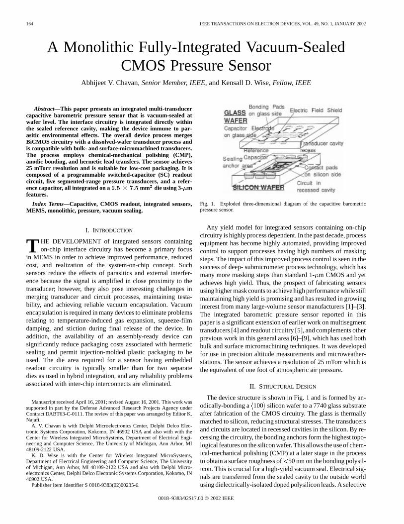
Fig. 1. Exploded three-dimensional diagram of the capacitive barometricpressure sensor.
Any yield model for integrated sensors containing on-chipcircuitry is highly process dependent. In the past decade, processequipment has become highly automated, providing improvedcontrol to support processes having high numbers of maskingsteps. The impact of this improved process control is seen in thesuccess of deep- submicrometer process technology, which hasmany more masking steps than standard 1-m CMOS and yetachieves high yield. Thus, the prospect of fabricating sensorsusing higher mask counts to achieve high performance while stillmaintaining high yield is promising and has resulted in growinginterest from many large-volume sensor manufacturers [1]–[3].The integrated barometric pressure sensor reported in thispaper is a significant extension of earlier work on multisegmenttransducers [4] and readout circuitry [5], and complements otherprevious work in this general area [6]–[9], which has used bothbulk and surface micromachining techniques. It was developedfor use in precision altitude measurements and microweather-stations. The sensor achieves a resolution of 25 mTorr which isthe equivalent of one foot of atmospheric air pressure.
II. STRUCTURAL DESIGN
The device structure is shown in Fig. 1 and is formed by an-odically-bonding a100 silicon wafer to a 7740 glass substrateafter fabrication of the CMOS circuitry. The glass is thermallymatched to silicon, reducing structural stresses. The transducersand circuits are located in recessed cavities in the silicon. By re-cessing the circuitry, the bonding anchors form the highest topo-logical features on the silicon wafer. This allows the use of chem-ical-mechanical polishing (CMP) at a later stage in the processto obtain a surface roughness of50 nm on the bonding polysil-icon. This is crucial for a high-yield vacuum seal. Electrical sig-nals are transferred from the sealed cavity to the outside worldusing dielectrically-isolated doped polysilicon leads. A selective
0018–9383/02$17.00 © 2002 IEEE
CHAVAN AND WISE: MONOLITHIC FULLY-INTEGRATED VACUUM-SEALED CMOS 165
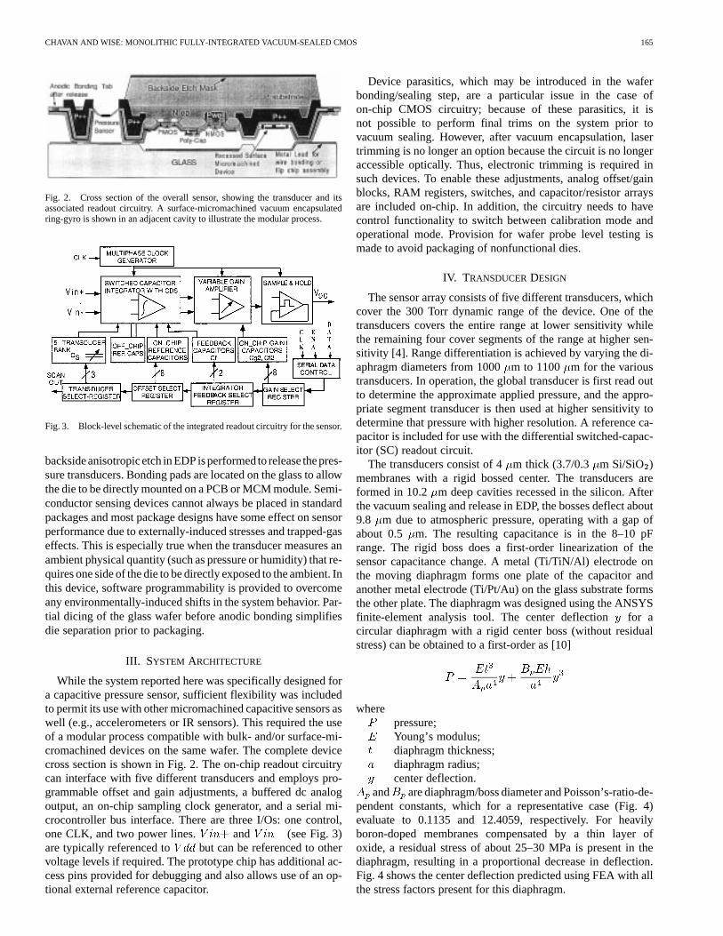
Fig. 2. Cross section of the overall sensor, showing the transducer and itsassociated readout circuitry. A surface-micromachined vacuum encapsulatedring-gyro is shown in an adjacent cavity to illustrate the modular process.
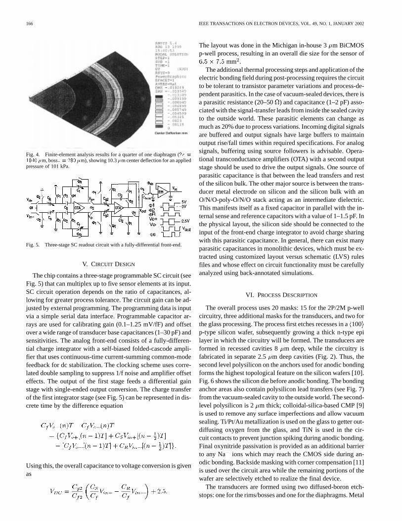
Fig. 3. Block-level schematic of the integrated readout circuitry for the sensor.
backsideanisotropicetch inEDP isperformed to release thepres-sure transducers. Bonding pads are located on the glass to allowthe die to be directly mounted on a PCB or MCM module. Semi-conductor sensing devices cannot always be placed in standardpackages and most package designs have some effect on sensorperformance due to externally-induced stresses and trapped-gaseffects. This is especially true when the transducer measures anambient physical quantity (such as pressure or humidity) that re-quires one side of the die to be directly exposed to the ambient. Inthis device, software programmability is provided to overcomeany environmentally-induced shifts in the system behavior. Par-tial dicing of the glass wafer before anodic bonding simplifiesdie separation prior to packaging.
III. SYSTEM ARCHITECTURE
While the system reported here was specifically designed fora capacitive pressure sensor, sufficient flexibility was includedto permit its use with other micromachined capacitive sensors aswell (e.g., accelerometers or IR sensors). This required the useof a modular process compatible with bulk- and/or surface-mi-cromachined devices on the same wafer. The complete devicecross section is shown in Fig. 2. The on-chip readout circuitrycan interface with five different transducers and employs pro-grammable offset and gain adjustments, a buffered dc analogoutput, an on-chip sampling clock generator, and a serial mi-crocontroller bus interface. There are three I/Os: one control,one CLK, and two power lines. and (see Fig. 3)are typically referenced to but can be referenced to othervoltage levels if required. The prototype chip has additional ac-cess pins provided for debugging and also allows use of an op-tional external reference capacitor.
Device parasitics, which may be introduced in the waferbonding/sealing step, are a particular issue in the case ofon-chip CMOS circuitry; because of these parasitics, it isnot possible to perform final trims on the system prior tovacuum sealing. However, after vacuum encapsulation, lasertrimming is no longer an option because the circuit is no longeraccessible optically. Thus, electronic trimming is required insuch devices. To enable these adjustments, analog offset/gainblocks, RAM registers, switches, and capacitor/resistor arraysare included on-chip. In addition, the circuitry needs to havecontrol functionality to switch between calibration mode andoperational mode. Provision for wafer probe level testing ismade to avoid packaging of nonfunctional dies.
IV. TRANSDUCERDESIGN
The sensor array consists of five different transducers, whichcover the 300 Torr dynamic range of the device. One of thetransducers covers the entire range at lower sensitivity whilethe remaining four cover segments of the range at higher sen-sitivity [4]. Range differentiation is achieved by varying the di-aphragm diameters from 1000m to 1100 m for the varioustransducers. In operation, the global transducer is first read outto determine the approximate applied pressure, and the appro-priate segment transducer is then used at higher sensitivity todetermine that pressure with higher resolution. A reference ca-pacitor is included for use with the differential switched-capac-itor (SC) readout circuit.
The transducers consist of 4m thick (3.7/0.3 m Si/SiO )membranes with a rigid bossed center. The transducers areformed in 10.2 m deep cavities recessed in the silicon. Afterthe vacuum sealing and release in EDP, the bosses deflect about9.8 m due to atmospheric pressure, operating with a gap ofabout 0.5 m. The resulting capacitance is in the 8–10 pFrange. The rigid boss does a first-order linearization of thesensor capacitance change. A metal (Ti/TiN/Al) electrode onthe moving diaphragm forms one plate of the capacitor andanother metal electrode (Ti/Pt/Au) on the glass substrate formsthe other plate. The diaphragm was designed using the ANSYSfinite-element analysis tool. The center deflectionfor acircular diaphragm with a rigid center boss (without residualstress) can be obtained to a first-order as [10]
wherepressure;Young’s modulus;diaphragm thickness;diaphragm radius;center deflection.
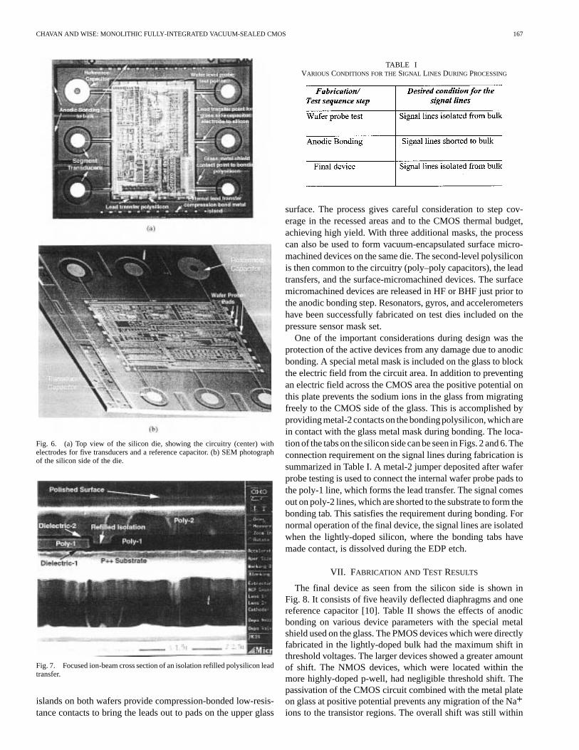
and are diaphragm/boss diameter and Poisson’s-ratio-de-pendent constants, which for a representative case (Fig. 4)evaluate to 0.1135 and 12.4059, respectively. For heavilyboron-doped membranes compensated by a thin layer ofoxide, a residual stress of about 25–30 MPa is present in thediaphragm, resulting in a proportional decrease in deflection.Fig. 4 shows the center deflection predicted using FEA with allthe stress factors present for this diaphragm.
166 IEEE TRANSACTIONS ON ELECTRON DEVICES, VOL. 49, NO. 1, JANUARY 2002
Fig. 4. Finite-element analysis results for a quarter of one diaphragm (2r =
1040 �m, boss = 280 �m), showing 10.3�m center deflection for an appliedpressure of 101 kPa.
Fig. 5. Three-stage SC readout circuit with a fully-differential front-end.
V. CIRCUIT DESIGN
The chip contains a three-stage programmable SC circuit (seeFig. 5) that can multiplex up to five sensor elements at its input.SC circuit operation depends on the ratio of capacitances, al-lowing for greater process tolerance. The circuit gain can be ad-justed by external programming. The programming data is inputvia a simple serial data interface. Programmable capacitor ar-rays are used for calibrating gain (0.1–1.25 mV/fF) and offsetover a wide range of transducer base capacitances (1–30 pF) andsensitivities. The analog front-end consists of a fully-differen-tial charge integrator with a self-biased folded-cascode ampli-fier that uses continuous-time current-summing common-modefeedback for dc stabilization. The clocking scheme uses corre-lated double sampling to suppress 1/f noise and amplifier offseteffects. The output of the first stage feeds a differential gainstage with single-ended output conversion. The charge transferof the first integrator stage (see Fig. 5) can be represented in dis-crete time by the difference equation
Using this, the overall capacitance to voltage conversion is givenas
The layout was done in the Michigan in-house 3m BiCMOSp-well process, resulting in an overall die size for the sensor of
mm .The additional thermal processing steps and application of the
electric bonding field during post-processing requires the circuitto be tolerant to transistor parameter variations and process-de-pendent parasitics. In the case of vacuum-sealed devices, there isa parasitic resistance (20–50) and capacitance (1–2 pF) asso-ciated with the signal-transfer leads from inside the sealed cavityto the outside world. These parasitic elements can change asmuch as 20% due to process variations. Incoming digital signalsare buffered and output signals have large buffers to maintainoutput rise/fall times within required specifications. For analogsignals, buffering using source followers is advisable. Opera-tional transconductance amplifiers (OTA) with a second outputstage should be used to drive the output signals. One source ofparasitic capacitance is that between the lead transfers and restof the silicon bulk. The other major source is between the trans-ducer metal electrode on silicon and the silicon bulk with anO/N/O-poly-O/N/O stack acting as an intermediate dielectric.This manifests itself as a fixed capacitor in parallel with the in-ternal sense and reference capacitors with a value of 1–1.5 pF. Inthe physical layout, the silicon side should be connected to theinput of the front-end charge integrator to avoid charge sharingwith this parasitic capacitance. In general, there can exist manyparasitic capacitances in monolithic devices, which must be ex-tracted using customized layout versus schematic (LVS) rulesfiles and whose effect on circuit functionality must be carefullyanalyzed using back-annotated simulations.
VI. PROCESSDESCRIPTION
The overall process uses 20 masks: 15 for the 2P/2M p-wellcircuitry, three additional masks for the transducers, and two forthe glass processing. The process first etches recesses in a100p-type silicon wafer, subsequently growing a thick n-type epilayer in which the circuitry will be formed. The transducers areformed in recessed cavities 8m deep, while the circuitry isfabricated in separate 2.5m deep cavities (Fig. 2). Thus, thesecond level polysilicon on the anchors used for anodic bondingforms the highest topological feature on the silicon wafers [10].Fig. 6 shows the silicon die before anodic bonding. The bondinganchor areas also contain polysilicon lead transfers (see Fig. 7)from the vacuum-sealed cavity to the outside world. The second-level polysilicon is 2 m thick; colloidal-silica-based CMP [9]is used to remove any surface imperfections and allow vacuumsealing. Ti/Pt/Au metallization is used on the glass to getter out-diffusing oxygen from the glass, and TiN is used in the cir-cuit contacts to prevent junction spiking during anodic bonding.Final oxynitride passivation is provided as an additional barrierto any Na ions which may reach the CMOS side during an-odic bonding. Backside masking with corner compensation [11]is used over the circuit area while the remaining portions of thewafer are selectively etched to realize the final device.
The transducers are formed using two diffused-boron etch-stops: one for the rims/bosses and one for the diaphragms. Metal
CHAVAN AND WISE: MONOLITHIC FULLY-INTEGRATED VACUUM-SEALED CMOS 167
Fig. 6. (a) Top view of the silicon die, showing the circuitry (center) withelectrodes for five transducers and a reference capacitor. (b) SEM photographof the silicon side of the die.
Fig. 7. Focused ion-beam cross section of an isolation refilled polysilicon leadtransfer.
islands on both wafers provide compression-bonded low-resis-tance contacts to bring the leads out to pads on the upper glass
TABLE IVARIOUS CONDITIONS FOR THESIGNAL LINES DURING PROCESSING
surface. The process gives careful consideration to step cov-erage in the recessed areas and to the CMOS thermal budget,achieving high yield. With three additional masks, the processcan also be used to form vacuum-encapsulated surface micro-machined devices on the same die. The second-level polysiliconis then common to the circuitry (poly–poly capacitors), the leadtransfers, and the surface-micromachined devices. The surfacemicromachined devices are released in HF or BHF just prior tothe anodic bonding step. Resonators, gyros, and accelerometershave been successfully fabricated on test dies included on thepressure sensor mask set.
One of the important considerations during design was theprotection of the active devices from any damage due to anodicbonding. A special metal mask is included on the glass to blockthe electric field from the circuit area. In addition to preventingan electric field across the CMOS area the positive potential onthis plate prevents the sodium ions in the glass from migratingfreely to the CMOS side of the glass. This is accomplished byproviding metal-2 contacts on the bonding polysilicon, which arein contact with the glass metal mask during bonding. The loca-tion of the tabs on the silicon side can be seen in Figs. 2 and 6. Theconnection requirement on the signal lines during fabrication issummarized in Table I. A metal-2 jumper deposited after waferprobe testing is used to connect the internal wafer probe pads tothe poly-1 line, which forms the lead transfer. The signal comesout on poly-2 lines, which are shorted to the substrate to form thebonding tab. This satisfies the requirement during bonding. Fornormal operation of the final device, the signal lines are isolatedwhen the lightly-doped silicon, where the bonding tabs havemade contact, is dissolved during the EDP etch.
VII. FABRICATION AND TEST RESULTS
The final device as seen from the silicon side is shown inFig. 8. It consists of five heavily deflected diaphragms and onereference capacitor [10]. Table II shows the effects of anodicbonding on various device parameters with the special metalshield used on the glass. The PMOS devices which were directlyfabricated in the lightly-doped bulk had the maximum shift inthreshold voltages. The larger devices showed a greater amountof shift. The NMOS devices, which were located within themore highly-doped p-well, had negligible threshold shift. Thepassivation of the CMOS circuit combined with the metal plateon glass at positive potential prevents any migration of the Naions to the transistor regions. The overall shift was still within
168 IEEE TRANSACTIONS ON ELECTRON DEVICES, VOL. 49, NO. 1, JANUARY 2002
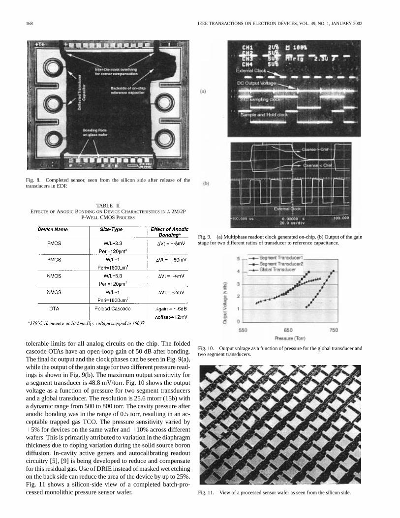
Fig. 8. Completed sensor, seen from the silicon side after release of thetransducers in EDP.
TABLE IIEFFECTS OFANODIC BONDING ON DEVICE CHARACTERISTICS IN A 2M/2P
P-WELL CMOS PROCESS
tolerable limits for all analog circuits on the chip. The foldedcascode OTAs have an open-loop gain of 50 dB after bonding.The final dc output and the clock phases can be seen in Fig. 9(a),while the output of the gain stage for two different pressure read-ings is shown in Fig. 9(b). The maximum output sensitivity fora segment transducer is 48.8 mV/torr. Fig. 10 shows the outputvoltage as a function of pressure for two segment transducersand a global transducer. The resolution is 25.6 mtorr (15b) witha dynamic range from 500 to 800 torr. The cavity pressure afteranodic bonding was in the range of 0.5 torr, resulting in an ac-ceptable trapped gas TCO. The pressure sensitivity varied by
5% for devices on the same wafer and10% across differentwafers. This is primarily attributed to variation in the diaphragmthickness due to doping variation during the solid source borondiffusion. In-cavity active getters and autocalibrating readoutcircuitry [5], [9] is being developed to reduce and compensatefor this residual gas. Use of DRIE instead of masked wet etchingon the back side can reduce the area of the device by up to 25%.Fig. 11 shows a silicon-side view of a completed batch-pro-cessed monolithic pressure sensor wafer.
Fig. 9. (a) Multiphase readout clock generated on-chip. (b) Output of the gainstage for two different ratios of transducer to reference capacitance.
Fig. 10. Output voltage as a function of pressure for the global transducer andtwo segment transducers.
Fig. 11. View of a processed sensor wafer as seen from the silicon side.
CHAVAN AND WISE: MONOLITHIC FULLY-INTEGRATED VACUUM-SEALED CMOS 169
VIII. C ONCLUSION
A monolithically integrated vacuum-sealed active pressuresensor was successfully fabricated using a monolithic CMOSmicromachining process. The test results show that noise in-terference levels from external factors can be substantially re-duced using this technique, giving a resolution of 25.6 mtorrover a dynamic range of 500–800 torr. The device makes useof vacuum encapsulation at wafer level, thereby significantlyreducing the packaging challenges. The process lends itself tobatch fabrication with minimal modification to a simple 3mCMOS process. Using the modular capability of the process,vacuum encapsulated surface-micromachined devices can alsobe fabricated in the same process flow.
REFERENCES
[1] T. Scheiter, H. Kapels, K. G. Oppermann, M. Steger, C. Hierold, W. M.Werner, and H. J. Timme, “Full integration of a pressure-sensor systeminto a standard BiCMOS process,”Sens. Actuators A, Phys., vol. A 67,pp. 211–214, 1998.
[2] X. Ding, W. Czarnocki, J. Schuster, and B. Roeckner, “DSP-basedCMOS monolithic pressure sensor for high volume manufacturing,”in Dig. Int. Conf. Solid-State Sensors and Actuators, June 1999, pp.362–365.
[3] H. J. Kress, J. Marek, M. Mast, O. Schatz, and J. Muchow,“Integrated silicon pressure sensor for automotive application withelectronic trimming,” inSAE Int. Congress and Exposition, Detroit,MI, Feb. 1995.
[4] A. V. Chavan and K. D. Wise, “A batch-processed vacuum-sealedcapacitive pressure sensor,” inIEEE Dig. Int. Conf. Solid-StateSensors and Actuators (Transducers), Chicago, June 1997, pp.1449–1452.
[5] A. V. Chavan, A. Mason, U. Kang, and K. D. Wise, “A programmablemixed-voltage sensor readout circuit and bus interface with built-inself-test,” in IEEE Dig. Int. Solid-State Circuits Conf., Feb. 1999, pp.136–137.
[6] M. Esashi, Y. Matsumoto, and S. Shoji, “Absolute pressure sensors byair-tight electrical feedthrough structure,”Sens. Actuators A, Phys., vol.A21-23, pp. 1048–1052, 1990.
[7] Y. Gianchandani, K. Ma, and K. Najafi, “A CMOS dissolved-waferprocess for integrated p++microelectromechanical systems,” inProc.Transducers, 1995, pp. 79–82.
[8] O. Paul and H. Baltes, “Novel fully CMOS-compatible vacuum sensor,”Sens. Actuators A, Phys., vol. A 46-47, pp. 143–146, 1995.
[9] E. Spigel, M. Kandler, Y. Manoli, and W. Mokwa, “A CMOS sensorand signal conversion chip for monitoring arterial blood pressures andtemperatures,” inProc. IEEE Int. Conf. Solid-State Circuits, 1992, pp.126–127.
[10] A. V. Chavan, “An integrated high-resolution capacitive barometricpressure sensing system,” Ph.D. dissertation, Univ. Michigan, AnnArbor, 1999.
[11] H. L. Offereins, H. Sandmaier, K. Maruszyk, K. Kuhl, and A. Plet-tner, “Compensating corner undercutting of (100) silicon in KOH,”Sens.Mater., vol. 3, pp. 127–140, 1992.
Abhijeet V. Chavan (S’89–M’98–SM’01) receivedthe B.S.E.E degree (with highest distinction) fromMaharaja Sayajirao University, Baroda, India, in1983, the M.S.E.E. from Syracuse University, Syra-cuse, NY, in 1989, and the Ph.D. degree in electricalengineering from The University of Michigan, AnnArbor, in 1999. He was awarded a General MotorsScholarship to pursue the Ph.D. degree.
From 1983 to 1987, he was a Design Engineer withSiemens AG, where he was responsible for industrialautomation products. From 1988 to 1991, he was with
Coherent Research Inc., Syracuse, where he worked on VLSI content address-able memory (CAM)-based associative processor development, object-orientedprogramming, and VHDL compilers. He is presently a Senior Design Engineerwith Delphi Delco Electronics Systems (a division of Delphi Automotive Cor-poration), Kokomo, IN, where he is working on the design, fabrication, andtesting of solid-state sensors, VLSI, and mixed-signal semiconductor circuits.He has been a Design Team Leader for multiple semiconductor products usedin automotive applications including the primary engine control coprocessorused in General Motors cars worldwide with more than 20 million installedunits. His current MEMS work involves areas such as monolithically integratedthermal infrared and capacitive sensor systems, nonlinear calibration/compensa-tion ASICs for automotive sensors, and special packaging techniques for capac-itive sensor systems. In addition to product designs, he has also worked on largemulti-year DARPA/NASA funded research projects which include wireless sen-sors systems and hardware acceleration systems based on CAM. He holds fiveU.S. patents and has multiple publications in the fields of circuits and sensors.
Kensall D. Wise (S’61–M’69–SM’83–F’86) re-ceived the B.S.E.E. degree (with highest distinction)from Purdue University, West Lafayette, IN, in1963, and the M.S. and Ph.D. degrees in electricalengineering from Stanford University, Stanford, CA,in 1964 and 1969, respectively.
From 1963 to 1965 (on leave 1965–1969) andfrom 1972 to 1974, he was Member of TechnicalStaff at Bell Telephone Laboratories, where his workwas concerned with the exploratory developmentof integrated electronics for use in telephone
communications. From 1965 to 1972, he was a Research Assistant and then aResearch Associate and Lecturer in the Department of Electrical Engineeringat Stanfor University, where he worked on the development of integrated circuittechnology and its application to solid-state sensors. In 1974, he joined theDepartment of Electrical Engineering and Computer Science at the Universityof Michigan, Ann Arbor, where he is now the J. Reid and Polly AndersonProfessor of Manufacturing Technology and Director of the NSF EngineeringResearch Center for Wireless Integrated MicroSystems. His present researchinterests focus on the development of integrated microsystems for health care,transportation, process control, and environmental monitoring.
Dr. Wise organized and served as the First Chairman of the Technical Sub-committee on Solid-State Sensors of the IEEE Electron Devices Society (EDS).He served as General Chairman of the 1984 IEEE Solid-State Sensor Confer-ence, as Technical Program Chairman of the 1985 International Conferenceon Solid-State Sensors and Actuators, and as IEEE EDS National Lecturer for1986. He was General Chairman of the 1997 IEEE International Conference onSolid-State Sensors and Actuators. He received the Paul Rappaport Award fromthe EDS (1990), a Distinguished Faculty Achievement Award from the Univer-sity of Michigan (1995), the Columbus Prize from the Christopher ColumbusFellowship Foundation (1996), the SRC Aristotle Award (1997), and the 1999IEEE Solid-State Circuits Field Award. He is a Fellow of the AIMBE, and amember of the U.S. National Academy of Engineering.