a mixed-mode analog neural network using current-steering synapses
TRANSCRIPT
Analog Integrated Circuits and Signal Processing, 38, 233–244, 2004c© 2004 Kluwer Academic Publishers. Manufactured in The Netherlands.
A Mixed-Mode Analog Neural Network Using Current-Steering Synapses
JOHANNES SCHEMMEL, STEFFEN HOHMANN, KARLHEINZ MEIERAND FELIX SCHURMANN
Electronic Vision(s) Group, Kirchhoff Institute for Physics, University of Heidelberg, Heidelberg, GermanyE-mail: [email protected]
Received July 3, 2002; Revised November 14, 2002; Accepted November 29, 2002
Abstract. A hardware neural network is presented that combines digital signalling with analog computing. Thisallows a high amount of parallelism in the synapse operation while maintaining signal integrity and high transmis-sion speed throughout the system. The presented mixed-mode implementation achieves a synapse density of 4 kper mm2 in 0.35 µm CMOS. The current-mode operation of the analog core combined with differential neuroninputs reaches an analog precision sufficient for 10 bit parity while running at a speed of 0.8 Teraconnections persecond.
Key Words: massively parallel, analog computing, current-mode, neural network
1. Introduction
Artificial neural networks are a promising applicationof massively parallel analog VLSI techniques [1, 2].This paper presents a prototype implementation of ananalog neural network architecture [3] suited for verylarge networks. More than one million synapses couldbe realized in the 0.35 µm CMOS process used. Theprototype contains 32768 synapses, distributed acrossfour equally sized network blocks. Each block has 128input and 64 output neurons. The analog signals are to-tally confined within these blocks. The network’s inputand output signals are digital and the synapse weightvalues are converted by digital to analog converters(DAC) attached to the network blocks. Therefore allcommunication between the network blocks is digital.Large systems can be constructed by using the wellestablished techniques for the routing of digital sig-nals on-chip as well as off-chip. By avoiding the signalintegrity issues raised by large-scale analog data trans-mission, the communication is also less sensitive tonoise and crosstalk.
This mixed-mode design eliminates the need fordata-rate AD and DA converters. Considering that thepresented chip can process data at a raw input rate of 26GBit/s, multi-bit DA converters in the input path wouldnot be feasible. This problem can be circumvented
by integrating the DAC in the synapse [4], but thisis similar to using multiple binary weighted synapsestogether.
In the binary neuron model, the synapse operation isreduced to a summation, therefore the synapses can bemade very small and fast. It is possible to totally com-pensate the fixed-pattern noise by shifting the weightsince the synapse circuit has only one operating pointfor a given weight value [5]. Additionally, the codingof multi-bit signals is arbitrary and can be optimizedby the training algorithm depending on the nature ofthe data.
The synapses are based on current memory cells.Current-steering in the synapses avoids noise genera-tion and speeds up operation. The periodical refresh ofthe weights stored in the synapses is done by intergratedcurrent-steering DACs. They allow a weight precisionof 10 bits while maintaining a complete current-modeoperation of the analog signal path.
2. Network Model
The neural network chip presented in this paper is basedon the Perceptron model. It contains multiple neuralnetwork blocks, each representing a fully connectedPerceptron. In order to implement multi-layered net-works it is possible to either connect these blocks with
234 Schemmel et al.
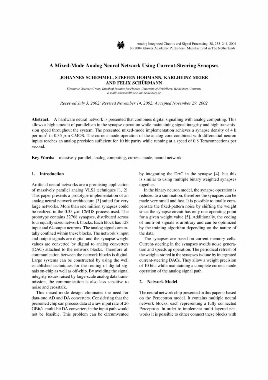
Fig. 1. Left: recurrent network, right: configured as a two-layernetwork by setting some synapses to zero (dashed lines).
each other or to configure a block as a recurrent net-work. As illustrated in Fig. 1, multi-layered networkscan be emulated by feeding back some of the outputsand setting the appropriate weights to zero. The net-work needs a finite time �t to propagate a signal froman input to its outputs. Therefore it can implement acertain range of time delays by using recursion, mak-ing it possible to generate or analyze spatio-temporalinformation.
Since the individual neurons use digital inputs (I j )and outputs (Oi ), the weight multiplication is reducedto an addition and the activation function g(x) equalsthe Heaviside function �(x):
Oi = g
( ∑j
ωi j I j
), g(x) = �(x), I, O ∈ {0, 1}
(1)
To calculate the output of a network block a in asystem built from multiple, recurrent network blocks,the following equation can be used:
O(t + �t)ai = �
( ∑j
ωi j I (t)aj +
∑k
ω′ik O(t)a
k
+∑
l
ω′′il O(t − n�t)b
l . . .
)(2)
�t denotes the time needed for one network cycle. Thefirst term in the argument of the activation function isthe external input to the network block (I a
j ). The sec-ond term models the feedback path from the output ofblock a (Oa
k ) back to its input. The last term showsan exemplary connection from a second network blockb (Ob
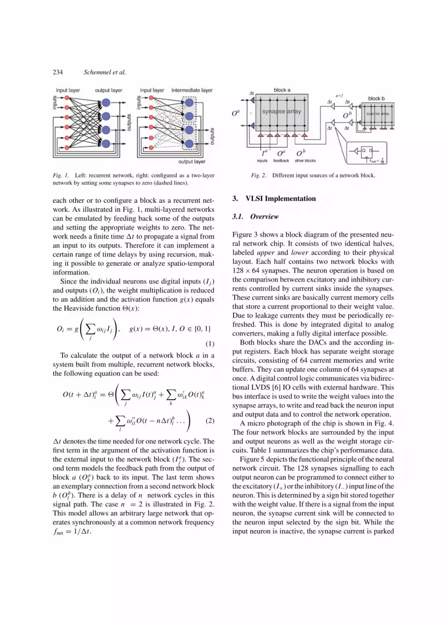
l ). There is a delay of n network cycles in thissignal path. The case n = 2 is illustrated in Fig. 2.This model allows an arbitrary large network that op-erates synchronously at a common network frequencyfnet = 1/�t .
Fig. 2. Different input sources of a network block.
3. VLSI Implementation
3.1. Overview
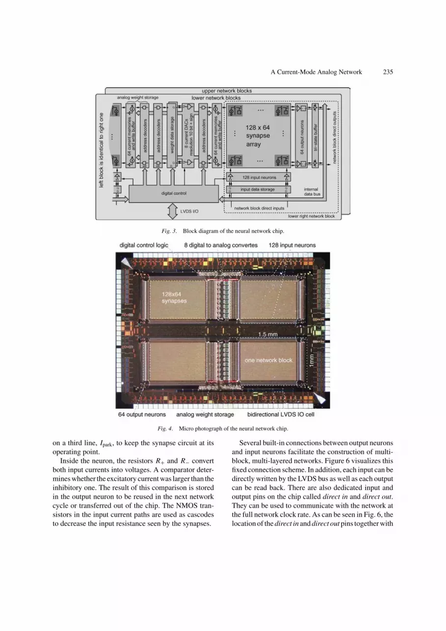
Figure 3 shows a block diagram of the presented neu-ral network chip. It consists of two identical halves,labeled upper and lower according to their physicallayout. Each half contains two network blocks with128 × 64 synapses. The neuron operation is based onthe comparison between excitatory and inhibitory cur-rents controlled by current sinks inside the synapses.These current sinks are basically current memory cellsthat store a current proportional to their weight value.Due to leakage currents they must be periodically re-freshed. This is done by integrated digital to analogconverters, making a fully digital interface possible.
Both blocks share the DACs and the according in-put registers. Each block has separate weight storagecircuits, consisting of 64 current memories and writebuffers. They can update one column of 64 synapses atonce. A digital control logic communicates via bidirec-tional LVDS [6] IO cells with external hardware. Thisbus interface is used to write the weight values into thesynapse arrays, to write and read back the neuron inputand output data and to control the network operation.
A micro photograph of the chip is shown in Fig. 4.The four network blocks are surrounded by the inputand output neurons as well as the weight storage cir-cuits. Table 1 summarizes the chip’s performance data.
Figure 5 depicts the functional principle of the neuralnetwork circuit. The 128 synapses signalling to eachoutput neuron can be programmed to connect either tothe excitatory (I+) or the inhibitory (I−) input line of theneuron. This is determined by a sign bit stored togetherwith the weight value. If there is a signal from the inputneuron, the synapse current sink will be connected tothe neuron input selected by the sign bit. While theinput neuron is inactive, the synapse current is parked
A Current-Mode Analog Network 235
Fig. 3. Block diagram of the neural network chip.
Fig. 4. Micro photograph of the neural network chip.
on a third line, Ipark, to keep the synapse circuit at itsoperating point.
Inside the neuron, the resistors R+ and R− convertboth input currents into voltages. A comparator deter-mines whether the excitatory current was larger than theinhibitory one. The result of this comparison is storedin the output neuron to be reused in the next networkcycle or transferred out of the chip. The NMOS tran-sistors in the input current paths are used as cascodesto decrease the input resistance seen by the synapses.
Several built-in connections between output neuronsand input neurons facilitate the construction of multi-block, multi-layered networks. Figure 6 visualizes thisfixed connection scheme. In addition, each input can bedirectly written by the LVDS bus as well as each outputcan be read back. There are also dedicated input andoutput pins on the chip called direct in and direct out.They can be used to communicate with the network atthe full network clock rate. As can be seen in Fig. 6, thelocation of the direct in and direct out pins together with

236 Schemmel et al.
Table 1. Chip performance summary.
Process features 0.35 µm, 1 poly, 3 metal
Die/core size 4.1 × 3 mm2/3.6 × 2.5 mm2
Synapse size 8.7 × 12 µm2
Blocks/output neurons/synapses 4/256/32768
Supply voltage 3.3 V
Network frequency fnet 50 MHz typ.
Connections/s 1.64 Teracps max.
Weight update rate 400 Megaweights/s max.
Weight resolution 10 bit (nominal) + sign
LVDS bus data transfer rate 11.4 Gigabit/s max.
Fig. 5. Operation principle of the analog neural network.
a routing structure feeding data predominantly from leftto right implies some kind of two layered structure, withthe left half doing preprocessing of the input data andthe right half generating the output signals. The directin signals are connected to the input neurons twice: in-verted and non-inverted. Thereby binary coded signals
Fig. 6. Data flow between the four network blocks.
could be fed into the network in a way that for eachcode value an equal number of synapses is activated.
3.2. Neuron
Figure 7 shows the circuit diagram of the neuron. Itis a multi-stage comparator [7] with current inputs. Itsdynamic input range is about 76 dB: 50 nA resolutionup to a maximum current of 300 µA. The propagationdelay from the current input to the fire output is 15 ns.
The input stage consists of three identical branchesfor I+, I− and Ipark. M2 and M3 act as resistors (R+ andR− in Fig. 5) to convert the input current sunk by theactivated synapses into a voltage. Using the maximumVGS of 3.3 V ensures their operation in the ohmic re-gion for the whole input current range. M4 to M6 formcascodes to provide low input impedance for the threeinputs. The Ipark branch is included into the neuron cir-cuit to match the input characteristics of I+ and I− asclose as possible. M7 to M9 provide a quiescent cur-rent of a few µA to keep the inputs in their operationalregion if no synapse is activated, i.e., the current at aninput is zero.
The voltage comparator that follows the current tovoltage converter is a three stage design to provide thenecessary speed and sensitivity. The first stage is a dif-ferential amplifier with a current mirror load built fromM10 to M14. It provides a high voltage gain over thewhole common mode range. To keep the offset low,M12 and M13 are rather large. This does not comewith a speed penalty since the output resistance of thecurrent to voltage converter is low.

A Current-Mode Analog Network 237
5/.5
1/.6
latch based third stage
2/.4
second stage
10/.5
40/.3
8/2
first stagecurrent/voltage converter
output latch & driver
2/.4M34
M33 M31
M32
Vcas
eval
eval
M30
M29
M18 M24
M28M27
M26M25
M23
M22M21
M20M19
M17
M16
M15
M14
M13M12
M11M10M1 M2 M3
V M9M8bias
Ipark -I+
M7
M6M4
I
I2I1
M5
M36
M37
I4
clearread
fire
I3
M35
Fig. 7. Circuit diagram of the neuron.
The purpose of M16 is to speed up the operation ofthe first stage. If the input changes from a large posi-tive to a small negative voltage difference, or vice versa,the strong output signal generated by the large signalmust be cleared by the considerably smaller responseto the small input signal. Together with the high out-put resistance of the first stage this would lead to anunacceptable delay. Therefore M16 clears any outputsignal prior to starting the comparison at the beginningof each network cycle. M15 acts as capacitor to emu-late the gate capacitance of M10 and M11, thereforeequalizing the capacitances of both output lines. Thisensures that the charge injection caused by M16 doesnot introduce a new offset.
The second stage is formed by two push-pull stages,utilizing M17 to M22 and M23 to M28. They providethe differential input to a dynamic latch which is usedas third stage (M29 to M35). The latch is erased by theclear signal as well (M35). It is activated by the eval andeval lines about 10 nanoseconds after clear has beenreleased. At this time the input signal on the gates ofM31 to M34 is well above 150 mV and therefore muchlarger than the worst case input offset of the latch. Afteractivation the latch amplifies the input to the full powersupply range.
The network cycle is controlled by the read signal,which transfers the neuron state into the output latch
formed by I1 and I2. As shown in Fig. 3, the fire signalcan be either read out from the chip or fed back as aninput signal into a network block.
3.3. Synapse
The circuit diagram of the synapse is depicted in Fig. 8.The main parts are the current sink (transistors M1 toM6) and the sign storage (M7 to M12). Transistors M1
M12M11
M10M9
M7 M8
M6park
evaluate
I
M5
M3M2
M1
I+ I−
writeM4
Fig. 8. Circuit diagram of the synapse.
238 Schemmel et al.
to M4 form the current memory cell. M1 acts as a cur-rent sink, controlled by the voltage on M3, which is con-nected as a capacitor. Since its capacitance decreases ifits gate voltage falls below its threshold voltage VT , thesource voltage of M1 is raised by the voltage drop overthe diode-connected NMOS transistor M2, which hasthe same W/L ratio as M1. M2 keeps the gate voltageof M3 always above VT and also increases the outputresistance of the current sink.
The sign of the synapse is determined by the stateof M9 and M10. While the write signal is active, eitherthe I+ or I− line is set to Vdd by the analog weightstorage unit (see Fig. 3). This causes charge flowing onthe gates of either M9 or M10, letting it conduct andthereby discharge the gate of its crosscoupled counter-part. The charge injection caused by M11 and M12 inthe moment write becomes inactive (switches to Vdd)increases the voltage on the activated side even furtherwhile the other side is held low by the conducting tran-sistor. This ensures that the selected output transistor,either M7 or M8, is switched on. It is also possible todisable a synapse completely by setting both I+ and I−to ground.
During normal network operation the input neuronactivates the synapse with the evaluate signal. This con-nects the current sink to the I+ or I− line, dependingon the state of M9 and M10, i.e., the programmed sign.The current sink is connected to the Ipark line once itis deactivated by the input neuron, thereby keeping thecurrent sink in its correct operational region and avoid-ing voltage drifts at the drain terminal of M1.
The dependency between the gate voltage of M1 andits channel current is not linear and also differs betweeneach synapse due to the transistor parameter variations.Therefore the synapse weight is programmed by a cur-rent instead of a voltage. The current is stored by acti-vating the write signal and keeping the evaluate signallow. Thereby M4 and M6 are conducting while M5isolates the current memory from M7 and M8. M1 willsink any current forced into it through the Ipark inputby the analog storage unit. After deactivating the writesignal the gate voltage necessary to sink the desiredweight current by M1 and M2 is kept on M3. The volt-age error caused by the charge injection of M4 can becompensated by a slight shift in the weight value. Theperiodic weight refresh necessary to compensate theleakage currents will also correct transistor parameterdrifts due to a change in die temperature.
An upper limit for the precision of the synapseweight is given by the kTC-noise of the weight ca-
pacitor M3:
u2c = kT
C(3)
The extracted capacitance of M3 is about 60 fF (thetotal capacitance including all parasitics, M1 and M4is about 20% larger). At a temperature of 300 K thevoltage noise is 0.26 mV. Related to the 1.5 V swingused, this leads to a voltage error of 0.17%. Thereforea precision of 10 bit for the weight DAC is sufficient.
3.3.1. Power Consumption. The total power con-sumption P(N) of a chip with N synapses is:
P(N ) = Pweights(N , ω) + NPsignal + Pstatic (4)
Pweights(N , ω) is the total power dissipation caused bythe weight dependent synapse currents:
Pweights(N , ω) = Vdd Isyn
N∑j=1
|ω j| ω j ∈ [−1, 1] (5)
Due to the current-steering between Ipark and I+ or I−in the synapse this value is independent from the inputsignals of a network block. Isyn is the maximum synapsecurrent. Psignal is the input dependent power needed persynapse while Pstatic sums up the static power consump-tion of the neurons, the weight storage circuits and thecontrol logic and is neglected in the further discussionsince it only adds a constant offset. Psignal is caused bythe input neurons while driving the evaluate signal. Itconnects to every synapse and must be charged when-ever the state of the input neuron changes. Assumingthe worst case, i.e., each input neuron toggles everycycle, Psignal can be calculated (Ceval approximated as10 fF):
Psignal = 1
2
fnet
2CevalV
2dd = 14 µW (6)
The dynamic range of the synapse current is set bythe DAC reference current which is equal to Isyn. Thesynapse is designed for a maximum of 50 µA witha resolution of 50 nA. The weight dependent powerconsumption Pweights exceeds the worst case dynamicpower calculated in Eq. (6) for a weight current of about0.4 µA which is equal to 0.8% of its dynamic range. Im-plementing the synapse as a current storage cell leadsto a total power consumption dominated by signal inde-pendent, i.e. static, currents which are depending pre-dominantly on the weight values. This reduces the noise
A Current-Mode Analog Network 239
and eases power supply. It also allows a control of thetotal current consumption. It might be included in thetraining algorithm to enforce a certain limit.
3.4. Weight Storage
The weight values are written into the network as acombination of a 10 bit magnitude and 2 sign bits. Thesign bits are transferred unaltered into the synapse signlatch (see Section 3.3) while the weights are first con-verted into a current and then stored in a current mem-ory until all 64 weight values needed for one column ofsynapses have been converted. Since a network blockcannot be used for data processing while its weightsare written, a fast weight transfer is desirable. There-fore a two stage structure is employed. Considering thearea needed for a 10 bit DAC with a conversion time ofa few tens of nanoseconds, it was chosen to use eightDACs in parallel for two adjacent network blocks. Ascan be seen on the die photo (see Fig. 4), the DACsoccupy less than 10% of the synapse area. The DACshave a double-buffered input to allow continuous op-eration. Separate current memories and weight buffersfor the left and right network block allow an alternat-ing pattern of filling the current memories at one sidewhile updating the other side’s synapses and vice versa.The input registers of the DACs can be written at thefull interface speed of 3 · 108 16 bit words per second.The conversion time of the DACs is 40 ns. With eightDACs eight conversions are necessary to fill the 64 cur-rent memories of one side. A column of synapses musttherefore be written in 320 ns.
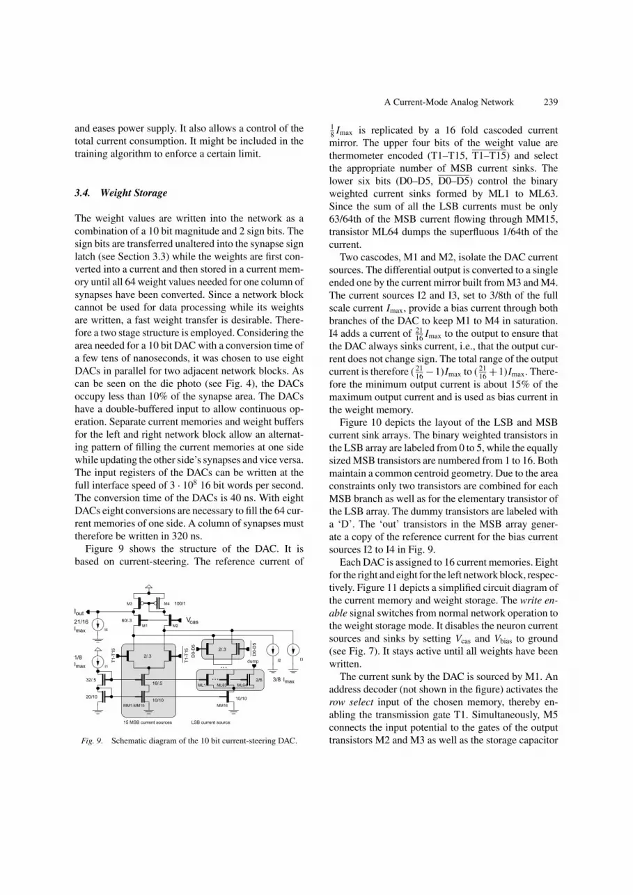
Figure 9 shows the structure of the DAC. It isbased on current-steering. The reference current of
100/1
32/.5
10/10
dump
20/10
16/.5
10/10
casV60/.3
I3
M3
T1-
T15
T1-
T15
M4
M2
LSB current source15 MSB current sources
M1
I1
D0-
D5
ML64
D0-
D5
2/.3
2/.3
ML1 ML63
MM16 MM1-MM15
2/6
I4
I2
maxI
maxI
maxI3/8
1/8
21/16
outI
......
Fig. 9. Schematic diagram of the 10 bit current-steering DAC.
18 Imax is replicated by a 16 fold cascoded currentmirror. The upper four bits of the weight value arethermometer encoded (T1–T15, T1–T15) and selectthe appropriate number of MSB current sinks. Thelower six bits (D0–D5, D0–D5) control the binaryweighted current sinks formed by ML1 to ML63.Since the sum of all the LSB currents must be only63/64th of the MSB current flowing through MM15,transistor ML64 dumps the superfluous 1/64th of thecurrent.
Two cascodes, M1 and M2, isolate the DAC currentsources. The differential output is converted to a singleended one by the current mirror built from M3 and M4.The current sources I2 and I3, set to 3/8th of the fullscale current Imax, provide a bias current through bothbranches of the DAC to keep M1 to M4 in saturation.I4 adds a current of 21
16 Imax to the output to ensure thatthe DAC always sinks current, i.e., that the output cur-rent does not change sign. The total range of the outputcurrent is therefore ( 21
16 −1)Imax to ( 2116 +1)Imax. There-
fore the minimum output current is about 15% of themaximum output current and is used as bias current inthe weight memory.
Figure 10 depicts the layout of the LSB and MSBcurrent sink arrays. The binary weighted transistors inthe LSB array are labeled from 0 to 5, while the equallysized MSB transistors are numbered from 1 to 16. Bothmaintain a common centroid geometry. Due to the areaconstraints only two transistors are combined for eachMSB branch as well as for the elementary transistor ofthe LSB array. The dummy transistors are labeled witha ‘D’. The ‘out’ transistors in the MSB array gener-ate a copy of the reference current for the bias currentsources I2 to I4 in Fig. 9.
Each DAC is assigned to 16 current memories. Eightfor the right and eight for the left network block, respec-tively. Figure 11 depicts a simplified circuit diagram ofthe current memory and weight storage. The write en-able signal switches from normal network operation tothe weight storage mode. It disables the neuron currentsources and sinks by setting Vcas and Vbias to ground(see Fig. 7). It stays active until all weights have beenwritten.
The current sunk by the DAC is sourced by M1. Anaddress decoder (not shown in the figure) activates therow select input of the chosen memory, thereby en-abling the transmission gate T1. Simultaneously, M5connects the input potential to the gates of the outputtransistors M2 and M3 as well as the storage capacitor

240 Schemmel et al.
Fig. 10. Common centroid layout of the DAC LSB (left) and MSB (right) current sinks.
8/140/1128/1
I1 I2
M5
outputpark
M10
M11
write
synapsereplicaS1
M12
S2
M9
M6
I
L1
M3
T1
M2
N1
I3
M8
M7
enablewrite
M4
S3
M1
boost
weight
rowselect
input
signinputs
I+/ I-ouputs
offset
Q
D
en
Qwrite
inII in
enab
le
write
inI
Fig. 11. Schematic diagram of the weight storage circuit.
M4. M3 is used to generate the programming currentfor the synapses. The current mirror M1/M3 reduces thesynapse current to 1/16th of the DAC current. Since itsoutput current is larger than the desired synapse cur-rent due to the bias current included in the DAC out-put, it is necessary to subtract this bias. This is doneby the synapse replica S1 included in the weight stor-age circuit. Before the first row of synapses is written,weight values of zero are sent through the DAC to ev-ery current memory cell. Therefore the current throughM3 represents the bias current. The write offset signal
enables the storage of this current in the synapse S1.While programming the real synapses in the synapsearray the write offset signal is inactive and S1 subtractsthe stored offset current from the current sourced byM3.
While programming a synapse, the potential on theIpark line is not constant since it reflects the gate po-tential necessary to set the synapse to the desired out-put current (see Fig. 8). The capacitance of the Ipark
line together with the actual synapse current determinethe programming time. To reach the goal of 50 nA

A Current-Mode Analog Network 241
synapse resolution and less than 320 ns per column ofsynapses it was necessary to speed up the program-ming. M2 generates a fivefold larger current than M3.Five replica synapses (S3) act as sinks for this current,thereby keeping the drain potential of M2 at nearly thesame level as it will be at M3 after Ipark has reached itsfinal value. The boost signal connects both drain ter-minals together for approximately the first half of theprogramming cycle (the exact time can be configured).This effectively reduces the ratio of Ipark capacitance tosynapse current by six, making it possible to reach thedesign goals. S2 is the equivalent to S1, i.e., a replicasynapse to store the bias current flowing through M3.Like S3 it consists of five replica synapses connectedin parallel to take the width ratio of M2 to M3 intoaccount.
4. Training Results and Measurements
The network chip is operated by an FPGA that loadsthe weights, controls the network timing and readsand writes the network data. There are two differentways to determine the weight values to solve a givenproblem:
– Using supervised learning in a hardware-in-the-loopconfiguration with an iterative algorithm.
– Calibrating the chip and using an established numer-ical algorithm to precalculate the weights.
For the first method, we use an evolutionary algorithm.The weights belonging to an output neuron are assignedto a chromosome with each gene coding one weight.To evaluate the analog performance of the network, then-bit parity problem is used. This is well establishedas exemplary problem for simulated networks [8] aswell as hardware implementations [9]. The network isconfigured to use two network cycles to process onetest pattern, because a neural network needs at leasttwo network layers to solve the parity problem. Thenumber of outputs fed back to the network is equal ton, i.e., the hidden layer is formed by n neurons. Theinput patterns are presented to the chip in random orderand the results are compared with the target data. Thefitness is the total number of binary correspondencesfor all test patterns. The mutation operator replaceseach gene by a randomly selected new one with a fixedprobability (usually 0.5 to 2%). A selection schemeis used that exchanges the worst of a generation with
copies of the fittest ones and a crossover operator isapplied [10].
The most difficult problem trained was 10-bit parity.After 10,000 generations of 50 individuals each thenetwork recognized 99.7% of the input patterns (1021out of 1024). With 8-bit parity, 100% could be reached.To test the generalization capabilities, 16 patterns wereomitted from the 256 test patterns of the 8-bit parityproblem. After successful training, the network wasable to calculate the parity of the 16 formerly unseenpatterns correctly.
The second approach requires knowledge of the off-sets caused by fixed-pattern noise to correct the calcu-lated weights before loading them into the network. Wedeveloped a calibration method that extracts the staticoffset values of the individual synapses, the neuronsand the DAC bias calibration (see Section 3.4). Sincethe only data that can be retrieved from a neuron blockare the fire outputs of the neurons, all the offsets mustbe deduced from this information.
All measurements are based on the following basicprocedure: two or three synapses are set to weight val-ues that would ideally result in I+ = I−. Since the realchip is subject to device variations, the neuron out-put may be zero or one. To find the exact trip point,the weight of one of the synapses is swept across arange centered around the original weight w and largeenough to include all deviations. This is done in LSB in-crements. For each weight value the network responseis evaluated five times. If the neuron has fired threeor more times, the original weight w minus the actualweight value is taken as the result xi . If a, b are thesynapses held at a fixed weight value and i denotesthe synapse weight being swept, Eq. (7) describes themeasurement:
−w
2− σa − w
2− σb + w + σi + xi = y (7)
The unknowns are the synapse offsets σa, σb and σi
as well as the neuron offset y. To calculate them thefollowing four measurements are needed:
−σa + σi − y = −xai (8.1)
σa − σi − y = −xia (8.2)
−σa − σb + σi − y = −xabi (8.3)
−σa + σb − y = −xab (8.4)
The sub/superscript i of x denotes the synapse be-ing swept. The original weight w always cancels and
242 Schemmel et al.
Table 2. Offset measurement results in LSB. The LSB current atthe synapse was 30 nA (Isyn = 30 µA).
Chip 1 Chip 2
Neuron offset width (temporal mean 74 73of spatial rms of neurons)
Synapse offset width (temporal mean 2.4 2.5spatial rms of synapses)
Synapse noise width (spatial mean 2.2 2.3of synapses temporal rms)
Row offset mean (mean of spatio-temporal 10.7 12.4mean of synapse rows)
Row offset width (rms of spatio-temporal 2.9 2.7mean of synapse rows)
is therefore not written. By solving the set of linearEqs. (8.1) to (8.4) σa, σb, σi and y can be calculated.Measurements (8.1) to (8.4) were done for all valuesof i between 2 and 127. For each synapse i , two refer-ence synapses a and b were randomly chosen.1 Synapsecolumns 1 and 128 were excluded to avoid edge ef-fects. This procedure yields all 126 individual synapseoffsets σi as well as 126 values for the neuron offsety. Their mean value was taken as the resulting offsetof this neuron. The measurement for each neuron wasrepeated 100 times to get the temporal variations aswell.
Table 2 shows the results for single network blocksof two different chips. The initial weight value w was5.4 µA (180 LSB). The mean values of the neuron off-set and the synapse noise are zero. The mean value ofthe synapse offsets is calculated rowwise and labeled‘row offset’ in the table. The individual neuron offsetscould be calibrated by using one synapse column. Ifthe network model used requires a bias synapse, bothfunctions can be combined. In terms of the neuron in-put range of −300 to 300 µA the maximum measuredsigma of 2.2 µA is less than 1%.
The low individual synapse offsets are a result ofthe compensation of the fixed-pattern noise of the cur-rent source by the employed current-memory tech-nique. Only the charge injection variation of tran-sistor M4 in Fig. 8 remains, leading to a maximumsigma of the offset distribution of 75 nA. The tem-poral variations of the synapse are about 70 nA,proving that the current-mode operation of the net-work as well as the DAC and the current memoryare insensitive to the switching noise present in thesystem.
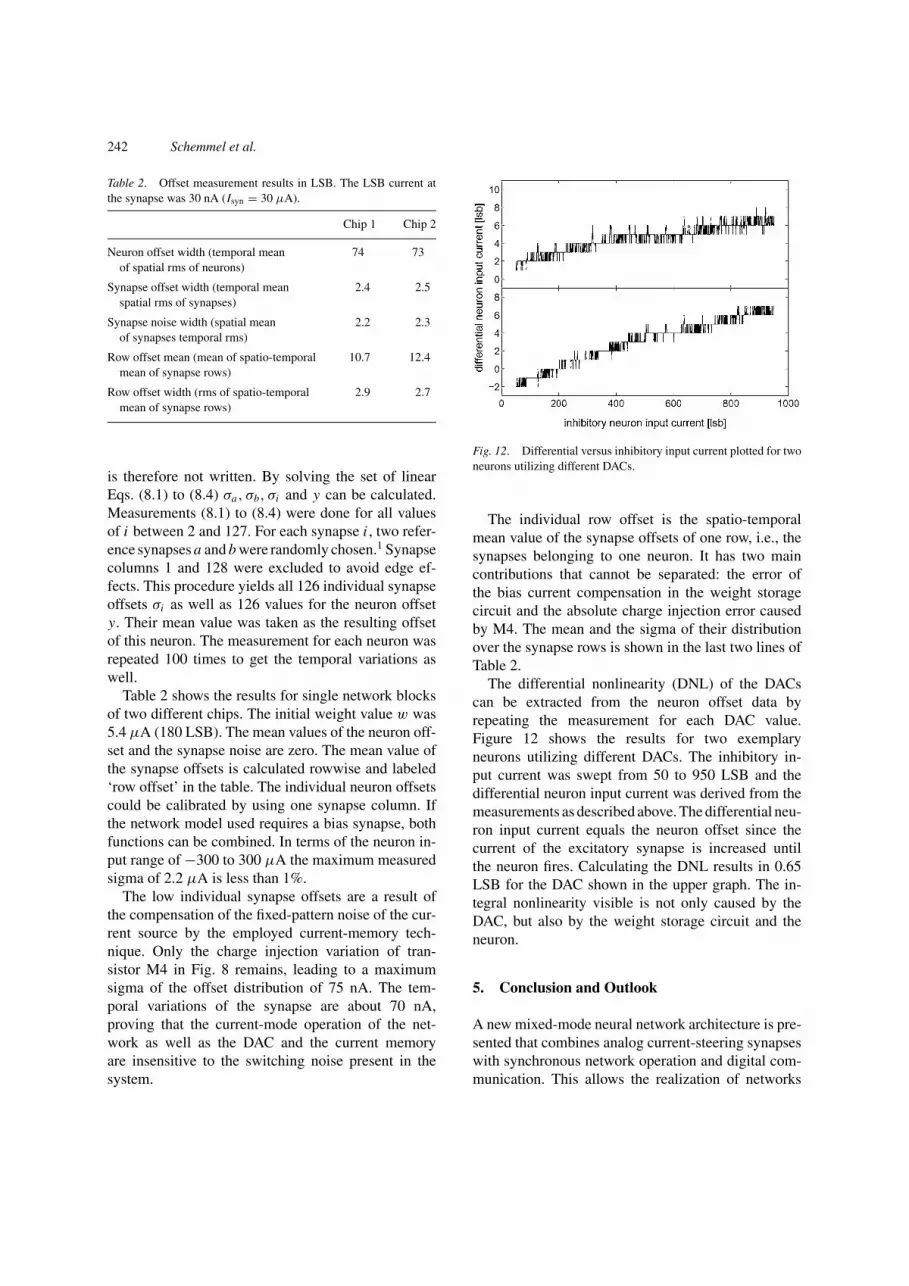
Fig. 12. Differential versus inhibitory input current plotted for twoneurons utilizing different DACs.
The individual row offset is the spatio-temporalmean value of the synapse offsets of one row, i.e., thesynapses belonging to one neuron. It has two maincontributions that cannot be separated: the error ofthe bias current compensation in the weight storagecircuit and the absolute charge injection error causedby M4. The mean and the sigma of their distributionover the synapse rows is shown in the last two lines ofTable 2.
The differential nonlinearity (DNL) of the DACscan be extracted from the neuron offset data byrepeating the measurement for each DAC value.Figure 12 shows the results for two exemplaryneurons utilizing different DACs. The inhibitory in-put current was swept from 50 to 950 LSB and thedifferential neuron input current was derived from themeasurements as described above. The differential neu-ron input current equals the neuron offset since thecurrent of the excitatory synapse is increased untilthe neuron fires. Calculating the DNL results in 0.65LSB for the DAC shown in the upper graph. The in-tegral nonlinearity visible is not only caused by theDAC, but also by the weight storage circuit and theneuron.
5. Conclusion and Outlook
A new mixed-mode neural network architecture is pre-sented that combines analog current-steering synapseswith synchronous network operation and digital com-munication. This allows the realization of networks

A Current-Mode Analog Network 243
with a very high number of synapses by confiningthe analog operation to the individual network blockswhile communication between these blocks is fullydigital. The results from our measurements show thatthe current-mode operation and the differential low-impedance neuron inputs provide a high immunityagainst the noise from the digital parts of the chip. Theusage of LVDS for the external communication allowsthe simultaneous operation of the analog core togetherwith the 11.4 GBit/s link.
After having successfully evaluated the presentedprototype, we plan to realize a chip using the maxi-mum die size available. This would lead to more thanone megasynapse. Since it is possible to skip defectsynapses, neurons or even whole network blocks, yieldis of no concern. As the chip’s power consumption de-pends primarily on the weight values—a synapse con-sumes no power if set to zero—these large networkchips could be densely packed.
An artificial neural network at this scale would allowthe simulation of complex network models founded onneurological evidence.
Note
1. To avoid any crosstalk between selected synapses, the followingconditions were enforced: i , a and b are different and not adjacentto each other.
References
1. S. Satyanarayana, P. Tsividis, and H.P. Graf, “A reconfigurableVLSI neural network.” IEEE Journal of Solid-State Circuits,vol. 27, no. 1, pp. 67–81, 1992.
2. F. Diotalevi, M. Valle, G.M. Bo, and D.D. Caviglia, “A VLSIarchitecture for weight perturbation on chip learning implemen-tation,” in Proceedings IJCNN 2000, IEEE, 2000, vol. 4, pp. 219–224.
3. J. Schemmel, S. Hohmann, F. Schurmann, and K. Meier, “Anintegrated mixed-mode neural network architecture for megasy-napse ANNs,” in Proceedings IJCNN 2002, IEEE, ISBN 0-7803-7278-6, 2002, pp. 2704–2710.
4. B. Boser et al., “An analog neural network processor with pro-grammable topology.” IEEE Journal of Solid-State Circuits,vol. 26, no. 12, pp. 2017–2025, 1991.
5. A. Kramer, “Array-based analog computation.” IEEE Micro,pp. 20–29, Oct. 1996.
6. ANSI/TIA/EIA-644 1995 Telecommunications Industry Asso-ciation, Electrical Characteristics of Low Voltage DifferentialSignaling (LVDS), March 1996.
7. P. Allen and D. Holberg, CMOS Analog Circuit De-sign. Oxford University Press, ISBN 0-19-511644-5, 2002,pp. 483–488.
8. J. Pujol and R. Poli, “Evolving neural networks using a dual rep-resentation with a combined crossover operator,” in Proceedingsof the IEEE International Conference on Evolutionary Compu-tation (ICEC), pp. 416–421, 1998.
9. J. Montalvo, R. Gyurcsik, and J. Paulos, “An analog VLSIneural network with on-chip perturbation learning.” IEEEJournal of Solid-State Circuits, vol. 32, no. 4, pp. 535–543,1997.
10. J. Schemmel, K. Meier, and F. Schurmann, “A VLSI imple-mentation of an analog neural network suited for genetic al-gorithms,” in Proceedings ICES 2001, Springer, ISBN 3-540-42671-X, 2001, pp. 50–61.
Johannes Schemmel received his diploma inphysics and his Ph.D. degree in physics from theUniversity of Heidelberg, Heidelberg, Germany, in1997 and 1999, respectively. Since 1995 he has beenworking in the ASIC laboratory of the KirchhoffInstitute for physics. His research interests includemixed-mode VLSI systems for image processing, im-age sensors, parallel analog computing, analog neu-ral networks and hardware implementations of geneticalgorithms.
Steffen Gunther Hohmann received his diplomain physics from the University of Heidelberg,Heidelberg, Germany, in 2000. Since 2001 he has beenworking as a Ph.D. student in the Electronic Vision(s)group at the Kirchoff Institute for Physics, Heidelberg.His research interests include evolutionary trainingalgorithms and applications for analog neural net-works as well as hardware implementations of geneticalgorithms.

244 Schemmel et al.
Karlheinz Meier is a professor of physics at theUniversity of Heidelberg, Heidelberg, Germany. Heis Vice-Rector of the University. Heidelberg and co-founder of the Heidelberg ASIC laboratory hosted bythe Kirchhoff Institute for physics. He received hisPh.D. degree from Hamburg University in 1984. Hisresearch interests include the application of microelec-tronics in particle physics and medical physics and thedevelopment of sensory substitution systems.
Felix Schurmann received the M.Sc. degree inphysics from SUNY Buffalo, USA, under a Fulbrightgrant in 2000. For his Ph.D. work he then joined theASIC laboratory of the Kirchhoff Institute for Physicsat the University of Heidelberg, Germany. His researchinterest include mixed-mode VLSI systems for ana-log neural networks as well as feasibility aspects ofquantum computing.