a large-signal very low-distortion transconductor for high-frequency continuous-time filters
TRANSCRIPT

946 IEEE JOURNAL OF SOLID-STATE CIRCUITS, VOL. 26, NO. 7, JULY 1991
A Large-Signal Very Low-Distortion Transconductor for High-Frequency
Con tinuous-Time Filters Josk Silva-Martinez, Michel S. J. Steyaert, Associate Member, IEEE,
and Willy M. C. Sansen, Senior Member, IEEE
Abstract-A high-frequency large-signal very low-distortion voltage-to-current transducer is presented. The total harmonic distortion (THD), for supply voltages of only i 2.5 V, is smaller than 0.1% for fully differential input signals up to 2.4 V peak to peak (Vpp). The dynamic range is in the order of 89 dB with the transconductor noise integrated over a bandwidth of 1 MHz. Moreover, this structure presents low sensitivity to transistor mismatches. An operational transconductance amplifier (OTA), based on this transconductor, has been used in an adjustable quality factor 1.8-MNz biquadratic continuous-time filter (CTF). The quality factor Q is controlled, from 2 to 50, with a novel current-source configuration. Both the OTA and the filter have been fabricated in a CMOS 3-pm n-well process. The experi- mental and the expected results are in good agreement.
I. INTRODUCTION URING the last few years, several CMOS fully D integrated high-frequency continuous-time filters
(CTF’s) have been reported in the literature [1]-[5], [lo], 1121. These filters avoid the need of pre- and post-filtering of switched-capacitor filters and offer the possibility of filtering in the megahertz frequency range. Most of these systems use voltage-to-current transducers, operational transconductance amplifiers (OTA’s), and capacitors as the basic components. The main building block in CTF’s, as in active RC and switched-capacitor filters, is the lossless integrator. The integration constant is given by g, /C, where g, is the OTA’s transconductance and C is the associated capacitor.
In CTF’s, unlike to the operational-amplifier-based cir- cuits, the integrators are implemented in open loop. Due to the lack of both virtual grounds and low-impedance nodes, the CTF’s are sensitive to parasitic capacitors and the signal level at the input terminals of the OTA’s is very often large. The former problem and the deviations of the
Manuscript received November 2, 1990; revised March 4, 1991. J. Silva-Martinez was supported by CONACYT, Mexico.
J. Silva-Martinez is with the Elektrotechniek Departement (ESAT- MICAS), Katholieke Universiteit Leuven, B-3030 Heverlee, Belgium, on leave from the Department of Electrical Engineering, Universidad Au- tonoma d e Puebla, Puebla, Mexico.
M. S. J. Steyaert and W. M. C. Sansen are with the Elektrotechniek Departement (ESAT-MICAS), Katholieke Universiteit Leuven, B-3030 Heverlee, Belgium.
IEEE Log Number 9100036.
g, / C ratios due to process parameter tolerances, tem- perature variations, mismatches, aging, etc., have been solved using an on-chip automatic tuning system. How- ever, the nonlinearities of the transconductors, because of the large signal, are a main limitation of the dynamic range in CTF’s. The other limitation is, of course, the noise. In order to increase the dynamic range of the voltage-to-current transducers, several linearization tech- niques have been developed [2], [5]-[91, [111-[131. These linearized topologies previously reported are limited, for low supply voltages, to total harmonic distortions (THD’s) in the order of -50 to -55 dB for voltages smaller than
In addition to the shortcomings mentioned before, nor- mally not severe in low-frequency switched-capacitor fil- ters, there are still other high-frequency effects which are common to all implementations of active filters. Since the active filters are very sensitive to the excess phase of the active blocks, mainly in narrow-band applications, the phase response is of primary importance in the design of high-frequency filters. In narrow-band filters, the time constant associated with the bandwidth (BW) is larger, at least Q times, than this time constant of the resonant frequency. The implementation of this loop with unity- feedback-connected OTA’s is impractical because its fre- quency response degrades for smaller transconductances. The use of partial positive feedback allows the use of transconductances in the same range but the sensitivity to component variations increases further. Another ap- proach uses triode-biased transistors. The frequency re- sponse of these simulated resistors is also limited, mainly for high-resistance values wherein long transistors are needed.
In this paper a large-signal very low-distortion voltage- to-current transducer for high-frequency applications is proposed. Experimental results have demonstrated THD’s lower than -60 dB for fully differential inputs up to 2.4 Vpp in a single-ended OTA prototype. The supply volt- ages are only k2.5 V. Simulated results have shown that for fully differential structures the input voltage range can be increased up to 3 Vpp. Also, the problems associated with the design of high-frequency narrow-band filters are
V P P .
0018-9200/91/0700-0946$01.00 01991 IEEE

SILVA-MARTINEZ E I al.: TRANSCONDUCTOR FOR CONTINUOUS-TIME FILTERS 947
considered, and a technique for the design of filters with both low distortion and high (2 is introduced. The Q is controlled with the output impedance of a current source, avoiding the existence of additional parasitic poles. More- over, most of the distortion introduced by this simulated resistor is even order and can be almost cancelled by current subtraction or voltage subtraction. The paper is organized as follows. The low-distortion transconductor is introduced in Section 11. The second-order effects and the frequency response of the transconductor are dis- cussed in the next section. In Section IV, the design of narrow-band filters is addressed. A second-order filter, based on the proposed transconductor, with Q's ad- justable in the range of 2 to 50 has been designed. Experimental results for both the OTA and the filter are presented in the last section.
11. THE VERY LINEAR TRANSCONDUCTOR
As mentioned in the previous section, some of the most important facts in the design of CTF's are the linearity, the phase response, and the noise of the transconductor. Furthermore, it is very desirable that the linearization technique not be very sensitive to transistor mismatches. An interesting linearization technique was proposed by Nedungadi and Viswanathan [6]. This technique uses two matched nonsymmetrical differential pairs, or a feedback loop [7], in order to generate additional current for ad- justing the bias current of the normal differential pair. Unfortunately, the nonsymmetrical differential pairs in- crease the noise and the additional nodes are a limitation for the frequency response. Furthermore, due to the feedforward compensation, this technique is very sensitive to transistors mismatches [I 11. Techniques using class-AB input stage [SI, and also the ones using bias offset, require higher supply voltages. Moreover, their frequency re- sponse is limited. Techniques using odd and even nonlin- earity cancellation improve the transconductor linearity. THD's lower than -60 dB for input signals up to 2 Vpp and supply voltages of + 5 V have been reported, but the noise increases [9], [IO]. Moreover, because the linearity depends on the gate voltage, for low supply voltages the linearity is reduced. Perhaps the source-degeneration technique is the most natural high-frequency linearization scheme. In fact, this technique has been used in high- frequency applications taking advantage of the drain-source conductance of CMOS transistors biased in the linear region. Furthermore, the zero generated by the source degeneration can be used to compensate the ex- cess phase lag introduced by the OTA parasitic poles [5]. The topology proposed by Krummenacher and Joehl [12] is basically a source degeneration structure for small signal, and an additional internal feedback which in- creases the transconductance for large signals. This last fact increases the linear range of this topology in the order of a factor of 2. Besides, the frequency response of this structure is quite good. This topology is shown in Fig. l(a). Another approach, proposed by Torrance et al. [13],
T
(b)
Fig. 1. Linearized voltage-to-current transducers: (a) Krummenacher and Joehl's topology and (b) Torrance et a/.'s topology (n = 2).
uses a series of differential pairs, such that the input voltage is split in the sections (see Fig. l(b)). Because the input voltage for each section is V d / n , n being the number of sections, the transconductance is also reduced by the same factor n and the third harmonic distortion, the most important, is decreased by a factor n2. Unfortu- nately, the phase response degrades rapidly for more than three sections.
Assuming an ideal quadratic law for the transistors, the single side output current of the source-degenerated structures can be described generally by
with V, the differential input voltage and I , and VGs the transistor bias current and the gate-source bias voltage, respectively. V, and PI are determined by technological and geometrical parameters [14]. For a typical CMOS process the threshold voltage VT is in the order of 0.7 to 1 V. So, for supply voltages of k2.5 V, VGs - V, should be smaller than 0.6 V in order to avoid the reduction of the common-mode range. The factor n is given by I + p, /4P2 for Krummenacher and Joehl's structure. It has to be noted that for this structure this is only valid before the feedback mechanism occurs. For Torrance et al.'s topology n represents the number of sections. Because VGs cannot be increased further, the harmonic distortion can only be reduced by increasing factor n , which implies
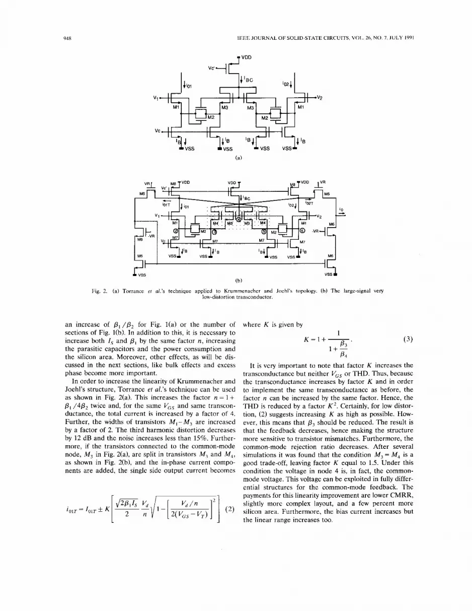
948 IEEE JOURNAL OF SOLID-STATE CIRCUITS, VOL. 26, NO. 7, JULY 1991
Fig. 2. (a)
(b)
low-distortion transconductor. Torrance et al.'s technique applied to Krummenacher and Joehl's topology. (b) The large-signal very
an increase of P I / & for Fig. 1(a) or the number of sections of Fig. l(b). In addition to this, it is necessary to increase both I , and PI by the same factor n, increasing the parasitic capacitors and the power consumption and the silicon area. Moreover, other effects, as will be dis- cussed in the next sections, like bulk effects and excess phase become more important.
In order to increase the linearity of Krummenacher and Joehl's structure, Torrance et al.'s technique can be used as shown in Fig. 2(a). This increases the factor n = 1 + P , /4P2 twice and, for the same V,, and same transcon- ductance, the total current is increased by a factor of 4. Further, the widths of transistors M , - M , are increased by a factor of 2. The third harmonic distortion decreases by 12 dB and the noise increases less than 15%. Further- more, if the transistors connected to the common-mode node, M3 in Fig. 2(a), are split in transistors M , and M4, as shown in Fig. 2(b), and the in-phase current compo- nents are added, the single side output current becomes
where K is given by 1
K=l+--. - P3 ( 3 )
I + - P4
It is very important to note that factor K increases the transconductance but neither VGs or THD. Thus, because the transconductance increases by factor K and in order to implement the same transconductance as before, the factor n can be increased by the same factor. Hence, the THD is reduced by a factor K2. Certainly, for low distor- tion, (2) suggests increasing K as high as possible. How- ever, this means that P3 should be reduced. The result is that the feedback decreases, hence making the structure more sensitive to transistor mismatches. Furthermore, the common-mode rejection ratio decreases. After several simulations it was found that the condition M3 = M4 is a good trade-off, leaving factor K equal to 1.5. Under this condition the voltage in node 4 is, in fact, the common- mode voltage. This voltage can be exploited in fully differ- ential structures for the common-mode feedback. The payments for this linearity improvement are lower CMRR, slightly more complex layout, and a few percent more silicon area. Furthermore, the bias current increases but the linear range increases too.

SILVA-MARTINEZ et al. : TRANSCONDUCTOR FOR CONTINUOUS-TIME FILTERS 949
111. SECOND-ORDER EFFECTS AND FREQUENCY RESPONSE
The derivation of the transconductor output current in the previous section, (21, was based on the ideal quadratic voltage-current relationship. This is, of course, only a first-order approximation. In practice, several second- order effects like bulk effects, mobility degradation, finite output conductance, and transistor mismatches limit the validity of this equation. Some of these second-order effects are discussed in this section.
A. Second-Order Effects
Since the bulk of the n transistors is connected to V,,, due to the large signal the most important second-order effect comes from the body effect. This body effect affects the VT of the transistors and the conductance of the triode-biased transistors M , [14]. In order to take into account these effects, the transistors M , are modeled by
with 77 being the conductance-degradation factor. This factor 77 and V,, are functions of the source-bulk voltage and of the body-effect coefficient y in the form [141
where d is a fitting parameter with value between 0.8 and 0.5. V,,, is the source-bulk bias voltage and V,, is the source-to-bulk voltage including the ac signal. For the next analysis the output conductances of the saturated transistors and the higher order terms are neglected. The output current of the OTA, shown in Fig. 2(b), can be obtained as
i, = AZs + AIVd + A2Vi + A3V2 + . . . . (7)
AZs is the small dc current due to the transistor mis- matches. The coefficients Ai are defined in the Ap- pendix. The coefficient A , corresponds to the OTA transconductance and is given by
1+- 4P2
The term AVT, reduces the transconductance around 10%. This reduction depends on the technology and on the source-bulk bias voltage (see the Appendix for its definition). The second harmonic distortion and the third harmonic distortion are determined by coefficients A , and A , , respectively. The second harmonic distortion is
cancelled, except for mismatches, by the current subtrac- tion. This is not the case for the third harmonic distor- tion. From (7) and the Appendix, HD3 becomes
HD3 2
It should be noted that for large p1/p2 ratios, HD3 still decreases but is less sensitive to this factor due to the effect of both 77 and AVTI. Furthermore, increasing p1 / p 2 reduces the transconductance and, in order to compen- sate for this reduction, it is necessary to increase both bias current and silicon area. This results in smaller output conductance of the transistors and increases the parasitic capacitors. In this paper p1/P2=1O is pro- posed. For the 3-pm n-well process used and for V, =
Vcs, - VT,, HD3, from (91, is in the order of -65 dB. This distortion should be larger for both p-well and scaled-down technologies.
There are other second-order effects such as transistor mismatches and mobility degradation. The transistor mis- matches unbalance the topology. So, the second-order distortion on node 4 increases, which avoids the exact cancellation of the even-order distortions. Simulated re- sults for input voltages of 2.4 v,,, with 2% transistor mismatches have shown HD2 = 0.15% and HD3 = 0.11% (0.096%, without mismatches). The mobility degradation acts in the transistors like additional source degeneration. So, the transconductance decreases but improves the lin- earity [15]. In the voltage-to-current transducer, transis- tors with minimum length of 6 p m are used. It reduces the mobility effects and also reduces the output conduc- tance of the transistors. The other second-order effects have less effect on the harmonic distortion than those discussed above.
B. Frequency Response
In this section the frequency response of the low-distor- tion input stage is considered. In this analysis, the effects of the parasitic poles due to the cascode transistors and due to the differential-to-single-ended converter are not taken into account. For the differential-mode transcon- ductance only the dominant zero and the dominant pole are considered. Furthermore, the gate capacitor and the effect of the transconductance of M , are neglected. If
950 IEEE JOURNAL OF SOLID-STATE CIRCUITS, VOL. 26, NO. 7, JULY 1991
finally, the conductance in the common node V, is as- sumed to be very small, the differential-mode transcon- ductance is given by
S 1 L -
with
(11)
( 12)
3g0( gm + gmh)
c2( gm + gmb + 2gO) + ('3 + cS)(2g0)
( gm + gmb) ( gm + gmb f4gl))
( gm + g m b + 2gl ) ) (c l + c2 + ' 3 + ' S )
WZd
Opd =
where the transconductances are such that gm = gm, =
gm, / 2 = gm4 / 2 . For the bulk transconductance it is con- sidered that g,h = gmhl = gmb3 / 2 = gm, / 2 . g,, is the drain-source conductance of transistors M2. The capaci- tor C, is the gate-source capacitor of MI and C,; almost of the same value as C , is the addition of the gate-source capacitor of M , and M,. C, and C, are the total parasitic capacitors from nodes 2 and 3 to ac grounds, respectively. For typical low distortion designs g, is much smaller than gm. Hence, the frequency of the zero is dominated by the term 3 g , / C,. Besides, the frequency of the pole is higher than that of the zero. Thus, this pole-zero pair introduces excess phase lead in the small-signal transconductance. This is not necessarily true for the OTA, wherein other parasitic poles must be taken into account.
For common-mode signals the transconductance, ap- proximately, becomes
S 1 + -
w 2 c
WpC
(13) gmg2 + gmh( g3 + g4)
Gm, 2 gm+gmh+g2 l + s
with
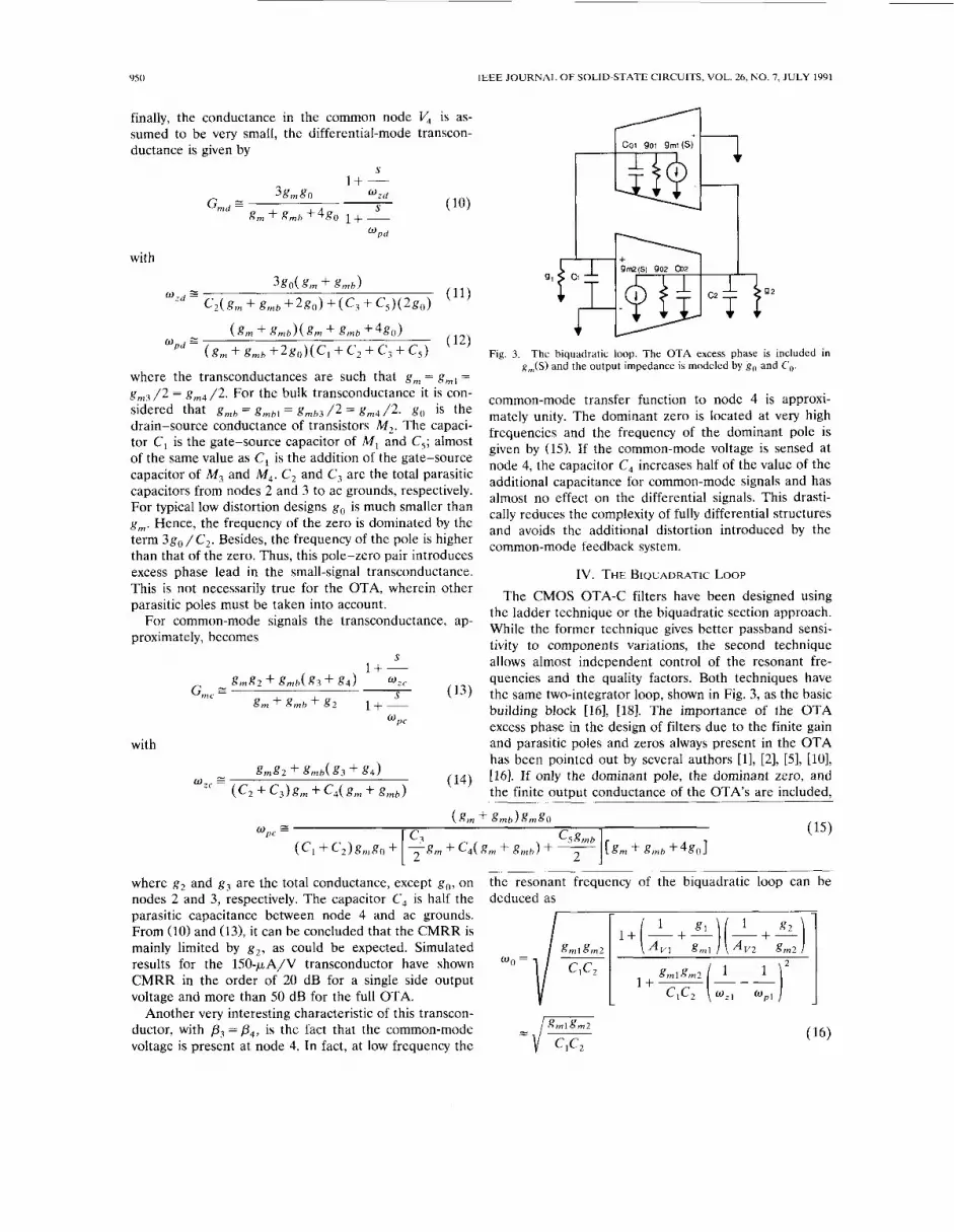
Fig. 3. The biquadratic loop. The OTA excess phase is included in g, (S) and the output impedance is modeled by g,, and Co.
common-mode transfer function to node 4 is approxi- mately unity. The dominant zero is located at very high frequencies and the frequency of the dominant pole is given by (1.5). If the common-mode voltage is sensed at node 4, the capacitor C, increases half of the value of the additional capacitance for common-mode signals and has almost no effect on the differential signals. This drasti- cally reduces the complexity of fully differential structures and avoids the additional distortion introduced by the common-mode feedback system.
IV. THE BIQUADRATIC LOOP
The CMOS OTA-C filters have been designed using the ladder technique or the biquadratic section approach. While the former technique gives better passband sensi- tivity to components variations, the second technique allows almost independent control of the resonant fre- quencies and the quality factors. Both techniques have the same two-integrator loop, shown in Fig. 3, as the basic building block [16], [HI. The importance of the OTA excess phase in the design of filters due to the finite gain and parasitic poles and zeros always present in the OTA has been pointed out by several authors [ll, [2], [SI, [lo], [16]. If only the dominant pole, the dominant zero, and the finite output conductance of the OTA's are included,
where g, and g, are the total conductance, except g,, on nodes 2 and 3, respectively. The capacitor C, is half the parasitic capacitance between node 4 and ac grounds. From (10) and (13), it can be concluded that the CMRR is mainly limited by g,, as could be expected. Simulated results for the lSO-pA/V transconductor have shown CMRR in the order of 20 dB for a single side output voltage and more than SO dB for the full OTA.
Another very interesting characteristic of this transcon- ductor, with p 3 = p,, is the fact that the common-mode voltage is present at node 4. In fact, at low frequency the
the resonant frequency of the biquadratic loop can be deduced as
(16)

SILVA-MARTINEZ rt a/: TRANSCONDUCTOR FOR CONTINUOUS-TIME FlLTERS 95 1
Fig. 4. Second-order filter for high-Q applications. The Q is controlled with the current sources.
where g,ni and A,, = g,, /go; are the transconductance and the dc gain of the ith OTA. w Z 1 and w p , are the frequencies of the dominant zero and dominant pole of OTA1. It is considered that w,, = w z l and w p 2 = wpl. Equation (16) shows that the frequencies of the poles are almost insensitive to both OTA parasitic poles and OTA dc gain. The quality factor can be approximated as follows:
From this equation it can be obtained that even in the absence of parasitic zeros and poles, the maximum Q by this loop is limited by the OTA's finite gain. Combining (16) and (17), the maximum Q is limited to 0.5 A,. This constraint let us conclude the unavoidable use of cascode output stages. On the other hand, the importance of the OTA excess phase is also evident in (17). Even if the frequency of the parasitic poles and zeros is in the order of hundred times w,,, which is quite difficult to achieve for high frequencies, its effect limits the quality factor to values lower than 50, if the frequency of the zero is dominant as is the case in the proposed OTA. The control of the quality factor can be performed adjusting g, and/or g,. For high+ applications it is preferred to control only one of these conductances. Otherwise the controlling conductance should be decreased by a factor of 2. It should be also noted that for high-Q applications the controlling conductance should be very small, typically in the order of several microamperes per volt.
There are several techniques for the implementation of large resistors ( = very small conductances), most of them based on triode-biased transistors [5] . In this approach the resistance is proportional to the length of the transis- tor and hence its frequency response is limited. The techniques applying partial positive feedback [ 171 are very sensitive to variations in the components. The techniques using additional loops for the control of the Q [18] in-
crease the excess phase. The output impedance of current sources has been used in monolithic operational ampli- fiers for many years. This approach avoid the lacks of the previous techniques and allows adjustment of the resis- tance value in a very wide range. The proposed imple- mentation is shown in Fig. 4. The output conductance of the transistors, neglecting the nonlinearities wherein the most important component is HD2, is proportional to the bias current and inversely proportional to the length of the transistor. For a typical CMOS 3-pm n-well process, the Early voltage for NMOS transistors, with length equal to 6 pm, is in the order of 27 V and twice that for the PMOS transistors. The output admittance of the current source is the parallel connection of the output conduc- tance of the N transistor, of the P transistor and the drain capacitors. These capacitors are not very important be- cause they can be absorbed by the automatic tuning system. The current-source output conductance becomes
The advantages of this technique are evident from this equation. The implementation of large resistors, small conductances, requires minimum power consumption and the frequency response is not degraded. Mismatches in the current sources are not critical because the low cur- rent resulting can be easily absorbed by the high current in the output stage of the OTA. The main noise contribu- tion comes from the PMOS transistors, and this can be reduced using small transconductances. Moreover, the linearity is quite good and the most important distortion is HD2.
The filter topology with the input signal connected to a voltage divider, drawn in Fig. 4, was chosen for character- ization. Its dc gain is nearly equal to the dc gain of OTAl. Furthermore, the voltage divider at the input of OTA2 allows the characterization of high Q's without the lack of saturation in OTA1. The biquadratic filter is not exactly a bandpass filter since the conductance go, leaves a finite
952 IEEE JOURNAL OF SOLID-STATE CIRCUITS, VOL. 26, NO. 7, JULY 1991
TABLE I1 OTA SIMULATFD AND EXPERIMENTAL R E ~ U L T S
Simulated ExDerimental Parameter
dc gain 50 dB 45 dB Transconductance 150 p A / V 155 pA/V
Dynamic range 88 dB 89 dB CMRR at 1.5 MHz 52 dB 48 d B PSRR+ at 1.5 MHz 42 d B 40 d B PSRR- at 1.5 MHz 35 dB 30 d B
T H D at 2.4 Vpp -62 dB -60 d B
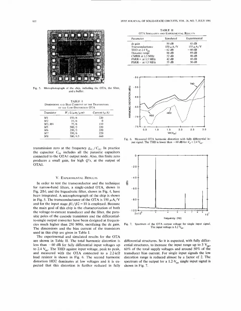
- Fig. 5. Microphotograph of the chip, including the OTA, the filter, g - 5 5 - and a buffer. ?2
TABLE I
OF THE LOW-DISTORTION OTA
Transistor W / L ( p m / p m ) Current ( @ A )
DIMENSIONS A N D BIAS CURRENT OF THF TRANSISTORS
, J
\ ,' I \ t M1 150/6 220 M2 15/6 0 M3, M4 7 5 / 6 110 M5 500/3 330 - 7 5 - I M6 250/3 330 M 7 350/6 220 Vd b'pp)
M 8 500/4.5 660
, , \ I ---,
0.5 1.0 1.5 2.0 2.5 3.0
Fig. 6. Measured OTA harmonic distortion with fully differential in- put signal. The T H D is lower than - 60 d B for Vd < 2.4 VPp
transmission zero at the frequency go , /C( , , . In practice the capacitor C , , includes all the parasitic capacitors
produces a small gain, for high Q's, at the output of OTAl.
connected to the OTAl output node. Also, this finite zero 0
- 2 0
V. EXPERIMENTAL RESULTS - 4 0 Lo
In order to test the transconductor and the technique
Fig. 2(b), and the biquadratic filter, shown in Fig. 4, have been integrated. A microphotograph of the chip is shown
and for the input stage p l / p 2 = 10 is employed. Because
for narrow-band filters, a single-ended OTA, shown in - 6 0
in Fig. 5. The transconductance of the OTA is 150 p A / V
the main goal of this chip is the characterization of both
- 8 0
1 ^ ^
the voltage-to-current transducer and the filter, the para- sitic poles of the cascode transistors and the differential- to-single output converter have been designed at frequen- cies much higher than 250 MHz, sacrificing the dc gain. The dimensions and the bias current of the transistors used in this chip are given in Table I.
The experimental and simulated results for the OTA are shown in Table 11. The total harmonic distortion is less than -60 dB for fully differential input voltages up to 2.4 Vpp. The THD against input voltage, peak to peak, and measured with the OTA connected to a 2.2-kR load resistor is shown in Fig. 6. The second harmonic distortion HD2 dominates at low voltages and it is ex- pected that this distortion is further reduced in fully
3 4 5 6 7 8 9 1 u u
2 X 1 O 6 I o7 frequency (Hz)
Spectrum of the OTA output voltage for single input signal. Fig. 7 . The input voltage is 1.2 Vpp.
differential structures. So it is expected, with fully differ- ential structures, to increase the input range up to 3 Vpp, 60% of the total supply voltages and around 50% of the transducer bias current. For single input signals the low distortion range is reduced almost by a factor of 2. The spectrum of the output for a 1.2-Vpp single input signal is shown in Fig. 7.

SILVA-MARTINEZ et al.: TRANSCONDUCTOR FOR CONTINUOUS-TIME FILTERS 953
I _.__........ - 6
I - s k - - r : L 0.2 0 . 4 0.6 0.8 1 .0 1.2 1 . 4
Vd ( V W )
Fig. 8. Measured harmonic distortions and THD for the filter. The Q factor is 10.
O t t
Y 1 o5 1 o6 1 o7
2 3 4 5 6 7 0 ‘ 2 3 4 5 6 7 8 - 5 0 4
frequency (Hz)
Filter frequency response for different currents in the active Fig. 9. load.
The harmonic distortions of the filter are depicted in Fig. 8. The quality factor for these results is 10. It can be noted that, for voltages larger than 1.2 Vpp, the distortion increases rapidly. This is due to the voltage gain at the output of OTA1. Moreover, this voltage is in phase with the input signal but with a larger swing producing satura- tion in OTA1. The differential signal is in the same order as the input voltage. This distortion is in the same order as the distortion presented by the OTA with single input signals, hence demonstrating that the distortion intro- duced by the current sources is negligible. The frequency response of the filter for different bias currents in the active load is shown in Fig. 9. The bias currents of the current sources are 10, 75, 150, and 250 PA. The peak gain is almost inversely proportional to the filter band- width and almost proportional to the Q factor. The wide Q tuning range of this approach can be clearly noted. The quality factor is limited to be on the order of 50 due to the dominant effect of the zero of the OTA. It is expected
.1 2 3 4 5 6 7 8 1 5 0 4 2 3 4 5 6 7 0 ’
10’ 1 o6 10’
frequency (Hz)
Fig. 10. Filter phase response
for higher frequencies that this Q factor will increase due to the effect of the parasitic poles. The phase response for the same specifications is depicted in Fig. 10. For high frequencies the phase response degrades due to the lim- ited frequency response of the buffer. The effect of the zero due to go , can be clearly noted in both the magni- tude and phase response.
VI. CONCLUSIONS A large-signal very low-distortion voltage-to-current
transducer for high-frequency applications has been intro- duced. It has been experimentally known that in a single- ended OTA the input voltage range can be increased up to 2.4 Vpp while the THD is lower than - 60 dB. However, it is expected that this range can be increased using fully differential structures. The dynamic range is in the order of 89 dB with the noise integrated in a bandwidth of 1 MHz. Also, a technique for narrow-band applications is proposed. This technique uses the output conductance of current sources. It allows control of the quality factor with the bias current of the sources and as result can tune the Q with more than 1 decade, without sacrificing frequency response or linearity. The ac characteristics of both the OTA and the high-Q technique have been experimentally probed in a second-order filter in which quality factors from 2 to 50 have been experimentally obtained.
APPENDIX
In this appendix the coefficients of (7) are given. The effects of the common-mode signals present in the struc- ture are included in these coefficients. The output current of the OTA can be obtained by solving a fundamental fifth-order equation. In order to get certain inside the topology, after several approximations, this equation has been reduced to a set of two second-order equations. From the solution of these equations the coefficients

954 IEEE JOURNAL OF SOLID-STATE CIRCUITS, VOL. 26, NO. 7, JULY 1991
0.75AA2 PI( 7 - AVI-,) 2 ( 1 - 2 A v T l ) + ( A l A v T , ) A =-
4 2 - I4(1+$J
become
A , = 0.75 4- l+ -
(1-AV7-1) PI 4P 2
.
The factors AVT, are determined by the difference of the threshold voltage of transistors M , and M , . These factors are computed as
The definition of factor y can be found elsewhere [141. For the process used y = 0.3
REFERENCES
[1] C. S. Park and R. Schawman, “Design of a 4-MHz analog inte- grated CMOS transconductance-C bandpass filter,” IEEE J. Solid- State Circuits, vol. 23, pp. 987-996, Aug. 1988.
[2] H. Khorramabadi and P. R. Gray, “High frequency CMOS continu- ous-time filters,” IEEE . I . Solid-State Circuits, vol. SC-19, pp. 939-948, Dec. 1984.
[3] M. Banu and Y. Tsividis, “An elliptic continuous-time filter with on-chip automatic tuning,” IEEE J. Solid-State Circuits, vol. SC-20, pp. 1114-1121, Dec. 1985.
[4] Y. Tsividis, M. Banu, and J. Khoury, “Continuous-time MOSFET-C filters in VLSI,” IEEE J. Solid-State Circuits. vol. SC-21, pp. 15-29, Feb. 1986.
[SI Y. T. Wang, F. Lu, and A. A. Abidi, “A 12.5 MHz CMOS continuous time bandpass filter,” in ISSCC Dig. Tech. Papers (New York), Feb. 1989, pp. 198-199.
[61 A. Nedungadi and T. R. Viswanathan, “Design of linear transcon- ductance elements,” IEEE Trans. Circuits Syst.. vol CAS-31, pp. 891-894, Oct. 1984.
[7] E. Seevinck and R. W. Wassenar, “A versatile CMOS linear transconductor/square-law function circuit,” IEEE 1. Solid-State Circuits, vol. SC-22, pp. 366-377, June 1987.
[8] K. Bult and H. Wallinga, “A class of analog CMOS circuits based on the square-law characteristic of an MOS transistor in saturation,” IEEE J. Solid-State Circuits, vol. SC-22, pp. 357-365, June 1987.
[9] Z . Czarnul, S. C. Fang, and Y. Tsividis, “Improving linearity in MOS fully-integrated continuous-time filters,” in IEEE Proc. ISCAS (San Jose, CA), June 1986, pp. 1169-1172.
[lo] V. Gopinathan and Y. P. Tsividis, “A 5V 7th-order elliptic analog filter for digital video applications,” in ISSCC Dig. Tech. Papers (San Francisco, CA), Feb. 1990, pp. 208-209.
[ I I ] P. M. Van Peteghem, B. J. Haby, H. M. Fossati, and G. L. Rice, “ A very linear CMOS transconductance stage for OTA-C filters,” in Proc. IEEE Custom Integrated Circuits Conf. (San Diego, CA), May 1989, pp. 25.3.1-25.3.4.
[12] F. Krummenacher and N. Joehl, “A 4-MHz CMOS continuous-time filter with on-chip automatic tuning,” IEEE J. Solid-Slate Circuits, vol. 23, pp. 750-757, June 1988.
[13] R. R. Torrance, T. R. Viswanathan, and J. V. Hanson, “CMOS voltage to current transducers,” IEEE Trans. Circuits Syst., vol.
[141 Y. P. Tsividis, Operation and Modeling of the MOS Transistor. Singapore: Mc Graw-Hill International Editions, 1988.
[15] S. L. Garverick and C. G. Sodini, “Large-signal linearity of scaled MOS transistors,” IEEE J . Solid-State Circuits, vol. SC-22, pp. 282-286, Apr. 1987.
[16] A. S. Sedra and P. 0. Brackett, Filter Theory and Design: Actice and fassir.e.
[17] R. Tarmy and M. S. Ghausi, “Very high-Q Insensitive active RC networks,” I€€€ Trans. Circuit Theoty, vol. CT-17, pp. 358-366, Aug. 1970.
[181 R. L. Geiger and E. Sanchez-Sinencio, “Active filter design using operational transconductance amplifiers: A tutorial.” IEEE Circuits Derices Mag., vol. I . pp. 20-32, Mar. 1985.
CAS-32, pp. 1097-1104, NOV. 1985.
Champaign, IL: Matrix Publishers, 1978.
Jose Silva-Martinez was born in Tecamachalco, Puebla, MCxico, on August 15, 1955. H e re- ceived the B S degree in electronics from the Universidad Autonoma de Puebla, Mtxico, and the M.S.E. degree from the Instituto Nacional de Astrofisica Optica y Electronica (INAOE) in 1979 and 1981, respectively. Since September 1988 he has been with the Elektrotechniek De- partment (ESAT-MICAS) of the Katholieke Universiteit Leuven, Herverlee, Belgium, where he is working towards the Ph D degree. He has
a fellowship from CONACYT, Mtxico From 1981 to 1983 he was with the Electrical Engineering Depart-
ment of the INAOE, working on switched-capacitor circuit design. H e joined the Department of Electrical Engineering of the Universidad Autonoma de Puebla in 1983 and currently holds the rank of Assistant Professor. His current field of research is in the design and fabrication of integrated circuits for telecommunication applications.
Michel S. J. Steyaert (S’85-A’89) was born in Aalst, Belgium, on April 30, 1959 He received the engineer’s degree in electrical and mechani- cal engineering from the Katholieke Universiteit (K U ) Leuven, Heverlee, Belgium, in 1983 and the Ph D degree in electronics from the Kdtholieke Universiteit Leuven in June 1987
From 1983 to 1986 he obtained an IWNOL fellowship which allowed him to work as a Re- search Assistant in the Laboratory ESAT at K U Leuven In 1987 he was responsible for
several industrial projects in the field of analog micropower circuits at the Laboratory ESAT as an IWONL Project Researcher In 1988 he was a Visiting Awstdnt P r o f e m r dt the University of California, Los Ange- les Since 1989 he has been appointed as a NFWO Research Associate at the Ldboratory ESAT, K U Leuven, where he has been an Associate

SILVA-MARTINEZ et (11 . : TRANSCONDUCTOR FOR CONTINUOUS-TIME FILTERS 955
Professor since 1990. His current research intereFts are in high-frequency analog integrated circuits for telecommunications.
by the N.F.W.O. (Belgian National Foundation) as a Research ASSoCldte at the Laboratory Elektronika, Systemen. Automatisatie, Technologie (ESAT), Katholieke Universiteit Leuven, where he has been full Profes-
Willy M. C. Sansen (S’66-M’72-SM’86) was >or since 1981. Since 1984 he has been the Head of the Department of born in Poperinge, Belgium, on May 16, 1943. Electrical Engineering. In 1978 he spent the winter quarter as a Visiting He received the engineering degree in electron- Assistant Professor at Stanford University, Stanford, CA, in 1981 at the ics from the Katholieke Universiteit Leuven, Technical University Lausanne, and in 1985 at the University of Penn- Heverlee, Belgium, in 1967 and the Ph.D. de- sylvania, Philadelphia. His interests are in device modeling, in design of gree in electronics from the University of Cali- integrated circuits, and in medical electronics and sensors. fornia, Berkeley, in 1972. Dr Sansen IS a member of the Koninklijke Vlaamse Ingenieurs
In 1968 he was employed as an Assistant at Vereniging (K V I V.), the Audio Engineering Society (A.E.S.). the the Katholieke Universiteit Leuven. In 1971 he Biotelemetry Society, and Sigma Xi. In September 1969 he received a was employed as a Teaching Fellow at the Uni- CRB Fellowship from the Belgian American Educational Foundation, in versity of California In 1972 he was appointed 1970 a G T E Fellowship, and in 1978 a NATO Fellowship.