900000_102_04.pdf - navy radio
TRANSCRIPT
ELECTRONIC CIRCUITS NAVWIPS
SECTION 4
POWER SUPPLY CIRCUITS
PART A. ELECTRON-TUBE CIRCUITS
SINGLE-PHASE. HALF-WAVE RECTIFIER.
APPLICATION. - Ine single-ptrase, half-wave rectiser i s used i~ d!
types of electrmic equipmmt ior opplicatims rewring hiqh-voltage dc t o low load cuamt. The rectifier ciicuit can be arranged to Iurnist, nejz:ive 0: positive 5iqh-vo!la!e output !a the load,
CHARACTERISTICS. input to circuit i s oc; ouipui is pdsutirij ii. ,
uses nlgh-vomum Gr gas-fi!le? eiect:3n-!uk &ode zs ,- ,!,I-
nv~tput r q u i ~ e s filtering; d-c ou t~u t ripoie frequency 1s equd to primmy line-voltage fiequmcf.
8 a s poor regulation &aracterisIics. Clrcut provides either pos~tlve- or negltive-polarity
output voltage.
CIRCUIT ANALYSIS. G.n.r~l. The single-phase, half-wove rectiiier i s one
of the simplest types of rectifier circuits. ' h e circuit mn- sists of a rectiiier (dicde) in serles with the alternating source md the load. Since the rectiiier conducts in only 0-r "~ection, electro-.~ flow t2ough ibe ioad cmd throug'n the rectiiier once durir.~ ac t . complete cycle of the impress- - ~,cLi f i e r c~~:;"~L>F, Xc"rs a?>; ?:::!E; !b.? lnteiwi of time the plde is psi l ive with ~res?ec! to !k.e !iiommt (cathode). Thus, the electrons flow through the 1333 i:: pulses, one pulse for each psi t lve haii cycle oi ~e cr~:r=sss mltage.
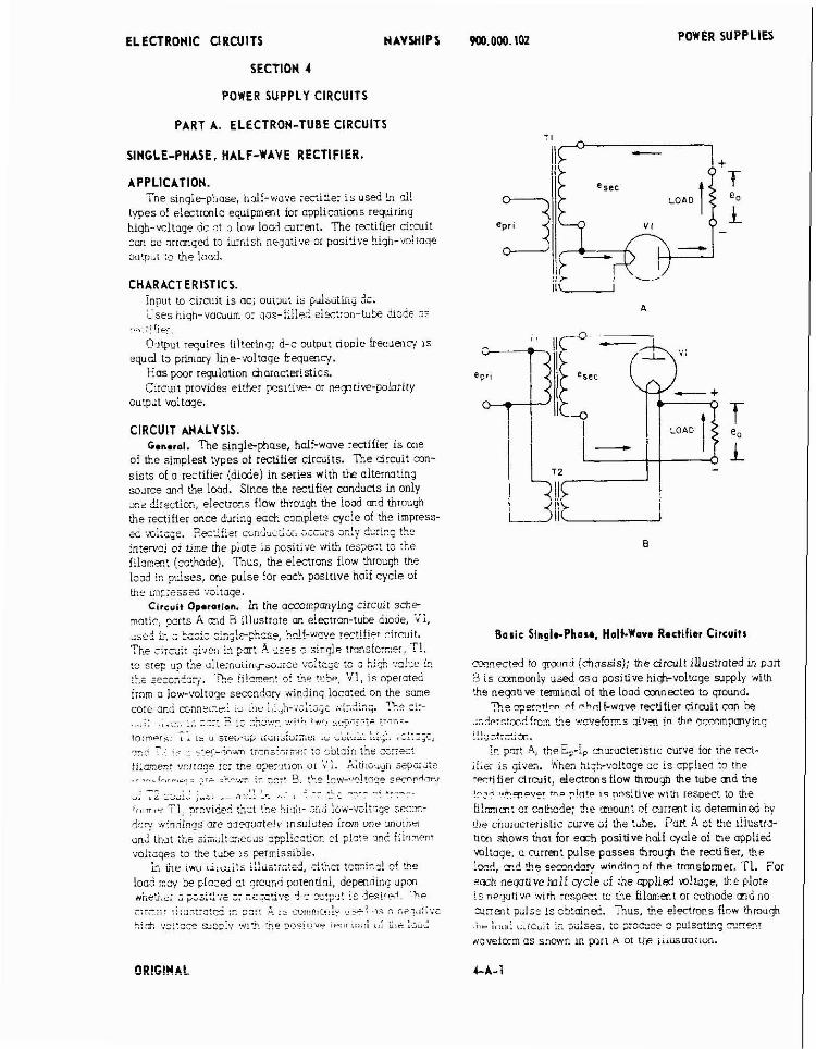
Circuit 0p.roti.n. ln the accompanying circuit sche matic, parts A and 5 illustrate on eiectron-rube d~ode. V i ,
- J :- - L-^i^ -i--l-nhnr.% h"tf-",""~ . ~ ~ , i f i ~ l "il?,,it. " . ' " . . - - ~ . m. i k e n in t A 5 0 s ; sinile f i 3 n ~ f 0 : ~ ~ ~ . TI. :3 sIep UP (he . ~ i i e r n u t i r ~ q s ~ ~ r c e .<ZI:G~E :G z >.i$ .:s!:e L? .L. ...= . ~ : ; ~ - l ~ r ~ . . C , p fi!cm~n! cf , h ~ t s ~ h y V1, i s opersted itom o low-voltage secondary winding locoted on the some core & ccnnrc:& w illc ;,i,:l-;i::zj; ;.i;.?i:.;. T:e 5:-
- , . - - - ---. - . - l--..." -2:. jW,?. .ui-;,;ti ::;;:- .,,., .,,? .... ~ ... . ~. -. , . . . , ,.L !"r*P?s: 1 L 15 c s?ecr"b ~:<,,a~d;z.~. .- ".,.L". .I.,.. .-~.-,..,
n-. - . .: : >IIr>inw~, ir i i j ; i ixe: :0 j:li:i the :C:r?Zt .i<--p7t ..",."". ,nr 7" rr'p el,Jl,o,i 01 ' y ; . x:tjliUl?i, .5epGid;? : : ' .L,~~~ ,~ .....u.,- - .. i -..,-,+i; 7 - i :>,-,*.r i: 2171 5. !LO !3w-.i"!!nIe i..cn"AnN
. . . . ... - > : ~ :.-.L.-".--',."..~.~ ". ._ _""._ ,"i. _. .-7.. ... . . . . . . . .~. ~ ., . -. irirmni I i piovidc6 tk,zt !be i:iai:- :i12 Im-vo!:cji 3 ~ ~ 3 1 -
47% w!ndin" - r e a.lmuatelv insulofw irom one and!"* un2 (hot :he ;i;i.ul:z.cous -p>li;allcr cf ;into 2nd f ~ i l ? ~ ? ? vokzges :a the :-be is permissible . ,
i; Lie LWu Li;wit5 i::ti~trjtd, d:b,c: !71i12! c.! 1ood m y je clcced ot qrouna potenuol, depending upon *he.; . . .- .'"... -. ----. :..* ,:. -. ,.L.ud.- 4-c 32!p:! iz??s3.'ni. :he
c:r,-,::. ::::;?t:?:= : z sc:: 2. i: ,-.;::: <::,::5:y ,?>*? ,;< c, :,e,>:.::.;c . .
"i* ,:-::37e o.L.=~,: ."?I +I. ~ " ' ! l 2 Y C r:i,l:i,~: ..: < . e 1 j i :
POWER SUPPLIES
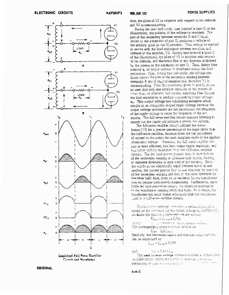
Basic Sln.1.-Phosa. HoICWov. Rectifier Circuits
-nectd tn qmind !dossis): the drcuit illustrated in pan 7. i s mmmonl* used a s o positive bib-voltage supply .with the negutive teminai of the load annected to ground.
3 . e ~ e r 5 t i ~ n ai rrhnlf-wove rectifier d r m i l can be .:-.l.-:r,!mdl:cz the u!o:reb-s $ v a jr! the nrmmpmyinq : , I ,,-..-. : i . . x..
ir p ~ : A, the t,-i, ~ h , ~ a c ! n l s t l c curve ior me r r t - i f i s e n . ?!:,en Ci;!rvcltage zc i s oppi!ed to the rectifier d rmi t , eiectrmsilow Vimugh Vie tube o ld the !n? , : h ~ . e u ~ r me pin!. ,c p n ~ i u v ~ wlul respec1 to me li!,mmt o: =&ode; the mow! of mrrmt i s determined by me c~u iuc~r r i s t i s iuive a: the t h e . PZR A 0: me !liu~:ro- Uon shows tho! ior each positive hali cycle of me applie; mltaqe, a current pulse posses dmu* h e rectifier, the \ -A - A rh* <omnAmy wjndinq nf h e trmsbrmer. T1. For . - -, - . - - . . . . . . . . . . . e ~ h neqauve h i i cycle of L?e qpi ied voltage, the plate i s neqative wlt'h respect to <he iiiammt or cothode m d n o x:n: ~ d : s i s cS!oizd. "us. <?e electrons flnw ihmugh ;>F :,,,d L,;c,,;: ic ~ ~ l s e s , :3 ;redxe 2 ~ d s o t ~ ? ; c7>rr??! "avelorm as snnvn m p i t A 01 t i r i~iusmuor..
ELECTRONIC CIRWITS NAVWIPS
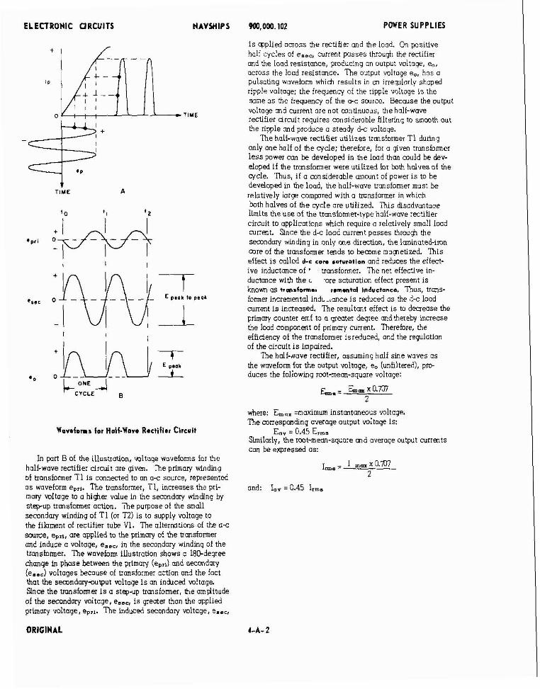
Wovofons tor HoIf-Wove Rectifier Circuit
In port B of the illustration, wltoqe woveforms for the half-wave rectifier arcuit ore aven. ' h e primary winding of transformer T1 is connected to an a s source, represented a s waveform e,,,. The transformer, TI, increases the pri- mary voltage to a higher value in the s a n d m y winding by step-up trmsformer onion. ' h e purposeof the small secondary winding of T I (or T2) is to supply voltage to the filament of rectifier t u k V1. The altercations of the a% mrce, epd, are applied to the primmy of the hmsformer and induce a voltage, e..,, in the secondary winding of the transformer. The waveform illustration shows a 180-degree change in phase between the primary (e,d and secmdory (eSec) voltages because of transformer action and the fact that the secondmyduiput voltage i s an induced voltage Slnce the tmnsformer i s a step-up trmsformer, the amplitude of the secondary voltage, e..., i s greater than the applied primary voltage, ep.i. The induced secondary voltage, e . .~
900.0W.102 POWER SUPPLIES
i s *plied across the rectifier ond the lood. On positive half cycles of esac, current posses through the rectifier md the Load resistance, proc!ucing an output voltage, e,, across the load resistance. The output voltage e,, has a pulsating woveform which results in rn irregularly shaped ripple 'Voltage: the frequency oi the ripple voltage i s the %me a s the freqency of the o-c source. Becouse the output voltage md current ore not mntinuous, the half-wave rectifier a r m i t requires mnsiderable filtering to smmth out the ripple ond produce o steady d-c voltage.
'Ihe half-wave rectifier utilizes trrnsformer T1 during only one half of the q d e ; therefore, for a given transformer less power can be developed in the lmd than a u l d be dev- eloped i f the transformer were utilized for b t h halves of the qc le . Thus, if a mnsiderable m w n t of power i s to be developed in the load, the half-wave transformer must be relatively large compred with a transformer in which both halves of the q d e ore utilized. This disadvmtoqe limits the use of the trmsformer-type half-wave rectifier circuit to applications which require o relatively small lwd current. Since the d c load current passes thrwgh the secondary winding in only me direction, b e inminoted-imn mre of the transformer tends to bemme mametized. Tnis effect i s called d-c core saturation and reduces the effect- ive inductance of ' transformer. The net effeaive in- ductonce with the L ore saturation effect present i s known as t.m~(orm.~ r.mentmi lnduslonce. Thus, trans- former incremental ind~.~ance i s reduced a s the d-c load current i s increased. The resultmt effect i s to denease the primary counter emf to a greater degree andhereby increase the load component of primary current. Therefore, the effidency af the trmsformer isreduced, and the regulation of the circuit i s impaired.
The half-wave rectifier, assuming half sine waves os the waveform for the output voltage, e, (unfiltered), pro duces the following rwt-mean-square voltage:
= Em=xo.707 2
where: Erne, maximum instmtanmus voltage. Tne mrrespmdinq overage output voltage is:
Em, = 0.45 E,,. Similarly, the rmt-rnm-square rnd overage output currents con be expressed as:
ORIGINAL
ELECTRONIC CIRCUITS N A V W I P S WO.wO.102 POWER SUPPLIES
The peek tnv.... voltage of a rectifier tube i s defined as t3e maximum ins tmtnmus voitale in h e direction opposite to that in whi& h e mtifier i s desiged to pass current. "he peak inverse voltage across the rectifier in o half-wwe r ~ t i f i e r drol i t during the period of time that me tube i s nonmndtirtL~g i s app:axima!elj. 2.13 t i m s the .ms M ~ U E of the trmsfomer s e m n 2 q wltcje. %:le peak in- 'verse wltoge con k expressed as:
Eln, = 2.83 Erm where: E,,. = tronsiormer secondary (ai applicdj voltage
' h e output of the rectifier dicuit is mmected to o suit- able filter drali t , t.i smwth th~puisoting direct current for use in the lood circiiit. (Filter circuits 3 : ~ discussed in par! T-, of Section 4.)
F i i i i i R E iHAi;S;S. !ir 9u:pi;t. !z L6e ho!f-wwie rectifier c i i c~~ i t . t h
n w u l p ~ t m n ~ t i ~ c i s !inely lo be iirA1-d tc 3r.e oi hi% pssihle cnusps: c detective rectifier tuoe iopm f~lment j . lhe io& of nppiied o;c witage, or o short& load iiriui; (including shorted fiitersircuit components).
A visd check of a gloss mvelope rectifier rube c n be made to determine whether the iilament is lit; if the filoment is not lit, it nay be ope% or !ne filament rc!ta,;e may not be applied. The !ube filament shou!d be checked ior zontinuity; also, the presence of csrrec! filament vclt- age at the tube socket should be determined by measure ment.
?he a s seaondory voltoge, e..~, shoul? be measured at the tennfnols of transformer T l to determine vhet?er h e wiroqe i s present and 01 a r r r t i i viil~c. Ii'n;i;-ssi;f, meoswe the o ~ p l i d primory wltaqe, e,,b to determine : ! : . 5 r t ! With the :?l.mc?y vcltaze imo;el !;am !;ie ci:ed!!, cwt ino i tv 'resis- tance) measurements of the primow m i semndary ~irniriqs shouid be mode to determine whether m e of h e *in&-,as i s z ~ m , s i x e z zpm !&cm.Lxi>;! i: eiLker winh: wi!!. cause a iock of secondam voiroou. klso, cuntinu;tv meo- surements snodd k made b c t ~ e e n each :iask:iire: :ecCz- dm? termlnol and L!e mrrespondlnq tuoe socket or ioad !ermionl !o dete~mhe whether either one of these ?#o leads i P nnen . - . -. . .
With the pty.ary witage removed iroo Lbe arcui!, re- slstance measurements c m be made ot me outplt tr~~:;mais c! !he r a i f l e r -i,ri~Tt (ocoss load) to determine wheher h e locd d:=it. Lcc!-&fiz th.e fi!ter. is chnjtd; !f the .."D. .. .... -r'.>' ....-.. *--rmm*n= .. .- "n r;wirniui>- miin:isr,; ,:.-.
. . 1esistm.ce meo-,art?%-mPc:- Tade o m s s me ,?siins! ot r2?i r K - k t a ;lr&j: i;Zi .;;:; 'cFzr."'Ej t??. LQe :es!.!-.c ~ : . : . ! . y
c! the ohmmetrr. 'herefore, two measurements must x --in , . ' t i ..~... rnn . rnat . ~ . oi,c ;e,;orcm 1: I re r-:Tr::l! t-1 "L: ,:j
is: ;ne o! the mecsu:emm:s. t2 de!erm~ne (he lmqm ci ( P
w o res1stui;ce meosuienis.k. 7-.E izjii iiji;l:=.;e ;.lilt
is me% nccipted as ine measured voiur. A stloit in Lie m m p a ~ t s J! the filter c:rcu!t or in be load wll cause r c%--z!.:- !cc? n x r ~ ! cc !!nw If ,he rer t i i ler t u b e i s ,: high-vacuuir~ type, the h f f i y load ;Lzer.t r i l l czdsr :tr :!ale !r. become i w t d m i e x 1 3 :Wdlsi? l i o n w Y + a tile c l c e *ss!~s-!: !: -c-ci, z c . ?i -2inw-j li, curitinur.
i- --... A - - " " ^ * - . h -,,, : , " , , , , c . ; , ; , ~ , "'YI 'Sr,"" "C," " .- _. . ..~ ~. . . t a ! i e , 1s use0 11, *,=L.rc&,, " ,,* ..., <=..zi ,.-. =:."b-
will likely result in domoge to the tube, because gas-filled rectifiers me mare susceptible to damage from current over- load thrm are high-vacuum rectifiers.
L o r Output. The rectifier tube should be checked to determine whether the muse oi low output i s low iilommt misson . The l w d a r r e n ~ should be decked to make suie that it i s not excessive, 'woi lse the haltwave rectifier circuit has relutivrly p~fir r+-d~.;on i,< j 1ecccsc :E act- put wltoge c m be cnused by on Increase in lcad current (dsrease in ioad resistonce). Also, the wc secondary wltaqe, e .,,, rmd the primav voltage, e,,,, should be nmsured at terminals of vansiormer T l to d e t m i n e whether mese voltoqes ore present md of the correct value. Short- ed Nms in either the odmaw or secondam windinos will cacse thesecondary voltage to measure below normal. - ---d -m -+ wsi;y <e!ected by res,stm,re mea- -~.u~.-" .-.. ." -- ..-. - suremen!: o ~ l t a g e measuLement i s a more reliable indica- tion. If t'e transformer losses (due to shorted turns) are excessive, the tionsiormer may also k a m e overhmed. inoiler c n e c ~ to derernine wheher h e rians:omer is aeiecuve is to dlsccmnect the secondary ioad (s; ond m a - m e the primaq current with the transformer unloaded; ex- cessive primaq current i s m indication of shorted turns. Sr;!! mother check is to dismnnect d l primor! md secon- dary imds from the transformer terminals ond make mea- surements between the individual windings andthe core, s i n g an ohmmeter or a Megger (insulation tester), to d e !ermine whether any of the windings ore shorted to the care or to the Foraday shield (noise-reduction shield between prirnq and secondmy).
SINGLE-PHASE, FiLL-WAVE RECTIFIER.
APPLICATION. '%e single-phcse, ful!-wave rectifier i s commonly used
in d types of electronic equipnmt for applications re quiring h~rjl-wltoge dc ot o relatively hl$ load current. The rectifier drcuit c.m be orrmqed to furnish neaotive or positive hi$-voltage wtpur to the load
CHARACTERiSf iCS. Lrput to aroli! i s oc; output IS p u i s a ~ g dc. Uses two hi&-vacuum or gas-filled electmn-tube diodes
a s rectitiers, or one twin-dnde rectifier. Output rewires filtering; 6 c wtp l t ripple kequmcy i s
twice the primow line-wltoqe frequmq.
Lt:'<p.At vo.<d,>e
j s e s power iimslormer wirh cmrer-twped, hi@-wiroqe ;.-.:. . . . . .""a *.ria;;.
-. "... ,- . - r ~ ~ - d ~ ~ ANALYSIS. Gsw:;i. 3 s siagie-*,we, i-!!-vave re~tii ier is t i e
most mmmon We oi rectifier circuit used in electronic wuioment. 'The circuit cmsis ts of a hgh-voltage trans- i- ~ r m e r .A.L - ieilier-ta& - .., secondary windmg. a . e plote i i the reccfier tube (sl i s mlect.d to cne end of the - ,,ansfaims s+z~ndz-i, -4 ~ ? e o!h: ate 15 mnnectM to
!he c4ner md. 'Rte iuu" af i f ieGG >?tiax 5 k . z ~ ~ ~ ; , , ~ ~ . .
ii. - -- . L - .._,. i^".i jc: .; ._ _".i ~~ , - , .
ORIGINAL
ELECTRONIC CIRCUITS NAVSHIPS
the secondary winding and the Filament (cathode! of the rectifiers is). Since the secondary n.in?mg is center-top ped, the voltoqe developed in eccn half of !he secondary winding i s in serieswitii theother half; therefore, miy one rectifier p!nte i s ps i t lve or nry iostcn!. As o resuit, electrans !low inioug: r,ne hcif cf the secondmy wwindnq, the load, md o rectifier i i lde on wch hoif cycle of the impressed wltage, with first one diode conducting then the other. n u s , the e!ectrons flow through the load in pulses, one pulse for each haif cycle of the impressed voltaqe.
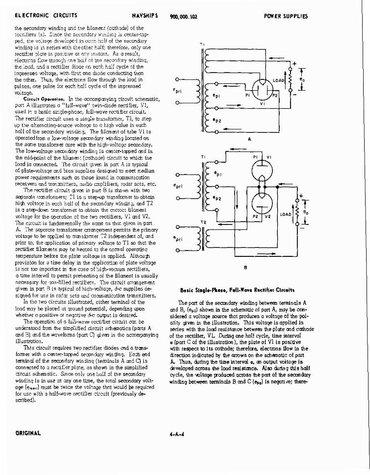
Circuit 0p.rotlon. In the accompanying circuit schematic, port A illustrates a "Full-wove" twin-diode rectifier, V1, used in o h s i c single-phose, Full-wove rectifier circuit. The rectifier circuit uses o single transformer, TI, to step up the olternatinq-source voltage to o high value in eoch holf of the semdory winding. The f i lwent of t u k Vl i s operatedfrom a low-voltage semndary winding located on the same trmsformer mre with the highvoltoge semndory. ?he low-voltage semndory winding i s mte r - tqped md i s the mid-pint of the filament (cathode) circuit lo which the load is mnnected 'The circuit ,$"en in pan A i s typical oi plate-wltoge md bias supplies desir~led to meet medium power requirements such a s those found in communicdion receivers and irmsnitters, oudio amplifiers, rador sets, etc.
?he r ~ t i f i e r drcuit given in pan B i s shown with two w a r a t e rrmsformers: Ti i s o step+p transformer to obtoin hi* voltoqe in eoch half of the semndory winding, md T2 i s a s tpdown transformer tc obtain the mrrect lilarnent voltage for the operation of the twg rectifiers, Vl md V2. ?he circuit i s fundamentally the same os that given in part
?he separate trmsformer arrangement permits the primary voltoqe to be applied tc r rmsbmer T2 independmt of, md prior to, the application of primary voltage to T I so that the rectifier filaments may be heated to the normal operating tmperalure before the plate voltage i s applied. Althou& provision for o time delay in the opplicotim of plate voltage i s not tm L~~portor~t in the case of high-vacuum rectifiers, a time interval to permit preheating of the Bloment i s usually necessary for qas-filled rectifiers. D.e circuit arrmgement given in pm! B i s typical of hiah-voltoqe, bc supplies de- signed for use in radar sets md mmmunicotion transmitters.
In the two circuits illustrated, either terminal of the load may he placed at ground ~ t e n t i d , depending upon whether o positive or negctive & output i s desired.
'The operation of a full-wove rectifier cirojit can be undersmd from the simplified circuit sdematics (parts A m d B) a d the wavebnns (pan C) given in the a c m m p y i n g illustration.
This circuit requires two rectifier diodes ind a trans- former with a center-to~ped semndory winding. Each end t m i n a l of the seamdary windinq (terminals A md C) i s mnnected to a rectifier plate, os shown in the simplified circuit schenotic. Since only m e holf of the secmdary windinq 1s in use at any one time, the total secondory volt- age (e..,! must be twice the voltage that would be required for use with a holf-wave rectifier circuit (previously de- snlbed).
POWER SUPPLIES
The part of the seccndary winding between terminals A and B, (e,~) s h o w in the schematic of part A, may be cim- sidered a voltage source that produces a voltaqe of the pol- arity givm in the illustration. This voltage i s applied in series with the load resistmce betwem the plate m d cathode of the rectifier, V1. During m e half cycle, time interval a (part C of the illustration), the plate of V1 i s positive with respect to i t s mthode; therefore, electrons flow in the direction indicated bf the arrows on the schmatic of p M A. Thus, hrrina the time interval a. m output witace is developed a u o & the load resistm&. A I ~ during &is half wcle. the mltaae ucduced ocmss the DM of the s e a n d a w . . - . winding b e t w m terminals B md C (+,j i s neqztie: there.
ORIGINAL
9OO.OM1.102 POWER SUPPLIES
ORIGINAL
fore, the plate of V i i s negative with respect to its cathode, and V2 i s nonconducting.
During the next &if cycle, time interval b ( p i t C of the illustration), the polarirf of the voltage i s reversed. %.e part of the secondary between terminals 3 m a C ie,zi, shonn in the sAenmtic of go:: 3, pmdcces ,> witole of L?e plarity @"en i? flie il!u;trotion. '>is volt^>? is oppiie: in 4eries with Lhe lood resistmic D?!ween me piuir ui12 cathode of the rectifier, VZ. k i n g .'me internal b (par: C of the illustrotion), the plute of 'JZ is Cas~tIve wit" respect to i t s cothode, md electrcns flow in the direcdon indicated
:he arrows on the shematic of part 3. -?nus, darinq ume interval b, ir, woi:?:! valtngc ir :eveloped ocross the i so l reslst~mie. f h c . ?xin; trls !,oii cycle. the voiragr p r o
z ~ z s s ~i,. pnrt ai the seconCo;y winding between tenninds A and (e,,; :s negacivr K,;, &;r5:c !!i is nanmnductirrg. Tr;:. 5: ,::5.:pf?:rns $"en ln F,:: C . ;t cai; be t iat on!y one recuiier mn?:cts at 25.v ir;:~:: ;.f : i x : 5 , :~ . cr .!t~rmtr -GI: cycies, eiectrnils f l w Lluij,gk. the load resistmice to prodilse 3 :iism;ng 3;:p: ,.vitu:c, s. ?h1s output voltage hos o pulsoung woveiorm whi&
in an ir;cgulc:!y sbiped ripple voltage beemse t?e output voltage andcurrent me not co,ntinucus; the $sq-ency of h e ripple valtuge is rwice the !;ep?mj ~ c ! L4e o-c s u r c p 7 % ~ full-wave rectifier circili! requires filtering to s m ~ t h out the ripple md P ~ ~ U C P 3 s!-oGy d-c volloge.
Tne full-wove rectifier ciriui: ~ u l i z e s tie trans- former (T1) for o g:eoter percentace of the input q c l e lhm the half-wove rectifier, because there o:e tivo pulsations of current in the output !or each coxpiete q d e oi h e applied .~ltemctin. voitoje. ' l h e r e i ~ r ~ , b k $ili-;c:.~. :cr:iier d-- cait i s more efficient, hcs less rutpi)! iippie arnpiibifle.
- ' -..-- ..-'*--- .,,.In,:", 'hT ,he ili~:-w"YF iKfiYei r:,d> >*,~C. ,-.,-,.- .---. , .
,XCCd,C. :,>e 'k !ood cGr:m: y :S5?$ . 31r0 , ;7~, K-, b,?!! D !
of the semndory wlnalng on uiteiniic k.i:: :~.:!ec, :ks?!Ln: In opposite directions in wch La:: of :?e WL?&~::. Simii Sic wkS,3nqs sz e!ezt.icS!v eqml (nmnere urn" to OiF rnother, t+e current passes ikst i r ~ ;,-he :iie;;:z hr x t . i-l!l of me secondor/ winding m: t : ~ iz h e nther llrprtion fnr theother half: thus, here i s r:o tenienzj i:; t ;r trasio.i.er care td bsome pemrmertiy mapetiz&. Furfherrncre, since ';.+I. L- . mle + I , , > ~ o T ~ o ~ ~ .~~ OLC"Ii. Lie e-:j~~t.:e .--Ic:x,:e . n i !he trmsforaer :emaizs re!.t!,ely high. i: 3 ;esdt , the t-axformer 91s mucn hiqher ri!iclc!jiy ihm Lye ::;::;i;;:!!-. -4 +r - kqIh.,7"a rwtifier cir"J!t. --"" -
ELECTRONIC U R C U l i S NAVSHIPS 900.000.102 POWER SUPPLIES
half of the trmsionner secondary. or 1.41 times the m$s wltage across the entire secondary. ?he ?eak inverse wltage can be expressed 0s:
Elnv = 2.83 Em. where: Em, = nus voitoge across half of transformer
semnaary 01, Elnn = 1.41 Em. where: Ems = ms voltage across erfire transformer
secondory The output of the full-wove rectifier circuit i s connected
to a suitable filter circuit to smooth the pulsating direct current for use in the load circuit. (Filter circuits ore dis- cussed in part D of this s ~ t i o n . )
FAILURE ANALYSIS. No Output. In the full-wave r e c t i f i ~ circuit the n o
output mndition i s likely to be Limited to one of three possible causes defective rectifier tube or tubes (open filaments), the l a d of applied o c voltage, or o shorted load circuit (including shorted filter-circuit components).
A visual chwk of qlass-envelope rectifier tube (s) can bemode to determine whether the f i lwmt i s !it: if h e filament i s not lit, the filwent of the tube i s likely to be open or the filament voltage may not be applied. ?he tube filament(s) should be checked for continuity; the presence of correct filament voltage ot the tube socket shouid be de- termined by measurement.
The a-c seoxdar i wltaae a ~ e l i d to each rectifier d a t e - . . should be measured between the secondow center-top i d eorh rectifier plate to determine whether voltooe i s present . . and of the mrrect value. If necessary, measure the applied primary voltage to determine wk,ether it i s present ond of the correct value. With the ~ i m o r y ni tage removed from the cirmit, continuity (resistance) measurements of the primory windng should be mode to determine whether the winding i s opm, since an open (dismntinuity) in the primov windin_: will cause a la& of semndary voltage.
With the primary voltoge removed from tix circuit, r e sistance measurements con be made ot the output terminals of the rectifier circuit (ocrass load) to determine vhether the load ciraiit, including filter, is shorted. If tne filter c i r a i t incorprotes M electrolytic capacitor, the resistance measurements made ocross the output of the rectiiier cir- mi t may vory depending upon the test-lmd polcnt). of the ohmmeter. Therefore, two measurements must k made, with the test leads reversed at the circuit test points fo: one of the measurements, to determine the lar~er of t ie two resistance measurements. The larger resis:mrr value i s then accepted as the measured value. A short in thecom- pnents of the filter circuit or in the lwd will cause an ex- cessive lood current to flow; i f the rectifier-tube type 1s a high-vacuum type, the hmvy iood current will cause the plate to become heated andemit o reddish qlow when the plate dissipation i s exceeded and, if allowed to mntinue, moy result in permanent damage to the tube. If a gas-filled rerufier i s used in thecircuit, excessive lood currmt will likely result in dwaqe to the tube because q~ls-filled rectifiers are more susceptible to damage ' .ram current over- load than are hiqh-vacuum rectifiers.
Low OUWUI. Tne rectifier iub~!sj should be checked to determine whether h e a u s e o f low output i s low filwent miss im. h';o, sicce t i e full-riaue tihe her circuit namally supplies airrent to t+e load m eocn half cfzle, failure of either rectifier or an opol in eiLie: ~ n l f of t$e secondary windinq wiil ollow h e circuit to act a s a holf-wove rectifier circuit, and the output voltage will 5e reduced accordingly. Furthermore. whmeve~ ulis occurs, the ripple amplitude will also increase. md the ripple irewmcy will be thot of the o-c source (instead of twice the source trecplolq). In t i e case of two separate rectifier tubes, if one tube i s lit and the other is not, the trouble i s oSviousl,i assacined with the tube thot i s not lit.
Wit5 t+e primary voltnqe removed fro-., the cirmit, r e sistance measurements can bemade to d e c k the continuity betwem the center-tap md each rectifier plate; this will determine whether one of the windings or plate leads i s open. As an alternative, the a-c s e c m d q voltoge applied to eazh rectifier plote can be measured between the secon- day center-lap and wch rectifier plote to determine whether both wltages are present and are of the conen value.
R e primoy ,voltage should be n s s u r e d to determine whether it i s of the correct ~ialue, since a l a c applied pri- mgry voltage mn result in o low semndary voltage. Also, shorted turns in either the primary or secondary windings will muse tke swandoty voltaje to mwsuie below normal. Shorted turns are not easily detected by resistance mmsurr ment; o voltage aeasurement i s a more relioble indication. If the transformer lcsses (due to short& urns) ore excessive, the trmsformer .nay also become nverheoted. Another d e d r to determine whether the tronsformer i s defective i s to ds connect the secondary loodis) and measure the primary current w~th the tmnsformer unloaded; excessive p r imq current i s an indication of shorted turns. Still another check i s to dismnec: oll primov and secondary leads from h e transformer and make measurements betwem the individud windings and the core, usin: cn ohmmeter or o Meqqer (in- sulation tester), to detemmne whether any of the windings are shorted to tjie m:e or to the Faraday shield (noise reduction shieid between primcry and secondary).
3 e rectiiier-nutput arrent ( to the filter circuit and to fa the Imd) should be checked to mzke sure that it i s within lolerance md i s not excessive. A lowilutput condition due to 3 decrease in lood resistance would cause an increase in lood current; for example, excessive leakage in the cop- acitors of the filter circuit would resdlt in increased lood cur- rent.
SINGLE-PHASE, FULL-WAVE BRIDGE RECTIFIER.
APPLICATION. ?he singlrphase, full-wove >ridge rec;ifier i s used i n
electronic equipmpnt for applications Iequirinq hi&-voltage dc at a hi* load currmL The rectifier circuit can be manyed to furnish neqative o: positive hi&-voltoje output to the load, alLiou& the d io l i t i s ammmly used as a positive hi$-voltoge po.ie~ su;a1:, in xost opplicotions.
ELECTRONIC CIRCUITS
CHARACTERISTICS.
Input to c i r a i t i s ac; output i s pulsating dc. Uses four hi&-vacuum or gasfilled elechon-tube diodes
as rectifiers, or two diodes md one twirrdiode as rectifiers. Output requires !i!teri?.j; &c iiutput ttppie i r e q u o q i s
twice h e primory iir1rvoi:oge frequency. Hos qocd reqdlat~ar. ecracrerisrlcs. Circuit provides either positive- or nemtivepoiarlty
wtpu! voltage. Reqiires three sepcrote filament uansiormers or sepmote
f i lmmt windings for rectifier tiltes. Uses power :ransformet wih sincie hi$-voltoge second-
q windinq; modified cirmit to supply two output volto-jes sirnultmeouslv uses transformer h i 6 imte:-tzpped. blW- voitage secondary winlir~g.
CIRCUIT ANALYSIS.
G.ne.ol. The singlephase, iu:l-wove ~ m a g e rectliler c i ra i t uses two half-wove rectifier tubes m series on eoi5 side of o s i ~ g l e umsformer +I$-valtoge secondor/ winding (me trmsformer secmdav winding does not require o center top); a total of four reclifie:~ sre used in the bridge cirait . &ring mch half q c l e of the impressed o-c wltage, two recufiers, one at mch end of the semndmy, conduct in series to produce m electron flow through the Iond. Thus, electrons flow through the load in pulses, one pulse for each hdf cycle of the impressed voltage. Since two &c output p u l s s ore therefore produced for each complete in- put cycie, full-wave rectilication 1s shined md 6;; ;<:- put i s similar to that of the mnventiond NU-wave rectifier 4.-..<* L.Lb"...
lSne advantage of the bridle rectifier clrcuit aver a coo- vmuonal iuil-wove rectifier is h a t far a $,den :rmsfoxar totd-semndar/ voitage the 5ii;qe i i r - i ! p:o&ces m out- 32: vo!:a:c ,#!.:+ i s nc r ly !w!ce f h q t of the full-wave cir- cult. Another advantage i s that tile p d inverse .ml:oge across m individid iti:i!ie: :25c. ?u::x; tke period of time the hlbe i s nonconductinq, i s opproximotely naif the peak in- verse wltnge across a lute i n o cmventionol iull-wove r e tifia c i m i t der!gal i n produce the sme outpit voltage.
POWER SUPPLIES
One disodvmtooe of the bridle rectifier circuit, however. i s tho1 at least three filament transformers (or three separote windings) are required ior the rectifier tuws.
In many power-supply opplicotims, it i s desiroSle to provide two voltaoes simultaneously - one wltaqe for hi&- >, >; -,cs ,-, .:. --k. . . ,- . . .- . . .r. . ;-. . . . . . lmA..,*e! . . c,,;p;
i'o: k e r e ~ ~ D ~ ! C C ~ : C C S the slnale-xcse. t i i - n ~ t z . 7 ~ . . . . ;x:i62: ci:c;it c z be ~ 2 4 f i P i to +unnlv m odditiond out- put voitoge wiUch i s equal to une half of the voltage pro- vided by the fuL1-wave bridge rectifier circuit.
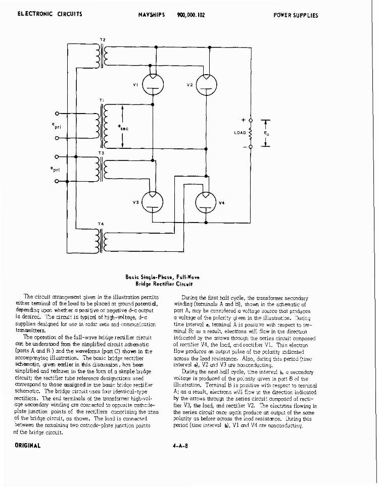
Cirsuit Op.ratiem. A singlephase, full-wove br~dge redtifier i s shown in the ocmrnpmyinq a r a i t sdematic. Four identiml-type electmn-tube diodes, V l , V2, V3, md V4, are mmened in a bridqe circuit a m s s the seandory windinq of transformer TI. E o h tube forms one m oi !he bridge n r m t : the iood is c ln : i r r i d bcine% k; jzck22
points of the bdrmced m s of the bridge. Transformer T I i s a step-up trrmsformer to pmvide high wltoqe ior the bridge rectifiers. R e cirmit ~ V R I Shows three separate iilament uonsforrnss, TZ, T3, zjri ,- T4. .:, ;iz;le lilon:ei:i iransbrmer mmy be used. pm,?..'ed h c t i! itccrporotes three separate f i lwmt swondary windinqs thot are well insulated from m& other and from ground (&assis). Note thot the f i l w m t s of V l and V2 me ot the some m i a t i d with re- s p a to each otha, whereas the f i lm& of V3 md V4 are not. The filmnmts of V 3 md 'v'4 m e mnnected lo OD-
ws i t e a d s of the high-voltage s m n d a r j and thereiore operate m the full p t m t i d d i i f amce that eAsts a m s s the semndary of TI; thus, if ihe f i l w m t s of V 3 md V4 were supplied by a single transfomer winding, the mmmon ,=cU~:~-io~ w ! d g!acs z -hart a c e s 5 he hj&-voltone iemndnry winding. I h e filammts oi V 3 m.' 'J4 must, therebre, be insulated from m d a h e r md must dsn be wdl insulated from ground. In either case, whether three sepmne filcmm! transformers or a single filament ums- former with multiple secondmy windings i s csed, the filoment primory voltage i s opplied independent of, md prior to, the primaty voltage to Ti. R l s arrrmgernent permits the rectifier iilaments to be preheated to the normal operating temperature before the high voltage i s applied to the brldge- redt ier a r a i t .
ORIGINAL
ELECTRONIC CIRCUITS NAVWIPS 900.000.102 POWER SUPPLIES
Basic Single-Phdr*, Full-Wove Bridge Rectifier Circuit
The circuit arrangement given in the illustration permits either tenninal of the lood to be placed at ground potentid, depending upon whether o positive or negative d-c output i s desired. ?he circuit i s typicol of hi$,-voltage, d-c supplies designed lor use in rador sets and communication trmsnitters.
' h e operation of the full-wove bridge rectifier circuit can be underslwd fmm the simplified circuit schenotic (parts A and B and the waveforms (pan C) show in the accompanying illustration. The basic bridge rectifier S d ~ w o t i c , glvm emlier in h i s disolssion, has been simplified and rdravm in the the form of a simple bndge circuit; the rectifier tube reference designations used mrrespnd to those assigned in the basic bridge reciiher schematic. ' h e bridge circuit uses four identicol-type rectifiers. Tne end terminals of the transformer hiqh-voi- age secmday winding are connected to opposlte cothode- piate junction points of the rectifiers comprising the arms 01 the bridge circuit, a s shown. The lood i s connected between the remaining two cothod~plate junction points of the bridge circuit.
During the first holf cycle, the transformer secondary windiny (terminals A md B), shown in the schematic of part A, may be considered o voltage source that produces a voltage of the polarity given in the illustrotion. During time interval a, terminal A i s positive w~th respect to ter- mino1 B: as o result, eiectrons will flow in the direction indicated by the arrows thrauyh the series circuit composed of rectifier V4, the load, ondrectif~er V1. This elecwm flow produces n output pulse of the polarity lndicoted across the load resistance. Also, during this period (time interval 0). V2 and V3 me nonmnducting.
k i n g the next half cycle, time intervol b, o semndoy voitage i s produced of the polarity ylven in port B of the illustration. Terminal B is positive with respect to terminal A: as a result, electrons will flow in the directim indicated by the orrows throu* the series circuit composed of recti- fier V3, the load, and rectifier V2. ?he electrons flowing in the series circuit once oyain produce an output of the slme polcrity os before across the load resistmce. &ring this w i n d (tine intervoi b), V1 md V4 are nonconducting.
ORIGINAL
ELECTRONIC URCUlTS NAVWIPS
I!ii!(!is? Fe!!-Yave Bridge R+ciifi.r i i t cs i i a d T*r.iurm-
ORIGINAL
WO.MM.102 POWER SUPPLIES
From the waveforms given in part C, it mn be sem that two rectifiers conduct at any instant of time: thus. on alternate half q c l e s , electrons flow throuyh the load resistance to produce a pulsating output voltage, e.. This output voltoge has a pulsating waveform, which results in an irrequlorly shaped rip!e ~.~oltoqe because the output voltoge and current are not continuous; the frequency of the iipp:i. v;!:a4e i; :-ice h e f r q e . c y s! the .=c snlice. The iuii-wave bridge recuiier circuit rqu i i r s ii:tering to smmL? out the ripple and pzoduce a steody d-c voltage.
The full-*ave bridge rectifier circuit mokes cmtinuous use of the transformer secondow: therefxe, there ore two pulsations of current in the outpit for each complete cycle of the applied a-c voltage. The d s !cod current posses through the entire secondary winding, flowing in one dlree- "CP. for one hd! cycie oi ne oppiled voirqr, w l i i:: ill=
opposite diretion fcr the other half cycle: thus, there i s no tendency for the transformer core to become petmanendy moqetized. Since little d-c mre saturation occurs, the effective lnaucronce oi t i e tiui,s:sinzi, iiii :>e;eic:c :hc efiiciency, i s relotiveiy high.
The full-wove bridge rectifier, assuming o series of half sine woves as the wavelorm for the output voltoye. eo (unfiltered), produces the following root-mem-square voltage:
Em. = Emor x 0.707 where: L,, = mmimum instontrmeous voltage The corresponding average output voltoge is:
Ea, = 0.9 Ems Similarly, the root-mean-square and average oiitput currents --- !.- *..".*""d "*. - < Ap,b-- ""u.
* ",, i,. = in.= x u . 1 ~ 7 and: I=,. = 0.9 I-s
The peak inrarse v o l t ~ p e across an indlv~duoi rectlilei in a lull-wave bridge rectifier circu~t durmq the period oi time the tube i s iionmnducting is approximately 1.41 times the nns mltaae across the semndmv windina. The secon- -~
voltage, ese., i s applied m two rectifier tubes in series: therefore, since less peok inverse voltage (appmn- motely me halo appwis across each tube, the bridge cir- mi t can b? used to obtoln 0 hlgner ourput voiroge bun L ~ L
be obtained from a cnnvent:onal iu!i-wave rectifier c~rcuit using equivalent rectifier tubes. The peak inverse voltage per wb. can be expressed as:
Elnv (per tube) = 1.41 Em. where: ... Em, = rms voltoge across entire seandary
~ .. . . ... . . , ;r,e cd:FGt 2: !;e !:i:-w3Ve Dr!,l,e fezIiji#?? > l ' ! , , , , > , .- ,, +L- ,,,,I c! the conventiono! full-wove ieniiier clrcult. I n r
recbi'e, pi"";:es twice :be 2;:Fi! ,:2k2;e ! "E
same total transiormer secondary voltcge and A:. outTut zdrer,i zs dWS t>Lc :u;:.:,z;e :sL:;!ie: z:;zc * .::::,; topped seccndav. Tne output ui tnr oriage ititi:iei ci:?,.r is ionnezted tc z suitable !:!tcr ciicui! !- smnnth the PUI- sating i r e c t current !or Lse i? t k 153,i zltzui!. (cil!?: circuits are discussed in tne latter part of this section.)
A vmiotion of the full-wove briige rectifier circuit uses o transformer with o center-topped secmiary winding to supply two output voltages simuitmmusly to two seDa:Gte !gods. The clrcu~t is iundomentoiiy ine same as tho[ giveit e-.i '-- .i.- .,.""-" .;- -.- -..,,.,.., ",,. , ,~ , 7 . - , , ; : *-:,px,;:;r
" L L ' C ' , ."' L'''" ... u "-"" ...?-., ..., . .~ ~ -. . . . , . i. -. -.--, - -: .*;.-,.- ." -;:",: .,,,,- :;,- ::! ,.,m %,? , . ~ .-u.-........r...... ~
4-A-9
transformers md oswriated filamerst circuitry. The reference desiynotions previously assigned remain unchanged.
Sinplifi.d Full-Wave Center-Tap ond Full-Wave Bridge Rectifier Circuit
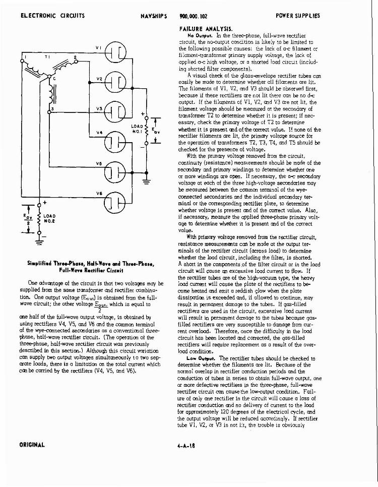
One advantoye of the circuit i s that two voltages m y be supplied from the smne set of rectifiers. One wput voltage (E,.) i s obtained from the output of the bridoe
drolit. the -dartput v o l t a g e h l ~ d i i s q d to 2
one half of the bridge output voltage, i s obtained by using two rectifiers, V3 md V4 of the bridge, and the center top of the seconday winding a s o convmtimd full-wave rectifier circuit. (The operation of the full-wave rectifier circuit was previously described in this section.) Although this circuit wriation can supply w o output voltaqs simul- taneously to two s e p m t e lmds, there is a limitation on the total current which can be carried by the rectifiers, V3 and V4.
FAILURE ANALYSIS. Na Output. In the Full-wave bridge rectifier circuit,
the nwutput condition i s likely to be limited to me of several possible causes: M open filment supply circuit, defective rectifier tubes, the Lack of applied a-c voltaje, or a shorted load circuit (including shorted filter-circuit mmponents) .
A visual check of gloss-envelope rectifier tubes con be mode to determine whether the filaments ore lit. If the filaments are n d a l l lit, the wimary voltoge may not be applied to the filament transformers (T2, T3, and T4). If mly the filaments of Vl and V2 are not Lit, there will be no d-c output from the rectifier circuit, and transformer
ORIGINAL
WO.OW.102 POWER SUPPLIES
T2 .ir b t h tubes 7.q iefzctl,?. The tube ii iments should be check& fcr cortinuity; the presence o! correct fi!an!ent voitage ct the :"be s d e t s ('$1 w d VZ) should be determlned by ~ezsuement . I! necessmy, the primsy md semndav voltages snoul: be checked at tne terminals of trmsformer T2 to determine whether the trmsformer i s defective.
Tne 3-c s e c o n d q voltoge, e,,,, should be measured at the terminals oi trmsiorxer TI to determine whether the voltoge i s present and of mirect vohe. If necessary, measure the applied primory voltage, e,,,, tc determine whetner it i s present 2nd >i tnc -2rrecI ualue. 'Nith the prim%? voitarje rernovec from t ie c~rcut , continuity meosuie- ments of the primary ond secondor, windinus should be made to determine whether one of the windings i s open, since an open (discontinuity) in either windinq will cause a lark of secondary voltoge.
Vith the or;-cv vcl!:;~ re;:oized i:jm the circuit, re- sistance measurements :an be made ot the output teimi- n d s of rhe rectifier circuit ( m o s s laad) to detetmine whether the load circuit, including filter, i s shorted. A short iri the mmponents of the filter circuit or in t h ~ load will cmse an excessive Iood current to flaw. If the recti- fiers are of the hiqh-vacuum type, the heavy load current . . will cause the plates of the rectifiers to become heated and emit a reddish ylow when the plate dissipation i s exceeded and, if allowed to continue, m q result in permanent damage to the tubes. The high-voltorje bridge circuit normally employs yos-filled rectifiers; an excessive load current will very likely result in permanent damaqe to the tubes because they are susceptible to domaqe from current overload. T h e r e fore, once the difficuitv in the load circuit has been located and corrected, the gas-filled rectifiers may require ieplace- ment os a result of the overload condition.
L o r Output. The rectifier tubes should be checked to determine whether the filaments are lit; one or mare defect- ive mti f iers in the bridge con cause the low-output con- dition. Aim, fatlure of only one rectifier in the bridge will allow the circuit to act as o haif-wove rectifier with current supplied to the load on olternote hall cycles only, and the output voltage will be reduced occordinyiy. If rectifier tube Vl or V2 i s not lit, the trouble is obviously associated with the tube that i s not lit: however, if V3 or V4 i s not lit, then L'e trouble moy be either the tube (V3 or V4) or its associated filament timsformer (T3 or T4). The tube f i l m m t should be hecked for continuity; the presence of correct iilcmen: voltsge at the tube socket should Le determined by measurement. If necessmy, the primary ond secondary voltoyes should be checked at the terminals of the filament transfcrmer iT3 or T4) to deter,nine whether the transfcrmer i s detecti.<e.
The locd current should be checked to m&e stlie that it i s not excessive, because a decrease in output voltage con be caused by L? increase in Locd current (dmeose in iood resistance;: for exmple, excessive le&oge in the capacitors of the filter cirmir ..vo,~l+ resuit ir increased load current. Alsc, the n i suc imaiy vc!:a?~, e . . ~ o l d the primary vdtxg?, qDr:, : x ~ ! d >,e v:c?::?f ,! :!?e t e~nIn~!s of trans- former T1 to determine whet'ler these voitoges me of the rcrrect value. Shorted turns in either ii: primmy or secon- Sw ~ h J 3 . g s will cause the ecmiwy ,voltage to measure
ELECTRONIC CIRCUITS NAVWIPS
below normal. Shorted turns ore not easily detected by re- s i s m c e measurement: a voltage measurement i s a more relioble indication. If the transformer losses (due to shorted turns) are excessive, the transformer may also tecome over- heated. .Another check to determine whether the transformer i s defective i s to disconnect the secmdary lmd (5) and mPrsxe the ptimmy cunmt with the transformer unloaded; excessive primary current i s an indication of shorted turns. Still mother check i s to disconnect all primary md secondary leads from the transformer md make measurements between the individual windings and the core, using on ohmmeter or o Megym (insulaticn tester), to determine whether any of the windings ore shorted to the core or to the Fatoduy shield (noise-reduction shield between primary md s m n d q l .
THREE-PHASE. HALF-WAVE (THREE-PHASE STAR) RECTIFIER.
APPLICATION, R e three-phase. half-wave stm or wye-comected
rectifier i s used in electronic equipment for applications where the primary a-c source i s three-phase and the d-c power requirements exceed 1 kilowatt. The rectifier circuit can be arranged to furnish negative or positive hig'n-voltage output to the load.
900,00.M)0.102 POWER SUPPLIES
CHARACTERISTICS. Input to circuit i s threephase ac; output I S dc w~th
amplitude of ripple voltooe less thm that for a sinqle-phose . . rectifier.
Uses three high-vacuum or gas-filled electron-tube diodes os rectifiers.
Output i s relatively easy to filter; d-c output ripple frequency i s y o l to three times we pnmory Line-voitugr frequency.
Has gwd regulation ctiaracteristics. Circuit provides either positjve- or negotivepolarity
output voltoge. Uses multiphase power trmsformer with star- or
wye-connected secondary wm&ngs; primmy windings may be either delta- or we-connected.
CIRCUIT ANALYSIS. G.ner.al. The three-phase, half-wave (three-phase stm)
rpctifier i s the simplest t y p of tNeephose rectifier circuit. The term mre.-phese refers to the primary a-c source, which i s the equivalent of three slngiephase sources, each source supplying o sinewave voltage 120 dqrees out of phase with the others. Fundmentally, this rectifier circuit resembles three single-phase, holf- wave rectifier circuits, each rectifier circuit operating from one phase of a three-phase source and sharing a commm
: :
I TzzT-<H+/ T H R E E - P H I S E SOURCE
0 1 1 1
Szri: Three-Fhosc, i i e i i - * o ~ e j TLr~ - i .Ms . h r )
Rectiticr Circuit
ELECTRONIC URCUITS HAVWIPS
load. The voltaqes induced in the transformer secminry windings differ in phose by 120 deyees; thus, each half- wave rectifier mnducts for 120 deqees of the complete input cycle and contributes one third of the d-c current sup- plied to the load. Electrons flow through tne lwd in pulses, one pulse for each positive hol! cycle of the impressed voltage in each of the three phases; therefore, the outout vdtage has o ripple frequency which i s t!!ree times the frequency of the a-c source.
Circuit Operotion. A h s i c threephase, holf-wave rect- ifier is illustmted in the circuit schematic on wge 4-A-11. The circuit uses a threephase transformer, T1, to step up the alternating source voltage to a high value in t!le star- ar weconnected secondaries. The primxy windlnzs of transformer T i ore shown deli-connected, although in some instances the primary windings moy be wyeconnected (as for a three or four-wire system). The plate of each iec- tifier tube, V1, K2, and V3, i s connected t o o hiyh-voltage secondmy winding. One filament tionsformer, T2, i s ,used to supply the filament voltoge to all three rectifiers since the filaments of the rectifiers me all at the some potential. The primary of trmsformer T2 i s connffted to one phose of the threephase source. The lood i s connected between the junction point of the we-connected secondary windirgs and the filament circuit of the rectifier tubes.
In the circuit illustrated, either terminol of the load muy be ploced ot wound potential, depending upon whether o positive or negative d-c olltput i s desired.
The operation of the three-phase, half-wave rectifier circuit can be understood from the circluit schematic pre- viously given and from the waveforms shown in the occom- Ponying illustration.
Each phase of the three-phase secondmy voltuge i s applied across a rectifier and the mmmon lood ' h e s e conday voltage of phase No.1 (e..,l) i s applied to recti- fier Vl, thesecondory voltage of phase No.2 (e..,2) i s applied to rectifier V2, md the secondary voltage of phose No.3 (e,.,3) i s applied to rectifier V3. The waveform given in the acmmpanying illustrotion as e,,, shows each of the three secondary voltages dispiaced 120 degrees from each other. On positive half cycles of e,.,l. electrons flaw through the-load md rectifier VI; the puke of plate current for rectifier V l i s identified in the illustration as the waveform, V1 i,. On positive half cycles of e,.,2, elecvons flow thmugh the lood md rectifier V2; L!e pulse of plate cu r ra t for V2 i s identified as V2 i,. On positive half cycles of e.,,3. electrons flow throudn the load md rectifier V3; the pulse of plate current for-v3 1s identified as V3i,. F r m the three individual oiotecurrent waveforms i t c m be seen that the s l a t of a conduction period for any rectifier occurs 120 electrical degrees from the stmt of a mnduction period far another rectifier in the circuit. The output voltage, e-, across the load resistonce is determine5 by the instantaneous NIIentS flowing throu* the load; therefore, the output voltage has a pulsating woveform which never drops to zero because of the nature of the rectifier mnduction periods.
If it were not for the overlapping of applied three-phcse secondary voltages, the recti!iers would each conduct for 180 degrees of the cycle; however, during the first 30 d e g e e s of a half cycle, the plate ~f the recufier i s negative
W0.000.102 POWER SUPPLIES
ONE CYCLE PHASE U0.I -i
9p' 1:" 270' 370'
ThrecPham, HalhWore Rectifier Wav.fornr
with respect to i ts positive filment (cathode), and i t mll not mnduct until thepasitive voltage applied to the plate exceeds the d-c output voltage pulsations present onoss the lood md at the fi lment circuit. Also, during the last 30 degrees of a half cycle, the plate i s agoin neqative with respect to the filnment, and rectifier conduction ceoses because the rectifier of mother phose hos stmted to conduct md produce o positive voltaye o a o s s the load. In other wards, each rectifier tube conducts for only we-third cycle, and this results in a series of d-c output voltage pulsations with an irregularly shaped ripple voltoge; the frequency of the ripple voltage i s equal to three times the frequency of the c-c source. Because the ripple frequency i s higher than that of o single-phase rectifier circuit, the three-phase, half-wove rectifier circuit requires less filtering to smooth out the ripple md produce a steady d-c voltage.
In order to keep d-c core saturation to a minimum (because of cunent flowing in one direction only in the secondory windings) and to keep the efficiency relatively high, it is necessary to use a single threephase transform- er in this c i ra i t , rather than three separate singlephase transformers.
ORIGINAL
ELECTRONIC CIRCUITS NAVWIPS W0.000.102
T Z
POWER SUPPLIES
T O O N E P H G E O F T H R E E - P H A S E
S O U R C E
T O T H R E E - P H A S E
S O U R C E
T O T H R E E - P H A S E
S O U R C E
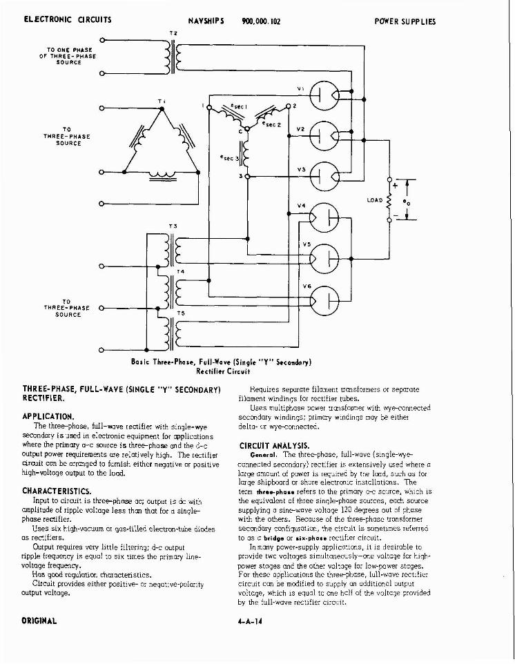
Boric Three-Phase, Full-Wove (Single "Y" Sccondov) Rectifier Circuit
THREE-PHASE, FULL-WAVE (SINGLE "Y" SECONDARY) RECTIFIER.
APPLICATION. The threephase, full-wove rectifier with single-ye
semndory i s used in electronic equipment for cpplicotions where the primary a-c rrurce i s t h r e e - p h a ~ and the d-c Output powm requirements are relatively high. The rectifier drarit can be arranged to furnish either negative or positive
high-voltage output to the load.
CHARACTERISTICS. Input to cirarit i s three-phase ac; output i s dc with
amplitude of ripple vol:age less thcn that for a single- phase rectifier.
Uses six high-vacuum or gas-filled electron-tube diodes a s rectifiers.
Output requires very little filtering; d-c output ripple frequency is equal to SIX times the primov line- voltage frequency.
Has good regulation charnderistics. Circuit provides either positive or negotive-polarity
output voltoqe.
Requires separote filament transformers or separate filament windings for rectiiier tubes.
Uses multiphase power transformer with wje-connected secmdary windings: primary windings may be either delta- or wyrconnected.
CIRCUIT ANALYSIS. tanerol. The threrphose, full-wove (single-we-
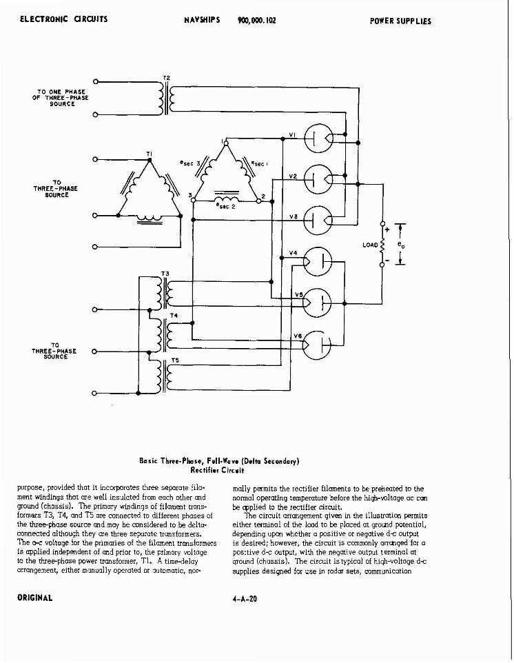
connected secondary) rectifier is extensively used where a large amount of power is required by the lmd, such as for large shipboard or shore electronic installations. The term thresphose refers to the primary a< source, whlch is the equivalent of three single-phase sources, each source supplying a sine-wove voltage 120 degrees out of phase with the others. Because of the three-phose transformer secondor, configuration, the cirmit i s sometimes ieierred to a s a bridge or slx.phose rectifier circult.
Inmony power-supply applications, it is desirable to provide two voltoges simultaneously-me voltage for hlgh- power stages ond the other voltage for low-power stages. For these opplicotions the threephose, full-wove rectifier circult con be mdified to supply on oddltional output voltage, which is equal to one half of the voltage provided by the full-wave rectifier clrcuit.

ELECTRONIC U R W l T S NAVWIPS w0.m. 102 POWER SUPPLIES
Circuit Op.mtion. The bosic threephase, full-wave rectifier circuit i s illustrated in the accompanying circuit schematic. The circuit uses a conventional threephase power transformer, T1, to step up the oltemoting source voltage to o high value in the wye-connected secmdmies. Tne primary windings of transformer T i are shown delta- cmnected, although in some instances the primary windings
L. 2 ,-- '-. - .k--- -. '..... ... a.* -..-.-.. , 2"uy 1_5 , T y - Y , l , l ~ , N ,"a ,"I U "a'-- "1 .--"I.= *,*LC I . . , . - he oiate of recufler Vi and t i e fiiament icathdej oi rectiiier '46 are connected to secondary terminal No. 1 oi transformer TI: the plate of rectifier V2 and the filament oi recuiier V4 are connected to secondary terminal No. 2: the piate of rectifier V3 and the filament oi rectifier V5 are connected to secondary terminal No. 3.
One f l lwent tiansiormer. T2, i s used to supply the 5 i a ~ e r . t ualtcge to rectifiers ) I ! , VZ. md '$3, since the filaments of these rectifiers ore all at the same potmtinl. However, since he filaments of rectifiers V4, V5, and V6 hove o high potential difference existing between them, mree separate iiiament transiormers iT3, -i4, ond T j i are used. A slngie fiiament transiormer may be used for this purpose, provided that it incorporates three separate fila- ment windings that are well insulated from each other and qround (chassis). The primary windings of filament trans- formers T3, T4, and T5 ore connected to different phases of the three-phose source. 'The a c voltoge far the pimories of the filament transformers i s ooolied indecendmt of, and . . prior to, the primary voltage to the threephase power t tonsfmer . T1. A timedelav arranaement, either manu- ally operated or automatic, n~rmally & n i t s the rectifier ,., ;:; 3x:n is cubr ;T&ru'r.? . - :.. .- 'kt. ... . , i . i . ~<! .. ,-,Wi"'Lq2 - iempi- atwe before the high-voitage ac can be appked to the rectifier circuit.
The circuit arrangement given in the illustratim permits either terminal of the loud to be placed at grouxd potential, depending upcn whether a positive or negative d c output i s desired; however, the circuit i s cmmmly arranged for a positive d c output, with the negative octput terminal at ground (chassis). The circuit i s typical of high-voltage d c supplies designed far use in radm sets, communication aonsmitters, or other equipment for which the d s pawer requuement i s several kilowatts or more.
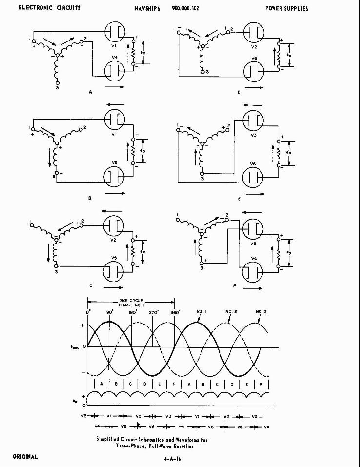
The operation of the three-phase, full-wave rectifier circuit c m be understmd from thesimplified circuit schematics (wtis A throuqh F) and the waveforms qivm in the occompyinq illustration. Tne basic three-phose.
full-wave rectifier schematic, given earlier in this discussion, has been simplified to show the d r d t action throughout the electrical c/cle; the reference designatims used correspond to those assigned in the baslc drcuit schematic.
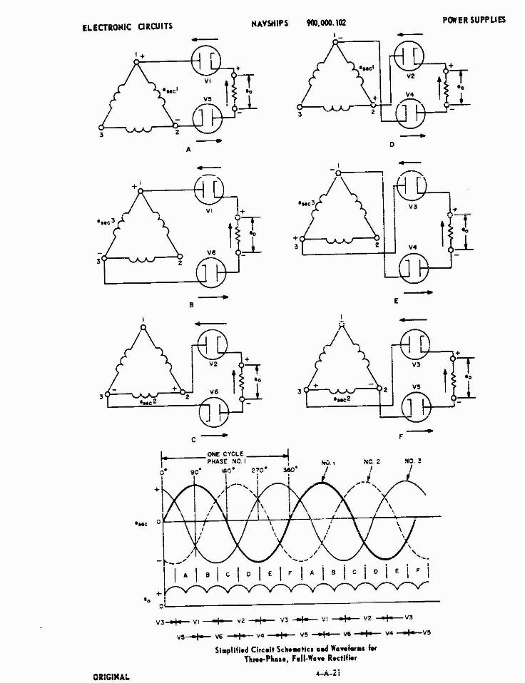
The voltages developed across the sffondmy windings of transformer Ti are 120 degrees out of phose with triutiort t" otki uie cor6hintiy ctnir1gL-~g i-2
poior~ty. iihe polarities indicated for the secmdaq wind- ings in the simplified circuit schematics (pats A though F ) of the accompying illustratim repesent the instantaneous palmity of the induced voltages in the s e e onday. The arrows on the schematics me used to indicate the directions of electron flaw in the circult.
The plotes of rectifiers Vl . V2, md V3 are cmnected to secondary windings No. I, No. 2 , and No. 3 , respectiveiy: the filaments (cathode) of rectifiers V6, V4, and V5, ore connected to s e c m d q windings NO. 1, NO. 2, and NO. 3, respectively. :%en the plates of V1, VZ, and V3 are posluve with respect to their iilamena, the rubes wiii canduct; whm the filaments of V4, V5, and VSme negorive with respect to their plates, these tubes will conduct. At any given instmt of time in the threephase, full-wove rectifier circult, a rectifier, the load, a d a second recti- fier ore in series across two of the wyecmec ted a m r former secondrnies and, therefore, two rectifiers ore con- ducting. Each of the six rectifiers conducts for 120 degrees of an electrical q c l e ; howeva, there i s an wer- lap of conductim periods, and the rectifiers conduct in a sequence which i s determined by the phasing of the ir:stc:;s2eG"6 seCx,?,=y 7~kCigeS G: tk,e W"ei tz::~~?:: in.the c t r ~ i t described, two r R t i f l ~ s me cmductIng at my instant of time, with rectiiler mn&cUon occurring in the following order: V1 md V4, V1 md V5, VZ and V5, V2 md V6, V3 a d V6, V3 md V4, V1 and V4, etc.
Ref= to the semdury-voltage wavefom, e.., shown in the accompanying illustmtlon. A s m e that the c-c wlt- cge induced in secondmy No. 1 (between 30 md 90 electrical degrees, phase No. 1) Is apprmching its mm- imum positive value (at 90 degrees); also, the voltage induced in secondmy No. 2 has reached its maximum neg- ative value (at 30 degrees) and i s decreasing. (Secmdary No. 3, olthmgh positive at 30 deqees, i s decreasing to zero.: This cmdition is shown by the simplified schematic of part A in the accompanyinq iliustmtim. ' h e plate of rectifier V1 bemmes psi t ive with respect to i ts filament
ORIGINAL
ELECTRONIC U R W l l S NAVWIPS WO,M)(1.102 POWER SUPPLIES
ORIGINAL
Simplified Circuit Schematics and Woveforms fol Three-Phase, Full-Wan Rectifier
(cathode), and the filwent of rectifier V4 i s negative with respect to i ts plate; therefore, b t h tubes conduct. and the elections flow thrw41, V4, the lwd, and V l fa 6 0 degrees of the electrical cycle.
In port 9, the a c voltage induced in secondmy No. 1 reaches i ts maximum positive value (ot 93 degees) and starts to decwase during the next 6 0 deipees of the cycle; the voltaqe induced in s e c o n d q No. 3 is apprwch. ing its maximum negative value. ?he plate of V1 remains positive with respect to its f i lwent , and the filament of V 5 becomes negotive with respect to i ts plate; therefore, V1 continues to cmduct and V5 takes over ccnduction frcm V4, with V1 and V5 conducting in series with the I d . Electrons flow through V5, the lwd, and V1 far another fin ~ P ~ ( P S nf the o(cle.
M part C, m e a-c voitoge induced in secondmy No. 3 reuches its maxiiiim, negative value and the ps i t ive volt- age in secondary No. 2 i s increasing. The filommt of Y5 :emails negctive with i ~ s p p ~ t to i ts plate? ond the plate of V2 becomes positive with respect to its filament; there iure, VS continues to conduct and V2 takes over conduction from V!, with VZ md VS conducting in series with the lmd. Electrons flow through VS, the imd, and VZ fa mother 60 degrees of the cycie.
in part D, the a c voltage induced in s e c a n d q No. 2 reaches i ts maximum positive value and starts to decrease; the voltage induced in seccndary No. 1 i s approaching its maximum negative value. The plate of V2 remains ps i t ive with respect to i t s fi lwent, ond thefilament of V6 becomes neqotive with respect to its plate; therefore, V2 continues to cmduct and \I6 takes we: ccnduction from Y5, wilh Vi and V6 conducting in series with the load. Electrons flow though V6, ttie l x d , m,d '$2 fzr another 50 d e ~ e e s of the cycle.
In part E, the a s voltage lnduced in secmdory No. 3 i s approaching its maximum positive d u e , and the negative voltaqe in s e c m d q No. ! i s deneasinq. m e filament of V6 remains negative with respect to i ts plate, and the plate of V3 hecomes positive with respect to i t s 'i!aent; therefcre, V6 cunwues to umdun md V3 takes over conduction from V2, with V 3 md V6 cunducting in s i e s with the I d . 3 e c : m s flow brn~gh V6, b e load, md V3 for another 60 degrees of the cycle.
In part F, the a s voltage induced in secmdcny No. 2 is upp imhk , j i:s mmi-LT neqctive vc!ce. and the positive ..-.,*- ,....,, e k ;,sec.~::d,~ ?<o. ? i s d ~ e c s i n g . 3 . e ?!ate of vl remains ps i t ive with r e s p : to i ts filmen!. znd the filament of V4 becomes neqative with respect to itsplate; L%erefore, 'v'j continues to cmdiict a d 'v4 takes over rondiirtion from V6, with V3 md V4 cmductinq in series -ii'~ Lhe lmd. El~-t-ons !low thou* V4, the lmd, and V7 for another 60 degrees of the q c l e .
The cycle oi operatlm 1s repeated, a s s h o w h port A, when the a-c voltage induced in s e c c n d q No. Z reaches i ts maximum negotive value and b e positive voltage in s~~-$.i:ary?:;. ! i; Y;c?xz!n;. ?.p fi!"mar! n! VA rmnins negotive with respect to its plate, m a the plate of i;i becomes psi t ive with respect to its fiimnent; therefore, V4 crr.5nces !n c;v.riiict and V! takes over cmducuon from . ." v. wici Vi on: '~'4 iii,:,itii.< in S Z ~ C ~ L?e !md.
WO.W0.102 POWER SUPPLIES
Electrons flow through V4, the lmd, and V1, to initiate another complete cycle.
Thus, from the action described abve, it can be seen that each positive and negative peok in each of the three phases produces a current pulse in the load. Becouse of the notwe of the rectifier conduction periods, each rectifier tube cor.ducts for 120 deqrees of the q c l e and carries one third of the total load current. I h e output voitage, e., pr* duced across the imd resistance i s determined by the instontmeous currents flowing through the lwd; thereiore, the output voltage has a pulsating waveform, which results in on irrequlatly shaped ripple voltage, because the output current and voltage ate not continuous. The frequency of the ripple voltage is six times the frequency of the a-c S C > J ~ P D S l n r ~ this r)??le f r ~ q ? l e n ~ / i s hioher than the ripple frequency of a smgie-pnase, fuii-wove rectifier cir- cult or a three-phase, half-wave rec:ifier c i r c i t , rslative!;. little filtering i s required to smooth out the ripple and pro- d:;;~ 3 steodv d% volt^^.
The threLphase, fuli-wave rectifier circuit makes continuous use of the transformer secondaries, with the d< load current passing through a s e c o n d q winding first in m e direction and then in the other; thus, there i s no tend- ency for the transformer core to become permanentiy mag- netized. Since little d-c core saturation o m u s , the effec- tive inductance of the transformer, and therefore the efiici- ency, i s relatively high.
The threephase, full-wave rectifier produces across the lood a pulsating (unfiltered) dT output voltqe, E,,, a s !nllnwa:
Em, = 2 . 2 E,. where: Em. = rms voltage across one secondary
winding ot three-phase Uansiormer 'The peak inverse roltog. across an individual rectifler
m the three-phase, full-wave rectifier circuit durinq the period of time the tube i s nonconducting i s approximately i.45 tlmes the rms voltage onoss the secondary wlnding of one phase. Some pulsating d s voltage i s always present onoss the load, ond this voltaqe i s in series with the appiled a-c secondary voiioge; therefore, the s u m of the :nstmtmwus pulsating d-c lood voltage and the instantan- mus p a k s e c o n d q voitoge represents the pea^ Inverse voltage across the rectifler tube. 3 e peak inverse voltoge per tub. can be expressed as:
El,, (per tubel = 2.45 Em. .nilcis: Em. z n.s voitaae across one semndoni
~
winding of the lhree-phasetransfomer - - - . 8 I .I_~ ,fir u u t p u ~ w i.ie ur i r r~ , ;se , :;!!-wove recti!ier :i:- cuii is cmneaed to a suitable filter circuit to smwth the ?"; scLmG < LLec[ ccr[a-ll Gs= ifl g-,e 1-d cir2-t, :yi!tei circuits are discussed in part Dot this section.)
A vorl,~rion ui he rilrephase, full-wave rectifier ci; ciir Gses :he ccmmm trrrr~;nai of he wye-cannected sec- ondaries and rectifiers V4, V5, and V6 to form a three phase, half-wave rectifier circuit. The circuit i s funda- mentally the same os tho! glven mriier; for this reason the iiccompmying citcdi: schemctic hos teen simplified and redrawn to ehminate the fi!amm,: t-onsformers md "E.FK!'~I%~ (ii?jnmenr C ~ ~ C I I I I ~ . ihe ~e1cienir. des i i~i~zt icr ,~ ~ ~ ~ " ~ ~ " ~ * y u>>*q,.=b ,Ci8,"~, U>,LL?~,~CL.
ORIGINAL
ELECTRONIC CIRCUITS NAVWIPS
v , L-A
Simplified Thmdbare, HalCWav. a d Thm-hot., Full-Wav. Rectifier Circuit
h e advantage of the circuit i s that two voltages m q be supplied from the same trmsformer and rectifier combino- tion. One output voltage (hut) i s obtoined from the full- wave circuit: the other voltage& which is equal to
7 . cne half of the full-wave output voltage, is obtoined using rectifiers V4, V5, and V6 and the mmmm terminal of the wye-connected seccndmies as a conventional three phase, half-wave rectifier circuit. (The opetatim of the threephase, half-wave rectifier circuit was previously described in this section.) Although this circui: variation con supply two output voltaqes simultaneously t o two sep- mate lwds, there i s a limitotion on the total w r e n t which canbe carried by the rectifiers (V4, V5, and V6).
W0,M)O. 102 POWER SUPPLIES
FAILURE ANALYSIS. No Output. In the three-phase, full-wove rectifier
circuit, the nwutput condiuon i s likely to be limited to the following possible causes: the lock oi a s filament or filommt-transformer primmy supply voltage, the lack of applied a s high voltage, or a shorted lood circuit (includ- ing shorted filter components).
A visual check of the dass-envelope rectifier tubes can easilv be mode to determine whether all f i lments are lit. The iilaments of V1, V2, and V3 should be ohserved first, because if these rectifiers are not lit there can be no d c output. If the filaments of V1, V2, and V3 ore not lit, the filament voltaae should be measured at the secondan, of transformer T2 to determine whether it i s present; if nec- essary, check the primcny voltage af T2 to determine whether i t i s present md a f themrrect value. If none of the rectifier filaments are lit, the primary voltage source for the operation of transformers T2, T3, T4, and T5 should be checked for the oresence of voltaae.
With the prim-ary voltage remov& from the circuit, continuity (resistance) measurements should be made of the s e c o n d 4 and primary windings to determine whether one or more windings me open. If necessary, the a s secondary voltage a t each of the three high-voltage s m d a r i e s m q te measured between the common terminal of the wye- nnvlected secondaries and the individual secondary ter- minal or the corresponding rectifier plate, to determine whether voltage i s present and of the correct value. Also, if necessary, measure the applied three-phase primary volt- age to determine whether it i s present and of the correct value.
With primary voltage removed from the rwtifier circuit, resistance measurements can be mode at the output ter- minals of the rectifier circuit (across load) to determine whether the load circuit, including the filter, i s shorted. A short in the components of the iilter circuit or in the lwd circuit will cause an excessive load current to flow. If the rectifier tubes me of the high-vacuum type, the hmvy Iwd current will cause the plate of the rectifiers to be- come heated and emit a reddish glow when the plate dissipotim i s exceeded and, if allowed to continue, may result in permanent damage to the tutes. If gas-filled rectifiers are used in the circuit, excessive lmd current will result in permanent damage to the tubes because gas- filled rectifiers me very susceptible to damage from cur- rent overlwd. Therefore, once the difficulty in the lwd circuit has teen located and corrected, the gas-filled rectifiers will require replacement a s a result of the over- Iwd condition.
Lo* Output. The rectifier tubes should be checked to determine whether the filaments are lit. Because of the normal overlap in rectifier conduction wriods and the cmduction of tubes in series to obtain full-wave outpit, one or more defective reclifiers in the three-phase, full-wave rectifin circuit con cause the low-outpit- condition. Fail- we of mly one rectifier in the circuit will cause a loss of rectifier conduction and no delivev of current to the lwd far approximately 120 deqees of the electrical cycle, and the output voltoge will be reduced accordingly. If rectifier tube V1, V2, or V3 i s not iit, the trouble is obviously
ORIGINAL
ELECTRONIC CIRCUITS N A V W I P S
associotd with the tube that 1s not lit since the filaments of these tubes are in poiallel; however, if V4, V 5 , or V6 i s not lit, then the trouble may be either the tube or its associated iilament supply (T3. T4, or T5). The tube fila- ment should be checked for continuity; the presence of mr- 1 s t fliament voltage 31 the tube socket should be deter- mined by mecsurement. If necessary, the primary and secondary voltages should be checked at the terminds o: die filament uansformer (T3, T4, or T5) to determine whether the transformer isdefective.
With the threephase piimory voltage removed from the circuit, continuity measurements should be made of the primary (ond secondmy) windmqs, to determine whether one (or more) of the windings i s open. I! necessary, the T; ~ , - i t n ~ - cf ~ n - i q ~ r n n d n r y hlnd!nn mav k meos~red between Vle comma, termlnai oi ule wyr comrcuu l und lilc ilidivlduol secondow ter;rc,c! or t i e corr:z~zdi~q rectif!er plate, to determme whether vcltage is pcsent und oi the correct ,vclue. *Is" I! nPcPssnry, rreos:ire 1b.e ap~ l>ed three-phose prlmmj voltaqe at each ? f t k phases, to drtrr- mine whether each voltaqe i s piesent ond of the correct value, since o low apF1:ed Fr:!rOry volto~e can result in a low secondmy voltoge.
Shorrej tur ,s ir elther the primcry or secondary wlnd~ inqs will cause the secondcry voltage to measure below normai. Cisconnect all secondary leads fro? the trans- iormer, TI, and measure !he current in each lea oi the three- phase prlmav wlth the transformer unloaded: excessive artmaw current is on lndlcation 01 sb,orted turns. A sec ondory wlnding wh~ch is shorted to the core can muse o !ow lilt^::! .ic!taqe :?d!ca!!@n: to determine whether a wind- ing is shorted to the core, oli leods should be disconnected kc- :he ~?2:>f3r!.e: =r:2 ,x zez?,.;:Cr.e?.! zcdc !lcv::ze?. egch individual wlndlnd snZ the ;ore, LS~:;; m o!~.reter or a ?.leqger (insulation tester).
Since a decrease m ioad resistonce con couse an :ncrecse :n liwd curer!! i!i,j pxsit , ly ;es;,l: i i n !m::~ output condition, the recnfieriiutp~t current (:o rb,e i~i ter circuit and to the load) shouid be check& to nrukr sure +L-, ; r 4 - , . . , t L , - +- e,rn,-- nnA eupacclve, " .> ~a . .~" ,... .-!
THREE-PHASE, F!JL?-WAYE !DELTA SECONOARY! RECTIFIER.
APPLICATION. .. . 8: ---r:,,:ie, ill!->;;.".; ;;,-.;';,-; :.:::b, +::- see. ,, .
u;iid:j ,b "d ,:. =:=-:: c; - . ;7 :7 . : f-; z;;!:Z!:-?,r *:?:P t i p nriri-?. <-c ;-;:;* is 1!.~e~--,k..3se id ti" i; ?..
o,~rct:t . ~ ~ w e r . ~ q + x e : ~ , e r ~ t > ~ I V i ~ h t , ~ s l ! >,,g:,. ':-:,e :<L::
f i - 7 CITC::I: :x !E nrrmced tc f ~ m ~ s h ether neqctive or ...:. :~.,:' .;!.-.i..::? . 11:f:: . .- 1'-" I.,?+.
CHARACTERISTICS. T.n,v &.,.. ,,, .- clrcui! ! s :tr~r-?i.c:e nc: ~u,?l!t ! s .ic w!!i
o ~ p l ~ t u d e of iippie voitcqi IFSS :/: 1:. !/mt icr c s~n.;!i- p,,u>r ;cm ,>,,=,.
WO,OM). 102 POWER SUPPLIES
Uses six high-vacuum or gos-iilied electron-tube dlcdes os rectifiers.
Cutput requires very 1:ttie filtering; d z output ripple frequency 1s equol to six times the pimory llne-voltage frequency.
Ucs g c d requiotlo~ chnractenstics. Citcult provldes ellher positive- or negative-polarity
07utpur voirape. Requires separote filament trcrstormers or separate
t~loner t ?wlnd~ngs for rectifier tubes. Uses multiphase power wonsfarmer with delta-connected
secandory .wlndmgs; primary windinqs may be either delto- o: iye-zannecti.ted.
CIRCUIT ANALYSIS. G e ~ r o l . 3 , e t+:ce-;tc:e, i~l!-a:.;c {ic!!c-c?zr.rc!e
s p r m i i n ~ l r~ct1lir.r 1s 3 variation oi the Cp,ree-phosc, fcil-wove (sin~lewye-connected s ~ o n d a i y ) rectifier, areviousiy described in thls section. The lull-wave recti- her with eelto secondaq i s USE? :vrere :: ;sr ,~e wnount oi power is requlred by the ioad, such as ior iuige ship bmrd or shore electronic instollotims. The term three-
phase reiers to the primary i?- source, which is the equi- .u!cr: 2f three single-phase sources, each sourc? supply- inq a sinewave volfoge 120 degrees out of phase with the o:b,ers.
Circuit Oparo+lon. The three-phose, full-wave (delta secondwj) rectifier circuit 1s illustrated in the accompany- ino clicuit schematic. ?he circuit uses a three-chase power wansformer, TI , to step up the alternating source vuituqt to o hlqh io1ue iii i h i ielic-cmiciii.: ~?~>:id;~lts_
Each secondary w~nding is connected to the other in proper : h e rn!n!ionchip cn tho1 the nlrrents through the wind- ir2s ore ixllwced. 3amage ran result to the tonsformer windings if improperly connected; for *,is :eason, tke windinqs ore usually cmneaed mtemolly ir. the proper rhcse t? 2revmt the pnssib!lit~ of nokinq wronq connec- tions, nnd only the three secindory terminal; arc k q h t cut ~f ti,e case. .-
~ n e primary wlndlngs of trmsiormer T i are shown d e b connected, although in some mstmces they moy be wye- mnnwtpi. (as for c threr- or four-wlre system).
~ ' R P c!c!e 3f re~!!!~er V1 ondthe illament (ccth&ej of rectiflei V4 ore connected to secondary termino: Ni. I of r r -n- f - rm~r T i : t h e plate of rectlfler V 1 ond the filament of :%!:!it: "5 .re cnncec!~d In s e r o n d n q tprrninal No. 2: :'r p!3:e c! yp~!::!pl ' V i nn"i"n i!innprt r.: i r r ~ i i i r i 'ib ~ T P ?on:~c!ec !L- ii-c?naxy tirninni No. i.
- r e I . ,..~....... l.-rrrrr..., TL, I S ,JSP?, !O s ipp ly i r e 1i;i:-
mpnt voltone to iectii!ers V1. VS, ond V3, since the iiio- m?rT+ ni V b p . 0 ?-CI,+I-FS ~ T P o i l at t n r slinse mter,llo;. fici\.-ver, since the fl!aments oi rectifiers V 4 , V5, acd Vb l~agc d hiqk, )cta;tid :.f!c>:r.cc ?x.st::,:; x?:vcec !her, *,Fee separnte i!lm.ent rronsiormers i 'r3, T4, unb 75) aie csed. A s i n q l ~ fiioment t~msiorrer r.ay De used iar this
ORIGINAL
NAVWIPS WO.OW.102
o z O T ~ ~ ~ E ! ~ z ~ E SOURCE d l L p
10 THREE-PHASE
SWRCE
TO THREE-PHASE
SOURCE
Basic Threr-Pbre, Full-Wove (Delm Secondary) Rectifier Circuit
POWER SUPPLIES
purpose, provided thot it incorporates three separate fila- ment windings thot are well insulated from each other and ground (chassis). The primory windings of filament trans- formers T3, T4, and T5 are connected to different phases of the threephase source and may be considered to be delta- connected although they are three separate transformers. The a-c voltage for the primaries of the filament transformers i s applied independent of and prior to, the primory voltage to the threephase power transformer, TI. A timedelay arrangement, either monuolly operated or automotic, nor-
mally permits the rectifier filmnents to be preheated to the normal operating temperature before the high-wltage oc crm be applied to the rectifier circuit.
The circuit arrmgement given in the illusuatian permits either terminal of the l a d to be placed at ground potential, depending upm whether o positive or negative d c output is desired; however, the circuit is commonly arranged for a positive d c output, with the negative output terminal at qround (chassis). The circuit istypical of high-voltage d c supplies designed for use in radar sets, mmmunication
ORIGINAL 4-A-20
ELECTRONIC CIRCUITS NAVWIPS WO.OW.102 POWER SUPPLIES
transmitters, or other equipment for whlch the d i pwer requirement i s several kilowatts or more.
The operotion of the three-phase, full-wave rectifier circuit can be understood from the simplif~ed circuit schematics (ports A through F) and the waveforms @en in the accompanying illustration. The b s l c three-phase, full-wave rectif~er schematic, given earlier in this dis- cussion, has hem simplified to show the circuit action throughout the electrical cycle; the reference des~qnations used correspond to those assigned in the b s ~ c circuit schemat~c.
Tne operotion of the delta-secondary rectifier circuit i s similar to that of the we-secondary rectifier clrcult (previously described); however, the a-c voltage across an individual deltoconnected secondary winding 1s 0.742 E,,, whereas the voltoge ocross on individual wye- connected secondory winding is 0.428 E,, (E,, i s the unfiltered d c output ocloss the load). The valtaqes developed across the secondow wlndings of transformer T I ore 120 degrees out of phase with relation to each other and ore constantly changing ir polarity. In the delta-connected secondary, a t any given instant the voltoqe in one phase i s equal to the vector sum of the voltages in the other two phases. The polarities indicated for the secondory wind- ings in the simplified circu~t schematics (pa t s A through F) of the occompnying illustrotion represent the inston- taneous polarity of theinduced voltages in thesecondary. Although the instantaneous polarity shown in heschemotic i s @ven for only one sffondcq winding, the sum of the instantaneous voltoges in the other two windings i s equal to the ~ l t o q e oi the first wirdlng. The arrows on the schematics are used to indicate the directions of electron flow in the drmit .
The plates of rectifiers V1, V2, and V3 ore connected to secondan, terminals No. 1. No. 2, end No. 3, resDec- tively; the filaments (cathodk) of rectifiers V4, ~ 5 , m d V6 me mnnected to secondarv terminals No. 1. No. 2, and No. 3, respectively. When th; plates of V1. VZ, and ~3 are positive with respect to their filaments, the tubes will conduct; when the filaments of V4, V5, md V6 are negative with respect to their plates, these tubes will conduct.
At my qiven instant of time in the threephase, full- wave rectifier circuit, a retifier, the load, ond a second rectifier are in series across two terminols of the delta- connected secondaries and, therefore, two rectifiers ore conducting. Each of the six rectifiers conducts for 120 degrees of an electrical cycle; however, there i s m overlop of conduction periods, and the rectifiers conduct in a se- quence which is determined by the phasing of theinstantan- eous secondary voltages of the power tronsformer. In the circuit described, two rectifiers are conducting at any in- stant of time, with the rectifier conduction periods occurring in the following order: Vl and V6, V6 and V2, V2 and V4, V4 and V3. V3 and V5, V5 ond V1, V1 and V6, etc.
Refer to the secondary-voltage waveform, e..,, shorn in the accompanying illustrotim. Assume that the a-c voltoge induced in semndary No. 1, transformer terminals No. 1 and No. 2, i s approaching its moximum positive value (at 90 degrees); also, the voltage induced in secondary No. 2, tronsformer secondory terminals No. 2 and No. 3, has
reached its maximum negotive value (ot M degrees) cnd is decreasing. (The voltaqe induced in secondoy No. 3, terminals No. 1 and No. 3, i s possing throuqh zero.) This condition i s shown by the simplified schematic of port A in the accompanying illustration. The plate of rectifier V1 is positive with respect to i ts filament (cathode), and the filoment of rectifier V5 is neqative with respect to rts plate; therefore. b l h tubes conduct, and electrons flow through V5, the load, andV1 for 60 degrees of the electric01 cycle.
In port B, the o-c voltoqe induced in secondarv No. 1 hos reoched i ts moximum positive value (at 90 debiees) and starts to decrease durinq the next 60 devees of the cycle; the wltoge induced in secondory No. 3 i s approach- inq its maximum neqative value. The plate of Vl remains positive with respect to its filament, ond the iilament of V6 becomes neqotive with respect to i ts plote; therefore, Vl continues to conduct and '$6 tokes over conduction from V5, with V1 and V6 conducting in series with the lood. Electrons flow through V6, theload, md V1 for another 60 degrees of the cycle.
In part C, the G-C voltage induced in secondary No. 3 has reached its moximum negative value and storts to d e crease; the voltage induced in secondory No. 2 is approach- ing its maximum positive volue. R e filament of V6 r e mains negative with respect to i t s plate, and the plote of V2 becomes positive with respect to i ts filoment; therefore, V6 continues to conduct and V2 takes over mnduction from V1, with V2 mdV6 conductin? in series with the lood. Electrons flow through V6, the load, andV2 for another 60 degrees of the cycle.
In port D, the o-c voltage induced in secondary No. 2 has reached its maximum positive value and starts to d e crease; the voltage induced in secondary No. 1 is opproach- ing its moximum negative value. The plote of V2 remains positive with respect to its filament, md the iilament of V4 becomes negotive with respect to its plote; therefore, V 2 continues to conduct and V4 tokes over conduction from V6, with V2 and V4 conducting In series with the lood. Electrons flow through V4, the load, and V2 for mother 60 degrees of the cycle.
ln part E, the a-c voltoge induced in secondory No. 3 wprooches i ts moximum positive volue, and the negotive vcltoqe in secondary No. I i s decreasing. ?he filament of V4 remains negotive with respect to i ts plate, and the plote of V3 becomes positive with respect to its filoment; therefore, V4 continues to conduct and V3 takes over con- duction from V2 with V3 and V4 conducting in series with the lood. Electrons flow through V4, the loo?, md V3 for another 60 degrees of the q c l e .
In part F, the o-c voltage induced in seccndary No. 2 approaches i ts maximum negative voiue, and the positive voltoge in secondory No. 3 i s decreasing. Tne plote of V3 remains positive with respect to its filament, and the filament of V5 becomes negative with respect to its plate; therefore, V3 continues to conduct and V5 takes over mn- duction from V4, with V3 and V5 conducting in series with the load. Electrons flow through V5, the load, and V3 for another 60 degrees of the cycle.
Tne cycle of operation i s repeated, a s shown in part A, when the c-c voltoge induced in secondary No. 2 hos
ORIGINAL
ELECTRONIC URCUITS NAVWIPS
reached its maximum negative value and the positive voltage in semndary No. i is increasing. The filament of V5 r e mains negative with respect to its plate, and the plateof V1 becomes positive with respect to its filoment; therefore, V5 mntinues to mnduct and Vl takes over conduction hom V3, with V1 md V5 conducting in series with the load. Electrons flow through V5, the lood, md Vl, to initiate mother mmplet? cyclr.
Thus, from the anion described above, it c m be seen that each positive md negative peck m e a h of the lhree phases produces a current pulse in the load Because of the nature of the rectifier conduaion periods, each rectifier tube mnduds for 120 degrees of the cycle and cmies one third of the total load current. n i e output voltage, eo. phF -'..--A ---- .Lo I--.' .~.io",,, i , d~taminpr i the in- -"--" ".- .--- ~
stantmmus cunmt flowing throum the ioao; mereiore, ine output voltage has a puisdng woveform, whid results in M lnegdmly doped ripple voltage, because the output , ~ ~ x e i i t md vo!;nqe arc act mrtinucus f r e ~ e n c y of the riwie voltaae i s six tlmes the frearenn, of the u c source, . . Since this ripple frequency i s higher thm the ripple frequency of o s n a i e ~ h a s e , full-wove rectifier circuit or a threeohase. . . . holf-wave rectifier circuit, relatively iittie filtering i s rewired to smooth out the rlmle and ~mduce a s w d v d-c . . voltage.
The threwhase, full-wave reaifier drnrit mckes con- tinuous use of the trslsformer semndmies, with the &c load current possina throuqh the deltc-mnnected semndaw windings fir; in on; direcfion and then in the other; thus,. there is no tendenq lor the trmsformer core to become permanently mopetized. Since littie 6 c care saturation occurs, the effective inductonce of the trmsformer, and there fore h e eificieni), is ie1ative:Y :ii:l:... The threeohase, full-wave redf ier with deltceonnectd semndaries produces a m s s the load a pulmtotlng (unfriteredj &c output voltoge, E,., a s follows:
E., = 1.35 Em, where: Em. = ms voltage across one secondary
w~nding of lhree-phase delta-connected ?ronrfomer
The ~nrerse v01t.g~ acmsc an individual rectiiier in ;$e ;$ieephse, !dl-ware cirad! &r?cg Che period oi time the !"be i s nonconducting i s approamotely 1.42 times the rms wltoge m o s s the secondary mnmng of one phase. k r , e p d s k n &c ,.:o!tsge is d s z y s ::.sent wmsa the :>&. .. . :r:! t::i. i r l l l .2~ i s in .w?,r; .with Ii? ~?0!i& 5%
sc-;rn&rv wliqs; 'isiefi;c. :he :- c! !he i ? s t z ! ~ - ~ , s sulsatino k lood \olt,z:e x.2 L?e instmtmecus peak peak semndary vulto,qe repiesa.:; :'.e 2eak :?.'verse vo:!a;e zcross the rectliier tube. The penk inverse voltage par tubs --- L . ",. .,c ?x;:cs:d as:
E,,, (per abe) = 1.42 Em, where: Em, = ms voitugr ociuss uzt sc;ji.d;-j
xln0ing of three-pnose deiio-cur~neied !mnsfomier
Th: z~tp;! s! 'hn Lki-phh-, f n l l - w n v ~ r en i f i e~ CIT- cult i s connected to a suitable iiiter circuit, to smauth the ya!smicq direa mrte,! for use in the l o d ccl~cuii. (Ti:- I", ,-;.,-,,:,- --- >:--.--- ' i- --.. ? -',h,* sei~.fjm ) ._.._.._. I,,- ..lsI.,I.l*L" I.. "l. L _ ". ".._
POWER SUPPLIES
FAILURE ANALYSIS. No Output. In the three-phase, full-wave (ddta semn-
day) rectifier circuit, the nwutput mndition i s likely to be limited to the following possible m u s e s the lock of a-c filommt or filanent-transformer primary supply wltoge, the lack of applied o-c h?gh voitage, or a shoried iwd circuit (including Aorted filter components). -. . ,
LnecKs lor r a i i i i a iubr wid f;:iu7reri: t-u?sforzx Gpe- lion md for a +torled load circuit are the m e as those given for the hee-phase. full-waveisinale "Y" secondare) rectifier circuit, previously described inihis section.
.
With the primary voltoge removed from the circuit, mn- tinwty (resistance) measlranents douid be mode af the secondary and primary windings IO determine whether one or more windings ore o p n . Since the three windings of the A :.- - - ~ . . ~ ~ e c : i . & ~ i ~i:z;i! T e -meti-rs m z n e o 6 Lntwnaiiy md only three terminals me brouqht out of the case, voltage oxd resistance meosu:ements ore made betwm. the terminals oi the deltucannected semndories. hben making measure ments (witage or res~stoncej oi the secmdary citcuir, it should De rememoerea inai ine windings form o delta mn- figuration, with two windings in series and this mmbino- tian in w a l l e l with the winding under mmsurmmt. In other instances, the semndmy windings me mnnmed to six individual lerminols. m d these t&ninals are connected to- gether to form a delta configordon. n u s , in this in- stmce, the terminal mnect ions may be removed to enable m m s w w m t s to be mode on individual semndary windings indep~ldent of other windings. If necessmy, the uc second- ary voltage at each of the t h e e high-voltage seoonb ies n q * meosv:rd &iWe*~: *:e ie-inol; -f the dc!:c=Jn- nected semndaries, to determine whether voltage is present a d of the mrrmt value. Also, if n e c e s s q , measure the applled threephase pr!maq wltoge to determine whether :i is present md of lhe mrrer! value.
L o r Ouwt. Except for the voltage and redstance measurements of the deltc-sewndmy circuit, the checks for !owoutput mndition ore t!!e sane as lhose @ v a ior the three-phase, full-wave (single "Y" s e m o d q l reaifier drcuit, previously discussed in this section. Also, refer to the pagraph above tor lniormation mncemlng procedures to be used h e n making voitcge md resistonce mwsu;ements on delta-connected seccndary ?nndinqs.
THREE-PHASE, HALF-WAVE (DOUBLE "r" SECONDARY) RECTIFIER.
APPLICATION. - - - : L ~ ,*;c <s,, -;,"*, “ ~ : - " ~ ; c :ec;j!;c *:?!*.A";:
smndmy md m t e ~ h o s e ieccroi i s useJ in rlciiofii i s,&:,; ,,=:, :"; +,i: -;..-..; ..,:,,;,= "; - - ' - ~. , - . . . .. - . . . :. . . . . . . .-Tee- ..- pnose m c :nr 6 c uuipul p r e i ieqqd;a7aiib are :i :, ,; ire:, :,;,7:,. -- - --.. ' -.-.:. -- k. "..""-,-' r , ' , ,-i& . . / o r ,C%II.LLI -..- ".. I. ..
iii-si T1E.;.~ii.? :i ?.;:i::.:e j:~:5-..2j:":~ ,:;:w: tJ 'LL I??,! .
CHARACTERISTICS. input to cira~?ilt i s threephcse or: output 1s ac w~Vl w-
;i!!-de r! ri:?!e w!!age iirrs !hap tho! 'iii 0 sinolwhase TS.C.!fiB.
ORIGINAL
ELEClROHlC CIRCUITS NAVWIPS
Uses six hi&-vacuum or gos-filled electtowtube diodes as r e d f i a s
Output requires v q little filtering; &c output ripple f r ~ m c y is epud to six times the primlny linevoltage fre QJencv.
ti& gmd regulat~on cnmacterlnics. Clraut provides ether p v t l v e or negative-polor!ty
output wltage. Replires only one filmmt-voltage mpply. Uses multi~hase wwer transformer with two oarallel sets
of wyeconneaed &ondaries operating 180 deGees out of ~hase with each other. Tne center mints of the weson- nened secondaries ate mnnected through m inte&ase reccfor or balance coil to the locd. The primacy windings are generally deltc-mnnected.
CIRCUIT ANALYSIS. G*r.nl. FundamentaUv. this rectifier circuit resembles
two half-wave (threephase';tarl rectifiers in wallel, wch ratifier circuit operating from o mmman deltc-mnnected Primmy, md sharing o common lcad through m interphase reactor or b a l m mil. (Tne three-phase, half-wave r d f i e r drcuit was previously described in thissection.) The threephase, half-wave (double-wye smndmy) tecti- fia circuit uses a power uansfomer with two sets of wye- m ~ e c t e d secondaries, the windinas of m e set beinu con- neaed 180 degrees out of phase with respect to the &r reqmding wlndlngs of the other set. For this reason, the circuit issometimes referred to as a six-phes. rectifier. Tne Junction paint of eoch wye-mnnected sewmdlny is, in turn, c o n n e d to a center-tapped inductance, called an lnwphas. r.ener or baleas. all. 'The center tap of the interphase reactor i s the wmmm negatlve terminal for the l o d
900.000.102 POWER SUPPLIES
Circuit 0p.mtion. ' he threephase, half-wove (double wye secondary) rectifier circuit is illustrated in the qccom- pnying circuit schemtic. The circuit used a three-phose power trmsformer, Ti, to step up the alternating source wltaqe to a high d u e in the wyeconnened secondaries. The prluary windings of trmsformer T1 are shown delta- mnnected; the delta primary is common to toth wye-mn- nected secondaries. The plates of rectifiers Vl, V2, md V3 are mnnected to one set of smndary ("A") windings at tmlnals IA, 2A, and 3A, respectively. Tne platesof rectifiers V4, V5, and V6 me connected to the other set of secatdary ("8") windings at terminals 38, 18, md 28, respectively.
One filmmt transformer, T2, is used to supply the filo- ment wltage to all retifiers, since the filament of the rec tifiers me all at the sane potential. Although a single filammt trmsformer is Shown MI the schenaic, as mmy as three identical filwent umsformers are sometimes used as the filmmt supply, with each filament transformer su~plVin~ twa for more) rectifier Nbes: in thismse the .. . - primary of each singlephase filwent transformer is mn- nected to a different ~hase of the three-uhase source. Voltage isapplied ta'the primaries ofthi filment trans formers before it is opplied to the primary of the three phase power transformer TI. A timedelay arrmgement, either manually operated or automatic, normally permits the rectifier filaments to be preheated to the normal operating temperature before thehi&-voltage ac cm beapplied to the rectifier drcllit.
The center-trpped inductmce, L1, is an interphase r e o r Or bolance mil. Tne mmmon termind of each w y e mnnected sffondmy is mnnened to one md of L1; the
ORIGINAL
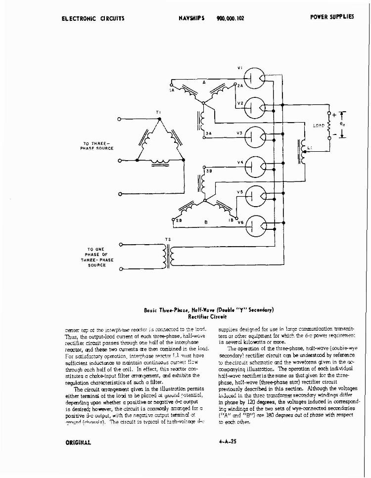
ELECTRONIC CIRCUITS
TO T H R E E - P U I C F F O U R C E
T O ONE PHASE O F
T H R E E - PHASE S O U R C E
Basic ThrrcPhss, Half-Wa*. (Double "Y" S*co~dory) Rectifi., Circuit
POWER SUPPLIES
cenre: t q a1 me lnrerpnase iem:c; is ;onr.~:ed ro iocd. D,us, the output-lwd current of earn threephase, half-wave ;ectifier 3;riiit passes through one half of the iniffphase ;emtor, md these two curients me m a mmb~ned in h e iwd. Fo; sotisfocto;y opm-,:ion, interphase ienctoi 1.1 must have sufficient mductmoe to niaintun continuous current flaw rhiough each hho of the mil. In effect, this remor con- stitutes o choke-input filter awmgement, old exhibits the regulation darccteristics of such a filter.
The circuit arrangement given in the illustration permits either terminal o! the i o n m be piaced ai gwuid ?>ienil':d, deoendina uwn whether a msitive or netptive d i output . . Is'desired; hawwer, the circuit i s comrmdy arrmged for a msirive bc oui0~i. wii?, bL,e ~ e ; c . ~ c o-:p-! !mild n_!
ters or other equipment far whlch the d-c power requ?remen! i s several kilormtts or mare.
'he operotion of the rkeephase, hd!-wave (double-ye secondary) rectifier circuit c m be understcod by reference !o theiirctA: whemctic and the waveforms given in the oc- companying illustralion. m e operation of each individual holf-wave rfftif!eristhesme as thatgiven for the three phase, half-wave (threephase star) rectifier cirarit previously described in this s d m . Although the voltages
- 1 A - .'-At..* ..l.."4^.."acomnAm .,,i",i!"m differ " l U Y C N ,I, "1s u r r r c ..-. -.- in phase by 120 degrees, the mltapes induced in correspond- ing windings of the two sets of wyeconnected secondaries [''P." m.! "E"! ore 180 d q e e s out of phase with respect L" d! other.
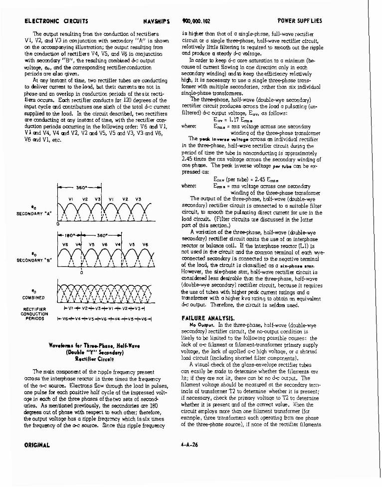
~,000.lm POWER SUPFLAS
The output r e d t i n g from the mnduction of rectifiers V1, V2, and V3 in conjunction with semndary "A" i s shown on the ccwrnpmvina illustration: the outout resultina from the conduction of r&ifiers V4, VS, and ii6 in mnjunnion with s ~ a n d r n v "B", the remltino combined d-c o u t ~ u t wltoge, 6-0, and the corresponding rectifiermndunion periods are als, d v m .
At any instancof time, two rectifier tubes ore conducting to deliver current to the bod, k t their axrentsore not in phase and an overlap in conduction periods of thesix recti- f i ~ s occurs. E d rectifier conducts for 120 deqrees of the input cycle m d mtr ibutues one sixth of the total & current supplied to the load. In the circuit described, two rectifiers me mnductlng a t any instant of time, with the rfftifier mn- dudon periods w i n g in the following order: V6 m d VI,
md V4, V4 md VZ, V2 and V5, V5 md V3, V3 and V6, V6 md V1, etc.
=o COMBINED
RECTl FlER + V l 4 V 2 t V 3 4 - V l 4 V 2 4 - V 3 4 CONOUCTMN
PERIODS l r V 6 3 - V 4 + V 5 4 V 6 4 V 4 4 V 5 + V 6 1
Wavebms for Thn*Pbns., HaICWav* (Double "Y" kmndnry)
R*ctifi.r Circait
The main m m p n m t of the rlpple frequenq present actoss the interphase reactor i s three times the freplency of the a-c SOWE. Elecums flow thmugh the load in pulses. one pulse for each positive half cycle of the impressed volt- age in each of the three phases of thetwo sets of second mies. As mentioned previously, the secondaries me 180 dearees out of ~ h a s e with reswct to each other: herefore. theoutput voltage has a ripple frequmcy which'issix timis the frequency of the o-c source. Since this ripple frequency
is hi*er than that of a singlephase, full-wave ren i f i a circuit at o single threephase, half-wave rectifier circuit, relatively little filleting is required to smwth out the ripple and prodce a steady b c wltage.
In order to keep d-c mre saturation to a minimun [be c a s e of current tiowing in one direction only in ead, semdary windins) mdto keeo theeffidmor relativelv hi&, it i s necessmy to use oi ingle three-pkase trans: former with multiple secondaries, rather than six individual singlephase transformers.
?he threephase, half-wave (doub leye s e w n d q ) rectifier circuit pmduces m o s s the Iood a pulsating (un- filtered) &c output voltage, E,,, a s follows:
E, = 1.17 Em. where: Em. = nns voltage across one smndary
winding of the threephose transformer The p d Inms. *oltop. across m individual rectifier
in the threephme, half-wave rectifier cirmit during the period of time the tube is nonmnductinq i s approximately 2.45 times the rms voltoge across the secondary windinq of one phase. The peok inverse voltage per tube can be ei- pressed as:
Em, (per t u k l = 2.45 Em. where: Em. = rms voltage acmss one smndorv
winding o i the three-phase tmnsformer The output of the threephase, half-nave (double-vrje
sffondow) rectifier arcuit i s mnnected to o suitable filter circuit, to snooth the pulsating direct current for use in the load circult. (Filter circuits are discussed In the latter pan of this section.)
A vmiaion of the threephase, half-wave ( b u b l e - y e semndmyl rectifier arcuit omits the use of m interphase reactor or balance coil. If the interphase reactor (Ll) i s not used in the drcuit and the mmmon terminal of e& vr je
mnnected semndory is connected to thenegative terminal of the load, the arcuit i s classified a s a SIX-phase s ~ r . However, the six-phase star, half-wave rectifier citmit i s mnsidered less desirable thm the threephase, half-wave (doublewye secondary) rectifier circuit, becmse it requires the use of tubes with higher pe& current ratings and a trmsformer with a higher kvo rating to obtain m equivalent k output. Therefore, the circuit i s selbm used.
FAILURE ANALYSIS. No Output. In the threephose, half-wave (doublewye
secondary) rectifier circuit, the no-autput condition is likely to be limited to the foliowing possible causes: the lack of a c filament or filoment-tansformer primary supply voltage, the lack of applied a c high voltaqe, or a shorted lmd circuit (including shorted filter components).
A visuai check of the glass+nvelope rectifier tubes can easily be made to determine whether the fiiaments are lit; if they me not lit, there can be no d c output. The filoment voltage should be measured at the secondary term- inals of transformer T2 to determine whether it is present; if necessary, check the primary voltage to R ta determine whether it is present and of the correct value. When the circuit employs more than one filament trunsformer (for example, three transformers each operating born one phase of the three-phase source), if none of the rectifier filaments
ORIGINAL
ELECTRONIC CIRCUITS NAVWIPS
are lit the primory voltoge source for the f~laaent trons- formers should be checked for the presence of voltoge.
With the primary voltage removed from the circuit. continuity (res~stance) measurements should be made of the secondary and primary windings, to determine whether one or more windings are own md whether :he cammor, term- lnols of the veconnected secondaries are connected to the Imd clrcuit thrauqh the interphase reactor or baiance coil. If necessav, the secondw voltaoe mov be measured . . ot one (or morel of the high-voltage secondaries between the common terminal of the weconnected secondaries md c secondary terminal or corresponding rectif~er plate. to determine whether voltoge is present and of the correct value. Also, if necessary, measure the applied threephase
--I+--- +- .'dmnlnn .whether i t IS oresent and 01 w,, , , . "., ."..""- .- ...- ~~
the c o A t v iue . With primory voituqe reiicved irom :he :ec!:!!er cirau!!.
resistance meusurements can be made at the c~ tpu t term- !nais of !hc ;cc:if:er circuit !ncmss lmll to determine wh~ther the lwd circu~t, lncludlng the filter, 1s shorted. A short in the conponents of the filter circuit or in the imd circuit will cause an excessive lcad current to flow, md the full output voltoqe will be developtd across each hali oi the lnterphase reactor, Ll . If (he rectifier tubes ore of the high-vaciiwr; t y p , the heavy lmd current will came the plates of the r ec t~ f~er s to become heated and emit a reddish glow when the plate dlsslpation is exceeded and, i f allow- ed to continue, may result in permanent damage to the tubes. If gas-filled rectif~ers ore used in the circuit, excessive imd current will result in permanent damage to the tubes because gos-filled rectifiers are very susc-pribie lo dumoge from current overload. Therefore, once the difficulty in the I& , ..rcui: -. i?35 krr: :x i ied ~ n ? . ~crrcct&, t?" qas - f~ l i~d rectliters wlli require reaiocernen: us 3 r e s ~ l t of tlle 3VeI-
Imd condition. Low Output. Tne rectifier tubes should be checked
to determine ,whc<m.e: ail filamei,ts 1715 lit; I.owever, becailse of the normal overlap in rectifier conduction priods, the failure d o n e or two rectlf~ers in the circuit will not cjre;:l,y affect the ~u!pilt vnltnqr hut may Increase the ripple ompiitude. If o ~ l y one rectifier is not lit, the tube filament sbouid i*. c ~ - - ~ . i n & e u i 4 - .,, ---.:-,,i,., L,..~ ......,. !f !he nrcoit rmoioys i ro~c 15.3" 0p.e filament tronslamer and one or more tubes are not lit, the corresponding filament transformer (sl shouid ce checked. Measure t'e se=cda?j vcltoge to 5etir:I-e ;;.kc:!e: t?,? cmr.ci fi!nm~n! r,c!!aqe is Dresent: the orlmaiy vcicuijr she^;.! ke zeosxei: 3!:?.e trncsfmrnrr !-rmlnols, to determine whether valtoge 1s opp!~ed 3nd oi :he correct value. lf necessary, iontiniily ne-sxeme-1s o! !'-:e tma"s!ori;~r ,w>ndinos should be madp to determine nhe<hei the tl~.s!7i7~1 i: ?C!CC!:VC.
The continultv of each holf cf the lntrrphcse reactcx, LI, should be measurea to deterri.irir whether one t,di ;: the winding i s open. An open circuit in one hoii of this reonor w ~ i l & s c o r m t its assoc~nted three-ut,ase, ,we- mnneted secondury, til= I~YI*: .;~!:igc ,::ill ? s c r s s e EC n
result, m d l h e r ~ t i f i e r circrat will continue to operate as o inreeph~se, hdf-wave ;ec,i!:e: wi!h single-*ye secondw. . . :k:!h t?n: tb:eeqh+ lrixcry Y C ! : ~ ~ E r e~cved ~ T O C , tile c z c ~ i t , ca.?t:?vi!y r r ~ ~ c ~ ~ t ~ ~ t ~ ~ ~ . e ; ~ ? ~ sI,c<!i !x zc<e s! !he
WO.WO.102 POWER SUPPLIES
,rimary (md secondary1 windings, to determine whether one (or mcre) of the windings i s open. If necessaq, the a c voltage of each secondmy winding in each set of secondaries may be measured between the common term- inal of the wye connection and the individual secondary terminal or the correspond~ng rectifier plate, tc determine whether voltage is p e s m t and of the correct vaiue. Also, ii n e n a s u y , iil6jYre LLle applied L?:ee-$,as. primnry voltaqe at each 6hase, to determine wt~elher vo!:age is present and of the correct value, since a low applied primor/ voltage can result in o low secondary voltage.
Shorted turns in either the primary or secondary windings nil1 cause the secondary voltoge to measure below normal. Disconnect all secondary leods from the uans- former, and measure the current in each les of the three ph;se p i a z y with :he lransform?r unioo6e6; excessive primow current i s on indication of shorted turns. A secon- dary winding which is shorted to the core c m also cause o low output voltoge indication; to determine whether a winding i s shorteato the core, all leads shouid br disi>nneste3 from the transformer and a measurement made ktweer; ffic!: winding and the core, using an ohmmeter or a Megger (in- sularion tester).
Since a decrease in iood resistance can cause M
lncreose in lcad current and possibly result in a lownutput condition, the rectifiernutput current (to the filter circuit ond to the lwd) should be checked, to make sure thot it is within tolerance and i s not excessive.
HALF-WAVE VOLTAGE DOUBLER.
APPLICATION. The holf-wove voltagedoubler circuit is used to pro-
duce o hlqher d s output voitoge than con be obtumk from a conventions1 half-wove rectifier circuit. Tnis volt- age doubler i s noimolly used in "transformerless" circuits where the iood current i s small and voitoge regulation i s not criticcl. The circui! is frequently employed a s the power supply in smoll portable receivers and audio amplifiers and, in some transmitter applications, as a bias supply.
CHARACTERISTICS. Input to circuit is oc: output is puisating dc. U s output voitoge is approxinlately twice thot chained
from equivalent half-wove rectifier circuit: output current i s relatively smoll.
CII~CY: i e q u ~ e s i:j:er:>;; 4-: , 28Jcpu~ jii,:j:? :~+:q,.e:,c, is uquI to c-i source f;eql;enq.
-~ i l ~ a +ur ;t~~;zG:i. C~,G;ZC:E:;;::CE; ~.c.:t;'it v"!fwr 3~
ovaiiable i s o iunctim of load cuzrent. - , . . -,eLmLL?a ";";; ;;)C>;t z;;:;-zt:z:z, -,:y + ,>5e4 dtk:
or wlthout 3 power lsulatlan ironstoimei. G a t s indirh-tly heated co','.ode-!ype rectifiers.
CIRCUIT ANALYSIS. t.n.rol. ' h e half-wme voltagedoubler circuit i s used
w?th. or witho~ut o translaimer to obtain a ax voitoge iron; gr a- source. As the term voltape doubler !mplies, tb.e 3utput vo!tage is a~pmximotely twice the input ic:toje. The haE..;;c)c .;cl:3qe <c,2,ic< ,:er>~<+: .,t: ZGT,? i:sm (P,?
ORIGINAL
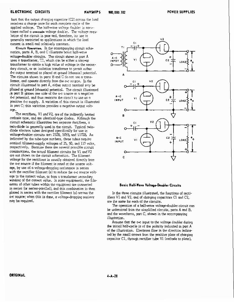
ELECTRONIC ClRWITS NAVWIPS POWER SUPPLIES
fact that the output charging copacitn (C2) across the lmd receives o charge once for each complete cycle of the applied voltage. The half-wove voltage doubler is sorw times called a cascadm voltaae doubler. The voltoe reau- lation of the circuit i s pwr and, therefore, its use is seneraliy restricted to applications in which the iwd . ~
current i s small and relatively constant. Cllsuti Operetien. In the acmmpnying circuit sche-
matics, pvts A, 8, and C ii~ustrate basic half-wove wltagedoubler circuits. The circuit shown in pan A uses a tnsformer , T1, which can be either o stepup transformer to obtain a high value of voltage in the secon- dary circuit, or on isolation transformer to permit elther d c outpiit terminal to placed at ground (chassis) potential. ' h e circuits shown in p t s Band C do not .Ise a Irons- former, and operate directly from the a< source. in the circuit illustrated in pmt A, either output terminal nay he placed at g m d (chassis) patmtial. 'The circuit illustmted k i n part B dams one side of the a c s a u c e ot o newtive d c potential, and thus restricts the circuit t o use a s o Positive d c supply. A variation of this circuit i s illustrated in p r t C; this "miation provides a negative output volt- age.
' h e rectifiers, V1 and V2, ore of the indirectly heated cathode tyw, and are identical-type diodes. Although the circuit schematic illustrates two s e w a t e iectifiers, a twin-diode i s generally used in the circuit. Typical twin- diode electron tubes d e s i ~ e d s p i f i c a l l y for use in voltagedoubler circuits are: 2576, W6, and 115% As indicated hy the tube-type numbers, these tubes require nominal filament-supply voltages of 25, 50, ond 117 volts, respectively. Bemuse there are several possible circuit combinations, the actual filament circuits for V l and V2 ore not shown on the circuit schematics. The filament voltage for the rectifiers is usually obtained directly from the a c source if the filament is rated at the source volt- age, by use of a voltagedropping resistance in series with the rectifier filament (s) to reduce the a< source volt- age to the correct value, or from a trmsformer semndory winding of L$e correct value. In some equipments, the fila- ments of other tubes within the equipment me connected in series (cx series-prollel), and this combination is then placed in series with the rectifier filament (s) a n o s s the 0.c source; when thls i s done, a voltage&opping resistor m q be required.
INPUT A - c o vlq ,I
Boric Half-Wave VoltapsDoubler Circmitr
in the three circuits illustrated, the functions of recti- ifiers V1 and V2, and of charging capacitors C1 and C2, ore the same for each of the circuits.
The operation of a hdf-wave voltagedoubler circuit can be understood from the simplified circuits, p r t s A and B, and the waveforms, pu t C, shown in the accompmying illustration.
Assume that the a c input to the voltage doubler during the initial half-cycle i s of the polarity indicated in p t A of the illustration. Electrons flow in the direction indica- ted by the small arrows from the positive plate of charging capocitor C1, through rectifier tube V1 (cathode to plate),
ORIGINAL
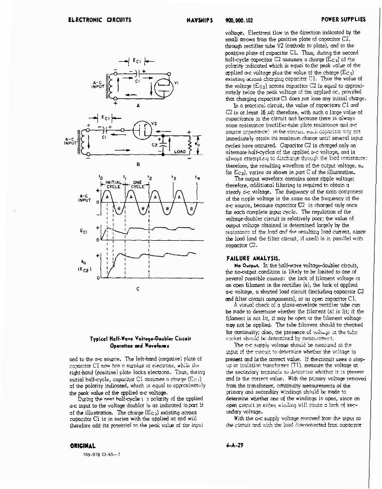
ELECTRONIC CIRCUITS NAVWIPS
m v 2
4-c INPUT 1 Q*wflilT - Co
- LOAD 1 - -
Typical Half-Wove Voltage-Doubler Circuit Operotion a d Wavebmr
and to the o~ source. The lefthand (negative) plcte of capcitor C1 now has a surolus of elecuons. h i k ihr riqhthmd (positive) plote lacks elecuons. Thus, durinq initial half-cycle, capacitor C1 assumes o charge (Ec I )
of the polarity indicated, which :s equc! to apporimate!y the p e d value of the applied a-c voltage.
9 ~ 5 : the n v t h a l f q c l e t : polarity of the applied a s input to the voltoge doubler is a s indicated in p i t t) of theillustrmion. ?he charge (Eel) existing ocross ca&citor C l i s in series with the applied oc and wiii A-- c-- -AA it- mta t io i tn the w k vaziie oi :he inpd: u>c.e,-= "",. ..- r-.-..-
POWER SUPPLIES I voltage. Electrons flaw in the direction indicated by the small mows from the positive plate of copocitor C2. throuqh rectifier tube V2 (cathode to plate), and to the positive plote of copocitor C1. Thus, during the second halfiycle capacitor C2 assumes o charge (Ecz) of the polor~ty indicated which is equal tothe peak v a l e of the &lied c-c voltage plus the value of the charge (Eel) exisillls A"--'-" "",,,,",*,,, ,,, ,,.,.,..., Cl. Thris the value of the voltage (Ecz). across mpocitor C2 i s e p u ~ l to qproxi- mately twice the peak vo!:age of the applied ac, prov~ded that charging capacitorC1 does not lose any initiol chmge.
in a practical circuit, the value of capacitors C1 and C2 i s at least 16 pf; therefore, with such a large value of capacitance in the circuit and because tiiere is alwoys some resistance (rectifier-tube plate resistance and a% s m c e i~p?donce) In the c i r ~ v ~ ~ . C U ~ I i ~ p i i j : ~ ~ ~lz; 22:
immediately attain i ts maximum chmge until several input I cycles have occurred. Capocitar CZ Is chmged only on alternate h d f c y d e s of the applied o-c voltage, and is aiways attemptirig to disihmge th~ou~!! !t:e Iood resistance: ihereiore, the resulting wavefor- o! the output voltoge, e, (01 Ecz), varies as shown in part C of the illustration.
The output waveform contains same ripple voltoge; therefore, additimal filtering i s required to obtain a steady d c voltage. The frequency of the main component of the riooie voltcoe is the same os the heuuencv of the . . a c source, becaui capacitor C2 is charged only once fa each complete inplt cycle. The regulation of the voltagedoubler circuit i s relatively poor; the value of output voltage obtained i s determined largely by the :s;ia:;~c- of the !sad nnd ?he resulting lood current, since tire imd (and the !ilter circuit, i! used! is in parallel with capcitor C2.
FAILURE ANALYSIS. No Ovtpuk In the half-wave voltagedoubler circuit,
the nwutp l t condition is likely to be limited to one of several possible causes: the lock of filoment voltoge oi an open filament in the rectifier (s), the lack of applied a s voltoge, a shorted lwd circuit (including c a p c ~ t w C2 a d hirer clrculc zm;r.nm~s:. J: I: 2;r. =;~C!OI C1.
".$a! c r x < :i 2 ;I-xs+nvelnpe rer!:!!?r !'~k can be r ace tc dr:er- :nc. ~i .nhcr :!.t !:!zrer: a ' :r ::!: !! the filament is not lit, it may be open or the filoment voltoge may not be opplied. The tube filament shwld be checked far continuity; aiso, t ie presence of vokuje a: the %be
si,oill,j k detc--'- ..iiiiirieu .' L.. ", me o.,,ra...i: ..
The a c supply voltage shouid he measured ct tL.e k p ~ t c! !he rircui! to determine whether the voitaqe is present md isthe correct value. ii thecircuit uses o s t e p Lk a is~!~:ion !rcnsformei iT11. measure the voltaqe ot the sec0nda.y :ernicinais to deter~ine whether i! :s presen! and is the coriert value. With the primary voltoqe removed from the transformei, c6ntinuity measurements of the primary and secondary windings should be made to 1 determine whether one of the windings is open, since on
. . . , . open clrcut in eirmr wiii&rLq -i!! c x s - 2 hck cf SF-
ondmv voltaae. With the a c supply v o l t a ~ removed frm the input to
.L- -:--..:. ""A ,.,:.3" ,b ,?,.,A r.lc LYLYll ...... .... diaonnected fron coacitor
ORIGINAL 4 4 - 2 9 1
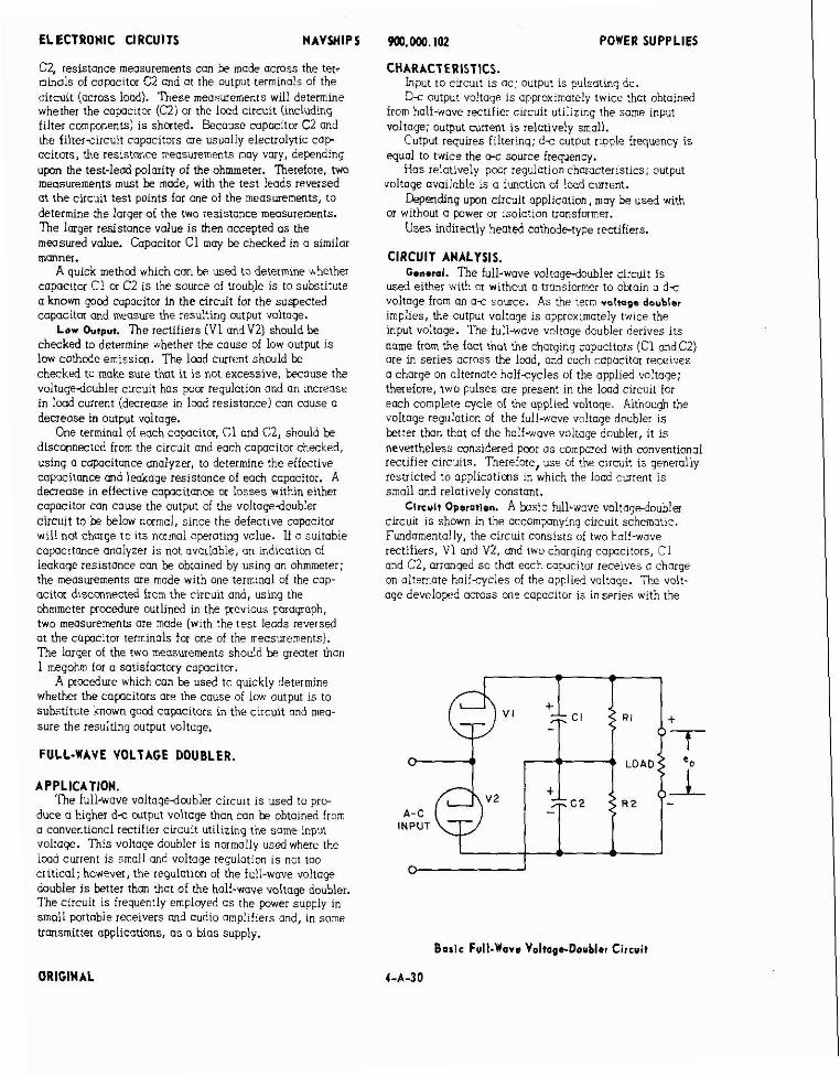
ELECTRONIC CIRCUITS NAVWIPS
C2, resistance measurements can be made across the tet- minals of capcitor C2 and at the output terminals of the cirmit (across loud). Tnese measurements will determine whether the capcl toi (C2) or the lmd cncuit (including filter comwnents) i s shorted. Because capacitor C2 and the filteriircuit capacitors are usuolly elictrolytic cap- acitors, the resistance measurements moy vary, depending upon h e test-lead polarity oi the ohmmeter. Rerefore, two meosurements must be mode, with the test leads reversed a t the circuit test points for one of the measurements, to determine the larger of the two resistance meosurements. The larger resistance value i s then accepted a s the measured value. Capacitor C1 may be checked in a similar mmner.
A quick methcd which can be used to determine hhethn capacitor Cl or C2 i s the source of uouble is to substitute a known good copacitor in the circuit for the suspected capacitor and measuse the resulting output voltoge.
L o r Output. The rectifiers (V1 andV2) should be checked to determine whether the cause of low output is low cothode emission. The lmd current should be checked to make sure that it i s not excessive, k a u s e the voltogedoubler circuit has poor regulation and an increase in lwd current (decrease in lmd resistance) can cause a decrease in output voltage.
One terminal of each capocitm, C1 and C2, should be disconnected from the circuit and eoch capacitor checked, usina a cawcitonce analvzer, to determine the effective . ~
capacitance and le&oge;esistance of each copocitor. A decrease in effective capcitance ca losses within either capacitor can cause the output of the voltogedoubler circuit to be below normal, since the defective capcitor will not charge to its normol aperatlng value. If a suitable capcitance analyzer i s not available, an hdication oi leakage resistance can be obtained by using an ohmmeter; the measurements are made with one terminal of the cap- acitor discmnected from the circuit and, using the ohmmeter procedure outlined in the pevious paragiaph, two meosurements ore made (wlth the test leads reversed a t the capacitor terminals for one of the meosurements). The lorger of the two measurements should be greater thon 1 megoh for o satisfactory capacitor.
A prmedure which can be used to quickly determine whether the capacitors are the cause of low output is to substitute known g o d capacitors in the circuit ond mea- sure the resulting output voltoge.
FULL-WAVE VOLTAGE DOUBLER.
APPLICATION. The iullwave voltagedoubler circuit i s used to p r o
duce a higher d c output voltage thon can te obtained from a conventional rectifier circuit utilizing the same input voltage. This voltage doubler is normally used where the lmd current is srrall and voltage regulation i s not too critical: however, the regulation of the full-wave voltage doubler i s better than that of the half-wove voltage doubler. The circuit is frequently employed a s the power supply in small portoble receivers ond audio amplifiers and, in some trmsmitter applications, a s o bias supply.
900.000.102 POWER SUPPLIES
CHARACTERISTICS. hput to clrcult is oc: output is pulsating dc. Dx output voltage is approximately twice that obtained
irom half-wave rectifier c~rcuit utilizing the same input voltage; output current i s ~elatively small.
Cutput requires filtering; d-c output rlpple frequency i s equal to twice the o-c source frequency.
Has relatively pmr regulation characteristics; output voltoqe ovailnhle is a function of lwd current.
Depending upon circuit application, may be used with or without a pawer or isoiatlon tronsiaraer.
Uses indirectly heated cathode-type rectifiers.
CIRCUIT ANALYSIS. G.o.ral. ?he full-wave voltoge-doubler circuit i s
used eiher with or without a tronsfoimei to obtain o d~ voltoge from an a-c source. AS the term vol+apa double. implies, the output voltage is approx~motely twlce the input voltoge. The fullivave voltoge doubler derives its name from the fact that the charging capacitors (C1 andC2) are in series across the lmd, and eoch capacitor receives a charae on alternate halfcvcles of the aoolied voltaae: . . - . therefore, two pulses are present in the lwd circuit for each complete cycle of the applied voltoge. Although the voltage regulation of the full-wave voltage doubler is better than that of the half-wave voltoge doubler, it is nevertheless considered pwr os compared with conventional rectifier circuits. Thereiore, use of the circuit is generally restricted to applications in which the load current is small and relatively constant.
Cl~cult Oparmtlen. A h s i c full-wave voltage-doubler circuit is shown in the accompmying circuit schemot~c. Fundamentally, the circuit consists of two half-wove rectifiers, V1 and V2, and two charging capcitors, Cl and C2, arranged so that each cauucitor receives a charge on alterrate haifcycles of the applied voltage. The volt- age developed across one capacitor is inseries with the
0-
A-C INPUT
ORIGINAL
Basic Full-Wore Voltage-Doubler Circuit
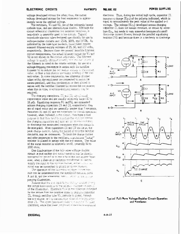
ELECTRONIC URCUlTS NAVYIIPS
voltage developed onoss the other: thus, the outout voltage develowd across the !oac resistance is r p p a x - imately twice the applied voltage.
The rectifiers, Vl and V2, ore of the indirectly heated cathode ty-, end ore identical-type d d t s . Although the circuit schematic iiiusmntes ! A D SCXTOIC recx:i?r\:, 0 twm4lode is qeneioiiy use4 in !::e cncut . Typcsi k in41ode eiecirnn t~ikenrj?siqn& suecilicoiil fcii uji in voltoqedoublei circuits are: ijZ6, W 6 , md ii7Z6. As indlcatd by the tube-tyw niiii:kr;. :rasse twez :?wire nominal filament-supply voltages of 25, 50, and 117 volts, respectively. Because there or? sever01 pss ibie !~!czent circuit combinations, the :c?da: filmlea! c ~ r m i : fai ' i ! a;? 'v'2 is no! shown on the iircu;: ;c5rcat:c. ' h e i i !c~er t
! .--- ;" ,-.,-I,. .k ,-.-.- i - ..--. , .~.. ?.;: ", . f ." ..-y- ." ~ .~ . , the filament is rated at the sowce voltage. ~y use or 0
witoge-impptnq resistonce in series wiiir d m r ircilti.i Iiiammt i s ) to ieauce ihe ;r: -c;;,c ;u.::+ .- _I.= :;:.;;: -- '.-- - .."..":-."-. -..,.-,.,in,,. *In,iin? , , i ,he C07. " ,,,,., ~,. .." .,,- ,,-"~",, ,. rect value. In some emipnents, tne iiiomenis c i ctnrr t u k s within die eq~ipment are co~.nected in spiies (m series.paralle:), md c u r r ---b- .,,a ..-.. . .- .- +:-- .:-..A ,.---- ,n ... series wlth the rectifier filament (s i across <he i€ sowce; when this is don% c vciro~e?lroi,i-,j irs:s!'>; 0) k i required. .. -, Tne cnorlj~ng c ~ a c i t o i s . 3: u , ~ - L , ;c ;: i;-,>i capocitmce volue md ore usuzliy ieiotivrly i aue i 13 to 16 pf). Equalizing resistors R1 md92, ore com2cted across chorying capmitors 2 1 md 2, respecllvt!y; hey me of equal value md ore qmerolly (iratei than ? meqohms, iieslstors K! nnd !32 m e not ? w e i s n v ;r:! r-irctrli oarlmil; , . however. when include3 rn t l - c:n,;:t. :bey hove o dun1
:- .L-. .L-.. *""A .. ,,-, .!,~,.. .*<, ,-,,...m- qn7ne,c ,"li,'-iC L 1 1 I,,Y. ..,=. . . . . . .
. . the ;:,a.ljing 23p-;Lt-ri ;:; 3 : ~ x: 37 .,I:"..,.. . .:, .hr.- . , ,
to discholge the ossoclatea copacliors wnen ine c l r c u i ~ ~s de-energized. tinen capacitors 21 ond 2 art. i m j s , 'u:e gsak c t x q e z ~ r ~ x : : 2 ~ ~ : ; ::.z ;c:iz? :! :.7.2 !k.e recti!ie: conducts, may be excessive. 70 limit the charge ccrre.li
and niter prorecuon to the rectifiers, u I ) I L . ~ ~ L L ~ Y C ''pyi16''
resistor i s placed in series with the o-c source. i?le voiue o! the surge resistor is ieiotivel~ srnnll. generally 55 ta !DO? ehmg.
one :,sadvai>~ooe -' ", .re L , i::!i- ::-:.e .!c!t3n-?Lch!er circuit 1s thgt neltnei d-c ouip,.: ieminni con be il:wlii n?.r!e?.?l !" ,rrr,iv- .r t n nn- ? > I ? Q! the 7-C s04ri'F. i n # - eve:. :ube:. :: :!e3-:~ .! iw!ztn.p ! r ~ n c f ? r m ~ r i~ . $ ? ? f; - * " " t " , , , , 1,,, , .. ~. ~ ~ . . . -;., , . . ., . . . ...l,.z! may Se connrc!ec !3 k?rli: j r r j i;:
?,p 3perL"li3c ni !?? 1,2,:-.v=,,; ""r"i-o- . ,..,, +( .+:- ~a
cuit can k understood iroa !ye ~imol;l;c?c!rr~::s, y r r s A -.A ir y n i n c wnietnr-s 711: , .--: .. .: .: ; . : . !- . . - . . - . pcying il!ustrc!io?.
" , : , ; : , : : ~:.~:~.:- .. . , - . ihe ,niriai "oii-cycir ? > 21 ;.- J;.,>T,i. , . :~:::e. , ,-, ;;::: ... ;f the i!lustr2!icr. C 'p rnc r 'I-... 'n t . 3 I,.*-:t.r : - : ,^? t~i hu thy mrnris irom T ~ P ?cslt:ve ~in!e L L ;?.2:.1i:. :aoa:lt~7i -. -,, th:Ougi, r2ciij:- ;"L "' ..-A- .- - ,-.-, ... " ,,,, ,-r '.EC " L ;zm.!:<*r .. <.A,.=, , L l > d l ~ , b ,
ine 3-c sau:ce, qr;.;. !> ~ ! > e ( W ~ J ? , ~ ~ - ,L IZ r.: T:;::,:,~ ::;= . . ( 1 : . , . : , . - - . . _ . , .. J , . , . , a
n!nC?.lE, .""!* !?? !"we' . ?* ! l r l . ,n . n i l , + r.,, :, s,,,~,;", ~i
WO.WO.102 POWER SUPPLIES
electrons. Thus, during the initial hall cycle, capacitor Cl
v::!:qe. n.e ,?lt>ce ( Z y l J 3eve!=pe.: 3x05s chcrqlnq .~3 : . t z : .'. 32,:s 231 ten a- 7nlJliOi. 7; slrnr :r, n x w -
... t'-,, C.L :e& 1) .ICI) ~:men*:! bec?;seol? snall :..,:' .:4- ?'.';?.! :!'..%.r; C-.:::;:. !".e >:tl..t?l ? ~ . 0 1 1 ~ . ' > 4
r:;.j::: ' .. r: >?::;?* z 2:: .: : l""??,~ !? ::sc,,r,e
A-C LOAD INPCT
. . , , - .
. I --r---- ac iflcz ZHARSE
. . C l CHARGE --
Ty;:::! F~.l!-%rt Vo!tagcDwbler Circuit Operotion .ad Wavdomr

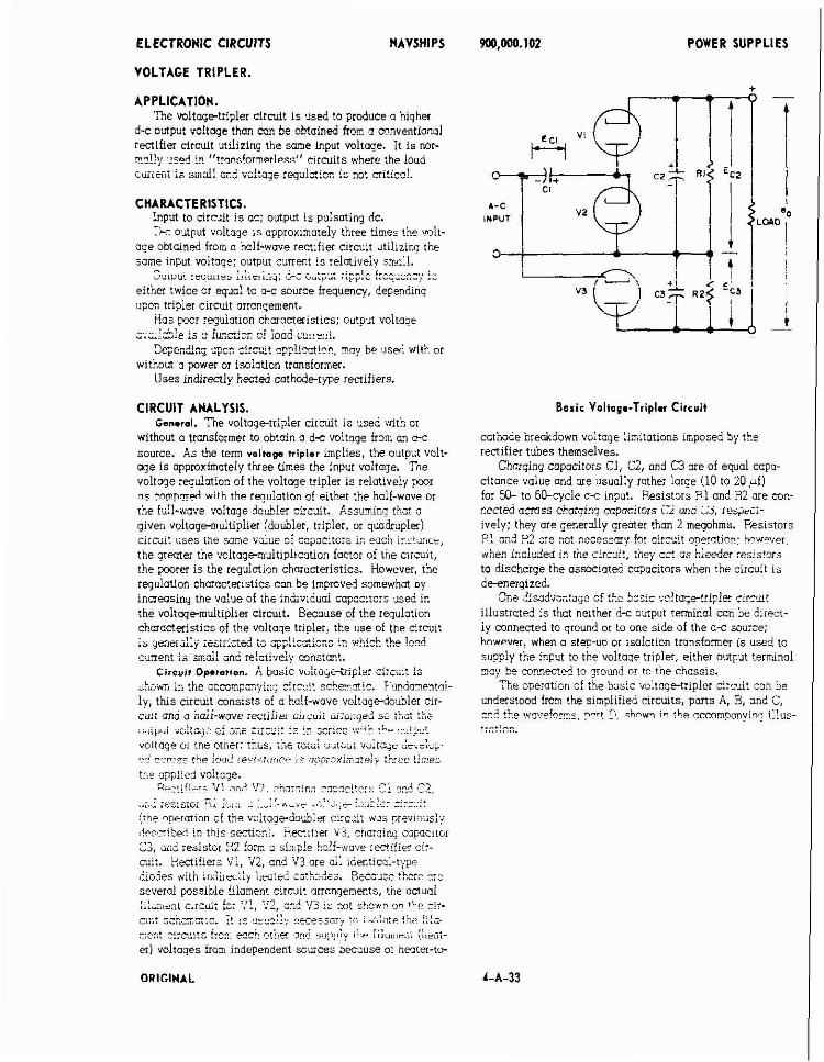
ELECTRONIC CIRCUITS POWER SUPPLIES
VOLTAGE TRIPLER.
APPLICATION. 'Re wltagetripler circuit i s used to produce a higher
d-c ou tp~ t vo!tqe than con be obtain& f19m n nnventionol rml f i e r circult utilizinc the same input voltage. It i s nor- m?!!:, nse? in "tmnr!nmsrl~ns" circuits where the load mirent i s smdl and vohage r~guimicn i s not critics!.
CHARACTERISTICS. Input to circuit is ac; output is pulsating dc. Crc output voltage i s opproximotely three times the volt-
age obtained from a half-wave rectifier circuit utilizing the same input voltaqe: output current i s relalively small. -
vuruu: : e u u i ~ = ; LLlic:ivq; i-c L:;.;: ;ic-,!c kc;-:nc,; i: either twice or equal to a-c source frequency, depending u3on trioier cucuit arranaement.
Has p a r regulation cnarocteiistics; output voltage i-i:- ;. .. :.."".;-. "; :""A ,..,..-.,;
".".Ld".C .a d .",,L.A",. 2. .""* ." .. b,...
3e;enan~ zpcn circuit cpp!ico~!n?, may he lrsd with or without a power or isolation transformer.
Uses indirectly heated cathoderype renifiers.
CIRCUIT ANALYSIS. tsn.roi. The voltage-tripler cirmit is used with or
without a transformer to obtain a d s voltage itom an o s source. As the term voitaos h ider im~l ies . the outnut volt- - . . . age i s approximately three times the input voltage. 'The voltaqe rwulmion of the voltaqe tripler i s relativeiv poor . . . . . ~
cr cnmpmrvi with the rqulotion of either the holf-wave or -L L.11. .-ye .. I+..- in.,hlnr rirr>,it ~c):m;nn fb,-+ - e u . " . O A . " ~ ~ "" -.-. A . "l u
given voltagemultiplier (doubler, t r i~ler , or quadrupler) circdit uses me =me vsue ci Ca?aCitors ii: s c l ! ~RL:u~IC-_ ,
the greoter the ~roitagemuitlpi~cotion factor oi the aiclrit, the poorer i s the regulation characteristics. However, the regulation characteristics con be Improved somewhat by
, . inamsing the value of the in&vidiiai capomtors usea :n the voltagemultiplier circuit. Because of the regulation characteristics of the voltage tripler, the use of the nrclllt ib ,,ec,erully res::iesd :c ap;!icaticns in *..!h!ch the !x? surrer.; is smd! and re!ativeiy mnstmt.
Circuit Dpetotjon. A bosic voltagetriplei 6;iji: is , i n : ,e U L L U ~ P U ~ --- ---..:-- .,..,, - "11 -..- u,... ..-hemmic. >-.. , ?llndaFental. ly , this circuit consists of a half-wave voltagedoubler a r - . . cul: and a nmr-wove rff~iiirr Ciicuii diljiiije6 si i:zt :hi ,,.,ipzi -' --- .- :.. - .:"" .... ;L +I., ... :<..,: . L G, , , . . . . . . voitnqe oi tne ornsr: thus, r e ;KG~ Y Y ; ; Y ; :a:~;~= :C..i!ir.
r+ r r n c i ti.. i n 4 iecictavci : s ~ ~ a z i ~ ~ i , x a r e ~ ; ::-JCC the:
~. . -. . ",,- ,ec, -.?. - .. . . .>.. ,.LZ !. -.".". . .. .. :.2!--.., .,.;..A- ., ,... ;.. j t h ~ memion oi the voiroaedoubier clrcoit ws ni?vircsly :+?$.-!be3 in this section!. %t:!ler i r3, cnorolny capaciror Cj, md resistcr 22 form a si-pie hzli-;uo.:s reeifier cir-
I > . I I I rC!+ - r c z % - I RIZ 1 =CZ I I I I I I
INPUT A-c 1 v2 a 1 I 1 fLm<
Boric Voltape-Tripler Circuit
cathode breakdown voitoqe lizitations imposed by the rectifier tubes themselves.
Charging capacitors C1, C2, and C3 are of equal copa- citonce value and me usually rather large (10 to 20 pf) for 50- to 6bcycle a s input. Resistors R1 and R2 are COP
cected o m s s charqinq copacirors i i uno i3, resprii- ively; they are generdly greater than 2 megohms. Res~stors 0 1 - - A D1 -- --. --r-rrm.. h r rirrt!it nnernt inn hnwpyer, ,.. ".." . ,d. -.= ,..,. ,.-buudd, .". witen ir.cluded ic the circtiit, thcy ac: os bleeder res:sr~is to discharge the associated capacitors when the circuit is de-energ~zed.
gne *sa&--."" , + L"C<+ .m u ,..,, e ... ... c wu... . .!!age!ri:ler cicui! illustrated i s t h n neither d-c outpur terminal con be direct- ly connected to ground or to one side of the a s source; however, when o stev-up or isolation transformer i s used to supply the input to the voltaqe tripler, either output terminal zsy b mnnecte? to qmund or to the chassis.
The oneration of the bosic voitagetripler c i ro~i t csr. be understood from the slmpliiied c~rcuits, pans A, 3, and C, 2-4 !hs %C'!D!C.?-S . -^rt = - ~ ~ " ~, chnwn i n t6e ncmrnponvinn illus-
..".8".. , , , , , , , , , , .
-.<. ,,,.. Rectifiers V i , '42, ond V3 ore ali identical-type diodes with iilGiinily lioitrl iii5;dis. D=cuzc thcr2 1 : ~
severd possible filament circuir arrangements, tne actual :;:a,,sn: ;;ic&; ic: '.'I, :'?, -:? ?'3 i- 301 sbcnn 9. the ,-ii- - .... :. ,- ,-,, .::,, .uwii;ii :; isn:o:i !L; : jLa- ,.,... .>- ..-.., "~.-. .. ." ----.., ....... ~ - , . . ---. ,..L,,. -..-..'" k..b".." '.-- .. -.. ..".. ""A s,?:,,>:" ,!." :i: ,,,,,,; (:,ijt- ,. , er) voltages born independent sources Dec3use of cecter-tv
ORIGINAL
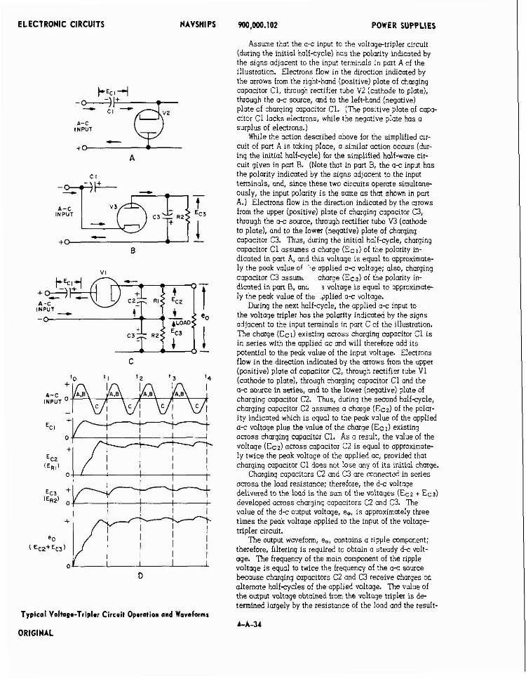
ELECTRONIC CIRCUITS
A -C INPUT
A-c INPUT
EC I
E ~ 2
Typical Voltap*-Triple, Cirrmit Operation and Wovefwms
ORIGINAL
W O , ~ . l O 2 POWER SUPPLIES
Assume that the a-c input to the voltagetripler circuit (during the initial hdfsycle) has the polarity indicated by the signs adjacent to the inpu! terminals in part A of the illustration. Electrons flow in the direction indicated by the arrows from the right-hand (positive) plate of charging capacitor Cl, though rectifier tube V2 (cathode to plate), through the c-c source, and to the left-hand (negative) plate of charging capacitor C1. (The positive plate of capa- citor Cl lacks el&rons, while the negative plate has o surplus of electrons.)
While the action described above for the simplified cir- cuit of pan A is taking place, a similar action occurs (dur- ing the initial half-cycle) for the simplified half-wwe cir- cuit given in part B. (Note that in part B, the a-c input has the polarity indicated by the signs odjocent to the input terminals, and, since these two circuits operate simultane- ously, the input polarity i s the sane a s thai s h e w in part A.) Electrons flow in the direction indicated by the arrows from the upper (positive) plate of charging capacitor W, through the a-c source, through rectifier tube V3 (cathode to plate), and to the lower (neqative) plate of charging copacitor C3. Thus, during the initial half-cycle, charging capacitor C1 assumes a charge (Eel) of the polarity in- dicated in part A, and this voltage is equal to approximate- ly the peak value of ',e applied a s voltage; also, charging capacitor C3 ossumr charge ( E c ~ ) of the polarity in- dicated in pan B, ank ; voltage i s equo! to approximate- ly the pe& value of the pplied a-c voltage.
During the next holf-cycle, the applied o-c input to the voltage tripler has the polatlty indicated by the signs a d j a c ~ l t to the input terminals in part C of the illustration. The chaqe (Ec i ) existing across charqinq capacitor C1 i s in series with the applied ac md will therefore odd its potential to the peak value of the input voltage. Electrons flow in the direction indicated by the atrows from the upper (positive) plate of capacitor C2, through rectifier tube Vl (cathode to plate), though charging capacitor C1 and the a s source in series, and to the lower (negative) plate of charging capacitor C2. Thus, during the second halfcycle, charging copacitor C2 assumes a charge (Ecz) of the polar- ity indicated which i s equal to the peak value of the applied a s voltage plus the value of the charge (Eel) existing across charging capacitor Cl. As a result, the volue of the voltage (Ecz) ocross capacitor C2 i s equal to approximate- ly twice the pmk voltage of the applied ac, provided that charging capacitor C! does not lose any of i ts initial charge.
Charging capacitors CZ md C3 are connected in series ocross the load resistance; therefore, the d-c voltage delivered to the load i s the sum of the voltages (Ec2 + E c ~ ) developed ocross charging capacitors C2 and C3. The volue of the d s output voltage, eo, i s approximately three times the peak voltage applied to the input of the voltage- tripler circuit.
The output waveform, e,, contains o ripple component; therefore, filtering i s required to obtain a steady d s volt- we. The frequency of the main component of the ripple voltage i s equal to twice the frequency of the a-c sauce because charging capacitors C2 and C3 receive charges on alternate half-cycles of the applied voltage. The value of the output voltage obtained from the voltage triplet i s de- termined imgely by the resistance of the load and the result-
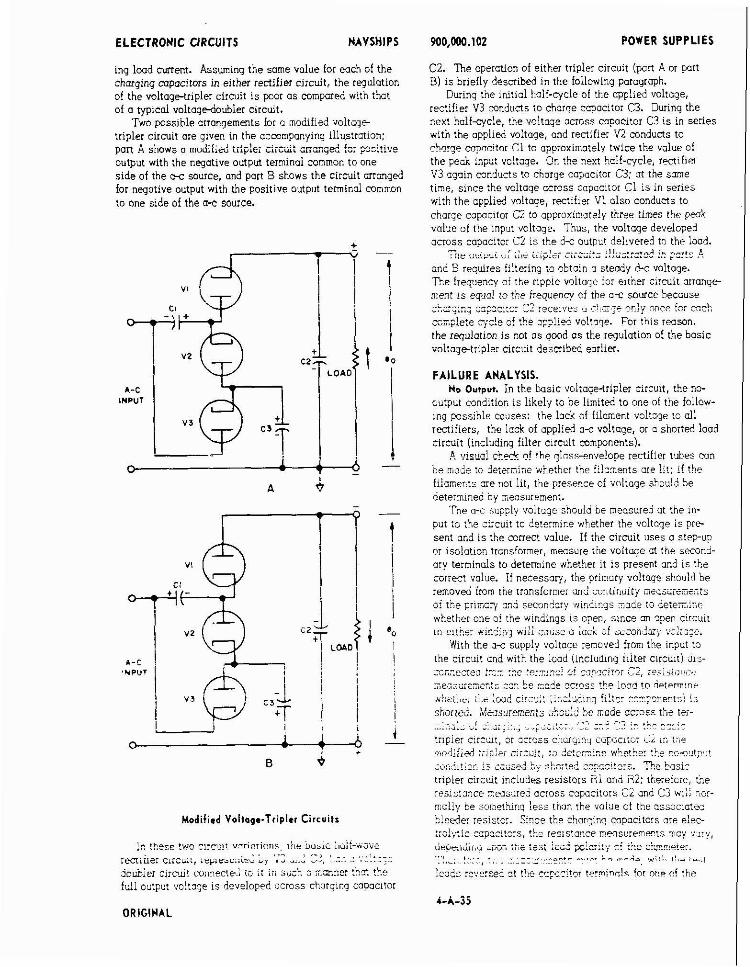
ELECTRONIC CIRCUITS NAVSHIPS
ing load current. Assuming the same value for each of the charging capacitors in either rectifier circuit, the regulation of the voltage-tripler circuit i s poor a s compared with that of a typical voltagedoubler circuit.
Two possible arrangements for a modified voltoqe tripler circuit are given in the accompanying illqs!rmion: part A shows o rnuhfid iiiplei iirc-: ai;;ng.d for ?zi!iue output with :he negative output terminal common to one side of the o-c source, and part B shows the circuit arrmged for negative output with the positive output terminal common to one side of the a-c source.
Modified Voltop.-Trip1.r Circuits
I. tL.-.,. twn ">,",,l! "l!iorinns ti,r "">LC i,":i-.j;e .., "- ... " . . . ..^ ,,., , . ~ .... ? ,-.. ieniuei clrcd:, ;rpisac;iic.. r r 4,.u -,, .. ;.
jo*jer clrc,ii vu,,nriie~ , # '- $u .' L L :- t#8aub,, --.-L u ,..- ..... +Lnt ..,-. tho
full o-tput vo!ts:e is developed Dcross chorglng copocitor
900.M10.102 POWER SUPPLIES
C2. The operation of eitt-er tripler circuit (part A or part B) i s briefly described in the following paragraph.
During the initicl ha]!-cycle of the applied voltage, rsctifier V3 mnducts to charge capacitor C3. During the next half-cycle, the voltage ocross capacitor C3 i s in series with the opplied voltage, and rectifier VZ canduns to rhnrne rlnpncitot Cl to opproximatel~ twice the value of .L- La ,= rEuk --- inpu: voltoge. On the next holf-cycles r ~ c t ~ f i e ~ V3 again conducts to chmge capacitor C3; at the some time, since the voltoge across copocitor il i s in series with the opplid voltage, rectiiier V1 also conducts to chorqe copac1:ar C2 to approximately three times the peok value of the lnput voltage. Thus, the voltage developed across capacitor C2 i s the d-c output delivered ta the loo-?. -
::lr U S L ~ ; v: ;iSr c;;:;~:z ~ ! ! Z Z : : C C ~ i-. n and B requires filtering to obtain 3 steady d-c voltage. P.e frequenq of the rlpple voitoqe ior elther mrcuit arrange rne.nt !s equnl to the frequency of the a< source because
, , - , , , .I ---- - - I . . ".*" '-. "",.!. -,,.,, y.,,v "" ?*-,. ". -- ,-.-,,.- 2 , , . JL ,>T,~ , , l , y \ , , , , - ,~,, L..L.,
xz;!e!e ?;c!e c! the qpl ie? voltn?e. For this rwson. the regulation i s not as goad a s the requlation of the basic voltogetripler circuit desnibed wriler.
FAILURE ANALYSIS. No Output. In the basic voltage-tripler circuit, the no-
output condition i s likely to be limited to one of the follow- ing possible c a s e s : the lack of filament voltoge to all rectifiers, the lack of applied o-c voltage, or o shorted load circuit (including filter clrcuit components).
P. . i i s ~ ! r h e c h ! the ?Inns-envelope rectifier tubes con be -a& t i jeterrine .whetkc: the !i!z:.ents are lit: if the f i lorcr ts ore not lit, the presence oi voltage should be deterrnlnea by neaswemen:.
The a-c supply voltage shouic be measured at the in- - ,I,, .. . ,o :he circuit to 5eterxir.e whether the voltnge is p r e
sext and i s the correct value. If the circuit uses a stepup or isolotlon tronsiormer, mwsure the voitage at the second- ary terminals to determine whether it i s present and i s the correct value. If necessary, the primary voltage should be r e m o d itom the rronsiormer ad cu~,tii~ui[y i i l e~s~ ie rn iz :~ oi ii,e p;i;r.ar( mhsecandory w l d l r g s l ode to ?ete;;;i;.c whetb,er one of the wlndings is open, since an 3pen circuit ;:I r i t ha winin: viii c a s e s luck a! sexn2iii j ;.cl:;;i.
With the Q-C suppl.9 voltage removed from the input to the circuit and with the ioad (including iiiter circuitj As- :c:~7,c~ec :zz :zc !c:.7!y2! + ?~;>,>cir,;~ ,-2, :?s;s;c;;j(:.
ze;;;rs-c-.!: :cn be -c?E. CIC:OSE the load to ieterm~nr . " : ,~ i : ,~ , ::,= :G": c::ci: ::?,:!.;5:~: !:kc C~-,;~PZ?!?! i: shorted. Mmsuiwen:~ 5'iai;ll Sc made across the te:- .: ! . : . . . .~~ ;.-, ..> -3 ;.. .L-L-,.- . . " . . . . .... .,. . . .....
t::ple; c;:car, or across cr!wglnj c~pacitiir L.I ,il t x .i,i..:;fi& ,,rii,c: .-.:'-- i r r i r u , , .- , L , " ic* .r --.- ...,.,, C w id'-. ..b...-. .ha nn -,,fl,,,
i . ' " r :; - 2 L.. ..L^. ,."p,"",,"vc :lL:,d.. .. >,: .~ ,,,,. te? ""?" 9 . e k.asi?
tripler circuit includes resistors 3 1 and 22; thereicre, Lqe resiz:snce r.msurei cc:oss capacitors Zi and C3 w i l l -,or- ma!!y be rarnethinq Less thon the vaide 01 the ossaclote hlcde: res:stor. 'ifice the c5orqinq copocitars are elec- :;c!,,<ic c3pc::tcrs. !!.e res!stance rn%sureme?ts 30" ,,dry: . . . liepel,;,,." iwil i:,s tc;: :2c: XIc:::i' "i " s "b.?.~!'!". '.'I .,,.,,, - 8 - - . ~, ' . .. - , - -- ..--n...r .~ -,,". L"-";- ,";qL $;," ,-.I
!zc.'z :e iz:s? z! !he czpncitg~ t~r.njnn!s for OPP O! the
ORIGINAL
ELECTRONIC CIRCUITS NAVSHIPS
measurements, to determine the larger of the two resistonce measurements. ' h e laroer resistonce value i s then ac- cepted a s the measured value.
L o w Output. ?he rectifiers (Vl. V2, and V3) should be checked to determine whether the cause of low output i s low cathode emission. The llad cmrent should be checked to moke sure that it is not excessive, because the voltage- tripler circuit has paor regulation and on increase in load current [decrease in load resistance) can muse a decrease in output voltage.
One terminal of each charging capacitor (C1, C2, and C3) shduld be disconnected from the circuit and each capo- citor checked, using a capacitance analyzer, to determine i t s effective capacitance and leakage resistance. A d e crease in effective capacitance or losses within the capa- citor can couse the output of the voltoge-tripler circuit to be below notmal, since the defective cawcitor will not charge to i ts normal operating value. If a suitable copa- citance analyzer i s not available, an indication ot leakage resistance am be obtained by using an ohmmeter. First. disconnect one terminal of the capacitor from the circuit; then, using the ohmmeter proceduie outlineY for the n m - put condition, make two measurements (reverse the test leads at the cabcitor terminals for one of the measure- ments). The laroer of the two measurements should be greater than 1 m$oh for a satisfactory capacitor.
A procedure which can be used to quickly determine ~. whether the capacitors are the couse of low output i s to substitute known oood capacitors of the same value in the voltage-triplet circuit md measure the resulting output voltoge.
VOLTAGE QUADRUPLER.
APPLICATION. The voltagequadrupler circuit i s used to produce a
higher d-c output voltoge than can be obtained fmm o con- ventional rectifier circuit utilizing the some inpui voltoge. It i s normally used in "transformerless" circuits where the load current i s small and voltage regulation i s not critical.
CHARACTERISTICS. input to circuit i s ac; output i s pulsating dc. D-c output voltage i s approximately four times the volt-
age obtained from a half-wave rectifier circuit utilizing the same input voltage; output cunent is relatively small.
Output requires filtering; d-c output ripple frequency i s either equal to or twice the a-c source h-equency, depending upon quadrupler circuit mrangement.
Has poor regulation characteristics; output voltage available i s a function of load wrent.
Depending upon circuit application, may be used with or without a power or isolation transformer.
Uses indirectly heated ca!hodetype rectifiers.
CIRCUIT ANALYSIS. G.n.r.1. The v o l t o g ~ a d i u p l e r circuit i s used with
or without a transformer to obtain o d s vohage from on o-c source. As the term voltage puodrupl.r implies, the output voltoge i s opproximotely four times the input voltage. The voltage regulation of the voltoge quadrupler i s very pmr a s
WO,M)0.102 POWER SUPPLIES
compared with the regulation of either the half-wave oc the full-wave voltage doubler circuit. Assuming (hot a given voltagemultiplier (doubler, tripler, or quadrupler) circuit uses the same value of capacitors in mch instonce, the greater the voltage-multiplication factor of the circuit, the poorer will be the reaulation characteristics. Because of the wc: rcclctior crmacterlrt:cs cf Ire volrqe qu~Cr~.)Ier, the ise o! the circut i s qenerd!y resitrind lo appbcatlons in w'l~ch the lmd current 1s sad1 ml re!?tively constcnt.
CI.CUII Op.rot~on. 'Twc k s 1 c voltoqe(ll;~fupler n r - ~ ~
cuits me shown in the accompanying circuit schematic. Each circuit (part A or pmt B of the illustration) mrisists of two half-wave voltage doublers aranged so that the output of one doubler circuit i s in series with the output of the other; thus, the total output voltoge developed ocruss the lmd resistance i s approximately foln times the applied voltoqe.
Rectifiers V3 and V4 and charging capacitors Cl rmd CI form a conventional half-wave voltagedoubler circuit (the operation of the voltagedoubler circuit was previously described in this section). Rectifiers V1 and V2 and chmg- ing capacitors C2 and C3 farm a second half-wave voltage- doubler circuit; however. this voltoaedoubler circuit ooer- ales in cascade with the first volta~edoubler circuit a"d obtains i ts input from the valtwe available across the series combination of charging mpaci& C1, the applied a* input voltqe, and charging capacitor C4.
Rectifiers V1, V2, V3, and V4 are identical-type diodes with indirectly heated cathodes. Because there me several possible filament circuit arrangements, the actual fi lment circuits are not shown on the schematic. It i s necessary to isolate the rectifier filament circuits from each other be- cause of the heater-tosathode breakdown voltaae limitation imposed by the rectifier tubes themselves; therefore, a fila- ment transformer with s e w m e well-insulated secondmv windings, or a single tr&sformer for each rectifier tu&, i s required. This reauirement for an independent filament (heater) voltage source for each rectifier tube places a practical limitation on the use of electron tubes in valtase multiplier circuits; for this reason, the voltaqequadrwler circuit and other voltagemultiplier circuits generally employ semiconductor diodes a s rectifiers in Lieu of electron-tube diodes.
Charging capacitors C1, C2, C3, and 01 me of equal capacitance and are usually relatively large (10 to 20 pi) far % to 6C-qcle a s input; however, for some high-volt- aqe, low-current applications, such a s in the hiuhvoltaae supply for cathod&iay tube indicators, the chaiing m&- citars may be relatively small (0.01 to 0.1 pf), e smla l ly if the a s input frequency i s much hiqher than the "armal. S- to 60-cycle input frequency.
Resistors R1 and R2 are equalizing resistors for chmg- ing copacitors C3 and GI, respectively; they me of equal value and are generally greater than 2 megohms. Resistors R i and R? ore not necessary for circuit operation; however, when included in the circuit, they have a dud purpose- they t a d to equalize the voltages across chmqing capo- citors C3 and GI, and they also act a s bleeder resistors to discharge the capacitors when the circuit i s d-ergized.
The operation of the basic voltagquadrupler circuit can be understmd from the simplified circuits, pms A, B,
ORIGINAL
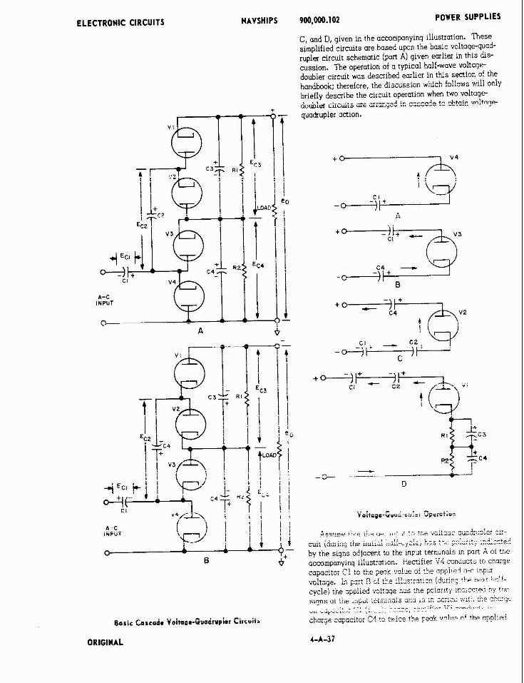
ELECTRONIC CIRCUITS 900,OM).102 POWER SUPPLIES
C, and D, given in the acmmpanyinq illustrotion. 'These simplified circuits are based upan the basic voltogewad- rupler circuit schematic (port A) given earlier in this ds- cussion. The operation of a typical half-wove voltage daubier circuit was described earlier in this section of the handbook; therefore, the discussion which follows will only briefly describe the circuit operation when two voltage do&:a cili"i;j are .; cii9^ -( iz c=Ccc*e 12 "h!lin ""If"?+-- quadrupier acilon.
, , . . + - I. ....~.--.,",,.>..,-~a. -,.- 2-q x,..~ I , . .! I , . ? ,,- . , ,. , , i , ,C "U.."UI ""I-" -.-. . ~
. . . . -.... --, .n.....,.. Xu ,;.- ... - . , . ; .,., i i.,;';;..;:;. 5;; ~~~ :+, ZC:;:::; :;?.22re6
by the siqns adjacent to the input termlnais XI port A oi the acmmpanyiw illust;otion. Eecuiier V 4 c a n i ~ c ~ s lo charge ,?i3ci:o; C! to the p n k v a l ~ e of !he applied o-c inpfi
I-. 9 sf f*e :!i.strgi!?n [?:;iil; tl;r ir,! :cl!- the ;po!ied vc!:~qe b.ci the pc!zny !nc?co!e: . , ?y , i"?
i,rbui ~ - , - ..A . - .- -a7. ". .,...- . m e "" .,.,.- .,I,,,,, u a ui,u '* .,L,A<." ...... -..-y-
. . . , ., . , ., , t- . . ,, . -""", ,-.c .. ,>,;.-up "*..", -. %... ~: . ~~~~
A__- -- -is... -n i, +,.;PO ,hi v n l ! ~ nf the n p p l i d ,,UV -" rl-.i-. - . ." - - - i - -~~
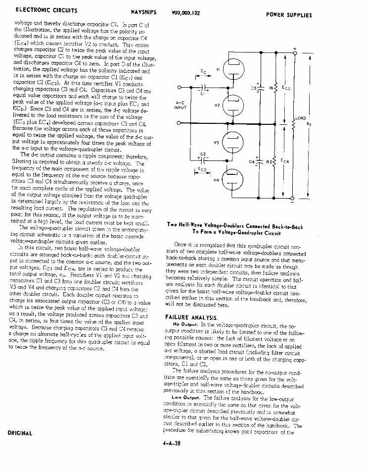
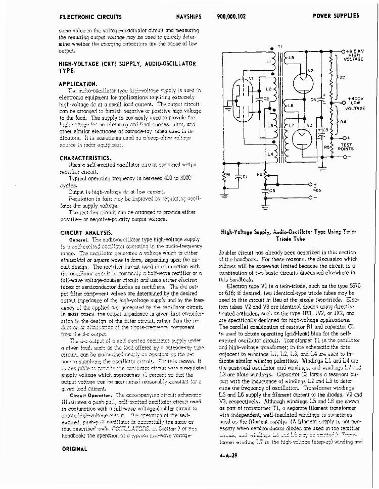
ELECTRONIC CIRCUITS NAVSHIPS
same value in the valtagequadrupler circuit and measuring the resulting output voitoge nay be used to quickly deter- mine whether the chorglny capacitors ore the muse oi low output.
HlGH.VOLTAGE (CRTi SiJPPLY, AUDIO-OSCILLATOR TYPE.
APPLICATION. -L , , , e ilu3iwsciilator type bJ;?-vcltoge sopply is used i n
electroiuc equipment far opplicmions requiring extremely high-voltoge dc at o smcll load current. The output circuit con be arranged to funis5 nqotive or positive high voltoye to the load. The supply is comnoniy used to provide the bi;h VG!!I-- 3~ f-7 ~~~ nr r~1m.rmln~ md final modes: ultor, nni other similar electrodes oi catnoderay lubes used iri irk dicutors. it is sometimes used :; c kecpalive vc!!c:e sc;;ce ir. radc: equipment.
CHARACTERISTICS. Uses o self-excited oscillator cirniit combined with o
rectifier circuit. Typical operating frequency is between 405 to 3OOO
cycles. Output i s high-voltage d i at low anen t . - ilequlotian i s foir; may be impraved bj rejulat::; uscil-
lator d-c supply volroge. Tt,e reetilier circuit can be arranged to provide either
positisIe or neqative-polarity output voltage.
CIRCUIT ANALYSIS. Genorol. The audiwscillator type high-voitoqe sup?iy
is ,: >eli-cxci:2~ O Z ~ ! : ~ : ~ : c;e:c!::; i? Lh* g>:&o-!req~??cy range. The asciilator qecermes s vcliage wh~ch is either sinusoidal or square wave in form, dependrig upon the cir- cuit desiqn. The rectiiler circuit used in conjunction with :he osciilotor circrri! is mmmcnl; ; ha!!-wcve :ectifier or 3
full-wave voita&oubler circuit and uses either eisiron tubes or semiconductor diodes a s rectifiers. The d c out- :.? !i!!er -mE"ent vol~ies ore determined bv the desired outout im~edance of the bAah-volta~e S ~ P D I Y and by the f r e v ~ . ~ . "ency ~f the app! iek< g e ~ e r g t d 3/ the osc?!!ofor circuit. Ir most cases, the output impedance is given fi:st ffinsider- ation in the design of the filter circuit, mther than the re ,..-:-- ". -''-'--.'-. -1 .'. ...- :e'.,nlE..r"" en, UUL,.",, ". c..., ..,." -. ..--.. .... ~ ~
; jiven 133d. ~ c c h os the jc.5 oiieiei j., 1 :s!S.ode-r3:~ tioe circut. con be mainioi,i& fie&-!y c; :ons:mt 2s !hs 2-c nii!:rce s~polvinc the osl!lator cirmit. For this reason. it I, .jes;i&:e :; ;:?:.i?- :"e iccl!!z!c. -:r.--.t W!" n lpnlliotpn
supoiv voltaqe which approaches :! percec! so !hd the output voitaqe can be mainran& rwsi.niib:y ioosi&:t !ir 2 given load zurren!.
Circvlt Oper.atlon. The acccmpor,ym; 7iixIt sche-atic I- - i - . . ) I --I~A.-;+,A A,,;II~,, PI,,,,,, ,,<A .i,li>iiu,ss u yu>,iji', *... -^"..-" .... ~~. In mn!unction with o full-wove voltage-doubier cucui! to obtain !5~'.-w!to.;e output. ':he ?permlon of the seii- - .~ci !~i , ~ s h - ~ . , : ! ns,-i!!;ts: :; ;sse:!:Siv !be s a ~ e qz
rjm dei.ri1w' n'lirliirl 17%YLLAT2.D S.i; 5C:: ? c! !!:s
handbook; rne operaion or o ryprco: cull-ware vi.iraqt-
ORIGINAL
WO,OOO.lOZ POWER SUPPLIES
Hipb.i'olicpc Supply, AudieOiii!!;:;; Ti.=: k- ic; T ~ i 5 - Triode Tube
doubler circuit has olreody been described in i i i s section of the handhook. For these reasons, the discussion which tallows wii! be somewhat limited because the cirmit i s a combination at two basic circuits discussed elsewhere in ttds handhook.
Electron tube V1 i s a twin-triode, such a s the type 5670 or 6J6; if desired, two identical-type triode tubes may be used in this circuit in lieu of the singie twln-triode. n e c - tron tubes V2 and V3 are identicai diodes using directly- heated cathodes, such a s the type iB3, lV2, or 1x2, and are specificdiy designed for high-voitnge appiications. The oarallel mmbinotion of resistor R1 and capadtor C l I s used to obtain operating (grid-leok) bias for the seif- ~ r c i t e d osciilotor circuit. Transformer T i :s :?e osc:iic?~! ~ n d high-voltoge transformer; in the schematic !he dcts nn!acenl 10 windings i;, Li. 2, m,3 L-i at USE:, t; :L-
dicate similar winding poimities. Windings L l a d L4 are the ousn-puu osciliotor qrid uioiings, anZ n.ii.d;i,;;$ L2 25;
L3 are plate windings. Cqopoc~tor Q iorms c remnant cir- ::it with the inductance of wir~din~s L2 ad L3 tc deter mine the frequency a! oscillation. Yrmsformer windings L5 and L6 supply the filament current to the diades, V2 ma V3. respectively. Althouqh windings L5 and L6 me shown a s pan of transfomer TI, a separate filmen! transformer with independent, well-insdated windings is sometimes used a s the filmnent supply. (A filament supply $6 not nec- eswry when xemicanductar diodes zre . US& ' '- " rerlizer
3 , ,:.. . L . , r < k " --...*. :,, Y."-*. "i. iYi, >>LC nLirw;iy., -" ... " --- - - ...-. ~
isrnrl ~ ~ ~ d i i , g L? is lh; b:;kr.:dtqe !C!S.CI:! windiv: nnli
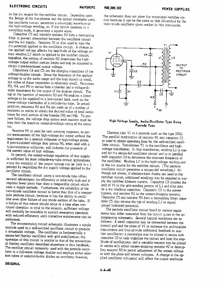
ELECTRONIC CIRCUITS NAVSHIPS
of the oscillator and will therefore affecr the high-voltage output of the supply.
FAILURE ANALYSIS 6en.r.l. The audiooscillator type high-voltage supply
consists of two basic circdts-an oscillator arrd a rectifier. It must be determined initially wherher the oscillator or the rectifier wrtion of the power-supply circuit 1s at iauir. Tests must be mode to determine whether the oscillotor 1s performing satisfoctorily: if it is, the trouble is then assum- ed to be located within the associated rectifier circuit. The failure analysis outlined in the following paragraphs i s somewhat brief because the subject of electron-tube oscil- lators i s discussed in another section of this hando&; f~cohnrmnre. the ~ r t i c u i m hiah-voltoqe rectifier c~rcuit may ~. be the same a s one of ine rectifier circuii= d r s i r ihd 2ii-
iier in this section. Since the ~ud io~~c i I l a !o r type hiqh- voltage supply i s o comhinotlon of two hosic circuits, infar- mction ancerninq !nfilir~ molysis for either Portion of rhe high-voltoqe supply can be obtained by reference to the op- plicable bosic circuit given elsewhere in this handbook.
No O ~ t p u ~ . When the oscillator is in a nonoscillating condition, negative grid voltage will not be developed across RlCl, and the measured plate (md screen) voltage of oscillator tube V1 wili be below normal. The applied filament w d plate (and screen) voltages should be mms- ured to determine whether these voltages me present and of the corren value. The oscillator tube, V1, may be re- placed with one known to be uwd to determine whether it is defective. Excessive losses in the L-C resonant circuit formed bv the transiormer and its associated copicitor wiii prevent sustained oscillation; the transformer windings should be checked for cantizuity, ofid the gcsnciated copo- citor should be checked to determine whether it 15 open or shorted. Shoned capacitor in the circuit will prevent oscil- lation; therefore, ali capacitors should be checked with a suitable capacitance analyzer :c deierzine whether they me satisfactory. An open transformer winding would nor- mally prevent sustained oscillations, however, in the twin triode osdllator circuit, there i s a mssibility that one coil could resonate with stray capacity and oscillate (at o hiqh- er !;ev~encj) and produce a !OWOIXP~J~.
If the oscillator circuit i s foun? to be functioning nor- mally, then it must be assumed that the trouble i s associated wi:h 'Le :cc::fier circsi! cr i ts !md, nn.( 1 rhwk of the t i ! i r c j t mu;: he mode !!- acsrdc?ce ,wi,i f~he pro- sedxes outlined wr1:e: in :": se*!?? !?: '. m ? ? i ! r + i ~
rectifier circuit. L o w Jutput. A re!iti.$e indixt:?: 2! ?E.c~!!c~oI "'ltplil
can be obtained by measuring the canunt oi bias voltoge ?eveloped across PIC!. A vnlne n: nlns wntrr 1s wiow normd~is an indication of low oscillotor outpur. Also, if the appl~ed plate (and sneen) voltage is t e i x :.crra!. T:
reduction in output will occw. Tne opplird fiiomeni G-L~
plate (also screen) voltages should be measured to deter- m i x ,;:hc:her !Cs; :.- vi?hjn tn!ermr-: n lapercent vmio- tion in applied fiiament voltage wili not appreciably affect the output of the supply, but o smoii change in applid plate vr.l!,m~ulp will produce 3 na~ceabie change in olnput.
5 - .-'-A- ---i"-..."'. ,,, ,,n,, hi* ," "np r r i ille ,n,rru.vus " *,,.. *". -.." -.., section (such a s iowcatnme emissi;i., iuw iiv.abi;iii.i~
900,000.102 POWER SUPPLIES
once, or an open tube element) or an open winding in trans- former T1 will cause o reduction in output. The tube may be replaced with one known to be gmd and the checks re- peated; continuity measurements of the windings of trans- former T1 con be made to determine whether any of the w~ndlngs are open. i n the pentode o~cilloto; c i ra i t , a leaky screen bypass (C2) will form a voltage divider with iiir s c r r ~ ~ ~ ~ ~ p p " ? q re;is:or (D2) an? recu!! i n = /(-PIcM(
screen voitqe: thus, ine ourpu: of ihe supply will be low. If the oscillator i s found to be operotiqg sormd!y, c
defect within the rectifier circuit or associated load must be suspected as the cause of low output. For exmple, b e cause of the relatively hlgh-impedance rectifier and filter circuits, on excessive load current can couse the output voltage to be low. Faillre analysis procedures for typical ---.' .,.... t-. .a. -'.l.i,. ..<lr -... ~. i n n:,~n-;rr,i:,7,~r ;;;cp:,cs me "u:;il:e..i . earlier in this sectior..
HiGH-VOLTAGE (CUT) SUPPLY, R-F OSCILLATOR TYPE.
APPLICATION. The r-i oscillator t w ~ hi&.-voltoae supplv i s used in .~ . . ~ . .
electronic equipment for opplimtions requinnq extremely high-voltage dc at a small load current. The output circuit can be mmnged to furnish neqa:ive or Positive high voltage to the load. The supp l~ i s commonly used to provide the . . . high voltage for the accelerating and final anodes, the ulto:. and other similar electrodes of cathode-ray tubes used in vidw indicators.
CHARACTERISTICS. Uses o self-excitd r-1 osci!lator circuit combined with
a rectifier circui!. Ty~:ca! -;pe:ct!c- !:%"el.>, is herween 4C ,>nd Wl! k;ic-
~ ~ . . . cycles.
Output i s hlqbvoltoce dc at !ow cdrren:. D e ~ ~ l n i c r , i s F o r ; m ~ y he ?mproved mns~cieroliy t ~ f
zd"tiana! circuitry to control the osc~llotor output. The rectifier circuit car. be arranged to provide either
posihve or negative-polar~ry output voiloge. Circuit moy r q u r e smel&q to prevent undesirmic
radiation from interfering with other eqliipments.
CIRCUIT ANALYSIS. G.n.r.1. The r-f osc~llator type Ngh-voltage supply 15
. . ~t beii-excitd csciihtcr z;erz:;z< 1:. ::e i w - g:!: :!,e?~.,~- liequency iurqs. Ye ;;ci:!;to: Gcc?:c!es c s:?:scilci XJT-
. . 211, W"!<.F 1s coup,e,1 <r,r"",j, 3,e ~ i ; - ~ ~ . e ":z;~*; t::..!::~:~:: to rhe high-voltage mectif;er circcli. %metimes two Irntis;i ~sai:al", :i,e> d e :::.::czd ... *".::.' ::;:::: :-- :unent outpit capooil;?j a :he 5u;p~y crri trla! diiii.iiiiiii
. . W!?. siv2ie-!,,i>e <,pe:,lG,j!,. '7% ;cz.!ic: c;:::;: 2 2 4 ::. m,nj&.;c:Lup. %:!;~; LiLe d5cL!;zr,2r ,:;?,:;;;! :z ::;2,*2>!;? 2 ?Sf- wove rectifier or o voltagedoubler o rcu t . Tne rmiiier circuit may empioy efrner electron-tubes or sen~iconducroi & d e s ns renifiers. 3: ?i. outpz! f r m the r-i oscil!ata: +igh-valtaqe sup
p!v is ;&ject to :ons:derm!e vsi:3t?m wlt5 c ci ian~r i n . . Lufc,j;, an;, t:,eiii;ri, b;;--.c o: ::- ;=L': :I.II;II,b.!l . .. . - ..- -: . i i" ^i.^..i. ir . , - ,,,, !:,, !,..,.:ir,?
~ ..--: .-. ~
ORIGINAL
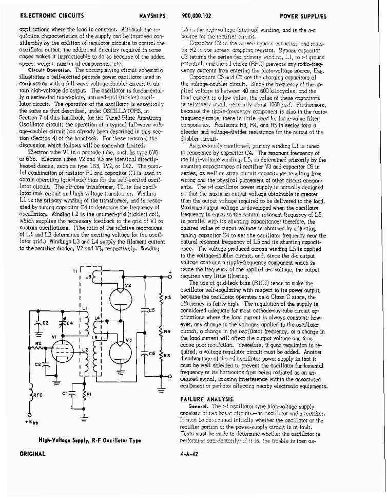
ELECTRONIC CIRCUITS NAVSHIPS
applications where the lmd i s constant Although the re- gulation chatactedstics of the supply can be improved con- siderably by the addition of regulator circuits to control the oscillator output, the additional circuitry required in same cases makes it impranimble to do so because of the added space, weight, numhr of components, etc.
Circuit 0p.rotion. ' h e ocmmDmvina circuit schematic . . . illustrates o self-excited pentode powa oscillator used in conjunction with o full-wove voltage-doubler cirolit to ob- tain high-voltage dc output. n e oscillator is fundamental- ly a series-fed tuned-plate, untunedorid (tickler) oscil- lator circuit. The o&ration of the o;cillotor i s essmtiolly the same os that described, under OSCILLATORS, in Section 7 of this handbook, for the Tuned-Plate Armstrong Oscillator circuit; the operation of o typical full-wove volt- age-doubler circuit has a l rady been described in this sec- tion (Section 4) of the handbook. For these reasons, the discussion which follows will be somewhot limited.
Electron tube V1 i s o pentode tube, such bs type 6V6 or 6Y6. Eleaion tubes V2 ond V3 are identical directly- h a t e d diodes. such a s type 183, lV2, or 1x2. The porai- lel combination of resist& R1 and capacitor C l i s used to obtain operating (qrid-leak) bias for the self-excited oscil. lator circuit. The-airsore transformer, T1, i s the oscil- lator tmk circuit and high-voltage trmsformer. Winding L1 is the primar/ winding of the transformer, and i s reson- ated by tuning capacitor C4 to determine the frequency of oscillation. Winding L2 i s the untuned-rid (tickler) coi!, wsch supplies the necessary feedback to the grid of Vi to sustain oscillations. (Tne ratio of the relotive rwnonces of L1 and L2 determines the exciting voltage for the oscil- lator grid.) Windings L3 and L4 supply the filament current to the rectifier diodes, V2 and V3, respectively. Winding
nigh.Volbge Supply, R-F O ~ r i l l ~ t o r T y p
ORIGINAL
WO.000.102 POWER SUPPLIES
L5 i s the h?:h-voita2e (ste?'~p) winding, and i s the a s source ior the remiher circuit.
Cupaci:ai 9 is tk.e screen q p o s s ccpacitor, ond resis- tor Ri 1s the scree? &oppin? resistor. Byposs capacitor C3 returns the series-fed primor" windlng, L1, to rf ground potential, and the r-f choke (RFC) prevents any radio-free uency currents from entering the plate-voltage souroe, Ebb.
Copacitcrs C5 md C6 are the charging capacitors of the voltage-doubler circuit. S~nce the frequency of the ap plied voltage is between 40 and 6W kilocycles, and the load current is a low v o l x the volue of these capacitors IS relntively srd, ?ene:zlly a5oi iWCI @+! Furthermore, because the ripple-frequer.cy component is also in the rodio- irequency range, there i s little need for large-value filter components. Resistors R3, R4, and R5 in series form a bleeder and voltage-divider resistance for the output of the doubler circuit.
As previaus!y mentioned, gnmmy winding L l is tuned to resonance by capacitor C4. The resonant frequency of the high-voltage winding, L5, i s determined primarily by the shuntinq capacitances of rectifier V3 md capacitor C6 in series, as well as stray circuit capacitance resulting from wiring and the physical placement of other circuit mmpon- ents. The r-f oscillator power supply i s normdly designed so that the maximum output voltage obtainable i s grwter fhm the output voitoge required to be delivered to the lmd. Moximum output voltoue i s develo~ed when the oscillator frequency isequal to ;he natural iesonant bequency of L5 in parallel with its shuntina mcacitance: therefore. the desired value of output vo lkge~ i s obtained by adjusting tuninq mpacitor C4 to se t the oscillator lrequenq n a r the natural remnant frequency of L5 md its shunting mpacit- once. The voltage produced across winding L5 i s applied to the voltagedoubler circuit, and, since the d s output voltage contains a ripplefrequency component which i s twice the frequency of the applied a s voltoge, the output requires very little filtering.
The use of grid-leak bias (RlC1) tends to make the oscillator self-regulating with respect to i ts power output, because the oscillotor operates a s a Closs C stage, the efficiency i s fairly high. ?he regulation of the supply i s considered adequate for most cathode-roy-tube circuit ap- plications where the load cment is always constrmt; how- ever, my chmge in the voltoges applied to the oscillator cirndt, a chmge in the oscillator frequency, or a chmge in the load current will affect the output voltage and thus cause poor rmulntion. Therefore, if gmd regulation i s re- quired, a voltoge regulator circult must be added. Another dlsadvantqe of the r-f oscillator power supply i s that it must be well shieided ti; prevent the oscillator fundomental frequency or i ts ha rmo~cs from being radiated a s on un- desired signal, musing Interference within the associated equipment or perhoos affecting newby electronic equipments.
F A I L U R E ANALYSIS. G.n-rol. I h e r-f oscillator rype hiqh-voltage supply
consists cf two basx d:cuits--an sscillator and a renifier. !t m u s t & ?ei*rm;:led initiallv whetb:er the oscillator or the rectifier partion of the power-supply circuit i s at fadt. Tests must be mode to determine whether the oscillator i s periormjng n~s!octcri!y; if it is, the troiitle i s then as-
ELECTRONIC CIRCUITS NAVSHIPS 5UO.000.102 POWER SUPPLIES
sumed to be located within the associated rectifier circuit or i t s load circuit. ?he failure analysis outlined in the following pmographs i s somewhat brief because the subject of electrontube oscillators is discussed in another sestion of this handbook: furthermore, the particular high-voltage rectifier circuit may be the same a s one of the renifier circuits described curlier in this section. Since the r-f oscillator high-voltage supply i s o combinotlon oi two basic circuits, information concerning failure analysis for either portion of the high-voltage supply can be obtained by refer- ence to the o~plicoble basic circuit alven elsewhere in this . . handbwk.
No Output. Whe~ the oscillator i s in a nonosciilatin~ condition, neqotive grid voltage will not be developed n r m s + R l C l , nnd t i e measured do te ond screen voltages oi osciilator tune Vi wlii be beiow normu:. Ths ~pp:iel filament, plate, m i screen :ro!!sges should be measured to determine whether these voltoqes are presmt ond ore af the mred ~ v ~ l u r To determine whether the ~scillator tube, V1, i s defective, it may be replaced with o tube known to be qwd.
Excessive losses ir. the airsore transformer, T i , or shorted capacitor C1. C2, C3, or C4 will prevent line oscil- lator from operating. Also, defective components in the rectifier circuit ossocioted with the hiqh-voltage winding, LS, may introduce losses into the oscillator circuit which will prevent oscillotor operation. With all voltages removed from the circuit, disconnect one lead from winding L5, or remove rectifiers V2 and V3 from their sockets: then re- apply the voltoqes and again perform tests on the oscil- lator to ?etemine whether rhr osc~ilotor *ill operme ude: no-load conditions.
I i :he ~sci!!~tar ci:cuit is !om? tc be function,n? nar- moliy, i: must be assume2 th-1 the :rouble i s ~ssociated with the rectifier circult or its load, and o check of the rectifier circllit must be made in accordonce Mth the pro- cedures outlined in this ;ectio- !or the c:p!iccb!e renifier circuit.
LOW Output. A relative indication of osci!la:or outpat cnn be ohtoined by measuring the omount of bios voltoge developed oaoss RlC1. A value of bias which i s below naxa! i s st irdicatian of !nw oscillntor output. Also, li t i e applied plme and screen voltaqes c e below normal, n reduction in output will occur. A IedKy sncen bypass cupu- cltor, C?, ,::i!! ! a ~ . 2 w!!n:e divider with screen droooing i-ristor P2 nn? r~r.;!: i - 2 iecrmse? cneen voIto7e: th l~s ; . L L . ; ~ oi!pu: ;f the i;pp!y x:!! Sc !sw. Tc deternine !+hetie: the 05c~i l~ to r tube, V i , IS [he
cnusr of lo* outpit, i: l q be replace5 w:!r o t n k kccwr !3 Se mod. Where the oscillotor circult emplovs two tilbes i;. 2 : : 3 ! ! ~ ! , 3-c ?I ?c!! f , ~ h o c mri" hp S ~ : S ? P C ~ P O 0s C O U S ~ O
l9w output. It is possible that the io* cut?;: :ori::ia: -2;. Ce
caused by 3 cilnqe in osciiiatoi trequenq away !ram tne resonant frequency of the hiqh-voltoqe windinq L5. (A e:,;~j; i- :b,: o ~ c i ! ! ~ t ~ r trnqnoncy tnwmn the ~ ~ s o n o n t freq. uencv of L5 will ordlnarliy cause a higher thor. norrncl 1.11- x t . ! A,- c?!ist-;ent of tunlnq copacltor 24 con be inode in !his r,>cr in an 3::er;F: :c 3 t t 3 1 the ? o r ~ c l ~ l i t p l i t vnltnr:e.
If the oscillotor i s found to be operating normally, a de- f e n within the rectifier circuit or the associated lwd must be suspected as the cause of low output. For example, be cause of the relatively high-impedance rectifier and filter circuits and the generally pmr regulation characteristics oi this type of supply, an excessive load rmen t can cause the output voltoge to be low. Failure analysis procedures hi tvp;ccl rectifier ci:ci!s uz& ip. biQb.-%ra!tcge sflpplieq are outiined mrlier in this section.
ORIGINAL

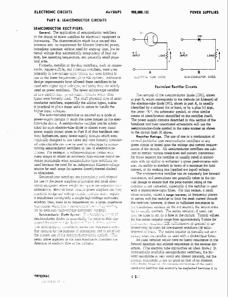
ELECTRONIC CIRCUITS f4-YSHIPS POWER SUPPLIES
PART 0. SEMICONDUCTOR CIRCUITS
SEMICONDUCTOR RECTIFIERS. t.o.ral. The application of semlconljcior reclifiers
:- ...- ,-->- -1 I<.- '-. -, .-... : -*-.: --... :. A,' " 1 5 "S""i', U' W W C , o u v p r L c ~ rui crci.uu,rir -"ur~lllo,i '2,
innwsinq. The ctiaracte:istizs wtiiih kaie caused this inlrara .~",.i.cn.ant in, i:l"-nr. I r n , . ~ . l ~ \ nrl.iar "-- ... " ...u... \-" "-, y" ..-., immedime operaiion wiihoui n R d ioi wamilp ;iae, iow in- . ,e .-- ,,,,! ,,o!:oge hop s ~ ; O s t a n ~ a i ~ e ., . -6 1 % ~ -.,
rent, low operating temperature, and rer,cra!ly small phys- i c d size.
Formerly, metallic or dry-disc rrcti!irts, such ils copper- oxide, mpper-sul!i?e, cnc r r ienim r e ~ i f ~ e r s , were ~ s e c 2*ima.i:s i ~ ) J ~ * - x : c i : ~ ~ s-.-,; :,.; ]:T.j!e3 i?
. . . . . . . v,.-.
;se :r; ;he :awe; ;;P ;:Pnr:es ;,:; ;a n;v ,-f;:e;:. ~,?,?:::onz; desijn improvements have allowed these rectifiers to be ::;ed wi!$ Lighc-r inp:: ;ol:::es; t a d q :h=; :re .n.ilc!y used a s powe: recti:ie:s. 9 . e newe: si!icon+,,ve :ecn!is
. . . . . . . . . . . . . . .; ;.,, "s;; ;;. ,;,c, .., ..<.,..,.. " .... . . 8 , <.".,., +.,<., c. ,,,,, <:, . . . . . :i.Frs fGruei$ n. - 7 L : . . .L ._ : "" >."".. p";"""' aLLC U L xi".-
conductor rectifiers, especioliy the silicon types, makes it practical to place these ,units in series to handle the t.iqher inpiji ruliao~s.
The semiconductor recuiler is utlilzed a s a dude in power-sup?ly clrcuts i- m ~ c h the sane nanner as :he eiec- iron-tcbe disc. .: semicci~dilcioi i;cGfier can be adst i - iutffi ior eizh eleztron-tube diode in ~imost evev basic power supply circuit yiven in Port A of this handbook sec- :ion; funhermore, many power-supply z i r td t s uhich *ere :;:i.i:.;l!.: ?EEi""t ttL C;i t,&c 3.1< <elC !Crz.l.ti>; ;2.1ClLEI. - . .- c,u .)" p,,Jc :;,~.aiE "" ,~.,~, ""li ..dW >e 22 "i.,4~Locc >y l..:d,>-
crzring sem~coniucror rectiiiers In liec ?i electron-tux: ..:,>aes. For exampre ~ a ~ r a q ~ - t n ~ ; t ; p ~ ~ . i circuli rl.., iriany S:CI(IFS to obtain w extreme:? hik-vakoge iilitpili be- -,.-** ." ...>, v l" - .~mbl~ -..-. vk.cii Si;nicii.:"?.::-:>;t :ec:::irs :C
dsed because :he need !ar an independent filwmeni-u~!tc;e source far each srage (to operote 6lrenly:neated 6iodesi i s eliminated.
. . :ro>:c eq.::p:::ec: w:;e:e ?;*:';::: ,:v2 >p;e ::re :>>*:v;:: v.:: - sicerztims. MG;.: o: tmse zr.~.::~ ?c.ver s:i;pkes <se '!~r;
. . , , , , . k,;GL,,,:G, >,i,1,2e v.,,c,qt -,,,. ,, ,LC, .~l:.T.i<:, * ,,,.' .+:+A%,:
o transformer !ioving oc!; a sirzgle hiqi.-voltaqr semndury w!ndina; thus, tnrre is nc rtqllirenienr !"I o ;orye, expensive
. . r , ' ........... ". ,*,, . . . . . . . . . . ,- . . . . . . . ",,,~, ..... - ...... ...... - - , ~ ~~ ~, :?: -.. n.n.inai. .."".i,nl.n-n r;-rn-nn. ,,.-*,"-', -.. . . - -... ...-. . . , , - 4 3 . - .--.; - i - .--- _, ...... . . . . , . . . . . sec;i..-:i.'ucla: 'LL&; ..tat.;:~p<i!i ::;r ;-::; c; h t ClS.
- .." .-. .. . , . ~
. . . . __. _ :... .i . . . . . . . . . . . . -. . . . ~. .....
, L I Z dLLL2~llp~J!~l~,> ~ , . U > , ~ C L ~ " ! , S<,,~,"S L..<, ~ ~ , ~ ~ L V " L C ~ , C SCCLL- . , '<-, n..",.,... :,-. .-a ..... ?n"a -; -*-:~..~ , = - - -..4 .* =:.- - ,:. -..- ?" ..--- ... -u...F-..--.. .. .. . . : : : .T:.-
~ .. --- -. .- ................ ~ m a ; ~ orrow airjaceni ro ::I* ioau rtbis:ui;;;r inwcurrs r . x . . i i r e c t i ~ r ~ at eiezx:,?, ibx 22 7;-~e z~i.:at.)
Eqzivoient Rectifier Circaits
. . . :-e :err:na: o: :>e szn;:mncuno: ;lode (Cfiii, shown
~n pan E, wiilch corresponds to ine mnode (or hlwentj of the electmn-tube diode (Vll , shown in p m A, i s usually identified Sv 3 mlored dot or band, ar bv c olus (t) sian. . . . . . < . !he ietter .'K". !ne schemmic symhl, or other similar means of identificmion stencilled on the reaifier itself. The power supply circuits described in this section of the handbook an4 thelr associated schematics will use the semiconductor-dicde symbol in the s w e manner ns shorn in the circuit (pait B) above.
R.ctif1.r Ratings. The use of one or a mmbination of . . . .,... ...... .~-, ........ <. . . . :s.;=:.L ;c:;;x<; ;rr >"'"'.<"""""' 'I"""' "' -~ly
given circuit is based upon the voltage and current r e q u r e ments ;f the aicii;t. All semiconductor rectifiers me sub lea to cena!n .,ol!sqe breakdown and current limitations: is: !hese :easo:s L?e :e t f ie : i s usually rmed in accard- ,mce n?!h iir &icy to withstand a given peak-inverse voit- me . i ts abilitv to conduct in terms oi o maximum d-c load -,.,.-- .-..-.. I , , . . ; + ~ , ~ ~ ~ k . -. .., :ng :ms (applied wc input) voltnge.
The s~m!mndi~cmr rectifier hns on enremdy low forward :rs:simus, and piecations ore generally taken in the cir- cuit c ~ s ~ g n 10 ensure Ulof the peak-current rminq of the ;&ii!ir: 2 ; not exceeded, espec~oily if L$e rectifier 1s a e d ritii n copacitwce-input fi!ter. For iius reason, a smaii .. .,.,e :i;:;s~o:, called c iws. resirtor, i s :requeniij, p!aceo
in serles with the rectifier to ilmit the peak current through the rectl!ier: however, if there i s sufficient resistance in . , ~ . . ~.. .... ..A..l.uiu,i, ,;ii,&i.ii ;v; ;rat o-i ~ ~ i c i ; . t:,e series rez1;- .... % I . _.... _l n. ........ . . .-. 1- .>.-.; u':aLtrd. ::a= >c;Lza i=s;s:,2:, if G S ~ , cafi
- ~
. . . L:c ,>>J<c :U a;, G: J i~ me czair. 7)~icai "dues
foi the series resistor range from opproximmely 5 ohms for . .... . . . . . . . . . . . . . . . . .:-.... i.> \..A ...Li.L"..,+ r.;: Y i *ir<iri, .ti .2&-
^'3Y.-",D.1 ..-;.,, 3C ~ n n s :or l0wa:rent :ectif;e:s (3 mil:;- .... . . . . . '1..~ ....... :.
.Fa.,. , ,e a e ~ ~ r a ,ca,>!or i s r30rr,dky not i > ~ - . . . . ............. .. " .,-7;:;; ,; , s & . rs&e-ir@ci filter. ----. , .................. -. .- -
An lo-! recufler would nave no (zero) resistance in the :orn,arc direction ana lniirute resistance in ihe reverse d r - ertlnnl !'he elecmn t ~ b e approcches an. idwd diode.) In r??!xrc!S!y or5!ztle se~conduno : rectifiers, the for-

ELECTRONIC CIRCUITS WAVSHIPS
generally R) much greater than the associated load resist- ance. Under m m a l operating conditions, os long os the rectifier Is rot subjected to severe overload or otherwise abused, the rscttfylng d o n is very stoble. 'Ihe only ef- fect of lona uae i s a madual inaease in the fommd resist- ance with h e and, depending upon the rectifier type, a gradual increase in the amcunt of heal developed An in- dlvidual rectifier cell (or elenent) wn withstand only a given peak-Inverse voltwe without breakdown or rupture of the cell; therefore, if higher peak-inverse voltages &e to be sustained, a number of cells must be connected in series. 'Iherefote, i t i s common practice to p h c e many individual cells In series, or to "stack" several mmplete rectifier unlts, to obtain tk deslrrd chamcterisCcs 2nd mtlngs necessary to withstand tne peak-irverse w l t q e o! the cir- cult wlthout breakdown.
When rectlfiers me placed in series (a stocked) to meet the voltaae reauirements of the circuit. the total forward res is tand i s inneased acmrdingly. ~i is normal for t u s f o d resinance to develop some heat: for this reason. many types of rectifiers are equipped with molinq fins or ore mounted on "heat sinks" to dissipate the heat. 'Ihese rectlfiers me m o l d by mnvectlon air currents or by forced- alr. In some special oppllmions, a large number of real- fiers may be Inwsed in m oll-filled mntainer to help dis- slpote heat S i d m l y , just a s rectlfiers are placed In series to meet c&dn voltaqe requirements, they may also be placed in w a l l e l to meet power (current) requirements; however, when rectlfiers me onerated in m a l l e l to omvide for an &eased w e n t output, precautions me usukly taken to ensue that the w a l l e l rectifiers have reasonably similar electrical chmocteristla.
S-teenductor Restlfln Clrcult Analpsfs. As mentioned before, the rectifying a n i m of a semiconductor diode i s the s a n e a s that of an electron-tube diode; for this rwson. the various poweraupply drcuits in this part of the hondbook me described only briefly, especially where the basic cir- cult is the cotmterpart of the electron-tube circuit. Since many of the power-supply circuits me simi!or, miich of the detalled theory of circuii opemtlon can be omitted for the semiconductor version, bemuse the rectifier action is ident- ical with that given for the corresponding electron-tube circult desaibed in Part A of this section.
hlconducter R.s?tfi.r Fdlur. AnoI,s1s. Depending upon the semimnductor type, materials, and mnstruction, o visual check of rectifier i p p ~ a n c e may or may not re- veal a defective rectifier. Since rectifier failure is not always accompanied by a change in physical appearonce, an ohmmeter check or an electrical test may be necessary to determine whether the rectifier i s damaaed or defective. Improper rectifier omat ion may result from o change in the rectifier chmacterlstlcs; that is, the rectifier m? be open or slaned, i ts fommd resistance can innease, or its re- verse reslstance om deaease.
An ohmmeter crm be used to moke a quick, relative check of rectifier condition. To moke this check. discon- nec! one of the rectifier terminals from the circui~ wiring, and make resistance measurements a m s s the terminals of the rectlfla. 'Ihe resistance measurements obtained depend upon the test-lead polarity of the ohmmeter: there-
P00.000.102 POWER SUPPLIES
reversed at the rectifier terminals for one of the measure ments 'Ihe larger redstance value is assumed to be the reverse resismnce of the rectifier, and the smller resist- ance value i s assumed to t~ the fommd resistance. Meas urenents wn be made for mmpar im purpses using an- other identlcal-type rectifier, known to be gmd, a s a s t a n h d Two high-value realstance measurements in- d i m e that the rectifier i s open or has a high forword resis- tance: two lowvalue reslstance measurements indimte that the rectifier is shorted or has a low revase realstance. An apparentlv normal set of measmwents, with one hiah valueand onk low value, does not neces&rily indime- sotlsfactory or efficient rectifier operation, but merely shows that the rectifier i s mpoble of rectification. 'Ihe rectifier efficiency is determined by how low the fommd resist- ance i s as mmpred with the reverse resistance; that is, it is desirable to have a s great a ratio a s possible between the reverse and fomurd resistance measwwents. However. the only valld check of rectifier condition i s a dynamic electrical test which determines the rectifier fonvmd cur- rent (resistance) and reverse current (resistance) w o - meters.
SINGLE-PHASE, HALF-WAVE RECTIFIER.
A WLICATION. 'Ihe slnglephase, half-wave rectifier is sometimes used
in electmnic equipment for applimtlons requiring a d-c out- put voltcqe from an c-c source. It is frequently used in "transformerless" drcuits where the l w d current i s small and voltage regulation is not critical and also where ma l l space, light weight, high efficiency, ruggedness, and long l i fe me Imponant considerations The circuit i s often employed a s the power supply in mall receivers and oudio amplifiers. It is also used in low-voltage bonery chargers and in some equipment applicaions, a s a bias supply. ?he rectifier circuit m n be mronged to furnish either negative or positive d-c output to the lood.
CHARACTERISTICS. Input to drcult is oc: o u t ~ u t i s Ddsotina dc. u s e s semlmnductor diod; a s re&fier. *
Output requlres filtering: d s output ripple frequency i s equal to os source frequency.
Has relatively wor r~lula t ion characteristics. Depending &n drcuit applimtion, may be used with
or without o power or isolation transformer. Circuit provides either positive- or negativepolarity
output voltage.
CIRCUIT ANALYSIS. G.ncr.1. 'Ihe singlephase, half-wove rectifier i s the
simplest type of rectifier drcuit. I t consists of a semicon- ductor rectifier (diode) in series with the altematlng source and the l w d Since the rectifier conducts in only one d i r ection, electrons flow through the lood and through the rectifier once during wch complete cycle of the impressed voltage. Thus, the electrons flow through the load in pulses, one pulse for every other b,alf cycle of the impressed volt- age.
tore, two measurements must be mode, with the test leads
ORIGINAL
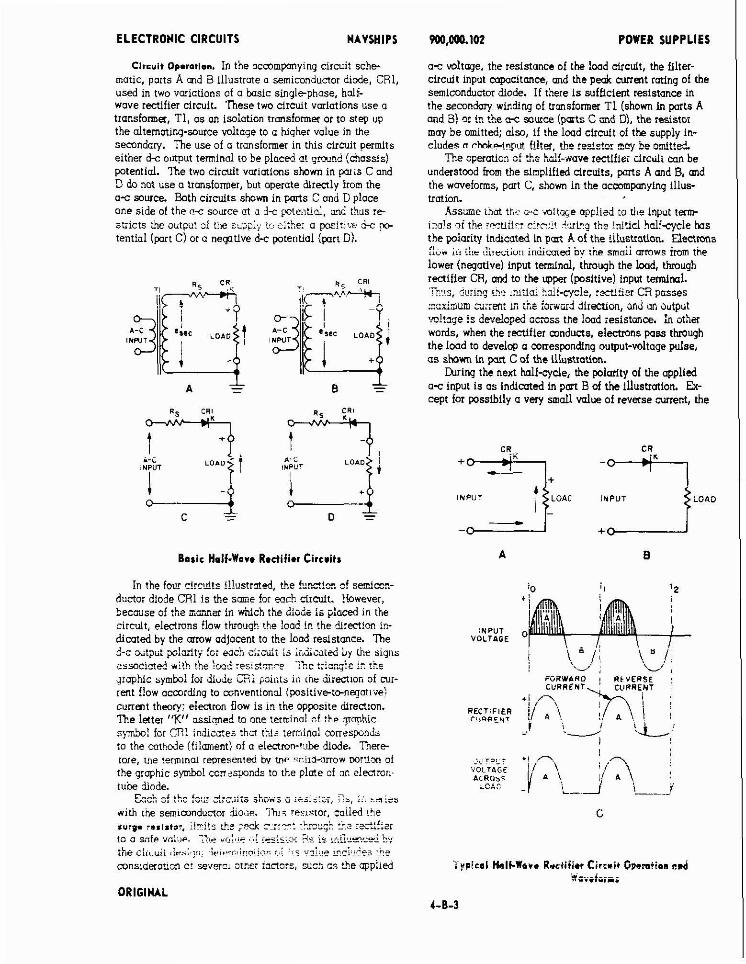
ELECTRONIC CIRCUITS NAVSHIPS
Cttsuit Op.rotion. In the accompanying circuit sche- matic, parts A md B illustrate a semiconductor diode, CR1, used in two variations of a basic singlephase, half- wave rectifier circuit. These two circuit variations use a transformer, TI, a s m isolation trmsformet or to step up the alternating-source vuitage to a higher vaiue in Ule semndarv. ?he use of a t r~sformer in this circuit D€Tmits either d< output terminal to be placed at grxnd !rhass!c) potential. ?he two circuit variations shown in pm;s C and D do not use a trmsformer, but operate directly from the 0% s w c e . Both circuits shorn in pmts C and D place one side of the c i source nt a is ptrntia!, md thus r e suicts the outpu! s! the s;pp:g :c ei:he: a positjw ;f 9 tenth1 (part C) or a neqtive d-c potential (port D).
CRI
. ~
a-L
'7Y. L O
--y3 - D =
Basic Half-Wave Rectifier Circuits
In !he !OLE d r c d t s !!!nstrc!ed, the !sncioz c! s d c c ? ; duaor diode CR! i s the sane !or each ciroltt. kbwever, because of the -ma la r h i i h ;:,e di& is placed in ihe circuit, electrons flow through the load !n the dirmion 1.; dicated by the mrow adjacent to the load resistmce. 'lie d-c xtput plariti. fi.1 sih G;Mt is ;idii7l[ed by Lhr aigns ~ssocioted rl!h !be em:! :eelst-cc~ ?e rrianqie :: :5e graphic symbol for d i d e CZ; i;oii;is ii; ine direcfzon of cur- rent flow amrding to mnventional (positiverc-negatiiie! cunmt theory; electron flow i s in rhe opposite direction. m e lecter "K" assiqned to one terminal cf !he grmhir s y n h ! !or CR! indicates that t:Js teminal corresponds to the cathode !filament) of a electron-b~be diode. There- lore, me lemlnai represented by Vlr. ~:rilC-Jnow mr!!tn o! the graphic symbi consswnds to the plate of CG elecimn- tube diode.
C--L-',,.-'-,.. d -L - : . - : -.-- ?. ,. , -Ill "1 ,..& ."". - L , I Y I L 1 >II""O Y .C3._.L.ll I : > I ' i t L c X i S S
with <he smlmndunor dolie. Th?i ve.istor, caiied !?e rurs. -..!st,;, l!!?!!s :be ;I& 2::-: :Lx-;> 5-2 :&;!ir to o w l e vni;,e. -ii ..::,LC . .i iesizi2< ?- ir I:~~X"I.I;& h,: .L . . . . . . . , .
~i,,."i( . i ?,,. . c , > , > ~ , ~ , ? , : ?~.; .t: ug!.:,e L"c!:LZes :!!s mnsidanuon e! sevwa 31r.E: i"rctofc, such a s the applied
WO.Wa.102 POWER SUPPLIES
a c m l t q e , the resistance of the load circuit, the filter- circuit input cawdtance, and the ~ea!t currmt ratina of the semlcond~~nor liode. If 12e:e is sufficient resistance In the s e m n d w w~r+n? ?f trxsformn T I (shown In pmts A m d 8) or I . ib.e c-c &wce (parts C a d id), the resistor may be omitted; also, if the load circuit of the supply in- cludes n cWe!cpm (I!!lx, the res!s*r mF; he o~l:!e;t
9.- opaation of b e half-wave 1%-ifier d r c d l con be understood from the simplified drcuits, pans A and B, md the waveforms, pmt C, shown in the acmmpmylng illus- tration.
Assme that tr.? cc a l t sye appiied io tire input t m - imis ni the ie-xif!rt ci,~..:ir ilni-g the !niticl hdfsycle hos the polarity indicated in pmt A of the !ilustratlon. Elenmns Zvn 111 ;he t;i:r~iiu:: i n d i m & bv ine smoii mows i m m tne lower (negative) input terminal, through the load, through rectifier CR, ad to the upper (positive) input termlml. '%IS, dunng L?? ~9~11.1: kd!-cycle, r w S c r CR passes r.oxirnG cdcw,; si t i € isiwmd d i i e ~ ~ u n , and an output vo!!qe i s devdoped o a s s the load resistace. 3, o t h s words, when the rRtifier mnducts, electrons pass through the load to develcp a corresponding output-voltage pulse, as shown in p a t C of the illustratlan.
k i n g the next half-cyde, the polarity of the applied a-c input i s a s lndimted in pmt B of the il lusuaion Ex- cept for pss lbf ly a very a n d d u e of reverse current, the
INPUT INPUT t LOAD
I N P U T V O L T 4 G E
RECTiFlER C < ! D O E ~ '
ORIGINAL
ELECTRONIC CIRCUITS NAVSHIPS
rectifier does not conduct, the reverse resistance remains high, and the small current which flows con be neglected. (Normally, the reverse resistance of the rectifier 1s exireme- ly high a s compared with the circuit load resistance.) Thus, during the secund half-cycle, no voltage i s developed across the load resistance. In other words, becouse the rectifier i s nonconducting and no electrons pass throuqh the load, there i s no output from the circuit.
The waveforms given in port C show that, on positive holf cycles of the applied voltage, current passes through the rectifier and the load resistance, pmducing an output voltoge across the lood resistance. The output voltage hos a pulsating waveform, which results in an irreguiar!y shap- ed ripple voltage; the i r q u e n q of the r i p l e voltage i s the some a s the frequenq of the a-c murce. Since the output voltage and current are m t continuous, the half-wave mti- f i n circuit r q u r e s considerable filtering to smmth out the ripple and produce o steady d s voltage.
The peak inv.r.. voltage of the semiconductor rectifier 1s defined a s the maximum instantaneous voltage in the direction opposite to that in which the rectifier is designed ta pass current. Assuming the output of the supply to be filtered, the peak inverse voltoqe across the rectifier in o half-wave rectifier circuit during the period of time the rectifier i s nonconducting i s approximately 2.83 times the rms value of the applied (or transformer secondary) voltage.
The output of the half-wove rectifier circuit is connect- ed to a suitable filter circuit, to smmth the pulsating dir- ect current for use in the load circuit. (Filter circuits are discussed in Part D of this section of the handbook.) Be- cause of the very low forword resistance of the semicon- ductor rectifie and its asmcioted low internal-voltage drop which i s practically independent of load current, the half-wave power supply iincludlng filter and load) using a semiconductor &ode will have somewhat better requlation characteristics than the equivalent electron-tube =ircuit; however, the raulotion i s still considered to be relatively pwr.
FAILURE ANALYSIS. No Output. In the half-wave rectifier circuit, the noout-
put condition i s likely to be limited to one of several pos- sible muses: the lack of applied a-c voltage (including the possibility of an open series resistor Rs or a defective transformer), a defective rectifier, or o shorted load circuit (including shorted filter-circuit components).
The a-c supply tZ.ltoge should be measured at the input of the circuit to 2,;-r;>ir.e whether the voltoge i s present and i s the mnect value. If the circuit uses a stepup !:. isolation) transformer, measure the voltoae at the secundorv terminals to determink whether it i s presint and i s the mr-' rm value. If necessary, the primary voltage should be removed from the transformer and continuity measurements of the primw and smndarv windinas mode to determine whether oneof the windings i s open, since an open circuit in either winding will cause a lack of secondary voltage.
If the circuit includes o series resistor (Rs), a resist- ance measurement can be made to determine whether the reslstor i s open. However, if the resistor i s found to be open, the rectifier and load circuit should be checked fur- ther to determine whether excessive lood current or a d e
900,000.102 POWER SUPPLIES
fective rectifier has caused the resistor to act a s a fuse and to open.
With the a s suppiy voltage removed from tne input of the circuit and with the load disconnected from the rectifier. resistance measurements can be made across the load to determine whether the load circuit (includinq filter compon - ents) i s shoned.
Although physicol appearance 1s not a positive indica- tion of condition, the rectifier may be given o visual check for a change in physical appearance which con indicate rectiHw failure. A relative check of the rectifin condition can be made using on ohmmeter, a s outlined in a previous paragraph of this section. However, failure of the rectifier may be the result of other causes; therefore, additional tests of the filter and load circuit are necessary. Once the filter components and load circuit have been determined to be satisfactory, o procedure which can be used to quickly determine whether the rectifier i s defective i s to substitute o known nmd rectifier in the circuit ond measure the output voltage.
L o r Outout. R e renifier should be checked to deter- mine whether the low output i s due to normal rectifier aging. A relative chec* of the rectifier condition con be made us- ing an ohmmeter, a s outlined in a previous paragraph of this section. If the forward resistance of the rectifier in- creases, the output voltage will decrease. Also, if the reverse resistance decreases, the output voltage will d e crease, and the ompiitude of the ripple voltoge will b m m e excess1 ve.
The load cunent should be checked to moke sure that it i s not excessive, because the circuit has relatively w r regulation and an appreciable increase in load current ( d e crease in lwd resistance) can muse a decrease in output voltage. Also, the filter circuit components should be sus- pected a s a possible muse of low output. Once the lwd circuit and filter components have been determined to be satisfactory, a procedure which can be used to uuic!dy determine ihether the rectifier i s at fault i s to iubstiute a known good rectifier in the circuit and measure the output voltage under normal load conditions.
SINGLE-PHASE, FULL-WAVE RECTIFIER.
APPLICATION. The single-phase, full-wove rectifier i s commonly used
in all types of electronic equipment for applications requir- ing high- or low-voltage dc at o. relatively high load w e n t . The rectifier circuit can be arranged to furnish negative or positive output to the load.
CHARACTERISTICS. Input to circuit i s ac; output i s dc. Uses two semiconductor rectifiers Output requires filtering; d-c output ripple freqiency i s
twice the primary line-volfoge frequency. Has gmd regulation characteristics. Circuit provides either positive or negative-polarity out-
put voltage. Uses power tronsformer with center-tapped semndary
winding.
ORIGINAL
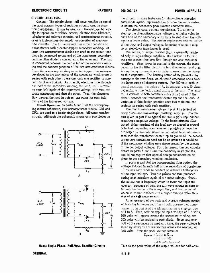
ELECTRONIC CIRCUITS NAVSHIPS
CIRCUIT ANALYSIS. General. The singlephase, full-wave rectifier is one of
the most common types of rectifier circuits used in el* tmnic equipment. It may be used a s a low-voltcqe d-c sup- ply for operation of relays, motors, electmn-tube filments, telephone and teletype circuits, and semiconductor circuits, or a s a high-voltoge d-c supply for operation of electrow t b e ci:=its. The $dl-wave rectifier drc;;it consists of o transformer with a center-tapped secondary winding. At least two semimnductor diodes are used in the a rmi t ; one diode i s mnnected to one end of the transformer secondary, and the other diode i s connected to the other end. The lmd i s connected between the center top of the semndav wind- ing w d the m m n junction of the two semimndunor diodes SirEX iilc >tiu,i&,y wi,,dirtq i* ~ c ! , i ~ l - L p & , ti,c ""ihp developed in the two halves of the secundory winding are in series with euch other; therefore, on!y one rectifier is mn- ducting at any instmt. As a result, electrons flow through one half of !he secondary winding, t!:e lmd. CR:! c :&tifir: on each half cycle of the impressed voltoge, with first one diode conducting and then the other. Thus, the electmns flow through the load in pulses, one pulse for each half c y d e of the impressed voltage.
Circuit Oporotios. In pmts A and B of the acmmpany- ing circuit schematic, two semimnductor diodes, CR1 and CR2, me used in a basic singlephase, full-wave rectifier circuit. Although the schematic shows only two diodes in
& s i r Si.plrPhas., FmII-War* Rwtl f in Ci~caits
WO,WO.lOZ POWER SUPPLIES
the c i r d t , in some instances for high-voltage opeation each diode symbol represents two or more diodes in series to obtaln the n e c e s q @-inverse chm.acteridics.
The circuit uses a single transformer, T1, either to step up the altenatinq-so~rce wltage to o higher value in each half of the semndory winding or to step down the volt- .:? !. a !ore. v d w . ?be drcd! q:!ir??inn nn? the vnlner 0: the input ad Oiiipui n k a g e s deteimine whethe a step- up or stepdown transformer is used.
The series, or surge, resistor (R.) is generally requir- ed only in highvoltage supplies. Its function is ~i limit the pffik current that con flow through the semiconductor rectifiers. When power is opplied to the circuit, the input copantor (in the filter circuit) i s in a discharged condition. ;. v r t y hmvv mnenr iicws ini~iniiy ro estdniis" ine ckkorge on this capacitor. The limiting anion of R. prevents any damage to the rectifiers, which would otherwise occw fmn the large surge of charging current. For 330-volt (p& in-
, ... ,=.--.- ,..- -. . . -- . L.una, ruvs ur x. is De:"?en : x,ir~ x oi~xs,
iependiE9 on :he s f f i k -.,- -+ -A'-- - 6 +t, ..-'a .~,e.., .,...,, ,. ,, e ,.... 3 e resis- tor i s common to bdh rectifiers since it i s placed in the circuit between the transformer center tap and the laad. A variation of this design practice uses two resistors, one resistor in series with each rectifier.
The circuit arrangement given in part A i s t y p i d of many plate- and low-voltcqe (positive) supplies. The cir- cuit given in part B is typical for bias supply applicafions reqiring a negative voltoge. In the basic circuits Ulus- trated, either terminal of the load may be placed at ground I"!~!?!!E!, d q e n f i ~ : ~ Z E whe!hei I positive N n q e i v e G c output i s desired. When :he d-c output terminal associ- ated with the transformer center tap i s grounded, the second- ary-twore insulation need not be a s great a s it would be if the secondary windinu were above mound bv the mount of the d c outp"t wltag;. For thls rwson, the two circuits shown in pans A and Bare the mmmonlv used drcults. and do not require that special design c&sidaation be' given to the secondary-wlnding insulation.
In parts A and Bof the ocmmpanying illustration, the i -okqe inJuced ;ir illch hd: of the secondary of tiansfoimec T I causes each diode to mndun on alternate half-cycles of the input voitage. Two d c puises me thus produced 3i;ring wch complete cyde of :i input voltage. Hence, the output has o frequency which i s twice the input f r e quenq. &cause oi .Ibis, Ihe fuii-wave circuit i s more et- ::;:en:, hos Se::ei ioitoge ;qdoliort, and hos oir output whlch is Rlsler to fiiter!wlth n htgher overoge value thm tho! "! !he h.qif-rcve cii"dr/.
As on example of the peak and werage voltages sbtdn- e.' !%, l i e (I:!!-w-.!a ~ ~ .pr+i!ipr ~.~~~~~~~ -/lz:!(, ~~~ ZZS!A-? !LC! t 7 . l ~ -
~. ~
. :orme; I I in pm A 0: a e i i i u s i i a t i ~ ~ hos o 5:-yp iatlo of 1 to 6. Then, with on opplled !a:,* uo!!age of 1!5 d t s , 690 volts will oppea across the secondary winding, and 415 volts will be applled to each diode. Since only one- half of the secondw i s used at o time. the D& voltwe i s . . iound by using k i f oi the voitage across the windtnq, or 345 volts. Fmm the D& voltaae formula: -
=pe.k = L4i4 x Em. - : A > " .. 7 ° C - '..,... . ",, . ""Q ..->.- , ---.. > - -,<, ,,,,,,. ,,,,,,,,"".
This is the @ value of the output voltaqe for half-wave
4-8-5
ELECTRONIC CIRCUITS NAVSHIPS
(s inqlepdse) recuilcT13r.. jlnce lwc piises ore p:duc& 131 every cycle of w lr.p~t vo!:age in f i l - w ~ v e r e n i l ~ r ~ t l o n . the overage value of the d-c output voltage will be greater than that for half-wave rectiLimtion; thus:
= 310 volts (mmx)
In a fullwave rectifier circuit designed to furnish high- voltage dc to the lcad, the peak-inverse voltage rating of the semiconductor rectifier i; Jn important consideration.
The peak-inverse voltoge across a semiconductor recti- fier in a full-wave circuit during the period of time it i s nonconducting i s approximately 2.83 times the rms vol tqe across half of the transformer secondary or a p -
L
proximately 1.41 times the rms voltage across the entire secondary (e..=). For high-voltage applicotions, several identicol-type rectifiers may be placed in series or stacked to withstand the peak-inverse voltage and avoid the possi- bility of rectifier breakdown. Generally, whenever a single rectifier unit i s used in the full-wave circuit, it i s chosen to hove a peak-inverse voltage rating which is conservative and thus provide a safety factor.
Because of the very low forjvord resistance of the semi- condwtor rectifier and its low intemol-voltoge drop which i s practically independent of load marent, the full-wave power suppl; using semiconductor d i d e s hos regulation characteristics which opproach or equal those of the equi- valent electron-tube circut usitiq mercury-vwr rectifiers. Hence, i ts regulation characteristics are somewhat better than those of the electron-tube circuit which uses high- vacuum rectifiers.
FAILURE ANALYSIS. No Ourpvt. In the full-wave rectifier circuit, the noout-
put condition i s likely to be limited to one of several pos- slble causes: the lack of m ~ l i e d a s voltaae (indudina the . . pcss~btlity of a jefective transformer), defecrive rectifiers. or o snmed loac clrcult Onc!udlna swrted !ilteriirc>dt components).
The a-c voltaue applied to each rectifier should be . .. measured between the secondary center tap and each recti- fier to determine whether mltage i s present and of the cor- rect value. If the circuit includes a series resistor (Rs), an additional measurement should te made ketween the load connection ot the resistor and the rectifier to determine whether the resistor is open. (With primw voltaqe removed from the input, a resistance measurement can be made to determine whether the resistor i s open.)
If necessary, measure the applied primary vol tqe to determine whether it i s present and of the correct value. With the primary voitage removed from the circuit, a mntin-
9W.wO.102 POWER SUPPLIES
uity measurement of the primory winding should be made to determine whether the winding i s open, since an open wind- ing will cause lack of secondary voltage.
If the circuit includes o series (surge) resistor mmmon to both rectifiers and the resistor i s found to be open, each rectifier and the load circuit should be checked further to determine whether excessive load current or a defective rectifier(s) has caused the resistor to act a s a fuse ond to open. With the o-c supply voltage removed from the input of the circuit and with the load disconnected from the rectifiers, resistance measurements con be made across the Iwd to determine whether the load circuit (including filter components) i s shorted.
Although physicol appeamnce i s not a positive indico- tion of condition, the rectifier may be given a visual chedi for a change in physical appeamnce which can indicate rectifier failure. A relative check of the rectifier condition can be mode using an ohmmeter, a s outlined in o previous paragraph of this section. However, failure of the recti- f i e r ( ~ ) mav be the result of other causes: therefore. oddi- . . . tional tests of the filter and load circuit ore n e s i a r y . Once the filter components and load circuit hove keen de- termined to be satisfactory, a procedure which can be used to auicklv determine whether the rectifiers ore defective is . . to substitute known good rectifiers in the circuit ond meas- ure the output voltage.
Lex Output. h c h rectifier should be checked to deter- mine whether the low output i s due to normal rectifier a g ing or to one or more defective rectifiers. A relative c h e d of rectifier condition con be mode using on ohmmeter, a s outlined in a previous paragraph of this section. (A mm- p r i m oon ke m d e by checking one rectifier ap ins t the other to determine whether they have similor characteris- tics.) If the forward resistance of the rectifier increases, the output voltage will decrease. Also, if the reverse resistance decreases, the output voltage will decrease, and the amplitude of the ripple voltage will become excessive.
Since the full-wove rectifier circuit normally supplies current to the load on each half cycle, failure of either rectifier (or associated series resistor, if used) or an open in either half of the secondary winding will allow the cir- cuit to act a s a half-wwe rectifie~ circult, and the output voltage will be reduced acmrdingly. Furthermore, whenever this occurs, the ripple mnplitude will also increase, and the ripple frequency will be that of the a s source (instead of twice the source frequency). If one rectifier of the full- wave circuit i s found to be defective, rather than replace the defective rectifier only, it i s good practice to riplace both rectifiers ot the same time and to make certain that the replacement rectifiers have like, or matched, charocteris- tics.
With the primory voltage removed from the circuit, r e sistance measurements can be made to check the mntin- uity between the center tap and each rectifier terminal; this will determine whether one of the windings is open. As an ahemotive, the a s secondary voltoge applied to each rectifier can be measured between the center tap and each rectifier to determine whether both voltages are p r e sent and me of the correct value.
The primary voltage should be measured to determine whether it i s of the correct value, since a low applied pri-
ORIGINAL
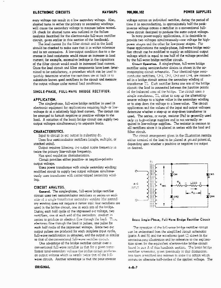
ELECTRONIC CIRCUITS NAVS~IPS
mary voltage can result in a low secondary voltage. Alsc, shorted turns in either the primary or semndnry windings will cause the secondary voltage to measure below normal. (A check for shorted turns was outlined in the failure analysis described for the elearon-tube hid-wave rectifier circuit, given earlier in this section of the handbook).
n~ >.-, - ..... ,.. .L. I,,.-. ;.... :. .- .L- ,""A, "15 ,""" Lullsllr ,," urs L L A L S I Y l L Y I L "2," I" l a i c rvvu,
should be checked to m&e sure that it is wiinin toieronce and i s not excessive. A lowvutput condition due to a de- crease in lmd resistance would muse an inaease in lmd current; irx example, excessive lmkage in the cwacitors of the filter circuit would result in increased load current. Once the load circuit and filter components have been deter- mined to be satisfactow, a procedure which con be used tc . ~ ~. yickly deterdne whether the rectifiers are ot tmllt ir to substitute known good rectifiers in the circuit and measure the output voltage under normal !wd mndit~ons.
jiNGiE-PHASE, F i i i i -WKiE BXiaZS RECTIFIEE.
APPLICATION. The single-phase, full-wove bridge rectifier i s used in
electronic wuioment for applications requirinq hiyh- or iow- voltage dc a'relatively high load current. f h e a r c u i t can be arranaed to f m s h nwative or positive voltage to tne load. A variation of the basic bridge circuit can supply two output voltages simultanmusiy to separate loads.
CHARACTERISTICS. !r: ci.rn,L! i. a.: ..!p.* i s p,Jsa!inn dc:
7 , c s e s four semimndunor rectifiers ( s in~ ie , mu!:ip!e, or stacked units).
Output requires fiitering; i - c output ripple irequensy is twice the primary linevoltage frequency.
Has good regulation characteristics. Circuit provides either positive- or negative-polarity
output voltage. Uses power transformer with single secondary winding;
modified circuit to supply two outpul voltages simu!tane- uusiy iiu,a;"iiile w i t .2 L S ~ ~ L S L - ~ ~ ~ ~ N --.'.. --.a D ~ Y l i U i l , ----- >--. ... niiii :-
ing.
CIRCUIT ANALYSIS. t m u o l . The single-phase, full-wove bridge rectifier
clrnut uses two semimnducror renrirers i n s a i e s un wuil . . . <>i a si ie t 22r,&f sKZTL $zy ,.;i:L:.;z {::,g s*T<z 5~
ory winding does not reqlrlre a center mpi: ioui rmiiiers are , . ,jsec ?n !he bridge circui!, one m ench ~ r m of f t8e ni14qe.
Zur in~ each half mcie of the impressed a c voitaqe, twa , r-i!iers; ole .t each en? n! !he +-nndoy mfdi!n i -
, , m orod~;e s i e n r ~ n I:L.w I~VOUQ"!~!~ ?I,,,
~imron ilow rhmuqh the iwd in pulses, one pulse for each half mcle of the impressed voitaqe. Since two d-c output pulses me prsduced for each mmplete input njcle, full-wwe rectification i s obtoined, and the output 1s simiim ro rhor oi iieconvcn~iunui iuii-wuvr iecii:irr ~ i ~ ~ u i i .
One advantage of the bridge rectifier circuit over a ianvenuond L C - ~ . . ~ , ..,. r; . LS : .L- z-. .u. - 9L~e : -;. ::G:s.
'--- *-*":<-"A"", ,.,.: ,,.,.- p;," ;,,;A,,- ,.;,,-,,;, 7,,.T"+,,,~,-. .-.--. .-.- ---.. , ""- 7.------ . . , . . . -2 0-t-c: \!citace .+hic. 2s !W?CP I"= "! i"P !i!?i.
wave circuit. Another advmtoge is tho? the pa - inve r se
900,000.102 POWER SUPPLIES
voltage across an individuol rectifier, during the period of time it i s nonconducting, i s approximately half the peak- inverse voltage across a reclifier in o mnventional full- wove ~ c u i t designed to produce the some output voltage.
in many power-supply appiicotions, it i s desirable to provide two voltoges simultaneously-one voltage for high- ~ w e ~ a;~yes mil: ;hi- i)ihi.i hi :~*.-,x*ei ~ 5 ~ s . Fci these appiicotions the singie-phase, fuii-wave bridge recti- fier drcuit can be modified to supply an oddltional output voltage which i s equal to one half of the voltage provided by the full-wave bridge rectifier circuit.
circuit O~uation. A sinqlwhase, full-wave bridge . . rectifier using semicmdunor diodes is shown in the ac mrnpanvino circuit schematic. Four identical-tpe semi. . . - ~ ~ f i d - 3 0 ~ r.*l:!iers, :.yi, :-.!di, CYJ ~ 2 6 p q , ,EF ,mnneci-
ed in a bridge circuit across the secondaw winding of traqsformer Ti. E:ch rectifier fcm3s one a r m of the bridge circiiit; the load i s mnnecled between the junction points oi iiie baiar~ced unns oi the hridqa. T~ie cirmii i i S S ir
singie inmslonnn, Ti, cittier iir siw "up the aliercatinq- source voltage to a higher value in the secondary winding or to step dowl the voltage tc. a lowervalue. Tne drcuit opplicatlon and the values oi the input and output voltages determine whether o stepup or step-down transformer i s used. The series, or surge, resistor (Rs) is qnemliy used only in high-voltoge supplies and is not normliy re quired in low-voltage supplies. ' h e resistor i s mmmon to all rectifiers since it i s placed in series with the load m4 filter circuit.
ma -i.-,i. - "*-a. " i . . ~ in thn i l l , , o m , , n n nnrm,,l. ..,~. ~... %"., -.-."b..,b,,. "..*.. ... ...- either remind oi the load tc be ylaced at yrocd ptential, depmhng upon whether a pos!tive or nqative d-c output 1s desned.
3, Qp~rot io- n! the !~:ll-wove bridge rectifier c !?x i ! can be understold iron the simplified sircbit schematic ( p a t s A a d 3) md the wweforms :part Ci shown in the occompmyinq iilustration and by reiermce to [he expion-- tion qiver, for the eqoivclent electron-tube bridge drcuit i a ~ n d in puii A cf t i i s hoiidMr_ s&i;r,. I-e basic br:?i;e
. . ...-. " "."-.-",-" ,=, ,,,,, =, ... ,,=,,.~~..-. .,..-,. ",~..""~.. '.. U.." "."""u".-,.. . . . ?,ZS bsec <x;:;%?L! zcz :e<r?xz ts Sk0.W t:,e SCt!32 ,:::ic: occurs on alternate half-cycles of the applied voltage. The
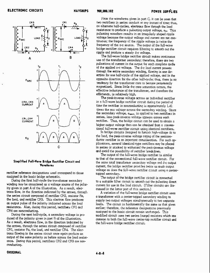
ELECTRONIC CIRCUITS NAVSHIPS
Simplified Full-Wave Bridge Rectifier Circuit and Waveforms
rectifier reference designations used correspond to those assigned in the basic bridge schematic.
During the first half-qcle the transformer secondary winding may be considered as a voltage source of the polar- ity given in pmt A of the illustration. As a result, e l e c trons flow, in the direction indimted by the mmws, through the series circuit composed of rectifier CR2, resistor Rs, the lwd, and rectifier CR3. This electron flow produces an output pulse of the polarity indimted acmss the load resistonce. Also, during this period, rectifiers CR1 and CR4 are nonconducting.
During the n e n half-cycle, a secondary voltoge is pro- duced of the polmity given in part B of the illustration. As a result, electrons flow, in the direction indicated by the arrows, through the series circuit composed of rectifier CR1, resistor Rs, the load, and rectifier CR4. 'Re e l e c trons flowing in the series circuit once ogoin produce an output of the sane polmity a s before acmss the load resist- ance. &ng this period, rectifiers CR2 and CR3 are non- conducting.
From the waveforms given in part C, it can be seen that two rectifiers in series conduct at any instant of time; thus, on alternate half-qcles, elemons flow through the lwd resistance to produce a pulsating output voltage, eo. This pulsating waveform results in an irregularly shaped ripple vo l tqe because the output voltage and current me rmt con- tinuous; the frequency of the ripple voltoge is twice the frequency of the a c sowce. The output of the full-wove bridge rectifier circuit requires filtering to smwth out the ripple and produce o steady d c voltage.
The full-wave bridge rectifier drcuit mokes continuous use of the transformer secondary; therefore, there me two pulsations of current in the output for each complete q d e of the applied a-c voltage. The d i load current passes through the entire secondary winding, flowing in one dir- ection for one half-qcle of the applied voltage, and in the opposite direction for the other holfqcle; thus, there is no tendency for the transformer core to become permanently magnetized. Since little d~ core saturation occurs. the . eff&ive inductance of the transformer, ond therefore the efficiency, i s relatively hiqh
The &-inverse w l t a i e across an individud rectifier in o full-wave bridge rectifier circuit during the period of time the rectifier i s nonconducting is approximately 1.41 times the m s voltage across the semndav winding. Since the smndary voltage, e..,, i s applied to two rectifiers in series, less peak-inverse voltage appears across each rectifier. Thus, the bridge circuit can be used to obtain o hiqher output voltaqe t h n con be obtained from 11 ccnven- tional full-wow rectifier cucuit using identical rectifiers.
In bridge circuits designed to fumish hiqh-voltoqe dc to the lwd, the peak-inverse voltoge rating ofthe semicon- ductor rectifier is an important consideration. For such ap- plications, several identical-type rectifiers may be ploced in series or stocked to withstand the peak-inverse voltage and m i d the possibility of rectifier breakdown.
The output of the full-wave kidge rectifier is similm to that of the conventional full-wave rectifier drcuit. For the same total transformer seco~dary voltage and di. output current, the bridge rectifier provides twice a s much outout voltage as does the full-w&e rectifier circuit using a center- tapped secondary.
The output of the bridge rectifier circuit i s connected to a suitable filter circuit to smwth out the pulsating direct current for use in the load circuit. (Filter circuits me d i s cussed in the latter part of this section.)
A variation of the full-wave bridge rectifier circuit uses a transformer with o center-topped secondary winding to supply two output voltages simultaneously to two separate loads. The circuit is fundamentally the m e 0s that given earlier; therefore, the reference designations previously assigned to the basic circuit remain unchanged. This modified drcuit uses two series (surge) resistors which me common to both the full-wove center-top rectifier circuit and the full-wwe bridge rectifier circuit.
ORIGINAL
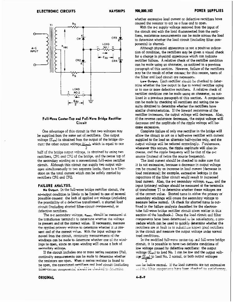
ELECTRONIC CIRCUITS NAVSHIPS
Full-Wave Center-Too and Full-Wove Bridge Rectifier Circuit
One advantage of this circuit i s that two voltages may be supplied from the same set of rectifiers. One output voltage (E.,) i s obtained from the output of the bridge cir- cult: the other output vo1ragelL.L which i s equal lo we
7 - hai! of the bridge o."p.?t -!~I!nge, i s ohtn!ned hy 11si"q two rectifiers, 3.1 and CR2 of the bridge, and t k c e n t a top Qi the secondary winding a s o m v m t i a n d full-wave rectifiet circuit. Although this cirmit can supply two output volt- ages simultonwusly :o two separate loads, t h a e i s n limit- ation on the total nurent which con be safely carried by r m i f i a s CRI and CR2.
FAILURE ANALYSIS. Ne Ovlp~1. In the fu l l r ave bridge rmif ier circuit, the
nwutput c o n d l t i ~ is likely to he limited to m e of sewmi possible causes: the lack of applied a-c vol tqe (including the possibility of a defective transformal, a shorted food =!:cult !including shnr .4 ti!terr!rcu!t m w e n t s ! : or defective recllflas.
The a-c semndarv volraae, e..~, shouid be measured S. the t:ansformer tam?nds to detam~ne vnetha ine voi tqe i s present and of the m r r m value. If necessary, measure the uppiled primav witone to aetermlne wnetner it is P r e sent and of the cmect voiue. With the input voltage r e moved from the circult. m n u u i t y measurements oi the windings can be made to determine whether one oi the xind- lngs is open, since an open winding wlll cause a la& of s ~ n A m wlraae.
If the clrcutt includes m e or m a e series resistors (Rs!: mntinuity measurements em be made to determine whether the resistors me open. W m o ser:es resistor i s found to be ow. . !'be n s d m d r-iiiers rind iood circuit i i t~c lud i i~~ . . . ~ . . . . , ~ .. , . > ~ UILer-CIILYLL '.,iUp,,,CiiiD, >INY_ YS i.IC-IF" iu ii.r.ii...,L
ORIGINAL
900,000.102 POWER SUPPLIES
whether excessive loud nurent or defmive rectifiers have caused the resistor to act a s a fuse and to open.
With the os supply voltage removed from the input of the circuit and with the load disconnected from the recti- fiers, resistance measurements can be made across the lcad to determine whether the loud circuit (including filter mm- wnentsl is shorted,
Although physlml appearance Is not a posltive lndlca- tion of condition, the rectifiers mw be uiven a visual check tor a change In pnysical appearan& whim can in&cote rectifier falure. A relative check of the rectifier mn&tiw can be made using an ohmmeter, a s outlined in a previous paragraph of this s d o n . Howeva, failure of the rectifiers may be the result of o t h a causes: for this reason, tests of the filter and load circuit are necessaw.
Lor Ournut. %ch i d f i e i s:fidd be i h d e d t; &la- -!:e whetha the !ow outpst i s due to nnnnal r ~ i f i e r aging or to one or more defmive r m i f i a s . A relative check of rectlller condition nm be made ustnq an ohmmeter, a s out- lined in a previous wraaaph of this section. A mmmrison can be made by ch&i& i 1 rmlfiers and mning the-re sults obtained to determine whether the rectifiers h v e similar chamctaistics. If the forward resistance of the rmifier increases, the output voltage will decrease. Also, if the reverse resistance decreases-?he output voltage will decrease and the amplitude of the ripple voltage will b e
~ ~
come excessive. Complete failure of only one rmifler in the bridge wlll
allow the circuit to act a s a half-wave rmifier with mrrerrt supplied to the load cn alternme h a l f q c l e s only, and the o"tput v o k q e w i l l t e rcxiucffi acmrdingiy. F~jy;.imo:e, whenever thls ormrs, the ripple amplitude will also in- n-se, nnd thp ripple f requmq will be that of the a-c source !!nstead of twice the source frequency).
The i w d m m t should be checked to make sure that it is not excessive, because a decrease in ontput vo l tqe can be m u s e bv an Increase in loud nlnent (decrease in load resistance); far example, excessive leak& i s the .madtors of the filter cirmlt would result in Increased iood ~ r r e n t Also, the c-c seaondary voltage, e..~, and the input (primary1 voltage should be measured ot the terminals of transfomer T I to determine whether these voltages me of the m r r m value. Shorted turns in either the primary on' secondary windings will cause the secondary voltage measure below rmrmal. (A check for shorted t m s i s out- lined in the failure analysis described for the electron- tube full-wove bridge rectifier dicd: yivm eari:er in iNs section of the h a n b k . ) Once the h a d clrcdit and fflter mmponmts 'mve been determined to be saiisiaduw, u p m cedure which can be used to quickly determine whether the reciifiers are ai fauii 1s to substii;;r i n i i ~ i : j . d r r r i f ier i in the c i r d t and meusure the out~ut voitme under numai ioad mnditlons.
!n the madified ful!-~m= ~MT-!?E. z:d fiil-wve bricke circuit, it i s possible to have twa definite candltions of law voltme caused bv defective rectifiers: the output w l t q e (Em! to loud No. I ccn be h w and !!!! output volt- c g e a t o !md No. 2 normal, or both output voltages
2
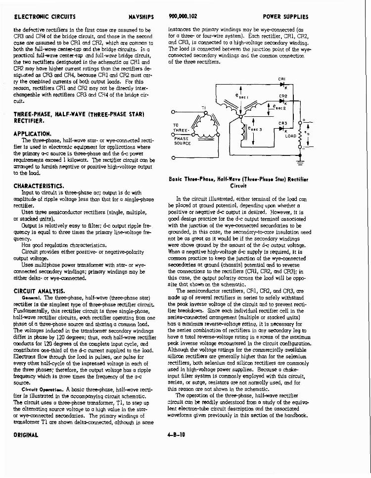
ELECTRONIC CIRCUITS NAVSHIPS
the defective rectifiers in the first case me ossmed to be CR3 and CRP of the bridge circuit, and those in the s m n d case are assumed to be CRI and CRZ, which me commn to both the Nl-wave center-top and the bridge circuits. In a practical full-wave centa+op and full-wove bridge circuit, the two rectifiers designated in the schematic as CR1 and CFO may have higher current ratings than the rectifiers de- sig~.oted a s CR3 and CR4, bemuse CR1 and CR2 must cor- ry the combined w r e n t s of both output loads. For this reason, rectifiers CR1 and CR2 may not be directly inta- c h a n g d l e with rectifiers CR3 and CR4 of the bridge cir- cuit.
THREE-PHASE. HALF-WAVE (THREE-PHASE STAR) RECTIFIER.
APPLICATION. The three-phase, half-wave star- or wye-cmnetcted recti-
fier i s used in electronic equipnent for applications where the prlmmy os source is three-phase and the d-c pwrer resuirements exceed 1 kilowatt. The rectifier circuit m be manged to fumlsh negative or ps i t ive high-voltage outplt to the load.
CHARACTERISTICS. Input to circult i s three-phase oc; output i s dc with
amplitude of ripple voltage less than that for a singlephase rectifier.
Uses three semicmductor rectifiers (single, multiple, or s t a d d units).
Outplt i s relatively easy to filter; d-c output ripple fre- w m c y i s equal to three times the primmy line-voltage fre- wency.
Has p a d regulation chmacteristics. Circuit provides either positive or negative-polmity
output voltage. Uses multiphase power trrmsfomer with star- or wye-
connected secondary windings; primary windings may be either delta- or wy-ected.
CIRCUIT ANALYSIS. G-mrol. The three-phase, half-wave (three-phase star)
rectifier i s the simplest type of threephase rectifier circuit. Fundammtdy, this rectifier circuit i s three single-phase, half-wave rectifier circuits, each rectifier opemtinq from m e phase of o threephase source and shming a common imd. The voltages induced in the transformer secondmy windings differ in phase by 120 degrees; thus, each half-wave rectifier oxducts for 120 deqees of the complete input cycle, md contritutes methird of the d-c current supplied to the load. Electrcns flow thmugh the load in pulses, one pulse for every other h a l f q c l e of the impressed voltaqe in each of the three phases; therefore, the output voltage has a ripple frequenq which i s three times the frequency of the a s m c e .
Clreult 0-tla. A basic three-phose, half-wave recti- fier i s illustrated in the accompanying circuit schematic. ' h e circutt uses a three-phase transformer, T1, to step up the alternating source voltage to a high value in the stor- or wyeconnected secondaries. I l e primary windings of transformer T1 are shown deltc-connected, although in some
WO,D00.102 POWER SUPPLIES
instances the primary windings may be wyffonnected (as for a three- or four-wire system). Each rectifier, CR1, CR2, and CR3, i s cmnected to a high-voltage secondary winding. l%e imd i s connected between the junction p i n t of the wye- connected secondary windings and the common connection of the three rectifiers.
C R I U
I A -'K
Basic Three-Phase, Half-Wave (Three-Phase Stor) Rectifier Circuit
In the circuit illustrated, either terminal of the load can be p l o d a t mound potential, dewndina u m o whether a . . * . p0;itive or n k t i v e d c output i s desired. However, it i s a d desim ~ract ice for the d~ output terminal asscciated i i t h the j k c t i m of the wy-e&ed secoodmies to he mounded. in this case, the secondom-tocore insulation need not be as. great a s it would be if the iecondary windings were above q~ound by the amount of the d c output voltaqe. When a negative high-voltage d-c supply Is required, i t i s common practice to keep the junction of the v e c m n e c t e d secmdmles a t ground (chassis) potential m d i o reverse the connections to the rectifiers (CR1, CR2, and CR3); in this case, the s t p u t p lmity across the iwd will be oppo- s i te that shownon the schematic.
'Ihe semiconductor rectifiers, CR1, CF2, md CR3, me made up of seveml rectifiers in series to safely withstand the peak inverse voltage of the circuit and to prevent recti- fier breakdown. Since each individual rectifier cell in the seriesccnnected ananaement (multiole or stacked units) . . has a maximum reverse-voltage rating, it i s necessary for the series combination of rectifiers in anv secondw lea to have a total reverse-wltage rating in excess of the'maGmum peuk inverse wltage encountered in the circuit configuration. Although the voltage ratings for the commercially available sillom rectifiers are generally higher than for the selmium rectifiers. both selenium and silicm rectifiers are commonlv used in high-voltage pwer supplies. k s e a choke-
'
input filter system i s commonlv emolwed with this circuit. . . . sk ies , or surge, resistors are not normally used, and for . this reason are not shown in the schematic.
The operation of the three-phase, half-wave rectifier circuit c a be readily understwd from a study of the eguiva- lent electron-tube circuit desnlptlm and the~asxr:ated voveforms yiven previously m mis section of the nonjbmk.
ORIGINAL
ECTRONIC CIRCUITS NAVSHIPS
For this reason. an exolmation of circuit operation is not given here.
The octicn of the semiconductor rectifiers in this circuit i s essentially the some a s that described for the equivalent electron-tube circuit. The rectifier in each secondow leu conducts for only onethird cycle, and this results in o series of d-c output voitaqe pulsations. Tne output voltage. e,, across the lmd resistance i determined by the instan- toneous currents flowing through the lmd; therefore, the output valtaqe never drops to zero because of the overlap cinq oi oc~l ied three-yn3se se:on?ni ,vo!t3qes 4 1 3 In? re s~ l t .nq rectl!ler :on?.c:.o, i n ecr? :wc:3i:y LC,;. 9e.lr.sr %e r.;ple ,v=kq.e !? ~ L I ! 12 ! ? r ~ ::-+s t . ~ !re;.er:v 3:
~ ~
the a c source, the circuit requires less filtering to smoath n ) ~ t the ripple "nd "nrdriilce o stead" d s vcltooe than 3oes 3
smgle-phase rectliier circult. The peak inverse ,vo!toge ocross the rectifier (multiple
or stocked units) in one secondary leg 01 the three-phase. holf-wove circziit during the period of time the rectlfler is nonconducting i s opproximately 2.45 times the rms voltage (e..,) across the secondary winding of one phase.
The regulation of the circuit is considered to be very a d . and i s better than that ai a sinaleohase rectifier * . > .
circuit hoving rquivalent powercutput roting; the semicon- ductor rectifier chorocteristics and the three-phose input con- tribute greatly to the improved regulation chorocterlstic of the supply. The output of the threephase, ha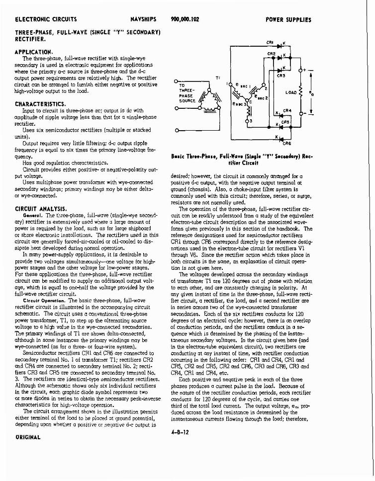
ELECTRONIC CIRCUITS NAVSHIPS
THREE.PHASE, RECTIFIER.
FULL-WAVE (SINGLE "Y" SECONDARY)
APPLICATION. 'Ihe three-phase, full-wave rectifier with singlewye
seomdary i s used in electronic equlpnent for applications where the primmy a s source i s three-phase and the d-c output power requirements are relatively high. The rectifier circuit can he mmnqed to furnish either negative or positive high-voltage output to the load.
CHARACTERISTICS. Input to circuit i s three-phase ac: output i s dc with
amplitude of ripple voltage less than that for a single-phase rectifier.
Uses six semiconductor rectifiers (multiple or stacked units).
Output requires very little filtering; d-c output ripple frequency i s equal to six times the primary linevoltage f r e ¶UenT.
Has g o d reylation characteristics. Circuit provides either positive- or nqative-polarity out-
put voltage. Uses multiphose power transformer with wyesonnected
secondary windings: primary windings may be either delta- or wyeconnected.
CIRCUIT ANALYSIS. G.n.r.1. The three-phase, full-wave (single-wye semnd-
awl rectifier i s extensivelv used where o larue amount of power i s required by the l&d, such a s for large shipbcard or shore electronic installations. The rectifiers used in this circuit me generally forceduir-cwled or oilemled to dis- sipate heat developed dwing normal opention.
In many power-supply applications, i t i s desirable to provide two voltages simultmmusly-one voltage for high wwer stoaes and the other voltaue for low-wwer staues. For thesebpplications the threephase, full-wove rectifier circuit can be modified to suoply an additional output volt- age, which i s equal to onehiif ihe voltage provided by the full-wave rectifier circuit.
Clrsult Operation. The basic three-phase, full-wave rectifier circuit i s illustrated in the accompanying circuit schematic. The circuit uses a conventional thtee-phahase power transformer, TI , to step up the alternating source voltage to a high value in the wye-connected semndaries. Tne primary windings of T1 ore shown delta-=onnected, althouah in some instances the vrimaiv windinus mav he . . vqGnnected (as for o three or four-wite system).
Semiconductor rectifiers CRI and CR6 are connected to secondary terminal No. 1 of transformer TI ; rectifiers CR2 m d CR4 ore m n e c t e d to s m d a r y terminal No. 2; recti- fiers CR3 and CR5 are connected to secondary terminal No. 3. The rectifiers are identiml-type semimductor rectifiers. Althouuh the schematic shows onlv six individuol rectifiers in the circuit, wch graphic diode bymtml represents two or more diodes in series to obtain the necessary peak-inverse
~ ~
characteristics for hiyh-voltage operation. The circuit arrangement shown in the illustration permits
either terminal of the 1md to be placed at wound potential, depending upon whether a positive or nyat ive d-c output i s
ORIGINAL
W0.000.102 POWER SUPPLIES
THREE-
SOURCE
CRI K I - 1
Bmslc Thm-Phase, Full-Wove (Single "Y" Secomda*) Rec- tifier Circmil
desired; however, the circuit i s commonly m g e d for a positive d c output, with the negative output terminal at ground (chassis). Also, a choke-input filter system i s commonly used with this circuit; therefore, series, or surge, resistors are not normally used.
The operation of the threephase, full-wave rectifier cir- cuit con be reodily undetstmd from a study of the equivalent electmn-tube circuit descriotion and the associated wave- forms given previously in &is section of the h m d h k . The reference desiunations used for semiconductor rectifiers CRI through ~ f f i correspond directly to the reference des ip notions used in the electton-tube circuit for rectifiers V1 throuqh V6. Since the rectifier action which takes place in both circuits i s the same, an explanation of circuit opem- tion i s not given here.
The voltages developed across the secondary windings of transformer T1 are 120 demees out of phase with relation to wch other, and are constantly changing in polarity. At anv uivm instant of time in the three-phase, full-wave r a i - . . fier circuit, a rectifier, the load, and a second reciifier are in series a n o s s two of the wyesonnected transformer seamdaries. Each of the six rectifiers conducts for 120 degrees of an electrical cycle; however, there is an overlap of conduction periods, and the rectifiers conduct in a se- quence which i s determined by the phasing of the instan- taneous s f f ~ l d a r v valtaoes. In the circuit uiven here land in the electron-tube equivalent circuit), two rectifiers are conductinu at m v instant of time, with rectifier conduction onunlng in tce ioiiowlng order: CRI md ZR4. CR1 and 3 5 , t'R2 and 3 5 . 3 2 ond '3%. JR3 and CR6. 3R3 and CR4, CR1 and CR4, etc.
Each positive and negative pwk in each of the three phases produces o current pulse in the lwd. Because of the nature of the rectifier conduction periods, wch rectifier conducts for 120 degrees of the q c l e , and carries one third of the total l w d current. The output voltoge, e., pro- duced across the load resistonce i s determined by the instantaneous currents flowing through the lmd: therefore.
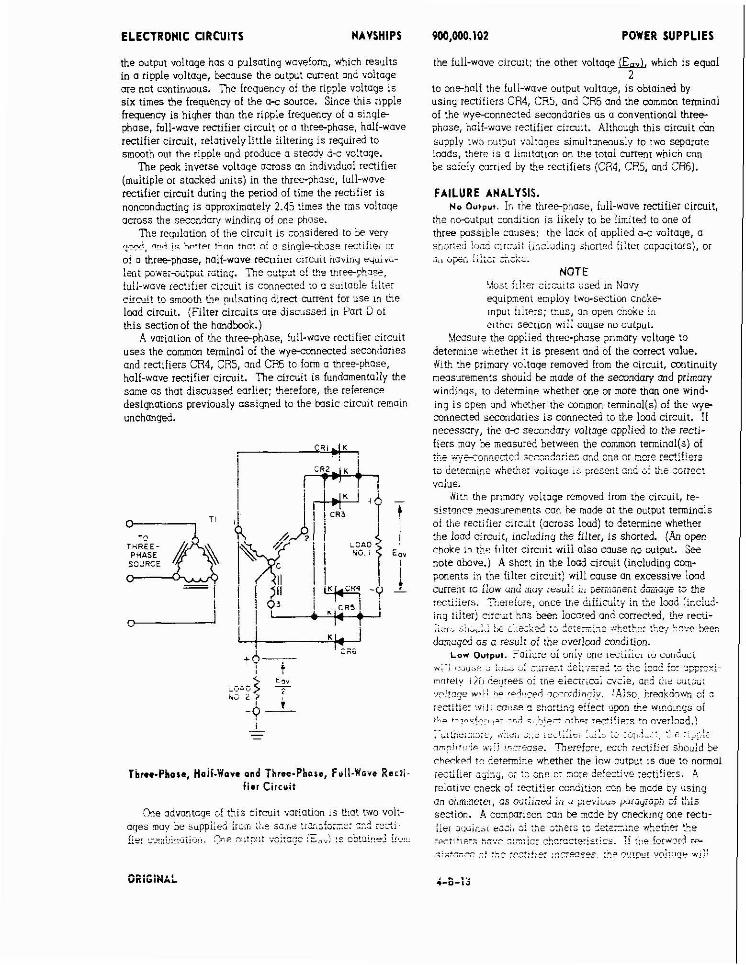
ELECTRONIC CIRCUITS NAVSHIPS
the output voltage has a pulsating waveform, which results in a ripple voltage, because the output cunent md voltage are not continuous. Tne frequency of the ripple voltage i s six times the frequency of the a s source. Since this ripple frequency is higher than the ripple frequency of a single phase, fall-wave rectifier circuit or u three-phase, holf-wove rectifier circuit, relatively little filtering i s required to smmth out the ripple and produce o steady d-c vo:toye.
Tne w o k inverse voltaqe across an indivld~al rectifier (multiple or stocked units) in the threrpb.nse, full-wave rectifier circuit durinu the period of time the rectifier is . ~
nonconducting i s approximately 2.45 times the ms voltoqe across the secondary winding of one phase.
Tne requlation of the circuit 1s considered to be very r : d , nnri !< h-tipi t w n that of c singleohose rectlilei or at o threephase, nail-wave recrliler uircull iluvilril cqwrj-
lmt ptieiii"twt A,,- ..'"..' "" .v*. " 4 ". '"D ............-... ' " ~ ~ ~ " h " ~ ~
iall-wave rectifier clrcult 1s connected !3 c silltuhlr filter c i rn~ i t tn smm!h !he plisoting diren NIIent for use in me Imd circuit. (Filter circuits are discussed in ?art 3 oi this sectionof the handbook.)
A voriation of the three-phase, full-wove rectifier circuit uses the common terminal of the wve-mnnected seconi'.aries and rectifiers CR4, CR5, and CF16 to farm o threephose. half-wave rectifier circuit. Tne circuit is fundamentoily the same as that discussed earlier; therefore, the reference designations previously ossiyned to the h s i c circuit remain unchanged.
Tire.-Phase, Hoii-Wave ond Three-Phase, Full-Wore Rciii i ier Circuit
One odvantoge of this circuit voriotion is that two volt- oyes muy be >~pp i l td irom ;ice s3.r.e ti;;,;!a;zi: ::.? rczti .irr...lll...l.lii. ,-t, .. ,-,.- A,..-... :r .. ," ";,,,;,,-: : ....... . . . ,.,.,- ......... ."..",.b ,--", ... ""
PW,000.102 POWER SUPPLIES
the full-wave circuit; tne other voltage which 1s equal 2
to one-holf the full-wave output voltage, i s obtained by usinu rectifiers CR4. CR5, and CR6 and the common terminal
sdpply two output voltages simuitmwusly to two separate loads, thete :s a !imltat:on on tne totoi currenr which con be safely carried by the rectifiers (CK4, CR5, and CR6).
FAILURE ANALYSIS. NO Ou+put. In the threephase, iuli-wave rectifier circuit,
the ncmutput caniiuon i s likely to be limited to one of three pss lble causes: the lack of applied o-z voltage, a sr,&rtfj l;~d arzuit ;i:,;i~dinq shortcd iiitet ;opacitors), or ;., "ps, i,l;;; ;;,;a;.
NOTE / I _ _ . i.,. , i._ v,uas rrr,c, r i i r d i t ~ xed in Noin, equipmenr employ twu-srctilx~ choke- mpu: ::i:ers; tnus, on open c n o ~ r in eirner secrlon w ~ i i cuuse oo output.
Measure the opplied threephase primary voltage to determine .#hetier it i s present and of the correct value. 'W!& the primory voltoqe removed !rom the circuit, continuity mwsurements should be made of the semndar/ md primary windings, to detemine whether one or more Vim one wind- ing i s open and whether the common terminolis) of the r y e connected secondaries i s connected to the lmd circuit. If necessary, the ai- secondary voltage applied to the recti- fiers may be measured between the common tetminal(s) of .'- .......-.. ... A ..-- ..A .:ar "" "". nr rmrti,ierc : : . . ....... " ....-. -..d ...................... .. --. . . ,u ;cLermine .*herher volt;ge .; p:eser' ..".." 7,: -1 -' ' h i x.- PC;'--' ?d..ZLL
ualue. 4113 the prlmary volrage removed from the circuit, re-
sistnnre measurements can he mode at the output terminals of .)- -.:<. . ". ". , , cc ie,,,,le. d r ~ s t (across lmd) to detemine whether the load circxt, including the filter, i s shorted. (An open choke 1" tne iiiter circoi: wiii aiso cause no output. see note above.) A short in the load circuit (including com- ponents in the filter circ?iit) will cause an excessive lwd curen< cc ilow 2nd muy ce>uii io pem?>~-~?fit ~ G Z G ~ S to :hs rcxtiliers. T:;rreioie, ooce k.e diiiialqy in the lsod (inti-2- ing 1;lterj n r c u t ?as 'ken locoted ond conened, h e recti- L r . , :A,",.:: & ~i,3:k& :z ? c ; e ~ , ; x .v:kct5c: :hi hc;? k e ~ damaged 0s a result of the overlmd condition.
L o r 0 ~ 1 ~ ~ 1 . o l i i l r e ai aniy urlr in;ll;i.l iu cu<~duit .., . .
" , , , 8 Z . J ,,,, ~: " ;,;>; 2: :,,;re:,: :s:.;e:si := r5c !3.?5 iz: 2~;:~::- . . mnteiy t20 toe<jrees 0, [re ekc rcLc~i cxcie , vllv --- ,.. u i e ~ ~ ~ + : .,-;t?,:r , w i i ?r r e d v ~ d or-nriinoli. . . !Also h r m k ? ; ~ ai ::
rectifier ,::;!i cn;:se c s?orU~"eiiec! u p o ~ toe w?ndlnqs ci t r , .l,?".f.~.~.i ?.? ; i , i n t ;:he; rrni!ie:s ?a a...er!ocd.! - . ......... , ,.,,-.... ".C, A:.-:. ;..c _c.:::.r. :-::: :. :> ! I ! - ' . . . . . . . . . 'ii -:--,- - . . nrn?i>:.,!i- xili !-,:rense. Inerefore. path. :ectifier silouid Se c'.pck~.i t l ?e!?nnine whether the tow aumilt 1s nue to normai ;ecs;ier a.. ,~n,, .. u, -- .- ,.. -r.c - o, . ...,, --. e A "e 'eec,,m .-...... ~ ~ ~ t i f i ers, n ;ciotl.ve i-heck o! recti!ier condition can Le made ay using an ohmmerei, as oriintri i n .i g~rviui;> paiuilizpk, of this section. A cammrizon con be made by checking one recti- iier aquinat CX!, c: 2,s ~ 2 , s : : ;z ?z:zr.::e ,w5%?e: :be
................. ...... ............... .- . , . - . . . ."... -.-., L, .. e . , n . m 7 ~ ~ p ; e ~ ; ? u I ! rl!r filiwi.! re- - 2 .LO ..,"...,o. ,.v-eme ,ha -,<, ",,, " ?,,,,, ",. .<!;: .,,.,, ..-..-.. ,.,,, . . . . . .............. .. .............. . .
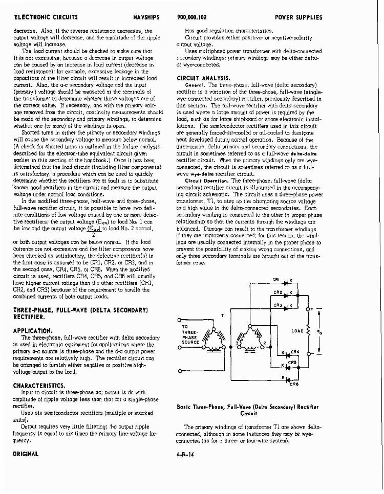
ELECTRONIC CIRCUITS NAVSHIPS
decrease. Also, if the reverse resistance decreases, the output wltage will decrease, md the amplitude of the ripple wltage will increase.
The l w d current should be chedred to moke sure that i t i s not excessive, hemuse o decrease in output wltoye car be mused by an increase in lwd NfterIt (decrease in lwd resistance): for example, excessive leakage in the mpacitors of the filter circuit will result in increased iwd current. Also, the os secondary voltoye and the input (primary) wltage should be measured at the terminals of the transformer to determine whether these voltages ore of the c o n e d value. If necessary, and with the primary volt- age removed from the circuit, continuity measurements should be mode of the secondary a d primmy windings, to determine whether one (or more) of the windings i s open.
Shorted turns in either the primory or secondary windings will muse the secmdary wltaqe to measure below normal. (A check for shorted turns i s oillined in the failure analysis described for the eleman-tube equivalent circuit qiwn earlier in this section of the hadhook.) Once it hos been determined that the lwd circuit (including filter components) is satisfactory, a procedure which mn be used to quickly determine whether the rectifiers are at fault i s to substitute 'known good rectifiers in the circuit and measure the output voltage under normal lwd conditions.
In the modified threephase, half-wove and threephase, full-wave rectifier circuit, it i s possible to have two defi- nite mnditions of low voltage caused by one or more defec- tive rectifiers; the output voltage (Em,) to lwd No. 1 can be low and the output voltoge&J-to load No. 2 normal,
7 . or both outout voltaaes can be below normol. If the lmd m e n t s ore not excessive and the filter components have been checked a s sotisfactorv. the defective rectifier(s) in the first case is assumed to'be CRl, CRZ, or CR3, and in the second case. CR4. CR5. or CR6. When the modified c i r a i t i s used, ;ectifi&s ~ k 4 , CR5, and CR6 will usually have hiqher current ratinas than the other rectifiers fCR1. CR2, and CR3) bemuse of the requirement to handle the combined currents of both output iwds.
THREE-PHASE, FULL-WAVE (DELTA SECONDARY) RECTIFIER.
APPLICATION. The three-phase, full-wave rectifier with delta secondary
i s used in electonic equipment for applications where the primary a s source i s threephase and the d c output power requirements are relatively high. The rectifier circuit can be arraqed to furnish either neqotive or positive hi&- wltage output to the lwd.
CHARACTERISTICS. Input to circuit i s three-phase ac: output i s dc with
amplitude of ripple wltage less than tho1 for a singlephase rectifier.
Uses six semimndsctor rectifiers (multiple or stacked units).
Output requires very little filtering; 1-2 output ripple frequenq is equal to six times the primary line-voltage f r e quenw.
W0.000.102 POWER SUPPLIES
Has gwd regulation characteristics. Circuit provides either positive or neyotivepolority
output wltaqe. Uses multiphase power tronsiormer with delto-connected
secondmy windings: primary windings may be either delta- or wye-cunnected.
CIRCUIT ANALYSIS. Gensrsi. nlhe threephase, full-wove (delta secondary)
rectifier i s o variation of the threephase, full-wave (single- wye-zonnected secondary) rectifier, previously described in this senion. The full-wove rectifier with delto secondary i s used where a lorye amount of power is required by the lcad, such a s for large shipbwrd or shore electronic instal- lations. The semiconductor rectifiers used in this circuit ore qenerolly forceduircmled or o i l iwled to dissipote heat developed during normal operation. Because of the three-phase, delta priman. and secondary connections, the circuit i s sometimes referred to a s o full-wove d.ltodelm rectifier circuit. When the primory windings only are wye- connected, the circuit i s sometimes referred to a s a full- wove rrrd.lm rectifier circuit.
Circuit 0p.rmtlon. The three-phase, full-wave (delta secondary) rectliier circuit i s illustrated in the occompany- ing circuit schematic. The circuit uses a threephase power transformer, T i , to step up the alternating source voltage to o high value in the delta-connected secondaries. Each secondary winding i s connected to the other in proper phase relationship so that the currents thrauyh the windings are balanced. Damage can result to the transformer windings if they ore improperly connected; for this reason, the wind- ings are usually mnnened internally in the proper phase to prevent the possibility of making wrong connections, and only three secondary terminals ore brought out of the trans- former cose.
SOURCE
CRI - , K I m
Boric ThrerPhare, Full-Wave (Delta second^^) Rectifier Circuit
The primary windings of transformer T1 are shown delto- connected, olthough in some instances they may be w y e connected (os tor a three- or fourr i re system).
ORIGINAL
ELECTRONIC CIRCUITS NAVSHIPS
Semiconductor rectifiers CR1 and CR4 me connected to seamdary terminal No. 1 of transformer T1; rectifiers CR2 and CR5 are connected to sfandary terminol No. 2; recti- fiers CFl3 and CR6 me connected to s m d a r y terminal No. 3. ' h e rectifiers are iden!ical-type semiconductor rectifiers. Although the schematic shows only six individual r d f i e r s in the circuit, each qaphic symbol represents two or more dides in series to obtnin the necessary wk-inverse characteristics for high-voltage opemtim.
The circuit mangement shown in the iliustroticn permits either terminal of the lmd to be placed at ground potential, depending u r n whether a positive or negative d-c output is desired; however, the circuit is commonly arranged for o positive d-c output, with the neqative wtput terninol 31 GX:.~ ( k z c c i ~ ) . P.!Ec, ? ~ h c k e i ~ ? ! f i i t e +?stern i n commonly used with this clrcuit.
Tne owrotion oi the three-phase, ~YIL-HTVF (&::a S?EZ<-
my) redfler circuit can be readily uaderstmd from a study of :he q ~ i v a l a t e!e-nc-!uk cirmit desc~iptim "nil the asscclated waveforms given previously in thls s d o n of the hoodbook. ?he reference designations used ' semi- mductor rectifiers CR1 throuqb CR6 coriespa~ .ectly to the reference designations used in the electron-tube circuit for rectifiers Vl through V6. Since the rectifier action which takes place in bath circuits is the m e , an explanation of circuit operatial is not given here.
Tne operation of the delta-secondary rectifier circuit is slmilar to that of the we-seamdarv rectifier circuit (me- viously described); however, the w voltage across an in- dividual deltoionnected s m d a r v windina is oooroximatelv * . . !.7? Umes geoter than the voitaqe across m! im!viduoi ye connected secondav winding for equal dz output voltages irom the two circuiis. W; tG,+~ J-~.-1---2 .LO L urvcIUp- UL~Y-* Y.Z
sffoodmy windings of uansformer T l are 120 degrees out of phase with relation to one another, and are constantly chang- ing in polarity. In the deltasmected semnday, at any giwn instant the voitage in me phase is equal to !he vector sum of the voltages in the other two phases. At any given Instant of time in the three-phase, full-wave rectifier cirmr, a r d f i e r , the lcad, w.d = s m . d rejfier n E Ln series across two terminals of the deltmmuected seandarles. Each ol the sin rectifiers cmducts for 129 d-s of a~ electrid cycle; however, there is m overlap of mnduction perlais, and the rectlfiers conduct in a sequence which is
by he - .. - c L - r - ."- ...- :,o.;nu ". tie ul~~u...u.m~ s m d w y .._$.__ U L L L ~ ~ ~ of <ie ;rrz: ';l-sfma. i- II.9 .irm1(? 5;- heie (and in the eiectrm-tdbe equimiwt ciicuit;, two ~ e c t t f ~ ~ i s ore mnductin~ at ar,v instant of time. with rectifier mduc- tim - h i m the~foliowinq order: CRi and i%, CM .113 CP.2~ CR2 mrl CRA. CRA md CR3. CR3 and CR5. CF.5
~ ~
snd CHI: CR1 a d 3% eti, Eoch positive and neqative peak in each of the three
phases produces a current pulse in tne imd. b s e of the natute of the rectifier conductlm periods, each rectifier anducts for 120 degrees of the cycle, md nrnles one third o e i i " , - - . 7 . " "d..d
ills " u r ~ l . u . L u y r , r".
a m s s the lcad resistance is determined by the instantaneous cunmt flowing thmughthe I d : therefore, the outp~t voltage hoe o +.ztt?; rcue!onn, uh!ih IPFII!!~ I" III/w!~ ~! tage , b a s e the output cArnt ad voituqc ore t~ui it.tthuu~s. R e frequency of the rippie ~ l t a g e is SIX dmes the irequency
900,000.102 POWER SUPPLIES
of the ( 1 ~ source. Since thls ripple frequency is hlghn than the rippie frequency of a single-phase, fdi-iave recllfia cirmit or a threephase, half-wave rectifier circuit, relativ4 ly Uttle filrering is required to smmth w t the ripple and produce a steady dc witage.
T1.e pok inverse voltage across m individual rectillm (multip!e or stacked units) in the three-phase, fdl-wave ideita secadmyj rniiiin ci1cmit duiiiiq the at 'Ae the rectifier i s omconducting is approximateiy 1.42 h e s the rms voltage across the seandary winding of me phase.
' h e regulation of the circuit is mnsidered to be very gmd, and is better than that of a singlephase rp t i f ie or of a three-phase, half-wove rectifier circuit having equlvrrlent power-output rotinq. 'he wtput of the threephase, full wave rectifier ciizdt is connected to a suitable filta dr- ~ a i t LG SEW?, Z z ;dsctL;~ &re. ~ 3 . t !of use in the !md c i r m i t - (Fiiter drcults arc discussed in Pat D of thls section i i h e hm,dhi~,r.j
FAILURE AMAL:;IS. n. 0-w. in me three-pnase, iuii-wav. ideira sgm&ryj
rectifier cirmit, the nooutput condition is Wtely W be limlted to one of three possible causes: the lack of applied c-c voltage, a shorted lwd circuit (Including shoned fllter mpa- citors), or an open filter choke.
NOTE Most filter circuits used in Navy equipment employ tw*section choke- input iilters; thus, m open choke In either sedon will crmse no ouQut. ... . . . +..' .." ' ..--. .-". 3 I .* - -2--~, .
'Llr ucs ,.r.uru, .u..r.,. .","".-a urn iiic ii:i...:, C,C-2-
tinulty measurements snwh be mode of the seccndary and nrlrnnry windinas to determine whether one a mae than me w!ndlng is q x n . Slnce the three windings of the delta- secondary circuit me metlines mnnected internally and only three :erminais are brought out of $e case, witage and resistance menswements are mode between the terminals of the delto-connected semndaries. When maklng measurements (wltage or resistance) of ".e secmdaq ckmlt, it should be remembered that the windlngs form a delta cmfigumtim, wlth two windings in serles, and this oomblnaUm In pamllel with the windina under measurement. In othe instances, the s e a m d q w!ndinys are connected m slx individual 1-1- nals, and these terminuls are m e c t e d iqpthcf to fam a delta mfiyration. Tnus, in this instance, the terminal rn-omtwis mny k removed to enable meusmmts w be m l d ~ M \ndivimmi r ~ l m d c q nictdinqs, irtdependent of other wfi&rys. if necessary, h e G; .milaye st each of the three hi$-voitoqe semnaar!es may w mwsurm betwem me terminals of the deltmxnnected smdar ies , to determine vnrtner voitnqe lib aresrni ma J; me L ~ R I miye. A h , if necessary, measure the applied t h r m a s e plmary voit- ZJE t i deted1e whefker !! is pesmr end of the Lnnrci d u e .
With the orimmv voltaae removed bw the circuit. resist- mce measur&ent; CM & made at the output terminks of the rectifier circuit ( a ~ o s s I d ! to detmdne whether the icad circuit, inciuig the fliter; is shorted. (AS ~ ~ p h i d ["he p d n g note, an open choke in the filter c l r r l t Y!!! "1% -JSP 1" "crp~!.) A s b r i in ihe mmpinnl~ oi
. . . . Ute "A& LULU. <L~'LZU&'< 2 i & b;.bL:;. ..;: ,-":.: :<, 2x222
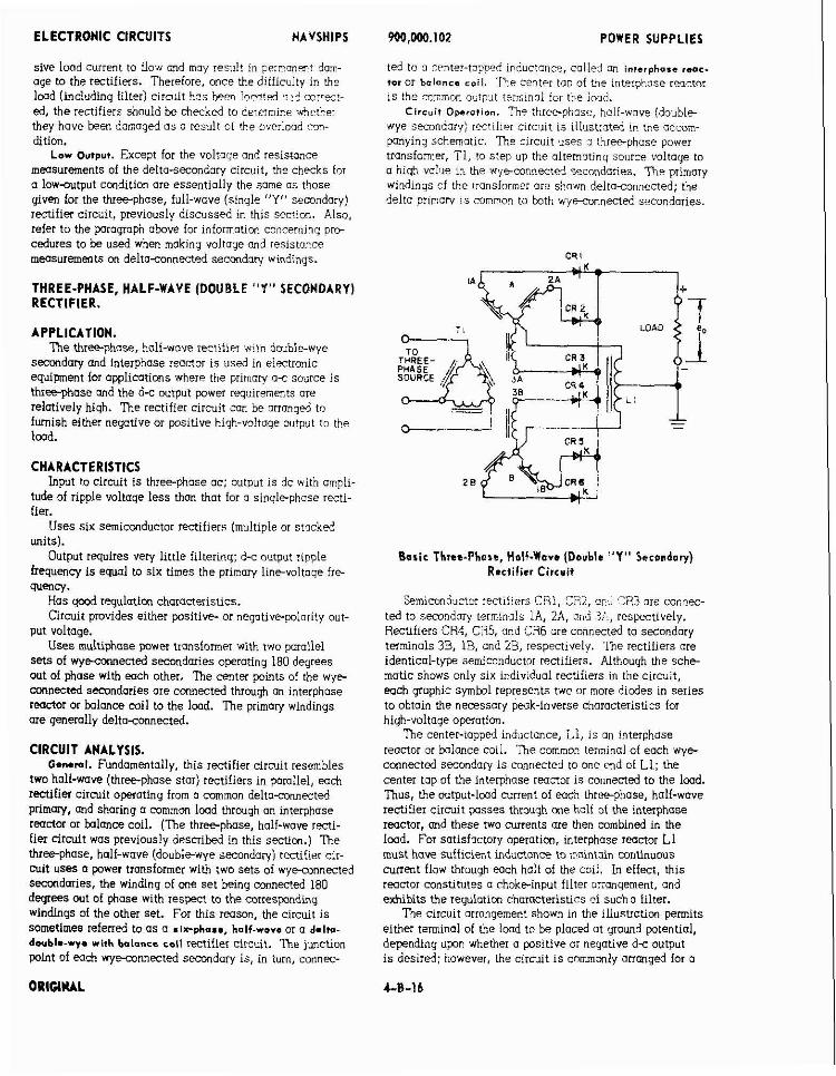
ELECTRONIC CIRCUITS HAVSHIPS
sive b a d current to flaw and may result in p~:-an-! dom- age to the rectifiers. Therefore, once the difficul:y in the lmd (including filter) circuit hcs ipm l ~ c g t d ,:!< COITCT!.
ed, the rectifiers should be checked to determine vhpther they have been donoqed a s a result of the overload z~n- dition.
Low Output. Except for the voltage and resistance measurements of the delto-secondary circuit, the checks fir a low-output cmdition are essentioiiy the same os those given for the threephase, full-wave (single "Y" secondory) rectifier c i rc~i t . previously discussed in this section. Also. refer to the pmagraph o h v e for informotion corcerning prw cedures to be used when making voltage and resista,nce measurements on deltaconnected secmdav whdings.
THREE-PHASE, HALF-WAVE (DOUBLE "'I" SECONDARY) RECTIFIER.
APPLICATION. The three-phase, half-wove rectiiier with double-wye
secondary and interphase reactor i s used in electronic equipment for a ~ ~ l i c a t i o n s where the orimorv a s source is th~&phase md the d-c output power iequirements ore relativelv hiah. The rectifier circuit con be orranoed to . - furnish either negative or positive high-voltage output to the load.
CHARACTERISTICS Input to circuit i s three-phase ac: output is dc wiin omp!i-
tude of ripple voltage less than that for o sinyle-phase recti- fier.
Uses six semiconductor rectifiers (multiple or stocked units).
Output requires very little filteriny; d-c output ripple frequency is equal to six times the primary line-voltoqe fre- wencl.
Has gaod ryula t im characteristics. Circuit provides either positive- or neyotive-polarity out-
put voltage. Uses muhitiphase p w w transformer with two porallel
sets of w y e c o ~ e c t e d secondaries operating 180 degrees out of phase with each other, The center points of the wye- mnec ted secondaries are connected through an interphase reactor Or balmce coil to the lmd. The primary windings are generally deltaconnected.
CIRCUIT ANALYSIS. Genoml. Fundamentally, this rectifier circuit resembles
two half-wave (threephase stor) rectifiers in pamllel, each rectifier circuit operating from a common deltaconnected primary, and sharing a common load through on interphase reactor or balance coil. (The three-phase, half-wave recti- fier dtcult was previously described in this section.) The three-phase, half-wave (double-wye secondary) rectifier cir- cuit uses a power transformer with two sets of wye-connected secondaries, the winding of one set being carnected 180 degrees out of phase with respect to the corresponding windlngs of the other set. For this reason, the circuit i s sometimes referred to a s a .Irphase, half-wave or a delta. doublo-wy. with balancs soil rectifier circuit. ?he jmctian point of each wyeannected s e m d a t y is, in turn, connec-
ORIGINAL
900.W0.102 POWER SUPPLIES
ted to o c~nter-tn?wd irductanm, called an interphase . g c .
tor or baloncc coil. ' h e ceoter tap of the intcrphnse rsc tor is the m;;;;inn o i t p t lemma1 for the imd.
Circuit Owrotion. The :hree-phase, half-wove (double- wye secondary) rectifier c ~ r c ~ l i t is iilustroted in the accom- panying schematic. ' I l l h e circuit %uses 3 :+lee-phase power transformer, TI, to step up the alternntinq source voltage to a nigh value in the ' ~ ~ e c 0 n n e c t d secondaries. The primary wiodinqs cf the ironsformer ore shown deitoconnected; the delta primarr 1s common to both wyeconnected secondaries.
Basic Three-Phosr, Hal+-Ware (Double "1" Sccendory) Rectifier Circuit
Semiccn3,dctor rectifiers CRI, C22, arb 3R3 ore cornec- ted to semndary terminals 1A. 2A, ond 3:., respectively. Rectifiers CR4, Cii5, and CR6 ore connected to secondary terminals 3B. lB, and 28, respenively. The rectifiers ore identical-type semiconductor rectifiers. Althouyh the sche- matic shows only six individual rectifiers in the circuit, each yaphic symbol represents twc or more diodes in series to obtain the necessary peak-inverse choracteristics for hi@-voltage operation.
i h e center-rapped inductance, i l , is on interphase reactor or balance coil. 'fie common terminal of each wye- connected secondary i s connected to one end of L1; the center tap of the interphase reactor i s connected to the load. Thus, the output-lmd current of each three-phase, half-wave reeiifier circuit posses through m e halt of the interphase reactor, and these two cunents are then combined in the load. For satisf~ctory operation, interphase reactor L1 must h a w suificient inductance to maintain continuous current flow through each half of the coii. In effect, this reactor constitutes a choke-input filter cr;angement, and exhibits the reyxlotion choracteristics cf such a filter.
The circuit arrangement shown in the illustratim permits either terminal of the lwd to be placed at y w n d potential. depending upon whether a positive or negotive d s output i s des i rd: however, the circuit i s commonly arranged for a
ELECTRONIC ClRCUlTS NAVSHIPS
positive d c output, with the negative output terminal at mmnd (chassis). It i s awd desiqn practice for the d c > ~ . . . output terminol ossa-iated with the center tap of the induct- MCe. L1, to be arounded; therefore, the secondary- t~ore insulation of trisiormer T I need not k os great hs it would 'k ii the secondory windinys were o b v e yrodnd by the amount of me d c output voltaye. 'When G negative high- wltoqe d c siipply i s rwuirej, it i s ;o.rmm practice to keep the center top of ~nductor L1 at yround (chassis) w tentiol and to reverse the rectifiers (CR1 through CR6): thus, the output polarity across the lwd will be opposite that shownin the schematic.
?he operation of the three-phase, hull-wave (double-we secondary) rectifier circuit can be readily >understood iron - -."-) -*..'.. -J -. +L- m i l i - ~ ~ i ~ n t .-.~ ~iw-tmn-r lh~ c i r c~ i t description and the associated wavetoms q~ven prevlousiy in ti,;, 3ci- rion oi the handbok. ?,ire ;e:erer,cc de::~c!i~cs used fcr semicon2,~tor rectifiers C81 Lhrouqh 3 6 correspond di- 7-:!v :a the refrrezce desii~nntinns in the eiectron- !,,he circuit for rectifiers V1 through V6. Since the rrcti- tier action which tokes place in knth circuits i s the same, on explanation of ciriiilt opemtihl i s cot given !,ere.
operotico of eoch half-wove rectifier circuit cssoci- ated with a three-phase secandary ("h" or "B") is the scme cs tho! given for the three-phose, half-wove (three- oiose star) rehlf ie i circuit previously described in mis section. Althouqh the voltoges induced in the three secondary windings diifer in phase by 120 deyrees, the voltages in- d u e d in corresponding windings of the two sets of w y e connected secondaries ("A" and "B") ore 180 deqees out r,i &,me with resoect to each other.
At any instant ni time, two rectiiiers ore conducting to . .. <... :e: p::~.::; ; > : ! , 2 l>,?i, \;: !ki: :J:?e??= 21e c.ot !"
?nose a!,j o;, overizp in conductio:i ~er iods zf t ln !;,r :PC',-
fiers occurs. Each rectifier conducts ior iiii degrees oi the input cycle and contributes one sixth of the total current . . , j~pi-,- , l ;a :a ;nr I d . t i i s irrui:, : r c :~ti!ie:s 2:: con- ducting GI my instant of time, with the rectiiier conduction periods occurring in Vie ioilowlnq order: CRi and CR4, CP.? 3 d CQ?, E 2 ind CRS, CRS and CR3. CR3 and CR6, .7?E n d CP!, 9 3 1 and CR4, etc. -- ,,,uk, --;- ------ L,,,,,~~,. e,.. -1 -6 -. ( i s ".- ~ i n n l e ..rw.- irnqupncy .~. pre~e~ i i I z o n s the inte~;hnse reactor (Lll i s three times L+e i r e quency of the a-c source. Electrons flow throuy'h the ioad in ru:$ts, 32s &!se !or ac': Fsi"!e !!~!!-rl.e nf the .-------: ......-)- :,. ... *-,;i ,.,! .. : h ~ ~~ :hie$= &^sDE 3! *E. !y,C
oI SeC U,... ,2..,:s. r..-.i .?.- , : . ~ ~ j : ; ~ ~ e 2 ;:?<::s!,!. LTF :?cc-A- . . .xi" 1% deaees out ci p n s e wl!h respect to eccl:
crr_?er: iqerefow, the output vohcje hos ; ripp!e :reque?.q .whirl: is six times the f rmency of the o c source. Since :i- .I .-Ie :rLqiecrf ;: ".i;~zr :+z! :+a ci 1 ctnl iennnse
F P
{dl-wove rectifier circait or o Lhe-pinose, half-wove (Ihfee- nhase star! rectiiier circuit, relot~vely iittie fi:teil;ly is :sqjir2d to s m x t i out the -ippie and nrodne 1 crendv d,: voitage -- :-..-.-a .".1+",. "", . , l M i f i ~ i !m,,ltinle "r ,:3r -" L,,. '."- .-.. "3- - ~~
s t aked units; in o s-ndarv leu oi h e threephase. hoii- . . wave (do-Slewye secondary) :miller cliculr duriny the cerinj nf time tLa :ec?if:e: i s nac-cmduc9nn 1s zppror!- mately 2 6 iiwes ;i,e YES .?~k=ge .ZEZZZ L?c sez-xfic~; windurg 01 m e phase.
900,000.102 POWER SUPPLIES
' h e reyulotion of the circuit i s considered to be verv g o d , ~d is better than that of a singlephase rectifier or of o three-phase, hall-wove (three-phase star) rectifier c~r- cuit hoviny equivalent power-output rating. The output of the three-pinase, half-wove (doublcwye secnr,do;;) :ertiile: circuit i s connected t o o suitable filter sircdit ,o zmooth the pu!sa!inq direct current for use in the !sod circuit. (Fiirer cirGuiis uic discus;sd ;; Fa:: 3 i! this sec!i% nn!
handbook.)
FAILURE ANALYSIS. NO Output. In the three-phase, holf-wave (douiilewye
secondary) rectifier circuit, the nwutput condition is likely to be limited to ona of three posslble causes: tbe lock of zooiied 3-c volto~e. u shorted loo4 circ>~it !incitdi.-g s t m r i t = ' . ' . . ii:;2r cs ;=:; ::::;, :: :: ?;'.. itpi! -hqk--
NOTE ks: !i!ter c::cui!s us& in X - r v equipment mlploy tiic-seition choke input tiiters; tnus, on open choke ir, elther section wiii cause no oulpui.
'Nitk the primav wltoue removed from the ciroiit, con- tinuity measuremen:s should be mode of tke secondary ond -.. +.:nary windings, to detenlne whether one or more than one
winding i s open, and whether the common terminals of the wyeconnected secondaries are connected to the load circuit
through the interphase reactor or Mlonce coil. If necessary, the o c secondory voitaqe may be measured at one (or more) of the high-voltage secondaries (between the common termi- nal of the wyeconnected secondories qnd one or more recti- . . , io;e:er;;;nc ... .,..-..... I..:: ... ... ." .':;.;; ..-3- .- :; ?;;?e,! ,??? c! the correct value. Aiso, it necessary, meosure L". eppplied thre""nse primorv voltaqe to determine ðer i! :s p r e sen! and of the correct value.
With prlliar/ voltcge removedfrom the rectifier circuit: resistance measurements con be made ot the o,i!put termi nnls of the rectifier circuit (across load) to determine whethei the imd circuit, including the !i!ter, is shcr!ed A short k. *.e cox?onents af the iood circuit (inclodiny filter cirzoi:) wili cadse an excessive lmd cument to ilo.~?, and ansicatable output voitaqe wlii be developed across
. . each holi of ihe interpilose reactor, L!. li an s p n sr.?.;ir; develop in h t h halves or jn the center-tcp lead of the intei- phase reactor, no output will 2~ d~vei-:.e3. bkewlse, ur! npRl choke in the filter circuit wiil couse no ol~tput. (See n n ? ~ nhve.! An excessive load curren: coo- ' i v shorted -cmynenrs !n tnr t:#rcirii I W U ~ ; ;z;;;ii:,:;: 3zx3jz to me recuiiers. Tr,errforr, orc i tile 2i:Z,cu+ i: :he !CI< . . (inc!,miny !?!!el! Clrcali ?as 3em ; ~ c s ; l ~ m i ;.,..i_:i;,
the rectifiers shouid be chec~ed to determine whether they . . , . :love ern aarnauffi as a resu;; 3; bmr ,.r:;u;; - ; c a i . . .
L o r Output. An o m circuit in one noil o: :Re inIei- -+--- r.,.d- .eactor will .I :scmxrt ii- ,:--iu:iu~i: tk,ie-fi:csi, *yiiw,neci Su:vJi .;.ir,ze .I:: :!r-re;sz
a s 3 result, aqd the rectifier circuit will continue to operate ns a three-uhose. holl-wave rectifier with sinqlewye second- ruy. ?here:are, L:e m?;n:i-;i:y a i c c h ha!! o! the inter$cs? reactor (L:) should h chh-kei :a determine i.heth.er coe noii of Cne winding is 3x3. ... . . .
WtCi ,he rhreeghuse p ~ i ~ u a r y v"i;zue cirecc;~; ::zz ::;: ~. % . , > 4 . - - z . L "
-'I;&., d . i _ L i L _ l ..i'_ru i_..ir "._ _- .~ ~
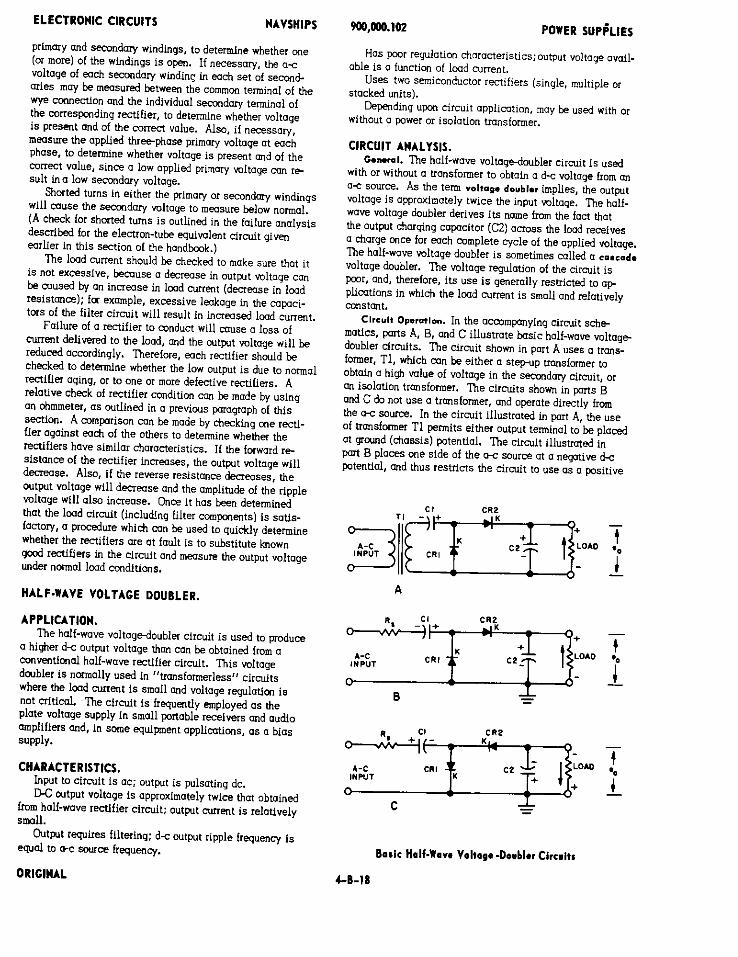
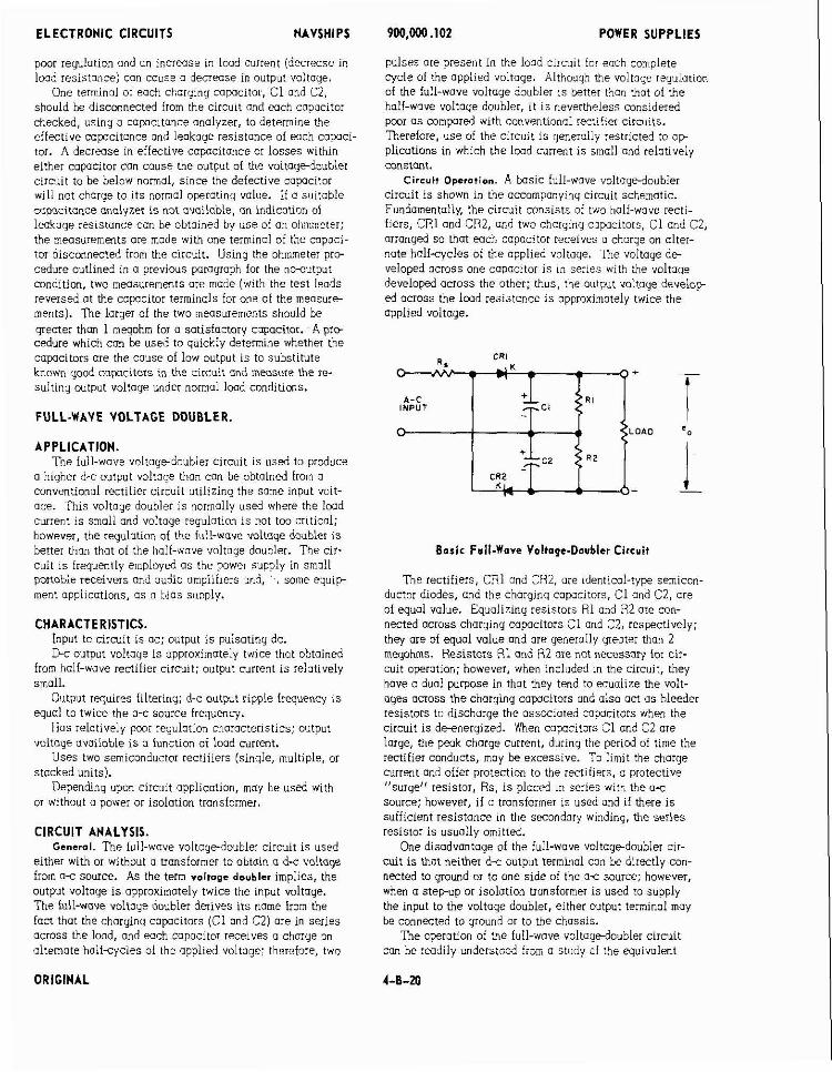
ELECTRONIC CIRCUITS HAVSHIPS
poor regulation and on increase in load current (decrwse in load resistance) can cause a decrwse in output voltage.
One terminal of each chorginy capacitor, C l and C2, should k disconnected from the circuit and mch copocitor checked, using a capacitance analyzer, to determine the effective capacitance and leakage resistance of each capaci- tor. A decrease in effective capacitance or losses within either copocitor can cause the output of the voltarje&joubier circuit to be below normal, since the defective capacitor will not charge to its normol operatiny value. If o suitable cawcitance anolvzer is not avoiloble, on indication ol leakage resistance con be obtained by use of an ohnmeter: the measurements ore made with one terminal of the copaci- tor disconnected from the circuit. Using the ohmmeter pro- cedure outlined in a previous paromaph for the nwutput condition, two measurements are made (with the test leods reversed at the capacitor terminals for one of the measure- ments). The larger of the two measurements should k qreater thm 1 meqohm for a satisfactoiy capacitor. A p r o cedure which con be used to quick!y determine whelner the capacitors are the cause of low output is to substitute known qood capacitors in the circuit and measure the re- sulting output voltage under normal load conditions.
FULL-WAVE VOLTAGE DOUBLER.
APPLICATION. Tqe full-wove voltoyrdoublei circuit is used to produce
o higher d-c output voltoge than can be obtained from a conventional rectifier circuit utilizing the some input volt- otre. This voltoge doubler i s normally used where the lwd current is smoll and voltoge rsyulotian i s not too critical; however, the rqulation of the full-wave voltaye doubler i s better than that of the half-7iave voltoge doubler. The cir- cuit i s frequently employed a s the power supply in smoll portable receivns ond audio ompliilers cod, ' . some equip- ment appllcotions, a s a !,!as sooply.
CHARACTERISTICS. Input to circuit i s oc: output i s pulsatinu dc, 6 z output voltage i s app;oximately twice that obtained
from holf-wave rectifier circuit: output current i s relotively smoll.
Output requires filtering; d-c output ripple frequency i s equal to twice the a-c source frequenq.
Hos relatively pwi reoulotion chorocter:stics: output . . voltoge available i s o function of load current.
Uses two semiconductor rectifiers (sinqle, multiple, or stacked units).
Depending upon circuit application, may be used with or without a power or isolotion transformer.
CIRCUIT ANALYSIS. Gcnsrol. The full-wove voltagedouble: circuit is used
either with or without o transformer to obtain a d-c voltage from o c source. As the term voltage doubler implies, the output voltage i s approximately twice the input voltage. The full-wave voltoye doubler derives its name from the fact thot the charging capacitors (Cl and C2) are in s s j e s across the load, and wch capacitor receives o charge m alternote hall-cycles oi the appiied voltoge: therefore, two
900,000 .lo2 POWER SUPPLIES
pulses ore present in the load circuit for each complete cycle of the applied voltage. Although the voltoqe regulation of the full-wave voltage doubler is better than that of the holf-wave voltage doubler, it i s r.evertheless considered poor a s compared with conventional rectifier circuits. Therefore, use of the circuit i s yenerally restricted to ap- plications in which the load current i s smoll and relotively mnstant.
Circuit Operotion. A basic full-wave voltayedoubler circuit i s shown in the occompanyinq circuit schematic. Fundomentolly, the circuit consists of two half-wove recti- fiers, CR1 and CR2, and two charging capacitors, C1 and C2, orranyed so that wch capacitor receives o chorqe on alter- nate half-cycles of the applied voltoge. The voltage de- veloped ocross one capacitor i s in serles with the voltoge developed across the other; thus, the output voltage develop ed across the load resistonce i s approximately twice the applied voltage.
CRI
A-C INPUT
Boric Full-Wave Voltage-Dovbler Circuit
The rectifiers, CRl and C92, are identical-type semicon- ductor diodes, and the charging capacitors, C1 and C2, are of equal value. Equafizinq resistors Rl and R2 ore con- nected across charging capacitors C1 and C2, respectively; they are of equal value and are generally qeater than 2 meqohms. Resistors R1 ond R2 are not necessary for cir- cuit operotion; however, when included in the circuit, they have a duo1 putpose in thot they tend to equalize the volt- oyes across the charging capacitors and also oct a s bleeder resistors to discharge the ossocioted capacitors when the circuit i s de-energized. '%en capacitors C1 and C2 are large, the peak charge current, during the period of time the rectifier conducts, may he excessive. To limit the charge current and offer protection to the rectifiers, a protective "surge" resistor, Rs, i s placed in series witt, the a-c source; however, if o transformer is used and if there i s sufficient resistance in the secondary winding, the series resistor is usuolly omitted.
One disodvantoge of the full-wave voltagedoubler cir- cuit i s that neither d-c output terminol can he directly con- nected to mound or to one side of the a-c source; however, when o stepup or isolation transformer is used to supply the input to the voltage doubler, either output terminal may be connected to ground or to the chassis.
The operation of the full-wave voltoyrdoublei circuit can be readily understood from o Sudy of the equivoient
ORIGINAL
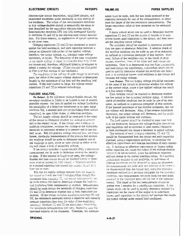
ELECTRONIC CIRCUITS
electron-tube circuit description. sim~lified circuits. and . . . associated waveforms given previously in this section oi the handbmk. The oction of the semiconductor rectifiers in this voltage-doubler circuit i s essentially the some os thot described for the equivalent electron-tube circuit. Semiconductor rectifier;^^^ ond CR2 correspond directly to rectifiers V1 and V2 in the electron-tube circuit descrip- tion. For h e s e r ~ s o n s , fin eiplanotinn of circuit operation i s not given here.
Charqiny copacitors C l ond CZ ore connected in series across the lwd resistance, and euch capacitor receives a charge on alternate h a l f q c l e s of the applied voltoge: therefoie, the output voltoqe, e,, contains some voltoge voriotions, or ripple. ?he frequency of the main cnmnanent
. . - :- "1 ,"r...;"p ,LO trmnlla,,-" "',hp V, L l ? s i,p),.r ." -y"-. ." . , . a-c source and, therefore, odditional filtering i s requlred to obtain o steady d c voltage. (Filler circuits are discussei in Port I3 of this section of the handbook.) - :ne ievAlution ,:,i th- v,?!:c,qc dxdhler c!rccit is relutively
p a r ; h e value Q! the output voltage obtained is determined largely by the resistance of the load and the resulting load current. If the load current i s large, the voltaye across capacitors C1 and C2 i s reduced accordingly.
FAILURE AtiALYSlS. NO output. In the f7ull-wave voltagedoubler circuit, the
nwutput condition i s likely to be limited to one 01 several possible couses: the lock of applied o-z voltoye (includinq the possibility of a defective transformer or on open surye ipsistors Rs) , a shorted load circuit (including filter circuit capacitor), or, open filter choke. ar defective rxti!iers.
The a-c supply voltoge should be measured ot the input of the circuit to determine wherier rile ru:ia~e is ~;?si:! and is the correct value. If h e circuit uses o ste.p;; :r isolatim tronsformet, measure the voltoge at the secondary terminals to determine whether it i s present ond i s the cor- rect vuiue. 'TP~UI the primary voIt0j.e :rmar& !!c!!! the tr,?!ii- former, continuity measurements of the primory and second- ary windinys should be mode to determine whether one oi the lin:inijj i; ;pen, s i x - a- cpe: circcit in either wind- ing wiil come a lack of secondsry ~l!o?e. .. me circuit incluJr- - - - 'Os\ " ..*,<,""ro a " a",,,= .c.,,aL". , ~ , ,, 4 ."-." measurement can be node !o determine wh-tiler t h ~ resistn! i s open. If the resistor i s found to te open, the voltoye- . .
doubler and load circuit i l u u i d be c:,ecke.' !;::he: !J ?e!?r- :.>?:.;. : :-"A JL!A,-:;\;~ ?=,- ti::=? ,I,.,r * .L . , ,L I *n"li*.ii __._ ..i., ;. : . ..~. ~ . . .
or o snorted copcltoi has cause; ;ilr r = A t ~ ; IG czt ZJ : !cse 14 !n "ps,
'',Withthe n-c sapzly ~ioltage remuv~j 1rn.i riie t,i@u; iu . i v ! wi!h the !md !incl::?ic:: fi!ter c!rc,~it! dis- connect& from ;??pu~ltu, 3:, rc;;st;;:e -2::;:::"::" ^?..
he .ade nrros.5 the 1md to determi:le whehei i:e lo;? 7::-
mi? (including filter comwnentsi is snortm. Mms,,rement* should be mode across the terminals of charging capacitors C1 and C2 to determine whether one or both copocltors ore shorted. (if h e circuii in;Iu&n eq~oliiiiig rz;i:to:z P! sc? 82, the resistance measured across o capacitor will norniaiiy measure somethinq less than tb.e val;e 3! h e ~ o l i z i n : ' !vs!sioi,) ,,.. "",, " .,. --"' -,." -2 .: ......, . .~ , ,,:,~,c:t~:s: , ,e>,.,<o,,~e : -- me - U O ~ . - , , , ~ , , . ~ tF ...., -,Ti> irnri, , , 6qv"ti irw, test-lwd polority of the ohmmeter. Therefore, two meosure-
POWER SUPPLIES
ments must be made, with the test leads reversed at the capacitor terminals for one of the measurements, to deter- mine the larger of the two resistonce measurements. The larger resistance value is then accepted a s t ~ e measured value.
A quick method which can be used to determine whether capacirors Cl md C2 are the source of trouble is to s u b stitute known gwd capacitors in the circuit, and Lien meus- ure the resulting output voltage.
The rectifiers should be checked to determine whether they ore open or otherwise defective. A relative chmk of the rectifier condition con be made by use oi on ohmmeter, os outlined in a previous parayroph a! this section. Hcw- ever, failure o! the rectifiers may be the result of other -C::E.S: !h?!o!!rp, t e c f ~ nf the filter ond load clrcult ore necessary. Once 11 is aetermined tnut Ciie iiitri ~ u l u p ~ o i ; . : ~
and iood circuit ore satisfacto~j, c procedure which cnn ke used to quickly determine whether the rectifiers are deiec- tivc i; 1s substitute k ~ w n good rectifiers in the clrcuit and meosure the output voitage.
LOW 0 ~ 1 ~ ~ 1 . The o-c supply voltoqe should be measured at the input of h e c i r c ~ i t to determine whether the voltage 1s the correct value, since o low applied voltoye can resuli in a low output voitoye.
Each rectifier should be checked to determine whether the low output is due to normal rectifier aqing. A relative check of rectifier condition con be made by use of an ohm- meter, os outlined in a previous porogroph of this section. If the forward resistance of the rectifier increases, the oul- put voltage will decrease. Also, if the reverse resistance iecreoses, the ou!put voitage wlii decrease, und tiir ampli- tude of the ripple voltoge will increose. - a ,r,zt,, ---. - L - . . ' J .,,,,.,. L a checked to make SIX? t h n t
it is not excessive, becailse the voltoge-doibie: circuit hi.s pmr regulation and an increase i n load current (decrease in load resistonce) can cause a decrease in output voltage.
One terminal of each charging capacitor, Cl ?n?. C?, should be disconnected from the circuit and each capacitor checked, us~nq a capacitance analyzer, lo determine the e!!ecfioe rnpcitnnce nnd ieakaqe resistance of each capoci- +-. .".. A decrease in effective copocitonce at losses within either copcitor can couse the output of !he voltarje-doubler rirc?ii! !c he below qormnl. since the defective copccitor will not charge to its normal operating value. if o sultabie ~jpasitance i;.;:i.zcr is no! .~3i!3h!~, miindirntinn n: :-L-..- ..>.vL7. .*.:.+..,-; ,. . -3. he -. ~ h : ~ : ~ " ? i;:. c; &Enc!~y:
i i e n ~ ~ s x e . h a > t s :rz . ~ z j c ;vi? ~2 : c : ~ : x ! c! !!- rm" -~- :ni disconnected fro^. the clr,cdit anl, usin? the lk~!r?Pt2r pmcedure ollti~ned i n ir p1evio.s pc;;~~op?, for me n?-oil%! ,-nniition. two xeosurenents ore mode (with the test leads i$v:rii.< i t 1% ?:~citc: tnr-i?l!4 !gi m i tne rnwstlle
ments). The lorqer of the tw3 memurenentc should k sieater than I meyonm lor u satisfoctuiy cupociior. i? 2r;- celure which can 'A #used to quickly determine wnelnri tile capacitors nie the couse of low output i s to substilute .:,,,,, y,, - - A ,,,,,,,.., :a,.... i.. ... .in ..,- ri.n,it -..-... nn _.d menailre the resnlt-
inq o7~tput voltage under normal load conditions.
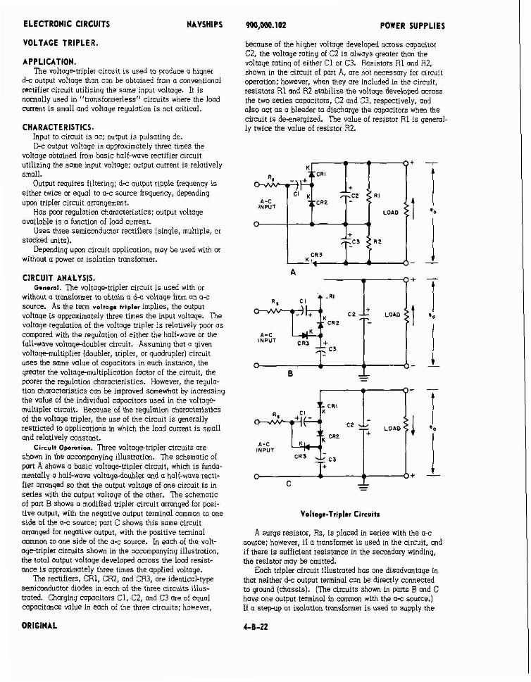
ELECTRONIC CIRCUITS NAYSHIPS
VOLTAGE TRIPLER.
APPLICATION. Tne voltaye-triplet circuit i s used to produce a higher
d-c output voltage than con be obtained from a conventional rectifier circuit utilizing the some input voltoye. It i s normally used in "transformerless" circuits where the lwd current is small and voltage reyulation i s not critiml.
CHARACTERISTICS. Input to circuit i s ac: output i s pulsating dc. PC output mltage is approximately three times the
voltoge obtained from basic half-wave rectifier circuit utilizing the some input voltage: output current is relatively small.
Output requires filtering; d-c output ripple frequenq i s either twice or equal to a-c source frequency, depending uw tripier circuit arrangement.
Has pmr regulation characteristics; output voltage available i s a function of load current.
Uses three semiconductor rectifiers (single, multiple, or stacked units).
Depending upon circuit application, may ke used with or without a power or isolation transformer.
CIRCUIT ANALYSIS. G.ner.1. The voltoge-triplet circuit i s used with or
without a transfwmer to obtain a d-c voltoge from on a% source. As the term voltage tr1~1.r implies, the output voltage i s approximotely three times the input voltage. I h e voltaue zeaulation of the voltaue t r i~ler i s relativelv Door a s . * - . . . compared with the regulation of either the holf-wove or the full-wave voltaae-doubler circuit. Assuminu that o aiven voltage-multiplier (doubler, uipler, or quadrupler) circuit uses the same d u e of capacitors in each instance, the grater the voltagemultiplication factor of the circuit, the poorer the regulation characteristics. However, the regula- tion characteristics can be improved somewhat by increasing the value of the individual capocitors used in the voltoge- multipler circuit. Bemuse of the regulation characteristics of the voltage tripler, the use of the circuit i s generally restricted to applications in which the lood current i s small and relatively constant.
Circuit Operotion. Three voltogetripler circuits are shown in the accompanying illustration. The schematic of part A shows a basic voltage-tripler circuit, which is funda- mentally a half-wave valtryedouhler and a half-wave recti- fier arranged so that the output voltage of One circuit i s in series with the output voltaae of the other. The schematic of part B shows o modified Gipler circuit arranged for posi- tive output, with the neqative output terminal common to one side of the a s source; port C s h o w this same circuit arranged for neqative output, with the positive terminal mmmm to one side of the a c source. In each of the volt- age-triplet circuits shown in the ocmmpanying illustration, the total output voltage developed across the load resist- ance i s approximately three times the applied voltage.
The rectifiers, CR1, CR2, and CR3, are identicol-type semiconductor diodes in each of the three circuits illus- trated. Charginy capacitors C1, C2, and C3 are of equol capacitmce wlue in each of the three circuits: however,
9aO.oOO.102 POWER SUPPLIES
h o u s e of the hiqher voltage developed across capacitor C2, the voltage rating of C2 i s always greater tho" the voltage rating of either C1 or C3. Resistors R1 and R2, shown in the circuit of part A, ore not necessary for circuit operation; however, when they ore included in the circuit, resistors R1 and R2 stabilize the voltoye developed anoss the two series capacitors, C2 and C3, respectively, and also act a s a bleeder to discharge the mpocitors when the circuit i s de-energized. The value of resistor R1 is generol- Iv twice the value of resistor R2.
A-C lNPUT
C R 2
LOAD
C R 3
C R 2
A-C
0 - -
Voltoge-Tripler Circuits
A surge resistor, Rs, is placed in series with the a s source: however, if a tronsformer i s used in the circuit, and if there i s sufficient resistance in the secondary winding, the resistor may be omitted.
Each tripler circuit illustrored has m e disadvantage in thot neither d-c output terminal can be directly connected to ground (chassis). (Tne circuits shown in pans B and C hove one output terminal in common with the a s source.) If a step-up or isolatim transformer i s used lo supply the
ORIGINAL
ELECTRONIC CIRCUITS NAVSHIPS
input to a triple1 circuit, either output terminal may be mn- nected to yround or to the chassis.
?he operation of the tripler circuits can be readily understmd from a study of the equivalent electmn-tube circuit descri~tions oiven oreviouslv in this section of the handbwk. ?he action of t ie semi&nductor rectifiers in a trioler circuit i s essentially the some a s that described !or the qji.n!ent e!ectnn-tube circuit. Semiconductor recti- fiers CR1, CR2, and CR3 correspond directly to rectifiers Vl. V2, and V3 in the electron-tube circuit description. For these reasons, on explanation of circuit operotion i s not given here.
In the circuit shown in part A, charging capacitors C2 and C3 ore in series across the lood resistance, and each
. ----: - -La.-- A" !,",$-,"lot "( f h p L Y p C ' L U l ,rrsLrrr " b,.-.y.. -.. -, applied voltoge: a s o result, the output voltaye mntolns some ripple. In thls tripier circuit, the frequency of t h ~ main component of the ripple voltage i s equal to twice the ~:P;-?,L.; L.! !j:e L i - s,oiii,-e. 11 t i c ci: .i!s shown in parti El and C, charging cnpacitnr C2 receives a charge on alter- nate halfcycles only; thus, the output voltage of these two circuits contains o ripple voltage which has a frequenq equal to that of the a c source.
As stated previously, the reyulatim of a voitoye- triple1 circuit i s relatively pmr; therefore, the value of the output voltage obtained from the voltage tripler i s determined lorye ly by the resistance of the lood and the resulting load cur- rent. 7he output of each of the circuits illustrated requires filtering to ohtain a steady d-c voltoge. (Filter circuits are ?iac>rssed in Part D of this section of the handbook.)
FAILURE ANALYSIS. No Output. in b e voilageiriP:cr i;l;blt, :ke ;.o~o-t>~!
condition i s likely to be limited to one of several possible muses: the lock of applied a-c voltoqe (including the possibility of an open surge resistor, Rs, or a defective stepup or isolatiwi transfom,er), a shorted loo4 circuit (including filter circuit components), open charging capaci- tors ldependmt upon circuit confiqurotion), or defective . . rectifiers.
The a-c supply voltage shoul? be measured at the input ~ ~
to the circuit to determine whether LLle voltage i s present and i s h e correct wlue. !f the circuit uses a stepup or isolation transformer, measure the voltoye at the secondary terminals m dererminr wneti~er it is pies%,: 2-2 i s : ic co:~
.vaiue. I! i;Kca-:iy, :he ;i;-.27 .<?l!~~e ~r..,!? '. removed from the tronsiormei ond cmtiwuity :;?asii%.r.;t; sf !he primary n-qd secnndory r-indinas mode 13 2ete:mir.e whether ,one ot the wind!nqs 1s epen, since on open cilcuii : - ..s -'.i-. L.u>... .%'...r".< wi i ! ,:c,j+e ,7 !,Xk of senr .da~, vo!tcze.
> ~. fi :he ci;c"t~ k:L2Je3 2 s ~ r ~ ~ -zs:s:zr; 0s: z :?5<zt?-z
mssurexent con te made to de!emine wllether the resistor i s open. I' the res!~tar i s found to be open, Lqe voitoye tripler and the lmd (including filter) circuit should k checked futmer to determine whether excessive lwd nlr-
rent, o de iedve recriiier, u~ u sir~iii.: izpzcit;; ?,c: ;3-z-d the resistor to act a s o fuse and to open.
, . kith the 0-c supply volmye remove3 f-m the ou!put tn -, ;...:.i.i. :; -,.,,, ,*,; :.~-:~, mr i,ILu,, ,,,~. ".,.. ".- 12-d >.,,.."_...- ...... , sr,.iiit\ dis- ,lm?,h22? tion :he !ace :er.::al oi C e ~ l i i o r 3, ~esisi~inct.
measurements can be made across the load to determine
POWER SUPPLIES
whether the lood circuit (including filter components) i s shorted. Mmsursmmts should be made across the terminols of charging capacitors C2 and C3 in the tripler circuit shown in pon A, or across chaiqiny capacitor C2 in the tripler circuit of wn B or Dart C, to determine whether the no- output condition i s inused by shorted capacitors. The tripler circuit shown in port A includes resistors Rl and W ; therefore, the resistance vaiue measured across wpuci- tors C2 and C3 will normailv be somethinu less than the value of the associated bleeder resistor. Since ine charqing capacitors are electrolytic capacitors, the resistance meos- urements will vary, depending upon the test-lead polarity of the ohmmeter. Therefore, two measuremmts must be mode, with the test leads reversed at the mpacitor terminols inr one nf the measurements, to determine the larger of the two resistance measurements. Tne Larger ;esistm;e ..:!:e i s mer, accepted 0s the measur?d vniue Copar:%tor C! may be checked in a similar monner.
A quick method which con te used to determine whether an open capacitor i s the source of trouble is to substitute a known ymd mpacitor in the circuit for the suspected capacitor, and then measure the resultiny output voltoge.
' h e rectifiers should be checked to determine whether they are open or otherwise defective. A relative check of rectifier condition can be made by use of an ohmmeter, a s outlined in a previous parayroph of this section. However, failure of one or more rectifiers may he the result of other muses; therefore, tests of the filter and load circuit are necessary. Once it i s determined that the filter components and load circuit ore satisfactory, a procedure which m n be used ro quickly determine whether the rectiiie;~ are deiec- t i w i s to substitute known good rectifiers in the circuit and -~ssii:e !he cutput ~ro!t?ge.
Low Output. The a-c supply voltaye should be measured at the input of the circuit to determine whether the voltage i s the currect wlue, since o low applied voltaye can result in a low output voltage.
Each rectifier (CRI, CR2, und CR3) should be checked to determine whether the low output i s due to normal r e d - fier aying. A relative check of rectitier condition con be made by use of an ohmmeter, a s outlined in o previous pmagrlph of this section. If the forward resistance of the rectifier increases, the output voltoge will decrease. Also, if the reverse resistance decreases, the output voltage will &crease.
3 e !md mrrest shou!? h ch&ed tn make sure that it i s not excessive, k o x e t5e ~~ol t3g~rr ipi?r circuit hiis
w r rer~lotion nnd nn increase in iwd current jdenwse in lwd resistance: ca; cause o d e c t s s e in 07utput witage.
One terminal of each chargin" capacitor (Cl, CZ, and C3) s?c;!< k d i scanec td !mm the cirniit and mcl~ caoacitor checked, using a capacitance analyzer, to determine its eifective capacitance and leakage resistance. 4 decrease in effective capacitance or losses witinin the capacitor can cause the output of the voltage-tripler circuit to be M o w nozc!. sizce the ?e!-!!v? rn(ncitnr will not charue to i ts normal operating value. if a suitable capacitance onalyzer is not avoiloble, an indication oi leakage resislance can be abmined by use of an ohmmeter. First, disconnect one '--I -1 -'.L.. ^^"^ '.^. '* ". ,LO ?,,,.,i*. t" Lelrrruiur ur urc .ry.mr, ..-... r.- -. 2 -. ohmmeter proceaure OirIIrnea lor me i i ~ u u ~ p u ~ L W ~ J ~ ~ ~ Y I , ,
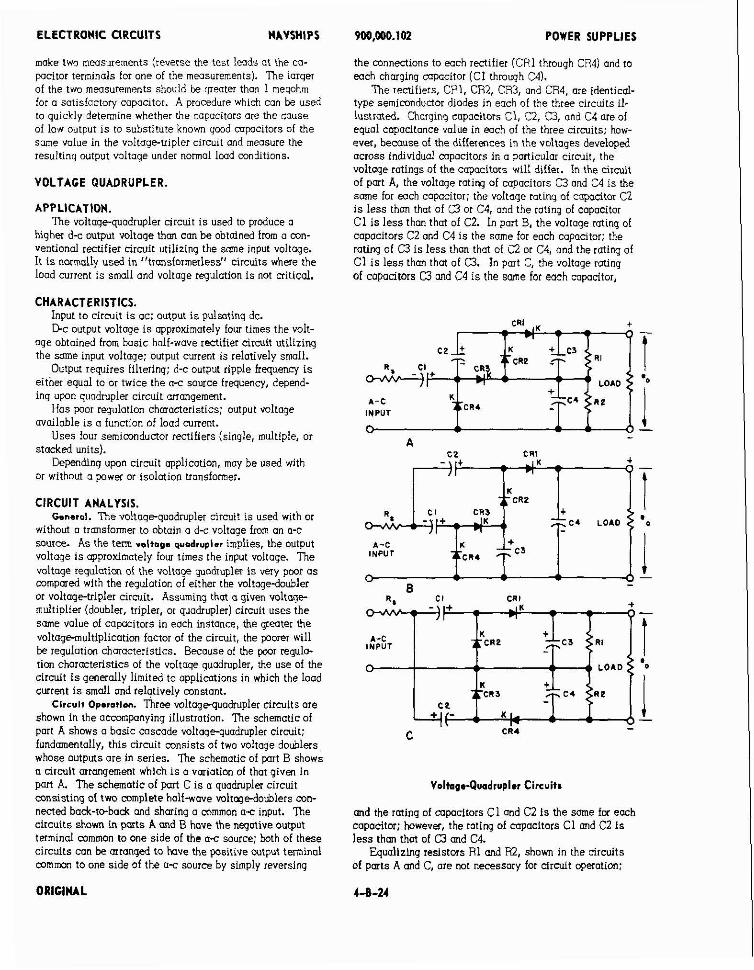
ELECTRONIC CIRCUITS NAVSHIPS
make two measurements (reverse the test leads ot the co- pocitor terminals for one of the measurements). ' h e larger of the two measurements shouid be greater thon 1 meyohrn for o satisfactory copacitor. A procedure which can be used to quickly determine whether the copacitors are the cause of low output i s to substitute known good capacitors of the same volue in the voitage-tripler circuit and measure the resulting output voltage under normal lwd conditions.
VOLTAGE QUADRUPLER.
APPLICATION. The voltage-quadrupler circuit i s used to produce a
higher d c output voltaqe than can be obtained from a con- ventional rectifier circuit utilizing the same input voltage. It i s normally used in "transformerless" circuits where the load current i s small and voltage regulation i s not critical.
CHARACTERISTICS. Input to circuit i s ac: output i s pulsating dc. D c output voltage i s approximately four times the volt-
age obtained from basic holf-wwe rectifier circuit utilizing the same input voltage: output current is relatively small.
Output requires filtering; d-c output ripple frequency i s either equal to or twice the o-c source frequency, depend- ing upon quadrupler circuit arrangement.
Has poor regulation chmacteristics; output voltage available i s a function of load current.
Uses four semiconductor rectifiers (single, multiple, or stacked units).
Depending upon circuit application, may be used with or without a power or isolation transformer.
CIRCUIT ANALYSIS. Gsneroi. The voltogequadrupler circuit is used with or
without a transformer to obtain a d-c voltage from an o-c source. As the term roltog. ~,ued.upl.r implies, the output voltage i s approximately fow times the input voltage. The voltage regulation of the voltage guadrupler i s very pwr a s compared with the regulation of either the voltagedoubler or voltage-tripler circuit. Assuming that a given voltage- multiplier (doubler, tripler, or quodrupler) circuit uses the same value of copacitors in eoch instance, the greater the voltage-multiplication factor of the circuit, the poorer will be regulation characteristics. Because of the poor regula- tion characteristics of the voltage guadrupler, the use of the circuit i s generally limited to applications in which the load current i s small and relatively constant.
Clrsvll Op.rotla. Three voltagequadrupler Circuits are shown in the accompanying illustration. 'The schematic of part A shows a basic cascade voltage-quadrupler circuit: fundamentally, this circuit consists of two voltage doublers whose outputs are in series. P ie schematic of part B shows o circult mrwement which 1s a vmiotion ol that aiven in
nened badr-to-back &d sharing a common be input. The circuits shorn in parts A and B have the negative output terminal common to one side of the a c source; hoth of these circuits can be mranqed to hove the positive wtput t m i n o l common to one side of the a c source by simply reversing
ORIGINAL
900,~0.102 POWER SUPPLIES
the connections to each rectifier (CR1 through CR4) and to each charging capacitor (C1 through C4).
' h e rectifiers, CRi, CR2, CR3, and CR4, are identical- type semiconductor diodes in each of the three circuits il- lustrated. Charging copacitors C!, C2, C3, and C4 are of equal capacitance volue in each of the three circuits: how- ever, because of the differences in the voltages developed across individual mpocitors in a particular circuit, the voltage ratings of the capacitors will differ. In the cirmit of part A, the voltage rating of capacitors C3 and C4 i s the same for mch capocitor; the voltage rotinq of capacitor C2 i s less than thot of C3 or C4, and the roting of capacitor C1 i s less than that of C2. In port B, the voltage rating of capacitors C2 and C4 i s the same for each capacitor; the rating of Q i s less thon that of C2 or C4, and the rotinq of C1 i s less than that of C3. In part C, the voltage rating of capacitors C3 ond C4 i s the some for each copacitor,
LOAD
A-C C R 4
INPUT
A - ;~n~~ C 4 LOAD o
A-C + INPUT C R 4
C 3 I - D -
w
A-C INPUT -
pon A. The schematic of part C i s a quadrupler circuit consistinq of two complete hali-wave wltme-doublers con-
Volbpe-Quadrupler Circuits
and the rating of copacitors C i and C2 i s the same far each capacitor; however, the roting of capacitors C1 and C2 i s less thon thot of Q and C4.
Equalizing resistors R1 and R2, shown in the circuits of parts A and C, are not necessary for drcuit operation:
ELECTRONIC CIRCUITS NAVSHIPS
however, when they are included in the circuit, resistors R1 and R2 equalize the voltages developed across capaci- tors C3 and C4, respectively, and also a n a s a bleeder to discharge the capacitors when the circuit i s de-energized. A surge resistor, Rs, i s placed in series with the a-c Source to limit the peak current in the rectifier circuit.
One &j;:i.;n:csc m~.m3:. to a!! three q~nd~i~p le r cir- cuits iiiustrmed i s that neither d-c output teiiri~o! CM be directly connected to ground or to the chassis: however, when a step-up or isolation transformer'is used to supply the input to m y one of these quodrupler circuits, either out- put terminal may be connected to ground or to the chassis. Furthermore, if a transformer i s used ond if there i s suf- ficient resistance in the secondary winding, the surge r e sistor, ?:, msy !!b omitted.
The operation of these quodrupler circuits con be readily understood from a study of equivolent electron-tube circuit descriptions given previously in this section of the handbook. Tne action of the sei~~icondue:oi recrifiers in tne quadrupiei circuit i s essentially tb,e s m e cs that d e scribed for the equivolent electron-tube circuit. For these reasons, an explanation of circuit operation i s not given here.
In the circuit shown in part A, chmging capacitors C3 and C4 are in series across the load resistance, and each capacitor simultaneously receives a charge, once for each complete cycle of the applied voltage; 0s a result, the output ripple voltoge has a frequency which i s equal to the frequency of the a-c source. In part B, charging capacitor ,. . . " ' .L .L- I-.' --A". -..-.. ;" rhnr",,li "" j; ;a pmuiiii ilii:: :::s L L ,.lu icr.r,",.r- ." " "... ...., ..~ alternate haif-cycles oi the applied a-c voltoge; therefore, the frequencv of the ripple voltage i s the same us the ire- quency of the a-c source. In part z, charging capacitors 3 and G1 m t in series across the load resistance, and the capacitors receive o charge on alternate hdf-cycles of the applied voltoge: a s a result, the output ripple voltage for this circdit has o frequenq which i s equal to twice the frequency of the o f source.
Since all three circuits described contain 4 rippie volt- age, odditionol fiitering i s required to obtain a sreody d-c voitoqe. {Filter circuits me discussed in Pan G of this section of the handbook.)
As stated previol;sly, she reguiutioi! of h e voltoge juad- ruoler i s relatively poor: the value of the output voltage ohtoined i s determined lorqely by the resistance oi the ioaci ooii the iesuitina liad ;;;rent. I: t?e ioai cxrrn! r.- large, ine output voltage is ri?u:ed acmrdiqly.
FAILURE ANALYSIS. NO Output. ;n riic vo;;~~i- ,~l i2r~&ei r,i;,l:, t k e : ~
output condition is l ikeb to be iimited to one 01 severd possfble causes- ihe l r ~ d i;f wp!ie? c s .ym!taqe (inc!s.'inq . ,be rur,,i,, L;!:.,, ...., -. ,.: mn ".. -,, -,en s u q e iesiztir. ?sj or 3 .'e!ective
step-up or isolation transformer), a shorted load circuit (in- cluding filter circuit components), open chaqinq mpaci- tors (dependent uwn circti! confiq~rntion) or defective iec- tiiiers.
The failwe ar.i!;sis p:oceauser !or the nwutput con- "h,nn, sot" us vuiiuuc irf i i iesist;;ce xeasureme?.:c,
' ~~ , .,.,: .. -*%-I.. -..LC ..,,,, ;*- ,,: n,,wm ,,,*, 4 "Y*ui..,. "... . . par,$ fir ;;;;zCc? p"!:, ztc. %_ra ersen!inliy t h ~ same SS
WO,OM).lOZ POWER SUPPLIES
those given for the voltaget~ipler and half-wave voltoge doubler circuits desnibed previously in this section of the handbook. Thsefore, these procedures ore not repeated here.
Low Output. The failure analysis procedures for the lowdutput condition mnsist of voltage, resistance, ond load-current measurements; capacitor and rectifier c h s k s ; substi!uti"n of known good parts for suspected parts: etc. These procedures me essentially the same as the procedures given for the voltage-tripler circuit desciibed previously, ond are somewhat similar to those given for the half-wove voltagedoubler circuit desnibed earlier in this section of the handbook.
Y!CY;\(OLThC-E !CDT! SUPPLY, SQUARE-WAVE OSCIL- LATOR TYPE.
APPLICATION. 7 3 , ;q:o:ewa,:? nsdl!n!nr type hi+-vo!toqe supply i s
a drto-dc mnverter used in electronic equipment for o p plicatians requiring extremely high-voltage dc at a small load current. The output circuit can be orranged to furnish negative or positive high valtoge to the load. The suppiy i s commonly used to provide high voltoge for accelerating and final anodes, ultor, and other similar electrodes of cathoderay tubes used in indicators.
CHARACTERISTICS. Uses two power tronsistors in a self-excited oscillator
circuit combined with a full-wave voltagedoubler circuit. Typical operating frequenq 1s between 4 w an6 iW
cycles. Cutput is high-vo1to;lr k ;: !--r. c-n-3. Regulation is ioir; m q be impcaved by re~ilating the
input d c supply voltoge. Rectifier circuit con be orranged to provide either posi-
t i v e or negativepolarity output voltage.
CIRCUIT ANALYSIS. Canard. ?h.e ~ q u m e v ~ e "scillator twe high-voltaae
supply includes a selfkxcited oscillator which has on operaling frequency in the range between 40(, m? ?KO cy- cles. R e osci!latoi circuit operates most efficiently os a squarewove generotor with the tronsistors iunctioninq as nigh-sped suriichuig e:emen:s. >.e t.z?.eis!crr 7 ~ v i r i e n
$i:z .:st&.le, z: f:ee?;r>r:i5;: 3~!ti.~k,ro!or ?irc:;!t; !kc acuon con be compoird to tiic ~ n i t c i ~ i n ; xti;: ..vilcl. 2:-
curs with o mechcnical vibrator in o nonsynchronous vibrg- tor supply. n e power supply (oscillatoi on: reiti!ier ;i:- ,:;1!5) is !ifn,i-ntlv ca!led a dc-to-dc converter. ~ n d the 3sc:!iatai ;ircui! ilsz!! i i ?c?-rrsJ :c 2 - 3 intnrob!c.cmrs
.quore way. oscillator. The squori-wcve output horn :he 0sci:lator circuit may be stepped up or down und redi:id to provide il d-c voltage bijter or lower than t i p inpiit volt- age. The circuit described here i s us& in mnjunctisn . . . ,. wirn o iml-wuve wli~~edi-L!e: citrd! !c cbt-i- '..i:h-,!~!!- nqe dc. Becouse of the squarewave output and the relo- tively high hequency of oscillation, very !!!tie filtering 1s
: e ~ ~ : : c . ' :o elimiz-te !he ripple unlt-qe from :he outwt: "i- ,,,,a .- ." b*pec.".., ."';., T?,,. ..-- ",hW " ieiz:ier ;ir;ji: i; used.
4-8-25
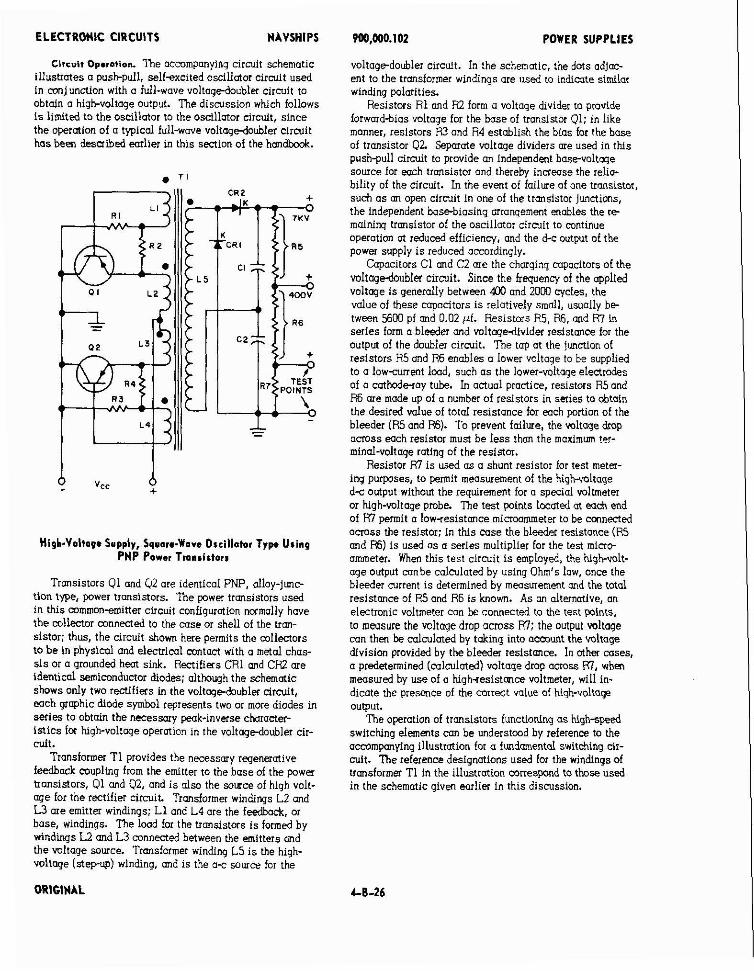
ELECTRONIC CIRCUITS NAYSHIPS
Circuit 0p.r.tion. Tne accompanying circuit schematic illustrates a pushpull, self-xcited oscillator circuit used in conjunction with a full-wave voltagedoubler circuit to obtain a highvoltage ou!put. The discussion which follows i s limited to the oscillator to the oscillator circuit, since the operation of a typical full-wave volmg&ubler circuit has been desaibed emlier in this section of the handbook. :Io 4 0 0 V
C2
TEST R7 POINTS
- - -
High.Voltage Supply, Square-Wars OsrillotDr Type Using PNP Power Tmnristorr
Transistors Ql and 02 are identical PNP, alloy-junc tion type, power transistors. R e power transistors used in this mmmon-emitter circuit mnfiguration normally h w e the collector mnnected to the case or shell of the tran- sistor; thus, the circuit shorn here permits the mllectors to be in physical and electrical contact with a metal chas- sis or a grounded heat sink. Rectifiers CR1 and CFI2 are identical semiconductor diodes; although the schematic shows only two rectifiers in the voltagedoubler circuit, each graphic diode symbol represents two or more diodes in series to obtain the necessary peak-inverse chamner- lslics fa high-voltage operation in the voltagedoubler cir- cuit.
Transformer T1 provides the necessary regenerative feedback coupling from the emitter to the base of the power transistors, 01 and 92, and is d m the source of high volt- age for the rectifier circuit Transformer windings L2 and U are emitter windings; L1 and L4 are the feedback, or base, windings. The load for the transistors i s formed by windings L2 and L3 connected between the emitters md the voltage source. Transformer winding L5 is the high- voltage (stepup) wlnding, and is the a-c source for the
900,000.102 POWER SUPPLIES
voltagedoubler circuit. In the schematic, the dots adjoo ent to the transformer windings are used to indimte similar winding palarities.
Resistors R1 and R2 form o voltage divider to provide forward-bias voltage for the bose of transistor Ql; in like manner, resistors R3 and R4 establish the bias for the base of transistor Q2 Separate voltage dividers are used in this push-pull circuit to provide an independent basevolteqe source for each transistor and thereby increase the relia- bility of the circuit. In the event of failure of one transistor, such a s an open circuit in one of the transistor j~unctions, the independent base-biasing arrangement enables the r e maining transistor of the oscillator circuit to mntinue operation at reduced efficienq, and the d-c output of the power supply i s reduced accordingly.
Capacitors C1 and C2 are the charging capacitors of the voltqedoubler circuit. Since the ftequenq of the applied voltage i s generally between 4W and 2000 cycles, the value of these capacitors i s relatively small, usually b e tween 5600 pf and 0.02 pf. Resistors R5, R6, and R7 in series form a bleeder and voltagedivider resistance for the output of the doubler circuit. The tap at the junction of resistors R5 and R6 enables o lower voltage to be supplied to a lowarrent lmd, such a s the lower-voltage electrodes of a c a t h o d ~ a y tube. In aciuol practice, resistors R5 and R6 are made up of a number of resistors in series to obtain the desired value of total resistance for each portion of the bleeder (R5 and R6). To prevent failure, the voltage drop across each resistor must be less than the maximun !er- minal-voltage rating of the resistor.
Resistor R7 i s used a s a shunt resistor for test meter- ing purposes, to permit measurement of the high-voltage d-c output without the requirement for a special voltmeter or high-voltage probe. The test points located at each end of R7 permit a low-resistance micrwmmeter to be connected across the resistor; in this case the bleeder resistance (R5 and R6) i s used a s a series multiplier for the test micro- ammeter. When this test circuit is employed, the high-volt- age output mnbe calculated by using Ohm's law, once the bleeder current i s determined by measurement and the total resistance of RS and R6 i s known. As an alternative, an electronic voltmeter con be connected to the test points, to measure the voltaqe drop across R7: the output ~ l t a g e can then be c a l ~ l o t e d by t k i n g into a m u n t the voltage division provided by the bleeder resistance. In other cases, a predetermined (calculatedl voltage drop across R7, when measured by use of a high-resistance voltmeter, will in- dicate the presmce of the correct value of hiqh-voltage output.
The operation of transistors functioning a s high-speed switching elements can be understood by reference to the accompanying illustration for a fundmental switching cir- cuit. The reference designations used for the windings of transformer TI in the illustration correspond to those used in the schematic given m l i e r in this discussion.
ORIGINAL
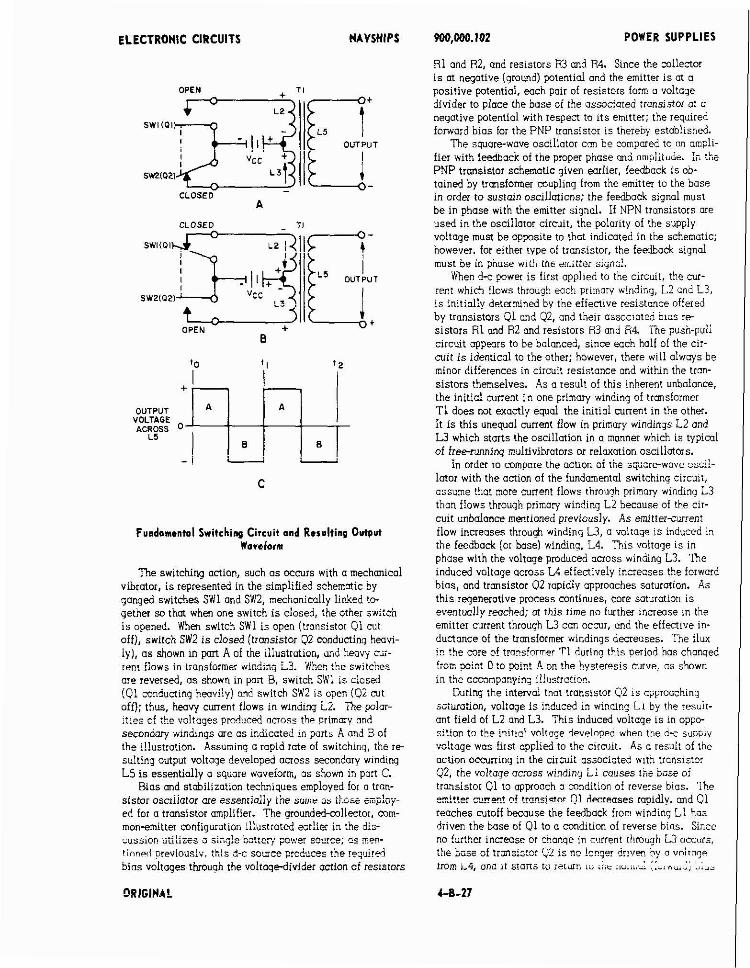
ELECTRONIC CIRCUITS NAVSHIPS
OPEN TI
OUTPUT
L3
- CLOSED
A
CLOSED
SWItPI
sWZla2)
OPEN + 0
Fundamental Switching Circuit and Resulting Output Woveform
The switching action, such os occurs with a mechanical vibrator, i s represented in the simplified schematic >y sanoed switches SW1 and SW2, mechanically linked tc- . . gether so that when one switch i s closed, the other switch i s opened. When switch SWI i s open (transistor 01 cut off), switch SW2 i s closed (transistor 02 conducting heavi- iy), as shown in pan A of the iilustration, and heavy air- rent fiows in transformer windinj L3. When the switches are reversed, a s shown in pan B, switch SW1 i s closed (01 mn?ucting heavily) and switch SW2 is open (02 ~t off); thus, heavy current flows in wlnd~ng Li. ?he polar- ties a i the voltages prodwed across the primmv ond secondary windlnqs me a s indicated in pans A and B of the illustration. Assuming o rapid rate of switching, the re- sulting output voltage developed across secondary winding LS i s essentially a square waveform, as shown in part C.
Bias md stabilization techniques employed for a tran- sistor oscriiator are essenriaiiy ihe suir ua i:ri.si- i-zp!rf- ed for a transistor amplifier. The grounded-collector, mm- mon-emitter configuration illustrated earlier in the d i e c"S>ioi . i s : - - - - -:-.I L-.t--. "- ,.,O. Fn.,,"e. "E ",en- U L ~ U L C ~ " rrllijre .," ..L.l rr..r. "- -.... .. ..... ~
tioned prer.iouslv, this d-c source ~roduces the required bios voltages through the voltagedivider acfion of reslsrors
Poo,ooO.lOZ POWER SUPPLIES
Rl and R2, and resistors R3 and R4. Since the collector i s at negative (ground) potential ond the emitter i s at a positive potential, each pair of resistors form a voltage divider to place the bose of the assoc~ated transistor at a negative potential with respect to i ts emitter; the required forward bias for the PNP trnnsistor !s thereby estohlished.
The square-wave oscillator can he compared to an ompli- fier with feedback of the proper phase and on~pliludi.. :n :he PNP transistor schematic qiven earlier, feedbock i s ob- tained by transformer mupiing from the emitter to the bose in order to sustain oscillations: the feedback signal must be in phase with the emitter signal. If NPN transistors are used in the oscillator circuit, the polarity of the supply voltage must be opposite to that indicated in the schematic; however, for either type of transistor, the feedback signal must be in piiose with the enitter siqn;!.
When d-c power is first applied to the circuit, the N-
wnt which flows through each primary winding. L2 and L?. is initially detamined by the effective resistance offered by transistors 0 1 and 92, and their associated 61cs r e sistors R1 and R2 and resistors R3 and R4. m e pusn-puii circuit appears to be balanced, since each half of the cir- it i s identical to the other; however, there will always be minor differences in circuit resistance and within the tron- sistors themselves. As a result of this inherent unbalance, the initial cunent in one primary winding of transformer T1 does not exactly equal the initial current in the other. It i s this unequal cunent flow in primary windings L2 and U which starts the oscillotion in a manner which is typical of freerunning multivibrators or relaxation oscillatois.
in order to compore the action of (he sqdarewnur ., ~b-.. , ; !-
latar with the action of the fundamental switching circuit, cssume that more mrer.! flows through primary winding L3 than flows through primary winding L2 because of the cir- cuit unbalunm mentioned previously. As emitter-current flow increases throuqh winding L3, a voltage i s induced in the feedback (or base) win&ng. L4. %.is voltage i s in phase with the voltage produced ocross winding L3. The induced voltage across L4 effectively increases the forword bios, and transistor 0 2 rapidiy approaches saturation. As this regenerative process continues, core saturation i s eve.~t~uallv reached; at this time no further increase in the emitter current throuqh L3 can occur, and the effective in- ductonce of the trmsiormer windinus decreases. The flux i- the cure of transformer T1 during this period has chanqed !:om point O to point A. or. the hysteresis curve, os shown ir. the ocmmponying illustrot~on.
During the interval that transistor 0 2 is approaching saturation, vol:oge is induced in windm~ I 1 by the resuit- ant field of L2 and L3. This induced voltaqe i s in oppo- sition to t k initloi voltage develop~o when the d r sdppiv voltage was first applied to the circuit. A s o result of the action occuiring in the circuit associated w.::, uwsistor 42, the voitoge across winding i: causes t6e Base of transistor 0 1 to appoach a condition of reverse bias. Tne e-itte: cxer.! D! tr~"s!nnr Ql decreases rapidlv, and 01 reaches cutoff because the feedback from winding L l has driven the base of 0 1 to o condition of reverse bias. Since no further innease or chanqe in ccarent through L3 occrirs, 'L- L--- c +----&-*... 'n 4. nm " lrlc uuac 0. , .rLn*.". -- r r ... . ,. ., , . trom 1.4, ana i f srons to reiwn cti ;:.c iw;;..- ,.-. n ,,,,
4-6-27
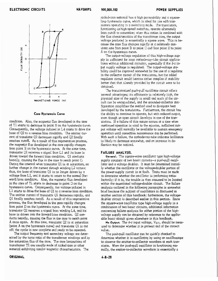
ELECTRONIC CIRCUITS NAVSHIPS
- o + MAGNETIZING FORCE IH I
Core Hyrtererir Curve
condition. Also, the magnetic flux developed in the mre of T I starts to decrease to point B on the hysteresis curve. Consequently, the voltage induced in L4 starts to drive the base of 02 to n reverse bias condition. The emitter cur- rent of transistor Q2 decreases rapidly and Q2 finally reaches cutoff. As a result of this regenerative process, the maqnetic flux developed in the core ra~idlv chanaes . . from piint B on the hystiresis curve. At the same t h e , transistor Q l receives a sianal from L1 ~d its base i s driven toward the forward Gas condition. Ql conducts heavily, causinq the flux in the core to reach point C. ~urin'the interval when transistor Q l i s at sotwotion, no further chanae in the current throuah windina L2 occurs: thus, the base of transistor Ql i s no lonqer Liven by a voltage from L1, and it starts to return to the normal (for- ward) bias condition. Also, the magnetic flux developed in the care of T1 starts to decrease to point Don the hysteresis c w e . Consequently, the voltage induced in L1 starts to drive the base of 0 1 to a reverse bias condition. The emitter current 01 tronsistoi Ql decreases rapidly, and Q l finally reaches cutoff. As a result of this regenerative process, the flux developed in the core rapidly changes from point Don the hysteresis curve. At the same time. transistor 02 receives a siqnoi from winding L4, and its base i s driven into the forward bias condition. 02 con- ducts heavily, causing the flux in the core to reach point A once again. At this time, transistor 02 i s at soturation (point A on the hysteresis curve) and transistor 0 1 i s cut off; the cycle i s now complete and rwdv to be repented.
The output frequency and secondary voltoqe are deter- mined by the turns ratio of the transformer windings and by the saturation flux of the cure. The core laminations of transformer T I are usually made of nickel-iron or other material exhibiting similar magnetic characteristics. n . e
ORIGINAL
9M),000.102 POWER SUPPLIES
nickel-iron material has a high permeability and o squore loop hysteresis curve, which i s ideal for use with trM- sistois operting in 3 switching mode. The transistors, functioning ashigh-speed switches, operote alternately from cutoff to saturation: when this anion i s combined with the flux characteristics of the transformer core, the output voltoqe produced i s essentiollv a square wove. This i s b e ~. ..glre r r t ccre !::x c..:r ]c; r:F1 i!:. -.I : :elatlvdl: coc- .Inn! rcte i:": poll1 1 lo p x n l :?: !rc- pc:r.: :. !c jo?rl A on the hysteresis curve.
The output-voltage regulation of this highvoltage s u p ply i s sufficient for most cathoderay-tube circuit opplico- tlons without additional circuitry, especially if the d-c in- put supply voltoge i s regulated. The output-voltage sta- bility could be improved somewhat by the use of a regulator in the collector circuit of the transistors, but the added requlator circuit muld become rather complex if stability better than thot olrmdv provided bv the circuit were to be . . obtained.
The transistorized push-pull oscillator circuit offers . . several advantages; i t s efficiency i s reiatively high, the physical size of the supply i s small and much of the cir- cuit con be encapsulated, and the grounded-collector con- figuration simplifies the method used to dissipate hmt developed by the transistors. Furthermore, the circuit has the ability to continue to operate, but with reduced output, even though on open circuit develops in one of the tian- sistors. If a failure of this nature occurs at a time when continued operation i s vital to the mission, sufficient out- put voltage will normally be available to sustain emerqency operation until corrective maintenance can be performed. With such a failure, the cothoderay-tube indicator brilliance i s likely to decreose somewhat, and an increase in de- flection may be noticed.
FAILURE ANALYSIS. General. Tne squarewave oscillator type high-voltage
s u o ~ l v consists of two basic circuits-o push-pull oscil- .. . . . lator and a voltoge doubler. It must be determined initial- ly whether the oscillator or the voltage-doubler portion of the power-supply circuit i s at fault. Tests must be made to determine whether the oscillator is performino s a t i s factorily; if it is, the trouble i s then assumed to be located within the associated voltaa~4oubler circuit. The failure analysis outlined in the following paragraphs i s samewhat brief because the sublen of oscillators i s discussed in another section of this handbook; furthermore, the voltage doubler circuit i s described wrlier in this section. Since the square-wave oscillator type high-voltage supply i s a combination of two basic circuits, additional information concerning failure analysis for either portion of the high- voltage supply can be obtained by reference to the applic able basic circuit given elsewhere in this handbook.
No Ovtput. ' h e d-c input voltage, Vcc, should be meas- ured to determine whether it i s present and of the correct value.
The push-pull oscillotor can be quickly checked to determine whether it i s oscillotinq by usina an oscilloscope - . to observe the emitter-toiollector waveform at each tran- sistor. When the push-pull oscillator i s functioning nor- mally, the emitter-to-milectar waveform is essentially a
ELECTRONIC CIRCUITS NAVSHIPS
squme wave having a peak-to-peak amplitude which i s a p proximately equol to twice the volue of the 3% input voltoge, Vcc.
Each biasinq resistor should be disconnected and, us- ing an ot~mmeter, the value of eoch resistor should be meos- ured to determine whether the resistor i s within tolerance. If the values of the blasinq iesistcrs (21 through P4) change opprrecinhiy: it i s likely thut the forwmd bias will change for the associated tronsistor; if the foiword bias in- creases, such a mnmtian may cause thermal runawcy, with eventual domqe to the transistor(s) and failure of the circuit to oscillate. Thus, with one transistor conducting heovily or with a shorted lunn~on within the transistor, the resulting current flow in the windings of transformer TI
.,"I --,.-- ---". ,h- -ff-,-+iv. -..-... . . > q i o ~ t - n p e . tn he ~ P , - T P C ~ P ~ ~ . t b . ~
core moy reach saturation, in whlch case the nrcuir wiii nor osciilore bemuse u! tile 1ua:inq sn the ;ir;;i: cau;e$ ty the defective transistor.
--...1-'-* '- ~."..-'..-.. Ti, EEcb .>B 5q"pnrn hnse "I ,.,,, " L ' L b ~ ',' ~, emitter winding, ar shoned turns in ony of the windings, will prevent the circuit from operating properly, since oscillations in each half ~f the circiit depend upor. regen- erative feedback from the transformer.
4 shoned secondary c:rcuit, reflected to the emitter and bse . # i - ~ - - ..,i..,s, m q cause excezsi'ic . i ~ u r ~ c lui~ich will pr- vent sustained oscillotlons. f i so , if :he b.igt:-vo!taqe winding, L5, should open, the circuit will continue to oscil- late; however, no output will be obtained hom winding L5 for the input to the voltagedoubler circuit.
If the oscillotor circuit i s found to be functioning nor- molly. then it must be cssumed that the mouble is in the voltagedoubler circuit or its associated load, and o check of ~ b ~ e rectilier ciscdit i f id; he ~ ~ 6 e i: zzcc:$z?z: !hc procedures outlined wrher in this section !G; the app11c- able rectifier circuit.
Low O~tput . The d r input voltage, Vcc, should be measure ;a de:e:mine ,whrrhe: ii i t af rice c n n x ; va!l;i.
If one tronsistor should develop an open circuit in one of i ts junctions, the hiqh-voltage output will decrease ifor : 3 % ~ !xi currsfit!, a!?? the penk-!"-?mk nmpiitode of the r i ~ p l e voltage will incrense. 3eco:ise of the independ- ent tlistbiasinq onaaqement, :kc rex3:~ing goo? tmnsistor wi!! csnti?~ie to cscillate. tinder 1 b . p ~ ~ conditions tile tronsformer core mcy not reach saturation. In this case there
i , ~ " ,&"*k,fi Lj, t:,s 2f:i:iczc; z! th,c :!:zi!, tcqe!b.e: . . -...- -- ...--"....."-..,;".- .l-.irr.i : E :hi , - , , , :~ , ; : ,;;':;;;- .. .... a,> --Lx...F.. ,.. , . ... . ~
. . runnermore, ine 0sci:k:c: !;equsxi nlil 1:.. .- -5; tr t:: i , r rnrpe times the ncim:l agc:atin;l !:icenc': nit.- o.!y 'me !rms!stor 1s opernrmg. A cal~bioirti usc~l;osmpe con be ~ s d tn ohserve the emittcr-tca!!c:!?: ~w~.:eform at each .!:::sist>!. :! ::.? c::;;;:t;: i: ?~:.z:;;::;: :z:-c!b.,, !% emitter-toallector waveform is easenlially a square wove hovinq o p d - t o - ~ e n k nrnpllfuoe wnlcn i s approxlmateiy e q ~ ! to twice the svn!ue of t i e is inpct voitoge, Ycc. Uowever, if only one transistor i s iunnioninq snd the other . . . , tr.,ns,srd, :,Lab 4 ) upe,t ci:cuit ir. cr,e zf its ;xz!ic?,s, :+e emitter-tocollector woveform will not resemble o square ,,we on La>, :;!ve: :! <:e zjc!?; i::td it wi!! :esemh!- o o--c:: X E ? io: O"'2 i!..l!<"Clr "T!? O tr.i;.ri i? fiii IF,? ".L". ..d<L-.,c:= ;= T'm:,,,"m:; ;!,*"L,,:,,:y, I! ," :rez:,*j,:y "~,,.. .. . . . ~ . ~ . .
900,0M).102 POWER SUPPLIES
of oscillation will be higher thon normal under these con- ditions.
If the oscillator circuit i s found to be operating normal- ly, 0 defect within the voltogedoubler circuit or associated load must be suspected a s the cause ot low output. For example, becotuse o! the relatively hiqh-impedance rectiiier and filter circuits, an excessive iocd current con c c s e t i t output voitoqe to be loir. tollure anciysls procedures typical rectifier circuits used in hiah-voltage supplles 3re outlined earlier in tbis section.
DC-TUDC CONVERTER
APPLICATION. -. ^P <c-1d.c cov.wter IVDICUI ~i t~ons:stiri iel ;C;JC:
suppiies used i n eircilurilc rquipnlcir; ;ui u$c!,L~;.;:.; :; ~ i - i ~ . . - l t - - ~ ir it mnAnmvo l nnA r l lrrpnf . 3- rill:- ,".."" ,",,'. ." ..-- "- ". - .--.
, , . px! circclt car be ,::1xgeq 13 ?~::z&:: !:ejcL~ve 5: p>:l:l'\:+ h i ~ h v r l t o g ~ to the inod. '?e supply is ccmmoniy use6 io prov~de hlgh voltoge for the opeidtior. oi sn.u:: iece:;tr: 3::
transmitters from o d-c power source.
CHARACTERISTICS. . $ uses two pov.ei t i ~ n s ~ s t o r s i; u sc!!-cxcitei csc!l!ztor
circuit combined with a bridge rectifier circuit. .,. lypical operating f r tq~ec? : z heweer (90 or? 4%:
cycles. Output high-voltage dc i s normally between 250 and
550 volts: load current i s between 60 cnd 200 milliamperes. Requlotion is good. Semlconducror diod~c -re used i!) ille r ~ i i i i e i ;irrl;ii. Rectifier circuit car be nnanaed to provide e~ther posi-
t;.;* ,?; "--"*<.."~""l",;+,, n, , ,n , , , >:mi,.,"m .lC~".,._ II__...l _..i_
CIRCUIT ANALYSIS. General. Tne d r t a d c converter is o spec~al opp!iio:ion
.I,! piv?r tr;;ii;:,~;; :c zo-..:c:: c !s;! ?-c ':?!!~?t. !? tini.- voltage dc. iicns~stor;zec power supplies ore frequently used in ploce of nlechunicui converters, S U C : as ,;h;~t;;: nnd dynnmotors. The circuit discussed here i s typic01 01
several types o! dc-tc-dc converters; the combination of o ysh-pu!! osci!!ator nn,? n br!,dne rpctriier r~s t~ i r s i ~ i 3 pui:.ei supply with ielativelu hiqh efficienw.
The osc~llotor circuit ltseii operotes most efficiently 0s - --..-.-... -..- -.-..-1-r !hl tm"<i<+nrq fi,nrlior,ipn " uy-". ., - . . ,-.. ". -.-. , ;; ~ i ~ i . ~ ~ ~ r I - L ~ - - atompntr . . . ....,.. ,..,... b.~. . ,~ . . .u . The csci!!~tor cLrr.~i! .. i> . .- x ,, ' 2stzL!e> =r ~cc~TL?::?~. -,:!!!,,!???!-- p,rp'!,T: -. t l e oction c2n be .ccmpa;e? t r the ~.#itc!!lnq -.ct?on :! ?
n~echanicd YiLrotsr iil i i r sc - j i i i~F , :~no~~ .2:3:3t2: SL;;!;.
The oscillator circuit i s freqoently r~feried to ns o imtur-
i t l e - < o r . * q " o r s ~ ~ * z v r ? C 3 ! ! ! l i " l ~
?,e 1i,?h-vo!tage 3-i oatput i:3m the gsci!!atnr !s reniilea ro provide a d r ourpui vn;ruqr, which f;:ic:c2. .A. !,:ll-wove recti!ier clrcglt is desirzbie in this t y x oi power supp!y to r edxr the filter cirmit reqiircxents: !c: tL:- ...La ------ .c"o",. ",," 1-1 L.."".."" ",.b"".,b ""1,. " ..., C. rin^l- .... -.- iiinh.\,nltn"a .. w?",,,""
i s requred, the bridge rectifier circuit is mmmonly empicy- e? .vit? !'.is p9w.r s,?pp!y. Sem!e~n.'~;nnr 113:~s CIP !.LC::
. . , 7< .. ra,-,.;!ie?< . - ~ ~~~~~~ in I>,$ b,:i2,72 c::zp.. 3ec:;ze 5: t:e cT;c:* Wt!"? <>88 :v \ i L",,, t!.e L36cil:atsr zz6 5cCGze :>,c :::cxz2; of oscliiat~an is relnrlvely nlgn, very ~ l t t ~ c i ~ i s i i i , : is ii-
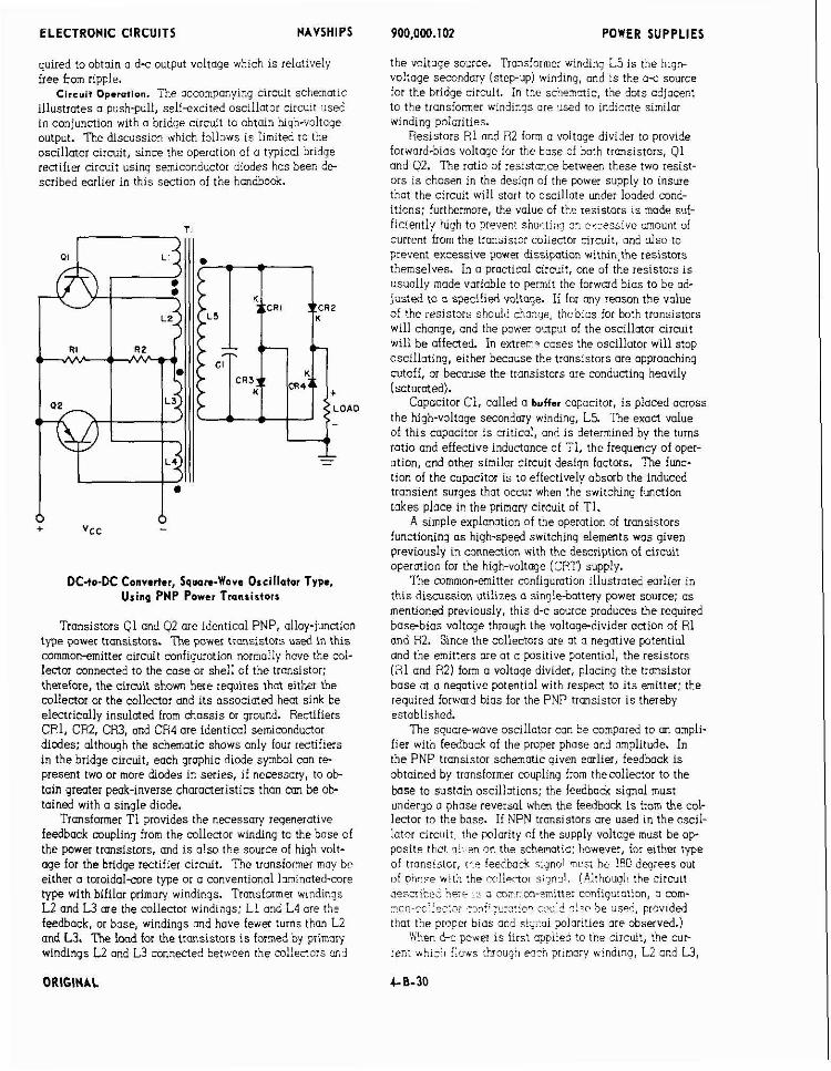
ELECTRONIC CIRCUITS NAVSHIPS
quired to obtain a d s output voltage which i s relatively free from ripple.
Circuit Operation. The accompanying circuit schemot~c illustrates o push-pull, self-excited oscillator circult used in conjunction with a bridge circuit to obtain high-voltage output. The discussion which follows i s limited to the oscillator circuit, since the operation of a typical bridge rectifier circuit using semiconductor diodes has been de- scribed earlier in this section of the handbock.
DC-to-DC Converter, Sqwn-Wove Orcillator Typo, Using PNP Power Transistors
Transistors Q l and 02 me identical PNP, alloy-junction type power transistors. Tne power transistors used in this common-emitter circuit configuration normally have the coi- lector connected to the case or shell of the transistor; therefore, the circuit shown here requires that either the collector or the collector and its associated heat sink be electrically insulated from chassis or ground. Rectifiers CR1, CR2, CR3, and CR4 are identical semiconductor diodes; although the schematic shows only four rectifiers in the bridge circuit, each graphic diode symbol con re- present two or more diodes in series, if necessary, to o b toin greater peak-inverse characteristics than om be o b tained with a single diode.
Transformer T1 provides the necessory regenerative feedback coupling from the mllector winding to the base of the power transistors, and i s a!so the source of high volt- age for the bridge rectifier circuit. The transformer may be either a toroidal-core t w e or a conventional laminated-core type with bifilar prima& windings. Transformer windings L2 and W are the collector windings: L1 and L4 are tL,e feedback, or base, windings and have fewer turns than L2 and L3. The ]load for the transistors i s formed by primary windings L2 and L3 connected between the col!eors md
ORIGINAL
9M).O00.102 POWER SUPPLIES
the voltoqe source. Transformer winding L5 i s the hign- voltage secondary (step-up) winding, ond i s the a-c source for the bridge circuit. In the schem"tic, the dots adjacent to the transformer windinqs are used to indicate similar winding polarities.
Resistors R l and R2 form o voltage divider to provide forword-bias voltage for the bose of both transistors, Q1 and 02. The ratio of resistance between these two resist- ors i s chosen in the design of the power supply to insure that the circuit will start to oscillate under loaded cond- itions; furthermore, the value of the resistors i s made suf- ficiently high to prevels shu,.ti>g c~ er:essive mount of current from the transistor coilectoi circuit, and also to prevent excessive power dissipation within.the resistors themselves. In o practical circuit, one of the resistors i s usually mode variable to permit the forward bias to be od- justed to a specified voltoqe. if for any reason the value of the resistors should chznge, thebios for both transistors will change, and the power output of the oscillator circuit will be affected. In e a r e r - coses the oscillator will stop oscillating, either because the tronsistors ore approaching cutoff, or because the transistors are conducting heavily (saturated).
Capacitor CI, called a bvHsr capacitor, i s placed across the high-voltage secondary winding, L 5 The exact value of this capacitor i s critical, and i s determined by the turns ratio and effective inductance of Ti, the frequency of oper- otion, ond other similar circuit design factors. The iunc- tion of the capacitor is to effectively absorb the induced transient surges that occur when the switching function takes place in the primary circuit ot TI.
A simple explanation of the operation of transistors functioning os high-speed switching elements was given previously in connection with the description of circuit operation for the hiqh-voltqe (CRT) supply.
The common-emitter configuration illustioted mrlier in this discussion utilizes a sinole-botterv cower source: os . . mentioned previously, this d-c source produces the required base-bios voltaae throuah the valtooedivider onion of R1 ond HZ. Since the collectors are at o negative potential and the emitters ore at o positive potential, the resistors ( R l and R2) form a voltage divider, plocing the transistor base at a negative potential with respect to i ts emitter: the required forwmd bias for the PNP transistor is thereby established.
The square-wave oscillator con be compared to an ampli- fier with feedback of the proper phose and amplitude. In the PNP transistor schematic given earlier, feedback i s obtained by transformer coupling from thecollector to the base to sustain oscillations; the feedback signal must underqo a phose reversal whm the feedback i s horn the col- lector to the base. If NPN tronsistors ore used in the oscil- lator circuit, the polarity of the supply voltage must be o p posite that n:.. sn nn the schematic: however, for elther type of transistor, 1i.e feetibad ,iIgnol ~ c s r hc 180 dqrees out of ohnse with the cell-rtor siqnnl, [Plthouqh the s i rn~ i t aesciicec her? 1: 3 mrron-emitter cc~l?iguiolion, o cnm- - , c::-rci.e::-; :;+~I::Z!~O" c'cI? ?!I? be use?, provlded
that the proper bias ond s!j::ai polarities are observed.) Cihen 6-c power i s first applied to the circuit, the cur-
reii; whiz5 f i s ~ s r b ~ o u j h ec-.il prlnory winding, L2 and W,
ELECTRONIC CIRCUITS NAVSHIPS
i s initially determined by the effective resistance offered by transigors Q1 and 92 ior a given value of base-bias voltage. The push-pull circuit appears to be balanced, since each half of the push-pull circuit i s identical to the other; however, there will alwoys be minor differences in circuit resistance and within the transistors themselves. As o resnlt of this inherent unbalance, the Initial current in one
_..al-. v.....,, . nrinding does net exoc!iy equal the current in the
other windinq; it i s this uneaual current flow in primarv windings ~ 2 k d L3 which s t h t s the oscillation^ Theim. mediate effect i s that one transistor conduns while the other i s cut off.
For the purpose of this explonotion, ossume tho1 more current flaws through winding L2 than flows through wind-
', - 5 +L.. . l : - i s iliffnrpnin in tho triln4isfnls: >:,q W "FvlUrc u. ..,. r..r.+. .~~ thus, transistor 0 1 altempts to conduct more hwvliy tnan does tronsi tor Q2 As che milector-current !:fin izcrmses through win ng L2, a voltage is induced in the iee4back , , % ' ;or ainding, 1.1. n; induced :.~ltzge in L! is !RO degrees out of phose with the voltoae oi L2, a s shown by the dots used on the schematic to indicate winding polar- ities for transformer T1. Tnus, an out*i-phase voltage i s applied to the base of transistor Ql, which drives the base more negative and causes Q l to increase conduction. 'While Ql iapidy approaches saturation, because of the increase in forward bias caused by the voltage from Ll , lhe voltage induced in feedback winding L4 by the resdtont field of L2 and W applies a positive signal to the base of truns- istor 02; thus, the base of Q2 is driven toward o condjtion nf reverse bias, transistor 02 opprwches cut off, and ml- !ectorc~rrest flow throljqh ,winding L3 decreases mpidiy.
?his regenerative process continues until transistor i;l 1s ot satwauon, translsrur C2 ia h i ;::, i : e xagne:ic flux deveiowd in the core reaches saturnion, and no iurther increase in'collectot current occurs in prima& winding L2. Since the current throuah L2 is at maximum and the eiiec- live inductance of the windings has decreased as the ccre reached flux saturation, no further voltage i s induce6 in windings Ll , W, and L4. The base of transistor Q i i s no Lonoer i j i .ve~ i,; a fedhack sic!!%! from I! md thus starts :o return to the normal (forumd) hios mndition established bv resisrors Rl and 82. %e fliia iz :L,- core srmts to d e a e a s e os the magfietic field &out the core starts to ml- lapse. ?his anion, in !urn, induces voltoges in the wind- lngs opposire io those which piavi;;s!y zxiste?. ?Fe h e
> ? ,..i.' ai .c^"i ...- r: rnr::i\ie ii;;;! i.-- ... ;.. ..:'.,,. ib.a.-. v i ; ,,. ...,.... ..: ~ ,,".. ..... d- Inn il? wrtlcn & ~ v e s tne hose into a ie ie isrbias i~di:i~: I? c.t ~ f i 01, Olw. the vcltaae induced in *inding L4 i s negeive, ad returns the base oi Q2 lo u forword-bias cand- i!io? !1 start rnn'lnrtion. As trcnsistor 02 starts to mn- i"3, ~::e.c:-.:~r:~nl ;la., :k.ia;,;?, ::ix:.y ..vi:e::: L3 !?-
nmses nnd induces o voltoqe in feedbock ivinding L4. As 3 result, the negative voltaqe lnduced in wind~ng i4 is iurcher increased; thus. !he h s e of L'2 is driven stiii further into the iorward'iias condition, which causes 02 to rapidly opproouii huilii~tiiii~. '!!hi;!i 02 c p p r c c c h ~ ~ SG!-
~ . ~. uration, the positive voltoqe induced in feedhack winding L i is oppLied m t:i bc32 C! !:azsis!or 121; !h~ls, the bas? . *. Sf y: ;, .:.:.x !o,A>zr:. K,n,ji!i,?n n! ;P;e:sp $3:. >az*s- I-. ,.., "I ,; -n-.r-.-ine uwu.-,u..~.. ri,rn;i z.1 rnl!n:iui~.utiei~t 23" :Lz;;;k. windinq L2 decreases rapidiy.
POWER SUPPLIES
?%is regenerative process continues until transistor Ql i s cut off, tronsistor 0 2 is ot saturation, the magnetic flux developed in the mre again reaches soturotion, and no further increase in collector current occurs in primary wind- ing L3. Since the current through L3 i s at maximum and the effective indunonce of the windings has decreased os the mre reached flux saturation, no further voltoge is induced in windings L i , ii, and i4. Tne base of irulrrisioi Q2 is no longer driven by o feedback signal from L4, and thus starts to return to the normol (forward) bias condition established by resistors R l and R2. The flux in the core once wain starts to d ~ r w s e a s the magnetic field about the mre starts to collapse. This anion, in turn, induces voltages in the windings opposite to those which previously ~ r i a t cd . The base of transistor 02 now receives a positive slgnai imm winding L4, rvk>ich ie!~;;.s f?.e Scse iztc 3 r e v = . s ~ b i o s condition to c3t off 02. Also, the voltage in- duced in winding L1 i s negative, and returns the base of Q l to 0 forword-bias condit~on to start conduction. As transistor 0 1 s t ~ s to mndun, coilectorzment flow through primary winding L2 increases and induces o wi r - oqe in feedback winding L1. As a result, the negative vo l tqe induced in winding L1 i s further increased: thus, the base of 01 i s driven still further into the iorword-bios mndition, which causes Ql to rapidly approach saturation. While Q l approaches saturotion, the positive voltage in- duced in feedback winding L4 is applied to the base of tran- sistor 02; thus, the base of 92 i s driven toward a mndition of reverse bias, transistor 02 approaches cutoff, and col- lectorcurrent flow through windinq L3 decreases rapidly. -. . i n l s regenerative process coa;iri;es iu z;::pl;';t ihe cycle: transistor 0 2 i s cut off, transistor Q i is at saturation, the - q l e t i c !!LY 6eve.iped din the core aoain reaches sat- uration, and no further increase in collector current occurs In primary winding L2. Since the current ihroujh L? i s 31 maxinun and the effective inducfance of :he windings hos decreased a s the core reached flux saturation, no further voltage i s induced in windings L1, L3, a d L4. n2 base of tronsistor 0 1 i s no longer driven by a feedback signal from L l , and thus starts to return to the normal (forwordj bias condition. ?his action completes the first cycle oi operation and another cvcle i s ~nitiated a s the flux in the core once aqain starts to decrease and the magnetic field a b u t the core starts 10 collapse.
From the discussion above it can be mncluded that !t3~.EiSlOIs C)! n ~ d Q2 f)unc!ion a s high-speed switches. -.. .,cralxq d t s ra t e iy imm cutoff tn sotomtion. Whni ttiia nultivihrota-tvoe ~ C ~ I O F . is combined with the flux churac- . . teristics of the !rzn.sformer core, toe output voitage pro- duced across the Noh-voltaae secondarv windinc, L5. i s *. . ~ . ~ . w r i a l l ~ o square WOYC. ; h e outpui m i r q e ~inp; . i~; ie and oscillator frequency ore determined by the tuns ratio ;i the primary m,e semn3a:y winnings 0.16 hy !ble sn!m~lutio~, liux ot the trarisformer core mc;eriai.
F41LUOE ANALYSIS. Gen.rol. 'The :c-to4c converter consists c! n push~cl!,
sqiare-wave osailntar and a brldgr rectifier circuit. !t .;i:at be deternined initidiy whether the osci1:atoi i i the ' "'ruqi- " - - - . : I : - . L C L Y L I C I * ..i ll"...",. ni -. t i n ...- ""We1 ?" s " ~ n i v is or io,,ir. . , . . . . .., , . ~ e s t s must oe moae to fieier;,;~i,c a;.e..mi i..i i2i;l.u.a. ...
ELECTRONIC CIRCUITS NAVSHIPS
peiform:ng sotisfoctorily; if it is, the trorble i s then as- s,med to be located within the brldge rectifier circuit (in- clu2ing fdter circuit components). The follure analysis outlined in the following parcgiapLls i s somechst brief be- x u s e t t e subject oi oscillators is discussed in another section of this handhook; furthermore, the bridge rectifier circuit using semiconductor diodes as rectifiers i s d e scribed emiier m this section. Since the dc-to-dc convert- er i s o combination of two basic circuits, odditional infor- motlon concerning failure analysis for either portion of the transistorized power supply ioscillator or bridqe rectifier) can be obtoined by reference to the applicable basic circuit qiven elsewhere in this handbook.
No Output. The d-c input voltage, Vcc, should be measured to determine whether it i s present and of the mr- rect value.
The push-pull oscillotor con be quickly checked to determine whether it i s oscillatinq by using an oscilloscope to observe the mllector-to-emitter waveform at each transis- tor. 'Wen the oscillotor i s functioning normally, the col- lector-to-emitter waveform is essentialiy a square wave havinq o peakto-peak amplitude which i s approximately ~qi131 to Mice the volue of the d-c input voltage, Vcc.
If the volue of either or both biasing resistors, R1 and E2, shollld chnnge appreciably, the forword bias on both transistors will change. If resistor Rl decreases or resist- or R2 increases, the forward bios on both transistors will decrease and cause less collector current to flow; converse iy, if resistor R1 increases or resistor R2 decreases, the forward bios on both transistors will increase and cause additional milector current to flow. A denmse in forviard bios causes both transistors to approach cutoff and to event- ually stop oscillations: on the other hand, on increase in forword bias causes both transistors to opprooch saturation 2nd !o eventually stop oscillations. This latter condition {increased forward bias) may muse thermal runaway, with subsequent damage to the tronsistors themseives. There- fore, the forward-bias voltage must be measured to dcter- !nine whether i t i s correct and within tolerance for the volt- uqe specified. If not, remove the input voltage, disconnect one end of each resistor, ond, using an ohmmeter, measure the volue ui euch resistor (R1 and R2) to determine whether the resistors are the correct value.
Any defect in transformer TI, such a s on open base or collector winding, or shorted turns in ony of the windiws, viill prevent the circuit from operating properly, since oscil- iations in each half of the circuit depend upon regenera:ive feedback from the transformer.
A shorted secondary circuit, reflected to the collector und bose windings, may couse excessive losses which will prevent sustained oscillations. Also, if the high-voltage winding, L5, should open, the circuit wiil continue to oscillate; however, no output will be obtoined from winding L5 for the input to the bridqe rectifier circuit.
A shoned junction in one of the tronsistors will cause excessive current to flow in the associated winding (L2 or L3) of transformer T1. This, in turn, will cause the effective is~.ductance of the tronsformer to denease, the mre may reach saturation, and, becouse of the loading on the circuit caused by the defective transistor, the circuit .will not ascii1.lt.e.
CRIGINAL
900,W0.102 POWER SUPPLIES
If the oscillator circuit i s found to be functioning nor- mally, then it must be ossumed that the trouble i s in the bridqe rectifier circuit or i ts ossocioted load, and o check oi the bridge rectifier must be mode in ocmrdonce with the procedures outlined earlier in this section for the avvlic- . . able rectifier ~'rcuit .
L o r Output. The d-c input voitoqe, \ice, should be measured to determine whether it i s of the correct volue.
If one transistor should develop on open circuit in one of its junctions, the remaining good trmsistor will continue to oscillate; however, the high-voltage output will d e crease (for o given load ~llirent), and the pwk-to-peak amplitude of the ripple voltage will increase. Under these conditions of operation the transformer care moy not reoct, saturation. In this case there will be a reduction in the efficiency of the circuit, together with an accompanying decrease in the output voltoge. Also the ascillatn ire quency will increase to two or three time the norm01 operat- ing irequency when only one transistor i s operating. A calibrated oscilloscope mn be used to observe the collect- oi-to-mitter waveform at each transistor. If the oscillator i s functioning normally, the collector-to-emitter waveform i s essentiaily a square wave hovinq a peak-to-peak ampli- tude wh~ch i s approximately equal to twice the volue of the d-c input voltage, Vcc However, if only one transistor i s functioning and the other transistor has on open circuit in one of i ts junctions, the collector-to-emitter waveform will not resemble a square wave on both halves of the cycle: instead, it will resemble a square wove for one half-cycle and o trapezoid for the other half-cycle. As mentioned p r e viously, the frequency of oscillation will be hiqherthan normal under these conditions.
In the common-emitter circuit configuration, a relatively small change in base current produces o relatively large change in collector current. Tnerefore, the farward-bios vo l tqe applied to the bose of the tronsistors i s imponant, since the voltage has a dired effect upon collector current ond upon the oscillaror power output. (Refer to the failere analysis discussion concerning bias resistors R l ond R2 given in o previous paragraph for the no-output condition.) Therefore, the forward-bias voltoqe should be measured to determine whether it i s correct ond within tolerance. If not, the volue of the bias resistors should be checked by use of the ohmmeter procedure outlined previously; if the power supply i s equipped with a voriable bios resistor, a bios adjustment moy be required.
I f the oscillator circuit i s found to be operating normally, a defect within the bridge rectifier circuit (including filter mmponents) or the associated lood circuit must be suspect- ed os the cause of low output. Far example, an excessive
load current can couse the output voltoqe to be low. Fail- lire analysis procedures for the bridge rectifier circuit using semiconductor diodes were given earlier in this section of
sthe hcmdbwk.
DOSIMETER CHARGER (DC-TO.DC CONVERTER).
APPLICATION. f i e dosimeter charger is one typical application of the
dc-tc-dc converter circuit. The dosimeter charger i s o sslf- mntained, portable, bottevdperoted, transistorized power
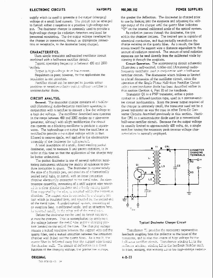
ELECTRONIC CIRCUITS NAVSHIPS
supply which i s used to generate o d-c output (charging) voltage at a small iood current. ;he circliit can oi anariyed to furnish elther a negative or o positive hijh-voltage out- put. The dosimeter charqer i s commonly used to provide a high-voltage charge for radiation detectors employed for personnel monitorinq. The d-c output vokaqe developed by the chmqer is transmitted, through or, cppropriate zonnec- tinri or rweptocle, to rhe dosimeter being i i ; u r ~ e d .
CHARACTERISTICS. Uses single trcnsistor self-excitec oscliiator clrcuit
combined with a half-wove rectifier circuit. 1- ,yplcal operatin7 i;equr.:cy ; s bet,iee; &I0 o:$ 2050
mcles. nl,tp,,+ b,3h-.l,~ltn30 .!P qt !PW ~ I T T P " ~ ~
Hequiotlon t s poor; however, tor tne appiicm~on the fedulation is no! itr~w~laiz;.
!'ecti!ier c i ra i t c::; be a:rmgeL ts Srovide e!!:er nnri,i,,-^. rannt i , .o . . - !" r i l , ",,.. ,I -wn'rn*o. ,*,. ~ i f i e , , - "-" -, ,-... . ...-... .~~ .. semiconductor diode.
CIRCUIT ANALYSIS. General. The dosimeter choigei consists ot c tickler-
coil (Armstrcnl) audlo-irewency osclilnor operatinil in conjunction with n rectifier to mnven a low d-c voltage to a hiqh d-c voltaqe. nihe oscillator descrioed fiere operates in the ronqe between 400 snd M O O cycies os a sinewave generotor, although with slight modification the circuit can operote as a blocking oscillotor to produce a s q u o i e wave. 7he hiqh-voltoqe a-c output from the oscillotor 1s
:pcti!ied to provide G ?-c octput :.0:t3;0 whih*, 1s the? filtered to remove ripple, and opplled to the electrosrrpe . . ,. ~. , .. -<.,einbiy ci the ?osimete: lo: :x~ ,x rne ' r~ : .
A brief dzsniptlon oi 5 s;i,zl!, $re;;-;a;&;.; suc i~t dosimeter, used to measure X and qommo rsdiotion, 1s :n order at this time so that the appllcotlon of the charger may be better -.derstood.
The pocket dosimeter is one of seve r i rodiotion mcfii- tonnq instruments utiiiz~ng the o~l i l ty oi radimlon to pro- dgce innizo!in" in y S e ~ . Th. do~ i rnp t r r j ? nnnrnrimnt~lv the size of a iciintoin pen, a n consjrts a! 1 L?:meti~il!!y s e ~ l e d mztd r~b.2, a: bcnc!, y;i:>, an :xe: xx:zx:s: chmber ~l~ctri,:n!lr~ cn~nectnri 1 1 ~ T P 7ef01 t ~ : h ~ . A n ?:PC-
troscope assembly, mnsistin; of cl sti!! suppcrt wire mount- : . : : , . . '_^_,.. -* .,.".*_ =- ,,, " L,c", p > " a L A b A,,.,L.",", ",." " ..u,. .,
!::,-, . .. I , . , ,< , . , , ,:.y , ,-,: . . I , , , . . ::- -;re. :> , , : , . 2 , iZ,? .*:<,:.lli,F , , ! ~ , ~ ,,,:, ~ , , , ~ . , , , .~. ci.alr.lr:. T:.e n.,= 1; ; e-.;. .. . . ...,..., .r..
[""* , . A < " . ~
" ,, , , is i t f r o , 2 t i , . 2 r : oi the merai tun?. A seciei u+t;ca: b y h t c m : L : L , ~ ~ ~ ~ ~ ~ L I ~ I $ f i r
c- evepiece lens. 3 ~ l i k c t e ? scg!e. 216 3" ~h!ect!ve !I!%. !. -. ,-.~, ,. ~ :- .L. ..L.. .-> -' .L. - - , - I ,,.LA .., ,,,%,,. .,% ....., ... . .. .L ,.I . . ~ ~ . . . , . .
Before the dosimeter can be ,css? :G ,GS;?Z: TGGI;:;?;,
11 must be chmqea. ;nls 1s cccompi?snec ?i. app.y:rq 3
3.: ;."ltcge betrieer; ti:. l.e:c: ,,:be --.' > . . ~ 1S. i .-L . :r-'.l- .,...,... rp--
tact located on t+,e en: of !he lime. 7I.e ^Lo:<irq .ioltoqe ^ ^ ^ _ l . ...,,-; - Lr ..., " .LA .,".. .. ..,i. ""-1 IL" L"">=a " ,,,","". ,Lpu..,u.. ". -... L.,, ~ , . * " ,.?? ". , "
quartz i~ber, and a mutual attraction between the ionlzotlon c h z c ~ s *..I! (t,$c; c"! !he .7,.zrtl f i n e r , ni .? iisli~: the ".. .:...... i !!he: k 3e::i.dci =;;i !:;. :LC :IZEC:: ;.::e ::::=:: " < , - .-. .. .' '."~--- : - ':.."
. . I = u,,."u,,, u. "c,Ar,-L.".2 .a " dA.L.L
iunctlon ot tne ccorglnG volluqr, trte liraccr lxlr vu~iu',c.
9OO,OW.102 POWER SUPPLIES
the greater the deflection. The dosimeter i s charged prior to use by looking into the eyepiece and adjusting the volt- age output of the chmger until the quartz fiber indicates "0" an the internal calibrated scale of h e opticol system.
As rajiation posses through the dosimeter, the gos within the cnmber ionizes. The ionized gas i s copobie of electrical conduction, ond thus partially neutralizes the charge existing on the quartz fiber. As o result. the fiber moves toward the support wire a distance equivalent to the amount of radiation received. The amount of total radiation exposure can be read directly from the calibrated scale by viewing it tttough the eyepiece.
circuit operotion. The ocmmpanying circuit schematic illustiates a self-excited, tlckler-coil (Amstronq) audio- iier21rc- nsri!llfml . c r A jr rqn!,lnninn with n holf-wnve rectifier circuit. The discussion wh~ch tollows is limited ro o irlei discussion uf tiit uscillotor c i r ~ ~ i t , since :he aperation of the Single Phose t!ali-Wave Rectifier Circdt .i;"-. " " " ra."irnrrl,,nnr ,,.. hn; ..-u hmpn AncrriheA onrlir, i n
tnls section (Seman 4, Port 8) of the handbook. Transistor 0 1 i s a PNP transistor, either a point-
contact oi a diffused-junction type, used in a common-emi:- ter clrcult mnfiguration. Since the power output required of (he ctarger is extremely small, tne transistor need not be a power transistor as was the case in other Dc-to-Dc Con- verter Circuits described previously in this section. iiecti- iier CP1 i s o semimnductor diode used in a conventional holi-wove rectifier circuit. Because the d-c output voltoqe i s usuolly limited to approximately 400 volts, dc, o single rect:f~er hovinq the necessorj peak-inverse voltage char- "",-.ir.:"" ..., ~ ..,... is normolfy employed.
DOSIMETER CHARGING TERMINALS
Q I
Typical Dosimeter Charger Circuit
r.--i..-... 1-1 -. ..:-I"" ,L^ ..unrrmll .aan,,."ti\,~ .,,A,-.u.,,,L, . . ?." ..>-. , ..,, ieedback coupling trom tne collector to tne Dase oi the b.115ii!lr, ""4 C ! S ~ ti,? snt!i~c nt b!:h Y O I I ~ O P f r r t h ~ ;.,::!!.*,:"7 ;+,- :; :,;:; ;t. ': crr,c: ,;in3-- , ," r I .< . ,bm . . .+
. . , r " .. . / ~ Z . - , L - J . !.:A.l-. - - : ,> ,,.::*,;,,, ~ i , , i i , , ~ ~ . #,,,,.,,;Lj LA ,> ,.,c ,r=w"Lk $..Lh.L. -" *.,, 3: 335e, wlnang, ona wlnmng L> 1s tne !~lgn-vol1ur)r s c ~ u r o
ORIGINAL 7 " 1 , > !,,
ELECTRONIC CIRCUITS NAVSHIPS
my (stepup) winding. In the schematic, the dots adjacent to the transformer windings are used to indicate similar winding polarities.
Potentiometer R1 i s used a s o voltoge divider to provide forward bias for the base of the trmsistor. Once R1 has been set to establish forward bias for proper operation of the trmsistor, it normally does not require further readjust- ment unless the trmsistor i s replaced or a change in tran- sistor chmacteristics occurs.
Capacitor C1 i s an audio bypass capacitor provided to return the end of feedback winding L2 to the emitter of transistor Ql. Capacitor C2 i s the filter capucitor of the half-wave rectifier c i r ~ i t . Since the frequency of the oscillator i s relatively high (400 to 2000 cycles), the value of capacitor C2 need not be very large (usually 0.01 to 0.02 ~ f ) in order to effectively remove any trace of ripple voltage; furthermore, since the load i s on extremely high impedance and the load current i s small, the capacitor charges to the peak value of the applied ac.
Potentiometer R2 and resistor R3 form a voltage divider across the output of the rectifier circuit. The value of R2 i s usually several times greater than the value of R3, and the total series resistmce is usually 15 to 20 megohms: thus, the voltage available at the output terminals of the supply con be varied between approximately 125 and 425 volts, dc. Potentiometer R2 i s controlled by a front panel knob, and penoits the d-c output voltage of the charger, which is applied to the dosimeter electroscope assembly, to be adjusted md thus calibrate the instrument prior to use.
'Ihe mrnmon-emitter configuration illustrated earlier in this discussion utilizes a single-battery power source; a s mentioned previously, this d-c source produces the re- qulred basebias voltage through the voltagedivider action of potentiometer R1. Since the milector of Ql is at a negative potentid and the emitter is at a positive potential, the base i s effectively placed at a negative potential with respect to i ts emitter; thus, forward bias is established for the PNP transistor.
The oscillator circuit can be mmpmed to an amplifier with feedback of the proper phase and amplitude. The oscillator may be operated Class A if a linear waveform is required, or Class C if the output waveform i s not very important. In the PNP transistor schematic given earlier, feedback i s obtained by transformer coupling from the ml- lector to the base in order to sustain oscillations. If on NPN transistor i s used in the circuit, the polarity of the supply voltage must be opposite to that shown on the sche- matic; however, for either type of transistor, the feedback signal must be 180 degrees out of phase with the collector signal. Although the transistor can also be arranged in a mmmon-tmse or a mmmon-mllector circuit, the mmmon- emitter circuit i s most commonly used because greatest gain i s ochieved with this configuration. The oscillator circuit shown in the schematic i s essentially a transformer- coupled, feedback oscillator; i t s operation i s similar to that of the mmmonemitter circuit described for the Tickler Coil (Armstrong) Oscillator Circuit in Section 7, OSCIL- LATOR CIRCUITS in this Handbook. Although the circuits desaibed in Seaion 7 are L-C oscillators, the operation of the audi*frequency oscillator discussed here i s essen-
900.000.102 POWER SUPPLIES
tially the s w e : the frequency of oscillation i s determined primarily by the inductonce of collector winding L1, stmy circuit mpacitance, and the coliector-twemitter mpacitonce of the transistor itself. When voltaae is Lirst ooolied to . . the oscillator, the initial rush of current through L I and Lz induces a feedback voltage in the windings. The feed- back is regenerative and muses emitter and collector cur- rent to increase rapidly until the collector i s saturated and no further change of Nrrent occurs. At this time the mag- netic field around the windings of TI mllopses, and causes a reversed feedbock voltage. This feedback i s now in o direction which muses a reduction of collector and emit- ter current. Thus the collector is quickly driven to cutoff, and once again the collapsing magnetic field (at cutoff) causes a reversal of current flow through the induced feed- back voltage. As the current through L I alternately flows back ond forth at the oscillation period, it induces a similar but higher alternating Voltage in winding L3, the high-volt- age winding.
The voltage produced across the high-voltage second- ary winding, L3, may be either a sine wove or essentially a square wove, depending upon the class of transistor opero- tion. This voltage i s rectified by semiconductor diode CR1, is filtered by capacitor C2, and is opplied across R2 and R3. A d s output voltage which i s determined by the set- ting of potentiometer R2 i s applied to the dosimeter charg ing contact for mlibration of the radiation monitoring instrument.
FAILURE ANALYSIS. Gannal. Tne dosimeter charger i s a selfcontained,
battery-operated power supply. Tne unit is usually very small ond operates from a self-mntoined, 1.5volt4attery power source. It must be determined initially whether the battery, the oscillotor, or the rectifier portion of the power supply i s at fault. Since the most common failure for a batterywwered device i s the battery itself, a quick check can be made by substituting a known goad battery in the power supply and checkino the operation once aqain to determiniwhether the battery i s o t fault. If thebperation i s not satisfactory after battery substitution, tests must then be mode to determine whether the oscillator or the rectifier circuit is ot fault.
As stated before, the dosimeter charger i s a combina- tion of two basic circuits, an oscillator and a half-wave rectifier using a semiconductor diode. Tnerefore, the fail- ure anolysis outlined in the following paragraphs i s some what brief since oscillators are completely discussed in Section 7 of this handbwk, and the Half-Wave Semicmduct- or Diode Rectifier i s discissed earlier in this section of the handbwk.
No Output The battery power source (Vcc) should be measured to determine whether it i s present and of the cor- rect value.
The oscillator can be quickly checked to determine whether or not it is oscillating by using an oscilloscope to observe the collector-toemitter waveform.
If potentiometer R1 should change value (or i s misod- justed), the forward bias will change accordingly. If the forward bias decreases the mllector current also decreases, and, conversely, if the forward bias increases the collect-
ORIGINAL
ELECTRONIC CIRCUITS NAYSHIPS
or current increases. At either exlreme of t k s e iwo condi- tions, oscillations will cffise.
Any defect in transformer TI, s ~ c h a s on open feedback or collector winding, or shone? turns in any of the ,windings, will prevent the ciriuit fro- oscilialing. Ashorled second- ary circuit, r e f l e n d to :he mllectoi and feedback wind- irmr . . , i l l -",.r^ ""arri~.o in ,Lo ri.n.i, "4 nr- ..... """"- .n--""..".""I-" ... ".."I. -...- r._
vent susiained asciiiotions. if the high-voliogr wiriding, L3, should open, the circuit .;ill oscillate; howeve., no out- put will be obtained from winding L3 for the rectifier cir- cuit.
A shorter! jur:ct:~.r: o! LO, owe jsrr!c!ir;!! i(. !be tinsistor, Qi, v;li! ccuse tr,z ,::I:J~: :z SIC: :s~il!:ting.
i f the oscillator circuit is iound to be funaioning nor- --,,.. .-Pi ;: .^ ---..--. ... . .-^ . . . . . . ....... . - .... i . . . - .. . . . . . . F :i ;n :nr . . associated rectifier circuit.
LOW Output. ?he bzttwy power soarce (Vcc! should be mffisu;~? :c ?;:;;;nine :::;;:?c: i: :; p;zsc~: :n?. 3: :he m:- isci vuiuc.
IF, tk,e ~ ~ ~ ; ; , ~ c - e m ; t ; ~ i cor,Lgurztisrj, z :~!zli<e>~ sx!! change in base current produces o relatively large change in collector current. Therefore, the value of the forward- bias voltage applied to the tase of thetronsistor is rather critical, since the bias voltage has a direct effect upan collector current and thus ilpon the osciiiator wwer output. While reduced output con result from a loss of gain in the transistor, this condition is not very common; therefore, it i s more lcqicol to mffisure the supply ond bias voltoges be- fore deciding to replace the transistor. " A"..-.. : - . L - . - " : ~ * - " " . " . : " n , ~ " + ~ ~ . < ~ m " . o , n7 .. I.,,, ... .,.% .Lrrr,.r ............ ". ;" ....... " .... an open or short in a porrioc of potentio~nete: Ri, o; leak- age in bypass mpacitor C l will affect the output, since my of these conations wiil muse o cnonqe in bias; now- ever, o change in bias is ffisily detened by measoring the operating bias with il higt,-resistance voltineter, or prefer- ably an electronic voltmeter. For exompie, if the positive end o! HI shoui? open, the bcse ni Q i 1s returned to -Vcc through the remoininq portion of Rl: in this case, since the base remains in a forword-bias con&!ion, the circuit wlii mntlnue to osc~iiate. However, h e osciiiator outpur
. . will no ionger remxz 3 51i.e wave, m i I ~ P osc~ilntor moy start to pulse in o mmner shi lar to that oi a blocking os- . . . . . , -. cliiator. On tne other now, !! t.?e !!quilve .i.. oi !-.I
should open, the base of 0 1 i s returned to tVcc , and os- cillations will cease. Eitner of these two mndiuons c a n
m,tde: 3:. "I !&st t.72 e: ::,e ;e::~.::,L 5:-.ob!3 b* <sx:.- nected from the cirmir, or the transis:or rm,ovei from ine . . . . , . , , . : .................. ... ,L,,Ld,L, ..: ,:&. .L -,L L-A.. "~.-: < <I> ,c~ , I> itnm is, measurements tho: are unanenea oy tne jtnn:cns
90O,MW).102 POWER SUPPLIES 1 Semiconductor Diode Circuit are given earlier in this section of the handbook.
o defect within the recll!ier clrcult must be suspected as the cause of low ourpu~. Since (ne rect!iler c!m:: i s c high.jmpedwcr c!ic.llt, on ion hi, , decsse :i2 .:"ILe :j 3 31 =a .-'L:' - l""k., ky- ", -, -~ -, - pass csp2c!tor kc?), cn_l yea!! ::: :.2>:r.r n.tp<,. .4jso, 3 . . . -- .. . .. .... , , ..................... "c ,cLcL"= >C,,,.L",,UUbL". ".-"L ,-. ,., -uc. -"-.,L *L-.-"-" - . . . . . . . . . . -........... --.............. ..............

ELECTRONIC CIRCUITS NAVSHIPS
PART C. ELECTROMECHANICAL CIRCUITS
ROTATING ELECTROMECHANICAL SYSTEMS. General. ?he primary electrical power source in many
smoll boots and aircraft i s a 12- or 24-volt storage bot- tery; the battery i s kept in a charged condition by means of G.,eK gir,ed Ave3 ger,er c,zr. T..L "15 Y Y L L ' I oupylrsa ,:-- .L r r ic rur.- I .
oae for the emme ianition svstem, noviaation iiahts, and . . . . other electrical loads. When communications or similar electronic eauiDment i s a port of the electrical laad. an electromech&i'caiiype power supply i s frequently employed to supply high voltage for operation of the electronic equip- ment. In such cases, a rotating electromechanical device called o dynomotor i s used to obtain high-voltoge dc for operation of the electronic equipmect, although a transis- torized dc-to-dc mnverter or a vibrator-type power supply could also be used for the same purpose.
In some instances where the primary electrical power source 1s ac, an eiectromecnanicoi device miied o rotary converter i s used to convert ac to dc. By definition, a rotary converter i s a machine !hat changes electrical energy of one form to electrical enerw of another form. A rotory .. converter con convert alternating cwrent to direct a n e n t , or it can convert direct current to alternating Nrrent. It can also be used to change frequency and phase. In the normal sense, the rotary converter i s o machine used to convert ac to dc; when it i s used to convert dc to ac it i s called an inv.rt.r, and i s occasionally referred to a s an inverted sonv.rtn. When ac i s available a s the primary
po,"r *" p-r, i: i j ;ijia::i more e::iiien: ti. use a power transformer and rectifier mmbination to obtain high- voltage dc than to use a rotary converter; for this reason, the application of rotory converters i s limited. However, the rotary converter in another more common form, that of M inverter, i s frequently used to convert dc to ac.
in naval oircmft, a source of alternating current is ire- quently required to power some of the instruments, elect- ronic equipment, fluorescent lighting, etc. If the aircraft does not have an enginedriven a-c primary power source (singlephase or polyphase), it i s necessary to provide a means of changing the primary d z source to ac for use by the electrical load. In this opplimtion an inverter (one form of rotary converter) i s used to change the dc to ac; the output of the inverter may be either single or three phase ac at a frequency which i s normally 400 or 8W cycles.
From the brief discussion above, it can be seen that tire dynamotor, rotary mnverter, and inverter ore merely specialized mmbinations of motors and generators (or alter- nators). The detalied iheory of oprrutiori and rile consirict- ion of a-c and d-c motors, generators, and alternators are covered in Navy publications on basic electricity, and, there!ore, will not be treated i. this handbook. Only the basic principles will be discussed in this section of the handbook, a s required, to provide a better understanding of the application and the failure analysis of the electro- mechanical devices discussed.
WO,MIO.lOZ POWER SUPPLIES
DYNAMOTOR.
APPLICATION. A dynamotor performs the dual functions of motor and
generator to change the relatively low vol tqe of a d-c Dower source into a much hiqher value for use in ekctrcnic eqi;ipmen:s -CcL mp!cj e!ec%on :;be;. P , c +jzamom: mav be contained within the eienronic equipment, or it may b e b separate unit external to the equipment. The dyna- motor i s frwuentlv used in aircraft, small-craft, and port- . . ableequipment applications wherethe p r i m q source of power i s dc.
CHARACTERISTICS. input to dynamotor i s ic: oiltp~ut 1s cic tor ncj. D C output requires filtering to remove commutation
ripple. Requires filtering of input and output leads, and shield-
ing of complete assembiy io eliminate radiated interfeience. A rotating machine; field poles are common to both
motor and aenerator windinas. Has fair regulation characteristics. Efficiency a s high a s 45 percent can be obtained.
CIRCUIT ANALYSIS. t.n.r~l. The dynamotor i s a rotating electromechanical
device used to change onevalue of d-c voltage to a different value of d z voltage. By definition, a dynamotor is a com- bination electric motor and generator having two (or mne) ..__A. --.-. ... : _ > a _ _ _ _ _ A - _- I ' 4 - l r l ^ ,..". :c),L"u:s i.,,L., n , , , u , , ~ ~ "rl" u Lur l l l r rv r l as, vr i lC l " P A = = ;
one winding receives direct current from a primary power source and operates a s a motor to produce rotation of the armature assembly, while the remaining winding(s) operates a s a generator to produce a d s output voltage.
c ~ r s u i t operatien. A simplified schematic for a typical dynamotor is shown in part A of the accompanying i l lu s tration, and a functional dimram i s shown in part B of the illustmtion.
Capacitor C1 i s an input filter mpacitor provided to re- move variations in the input d s voltage, caused by spark~ng of the brushes at the motor commutator; the cmacitor also reduces interference which can he radiated to other equip ments connected to the same Dower source. Capacitor a. r-f choke RFC, and capacitor~C.3 form a filter network at the ou t~u t of the dvnamotor to remove the effects of swrk- :nq at the generato; commutator. Depending upon t h e h e sian of the dvnanotor, inductance cmacitance filters mav be'instalied bi both the input md thebutput to prevent un- deslroble voltaae transients (hash), caused bv commutation. irorr, being radiated or mipied rnio~gh the input md oiitprit ieads to other electron~c wupments. Also, in manv dvno- . . . . motor output circuits, because the generator commutation ripple f r e q ~ m q i s relatively high, an iron-cure choke and a capacitor ( 4 pf or larger) are used to filter the d-c output and remove the r i ~ ~ l e v o l t a s e component.
The single, r o k n g annLure aisembly carries both the motor winding and thegeneratn winding. Each winding terminates in o separate mmmu?ator; the commutators are usvaiiy iocoted at opposite a d s oi the armtrire assembiy. . . n. , - . : * a : - - . - ,,- --" -,, ". ","," '"*,," "--~ .,,. .,,- ..,,," .,,? "-"""r, " ". -.".- ... "
+... .",?, ,... - 2 . .e .-:-.,. ......". e 8 - ... ... . ..", .sc.. ect!se mmmctators. Since
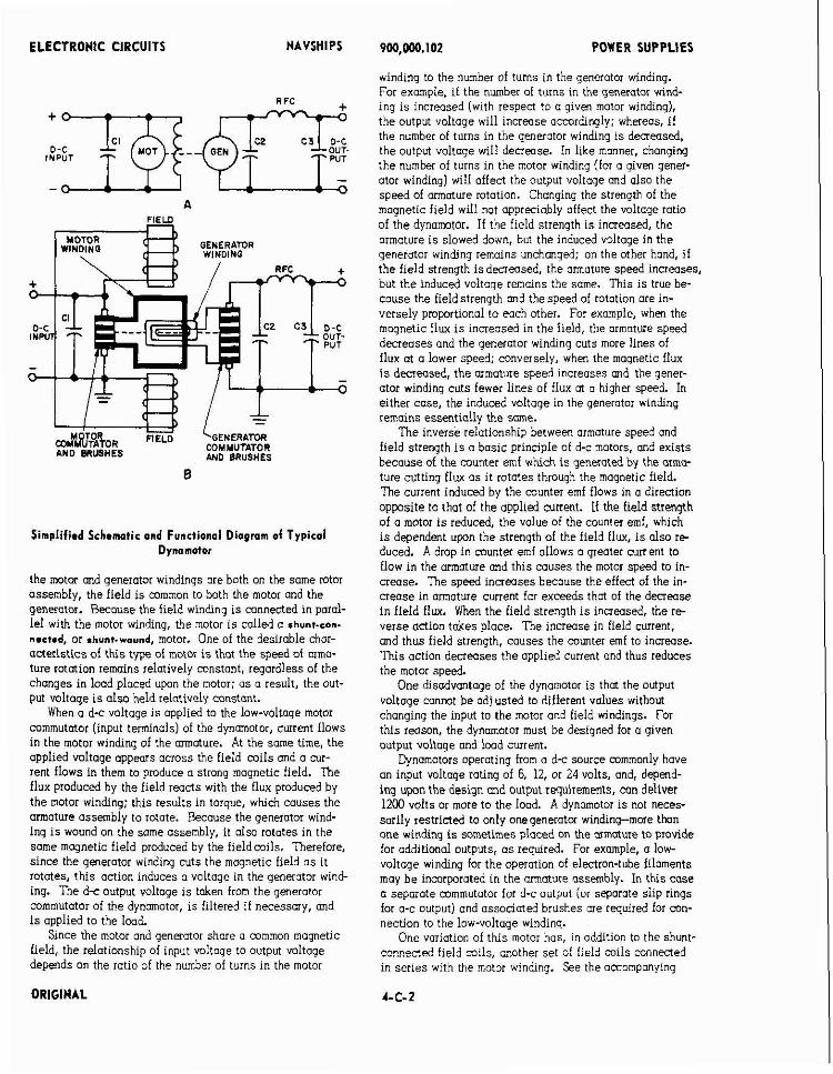
ELECTRONIC CIRCUITS NAVSHIPS
FIELD
AND MUSHES COMMUTATOR WD BRUSHES
Simplified Schematic ond Functional Diagram of Typical Dynamotor
the motor and generator windings are both on the same rotor assembly, the field i s common to both the motor md the generator. 6 ~ o u s e the field winding i s connected in parol- lel with the motor winding, the motor i s called a shunt-sen-
nested, or .hunt.xound, motor. One of the desirable cha- acteristics of this type of motor i s that the speed of uno- ture rotation remains relatively constant, regardless of the changes in load placed upon the motor; a s a result, the out- put voltage i s also heel relatively constant.
When a d-c voltage i s applied to the low-voltage motor commutator (input terminals) of the dynamotor, current flows in the motor winding of the armature. At the same time, the opplied voltage appears across the field mi l s and a cur- rent flows in them to produce a strona moanetic field. The flux produced by the held reacts with theflux produced by the motor windina: this results in toroue. which causes the >. . . armature assembly to rotate. Because the generotor wind- ing i s wound on the same assembly, it also rototes in the some magnetic field produced by the fieldcoils. Therefore, since the generotor winding cuts the mognetic field a s it rotates, this action induces a voltage in the generator wind- ing. Tne d s output voltoge i s token from the generator commutator of the dynamotor, i s filtered if necessary, and i s applied to the load.
Since the motor and generator shore a common magnetic field, the relationship of input voltage to output voltage depends on the ratio of the number of tsrns in the motor
900.000.102 POWER SUPPLIES
winding to the number of turns in the generator winding. For examole, if the number at turns in the aenerator wind- . . ing i s increased (with respect to a given motor winding), the output voltage will increase accordingly; whereas, if the number of turns in the generator winding i s decreased, the output voltoqe will decrease. In like manner, chanqing . ~
the number of turns in the motor winding (for o given qener- ator winding) will affect the output voltage md also the speed of m a t u r e rotation. Changing the strength of the mognetic field will not appreciably affect the voltoge ratio of the dynamotor. If the field strength i s increased, the armature i s slowed down, but the induced voltage in the generator winding remains unchangd; on the other hond, if the field strength isdecreased, the atmature speed increases, but the induced voltage remains the same. This i s true be- cause the fieldstrength md thespeed of rotation are in- versely proportional to each other. For example, when the mognetic flux i s increased in the field, the armature speed decreases and the generator winding cuts more lines of flux ot a lower speed; conversely, when the mognetic flux i s decreased, the armature speed increases md the gener- ator winding cuts fewer lines of flux ot o higher speed. In either case, the induced voltage in the generator winding remains essentially the smne.
The inverse relationship between armature speed and field strength i s o bosic principle of d-c motors, and exists because of the counter emf which i s generated by the armw ture cutting flux a s it rotates through the mognetic field. The current induced by the counter emf flows in a direction opposite to that of the applied current. If the field strength of a motor i s reduced, the value of the counter emf, which i s dependent upon the strength of the field flux, i s also r e duced. A drop in counter emf allows a greater current to flow in the armature md this causes the motor speed to in- crease. ?he speed increases because the effect of the in- crease in anature current for exceeds that of the decrease in field flux. When the field strength i s increased, the re- verse aciion takes place. The increase in field current, and thus field strength, couses the counter emf to increase. This action decreases the opplied current and thus reduces the motor speed.
One disbdvantoge of the dynamotor is that the output voltaae mnnot be ad1 usted to different values without changing the input to the motor and field windings. For this reason, the dynamotor must be designed for a given output voltoge and load current.
Eynamotors operating from a d c source commonly have on input voltage rating of 6. 12, or 24 volts, and, depmd- inq upon the design and output requirements, a n deliver 1200 volts or more to the load. A dynamotor i s not neces- sarily restricted to only onegenerotor winding-more thun one winding is sometimes placed on the armature to provide for additional outputs. a s required. For example. a low- . . voltage winding for the operotion of electron-tube filaments may be incorporated in the armature assembly. In this case a separate mmmutotor for d-c output (or separate slip rings for a-c output1 and associated brushes are required for con- . ~
nection to the low-voltoqe winding. One variation of this motor has, in addition to the shunt-
connected fie!d mils, onother set of field mils connected in series with the motor winding. See the accompanying
ORIGINAL
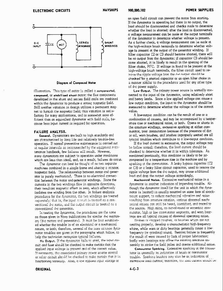
ELECTRONIC CIRCUITS NAVSHIPS
SHUNT
i!!::stratinn. ?his !-c , ~ of motor i s colled c :;m~ms=!ed.
compound, or .tabilir.d shunt motor: the flux components developed in the shunt md series field coils are combined within the dynamotor to produce a strong magnetic field. Still onother vmiation in design utilizes o permanent mag- net to furnish the magnetic field; lhis vmiation i s sotis- factory for many applications, and i s somewhat more ef- ficient than an equivalent dynomotor with field coils, be- muse less input current i s required for operotion.
FAILURE ANALYSIS. G.neral. Dynamotors me built to high standards and
are characterized by long life and reiotjveiy troubie-iree operotion. If normal preventive maintenmce i s curried out a t regular intervils as remmxen?e2 5jj :he eqdipaen: mi:: tenonce hmdbook, few foiiures wili result. However, many dynamotors ore subject to operation under condit~ons which are less than ideal, and, a s a resuit, failures do occur.
Tne dynomotor can best be thought of os two separate machines combined in o single frame and shming o common magnetic field. Tne relotlonsh~p between motor and gener- otor is pureiy mechanicel. There is no electrirnl connec- tion between the motor andgenerotor windings. Since the ;iiner.:s in :he two *<ndinqs flow in vv" ..- -.-- , t v ! , ~ P E L I : ~ : m m ~ ~ t - n'lm 1s 2-r-, +r.c. rl!ec~ J:!.
1s3lates cne w~niinq lrcr t-e 3rncr. :r !=l.urc soly:!~ ..-... .-. I^. ... . -.--.,. ..^. .^ ,..: - - - ..--. ,: . . . . . . . . . . . . . . . .,<. ...~l_l . , . . . . . il . , ,' :, .. . . - .- . . . . . . . A -. . -- . . , . . ..
ventior.nl d i motor, xi? ti.; ;,tp~t it;i;;;it i s treatci :s 2
conventional d-c Generator. i n testing the dynomotor, the proceZiires are the save
a s those given in Navy publications for similm d c machin- cry !j-c motors 2nd jeneratcrs). !I in:! Se ii:~! es!abi!sb- ed whether the trouble i s of on eiectricnl or c mechanical nature, or bath; therelore, severoi of the r m r r mmmon dyna- motor troubles ore given in the paragraphs which foilow, to help the technicim recognize typical failures.
u- n..-... 1 4 tk. A..nnmntnr inile tn ~ t m t the innut r i r - .." -" .v-.. .. .. ..-., .~~. ~~~, ~ ~
cuit and fuse should be checked to make certain that the applied input voltage is piesenr m d of the correc! volue. !! necessmi.. thz z s s o c i a t e ~ z r i x c ~ , 2cwer sosce mntni .- .. !... .:.-.:. .L-..,A L - "L....$,"> ,- --,,.. -".*"<" .h"* < * :" ", LC>"! L.,LU,> b,,""." "C L,,cL?.=u ,- ... "..% --.. -.. , .,-. .. ." functioning normally. Aiso, o i o i appiiea inpill iolroge or
9M),000.102 POWER SUPPLIES
an open field circuit can prevent the motor fmm starting. If the dynmnotor i s operating but there i s no output, the l w d should be disconnected and checks mode to detamine whether the l w d i s shorted; after the l w d i s dismnnecled, a voltme measurement can be made ot the output terminals of the dynamotor to determine whether voltage i s present. As a further check, a voltage mwsurement can be made at the high-voltoge brush terminals to determine whether volt- age i s present at the output of the generator winding. If filter capacitor C2 or U should become shorted, there will be no output from the dynamotor; if capacitor C3 should b e come shoned, i t i s likely to result in the opening of the filter choke, RFC. If wltage i s found to be present at the hiah-voltaae brush terminals, the filter circuit used to r e rrnirZ !he ?ipp!? xl"!!121. !r"m !he A- nlit?ilt shnllld he
checkdfor a shorted capacitor or m open iliter c n o ~ e In il manner s i & h ta the p~roce~ilres used for my other type of d~ power supply.
Lrx Output. ?he Firimary wwer souice i s normnlly can- nected to the input of the dynamotor, using relatively short and heavy leads. Since a low applied voltage can muse a low output mndition, the input to the dynamotor should be measured to determine whether the voltoge i s of the correct value.
A low-output condition can be the result of one or a combination of couses, md may be accompanied by a temper- ature rise or mechrmical noise, or both. Opens or shorts in the armature windings, excessive sparking ot either com- mutator, poor commutation because of the presence of dirt ?roil , worn brushes, md brushes improperly seated are all tvpicai tmibies wNch contribute to a iow-ourpur condition.
If the !wd current i s excessive, the output voltage may k- k 1". . " -1. *I. ,, ,e.,h .,,rm-, ... erefore, the iocd Zrren! .'.odd be checked to determine whether it is within tolerance. As mentioned previously, this condition 1s likely to be oc companied by o temperature rise in the mochine and by spaking at the commutator. A leaky bypass capacitor (C2 or C3) or a leaky filter circuit capacitor, used to remove the rippie voltage from the d c output, muy cause additional lonri nnd drop the output voltage acmrdinalv.
~ c c h o n i c a l ~ o i s s . Excessive mechanical noise in a i y n ~ o t a i s ancther i~dicction of impending trouble. U- though the dynamotor itself (or the unit in which the dpa- motor i s located) i s usually mounted on some form of shock- ZC.;~! sqpr! , to reduce mechanical "!bration a"d mise :~s:;l t i lg !:ox a-n!xe rotation, .:crious &norma! mech- ;ni;al noises :or, sti!! be bwr?, iiestifle?, and trcced !c the source Hiqh mica, on out~f-round or eccentric mm- mitatoi, L:-i .,,,. ,. -. .oh I . cu,,,r.ru.rtu. ----,..- *. segmep.!s, md worn becr- inqs me oil typical muses of abnormal operating noise.
Ymker nr m!pprtn i r l i s k s , or hrusiiea which are nor seating p:aperly, develop a characteristic hiqh-frequenq whine, while worn or dirty k i i n g s generally cause o iow- frequency (or grindingj sound. Ehring failure is frequentiy the result of wear caused by lack of proper lubrication; hod!:l Kern tlwlings m y a!!nw th. ,","!in? "nn"!lli* na-
sembiy to strike the fieid poles and n w t e additional noise. tonmutotc.s Sporklnp. Excessive spaking 01 the commu-
!3t01 i s geneial!~ 3 . inl!carlon of brush or mmmutator L IL PI -,.:-., i-..",.^" - ., ","^ b "" in"irn,inn " i
L,""".c. 0"ULc,*,," ",uo,.Ld ,,,", ".-" "- ".. ". . . eXCeSS1Yd ~ w a CurtenI; inereioie, xzr: CW" airiii n i l v u i ~ us
ELECTRONIC CIRCUITS NAVSHIPS
measured to determine whether it is excessive. As mentioned this condition wlll likely be occompafiied by a
rise in the temperature of the dynamotor. Worn brushes, lock of brush pressure, and brushes not
seating properly are common causes of brush swrking;open coils in the armature assembly will also cause brush spark- ing. Typicol commutotor troubles are high or low segments. on out-f-round or eccentric commutator surface, and a high mica condition. The high-mica condition occurs when the commutator seyments have worn down below the insulating mico separator strips between the copper segments. If any one of the three commutotor conditions mentioned i s found to exist in the dynamotor, the machine will require disas- semby and repair (by the electrical shop), since it will be necessary to turn down the commutator in o lathe and then undercut the mica to a level which i s below the surfoce of the commutator seyments.
Temperat~rs Rise. An excessive temperoture rise i s one of the first indications of trouble. Dynamotors are desirjned for either continuous or intermittent duty, and are rated accordinulv. Occosionallv, a dvnamotor which is rated for . . . . . intermittent duty i s mn cnntinuously; in this case the dyno- motor is not bein" operated in accordance with its desiqn . . rating, ond a temperoture rise may be expected.
An overlocd condition is a common cause far overheat- ing; therefore, the lwd current should be checked to deter- mine whether it i s excessive. Poor ventilation resulting from restricted cooling vents or clogged internal air pop sages can cause a tempeioture rise because of the lack of adequate cwling-oir circulation. Shorts in the commutator segments, shorted turns in the ormture or field windings themselves, or winding shorts to metal ports of the ormoture or frame are oll typical causes of dynamotor heating. Also, worn brushes or high mico on the commutator, or both, con contribute to on abnormal temperoture rise. In any event. excessive heating of o dynamotor should always be con- sidered an effect rather than a muse of trouble.
INVERTER.
APPLICATION. An inverter i s one form of rotary converter, and is used
to change the relatively low voltage of a d-c power source to ac for use by the electricoi Iwd. Depending upon the design of the inverter, the output con be either singlephase or polyphase (multiphose) ac; the frequency of the autput voltage i s generally 60, 400, or 800 cycles. The inverter is frequently used in aircraft, shiphard, and smollsraft op plications where the primory source of power i s dc.
CHARACTERISTICS. Input to inverter i s dc; output i s ac. Requires filtering of input leads to eliminate possible
interference resulting from commutation. A rotating machine; commonly uses two sets of rotors
and stators, one set (rotor and stotor) functioning a s a motor and the other a s a generator.
A-C output mmmonlv obtained bv either of two methods:
W0,000.102 POWER SUPPLIES
output taken from one or more stotlonory armature (stator) windinus.
Frequency of output controlled by speed of rotation. Has fair requlotion chorocteiistics; output varies with
d-c input. Maximum efficiency obtolned when power factor of load
i s near unity.
CIRCUIT ANALYSIS. General. The inverter is a rotating electromechonicol
device for converting direct current into alternating current. The inverter i s a combination electric motor and alternotor; the motor i s the prime mover which produces the necessary rototion of on armature, field, or rotor assembly. BY defi- nition, the winding in which the output voltoge is generated i s called on ormature winding, and the winding through which dc is passed to produce on electiomagnetic field is called the f ield winding.
Inverters fall into three general classes, depending upon the ol- generator design. These classes ore coiled the rototinp~r rovolvingormoture, the rototinpar revo lv ing
field, and the inductortype otternotor. In the rototinq or revolvinguimoture a-c generator, the
stotor provides a stotionory electromagnetic field. The rotor, octing a s the ormoture, revolves in the magnetic field, cuttinq the lines of force, and produces the desired output voltoge. The armature o-c output i s token through slip rings and brushes. One limitation of this type 01 generator is that the output is taken through sliding contacts (slip rings ond brushes); therefore, this type of machine i s usually limited to low-power, low-voltoge applications.
?he rototiny or revaivinq-field a-c yenerator i s most widely used. In this type of machine, current from a d-c source i s passed through slip rings and t~rushes to field coils wound on a rotor. Thus, a mounetlc field is produced in the rotor of fixed polarity, and, since the rotor is driven by the motor, o rotating magnetic field i s created. The ro- tating mognetic field extends outword nnd cuts the stationary ormoture (stator) windinus: as the rotor turrs, ac is produced in the stationary windings. The output is taken from the stationary windings, either single-phase or polyphose. through the output terminals to the load without the need foi slip rings and brushes.
In the inductor-type alternator, a field (exciter) winding and an armature windinu ore both cantoined within the some stator frame. Tne rotor, including its pole pieces, is mode of soft-iron laminations. DC is supplied to the field (exciter) windinq, thus establishing o mgnetic field in the stator. As the rotor revolves, the pales of the rotor become aligned with the poles of the stotor, and maximum flux density i s produced. As the poles move out of oliqnment, the flux d e creases. The sinusoidai increase and decrease in maqnetic flux in the rotor and stotor as the rotor rotates induces on alternating voltage in the stotionory armature windings. The a-c output i s token from the stationary armature windlngs without the need for slip rlngs and brushes. This type of machine i s frequently used to generate sinqle-phase, high- frequency ac.
ORIGINAL
ELECTRONIC CIRCUITS NAVSHIPS
The frequency of the o-c yenerotor voltage depends upon the speed of rotation of the rotor and the number of pairs of poles in the machine. Tho1 IS:
where P is the numter of poiis of poles, and rpm i; the revolutions of the rotor per minute. The following examples are provided to illustrate the use of the formulo in solving for rpm, F, and P.
Alternators ure generally design& wit5 o multipole rotor ond a multiple stator; Sowever, for simplicity, the first
,!!I C ~ S j l l l r 2 mi , r i;r??q,G:,Di -.i.<;ng ""I.) " '"a- pole rotor and a two-pole stator. In this mochine one com- ulete cycle of 2-c voltaqe will be inducer! i n the armature windinq for each complete revel-tion o! the 10:31 os it passes .mdrr i j e two jrloiin dxli b u ~ t i i ) pi):e3 i.i ti,? stitor. , .. ?\"en tire rotor of this simpir m ~ i l ~ i n e iaioies oi o i i ie ;: 3600 rpm, the frequency (in cps) of the o-c output wltoge 1s easily fo,md by using !he basic !ormula. Thus:
If six poles ore D ~ O Y ~ G P - : on tne lotor an i on the stator oi an 3-c generotor, then durlny each revo!~tinn ench pnlr of rotor poles passes under three poiis of stator pales, ocd thus generates three complete cycles of o-c output. Sir;ce there ore three poirs ci poles pmvi4ed on the rotor, ?I ioilnws that three times os many cycles will be yeneroted duriny one rotor revolution a s will be for a single pair, or a total oi nine cycles. Assuming ogaln tho1 the output frequency is 60 cps, the rqmre i rpm of the rotor may be found transposing the basic formula to solve Lor rpm. Thus:
T h i s .... example cleariy iliijstrotes the inverse relotioriship .xistinq betwem thp S:,~P,! n! 10t111 rctntlac ond the number of par; oi poies 01 t?r a1tPr;ator. For tne same output . . , , , . , z:q"cnq sz ;c ::,e 1::z: excr.p:: ;22 yz;, "!:!eE ::!? !!z:.L=: . . . . , ,
"1 ""I ,C "l n i . o i .,-.i i" -.,lll.l. I . , . . , i . .,: i : , , i i i ! i
900,000.102 POWER SUPPLIES 1 required rpm of the rotor was decreased by one third, that is, !rum 3600 to 1200 rpm.
When the speed oi rotor rotoiion nnd the miltput frequency of the clternotor are known, the nunber of pole wirs is eosiiy found. For eiiample, if F 1400 cps ~ n d the rotor rotation i s 3002 rpm, then the n g m t e i of pairs of pales is '-..-A '-I,",.,". Lu",," "<
When the lwd on o yenerator is changed, the terminal voltage varies with hod. The amount of variation depends on the design of the qenerator and the power factor of the load. Unless the load i s fixed and constant, some fonnof voltage regulation is necessary to maintain the output volt- aye relatively mnstant under conditions of varying bud. In practice, once a machine i s designed and built, the outpul voltage i s controlled by varying the d-c excitation ita age applied to the field winding. When an n-c yenerotor is
:---> :.L -..-,..... ,L,. .",",,",", ,,--- +,,o -.,. -- . ... - - . > -- - - . "":: .' l, 'j"." .......... .-; -. ..r-l - - ourpiit voitvge which i s to be reyulotei! os o sensing volic:~ to control the amount of current used to excite tne field.
Tne aperation of a typlcol regulotlon system can 'be briefly explcined os follows: a drop in output voltone sensed by the regulotar causes the ieyulotor to incrffise :he field current, and on increase in field current couses a correspnd- ?ng increase in outpgt wltnye to compensate ior the orlylnai drop in output voltage. Stated mnverselv, if the output volt- aye should rise, the reqdotor decreases the field current, causlng o correspondmy decreose i n output voiroye to som- pensate for the original rise in witoge. n u s , t ie rewlfltor senses o change i n output voltage ond compensates tor this uti~nge oy alterln~ tine iieid jexcitinjj cuiiii?~ oimrdinjij.. A detailed desniption of the construction ond oprotion of various voltaqe regulators can be lound in Navy publications - - . . -. , - . . . . -. . .- ...... XS:C e:ectr;c::y, z: :I CC..::LZ :::-~!r~:?is !,I,: r'l - - A AL-.".:..,. """ .' ." ..,,y S.
:rc;zc: : r,<:; :*;; 8::: :* :;;:-;.:g L : : d T r ::. ::,c porotjrap'ns that ioiloa. .. ~" " , * - 7 : . 3: :ts s:xyiest inverters is :Re prrmuner!i-rnqr~ri-type i!lueiiei shown in the ~icoiitp~nyiilz ;c::c~;t;c. T?,i; :o:z!:na-!irk- type jn.v~i:ei i j ?esiji.ed tz siicpIy si-;le;hhie 2- 3: 2
frequency of elther 400 or 800 cycies to o constant and relativeiy liyint ioad.
inverter ronslsts of o 3-c motor and o Germaner,:- moynet-type o c generator nssembly combinel within a sincle - ?c.isilq. !ne 4-c motor i s o shuqti.annecred, or shunt-
. . . . . ~ . ..... "2 --. * " "rn" ... ..".! .... mm ................... ^, ... .i ...... ,.--. ", ...-.-. " -- ...- . . . . ^ i"".. "". ."...:",. ,M;;;.;., ;:.- .;,7;:,r ....>... !:i!,i :;:i:,?i',
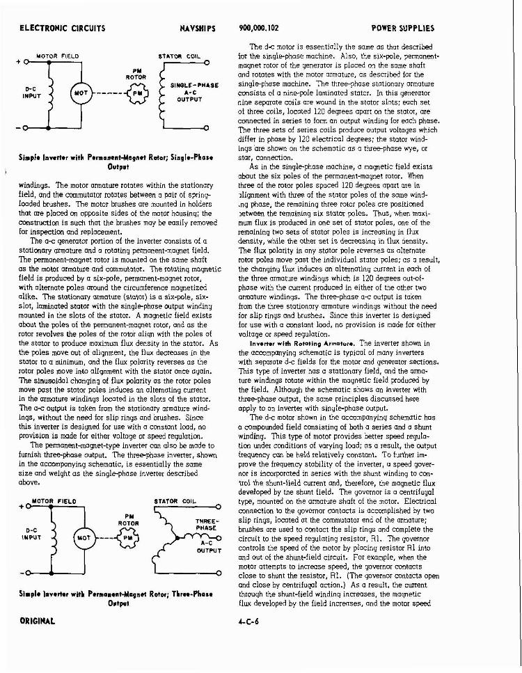
ELECTRONIC CIRCUITS NAVSHI PS
MOTOR FIELD STLTMI COIL
SIWLE-PULSE
INPUT OUTPUT
Simple Inverter with PemosentUogn*t Rotor; Simple-Phase
I Output
windings. The motor armature rotates within the stationary field, and the commutator rotates between a pair of spriny- loaded brushes. The motor brushes are mounted in holders that me placed on opposite sides of the motor housing; the construcficm i s such that the brushes may be easily removed far inspection and replacement.
The a s generator portion of the inverter consists of a stationary armoture and o rotating permanent-magnet field. The permonent-magnet rotor i s mounted on the some shaft a s the motor armature and commutator. The rotating maynetic field i s produced by a six-pole, permanent-magnet rotor, with alternate poles mound the circumference magnetized alike. The stationav armature (stator) i s a six-pole, six- slot, laminated stator with the singlephase output winding mounted in the slots of the stator. A moyetic field exists about the poles of the permonent-mayet rotor, and a s the rotor revolves the poles of the rotor aliqm with the poles of the stator to produce maximum flux density in the stator. As the poles move out of alignment, the flux decreases in the stator to a minimum, and the flux polarity reverses a s the rotor poles move into alignment with the stotor once again. The sinusoidal changing of flux polarity a s the rotor poles move past the stator poles induces an alternating current in the armature windings lacoted in the slots of the stator. The o-c output i s taken from the stationary armature wind- ings, without the need for slip rings and brushes. Since this inverter i s desiyned for use with o constant lmd, no provision is made Lor either voltage or speed regulation.
The permanent-mamet-type inverter can olso be made to furnish three-phase output. The threephose inverter, shown in the acmmpanying schematic, is essentially the some size and weight a s the single-phase inverter described above.
MOTOR FIELD +O + 1
Simpl* 1awrt.r with P*mom*ntMopnet Rotor; Thm-Phase Outp.1
900.000.102 POWER SUPPLIES
The d-c motor i s essentially the same a s that described for the singlephase machine. Also, the six-pole, permonent- maunet rotor of the qenerotor i s placed on the some shaft and rotates with the-motor ormat"re, a s described for the single-phase machine. The threephase stationory armature consists of a nine-pole laminated stotor. In this generator nine sewrote mils are wound in the stotor slots: each set of three coils, located 120 degrees oport on the stotor, ore connected in series to form an output winding for each phose. The three sets of series coils produce output voltages which differ in phase by 120 electrical degrees; the stotor wind- ings are shown on the schematic a s a threephase wye, or star, connection.
As in the sinalephase machine, a maunetic field exists . . about the six poles of the permonent-moynet rotor. When three of the rotor wles swced 120 demees apart are in llignment with three of the stotor poles of the same wind. inu ohase. the remainina three rotor wles are wsitioned .. . =tween the rem.aininq six stator poles. Thus, when maxi- mum flux i s produced in one set of stotor poles, one of the remaining two sets of stator poles is increasing in flux densitv, while the other set i s decreasinq in flux density. The fl& polarity in any stotor pole reveries as alternate rotor poles move w s t the individual stotor poles: os a result, the changing flux induces an olternoting current in each of the three ormatwe windinqs which is 120 deqees out-of- phase with the cunent pr;duced in either of the other two armature windings. The three-phase oc output i s taken from the three stationary armoture windings without the need for slip rings and brushes. Since this inverter i s designed for use with o constant lmd, no provision i s made for either voltage or speed regulation.
Invencr with Rotating Armature. The inverter shown in the accompanying schematic i s typic01 of many inverters with separate d c fields for the motor and generator sections. This type of inverter has a stationary field, and the armo- lure windings rotote within the magnetic field produced by the field. Although the schematic shows an inverter with three-phase output, the same principles discussed here apply to an inverter with single-phase output.
The d c motor shown in the accompanying schematic has a compo~mded field consisting of both a series and a shunt winding. This type of motor provides better speed reyulo- tion under conditions of varying lwd; a s a result, the output frequency can be held relatively constant. To funher im- prove the frequenq stability of the inverter, a speed gover- nor i s inmrporoted in series with the shunt winding to con- trol the shunt-field current and, therefore, the magnetic flux developed by the shunt field. The governor i s o centrifugal type, mounted on the armature shaft of the motor. Electrical connection to the governor contocts i s accomplished by two slip rings, located at the commutator end of the armature; brushes are used to ccmtact the slio rinus and comolete the . . circuit to the s p e d regulating resistor. R1. The governor controls the soeed of the motor by placino resistor R1 into . . ond out of the shunt-field circuit. For example, when the motor attempts to increase speed, the governor contocts close to shunt the resistor, R1. (The governor contacts open and close by centrifuqal anion.) As a result, the current through the shunt-field winding increases, the maynetic flux developed by the field increases, and the motor speed
ORIGINAL
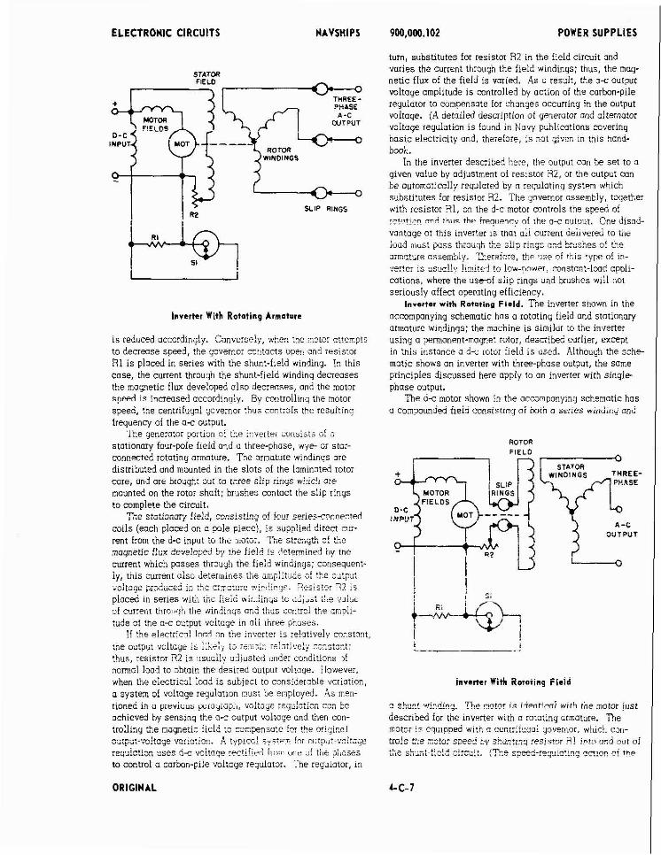
ELECTRONIC CIRCUITS
STATDR
ROTDR WINDINGS
Inverter With Rotating Amotvrc
is reduced accordinyiy. Converseli., ,#Den 1% :go!cr attempts to decrease speed, the governor a? tac t s open ond resistor Rl i s ploced in series with the shunt-field winding. In this case, the current through the shunt-field winding decieoses the magnetic f l u developed also decreases, and the motor speed i s increased accordinoly. Bv mntrollinq the motor speed, the centrifugal yovernoi t ius ccatrols the resuitiny frequency of the a c output.
Tne generator po:tion of !Re i:;verter ~zc~risl~is 6: ;
stationary four-pole field and u three-phase, wye or star- connected rotating armature. The armoture windings ore distributed and mounted in the slots of the lominoted rotor core, and ore brought uut to three slip rings wilich are mounted on the rotor shaft: brushes contact the slip rinqs ~. to complete the circuit.
3 e a:;:ionnr# !ield. ccnsis t i~g of fsur c~riescnnnerred coils (each placed on 3 pole piece), is supplied direct cur- rent from the d-c input io tiit. motor. The si;e,yth, a! the mopetic flux de,ieloped by the fie!< is determined hy tne current which passes through the field windings: consequent- iy, this current aisu deteriiiinei ihs ~zp! i tu l i ;! t5e o;:~;: io:ijqe aro?lie~ .., < - ." ..... .,...>..... . . . ;- . l:~. .c ... ; .. .,.. ?esistr.r 1 2 1; . ~
placed in series w l t i ize lieid i*l:.ii:~~s to uij,s: :!.e i;:,i of omrent thro~ir!t, the windinus on2 thus control the srncll- tiide at the c c output voitoge in oii inree phoses.
Ti the e!ec!rien! !nod nn t k iin.:er!e: is re!ativelv constag!, Lr,e output volturjr i i :I;%:, 13 ;;,i.;li r-r!s:is.e>f :;:st:::: thus, resistor R2 is usdoily orliusted under conditions ,f normal load to obtain the desired Output voituue. fiowevei. when the electrical loo!. is subject to considrrabie variation, a system of valtage regulation must he employed. As men- tioned in o previuub p ~ r ~ ~ i i i p i ~ , .vck;j; :iijli!ztion CCE bz achieved by sensing the a-c output voltage and then con- trolling t+e mayeti; field to -3-penscte f-.r the ori,:i~a! -...-..a . . .^ l*^-~ \rn.i",i,,., A tsjr, ;,-,,I 5"<:em !n: n#jtg,,t.,".fl!t:qe "U%YU. .-.. "lJ" . . _, i... , ;e;;-laticn 3s.s 6- .,olmqe r.?c!iiir,i :,<,:,I ur,e u f titi. o;,ajej
to control a carbon-pile voitoge regulator. ihe reguiator, i n
9M).OM).102 POWER SUPPLIES
turn, substitutes for resistor R2 in the field circuit and varies the current through the field windings; thus, the mag- netic flux of the field is varied. As o result, the a c output voltage amplitude is controlled by action of the carbon-pile regulator to compensate for changes occurring in the output voltage. ( A detailed description o: qenextor ond alternator voltoge regulation is found in Navy publications covering bosic electricity and. therefore, i s not qivcn in L%is hand- book.
In the inverter described here, the output can k set to a qiven volue by odiustment of resistor R2, or the output con be outomciticdly reyulored by o :egulatinq system which substitutes !or resistor 92. The qovernor ossernbly, together with resistor Rl, on the d-c motor controls the speed of !n!n!i"l rind ?hi)+ t h ~ ! ~ e q , > e n ~ of the o-c outout. One disod- vantage ot thls lnverter is t n a ~ oii current driivered to tire luud oiusi pass thi-iiqh ;he s!i? r i n ~ s c:d brushes cf the aimoture cssembly. Dereiorn, <he *QS? of ?is type of in- ve:!er i s ssual!v limited to !"w-nnw~r mnstont-lwd opoli- cations, where the u s m f slip rings and brushes will not seriously affect operoting efficiency.
Inverter with Rotatinp Field. ' h e inverter shown in the accompanying schematic hos a rotating field and stotianary armature windings; the machine i s similar to the : ,nierter . using a permanent-magnet rotor: described earlier, except in this instance a d-c rotor field is used. Although t+e s c h e motic shows an inverter with three-phase output, the same principles discussed here apply to an inverter with sinqle- phase output.
The d c motor shown in the accornponyiny schematic has u compounded iieid consisr~ng oi k i n a series n ~ j d l o g on;
ROTOR
- STATOR
W I N D I N G S THREE- PHASE
O U T P U T
r' L--O
? she! ui.qdin;. Tk mntni ic identlmi wirh the motor just described for the inverter with o rorating armature. 3 r motor 1s enwpped wit? a cenrriixol governor, wtiicil coo- ::c!s :% .33!or s x c ? t~ she t in7 TPSi5lor ? i !ntn rand our of . . ' I i7.in c"nni.r~,n.inl,n,, "rtlnn " i ,lp ,/,S DiiYill I i..- "F---- ._,_.l_ ... ? -.
ORIGINAL
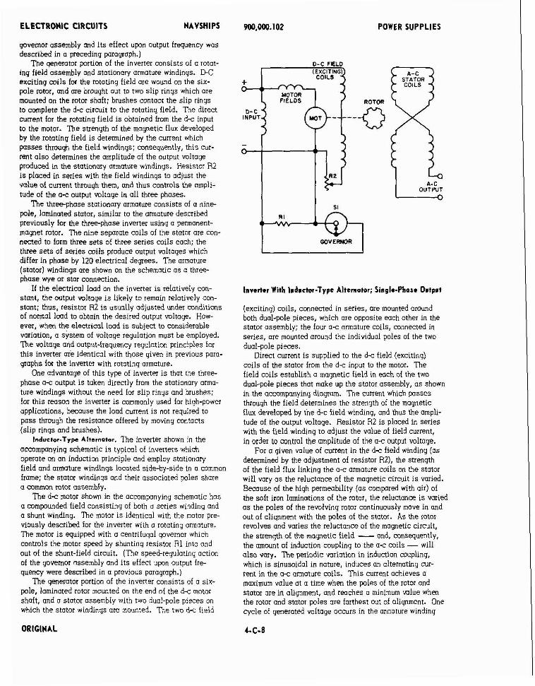
ELECTRONIC CIRCUITS NAVSHIPS
governor assembly md its effect upon output frequency was described in a preceding paraq1aph.1
The aenemtor mrtion of the inverter consists of o rotat- ing field ossembly and stationary armature windings. D C excitinq coils for the rototinq field are wound on the six- pole rotor, and are brought out to two slip rings which are mounted an the rotor shaft; brushes contact the slip rings to complete the d s circuit to the rototinq field. The direct current for the rotating field i s obtained from the d s input to the motor. The strength of the magnetic flux developed by the rotating field i s determined by the current which passes through the field windings: mnsequently, this cur- rent also determines the amplitude of the output voltage produced in the stationary armature windings. Resistor R2 i s placed in series with the field windings to adjust the value of current through them, and thus controls the ampli- tude of the a-c output voltage in all three phases.
The three-phase stationary armature consists of a nine- pole, laminated stator, similar to the armature described previously for the threephose inverter using a permonent- magnet rotor. The nine separate coils of the stator are con- nected to form three sets of three series coils each; the three sets of series coils produce output voltages which differ in phase by 120 electrical degrees. The ormature (stator) windings are shown on the schematic a s a three- phase wye or star connection.
If the electrical load on the inverter is relatively con- stant, the output wltage i s likely to remoin relatively con- stant; thus, resistor RZ i s usually adjusted under G d i t i o n s of normal load to obtain the desired output wltage. How- ever. when the electrical load i s subiect to considerable variation, a system of voltage requlation must be employed. The voltaue and outout-freauennr reuulotion orincioles for . , - this inverter are identicol with those given in previous poro- graphs f w the invmer with rotating armature.
One advantage of this type of inverter i s that the three- phose a s output i s taken directly from the stationary arma- ture windings without the need for slip rings and brushes; for this reason the inverter i s commonly used for high-power applications, because the load current i s not required to pass through the resistance offered by moving contacts (slip rings and brushes).
Inductor-Type Alternator. The inverter shown in the accompanying schematic i s typical of inverters which operate on an induction principle and employ stationary field and armature windings located side-by-side in a common frame; the stator windings and their associated poles share a mmmon tator assembly.
The d-c motor shown in the accompanying schematic has a compounded field consisting of both a series winding and a shunt winding. The motor i s identical with the motor pre- viously described for the inverter with a rotating armature. The motor i s equipped with a centrifuijol governor which controls the motor speed by shunting resistor Rl into and out of the shunt-field circuit. (The spee®ulotinq action of the qovernor nssembly and its effect upon output fre- quenq were described in o previous paragraph.)
The yenerator portion of the inverter consists of a six- pole, laminated rotor mounted on the end of the d-c motor shaft, and a stator ossembly with two duol-pole pieces on which the stator windings are mounted. The two d-c field
POWER SUPPLIES
Inverter With Indrctor-Type Alternotor; Single-Phase Output
(exciting) coils, connected in series, are mounted around both duol-wle pieces. which ore oo~osi te each other in the . . . . stotor ossembly; the four a-c armature coils, connected in series. ore mounted orouxd the individual ooles of the two dual-pole pieces.
Direct current i s supplied to the d-c field (exciting) coils of the stator from the d-c input to the motor. The field coils estoblish a magnetic field in each of the two dual-pole pieces that make up the stator assembly, a s shown in the accompanying diagom. The current which posses through the field determines the strength of the magnetic flux developed by the d-c field winding, and thus the ampli- tude of the output voltage. Resistor R2 i s placed in series with the field winding to adjust the value of field current, in order to control the amplitude of the a-c output voltage.
For a given volue of current in the d-c field winding (as determined by the adjustment of resistor RZ), the strength of the field flux linking the a c armature coils on the stator will vary a s the reluctance of the magnetic circuit i s varied. B w u s e of the high permeability (as compared with air) of the soft iron laminations of the rotor, the reluctance i s varied a s the poles of the revolving rotor continuously move in and out of oliqment with the poles of the stator. As the rotor revolves and varies the reluctance of the magnetic circuit, the strength of the maynetic field - and, consequently, the amount of induction coupling to the a-c mils - will also vary. ?he periodic variation in induction coupling, which i s sinusoidal in nature, induces an alternating cur- rent in the a s armature coils. This current achieves a maximum value at o time when the poles of the rotor and stator are in alignment, and reaches a minimum d u e when the rotor and stotor poles are farthest out of aliynment. One cycle of generated voltage occurs in the armature winding
ORIGINAL
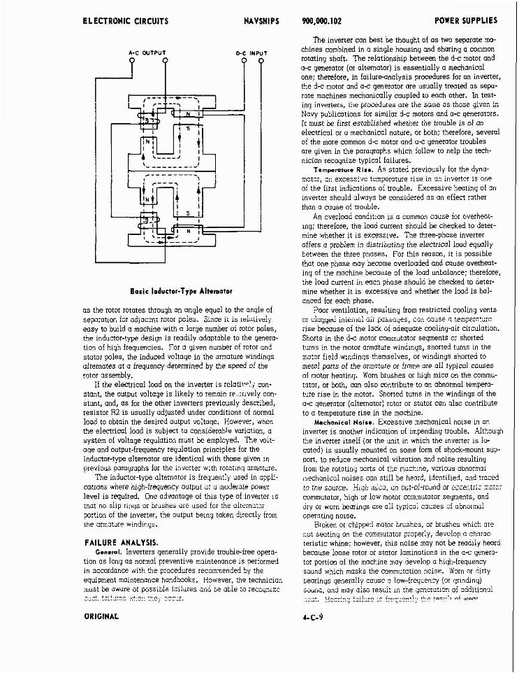
ELECTRONIC CIRCUITS NAVSHIPS
D-C INPUT
P P
Basic Isductor-Type A l t e n a t o ~
a s the rotor rotates through on ongle equal to the angle of seporomn for odpc-nr rotor poies. S i ~ c e ii i s :;iuiivriy easy to build a machine with o large number of rotor poles, the inductor-type desirjn i s readily adaptable to the genero- tion of high frequencies. For a given number of rotor and stator poles, the induced voltage in the armature windings alternates a t a irequency determined by the speed of the rotor assembly.
If the electrical lwd on the inverter i s relativ-!; con- stant, the output voltage is likely to remain re.~t,vely con- stmt. and, a s for the other inverters previousl~ desctibed, resistor RZ i s usually adjusted underconditions of normai load to obtain the desired output voltage. However, when the electrical lood i s subject to considerable variation, a system of voltoge regulation must be employed. ' h e wlt- aqe and output-frequency regulation principles for the inductor-type alternator ore identical with those given in previous paragraphs for the inverter with rototiny atmotare.
' h e inductor-type alternator i s frequently used in cppli- cations where high-frequency output a t a moderate power level i s required. One advantage of this type of inverter is cnai no 511p rings or brusnrs are used for (he airernotoi portion of the inverter, the output being token directly from me ormoture windings.
FAILURE ANALYSIS. General. Inverters generally provide troublefree opero-
tion a s lonq a s normal preventive mointemnce is performed in accordance with theprocedures recommended 5; the equipment maintenance hondboks. However, the technicion
POWER SUPPLIES
The inverter can best be thought of a s two separate ma- chines combined in a single housing and sharing a common rotating shoft. The relationship between the d c motor and a s generator (or alternator) i s essentially a mechanical one: therefore, in failurmnolysis procedures for an inverter, the d-c motor and o c generator are usually treated a s s e p - rate machines mechanically coupled to each other. In test- ing invrrirrs, lilr procedures are the same a s those jive; i; Navy publications for similar d-c motors and a s generators. It must be first established whether the trouble is of an electrical or o mechanical nature, or Loth: therefore, sever01 of the more common d-c motor and a c generotor troubles ore given in the paroqaphs which follow to help the tech- nician recqnize typical failures.
~ s ~ ~ ~ ~ a t ~ ~ s ~ i s e . As stated previously for the dyna- --. :..,.cr, 3ri excessive tenpersture rise in m irverter is one
of the first indications of troubie. Excessive heating of an Inverter should always be considered a s on effect rother than a cause of trouble.
An overload condition is o common cause for oveineat- my: therefore, the lood current should be checked to deter- mine whether it i s excessive. The threephase inverter offers a problem in distributing the electrical lwd equally between the three phases. For this reason, it i s possible that one phase may become overloaded and cause overheat- ing of the machine because of the laid unhionce; therefore, the lwd current in each phase should be checked to deter- mine whether it i s excessive ond whether the lwd i s bol- onced for each phase.
Poor ventilation, resulting from restricted cwling vents a; ciag4r: ioiei:io: air pxajarej, iifi cGije a tem?;c:l;;2 rise because of the lack of adequate cwiing-air circuiation. Shorts in the d c motor commutotor segments or shorted turns in the motor armature windings, shorted turns in the notor field windings themselves, or windings shorted to metal parts of the armature or frame are all typical rouses of motor heating. Worn brushes or high mica on the commu- tator, or both, mn also contribute to an abnormal tempera- ture rise in the motor. Shorted turns in the windings of the a c generotor (alternator) rotor or stator can a lw contribute to a temperature rise in the machine.
~ * ~ h a ~ i c o l ~0i.e. Excessive mechanical noise in an inverter i s another indication of impending trouble. AIthough me inverter itself (or the unit in which the inverter is lo- coted) i s usually mounted on some form of shock-mount sup- port, to reduce mechanical vibration ar.d noise resulting from the rotating parts of the machine, vorious abnornol mechanical noises can still be heard, identified, ond tmced to the source. High mica, an out-ol-round a eccsrrtrii zoti; commutator, high or low motor commutotor segments, and i iy or worn bemmgs are d i iypicol CoYSes of c h o r r d Operatinq noise.
Broken or chipped motor brushes, or bushes which are not seating OE t ie commutotor properly, develop a charac- teristic whine; however, this noise may not be readily heard because loose rotor or stator laminations in the o-c genera- tor portim of the machine may develop a high-frequency sound which masks the commutotion noise. Worn or dirty hearings generoliy cause 3 low-frequency (or yrinding) sound, and mciv olso resai: in the gcr.c:at:on o! oddiiionai
ORIGINAL
ELECTRONIC CIRCUITS NAVSHIPS
caused bv lock of proper lubriation; badly worn bmrinqs may allow the roto; assembly to strike the' stator and crizte additional noise. Furthermore, a rotor which is not centered in the stator bemuse of worn bearings, olthough it may not strike the stator, i s likely to cause some localized heating in the stator.
Motor Cornmutotor Sparking. Excessive sparkiny at the motor commutator i s generally an indication of brush or commutator troubles. Sparking brushes may olso be an indi- cation of o m or shorted coils in the armature windinq, or M indication of o grounded, open, or shorted field winding. As mentioned previously, this condition will likely be ac- companied by a rise in temperature of the machine. Worn bmshes. lock of brush pressure, brushes stickinq in their holders, or brushes not seating properly are also causes for sparking.
Typ ia l d-c motor commutator troubles are hiyh or low segments, an out-of-round or eccentric commutator surface, or a high mica condition. (The high mica condition occurs when the commutator seqments have worn down below the insulating mica separator strips between the copper swj- ments.) If on" one of the three conditions mentioned is found to exist in the motor commutator, the machine will require disassembly and repair (by the electrical shop), since it will be necessary to turn down the commutator in a lathe and then undercut the mica t o o level which i s Lelow the surface of the commutator segments.
No output. If the inverter fails to stun, the input circuit should be checked to make certain that the applied d c voltage i s presmt and of the correct volue. If necessary, the associated primary power sourcp cone01 or relay circuit should be checked to make certain that it i s functioning normally. A low applied input voltoge or an open field circuit a n also prevent the motor from stortinq.
If the inverter i s running but there i s no output, the lwd should be disconnected ond checks mode to determine wnether the lwd i s shorted; a voltage measurement can be made a t the output terminals of the a-c generator after the load i s disconnected to determine whether voltage i s pre- sent. In the m s e of the threephase inverter, measurements should be made on each of the three phases. 'With the in- verter d ismmened from its input and output circuits, con- tinuity measurements can be mode in accordance with the equipment maintenance handbmk instructions to determine whether any of the windings ore open.
Low Output. A low-output condition can be the result of one or a combination of causes, and may be accompanied by a temperature rise or mechanical noise, or both. Low input dc to the exciter mils, poor slip ring contact bemuse of the presence of dirt or oil, worn brushes, and improper brush tension are typical troubles which contribute to a low-output condition.
Shoned windinqs can cause low output, and this mndi- tion i s nwrly olwoys accompanied by a temperature rise in the inverter. If the load current i s excessive, the output voltage may be below normal; therefore, the load current should be checked to determine whether it i s within toler- ance. For the threephase yenerator or alternator, the lwd current for each phose should be checked to determine whether it i s within tolerance and whether the load i s k l - cnced for each phose. As mentioned previossly, nn unbal-
ORIGINAL
90O.WO.102 POWER SUPPLiES
once in the load of tb,e three-phase mochlne is llkeiy to cause o tempeioture rjse in the machlne.
A low-outp-t csndition car: aisa te coused by a decrease in the current through the excitinq field; a s a result, the magnetic flux in the field decreases and the outprrt voltaije decreases accordingly. If the d-c (exciting) field current i s controlled by o voltage regulating system, it is possitle thot the system i s foulty. If the field current i s established by means of on adjustable reslstor (resistor R21, it i s pas- sible that the value of the resistor is too hiyh. In the case of the inverter with rotating field, the slip rings and brushes may cause this conditim bec~use of excessive contact resistance.
Hlah 0 ~ 1 ~ ~ 1 . .4 hiah-output cor,dition i s U S I I ~ I Y caused by an excessive current in the exciting field: as a result, the maqnetic flux in the field increases and the output volt- age inneases accordingly. Ii the d-c (excitinq) field cur- rent i s controlled by o voltaoe reouiatinu system, it is ws- . ~ - . sible that the system i s faulty. If the field current i s established by means of an odiustable resistor (resistor R2), i t i s passible thot the volue of the resistor is too low.
unsteady output voltage. The cause of unsteady or iluctuotiny output voltaye, sometimes called ~o1rn.e hunting.
varies, depending on the design of the inverter and the method inmrporoted in the mocnine to regulate the volue of the output voltage. If the output voltoye fluctuates (assum- ing the speed of rototion to be relatively conslont), this condition may be caused by fluctuations of the current in the excitinq field; a s o result, the magnetic flux in the field will olso fluctuote. This condition may also be caused by a defective voltogeregulating system (mentioned pre- viously under the hiqh-output and low-autput conditions discussed above), or, if the inverter has o rotating field, the slip rings and brushes may not be in good contact with each other.
Unstsody or Incorrect Output Frequency. The muse of unsteady output frequency, sometimes coiled frequency
hvnting, or simply hunting, and the cause of incorrect out- put frequency varies, depending on the design of the inverter ond the method incorporated in the machine to regulate the speed of rotation. If the speed of rotation fluctuotes, the output frequency will olso fluctuate, slnce the speed of the rotor determines the frequency of the olternqti,ns in the ormature windings. Thus, if the rotor speed is k low normal, the output frequency will also be below normal, and, con- versely, if the rotor speed is o h v e normol, the output i r e auencv will olso be obove normal. If the d c motor has a . . centrifugalipvernor assembly, the governor contacts, slip rings, ond brushes should be inspected for possible defects. Instability in the motor speed may also be evidenced by mechanical noises, temperature rise, brush sporkinq, etc, mentioned earlier in this discussion.
VIBRATOR-TYPE POWER SUPPLIES. General. The primory eiectricnl power source in many
portable and mobile (smoll h a t s , light nitcraft, and yround vehicles) electronic equipments i s a storaqe kttery.
~ ~
vibrator-type power supplies ore used to convert direct current from the storage battery to alternating current which can be rectified to furnish high-voltoge ior the operotion of the qtipiilent. Vibrator-type power suppi i~s are designed
L C - 1 0
ELECTRONIC CIRCUITS UVSHIPS
for opmtion with specific input voltages: storage batteries having voltage values of 6, 12, or 24 volts are commonly used to operate this type of supply.
The main differences between o conventional power s u p ply operatiny from an a c source and a vibrator pwer s u p ply are the vibrating device used to convert the low d c ya!:cge tc Ligh o e ~l!a:e I"? th? s?e"cinl ste-p wwer transformer used in coniunitian with :be vibrator. The vi- brator i:self i s essentially a high-speed reversing switch that alternately opens and closes sets of contacts in the primary circuit of the power transformer. ' h e rising and falling magnetic field caused by the current pulses in the transformer primary induces on alternating square wave in the secondary circuit. The vibrotor i s designed to operate at a p e n ireqoency, usuoliy Leinciu 6: cid 2% :jc!ec per second, although in some applications higher frequen- cies are employed.
Two basic vibrators ore widely used in power supplies ,,,, ,"*el- oi t i i s type; one is csile6 ;he a ~ n t ~ n c h r o a o u s :^- '
rupter) Vibrator, and the cther i s called the ~ ~ n c h r a o u s
(or *elf-ractr+mp) vibrator. The primary function of either type of vibrator i s to cause the d c input current to flow in ~ u l s e s through alternate halves of the transformer primary. The nonsynchronous vibrator requires the use of some form of hiyh-voltoye rectifier circuit to produce d c output from the supply. The synchronous vibrator does not requlre a separate rectifier circuit since, as the name .ynchronous
(or s.lf-rectifr~ng) implies, the vibrator itself performs the additional function of rectifying the high-voltage ac it pro- d - - -~ by synchionnu+ swjtchinr! of the transformer second- ary winding; the resulton: output vcltage i s essentially dc.
Occasionally, vibrator power supplies ore designed to operate an more than one voiue of lnput voitoye: this is ocmmplished by provldlny a number of taps an the trans- former primary, and appropriate switching or terminal points to accommodate the different battery voltages.
Several types of vibrator pwer siippiies ore capnble a! operotion from bath a low-voltage d c source and a mnven- tional 6C-cvcle o-c source. A combination power supply of this type is usually q u i p p d with o transformer having a. additional primary windinq for 3-c aperotion; the primary winding used ior vlbrotor operation i s tuppd, and is iised os the filament wiiding fo; the e!ectror lubes when operot- iny on ac. This type of power supply uses a non-synchro- nous vibrator and o separate rectifier ciicu;i, 5iil:e :h2 same hiy"-w:tarjr sc.:a:.J;r; is ~ ~ e . 5 i:r 3-. I?%! ?-: ?peration.
.?zc!ie~ co~hircrion ilr "rid vlbrotoi nowe:-supoly de- sign uses two separate pwer rronsiormers, wlth independent :ez;:be;: in !L: .:jh:q!~~ ciirgi! and i n the sc input circu~t. ;hew c*o indepnie;.: ~ * e r - i j $ f ar:~.ts shxe 2
-on filter circuit tn filter I'nelr respective d-c outputs; either of tile two input circuits i s selected by a switching
arrangement, depending upon whether ds input or c-c irput operation i s desired.
Aithough there are mhri ciiuuii utiuihysT5e:i;s f;; pro viding operation from 'kth o c and d c input sources, the examples given obove are typico!. One oher mmbinction " . - - -.. '.-' .? ---"..--":I.. P.,.!.\,d ",,,LP? ,iSe V:DrULY, >Y/I / I I ) . " i i i i . . .- rrrrr.- ..-... -.-,-- ,.! two .fiba.-- ,,. ,~.,,..es -....- s 8 o~erot:n.; from c mmmnn rk: inwt but with two or more output voltages. The outputs of the
W0.OOO.102 POWER SUPPLIES
combined supplies m n be either positive or neyotive, or 'both, and of different voltage volues.
Any of the cooventicmal electron-tube or semiconductor rectifier clrnuits, such a s the half-wave, full-wave, bridge, and voltoae doubler. mn be used in nonsvnchronous vibrotor power supplies. The use of semiconductor rectifiers sim. ~ l i f i e s the desim of ncmsvnchronous vibrator-type pawer s u ~ l i e s , since nn,blament voltaye i s rwuired for the rectl- fier(s).
NONSYNCHRONOUS VIBRATOR SUPPLY.
APPLICATION. The nonsynch~anous vibrotor supply i s mmmonly em-
-'-..-A ' - ---.. m-t-hl- mnA m n h i l ~ eqtinlipments where the r.l,-- ... - ~ ~
~rimarv wwer source is a storaqe mttery. 3 1 s supply . . produces a relatively hiqh v d t e of di: voltoge at a mdemte Imd cunent from o low-voltaqe d c source. The supply i s cnnmonly used to ?:c%!ide hiyh voltage ior the opemuon of small receivers, transmitters, and public4ddress systems, although in many recext equipment; the transistorized d c tc-dc mnverter, described earlier in this section of the handbmk, i s used in lieu of the vibrator supply.
CHARACTERISTICS. Input 16 low-wltoqe dc; output i s high-voltage dc. Input voltoge i s usually 6, 12, or 24 volts: special vl-
brators for other input voltages are avolloble. Typiml vibrator operating frequency i s between MI and
250 cvcles. Output high-voltage dc i s normoily between 180 and %I
volts; Iwd current i s normally between 60 and 200 milli- 3mperes.
Output ci;iiiit can be arranged to furnish negative or positive hiqh voltage to the imd.
Output dc requires filtering; ripple-voltage frequency i s relatively high, on? i s determined by the vlbrator frequency and the rectifier circuit used.
Electron-tube or semiconductor diodes me used in the rec!!!!~ d r x i t : rectifier circuit mag be half-wave, full- wave, bridge, or wltaqdoubler.
Req~latioz is fd r ; outpdt vdtage regulation mo), be em- :Ioyed.
Vibrator must be shielded and leads filtered to prevent i-: iadia':;;, md !nte:ference to other c!rctllts.
CiRCUlT ANALYSIS. G.n.rol. A nonsynchronous vibrotor supply converts
d~rect current from a low-voltage Fwer source into alter- natinq m e n t that mn be rectified and used to obtain a I;lat,er 3% 3utmt .m!tme !or US? '1s the plate and screm voit- flies ir the operating &,pment. The supply offers the oavontoqes of Uant weiont. snlall ~ h v s ~ c o l size. and dad > . . . efficiency; its main disadvantages are the limitation in outmt current and the tendenw to produce interference to . . :tL.e; -:_:I;. T.::c!xe, ~ 1 0 or -rr! b Y C I J - ~ I I I ~
and shielded. Anovier i iudwntaqe is hot , olthowqh the vibrator itself is relatively inexpensive, i ts useful life i s rhnnar :hon that of 3 dynamotor or oi the mnsistots in a Ac-icxlc imvtiiei . Ko-wsr. ,<hen \?is !;w o! v e r s u p
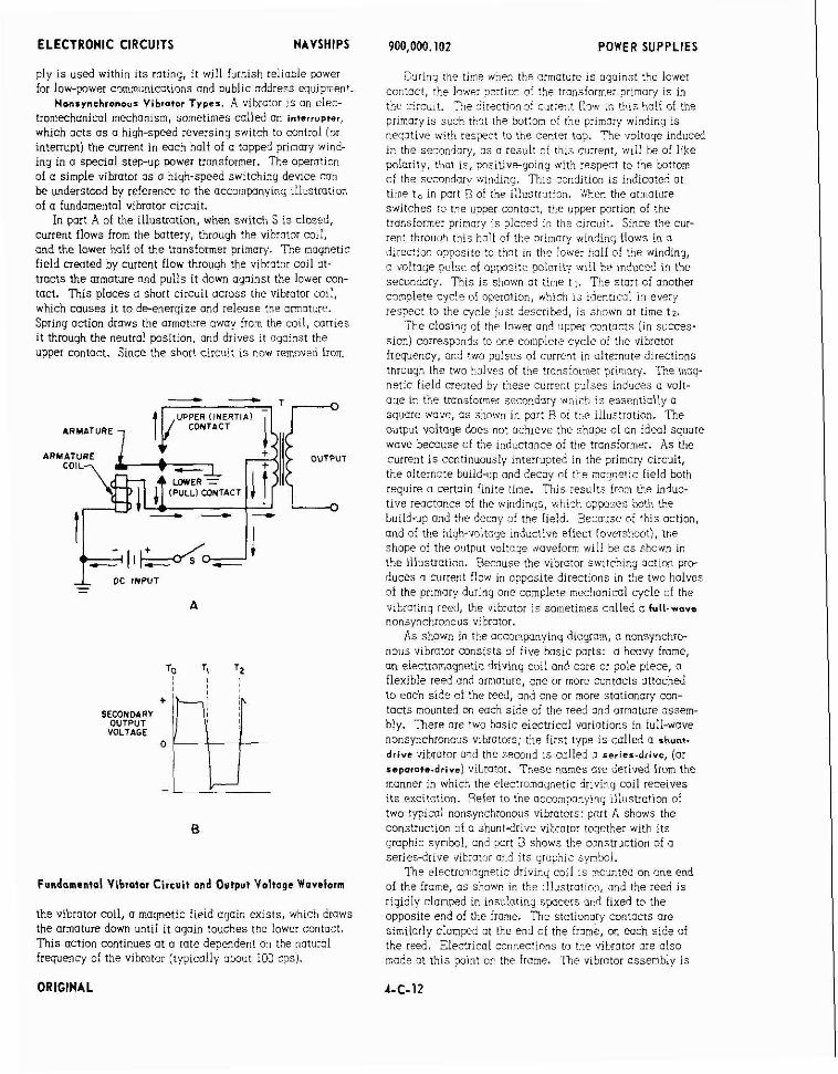
ELECTRONIC CIRCUITS NAVSHIPS
olv is used within its ratina. it will furnish reliotle power . . -. for low-power communications and public address equipment.
Nonsynchronous Vibrotor Types. A vibrotor ;S on elec- tromechanical mechonlsm, sometimes called an interrupter,
which acts a s a high-speed reversing switch to control iqr interrupt) the current in eoch half of a tapped primary wind- ing in a special step-up power transformer. The operoticn of a simple vibrotor as a high-speed switchiny device can be understwd by referencc to the accompanying rllustrntion of a fundamental vibrotor circuit.
In part A of the illustration, when switch S is closed, current flows from the battery, through the vibrotnr mil. and the lower half of the tronsiomer primary. R e mognetic field created by current flow throuyh the vibrntoi coil ot- tracts the armature and pulls it dawn oqoinst the lower con- tact. This places a short circuit across the vibrator coil. which causes it to de-energize and release the omotu;?. Spring action draws the armature away from the mil, corries it through the neutral position, ond drives it oqoinst the upper contact. Since the short circuit 1s now removed from
- - l a , - - I
ARMATURE 7 OUTPUT
Fundamental Vibrator Circuit ond Output Voltage Woveform
the vibrator coil, a magnetic field ayoin exists, which draws the armature down until it agoin touches the lower contoct. This action continues at a rote dependent on the noturol frqdency of the vibrator (typically stout 100 cps).
900,OW. 102 POWER SUPPLIES
T :,9riny the t l re wler the crmolure i s 0gain51 tile lower contoct, the 1'3.~er 301!101 of the Ironsforme: ?rimory is in the c!;cu~t. T>e direction 31 c~~rrent f!3w ir. t5i5 h3U of the primary is such t b ~ t the bottom of the primary ,windin3 is neqztive wit!, reswct to tile center top. Ttle voltoqe induced in the secondary, as o result cf this current, will be of like polarity, thot is, psilive-qolng with respect to the tottom of the secandaiy wlndinr;. Th:s condition is indicated at time I, in port Y of the illustrotian. '{then the armature switches to the uoper caqtoct, the upper portion of the transformer primary is pIoce3 in the circuit. Since the cur- rent thouqil Ibis h d f cf ti.? 3rimory win4iilq flows io o '3;rec:ion o?wsite :o tho1 ir, the lower bolt of the winding, a voltage pclse of apposite polarit" .nil be induced in the secondary. This is shown at time 1:. The sto:t of another csmplete cycle oi operation, which is Identic~i i n eve? respect to the q c l e ;dst described, is srlown at time 12.
The closing of the lw~er and upper antocts (in succes- sion) coirespands to one complete cycle of the vibrotor frequency, and rrro pulses of currelt in alternote dliections throuqi, the two islvcs of the tionsforrner primary. The msq- netic field neated by these cur:ert p ~ l s e s indwes o volt- aqe in the transformer secondary .wLllch is esscnti3liy a sqllare wave, 3s s'lnwn i n part B o! tb,e illostrotion. n e output voltage does not odieve the snope of on ideal square wave bemuse of t5e inductonce of the transformer. As the current i s continuously interrupted in the primary circuit, the a l tern~te build-up ond decoy of the narrretii fleld both require o certain finite lime. This results from the induc- tive reactance of the windinrp, ..ihici. opposes both the build-up ond the decov of the field. Because of this action, and of the high-vnltnqe inductive effect lovershoo:), the shape of the output voIt,:?e - ~ ~ v e f o ~ m wili be as shown ir t'le illusnotion. aecsuse the vibrator switching action pro- duces o current flow in opposite directions in the two halves of the primary during one complete mecilonicol cjcle of the vibrctino reed, the vibrator is sometimes cniled a fu l l -wave
nonsynchronous vibrator. As shown in the occompanyinq diaqran, a nansynchro-
nous vibrator consists of five b s i c ports: a heavy frame, an electiomagnetic driving coil ond core or pole piece, a flexible reed and armature, one or more contacts attached to eoch side of the reed, and one or more stationary con- tocts mounted on each side of the reed and armature ossem- bly. There ore two basic electricnl voriotions in full-wove nonsynchronous vibrators; the first type is called a shunt-
drive vibrator old the second 15 colled a series-drive, (or rspsrots-drivc) vibrator. These names are derived from the manner in which the electromat~netic driving coil receives its excitation. Refer to the occomponying illustration of two typical nonsynchronous vibrators: purt A shows the construction ol a shuntdrive vibrator taqether with its yraphic symbol, and port B shows the construction of o series-drive vibrtor ond its yrcpiic syi.bal.
The electromagnet~c drivinq coil is mounted on one end of the frame, a s show in the illustration, md the reed i s rigidly clamped in insulntinq spacers 2nd fixed to the opposite end of the frame. The stotianory contacts ore similarly clomped at the end of the frome, on mch side of the reed. Elec!iical connections to the vibrator sre 3lso mode 31 this point an 1b.e frame. lhe vibrator assembly is
ORIGINAL
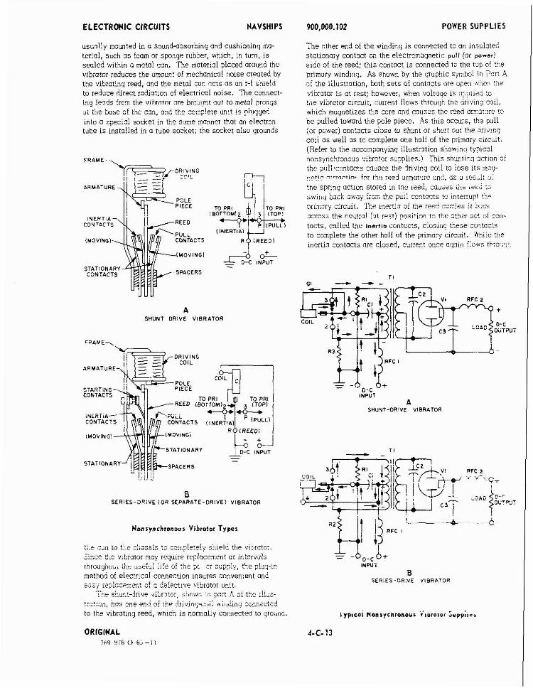
ELECTRONIC CIRCUITS NAYSHIPS
usually mounted in a soundilbsarbing and cushioning ma- teriol, such a s foom or sponge rubber, which, in turn, is sealed within a metal can. The mnteriol placed around the vibrator reduces the ornount of mechonicol noise created by the vitronng reed, asd the metal con ncts as an 1-1 shield to reduce direct radiotion of electiical noise. The connect- is.: ! e l l s finm the vihrntoi ore brought out to metal pionqs ot i t e base of th: con, and the complete un?! 1s piilqqt-4 into o zpecio! socket in the same manner that on electron tube i s installed in a tube socket; the socket also grounds
PIECE , , , ,
CONTACTS
A SHUNT D R I V E VIERATOR
FRAME- . .
STATIONARY -
S T A T I O N A R Y 2 -
i , , , , , " B
SERiES-JP!VE ( O R SEPARATE-DRIVE! VIBRATOR
ti,? c jn to the chassis to c?r,p!e:e!y shie!d the vibrator. .. 2:nct :he vltralar may require replacenlent a1 interviils miwghu. :, i i '- - r .i- -. . ?.."",.. *LO ,4,.. ..,* " t .r,e U>",.,, ,,I= "t L,>= *L ,., ?,,, ~,,. ?.", ... method 01 electrical connection Insures canvenlent and t;si iep:a::xmt S! 3 ?e!ect:.de vibrotor i i~i t .
-. -- .;.."l-iri,.. ~:i..~!,:,~, ;h;,r;, in A O! the . ... . . !:c::c,?, 22s c . ~ e e k ci !+ ~ i r i v ! ~ c ~ ~ : c ~ i ~ w i ~ ~ ? i i q cmr,zcte i to the vibrating reed, wnicn i s normoiiy connectea to groum.
900,000.102 POWER SUPPLIES I The other end of the winding i s connected to an insulated stationary mntoct on the electromagnetic pull (or power)
side of the reed; this contoct is connected to the top 01 the primory winding. As shown by the qraph~c spbo! i n ?31t .4 of the illustration, b t h sets of contocts are open *ncn !'re vibr3toi i s ct rest: however, when voltage i s ii;li;izc to tne vibrator c~icuit, current flows through tne 5rlvin.: coil, which muynetizes t!le core an3 causcs the reed armomre rc be pulled toward the pole piece. As this occurs, the pull (or power) contacts close to shunt or short out !he anvlnr; cod a s well as to complete one half 01 the primary circuit. (Refer to the occompanying illustration show~nrj typic01 nonsynchr3nous vibrator supplies.) This shunting actlon o: :he ;rul!.contacts coiises the lriviny coil to lose its mau- not i r ~~~ nttrort inn inr f?e reed oimoture and, ris o r t s ~ l ; a l the sprlng octlon store6 in tne reei, cuuacs l i ~ L Z ~ Y ;G swiriq h i k znoy {;om the pu!! co:to~ts 1s intnrrllpt !h*
prinrury circuit. The iwrim oi r'le reed czcries : t !>:~c.v
3rrcs5 the ?e?trn! [nt rest! " s i t i o n lo the other set ot con- tacts, coiled the inertio contacts, ciasing these contocts to complete the other hall of the primary circuit. While tne inertia contacts are closed, ?went once ogoin !lows tb,ra;~,::r
T I
+ D - C
INPUT A
SHUNT-DRIVE VIBRATOR
A - -A0.,B+ INPUT
B SERIES-DRIVE V I B R A T O R
ORIGINAL ih9-978 0 - b j - I !
ELECTRONIC CIRCUITS NAVSHlPS
the driving coil and muses a high magnetic attraction to be imported to the reed ma tu re . As the reed moves away from the inertia contacts, these cortocts open to interrupt the primary circuit. The cycle i s then repeated as the r e ~ d i s curried ocross the neutrol (at rest) position to close the pull contacts and once again shunt the driving coil. It should be noted at this time that the peak voltage applidd to the driving coil, during the time the inertia contacts are closed, i s approximately twice the volue of the normal d-c input voltoge to the supply; this i s bemuse the voltage induced by autotransformer action in the half of the primary winding which i s connected to the stationary pull contoct i s in series with the d c input voltoge.
By referring to the diagram of the shuntdrive vibrotor, it will be seen that when the armature i s in the neutrol position (all contacts open), a complete series circuit exists from the negctive side of the input source, through the driving coil and pull winding, to the positive side of the d-c source. For a given value of current, a s determined by the total resistance iri the circuit, the portion of the input voltoge that will be dropped across each of the two circuit elements will be in direct proportion to the resistance p i e sent in each element. Since the transformer orimatv wind- ing offers only negligible resistance to the comparatively small and steady di. cwrent which flows under the con- ditions stated, no appreciable voltoge will be developed across the pull windinq.
When the inertia contacts are closed, the series circuit throuqh the drivinq coil and pull windinq remains completed. The voltage existing across the pull winding and the volt- aqe developed in the inertio windinq have opposite polori-
~ ~
ties. Through the autotronsformer action which tokes place across the tapped primary, the rapidly changing mav netic field oround the inertio windinq induces a voltoge in the pull windinq; this voltoge has the same polarity a s that of the inertio winding. As a result, the voltoge now p r e sent ocross the pull winding will be the difference between the induced voltage and the existing voltoge. Since the induced voltage has the qeater value, the polority of the difference voltage will be the same a s that of the induced voltage. Thus, not only i s the counteracting effect of an apwsinu voltaae neutralized. but the voltaae in the inertia windingis eff&ively aided.'
The seriesdrive (or separate-drive) vibrotor, shown in part B of both illustrotions (the Nonsynchronous Vibrator Types and the Twicol Nonsvnchranous Vibrotor Suoolies). .. .. differs from the ;huntdrive ;ibrator just described in that it has an extra pair of contacts. l l e s e contacts, called smninp contacts, ore normally closed when the vibrator i s at rest. The moving cmtact of this pair is mounted on the armature reed, which i s normolly connected to yround. Tne stationary starting contact i s wired to m e end of the driving call. The other end of the coil i s connected to the high side of the d-c Input voltage sgurce, through a terminal in the base of the vibrator provided for this purpose. As shown in port B of both illustrations, both the inertio contocts ond pull cmtacts are open when the vibrotor i s at rest. How- ever, when wltage i s applied to the vibrotor circuit, cur- rent flows through the driving coil and causes the reed armature to be attracted to the pole piece (magnetized care): thus, the moving pull contact i s drawn ogai,nst the
ORIGINAL
900.W0.102 POWER SUPPLIES
stationary pull contoct. The clasing of these mntacts completes a circuit through one half of the tmnsformer pri- mary. The armature, in moving toward the pole piece, opens the starter contacts, which prevents any further current flow in the driving coil; this results ul the collapse of the magnetic field. ?he reed, now no longer attracted by the pole piece, swings back from the driving mil; this opens the oull mntacts and interrupts the primarv circuit. The inertia of the reed carries it back across the neutral (at rest) position to the inertia contocts, closing these contacts to complete the other half of the primary clrcuit. At the same time, the starting contacts close and current once again flows through the driving coil to produce o magnetic attrac- tion for the reed armature. As the reed moves away from the inertio contacts, these contocts open to interrupt the pri- mary circuit; at the same time the starting contacts open to interrupt the circuit to the driving coil. The cycle i s then repeated a s the reed is carried across the neutral (at rest) position to close the pull contocts ond once again complete the primary circuit. It should be noted at this time that if the seriesdrive vibrotor i s connected in the circuit so that the driving coil receives voltoge directly from the input source (throuuh a seporate contoct in the vibrator base), the vibrator will continue to vibrate mechani- mUy, even though the transformer center tap and end leads are open. This will not occur with the shuntdrive vibrator since the current to energize the driving coil must pass through one half of the primary winding.
In both the shuntdrive vibrotor and the seriesdrive vibrator the current i s alternately switched though each half of the transformer primory, and, as a result of these alternote pulses and the magnetic field they produce in transformer T1, o stepped-up voltage i s induced in the transformer secondary. The resulting secondary voltoge is essentially square in waveform, ond i s applied to the tull- wave rectifier circuit. In the circuits illustrated by the dia- ymms of typical nonsynchronous vibrator supplies, t ranr former T1 has a center- to~~ed secondorv windina: wch end . . -. terminal of the secondary i s connected to a plate of the electron tube. V1. On alternate holf-~vcles of the secund- ary voltage, &ernate diodes of the fuil-wove rectifier con- duct and produce an output voltage across the lwd resist- ance. Since only one diode conducts at any instant of time, electrons flow through the lwd resistance in pulses to prw duce o pulsating output voltoge. The output of the recti- fier circuit i s connected to o suitable filter circuit to smwth out the dc for use in the load circuit; because a square- wove voltage is applied to the rectifier circuit, ond because the frequency of vibrator switching i s fairly high (usually 100 to 120 cycles), very little filtering is rwuired to obtoin a d-c output voltage which i s free from voltage transients and relatively free from ripple.
~ ~
In proctice, the nonsynchronous vibrotor i s normally constructed with a four-pronq Lose, and the socket into which the vibrotor is plugged i s wired to accept either o shuntdrive or o series-dri.e vibrator; therefore, the two vibrator types moy be used interchangeably in o large num- ber of vibrator-type supplies.
Circuit Operation. Both supplies shown in the Non- synchronous Vibrotor Supplies illustration utilize a full- wove rectifier circuit to obtain high-voltage output. ' b e
4-C-14
ELECTRONIC CIRCUITS NAVSHIPS
discussion which follows is concerned primarily wlth the vibrator and its associated tiar.sformer, since the ope:S:ion of a full-wove rectifier clrcuit has been described under Power Supply Circuits, in Section 4. Pa11 h (Singie Phose Full-'hiave Rectifier) of the handbook. Further-:ore, the nonsynchiono~s viir~tor-type p w r r .;;;.dy 1s !lot n.eiessaii!y restricted to the use of a full-wove rectifier circuit lin.3, in mnny i"sronces, the rectifier circuit is iikilr to be G bridqc or voltaqe-doubler circuit employing either e1ectroi.-lube ar semiconductor diodes 35 rectifiers.
Vibrator G1 in the circuit of part A is a si,unt-drive vibrotor; vibrator Gl in the cirmit of pcr! P i s 2 series- drive vibratr,i. Traisfoiaer T i , in joth circuiis, is ,J icecioi power tronsfarmer s:!'. 3 ce?!e!-:c"pe? ?r?!mrj l r 4 iav!ei- +,""'A cPmn,inri, iquFvr- . ' ? "r.4.;. -. .:>it :.:e. ~,,"I.i91 .-Fr.-..-... ~ ~ , ,
rectiiier circuit is osed instead or a tuil-wave recililrr shown, the trari~foia~er seioiiLaii. is?? iz: b t cez:e:-tznced. . . Elect:an iu'w 'v'i :s a twirl-,ilodi reztl;,-3:, 3:7 X:Y be ei:::~: s n i-,4i:ec!iv hmte? c?!ho?e r~ctifiiir li o rps-filled ~016- cothode rectifier. Bypass capacitor C1 ond r-f ii.oKe RFCi serve as a filter to eliminote or reduce impulse electrical noise (or "hash"), arijinoted by o:cirt; vlbrotili cs.tsc:i, from beino rodiated bv the 3-c inwt leads and coiaied ;n:o other circuits oi the equipmenr. ?,*s:sv.>rs Ri i l ; i . 7.2 ;re connected ocross the i"terr~piei cnnt,7c:s ilf :t,e ~.iSilta: to reduce interference and sparkinu m.3 uiso t i ;c8i:ec;e :kz l ife of the vibrator contacts: the value of R1 and R2 i s usually between 47 and 22C ohms, dependinq upon the d-c inout voltooe and circuit desion. Fiesistors R l and 32 oiso help to reduce the peok amplitude of any trarisient voltayes which -,, -< ....g ht OCCUI !n the ni:mnrv r!rrulr <>enruse oi vthmcor
switchinq action. Copaciter C2; commonly col!ed the buffer n r , ,.' L,<t,!, "nd ,JL,, ,~5i~;,zll" -.:'?;::< :? :: :>,: ?::?:: 2: !!?;
ing copxcitor, is connected a~ . ros i the !:?isij:~~r : F , ~ ~ P ^ .
arv to effectively absorb the nlqh translent voiroi~es produced by the inductive reactance when the primary current is inter- rupted by !he opnifilj ?: the i-iL:;:,;; ;sr.:;ctr. Dec?:zc cf the magnitude of these voitoyes, it 1s necessary mat <ne buiier capacitor nave o rating in wuikirlq volts of i r m 6 t; P times thp unltoge delivered bv the Dower sup~lv. For example, for a supp!y which delivers 250 volts the capaci- to: s';cu!?. be r3!04 bt.t.Nee. l ion 0.i ?cliin ,workin<! volts. $1 resistor of ooproiiimatelv 509C oiims 1% soretmes mn- nec:ed in series with the kmifer cn:nclti,r to ;i!li~t t n r w r r t r . ; ~
-...o-. in -.in +Lo h.,f'mr ?~l,"rjtn~ i r r n r n ~ s shnrt-,i. "., -" ....,. ... ---. . -- ..-) - - z - L ." """",*". <l*ma"A" ,,m" ,,~,* ,-iFr,,;, :::c w.i,..- .?? ., ..,?i ^".i.n.,;r; ....... &;>.> (t:3<s:a:r.s7 ;:.::,: :7t:c z-.? z!!:c:.!? !",e,,r.-"r-
. . ,$ibrstrrr fie79eno: ,,..-,, = t - ! i.i -... :- ....,I. . . 1 . i . 8 . . - ..7.--" . . r : , ,>r, 2
.;47 ,d, Capacitc,?~ asei i?, :!.;s :;;Lz?!::? ;e?e!?'.:; .??,!?
3 bregkdcwn vc!!q7e nf In00 tn )!I00 volts. Tn ;OF? i i i i l i t j - LLf'"? ....?? -;*-. ," "-" ,,--,-" qr,-<c .?,? .r-n<,,:: ..,or
~ ... ~ ~
maw. ,?,;r::lt .;-.r:?*icr ::;?s !b - ?r i t? r r,lr.,,-lrnis . . .~ - ~ ot q u a i " " L L , ~ , d i""*Liil,i .s "".,.,L i.-.- i. . - . . _ . ,. sern.dcry to .;rolmd nr tc tne C P C O ~ ~ T , , - : Y ' I I ~ # it^:,. D V D ~ S S
;:t~paci!cr 3 ornil: r-! cF.oke 3?72 !nr: 7- '.'!!::?n-! i!!?r :s ?:r:c?,t zcise (c! ''hc<b''] h r n w r c q m,f"ie< TO miter circuits throuyh the hiin-uniraye, d-F miput i d .
',When 1-c inn:it ?n.ser is (1~0iie3 IC ~ : : e i . ! i ~ , ~ i l , i,,e d i ld - :-.. -*:, -* .,:, .-q,*. ,:., --- ," c.,7r, ,-- ,*-,: " ,.,, <,;. .,,,,-" ..-... "." . ~ ~ ~
i t> ,+ s t i ts G~;+z G Z : ; ; ~ ! ~ C < ~ C : C ; . :! be Cp%"!!rn!! "! G"l7"T-
dr~ve una series-dr~d? ' $ L C T G L , X ~ * ,.., uz u..," :- ... :..>.~
900.W0.102 POWER SUPPLIES
able detail in previous paragraphs; therefore, a description of vibrotor switching action will not be repeated here.)
FAILURE ANALYSIS. G.ner.1. A quick check to determine whether the vi-
brator i s operating i s to listen ior the chnrocteristic m s i r oilicd b~zzing noise which is mode by the vibratinq anion 6: the reed cssemoiy: oi<nougn < ~ e red osses~~ily ia ri!- closed in a sealed con and is cushioned to deaden the sound, on audible indication con usuoiiy be detected. How- ever, this simple check is not o positive indication of mr- rect vibrator operotion: for example, the seriesdrive vi- b;.~tor vill chen mntime to operote even when there are discontinuities in t ie tronsformer primary circuit.
Tile most frraoent trouble which develops in a vibrator- . . . . , ~ - ~ d . - -- .--....- ..<k.".". m." &<-*i,." 'ypC bwpp', ,a IYY>c" "I > I,.. L ..-. ".-. -. __
bs!fer ccpi.ci!oi 7 i e powpi tronsformer and the rectifier- -.,-.,it ccmmrieoii ;eneriiiy i i i v i a iisefui !ife which i s coxoarobie to the hie of the components in a mr~ventionul power supply desijned lor o i input.
Although certain wavetorm measurements can k mode w!th an osci!lascope to check for correct operation of the vibrator supply. this teciuique will not always immedimely .=veal troobles within the supp!y, since mechwical defects ,v:hicb, mw be of short duration sometimes occur only after .L- ...- ,.;L.* ..,..13: rexc"es c certain onerating temperature.
An indication of vibrotor owrotion con be quicklv ob- . . tained by using an oscilloscope to observe the voltoge wave- form at the primav of the power transformer. If measure- ments me made at each end oi the primary to chassis ;iiround;, ;ar 2*n.;i-;i& ;zj;i;ujc oi ii;; ; Y e will be approximately equni to twlce the value of the d s in- nut vnitonp. hnw~ver. if the oscilloscope vertical input i s ;.ornenP? across thr eltire m-7ry winding, the peok-to- peak miplituda of the sqxre wi.95 wii! be approximste!,; equol to :mi rimes the vaiue of the d c input voitoge. When the vibrator circuit is oppraring normally, o square wove *ill be obsewid with re!aii;.ely snoc:' bonsiticn ociiliring cfte: the contons break and during the voltage reversal when another set of contacts make to produce the next ho l fqc le of the woveform. The flat portion ot the square wave should be relatively smooth; if radicai tran- sients npperlr on the fiat wnion of tne square wove, this i s on indicution oi pmi eleniicai iontoct, cxsea by chat- terinn or houncino of the mntacts, and i s o good reason to SIIS???~ thot the vibrator i s defective. Mlnor muohness, or .. . ., . ,.
r l r , ? # r on i r ~ r r i r i i :roiilurl u; Ljs ;suuit n ~ i t is i.G: ; s ~ .. .. ,C3!i'+ 7 d l l l C l ~ " ~ COkjSe k b L ~ . ; z L ~ I!!: v i b ~ ~ t ~ i , S ~ ? I C ~ tk2& i;- ?!T?tIO" -ere,y ,*?WSP,~IS SGE? s:,,";: 4&,gl;~r, ic c G ~ : ~ z
Teslstance during tne time the vibiatni cunlacls are c losd. , I t = sm,Ld,tr,r,ess c,; I;,- ,:c:,sii.";, ..".., a;,* :.c:-:>;p2: >,,-
tion of the sqmre wave, thitujh !he voltage r e v e r s ~ ~ (mn- '--.- --.- .- ..- ..,--. ,~,,.: ..,,,.. ... ; <-,,- f ::,- .; ,,,,, Te . . .~ ~ -..., , , ~ . ~ . . , . +G.*e 15 cG;:railE p; ::;e,/~:&e L! i::ei,uff*r (&7LLr>g;, <,>Z,? . .
-i*lr. the indl~ctiva reactance of the !ronsfoimer, the nat- ural hwencv of the vibroior reed assembly, and <he e a s t , , ,e i ,e>..een +,.. mntnct c!os!lres.
.,ZL ,t,,en the jixp!ci;.s onkc'.ckc. :r.?icc!e !'.at !he v:-
ORIGINAL
ELECTRONIC CIRCUITS NAVSHIPS
operating characteristics; therefore, the replacement vi- brator should be the same type us the original, or at least o vibrator which i s recommended by the manufacturer a s the correct replacement for the original.
No Output. The nonsynchronous vibrator supply con- s is ts of a vibrator and associated transformer, and a recti- fiet and filter circuit. Therefore, when checking the vibra- tor supply for a possible defect, tests must be made to determine whether the trouble i s due to a defective vibrotor and associated t r~s fo rmer , or to o defect within the recti- fier circuit.
The d s input voltage should be checked to determine whether it i s present and of the correct value.
The operaiion of the vibrotor can be checked by an a c voltage measurement made at the secondary terminals of the transformer, or by use of on oscilloscope connected to the primary circuit to observe the switchinq-action waveform. If the "ibrator ond associated transformer are found to be functioninq normally, a s indicated by o semndary-voltaqe measurem.&t or an oscilloscope c k c k , it must be assumed that the trouble i s in the rectifier circuit or the associated load. A check of the rectifier circuit can be made in ac- cordance with the procedures outlined in Section 4, Port A for the applicable rectifier circuit: in the case of this portic- ulor vibrator-supply circuit, reference should be mode to the Sinpl..Phase Full-Wav. rectifier circuit. If the vibrotor- type power supply blows its d-c input fuse each time the supply i s energized, the vibrator muy be defective. To eliminate this possibility, remove the vibrotor and substitute another vibrator of the some type in i ts place. Then install a new fuse and apply power; if the fuse does not blow and operotion appears to be normal, the original vibrotor must be considered defective. However, if the fuse blows again, the original vibrotor may be considered good, md further checks of the supply will be necessary in order to locate the source of the trouble. When burned or pi* -d vibrotor contacts stick together, a heavy current flows in the as- sociated primary winding, and this current i s likely to blow the fuse. A check of the input current should be made with on ammeter to determine whether this current is within tolerance, or whether it i s excessive. With the vibrator r e moved from its socket, continuity measurements of the transformer primory circuit may be made to determine whether the primary winding isopen, shorted, or grounded. Again a known qmd vibrator may be substituted for the suspected vibrotor to determine whether the vibrotor i s one possible cause of improper operation. Also, removal of the rectifier tube, as applicable will indicate whether the trouble i s in the vibrotor, or in the rectifier or lwd section of the supply.
A shorted buffer copocitor C2 can be detected by a higher than normal input current to the supply and a very low a s voltage a t the secondary terminalsof the transfor- mer. The replacement buffer copacitor should be the same value a s the original capacitor and of equal or greater volt- age rating. A lwky or shorted filter capacitor C1 will also cause the input current to thesupply to be above normol. As a general rule, any time the vibrotor i s replaced the buffer capacitor should also be replaced.
The indirectly heated cathode rectifier, V1, i s frequent- ly subject tc heater-tocathode leakaqe, and, since the
900,000.102 POWER SUPPLIES
heater i s normally at ground potential, this leakage will cause an abnormal load on the rectifier output: a complete short will result in no d s output from the supply. Also, o short in filter copacitor C3 or on open r-f choke RFC2 will result in no output from the power supply.
L ~ w Output. A Iow-autput condition in a nonsynch- ronous vibrator-type power supply usually results from a defective vibrator, a leaky buffer capacitor, low input wl t - age, or a defective component in the rectifier or filter cir- cuit.
A voltoge drop in the primary leads to the supply con result in lowoutput; therefore, the input voltage should be checked at the transformer or vibrator terminals to deter- mine whether the input voltage i s present and of the cor- rect value.
The a c secondary voltage may be measured at the transformer to determine whether it i s approximately the value specified for normol operation of the supply. The test procedures described for the noautput condition and in previous paragraphs can be used to determine whether the vibrotor i s at fault. A defective vibrator with only one set of properly making contacts results in reduced output from the supply. A vibrator in which "frequency hunting'' oc- curs moy be detected by an uneven or irregular buzzing noise, which indicates that the armature i s vibrating er- ratically and a t frequencies other than its normal frequency of vibration. This unstable condition of the vibrator causes the stepped-up voltage induced in thesecondary of the tronsiormer to also be erratic, and the output voltage to be below its normol value. This trouble i s usually caused by excessive loud current, and isan indication of impending vibrator foiiure. Frequency hunting con also be caused by burned or pitted vibrator contacts which are sticking; this usually results in a higher than normal input cutrent and reduced output from the supply. A check of the input cur- rent shoiild be made with an ammeter to determine whether the current i s within tolerance; also, on oscillosmpe check of the waveform at the primary of the transformer should be made to determine whether thevibrator i s faulty. If desired, a known good vibrator may be substituted for the suspected vibrator a s a quick check to determine whether the vibrotor i s actually at fault. A check with the rectifier tube r e moved isalso recommended. Shorts, leakage, or excessive current drain in the filter circuit or in the high-voltoge load circuit external to the supply will cause a heavy loud on the vibrotor contacts, ond may cause early failure of the vibrotor. The output lwd current should be measured after installation of a replacement vibrator to determine whether the load current i s within tolerance; if the load current i s excessive, the replacement vibrator may be damaged unless the cause far the excessive Icad current i s found and F r - rected.
Continuity mmsurements oi the primary md secondary windings of transformer TI should be made, since an open circuit in either of the windings will cause a reduction in output.
The rectifier, V1, may be weak and cause low output. The tube i s usually an indirectly heated cathode type, such a s a type 6x5, 6x4, or 12x4, or a gaseous rectifier, such 0s a type 024. In either case, a quick check of rectifier condition can be made by s~ubstituting a rectifier know to
ORIGINAL
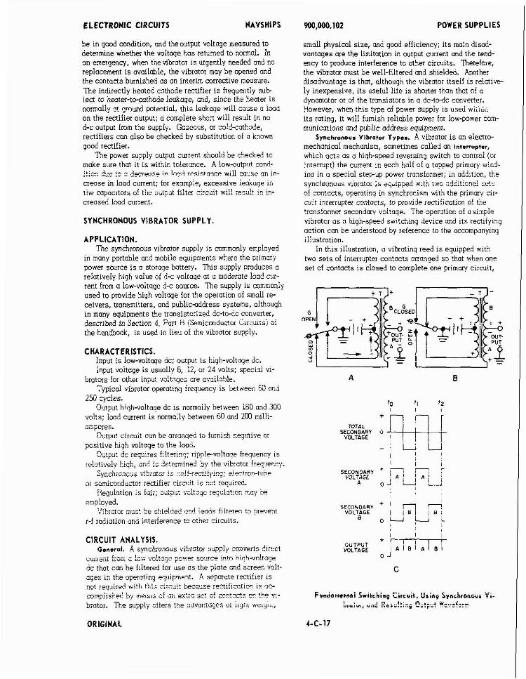
ELECTRONIC CIRCUITS NAVSHIPS
be in gmd mndition, and theoutput voltage measwed to determine whether the voltage has returned to normal. In on emergency, when thevibrotor i s urgently needed ond no replacement i s wailable, the vibrator may be opened and the contans burnished as an interim corrective measure. The indirecdy heated cothode rectifier i s frequently s u b i en to heater-tozothode leakage, md, since the heater i s normally m ilrnund ontentiol. this leakaoe will cause o imd . - on the rectifier output; a complete short will result in no d-c output from the supply. Casmus, or coldiothode, rectifiers con alsa be checked by substitution of o known good rectifier.
The power supply output current should be checked to make sure that it i s within tolerance. A low+utput cond- a'-- A,... " A---., in lnnd r~+istnnct? will muse on in- ... u.. -"- ." - ~~~
crease in load current; for exampie, excessive i d a g e in the capacitors of the outpiit filter circuit wi!! resdt i- ir.- creased load current.
SYNCHRONOUS VIBRATOR SUPPLY.
APPLICATION. ?he synchronous vibiotor supply i s mmmonly emplayed
in many portoble and mobile equipments where the primary power source i s o storage battery. This supply produces a relatively high value of d-c voltoge ot a moderate load cur- rent from a low-voltage d-c source. The supply is mmmonly used to provide high voltage for the operation of small re- ceivers, transmitters, and public-oddress systems, although in many equipments the transistorized dc-lo-dc converter, described in Sectlon 4, Part ii (Semicmductor i ic i i i t s ; oi the handbook, i s used in lieu of the vibrator supply.
CHARACTERISTICS. Input i s low-voltage dc; output i s high-voltage dc. Input voltage i s usually 6. 12, or 24 volts: special vi-
brators for other input voltnges ore avoilohle. Typical vibrator operating frequency i s between 60 and
250 cycles. Olutp~ut high-voltage dc i s normally between 180 and 300
volts: Imd current i s normally between 60 and 2m milli- mperes.
Output circuit can be arronqed to furnish ngative or positive high voltage to the load.
Output dc requires !il!eric:: ripplevoltoge frequencv is :elu!ivr:y high, ;;d i s detc-ined bi the vibrntor fieqlenry.
Synchronous vi.lbrs?or i s .?elf-recti!ying: eiec!ran-tiine or semiconductor rectifier circuit i s not reqmred.
Rgulotion i s fair; output val:aqe rqda!:or. moy De emploved.
Vibrotor must be s'h~elbed a d ieadc f~i terw to :>revent r-f rodiotion and interference to other circuits.
CIRCUIT ANALYSIS. Cenerol. A synchronous vibrator supply converts direct - . L--- - I-... ..-I.--- --,.,.v e n , , r r e intn hilhvnlfaoe LUile,,, L i U L S , " ."" ."..",,- yu.. -. .~~~
dc that can be filtered for use a s the plate and screen volt- ages ir, the operating eqiiipment. A sepnrote rectifier i s z-t require,? with this circui! because rect;ii3rion is ac- coinpiished hy innims of zn e a i x jet of CC~!X!C 0" t" 711-
brator. The suppiy alters the oovantages o; iig;,i ntij;...
W0.000.102 POWER SUPPLIES
small physical size, and good efficiency; i ts main disod- vantages are the limitation in output current ond the tend- ency to produce interference to other circuits. Therefore, the vibrotor must be well-filtered ond shielded. Another disadvantaqe i s that, although the vibrator itself is relative- ly inexpensive, i ts useful life i s shorter than that of o dynamotor or of the transistors in a d c - t d c converter. However, when this type of power suppiy is used wiiiliil i ts rating, it will furnish reliable power far low-power mm- munimions and public address equipmenr.
Synchronous Vlbrmtor Type.. A vibrotor i s on eiectr(r mechaniml mechanism, sometimes called an interrupter,
which acts a s o high-speed reversing switch to control (or interrupt) the current in each holf of a topped piimory wind- inn in a special step-up power transformer; in oddition, the synchronous vibrator ;s eqiipped wit' a, '. ,+,- - u-u~c..,..L. -*""---I --+- --.- o! contacts, operating in synchronism with the primarv nr- N i t interrupter contacts, to provide rectification of the transformer secondorv voltoqe. The operation of o simple vibrotor os a high-speed switching device and its rect~iy~ng action con be understood by reference to the acmmponying illustrotion.
In this illustration, o vibrating reed i s equipped with two sets of interrupter contacts arranged so that when one set of contacts i s closed to complete one primary circuit,
I
VOLTAGE 0
Fwdamernai Switching Circuit, i i r inp S y n i b r ~ n c - i V i 3 . o ir-..n .~.~.i..- "I",",, U.," ..-.. ..... " -" .?-.
ORIGINAL
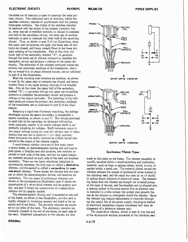
ELECTRONIC CIRCUITS NAVSHIPS
the other set of contacts i s open to interrupt the other pri- mary circuit. Two additional sets of contacts, mlled the r.ctif1.r contacts, operate in synchronism with the primary interrupter contacts. The action of the rectifier contocts i s identical with the action af the primary contacts; that is, when one set of rectifier mntacts i s closed to complete one half of the secondary circuit, the other set of rectifier contacts i s open to interrupt the other half of the secondary circuit. Thus, as shown in w r t A of the illustration. when the uppei sets of contacts are open, the lower sets of con- tacts are closed, and heaw current flows in the lower pri- mary winding of the transformer. Also at this time, the lower half of the secondary, marked "A", i s grounded through the lower set of vibrotor contacts to complete the semndary circuit and produce a voltage at the output ter- minals. The polarities of the voltages produced across the primary and secondary windings of the transformer, which are so wound that no phase reversal occurs, are a s indicated in part A of the illustration.
When the vibrating reed reverses i ts position, as shown in pan B, the upper se ts of cmtacts me closed, and heavy current flows in the upper primary winding of the tiansfor- mer. Also at this time, the upper half of the secondary, marked "B", i s grounded through the upper set of rectifier contacts to complete thesecondory circuit and produce a voltoge at the output terminals. The polarities of the volt- ages produced across the primary and secondary windings of the transformer are as indicated in part Bof the illus- tration.
Assuming a rapid rote of primary switching, the voltage developed onoss the entire secondary i s essentially a square waveform, os shown in purl C. The ita age produced in each half of the secondary on oilemote half-cycles, when combined, results in on output voltage which is es- sentially pulsating d c voltage. Small transiertts occur in the output voltage during the time the vibrator reed is trons- ferring fmm one set of contazts to the other; however, these t ronsims are easily removed by a f~lter circuit con- nected to the output of the vibrator supply.
A synchronous vibrator consists of five basic parts: a heavy frame, an electromagnetic driving coil and core or pole piece, a flexible reed and armature, two contacts at- tached to each side of the reed, and two (or more) stotion- ary contacts mounted on each side of the reed and armatwe assembly. There are two basic electrical variations in synchronous vibrators; the first type i s called a shunt-drive vibrator, and thesecond i s called a sarierdrive (or lapa- rob-drive) vibrotor. These names me derived from the mM-
ner in which the electromagnetic driving coil receives i ts excitation. The two types of sychronous vibrators are shown in the accompanying illustration; part A shows the construction of n shunt-drive vibrator and its graphic sym- bol, and part B shows the construction of a series-drive vibrator and its graphic symbol.
The electromagnetic driving coil i s mounted on one end of the frame, a s shown in the illustration, and the reed i s rigidly clamped in insulating spacers and fixed to the op- posite end of the frame. ?he movable mntacts are mount- ed on the sides of the reed. The stationary contacts me similarly clamped at the end of the frame, on wch side of the reed. Electric01 connections to the vibrator me also
ORIGINAL
A SHUNT DRIVE VIBRATOR
POWER SUPPLIES
DRIVING COIL
POLE PIECE
REED
PULL CONTACTS
SPACERS
B SERIES-DRIVE VIBRATOR
Synchronous Vibrator Types
made at this point on the frame. Tne vibrator assembly i s usually mounted within a soundabsorbing and cushioning material, such as fwm or sponge rubber, which, in turn, i s sealed within a metal can. The material placed mound the vibrator reduces the amount of mechanical noise a w t e d by the vibrating reed, and the metal mn acts a s an r-f shield to reduce direct radiation of electrical noise. The connect- ing leads from the vibrator are brought out to metal prongs at the base of thecan, and thecomplete unit i s plugged into a special socket in thesame manner that an electron tube i s installed in a tube socket; the socket also grounds the can to the chassis to completely shield the vibrator. Since the vibrator may require replacement at intervals through- out the useful life of the power supply, the plug-in method of electrical connection insures convenient and wsy r e placement of o defective vibrator unit.
The shuntdrive vibrator, shown in part A, has one end of the drivirq-coil winding mnnected to the vibrating reed
ELECTRONIC CIRCUITS NAVSHIPS
(normally connected to ground); the othm end of the winding i s mnnected to one of the insulated stationary primary con- tacts on the electromqnetic pull (or power) side of the reed. As shown in part A of the illustration, all mntacts me open when the vibrator i s at rest; however, ,when voltage i s applied to the vibrator circuit through the power trans- fcimei ~srimaru, ;Lye" !!--s tb:ou<h the drivinq coil and ' . couses the reed armature io be pulled towaid the pole piece. As this occurs, one set of primary mntacts, called the pull or power mntads , close to shunt or short out the driving mil and also complete one half of the primary circuit. (An additional set of pull mntocts, called the rectifier contacts, close to complete one half of the secondary circuit at this time.) The shunting action of the primary pull mntocts causes the driving coii to iose ,is mogneric utrruciiuu :fir
the reed m a t u r e and, a s o result of the mechanical energy stored in the reed, causes the reed to swing back away from the pull mntacts to interrupt the primory circuit and oiso break the secondmy circuit. The inertin oi the reed carries it back a n o s s the neiitral (at rest! position to the other set of primary mntacts, called the inertia mntacts, closing these mntocts to complete the other half of the pri- mary circuit. (An additional set of inertia contocts, called the rectifier contacts, close to complete the other half of the secondary circuit at this time.) While the inertia con- t a n s are dosed, current once ogain flows through the driv- ing mil and causes a high magnetic attraction to be impan- ed to the reed armature. As the reed moves away from the inertia contacts, these contacts open to intempt the pri-
-:--4. --A-Ie- h.-L. *h. .~m"n,inrv circuit. The !L!",y r l r r " , , ullurr... " .--. cycle i s then repeated a s the reed i s carried anoss the neutral (at rest) position to close the primary pull mntacts, thus shunting th; driving mil, and also closing the rectifier pull contocts to complete thesecondary circuit. It should be noted at this time that the peak voltage applied to the driving coil, during the time the inertia mntocts are closed, i s approximately twice the value of the normal d-c input voltage to the supply; this i s because the voltage induced by autotransformer action in the half of the primory winding which i s connected to the stationary p d l contact i s in series with the d-c input voltage.
By referring to the diagrm oi the shuni-ddve vibrator, it will be seen that when the armature is in the neutrol position (all mntocts open), a mmplete series circuit ex- i s ts from the nqatlve s ~ i e oi ihe inpur source, through the ir>ving mil and pui: winding, to the ps i t ive s;ie of t e 4 x source. For o given value of current, a s determined by the :ad resistance in the c i r ~ ~ i ! , !he portion of the input volt- age that will be dropped across mch af the two circuit tler,en!s will be ic & r e propcrtiog to the resistance p i e sent in each element. Since the transformer primmy nind- ing offers only nqligible res is tanc~ to the mmparotively smdl and steody d-z current which flows under the mn- ditions stated, no appreciable voltage will be developed across the pull winding.
When f i e lnertla contacis are ciosrii, tile aeiits i i r ;u i i through the driving m i l and pull winding remains completed. The voltoge existing across the pull winding and the valt- zge brve:opij in ibeiilerri; .xi-2:-g have 3ppesi!? M!Z- :iip-. Throlic?h the au:atrms!arne: cc!:on w h ~ h tokes plcce across the tapped primow, the rapidly changing magnetic
900,OM). 102 POWER SUPPLIES
field mound the inertia winding induces a vol tqe in the pull winding; this voltage has thesame polarity a s thot of the inertia winding. As a result, thevoltage now present across the pull winding will be the difference between the induced voltage and the existing voltage. Since the induced vol tqe hos the greatervalue, the polarity of the difference voltone will be thesome a s hot of the induced voltaae. ?,us, s t only is the mmtsncting e!fect 041 on oppasing voltoqe netralized, but the ~ l t a q e in the inertia windinq i s ef&tively aided.
The series-drive (or separate-drive) vibrator, shown in part B, differs irom the shunt-drive vibrator just described in that it has an extra pair of mntacts which are normally closed when the vibrator i s at rest. These mntocts, called . .. - --.- 4- -- :- --.:-- ... i.,. *La mnn&inn .""'DO L Y , , l u r L r , ...... y.-_... ~.~ to one end of the drivinq mil, while the other end of the drivinq mil i s mnnected to the d-c input voitaqe, either through a separate terminal in the vibrator base or to one of ihe stationury primary coniacts. A s show. in the illustra- tion (par! B)* 011 pull and inertio mntacts are open when the vibrator i s at rest; however, when voltage i s applied to the vibrator coil circuit, either through a stationary primory- pull contact or through a separate terminal in the base, current flows through the driving mil and muses the reed armature to be pulled toward the pole piece. ?he reed con- tinues to move toward the pull mntocts and, as the pull mntocts close to mmplete one half of the primory and secondary circuits, the stating mntocts are opened, caus- ing the driving mil to lose i ts magnetic attraction for the r e d nrmoture. The reed now swinis back away from the pull coatocts, because the drivin: mil has lost its magnetic attraction for the reed armature, cnd the pull contacts open to interrupt the primory cnd secondary siicuits. '3.e i;.- enia of the reed carries it back ocross the neutral (at rest) position to the inertio contacts, closing both the primuiy and rectifier contacts to mmplete the other half of the pri- mary and secondary cficuits. At the some time, the start- ing m?!acts close and current once ogain flows through the driving coil to produce a magnetic attraction for the reed imature. As t5.e reed moves awcy from the inertio mn- tacts, the primary and rectifier inertia contacts open to in- ierrupt both circuits; at the s m e "me the s:artin~ m a t o a s apen to interrupt the circuit to the driving coil. The cycle i s then repeated a s the reed i s carried across the neutral iatrest; posihm to LAUS= - t - . .L- ,,.= ruJL - . . I ! .-,. --nlaCtr .- cni once o ~ a i ?
;;:.;lete the prima;; and s e m d ~ r y dicuits. :i sk,o;!2 t a noted at this time that if the series-.drive vibrato; i; cur,- netted in the circuit so tho: the driving mi! receives vol!- q e d i rmly irom the input source (throtqh a separate mn- !wt i" the vihiotor hose), the vibrator will continue to vi- brate n e c h ~ ~ i c u l i y , even t k a & :". :raxfo:mer pri-lory center-tan ond end lmds ore open. ?>is will not wcur with the shuntdrive vibrator, slnce the current to energize the driving mi! must pass through one hol! of the primary wtnd- ing. -
i ne uuipui wluiiiy of a sync>;;n;u~ ':i":*a: F 2 e : Z E p
ply depends upon the polarity of the d-c input voltoge. ?or this reason, means are often providd for reversing the d-c
;?!zity. k :roeice, !he sym-hionous r:biato; i s .. nama!!y m n s t r ~ c d ~ i i h o ~ p e c i o : five-pion* base, on: the special seven-prong socket into which the vlbrator 1s
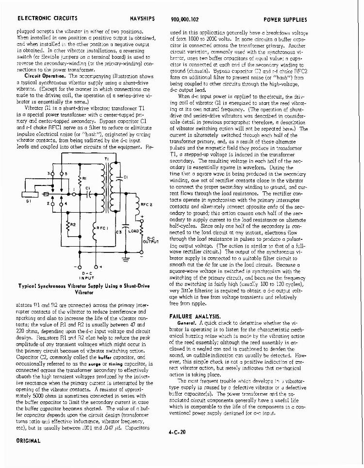
ELECTRONIC CIRCUITS NAVSHIPS
plugged accepts the vibrator in either of two positions. When instolled in one position a positive output i s obtained, and when installed ir the other position a negative output is obtained. In other vibrator installations, o reversing switch !or flexible jumpers an o terminal board) i s used to reverse the secondary-windinq (or the primary-winding) con- nections to the power transformer.
Circuit Operatter,. The occoapanying illustration shows a typical synchronous vibrotor supply using o shunt-drive vibrator. (Except for the manner in which connections are made to the driving mil , the operation of a series-drive vi- brator 1s essentially the same.)
Vibrator G1 i s a shuntdrive vibrator; transformer T1 i s o special pawer tronsformer with o center-topped pri- mary md center-topped secondary. 3yposs capacitor C1 and r-f choke RFCl serve a s a filter to reduce or eliminate impulse electrical noise (or "hash"), originated by arcing vibrator contacts, from being radiated by the d-c inpui lwds and mupled into other circuits of the equipment. Re-
D - C 1 N PUT
Typicql Synchronous Vibrator Supply Using 0 Shunt-Drive Vibrator
sistors R1 and R2 are connected across the primary inter- rupter contacts of the vibrotor to reduce interference and sparking and also to increase the life of the vibrator con- tacts; the value of R1 and R2 i s usually between 47 and 220 ohms, depending upon thed-c input voltoge and circuit design. Res:stors R l and R2 also help to reduce the peak amplitude of any transient voltages which might occur in the primary cirmit becouse of vibrotor switching action. Capacitor C2, commonly colled the buffer capacitor, and occasionollv referred to as the surge or timing capacitor, is . . connected onoss the transformer secondary to effectively cbsorb the hiqh transient voltases produced bv the induct. . ~
ive reactance when the primory current i s interrupted by the opening of the vibrotor contacts. A resistor of oppraxi- mutely 5003 ohms is sometimes connected in series with the buffer copacitor to limit the semndory current in case the buffer capacitor becomes shorted. The value of a buf- fer capacitor depends uwn the circuit design ltransformer turns rotio and effective inductonce, vibrotor freqilenq, etc), but is usually between ,001 and .047 pf. Capacitors
9OO,M)0.102 POWER SUPPLIES
used in this application generally hove a breakdown voltoge of from 1000 to 2OW volts. In some circcits o buffer capo- citor is connected ocross the transformer prirnory. Another circuit variation, commonly used with the synchronous vi- brctor, uses two buffer capacitors o! equal value; a cnpo- citor i s connected at each end of the secondary winding to ground (chassis). Byposs copacitor C3 ond r-f choke RFC2 form an addition01 filter to prevent noise (or "hosh") from being coupled to other circuits through the high-voltage. d-c output leod.
When d x input power i s applied to thecircuit, the driv- ing mil of vibrator G1 is energized to start the r e d vibrot- ing at i ts own natural frequency. (The aperotion of shunt- drive and seriesdrive vibrators was described in cons~der- able detail in previous paragraphs; therefore, a description of vibrator switching action will not be repeated here.) The current i s alternatelv switched throuah each half of the tronsformer primary, md, a s o result of these alternote pulses ond the moqnetic field thev produce in tronsfomei . . T1, a stepped-up voltoge i s induced in the transformer secondary. Tne resultinq voltaqe in eoch half of the sec- ondary i s essentiolly square in waveform. Ihrnng the time thot a square wove i s beina produced in the secondarv . . winding, one set of rectifier contacts close in the vibrator to connect the proper semndory winding to ground, and cur- rent flows through the lood resistance. Tne rectifier con- tacts operate in synchronism with the primary interrupter contacts and alternately connect opposite ends of the sec- ondary to ground; this action causes each half of the sec- ondary to supply current to the load resistance on alternate halfsqcles. Since onlv one half of the secondow is con- nected to the lood circuit at any instant, electrons tiow throuqh the load resistance in pulses to produce o pulsot- ing output voltoge. (The action is similar to that of a full- wave rectifier circuit.) The output of the synchronous vi- brator supply i s mnnected to a suitoble filter circuit to smooth out the dc for use in the load circuit. Becouse a square-wave voltage i s switched i n synchronism with the switching of the primary circuit, and becn~rse the frequenq of the switching i s fairly high (usuolly 100 to 120 c,cles), very little filtering i s required to obtain a d-c output volt- age which is free from voltoge transients and relatively free from ripple.
FAILURE ANALYSIS. General. A quick check to determine whether the vi-
brator i s operating i s to listen for the characteristic mech- anical buzzino noise which i s mode bv the vibiotina anion of the reed os;embly; although the reed assembly i; en- closed in a sealed con and is cushioned to deoden the sound, an audibleindimtion con usually be detected. How- ever, this simple check is not o positive indication of mr- rect vibrotor action, but merely indicates t h e m-,hanicol nctlon i s taking place.
The mast frequent trouble which develops ix 1 vibrator- type supply is caused by o defective vibrotor or J defective buffer copacitor(s). The power tronsformer md the ns- sociated circuit components generally hwe o useful life which i s mmporable to the life of the components in o mn- ventional power supply desiqned for a-c input.
ORIGINAL
ELECTRONIC CIRCUITS NAVSHIPS
Although certain waveform measurements con be -ode with an oscilloscope to check for correct operation of the vibrator supply, this technique will not olwoys immediately reveal troubles wittun the supply, since mechanical d e f e n s which may be of short durotion sometimes occur only ofte: the vibrator r s c h e s o certain operotinq temperature.
An indicctlon of vlbrotar operation con be quickly ob- to:neS hy using on osciiiosuupe ~u u b b ~ i ~ i i:,~ .Gc!:aqc wavefcrrn at the prlmsry at the power transformer. li meos- ur~rnents are mode ot each end of the primary to chossis (ground), the pmk-to-peok omplltude of the square wave will he approximately equal to tvi~ce the value of the d-c iop~;t voltage; however, if the oscilloscope veiticol input 1s connected across the entire prixorf wiciirig, tne ped-to- peak arnplitdde of the sccoie wove w~l i be o~?roxinately
tc f'": ;; Ee.. , ,,., L - ,.-:.,-*: .-.-& .. .h c 2< , I!!~J! ~.ii!!,>-~. wne-.
!he ,!ihrc:?r circuit is operotinc normallv, o square 'wave will 3e uoserved n l t i rel~:i,;el~ smooth sition ion gccliiiing a!ter !ne cortncts [,re,& nnf i :il.sinq tile vi,ltuqe ifieisol
, , rile,, d!~oii:cc -ci 3; ;oi,t3cts n;kc 10 p:u.'uct i:lc :r~ irul;-
cycle of the waveform. The iiar portlon oi the sduurc naee sho~:l6 he relatively sn~oa:b.: i! radical transients appmr on the !:at pot:j~-c .>f 1t.e 5j22ie wave, :hi :s "r!! il!'iicatior! of --- .,,: clectricc! a n t x t c c ~ s e d by cbztterinq or bouncing of
the contilcts, and is o (rood reuson to suspect tho! the VI-
srstc: :s ?e!ective. llinor mmrlhness: or "rioo!e", on tb,e flat aonlon of <?e smare wcve is not ~jrialiv s ~ f f i c i e ~ t couse to reject the vibrator, since this indlcotion merely represents some smail variation in contoct resistance dur- :ng the tune tne vibrator cantons ore iicsed. The smooth- . . ,.,ss5 c: :;,e G;:ys :: : ;=::: C : ) e f ~ ~ ~ - t , ~ p p e ~ cc;t!c?, > f ! b , ~ sqwre wove. tnrough ttlevoitul]e reveisoi (sonioCi apcoi, I Q r i , - otnei volto oar extreme o! the q m r e wave is mnrm!i- d ?I. !he i i ,e li: i n ? D::?c: inn:nSl capnator, rnr In- d~ciive ;eoi t~zce 3! the !:~s!?rmei. the notriiol frequencv oi the v:ormo: reed arsen!~iy, i , , i thc elupsed tixe Sct*een cnntnc! cir+nres.
" " - - .'- "-. " "2 "; ,-,..,. ,.ii,?"+.th"t !he ",. , r : , r , : r1.c ~ ~ r r i p i u i i i r "il" r .~ L.-+ ...".". ... ... :- A - . -*!:nitel:. ct !o~!lt, it is important tbrot the replace-
rnrnt v~brator be the same, sr aq ei;uiva:m:, type. There ore many vanotions in vibrator terminal cnnnestlarls and ouerutlng ct,ar~iteiistics; t?,?rrfore, the re;!;;exent ..:- hrotor sk.oul: bc the srina type 3s the oligind, or at ;ens: U il"lUtO, n::i;r, is iecon-oe , , . , . . . . . . ~ , . d , .... ,... t , . . . . I . - , , id.:r.ii<i .I, i : L
correct ieoiacemen! for rke ori:lna;. N O Output. T!!e svncnronous vlorator supipiy corlslsls . , . . . . : ! " : r , 2 : : : : : . .i
-. ,,,,, , . St +,P :,e[ ;~ , ; t~2: ; ..;'.,,:tL,?: !he ,::hrc!cr ! z c ? e ? ~ - , 1 . ~ . ~ ...... ~... " - ~ r I, li 1s LCSi5 i.,,,hi GC ;;.""& ." _= - -, .
troubie is due 16 a deir i t~ve vibrator a; ;;o:;;fo;;:;e:, oi t; s , ,
uiiii; .";.;;c.. i........ :..; :. , . : ;e -1-7 iCC:lt V.0ltOi.e S!:;:..: I C c!.hbnj i i . jrlriiiiilii
. . . ... : . ..-...,,..,,... " , , ,. .. I , , , "" ,,l.-, ."_l_. - ~ ~ -:.L. ..:>..,-. L:. . L . - ~ c A ; , , l ." .."
,:.e Lyz.,2:...,:. ,.,I L " , ,.,,. .,, -- ... :c . , -. ,
.voltnge merrsu:e-.en! node at l:,e sicon5ory [er~lnuis u~ tile transformer, 3: T, me oi cn osciilosmpe coilnested to :iiz pri-n:y circ!!;! to onserve the i i ; l tc~:lngdaloi~ ROVelOrm. . ~ .! !!.i v;Sr-tci 5-2 l s s r c ! d e l '!ms!jrier =re ia :~nl In SP ;;::aic-.:i: .?CI.T3:!j., 3s ? . O ? ~ ? : - J :w a ,ecun3~r.i-,~:i,.rc ,,,m>,,,c,,, =;,: G; :;. 2sc:::zzcc;c :!:=.:>., ii .,,.? <? -,= ,G=T:???
900,000.102 POWER SUPPLIES
that the trouble i s in the filter circuit or the associated innd.
If the vibrator-type power supply blows its d-c input iuse each time the supply is energized, the vibrator should be removed from its socket, md, with a new fuse installed. the inGut m e r m ~ l i e d a x e main to determine whether a . . . . defective vibrotor is the couse oi excessive input current. '?!her, k : z d or pi!!e"_iiibrntnr rontnrts stick tooether, o heovy current iluws iii the nssos;ii:ed srimar;. ,w:nd!n3: th!s current i s likely to blew the fuse because of the low d c resistance of the winding. A check of the Input current should be made with an ammeter to determine whether this current i s within toleimce, ,ci whether it is excessive. A known good vibrctor may be iuostltutd lor the saspecteJ vibrator to determine -whether the vibrator i s one possible ,?C>US.- nf lm!ro?er aperu:iurl. i;$= ~" ihz :~7 ;czc:c? kc:. i ts socket, continuity rxasurements of the trcr;s!orm?r pri- mary circuit may be mode to determine whether ti!? ol~?.uiy .&indinq i: spcr., shorted, or :r".in6en.
/, :,,;ife: ~z>cx.s: .:: Ed:! i,e ,!?t"L*+,. ..". ,;
i~iyher i h m zojrn;! izput c-rrsr.! tc the sopply nn4 0 very low o-c voltage at the secondary terminals of !he trons- former. The replacemefit Suffer capacitor shouid be ti:r some value a s the original capacitor and of equal or qreat- er voltage rating. A lwky or shone3 filter czpocitor 'Ji wlli also cause the input current to the sir;!?. :3 he &o.o:.e normul. Also, a short in fi!:er copac:tor C3 or on open r-! choke PFC2 will result in no o;nptit fror the power sr:pp!v.
LOW Output. A low<utput condition in o synchronous vibrotor-type power supply usuolly results from o defective i.ib:;li-r. c !e&v h i fe r r~pwi to r , Im input voltwe, or u &irt~.~---- ~ r c ~u,.,pvue,,, ----. :.. the <: !+ -~ .... ,. ,.,7. - . , :>
A ioltaqe drop in tiit. primom I e ~ d s to t j : ~ as!/. due . ~
to the high resistonst 6: 6 ~efen.ve :e:zlz;l o! :,:.r!e-:,!, con result in !ow output: therefore, me input voltL~~r bt.ljui,?
be checked n! 1b.e tiarsforrne: or vibrotor terminds to (deter- mine whether the input voltaqe is present m! of the correct . ~
volile. The a?: volta,qe may be neasurerl between the cer.rei
to? md each en?. of the secondarv to determine whet1.e: the two measurements ule ~ q ~ i r l xi ijpii.-Lmc!~li. t':e ,vc!,ies specifieb for noiroi jperation of !kc :-?;ly. TLr !SL! ?ii
cedures describe6 for the noau!p;r conmiiiiui orl? ic ;re \; a,,b pgr dL,;J p;~,a :>~, ic .:sc < !: 2c:?r-!F.2 ,,+o:??: ::.= 1:j.
trator i s a foul:. A defective vibrator with only m e set of properiy mmlng contans resui~s 11; 1r2;,t: vutpui i ,~ . ; ; :i. . . . . i.iui;..* ii;, . . . 7 ... . - ,. .. .,.i.-i I,:.., ., . j ~ , :,,,,., :> :-. ........ ~ ~ ., .
. . v.int!ril" ?:...I. ,rs .I,"! 3e . ~ e ~ e c ~ e a G+ an ~r!e'4e:. ": .,rc i..".,<." & ".,'.,.. ~ .-,- :rr,:?i- ? - ,:,, ii;., iiiiie j ri; ,;; :i ~
load :- sn in:c3tioc izic,cn~i,r,.4 , . - . . . . ~ ~ ~~~
7 i--.-. '"'I ,,.<,, -.-. ,... , ' ..::;,- ;;- -;;: hr .-cu:o! ".! . .
r e I . " : : . , . I . ; .:::::-:. .-:: ., .. .,,. re< ,i,s In ,, ti?:?: :.::r :::;:nltlI !I.>,,! C,;rre<~t T i rec3.t.d. ?,!a,!! fror the s~r-Iv. A checlt a! !me pi- clir-
shod:J be .*,:;. ;?, 3--eo. , ..,. . .-. +" .- ".,..~ . . . ,.,i"tl,.., the cdrcea: is ,wilb,~~, t o i e ~ ~ ~ = e : cis^, ~n :ac:~iin.,~.-,!,~ r ! , d , . . , . 01 me waveform at c:te pgmu:: 3; :?,e ;~~;s!;~-.c? s ? , - , . : ~ 5~ mode to determine ,whether the vlbiotor is iaolty: nn fur:- ,jiii b,,d: cr,sck 5k,cL:: h2 zz2c ,.! :c*r,p,>>!,: <er.,=; .. .-- .- - -- ..;"a...e. .',," ,-, ,,:.>, ..,!, ... .....,...,...i ,...-...l. . . - :.:i:i:i-: . . :c:c-.!.:. 1: 12~::.!i. c .r.wr I""? ;",','"' :;;..: 1.; :, ,::
ORIGINAL

ELECTRONIC CIRCUITS NAVSHIPS 900.000.102
st~tuted for the suspected vibrotor as o qulck c h s k to determine vhether the vibrotor is octuolly at fault. Shorts, leakage, or excessive current dioin in the filter circuit or in the hiqh-voltage load circuit external to the supply will cause o hemy load on the vibrator contacts, and may cause early failure of the vibrator. The output ioad cur- rent should be measured ofter installation of o replacement vibrator to determine whether the load current is within tolerance; if the lood current i s excessive, the replacement vibrotn moy be domoged unless thecause for the exces- sive load current i s found and corrected.
In one circuit vmiation of o synchronous vlbrotor supply, buffer CaDacitor C2 i s actuollv two CaDocitOrs: one caoo- citor i s connected at each end of the transformer secondary to sround (chassis). If one of these buffer capacitors be- comes shorted, the output voltage will be reduced occord- inqly. ~.
Continuity measurements of the primary and secondary windinas of transformer T1 should be made, since on open circuit in either of the windings will couse a reduction in output.
The power supply output current should be checked to make sure that it is within tolerance. A low-output cond- ition due to o decrease in load resistonce will cause on in- crease in load current: for example, excessive leakage in the capacitors of the output filter circuit will result in in- creased lood current.
ORIGINAL
POWER SUPPLIES
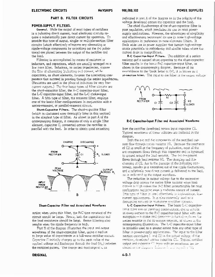
ELECTRONIC CIRCUITS NAVSHIPS
PART D. FILTER CIRCUITS
POWER-SUPPLY FILTERS. G I . While the output of most types of rectifiers
i s o pulsating direct current, mast electronic c~rcuits re- auire o substantiallv aure direct cunent ior oDerotion. To . . provide this type of output, single- or multiple-section filter circsits (which effectiveiy eliminate any alternating or ripple-voltoge components by smoothing out the di: pulso- tions) are placed between the output of the rectifier and the load.
Filtering is accomplished by means of resistors'or inductors, and capacitors, which are usualli, arranged as a low poss filter. Inductors, as series impedances, oppose .L- 'I-... "' "It".-".:"" in,,lcntinn i.?! ...- ..".. ". _..~...u..,,, \r-.-_....3 . ., . . , w h i l e
capacitors, os shunt elements, by-pass the alternating com- ponents that succeed in passing through the series impedances. (Resistors ore used in the place of induct3rs ior very low- coiiefi; ocoo:~ . ! Th; !ou: S C Z : ~ tr.pes cf !i!!er circuits ore . . ,
the shunt-copocitor iiiter, the 3-C capocitar-input filter, the L-C caaacitor-input filter, and the L-C choke-input filter. A fifth type 0.1 filter, the resonant filter, emiloys one of the basic filter configurations in conjunction with a series-resonant, or parallel-resonant circuit.
Shunt-Capasitor Filters. The shuntropocitor filter (which is discussed more thoroughly later in this section) i s the simolest tvoe of filter. As shown in part A of the . . accompanying diagram, it consists of only a single filter element, capacitor C, connected onoss the rectifier in parallel with the lwd. In order to obtoin goad smoothing
CH4RGE DISCHARGE
FROM RECTIFIER RL ILOADi
-
Shmt-Co~acitor Filter and Associated Wove~orrns
action when usiny this filter, the P.-C ti-e constant of the circuit snouid ue lorye. iiarcr, btir the icpaciiar~cs cr.2 the iwd resistonce shouid be iorge. Better iiirerinq oisu results when the ripple frequency is high.
Part OY nf the dio:rsm i!!sstrntes thy jnp,~t tnd rjnl>tnl>t
waveforms of the shunt<apacitor illlei, using a mediux to large value of copocltonce i n a fuii-wove rectiiier ciicult. C.,miitoi C initin!!,! chc:ges x :r: t% peck ucise ni !be ,)vi,lieti ~ol taqe ar,d&sck,~r~es tk,rc;:h, :kc !xi ( 5 ~ ; be?>!eec the r e n i i i d pulses. ' ihe cnargr ana alscnorqe or L 15
9W.WO.102 POWER SUPPLIES
indicated in port A oi the dioqron. as is the polarity of the voltage developed m o s s the capacitor ond the load.
The chief disadvantage of the shunt-copocitar iiiter is poor regulation, which precludes i ts use in most power- supply applicotions. However, the odvantoges of simplicity and eifectiveness recommend its use in some high.-voltage applications in preierence to more elaborate fil:ers. It finds wide use i n cower supplies that !urnis* krg",~ooitsge anode potentials to cathoderay and similar lubes where the current drain is insignificant.
R-C Capacitor-Input Filters. The oddition oi o series resistor ond o second sb.unt copacitor to the shunt-capacitor filter results in the h s l c R-C iapacitor-input filter, as shown in the accompanying dloqram. Becouse of its r~cernhionce to the ';reek letter 3i In). 11 is known os a pi-sectaon tiltat. iiie inpul iu ii,e fiiiri 1s i r . r U U L ~ U ~ vu!iui-
R-C Cqacitor-Input Filter end Associated Waveforms
irom the rectifier developed oc:oss input capacitor i l . - 1 ypicoi woveiorr!!~ oi ii~rbr ~oi i iq i .6 are inch;& :;. :kc
diaqrom. %!h !he a< 2nd d r cnrnpnnenr.s. ci tile rectified cur-
rent f l w :b~au.;h rer:es reslstsr ?,!. aecnuse the renctonce oi 22 is small ot the frequency of pulsutian, most ;: the o-c component flows through t5ls ccpccltcr ani: 1s bypzsse4 :; q:cxd ~ I O U ~ T I !'.e !x? res!s!9r. 7". 4-c rmpon?nt fiows through ioad resisror Z2. T E ~ ci>urgiiy c i r d dis- charging of c:, Jue :c the ;.;ss;$e 3f tLc ;dcc!in; cs-- panent, results in a smoothinq out 01 t'ne rlppie iluctuotions, and n reiotivelv pure 41rect cilrrent 1s delivered to ti-e load, 15 1s !ndrr,?rei oy t h e output .vovelorm.
The red~ction in output voltcge ?ue to the excessive voitoqe drop across the series filter resistor ivnen ihld -,s.-lt i q i i l b m l k s s t i e qC fi!ter irnnractlicbie for most -""l i--t innc u w w r a m ) ) i i i n n .--.... wen . 3 -od~mtp omoilnt of current. T h . " .. .- ... " "? ;!ire! 1s #,$-<;. c . ~ ~ ~ ~ , i " ~ i y I:, ; , , ,!i,-",j;t,l,e, Lu",. . . current zppl:c?tiocs. !t 1s i l so cor,rcnly ; sP :~ o i ; 2-"m,,",."" n" ,... "ry .",,,,,- -Lr"rr ....? >tTP 1T.,ll!!lPI CIIZII I I .~ .
L - C Copocitor-Input F i l tarr . The bosic i - C cawciiar- ln3811 !>iter on ~ < ~ n t ~ c o ! conixuk~~t~ofi, 0r.d 1s a,z,A.a: in every respect to the i-C coqcttor-input illter ~ l t t : one
, , e,CeptO,?- 3 Ct3Ke CC!! :!r3:<~y?rS ! ! , , ; , t< ' i !7>) >wh,iu,-c> tllr
series resistor ;a tne pi-scc;;;~ KO:-:;u:x, 3s ~ : i ; . . w i l I;? :!LC
accompanying iliustrat!on. 'The !>-C capacitor-input filter is proboblv used to o ureoter extent than any other ty?e oi !iiter in po~rl-supply ~ p p l i i ~ t i ~ i i ~ . ':LC :-C.J~ 10 the !?!te: sectlori callprlslnq :. a d ::t is :!,i ~ 2 1 ~ ~ : VC::-.;U L! ti.e wc t , i !~ r , Geve;owi ' I C ~ G G c o x c i t ~ r C!. T;~icz: :cc:;!ic: C9!>tl! 554 C??I"!!"r '-'I ,,,!>,,, ,,!>i,,,<,~ *<>"~i,,,,,,> d,C 1,)-
. . . . , , . , . . , . . . . . .. . . , . , .-,
ORIGINAL
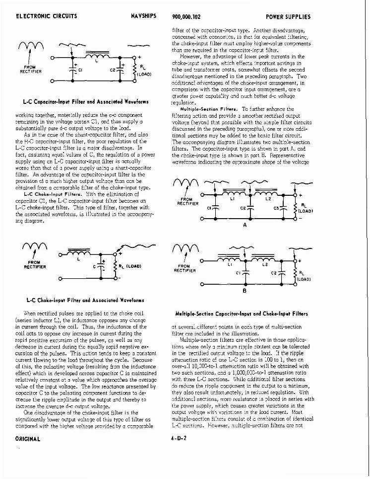
ELECTRONIC CIRCUITS NAVSHIPS
FROM RECTIFIER
L-C Cnpacitorlnput Filter and Associated Woveforms
working together, materially reduce the a c component remaining in the voltoge octoss Cl, ond thus supply a substantially pure d-c output voltage to the load.
As in the case of the shuntcapacitor filter, and also the F3-C capacitor-input filter, the poor regulation of the L-C copacitor-input filter is o major disadvantage. In fact, assuming equal values of C, the regulation of a power supply using an L C copacitor-input filter i s octually worse than that of o power supply using o shuntsapacitor filter. An advantage of the capacitor-input filter is the provision of o much higher output voltoge than can be obtoined from a comparable filter of the choke-input type.
L-C Choks-Input Fi l ters. 'With the elimination of capacitor C1, the L-C capacitor-input filter becomes an L-C choke-input filter. This type of filter, toqether with the ossccioted waveforms, is illustrotd in the occompany- ing diogrom.
m FROM
RECTIFIER
POWER SUPPLIES
filter of the capacitor-input type. Another disadvantage, concerned with economics, i s thot for equivalent filtering, the choke-input filter must employ higher-value components thon are required in the capacitor-input filter.
However, the odvontage of lower peok currents in the choke-input system, which effects important savings in tube ond tronsformer casts, somewhat offsets the second disodvontoge mentioned in the preceding parogroph. Two additional odvantoues of the choke-input orronuement, in comparison with the cawcitw input arrangerent, ore o greater power capability and much better d s voltage regulotion.
Multiple-Section F i l ters . TO further enhance the filtering action ond provide o smoother rectified output voltoge (beyond thot possible with the simple filter circuits discussed in the preceding paragraphs), one or more addi- tional sections may be added to the basic filter circuit. The accompanying diaqrom illustrates two multiple-section filters. The capacitor-input type is shown in port A, and the choke-input type is shown in part B. Representative wovefoims indicating the approximate shope of the voltage
' ' 1 ' ' FROM
RECTIFIER
L-C Choke-lnpvt Filter and Associated Waveforms
'tihen rectified pulses ore applied to the choke coil (series inductor L), the inductance opposes ony change in current through the coil. Thus, the inductance of the coil o n s to oppose any increase in current during the ropid positive excursion of the pulses, os well as ony decrease in current during the equally rapid negative ex- cursion of the pulses. This action tends to keep a constont current flowing to the load throughout the cycle. Because of this, the pulsating voltage (resulting from the inductonce effect) which i s developed ocross capacitor C is maintained relotivelv constant ot a value which opormches the averaue . . value of the input voltage. The low reactance presented by copacitot C to the pulsotinq component functions to de- n w s e the ripple omplitude in the output and thereby to inneose the overoge d-c output voltage.
One disodvontoge of the choke-input filter is the significantly lower output voltage of this type of filter a s cornpored with the higher voltoge provided by a comparable
ORIGINAL
MultipleSectien Cnpocitor-lnpvt and Chokc-Input Filters
a t several different points in each type of multi-section filter are included in the illustration.
Multipie-section filters ore effective in those applico- lions where only 3 rrinimum ripple content con be tolerated in the rectified outaut voltage to the load. If the ripple ottenuotion rotio of one L C section is 100 to 1, then on overall 10.000-10-1 ottenuation rotio will be obtained with two such sections, and o 1,000,000-10-1 ottenuotion ratio with three L-C sections. Cjhile additional filter sections do reduce the ripple component in the output to a minimum, they olsa result unfoitunotely, in reduced tequlotion. Y!ith odditional sections, Tore resistance is placed in series with the power supply. which causes greater variations in the output voltoue with variations in the lmd current. Most multiple-section filters consist of a comtinotion of identicol L-C sections. uoaever, multip!e-section !i!:ers ore not
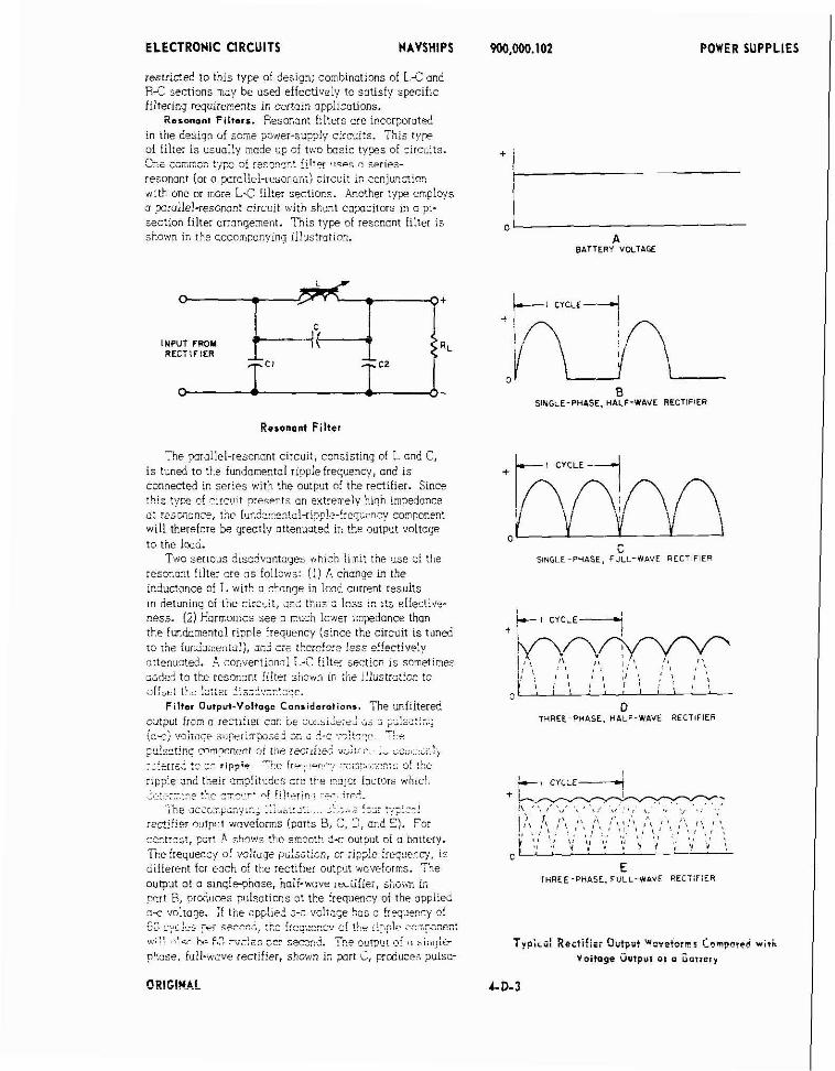
ELECTRONIC CIRCUITS NAVSHIPS
restricted to this type of design; combinations of L C and R-S sections nay be used effectively to sotisfy specific filtering requirexents in certain appllcolions.
Resonant Filters. 3eson3nt f!lters cre incarporoted in the design of some pawer-supp!,; circuits. Thk !"p~ of filter i s usuolly r . 0 3 ~ up of tv:o k s i c tyws of circuits. h-i ;;;;-o:: :;.-,- sf rez5?c~! !?!ter i ~ c e ~ o =pries- resonant (or a paraiiei-lt.sonant: ciiiui: in canj~w!ion with one or more L-C filter sections. Another type errploys a parallel-iescnant circuit with shunt copacltors in o PI-
section filter orronqement. This type of resonont filter is shown in the cccampanyinq illustintion.
Resonant Filter
The pnmliel-resonont circuit, consisting of L and C, is tuned to t1.e fundamental rinolefre~uencu, and i s . . . , . connected in series with the output of the rectifier. Since !his tiice cf Z! IC~>>~ ~ T P S P ~ ~ C I an extremely hiqh irnpedonce . ~
ut resa.5;ii:i. the ! u n ~ ~ r : ! e . ? t ~ ! - i i ~ p ~ e - i r e ~ ~ ~ ' 1 ~ ~ ~ ~ comwnent will therefore be greatly ottenusted in the output voltoge to the lm;.
Two serlaus disadvantages uib.ich limit the use of t!>e resor.cnt f~lter ore os !allows: ( 1 ) A change in the inductance of L with n ciange in lwd current results I" detuning of the circuit, m i t%; 3 loss :n :Is e!fecti,ir ness. (2) Hoi-ionics see 3 rruch 10mr ~mpedonce than the !undomental ripple frequency (since the circuit IS tuned ro rhe iurd~i i .c :~t~l ; , gii2 ;;i :kcrc!c:r !sss ei!ertive!y nttenustd. A eonvertion~l L-C filter section is sometimes odde?. to tke resoncn! iilrrr shown i n !kre il2iistmtiaa to a,[oLt . 1 -..-- 4:--2,,-"*"" ,,. . b L L E , -..,"".", ."-c.
Filter Output-Voltage Considerations. The unfiltered output from a rectiiiei 53ri i e CUX~~CICI: ia 2 >Pa::::.: , , . 3 ) , p 7 , - . T! r
;.ilsctinq mmpnnpnt o! i!?r rectii~ei VY:: ; i . , .- v~..,...L:.~~
. , >tZ..=. +" ,. -- , .: . . p p i . ~ 7%- f l e ; , , c n , - . z ,-r,mc,;~-?!:, sf t!:e rippie on? the?? omp!itl;des -re !be e.on:or ioctors whish
.*- " --,,- 3 nf r i l to,, " ? .*,-, irp?. ......, r . . L . ~~ .. ... ',' . ._ . , , ,ne dLL u..,pu..7.,. , ...- *I:>! . . .~ -'..:.,: !x: ::;ic:!
: e c i f i e ~ nutpl t wnvefans (ports 9, C, 2 , an? E). Fir cc?tr=st, pcit 4 s h w s th9 smooth 3-c output of o wrrery. The frequency of voltuge p~lsu.:icii, o: :l:;le !:e?.eccy, !s different for e ~ i h oi tb.e recaf~er output woveiorns. The output of a smgiephase, noii-wuvr ini i i i t i , j:iir;i, in port R, gicduces pulsot~ons ot the frequency of the opplied o-c volrage. If the app1,ed zi vc!:;?e h:s 3 frr;-e.cy of G?, " - - ,.,,, , - . !L< . . 7.z: , ?*.rcz2: r+,c +cq:c~~"/ C! r ir ,p\F ,-,-,r,:anEn:
. - w;:: .,:<.- t i 5:. -v;izs :c: sPCor<. !ne cur"" ,, -.i,,,!:t phose. full-wave rectifier, shown in part i, prduces pulso-
WO.000.102 POWER SUPPLIES
0 A
BATTERY YCLTAGE
B SlNtlE-PHASE, HALF-WAVE RECTIFIER
L S I N G L E P H A S E , FULL-WAVE RECTIFIER
D THREE-PHASE. HALF-WAVE RECTlFiER
L
THREE-PHASE, FULL-WAVE RECT:FiER
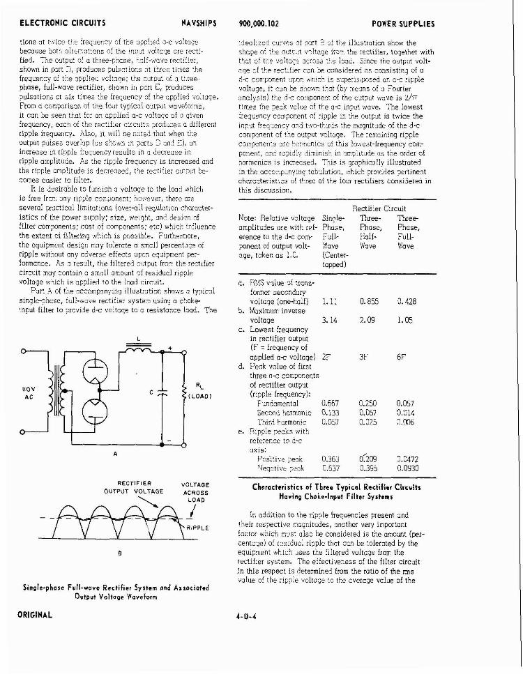
ELECTRONIC CIRCUITS NAVSHIPS
lions 31 1:iice f r e q ~ e r c y of the a?p!:e? 3-c ,voila- 3e because bolt. alteinotions of t i e !ncut :o!tzle ore recti- fied. Tb,e outpu: of o thee -pbcse , t.:lf-r:~ve rert!iier, shown in p i t Ij, produces p u l s c t i ~ n s a t tnree tires tt!e frequency of the 3pplieL vc!toce: t!.e out2ut of n t h e e - phase, full-wave rectifier, shown in part 2, pradgces pulsations 31 s ix times the frequency of the n p p l i d voltsqe. From a cn-.pmtson ai the iou: typicol a l tpu t ~viovefornls, it con be seen t t c t for an applied o-c voltore of 3 given frequency, eocn of the rectifier circui ts produces 9 different ripple frequency. Also, i t will be coted thot ,#hen the output pulses averl5p (3s siairn i n parts 2 an? Z ) , sn i n n w s e in i igpl t fre;ueniy resul ts in 3 Jecreusr ir ripple amplitude. As the r ~ p p l e frequency i s incrmsed ond the ripp!e amplitude i s decreased, t i e rectlfler oursut be- comes eosier to filter.
It i s desirable t o furnish o voltoge to the l m d which i s free iron m y ripple co;?onert; ila.vever, there s:e several practical l im~tc t l ans ( o v e r a l l r q u l a t l o n character- i s t i c s of the power supply: s ize , welght, ond desi?r. of f i l ter components; cost of components; e t c ) which i n f h e n c e t h e extent oi filtering ,wb,ich i s possible. Furthermore, t h e equipment design m y tolerate o smoll percentage of ripple without any adverse effects spon equipment per- formonce. As 3 result, the filtered output f ro r the iectlfier circuit may contain o sma!l orrount of residual ripple voltoge which i s applied t o the load circuit.
Par t A of the occompnnying illustrotion shows ; typical s inglephose, full-wove rectifier s y s t e r using o choke- input filter t o provide d-c vo!tage to a resistance load. The
RECTIFIER VOLTAGE OUTPUT VOLTAGE ACROSS
LOAD
RIPPLE
Single-phase Full-wore Rectifier System ond Associated Output Voltope Waveform
9M).OW.I02 POWER SUPPLIES
~ d w l l r e d cgrves of port 3 of tke lllustrotian show the s i c p e cl t i e outcct v l l t aqe LOT the rectifier, together with :hut cf tke vo1t:qt. 3 : r . j ~ ~ t i e ioad. Since the output volt- s q e a f t t e r ec t i f~e r can be considered 3s consisting of a d-c curpunen! door *t:lcl- 1s superinposed on a c ripple voltoge, :t con Se shown tho1 (by means of o Fourier coolysis) tile d x component of the output wave i s 2/n times the peck 'value a! 1t.e oi- input wcve. The lowest frequency component of ripple in the output i s twice t h e inpmlt frequency on3 t'h.o-tt,ir3s the magnitude of the d c component of the output voltage. The remaining ripple c m p o n e n t s a re !simonics of this lo,;,est-frequency com- por:en!, c n i iaplll,y :dimlr~sh m i r r p l ~ t u d e ns the order of harmonics i s inc~eosed . Th i s is graphically illustrated in the occu:p;cylnq tabdot icn, which provides pertinent cb.a,aracteristl;s of t h e e af tt.e iow rectifiers considered in this discussion.
Ren i i i e r Circuit Note: Relative voltoge Sinqle- Three- T h e e - amplitudes ore with ref- Phose, Phose, Phase, erence to the d-c corn Full- Hoif- Full- ponent of output volt- '?lave Wove Wove age, taken os 1.0. (Center-
topped)
a. RUS volue of trans- foimer secondary voltage (one-half) 1.11 0.855 0.428
b. Maximum inverse voltage 3. 14 2.09 1.05
c. Lowest frequency in rectifier output ( F = frequency o f applied a c voltage) 2F 3 F 6F
d. Peak value of first three o-c components of rectifier output (ripple frequency):
Fundament01 0.667 0.250 0.057 Secmd !,orrnonic 0.133 0.057 0.014 Third harmonic 0857 0.025 O.W6
e. S ipp le pecks with reierence t o d-c axis :
Positi-e p w k 0.363 or203 0.0472 ''Iegotivt -231 0.637 0.395 0.0930
Characteristics of Three Typical Rectifier Circvitr Hovinp Choke-Input Filter Systems
In addition t o the ripple frequencies present ond their respective magnitudes, onother very important factor which s u s t oiso be considered i s the amount ( w r - centoge) of residucl ripple that can he toletoted by the equipment which uses ine f~ l t e red voltuqe from the rea i f l e r system. The effectiveness of the filter circuit in this respect i s determined iron the ratio of h e rms volue of the ripple vcltoqe t c the average value of t h e
ORIGINAL
ELECTRONIC CIRCUITS NAVSHIPS
output voltage. This ratio i s expressed os prcentoge of ripple, as follows:
E. -. Percentage of ripple = 100
E," 'Where: E, = dfective (rmsj vaiue of rlppie volrooe
E,, = overage value of output voltage As 3 sine 'wcve, the eiiec~ive (rrns; vnlur ui ~ i ~ p l ~ iijkilqs con be expressed by the lollowinq equation:
2 = 0.354 (em,.-em,,, (Refer to preceding tobulct~on o! rectiiier voltage relations for percentage mlues of em,. and em,,.) An alternate way of stating the percentage of ripple, which may be found preferable in some instances, is (for a single-section filter) a s follo.~s:
where: Xc = filter capocitonce rmctancr XL = filter inductive reactance C = filter capxitsnce in miaoiarads L = filter inductance in henries
The ioctor m equals 70 for a sinqle-phase, iull-wave rectifier, 24 for a three-phase, half-wave rectifier, and 5 for o three-phose, iull-wave rectifier.
For o doublesection filter, the expression becomes:
Percentage oi ripple =--W?['ly_,, ,-.L ..~~,
in 0 fiiter system, os trleirequency oi ihe applied voltage i s innecsed (in this cose a r ipp l~ voltage), the rmctance o! o shunt copmitor decreases ond the recctonce o! c series inductonce incrmses. Tb,is neMS that the filtering ef!ediver!ess 01 any iliter rnoii? up oi shunt capociionce ond series inductance i s incrmsed a s the frequency of the applied voltoqe is increased; t h ~ s , ot the higher ripple iiequencies, iiiter cornponenrs ci smaller size u i d :igtiicr weight can je used to provide the s0.m degree ci filterin: a s can be obtained o: iower :ip;iie irquencles wit5 i!iler components a i im:>er s i re arid i.raiiri .A;).:.
Voltage Rsgulo t ion . The output voltage of a power supply decieases os tne loo0 current lncrmses oecouse oi isssez cccz:::*; !(: ,j7r1,-,,,5 ?es]s:pn::es in ::,+ :+,:t;:;c:: - d i t : ! ! !i: 3rmmpmylnq ili\lslrilt~an cornpres .i. - 1 ...- -,..-,,. 'c. ..-.... "- i i ",,.ran,c ir-." iPrfi!iur .." ,U""i'Vu,yY. .-. .-.:., .CC. ~. ~, . . ~ . ~ ~ - ~ for a simple capacitor-inpdr filter 2 ' . In; a aoke-:cpu: i , . .- 7- ---- ---- .&; -.-- +..- - 6 , , , b " , ~ ~ l ,,,. nc!rrilrr , A . , L , , .:. c"-, . - ~,. . - . ~~ ~ ~ > . . .... . ~ . .
. ., me us& in a cmtec-appe; LU.A-V..Z~VC c.x-: :c scrp ) -cr:rr !c 2 . iezticc! resictcnce Imi. il IS ~rnmeiiintely z??zrect, when c o r ~ r i n q the !,WC CUrves on the ,ytnpn, t a t while the output voitogt :or ~a:? <i;lus sf Im? ijrrent is higher for the capacitor-input crranqemer.!, the :eqdotim 01 the power supgiy is im ymrei for ihe ciiukr-i~;~ui ;i:tei.
Further s!udv of the curves reveols that in the case oi the cowcitor iriput, u ;nL:.ge ;n !oz? carrent i ; ; ~ z i ~ i ? ~ - ,L - : I ? . - - ----- .- -,Z.c, -.I:,"-"".-- .-",,:,= ;" ,, ,:<r,r, 1 I I I 1 I 1 ~ 1 I I i i T i 7 ~ l i . . ili ,...... " ,l.l.l.l ".._ ... _ _.-- -- . . . . - ..-#.--- I..... if in *" .ii ,,,;,, ,. , ,,.,: ,?,,,, ,?: , , , ,~,,,,,,<,, " ,,,<,,,, ~. .~".,. "-" ." ", -. - ...-. ...- 175 volts. For the same change in lwd current in the
-; ::i <>;ke ;;;-:, :*: d-c o-tp-. ii.!!cgt. ,F.rps !r,-,!l,
POWER SUPPLIES
0 ' , ' / I
0 50 100 1% 203 250 D-C LOAD CURRENTIMAI
Campuriion o! vollogr-iceyiiimiol? tiiaiacterisiici fa; Capacitor-Input =nd Choke-Input Filtor
400 volts to 350 volts, or a total of only 50 volts (as cornpored with the 175 volts for the capacitor inpst).
Voltage regulotlon i s a measure of the degree to which a ?ewer supply maintains its output-voltage stability under ,varying lmd conditions. The amount oi change i .
the output voltnae between the no-load and full-lmd conditions i s usuolly expressed in terms of the percentage of voltage regulation. The percentoqe of vo1:oqe rqulotion ~. is &fir& os tl-: ratic c! the $i ! fae~ce h~tuieen t h ~ ~ C T
loo,j fu:l.liiic ji:Td; vol;03is ;a :hi idll.imj voltoqe, times 100. This con be expressed as iol:ows:
(El - Ez! Percentage of voltage regulation = --- x ICC
E l
where: E: = no-lnd output voltaqe c- ' ? I I . - > ..I.... .__. - 2 = .uii-iLui uu,pur i i 2 i " j C
.2n id,! Wwer supply wou!i lo,,,e zero in!emd resist- ance (lmpedancej, ond ice percentage oI rrquiuliuii would :,e & c < G > ~ Z J ~ . S ~ I:,?IE EL Z~! !~?CEC~ ?C?,VC?> th.2 output voltage ioi the nwlwd and full-load conditions. tiowever, smce tnis is nor oiocricahie, rken rhc i ~ h r l .. ;#+:sz:G,~F ,,: ,, :,,:,;:,;:, ::,: :,::te: :!.= ::.:?r ZL: ;~;
~ n l i t b ~ nmrer the su?;rly u?picocnes on ,itjl sum;v. .., .i:".~i-"o' "" ... r -,,,,,.:,',~ ..,n,r.lliv i,,,.iW.> ii~7,:.itinn .~~ -... . . . ~ ~ - - ~ ~ ~~ ~. , z! ,. l: perc~nt 31 less.
-, -- .L.,n.!?.+l n! .i, chnlr;-inr,,t ;< ,z!hls.; , . . . . . . , x r i a ::,at 2: ::.* ~:>:<.:;!-i::~~! :::id, r L - ? .--. tho* i n r p q>nirnmiT ~ n l l i e oi Irmi current il7:rs t'rc;:l?i: t ie choke 11 i l l tlmes. kinder thls can,i?t!on, the outwt va:iaqr -hangeS in],f s:;ji,tlj ---I> -L.l-er :- ' - -A
/ / a..."ij _) L.. .""" ;men:. F.awe,,e:, :! t ie In& current 14 ~ d u c e d to apprmct n na-lmd ccnii~ii:~;, ii;r ul;ukc ;;l;llut f i i r v r l i t ;I:E ossocicted filter canoc!tor irorr cb.or%nq to tne peak voiue c: a>21ie: .vGhzp; tl-;;:, the >~ty;: .::ka;? rises !c . .. ..-- .. "...^ , * .b,- I,-,: , . , , r r u , , , ;. ,,,~ ,,m,, ! ! " ,2 ~.4 ,,," -.,,, ".,. .u.2.. .. .- :e;+ .::ice. cr :i !!:? 1~~ (1'TTE."! v.r?es b.!..i.P Zen; 1.6 ::
lo,* value, the rejulotlon will be poor as comporec Nlth tne " . " i : , , 3 , r r r r , , . . . . . . . , . _

ELECTRONIC CIRCUITS NAVSHIPS
L." ,hi. . c.. I; t t r ccse, :n ~iditional lwd ir !i.e !om a! 3
resistor, zilie? 3 bleeder resistor, is ?leer^: ;moss ti:e 32fo2t of tre filter to im?rcve the r e ;u l~ t~on 2nd establls", 3 minim~m voiue of load carrent for tne supply. This ninimm ,value of current, which flows through the filter cb,oke, improves the regulation of the power supply. The volue of the current drawn by the bleeder resistor is usuilly 10 to 15 percent of the totol current ovoiloble iron tne supp!.,. - :he bleeder resistor ocross the output tsrminais of tne power sunply not only ossists in mointoining good volto?e regulation, Sut olsa prevents the capocitors in the f;ltci system !ram charging up to the peak value 31 the cpl led voltooe. In additlan, the bleeder reduces the pcssibillty of electrical sicck to personnel, because tbe capocltors will discharge through the bleeder resistor after t5e power s ~ p p l y hos been turned off. In nony power supplies the bleeder resistor takes the forn of o valtcge div~der, either a tappe:' resist01 or 1 number of series resistors selected so thot several volues of output voltoge can be supplied to various loads hovinlj different '~0l:c;le and current re<uiier.ents.
Filter Capocitorr. A common type of capacitor used 2.i 3 fllter element in mony receiver-type power-supply circuits is the d-c electrolytic copacitor. iyithin the container of the electrolytic capacitor, rolled a1uminu-i- foil plates are immersed In an electrolyte which is corcanly on olueous solution of boric ccid ond sodium borate. The a c t ~ a l dielectric in this type of capacitor 1s
the thin oxide film which forms on one set of piotes in the lresence at 3 d-c polarizing voltage. The oiuminum foil acts a s the mode (positive terminal), and the electrolyte ccts os the cathode (neqative terminal) of the electrolytic ccpocitor.
There ore twogenerol types of electrolytic copocitors- the net type and the dry type. The piysicol chorocterlstics of tile electrolyte used determines the particular type of c3pacltor. The Net type uses an aqueous electrolyte in o metal container; the dry ty?e uses o viscous or paste electrolyte, and is ilvoilahle in either o wper (cardboard) 01 hetol contoiner.
The nost comxon working voltages for electrolytic ca?oc!tors (both types) r u n between 6 ond 600 volts. Prscticol volues of copocitance run anywhere from 1 or 2 ~ ina fo rods to os high os 2000 microicrods, the porti- culcr voiue depending on the resuirements of o given ~pplicotion.
In keeping with the necessity for a wide range of working voltcqes ond capocitonce volues, electrolytic capacitors ore nvailoble in a variety of physiml sizes. Cmerolly speokinq, the higher the voltage and the grectei the capacitance, the larger the physical slze. For low-voltage oppllcations, much greater capocitonce is lrovided in units of smaller size thcn paper-type copacitois hhich provide only obaut one ten-thausondth as much copacitonce).
!~!ult~ple-section electrolytic capacitors, which have two or -are capacitor units housed in o single contoiner, cr? extensively used ir. receiver power-supply circuits. - :or eno~~ple , 0 ai-section filter circuit may use o dual- sectlon electrolytic ccipacitoi having two 8-microfarod sections, one connected on eoc?. side of the series illter
900.000.102 POWER SUPPLIES
ele-rent. However, the copacitmce of the different sections need not be the same. In o typicol three-section cnpacitor, for instance, each section mny ha'ie 3 different copccitance, ai tiio sections may have the sa.r,e value ond !k,e thlrd section o different volue. Any number of cambino- tions are possible, and standardization is the exception rother tk.on the rule.
In addition to the electrolytic capacitor mony other nonpolarized types of capocitors ore in use: for exorple: poper-fo~l. ,*,ox-impreanated or oil-impreqnoted, oxide film, mica, and ceramic. For hiqb.-voltage applications such a s transmitter power supplies, the individual units ore larger and hove insu!ated busi.ing-type terminals. Tt.e higher the voltore, the lziler the unit for o given copoci- lance. Poper-foil types ore generally used ot voltoges frorr 750 to 25W volts. Oil-impregnated types zre used for voltages of 1500 to 3500 volts (up to 30 kv for lorge commercial installations). Vico ondceramic capocitors are genemlly used as blocking copocitars or in tuned filters, since their size is usually limit& to volues less than 0.25 microfarod. Small, hand-portable equipxents sometimes use series-connected receivinq or low-voltage- type electrolytic capacitors for economy (the price of two low-voltage units is considerably lower than one hi;h- voltage unit). Since the introduction of tionsistors, ex- tremely low-voltage (2, 4, 6, and 1 2 ~ o l t ) copacitors of very smoll physical size, with capacitance values on the order of 50, 100, and 150 microfarads or more, ore in common use to supply high currents at the lo,# voltoges employed. These capocitors ore used in power supglies which eliminate the necessity for, and expense of, battery replacement.
SHUNT-CAPACITOR FILTER.
APPLICATION. The shunt-capacitor filter, a s previously stated, is
the simplest type of !ilter. The application of this filter i s very linited; it i s sometimes used in extremely high- voltoqe, low-current power supplies for ccthode-roy and similar electron tubes which require very little load
c-went from the supply. This filter is oiso used in applico- tions where the power-supply ripple frequenq is relatively i-igh, e.g., to filter the output of a dvnamota.
CHARACTERISTICS. Cclpcitance and load-resistance volues must be high
(lorqe R-C time constant required). Load current must be rehtively small if filter i s to
have 1003 regulation. Filtering efficiency increases as ripple frequency is
increased. Regulation of rectifier-type power supply i s poor with
this type of filter: voltoge regulation depends mainly on volue oi copocitor.
CIRCUIT ANALYSIS. Gsnsrol. The rectifier circuits previously described
in this section of the handbook provide a rectified output voltage, across the load resistance, which hos a pulsating wovefarm. The occompanying ill~stration shahs o simple shunt-copccitor filter and the woveforns oStclned when the
ORIGINAL
ELECTRONIC CIRCUITS NAVSHIPS
innut to the !liter is sbtoired 11371 el t jer 3 'i3;!-r.;vc CT
0 lull-dove (s~n~:rs! ,ose) r i c t l i i t i zircuit.
INPUT '\ i ~ I
lL U i i P U T i i R O U RECTIFIER
tiRtUTi JTC ,)
- 1 1 *, 1- -
". I .., j f HALF-WAVE R i C T l
= , , r :
FULL-WAVE RECTIFIER n
HfiLF-WbYE P E C T ' F E P FULL-WAVE R E C i i i i E R
M E D L I N - W L U E FILTER ib?bC;TOh
Shunt-Capacitor Filter and Woveformi
W0.000.102 POWER SUPPLIES
the internzl reslstocce 3i t . ~ rect:i!ei, b:!t oi nwcb z:r re lc : l , i l~ !c:;; t?e:e!cre, :?e "-'I C%I,~C !L-e for t h p clrc.;lt I; rel:ti%.el: skzr:. '; c :i:u!!, *!,el the n u l i c t l r j volts:i is iirst : rs l~z: :a tne ~ t 2 l t < 3 F a ~ : t 3 1 f i l t e ~ , the c ~ i o i l t c r c'.;r.;es rcyl4l.i : lxst rnehes tile peak v n l t ~ l e ~ l ~ ! b ' , f i t?e first ieh eyilei. T ' e ch;:.;e cr ti.?
, . . c>>~c l to r i;;rCxlm;!es :-e ;i;i L.:IJ~ 31 :re ;czti!:e: . . - 3 ,u. , -_F .... ,ire-'"- , ---.. '.". '" - --.,. -..-- ""d .-.A" ,'.. j..c ,, .il.l. ii .... " -.....,, ""
iet;:n 1:s ckorje ;:re" !he rrcti!:er output h!!i !O Z ~ I L
::::xe t ) . ~ z:scit?r r2rnni il;c.:jrl; : - - p l l ~ t ~ i V j . -,,:
m2ocitor slowb, 31schorjes !:lroiqh the 1 0 ~ 3 r e s l s t x - 5 . ';, c x:?? t t ? ! i r e !re rec!~!irr i i c n r - n n + u c t ~ n ~ . ~. . . TL,r rote ii : l i - i r l e :a: ::e c::::::s: :: ze!e~::.ln:: 5,; 1 - 0 !?n res::rlrce- ,! 1.r C::,??II~>~ ir.5 ]3c.:-leslsl~ t
. . . . .?. :;. ,. . ride: ;!c L , , . ? , : ( I < . ' - , ...,. ,., ,% ,, , .,, ,.L L.,kdt - . . ~~ . . -. .. . 1. LC' E L / lb.,,. ,.C . . , .... I.. _ -. . ..
T * . , :::lr!!?:~?-:. !! < ! 7 .,- seer .-7, ::e <.7,t,:,:, O ! c,,:dcltLr . . , , . .. - .. , , , < , - ~ , , ,. , , , ,. ,: ,,.<?, .* r 1.c: ;.;?:: ;:, .;,;it.? ~. .. . . .~ . .--A .. . . . ': -8::':t ,0::2,><-, : ,:", - -~: 2 re7,::t:"C :,, :.,, :;:L,l<-
.. .."f~,e:#:, u c , ..>L.,C?.t :,2r:.: :'~.= i?G: c::::t:?,c2.
.-~s prevlotls~y s tc tec , trle capozlrar S r u o ~ i y 01s- tLrs.;- tLs :LO:. il-r-l:: :ie 3-tT.?i \,cltc:e
, ' . - ---.--. . . ."e-: 'e --:',t ,.*c li . , , , I_> ... " C _ L a c Y L L I 1 3 , .... l i " i l "" : , J + >.->a :> ,L,> .,-,, " ' . . - ! , - " c , -7 -nq,.c, 1 ., .. . .. . .... . . . . > ,. 'Y,
!be ccpczitoi once nqnin sV;rts c h u r l ~ n q to the peok value. . . 8 . ?:o .,-:.,- m; ;A. - . ~ ~ ~ : t n : . , s ~ d tbP f i l ter rlrr,,;t . . . . . . . . . . . . . . . .
ELECTRONIC ClRCUlTS NAYSHIPS
output voltoqe. For this reason, the shuntcawcitor filter i s seldom used with rectifier circuits that must supply o relctively large lmd current.
The pulsations ocross copacitor C and imd resistance R L , no matter how small in amplitude, ore in effect a fmm ot distortion. hlthough these pulsations represent a fundamental irequency, many other frequency components ore also present in the output. In the majority of equipment opplicotions, the presence of a ripple-voltage component i s not desirable: therefore, fa most equipment application it i s imptocticoble to use a simple shuntsopacitor filter; additional filtering (or another typ? of filter) i s necessary to reduce the ripple amplitude to on acceptable minimum.
D.toi1.d Circuit Operotion. Consider now o complete cycle of oprotion, using a single-phase, half-wave rectifier owrotina with shunt caoacitor C and imd resistonce RL, shown in the preceding illustration. Copocitor C i s assumed to be large enough to insure small reactance to the pulsating rectified current. The resistance of RL LS ossumed to be much oreater than the reactonce of C a t the input frequency.
When the circuit i s energized, the rectifier conducts on the positive half of the cycle, and current flows into and choiges capacitor C to approximately the peok volue of the input voltoge. The chorge is less than the peak value of voltoge by the amount of the voltoge drop ocross the rectifier tube. The chorge 02 C i s indicated by the heavy lines on the waveforms in parts B and C of the illustration.
On the negative hallcycle the rectifier cannot conduct. since the late is neaative with resDect lo Lhe cathode. !luring this interval, capacitor C discharges throuoh lmd resistance RL. The d i s c h r ~ e of C produces the downward slope of theheovy lines in borts and C of the illuslration. In contrast to the abrupt fall of the applied a s voltoge fror peck value to zero (shourn in dotted lines), the voltage across C (and thus ocross Rr l during the dischorge period decreases ot o graduol rate until the time of the next holfcycle of rectifier operation. For o given value ot lmd current, the value of C determines therote at which the discharge voltoge decreases. This rote of voltoge decline and the value of Care inversely related. Thus the rote i s greoter for smoller values of C and less fa greater vai~ues af C. This indicates that fa the some lmd current, if C (or RL) is increased, the ripple component in the output to the lmd i s decreased. (A longer t ine constant requires a longer time to charge and dischorge.)
Since procticol values sf C and RL insure a more or less grodual decrease of the discharge voltage, a sub stontiol charge remains on the capacita at the time of the next half-cycle of operation. As a result, no current con flow from the rectifier until the rising a s input voltage on the rectifier plate exceeds the voltoge of the charge retraining on C, because this chorge voltoge i s the cathode-toground potentiol of the rectifier tube. &'hen the plate voltoqe exczeds the charge voltage across C, the rectifier again conducts, and again charges C to a?proximote!y the peak value of the applied voltaqe. Shortly after the charge on the capacita reaches its peak
POWER SUPPLIES
volue, the tube stops conducting. Because the fall of the a s input voltoqe on the plate is considerably more rapid than t.he deneose in the copacitm voltoge, the cothcde quickly becomes more positive than the plate, ond the rectifier ceases to conduct. During the charging period, capacitor C is connected ocross the output of the rectifier, ond the chorge time isdetermined by the efiective series resistance, which is only that of the tube plate-to-cothode (fcrward) resistance and the trons- former impedance, plus that of the leads to the tube and capacitor. Hence, the resistance is low and C charges very quickly. During the nonconducting period, the dis- charge path i s through RL, which i s relatively luge, so that the time constont i s long. Thus copacitor C does not discharge appreciably before the conduction cycle again bwins.
The repeated chorge and dischorge of capacitor C (as described above) with the respective rise and fall of the input voltage constitutes the basic filtering action of this circuit. To reduce the ripple amplitude and increase the d s component in the output voltage, copacitor C charges up and stores energy when the tube is conductin and discharges to furnish current to the lmd when the tube i s nonconducting.
E Using olms low, R = -, it is evident hot a h m y
I
current droin, for the same output voltage, represents a lower lmd resistance. Therefore, with a heavy lmd and lower RL, copacitor C discharges more quickly. Since the output voltage represents the overage charge retained in the capacitor, it can be seen that with heavy lmds the capacitor will discharge further between the perlcds of tube conduction. Hence, the output voltage will olso be lower. This i s why the singlecopocitor filter is used only for very light current drains. Since the output voltage for heavy l a d s i s lower and the output ripple voltage component is also higher, the effective filtering is gwd only for light lmds.
FAILURE ANALYSIS. General. 'Xith the supply voltoge removed from the
input to the filter circuit, one terminal of the filter capacitor can be disconnected from the circuit. The capacitor should be checked, using a capacitance analyzer, to determine its effective caoacitance ond leakaoe resis- tance. During these checks it is very important that correct wlaritv be observed. A denease in effective capacitance or losses within the capacitor cnn cause the outou to be below normal and also cause excessive ripple amplitude.
If a suitable capacitance anolyzer is not available, on indication of leakage resistance can be obtained by using on ohmmeter. Resistance measurements can be made ocross the terminals of the capacita to determine whether it i s shorted, leaky, or open. When testing electrolytic capacitors, set the ohmmeter to the high range and connect the test prods across the capacitor, beina careful to observe oolaritv. This is imwrtont becouse current f!ows with less opposition thrmgh an electrolytic copacitor in one direction tban in the other.
ORIGINAL
ELECTRONIC CIRCUITS NAVSHIPS
If the correct polarity is not observed, an incorrect reading will result. !';hen the test prods ore first connected, a large deflection of the meter tokes place, and then the pointer returns slowly toword the infiniteohms position os the c o ~ c i t o r charges. For o g o d copacitor with a roted working voltage of 450 volts, dc, the fino1 ieadinq nn t h p ohmmeter should be over 5W.OW ohms. (A rough rulc cf thu-b !or hiqh-voltage copoc!!nrs is at least 10% ohms per volt.) Low-voltoge electrolytic copacito;; (below 1W volts roting) should indicate on the order of 100.000 ohms.
If no deflection is obtained in the ohmmeter when rnokln~ the resistance check explained above, an open- circuited ccpacitor is indicated.
, -.-- J.. '..>> ---,- An',""*;n" "4 ,ha n"<",m, ", .,,-"7 ,".. -.".-" -..*-.. -. r... ~~.~ -~ ~ ~
ohms indicates thot the capacitor being tested is short- c~rcu~ted.
An indication oi a leaky copacitor i s o steudy read- iclg ,:,,? rLe i-;!e sc~ewhe;; k!wcm zero c d the mini- mum acceptahle value. (Be certain this readinq is not caused by an in-circuit shunting part.) To be valid, these copocitor checks should be made with the copaci- tor completely disconnected from the circuit in which it operates.
In high-voltcge filter capacitor applimtions, paper ond oil-filled capacitors ore used, a s also are mim and ceramic capacitors (for low-capacitance values). in this case, polority is of no importance unless the capacitor terminals are rnorked + or -. It is , however, qccd maintenance practice to use the output polarity of the circuit as a guide, connecting posltlve to positive ond negative to negative. Thus any effects of poiority on circuit tests uie rr,ini,aize? snd the jossihility of damage to conponents or test eqwpment is avoided. Rem-mber-
on undischorqed copacitor retains its polarity and holds its charge for long periods 01 time. To be safe, discharge ri:r copxitor to k tested nith the p o l a r O F F kfore connecting test equipment or disconnecting rhe mpacitor.
A slmple check which can be used to quickly determine whether the copncitor is at fault is to substitute a known 2cxd capacitor a! the some value ond voltoge rating and note whethe: !be circui! operotlo" leturns 10 noriol.
R-C CAPACITOR-INPUT FILTER.
A?PL!CATION. Tte ?-C ca;ocito~ir.;-: filter is !:n!!d to 3ppil-
cc!ior.s ;n which the lmd cyrrent is sncll. This type oi filter is used in johe; sapplies where the imc cilirent is constant and voltoqe regulation is not necessary, such :: ir !+c \i;h.-v?!tci.e ~i lppi" for 0 cotnme-roy tube i r as pc:! of c de-couplinq network for multistage ampiiiiers.
CHARACTERISTICS. Fi!!.! is cnmmseil nf qhtlnt input capacita, series
res js ta , and shun1 output capacitor. i!itertnc eff~ciency increases os rippie frequency is
:.,b.xsec. " ...-.. . -....-"I i " -,.rh iorc t M n ,nnr ""mind from uu,w" ,--,..., .- .--" . . . . .
Laresponoing iiitei nnii;. rsrh ; ;ilur.s i.i,c-..
;es:stor.
900,W0.102 POWER SUPPLIES
Regulation of rectifier-type power supply i s pwr wlth this type of filter; requires relatively constant imd current.
Rectifier wok current i s high with this circuit be- cause of input capacitance.
CIRCUIT ANALYSIS. The rectifier circuits previously described in this
section of the handbook provide o rectified output voltage (across the lmd resistonce) which haso pulsating waveform. The accompanying illustration shows an R-C copacitor-input filter and the waveforms obtained from eithn o half-wave or a full-wove (single- phase) rectifier circuit.
Erl
i L I r HALF-WAVE RECTIFIER FULL-WAVE RECTIFIER I 0
VOLTAGE ACROSS CIPACITOR Cl
R-C Capacitor-lnprt Filter and Worrfamr
- .ne woveiorir:~ shornl in ;orl .A. iepiesent t ie ~~.;.lllir;
ed output from a typiml rectliier circuil when currenr ydses flow though !he i d rrsisiance each t i m the :e;:i!ie: cscducts. Xote !hot the dashed !ine id icot- inq the overaqe value of output voltaqe, Em,, for (he 1a.1-h~ve rec t~ i~e r is !ess :n3r. XI! tne a-?I~llde .i :.-e vol!z.c 9 e c d s ':?pox 0.3:). P . e o,er:?e v::~e of . ~
~ ~
olitpu: voltage, E.,, for the full-wave rectifier is q r w t n .i_ .,,,n ha!! !apwox 0.65). but is s!ill milch less tnan the
-ii ur~~oiitude 0; th i rec:iiieiaiiti;li: ,;;~1.ef3[i. ?.:i:h ?.o , . ,'.... :. . .. --" -,,-... 2 --.-p2 .L- -,,,-,., -. ,-m .*r;::;s. ...~.. .-.,
c!:c-it !~n!i!terd!, the iliirue!mm hn_s n Iorqe vnlue of
ORIGINAL
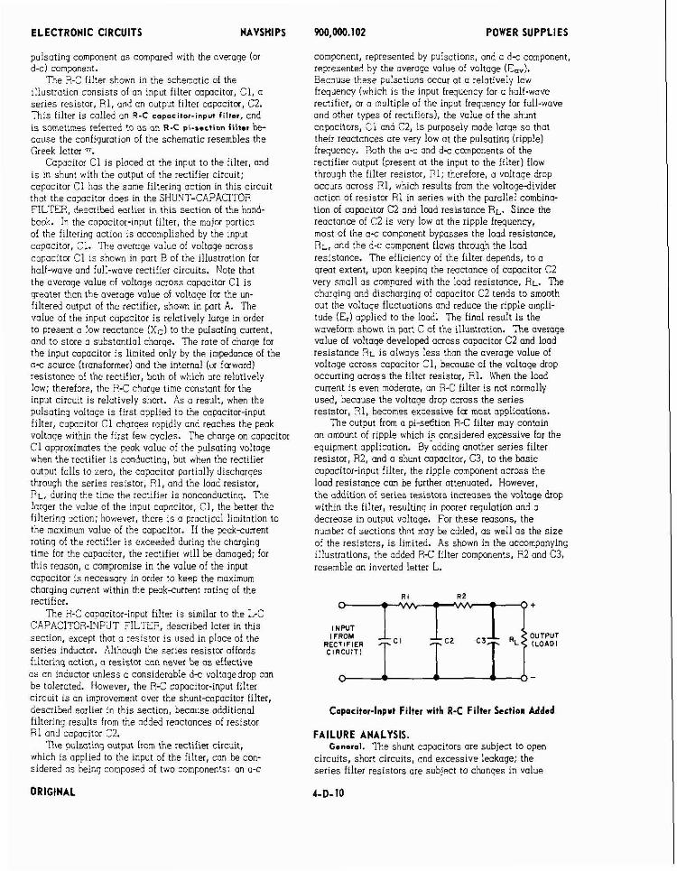
ELECTRONIC CIRCUITS NAVSHIPS
puisoting component os compared with the average (or d-c) component.
The P,-C filter shown in the schematic of the lllustrotian consists of on input filter cowcitor. C l , o series resistor, R1, and on output filter capacitor, C2. This filter is colled an Q-C capacitor-input filter, and i s sornetnnea referred to os on R-C pi-saction lil+er be- cause the configuration of the schemotic resembles the Greek letter n.
Capacitor C1 i s placed ot the input to the filter, and i s in shunt with the output of the rectifier circuit; copocitor Cl has the some filtering action in this circuit thot the copocitor does in the SHUNT-CAPACITOR FILTER, described earlier in this section of the hand- book. In the capacitor-~nput filter, the major portion of the filtering action is occomplished by the Input copocitor, C1. The averoge volue of voltaqe ocross capacitor Cl 1s shown in part B of the illustration for half-wove and full-wave rectifier circuits. Note that the averoge value of voltoge across capacitor CI i s gieoter than the overoge volue of voltage lor the un- filtered output of the rectifier, shown in wi t A. The volue of the input copacitor i s relatively lorge in order to present a low reactance (Xc) to the pulsoting current, and to store a substantiol charge. The rote of chorge for the input copacitor i s limited only by the impedance of the a s source (transformer) and the internal (or faword) resistonce of the rectifier, both of which ore relatively low; therefore, the R-C chorge time constant for the input circuit is relatively short. As a result, when the pulsating voltoge is first opplied to the copacitor-input filter, copacitor C1 charges rapidly and reaches the peak voltoge within the first few cycles. The charge on capacitor C l approximates the peak volue of the pulsoting voltage when the rectifier i s conducting, but when the rectifier output falls to zero, the copacitor partially discharges through the series resistor, 81, and the load resistor, RL, during the time the rectifier i s nonconducting. The larger the volue of the input copocitor. C1, the better the filtering xtion; however, there i s a practical Iimitotion to the maximum volue of the capacitor. If the peak-current rating of the rectifier is exceeded during the charging time for the copacitor, the rectifier will be damaged; for this reason, a compromise in the value of the input capacitor is necessary in order to keep the maximum charging current within the peakiurrent roting of the rectifier.
The 3-C capacitor-input filter is similar to the L-C CAPACITOR-INPUT FILTEP,, described later in this section, except that o resistor i s used in d a c e of the
as an inductor unless a considerable d s voltagedrop can be tolerated. However, the R-C capacitor-input filter circuit is an improvement over the shuntsapacitor filter, described earlier in this section, because additional filtering results from the odded reactances of resistor 91 and capacitor C2.
?he pulsatinq output from the rectifis circuit, which i s applied to the input of the filter, can be con- sidered as being composed of two components: an o-c
ORIGINAL
900,M)0.102 POWER SUPPLIES
component, represented by pulsations, and a d s component, represented by the overage value of voltage (E,,). Because these pulsations occur at a relatively low frequency (which is the input frequency for a holf-wave rectifier, or a multiple of the input frequency for full-wove ond other types of rectifiers), the volue of the shunt camcitors. CI and C2, i s ourwselv made larae so thot . . . . their reactances ore very low ot the pulsating (ripple) frequency. 80th the o-c and d s components of the . ~
rectifier autput (present ot the input to the filter) flow through the filter resistor, R1: therefore, a voltoge &op occurs ocross Rl, which results from the voltaaedivider action of resistor81 in series with the paralleicambina- tion of mrncitor C2 and lmd resistonce RI . Since the reactonkof C2 is very low at the ripple frequency, most of the a-c component bypasses the load resistance, RL, and the d-c component flows through the load resistance. The efficiency of the filter depends, t o o great extent, upon keeping the reactance of capocitor C2 very small os compared with the load resistance, RL. The charqing and dischorqing of capacitor C2 tends to smooth out the voltoge fluctuations and reduce the ripp:e ompli- tude (E,) opplied to the load; The fino1 result i s the waveform shown in part C oi the illustration. The average volue of voltage developed ocross capacitor C2 and load resistance PL i s alwoys less than the overage volue of voltage across capacitor Cl, becouse of the voltage drop occurring ocross the filter resistor, Rl. When the lood current i s even moderote, on R-C filter is not normolly used, becouse the voltoge drop ocross the series reshtor. 71, becomes excessive fa most oppiications.
The output from a pi-seftion R C filter may contain on amount of ripple which is considered excessive for the equipment application. By odding another series filter resistor, R2, and o shunt capacitor, C3, to the basic capacitor-input filter, the ripple component across the lood resistance can be further attenuated. However, the addition oi series resistors increases the voltage h o p within the filter, resulting in poorer regulation and a decrease in output voltage. For these reasons, the number of sections thnt may be added, as well a s the size of the resistors, i s limited. As shown in the accompanying illustrations, the added RC filter components, R2 and C3, resemble an inverted letter L.
Capacitor-Input Filter with R-C Filter Section Added
FAILURE ANALYSIS. G.narol. The shunt capacitors are subject to open
circuits, short circuits, and excessive leakage; the series filter resistors ore subject to chonges in value
ELECTRONIC CIRCUITS NAVSHIPS
cr., occcsionall:, to Open circuits. A7.y of these troubles con be eosily detected.
Tk,e mput irjwcitor has the ;reotest pulsot~rg ,volt- 7-e cp;!i.-? !a i!, is t i e ~ . c s t sm~sceptibie to voltoge suiqes, cnd iss s b,i:her weroge ~ l t o g e appli*?: 05 o i ~ t l l f , fhe !npu! ccgacitor is frequentiy subject to voltage breuk- "own in4 ~hnrfio:. T ~ F i-mcinlni sili>nt cc~oacltorisi in .L- a<,.... - t .... ..-, .,, =,,, -p" , , co L t 2 C & . A L C , L L . L U . L A- ,,=. .- "u.."y. -".y."
c ! h e ~.?teteinn offered by !be ;?rips filter r?siitorfs): no,aever, o s%nt copocitor ccn oecome open, Inky, or shorte?.
Sborte6 cooaclt01s 01 cr. ocin iilter resistor wiii ieslii! i n ,I nc~oillput ~n-i;cui;on. h? cpcn f;:ter reslslor :::li result 1.. cn ~bnairrali~! ::!a!! - c voI!,>t~~ .>! tije mpjt . . . . 1 . . . . .-.......- '.I.... ............................. , . . . ,",1", ......L. ...-. . L e , ~ k . ~ capncitors or filter resistors that i.cve increased ir v318:e &,i l l i r s l i t ~n o iow 1-c output voir::$r. 2pm r lpc-lrors, rnpncltors .unlc:l r l l lvr 1051 tr.elr r f i e c t l ~ m e ~ s ,
, , . - . . . . I ! ..... 1. ' ! : i ! ! 2 , . ! ? , , , - , , . , ic ~ ~ D Y c D E C ~ ~ ! F . !in?!? ?m?!!t!ld~( in th r otllnilt nf tile . . supply.
&irk me s u o p l ~ voltaqe removed from the irwut to the . . . filter circuit, one terminal of mch copacitor can he disconnected irom the circuit. Soch capacitor shod3 tr checked, using a ciipocitanie z n a l ~ e : , la 5ete;m:ne ?!r effective copacitonce o~.d !maage resistncce. It is importnt that correct polority be observed ot 011 times. P decreose in effective capocitonce or iosses w~thi- the copacitor con couse the output to be below nnrmnl ond olso coure excessive ripole ornolitode. Tne
~ ~
c f :esislorr be b!{ , ~ ~ i ~ . ~ ZF ~ i - r e t ? : .
!f z suitoble capacitance c~ialyzer i s not ovcilable, ;r ;r:c;tlor. ci ie+,zge reslstcncr ccr~ k~ a i i ~ l r ; c i L: using en ohmmeter. Hesislence immsurerricnts sun be mark across the terminals of the ccwcitor to determine 'whether it is shorted, open, or ieaky. *hen testinq
. , , , . , eiectro~yt~c cagac~tors, se: tr,e oxz.mc:er rz I!W .?lg.n range ond connect the test prods oROsS the capacitor, being careful to observe polarity. This is important i I1 -.... ... ;,k laic nnnnci(,nn thmllnh nn
L" ..b,.. .<u. .4 ...... -ry-u ....... ... :lectrolytlc cu?jcitor in ofir direction t i i i in :he st';=. .... 11 ~e ~ c ~ ~ ~ r e c ~ p o ~ ~ i i ! ~ ia raGl abse?;d, iccc;rect
. i . - ..i" . - - m i , ':,h." '"+ !e%! Cl"i qTF :!rcr .. ................... connected, 3 loige dellection of thc meter tnkes place,
. . a,; ,;;e;, L..C >", , ,<C, , ~ i " , , , > > : d * : y :G.?"T: ::-,e ;7:::,.:: -~
, . , -... .. ...... - - - - -- -- .L^ _:,._"n;. .:..,.. 1 . . .................... . , . L"cGzicar *;,,., ,> r - . . . . . . . , .-" , , "l*" *".h..i, .".,;<C 2; 'i"" .L..*, "-, . . . , , . , . . . - . . . . . . . -> ....................... s,:v, ,',~,,. ? I . . , , - , , ,, , , , - . , , Fir, _l,,iiii.u .,,. ~..C: .,,. "."-L zn-5. i.4. rcu;? ruic n i rn,yi!r i i i r n:!r-vnhru it. I 1 1 ! I I o ~ l c l i 8 ~
'-?;! 1""" -L-- ..^I. , I ^.. .-.."I._^" nlart.nl. . . .r . ,. , , . . . . . . . . . . . . . . . . . . . . . . ." .... "- . . .?A / . . : i . l i 1 ......... . . . --r" -..- ;a .- L...~ .J. . ...... ,. - . . . . " m n
or??: nr 13u.wG a i x r . i! no detlectlon is olitninen on lne an-!.ere: wnen
,,,;:<i::; ti.* :esis:;:c; c'-c=; c:<;!;;!:$? :>c....~. =* y..- c;rci!eo copacitoi is in:iciten.
5 . > ' > I -..I. >.<I .',L--":-.".-, -".- r-, "LC-iY IY I , - , I I .E iC_iC,-i'il. ": il . i I.VI..LL, ......... ohns inacotes tilot me copnc~toi oemg tests! I S snort- -. .- ... ">
L".
, , t : i , . . ;! .2 :-,A" ,-,,;.;;;:;,, i; ;, .-:s,;:.; ::;:~ ................. , . , ,
!y cp !b:e 5c2ie SC,.>?,>,V,P :F#.",w,: ,?\,. ,,,,,! i: ,= <,i .,,c,., accept-Die iolue. i3e cerlalr. tnls rma l r j 1s no: cnuseo
ORIGINAL
900,000.102 POWER SUPPLIES
Sy 3n in-circillt silu:>ting port.) To bevalid, these cc~ocitor checks silould be mode with the capacitor ;o>.>plete!y d!sconnected iron the circuit in which It operates.
In bilk-voltaye filter cowcitor opplizotions, paper mi fii:-filI& sapocitars are us&, os also ore mica ond c r r x n c cizailtcrs (for ich-capacltonce volues). , n 1.m- ---- -ninr,tv is "I no mprtnnrP ,unless the ....... - . , ......... ccsacltoi teiminols are marked + or -. It is, however, qoai nuinten.;l>ct. prnctice to use the odtput 2olarity of the circult a s a guide, connectino positive to positive ;!:i negutivr t, neyltive. Thlis any effects of polarity 39, circuit tksts l i t nl!nlrlzi-: ; n l :'he possibility of . ~. :A 27; to i z i i p n m t s or test eqaipment is avoided.
"----L.. - r - r2.--k7, --.- .-,--*7<!*F ............ ro , - i "~ i t < ?i?.~t>,
2nd !~olds its charge lor long penods ot time. l o be suie: 2;sc?,owe (he co;~cci~ur tu be tebtd #&k2 the pow-# O F F ir.Lrt ;zi;tiiiiii :is: .:iai;mtot or ?:SCOT.- ........... .--- ",,". , , ........ ; s~mgle checn wiicn con oe used to ~uicklj . derer-
mine .rhethe; a capacitor is at foult is to substitute 3 l(ntiiv11 j o d cowcitor of the sane value and voltage rotlcg ncd note 'vnetker t h ~ ci~cuil operotion returns to nornilol.
L-C CAPACITOR-INPUT FILTER.
APPLICATION. The 1.-13 copacitor-lnput filter i s one 01 the most
comrnonl~ used filters. ?his type of filter i s used ::i-crl!:. 17 :cdio rece:vsr 3 ~ 6 sndi ~?id!o mpi i i~e r power supplies, ,and ig my type of Dower supply where .. ~ . . . ~ : ,~ ,.,,-,.: ,.,,,x* -; !,;* ::< tL,? !cc< zz:e:! iz :?!:!:.:2!.! iiinSIGii1.
CHARACTERISTICS. - , . ! !:Le: :> ,-,J 7>$:,:e; ,:,I 5:,,?:<; ;7??,,: ,-,7:*7,<:c:: s2:iEs
~r.ductor, and shunt output camcitor. tiitermq eit~ciency Inneases a s rippie irequency
is !"crsased. 0:jt-,;:: va!!cy : c i ra te : !"on that of choke-input .. 4 . i .-.. "...^.,. -.,.. ^", I^rr .inn th", "6 rhnl..-inn,,, ... "'cSr, rurYui ir..i.i. ...-I ...". r r
.,l,.2r
Regulation cf iectifier-type power supply i s only .... I ... .L: -' t.8 ,-.. .-" .:.-- .al~+:,,O1,. -". . .... i.lu. ,,,.- ". ,...-., .-il..__ .-.,
, , . . . . . . . . . . . . . . . . . . -, ... - , r,L...:Lc; psi <-<z~.. ;a *:2. ::.s zi::-;: k . . ...................... ~;
L ~,~~ ......... ". C!RCUIT ANALYSIS. ; , 7%- --" ."..,-*. .. " chnu, "" , -I'
,. > ~ . - - ,,.:.: '., .. ....,.,.... I::.YL llltei iil5 the .u;~eforrns obtcine? ircm eiri.er a r:oi!-uiuve or a iu i j -wave ~ s i i t u ; ~ ~ i l u ~ r ; reiiiiiec . .
i . . . . . i t ........ - . : e ..,:~ip!c:i:!:s -i;~nr. ;rl w ? t . represent the i;nfi!ter - 2 '.".. - . ...-;""I ,oc.<l;o. *,,,-,,!, ......--..... ?,\?,en, . . . . ..?., .,r.., ". ; ; : ~ i s r s tiow through the 1-i resistunit mch tine the ; i ? . ! ! . - r .:.?ri;izrs "!,-,!= !Pot f%e .?v?.i.my wiue DI
. . .- . ...I,.- ,,..,,-"."A b, . .." 2"c,,',z :,"a,, .... ....... .....,... .u.. ""b. -,." ....-.- ".." -. -" ie: . , , ,, .. 1 .... L . . L . , ' . L ---- ,;*,,A,. I . , " . ~ t ~ . . . . . .= ,cL,i,,c. ,- ~ c a a ,.,,A, ,.-.. ,..- "..," ...- ". 3 I me ,,ouoqr pcuns, L I ~ Z uvrru.je v u ~ oi ourpbi iair-
.. ,-. .I.. , ..-.... ". -,.,. .hnr ...... ..", ?", .-. ,.,. .".. ,L -....LI .I .(.--.-. ...-..
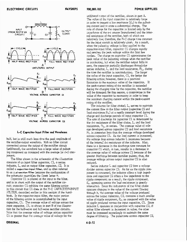
ELECTRONIC CIRCUITS NAVSHIPS 900,000.102 POWER SUPPLIES
L
INPUT (FROM RECTIFIER
CIRCUIT1 @$=--g:L OUTPUT ILOADI
A ' UNFILTERED WTPUl
I I f HALF-WAVE RECTIFIER f FULL-WAVE RECTIFIER
B VOLTAGE ACROSS CbMCITOR CI
I I f HALF-WAVE RECTIFIER f FULL-WAVE RECTIFIER
c - VOLTAGE ACROSS CAPACLTOR CZ
L-C Cqaritor-Input Filter and War*fornr
half, but is still much less thm the peak amplitude of the rectifier-output woveform. With no filter circuit connected ocross the output of the rectifier circuit (unfiltered), the waveform has a large value of pulsat- ing component os compared with the average (or d s ) com- ponent.
The filter shown in the schematic of the illustration consists of an input filter copacitor. C1, a series inductor, L, and on output filter capacitor, C2. It i s called o copcsitor-input filter, ond i s often referred to as a pi.saction f1It.r because the configuration of the schematic resembles the Cseek letter n.
Capacitor C l i s placed at the input to the filter, and is in shunt with the outout of the rectifier cir- cuit; capacitor C1 exhibifs the some filtering action in this circuit that C! does in the R-C CAPACITOR-INPUT FILTER, described earlier in this section of the hand- book. In the capacitor-input tiller, the major partion of the filtering action is acmmplished by the input capacitor. C1. The averoge value of voltage across the input capacitor, C1, i s shown in part B of the illustro- lion for the half-wave and full-wave rectifier circuits. Note that the overage vaiue of voltage ocross capacitor C! i s greater tho- t i2 a,;,;r~g, wlue of voltage for the
ORIGINAL
unfiltered output of the rectifier, shown in part A. The value of the input capacitor IS relatively large in order to present a low reactonce (X,) to the pulsot- inq current ond to store o substantial charge. The rote of charge for the capacitor i s limited only by the impedance of the 0% source (transformer) and the inter- nal resistance of the rectifier, both of which ore relatively low; therefore, the R-C charge time constant for the input circuit i s relatively short. As o result, when the oulsatino voltaae is first applied to the
cycles. The charge on capacitor C1 opproximates the peak value of the pulsating voltage when the rectifier i s conducting, but when the rectifier output falls to zero, the capacitor partially discharges through the series inductor, L, and the load resistance, Rr, during the time the rectifier i s nonconducting. ?he larger the value of the input copacitor. C1, the better the filtering action; however, there is a practiml limitation to the maximum value of the capacitor. If the peakeurrent rating of the rectifier is exceeded during the charging time for the copacitor, the rectifier will be damoged; for this reoson, a compromise in the value of the copacitor'is necessary in order to keep the moximum charging current within the peakeurrent ratina of the rectifier.
he inductor (or fiiter choke). L, serves to maintain the current flow to the filter output (capacita C2 and load resistance Rr) ot o nearly constant level during the charae md discharqe periods of input capacitor C1. The ;ate of dischargefor copacit& C1 is determined by the d x resistance of the filter choke, L, and the lood resistonce, RL, in series. The averoge value of volt- age developed across copacitor C2 ond load resistance RL i s somewhot less than the overage voltage developed across capacitor Cl. As the !oad current i s increased, the voltage drop across inductor L increases because of the internal d< resistance of the inductor. Also, there is a decrease in the discharge time constant for copacitor C l which, in turn, results in a decrease in the overaae volue of voltaae across C1 because of the greater discharge between rectifier pulses; thus, the overage voltage ocross output capacitor C2 i s also reduced.
Series inductor L ond capacitor C2 form a voltage divider across copocitor Cl. As far as the ripple com- ponent i s concerned, the inductor offers a high imped- ance and capacitor C2 offers a low impedance to the r i ~ o l e comyanent: a s o result, the ripple component, . . ~ ~
E,, appearing amass the lood resistance i s &eatly attenuated. Since the inductance of the filter choke opposes changes in the value of the current flowing through it, the averoge volue of the voltoge produced ocross the output capacitor, C2, contains a much smaller volue of ripple component, Er, as compared with the value of ripple produced ocross the input copacitor, C1. Since inductor L operates in conjunction with capacitor C2, if either filter element i s deneased in value, the other must be inoeased accordingly to maintain the same degree of filtering. The pulsat~ons across capacitor C2,
4-0-12
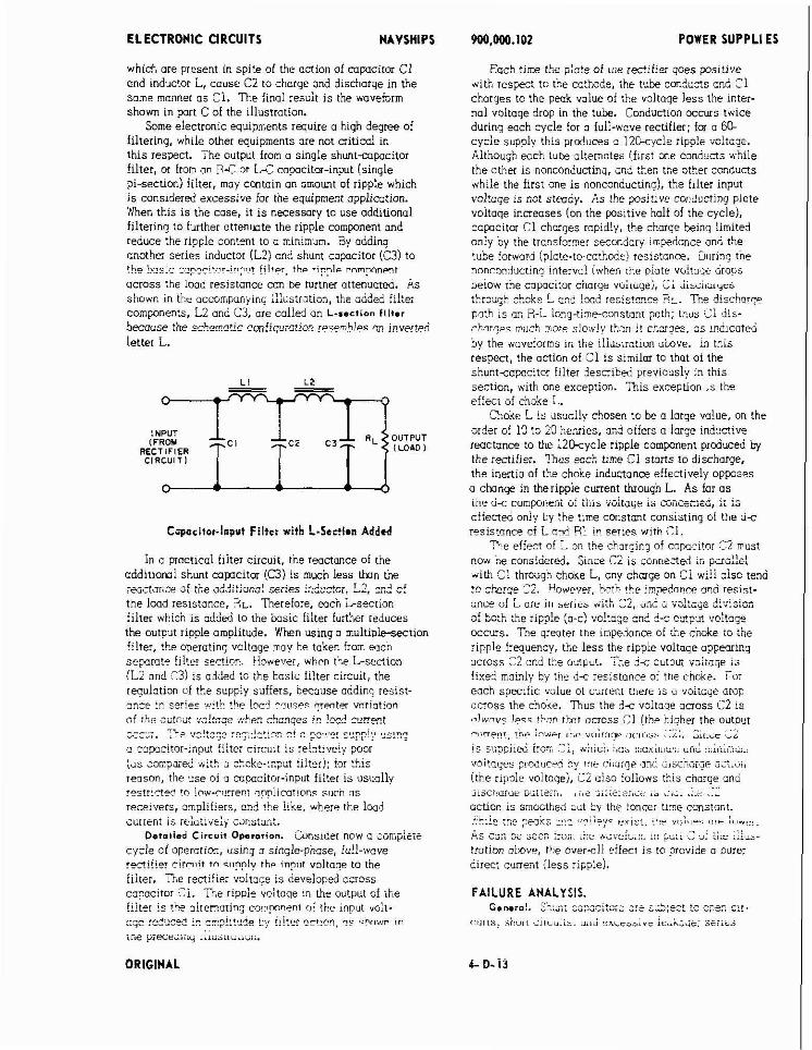
ELECTRONIC CIRCUITS NAVSHlPS
which ore present in spite of the onion of capacitor C1 and inductor L, cause C2 to charge ond discharge in the some manner as Cl. The final result i s the waveform shown in part C of the illustration.
Some electronic equipments [quire a hiqh degree o f filtering, while other equipments are not critical in this reszct . The output from o single shuntcopacitor fi!!er, m from an P C or L.-C cnpocitor-input (sinole pi-section) filter, may contain an rrmount of ripple which i s considered excessive for the equipment application. 'When this i s the cose, it i s necessary to use additional filtering to further atteninte the ripple component and reduce the ripple content to a minimum. 5y adding another series inductor (LZ) cnd shunt cnpacitor (C3) to !he ks i c c?prir!!nr4npo! !iltor, the ri??lp rnmponpnt across the load resiston= con be further attenuatffl. HS
s!lown in ti:r acciirnponjir,g ;I:ystrctio~, the odd& fi!:e; components, L2 and C3, ore called an L-section f111.r I k ~ ~ e the schematic ~m!im~~n!io~ ~eremhler ~n i"veitiYi letter L.
L I 12
INPUT (FROM OUTPUT
RECTIFIER I LOAD I CIRCUIT1
Caporitor-Input Filte: with L-Ssc?l*a Addtd
In a proct~cal fllter clrcu~t, ine reanonce of the addiuoml shunt mpocitor (C3) is much less than the reactance of :he ~dlitionz! series i.?dcctcr. L2, :c? c! the load reslstance, 3i. Therefore, eoch L-section filter wb.ich is added to the 'basic filter flirther reduces the output ripple amplitude. When using o multipiesection filter, the operotinq voltage may be taken from each s e p ~ o t e !i!ter section. However, when the L-section (L2 ond 5) is added to the basic filter ckcuit, the regulation of the supply suffers, becouse addinq resist- znze !: series .wi!b t5e !nc+ c ~ m e s 7rmtu vsriotion c! :'.r cot-;: w1:;qe -hen ckznqes in !ocdcc.?ret uL.-. . ?>,? .~2!:.7;? ~ C ~ : ! Z ! : C ? 2! c ?c?>!z: 5,2p?!y ,2Si"?
sap3citor-input fiitei rirc;llt is reictlvely poor ( z s ;am?aed wit". zkoke-:a;.u! filter); !or th:s reoson, the use of a capacitor-input filter is usually InS!r!?lev!n !ow--i!rier;t ?ppllcaflans silcn o s rece:izers, omplifieis, and the like, where the load current i s iehtivt;i CL)IIS~O~~:.
Dotalleti Circuir Dparorion. ionsldri now u iompieie cycle of operction, (using s singlephsse, lull-wove r--ti!ier rlrniit in s,~??!y the innut voltage to the filter. Tr,e rectifier vol tqe is developed across capacitor S i . Tre rippie vcitoqe in the output of the filter is the elrernr?!in.: cnm,pwnt of the mput volt- --- m A . . r - i l ." -an , , l . . i o h\, ;,it-, nrr.nn, -= <nnm ," "y- ., ..~... ..~.. ine piecedi;;? I L ~ u s ~ ~ Y L . ~ . . .
900.W0.102 POWER SUPPLIES
Each time the plate of we rectlfler qoes positive with r e spc t tc the cathode, the tube conducts and C1 charges to the peak volue of the voltaqe less the mter- nal voltage drop in the tube. Conduction occurs twice during each cycle for o full-wcve rectifier: far a 6'LL cycie supply this produces a l2Ikycle ripp!e vokoge. Although each tube olternctes (flrst m e conducts while the other is nonconductinq, on? :her, the other conducts while the first one i s nonconducting), the filter input vo!:aqe is not steady. ?.s the ps i t ive co~ducting piote voltage increases (on the posltive half of the cycle), capacitor C1 chcrqes rapidly, the chorge being limited only by the transior~er secondory irnpedonce and the tube forward (plote-to-cathode! reslstonce. Eorinc ine nnncondunin" interval (wi.en r k e ~ i a t r voltwe drops oeiow me copacitor cilorgr vuiiuge;, i i i i s i ; l u ~ r c ~ :i.:a;gh choke L cfi? 1 x 6 :OE!S!=C~ SL. Tne nd!srhnrqp path is or: R-i io~g-time-constont ?ah; thus Ji dis- r b , ~ l ; p < mil;h mare .sianiy than it ckarges. 35 lndlcated by the woveiorrns in !he iliusrrotlon h v e . !n this respect, the oction of C1 i s similar to that 01 the . . shuntsapaiccitor !!]lei described previously in this section, with one exception. This exception is the effect of choke L.
Choke L is ~sua l ly chosen to be c large value, on the order of 13 to 20 Ler~ies, an? oifers c 1 q e ind::c!ive reactance to the 12lkycle ripple component produced by the rectiiier. Thus wch time CI stons to discharge, the inertia of the choke inductance effectively oppases a ctnnqe in theripple ctment though L. As far as ihe 6 s c u m ~ ~ ~ r n t of this voiiaqe 15 mirceiirei, it i6 affected only by the tlme constant consisting of the a< resistance of L mnd A1 In zerles w:rn i l .
7
;he effect of L on the charging o! capnci!ar 'z2 nus: now be considered. Since C2 is connect& in pmol!e! uith C l through choke L, any chorge on C i will also tend to c h q e C2. %wevs, ho!h the inpeijflnw and iesist- unce of L ore irl series nit), L2, l inl 2 vokz,-s :ivi;im -' iO.L .L ". .. .,. ,.,e rip?!= (a-c! vo!tn:e cnd d-c o.*p~t 'voltcq? occurs. The greater the impedance of the choke to :he ripple frequency, the less the ripple vaitoge oppmlng ocross C2 cnd tr.e out~ut. h e ,ji ohips voitaqe is fined moinly by the d i . resistance oi tne choke. F>r eoch specific vuiue ot current there is a vsltage drop across the choke. n,us the d s voltase across C2 i s ~ C ~ V I ~ F !*FS tLnn thnr "cross C1 (the higher the output . , rllrpn,' m. :-we. 7 i . e "<,il:lrlr , , 1 : , 1 , 5 ~ ::i;. r),:,ic i L
1s s)~ppile,5 iror .v>+5> :,:;b ::;Gx~II~L,,, U~VJ ::,ini~:a..,
u@!!a~es > r M o c m ny t:le C r . a i y Inr, 2 i S C i ~ l i j i l j i i l v i r
(the rlpple voitnqei, L i also foiiaws h i s charge and . ...
. r J e r r , ,i.c iiiii-i?:,<~: r r ,:,i. ,;.< i.- action is smoothed :u! Sv the ionqei time constant. .-.,n .^" nnnyj -.,- .?nl.ol.r " r ,c , ,.,- ",s; ,,-. ; .>*?! ~ r--..- .~ . ,~ ~
A - --- ^^ --^" ...,. .._.YI. ... . . , ~ , _ . . i - .,i :: , : ! _I Lull iliC/, i . 1 - .." .lI.I,..l ... r".. _. ". ..__I trotion ~ ~ O V P , the overail effect is to provide o aurer direct current (less ripple).
FAILURE ANALYSIS. Go..ro!. L.hx: 7;j;ci:o:; ;A;%! t.2 2;s: t!!
"!ills. sisu,, cl;iuii>. ",id ,.,,,,,,,, ;,,jut, s;i;es
ORIGINAL
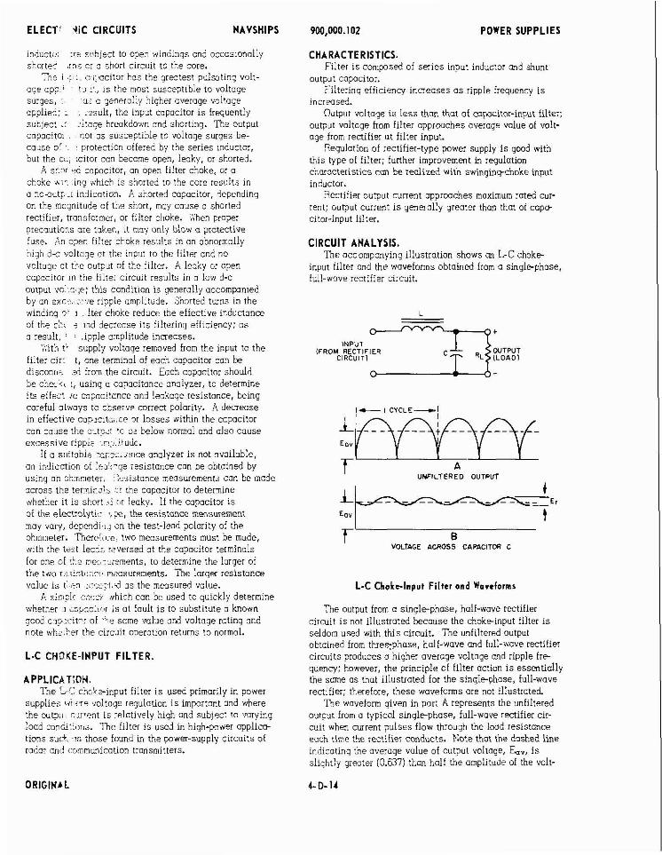
- aug paqsop aql loql aioN .s~snpuos >ag!isal aql au!l qsoa
a3ma!sal pool aql qEno~ql MOT] sas~nd lualms uaqM i~ns -11s la!]!ual anom-i[nj 'asoqdd1bu!s ps!dh~ o mo~] lndlno
pa~all!jun aql sluasaldal y llad u! uanrb UJlojaAoM aGJ -palorlsnl1! lou am slruojanoM asaql 'alojalaqi !Iag!ual
anuM-i1nj 'asoqd-alhu!s aqi lo] palonsnlI! Ioql so aums aql Ai~DJIUassa sl uO!lso IaIlrj 10 a[d!3u!1d aql 'JaAaMoq !huanb
dl] aldd!l pun afiollon aboJaAD laqb!q 0 SasnpOJd sl!n3J!s la!j!lzw aho%-lin] pm ano~-:pq 'asoqd&alql uoij pau!Dlqo
lndlno palal[!jun aqJ .i!nslp s!ql ql!~ pasn mop[as s! Jail!] indu!dyoq3 aql asnoaaq palcJlsnll! IOU s! l!rul!s
la!j!lsaJ aADM-JIDq 'asoqddihu!~ D UJOJj lndlno allJ
'l!nsl!s Ja!]!eal ahoM-Ilnj 'asoqd+lhqs D UlOl] paQDlq0 SliiJOjaADM aql pUD lall!] IildU!
dyoqs 3-7 uo SMO~S UO!IDIIS~~~! bu!hu~dwoss~ au
'SlSAlVNV 11n3813
'JJI~IJ lndu!-~ol!s ado3 jo laql uoqi Jaloalb hliolauah s1 luallns lndlno !lua~
-~ru palol unm!xom saqsoo~dda luaJln3 lndlno Ja!]!isaH 'lol3npu!
lndur ayaqs-burbu!ms ~I!M paz!pja~ aq im3 ss!e!~alsoioqs uo!lolnbal q luamanoldm! laqun] !lall!J jo adhl s!ql
~I!M pooh s! hiddns la~od adhl-~a!]!~sa~ lo uo!loln6at; 'Indq 'all!] lo ra!j!uaJ uoij aba
-1IOA 10 anpn ab~lah~ SaqSMJddo lalf!j molj ahollon jndjno
~s~a~i~wsuo~l uo!los[unmu;a.l puo >opal jo sl!n3>13 hlddns-la~od aq m pur,o] asoql .;i. '4211s SUO!I
-os!~ddo JaMOd-qb!q Ill FaSn S! Jal[!J sill. 'S:lL)',:!?11W PO01 bu!hlor, 01 lsalqns puo qb!q hlaA!iolal s! Ius~Jra wdlno aql
amqm puo luollodm! s! uo!lnjnba~ abo;lor a+rr sagddns JaMOd U! hl!lOIIJ!Jd pasn S! >all!] l!ldU!;il~ rj--y ayL
'HOliV3llddV
'10UlOU 01 Sulnlal uG!lGJado I!NJj3 aql IS;:GxqM alou puo bu!la~ abal[o~ pun anian auos st,. lo i,l:.;riL3 poob u~oq 3 atni!isqns 01 s! ~ino] lo s! lh;:a:jl3.? r :aiaqM
au!walap hlys!" 01 pasnaq ua, q3!qN J:~L: +ld~~iis v 'anp~paalnswu aql so p.,~.?::.,:' u:? :I s! anloh
muoIs!sal labrot a= 'SiuauaJnsozw ,.;:::i:i::l OMI ay 10 lab101 aqi aujulalap 01 'sluawa!-:~:au i8:i 10 auo 101 slou!uJa] ~o1!3odos aql :n paslane; ':-r-al 1s.1 aql ~ITM
'apaw aq ~snw s~uaualnsoam OM] 'xvj~~aq~ '~a~awmqo aqi 10 hl!io10d peal-lsal aqi uc i-:!puadap 'blah LOW luawamsoaw asuo>s!saJ aql 'a: '> >~1h1on3ala aqi 30
s! lol!sodos aqi j1 'Ayoal I,. lio'qs s[ I! laqlaqu autmlalap ol iol!sodas aql i: -:ru!wJai aql ssolsa
apoiu aq UC~ sluamaJnsOam ~~UOIS!S~: 'iaiammqo uo bu!sn hq pau!olqo aq uos asuolsrsa! ab~:,c:>; lo uo!lo3!pu! uo 'a1qq!0AO lou s! JazAinuo a2ll;!-.:'cl.J; ?!qol!ns a 11
. ?!dC!l an!ssa2xa asno; oslo pun ~ow~ou Mqaq ;c 3. :i'alrs aql asno; "03 ~ol!sodos aql unli!~ sass01 ic 3311'11~2idn3 an!lsaj]a u! asxuap v .hl~rn[ad uallos tihiasj: GI shomlc lnjalos hu~aq 'a>uols!saJ abnywl pun asuoirsodos a, i;aj]a sl! au!wJalap 01 '~azhjouo a3uoi!sodos o bu!sn '; ~>,sqj aq
plnoqs lol!zmdas qsa3 '1!n3l[s aql moll pz >i>uoss!p aq uos JGI!~D~D~ qs~a jo [OU~WIJI auo 'I 1a111j
aql GI lndu! aql wol$ panomal aboljon Liddns $1 ql!:), 'sasoauu! apnl!lduO aldd!' . 'ljnsal o
SD !hs"a!2~j]a h~!Jali!; Sl! aSNJ3aF pLJC ; ,,;> 341 $0
auounpu! an113ajja aql asnpa~ ayoqs Jal; i :; EUIPU[M aql u! sum1 pallous 'apnlr~dmo aldd!J a!.:,..:.>xa uo hq pa~uodmossa L1;olauab s! uo!lrpuo3 slql !a!,c ,3h lndlno
s-F MOT o U! sllnsal Ilnsirs iai11] ayl UI lol!~cdos "ado la h~cal y 'Iali!j aqi 10 lndjno aql 13 aEoljon
ou pua J~I;!] aql GI mdu! aqi 13 abolloh 3-p qE!q ,411~w~ouqc uo u! sqnsal ayods ialT!j uacc uy ai,!palold D Mo;q /.~ua Arm 11 'uaqul ax suo1lnc3ald
ladoid uaqh! 'ayoqs Jailrj io 'Jaulojsuoll 'ia!j[lsal palloqs o asnos hum '11oqs -41 10 apnl!uEow aijl uo
Eulpuadap 'lol!sodos PWIO~E ij 'UO!IOS!PU! I- ilnD9~ 0
u! sllnsaal am, a41 ol Fallocs ST qqrn bul :.TM ay0.15 o lo 'ayoqs 'al1!] "ado un '10173Cd35 3- 1~:;s ij
'palJoqs lo 'Lyw~ 'uado amosaq u33 101!51 '97 aql inq 'lolsnpui sa!las aql Aq palajjo uo!lsalold , . ,a asnos -aq sabms aEoi~oh 01 alq~ldassns so lou i~liscd03
mdmo au 'bu[l~oqs puc u#,opjjoaJq aEny : Isalqns /s~luanb3IJ S! JoI!2od33 lndu! aql 'qnS; - : :FaI[dds
aboiloh abolah3 laqb!q /,~~~latiab 3 ?n : 'sahns aEol10" GI a!qildassns lsom atii s! ',: ci !5dr aho
-~OA tti!jcspd jsa]sat aq soq 'ol!=a!'.:, . i I a'i~ .aios 341 01 I!nsi!s jmqs c ;z iur' ;alloqs
Al[~uo[so3so pus S~U[PU!M "ado oi isa!q,ii 3,: :olsnptir
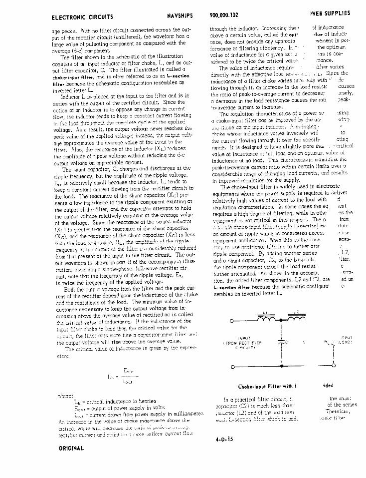
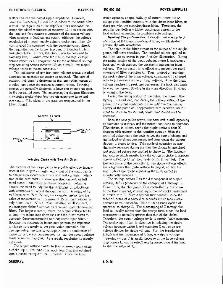
ELECTRONIC CIRCUITS NAVSHIPS
further reduces the output ripple amplitude. However, #hen the L-section, L2 and C2, i s added to the basic filter circuit, the regulotion of the supply suffers somewhat he- cause the added resistance of inductor L2 i s in series with the load and thus causes o variation of the output voltaqe when changes in load current occur. Although the voltage regulotion of o power supply using a chokeinput filter cir- cuit i s 4 (as cumcared with the copacitor-input filter), the regulotioo can be further improved if inductor L1 is o swinqinq choke. in fact, the circuit may be designed to aver-regulate, in which mse the rise in overage ~ l t o g e across copocitor CI compensates for the additional voltage drop cccwring across inductor U; a s a result, the output voltaae tends to remain mnstant
~e inductonce of any iron core inductor shows a marked decrease a s magnetic saturation i s reached. The core of ordinory inductors i s designed so that saturation occurs ot 0 value just above the moxirn~m current ratinq. Swinginq chokes are generally designed to hove one or more air gaps in the lominoted core. The accompanvinq diamam illustrates . . a swinginq choke which has two air gaps-one-large and one smoll. (?he sizes of the gaps ore exogqerated in the illustration.)
LAMINATED CORE
A SMALL AIR-
GAP
Swinging Choke with Two Air Gaps
The purpose of the lorqe gap i s to provide effective induct- ance at the largest currents, while that of the small gap i s to assure hiqh inductance at the smallest currents. Saturc- tion of the mre starts ot some specified current: at full rated current, soturotion i s almost complete. Swinging chokes are roted to indicate the variations of inductance with variotions o! current through the mil. A ratinq of 15 to 3 henries at 25 to 250 mo, for exomple, means that the value of inductance i s 15 henries 31 25 ma, and reduces to only 3 henries at 250 ma. Men handling small currents, the swinging choke functions as a mnventionol chokeinput filter. For larger currents, where the output voltage tends to drop, the inductance decreases and the filter starts to approach thechorocteristics of a copocitor-input filter. Because the decrease in inductance permits the copocitor to charge more nearly to the peak value instead of the avenge valve, the loss of voltoge in the d-c resistance of choke L2 i s thereby conpensated for, and the output voltage tends to remain constant. As a result, regulotion i s greatly improved
?he output voltage available hom a power supply using a choke-input filter circuit i s rnuch less than tho1 obtained with c copacitor-input filter. However, since the input
WO,WO.IOZ POWER SUPPLIES
choke opposes a rapid build-up of mrrent, there ore no abrupt p&-rfftifier currents with the chokeinput filter, a s there ore with the capacitor-input filtet. Thmefore, the rectifier can deliver o hiqher mntinuous current to the lood without exceeding its maximum safe ratings.
Demi1.d Circuit Opemtion. Consider now one cycle of operotim of the basic chokeinput filter, a s illustrated previously with waveforms
?he input to the filter circuit i s the output of the single- phase, full-wove rectifier. ?he rectified pulses applied to the filter are a s shown in part A of the illustration. h r i n g the rising pattion of the input voltage, choke L produces a back emf which opposes the constantly increasing input voltaqe. The net result i s to effectively prevent the rapid chorginq of filter capacitor C. Thus, instead of reaching the p& value of the input voltage, capacitor C i s charged only to the werage value of input voltage. After the input voltage reaches i ts peak and decreases, the bock emf tends to keep the current flowing in the same directloo, in effect broadening the peak.
During the rising portim of the pulse, the current flow through L i s reduced, and during the failing portion of the pulse, the current continues to rise until the diminshing enerqy of the pulse os it apprmches zero becomes insuffi- cient to maintain the current, which then commences to decrease.
When the next pulse storts, the tn& emf i s still opoosinq . . an increase in current, and thecurrent continues to decrease. (The choke, in effect, shifts the ripple peaks almost 90 degrees with respect to the rectifier output.) When the rectified pulse nears the peak value, the rate of change and the inductive effect decreases, md once again the currmt through L storts to rise. This cycle of operation i s mn- tinuously repeated during the time the circuit i s energized and rectified pulses ore applied to h o k e L T h e fluctuot- ing voltage which results ham the action of choke L appears across capacitor C and load resistor RL in parallel. The low reactance of the copocitor to this ripple voltaqe effect- ively byposses the ripple voltage to ground, so that the amplitude of the ripple voltage in the filter output i s sirylificantly reduced.
The voltaqe across C i s the d-c component or output voltage, and is produced by the charging of C through L Essentiollv. the choraina of C i s cootrolled bv the value . . , - of the time mnstant, consisting of the d-c choke resistance in series with C. Such o tvoical time m s t m t i s on the order of tenths of a s e m i or seconds rather than micro- seconds or milliseconds. Thus it takes monv mcles of opemtian to chorge C. ' h e discharging of c thkough the load i s usually slower than the charge time, since the load resistance i s normally greater than that of the choke. Therefore, the output voltage tends to remain fairly constant. The chokeinput filter i s effective in reducing the ripple voltoge because choke L and capocitor C act a s an e c voltage divider for ripple voltaqe. With the impedance of L hiqh and the impedance of C low, my ripple voltage appearing across C i s small, bemuse of the large voltoge drop ocross L, md is effectively bypassedaround the lood by the low value of X,.
ORIGINAL
ELECTRONIC CIRCUITS NAVSHIPS
FAILURE ANALYSIS. Geneml. The shunt capxitors are subject to own
circuits, short circuits, md excessive leakoge; the series inductors ore subject to open windings md, occosimolly, shorted turns or o short circuit to the core.
Shorted turns in the input choke may reduce the v a i s ot inductmce below the critical value of inductance; this will result in excessive peok-rectifier cwrent, OCCO~~M!& by m abnormally high output voltage, excessive ripple ampli- tude, md p i wltage regulation. Shorted turns in the smwthlng choke (in the mse of a multisection filter) will reduce the effective value of inductmce; this will result in less filtering efficiency, wirh m attendant increase in the output ripple amplitude. An open filter choke, or a choke ~. id i i l . : w h i r h is shnired to the core. will result in o n o output mnaltlon. k choke winring which ia siiuitei i; ::.e core m q c ~ o s e 0oee;heoting of 'l-e tubes, blown igses, etc.
The shunt capacitor(sj in the choke-input filter i s not subjected !o extrpme vnltaqe suiqes hecause of the ptorect- ion offered by the input inductor; however, the mpacitor con h m e open, lwky, or shorted. An open capacitor results in excessive ripple amplitude in the output voltage; a leaky capacitor results in a lower-thm-normd output volt- age, and a shorted capacitor resalts in a nuoutput condition.
With the supply voltage removed from the input to the filter circuit, one terminal of the capacitor can be discon- nected from the circuit. The capocitor should be checked, using o capacitance analyzer, to determine its effective capacitance and leakage resistonce. It i s important that correct polarity be observed at dl times. A decrease in eifen,ve cap"cit,,"ce or losses .*:.i:- .i,l.ll .L" Li.. i"r""..J. .- .....,, ::, , .~-; I-..
cause the filtering etficienq to decrease md produce sxcersi-:e ripp!e ompliturit?,
If o suitoble q c c i ! a ~ c e andyzer is not ovoilable, an lnalcation of leokoge resistance can be ab:&-,ii,eC by usir.; an ohmmeter. Reslstmce meosarements con be mode ~C:OSS h e terminals of the capacitor to determine whether it i s siiorred, open, or ieoky. '::hen testing electrolytic copocitorj, set the ohmmeter to the 5ig5 rmge nnd connect the test prods acioss the capacitor, being coieful to observe polarity. This is important because current ilows with !ess opposirion through an elecuoiylii copacitor in one direction thm i,n the other. I! the correct polarity i s nat observed, on incorrect reading will result. hher, me lest p r d s are first connected, a larse deflection 01 the meter !&es phre . ond then the pointer returns siowly toword the !:!!:it-P.FS p2<,11r>r! cub <he C"PUG~;G Z~IGGES. : G: Z
good copaciror wih i rutrd wu:kirrg ~okaqe ;f ? 5 ~ ~ ! : 5 , .c, :ne !!.a? relainq on jli oi,xmi;e; shs":: ui ;i: ?!I',L'Lf: ohms. ( A rouqh rule oi thumb ior high-voltage cap~citois . , . 8 . ? . - 5s 01 >mat ~ d u b onms ce; x..., - G W - , ~ : L ~ ' - - ?. - - '
tapacitars (below IUO volts mtmq; shouic na1co:e m a!r -- 6::e: z : :'-*:,,:"x 9b3:.
.. . . . ;; no aellectlaa 1s vdL2Lqe" -r: :t:e ,> t3~~e t , ? ; .A,$= ::+ ing the resistance deck explained atave, an open-circmtea capacitor is indicated.
A steady fall-scole deflectis ot the poin!er at zero oiiins ir~diictes 'La: tho ccpc-ltai ki~...~ test& is shnrt- circuited.
An iniiirotion ui u ieiikr i~Pi;;:c: i; : z:eo&; r?Ai::,; L.!! , , ~ ~ . . . . . >~.. ---- --- ,"" -,",- ," ,,.,-,;. .,,c>--L -,,.....,b. ~
ORIGINAL
9W,M10.102 POWER SUPPLIES
able value. (Be cenoin this reading is not caused by an in-circuit shunting part.) To be valid, these capacitor checks should be made with the capacitor mmpletely dismn- nected from the circuit in wnich it operates.
In highvoltage filter capocitor applications, paper md oil-filled capacitors me used, os ore d s o ~uico a d ceramic capacitors (for low-capocitonce vdues). In this case. ooioritv 1s oi no imr>o~iurl~r ~ ~ % : e s s !hi_ c~cci:Or :2:lil?!c ore marked t o r -. It is , however. q o d mainrenonce pioctlce to use the outpur polarity of thecircuit c s a wide, connecting positive to positive and negative to negative. Thus any effects of polarity on circuit tests are minimizd and the possibility of domage to components or test equiv rnent i s avoided R e m a n b n d n undischarged capacitor :e toins its po!a:ity on4 holds i ts c h q e !or ion; periods oi - . . , - L- --:- A:"& ,..me +he" ,-,,I, -;:,-,7 !?, %- .ms.s" v<,... ,,,, ,i. > " YC "".-, " _,. . , . ,,.,. .,., t h e power O F F kiore connectinq test equipment or ' i s coii-,ec:Lnq :he capacitor.
A simple in& nhict, izn be used :a r;uickly ?eterm!ce . , wnerher 3 cqacitor 1s u! I ~ L I I ! is ro ~ui.sii;u:;. 2 knri*:. qoc&copoc!ror oi iie some "due u,iii: ia::;gi- ;z';n< ;:? note whether the circuit operation returns to normal.
RESONANT FILTER.
APPLICATION. 'The resonon; iiiter i s qoire linired in i t s p l l c z t i m to
power-supply filter systems. It i s normoily used in con- junction with Ltype or pi-type filter sections, rather than by itself, since it i s designed to offer maximum cttmuotion
;.. ::.; , . ?ccect;l iiip!? !:co-ezci.. " ,.., ." ".- -I..- . .
CHARACTERISTICS. "mallel-resonant ilirer i s mmposw 01 an inGr:ts: 2.:
c cp?citor it? pmollel: seri~s-resonant :il:ei i s composed o! an inductor and G copacito: in series.
Filter i s resonant a t fundamental f r q u e n q of ripple ~.^l.",.~ ."
Pmollei-resonant filter offers maximum impedance at resonance; seriesresonant filter offers minimum impedmce at resononce.
F-. . ~,.a,,ei-ressr.w,t v ' !:It.-: r e q ~ i r i s 7ii~lsr?l 1 x 1 ;u::~o!.
ClRCUiT ~tihiYSiS. Gmetol. For specid applications where maximum at-
tenuation of the rippie trequency 1s deslrei, i: irnurzwu . . , . ?. , , . -
C-"lI..... L ' , J 5 c : ; " A . ~ , ~ .,,,:,,, :, ,;~:z";:s. :::: .... ". ." ~. . . . !i!:cr zq ;. e!t"'l.? !re p ~ n r l I j ~ ~ - r r s o n ~ n l :PI me series- . ....3 "-2 .- - : . L , " . . ~ h ." t",. i ,,,,,: ,7mpn rc; .CaU/.Y... .rill - " .. -- ~ ~~- -~ ~ . , ,wpie :;qiim,cj. Since ~b:e iiker is t;;e".on!v :c t! :~ . . , k..." ,,,.. -. . . I :,.> !,"-l,7-pn?,7! . -,< *,, .. , . - . . . - . . . . . . , , - , frequen~y l i r r i i i r t n u & a ; .sl ..I:.=. .; -. . .. . . .----- .i?..---.,,+ l i ! , ~ i, q9i,lon ,liR3 ?:. j ISe i f . i t j2, .L".^_,,, " _ .... ~. ~
co--z!l.; ;zed iz z.-i~~!i?- ~ 7 t h other !!!~PII~c secrions. A aisodvantaye oi rhe porui;r;-risufi~?: :il:e; i s :b.c: LL.e inductmce is subject to cbonge whm< t?r load olrrmr i s cnangm. Since the load currenr musr iiow L ~ ~ ~ Y u L J ; : the iir u - t o r n! the ?o;al!el-resonant !i!ter. *is current cietei- rnlnes me " d u e oi k,duc:un;e 2,;. ;jnse;jr.:!;., :!iec!: . , . , , , , , : - - -. .-- ...- - ..".... " - , , , I . I,YIL" -.."I_-
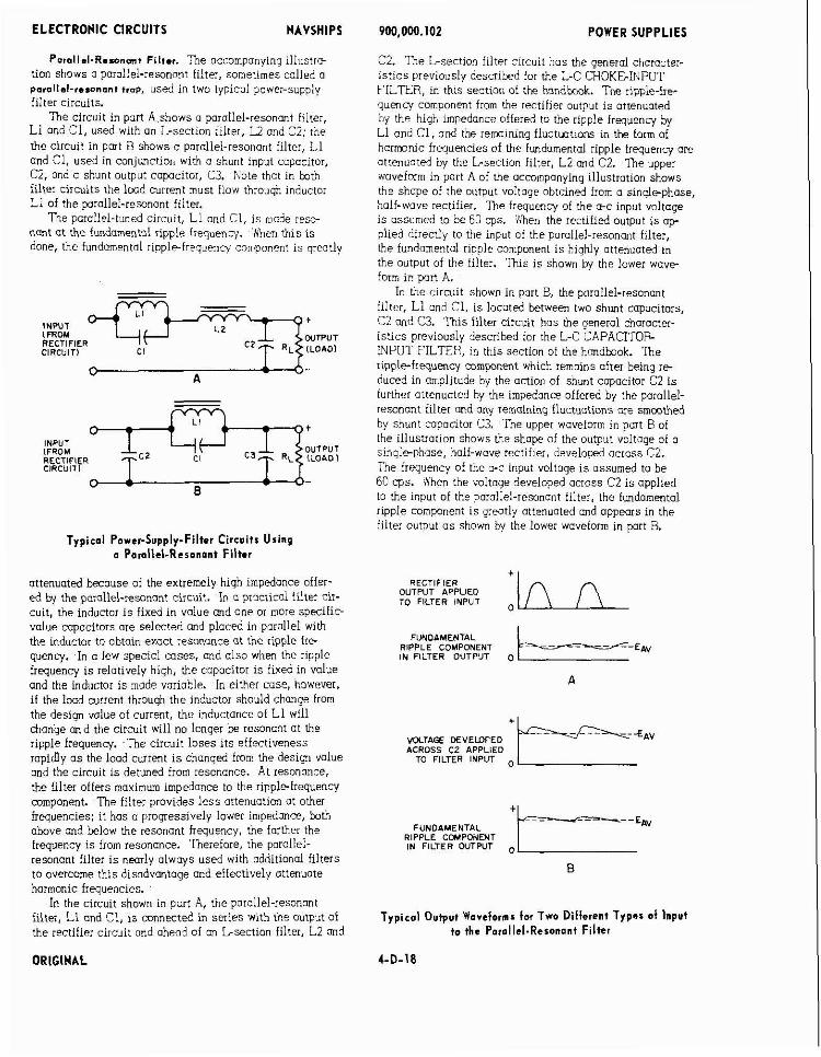
ELECTRONIC CIRCUITS NAVSHIPS
Potallsl-Rmmnmt Filter. The omomponying illustre lion shows o parollel-resonant filter, sometimes mlled o p.zrollal-resonan, trap, used in two typical power-supply filter circuits.
The circuit in port Ashows o parallel-resonant filter, L l and C1, used with on L-section filter, L2 and C2; the the circuit in port B shows a pordlel-resonant filter, L1 and Cl, used in conjunction with a shunt input capacitor, C2, and a shunt output capacitor, C3. Note that in bath filter circuits the lood current milst flow through inductor L l of the parollel-resonant filter.
The parallel-tuned circuit, L1 and Cl, is mode resw nmt at the fundamental ripple trequenq. '&hen this i s done, the fundomentol ripplpfrequenci component i s qreotly
INPUT
RECTIFIER WTPUT
CIRCUIT1
Typical Power-Supply-Filter Circuits Using a Pomllel.Rcronant Filter
attenuated hecause of the extremely high impedance offer- ed by the parollel-resonant circuit. In a practical filter cir- cuit, the inductor i s fixed in value and one or more specific- volue mpacitors ore selected and placed in pordlel with the inductor to ohtain exact resonance nt the ripple f r e quency. In a few special mses , and also when the ripple frequency i s relatively high, the copocitor i s fired in value and the inductor i s made variable. In either case, hswever, if the load current through the inductor should change from the design value of current, the inductance of L l will chonge on d the circuit will no longer be resonont at the rivole freauenni. T h e cirmit loses its effectiveness rapidly a s the iood cwrent i s changed frorr the design value ond the circuit is detuned from resonance. At resonance, the filter offers maximum impedance to the ripplefrequency component. The filter provides less attenuation at other frequencies: it has a progressively lower impedance, bath above and below the resonant frequency, the farther the frequency is from resonance. Therefore, the parallel- resonant filter i s nearly always used with odditional filters to overcome this disadvantage ond effectively ottenuote horrnonic frequencies.
In the circuit shown in port A, the parallel-resonant filter, L l and C1, is connected in s n i e s with the output of the iectifier circuit ond ahead of an Lsection filter, L2 and
ORIGINAL
900,000.102 POWER SUPPLIES
C2. The Lsection filter circuit has L+e general chorocter- ist ics previously described for the L-C CHOKEINPUT FILTER, in thls section of the handbook. The rlpple-ire- q u m q component from the rectifier output i s attenuated by the high lmpedonce offered to the ripple frequency by L1 and C l , and the iemininq fluctuations in the farm of homonic frequencies of the fundamentol ripple frequency ore attenuated by the Lsection filter, L2 ond C2. Tne upper woveform in part A of the accompanying illustrotion shows the shape of the output voltage obtained from o singlephose, holf-wove rectifier. The frequency of the a-c input voltoge is assumed to be 60 q s . '#!hen the rectified output i s a p plied directly to the input af the parallel-resonant filter, the fundamental riaple component is highly oftenvoted in the output of the filter. Tlus i s shown by the lower wove iorm in pan A.
In the circuit shown in port B, the parollel-resonant filter, L l and C1, is located between two shunt capacitors, C2 and C3. ?his filter circuit has the general charocter- istics previously described for the L-C CAPACITOR INPUT FILTER, in this section of the handhook. ?he ripplefrequency mmponent which remoins after being re- duced in amplitude by the onion of shunt capacitor C2 i s further attenuated by the impedance offered by the parallel- resonant filter and any remaining fluctuations me smoothed by shunt capacitor C3. The upper waveform in part B of the illustration shows the shape of the outpiit voltage of a singlephase, half-wave rectifier, developed across C2. 'The frequency of the a-c input voltage i s assumed to be 60 cps. bVhen the voltoge developed across C2 i s applied to the input of the parallel-resonant filter, the fundamental ripple component is qreotly ottenuoted and appears in the filter output os shown by the lower waveform in part B.
RECTIFIER OUTPUT APPLIED TO FILTER INPUT
0
FUNDAMENTAL RIPPLE COMPONENT IN FILTER OUTP'JT 0
Y O L T A a D E V E W E D ACROSS C2 APPLIED
TO FILTER INPUT
FUNDAMENTAL RIPPLE CONPWENT IN FILTER OUTPUT
TYpieol Output Waveforms for Two Different Types 01 Input to the Parollel.Reronant Filter
4-D-18
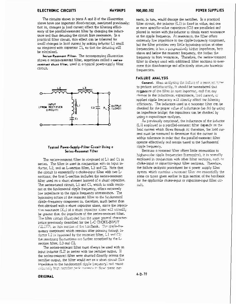
ELECTRONIC CIRCUITS
The circuits shown in parts A md B of the illustration o b v e have one important disadvontoge, mentioned previously: that is, changes in load current affect the filtering effici- ency of the parallel-resonant filter by changing the induct- ance ond thus detunina the circuit from resonance. In a pianicol filter circuit, this effect can be tolerated ior small chonaes in load current by makinq inductor L l smoll as compared wim copacltor Ci, so that the i]siuitiilg "2 : be minimized.
Series-Resonon* Filter. ' b e accompanying ilius~otion shows a series-resonmt filter, sometimes called a 'mi..- ,.son.nt .hunt filter, used in a typical power-supply filter circuiL
Typical Porer-Supply-Filter Circsit Using a Series-Resonant Filter
' h e series-resonant filter i s composed 31 L1 and C l in series. The filter i s used in conjiunction with an input irr ductor, L2, and an L-section filter, L3 and C2. Note thot the i irmit is essentiallv o chokeinput filter with t t * ~ L- sections; the first L-section includes the series-resonant filter used a s a shunt element instead of o shunt capacitor. ~- ~ ~
'hihe series-tuned circuit, L i and C i , whicin i s made resow ant ot the fundamentd ripple frequency, offers extremely low impedance to the ripple frequency atresonance. Tne bypassing onion of t+e resonant filter to the fundament;! rip~le-frequency component is, therefore, much better thm that obtained with o shunt capacitor alone, slnce the copoci. . . ti.. reactance (Xcj oi o shunt ccpacitoi done *iLi r;s;?S$ be greater thon the impedcnce of the series-resonant f~lter. -
J ne ilitei cjrcuit i;ii;suatrd :he x z e ;ene:d cham~ter- istics previously described for tke L C CKCKE-INPUT -~~ , , ---
~LLLL,-,, jn h i s sec;ion "! :!,e !,m?hk. 3.c : i ~ ! - ! e quency component whicn remains after passing tb,roagb i:? ?scrcr i 2 is bypassed by :LC :esonor.t filter, L l nnd CI; ;he remainhg flu~zuations :re !s:t5e: smmt5ed tv the L- section filter, W a n d C2
' h e series-resonant filter must always be used .uith an input inductor (L2! i n series with the rectliler output. i f the seiies-resonont filter were shunted directly across the rectifier output, the iilter wwid act os o short circuit (lva . . impedmcs to the ii;idomcn:ai :ispie i:ey~m,): i c d c%:c
. . hi-6 -n-,.:;n. ,.,, rr,l;i >,-, f] O.*. :hPSC -.I- -* ,..,.,-., ...3.. . .-.... ~ ,
ORIGINAL
POWER SUPPLIES
rents, in turn, would domoge the rectifier. in a procticol filter circuit, the inductor (L1) i s fixed in value, and one or more specifirvalue capacitors (Cl) are pmdleled ond placed in series withjheinductor to obtain exact resonance ot the ripple frequency. At resonance, the iilter offers extremely low impedance to the rlpplelrequenc~ comwnent, but the filter provides very little bypassing action at other irequencies; iI 'nus " o , " u ~ ~ --:
L>-L... :-...A""- h?+h L=a>L"=.y L...y-"-.."-,
atove ond below the resonant frequency, ine iorther iilr frequency i s from resonance. Therefore, the series-remnant filter i s always used with additional filter sections to over- come this disadvantoge ond effectively attenuate horreonic frequencies.
FAILURE ANALYSIS Gsneroi. ;?rjwj r n ~ i ~ x r . < :>,c f:iL:c c! 2 :es?x?! :!!.-?
to perform sa!is!ocmriiy, it should be remembered thot r e m c e of L!e liller i s most inpoitont, ond tho! any chonne in the inductance. cauoc~tonce, ioad current, or opplied ripple frequency will duectly oiiect tne iliterln; efficienq. The inductors used in a resonat i~i ter can be checked for the proper value of inductance (no dc) by using on impedance bridge; the capacitors can be checked by using a capacitance analyzer.
As previously mentioned, the inductance of the inductor (Ll) employed in o poiallel-resonant filter jepends i n the load current which flows through it; therefore, the load cur- rent must be meosured to determine thot the current is within tolerance in order thot the parallel-resoncmt filter operate effectively ond remain tuned to the fundamental ripple frequency.
Because o resonant filter offers little attenuation to higher-older ;ipp!e 5eqiiencie; !b,zmonics), it is normoily employed in conjunction with other filter sections, such I S
chokeinput or mpocitor-input fllter sections. 'herelore, the failure analysis procedures for a power supply filter system ,whit:? cantoins u resor!m.t fi1:e; z:e esscctiz!!;. !he some us those given earlier in lhis s e d a n of lbe handmok for the applicable choke-input or capacitor-input filter cir- cdt .
