3d-softchip: a novel architecture for next-generation adaptive computing systems
TRANSCRIPT

Hindawi Publishing CorporationEURASIP Journal on Applied Signal ProcessingVolume 2006, Article ID 75032, Pages 1–13DOI 10.1155/ASP/2006/75032
3D-SoftChip: A Novel Architecture for Next-GenerationAdaptive Computing Systems
Chul Kim,1 Alex Rassau,1 Stefan Lachowicz,1 Mike Myung-Ok Lee,2 and Kamran Eshraghian3
1 Centre for Very High Speed Microelectronic Systems, Edith Cowan University, Joondalup, WA 6027, Australia2 School of Information and Communication Engineering, Dongshin University, Naju, Chonnam 520714, South Korea3 Eshraghian Laboratories Pty Ltd, Technology Park, Bentley, WA 6102, Australia
Received 1 October 2004; Revised 15 March 2005; Accepted 25 May 2005
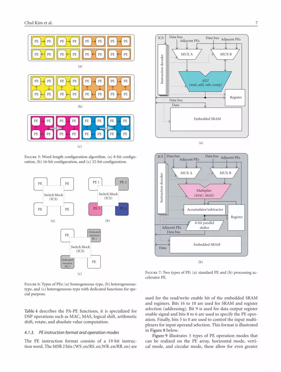
This paper introduces a novel architecture for next-generation adaptive computing systems, which we term 3D-SoftChip. The3D-SoftChip is a 3-dimensional (3D) vertically integrated adaptive computing system combining state-of-the-art processing and3D interconnection technology. It comprises the vertical integration of two chips (a configurable array processor and an intelli-gent configurable switch) through an indium bump interconnection array (IBIA). The configurable array processor (CAP) is anarray of heterogeneous processing elements (PEs), while the intelligent configurable switch (ICS) comprises a switch block, 32-bit dedicated RISC processor for control, on-chip program/data memory, data frame buffer, along with a direct memory access(DMA) controller. This paper introduces the novel 3D-SoftChip architecture for real-time communication and multimedia signalprocessing as a next-generation computing system. The paper further describes the advanced HW/SW codesign and verificationmethodology, including high-level system modeling of the 3D-SoftChip using SystemC, being used to determine the optimumhardware specification in the early design stage.
Copyright © 2006 Hindawi Publishing Corporation. All rights reserved.
1. INTRODUCTION
System design is becoming increasingly challenging as thecomplexity of integrated circuits and the time-to-marketpressures relentlessly increase. Adaptive computing is a crit-ical technology to develop for future computing systems inorder to resolve most of the problems that system design-ers are now faced with due in no small part to its potentialfor wide applicability. Up until now, however, this concepthas not been fully realized because of many technology con-straints such as chip real-estate limitations and the softwarecomplexity. With the coupled advancement of semiconduc-tor processing technology and software technology, however,adaptive computing is now facing a turning point. For in-stance, the reconfigurable computing concept has more re-cently started to receive considerable research attention [1–3]and this concept is now starting to move and expand into therealm of adaptive computing. Software defined virtual hard-ware [4] and “do-it-all” devices [5] are good examples thatdemonstrate this development direction for computing sys-tems. The major forthcoming impact from the deploymentof adaptive computing is do-it-all devices. For example, asmall handheld PDA size device could assume the function-ality of about 10 standard devices simply depending on thecontext programs included such as a cellular phone, a GPS
receiver, an MP3 player, an e-book reader, a digital camera,a portable television, a satellite radio, a handheld gamingplatform, and so forth. This concept also becomes increas-ingly important as there is a growing need for a single prod-uct to support multiple (and evolving) standards without re-engineering work.
Another growing problem in advanced computation sys-tems, particularly for real-time communication or video pro-cessing applications, is the data bandwidth necessary to sat-isfy the processing requirements. The interconnection wirerequirements in standard planar technology are increasingalmost exponentially as feature sizes continue to shrink.A novel 3D integration system such as 3D system-on-chip(SoC) [6], 3D-SoftChip [7, 8] which is able to satisfy thesevere demand of more computation throughput by effec-tively manipulating the functionality of hardware primi-tives through vertical integration of two 2D chips is anotherconcept proposed for next-generation computing systems.This paper proposes the novel 3D-SoftChip architecture asa forthcoming giga-scaled integrated circuit computing sys-tem and shows an implemented example of a single PE usingSystemC.
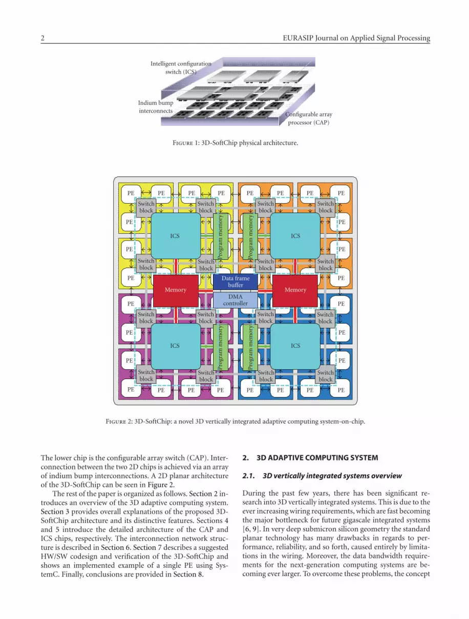
Figure 1 illustrates the physical architecture of the 3D-SoftChip comprising the vertical integration of two 2D chips.The upper chip is the intelligent configurable switch (ICS).
2 EURASIP Journal on Applied Signal Processing
Intelligent configurationswitch (ICS)
Indium bumpinterconnects
Configurable arrayprocessor (CAP)
Figure 1: 3D-SoftChip physical architecture.
Data framebuffer
Switchblock
Switchblock
Switchblock
Switchblock
Switchblock
Switchblock
Switchblock
Switchblock
Switchblock
Switchblock
Switchblock
Switchblock
Switchblock
Switchblock
Switchblock
Switchblock
DMAcontroller
ICS
ICS
ICS
ICS
Memory Memory
Pro
gram
mem
ory
Pro
gram
mem
ory
Pro
gram
mem
ory
Pro
gram
mem
ory
PE
PE
PE
PE
PE
PE
PE
PE PE PE PE PE PE PE PE
PE
PE
PE
PE
PE
PE
PEPE PE PE PE PE PE
Figure 2: 3D-SoftChip: a novel 3D vertically integrated adaptive computing system-on-chip.
The lower chip is the configurable array switch (CAP). Inter-connection between the two 2D chips is achieved via an arrayof indium bump interconnections. A 2D planar architectureof the 3D-SoftChip can be seen in Figure 2.
The rest of the paper is organized as follows. Section 2 in-troduces an overview of the 3D adaptive computing system.Section 3 provides overall explanations of the proposed 3D-SoftChip architecture and its distinctive features. Sections 4and 5 introduce the detailed architecture of the CAP andICS chips, respectively. The interconnection network struc-ture is described in Section 6. Section 7 describes a suggestedHW/SW codesign and verification of the 3D-SoftChip andshows an implemented example of a single PE using Sys-temC. Finally, conclusions are provided in Section 8.
2. 3D ADAPTIVE COMPUTING SYSTEM
2.1. 3D vertically integrated systems overview
During the past few years, there has been significant re-search into 3D vertically integrated systems. This is due to theever increasing wiring requirements, which are fast becomingthe major bottleneck for future gigascale integrated systems[6, 9]. In very deep submicron silicon geometry the standardplanar technology has many drawbacks in regards to per-formance, reliability, and so forth, caused entirely by limita-tions in the wiring. Moreover, the data bandwidth require-ments for the next-generation computing systems are be-coming ever larger. To overcome these problems, the concept

Chul Kim et al. 3
of 3D-SoC, 3D-SoftChip has been developed, which exploitsthe vertical integration of 2D planar chips to effectively ma-nipulate computation throughput. Previous work has shownthat the 3D integration of systems has a number of benefits[10]. As described by Joyner et al. [10], 3D system integrationoffers a 3.9 times increase in wire-limited clock frequency,an 84% decrease in wire-limited area, or a 25% decrease inthe number of metal levels required per stratum. There arethree feasible 3D integration methods; a stacking of pack-ages, a stacking of ICs, and a vertical system integration aswas introduced by IMEC [9]. In this research, however, thefocus is on the use of indium bump interconnection technol-ogy as indium has good adhesion, a low contact resistance,and can be readily utilized to achieve an interconnect arraywith a pitch as low as 10 µm. The development of 3D inte-grated systems will allow improvements in packaging costs,performance, reliability, and a reduction in the size of thechips.
2.2. Adaptive computing system
A reconfigurable system is one that has reconfigurable hard-ware resources that can be adapted to the application cur-rently under execution, thus providing the possibility tocustomize across multiple standards and/or applications. Inmost of the previous research in this area the concepts of re-configurable and adaptive computing have been describedinterchangeably. In this paper, however, these two conceptswill be more specifically described and differentiated. Adap-tive computing will be treated as a more extended and ad-vanced concept of reconfigurable computing. Adaptive com-puting will include more advanced software technology toeffectively manipulate more advanced reconfigurable hard-ware resources in order to support fast and seamless exe-cution across many applications. Table 1 shows the differ-ences between reconfigurable computing and adaptive com-puting.
2.3. Previous work
Adaptive computing systems are mainly classified in termsof granularity, programmability, reconfigurability, computa-tional methods, and target applications. The nature of recentresearch work in this area according to these classifications, isshown in Table 2. This table shows that the early research anddevelopment was into single linear array-type reconfigurablesystems with single and static configuration but also showsthat this has evolved towards large adaptive SoCs with het-erogeneous types of reconfigurable hardware resources andwith multiple and dynamic configurability.
As illustrated in Table 2, the 3D-SoftChip architecturehas several superiorities when compared with conventionalreconfigurable/adaptive computing systems resulting fromthe 3D vertical interconnections and the use of state-of-the-art adaptive computing technology (as will be described inthe following sections). This makes it highly suitable for thenext generation of adaptive computing systems.
3. 3D-SOFTCHIP ARCHITECTURE
3.1. Overall architecture of 3D-SoftChip
Figure 3 shows the overall architecture of the 3D-SoftChip.As can be seen, it is comprised of 4 unit chips. By includingfour separate unit chips in the architecture, sufficient flexi-bility is provided to allow multiple optimized task threads tobe processed simultaneously. Given the primary target appli-cations of multimedia processing and communications fourunit chips should be sufficient for all such requirements.Each unit chip has a PE array, a dedicated control proces-sor, and a high-bandwidth data interface unit. According toa given application program, the PE array processes largeamounts of data in parallel while the ICS controls the overallsystem and directs the PE array execution, data, and addresstransfers within the system.
3.2. Features of 3D-SoftChip
The 3D-SoftChip has 4 distinctive features: various compu-tation models, adaptive word-length configuration computa-tion [7], optimized system architecture for communication,and multimedia signal processing and dynamic reconfigura-bility for adaptive computing.
3.2.1. Computation algorithm: variouscomputation models
As described before, one 32-bit RISC controller can supplycontrol, data, and instruction addresses to 16 sets of PEsthrough the completely freely controllable switch block sovarious computation models can be achieved such asSISD,SIMD, MISD, and MIMD as required. Enough flexibility isthus achieved for an adaptive computing system. Especially,in the single instruction multiple data (SIMD) computationmodel, 3 types of different SIMD computational models canbe realized, massively parallel, multithreaded, and pipelined[19]. In the massively parallel SIMD computation model,each unit chip operates with the same global program mem-ory. Every computation is processed in parallel, maximiz-ing computational throughput. In the multithreaded SIMDcomputation model, the executed program instructions ineach unit chip can be different from the others so multi-threaded programs can be executed. The final one is the par-allel SIMD computation model. In this case each unit chipexecutes a different pipelined stage. Because of these SIMDcomputation characteristics, the 3D-SoftChip can adaptivelymaximize it’s computational throughput according to var-ious application requirements. These three computationalmodels are illustrated in Figure 4.
3.2.2. Word-length configuration
This is a key characteristic in order to classify the 3D-SoftChip as an adaptive computing system. Each PE’s basicprocessing word-length is 4 bits. This can, however, be con-figured up to 32 bits according to the application in the pro-gram memory. Figure 5 illustrates the proposed word-length

4 EURASIP Journal on Applied Signal Processing
Table 1: Reconfigurable computing versus adaptive computing.
Reconfigurable computing Adaptive computing
Hardware resourcesLinear array of homogeneous elements (logicgates, lookup tables)
Heterogeneous algorithmic elements (completefunction units such as ALU, multiplier)
ConfigurationStatic, dynamic configuration, slowreconfiguration time
Dynamic, partial runtime reconfiguration
Mapping methodsManual routing, conventional ASIC design tools(HDL)
High-level language (SystemC,C)
CharacteristicsLarge silicon area, low speed (highcapacitance), high-power consumption,high cost
Smaller silicon size, high speed, highperformance, low-power consumption,low cost
Table 2: Reconfigurable computing and adaptive computing systems.
SystemGranularity/PE-type
Programmability ReconfigurabilityComputationmethod
Target application
PADDI [11] Coarse (16 bits) Multiple Static VLIW, SIMD DSP application
MATRIX [12] Coarse (8 bits) Multiple Dynamic MIMD General purpose
RaPiD [13] Coarse (16 bits) Single Mostly static Linear array Systolic arrays
Remarc [3] Coarse (16 bits) Multiple Static SIMD Data-parallel
RAW [14] Mixed Single Static MIMD General purpose
PipeRench [1] Mixed (128 bits) Multiple Dynamic PipelinedData-parallel,DSP
MorphoSys [2] Coarse (16 bits) Multiple Dynamic SIMD Data-parallel
Triscend A7 [15] Mixed Multiple Dynamic N/A General purpose
MotorolaMRC6011[16]
Coarse (16 bits) Multiple Dynamic SIMDComputationintensiveapplication
QuickSilverAdapt2400[17]
Coarse(8, 16, 24, 32 bits)
Multiple DynamicHeterogeneousnodes array
Comm.,multimedia DSP
Elixent DFA100 [4] Coarse (4 bits) Multiple DynamicLinear D-fabricarray
Multimediaapplications
PicoChip PC102[18] Coarse (16 bits) Multiple Dynamic 3way-LIW
Wirelesscommunications
3D-SoftChip Coarse (4 bits) Multiple DynamicVarious types ofcomputationmodels
Comm., multimediasignal processing
configuration algorithm. When 2 PEs configure together, an8-bit word-length system is created. If 4 PEs configure to-gether this extends to 16 bits. And finally when 8 PEs con-figure together a full 32-bit word length is achieved. Thisflexibility is possible due to the configurable nature of thearithmetic primitives in the PEs [7, 20] and the completelyfreely controllable switch block architecture in the ICS chip.
3.2.3. Optimized system architecture for communicationand multimedia signal processing
There are many similarities between communications andmultimedia signal processing, such as data parallelism, low-precision data, and high-computation rates. The differentcharacteristics of communication signal processing are basi-cally more data reorganization, such as matrix transposition
and potentially higher bit-level computation. To fulfill thesesignal processing demands, each unit chip contains two typesof PE. One is a standard PE for generic ALU functions, whichis optimized for bit-level computation. The other is a pro-cessing accelerator PE for DSP. In addition, special address-ing modes to leverage the localized memory along with 16sets of loop buffers in the ICS add to the specialized charac-teristics for optimized communication and multimedia sig-nal processing.
3.2.4. Dynamic Reconfigurability forAdaptive Computing
Every PE contains a small quantity of local embedded SRAMmemory and additionally the ICS chip has an abundantmemory capacity directly addressable from the PEs via the

Chul Kim et al. 5
Unit chip 1
DMA
controller
Programmemory
PE
PE
PE
PE
ICS
ICS chip
CAP chipIBI IBI IBI
Dataframebuffer
Datamemory
PE array
Unit chip 2
DMA
controller
Programmemory
PE
PE
PE
PE
ICS
ICS chip
CAP chipIBI IBI IBI
Dataframebuffer
Datamemory
PE array
Unit chip 4
DMA
controller
Programmemory
PE
PE
PE
PE
ICS
ICS chip
CAP chipIBI IBI IBI
Dataframebuffer
Datamemory
PE array
Unit chip 3
DMA
controller
Programmemory
PE
PE
PE
PE
ICS
ICS chip
CAP chipIBI IBI IBI
Dataframebuffer
Datamemory
PE array
Figure 3: Overall architecture for 3D-SoftChip.
indium bump interconnect array. Multiple sets of programmemory, the abundant memory capacity, and the very high-bandwidth data interface unit makes it possible to switchprograms easily and seamlessly, even at runtime.
4. ARCHITECTURE OF CAP CHIP
The basic architecture of CAP chip is a linear array of het-erogeneous PEs. Figure 6 shows three possible architecturechoices for the PEs. The architecture in Figure 6(b) is sug-gested as the most feasible architecture for the PE in the3D-SoftChip because it has the optimum tradeoff betweenapplication-specific performance and flexibility. Examples oftype A can be seen in [1, 2, 12, 14], type B in [17], and typeC in [18]. The CAP chip has the basic role of the processingengine for the 3D-SoftChip. It manipulates large amounts ofdata at a high-computational rate using any of the three dif-ferent SIMD computation models previously described.
4.1. Two types of PEs
Figure 7 illustrates the two types of PE architecture chosen tooptimize multimedia signal processing and communicationtype applications.
4.1.1. Standard PE
The S-PE is for standard ALU functions and is also optimizedfor bit-level operation for communication signal processing.It comprises 4 sets of 19-bit registers for S-PE instructiondecoding, two multiplexers to select input operands fromthe data bus, adjacent PEs, or internal registers; a standardALU with a bit-serial multiplier, adder, subtracter, and com-parator, an embedded local SRAM and 4 sets of registers.The arithmetic primitives are scalable so as to make it pos-sible to reconfigure the word-length for specific tasks. Thescalable arithmetic primitive’s architecture is presented in[7, 20]. Moreover it can execute single-clock-cycle absolutevalue computation and comparison. Table 3 shows the func-tions of S-PE. It is suitable for bit-wise manipulation andgeneric ALU functions.
4.1.2. Processing accelerator PE
The PA-PE is dedicated specifically for digital signal pro-cessing DSP operations. It consists of 4 sets of 19-bit regis-ters for PA-PE instruction decoding, two multiplexers to se-lect input operands from the data bus, adjacent PEs or in-ternal registers, a signed 4-bit scalable parallel/parallel mul-tiplier, an accumulator/subtracter modified to enable MAC

6 EURASIP Journal on Applied Signal Processing
Program
1
Program
1
Program
1
Program
1
DMA
controller
DMA
controller
DMA
controller
DMA
controller
P
E
P
E
P
E
P
E
P
E
P
E
P
E
P
E
P
E
P
E
P
E
P
E
P
E
P
E
P
E
P
E
ICS
ICS
ICS
ICS
PE array
PE array
PE array
PE array
ICS chip
ICS chip
ICS chip
ICS chip
IBI IBI IBI IBI IBI IBI
IBI IBI IBI IBI IBI IBI
CAP chip CAP chip
CAP chip CAP chip
Unit chip 1: program 1 execution
Unit chip 4: program 1 execution
Unit chip 2: program 1 execution
Unit chip 3: program 1 execution
Data
frame
buffer
Data
frame
buffer
Data
frame
buffer
Data
frame
buffer
Datamemory
Datamemory
Datamemory
Datamemory
(a)
Program
1
Program
2
Program
4
Program
3
DMA
controller
DMA
controller
DMA
controller
DMA
controller
P
E
P
E
P
E
P
E
P
E
P
E
P
E
P
E
P
E
P
E
P
E
P
E
P
E
P
E
P
E
P
E
ICSRISC
ICSRISC
ICSRISC
ICSRISC
PE array
PE array
PE array
PE array
ICS chip
ICS chip
ICS chip
ICS chip
IBI IBI IBI IBI IBI IBI
IBI IBI IBI IBI IBI IBI
CAP chip CAP chip
CAP chip CAP chip
Unit chip 1: program 1 execution
Unit chip 4: program 4 execution
Unit chip 2: program 2 execution
Unit chip 3: program 3 execution
Data
frame
buffer
Data
frame
buffer
Data
frame
buffer
Data
frame
buffer
Datamemory
Datamemory
Datamemory
Datamemory
(b)
Program
1
Program
2
Program
4
Program
3
DMA
controller
DMA
controller
DMA
controller
DMA
controller
P
E
P
E
P
E
P
E
P
E
P
E
P
E
P
E
P
E
P
E
P
E
P
E
P
E
P
E
P
E
P
E
ICSRISC
ICSRISC
ICSRISC
ICSRISC
PE array
PE array
PE array
PE array
ICS chip
ICS chip
ICS chip
ICS chip
IBI IBI IBI IBI IBI IBI
IBI IBI IBI IBI IBI IBI
CAP chip CAP chip
CAP chip CAP chip
Unit chip 1: pipeline stage 1
Unit chip 4: pipeline stage 4
Unit chip 2: pipeline stage 2
Unit chip 3: pipeline stage 3
Data
frame
buffer
Data
frame
buffer
Data
frame
buffer
Data
frame
buffer
Datamemory
Datamemory
Datamemory
Datamemory
(c)
Figure 4: Computation algorithm: 3 types of SIMD computation models. (a) Massively parallel SIMD computation model, (b) multi-threaded SIMD computation model, and (c) pipelined SIMD computation model.
and MAS operations within one clock cycle, an 8-bit con-figurable barrel shifter, an embedded local SRAM, and 4sets of registers. Two shifters in the quad-PE can also be
configured to produce a 16-bit barrel shifter. Its distinctivefeatures are the single-clock-cycle MAC, MAS operationsand parallel-parallel multiplier to accelerate DSP operations.
Chul Kim et al. 7
PE PE PE PE PE PE PE PE
PE PE PE PE PE PE PE PE
(a)
PE PE PE PE PE PE PE PE
PE PE PE PE PE PE PE PE
(b)
PE PE PE PE PE PE PE PE
PE PE PE PE PE PE PE PE
(c)
Figure 5: Word-length configuration algorithm. (a) 8-bit configu-ration, (b) 16-bit configuration, and (c) 32-bit configuration.
Switch block(ICS)
PE PE
PE PE
(a)
Switch block(ICS)
PE 1 PE 2
PE 3 PE 4
(b)
Switch block(ICS)
PEDedicatedfunction
PE 1
Dedicatedfunction
PE 2
PE
(c)
Figure 6: Types of PEs: (a) homogeneous-type, (b) heterogeneous-type, and (c) heterogeneous-type with dedicated functions for spe-cial purpose.
Table 4 describes the PA-PE functions, it is specialized forDSP operations such as MAC, MAS, logical shift, arithmeticshift, rotate, and absolute value computation.
4.1.3. PE instruction format and operation modes
The PE instruction format consists of a 19-bit instruc-tion word. The MSB 2 bits (WS en/RS en,WR en/RR en) are
Data busAdjacent PEs
Data bus Adjacent PEsICS
MUX A MUX B
ALU(mul, add, sub, comp)
Register
Embedded SRAM
Data busData
Inst
ruct
ion
deco
der
(a)
Data busAdjacent PEs
Data bus Adjacent PEsICS
MUX A MUX B
Multiplier(MAC, MAS)
Accumulator/subtractor
8-bit parallelshifter
Register
Embedded SRAM
Data busAdjacent PEs
Data
Inst
ruct
ion
deco
der
(b)
Figure 7: Two types of PE: (a) standard PE and (b) processing ac-celerator PE.
used for the read/write enable bit of the embedded SRAMand registers. Bits 16 to 10 are used for SRAM and registerselection (addressing). Bit 9 is used for data output registerenable signal and bits 8 to 6 are used to specify the PE oper-ation. Finally, bits 5 to 0 are used to control the input multi-plexers for input operand selection. This format is illustratedin Figure 8 below.
Figure 9 illustrates 3 types of PE operation modes thatcan be realized on the PE array, horizontal mode, verti-cal mode, and circular mode, these allow for even greater

8 EURASIP Journal on Applied Signal Processing
Table 3: Standard PE functions.
Function Mnemonics
A and B AND
A or B OR
A xor B XOR
A + B ADD
A−B SUB
A × B SPMUL
A comp B COMP
|A| (Absolute value) ABS
Table 4: Processing accelerator PE functions.
Function Mnemonics
A × B PAMUL
A × B + out (t) MAC
A × B − out (t) MAS
Logical shift left LSL
Logical shift right LSR
Arithmetic shift right ASR
Rotate ROR
|A| (Absolute value) ABS
flexibility and help to maximize computational throughputaccording to the target application.
4.2. Embedded local SRAM
Each PE has a local embedded SRAM. The effective memorybandwidth is, therefore, increased dramatically by as muchas the total number of PEs, which will result in an increasein effective processing speed in many applications and allowsfor rapid dynamic context switching. Bus traffic can also bereduced because many data transmission operations can becontained within a PE. Consequently, power dissipation willalso be minimized.
4.3. Quad-PE
As previously described one quad-PE consists of two pairs ofPEs (two S-PE and two PA-PE). The quad-PE is controlledand configured by the switch block according to the controland address data from the ICS transmitted through the IBIA.Figure 10 shows the architecture of a single quad-PE.
5. ARCHITECTURE OF ICS CHIP
The ICS chip comprises the switch blocks, ICS RISC, pro-gram memory, data memory, data frame buffers, and DMAcontroller as illustrated in Figure 11. The ICS chip is a controlprocessor which controls the CAP chip via the IBIA as well asthe overall system. The ICS RISC provides control and ad-dress signals and data to the system as a whole. The switchblocks configure each PE based on the current program in-struction. The high-bandwidth data interface unit enables ef-ficient transmission of data and instructions within the sys-tem.
5.1. Switch block
The switch block provides data from/to each PE and alsoprovides instruction data to each PE. Three types of switchblocks, 6-sided, 7-sided, and 8-sided, provide optimized in-terconnections within the ICS chip. A pass-transistor designis used to optimize performance and minimize area allowinga completely free configuration for each PE.
5.2. ICS RISC
The ICS RISC is a 32-bit dedicated RISC control processor.The ICS RISC controls the execution of the PE array andprovides control and address signals to program/data mem-ory, the data frame buffers, and the DMA controller. It has a3-stage pipelinedarchitecture that includes instruction fetch(F), decode (D), and execute (E). To cope with the iterativenature of DSP arithmetic, it also has 16 sets of loop buffers soas to provide direct instruction to instruction decoding in-stead of fetching from program memory in each case. Thissignificantly reduces bus utilization allowing for improvedperformance and lower-power dissipation. Moreover 32 gen-eral purpose registers and specialized addressing modes areprovided for optimized communication and multimedia sig-nal processing.
5.3. High-bandwidth data interface unit
The high-bandwidth data interface unit allows the efficienttransfer of data within the 3D-SoftChip. Two sets of dataframe buffers and the DMA controller make it easy to trans-fer large amounts of data. Multiple sets of program memorysupport runtime program switching and, because of this dy-namic reconfiguration feature, adaptive computing is possi-ble. The data memory has a variable word width so it can eas-ily be combined to build wider/deeper memories and thus in-crease flexibility for different application programs andmul-tiple word-length computations.
6. INTERCONNECTION NETWORK
The interconnection network of the 3D-SoftChip can be bro-ken down into three hierarchical levels. The Inter-PE bus be-tween PEs in the CAP chip is the first level. This local inter-connection network has a 2D-mesh architecture providingnearest-neighbour interconnects between the PEs. The sec-ond level of the interconnection network is the switch blockarray interconnection. This supports longer interconnectionson the ICS chip but also has a basic 2D-mesh architec-ture. The last hierarchical level of interconnection is the in-dium bump interconnect array (IBIA). With the progressionof technology to ever decreasing semiconductor geometryscales, the prediction of interconnection delay as well as itsimpact on total system delay are crucial factors, introducing amajor limiting factor in overall system performance. To over-come these problems, 3D interconnection technology usingan array of indium bumps becomes very attractive because

Chul Kim et al. 9
Registerselection
WS en/RS en
WR en/RR en
SRAMen
SRAMselection
DoutRCtl
SPE OP MUX B MUX A
18 17 16 15 12 11 10 9 8 6 5 3 2 0
Registerselection
WS en/RS en
WR en/RR en
SRAMen
SRAMselection
DoutRCtl
PAPEOP
MUX B MUX A
18 17 16 15 12 11 10 9 8 6 5 3 2 0
Figure 8: PE instruction formats.
PE 0 PE 1 PE 2 PE 3
PE 4 PE 5 PE 6 PE 7
PE 8 PE 9 PE 10 PE 11
PE 12 PE 13 PE 14 PE 15
(a)
PE 0 PE 1 PE 2 PE 3
PE 4 PE 5 PE 6 PE 7
PE 8 PE 9 PE 10 PE 11
PE 12 PE 13 PE 14 PE 15
(b)
PE 0 PE 1 PE 2 PE 3
PE 4 PE 5 PE 6 PE 7
PE 8 PE 9 PE 10 PE 11
PE 12 PE 13 PE 14 PE 15
(c)
Figure 9: PE operation modes: (a) horizontal mode, (b) vertical mode, and (c) circular mode.
it supports a very high bandwidth coupled with a very lowinductance/capacitance (and thus low-power dissipation)[8]. However, any other equivalent 3D-interconnection tech-nology could also be applied to realize this interconnectionlevel within the 3D-SoftChip architecture.
6.1. Indium bump interconnection
Indium is an excellent material to use as an interconnect ma-terial due to its excellent adhesion to most metals, includ-ing aluminum, which is the metallization for the pads usedin most VLSI technologies. Indium has a low melting point,which implies a low work-hardening coefficient, allowing fordirect bonding on processed VLSI wafers. Additionally, itprovides excellent mechanical as well as electrical connectiv-ity (contact resistance < 1 mΩ per bump). Reflow techniquescan be used for flexibility and to increase the bump heightto width ratio as needed. Such techniques can also be usedto incorporate self-alignment features to the bonding pro-cess. Figure 12(a) illustrates a cut-away view of the flip-chipindium bump interconnection, a micrograph of a single in-dium bump after reflow can be seen in Figure 12(b).
7. HW/SW CODESIGN AND VERIFICATIONMETHODOLOGY
Figure 13 shows the HW/SW codesign methodology forthe 3D-SoftChip. HW/SW partitioning is being executed to
determine which functions should be implemented in hard-ware and which in software. The HW is currently being mod-eled at a system level using SystemC [21, 22] to verify func-tionality of the operation and to explore various architec-ture configurations while concurrently modeling the soft-ware in C. After that, a cosimulation and verification processwill be implemented to verify the operation and performanceof the 3D-SoftChip architecture and to decide on an opti-mal HW/SW architecture. More specifically, the SW will bea modified GNU C Compiler and Assembler. After the com-piler and assembler for ICS RISC has been finalized, a pro-gram for the implementation of the MPEG4 motion estima-tion algorithm will be developed and compiled using it. Af-ter that, object code can be produced, which can be directlyused as the input stimulus for an instruction set simulatorand system level simulation. The HW/SW verification pro-cess can be achieved through the comparison between the re-sults from instruction-level simulation and system-level sim-ulation. From this point on, the rest of the procedure can beprocessed using any conventional HW design methodology,such as full and semicustom design.
7.1. System level modeling of single PE
Figure 14 shows the single Standard PE block diagram, filestructure of SystemC modeling and the output waveform ofsystem-level modeled Standard PE.

10 EURASIP Journal on Applied Signal Processing
Data bus Adjacent PEsData bus Adjacent PEsICS
Inter PE bus
MUX A MUX B
ALU(mul, add, sub, comp)
Inter PE bus
Embedded SRAM
Data bus
Address
Inst
ruct
ion
deco
der
Data bus Adjacent PEs Data busICS
MUX A M
ALU(mul, add, sub, comp)
Embedded SRAM
Data bus
Address
Register
Inst
ruct
ion
deco
der
Data busAdjacent PEs
Data busAdjacent PEsICS
MUX A MUX B
Multiplier
(MAC, MAS)
Accumulator/subtractor
8-bit parallel
shifter
Register
Embedded SRAM
ctio
nde
code
r
Inter PE bus
Adjacent PEs Data bus Adjacent PEs
UX A MUX B
Multiplier
(MAC, MAS)
Accumulator/subtractor
8-bit parallel
shifter
Register
Embedded SRAM
Inst
ru
Data busAdjacent PEs
Data
Address
Inter PE bus
Switch block
Metalization pad
IBI
IBI
IBI
IBI
IBI
IBI
IBI
IBI
Figure 10: Quad PE.
Instructionaddress〈31 : 0〉
Instructionaddress〈31 : 0〉
Loop buffer(16× 32 bit)
Register file(32× 32 bit)
Program counter
I/O unit
Instruction data < 31 : 0 >
Instruction register
ALU & controlunit
Control signalsICS RISC
· · ·
Figure 11: Architecture of ICS RISC.

Chul Kim et al. 11
Subtrate/CAP chip
ICS chip Indium bumpsBonding pad
(a)
(b)
Figure 12: (a) 3D flip-chip indium bump interconnection and (b) indium bump interconnection: single indium bump after reflow.
HW/SWpartitioning
3D-SoftChipsystem specification
System-level modeling &architecture exploration of
3D-SoftChip using SystemC
Possibledesign specifications
H/W
*SystemC modelingsystem-level modeling forfunction/instruction verif.
& arch. exploration
ICS compilerassembler design
(modify GUN C compiler/assembler)
Program coding,assembling
(ICS assembler)
Instruction-levelsimulation
(ICS instruction setsimulator)
S/W
S/W specification
System-levelsimulation
Designverification
result checking
Optimum H/Wspecifications
Layout/circuit-level simulation
layout editor, spiceCircuit optimization
Design verificationDRC, LVS Go to foundry Chip test
Circuit optimization
HW/SWcodesign
Object codes
HW/SWcoverification
ILS results
SLS results
Figure 13: Suggested HW/SW codesign verification methodology.

12 EURASIP Journal on Applied Signal Processing
Reset
Din
Instructions
Clock
Dout
Clock
Stimulus
Standard PE
(a)
Testbench.cppInstructiondecoder.cpp ALU.cpp SRAM.cpp
Testbench.hInstructiondecoder.h ALU.h SRAM.h
Main.cpp
SystemC.h
(b)
(c)
Figure 14: System level modeling of single PE: (a) standard PE block diagram, (b) file structure of standard PE, and (c) the output waveformof system-level modeled standard PE.
8. CONCLUSIONS
A novel 3D vertically integrated adaptive computing systemarchitecture for communication and multimedia signal pro-cessing has been presented along with system-level model-ing example of a single PE. The described system leveragesthe very high-bandwidth connection between two chips, re-alizable through the indium bump interconnect array, tocombine high-level ICS and low-level CAP processing en-gines to create a next-generation adaptive computing sys-tem. The described system architecture of the 3D-SoftChipis currently being fully modeled in SystemC in order to de-termine the optimal hardware architecture. The SW designis being concurrently finalized so that the novel concept ofan adaptive system-on-chip computing system can be real-ized.
REFERENCES
[1] S. C. Goldstein, H. Schmit, M. Budiu, S. Cadambi, M. Moe,and R. R. Taylor, “PipeRench: a reconfigurable architectureand compiler,” IEEE Computer, vol. 33, no. 4, pp. 70–77, 2000.
[2] H. Singh, M.-H. Lee, G. Lu, F. J. Kurdahi, N. Bagherzadeh, andE. M. Chaves Filho, “MorphoSys: an integrated reconfigurablesystem for data-parallel and computation-intensive applica-tions,” IEEE Transactions on Computers, vol. 49, no. 5, pp. 465–481, 2000.
[3] T. Miyamori and K. Olukotun, “REMARC: reconfigurablemultimedia array coprocessor,” in Proceedings of ACM/SIGDA6th International Symposium on Field Programmable Gate Ar-rays (FPGA ’98), pp. 261–261, Monterey, Calif, USA, February1998.
[4] Elixent Limited, “The Reconfigurable Algorithm Processor,”http://www.elixent.com/products/white papers.htm.

Chul Kim et al. 13
[5] N. Tredennick and B. Shimamoto, “Special Report: do-it-alldevices,” IEEE Spectrum, pp. 37–40, December 2003.
[6] J. W. Joyner, P. Zarkesh-Ha, and J. D. Meindl, “Global in-terconnect design in a three-dimensional system-on-a-chip,”IEEE Transactions on Very Large Scale Integration (VLSI) Sys-tems, vol. 12, no. 4, pp. 367–372, 2004.
[7] S. Eshraghian, S. Lachowicz, and K. Eshraghian, “3-D verti-cally integrated configurable soft-chip with terabit computa-tional bandwidth for image and data processing,” in Proceed-ings of 10th International Conference on Mixed Design of Inte-grated Circuits and Systems (MIXDES ’03), pp. 143–148, Lodz,Poland, June 2003.
[8] A. Rassau, G. Alagoda, A. Ehrhardt, S. Lachowicz, and K.Eshraghian, “Design methodology for a 3D softchip videoprocessing architecture,” in Proceedings of 6th World Multicon-ference on Systemics, Cybernetics and Informatics (SCI ’02), pp.324–329, Orlando, Fla, USA, July 2002.
[9] IZM, “3D System Integration,” http://www.pb.izm.fhg.de/izm/015 Programms/010 R/.
[10] J. W. Joyner, R. Venkatesan, P. Zarkesh-Ha, J. A. Davis, andJ. D. Meindl, “Impact of three-dimensional architectures oninterconnects in gigascale integration,” IEEE Transactions onVery Large Scale Integration (VLSI) Systems, vol. 9, no. 6, pp.922–928, 2001.
[11] D. Chen and J. Rabaey, “PADDI: programmable arithmeticdevices for digital signal processing,” in Proceedings of IEEEWorkshop on VLSI Signal Processing, pp. 240–249, IEEE Press,San Diego, Calif, USA, November 1990.
[12] E. Mirsky and A. DeHon, “MATRIX: a reconfigurable com-puting architecture with configurable instruction distributionand deployable resources,” in Proceedings of IEEE Symposiumon FPGAs for Custom Computing Machines, pp. 157–166, NapaValley, Calif, USA, April 1996.
[13] D. C. Cronquist, C. Fisher, M. Figueroa, P. Franklin, and C.Ebeling, “Architecture design of reconfigurable pipelined dat-apaths,” in Proceedings of 20th Anniversary Conference on Ad-vanced Research in VLSI (ARVLSI ’99), pp. 23–40, Atlanta, Ga,USA, March 1999.
[14] E. Waingold, M. Taylor, D. Srikrishna, et al., “Baring it all tosoftware: raw machines,” IEEE Computer, vol. 30, no. 9, pp.86–93, 1997.
[15] Triscend Corporation, “Triscend A7S Configurable System-on-Chip Platforms,” http://www.triscend.com.
[16] Motorola Incorporation, “MRC6100: Reconfigurable Com-pute Fabric (RCF) device,” http://www.motorola.com/semi-conductors/.
[17] QuickSilver Technology Incorporation, “Adapt2400 ACM Ar-chitecture Overview”.
[18] picoChip Designs Limited, “PC102 Product Brief,” http://www.picochip.com.
[19] L. Guangming, Modeling, implementation and scalability of themorphoSys dynamically reconfigurable computing architecture,Ph.D. thesis, Electrical and Computer Engineering Depart-ment, University of California, Irvine, Calif, USA, 2000.
[20] S. Eshraghian, “Implementation of arithmetic primitives us-ing truly deep submicron technology (TDST),” Ms thesis,Edith Cowan University, Perth, Australia, 2004.
[21] Open SystemC Initiative, “The Functional Specification forSystemC 2.0,” http://www.systemc.org/.
[22] Open SystemC Initiative, “SystemC 2.0.1 Language ReferenceManual Rev 1.0,” http://www.systemc.org/.
Chul Kim received the B.S. degree in elec-tric engineering from Sunchon NationalUniversity, Korea, in 2003. He is currentlypursuing his Masters degree at the Centerfor Very High Speed Microelectronic Sys-tems, Edith Cowan University, Perth, Aus-tralia. His research interests include 3Dadaptive computing systems and platform-based SoC design for communication andmultimedia signal processing.
Alex Rassau received a Ph.D. degree in mi-croelectronics from the University of Read-ing, Reading, England in 2000. He joinedthe Centre for Very High Speed Microelec-tronic Systems at Edith Cowan University in2000 and his current research interests in-clude new adaptive computing architecturesand microphotonic systems.
Stefan Lachowicz received M.Eng.Sc. andPh.D. degrees from the Technical Univer-sity of Lodz, Poland in 1982 and 1987, re-spectively. In 1993 he joined Edith CowanUniversity as a Senior Lecturer in engineer-ing at the School of Engineering and Math-ematics and the Deputy Director of TheNational Networked Teletesting Facility forIntegrated Systems (NNTTF). His researchinterests include CMOS imagers, reconfig-urable architectures, and design for test.
Mike Myung-Ok Lee received B.S., MNS, and Ph.D. degrees fromthe Arizona State University, Tempe, U.S.A. in 1983, 1987, and1988, respectively. He is a Professor in the School of Informa-tion and Communication Engineering, Dongshin University, Ko-rea, and his current research interests include high-speed intelligentnetwork design, multimedia Optic-VLSI/ULSI design, telecommu-nication engineering, and nanobio-medical engineering.
Kamran Eshraghian received B.Tech.,M.Eng.Sc., and Ph.D. degrees from the Uni-versity of Adelaide, South Australia. In1979 he joined the Department of Elec-trical & Electronic Engineering at theUniversity of Adelaide after spending 10years with Philips Research both in Europeand Australia. He has held a number ofvisiting academic posts including Professorof Computer Science at Duke University,N.C., USA, Visiting Professor of Microelectronics and ComputerSystems at EPFL, Lausanne, Switzerland, visiting Professor ofComputer Technology at the University of Las Palmas and at theUniversity of Ulm in Germany. In 1987 he founded the Centre forGallium Arsenide VLSI Technology at the University of Adelaideand was appointed as its Director. In July 1994 he was invitedto take up the Foundation Chair of Computer, Electronics, andCommunication Engineering at Edith Cowan University to leadthe newly establish Department of Engineering. He has coau-thored 5 textbooks and served as the Editor of the Silicon SystemsEngineering series published by Prentice Hall. In 2004, he foundedEshraghian Laboratories as part of his vision for the horizontalintegration of nanochemistry and nanoelectronics with those ofbio- and photon-based technologies, thus creating a new platformfor future research and development.

Photograph © Turisme de Barcelona / J. Trullàs
Preliminary call for papers
The 2011 European Signal Processing Conference (EUSIPCO 2011) is thenineteenth in a series of conferences promoted by the European Association forSignal Processing (EURASIP, www.eurasip.org). This year edition will take placein Barcelona, capital city of Catalonia (Spain), and will be jointly organized by theCentre Tecnològic de Telecomunicacions de Catalunya (CTTC) and theUniversitat Politècnica de Catalunya (UPC).EUSIPCO 2011 will focus on key aspects of signal processing theory and
li ti li t d b l A t f b i i ill b b d lit
Organizing Committee
Honorary ChairMiguel A. Lagunas (CTTC)
General ChairAna I. Pérez Neira (UPC)
General Vice ChairCarles Antón Haro (CTTC)
Technical Program ChairXavier Mestre (CTTC)
Technical Program Co Chairsapplications as listed below. Acceptance of submissions will be based on quality,relevance and originality. Accepted papers will be published in the EUSIPCOproceedings and presented during the conference. Paper submissions, proposalsfor tutorials and proposals for special sessions are invited in, but not limited to,the following areas of interest.
Areas of Interest
• Audio and electro acoustics.• Design, implementation, and applications of signal processing systems.
l d l d d
Technical Program Co ChairsJavier Hernando (UPC)Montserrat Pardàs (UPC)
Plenary TalksFerran Marqués (UPC)Yonina Eldar (Technion)
Special SessionsIgnacio Santamaría (Unversidadde Cantabria)Mats Bengtsson (KTH)
FinancesMontserrat Nájar (UPC)• Multimedia signal processing and coding.
• Image and multidimensional signal processing.• Signal detection and estimation.• Sensor array and multi channel signal processing.• Sensor fusion in networked systems.• Signal processing for communications.• Medical imaging and image analysis.• Non stationary, non linear and non Gaussian signal processing.
Submissions
Montserrat Nájar (UPC)
TutorialsDaniel P. Palomar(Hong Kong UST)Beatrice Pesquet Popescu (ENST)
PublicityStephan Pfletschinger (CTTC)Mònica Navarro (CTTC)
PublicationsAntonio Pascual (UPC)Carles Fernández (CTTC)
I d i l Li i & E hibiSubmissions
Procedures to submit a paper and proposals for special sessions and tutorials willbe detailed at www.eusipco2011.org. Submitted papers must be camera ready, nomore than 5 pages long, and conforming to the standard specified on theEUSIPCO 2011 web site. First authors who are registered students can participatein the best student paper competition.
Important Deadlines:
P l f i l i 15 D 2010
Industrial Liaison & ExhibitsAngeliki Alexiou(University of Piraeus)Albert Sitjà (CTTC)
International LiaisonJu Liu (Shandong University China)Jinhong Yuan (UNSW Australia)Tamas Sziranyi (SZTAKI Hungary)Rich Stern (CMU USA)Ricardo L. de Queiroz (UNB Brazil)
Webpage: www.eusipco2011.org
Proposals for special sessions 15 Dec 2010Proposals for tutorials 18 Feb 2011Electronic submission of full papers 21 Feb 2011Notification of acceptance 23 May 2011Submission of camera ready papers 6 Jun 2011