25th anniversary article: colloidal quantum dot materials and devices: a quarter-century of advances
TRANSCRIPT

4986
REV
IEW
www.advmat.de
25th Anniversary Article: Colloidal Quantum Dot Materials and Devices: A Quarter-Century of Advances
Jin Young Kim , Oleksandr Voznyy , David Zhitomirsky , and Edward H. Sargent *
Colloidal quantum dot (CQD) optoelectronics offers a compelling combi-nation of low-cost, large-area solution processing, and spectral tunability through the quantum size effect. Since early reports of size-tunable light emission from solution-synthesized CQDs over 25 years ago, tremendous progress has been made in synthesis and assembly, optical and electrical properties, materials processing, and optoelectronic applications of these materials. Here some of the major developments in this fi eld are reviewed, touching on key milestones as well as future opportunities.
1 . Introduction
Colloidal quantum dots (CQDs) are nanometer-sized semi-conductor particles synthesized and suspended in the solution phase. In the last several decades, they have attracted consid-erable attention as an important new class of materials. Ever-growing interest in these materials derives from the convenient fabrication of solids directly from the solution-phase, as well as their rationally-engineered, wide-ranging spectral tunability afforded by the quantum size effect. [ 1,2 ] With unique physical and electronic properties that evolve from individual nanocrys-tals to packed nanocrystal fi lms, CQDs provide a rich platform for exploring new physical phenomena, as well as in rapid development of a wide variety of novel emerging technologies, such as thin fi lm photovoltaics, lighting solutions, and sensitive photodetectors. CQDs offer benefi ts in their solution pro-cessing, the use of inexpensive materials, and their unique chemical and physical properties that enable tunable function-ality. In fact, commercialization efforts are underway for photo-detection and implementation in light emission. The challenges of potential toxicity and long term stability are increasingly overcome through development of non-toxic materials [ 3,4 ] and using atomic layer deposition to introduce an encapsulating matrix within solid state fi lms used in devices, [ 5 ] respectively.
When the CQD size approaches the Bohr exciton radius characteristic of excitations within the corresponding bulk semiconductor, the exciton feels the effect of its fi nite-sized
© 2013 WILEY-VCH Verlag GmbH & Co. KGaA, Weinhewileyonlinelibrary.com
Dr. J. Y. Kim, Dr. O. Voznyy, D. Zhitomirsky, Prof. E. H. Sargent Department of Electrical and Computer EngineeringUniversity of Toronto 10 King’s College Road Toronto, Ontario , M5S 3G4 , Canada E-mail: [email protected]
DOI: 10.1002/adma.201301947
container. The wavelike properties of this bound electron-hole pair can no longer be neglected – as they typically are in bulk materials – and the optical and electronic properties of the CQDs can be tuned through particle size. CQDs’ small size also enables them to be manipulated in solution, since the particles can be induced to form a stable colloid in suitable solvents with the aid of bound, passivating organic molecules or ligands. This facilitates a range of solution-based materials pro-cessing methods, including spin-coating,
inkjet printing, and roll-to-roll casting. These processing tech-niques can be lower in cost, and more amenable to large-area processing, than typical vacuum-based processes employed in more traditional semiconductor materials processing.
The past few decades have witnessed an exponential growth of activity in the CQD research fi eld worldwide. This has been driven both by the exciting challenge of understanding the new science that explains their structure-composition-property rela-tionships with potential for applications, and the resultant com-mercial and societal impacts.
In this Review, we present historical highlights and major milestones in the fi eld of CQDs, touching on their synthesis, assembly, optical and electronic properties, materials pro-cessing, and optoelectronic and photovoltaic applications.
2 . The Birth of a New Field: Synthesizing a Materials Technology Platform for Large-Area and Low-Cost Optoelectronics
In the last 25 years, the successful synthesis of relatively mono-disperse semiconductor CQDs on the nanometer scale has created a foundation for new science and for a wide variety of potential applications. A vast range of physical and chemical CQD properties, such as electronic structure, exciton dynamics, and surface reactivity, are programmed via the particles’ phys-ical size, shape, and surface chemistry. This has prompted the development of rational and versatile synthetic routes to create CQDs in a controlled manner. The astonishing developments led by scientists across the fi eld are evidenced in the immense number of publications on CQDs; approximately 14,000 journal publications have been published over the last 25 years. Such incredible interest in this fi eld is marked by the fact that CQD chemistry and physics remain underexplored, and every major breakthrough paves the way for new CQD applications, such as control over majority carrier type and density, [ 6–10 ] enabling new
im Adv. Mater. 2013, 25, 4986–5010

REV
IEW
www.advmat.de
Jin Young Kim is currently a postdoctoral fellow in Prof. Edward H. Sargent's group at University of Toronto. He received his BS (1998) and MS (2000) degrees in Materials Science and Engineering from the Korea Advanced Institute of Science and Technology. He received his Ph.D. in Materials Science and Engineering
at Massachusetts Institute of Technology in 2012. He worked at Samsung Advanced Institute of Technology as a research staff member from 2002–2006. His current research interests include developing solution-processed colloidal quantum dot solar cells.
Oleksandr Voznyy received his Ph.D. in the physics of semiconductors from the Chernivtsi National University, Ukraine in 2004. He is now a research asso-ciate in the Edward S. Rogers Sr. Department of Electrical and Computer Engineering at the University of Toronto. His research interests are in com-putational physical chemistry,
surface science, and nanotechnology.
Prof. Edward H. Sargent holds the Canada Research Chair in Nanotechnology in the Edward S. Rogers Sr. Department of Electrical and Computer Engineering at the University of Toronto. He is a KAUST Investigator and a Fellow of the AAAS. He received his Ph.D. in Electrical and Computer Engineering from the University of
Toronto in 1998 and his B.S. in Engineering Physics from Queen's University in 1995.
optoelectronic device architectures leveraging p-n junctions employing a single type of CQD material. Furthermore, the development of new ligands has allowed for fabrication of fi eld-effect transistors (FETs) with record mobilities approaching 40 cm 2 /Vs. [ 11,12 ]
The role of quantization in determining molten glass’ color properties was uncovered in the 1980s, [ 13 ] the same decade in which the chemical synthesis of size-tuned CQDs in solution was fi rst mastered. From the early 1990s to present day, CQDs synthesis has been refi ned in a number of aspects: advances include organometallic synthesis in hot coordinating solvents; the hot-injection technique; improved size control, size disper-sity, and shape control; the advent of new materials systems; heterostructured particles such as core/shell CQDs and hybrid structures; synthesis via green chemistry; and increased control over, and understanding of the role of, nanoparticles’ surface chemistry.
The fi rst routes to successful CQD synthesis were based on aqueous and ionic chemistry, notably by Brus and Henglein [ 14–19 ] in the 1980s; these authors elucidated the fundamental prin-ciples governing the synthesis of CQDs, as well as the under-standing of electronic structure. Early syntheses consisted of a precipitation reaction in homogeneous aqueous solutions in the presence of surfactant-type or polymer-type stabilizers. In parallel to this one-phase synthesis, a two-phase technique was developed that used arrested precipitation of CQDs within inverse micelles formed with an amphiphilic surfactant. Here, the use of stabilizers prevented the colloids from agglomerating, and also stopped them from growing further, thereby ensuring that the particles remained suspended in solution.
Synthetic chemistry methods developed using these tech-niques were very versatile and relied on relatively simple experi-mental approaches, standard reagents, and low-temperature reactions. Less desirably, though, these precipitation reaction routes generally produced CQD populations having broad size distributions and thus poorly-defi ned absorption and lumi-nescence spectral features. Poor photoluminescence effi ciency was attributed to the low growth temperature employed, which resulted in CQDs with high defect concentrations. Researchers believed that high-quality CQDs would require highly crystal-line materials, prompting the move toward high-temperature synthetic paradigms.
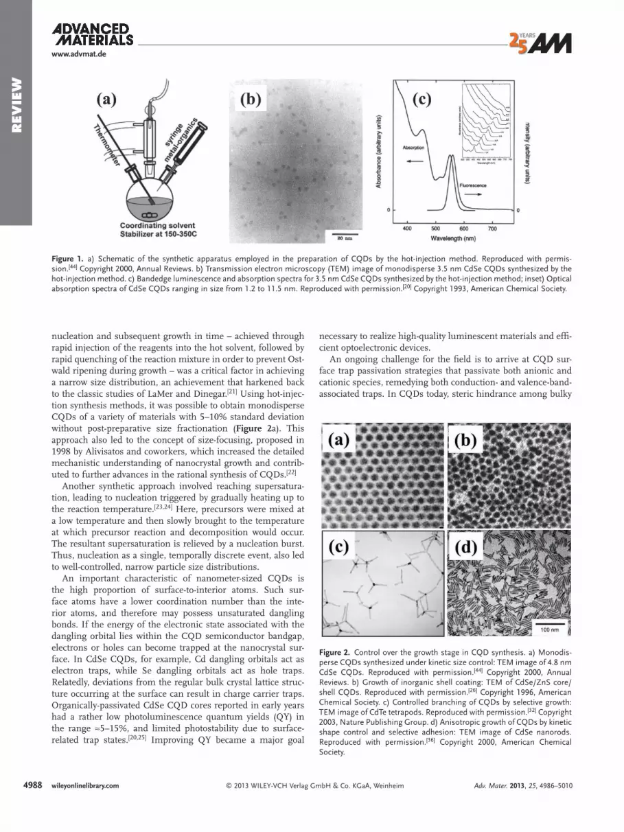
In 1993, a synthetic scheme to produce monodisperse and high-quality CQDs was presented in a landmark paper. [ 20 ] The synthesis was based on the pyrolysis of organometallic precur-sors with coordinating ligands in an organic solvent ( Figure 1 a). Cadmium chalcogenide CQDs (CdX; X = S, Se, Te) were pre-pared using dimethyl cadmium as a Cd precursor; and phos-phine selenide, phosphine telluride, or bistrimethylsilyl sulfi de as the chalcogenide source. A mixture of trioctylphosphine and trioctylphosphine oxide served as the coordinating solvent, and offered a high boiling point necessary for the high-temperature synthesis. The advance was especially notable because crys-talline, monodisperse, and highly luminescent CQDs were prepared over a signifi cant range of well-controlled and nar-rowly-distributed sizes. High reaction temperatures (≈300 °C) annealed out defects and improved crystallinity. Particle size was controlled mainly by the reaction temperature, with larger particles being obtained at higher temperatures. The average
© 2013 WILEY-VCH Verlag GAdv. Mater. 2013, 25, 4986–5010
CQD diameter was varied from ≈1 to ≈12 nm, and nanoparticle populations had a much-improved 5–10% standard deviation from the mean size (Figures 1 b and 1 c). This achievement was a milestone in the development of the synthesis of high-quality CQDs, and enabled their widespread study and application.
The introduction of rapid injection of organometallic precur-sors into an organic solvent at an elevated temperature, called the hot-injection method, was a key to the synthesis of mono-disperse CQDs. In particular, separating the two processes of
4987wileyonlinelibrary.commbH & Co. KGaA, Weinheim
498
REV
IEW
www.advmat.de
Figure 1. a) Schematic of the synthetic apparatus employed in the preparation of CQDs by the hot-injection method. Reproduced with permis-sion. [ 44 ] Copyright 2000, Annual Reviews. b) Transmission electron microscopy (TEM) image of monodisperse 3.5 nm CdSe CQDs synthesized by the hot-injection method. c) Bandedge luminescence and absorption spectra for 3.5 nm CdSe CQDs synthesized by the hot-injection method; inset) Optical absorption spectra of CdSe CQDs ranging in size from 1.2 to 11.5 nm. Reproduced with permission. [ 20 ] Copyright 1993, American Chemical Society.
Figure 2. Control over the growth stage in CQD synthesis. a) Monodis-perse CQDs synthesized under kinetic size control: TEM image of 4.8 nm CdSe CQDs. Reproduced with permission. [ 44 ] Copyright 2000, Annual Reviews. b) Growth of inorganic shell coating: TEM of CdSe/ZnS core/shell CQDs. Reproduced with permission. [ 26 ] Copyright 1996, American Chemical Society. c) Controlled branching of CQDs by selective growth: TEM image of CdTe tetrapods. Reproduced with permission. [ 32 ] Copyright 2003, Nature Publishing Group. d) Anisotropic growth of CQDs by kinetic shape control and selective adhesion: TEM image of CdSe nanorods. Reproduced with permission. [ 36 ] Copyright 2000, American Chemical Society.
nucleation and subsequent growth in time – achieved through rapid injection of the reagents into the hot solvent, followed by rapid quenching of the reaction mixture in order to prevent Ost-wald ripening during growth – was a critical factor in achieving a narrow size distribution, an achievement that harkened back to the classic studies of LaMer and Dinegar. [ 21 ] Using hot-injec-tion synthesis methods, it was possible to obtain monodisperse CQDs of a variety of materials with 5–10% standard deviation without post-preparative size fractionation ( Figure 2 a). This approach also led to the concept of size-focusing, proposed in 1998 by Alivisatos and coworkers, which increased the detailed mechanistic understanding of nanocrystal growth and contrib-uted to further advances in the rational synthesis of CQDs. [ 22 ]
Another synthetic approach involved reaching supersatura-tion, leading to nucleation triggered by gradually heating up to the reaction temperature. [ 23,24 ] Here, precursors were mixed at a low temperature and then slowly brought to the temperature at which precursor reaction and decomposition would occur. The resultant supersaturation is relieved by a nucleation burst. Thus, nucleation as a single, temporally discrete event, also led to well-controlled, narrow particle size distributions.
An important characteristic of nanometer-sized CQDs is the high proportion of surface-to-interior atoms. Such sur-face atoms have a lower coordination number than the inte-rior atoms, and therefore may possess unsaturated dangling bonds. If the energy of the electronic state associated with the dangling orbital lies within the CQD semiconductor bandgap, electrons or holes can become trapped at the nanocrystal sur-face. In CdSe CQDs, for example, Cd dangling orbitals act as electron traps, while Se dangling orbitals act as hole traps. Relatedly, deviations from the regular bulk crystal lattice struc-ture occurring at the surface can result in charge carrier traps. Organically-passivated CdSe CQD cores reported in early years had a rather low photoluminescence quantum yields (QY) in the range ≈5–15%, and limited photostability due to surface-related trap states. [ 20,25 ] Improving QY became a major goal
8 wileyonlinelibrary.com © 2013 WILEY-VCH Verlag G
necessary to realize high-quality luminescent materials and effi -cient optoelectronic devices.
An ongoing challenge for the fi eld is to arrive at CQD sur-face trap passivation strategies that passivate both anionic and cationic species, remedying both conduction- and valence-band-associated traps. In CQDs today, steric hindrance among bulky
mbH & Co. KGaA, Weinheim Adv. Mater. 2013, 25, 4986–5010

REV
IEW
organic ligands results in incomplete surface coverage and unpassivated dangling orbitals.
A major step toward the preparation of stable and highly-luminescent CQDs was taken by Hines and Guyot-Sionnest, who passivated the surface using an inorganic wider-bandgap semiconductor capping shell. [ 26 ] Overcoating CdSe CQDs with ZnS (Figure 2 b) resulted in an impressive QY of 50%. Epitaxial growth of inorganic semiconductor shells on CQD surfaces enables passivation of both anionic and cationic surface trap states, and also inhibits photo-oxidation. As photogenerated charge carriers are less likely to be trapped, the probability for excitons to decay through radiative pathways increases; CdSe/CdS and ZnSe/CdSe core/shell CQDs have since been syn-thesized that exhibit 85% and 80–90% QY, respectively. [ 27,28 ] The shell also provides a physical barrier between the optically active core and the surrounding medium, thus making the CQDs less prone to environmental infl uences, surface chem-istry, and photo-oxidation.
Early core/shell structures were mostly synthesized using a two-step procedure: initial synthesis of core CQDs, followed by a purifi cation step, and fi nally a shell growth reaction. A new strategy aiming to simplify the core/shell synthesis to a single step without intermediate purifi cation was also developed and applied to many different core/shell CQD systems such as CdSe/ZnSe, [ 29 ] CdSe/CdS, [ 27 ] and InP/ZnS. [ 30 ] Recently, core/shell growth techniques have been further refi ned to allow for precise control over shell thickness. A technique developed orig-inally for the deposition of thin fi lms onto solid substrates − suc-cessive ion layer adsorption and reaction (SILAR) − was adapted to the challenge of CQD shell growth: in 2003, Peng et al. dem-onstrated the application of the SILAR method in CdSe/CdS core/shell material synthesis, forming one monolayer at a time via alternating injection of cationic and anionic precursors. [ 31 ]
While core/shell is the most studied type of inorganic hetero-structure to date, a variety of other complex heterostructures have been developed, including a number of highly innovative shape and material combinations. Depending on the interfacial energy, lattice mismatch, and reaction conditions, multicomponent nanoscale hetrostructures have been synthesized ranging from uniformly-covered core/shells to dumbbells and even to highly anisotropic heterostructures such as tetrapods (Figure 2 c). [ 32,33 ] Using non-spherical core seeds such as nanorods and tetrapods resulted in highly anisotropic structures that could be selectively deposited on the tips of nanorods and tetrapod arms. [ 34 ]
Particularly small crystals are terminated by a variety of crystallographic facets and have a substantial numbers of surface atoms compared to atoms in bulk crystals. Thus, the energy contribution of surfaces and facets to the total energy of nanocrystals is signifi cant. Typically, the structure of a nanocrystal evolves to minimize the total product of surface area and surface energy for each facet, often producing a near-spherical structure. However, this principle applies to a system in thermodynamic equilibrium. Recognition of this notion ena-bles kinetically-controlled growth of novel, metastable nano-particles, relying on local concentrations of reacting species and the local environment in the growth medium. These insights allowed the fi eld to move beyond equilibrium spherical CQDs normally obtained in the slow growth limit under thermody-namic control. [ 35 ]
© 2013 WILEY-VCH VerlagAdv. Mater. 2013, 25, 4986–5010
www.advmat.de
The shape evolution of CQDs at any time during synthesis depends on the history of the relative growth rates of different crystal facets. The energy with which ligand molecules in the growth medium adhere to the surfaces of growing CQDs infl u-ences CQD shape evolution and growth. In a microscopic pic-ture of the growth process, the ligands dynamically bind and desorb at the nanocrystal surface, so that regions of the CQD surface are transiently accessible for growth. Strongly-adsorbed ligands retard growth, while more labile ligands enable prefer-ential growth on crystal faces to which they are adsorbed. Fur-thermore, using kinetic control in conjunction with ligands having different binding affi nity offers more effective control over CQD growth. Selective adhesion of ligand molecules allows for tuning the growth kinetics of different crystal facets and tailoring the CQD shape from nearly spherical to highly anisotropic. Thus, multicomponent mixtures of stabilizing agents are often employed to enable different growth rates in different crystallographic directions. For example, in 2000, the Peng and Alivisatos groups demonstrated that nanorod-shaped CdSe CQDs can be synthesized with the use of a mixed ligand system consisting of trioctylphosphine oxide and alkylphos-phonic acids (Figure 2 d). [ 33 ] They went onto report CdSe CQDs having a remarkable diversity of new morphologies, including arrows, pine trees, teardrops, and tetrapods. [ 36 ] The formation of these morphologies was explained through the effective monomer model and the selective adsorption of ligands on dif-ferent crystallographic faces.
Several other factors infl uence shape control in CQD syn-thesis, including monomer concentration in the growth regime, symmetry of the underlying crystal lattice, and reac-tion temperature. Judiciously controlling the replenishment of the monomer in the kinetic growth regime enables non-spherical CQD growth. For a given solution, the required monomer concentration in the reaction, to achieve particular morphologies, increases in the following order: spheres, rice grains, rods, and branched structures. [ 37–39 ] Further growth of the CQD following nucleation is also affected by the character-istic unit cell structure of the seeds, where, for example, cubic unit cells promote isotropic growth of CQDs from preformed seeds, whereas anisotropic unit cells induce anisotropic growth preferentially-oriented along crystallographically-reac-tive directions, resulting in the formation of anisotropic CQD morphologies. [ 40 ] Reaction temperature can also infl uence the crystalline phase growth of CQDs. [ 41,42 ] In cadmium chalcoge-nide systems, choosing high nucleation temperatures favors the stability of the wurtzite phase for the seed, which is pre-dominantly followed by one-dimensional growth and nanorod formation. Alternatively, at lower temperatures, zincblende nuclei are formed with characteristic tetrahedral seed geom-etry. Many semiconductor CQD materials exhibit polymor-phism – the ability to crystallize in diverse crystallographic structures such as the cubic zincblende phase or the aniso-tropic wurtzite structure. Experimental conditions program whether nucleation and growth of CQDs take place in either phase, or coexist in both phases.
The high temperature organometallic method, demon-strated for many II–VI semiconductor CQD systems, has led to a dramatic increase in the number of groups synthesizing and investigating semiconductor CQDs. Signifi cant advances
4989wileyonlinelibrary.com GmbH & Co. KGaA, Weinheim

4990
REV
IEW
www.advmat.de
have been made in tailored chemical manipulation of nano-structures, providing opportunities for continued expansion to new semiconductor CQD systems. In particular, the use of organometallic precursors and growth at a high temperature in solvents with various coordinating properties are appro-priate for the synthesis of many different II–VI, IV–VI, and III–V semiconductor CQDs. Each of these classes of materials has now been synthesized with narrow size distributions and high QYs.
Synthesis of IV–VI CQDs was realized by Murray and coworkers with the preparation of nanocrystalline PbSe. [ 43,44 ] Their method involved the reaction of trioctylphosphine sele-nide and lead oleate in diphenyl ether, leading to PbSe CQDs ranging in size from 3 to 15 nm. Further approaches were explored by chemical modifi cations, where various Pb precur-sors, including PbO and PbCl 2 , or Se precursors such as Se powder and trioctylphosphine selenide, as well as an array of solvent systems, including the non-coordinating octadecene, were employed. [ 45,46 ] Similar procedures to those developed for PbSe have been successfully adapted to yield PbTe CQDs with narrow size distributions of 5–7%. [ 47 ] Additionally, in 2003, the synthesis of PbS CQDs by the hot-injection method was fi rst reported by Hines and Scholes using the reaction of lead oleate and bistrimethylsilyl sulfi de in octadecene. [ 48 ] Subse-quent studies have also used PbO as the Pb source, and bistri-methylsilyl sulfi de in trioctylphosphine, S in octadecene, or S in oleylamine as the S source. [ 49,50 ]
A hot-injection route to III–V CQDs was also developed, principally focusing on InP and InAs. Typically, trimethylsilyl phosphine and trimethylsilyl arsine are used as the group V element source, and are injected into a hot coordinating solvent containing In or Ga sources, typically carboxylate salts. Nozik and coworkers carried out pioneering work in this regard in 1994 to synthesize InP CQDs, [ 51 ] and further improvements to the reaction system were reported by Alivisatos et al. [ 52 ] In 2002, Peng and coworkers synthesized high-quality InP and InAs CQDs using fatty acids as ligands in non-coordinating octa-decene solvents. [ 53 ]
A drawback of the traditional hot-injection method is the reliance on expensive, hazardous, and toxic organometallic pre-cursors and coordinating solvents. This realization has moti-vated many groups to develop alternative methods based on lower-cost and less hazardous chemicals. One notable trend is the shift away from pyrophoric organometallic compounds – such as dimethyl cadmium – to the use of more stable metal precursors.
In 2001, the introduction of CdO and air-stable Cd precursors for the synthesis of CdSe CQDs led to a growing movement in green synthesis of high-quality CQDs. [ 41,42 ] This was accom-plished without compromise to the unique physical properties of the CQDs prepared using earlier synthetic methods. Elimi-nating organophosphines and the use of non-hot-injection methods has the advantage of removing strongly air-sensitive chemicals from the synthesis, [ 54 ] and enables CQDs to be grown at lower synthetic temperatures (≈150 °C) via improved control over the reaction kinetics of surface ligands at the CdSe surface. [ 55 ] These steps towards a simplifi ed, robust synthesis procedure promote both enhanced reproducibility and clear avenues to reaction scale-up.
wileyonlinelibrary.com © 2013 WILEY-VCH Verlag G
3 . From Solution to Solid: Self-Assembly of Ordered Semiconductor CQD Arrays
CQD research moved rapidly beyond the synthesis of building blocks having a well-defi ned size, shape, and composition, and towards the controlled assembly of ordered structures, known as artifi cial crystals. Structures of CQDs assembled into arrays having long-range order would provide a robust foundation for designing new types of solids, predicted to exhibit novel prop-erties arising from the interactions of constituent CQDs. Such ordered arrays may exhibit superlattice effects allowing for band-like transport as opposed to hopping, greatly enhancing charge carrier mobility necessary for a host of optoelectronic applications. The fi eld provided exciting evidence of funda-mental structure-property relationships in these new types of condensed matter systems. Progress has been enabled by the combination of the availability of high-quality CQD building blocks and an enhanced understanding of the physical and chemical aspects underlying the self-assembly process. Much has been achieved since Bentzon reported self-assembled struc-tures, known as colloidal crystals, in 1989. [ 56 ]
Importantly, a high degree of uniformity in the CQD pop-ulation is necessary to produce close-packed, ordered CQD assemblies. Much like atoms or molecules that crystallize into solids, CQDs assemble into larger-scale structures that dem-onstrate various hierarchical length scales in their structure. The rational design and preparation of monodisperse CQD building blocks was crucial to systematic characterization of the structural, electronic, and optical properties of materials as they evolve from individual CQD into extended assembled structures via spontaneous or directed self-assembly processes. As the understanding of how CQDs organize into condensed matter systems has grown, so too have studies of new and col-lective phenomena in these novel condensed-phase solids.
Strategies for organization of nanoscale objects can be broadly classifi ed as either top-down methods or bottom-up methods. In top-down methods, features are written directly onto a substrate, such as via lithographic patterning. In the bottom-up approach, nanoscale building blocks are coaxed to take on the desired structure through self-assembly, and the fi nal structure is programmed by the shape, functional groups of the components, and environmental parameters. Bottom-up approaches utilize the concepts of molecular self-assembly and/or molecular recognition. From the point of view of nanomanu-facturing, these approaches offer the promise of scalability and low-cost. The desire to control, and scale, such approaches, cre-ates the pressing need for ongoing growth in the fundamental understanding of the laws that govern self-assembly of nano-structured materials.
Self-assembly is typically associated with thermodynamic equilibrium, where organized structures are characterized by a minimum in the system’s free energy. [ 57 ] Essential to self-assembly is that the building blocks organize into ordered, macroscopic structures, either through direct or indirect interactions. CQD self-assembly allows exploitation of spatial or temporal attributes of CQDs to tailor assembly formation: for example, by altering the substituents of the assembling building blocks, desirable changes in the assembly process can be achieved. Self-assembling interactions among CQDs are
mbH & Co. KGaA, Weinheim Adv. Mater. 2013, 25, 4986–5010

REV
IEW
www.advmat.de
generally dominated by attractive van der Waals and dipolar interactions, which are in turn balanced by steric/electro-static repulsion. Interdot interactions are further infl uenced by the size and shape of the CQDs and the length and molec-ular arrangement of the capping ligand shells. Moreover, the medium (e.g. solvent) also plays a complex role in the interac-tion between CQDs. This complex behavior results in kineti-cally-trapped CQDs structures, making it diffi cult to bring them into an equilibrium state. [ 58,59 ] To gain control over packing morphology, deliberate external infl uences, such as external forces or confi nement, can be introduced through a process often described as directed self-assembly. Attractively, this ena-bles the generation of patterns richer and more complex than close-packed arrays alone. Such external growth-directors affect the force balance in self-assembled structures, and therefore allow manipulation of packing geometry.
Self-assembly of CQDs can be achieved using simple methods such as evaporation-based assembly or assembly at an interface; or by more advanced methods of patterned self-assembly using lithography and micro-contact printing, where modifi cation of chemical functionalities in the patterned area leads to CQD networks programmed to grow in desired regions of a substrate.
One approach to forming CQD superlattices involves slowly evaporating the colloidal suspension onto the target substrate. Following on their earlier II–VI synthesis that pro-duced narrow size distributions of CdSe CQDs, Murray et al. crystallized CQDs into long-range-ordered structures using this technique. [ 44,60 ] Here, the extent of ordering in the close-packed CQD structure was controlled by tailoring the solvent composition to maintain stability of the CQD dispersion as the solvent evaporated, thereby leading to an increasingly concen-trated CQD solution. Examination of the evaporation kinetics revealed their strong infl uence on the self-assembly process. The solvent evaporation rate can be tuned by adjusting the vola-tility by varying the solvent composition, or by carrying out the evaporation in a slightly subsaturated vapor environment. The solvent used to deposit the CQD superlattices is also selected for its polarity, chosen so that the interaction between CQDs will become mildly attractive as the solvent evaporates and that the dispersion becomes more concentrated.
Combining two solvents in selected proportions provides an appealing and highly effective means of tuning evapora-tion rate: Murray et al. reported control over the structure of CQD fi lms prepared by drop-casting solutions of ≈8 nm CdSe CQDs coated with a trioctylphosphine oxide/trioctylphosphine mixture, and proved a strong morphological dependence on the solvent composition. [ 44 ] Tuning the ratio of octane/hexane (or octanol) solvents with different solvent volatility produced CQD assemblies exhibiting either superlattices having a high degree of order, or glassy structures possessed of a large amount of disorder.
The controlled introduction of a nonsolvent into CQD solu-tions also strongly infl uences assembly kinetics. When CQD dispersions become unstable upon introduction of a nonsol-vent, the CQDs destabilize and precipitate from solution. The aggregate structure depends on the rate of destabilization and the sticking coeffi cient between particles. [ 44 ] Fast destabilization forms low-density fractal structures as particles quickly stick
© 2013 WILEY-VCH Verlag GmAdv. Mater. 2013, 25, 4986–5010
to one another. Slowly destabilizing the dispersion, such as via slow interdiffusion among solvent and nonsolvent, results instead in close-packed superlattice structures that homoge-neously nucleate in solution. Mild destabilization provides a weakly attractive potential and suffi cient time for CQD particles to fi nd equilibrium superlattice sites. The mild destabilization method initiated by Murray and Bawendi has been augmented by the use of intermediate solvents and choice of capping ligands. [ 61,62 ]
The directed assembly of CQDs under external infl uences has also attracted much interest. Confi nement can be intro-duced to the self-assembly process at an interface via the use of substrate template, or by exerting external forces on the particle solution. Monolayer and controlled multilayer CQD assemblies have been formed by controlling the self-assembly at a liquid-air interface with Langmuir-Blodgett and Langmuir-Schaefer modifi cations, resulting in highly ordered CQD assemblies. In earlier synthetic work building on the II–VI CQD synthesis, transmission electron microscope (TEM) images of CQDs on a grid revealed appreciable two-dimensional local order. [ 20 ] Subse-quent work by that group leveraged Langmuir-Blodgett mono-layers to extend these two-dimensionally ordered domains to impressively larger (≈0.1 μ m) length scales. [ 63 ]
Langmuir CQD structures have been further engineered in a variety of novel and robust ways. Following transfer of the Langmuir monolayered structure to a patterned polydimethyl-siloxane stamp, the CQDs assembly is printed onto a substrate by bringing the stamp into contact with the surface, allowing the patterning of mono- or multilayered arrays of close-packed CQDs. [ 64 ] Interactions between the CQDs and the substrate can be exploited to template the growth of the CQD fi lm: as one example, functionalization of planar substrates with self-assembled monolayers has been applied to pattern the growth of CQD thin fi lms. [ 65 ]
Remarkably, CQD crystals can go beyond monatomic lattice types. Since the fi rst report by Kiely et al. in 1998, [ 66 ] complex binary superlattices with a number of structures have been pre-pared by employing mixtures of different types of CQDs. [ 67–70 ] When CQDs that differ in core size, ligand molecules, or core material are co-assembled, short- and long-range attractive and repulsive forces compete with sizeable entropic energy terms. Indeed, mixtures of CQDs of different sizes have very different assembly behaviors depending on the ratio between the core diameters and the ligand molecules. Three important mor-phological regimes have been observed: (1) phase separation, (2) formation of multi-particle superlattices and (3) formation of homogeneous mixtures. It is accepted that a combination of enthalpic and entropic factors leads to the formation of these structures. When the former are dominant, phase separation prevails, and when the latter are dominant, homogenous mix-tures are formed, while superlattices exist in an intermediate regime. Additionally, it has been found that CQDs have a net charge, leading to additional Coulombic attractive and repul-sive forces that need to be taken into account when studying the formation of these particle crystals. While this body of theoretical and experimental work has identifi ed the origins of these regimes, important questions remain regarding the controlled formation of fi lms having desirable optoelectronic properties. [ 67,71 ]
4991wileyonlinelibrary.combH & Co. KGaA, Weinheim

499
REV
IEW
www.advmat.de
Figure 3. Self-assembly of ordered CQD arrays. a) Optical micrograph of three-dimensional CQD crystals. These stacked crystals exhibit order over the micrometer scale and are formed by the self-organization of 2 nm CdSe CQDs. The crystals were illuminated with polarized white light and photographed with crossed polarization. Reproduced with permission. [ 60 ] Copyright 1995, American Association for the Advancement of Science. b) Scanning electron microscopy (SEM) images of three-dimensional CQD crystals of 4.8 nm CdSe CQDs. The colloidal crystal shows the characteristic pyramid shape of a <111>-oriented fcc structure. The inset shows a <100>-oriented colloidal crystals from the same sample preparation. Reproduced with permission. [ 60 ] Copyright 1995, American Association for the Advancement of Science. c) TEM image of a close-packed monolayer of 5.3 nm CdSe CQDs prepared by Langmuir-Blodgett assembly method. Reproduced with permission. [ 63 ] Copyright 1994, American Chemical Society. d) TEM image of a binary nanoparticle super-lattice self-assembled from 11 nm Fe 2 O 3 and 6 nm PbSe CQDs. Repro-duced with permission. [ 69 ] Copyright 2003, Nature Publishing Group.
Ordered CQD assemblies can be used as a powerful and versatile platform for designing two- and three-dimensional solids. Ligand-coated CQDs can be viewed as supramolecular assemblies consisting of the inorganic core coated with a three-dimensional self-assembled monolayer of ligand molecules. It is the organic monolayer coordinating each CQD surface that enables uniform CQD samples, under proper conditions, to self-assemble into CQD solids, examples of which are shown in Figure 3 . The lateral size of long-range ordered domains can be extended to the hundreds of micrometers, corresponding to astonishing order preservation and propagation on the scale of tens-of-thousands of lattice constants.
These remarkable materials are often called artifi cial solids in recognition of the similarities in their arrangements within the classic materials of solid-state physics. These analogies extend to symmetry, interdot interactions, and long-range order – and also to features of conventional crystals including faceting, twinning, polymorphism, and defects. [ 44,67,72 ] These observations suggest that CQD solids’ assembly follows fun-damental principles of crystallization analogous to the mecha-nisms that govern the formation of conventional atomic and molecular solids.
2 wileyonlinelibrary.com © 2013 WILEY-VCH Verlag G
Notwithstanding the analogies, two important structural dis-crepancies persist. Firstly, unlike atomic and molecular crys-tals where atoms, lattice geometry, and interatomic distances are well-defi ned entities, the CQD solids represent inherently polydispersed distributions of particles: in contrast with indis-tinguishable atoms, CQDs as building blocks are not absolutely identical, in spite of the fi eld’s best efforts at monodispersity. The dispersion extends beyond small variations in size and into ensemble fl uctuations in shape, composition, crystallographic orientation, and ligand coverage, producing structural inhomo-geneities among CQDs in the ensemble.
On the side of opportunity, CQD artifi cial atoms possess a greater diversity of motifs, and means of control, than atoms: not only can size and composition be infl uenced, but so too can the length and chemical functionality of the surface-bound organic monolayer, allowing tuning of the interaction poten-tials among nanoparticles and within their environment. In this regard, nanoparticles of a single family of inorganic cores represent a widely diverse set of building blocks for materials chemistry and engineering.
4 . A New Optical Material: Insights into Excited Electronic States in CQDs
CQD bandgap tunability arising from the quantum size effect inspired early applications of these materials, many of which relied on tunable photoemission properties. Single CQDs were viewed as a convenient alternative to organic dyes as markers in biological imaging [ 73 ] since they offered extended photostability and the possibility of non-resonant excitation. Other envisioned applications based on ensembles of CQDs included solution-processed light-emitting thin fi lms [ 74 ] and optical gain media for lasing applications. [ 75 ]
The physical quantity that determines the size-scale on which quantum size tunability is observed is the exciton Bohr radius – the average distance separating the electron and hole as they are bound in orbit with one another via the Coulomb interaction in bulk. Exciton Bohr radii range widely, from 1 to 50 nm, depending on the dielectric constant of the material and the charge carriers’ effective masses. [ 76 ] At sizes smaller than the exciton Bohr radius, quantum effects lead to an increased bandgap and quantized energy levels ( Figure 4 a). The extent to which bandedges shift – the quantum confi nement energy – can reach several hundreds of meV, allowing tuning of the CQD bandgap over a wide spectral range. The popularity of CdSe as a prototypical CQD material is partially due to its ability to cover the visible spectral range. Other materials, such as InAs and Pb(S, Se, Te), which posses a smaller initial bulk bandgap, can be used to extend spectral coverage into the infrared (Figure 4 b).
Another benefi t of quantization is the narrow emission linewidth, important for lasers [ 75 ] and for color reproduction in consumer applications such as displays and lighting. [ 74 ] In lighting applications, semiconducting structures favouring spatial accumulation of holes and electrons within the same volume, such as diodes in forward bias, force radiative recom-bination of carriers to occur in CQD fi lms, resulting in bright photon emission. Similarly, lasing using CQDs is possible, but
mbH & Co. KGaA, Weinheim Adv. Mater. 2013, 25, 4986–5010

REV
IEW
www.advmat.de
Figure 4. Quantum confi nement and optical properties of CQDs. a) Density of states of bulk CdSe (grey) and CdSe CQD (black) with corresponding atom-like states. b) Size-tuning of nanocrystal bandgap for different materials. Reproduced with permission. [ 73 ] Copyright 2005, American Associa-tion for the Advancement of Science. c) Absorption features of CdSe CQDs and fi ne structure of the lowest exciton. Reproduced with permission. [ 92 ] Copyright 2009, American Chemical Society.
requires optical gain through stimulated emission. These mate-rials benefi t from temperature insensitivity and reduction in the lasing threshold, but suffer from Auger recombination, which may be overcome by increasing the CQD fi ll fraction within the solid state fi lm. Efforts are underway to reduce the Auger recombination rate by using giant shell structures and smooth core-shell interface [ 77 ] and also inducing optical gain in singly excited CQDs by separating the absorption and emission wave-lengths. [ 75 ] To take advantage fully of the narrow emission prop-erty, it is important to minimize the inhomogenous broadening inherent to the CQD ensemble. Recent developments of ultra-stable magic size nanocrystals [ 78 ] and two-dimensional colloidal platelets [ 79 ] enabled ensemble linewidths as small as 45 meV, an impressive feat given that the materials are synthesized via wet chemistry. Additionally, since quantum confi nement relaxes the stringent momentum conservation rules observed in bulk sem-iconductors, materials with indirect bandgaps and poor emis-sion in bulk have been shown to become highly emitting at nanoscale sizes, with Si CQDs being a prominent example. [ 74,80 ]
Early photoluminescence decay measurements led to reports containing widely-varying lifetime values for different CQD materials, but in all cases the lifetimes were noticeably longer than the corresponding bulk values when measured at low temperature. [ 81–83 ] Since the photoluminescence QY is directly proportional to the radiative rate, understanding the origin of this slowdown was critical for applications relying on the emissive properties of CQDs. Theoretical modelling emerged as an indispensable tool in explaining these CQD properties. Early studies employed a simple particle-in-a-box model [ 84,85 ] describing the electron wavefunctions using spherical har-monics, familiar from the S, P, and D symmetries of atomic orbitals (Figure 4 a), a concept resonant with the artifi cial atom nature of CQDs. Later, more accurate k·p, [ 86,87 ] empirical pseu-dopotential, [ 88 ] and tight-binding [ 89,90 ] models took into account the underlying bandstructure and lattice structure, providing a deeper insight into the multiplicity of the excitonic transi-tions, called the exciton fi ne structure (Figure 4 c). [ 91 ] Theo-retical modelling predicted that exchange interaction splits the lowest exciton, and the spin-forbidden dark state becomes the exciton ground state in nearly all CQD systems studied, [ 87,90–93 ] explaining the reduced radiative recombination rate.
© 2013 WILEY-VCH Verlag GmAdv. Mater. 2013, 25, 4986–5010
The long radiative lifetime allows non-radiative processes, usually relaxation via phonons, to compete successfully with optical emission. At room temperature, the higher-energy, bright exciton is populated due to suffi cient thermal energy, resulting in rapid optical emission of photons from the bright state ( Figure 5 a). If, however, the dark-bright energy separa-tion is higher than the thermal energy – a situation typical for lead chalcogenides – only the dark state will be populated and the QY will degrade, as emission from the dark state is slow, thus allowing non-radiative processes to proceed. At low tem-peratures, where non-radiative decay through phonons is suf-fi ciently suppressed, QY is increased despite only the dark state being populated. [ 94,95 ]
It was soon recognized that the effi ciency and stability of nanoscale emitters, in which surface atoms comprise up to half of the entire system of atoms, is dramatically infl uenced by the quality of surface passivation. The trapped exciton, a state in which one or both carriers populate a strongly-localized surface state (Figure 5 c), is another example of a lowest-energy dark state. The wavefunction overlap of the trapped charge with that of its counterpart becomes negligible, and the desired radiative optical transition takes on a vanishing oscillator strength.
Trap states are usually associated with imperfect passiva-tion of the nanostructure surface or structural defects at the core-shell interface. Deviation of the local atomic environment from the bulk geometries – through either undercoordination or geometric distortion of the bonds – shifts atomic orbitals into the bandgap. Trap states can also form on ligand lone elec-tron pairs if they remain unbound to the surface, a situation common for facets exposing only a single dangling bond per atom. [ 96 ] Trap state formation depends on the relative alignment of the defect or lone pair level with the CQD bandedge. As one example, thiol ligands are known to quench the photolumines-cence in CdSe CQDs by introducing intragap states near the valence band; yet in CdTe, which has a smaller bandgap and thus a shallower valence bandedge, QY reaching 50% has been achieved using thiol ligands. [ 97 ] States deeper within the gap are more localized and quench the CQD emission more effectively.
Ligands that simultaneously address all classes of potential trap states will benefi t QY the most. Existing syntheses uti-lize anionic ligands that attach to cationic surface sites but are
4993wileyonlinelibrary.combH & Co. KGaA, Weinheim

499
REV
IEW
www.advmat.de
Figure 5. Role of traps in the photoluminescence QY of CQDs. a) Competition of a weak radiative transition (red) with non-radiative recombination (blue). b) Selectivity of ligand adsorption on anionic and cationic surface sites. Reproduced with permission. [ 98 ] Copyright 2010, American Chemical Society. c) Example of an atomistic simulation of a core state and surface trap. Reproduced with permission. [ 112 ] Copyright 2013, American Chemical Society. d) Effect of surface termination on the presence of surface traps. Reproduced with permission. [ 98 ] Copyright 2010, American Chemical Society.
electrostatically repelled from the electron-rich surface anions (Figure 5 b). Dangling bonds on such anions are thus particular culprits in the formation of trap states. Studies of surface ter-mination using the SILAR technique exemplify this phenom-enon, with high QY observed for cation-rich surfaces covered by ligands, and signifi cant quenching of band-to-band photo-luminescence for anion-rich, and hence ill-passivated, surfaces (Figure 5 d). [ 98,99 ]
Early studies of emission properties on the single-CQD level in 1996 revealed an unexpected new phenomenon marked by fl uorescence intermittency, often referred to as blinking, [ 100 ] reminiscent of similar observations in molecular fl uorophores. The photoluminescence of individual CQDs switches between
4 wileyonlinelibrary.com © 2013 WILEY-VCH Verlag Gm
Figure 6. Blinking of CQDs. a) Representative trace of ON and OFF states inright 2013, Royal Society of Chemistry. b) Phenomenological model of blinkindue to Auger decay of the trion or due to non-radiative recombination fromPhysical Society.
ON and OFF on timescales of seconds to minutes ( Figure 6 a). CQD blinking has no characteristic lifetime associated with the process, but instead is best-described using power-law statistics. Blinking poses a serious problem for tracking nanoparticles in bio-imaging and also causes bleaching of the CQD ensemble emission under prolonged illumination due to a higher prob-ability of the OFF than the ON states. Blinking also reduces the QY and correlates with the quality of surface passivation, sug-gesting a more complicated nature of trapping processes than previously thought, and necessitating an explanation in order to improve the QY.
Initial models of blinking were based on nanocrystals embedded in a glass matrix, [ 101 ] where blinking was ascribed
bH & Co. KGaA, Weinheim
single-CQD photoluminescence. Reproduced with permission. [ 111 ] Copy-g mechanism. Trapping of one of the carriers renders the dot OFF either trap state. Reproduced with permission. [ 107 ] Copyright 2010, American
Adv. Mater. 2013, 25, 4986–5010

REV
IEW
www.advmat.de
to Auger ionization. Given a fi nite exciton decay lifetime, there exists a chance that a second photon can be absorbed while the fi rst exciton is still present in the nanocrystal. Auger decay of the resulting biexciton provides enough energy to excite the remaining charge carrier and eject it from the nanocrystal into the surrounding matrix – or into a trap state on the CQD sur-face – while another carrier remains in the core (Figure 6 b3). As a result, every newly-created exciton now coexists with a carrier in the core from a prior excitation (Figure 6 b4). This charged exciton, called a trion, recombines non-radiatively via an Auger process on a timescale of tens of picoseconds, out-competing radiative recombination. The CQD is rendered dark for the time interval over which the charge is trapped on the surface.
Improved phenomenological models invoked different trap diffusion mechanisms, either energetic or spatial, [ 102,103 ] to randomize the trap state lifetime in order to explain the power-law statistics. These models were inspired by the experimental observation of a time-varying emission wavelength for single CQDs; a fi nding ascribed to a Stark effect resulting from an electric fi eld induced by a trapped carrier. [ 104 ] It was found that such changes in wavelength happen discretely, correlating well with the ON/OFF switching events associated with blinking. [ 105 ] The presence of multiple discrete wavelength values at which a CQD could emit therefore suggested that many traps exist on the CQD surface, capturing carriers at random.
The role of Auger recombination attracted attention from the community seeking to suppress blinking. Auger pro-cesses were also particularly important under high-intensity excitation, because of their role in quenching multiply-excited CQDs, a fact that creates an impediment to the realization of CQD lasers. [ 75 ] It was found that Auger recombination is signifi cantly enhanced in nanostructures due to increased Cou-lomb interactions between the tightly confi ned, and thus over-lapping, electron and hole. In 2010, several groups reported that despite resulting in minimal luminescence, the trion may still be brighter than the OFF state, [ 106–108 ] suggesting that a mechanism other than Auger recombination could be respon-sible for the OFF state. It was then proposed that non-radia-tive decay of the trapped exciton through phonons (Figure 6 b 3–1) is responsible for the OFF state. To explain the long OFF times, the model required the presence of multiple (up to tens of) surface traps being dynamically activated and deacti-vated at random on a long timescale. [ 109 ] The sources of this dynamic trap behavior have become the subject of the more recent studies, suggesting that there are two types of trap acti-vation, one requiring two carriers and an Auger-related process, and the other requiring only one carrier and likely diffusion-related. [ 110,111 ] Density functional theory (DFT) simulations pro-vided atomistic examples of both processes: it was shown that surface reconstructions may take place in response to charging and potentially to photoexcitation, [ 112 ] creating a trap state in a CQD that originally had none. Ligand diffusion over the sur-face has also been investigated, [ 96 ] suggesting that trap states may be formed in certain geometries visited along the diffusive trajectory, opening a pathway for trap activation-deactivation.
Complete elimination of surface traps remained a challenge, and major experimental efforts were instead directed towards decoupling the core state from the surface traps. One way to
© 2013 WILEY-VCH Verlag GmAdv. Mater. 2013, 25, 4986–5010
achieve this is to introduce a thick shell (up to 10 nm) over-coating the core, [ 113,114 ] resulting in the elimination of blinking and an increase in QY. Simultaneously, the QY of multiex-citon states was also improved owing to a signifi cantly inhib-ited Auger decay. Interestingly, even in these non-blinking CQDs, some surface traps are likely still present, resulting in weak emission intensity variations. [ 109 ] These traps, now more remote from the core state, have a much slower capture rate, effectively reducing the non-radiative recombination pathway and increasing the QY of the OFF state.
Progress in understanding and controlling blinking in CQDs marks progress in the entire CQD fi eld, since blinking depends sensitively on surface passivation and Auger pro-cesses, which are key elements in CQD-based device opera-tion. Recent achievements in CQD synthesis by the Krauss [ 115 ] and Bawendi [ 116 ] groups, both relying on high-temperature annealing, demonstrated the possibility of eliminating blinking and reaching an astounding 97% QY even in the thin-shell CQDs. These results suggest that the formation of defects at the core-shell interface was the limiting factor in QY, while close-to-ideal surface passivation is likely achievable if surface atoms are given the opportunity to move and settle down in well-coordinated confi gurations. Indeed, bulk semiconductor surfaces without ligand passivation are known to undergo surface reconstruction that attempts to adjust the fi lling of the dangling bonds and shift the resulting states away from the bandgap. [ 117 ] CQDs exhibit similar behavior, termed self-healing, [ 118 ] which strongly depends on the overall electronic balance of the CQD. [ 6,112 ] DFT simulations confi rmed that com-plete surface coverage by ligands is not required for elimina-tion of surface traps. [ 96,112 ] Traps were found to form at those rare sites suffering from severe undercoordination, and could be eliminated in simulations by sub-monolayer addition of aux-iliary cations, offering novel and diverse passivation strategies for trap elimination. [ 112 ]
A process inverse to Auger recombination, known as mul-tiple-exciton generation (MEG), has attracted much attention in CQDs. In MEG, a high-energy charge carrier scatters and expends its energy on the creation of a new electron-hole pair ( Figure 7 b), instead of a conventional energy dissipation in the form of heat (Figure 7 a). If leveraged successfully through an appropriate choice of bandgap, the process can in principle increase the power conversion effi ciency of solar cells built from CQD fi lms by ≈35% by generating more than one charge carrier for each high energy photon that is absorbed, thus increasing its contribution to the photocurrent; [ 119 ] a fact that has motivated extensive investigations of the phenomenon.
As noted by Nozik in 2002, [ 120 ] MEG is favoured in quantum confi ned systems due to the relaxation of the momentum con-servation rules and increase of Coulomb interactions between electrons and holes due to their stronger overlap; the sizeable distance among the quantized energy levels is expected to pro-duce slower phonon-mediated relaxation. The observation of MEG in CQDs reported in 2004 by Klimov, [ 121 ] was followed by studies that garnered much additional interest. [ 122 ]
Since slowing in the relaxation from levels high in the band down to the bandedge was expected to favour high MEG yields, the possibility of a phonon bottleneck in CQDs was investi-gated extensively. In contrast with what was predicted, smaller
4995wileyonlinelibrary.combH & Co. KGaA, Weinheim

49
REV
IEW
www.advmat.de
Figure 7. Multiexciton generation in CQDs. a) Conventional relaxation of an excited carrier to the bandedge through release of phonons. b) Alterna-tively, the excess carrier energy can be transferred to another exciton. c) Energy level diagram, illustrating the major processes involved in MEG: for high enough energy, relaxation of exciton through phonons competes with impact ionization, leading to formation of biexciton. The relaxed biexciton can transform back into an exciton through an inverse process called Auger recombination. Reproduced with permission. [ 129 ] Copyright 2011, American Chemical Society.
CQDs with larger intraband energy level spacings were in fact found to exhibit faster relaxation to the ground state than what was observed in larger dots, [ 123 ] suggesting that surface states and ligand vibrations were dominating the intraband relaxa-tion. [ 124 ] In 2008, special care in separating the core from the infl uence of the surface, achieved via growth of multiple shells, led to observation of the phonon bottleneck for relaxation from the 1P to the lowest-lying 1S electron state in CdSe CQDs. [ 125 ]
Early studies of MEG employed the transient absorp-tion technique, in which the dynamics of the charge carrier population residing in the lowest energy levels of the CQD are probed. In this technique, an electron excited by a high-energy pump photon quickly relaxes on a timescale of a few picoseconds to the bandedge. A delayed probe pulse, resonant with the fi rst band-to-band excitonic absorption peak, is used
96 wileyonlinelibrary.com © 2013 WILEY-VCH Verlag
Figure 8. Transient absorption spectroscopy in CQDs. a) Following photoresults in a partial bleach of absorption of a probe pulse due to state-fi llintion resonance induces 1S–1P transitions and thereby a photoinduced incrOnline Library. b) Increased pulse intensity leads to the creation of multielow intensity (black). Excitation at low intensity but at higher excitation enpermission. [ 128 ] Copyright 2007, American Chemical Society.
to assess the population of the bandedge levels by measuring the photo induced bleach in absorption ( Figure 8 a). Populating the bandedges is also accompanied by the appearance of intra-band 1S–1P transitions in the infrared (Figure 8 a). When only one exciton is present in the CQD a gradual single-exponen-tial temporal decay of the absorption bleach with the radia-tive lifetime of the exciton (≈10 ns for CdSe) is observed. As long as the CQDs in the ensemble possess, on average, well under one exciton, increasing the pump intensity will increase the bleach amplitude, but will not alter the lifetime (Figure 8 b inset). However, at higher pump intensities, it becomes pos-sible to excite two excitons per dot. In this case, a much faster component (tens of picoseconds) related to Auger recombina-tion of the biexciton is detected (Figure 8 b). [ 126 ] Triexcitons and higher-order multiexcitons exhibit proportionately faster decay
GmbH & Co. KGaA, Weinheim
excitation across the CQD bandgap, the occupation of the |1S e ,1S h > state g. Probing the same sample with pulses tuned to the fi rst intraband transi-ease in absorption. Reproduced with permission. [ 126 ] Copyright 2008, Wiley xcitons and observation of a characteristicly fast decay (red) not present at ergy results in similar signal (blue) interpreted as MEG. Reproduced with
Adv. Mater. 2013, 25, 4986–5010

REV
IEW
www.advmat.de
lifetimes. [ 127 ] Detection of MEG using the transient absorption technique was based on the observation of a fast decay, which is a signature of multiexciton presence, but done under low pump intensities ensuring that only a single photon per dot was absorbed (Figure 8 b). [ 126,128,129 ]
One challenge in using transient absorption for MEG studies is that other processes may result in similar fast-decay signatures. Photocharging due to carrier trapping on the CQD surface is one example: Auger-assisted trapping has been reported in lead chalcogenide CQDs with trapped carrier life-times on the order of seconds. [ 130 ] When additional excitation is induced in a charged dot, it coexists with the remnant carrier in the core, becoming a trion prone to fast Auger recombination. Distinguishing MEG from this trapping effect was achieved by monitoring the spectrally-resolved transient absorption [ 131 ] or the intensity of the intraband absorption (Figure 8 a) and the decay lifetime, distinguishable for the trion vs. biexciton. [ 132,133 ] A direct experimental solution employed stirring the CQDs sample, [ 129,134 ] which continuously removed any ionized CQDs from the optically probed region, and only exposed uncharged CQDs to excitation. These experiments confi rmed the presence of MEG, though led to a downward revision in its effi ciency estimation to below the 200% range. [ 133,135 ]
Proving that extra charge carriers are not simply created by MEG but can actually be separated and collected at the elec-trodes, thus improving CQD device performance, became an important milestone in MEG research. The fi rst example of successful MEG utilization in an optoelectronic device came in 2009 through the demonstration of MEG-enhanced pho-toconductive gain in CQD photodetectors. [ 136 ] In 2011 MEG was shown to improve the photovoltaic response of CQD solar cells. [ 137 ] Device modelling and comparison to experimental data suggested that more than one carrier per photon was generated for photon energies beyond 3E g but, to confi rm the MEG effect, smaller-bandgap CQD fi lms were used to shift the 3E g value closer to the energies of the solar radiation spectrum and achieve quantum effi ciency above 100% for high-energy photons.
From purely energetic considerations, MEG can occur for photon energies exceeding 2E g and proceeds further as a stair-case function with every 1E g of photon energy creating an extra exciton. In practice, currently used materials fall behind this theoretical limit due to competition with other multiexciton relaxation pathways. Improvement of MEG yield in applica-tions requires lowering the MEG threshold and exciton creation energy, prompting new materials and nanostructure designs. Theoretical models have been developed to provide a deeper understanding of the MEG process and guide material syn-thesis. [ 138–140 ] The established consensus is that the single high-energy exciton, which is not a true eigenstate of the CQD, is generated through optical absorption, and the conversion to the multiexciton competes with the phonon decay (Figure 7 c). Dif-ferent MEG effi ciencies in electronically similar PbS, PbSe and PbTe were ascribed to different couplings to phonons in these materials. [ 135 ] Since the MEG process is analogous to the impact ionization process in bulk semiconductors, [ 141 ] screening for bulk materials exhibiting high-effi ciency impact ioniza-tion provides one means of identifying materials with high MEG effi ciency potential at the nanoscale. Lead chalcogenide
© 2013 WILEY-VCH Verlag GmAdv. Mater. 2013, 25, 4986–5010
nanorods were shown to exhibit lower MEG threshold and higher effi ciency [ 135 ] due to reduced dielectric screening and thus increased Coulomb coupling. [ 142 ] Core-shell structures were recently demonstrated to exhibit even higher MEG effi ciencies.
Extensive experimental and theoretical efforts directed at understanding the physical processes on the nanoscale, com-bined with advances in materials synthesis, have enabled the development of new colloidal nanostructures with near-unity QYs, [ 116 ] reduced Auger recombination, [ 113,114 ] and enhanced multiexciton generation. [ 135 ] Utilization of these materials in optoelectronic devices demands that these properties be com-bined with effi cient electronic coupling.
5 . A New Electronic Material: Electronic Transport in Coupled Quantum Solids
The past two decades have seen advances in both the synthesis of CQDs and the formation of high-quality CQD solid-state fi lms, offering an opportunity for novel optoelectronic proper-ties and applications, such as novel device architectures and improved charge collection schemes. The goal of improving CQD device performance has driven the need for an ever-deepening understanding of the nature of charge transport in CQD solids. Foundational studies delved into charge transport properties of single CQDs, including the demonstration of a CdSe single electron transistor, [ 143 ] and scanning tunnelling microscope conductance spectroscopy that revealed the elec-tronic levels in CdSe and InAs CQDs. [ 144,145 ] Recent work has instead focused on transport in three-dimensional CQD solids; ensemble systems that will determine the performance of mac-roscale devices.
CQD solids are highly insulating if made using as-synthe-sized CQDs, possessed of long and bulky passivating ligands that result in minimal electronic wavefunction overlap among proximal CQDs. The spatial and chemical nature of inter-CQD regions can either promote or inhibit coupling, and thus impacts electron (hole) transfer to an adjacent dot. [ 146,147 ] Understanding and controlling the coupling between CQDs in the solid state has been an important avenue for the fi eld, one that has led to major strides in charge transport properties in CQD solids.
Early conductivity studies of CQD fi lms were performed primarily on CdSe CQD solids passivated using trioctylphos-phine or trioctylphosphine oxide ligands. Layered sandwich-type and inverted FET structures were used. [ 148,149 ] A very low dark conductivity (≈10 −14 S/cm) and slow decay of current in the close-packed CQD fi lms was observed in these studies. The long aliphatic barriers between cores (≈1.1 nm) and the large densities of deep traps within the fi lm – densities of approxi-mately one trap state per hundred CQDs – account for these fi ndings. [ 150 ] Because the charge carrier density in these fi lms was low, studies of transport in CdSe CQDs often relied on photoconductivity measurement by charge generation through photoexcitation.
Photoconductivity in fi lms of as-synthesized CdSe CQDs was studied by Bawendi and coworkers, who developed a model based on temperature- and electric-fi eld-dependence. [ 151 ] The
4997wileyonlinelibrary.combH & Co. KGaA, Weinheim

4998
REV
IEW
www.advmat.de
Figure 9. Thermal annealing and charge transport in CdSe CQD solids. TEM images of 6.1 nm CdSe CQD solids: a,b) as-deposited (a), and after annealing in forming gas at 350 °C (b). The interdot spacings found from these data are ≈1.1 nm for (a) and ≈0.5 nm for (b). c) Current-voltage curves of a 4.9 nm CdSe CQD solid at 77K in the dark (top) and during illumination (bottom). Curves labeled I–III are for the as-prepared fi lm, and after annealing at 110 °C and 300 °C, respectively. Reproduced with permission. [ 153 ] Copyright 2002, American Institute of Physics.
photocurrent spectra matched features within the bandedge absorption spectrum, proving that the photogenerated car-riers result from generation of quantum-confi ned electron-hole pairs. The work also offered an early picture of photoexciton ionization, a highly voltage-dependent process used to account for the highly voltage-dependent behaviour of the measured photocurrent. With increasing temperature, the photocon-ductivity decreased, without a change in the shape of the cur-rent-voltage curve. This was attributed to increased non-radi-ative recombination rate at higher temperatures, leading to a decrease in the exciton ionization effi ciency for a given voltage. Additionally, it was found that the photocurrent increased lin-early with illumination intensity, consistent with electron-hole pairs recombining with charge carriers in the fi lm.
Early transport studies revealed weak interdot coupling among adjacent CQDs, with excitations largely confi ned to indi-vidual CQDs. As a result, enhancing fi lm conductivity became a priority. Thermal annealing and chemical treatments brought CQD cores closer together, facilitating more effi cient charge transfer. [ 152 ] Doping, when used in tandem with chemical treat-ments, increased fi lm conductivity by orders of magnitude, especially when done in an electrochemical cell in which trap sites on CQDs are passivated by an inert electrolyte solution.
The thermal annealing efforts included early work by Drndic et al. on the effect of thermal annealing on electrical transport of trioctylphosphine oxide-capped CdSe CQD fi lms after deposition. [ 153 ] Annealing produced three changes: decreased separation among CQDs ( Figure 9 a); a red-shifted and broadened excitonic peak in absorption; and signifi cantly enhanced dark current and photocurrent. The dark current increased roughly 400-fold, consistent with a model in which tunnelling probability is proportional to exp (- α d ), where α −1 ≈ 0.1 nm for alkane molecules and d is the distance between the edges of the nanoparticles. [ 151 ] The photocurrent, particularly at low electric fi elds, increased by three orders of magnitude (Figure 9 b), suggesting that sensitization (e.g. photoconduc-tivity-enhancing trap states), in addition to transport, had been impacted by annealing. PbSe fi lms showed similar trends, the system evolving from an insulating regime dominated by Cou-lomb blockades to a semiconducting regime in which hopping
wileyonlinelibrary.com © 2013 WILEY-VCH Verlag G
conduction dominated transport and produced a concomitant increase in conductivity.
A drawback of the annealing strategy was that CQDs are prone to sinter, producing severe degradation in the defi nition of the absorption spectrum features. In the limit of high tem-perature annealing, this approach risked compromising the size-effect tunability of CQD solids, essentially reducing them to bulk semiconductors. High-temperature annealing also pro-duced decomposition or detachment of the ligands used in these studies, thereby introducing defect states through unpas-sivated dangling bonds on the CQD surfaces.
Solid-phase chemical treatments of CQD fi lms – typi-cally involving in-place ligand exchanges – show, in contrast, remarkable capacity to retain quantum size-effect tuning while enhancing conductivity. Chemical treatments of CQD fi lms to improve conductivity were shown by Guyot-Sionnest and coworkers in an electrochemical study. [ 154 ] The general pro-cess for chemically treating fi lms involves briefl y exposing the long-ligand-capped CQD fi lm to a solution containing the new ligand. The solvent is selected such that the unexchanged CQDs are not dispersed in it, ensuring that the exchange hap-pens in place on the solid substrate. In some cases, the fi lm is then baked at mild temperature – well below the sintering temperature – to drive off excess solvent.
Jarosz et al. studied the effects of a wide range of post-dep-osition chemical treatments with various ligand molecules of different lengths, functional end groups (e.g. monodentate vs. bidentate, the latter potentially capable of cross-linking), and also studied conjugated systems. [ 155 ] These studies used CdSe CQD fi lms drop-cast on inverted FET structures with Au source and drain electrodes. Importantly, they found that post-treat-ment with short ligand molecules improved interdot coupling considerably, resulting in orders of magnitude increase in pho-toconductivity in the CQD fi lms ( Figure 10 ). Qualitative differ-ences in current-voltage behavior were also observed: whereas intrinsic CdSe CQD solids exhibited a single quasi-exponen-tial current-voltage characteristic, refl ecting the dependence of the exciton ionization effi ciency on fi eld strength, chemi-cally-treated CdSe CQD solids instead exhibited three distinct regimes. At low fi elds, the curve was exponential, representing
mbH & Co. KGaA, Weinheim Adv. Mater. 2013, 25, 4986–5010

REV
IEW
www.advmat.de
Figure 10. Chemical treatment and charge transport in CdSe CQD solids. a) (left) GISAXS raw scattering data for a untreated sample (trioctylphos-phine-coated 4 nm CdSe CQD solid) and for chemically-treated samples with b 1,4-phenylenediamine, c aniline, d tri-n-butylphosphine, e butylamine, f 1,6-diaminohexane, g butylamine, and h sodium hydroxide. (right) The radial distribution function for the untreated and chemically-treated samples. The solid line marks the center of the peak. b) Photocurrent at 77 K before (open squares, dashed line) and after (open circles, solid line) treatment with butylamine. Reproduced with permission. [ 155 ] Copyright 2004, American Physical Society.
ineffi cient exciton ionization effi ciency; at moderate fi elds, a linear current-voltage relationship was observed, representing unity exciton ionization effi ciency with ineffi cient charge col-lection effi ciency; and at high fi elds, current saturation was observed, representing unity internal quantum effi ciency in which carrier lifetime was limited by the transit time through the device.
Chemical treatments of CQD fi lms opened the door to new regimes of CQD photoconduction and further understanding of CQD photophysics. Importantly, access to new trans-port regimes enabled extraction of transport metrics such as mobility-lifetime ( μ τ ) products, refl ecting diffusion lengths of photogenerated carriers. Advances in controlling the ligand chemistry during solid-state CQD fi lm exchanges have increas-ingly led to improved surface passivation, refl ected in QY, and reduced interdot spacing, revealed by grazing-incidence small angle X-ray scattering (GISAXS).
In 2005, Talapin and Murray presented a remarkable improvement in charge transport, working with PbSe CQD fi lms chemically treated using hydrazine. [ 156 ] The treatment removed oleic acid ligands, decreasing interdot spacing and doping the CQDs n-type. Soaking in a dilute hydrazine solu-tion reduced the interdot spacing from ≈1.2 to ≈0.4 nm, leading to ≈10 orders of magnitude increase in fi lm conductivity. FETs fabricated with hydrazine-treated PbSe CQDs exhibited n-type conductivity with an electron mobility of ≈0.7 cm 2 /Vs. Vacuum treatment or mild heating switched the conductivity from n-type to p-type through changes in the hydrazine adsorbate concentration. The p-type FETs showed a hole mobility of ≈0.2 cm 2 /Vs. These studies not only highlighted the dramatic role of interdot spacing on transport, but also underscored the fact that chemical treatments of CQD solids, even those that acted only on the nanoparticle surface, profoundly infl uence net electronic doping.
Chemical doping of CQD fi lms has also seen much interest, including early work by Guyot-Sionnest and coworkers. [ 7 ] CdSe CQDs capped with trioctylphosphine and trioctylphosphine oxide ligands were doped n-type through charge transfer from the ligand to the CQD upon exchange by introducing the rad-ical anion of biphenyl. These ligand-exchanged CQDs were
© 2013 WILEY-VCH Verlag GmAdv. Mater. 2013, 25, 4986–5010
characterized in solution through a combination of infrared and optical spectroscopy, revealing the doping nature of this approach. These optical studies confi rmed that not only surface states, but also the core states within the nanoparticles, had seen dramatic changes in their occupation, attested to bleaching of the interband exciton transition (1S h –1S e ) in the absorption spectrum, the appearance of a new infrared absorption band corresponding to intraband electronic transition (1S e –1P e ), and photoluminescence quenching consistent with additional charges in the CQDs. More controllable doping has been fur-ther achieved in an electrochemical cell where the working elec-trode is comprised of an interdigitated electrode array covered with a CQD fi lm. Yu et al. demonstrated sequential fi lling of 1S e and 1P e orbitals by electrochemical charging and studied car-rier transport through the S and P states of quantum confi ned CdSe CQD solids ( Figure 11 ). [ 157 ] They monitored the optical absorption spectra during electrochemical charging of the CQD solid to estimate the extent of fi lling of the quantum confi ned states. Similarly, the 1S e –1P e infrared absorption band and the bleach of the 1S h –1S e absorption feature owing to the presence of electrons injected into 1S e quantum confi ned states, were observed in an electrochemical cell confi guration.
Chemical doping of CQD fi lms has also been implemented as a solid-state treatment. Real-time studies of dark conductivity in CQD fi lms during thermal evaporation of potassium showed a conductivity increase of more than three orders of magni-tude. [ 157 ] The conductivity remained high even after evaporation was complete. Stable electronic doping of CQD fi lms by the incorporation of potassium also showed an increase in infrared absorption due to transitions between quantum confi ned elec-tron states, attributed to injection of electrons from the low work function potassium metal into the 1S e CQD level.
Doping studies conducted using electrochemistry passivated traps in fi lms via the use of an inert electrolyte solution, thereby putting the focus onto occupation and transport among the core levels. Electrochemical FETs employ a double-layer in solu-tion as a gate (approximately few nanometers), compared to thicker gate oxides used in conventional semiconductor FETs. Electrochemical charging also allows precise tuning of the elec-trochemical potential, providing a more direct map between
4999wileyonlinelibrary.combH & Co. KGaA, Weinheim

5000
REV
IEW
www.advmat.de
Figure 12. Schematic phase diagram of electronic states in a CQD solid as a function of interdot coupling strength and disorder. Reproduced with permission. [ 167 ] Copyright 2001, Wiley.
Figure 11. Electrochemical doping and charge transport in CdSe CQD solids. a) Cyclic voltammetry of a trioctylphosphine/trioctylphosphine oxide-coated 6.4 nm CdSe CQD solid treated with 1,7-heptanediamine. The arrows indicate the cycle direction. The dotted line (linear scale) is the electro-chemical current, and the solid line (logarithmic scale) is the conduction current of the CQD fi lm. b) Integrated surface charge density of the cathodic half-cycle (dotted line, linear scale) and differential mobility (solid line, logarithmic scale). c) The correlation of conductance and optical bleach of the excitonic peaks for a fi lm of 5.4 nm CdSe CQDs. The solid line represents the conductance. The open circles represent the bleach magnitude at the 1S exciton peak (593 nm), and the open squares represent the bleach magnitude at the 1P exciton peak (520 nm). Reproduced with permission. [ 157 ] Copyright 2003, American Association for the Advancement of Science.
bias and Fermi energy. Early electrochemical studies enabled analysis of switching time due to charging/discharging of fi lms with various chemical treatment compared to native CQD fi lms, quantitative calculation of injected carriers per CQD based on electrochemical response, and injection of charge carriers into the higher quantized levels within a band. [ 158,159 ]
Early studies of transport as a function of bias, doping, and temperature enabled various models of transport to be investi-gated. Mini-band bulk Bloch state transport, direct tunnelling, and phonon-assisted hopping have all been explored. [ 160–166 ] Phonon-assisted hopping, in which a hopping charge carrier fi nds an optimal path that combines minimizing the activation energy barrier heights along the path, and also seeking to mini-mize the total number of hops, has seen particular emphasis.
Additional factors in transport include the interparticle cou-pling ( β ), site energy disorder ( Δ α ), and Coulombic charging ( E c ). β quantifi es the wavefunction overlap of proximal CQDs. Δ α relates to the band alignment of the CQDs in the array and is directly related to the inhomogeneous structural distribution in the fi lm. E c is the energy cost to add or remove one charge from the dot and is related to the self-capacitance of individual CQDs. Depending on the relative strength of β , Δ α , and E c , the artifi cial bonding between CQDs has been theoretically shown to transition from insulating to metallic or from localized to delocalized electronic states. Recently, Remacle and Levine and Beloborodov et al. presented a detailed theoretical framework for the interplay of β , Δ α , and E c and their effect on the elec-trical transport characteristics of CQD solids; an outline of the trends is schematically shown in Figure 12 . [ 167,168 ]
An important added role – especially in surface-rich CQDs – will be played by sub-bandgap states, a.k.a. shallow traps. These traps, often attributed to dangling bonds at the surface, though potentially also affected by lattice defects and impuirities, can readily provide energy minima, the activation out of which can become the limiting factor for mobility. On the other hand,
wileyonlinelibrary.com © 2013 WILEY-VCH Verlag G
Nagpal and Klimov have provided intriguing evidence that deep trap levels in the mid-gap of a CQD solid can themselves par-ticipate in the transport process. [ 169 ]
6 . The Maturing of the Materials Processing Era: Fabrication and Formation of High-Performance CQD Solids
The assembly of CQDs into electronic materials is an essential step toward many of their potential applications in active solid-state devices. Ligand choice is a very important parameter for the design and resulting functionality of a CQD solid system. The long and bulky ligand molecules used in monodisperse CQD synthesis generally leads to interdot spacings of greater than ≈2 nm in the assembled structure, which creates electri-cally insulating layers that are detrimental barriers for interdot
mbH & Co. KGaA, Weinheim Adv. Mater. 2013, 25, 4986–5010

REV
IEW
www.advmat.de
coupling and carrier transport. The increasing ability to control ligand molecule behaviour paves the way for the rational design of electronically suitable CQD solids.
Two strategies of ligand replacement for improving the electronic transport in macroscopic CQD fi lms have seen vast progress in the past half-decade. The fi rst of these, layer-by-layer solid-state exchange, builds on early work on ligand treat-ments of deposited fi lms, and addresses through its multi-layer strategy, the requirement of a continuous, void- and crack-free fi lm. The second is the advent of highly promising exchanges to short ligands in the solution phase, the most prominent of these involving inorganic ligands synthesized by Talapin. [ 170 ]
The layer-by-layer solid-state exchange process addressed the need for fi lms to exhibit macroscopic structural homogeneity and uniformity. The formation of macroscopic cracks should be avoided, or corrected after each layer is deposited during processing to ensure long range carrier transport. The layer-by-layer solid-state exchange typically used spin-cast CQD layers, each of which is chemically treated to exchange the longer ligands with shorter ligands that enhance the electronic proper-ties of the fi lm. Such a procedure is repeated several times until the desired fi lm thickness is reached.
The solution-exchange approach involves replacing the original, long organic ligands with smaller ones prior to fi lm deposition. These should ideally preserve colloidal stability while enabling the direct formation of close-packed CQD assemblies with short interdot separation. In contrast with the layer-by-layer solid-state exchange process, forming fi lms from exchanged dots will avoid the large change in volume resulting from ligand replacement, and will also provide a single-step process amenable to large-scale industrial thin-fi lm production.
The choice of surface passivant and the control of its coverage over each CQD enable manipulation of the electrical and optical properties of the fi nal solid-state CQD fi lm. A variety of small ligand molecules have been extensively explored to improve interdot electronic coupling between proximate CQDs. In par-ticular, it has been of considerable interest to understand how ligand structures or moieties translate into interdot coupling.
The ligand length dictates the width of the interdot barriers, which is related to β , the coupling energy. Varying the ligand chain length has been used to probe coupling between CQDs as a function of interdot spacing. Charge carrier mobility in CQD fi lm was observed to decrease exponentially with ligand length in alkandithiol and alkanediamine molecules. [ 164,171 ] Wise and coworkers recently reported a systematic study of the electronic coupling of PbS CQDs and TiO 2 with varying ligand struc-ture. [ 172 ] They showed that electron transfer rates decreased sys-tematically with increasing ligand length. An increased red shift of the excitionic absorption peak was observed as the interdot distance decreased with decreasing ligand length. Wolcott et al. reported that a dominant contribution to the observed red shift is due to changes in polarization of the dielectric environment surrounding each CQD and, to a lesser extent, to electronic or transition dipole coupling. [ 173 ]
Another key consideration is the surface coverage of ligands on each CQD. Because of steric hindrance from the bulki-ness of organic ligands, the surface coverage is often incom-plete. Notably, an exposed, partially passivated CQD surface is prone to cause trapping of charge carriers, which is detrimental
© 2013 WILEY-VCH Verlag GmAdv. Mater. 2013, 25, 4986–5010
for optoelectronic applications. Recent hybrid passivation approaches combining shorter organic linkers and atomic ligands have led to improved passivation and higher packing densities. [ 174 ] This scheme uses monovalent halide anions to bind hard-to-access sites on PbS CQD surfaces. At the same time, optimally chosen metal cations are introduced to bind unpassivated surface chalcogens, targeting the removal of valence-band-associated trap states.
The void fraction, or the fi lm volume not fi lled with CQDs, represents another important consideration. The matrix can be engineered to participate in the charge transport processes while preserving the structural and chemical integrity of the CQD matrix interface. As one recent example, the infi ltration of inorganic materials into a CQD solid-state matrix was car-ried out via physical or chemical deposition approaches such as chemical bath deposition or SILAR. [ 175,176 ] The resultant solids rendered the all-inorganic CQD fi lm electrically conductive and thermally stable while preserving the quantum-confi ned prop-erties of individual CQDs. A high mobility was achieved by combining strong electronic coupling with superior passivation of surface states by virtue of the infi ltrated inorganic coating.
Ligand functional groups also infl uence the nature of the interdot coupling through cross-linking, electronic struc-ture, charge trapping, and charge transfer directionality. Both monodentate ligands, which bind to the CQD at a single site on the molecule, as well as bifunctional molecules that can cross-link neighboring dots, have been explored. The type of anchor group governs where and how densely the ligand mol-ecule attaches to the particle surface, and also infl uences the overall electronic and optical properties of the CQD itself, pas-sivating surface states and hence affecting emission yields. Fur-thermore, the electronic structure of the ligand can be tuned to have energy levels that are resonant with the quantum-confi ned energy levels of the CQD, such as by choosing either aromatic or aliphatic groups or including electron-donating or -with-drawing groups on the ligand. These aspects have been studied in detail in the context of molecular electronics; insights from the single molecule studies provide important guidance for future work in controlling the coupling between CQDs.
As an interesting alternative to the use of small organic ligands, fully inorganic surface ligands for CQD passivation have been developed. In 2009, Talapin and coworkers pioneered the realization of CQDs passivated using metal chalcogenide complexes; a fi rst example of short inorganic ligands capping solution-stable CQDs. [ 170 ] The use of inorganic ligands over-came one disadvatage of employing small organic molecules: the latter are typically volatile and not stable against oxidation. Talapin's inorganic surface ligands provided a negative charge for strong electrostatic repulsion among the CQDs, resulting in a stable CQD solution in polar solvents ( Figure 13 a). Films formed with these CQDs resulted in short interdot dis-tances and strong coupling, leading to marked improvements in charge transport. The FET mobility of CdSe CQD fi lms exchanged with In 2 Se 4 2− ligands was a remarkable ≈15 cm 2 /Vs, comparing favorably with the very best crystalline solution-processed organic semiconductors (Figures 13 b and 13 c). Pro-gress has continued unabated, with the Kagan group reporting electron FET mobilities of ≈27 cm 2 /Vs at room temperature in CdSe CQD solids using thiocyanate surface ligands. [ 11 ]
5001wileyonlinelibrary.combH & Co. KGaA, Weinheim

5002
REV
IEW
www.advmat.de
Figure 13. CQDs with inorganic molecular surface ligands. a) (top) Photograph of a colloidal solutions of 3.6 nm CdSe CQDs coated with various metal chalcogenide complexes. (bottom) Photograph of a colloidal solution of various nanomaterials coated with Sn 2 S 6 4− . b) TEM image of Sn 2 S 6 4− -coated 8.1 nm CdSe CQDs. Reproduced with permission. [ 170 ] Copyright 2009, American Association for the Advancement of Science. c) Temperature dependence of FET mobility for an n-channel device assembled from In 2 Se 2 2− -coated 3.9 nm CdSe CQD. Reproduced with permission. [ 216 ] Copyright 2011, Nature Publishing Group.
The use of specially-designed degradable ligands is another promising strategy. Heating pyridine-capped CQDs under vacuum reportedly removed all capping agents, yielding par-ticles with no passivation at all. [ 177 ] As an example, pyridine-capped CdTe and CdSe CQDs deposited using a layer-by-layer approach were sintered at 300 °C into alloyed materials with single- or graded-composition, allowing their bandgap to be tuned as a function of alloy composition. [ 178 ] Pyridine was also utilized as an intermediate ligand exchange step before fi nal ligand replacement, a necessary step in the overall process. [ 179 ] Tetrazole derivatives have been used where they thermally decompose at relatively low temperatures with the formation of a sole gaseous products. For example, CdS CQDs capped with 5-aminotetrazole could be successfully sintered into a contin-uous fi lm at temperatures as low as 230 °C. [ 180 ] Another attrac-tive feature of thermal ligand decomposition was demonstrated in the inorganic ligands approach. For instance, (N 2 H 5 ) 4 Sn 2 S 6 is decomposed at 180 °C to metal chalcogenides (i.e., SnS 2 ), which can act a conductive connector between the CQDs. This approach led to the formation of a high-mobility SnS 2 com-pound surrounding the CQDs. [ 170 ]
A different approach to remove strongly surface-bound ligands has recently been presented by Owen et al. [ 181,182 ] Alkylphosphonate or carboxylate ligands were cleaved from the surface of CdSe CQDs by using reagents with reactive sil-icon-chlorine bonds using chlorotrimethylsilane. The resulting CQDs are terminated with chloride ions and can form stable colloidal solutions in toluene in the presence of tridecylammo-nium chloride.
Ligand exchanges with short ligand molecules either in fi lm or in solution have shown considerable promise in the prepara-tion of functional CQD solids. However, the fabrication of high performance electrical devices utilizing CQDs processed with these exchange methods requires additional purifi cation steps to remove excess materials (e.g., solvent residue, incoming/outgoing ligands, trace impurities, etc.). To date, there are no reports or discussions in literature directly addressing this puri-fi cation issue; refi ning this procedure may be critical to the formation of high purity CQD layers. The details of this puri-fi cation process will be dependent on the exchange procedure and materials used. Thus, a highly repeatable and complete
wileyonlinelibrary.com © 2013 WILEY-VCH Verlag G
clean-up procedure without deleterious effects is clearly desir-able for the advancement of CQD fi lms for future applications, lest trace impurities within CQD samples dominate the experi-mental results rather than intentionally controlled variables.
7 . The Performance-Device Era: Exceeding Expectations in Solution-Processed Optoelctronic Device Performance
Bandgap tunability through the quantum size effect, com-bined with high photoluminescence effi ciency and favourable electronic properties, make CQD solids attractive for a diverse range of optoelectronic device applications. Efforts to harness these properties have led to many successful applications in photovoltaics, [ 183 ] light-emission, [ 184 ] and thermoelectrics. [ 185 ]
In this section, we focus on the development of CQD photo-voltaic devices, which have seen particularly rapid progress. We outline the current status of research efforts to realize the benefi ts of CQDs in prototype solar cells, and to leverage the long-term potential of these materials to surpass the Shockley-Queisser single-junction limit for solar photon conversion.
The effi ciency ( η ) of a solar cell is given by the ratio of its electrical output power to incident power in the form of sun-light. It can be deconstructed into three multiplicative compo-nents: short-circuit current density ( J SC ), open-circuit voltage ( V OC ) and fi ll factor ( FF ):
0AM 1.5 =JSC × VOC × F F
Pin (1)
where P in is the incident light power, and the subscript AM1.5 represents the solar irradiation intensity and spectral standard.
Solar cells based on CQDs as the light-absorbing material combine the potential to achieve high effi ciency with the ben-efi ts of low-cost materials and processing. [ 186,187 ] Spectral tun-ability via the quantum size effect facilitates absorption of spe-cifi c wavelengths from across the Sun’s broad spectrum. CQDs’ facile synthesis and processing from solution phase offer to reduce module construction costs in large-scale production. Sig-nifi cant progress in device performance has been made over the
mbH & Co. KGaA, Weinheim Adv. Mater. 2013, 25, 4986–5010

REV
IEW
www.advmat.de
Figure 14. Schematic band diagram of depleted heterojunction PbS CQD devices employing undoped TiO 2 , antimony-doped TiO 2 , and zirconium-doped TiO 2 . Reproduced with permis-sion. [ 196 ] Copyright 2011, Wiley.
past eight years, from sub-1% power conver-sion effi ciencies in 2005 through to a recent 7% certifi ed report, with continued effort to improve stability and provide a suitable plat-form for commercialization. [ 174,188,189 ]
These increases in device effi ciency have been made through two general categories of improvement. First, there has been an increased depth of knowledge in the mate-rials science of CQD thin fi lms. This includes the development of surface chemistry of CQD materials, progress in understanding the electronic transport and recombination mechanisms at play in CQD fi lms, and inno-vations in materials processing that have cor-respondingly led to enhanced optoelectronic
materials properties. Second, improvements in solar cell per-formance have been achieved by systematically exploring photo-voltaic cell design and development of new device architectures.Here we focus specifi cally on describing advances in the fi rst category, which comprises the main subject of this Review. We review the chemical management of the CQD fi lm electronic properties, discuss CQD fi lm interfaces with other materials, and describe the management and characterization of these interfaces for the effi cient operation of CQD materials in photo-voltaic applications.
Contacting CQD fi lms with metal electrodes, whether resulting in ohmic or Schottky character, plays a crucial role in the operation of electronic and optoelectronic devices. Charge transfer depends on the relationship between the alignment of the work function of the metal electrode with the energy levels in the CQD fi lm. Forming a well-controlled Schottky contact to CQD fi lms produces rectifying characteristics, rendering the system suitable for use as photodiode and for photovoltaic energy conversion applications. [ 190 ] The extraction effi ciency of photogenerated non-equilibrium carriers from the CQD solid plays a key role in determining the performance of a solar cell.
The discrete nature of the electronic levels in CQDs, which vary with size and surface chemistry, results in a size- and mate-rial-dependent picture. Au contacts can readily inject or extract holes into/from PbS CQDs larger than ≈6 nm in diameter, whereas a potential barrier forms at the interface with smaller PbS CQDs. [ 191,192 ] Surface ligands can also affect the electronic nature of semiconductor CQDs: using electrochemical and scanning tunnelling spectroscopy measurements, Tessler et al. demonstrated tuning of the electronic level positions with respect to the vacuum level in InAs CQDs through the use of different surface capping ligands. [ 193 ]
Doping of CQD solids also plays a key role in the resultant semiconductor-metal junctions. In the vicinity of a Schottky contact, the width of the depletion regions will decrease as the magnitude of the doping on the semiconductor side is increased. This results in an increase in the tunnelling prob-ability, transforming the Schottky contact into an ohmic contact in the extreme case. For example, Guyot-Sionnest demonstrated that doping of CdSe CQDs by potassium evap-oration or by electrochemical charging results in the forma-tion of an ohmic electron-injecting contact with Au and Pt electrodes. [ 157 ]
© 2013 WILEY-VCH Verlag GAdv. Mater. 2013, 25, 4986–5010
Forming heterojunctions between CQD fi lms and metal oxide electrodes, such as mildly n-type TiO 2 and ZnO, led to a signifi cant leap in CQDs solar cell performance. [ 194,195 ] Metal oxides served as the electron acceptor in photovoltaic devices and carrier transport layers in light emitting diodes. In photo-voltaics, the n-type TiO 2 and ZnO form a rectifying heterojunc-tion with p-type CQD fi lms. Controlling the electron affi nity of the acceptor tunes the energetics of charge injection from CQD donors. The electron affi nity difference between the heterojunc-tion layers should be large enough to facilitate effi cient electron injection from the CQD fi lm into the TiO 2 , without imposing an excessive loss of open-circuit voltage through carrier ther-malization across the heterojunction.
The importance of band alignment between the CQD fi lm and TiO 2 was recently studied by adding various dopants into the TiO 2 electron acceptor ( Figure 14 ). [ 196 ] Cyclic voltamme try on the electrode and the CQD materials showed that only a mildly favourable band offset was required to allow effi cient charge injection into the TiO 2 . Choosing an optimized band alignment of TiO 2 with CQD fi lms suppressed back electron transfer between the two materials. The depleted heterojunc-tion device architecture consisting of a CQD fi lm and a metal oxide has led to improved charge carrier extraction at the het-erointerface and suppression of electron back-transfer to the CQDs, boosting photovoltaic effi ciency into the 5% range in 2010. [ 197 ]
Increasing the interfacial area between the CQD fi lm and the metal oxide electron acceptor offers to enhance device performance through improved carrier collection from the expanded volume of depleted CQD material within the device. For example, deployment of three-dimensionally intercon-nected bulk heterojunctions, widely studied in organic solar cells, resulted in an increased photocurrent in CQD solar cells by minimizing the distance that photogenerated minoirty car-riers need to traverse to the electrodes. The depleted bulk heter-ojunction extended the depletion region deeper into the device, facilitating the use of thicker, more absorbing CQD layers. Recently, depleted bulk heterojunction CQD solar cell struc-tures constructed by employing TiO 2 nanopillars and nanowire networks, allowed for enhanced absorption through increased CQD fi lm thickness combined with enhanced carrier collec-tion through the reduction of trap-assisted recombination at the bulk heterojunction interface ( Figure 15 ). [ 198,199 ] A related device architecture, known as the quantum dot sensitized solar cell,
5003wileyonlinelibrary.commbH & Co. KGaA, Weinheim

500
REV
IEW
www.advmat.de
Figure 15. Nanopillar network electrodes for depleted bulk heterojuction CQD solar cells. a) SEM image of TiO 2 nanopillar structures fabricated using a transfer molding technique. Scale bar: 500nm (b) Cross-sectional SEM image of a PbS CQD-infi ltrated TiO 2 nanopillar depleted bulk heterojunction photovoltaic device. Reproduced with permission. [ 198 ] Copyright 2012, Wiley.
where a liquid or gel electrolyte may be infi ltrated into a nano-porous TiO 2 network hosting a thin CQD coating, has also seen much promise in performance and materials versatility. [ 200 ]
Bandgap engineering has previously been employed to pro-duce back surface fi eld layers in crystalline semiconductors and to produce charge transport/blocking layers in organic solar cells. [ 201–204 ] Bandgap grading has benefi ted solution-processed organic and dye-sensitized photovoltaic devices as well, fea-turing innovative strategies employing resonant energy transfer among chromophores with the goal of improving device per-formance. [ 205 ] Similarly, amorphous compound semiconductors exploit stoichiometric tuning of one or more of the constituent elements to change the bandgap. [ 206 ]
Bandgap tuning in CQD photovoltaic devices was recently employed to funnel minority carriers towards the charge col-lecting electrodes more effi ciently. Quantum funnels − struc-tures composed of layers of semiconductor CQDs of gradu-ally-increasing bandgap proceeding away from the electron-extracting junction – provided added built-in fi eld to drive the performance-limiting charge carrier toward the extracting electrode. [ 207 ] Layer-by-layer processing enabled control of the
Figure 16. CQD solar cells using quantum funnels. a) Spatial band diagram of a quantum funnel device and b) simulated monochromatic power conversion effi ciency ( η MONO ) for a device employing an optimally placed quantum funnel as a function of different PbS CQD thick-ness and illumination wavelength. Reproduced with permission. [ 207 ] Copyright 2011, American Chemical Society.
individual CQD layer thicknesses and yielded the desired bandgap gradient in a condensed CQD fi lm. Deployed in a depleted heterojuc-tion CQD solar cell, a funnel placed in the (otherwise) quasi-neutral region ( Figure 16 a) provided an extra driving force for elec-trons towards the electron acceptor without impeding the transport of holes to the ohmic back contact. Modeling led to an optimized gradient structure that increased current at the maximum power point (Figure 16 b). The main improvement was in fi ll factor, with slight increases in J sc : for the graded device, the J sc and FF were 11.2 mA/cm 2 and 47%; for the ungraded device, the J sc and FF were 10.7 mA/cm 2 and 39% and for the antigraded device, the J sc and FF were 10.2 mA/cm 2 and 31%, respectively. Photoluminescence
4 wileyonlinelibrary.com © 2013 WILEY-VCH Verlag Gm
experiments confi rmed the preceding picture, with the lumi-nescence signal primarily deriving from the smallest bandgap emitter to which charge carriers were driven.
Another crucial advance in CQD photovoltaics came from a renewed effort to understand the origins of, and remediate, charge traps associated with underpassivated CQD surfaces. The exact nature of trap states in semiconductor CQDs remains an active area of research. [ 169,174,208 ] Recent investigations con-tinue to point to carrier trap formation caused by nonstoichio-metric surfaces and dangling bonds from insuffi cient termi-nation of the CQD surfaces. In light of these considerations, much attention has been devoted to the development of new surface passivation strategies that simultaneously minimize interdot spacing and promote carrier transport, and also to reduce the defect density that typically results in recombination losses.
Short organic bidentate ligands such as 3-mercaptopropionic acid and benzenedithiol had led to the aforementioned photo-voltaic device effi ciencies of 5.1% in the depleted heterojunc-tion architecture. [ 195 ] It was proposed in 2012 that steric hin-drance might prevent complete coverage of the CQD surface
bH & Co. KGaA, Weinheim Adv. Mater. 2013, 25, 4986–5010

REV
IEW
www.advmat.de
Figure 17. Surface passivation of CQDs with atomic ligands. a) Schematic representation of a PbS CQD with organic passivation (left) based on 3-mercaptopropionic acid (MPA), and hybrid passivation scheme (right) based on both MPA and halide atoms. [ 174 ] Copyright 2012, Nature Publishing Group. b) Density of states (DOS) within the bandgap for organic- (MPA), inorganic- (Br) and hybrid-passivated PbS CQD fi lms (MPA and Cl). Repro-duced with permission. [ 174 ] Copyright 2012, Nature Publishing Group. c) Time-resolved infrared spectra (TRIR) of PbS CQD fi lms treated with various ligands. The amplitude and shape of the spectra refl ect the number and depth of trapped carriers. The narrow features appearing between 0.15 and 0.2 eV correspond to vibrational spectra of ligands that are perturbed by localization of charges at surface trap sites. Reproduced with permission. [ 197 ] Copyright 2011, Nature Publishing Group.
with passivating ligands. [ 174 ] A hybrid passivation approach added atomic, i.e. inorganic, ligands, as an additional compo-nent of surface passivation ( Figure 17 ). Surface termination using atomic halide anions led to improved surface passiva-tion, quantifi ed using the fi rst studies of the density of states within the CQD solid bandgap (Figure 17 b). The small organic cross-linkers continued to play a key role, reducing interdot separation to improve electronic coupling between the dots as well. Exposure to inorganic metal-halide salts at the end of syn-thesis helped to passivate certain hard-to-access surface sites, fi lling sterically-hindered cation-rich trenches and redressing improper coordination numbers on the CQD surface.
As revealed by time-resolved infrared spectroscopy and measurements of the density of states within the bandgap using the photovoltage transient technique, atomically-passi-vated PbS CQD fi lms exhibited a signifi cant reduction in trap densities compared to fi lms treated with only conventional short organic ligand molecules (Figure 17 c). Furthermore, FET measurements and time-of-fl ight characterization indicated remarkable improvement in charge carrier mobility, attesting to the role of passivation in improving not only recombination, but also transport. The enhanced performance of the hybrid-passivated CQD fi lms led to a record certifi ed power conversion effi ciency of 7.0% for this class of CQD solar cells. Modeling studies highlight prospects for further progress in performance via enhanced surface passivation in CQD-based optoelectronics.
Recently, breakthroughs have been made in doping of high-quality CQD solids. Early doping studies resulted in increased conductivity, but often at the expense of introducing traps, likely a result of the dopant species itself playing the role of a trap. Doping in unipolar structures, such as FETs, has been widely studied. Approaches have included impurity doping by evapora-tion or electrochemical techniques, substitutional doping with impurity atoms during synthesis, and exposing CQD fi lms to various atmospheres or solvents. In one example, CdSe was p-doped by the substitutional incorporation of silver ions [ 209 ] and n-doped by thermal diffusion of indium, [ 11 ] binding sodium or biphenyl radical anions using remote doping, [ 7 ] and metal cations. [ 210 ] In InAs, p-type doping was accomplished through
© 2013 WILEY-VCH Verlag GmAdv. Mater. 2013, 25, 4986–5010
the incorporation of Cd, [ 211 ] while n-, intrinsic and p-type behav-iours were achieved by the inclusion of same-valency copper, gold, and silver ions, respectively. [ 212 ] Electrochemical doping has also been used in HgTe and CdSe fi lms to control the car-rier populations in the CQDs via their exposure to cations or anions in solution. [ 209,213 ]
A key recent advance saw net doping strategies that achieved excellent n-type and p-type photovoltaic material performance within the same material system. Building inorganic, halide-anion-treated fi lms in an inert atmosphere produced n-type PbS CQD fi lms. [ 8 ] This dexterity in doping using high-photo-voltaic-quality solids enabled a new class of device known as the quantum junction solar cell. [ 214 ]
Prior work in the depleted heterojunction architecture, reliant as it was on fi xed-bandstructure TiO 2 , took away from the attractive tunability of the CQD solid from which it was required to extract charge. In the quantum junction device, the junction was formed between two CQD layers having suitably-matched quantum-tuned bandgaps, one of the layers p-type, the other n-type ( Figure 18 ). Crucially, p-type layer processing was mastered such that ensuing n-type treatment did not alter its p-type character, crucial for junction formation. The doping magnitude was controlled over several orders through different halide treatment conditions while maintaining high carrier mobilities in the resulting fi lms. The benefi ts of the quantum junction concept were featured in the realization of a family of single-junction devices having bandgaps quantum-tuned across the solar spectrum.
The benefi ts of control over doping and bandgap in CQD solids were further exploited in the realization of a graded-doping photovoltaic device. [ 215 ] The top n-type layer in the pre-viously-reported quantum junction device was capped with a much more highly n-doped CQD layer, keeping the total thick-ness and thus absorbance of the CQD solid fi xed. The structure boosted effi ciency by producing a high-fi eld region at the back side of the device, thus aiding in carrier extraction. The device achieved enhanced quasi-Fermi level splitting at the maximum power point, resulting in an increased operating voltage. Fur-ther optimizations of the device electrode, PbS CQD doping
5005wileyonlinelibrary.combH & Co. KGaA, Weinheim

5
REV
IEW
www.advmat.de
Figure 18. a) In the quantum junction solar cell, size-effect tuning on each side of the junction achieves an inherent match in band alignments between n-type (blue) and p-type (red) materials. b) In quantum-to-bulk devices such as the depleted heterojunction solar cell, stoichiometric tuning of the n-type electron acceptor (blue) is required to achieve the precise band offset desired for optimal device operation. c) Simulated solar cell performance, showing the operating voltage at the maximum power point, V MPP , the short-circuit current, J SC , and the solar power con-version effi ciency, PCE, for each class of devices as a function of CQD bandgap. Reproduced with permission. [ 214 ] Copyright 2012, American Chemical Society.
and PbS CQD passivation recently led to solar power conver-sion effi ciencies of 7.4%. [ 215 ]
8 . Concluding Remarks
Over the last quarter century, the CQD fi eld has advanced from pioneering syntheses and physical chemistry studies through innovative materials processing, chemistry, and electronics, and all the way to ever-increasing device performance via innovative architectures.
The attractive combination of straightforward customiza-tion of the bandgap with simple solution-processed fabrication endows CQDs with immense potential for low-cost, large-area and high-effi ciency optoelectronic applications. The power of these concepts has been proven in a wide variety of optoelec-tronic applications, including high-detectivity optical sensing in the infrared, visible, and ultraviolet; highly emissive elec-troluminescent devices for lighting and displays; and rapidly-progressing solution-processed lasers and photovoltaics. The rapid ascent in performance comes from advances in material synthesis and processing as well as in novel device engineering.
The understanding of a number of fundamental issues is still incomplete, notwithstanding the large body of accumulated knowledge. As one example, groups nominally reproducing the same published synthesis often see systematic differences in performance; yet, though photoluminescence and absorption
006 wileyonlinelibrary.com © 2013 WILEY-VCH Verlag G
signatures offer some insight into expected performance, sys-tematic compositional analytics, fed into a rational model mapping composition to performance, remains to be fully developed.
Transport and trapping in CQD solids are complex, and remain under study. It is remarkable, and encouraging, that a CQD solid consists of 10 19 cm −3 CQDs, and, in this solid, over 10 20 cm −3 atoms are surface atoms; and yet deep trap densities have so far been reduced to below 10 16 cm −3 . One perspective on this surprising fact is that the midgap of the best CQD solids is prone to self-heal, and perfect passivation of each and every individual atomic site is not required. At the same time, the lower-than-theortically-possible open-circuit voltages in CQD solids suggest that shallow traps are abundant, and nontrivially deep, mandating further work towards producing a truly state-less bandgap within the CQD solid.
Enhancing photon absorption in a given transport thick-ness of CQD fi lm provides a rich playground for innovation for the materials chemist, and provides new avenues to exploit CQD solids in parallel with their further improvement. Better-designed and better-controlled bulk heterojunctions, which achieve absorption enhancement with minimum additional interfacial surface area, represent a considerable opportunity for further optimization. Dielectric scattering into CQD fi lms has been little-exploited, yet the order-of-wavelength-scale thick-ness of CQD solids suggests in-coupling could advantageously be leveraged. Plasmonic enhancements have shown encour-aging initial signs, once resonances and scattering-to-absorp-tion ratios were judiciously adjusted to the goal of enhanced infrared absorption in the CQD solid.
The chemical management of electronic properties at hetero-interfaces formed with CQD fi lm will also benefi t from further understanding. Fortunately, techniques such as self-assembled monolayers, inorganic treatments, and atomic layer deposition all offer ever-increasing promise, and have remained little-exploited in CQD photovoltaic devices.
Ultimately, much remains to be done to improve the CQD solid itself. Packing and especially passivation of CQDs will improve performance even in a simple planar thin-fi lm device – indeed, improved transport demands ever-decreasing recombi-nation centre densities, as more mobile charge carriers readily fi nd and recombine even in rare midgap centres. Identifi cation of the sources of excess recombination – be they due to sur-faces, defects, impurities, or CQD aggregates formed either during synthesis or in fi lm formation – will pave the way to their much-needed further reduction.
Ongoing work by this vibrant materials community will shed more light on each of these critical issues, and will pave the way to full exploitation of the advantageous properties of CQDs. This will in turn continue to drive higher performance at lower-cost, setting the stage for the widespread deployment of quantum-tuned solar-harvesting technology.
Acknowledgements This article is part of an ongoing series celebrating the 25th anniversary of Advanced Materials. This publication is based in part on work supported by Award KUS-11–009–21, made by King Abdullah University of Science and Technology (KAUST), by the Ontario Research Fund Research
mbH & Co. KGaA, Weinheim Adv. Mater. 2013, 25, 4986–5010
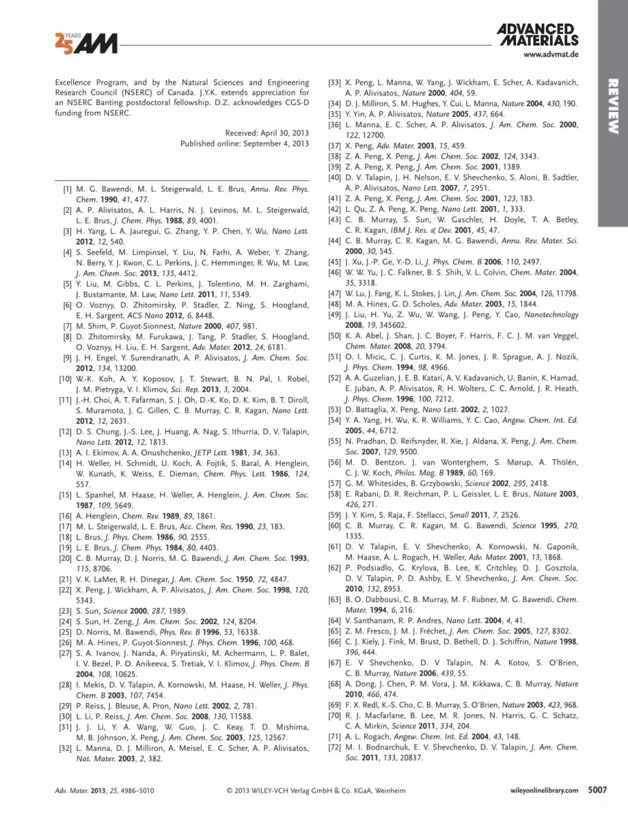
REV
IEW
www.advmat.de
Excellence Program, and by the Natural Sciences and Engineering Research Council (NSERC) of Canada. J.Y.K. extends appreciation for an NSERC Banting postdoctoral fellowship. D.Z. acknowledges CGS-D funding from NSERC.
Received: April 30, 2013 Published online: September 4, 2013
[1] M. G. Bawendi , M. L. Steigerwald , L. E. Brus , Annu. Rev. Phys. Chem. 1990 , 41 , 477 .
[2] A. P. Alivisatos , A. L. Harris , N. J. Levinos , M. L. Steigerwald , L. E. Brus , J. Chem. Phys. 1988 , 89 , 4001 .
[3] H. Yang , L. A. Jauregui , G. Zhang , Y. P. Chen , Y. Wu , Nano Lett. 2012 , 12 , 540 .
[4] S. Seefeld , M. Limpinsel , Y. Liu , N. Farhi , A. Weber , Y. Zhang , N. Berry , Y. J. Kwon , C. L. Perkins , J. C. Hemminger , R. Wu , M. Law , J. Am. Chem. Soc. 2013 , 135 , 4412 .
[5] Y. Liu , M. Gibbs , C. L. Perkins , J. Tolentino , M. H. Zarghami , J. Bustamante , M. Law , Nano Lett. 2011 , 11 , 5349 .
[6] O. Voznyy , D. Zhitomirsky , P. Stadler , Z. Ning , S. Hoogland , E. H. Sargent , ACS Nano 2012 , 6 , 8448 .
[7] M. Shim , P. Guyot-Sionnest , Nature 2000 , 407 , 981 . [8] D. Zhitomirsky , M. Furukawa , J. Tang , P. Stadler , S. Hoogland ,
O. Voznyy , H. Liu , E. H. Sargent , Adv. Mater. 2012 , 24 , 6181 . [9] J. H. Engel , Y. Surendranath , A. P. Alivisatos , J. Am. Chem. Soc.
2012 , 134 , 13200 . [10] W.-K. Koh , A. Y. Koposov , J. T. Stewart , B. N. Pal , I. Robel ,
J. M. Pietryga , V. I. Klimov , Sci. Rep. 2013 , 3 , 2004 . [11] J.-H. Choi , A. T. Fafarman , S. J. Oh , D.-K. Ko , D. K. Kim , B. T. Diroll ,
S. Muramoto , J. G. Gillen , C. B. Murray , C. R. Kagan , Nano Lett. 2012 , 12 , 2631 .
[12] D. S. Chung , J.-S. Lee , J. Huang , A. Nag , S. Ithurria , D. V. Talapin , Nano Lett. 2012 , 12 , 1813 .
[13] A. I. Ekimov , A. A. Onushchenko , JETP Lett. 1981 , 34 , 363 . [14] H. Weller , H. Schmidt , U. Koch , A. Fojtik , S. Baral , A. Henglein ,
W. Kunath , K. Weiss , E. Dieman , Chem. Phys. Lett. 1986 , 124 , 557 .
[15] L. Spanhel , M. Haase , H. Weller , A. Henglein , J. Am. Chem. Soc. 1987 , 109 , 5649 .
[16] A. Henglein , Chem. Rev. 1989 , 89 , 1861 . [17] M. L. Steigerwald , L. E. Brus , Acc. Chem. Res. 1990 , 23 , 183 . [18] L. Brus , J. Phys. Chem. 1986 , 90 , 2555 . [19] L. E. Brus , J. Chem. Phys. 1984 , 80 , 4403 . [20] C. B. Murray , D. J. Norris , M. G. Bawendi , J. Am. Chem. Soc. 1993 ,
115 , 8706 . [21] V. K. LaMer , R. H. Dinegar , J. Am. Chem. Soc. 1950 , 72 , 4847 . [22] X. Peng , J. Wickham , A. P. Alivisatos , J. Am. Chem. Soc. 1998 , 120 ,
5343 . [23] S. Sun , Science 2000 , 287 , 1989 . [24] S. Sun , H. Zeng , J. Am. Chem. Soc. 2002 , 124 , 8204 . [25] D. Norris , M. Bawendi , Phys. Rev. B 1996 , 53 , 16338 . [26] M. A. Hines , P. Guyot-Sionnest , J. Phys. Chem. 1996 , 100 , 468 . [27] S. A. Ivanov , J. Nanda , A. Piryatinski , M. Achermann , L. P. Balet ,
I. V. Bezel , P. O. Anikeeva , S. Tretiak , V. I. Klimov , J. Phys. Chem. B 2004 , 108 , 10625 .
[28] I. Mekis , D. V. Talapin , A. Kornowski , M. Haase , H. Weller , J. Phys. Chem. B 2003 , 107 , 7454 .
[29] P. Reiss , J. Bleuse , A. Pron , Nano Lett. 2002 , 2 , 781 . [30] L. Li , P. Reiss , J. Am. Chem. Soc. 2008 , 130 , 11588 . [31] J. J. Li , Y. A. Wang , W. Guo , J. C. Keay , T. D. Mishima ,
M. B. Johnson , X. Peng , J. Am. Chem. Soc. 2003 , 125 , 12567 . [32] L. Manna , D. J. Milliron , A. Meisel , E. C. Scher , A. P. Alivisatos ,
Nat. Mater. 2003 , 2 , 382 .
© 2013 WILEY-VCH Verlag GAdv. Mater. 2013, 25, 4986–5010
[33] X. Peng , L. Manna , W. Yang , J. Wickham , E. Scher , A. Kadavanich , A. P. Alivisatos , Nature 2000 , 404 , 59 .
[34] D. J. Milliron , S. M. Hughes , Y. Cui , L. Manna , Nature 2004 , 430 , 190 . [35] Y. Yin , A. P. Alivisatos , Nature 2005 , 437 , 664 . [36] L. Manna , E. C. Scher , A. P. Alivisatos , J. Am. Chem. Soc. 2000 ,
122 , 12700 . [37] X. Peng , Adv. Mater. 2003 , 15 , 459 . [38] Z. A. Peng , X. Peng , J. Am. Chem. Soc. 2002 , 124 , 3343 . [39] Z. A. Peng , X. Peng , J. Am. Chem. Soc. 2001 , 1389 . [40] D. V. Talapin , J. H. Nelson , E. V. Shevchenko , S. Aloni , B. Sadtler ,
A. P. Alivisatos , Nano Lett. 2007 , 7 , 2951 . [41] Z. A. Peng , X. Peng , J. Am. Chem. Soc. 2001 , 123 , 183 . [42] L. Qu , Z. A. Peng , X. Peng , Nano Lett. 2001 , 1 , 333 . [43] C. B. Murray , S. Sun , W. Gaschler , H. Doyle , T. A. Betley ,
C. R. Kagan , IBM J. Res. & Dev. 2001 , 45 , 47 . [44] C. B. Murray , C. R. Kagan , M. G. Bawendi , Annu. Rev. Mater. Sci.
2000 , 30 , 545 . [45] J. Xu , J.-P. Ge , Y.-D. Li , J. Phys. Chem. B 2006 , 110 , 2497 . [46] W. W. Yu , J. C. Falkner , B. S. Shih , V. L. Colvin , Chem. Mater. 2004 ,
35 , 3318 . [47] W. Lu , J. Fang , K. L. Stokes , J. Lin , J. Am. Chem. Soc. 2004 , 126 , 11798 . [48] M. A. Hines , G. D. Scholes , Adv. Mater. 2003 , 15 , 1844 . [49] J. Liu , H. Yu , Z. Wu , W. Wang , J. Peng , Y. Cao , Nanotechnology
2008 , 19 , 345602 . [50] K. A. Abel , J. Shan , J. C. Boyer , F. Harris , F. C. J. M. van Veggel ,
Chem. Mater. 2008 , 20 , 3794 . [51] O. I. Micic , C. J. Curtis , K. M. Jones , J. R. Sprague , A. J. Nozik ,
J. Phys. Chem. 1994 , 98 , 4966 . [52] A. A. Guzelian , J. E. B. Katari , A. V. Kadavanich , U. Banin , K. Hamad ,
E. Juban , A. P. Alivisatos , R. H. Wolters , C. C. Arnold , J. R. Heath , J. Phys. Chem. 1996 , 100 , 7212 .
[53] D. Battaglia , X. Peng , Nano Lett. 2002 , 2 , 1027 . [54] Y. A. Yang , H. Wu , K. R. Williams , Y. C. Cao , Angew. Chem. Int. Ed.
2005 , 44 , 6712 . [55] N. Pradhan , D. Reifsnyder , R. Xie , J. Aldana , X. Peng , J. Am. Chem.
Soc. 2007 , 129 , 9500 . [56] M. D. Bentzon , J. van Wonterghem , S. Mørup , A. Thölén ,
C. J. W. Koch , Philos. Mag. B 1989 , 60 , 169 . [57] G. M. Whitesides , B. Grzybowski , Science 2002 , 295 , 2418 . [58] E. Rabani , D. R. Reichman , P. L. Geissler , L. E. Brus , Nature 2003 ,
426 , 271 . [59] J. Y. Kim , S. Raja , F. Stellacci , Small 2011 , 7 , 2526 . [60] C. B. Murray , C. R. Kagan , M. G. Bawendi , Science 1995 , 270 ,
1335 . [61] D. V. Talapin , E. V. Shevchenko , A. Kornowski , N. Gaponik ,
M. Haase , A. L. Rogach , H. Weller , Adv. Mater. 2001 , 13 , 1868 . [62] P. Podsiadlo , G. Krylova , B. Lee , K. Critchley , D. J. Gosztola ,
D. V. Talapin , P. D. Ashby , E. V. Shevchenko , J. Am. Chem. Soc. 2010 , 132 , 8953 .
[63] B. O. Dabbousi , C. B. Murray , M. F. Rubner , M. G. Bawendi , Chem. Mater. 1994 , 6 , 216 .
[64] V. Santhanam , R. P. Andres , Nano Lett. 2004 , 4 , 41 . [65] Z. M. Fresco , J. M. J. Fréchet , J. Am. Chem. Soc. 2005 , 127 , 8302 . [66] C. J. Kiely , J. Fink , M. Brust , D. Bethell , D. J. Schiffrin , Nature 1998 ,
396 , 444 . [67] E. V Shevchenko , D. V Talapin , N. A. Kotov , S. O’Brien ,
C. B. Murray , Nature 2006 , 439 , 55 . [68] A. Dong , J. Chen , P. M. Vora , J. M. Kikkawa , C. B. Murray , Nature
2010 , 466 , 474 . [69] F. X. Redl , K.-S. Cho , C. B. Murray , S. O'Brien , Nature 2003 , 423 , 968 . [70] R. J. Macfarlane , B. Lee , M. R. Jones , N. Harris , G. C. Schatz ,
C. A. Mirkin , Science 2011 , 334 , 204 . [71] A. L. Rogach , Angew. Chem. Int. Ed. 2004 , 43 , 148 . [72] M. I. Bodnarchuk , E. V. Shevchenko , D. V. Talapin , J. Am. Chem.
Soc. 2011 , 133 , 20837 .
5007wileyonlinelibrary.commbH & Co. KGaA, Weinheim

5008
REV
IEW
www.advmat.de
[73] X. Michalet , F. F. Pinaud , L. A. Bentolila , J. M. Tsay , S. Doose , J. J. Li , G. Sundaresan , A. M. Wu , S. S. Gambhir , S. Weiss , Science 2005 , 307 , 538 .
[74] Y. Shirasaki , G. J. Supran , M. G. Bawendi , V. Bulovic , Nat. Photonics 2012 , 7 , 13 .
[75] V. I. Klimov , S. A. Ivanov , J. Nanda , M. Achermann , I. Bezel , J. A. McGuire , A. Piryatinski , Nature 2007 , 447 , 441 .
[76] F. W. Wise , Acc. Chem. Res. 2000 , 33 , 773 . [77] F. Garcia-Santamaria , Y. Chen , J. Vela , R. D. Schaller , J. A. Hollingsworth ,
V. I. Klimov , Nano Lett. 2009 , 9 , 3482 . [78] S. M. Harrell , J. R. McBride , S. J. Rosenthal , Chem. Mater. 2013 ,
25 , 1199 . [79] S. Ithurria , M. D. Tessier , B. Mahler , R. P. S. M. Lobo , B. Dubertret ,
A. L. Efros , Nat. Mater. 2011 , 10 , 936 . [80] D. P. Puzzo , E. J. Henderson , M. G. Helander , Z. Wang ,
G. A. Ozin , Z. Lu , Nano Lett. 2011 , 11 , 1585 . [81] M. Nirmal , D. Norris , M. Kuno , M. G. Bawendi , A. L. Efros ,
M. Rosen , Phys. Rev. Lett. 1995 , 75 , 3728 . [82] M. Kuno , J. K. Lee , B. O. Dabbousi , F. V. Mikulec , M. G. Bawendi ,
J. Chem. Phys. 1997 , 106 . [83] B. L. Wehrenberg , C. Wang , P. Guyot-Sionnest , J. Phys. Chem. B
2002 , 106 , 10634 . [84] A. L. Efros , A. L. Efros , Sov. Phys. Semicond. 1982 , 16 , 772 . [85] L. E. Brus , J. Chem. Phys. 1984 , 79 , 5566 . [86] I. Kang , F. W. Wise , J. Opt. Soc. Am. B 1997 , 14 , 1632 . [87] A. L. Efros , M. Rosen , M. Kuno , M. Nirmal , D. J. Norris ,
M. G. Bawendi , Phys. Rev. B 1996 , 54 , 4843 . [88] G. Bester , J. Phys.: Condens. Matter 2009 , 21 , 023202 . [89] G. Allan , C. Delerue , Phys. Rev. B 2004 , 70 , 245321 . [90] M. Korkusinski , O. Voznyy , P. Hawrylak , Phys. Rev. B 2010 , 82 ,
245304 . [91] A. Franceschetti , J. M. An , A. Zunger , Nano Lett. 2007 , 7 , 2129 . [92] J. Kim , C. Y. Wong , G. Scholes , Acc. Chem. Res. 2009 , 42 , 1037 . [93] H. Zhong , G. Scholes , M. Nagy , M. Jones , J. Phys. Chem. C 2009 ,
113 , 10465 . [94] M. Jones , S. S. Lo , G. Scholes , Proc. Natl. Acad. Sci. 2009 , 106 , 3011 . [95] C. de Mello Donegá , M. Bode , A. Meijerink , Phys. Rev. B 2006 , 74 ,
085320 . [96] O. Voznyy , J. Phys. Chem. C 2011 , 115 , 15927 . [97] A. L. Rogach , T. Franzl , T. A. Klar , J. Feldmann , N. Gaponik ,
V. Lesnyak , A. Shavel , A. Eychmuller , Y. P. Rakovich , J. F. Donegan , J. Phys. Chem. C 2007 , 111 , 14628 .
[98] A. M. Smith , S. Nie , Acc. Chem. Res. 2010 , 43 , 190 . [99] H. H.-Y. Wei , C. M. Evans , B. D. Swartz , A. J. Neukirch , J. Young ,
O. V Prezhdo , T. D. Krauss , Nano Lett. 2012 , 12 , 4465 . [100] M. Nirmal , B. O. Dabbousi , M. G. Bawendi , J. J. Macklin ,
J. K. Trautman , T. D. Harris , L. E. Brus , Nature 1996 , 383 , 802 . [101] D. I. Chepic , A. I. Ekimov , M. G. Ivanov , V. A. Kharchenko ,
T. V. Yazeva , J. Luminescence 1990 , 47 , 113 . [102] P. Frantsuzov , M. Kuno , B. Jankó , R. A. Marcus , Nat. Phys. 2008 , 4 ,
519 . [103] F. M. Gómez-Campos , M. Califano , Nano Lett. 2012 , 12 , 4508 . [104] S. A. Empedocles , M. G. Bawendi , Science 1997 , 278 , 2114 . [105] R. G. Neuhauser , K. T. Shimizu , W. K. Woo , S. A. Empedocles ,
M. G. Bawendi , Phys. Rev. Lett. 2000 , 85 , 3301 . [106] P. P. Jha , P. Guyot-Sionnest , ACS Nano 2009 , 3 , 1011 . [107] S. Rosen , O. Schwartz , D. Oron , Phys. Rev. Lett. 2010 , 104 , 157404 . [108] J. Zhao , G. Nair , B. R. Fisher , M. G. Bawendi , Phys. Rev. Lett. 2010 ,
104 , 157403 . [109] P. Frantsuzov , S. Volkan-Kacso , B. Janko , Nano Lett. 2013 , 13 , 402 . [110] C. Galland , Y. Ghosh , A. Steinbrück , M. Sykora , J. A. Hollingsworth ,
V. I. Klimov , H. Htoon , Nature 2011 , 479 , 203 . [111] A. A. Cordones , S. R. Leone , Chem. Soc. Rev. 2013 , 42 , 3209 . [112] O. Voznyy , S. M. Thon , A. H. Ip , E. H. Sargent , J. Phys. Chem. Lett.
2013 , 4 , 987 .
wileyonlinelibrary.com © 2013 WILEY-VCH Verlag
[113] B. Mahler , P. Spinicelli , S. Buil , X. Quelin , J.-P. Hermier , B. Dubertret , Nat. Mater. 2008 , 7 , 659 .
[114] Y. Chen , J. Vela , H. Htoon , J. L. Casson , D. J. Werder , D. A. Bussian , V. I. Klimov , J. A. Hollingsworth , J. Am. Chem. Soc. 2008 , 130 , 5026 .
[115] X. Wang , X. Ren , K. Kahen , M. A. Hahn , M. Rajeswaran , S. Maccagnano-Zacher , J. Silcox , G. E. Cragg , A. L. Efros , T. D. Krauss , Nature 2009 , 459 , 686 .
[116] O. Chen , J. Zhao , V. P. Chauhan , J. Cui , C. Wong , D. K. Harris , H. Wei , H.-S. Han , D. Fukumura , R. K. Jain , M. G. Bawendi , Nat. Mater. 2013 , 12 , 1 .
[117] M. D. Pashley , Phys. Rev. B 1989 , 40 , 10481 . [118] A. Puzder , A. J. Williamson , F. Gygi , G. Galli , Phys. Rev. Lett. 2004 ,
92 , 217401 . [119] A. J. Nozik , Chem. Phys. Lett. 2008 , 457 , 3 . [120] A. J. Nozik , Physica E 2002 , 14 , 115 . [121] R. D. Schaller , V. I. Klimov , Phys. Rev. Lett. 2004 , 92 , 186601 . [122] R. D. Schaller , M. Sykora , J. M. Pietryga , V. I. Klimov , Nano Lett.
2006 , 6 , 424 . [123] R. R. Cooney , S. L. Sewall , E. A. Dias , K. E. H. Anderson ,
P. Kambhampati , Phys. Rev. Lett. 2007 , 98 , 1 . [124] O. V. Prezhdo , Acc. Chem. Res. 2009 , 42 , 2005 . [125] A. Pandey , P. Guyot-Sionnest , Science 2008 , 322 , 929 . [126] M. C. Beard , R. J. Ellingson , Laser Photon. Rev. 2008 , 2 , 377 . [127] V. I. Klimov , J. A. McGuire , R. D. Schaller , V. I. Rupasov , Phys. Rev.
B 2008 , 77 , 195324 . [128] R. D. Schaller , J. M. Pietryga , V. I. Klimov , Nano Lett. 2007 , 7 , 3469 . [129] G. Nair , L.-Y. Chang , S. M. Geyer , M. G. Bawendi , Nano Lett. 2011 ,
11 , 2145 . [130] J. A. McGuire , M. Sykora , I. Robel , L. A. Padilha , J. Joo ,
J. M. Pietryga , V. I. Klimov , ACS Nano 2010 , 4 , 6087 . [131] P. Tyagi , P. Kambhampati , J. Chem. Phys. 2011 , 134 , 094706 . [132] P. Kambhampati , Acc. Chem. Res. 2011 , 44 , 1 . [133] M. T. Trinh , A. J. Houtepen , J. M. Schins , T. Hanrath , J. Piris ,
W. Knulst , A. P. L. M. Goossens , L. D. A. Siebbeles , Nano Lett. 2008 , 8 , 1713 .
[134] J. A. McGuire , M. Sykora , J. Joo , J. M. Pietryga , V. I. Klimov , Nano Lett. 2010 , 10 , 2049 .
[135] L. A. Padilha , J. T. Stewart , R. L. Sandberg , W. K. Bae , W.-K. Koh , J. M. Pietryga , V. I. Klimov , Acc. Chem. Res. 2013 , 46 , 1261 .
[136] V. Sukhovatkin , S. Hinds , L. Brzozowski , E. H. Sargent , Science 2009 , 324 , 1542 .
[137] O. E. Semonin , J. M. Luther , S. Choi , H.-Y. Chen , J. Gao , A. J. Nozik , M. C. Beard , Science (New York, NY) 2011 , 334 , 1530 .
[138] A. Shabaev , C. S. Hellberg , A. L. Efros , Acc. Chem. Res. 2013 , 46 , 1242 . [139] V. Rupasov , V. I. Klimov , Phys. Rev. B 2007 , 76 , 125321 . [140] A. Franceschetti , J. M. An , A. Zunger , Nano Lett. 2006 , 6 , 2191 . [141] J. J. H. Pijpers , R. Ulbricht , K. J. Tielrooij , A. Osherov , Y. Golan ,
C. Delerue , G. Allan , M. Bonn , Nat. Phys. 2009 , 5 , 811 . [142] A. Bartnik , A. Efros , W.-K. Koh , C. Murray , F. Wise , Phys. Rev. B
2010 , 82 , 195313 . [143] D. L. Klein , R. Roth , A. K. L. Lim , A. P. Alivisatos , P. L. McEuen ,
Nature 1997 , 323 , 699 . [144] D. Katz , T. Wizansky , O. Millo , E. Rothenberg , T. Mokari , U. Banin ,
Phys. Rev. Lett. 2002 , 89 , 086801 . [145] U. Banin , Y. Cao , D. Katz , O. Millo , Nature 1999 , 400 , 542 . [146] G. Medeiros-Ribeiro , D. Ohlberg , R. Williams , J. Heath , Phys. Rev.
B 1999 , 59 , 1633 . [147] A. Zabet-Khosousi , A.-A. Dhirani , Chem. Rev. 2008 , 108 , 4072 . [148] D. S. Ginger , N. C. Greenham , J. Appl. Phys. 2000 , 87 , 1361 . [149] N. Morgan , C. Leatherdale , M. Drndic , M. Jarosz , M. Kastner ,
M. Bawendi , Phys. Rev. B 2002 , 66 , 075339 . [150] D. Novikov , M. Drndic , L. Levitov , M. Kastner , M. Jarosz ,
M. Bawendi , Phys. Rev. B 2005 , 72 , 075309 . [151] C. Leatherdale , C. Kagan , N. Morgan , S. Empedocles , M. Kastner ,
M. Bawendi , Phys. Rev. B 2000 , 62 , 2669 .
GmbH & Co. KGaA, Weinheim Adv. Mater. 2013, 25, 4986–5010

REV
IEW
www.advmat.de
[152] L. Turyanska , U. Elfurawi , M. Li , M. W. Fay , N. R. Thomas , S. Mann , J. H. Blokland , P. C. M. Christianen , A. Patanè , Nanotechnology 2009 , 20 , 315604 .
[153] M. Drndic , M. V. Jarosz , N. Y. Morgan , M. A. Kastner , M. G. Bawendi , J. Appl. Phys. 2002 , 92 , 7498 .
[154] P. Guyot-Sionnest , C. Wang , J. Phys. Chem. B 2003 , 107 , 7355 . [155] M. Jarosz , V. Porter , B. Fisher , M. Kastner , M. Bawendi , Phys. Rev. B
2004 , 70 , 195327 . [156] D. V. Talapin , C. B. Murray , Science 2005 , 310 , 86 . [157] D. Yu , C. Wang , P. Guyot-Sionnest , Science 2003 , 300 , 1277 . [158] C. Wang , M. Shim , P. Guyot-Sionnest , Science 2001 , 291 , 2390 . [159] C. Wang , M. Shim , P. Guyot-Sionnest , Appl. Phys. Lett. 2002 , 80 , 4 . [160] D. Vanmaekelbergh , P. Liljeroth , Chem. Soc. Rev. 2005 , 34 , 299 . [161] E. Talgorn , Y. Gao , M. Aerts , L. T. Kunneman , J. M. Schins ,
T. J. Savenije , M. A. van Huis , H. S. J. van der Zant , A. J. Houtepen , L. D. A. Siebbeles , Nat. Nanotechnol. 2011 , 6 , 733 .
[162] D. V. Talapin , J.-S. Lee , M. V. Kovalenko , E. V. Shevchenko , Chem. Rev. 2010 , 110 , 389 .
[163] H. Liu , A. Pourret , P. Guyot-Sionnest , ACS Nano 2010 , 4 , 5211 . [164] Y. Liu , M. Gibbs , J. Puthussery , S. Gaik , R. Ihly , H. W. Hillhouse ,
M. Law , Nano Lett. 2010 , 10 , 1960 . [165] I. Chu , M. Radulaski , N. Vukmirovic , H. Cheng , L. Wang , J. Phys.
Chem. C 2011 , 115 , 21409 . [166] P. Guyot-Sionnest , J. Phys. Chem. Lett. 2012 , 3 , 1169 . [167] F. Remacle , R. D. Levine , Chem. Phys. Chem. 2001 , 2 , 20 . [168] I. Beloborodov , A. Lopatin , V. Vinokur , K. Efetov , Rev. Mod. Phys.
2007 , 79 , 469 . [169] P. Nagpal , V. I. Klimov , Nat. Commun. 2011 , 2 , 486 . [170] M. V. Kovalenko , D. V. Talapin , M. Scheele , Science 2009 , 324 , 1417 . [171] Y. Gao , M. Aerts , C. S. Suchand Sandeep , E. Talgorn , T. J. Savenije ,
S. Kinge , L. D. A. Siebbeles , A. J. Houtepen , ACS Nano 2012 , 6 , 9606 . [172] B.-R. Hyun , A. C. Bartnik , L. Sun , T. Hanrath , F. W. Wise , Nano
Lett. 2011 , 11 , 2126 . [173] A. Wolcott , V. Doyeux , J. Phys. Chem. Lett. 2011 , 2 , 795 . [174] A. H. Ip , S. M. Thon , S. Hoogland , O. Voznyy , D. Zhitomirsky ,
R. Debnath , L. Levina , L. R. Rollny , G. H. Carey , A. Fischer , K. W. Kemp , I. J. Kramer , Z. Ning , A. J. Labelle , K. W. Chou , A. Amassian , E. H. Sargent , Nat. Nanotechnol. 2012 , 7 , 577 .
[175] E. Kinder , P. Moroz , G. Diederich , A. Johnson , M. Kirsanova , A. Nemchinov , T. O’Connor , D. Roth , M. Zamkov , J. Am. Chem. Soc. 2011 , 133 , 20488 .
[176] Y. Liu , J. Tolentino , M. Gibbs , R. Ihly , C. L. Perkins , Y. Liu , N. Crawford , J. C. Hemminger , M. Law , Nano Lett. 2013 , 13 , 1578 .
[177] I. Gur , N. A. Fromer , M. L. Geier , A. P. Alivisatos , Science 2005 , 310 , 462 .
[178] B. I. Macdonald , A. Martucci , S. Rubanov , S. E. Watkins , P. Mulvaney , J. J. Jasieniak , ACS Nano 2012 , 6 , 5995 .
[179] M. Green , J. Mater. Chem. 2010 , 20 , 5797 . [180] S. V. Voitekhovich , D. V. Talapin , Chem. Mater. 2008 , 20 , 4545 . [181] J. S. Owen , J. Park , P.-E. Trudeau , A. P. Alivisatos , J. Am. Chem.
Soc. 2008 , 130 , 12279 . [182] N. C. Anderson , J. S. Owen , Chem. Mater. 2013 , 25 , 69 . [183] X. Wang , G. I. Koleilat , J. Tang , H. Liu , I. J. Kramer , R. Debnath ,
L. Brzozowski , D. A. R. Barkhouse , L. Levina , S. Hoogland , E. H. Sargent , Nat. Photonics 2011 , 5 , 480 .
[184] J. M. Caruge , J. E. Halpert , V. Wood , V. Bulovic , M. G. Bawendi , Nat. Photonics 2008 , 2 , 247 .
[185] M. V. Kovalenko , B. Spokoyny , J.-S. Lee , M. Scheele , A. Weber , S. Perera , D. Landry , D. V. Talapin , J. Am. Chem. Soc. 2010 , 132 , 6686 .
[186] I. J. Kramer , E. H. Sargent , ACS Nano 2011 , 5 , 8506 . [187] E. H. Sargent , Nat. Photonics 2012 , 6 , 133 . [188] S. A. McDonald , G. Konstantatos , S. Zhang , P. W. Cyr ,
E. J. D. Klem , L. Levina , E. H. Sargent , Nat. Mater. 2005 , 4 , 138 .
© 2013 WILEY-VCH Verlag GmAdv. Mater. 2013, 25, 4986–5010
[189] A. Maria , P. W. Cyr , E. J. D. Klem , L. Levina , E. H. Sargent , Appl. Phys. Lett. 2005 , 87 , 213112 .
[190] J. Tang , X. Wang , L. Brzozowski , D. A. R. Barkhouse , R. Debnath , L. Levina , E. H. Sargent , Adv. Mater. 2010 , 22 , 1398 .
[191] G. Konstantatos , I. Howard , A. Fischer , S. Hoogland , J. Clifford , E. Klem , L. Levina , E. H. Sargent , Nature 2006 , 442 , 180 .
[192] J.-S. Lee , E. V. Shevchenko , D. V. Talapin , J. Am. Chem. Soc. 2008 , 130 , 9673 .
[193] M. Soreni-Harari , N. Yaacobi-Gross , D. Steiner , A. Aharoni , U. Banin , O. Millo , N. Tessler , Nano Lett. 2008 , 8 , 678 .
[194] J. M. Luther , J. Gao , M. T. Lloyd , O. E. Semonin , M. C. Beard , A. J. Nozik , Adv. Mater. 2010 , 22 , 3704 .
[195] A. G. Pattantyus-Abraham , I. J. Kramer , A. R. Barkhouse , X. Wang , G. Konstantatos , R. Debnath , L. Levina , I. Raabe , M. K. Nazeeruddin , M. Grätzel , E. H. Sargent , ACS Nano 2010 , 4 , 3374 .
[196] H. Liu , J. Tang , I. J. Kramer , R. Debnath , G. I. Koleilat , X. Wang , A. Fisher , R. Li , L. Brzozowski , L. Levina , E. H. Sargent , Adv. Mater. 2011 , 23 , 3832 .
[197] J. Tang , K. W. Kemp , S. Hoogland , K. S. Jeong , H. Liu , L. Levina , M. Furukawa , X. Wang , R. Debnath , D. Cha , K. W. Chou , A. Fischer , A. Amassian , J. B. Asbury , E. H. Sargent , Nat. Mater. 2011 , 10 , 765 .
[198] I. J. Kramer , D. Zhitomirsky , J. D. Bass , P. M. Rice , T. Topuria , L. Krupp , S. M. Thon , A. H. Ip , R. Debnath , H.-C. Kim , E. H. Sargent , Adv. Mater. 2012 , 24 , 2315 .
[199] X. Lan , J. Bai , S. Masala , S. M. Thon , Y. Ren , I. J. Kramer , S. Hoogland , A. Simchi , G. I. Koleilat , D. Paz-Soldan , Z. Ning , A. J. Labelle , J. Y. Kim , G. Jabbour , E. H. Sargent , Adv. Mater. 2013 , 25 , 1769 .
[200] H. Lee , H. C. Leventis , S.-J. Moon , P. Chen , S. Ito , S. A. Haque , T. Torres , F. Nüesch , T. Geiger , S. M. Zakeeruddin , M. Grätzel , M. K. Nazeeruddin , Adv. Funct. Mater. 2009 , 19 , 2735 .
[201] O. von Roos , J. Appl. Phys. 1978 , 49 , 3503 . [202] M. Wolf , Proc. IEEE 1963 , 51 , 674 . [203] P. Peumans , S. R. Forrest , Appl. Phys. Lett. 2001 , 79 , 126 . [204] C. J. Brabec , S. E. Shaheen , C. Winder , N. S. Sariciftci , P. Denk ,
Appl. Phys. Lett. 2002 , 80 , 1288 . [205] B. E. Hardin , E. T. Hoke , P. B. Armstrong , J.-H. Yum ,
P. Comte , T. Torres , J. M. J. Fréchet , M. K. Nazeeruddin , M. Grätzel , M. D. McGehee , Nat. Photonics 2009 , 3 , 406 .
[206] S. Guha , J. Yang , A. Pawlikiewicz , T. Glatfelter , R. Ross , S. R. Ovshinsky , Appl. Phys. Lett. 1989 , 54 , 2330 .
[207] I. J. Kramer , L. Levina , R. Debnath , D. Zhitomirsky , E. H. Sargent , Nano Lett. 2011 , 11 , 3701 .
[208] D. Zhitomirsky , I. J. Kramer , A. J. Labelle , A. Fischer , R. Debnath , J. Pan , O. M. Bakr , E. H. Sargent , Nano Lett. 2012 , 12 , 1007 .
[209] A. Sahu , M. S. Kang , A. Kompch , C. Notthoff , A. W. Wills , D. Deng , M. Winterer , C. D. Frisbie , D. J. Norris , Nano Lett. 2012 , 12 , 2587 .
[210] D. J. Norris , A. L. Efros , S. C. Erwin , Science 2008 , 319 , 1776 . [211] S. M. Geyer , P. M. Allen , L.-Y. Chang , C. R. Wong , T. P. Osedach ,
N. Zhao , V. Bulovic , M. G. Bawendi , ACS Nano 2010 , 4 , 7373 . [212] D. Mocatta , G. Cohen , J. Schattner , O. Millo , E. Rabani , U. Banin ,
Science 2011 , 332 , 77 . [213] H. Liu , S. Keuleyan , P. Guyot-Sionnest , J. Phys. Chem. C 2012 , 116 ,
1344 . [214] J. Tang , H. Liu , D. Zhitomirsky , S. Hoogland , X. Wang , M. Furukawa ,
L. Levina , E. H. Sargent , Nano Lett. 2012 , 12 , 4889 . [215] Z. Ning , D. Zhitomirsky , V. Adinolfi , B. Sutherland , J. Xu ,
O. Voznyy , P. Maraghechi , X. Lan , S. Hoogland , Y. Ren , E. H. Sargent , Adv. Mater. 2013 , 25 , 1719 .
[216] J.-S. Lee , M. V. Kovalenko , J. Huang , D. S. Chung , D. V. Talapin , Nat. Nanotechnol. 2011 , 6 , 348 .
5009wileyonlinelibrary.combH & Co. KGaA, Weinheim

Opt In for
until Jan 2015Free Access
Editorial Advisory Board
Hatice AltugRichard AverittPaul BraunMark BrongersmaTimothy J. BunningCornelia DenzHarald GiessenPeter GünterZhi-Yuan LiDavid LidzeyLuis Liz-MarzánCefe LópezStefan MaierHolger MoenchDan OronAlbert PolmanUllrich SteinerJianfang WangRalf WehrspohnMartin Wegener
Advanced Optical Materials is an international, interdisciplinary forum for peer-reviewed papers dedicated to breakthrough discoveries and fun-damental research in the fi eld of optical mate-rials. The scope of the journal covers all aspects of light-matter interactions including metama-terials and plasmonics, optical nanostructures, optical devices, photonics and more.
Volume 1, 12 issues in 2013. Online ISSN: 2195-1071
Cover picture by Byeong-Kwon Ju, Kyung Cheol Choi and co-workersDOI: 10.1002/adom.201200021
Examples of excellent papers published in Advanced Optical Materials:
Magnetoplasmonics: Combining Magnetic and Plasmonic FunctionalitiesGaspar Armelles, Alfonso Cebollada*, Antonio García-Martín, María Ujué González
http://onlinelibrary.wiley.com/doi/10.1002/adom.201200011/full
Optically Reconfi gurable Refl ective/Scattering States Enabled with Photosensitive Cholesteric Liquid Crystal CellsJ. P. Vernon, U. A. Hrozhyk, S. V. Serak, V. P. Tondiglia, T. J. White, N. V. Tabiryan, T. J. Bunning
http://onlinelibrary.wiley.com/doi/10.1002/adom.201200014/full
Fast and Low-Power All-Optical Tunable Fano Resonance in Plasmonic MicrostructuresY. Zhu, X. Hu, Y. Huang, H.Yang, Q. Gong
http://onlinelibrary.wiley.com/doi/10.1002/adom.201200025/full
ZnO p–n Homojunction Random Laser Diode Based on Nitrogen-Doped p-type NanowiresJ. Huang, S. Chu, J. Kong, L. Zhang, C. M. Schwarz, G. Wang, L. Chernyak, Z. Chen, J. Liu
http://onlinelibrary.wiley.com/doi/10.1002/adom.201200062/full
Broadband and Effi cient DiffractionC. Ribot, M.-S. Laure Lee, S. Collin, S. Bansropun, P. Plouhinec, D. Thenot, S. Cassette, B. Loiseaux, P. Lalanne
http://onlinelibrary.wiley.com/doi/10.1002/adom.201300215/full
Spoof Plasmon Surfaces: A Novel Platform for THz SensingBinghao Ng, Jianfeng Wu, Stephen M. Hanham, Antonio I. Fernández-Domínguez, Norbert Klein, Yun Fook Liew, Mark B. H. Breese, Minghui Hong, Stefan A. Maier*
http://onlinelibrary.wiley.com/doi/10.1002/adom.201300146/full