1998 core solutions databook (3/2/98) vs 1.0
TRANSCRIPT
R
Section Titles
1. Introduction
2. LogiCORE Products
3. AllianceCORE Products
4. LogiBLOX
5. Reference Designs


R
Table of Contents
IntroductionIntroduction Table of Contents . . . . . . . . . . . . . . . . . . . . . . . . . . . . . . . . . . . . . . . . . .1-2
CORE Solutions Overview . . . . . . . . . . . . . . . . . . . . . . . . . . . . . . . . . . . . . . . . . . . .1-3The Effect of PLD Architecture on Cores . . . . . . . . . . . . . . . . . . . . . . . . . . . . . . . . .1-5XC4000-Series FPGAs: The Best Choice for Delivering Cores . . . . . . . . . . . . . . . .1-9Product Listing by Application Segment . . . . . . . . . . . . . . . . . . . . . . . . . . . . . . . . .1-13
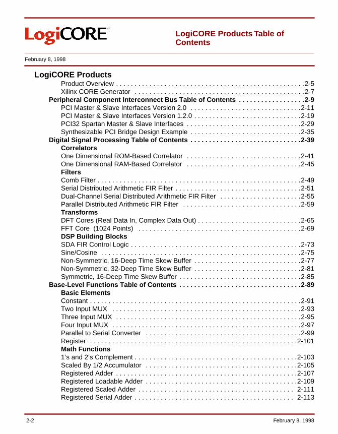
LogiCORE ProductsLogiCORE Products Table of Contents . . . . . . . . . . . . . . . . . . . . . . . . . . . . . . . . . . .2-2
Product Overview . . . . . . . . . . . . . . . . . . . . . . . . . . . . . . . . . . . . . . . . . . . . . . . . . . .2-5Xilinx CORE Generator . . . . . . . . . . . . . . . . . . . . . . . . . . . . . . . . . . . . . . . . . . . . . .2-7
Peripheral Component Interconnect Bus Table of Contents . . . . . . . . . . . . . . . . . .2-9PCI Master & Slave Interfaces Version 2.0 . . . . . . . . . . . . . . . . . . . . . . . . . . . . . .2-11PCI Master & Slave Interfaces Version 1.2.0 . . . . . . . . . . . . . . . . . . . . . . . . . . . . .2-19PCI32 Spartan Master & Slave Interfaces . . . . . . . . . . . . . . . . . . . . . . . . . . . . . . .2-29Synthesizable PCI Bridge Design Example . . . . . . . . . . . . . . . . . . . . . . . . . . . . . .2-35
Digital Signal Processing Table of Contents . . . . . . . . . . . . . . . . . . . . . . . . . . . . . .2-39CorrelatorsOne Dimensional ROM-Based Correlator . . . . . . . . . . . . . . . . . . . . . . . . . . . . . . .2-41One Dimensional RAM-Based Correlator . . . . . . . . . . . . . . . . . . . . . . . . . . . . . . .2-45FiltersComb Filter . . . . . . . . . . . . . . . . . . . . . . . . . . . . . . . . . . . . . . . . . . . . . . . . . . . . . . .2-49Serial Distributed Arithmetic FIR Filter . . . . . . . . . . . . . . . . . . . . . . . . . . . . . . . . . .2-51Dual-Channel Serial Distributed Arithmetic FIR Filter . . . . . . . . . . . . . . . . . . . . . .2-55Parallel Distributed Arithmetic FIR Filter . . . . . . . . . . . . . . . . . . . . . . . . . . . . . . . .2-59TransformsDFT Cores (Real Data In, Complex Data Out) . . . . . . . . . . . . . . . . . . . . . . . . . . . .2-65FFT Core (1024 Points) . . . . . . . . . . . . . . . . . . . . . . . . . . . . . . . . . . . . . . . . . . . .2-69DSP Building BlocksSDA FIR Control Logic . . . . . . . . . . . . . . . . . . . . . . . . . . . . . . . . . . . . . . . . . . . . . .2-73Sine/Cosine . . . . . . . . . . . . . . . . . . . . . . . . . . . . . . . . . . . . . . . . . . . . . . . . . . . . . .2-75Non-Symmetric, 16-Deep Time Skew Buffer . . . . . . . . . . . . . . . . . . . . . . . . . . . . .2-77Non-Symmetric, 32-Deep Time Skew Buffer . . . . . . . . . . . . . . . . . . . . . . . . . . . . .2-81Symmetric, 16-Deep Time Skew Buffer . . . . . . . . . . . . . . . . . . . . . . . . . . . . . . . . .2-85
Base-Level Functions Table of Contents . . . . . . . . . . . . . . . . . . . . . . . . . . . . . . . . .2-89Basic ElementsConstant . . . . . . . . . . . . . . . . . . . . . . . . . . . . . . . . . . . . . . . . . . . . . . . . . . . . . . . . .2-91Two Input MUX . . . . . . . . . . . . . . . . . . . . . . . . . . . . . . . . . . . . . . . . . . . . . . . . . . .2-93Three Input MUX . . . . . . . . . . . . . . . . . . . . . . . . . . . . . . . . . . . . . . . . . . . . . . . . . .2-95Four Input MUX . . . . . . . . . . . . . . . . . . . . . . . . . . . . . . . . . . . . . . . . . . . . . . . . . . .2-97Parallel to Serial Converter . . . . . . . . . . . . . . . . . . . . . . . . . . . . . . . . . . . . . . . . . .2-99
Table of Contents
Register . . . . . . . . . . . . . . . . . . . . . . . . . . . . . . . . . . . . . . . . . . . . . . . . . . . . . . . .2-101Math Functions1’s and 2’s Complement . . . . . . . . . . . . . . . . . . . . . . . . . . . . . . . . . . . . . . . . . . . .2-103Scaled By 1/2 Accumulator . . . . . . . . . . . . . . . . . . . . . . . . . . . . . . . . . . . . . . . . .2-105Registered Adder . . . . . . . . . . . . . . . . . . . . . . . . . . . . . . . . . . . . . . . . . . . . . . . . .2-107Registered Loadable Adder . . . . . . . . . . . . . . . . . . . . . . . . . . . . . . . . . . . . . . . . .2-109Registered Scaled Adder . . . . . . . . . . . . . . . . . . . . . . . . . . . . . . . . . . . . . . . . . . 2-111Registered Serial Adder . . . . . . . . . . . . . . . . . . . . . . . . . . . . . . . . . . . . . . . . . . . 2-113Integrator . . . . . . . . . . . . . . . . . . . . . . . . . . . . . . . . . . . . . . . . . . . . . . . . . . . . . . .2-115Constant Coefficient Multiplier . . . . . . . . . . . . . . . . . . . . . . . . . . . . . . . . . . . . . . .2-117Constant Coefficient Multiplier (Pipelined) . . . . . . . . . . . . . . . . . . . . . . . . . . . . . 2-119Parallel Multipliers - Area Optimized. . . . . . . . . . . . . . . . . . . . . . . . . . . . . . . . . . 2-121Parallel Multipliers - Performance Optimized . . . . . . . . . . . . . . . . . . . . . . . . . . . 2-125Square Root . . . . . . . . . . . . . . . . . . . . . . . . . . . . . . . . . . . . . . . . . . . . . . . . . . . . .2-127Registered Subtracter . . . . . . . . . . . . . . . . . . . . . . . . . . . . . . . . . . . . . . . . . . . . . 2-129Registered Loadable Subtracter . . . . . . . . . . . . . . . . . . . . . . . . . . . . . . . . . . . . . 2-131MemoriesDelay Element . . . . . . . . . . . . . . . . . . . . . . . . . . . . . . . . . . . . . . . . . . . . . . . . . . .2-133Synchronous FIFO . . . . . . . . . . . . . . . . . . . . . . . . . . . . . . . . . . . . . . . . . . . . . . . .2-13516-Word Deep Registered Look-Up Table . . . . . . . . . . . . . . . . . . . . . . . . . . . . . 2-13932-Word Deep Registered Look-Up Table . . . . . . . . . . . . . . . . . . . . . . . . . . . . . 2-141Registered Synchronous RAM . . . . . . . . . . . . . . . . . . . . . . . . . . . . . . . . . . . . . . 2-143Registered ROM . . . . . . . . . . . . . . . . . . . . . . . . . . . . . . . . . . . . . . . . . . . . . . . . .2-145
AllianceCORE ProductsAllianceCORE Products Table of Contents . . . . . . . . . . . . . . . . . . . . . . . . . . . . . . . .3-2
AllianceCORE Program Overview . . . . . . . . . . . . . . . . . . . . . . . . . . . . . . . . . . . . . .3-5Standard Bus Interface Products Table of Contents . . . . . . . . . . . . . . . . . . . . . . . .3-7
XF-TWSI Two-Wire Serial Interface . . . . . . . . . . . . . . . . . . . . . . . . . . . . . . . . . . . . .3-9PCMCIA Fax/Modem Macro . . . . . . . . . . . . . . . . . . . . . . . . . . . . . . . . . . . . . . . . .3-15PCMCIA Library R1.2 . . . . . . . . . . . . . . . . . . . . . . . . . . . . . . . . . . . . . . . . . . . . . . .3-19PCMCIA Prototyping Card . . . . . . . . . . . . . . . . . . . . . . . . . . . . . . . . . . . . . . . . . . .3-23PCMCIA Card Debugger/Exerciser . . . . . . . . . . . . . . . . . . . . . . . . . . . . . . . . . . . .3-25PCMCIA CIS Generator 1.2 . . . . . . . . . . . . . . . . . . . . . . . . . . . . . . . . . . . . . . . . . .3-27Low-Speed USB Function Controller . . . . . . . . . . . . . . . . . . . . . . . . . . . . . . . . . . .3-29Full-Speed USB Function Controller . . . . . . . . . . . . . . . . . . . . . . . . . . . . . . . . . . .3-333-Port USB Hub Controller . . . . . . . . . . . . . . . . . . . . . . . . . . . . . . . . . . . . . . . . . . .3-37USB Function Evaluation Board . . . . . . . . . . . . . . . . . . . . . . . . . . . . . . . . . . . . . . .3-41USB Hub Evaluation Board . . . . . . . . . . . . . . . . . . . . . . . . . . . . . . . . . . . . . . . . . .3-43USB Simulation Model . . . . . . . . . . . . . . . . . . . . . . . . . . . . . . . . . . . . . . . . . . . . . .3-45
Communications and Networking Products Table of Contents . . . . . . . . . . . . . .3-47Cell Assembler (CC-201) . . . . . . . . . . . . . . . . . . . . . . . . . . . . . . . . . . . . . . . . . . . .3-49Cell Delineation (CC-200) . . . . . . . . . . . . . . . . . . . . . . . . . . . . . . . . . . . . . . . . . . .3-53CRC10 Generator and Verifier (CC-130) . . . . . . . . . . . . . . . . . . . . . . . . . . . . . . . .3-57CRC32 Generator and Verifier (CC-131) . . . . . . . . . . . . . . . . . . . . . . . . . . . . . . . .3-61HDLC Protocol Core . . . . . . . . . . . . . . . . . . . . . . . . . . . . . . . . . . . . . . . . . . . . . . .3-65

Reed-Solomon Decoder . . . . . . . . . . . . . . . . . . . . . . . . . . . . . . . . . . . . . . . . . . . . 3-71Reed-Solomon Encoder . . . . . . . . . . . . . . . . . . . . . . . . . . . . . . . . . . . . . . . . . . . . 3-77MT1F T1 Framer . . . . . . . . . . . . . . . . . . . . . . . . . . . . . . . . . . . . . . . . . . . . . . . . . .3-81UTOPIA Slave (CC-141) . . . . . . . . . . . . . . . . . . . . . . . . . . . . . . . . . . . . . . . . . . . .3-85Viterbi Decoder . . . . . . . . . . . . . . . . . . . . . . . . . . . . . . . . . . . . . . . . . . . . . . . . . . .3-91
Processor Products Table of Contents . . . . . . . . . . . . . . . . . . . . . . . . . . . . . . . . . .3-95TX400 Series RISC CPU Cores . . . . . . . . . . . . . . . . . . . . . . . . . . . . . . . . . . . . . . .3-97RISC CPU Core Design Base Board . . . . . . . . . . . . . . . . . . . . . . . . . . . . . . . . . .3-103Scalable Development Platform Integrated Software . . . . . . . . . . . . . . . . . . . . .3-107V8-uRISC 8-bit RISC Microprocessor . . . . . . . . . . . . . . . . . . . . . . . . . . . . . . . . .3-109IntelliCoreTM Prototyping System . . . . . . . . . . . . . . . . . . . . . . . . . . . . . . . . . . . . . 3-115
Processor Peripherals Table of Contents . . . . . . . . . . . . . . . . . . . . . . . . . . . . . . .3-119M16450 Universal Asynchronous Receiver/Transmitter . . . . . . . . . . . . . . . . . . .3-121M16550A - Universal Asynchronous Receiver/Transmitter With FIFOs . . . . . . . .3-125C2910A Microprogram Controller . . . . . . . . . . . . . . . . . . . . . . . . . . . . . . . . . . . . 3-129M8237 DMA Controller . . . . . . . . . . . . . . . . . . . . . . . . . . . . . . . . . . . . . . . . . . . . 3-133XF8250 Asynchronous Communications Core . . . . . . . . . . . . . . . . . . . . . . . . . . 3-137M8254 Programmable Timer . . . . . . . . . . . . . . . . . . . . . . . . . . . . . . . . . . . . . . . 3-143M8255 Programmable Peripheral Interface . . . . . . . . . . . . . . . . . . . . . . . . . . . . .3-147XF8255 Programmable Peripheral Interface . . . . . . . . . . . . . . . . . . . . . . . . . . . .3-151XF8256 Multifunction Microprocessor Support Controller . . . . . . . . . . . . . . . . . .3-155M8259 Programmable Interrupt Controller . . . . . . . . . . . . . . . . . . . . . . . . . . . . . .3-159XF8279 Programmable Keyboard Display Interface . . . . . . . . . . . . . . . . . . . . . .3-163XF9128 Video Terminal Logic Controller . . . . . . . . . . . . . . . . . . . . . . . . . . . . . . .3-167DRAM Controller . . . . . . . . . . . . . . . . . . . . . . . . . . . . . . . . . . . . . . . . . . . . . . . . .3-173
General Core Development Tools Table of Contents . . . . . . . . . . . . . . . . . . . . . .3-177GVA-100 DSP Prototyping Platform . . . . . . . . . . . . . . . . . . . . . . . . . . . . . . . . . .3-179MDS FPGA Development Module . . . . . . . . . . . . . . . . . . . . . . . . . . . . . . . . . . . .3-183Microprocessor Based Core Evaluation Card . . . . . . . . . . . . . . . . . . . . . . . . . . .3-185
AllianceCORE Partner Profiles Table of Contents . . . . . . . . . . . . . . . . . . . . . . . .3-189Partner Profiles Overview . . . . . . . . . . . . . . . . . . . . . . . . . . . . . . . . . . . . . . . . . .3-191CAST, Inc. . . . . . . . . . . . . . . . . . . . . . . . . . . . . . . . . . . . . . . . . . . . . . . . . . . . . . .3-193Comit Systems, Inc. . . . . . . . . . . . . . . . . . . . . . . . . . . . . . . . . . . . . . . . . . . . . . . .3-195CoreEl MicroSystems . . . . . . . . . . . . . . . . . . . . . . . . . . . . . . . . . . . . . . . . . . . . . .3-196DeDris Embedded Algorithms BV . . . . . . . . . . . . . . . . . . . . . . . . . . . . . . . . . . . .3-198Digital Objects, Corporation . . . . . . . . . . . . . . . . . . . . . . . . . . . . . . . . . . . . . . . . .3-200Eureka Technology, Inc. . . . . . . . . . . . . . . . . . . . . . . . . . . . . . . . . . . . . . . . . . . .3-201GV & Associates, Inc. . . . . . . . . . . . . . . . . . . . . . . . . . . . . . . . . . . . . . . . . . . . . .3-202Innovative Semiconductors, Inc. . . . . . . . . . . . . . . . . . . . . . . . . . . . . . . . . . . . . .3-203Integrated Silicon Systems, Ltd. . . . . . . . . . . . . . . . . . . . . . . . . . . . . . . . . . . . . . .3-204Logic Innovations, Inc. . . . . . . . . . . . . . . . . . . . . . . . . . . . . . . . . . . . . . . . . . . . . .3-206Memec Design Services . . . . . . . . . . . . . . . . . . . . . . . . . . . . . . . . . . . . . . . . . . .3-208Mentor Graphics Corporation . . . . . . . . . . . . . . . . . . . . . . . . . . . . . . . . . . . . . . . .3-210Mobile Media Research, Inc. . . . . . . . . . . . . . . . . . . . . . . . . . . . . . . . . . . . . . . . .3-213NMI Electronics Ltd. . . . . . . . . . . . . . . . . . . . . . . . . . . . . . . . . . . . . . . . . . . . . . . .3-215Perigee, LLC . . . . . . . . . . . . . . . . . . . . . . . . . . . . . . . . . . . . . . . . . . . . . . . . . . . .3-216Phoenix Technologies/Virtual Chips . . . . . . . . . . . . . . . . . . . . . . . . . . . . . . . . . . 3-217
Table of Contents
Rice Electronics . . . . . . . . . . . . . . . . . . . . . . . . . . . . . . . . . . . . . . . . . . . . . . . . . .3-218Sand Microelectronics . . . . . . . . . . . . . . . . . . . . . . . . . . . . . . . . . . . . . . . . . . . . .3-219SICAN Microelectronics Corp. . . . . . . . . . . . . . . . . . . . . . . . . . . . . . . . . . . . . . . .3-220T7L Technology, Inc. . . . . . . . . . . . . . . . . . . . . . . . . . . . . . . . . . . . . . . . . . . . . . .3-221Technology Rendezvous Inc. . . . . . . . . . . . . . . . . . . . . . . . . . . . . . . . . . . . . . . . .3-222VAutomation . . . . . . . . . . . . . . . . . . . . . . . . . . . . . . . . . . . . . . . . . . . . . . . . . . . . .3-223Virtual IP Group, Inc. . . . . . . . . . . . . . . . . . . . . . . . . . . . . . . . . . . . . . . . . . . . . . .3-225
LogiBLOXLogiBLOX Table of Contents . . . . . . . . . . . . . . . . . . . . . . . . . . . . . . . . . . . . . . . . . . . .4-2LogiBLOX . . . . . . . . . . . . . . . . . . . . . . . . . . . . . . . . . . . . . . . . . . . . . . . . . . . . . . . . . . . .4-3
Reference DesignsReference Designs Table of Contents . . . . . . . . . . . . . . . . . . . . . . . . . . . . . . . . . . . .5-2Reference Designs . . . . . . . . . . . . . . . . . . . . . . . . . . . . . . . . . . . . . . . . . . . . . . . . . . . . .5-3
R
Introduction
1. Introduction
2. LogiCORE Products
3. AllianceCORE Products
4. LogiBLOX
5. Reference Designs
1- 1
R
Introduction Table of Contents
IntroductionCORE Solutions Overview . . . . . . . . . . . . . . . . . . . . . . . . . . . . . . . . . . . . . . . . . . . .1-3The Effect of PLD Architecture on Cores . . . . . . . . . . . . . . . . . . . . . . . . . . . . . . . . .1-5XC4000-Series FPGAs: The Best Choice for Delivering Cores . . . . . . . . . . . . . . . .1-9Product Listing by Application Segment . . . . . . . . . . . . . . . . . . . . . . . . . . . . . . . . .1-13
1- 2

R
CORE Solutions Overview
February 8, 1998 Product Specification
ApplicationFocus
ReferenceDesigns
LogiBLOX DesignCenters
StandardBus Interface
DSPFunctions
Communicationsand Networking
Base-LevelFunctions
Welcome to the Second EditionWe are excited to present the second edition of the CORESolutions Data Book. We were overwhelmed by the popu-larity of the first edition, printed just seven months ago.
Since then we have added 43 new products from both Xil-inx and our AllianceCORE partners. New product highlightsinclude:
• Version 2.0 of the LogiCORE PCI interface that achieves fully compliant, zero wait-state operation for 132 MBps sustained burst bandwidth.
• LogiCORE and AllianceCORE products that support the new Spartan family of low-cost, ASIC-replacement FPGAs.
• Communications and networking products, including ATM, HDLC and T1 Framer cores.
• Complete RISC Processor solutions, including Xilinx-based prototyping boards and development software.
Because there are so many product descriptions in thisbook, we have tried to organize things to help you find theproduct you need faster. The Product Listing by ApplicationSegment section will be the best place to start your search.
Xilinx and our partners are constantly adding to, andimproving the products in the CORE Solutions portfolio.These constant changes means that the information in thisbook will go out of date in a hurry. We strongly recommend
that you consult the Xilinx web site for the latest new prod-ucts and information.
BackgroundThe ASIC core industry has been developing for over adecade. Today there exists a wealth of intellectual property(IP) that is readily available from numerous sources. Duringthis time, however, programmable logic did not have thedensity or the performance needed to accommodate largeIP cores.
Today, things have changed considerably. Xilinx is shippingFPGAs with usable densities up to 500,000 gates. Now, notonly is the use of pre-defined logic functions in programma-ble logic a possibility, it is becoming a requirement to meetever-shrinking product development cycles.
As a result, many ASIC core vendors and system designersare beginning to look at using cores for their programmablelogic designs. It is for this reason that Xilinx created theCORE Solutions portfolio of products.
CORE Solutions ProductsCORE Solutions products are broken into five groups, sup-porting four application areas as shown in Figure 1. The ap-plication areas are as follows:
Figure 1: Solutions Products
February 8, 1998 1-3

CORE Solutions Overview
• Standard Bus Interfaces - such as PCI, PCMCIA, USB and IIC.
• DSP Functions - These range from small building blocks such adders, registers and multipliers, to larger system-level functions such as FIR filters and transforms.
• Communications and Networking - such as HDLC, T1 framers and ATM functions.
• Base-Level Functions - a broad category of functions used across many application segments. These include the very small parameterizable LogiBLOX macros up through larger functions such as UARTs and RISC processors.
A separate section of this databook is dedicated to eachCORE Solutions group.
LogiCORE ™ ProductsXilinx was the first programmable logic company toembrace the concept of cores for FPGAs with the Logi-CORETM PCI Interface. Today LogiCORE is the most suc-cessful core program in the programmable logic industry.Through it, Xilinx has gained considerable experiencedeveloping, selling and servicing FPGA cores.
LogiCORE products are pre-implemented and verified sys-tem level logic functions sold and supported directly by Xil-inx.
The LogiCORE development team is also working on spe-cific core-enabling technologies designed to make coreseasier to develop and use. The first of these productsincludes the CORE Generator tool. Over time, Xilinx willcontinue to lead the industry with innovative core-basedtools.
The LogiCORE Products section of this databook has com-plete datasheets on all released LogiCORE products.
AllianceCORE ™ ProgramXilinx’ goal is to expand the availability of quality cores forXilinx programmable logic. In order to offer the broadestselection of cores to our customers, we have teamed upwith leading third-party IP providers through the Xilinx Alli-anceCORETM program.
Xilinx works closely with these partners by sharing what wehave learned through our own LogiCORE developmentefforts. AllianceCORE partners work to provide completesolutions for core-based programmable logic design. Indi-vidual datasheets for all support tools, such as develop-ment software and Xilinx-based prototyping boards areincluded in the AllianceCORE Products Section. Alli-anceCORE products are sold and supported directly by ourpartners.
The AllianceCORE products section of this databookincludes complete datasheets on all released Alli-anceCORE products. Profiles of each partner and their par-ticular areas of expertise are also included.
Reference DesignsReference Designs are free examples that provide a goodstarting point for the designer learning how to implementpopular building-block and system-level functions.
The Reference Designs section of this databook lists all ofthe Xilinx Reference Designs that include design files, andwhere they can be found on the Xilinx world wide web site.
LogiBLOX ™ ProductsLogiBLOX is a graphical interactive tool for creating simplemodules, such as counters, shift registers and multiplexers.LogiBLOX includes a library of generic modules with graph-ical user interfaces for parameterization, and is shippedwith all Xilinx standard development system software.
The LogiBLOX Products section of this databook providesa brief overview of the modules that are available.
Design CentersThe Design Center program was created to provide localtechnical support from qualified third-party design firms forcustomers using LogiCORE and AllianceCORE products.Currently, the LogiCORE PCI Interface is the only productsupported by certified Xilinx Design Centers. Informationfor them is included in the LogiCORE PCI datasheets.
1-4 February 8, 1998
R
The Effect of PLD Architecture on Cores
December 5, 1997
BackgroundIntellectual property (IP) in the form of pre-defined func-tions, or cores, has been a hot topic in the electronicsindustry. The ultimate goal is to be able to select cores off-the-shelf in the form of virtual components from multiplesources and combine them into a system-level designusing any EDA tool of preference. The resulting designcould then be targeted to any silicon vendors process.
That is the ideal situation and someday we may get there.Unfortunately, there are still tool and silicon dependenciestoday that effect the performance of a core. This is particu-larly true for programmable logic. A core that has beentuned for a particular programmable logic device (PLD)architecture will achieve higher performance and better uti-lization than would a generic, synthesized version of thesame core.
Architecture, then, plays a critical role in the implementa-tion of cores in programmable logic. This paper will look athow PLD features impact the performance, consistency,power consumption and efficiency of cores. We will alsoaddress some aspects of the impact of software.
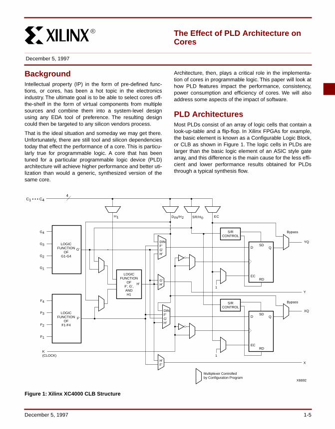
PLD ArchitecturesMost PLDs consist of an array of logic cells that contain alook-up-table and a flip-flop. In Xilinx FPGAs for example,the basic element is known as a Configurable Logic Block,or CLB as shown in Figure 1. The logic cells in PLDs arelarger than the basic logic element of an ASIC style gatearray, and this difference is the main cause for the less effi-cient and lower performance results obtained for PLDsthrough a typical synthesis flow.
LOGICFUNCTION
OFG1-G4
G4
G3
G2
G1
G'
LOGICFUNCTION
OFF1-F4
F4
F3
F2
F1
F'
LOGICFUNCTION
OFF', G',ANDH1
H'
DINF'G'H'
DINF'G'H'
G'H'
H'F'
S/RCONTROL
D
ECRD
Bypass
Bypass
SDYQ
XQ
Q
S/RCONTROL
D
ECRD
SDQ
1
1
K(CLOCK)
Multiplexer Controlledby Configuration Program
Y
X
DIN/H2H1 SR/H0 EC
X6692
C1 • • • C4 4
Figure 1: Xilinx XC4000 CLB Structure
December 5, 1997 1-5
The Effect of PLD Architecture on Cores
There are differences in each PLD vendor’s logic blockstructure as well as differences in features such as I/O andcarry logic, but these involve more detail than will be dealtwith here. Instead, we will focus on differences in routingresources and on-chip RAM since these have the most dra-matic impact on the use of cores.
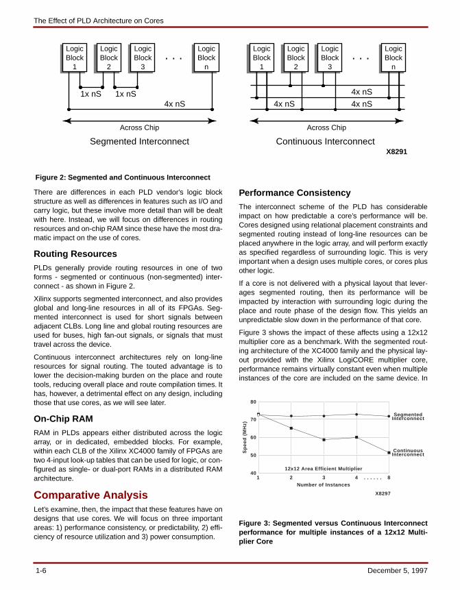
Routing ResourcesPLDs generally provide routing resources in one of twoforms - segmented or continuous (non-segmented) inter-connect - as shown in Figure 2.
Xilinx supports segmented interconnect, and also providesglobal and long-line resources in all of its FPGAs. Seg-mented interconnect is used for short signals betweenadjacent CLBs. Long line and global routing resources areused for buses, high fan-out signals, or signals that musttravel across the device.
Continuous interconnect architectures rely on long-lineresources for signal routing. The touted advantage is tolower the decision-making burden on the place and routetools, reducing overall place and route compilation times. Ithas, however, a detrimental effect on any design, includingthose that use cores, as we will see later.
On-Chip RAMRAM in PLDs appears either distributed across the logicarray, or in dedicated, embedded blocks. For example,within each CLB of the Xilinx XC4000 family of FPGAs aretwo 4-input look-up tables that can be used for logic, or con-figured as single- or dual-port RAMs in a distributed RAMarchitecture.
Comparative AnalysisLet’s examine, then, the impact that these features have ondesigns that use cores. We will focus on three importantareas: 1) performance consistency, or predictability, 2) effi-ciency of resource utilization and 3) power consumption.
Performance ConsistencyThe interconnect scheme of the PLD has considerableimpact on how predictable a core’s performance will be.Cores designed using relational placement constraints andsegmented routing instead of long-line resources can beplaced anywhere in the logic array, and will perform exactlyas specified regardless of surrounding logic. This is veryimportant when a design uses multiple cores, or cores plusother logic.
If a core is not delivered with a physical layout that lever-ages segmented routing, then its performance will beimpacted by interaction with surrounding logic during theplace and route phase of the design flow. This yields anunpredictable slow down in the performance of that core.
Figure 3 shows the impact of these affects using a 12x12multiplier core as a benchmark. With the segmented rout-ing architecture of the XC4000 family and the physical lay-out provided with the Xilinx LogiCORE multiplier core,performance remains virtually constant even when multipleinstances of the core are included on the same device. In
1x nS 1x nS4x nS
LogicBlock
1
LogicBlock
2
LogicBlock
3
LogicBlock
n. . .
Segmented Interconnect Continuous Interconnect
4x nS
4x nS
4x nS
. . .LogicBlock
1
LogicBlock
2
LogicBlock
3
LogicBlock
n
Across Chip Across Chip
X8291
Figure 2: Segmented and Continuous Interconnect
40
50
60
70
80
1 2 3 4 8. . . . . .
12x12 Area Efficient Multiplier
SegmentedInterconnect
ContinuousInterconnect
Number of Instances
Sp
ee
d (
MH
z)
X8297
Figure 3: Segmented versus Continuous Interconnectperformance for multiple instances of a 12x12 Multi-plier Core
1-6 December 5, 1997
contrast, for a PLD with continuous interconnect and coresthat only define logic and not layout, note how performancedegrades considerably as more cores (or additional userdefined logic) are added.
Migrating to a larger device only compounds this problem.Larger devices have longer metal lines with additionalcapacitance. For a segmented architecture, cores thatleverage the interconnect achieve virtually consistent per-formance regardless of the density of the device. In con-trast, cores in a continuous interconnect architecture sufferfrom a 30 percent performance degradation between thesmallest and largest device in the family. This degradationoccurs on top of that shown in Figure 3.
Performance figures for cores in continuous interconnectarchitecture PLDs are usually stated for a single instance ofthat core, implemented in the smallest member of the fam-ily in order to show the highest speed. The problem is that itis impossible to know the actual performance of this coreuntil after the design is placed and routed together with allof the other cores and user logic in the target device.
EfficiencyDevice utilization is a measure of how efficiently a coreuses the logic resources of the PLD. Careful tuning of adesign can yield a dramatic reduction in area, resulting in acore that is both very small, and very fast. PLD architecturecan have a great impact on this as well.
The availability of abundant routing resources helps a lot.Higher densities can be achieved by offering both globaland segmented routing options. Short, isolated signals canbe routed onto local interconnect without wasting longerlines. This option is not available with continuous intercon-nect PLDs.
Many applications, such as in Digital Signal Processing(DSP), take advantage of distributed RAM. PLD-basedDSP uses a unique technique known as distributed arith-metic for which a large array of small RAMs is advanta-geous. PLDs that have no distributed RAM or only blockRAM are limited to using flip-flops. In many cases, thesheer number of flip flops required exceeds the numberavailable in the largest device.
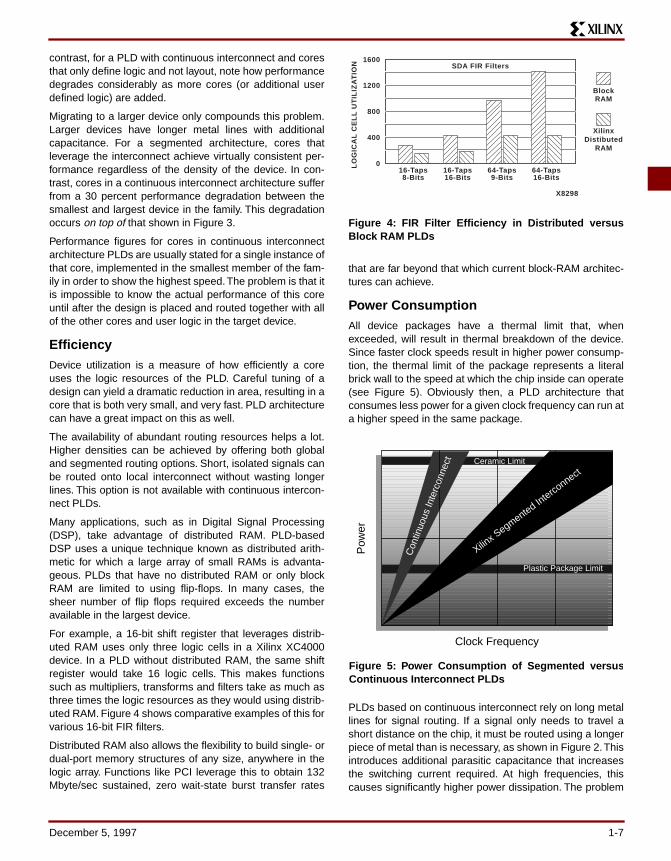
For example, a 16-bit shift register that leverages distrib-uted RAM uses only three logic cells in a Xilinx XC4000device. In a PLD without distributed RAM, the same shiftregister would take 16 logic cells. This makes functionssuch as multipliers, transforms and filters take as much asthree times the logic resources as they would using distrib-uted RAM. Figure 4 shows comparative examples of this forvarious 16-bit FIR filters.
Distributed RAM also allows the flexibility to build single- ordual-port memory structures of any size, anywhere in thelogic array. Functions like PCI leverage this to obtain 132Mbyte/sec sustained, zero wait-state burst transfer rates
that are far beyond that which current block-RAM architec-tures can achieve.
Power ConsumptionAll device packages have a thermal limit that, whenexceeded, will result in thermal breakdown of the device.Since faster clock speeds result in higher power consump-tion, the thermal limit of the package represents a literalbrick wall to the speed at which the chip inside can operate(see Figure 5). Obviously then, a PLD architecture thatconsumes less power for a given clock frequency can run ata higher speed in the same package.
PLDs based on continuous interconnect rely on long metallines for signal routing. If a signal only needs to travel ashort distance on the chip, it must be routed using a longerpiece of metal than is necessary, as shown in Figure 2. Thisintroduces additional parasitic capacitance that increasesthe switching current required. At high frequencies, thiscauses significantly higher power dissipation. The problem
0
400
800
1200
1600SDA FIR Filters
LO
GIC
AL
CE
LL
UT
ILIZ
AT
ION
X8298
16-Taps8-Bits
16-Taps16-Bits
64-Taps9-Bits
64-Taps16-Bits
XilinxDistibuted
RAM
BlockRAM
Figure 4: FIR Filter Efficiency in Distributed versusBlock RAM PLDs
Clock Frequency
Pow
er
Con
tinuo
us In
terc
onne
ct
Xilinx S
egmented Interco
nnect
Plastic Package Limit
Ceramic Limit
Figure 5: Power Consumption of Segmented versu sContinuous Interconnect PLDs
December 5, 1997 1-7
The Effect of PLD Architecture on Cores
only gets worse for higher density devices. This is why highdensity, continuous interconnect PLDs are often only avail-able in large, expensive ceramic packages.
In contrast, a segmented PLD architecture provides theoption to route short distance signals on short pieces ofmetal. This minimizes the load on that signal as well as thecurrent needed to drive it. Cores that are designed usingthe local interconnect of segmented PLDs will consumeless power. This allows the design to run at much higherspeeds for a particular package, or to run at the samespeed and consume less power than possible using a con-tinuous interconnect architecture. The effect of this isshown in Figure 5. The higher efficiencies achieved throughsegmented interconnect and distributed RAM furtherreduce power consumption by allowing a design to beimplemented in a smaller device. This allows even higherperformance as indicated by the ranges shown in the fig-ure.
ConclusionsThe main reason for using cores is to cut development timeand allow designers to focus on those portions of the sys-tem that they know best. Cores are chosen for features,functionality and performance. When it comes to perfor-mance, it is best to know exactly what to expect from a corebefore the design is started. Anything that increases thepossibility of design delays, or even failure, should beavoided.
Xilinx FPGAs, such as the XC4000X architecture, offercapacities reaching the half-million system-gate level.There is no way to maintain the time-to-market value of pro-grammable devices of this capacity efficiently without the
use of cores. Xilinx FPGAs offer superior architectural fea-tures that allow you to implement cores with guaranteedtiming, maximum efficiency and at minimum power allowinghigher performance. This comes as the result of silicon fea-tures that other PLD architectures cannot alter throughupgrades to place and route software.
In addition, all Xilinx LogiCORE functions delivered throughthe CORE Generator tool are unique in that they includeboth the logic and layout required to take advantage of theavailability of segmented routing, distributed RAM andother architectural features not covered in this paper. Thismakes them consistent, predictable and fast while minimiz-ing power consumption.
Finally, Xilinx HardWire products provide the fastest avail-able migration to a true high-volume, low-cost ASIC. Con-version to a HardWire device requires no redesign or testvector generation. In this case, the FPGA serves as theprototype and early production vehicle. Once the FPGAdesign is frozen, Xilinx takes over the conversion processwhile work can begin on the next design. Only Xilinx ownsand offers a risk-free program like this.
No other PLD vendor today offers such a rich set of siliconand software features that makes designing with cores forprogrammable logic so easy. For more information on Xilinxdevices, the CORE Generator tool, or CORE Solutionsproducts, contact your local Xilinx sales representative,send email to [email protected], or look us up on theweb at:
http://www.xilinx.com/products/logicore/logicore.htm
1-8 December 5, 1997
R
XC4000-Series FPGAs: The Best Choice for Delivering Cores
Feb. 8, 1998 XBRF 007 (Version 2.0) Application Brief
SummaryReusable logic provide an efficient means of embedding common logic functions in high-density FPGA designs. The richfeature set of the XC4000-Series FPGA devices makes them the ideal choice for core-based system design.
Xilinx FamilyXC4000E, XC4000EX, XC4000XL, XC4000XV
IntroductionReusable designs, called cores, have been available todesigners using traditional mask-programmed gate arraysfor several years. Typically, these cores are pre-designed,pre-tested implementations of widely-used system func-tions that can be “dropped” into a design and integratedwith the application-specific functions of that design. Exam-ples of functions commonly available as cores include businterfaces, microcontrollers, and DSP functions such asdigital filters. The use of such pre-designed modules accel-erates time-to- market and allows the designer to focus hisor her time and resources on the system’s unique func-tions.
Now that Field Programmable Gate Arrays (FPGAs) havereached usable densities in the hundreds of thousands ofgates, FPGAs have become an ideal “platform” for thedevelopment and use of cores and other intellectual prop-erty. Specifically, the Xilinx XC4000-Series FPGAs, con-sisting of the XC4000E, XC4000EX, XC4000XL andXC4000XV family devices, deliver the best combination ofperformance, density, features, and flexibility to support theuse of cores in high-density FPGA design.
Today’s designer can select from a variety of high-densityFPGA devices and architectures. However, the successfulimplementation of system-level designs requires muchmore than just “raw gates”. The FPGA architecture mustinclude the system-integration features that allow the effi-cient integration of pre-defined cores and application-spe-cific functions. The XC4000-Series is unique in itsincorporation of so many of the features required for thesuccessful implementation and use of cores.
XC4000 Architectural FeaturesThe XC4000-Series silicon provides more that just gatesand flip-flops—it provides a system-level solution. The fol-lowing represent unique XC4000 FPGA features.
Flexible ClockingClock structures are important, especially in high-densitydesigns. The XC4000-Series offers up to eight dedicated
low-skew, high fan-out clock distribution networks. Any, orall, of the flip-flops can be driven from one of these net-works.
However, some applications require more than eightclocks. Each XC4000-Series logic block clock input can bedriven by an individual clock signal, allowing literally hun-dreds of clocks in a single design.
Advanced On-Chip RAM (and ROM)Many systems require RAM memory, either as standardread/write memory or as FIFOs. XC4000-Series FPGAsprovide ample distributed SelectRAM to build small blocksof efficient storage on-chip. On-chip RAM results in betterintegration and improved system performance.
The XC4000-Series RAM is included in every logic block.Larger memory arrays are built by connecting multiple logicblocks together. Each memory array optimally uses theavailable device resources. In contrast, FPGAs with onlylarge dedicated RAM blocks often suffer from poor effi-ciency. Not every design uses all of the RAM available in alarge block. Xilinx was first to provide on-chip RAM in a pro-grammable logic device. Since then, other vendors havefollowed, but do not offer the XC4000’s advanced RAM fea-tures.
XC4000-Series RAM supports true dual-port access, pro-viding superior performance in FIFO and data bufferingapplications. The XC4000 software provides a memorycompiler to quickly and easily build large RAM arrays. Plus,the memory compiler can also build ROM structures forimplementing control stores, system configuration informa-tion, or state machine code.
Internal Bi-Directional BussingMost system-level designs contain a bi-directional databus. Consequently, the XC4000-Series provides an effi-cient internal bussing structure for optimal bi-directionaldata flow within the device. In other FPGA technologies,busses must be re-implemented using multiplexers. Buses
Feb. 8, 1998 XBRF 007 (Version 2.0) 1-9
XC4000-Series FPGAs: The Best Choice for Delivering Cores
implemented using multiplexers consume more resources,resulting in slower system performance.
Numerous and Flexible Output EnablesLarge system designs typically require bi-directional I/O.These three-state outputs are controlled by an outputenable signal. The XC4000-Series FPGAs provide up toone output-enable per I/O for maximum flexibility. Theseoutput-enables are plentiful and operate independently ofthe clock resources. A Global Three-State forces all outputsto high-impedance for test purposes or for power-on resetfunctions.
Definable Power-Up StateIn many applications, the power-up state of the design isimportant. Enable lines must be held disabled until theremainder of the system is functioning. Counters mustpower-up in a known state.
The XC4000-Series FPGAs automatically initialize all ofthe device flip-flops to a specified state on power-up or aftera Global Reset. Each flip-flop can be individually pro-grammed to power-up in the set or reset state.
Furthermore, each of the XC4000 I/O pins can be config-ured with either a pull-up or pull-down resistor, holdingthem at a pre-determined logic level until driven.
Built-in JTAG SupportJTAG (IEEE 1148.1) test logic is an important considerationfor high-density system designs, especially when usingaggressive surface-mount technology like Ball Grid Arrays.The XC4000-Series FPGAs have JTAG support built intoevery device. No additional logic is required.
ReprogrammableXC4000 FPGAs are infinitely reprogrammable—even insystem. Design modifications can be made quickly andeasily, without throwing away devices. A design in the fieldcan even be enhanced with new features or designupdates.
XC4000-Series Product Features
Scalable, Broad Product FamilyThe XC4000-Series is the world’s most-popular and theindustry’s broadest FPGA family. Its scalable architectureand design software provide system solutions ranging from3,000 gates up to 500,000 gates and beyond, offering theultimate in design flexibility. An XC4000-based core can beintegrated with the user’s application and migrated between
a wide range of devices, providing the right solution for thedesign.
Advanced Packaging, Footprint CompatibilityThe XC4000-Series devices are available in a wide varietyof packaging options, including pin grid array, ball gridarray, quad flat pack, and thin quad flat pack. Furthermore,there is footprint compatibility between various XC4000device densities in the same package plus compatibilitywith other Xilinx logic technologies. This allows thedesigner to migrate to higher density devices without hav-ing to change the board layout.
Pinout StabilityOften, the design and procurement of the printed circuitboard (PCB) is in the critical path for completion of a sys-tem design. Thus, designers prefer to fix the pinout of theirFPGAs early in the design cycle and maintain that pinoutconfiguration during subsequent design iterations.
The XC4000-Series devices have extra interconnectaround the periphery of the device to enhance pinout stabil-ity between design revisions. In contrast, other FPGAs cabecome “unroutable” as a result of even small designchanges if the pinouts are locked in place.
High QualityXC4000-Series FPGAs are 100%-tested standard prod-ucts manufactured in high volumes with significantly higherquality than that achievable in most ASIC designs.
Proven Risk-Free Cost-Reduction PathFor high-volume applications, a thoroughly system-verifiedFPGA design can be cost-reduced using Xilinx HardWiretechnology. The HardWire conversion process offers risk-free 100% pin- and function-compatibility with the equiva-lent FPGA device, preserving the same PC board. Plus,thorough test vectors are generated automatically, saving
the engineer from creating complex simulation files. WithHardWire technology, the engineer needs to design theXC4000-Series FPGAs: The Best Choice for DeliveringLogic Cores, system only once. There is no need to rede-sign specifically for another technology.
XC4000 Design SoftwareSuccessfully implementing a design requires more thanjust silicon. Design software is an important considerationin any logic design. Xilinx offers complete software devel-opment solutions which enable the implementation ofdesigns in Xilinx Programmable Logic devices.
1-10
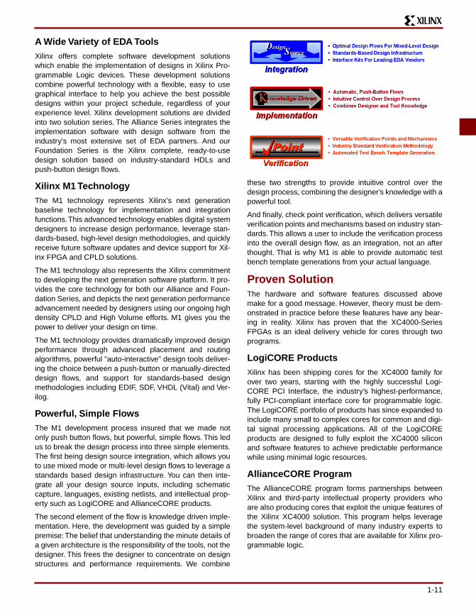
A Wide Variety of EDA ToolsXilinx offers complete software development solutionswhich enable the implementation of designs in Xilinx Pro-grammable Logic devices. These development solutionscombine powerful technology with a flexible, easy to usegraphical interface to help you achieve the best possibledesigns within your project schedule, regardless of yourexperience level. Xilinx development solutions are dividedinto two solution series. The Alliance Series integrates theimplementation software with design software from theindustry's most extensive set of EDA partners. And ourFoundation Series is the Xilinx complete, ready-to-usedesign solution based on industry-standard HDLs andpush-button design flows.
Xilinx M1 TechnologyThe M1 technology represents Xilinx's next generationbaseline technology for implementation and integrationfunctions. This advanced technology enables digital systemdesigners to increase design performance, leverage stan-dards-based, high-level design methodologies, and quicklyreceive future software updates and device support for Xil-inx FPGA and CPLD solutions.
The M1 technology also represents the Xilinx commitmentto developing the next generation software platform. It pro-vides the core technology for both our Alliance and Foun-dation Series, and depicts the next generation performanceadvancement needed by designers using our ongoing highdensity CPLD and High Volume efforts. M1 gives you thepower to deliver your design on time.
The M1 technology provides dramatically improved designperformance through advanced placement and routingalgorithms, powerful "auto-interactive" design tools deliver-ing the choice between a push-button or manually-directeddesign flows, and support for standards-based designmethodologies including EDIF, SDF, VHDL (Vital) and Ver-ilog.
Powerful, Simple FlowsThe M1 development process insured that we made notonly push button flows, but powerful, simple flows. This ledus to break the design process into three simple elements.The first being design source integration, which allows youto use mixed mode or multi-level design flows to leverage astandards based design infrastructure. You can then inte-grate all your design source inputs, including schematiccapture, languages, existing netlists, and intellectual prop-erty such as LogiCORE and AllianceCORE products.
The second element of the flow is knowledge driven imple-mentation. Here, the development was guided by a simplepremise: The belief that understanding the minute details ofa given architecture is the responsibility of the tools, not thedesigner. This frees the designer to concentrate on designstructures and performance requirements. We combine
these two strengths to provide intuitive control over thedesign process, combining the designer’s knowledge with apowerful tool.
And finally, check point verification, which delivers versatileverification points and mechanisms based on industry stan-dards. This allows a user to include the verification processinto the overall design flow, as an integration, not an afterthought. That is why M1 is able to provide automatic testbench template generations from your actual language.
Proven SolutionThe hardware and software features discussed abovemake for a good message. However, theory must be dem-onstrated in practice before these features have any bear-ing in reality. Xilinx has proven that the XC4000-SeriesFPGAs is an ideal delivery vehicle for cores through twoprograms.
LogiCORE ProductsXilinx has been shipping cores for the XC4000 family forover two years, starting with the highly successful Logi-CORE PCI Interface, the industry’s highest-performance,fully PCI-compliant interface core for programmable logic.The LogiCORE portfolio of products has since expanded toinclude many small to complex cores for common and digi-tal signal processing applications. All of the LogiCOREproducts are designed to fully exploit the XC4000 siliconand software features to achieve predictable performancewhile using minimal logic resources.
AllianceCORE ProgramThe AllianceCORE program forms partnerships betweenXilinx and third-party intellectual property providers whoare also producing cores that exploit the unique features ofthe Xilinx XC4000 solution. This program helps leveragethe system-level background of many industry experts tobroaden the range of cores that are available for Xilinx pro-grammable logic.
1-11

XC4000-Series FPGAs: The Best Choice for Delivering Cores
Support
World-Class Technical SupportA working design takes more than silicon and software. Itsometime takes support, too. Xilinx is committed to provid-
ing world-class technical support through its world-widenetwork of expert field applications engineers, telephonehotline support engineers, World-Wide Web and E-maillinks, design center, and training classes.
1-12
R
Product Listing by Application Segment
February 8, 1998
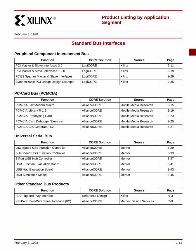
Standard Bus Interfaces
Peripheral Component Interconnect Bus
Function CORE Solution Source Page
PCI Master & Slave Interfaces 2.0 LogiCORE Xilinx 2-11
PCI Master & Slave Interfaces 1.2.0 LogiCORE Xilinx 2-19
PCI32 Spartan Master & Slave Interfaces LogiCORE Xilinx 2-29
Synthesizable PCI Bridge Design Example LogiCORE Xilinx 2-35
PC-Card Bus (PCMCIA)
Function CORE Solution Source Page
PCMCIA Fax/Modem Macro AllianceCORE Mobile Media Research 3-15
PCMCIA Library R 1.2 AllianceCORE Mobile Media Research 3-19
PCMCIA Prototyping Card AllianceCORE Mobile Media Research 3-23
PCMCIA Card Debugger/Exerciser AllianceCORE Mobile Media Research 3-25
PCMCIA CIS Generator 1.2 AllianceCORE Mobile Media Research 3-27
Universal Serial Bus
Function CORE Solution Source Page
Low-Speed USB Function Controller AllianceCORE Mentor 3-29
Full-Speed USB Function Controller AllianceCORE Mentor 3-33
3-Port USB Hub Controller AllianceCORE Mentor 3-37
USB Function Evaluation Board AllianceCORE Mentor 3-41
USB Hub Evaluation Board AllianceCORE Mentor 3-43
USB Simulation Model AllianceCORE Mentor 3-45
Other Standard Bus Products
Function CORE Solution Source Page
ISA Plug and Play Interface Reference Design Xilinx 5-3
XF-TWSI Two-Wire Serial Interface (IIC) AllianceCORE Memec Design Services 3-9
February 8, 1998 1-13
Product Listing by Application Segment
Digital Signal Processing
Communications and Networking
Correlators
Function CORE Solution Source Page
One Dimensional RAM-Based Correlator LogiCORE Xilinx 2-45
One Dimensional ROM-Based Correlator LogiCORE Xilinx 2-41
Filters
Function CORE Solution Source Page
Comb Filter LogiCORE Xilinx 2-49
16-Tap, 8-Bit FIR Filter Reference Design Xilinx 5-3
Serial Distributed Arithmetic FIR Filter LogiCORE Xilinx 2-51
Dual-Channel Serial Distributed Arithmetic FIR Filter
LogiCORE Xilinx 2-55
Parallel Distributed Arithmetic FIR Filter LogiCORE Xilinx 2-59
Transforms
Function CORE Solution Source Page
DFT Core (Real Data In, Complex Data Out) LogiCORE Xilinx 2-65
FFT Core (1024 Points) LogiCORE Xilinx 2-69
DSP Building Blocks
Function CORE Solution Source Page
SDA FIR Control Logic LogiCORE Xilinx 2-73
Sine/Cosine LogiCORE Xilinx 2-75
Non-Symmetric, 16-Deep Time Skew Buffer LogiCORE Xilinx 2-77
Non-Symmetric, 32-Deep Time Skew Buffer LogiCORE Xilinx 2-81
Symmetric, 16-Deep Time Skew Buffer LogiCORE Xilinx 2-85
Asynchronous Transfer Mode
Function CORE Solution Source Page
Cell Assembler (CC-201) AllianceCORE CoreEl Microsystems 3-49
Cell Delineation (CC-200) AllianceCORE CoreEl Microsystems 3-53
CRC10 Generator and Verifier (CC-130) AllianceCORE CoreEl Microsystems 3-57
CRC32 Generator and Verifier (CC-131) AllianceCORE CoreEl Microsystems 3-61
UTOPIA Slave (CC-141) AllianceCORE CoreEl Microsystems 3-85
1-14 February 8, 1998
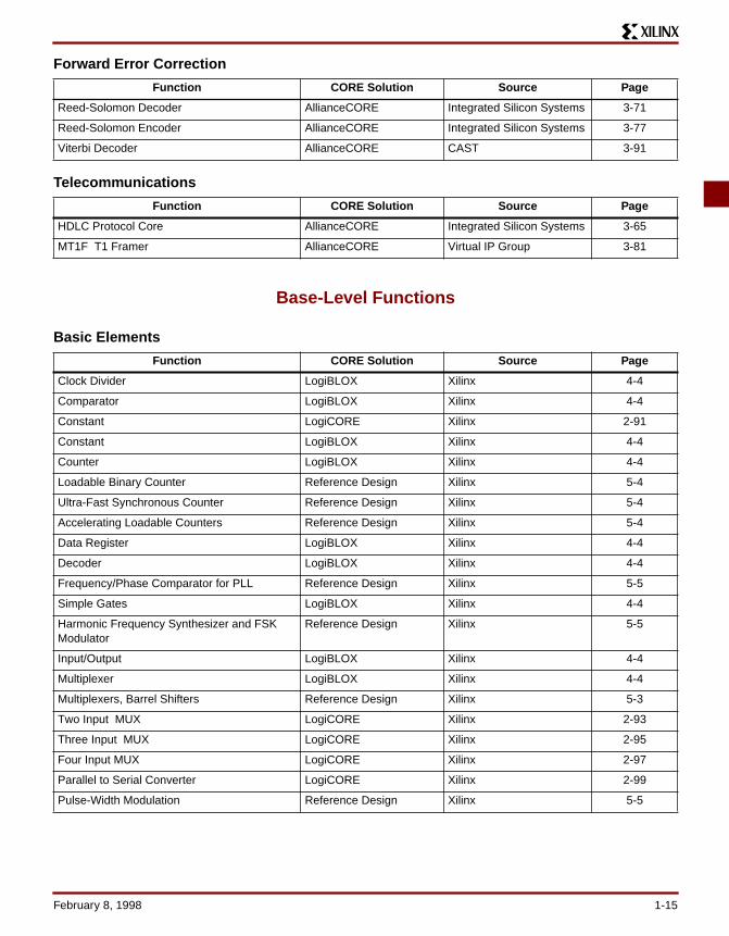
Base-Level Functions
Forward Error Correction
Function CORE Solution Source Page
Reed-Solomon Decoder AllianceCORE Integrated Silicon Systems 3-71
Reed-Solomon Encoder AllianceCORE Integrated Silicon Systems 3-77
Viterbi Decoder AllianceCORE CAST 3-91
Telecommunications
Function CORE Solution Source Page
HDLC Protocol Core AllianceCORE Integrated Silicon Systems 3-65
MT1F T1 Framer AllianceCORE Virtual IP Group 3-81
Basic Elements
Function CORE Solution Source Page
Clock Divider LogiBLOX Xilinx 4-4
Comparator LogiBLOX Xilinx 4-4
Constant LogiCORE Xilinx 2-91
Constant LogiBLOX Xilinx 4-4
Counter LogiBLOX Xilinx 4-4
Loadable Binary Counter Reference Design Xilinx 5-4
Ultra-Fast Synchronous Counter Reference Design Xilinx 5-4
Accelerating Loadable Counters Reference Design Xilinx 5-4
Data Register LogiBLOX Xilinx 4-4
Decoder LogiBLOX Xilinx 4-4
Frequency/Phase Comparator for PLL Reference Design Xilinx 5-5
Simple Gates LogiBLOX Xilinx 4-4
Harmonic Frequency Synthesizer and FSK Modulator
Reference Design Xilinx 5-5
Input/Output LogiBLOX Xilinx 4-4
Multiplexer LogiBLOX Xilinx 4-4
Multiplexers, Barrel Shifters Reference Design Xilinx 5-3
Two Input MUX LogiCORE Xilinx 2-93
Three Input MUX LogiCORE Xilinx 2-95
Four Input MUX LogiCORE Xilinx 2-97
Parallel to Serial Converter LogiCORE Xilinx 2-99
Pulse-Width Modulation Reference Design Xilinx 5-5
February 8, 1998 1-15
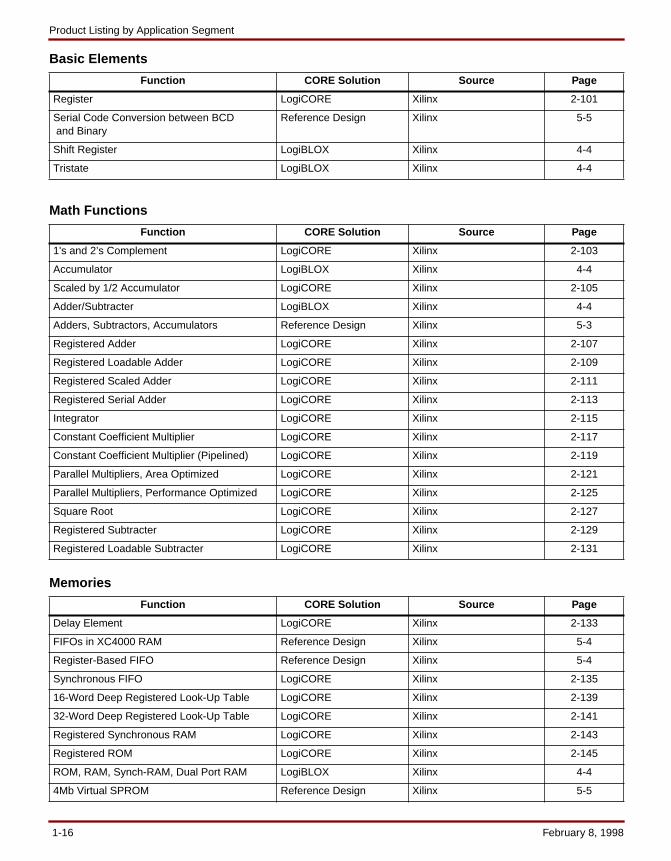
Product Listing by Application Segment
Function CORE Solution Source Page
Register LogiCORE Xilinx 2-101
Serial Code Conversion between BCD and Binary
Reference Design Xilinx 5-5
Shift Register LogiBLOX Xilinx 4-4
Tristate LogiBLOX Xilinx 4-4
Math Functions
Function CORE Solution Source Page
1's and 2’s Complement LogiCORE Xilinx 2-103
Accumulator LogiBLOX Xilinx 4-4
Scaled by 1/2 Accumulator LogiCORE Xilinx 2-105
Adder/Subtracter LogiBLOX Xilinx 4-4
Adders, Subtractors, Accumulators Reference Design Xilinx 5-3
Registered Adder LogiCORE Xilinx 2-107
Registered Loadable Adder LogiCORE Xilinx 2-109
Registered Scaled Adder LogiCORE Xilinx 2-111
Registered Serial Adder LogiCORE Xilinx 2-113
Integrator LogiCORE Xilinx 2-115
Constant Coefficient Multiplier LogiCORE Xilinx 2-117
Constant Coefficient Multiplier (Pipelined) LogiCORE Xilinx 2-119
Parallel Multipliers, Area Optimized LogiCORE Xilinx 2-121
Parallel Multipliers, Performance Optimized LogiCORE Xilinx 2-125
Square Root LogiCORE Xilinx 2-127
Registered Subtracter LogiCORE Xilinx 2-129
Registered Loadable Subtracter LogiCORE Xilinx 2-131
Basic Elements
Memories
Function CORE Solution Source Page
Delay Element LogiCORE Xilinx 2-133
FIFOs in XC4000 RAM Reference Design Xilinx 5-4
Register-Based FIFO Reference Design Xilinx 5-4
Synchronous FIFO LogiCORE Xilinx 2-135
16-Word Deep Registered Look-Up Table LogiCORE Xilinx 2-139
32-Word Deep Registered Look-Up Table LogiCORE Xilinx 2-141
Registered Synchronous RAM LogiCORE Xilinx 2-143
Registered ROM LogiCORE Xilinx 2-145
ROM, RAM, Synch-RAM, Dual Port RAM LogiBLOX Xilinx 4-4
4Mb Virtual SPROM Reference Design Xilinx 5-5
1-16 February 8, 1998
Processor Products
Function CORE Solution Source Page
Dynamic Microcontroller Reference Design Xilinx 5-4
TX400 Series RISC CPU Cores AllianceCORE T7L Technology Inc. 3-97
RISC CPU Core Design Base Board AllianceCORE T7L Technology Inc. 3-103
Scalable Development Platform Integrated Software
AllianceCORE T7L Technology Inc. 3-107
V8 uRISC 8-bit RISC Microprocessor AllianceCORE VAutomation 3-109
IntelliCoreTM Prototyping System AllianceCORE VAutomation 3-115
Processor Peripherals
Function CORE Solution Source Page
C2910A Microprogram Controller AllianceCORE CAST 3-129
Configuring FPGAs over a Processor Bus Reference Design Xilinx 5-5
M8237 DMA Controller AllianceCORE Virtual IP Group 3-133
M8254 Programmable Timer AllianceCORE Virtual IP Group 3-143
M8255 Programmable Peripheral Interface AllianceCORE Virtual IP Group 3-147
XF8255 Programmable Peripheral Interface AllianceCORE Memec Design Services 3-151
XF8256 Multifunction Microprocessor Support Controller
AllianceCORE Memec Design Services 3-155
M8259 Programmable Interrupt Controller AllianceCORE Virtual IP Group 3-159
XF8279 Programmable Keyboard Display In-terface
AllianceCORE Memec Design Services 3-163
XF9128 Video Terminal Logic Controller AllianceCORE Memec Design Services 3-167
DRAM Controller AllianceCORE NMI Electronics 3-173
UARTs
Function CORE Solution Source Page
XF-8250 Asynchronous Communications Ele-ment
AllianceCORE Memec Design Services 3-137
M16450 - Universal Asynchronous Receiver/Transmitter
AllianceCORE Virtual IP Group 3-121
M16550A - UART With RAM AllianceCORE Virtual IP Group 3-125
Generic Development Tools
Function CORE Solution Source Page
GVA-100 DSP Prototyping Platform AllianceCORE GV & Associates 3-179
MDS FPGA Development Module AllianceCORE Memec Design Services 3-183
Microprocessor-Based Core Evaluation Card AllianceCORE NMI Electronics 3-185
Xilinx CORE Generator LogiCORE Xilinx 2-7
February 8, 1998 1-17
Product Listing by Application Segment
1-18 February 8, 1998
LogiCORE Products
1. Introduction
2. LogiCORE Products
3. AllianceCORE Products
4. LogiBLOX
5. Reference Designs
2-1
February 8, 1998
LogiCORE Products Table of Contents
LogiCORE ProductsProduct Overview . . . . . . . . . . . . . . . . . . . . . . . . . . . . . . . . . . . . . . . . . . . . . . . . . . .2-5Xilinx CORE Generator . . . . . . . . . . . . . . . . . . . . . . . . . . . . . . . . . . . . . . . . . . . . . .2-7
Peripheral Component Interconnect Bus Table of Contents . . . . . . . . . . . . . . . . . .2-9PCI Master & Slave Interfaces Version 2.0 . . . . . . . . . . . . . . . . . . . . . . . . . . . . . .2-11PCI Master & Slave Interfaces Version 1.2.0 . . . . . . . . . . . . . . . . . . . . . . . . . . . . .2-19PCI32 Spartan Master & Slave Interfaces . . . . . . . . . . . . . . . . . . . . . . . . . . . . . . .2-29Synthesizable PCI Bridge Design Example . . . . . . . . . . . . . . . . . . . . . . . . . . . . . .2-35
Digital Signal Processing Table of Contents . . . . . . . . . . . . . . . . . . . . . . . . . . . . . .2-39CorrelatorsOne Dimensional ROM-Based Correlator . . . . . . . . . . . . . . . . . . . . . . . . . . . . . . .2-41One Dimensional RAM-Based Correlator . . . . . . . . . . . . . . . . . . . . . . . . . . . . . . .2-45FiltersComb Filter . . . . . . . . . . . . . . . . . . . . . . . . . . . . . . . . . . . . . . . . . . . . . . . . . . . . . . .2-49Serial Distributed Arithmetic FIR Filter . . . . . . . . . . . . . . . . . . . . . . . . . . . . . . . . . .2-51Dual-Channel Serial Distributed Arithmetic FIR Filter . . . . . . . . . . . . . . . . . . . . . .2-55Parallel Distributed Arithmetic FIR Filter . . . . . . . . . . . . . . . . . . . . . . . . . . . . . . . .2-59TransformsDFT Cores (Real Data In, Complex Data Out) . . . . . . . . . . . . . . . . . . . . . . . . . . . .2-65FFT Core (1024 Points) . . . . . . . . . . . . . . . . . . . . . . . . . . . . . . . . . . . . . . . . . . . .2-69DSP Building BlocksSDA FIR Control Logic . . . . . . . . . . . . . . . . . . . . . . . . . . . . . . . . . . . . . . . . . . . . . .2-73Sine/Cosine . . . . . . . . . . . . . . . . . . . . . . . . . . . . . . . . . . . . . . . . . . . . . . . . . . . . . .2-75Non-Symmetric, 16-Deep Time Skew Buffer . . . . . . . . . . . . . . . . . . . . . . . . . . . . .2-77Non-Symmetric, 32-Deep Time Skew Buffer . . . . . . . . . . . . . . . . . . . . . . . . . . . . .2-81Symmetric, 16-Deep Time Skew Buffer . . . . . . . . . . . . . . . . . . . . . . . . . . . . . . . . .2-85
Base-Level Functions Table of Contents . . . . . . . . . . . . . . . . . . . . . . . . . . . . . . . . .2-89Basic ElementsConstant . . . . . . . . . . . . . . . . . . . . . . . . . . . . . . . . . . . . . . . . . . . . . . . . . . . . . . . . .2-91Two Input MUX . . . . . . . . . . . . . . . . . . . . . . . . . . . . . . . . . . . . . . . . . . . . . . . . . . .2-93Three Input MUX . . . . . . . . . . . . . . . . . . . . . . . . . . . . . . . . . . . . . . . . . . . . . . . . . .2-95Four Input MUX . . . . . . . . . . . . . . . . . . . . . . . . . . . . . . . . . . . . . . . . . . . . . . . . . . .2-97Parallel to Serial Converter . . . . . . . . . . . . . . . . . . . . . . . . . . . . . . . . . . . . . . . . . .2-99Register . . . . . . . . . . . . . . . . . . . . . . . . . . . . . . . . . . . . . . . . . . . . . . . . . . . . . . . .2-101Math Functions1’s and 2’s Complement . . . . . . . . . . . . . . . . . . . . . . . . . . . . . . . . . . . . . . . . . . . .2-103Scaled By 1/2 Accumulator . . . . . . . . . . . . . . . . . . . . . . . . . . . . . . . . . . . . . . . . .2-105Registered Adder . . . . . . . . . . . . . . . . . . . . . . . . . . . . . . . . . . . . . . . . . . . . . . . . .2-107Registered Loadable Adder . . . . . . . . . . . . . . . . . . . . . . . . . . . . . . . . . . . . . . . . .2-109Registered Scaled Adder . . . . . . . . . . . . . . . . . . . . . . . . . . . . . . . . . . . . . . . . . . 2-111Registered Serial Adder . . . . . . . . . . . . . . . . . . . . . . . . . . . . . . . . . . . . . . . . . . . 2-113
2-2 February 8, 1998
Integrator . . . . . . . . . . . . . . . . . . . . . . . . . . . . . . . . . . . . . . . . . . . . . . . . . . . . . . .2-115Constant Coefficient Multiplier . . . . . . . . . . . . . . . . . . . . . . . . . . . . . . . . . . . . . . .2-117Constant Coefficient Multiplier (Pipelined) . . . . . . . . . . . . . . . . . . . . . . . . . . . . . 2-119Parallel Multipliers - Area Optimized. . . . . . . . . . . . . . . . . . . . . . . . . . . . . . . . . . 2-121Parallel Multipliers - Performance Optimized . . . . . . . . . . . . . . . . . . . . . . . . . . . 2-125Square Root . . . . . . . . . . . . . . . . . . . . . . . . . . . . . . . . . . . . . . . . . . . . . . . . . . . . .2-127Registered Subtracter . . . . . . . . . . . . . . . . . . . . . . . . . . . . . . . . . . . . . . . . . . . . . 2-129Registered Loadable Subtracter . . . . . . . . . . . . . . . . . . . . . . . . . . . . . . . . . . . . . 2-131MemoriesDelay Element . . . . . . . . . . . . . . . . . . . . . . . . . . . . . . . . . . . . . . . . . . . . . . . . . . .2-133Synchronous FIFO . . . . . . . . . . . . . . . . . . . . . . . . . . . . . . . . . . . . . . . . . . . . . . . .2-13516-Word Deep Registered Look-Up Table . . . . . . . . . . . . . . . . . . . . . . . . . . . . . 2-13932-Word Deep Registered Look-Up Table . . . . . . . . . . . . . . . . . . . . . . . . . . . . . 2-141Registered Synchronous RAM . . . . . . . . . . . . . . . . . . . . . . . . . . . . . . . . . . . . . . 2-143Registered ROM . . . . . . . . . . . . . . . . . . . . . . . . . . . . . . . . . . . . . . . . . . . . . . . . .2-145
February 8, 1998 2-3

LogiCORE Products Table of Contents
2-4 February 8, 1998
Product Overview
February 8, 1998
LogiCORE ProductsLogiCORE products are sold, licensed and supported byXilinx. They are developed internally by Xilinx or jointly witha partner.
The cores that Xilinx provides as LogiCORE products typi-cally fall into one of two categories. The first are high-per-formance interface cores that require a thoroughunderstanding and control of the FPGA technology andimplementation software in order to achieve the desiredperformance and complexity. An example of a core in thiscategory is the LogiCORE PCI interface.
The second category are cores that benefit from a veryspecialized implementation in the FPGA. An example is theLogiCORE DSP modules that are implemented using aunique algorithm, Distributed Arithmetic. This algorithm fitsthe lookup-table-based architecture of the FPGA. Theresult is outstanding performance and device utilization,often more than 10 times better than generic HDL descrip-tions.
Xilinx CORE GeneratorIn addition to actual cores, Xilinx is committed to developenabling design tools and methodologies to facilitate usageof cores with FPGAs. The first of this product type is theCORE Generator tool. This innovative methodology foracquiring and using cores allow to combine the benefits of1) a firm core with predictable performance, and 2) the flex-ibility of system level design, facilitated by behavioraldescription languages such as VHDL and Verilog.
LogiCORE products are customized to fit your specificapplication using an intuitive graphical user interface.Based on your inputs, the CORE Generator generates aproven core with predictable timing that can be integratedusing a VHDL-, Verilog- or schematic-based design flow. Asa result, you can put several, individually proven cores withgiven performance, into one system on a single FPGA.Because each core is already verified, the time-to-marketbenefits are maintained for high-complexity FPGAs.
Xilinx PCI solutionsThe Xilinx PCI solution includes the necessary devices,tools and cores to build a cost-effective single-chip PCI sys-tem in record time.
• LogiCORE PCI - the highest performing PCI core with predictable timing
• XC4000E/XLT - the industry’s fastest FPGAs that allow
you to integrate a PCI interface plus 5 to 60 thousand gates
• Spartan - the industry’s lowest cost FPGA; on-chip RAM allows high performance for the most cost-effective programmable solution for PCI.
• HardWire - an automatic migration path to a low-cost chip for volume production
• Web-based configuration - for easy configuration and integration of the LogiCORE PCI module
• 3rd party Design Centers - with PCI expertise available for special applications and customization of the core
PCI is an extremely high-performance and complex specifi-cation that is challenging to meet in any technology. Tomeet the stringent PCI specification the core is carefullyhand-tuned for the targeted architecture. Placement androuting for the critical parts of the core are locked down toensure that timing can be met every time the core areimplemented.
To achieve our goals, the LogiCORE development team isworking closely with both IC and Software teams. Newmethodologies for characterizing and modeling our FPGAshave been developed as a result of this teamwork. You willhave access to state of the art technology and expertise,allowing you to complete your PCI application in recordtime.
Xilinx has sold hundreds of LogiCORE PCI licenses andhas built up a solid knowledge about PCI. We are commit-ted, and will continuously improve our PCI products toremain state of the art.
Xilinx DSP SolutionsUsing an FPGA to implement DSP functions often allow aradical performance advantage over fixed processors whilemaintaining maximum flexibility and shortest time-to-mar-ket. Until now, tools to automate the design process havebeen lacking and most designs have been completed man-ually by experienced FPGA designers.
Xilinx’ DSP LogiCORE products are complex parameter-ized DSP building blocks that deliver performance and den-sity equal to or better then a hand-tuned implementation.LogiCORE DSP modules can be used with VHDL, Verilogor schematic capture design methodologies.
Higher level DSP cores are available from our Alli-anceCORE partners.
February 8, 1998 2-5
Product OverviewProduct Overview
Acquiring LogiCORE ProductsLogiCORE products are available from your local Xilinxsales representative similar to other Xilinx software prod-ucts. Xilinx and your local sales representative will also beyour primary source for support of the core, the devices
and the design tools. You can also send email questions to:[email protected].
2-6 February 8, 1998
Xilinx CORE Generator
January 28, 1998 Preliminary V1.0
Xilinx Inc.2100 Logic DriveSan Jose, CA 95124Phone: +1 408-559-7778Fax: +1 408-559-7114E-mail: [email protected]: www.xilinx.com
R
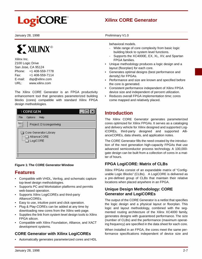
The Xilinx CORE Generator is an FPGA productivityenhancement tool that generates parameterized buildingblocks (cores) compatible with standard Xilinx FPGAdesign methodologies.
Figure 1: The CORE Generator Window
Features• Compatible with VHDL, Verilog, and schematic capture
top-level design methodologies.• Supports PC and Workstation platforms and permits
web-based operation.• Supports Xilinx LogiCOREs and third-party
AllianceCOREs.• Easy to use, intuitive point and click operation.• Plug & Play-COREs can be added at any time by
downloading new cores from the Xilinx web page. • Supplies the link from system level design tools to Xilinx
FPGA silicon.• Compatible with Xilinx Foundation, Alliance, and XACT
development systems.
CORE Generator with Xilinx LogiCOREs• Automatically generates parameterized cores and HDL
behavioral models.- Wide range of core complexity from basic logic
building block to system level functions.- Supports the XC4000E, EX, XL, XV, and Spartan
FPGA families.• Unique methodology produces a logic design and a
layout (floorplan) for each core.• Generates optimal designs (best performance and
density) for FPGAs. • Performance and size are known and specified before
the core is generated.• Consistent performance independent of Xilinx FPGA
device size and independent of percent utilization.• Reduces overall FPGA implementation time; cores
come mapped and relatively placed.
IntroductionThe Xilinx CORE Generator generates parameterizedcores optimized for Xilinx FPGAs. It serves as a catalogingand delivery vehicle for Xilinx designed and supported Log-iCOREs, third-party designed and supported Alli-anceCOREs, data sheets, and application notes.
The CORE Generator fills the need created by the introduc-tion of the next generation high-capacity FPGAs that useadvanced semiconductor process technology. A 100,000-gate design can be built from a collection of cores in a mat-ter of hours.
FPGA LogiCORE: Matrix of CLBsXilinx FPGAs consist of an expandable matrix of “Config-urable Logic Blocks” (CLBs). A LogiCORE is delivered asa pre-defined group of CLBs that maintain their relativelocations when placed anywhere in an FPGA.
Unique Design Methodology: CORE Generator and LogiCOREsThe output of the CORE Generator is a netlist that specifiesthe logic design and a physical layout or floorplan. Thislogic and layout methodology, combined with the seg-mented routing architecture of the Xilinx XC4000 family,generates designs with guaranteed performance. The size(number of CLBs) and the performance (maximum operat-ing frequency) are specified in the data sheet for each core.
When installed in an FPGA, the cores meet the same per-formance specifications independent of device size and
January 28, 1998 2-7
Xilinx CORE GeneratorXilinx CORE Generator
independent of how many cores are used in a large FPGAdevice.
Traditionally, cores for most other FPGAs are “soft” coresbecause the physical layout and characteristics of thedesign cannot be known prior to placement and routing.Every placement and routing iteration results in a differentphysical layout and as a result, the performance is not pre-dictable.
The CORE Generator takes advantage of the Xilinx seg-mented architecture and does not use any of the globalrouting resources except for the global clock distributionnetwork. The core can be placed anywhere in any sizeFPGA and then interconnected with standard routing soft-ware. The performance will always be the same for a givenspeed device.
Without this predictability it is not possible to know whethera design will work until the final phases of a project, when itmay be too late to move to an alternative approach. Withthe CORE Generator approach, the theoretical designmatches the actual design.
Designs optimized for FPGAsThe CORE Generator produces designs that are optimizedfor FPGAs in two ways. First, the LogiCORE implementa-tions are generated with FPGA architecture in mind andtake advantage of the look-up table logic and distributedRAM. Second, they include mapping information and rela-tive location constraints for each CLB so that the layout(floorplan) is always optimal.
The efficiency (number of CLBs) and performance of eachparameterized LogiCORE is comparable to a hand-packeddesign.
The FPGA device power dissipation is also improvedthrough the use of cores. Designs with optimal layout use
less programmable interconnect and thus less dynamicpower.
Compatible with standard toolsThe CORE Generator can be used with any HDL top-leveldesign methodologies or schematic capture design tools(Xilinx Foundation or Viewlogic).
For HDL environments the CORE Generator producesVHDL or Verilog code that can be spliced into the top-levelHDL design. This instantiation code directs the synthesistool to the associated core netlist during the HDL synthesisprocess and the Xilinx place and route tools combine all ofthe netlists into a single design. The CORE Generator alsodelivers a behavioral model for simulation.
For schematic capture flows a symbol is automatically gen-erated. The user-parameterized core can then be includedin the overall schematic along with traditional schematicelements.
CORE Generator Design FlowWhen the Xilinx CORE Generator is initiated, a COREGENwindow appears with expandable folders that contain listsof available cores and lower level functional building blocks.The hierarchical list can be expanded until the desired coreis located and its parameterization screen appears. Enterthe parameters and click on the generate button to initiatethe core generation process.
After the parameterized core is generated, the schematicsymbol is placed in the schematic capture library or theHDL instantiation code is placed in a file.
The parameterized core can be used with either Founda-tion or Alliance series flows.
2-8 January 28, 1998
Peripheral Component Interconnect Bus Table of Contents
February 8, 1998
PCI Master & Slave Interfaces Version 2.0 . . . . . . . . . . . . . . . . . . . . . . . . . . . . . .2-11PCI Master & Slave Interfaces Version 1.2.0 . . . . . . . . . . . . . . . . . . . . . . . . . . . . .2-19PCI32 Spartan Master & Slave Interfaces . . . . . . . . . . . . . . . . . . . . . . . . . . . . . . .2-29Synthesizable PCI Bridge Design Example . . . . . . . . . . . . . . . . . . . . . . . . . . . . . .2-35
February 8, 1998 2-9

Peripheral Component Interconnect Bus Table of Contents
2-10 February 8, 1998
PCI Master & Slave Interfaces Version 2.0
December 15, 1997 Data Sheet
Xilinx Inc.2100 Logic DriveSan Jose, CA 95124Phone: +1 408-559-7778Fax: +1 408-559-7114E-mail: [email protected]: www.xilinx.com
R
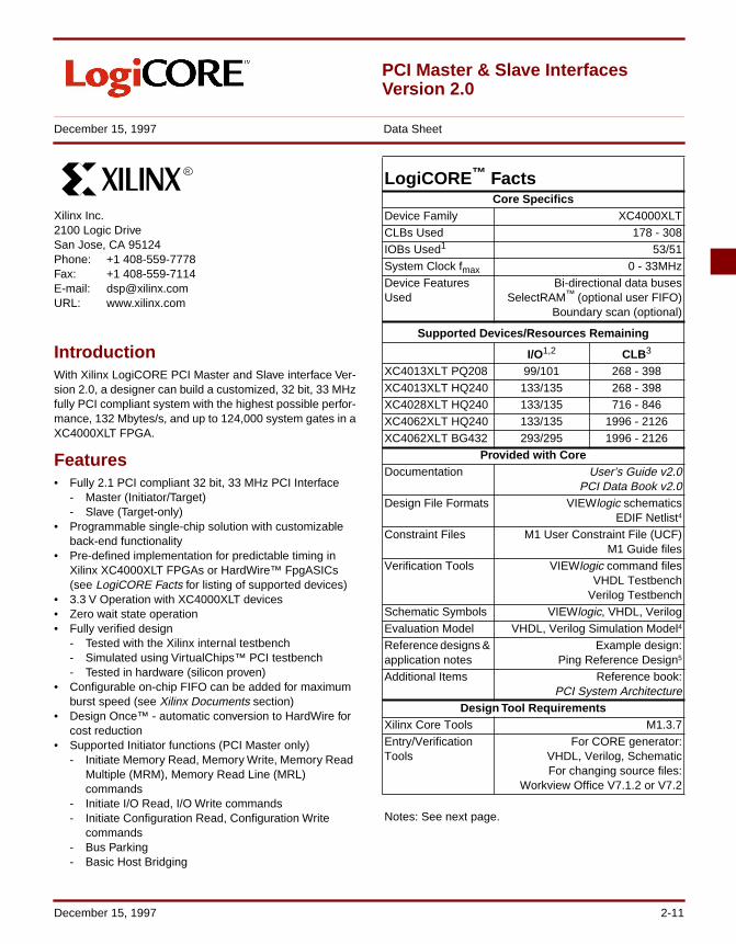
IntroductionWith Xilinx LogiCORE PCI Master and Slave interface Ver-sion 2.0, a designer can build a customized, 32 bit, 33 MHzfully PCI compliant system with the highest possible perfor-mance, 132 Mbytes/s, and up to 124,000 system gates in aXC4000XLT FPGA.
Features• Fully 2.1 PCI compliant 32 bit, 33 MHz PCI Interface
- Master (Initiator/Target)- Slave (Target-only)
• Programmable single-chip solution with customizable back-end functionality
• Pre-defined implementation for predictable timing in Xilinx XC4000XLT FPGAs or HardWire™ FpgASICs (see LogiCORE Facts for listing of supported devices)
• 3.3 V Operation with XC4000XLT devices• Zero wait state operation• Fully verified design
- Tested with the Xilinx internal testbench- Simulated using VirtualChips™ PCI testbench- Tested in hardware (silicon proven)
• Configurable on-chip FIFO can be added for maximum burst speed (see Xilinx Documents section)
• Design Once™ - automatic conversion to HardWire for cost reduction
• Supported Initiator functions (PCI Master only)- Initiate Memory Read, Memory Write, Memory Read
Multiple (MRM), Memory Read Line (MRL) commands
- Initiate I/O Read, I/O Write commands- Initiate Configuration Read, Configuration Write
commands- Bus Parking- Basic Host Bridging
LogiCORE ™ FactsCore Specifics
Device Family XC4000XLTCLBs Used 178 - 308IOBs Used1 53/51System Clock fmax 0 - 33MHzDevice Features Used
Bi-directional data busesSelectRAM™ (optional user FIFO)
Boundary scan (optional)
Supported Devices/Resources Remaining
I/O1,2 CLB3
XC4013XLT PQ208 99/101 268 - 398XC4013XLT HQ240 133/135 268 - 398XC4028XLT HQ240 133/135 716 - 846XC4062XLT HQ240 133/135 1996 - 2126XC4062XLT BG432 293/295 1996 - 2126
Provided with CoreDocumentation User’s Guide v2.0
PCI Data Book v2.0Design File Formats VIEWlogic schematics
EDIF Netlist4
Constraint Files M1 User Constraint File (UCF)M1 Guide files
Verification Tools VIEWlogic command filesVHDL Testbench
Verilog TestbenchSchematic Symbols VIEWlogic, VHDL, VerilogEvaluation Model VHDL, Verilog Simulation Model4
Reference designs & application notes
Example design:Ping Reference Design5
Additional Items Reference book:PCI System Architecture
Design Tool RequirementsXilinx Core Tools M1.3.7Entry/Verification Tools
For CORE generator:VHDL, Verilog, SchematicFor changing source files:
Workview Office V7.1.2 or V7.2
Notes: See next page.
December 15, 1997 2-11

PCI Master & Slave Interfaces Version 2.0PCI Master & Slave Interfaces Version 2.0
Features (cont.)• Supported Target functions (PCI Master and Slave)
- Type 0 Configuration Space Header- Up to 3 Base Address Registers (memory or I/O with
adjustable block size from 16 bytes to 2 Gbytes, slow or medium decode speed)
- Parity Generation (PAR), Parity Error Detection (PERR# and SERR#)
- Memory Read, Memory Write, Memory Read Multiple (MRM), Memory Real Line (MRL), Memory Write, Invalidate (MWI) commands
- I/O Read, I/O Write commands- Configuration Read, Configuration Write commands- 32-bit data transfers, burst transfers with linear
address ordering- Target Abort, Target Retry, Target Disconnect- Full Command/Status Register
• Supported by Xilinx CORE Generator- Web-based configuration- Generation of proven design files
Applications• PCI add-in boards such as graphic cards, video
adapters, LAN adapters and data acquisition boards• Embedded applications within telecommunication and
industrial systems• CompactPCI boards• Other applications that need PCI
General DescriptionThe LogiCORE™ Master and Slave Interfaces v2.0 are pre-implemented and fully tested modules for XilinxXC4000XLT FPGAs (see LogiCORE Facts for listing ofsupported devices). The pin-out and the relative placementof the internal Configurable Logic Blocks (CLBs) are pre-defined. Critical paths are controlled by TimeSpec’s toensure that timing is always met. This significantly reducesengineering time required to implement the PCI portion ofyour design. Resources can instead be focused on the
LogiCORE ™ Facts (cont.)Support
Xilinx provides technical support for this LogiCORE™ product when used as described in the User’s Guide or supporting Application Notes. Xilinx cannot guarantee timing, functionality, or support of the product if imple-mented in devices not listed above, or customized be-yond that referenced in the product documentation, or if any changes are done in sections of the design marked as “DO NOT MODIFY”.Notes:1. Master/Slave2. The XLT devices use 8 I/O locations for Vtt pins3. The exact number of CLBs depends on user configuration of
the core and level of resource sharing with adjacent logic. Fac-tors that can affect the size of the design are number and sizeof the BARs, zero vs. one wait state, and medium vs. slowdecode. These numbers include a 16 x 32 FIFO.
4. Available on Xilinx Home Page, in the LogiCORE PCI VIPLounge: www.xilinx.com/products/logicore/logicore.htm
5. Slave only
ParityGenerator/
Checker
PAR
PERR-
SERR-
PCI Configuration Space
BaseAddressRegister
0
BaseAddressRegister
1
Command/Status
Register
InitiatorState
Machine
InterruptPin and
LineRegister
LatencyTimer
Register
Vendor ID,Rev ID,
Other UserData
X7954
TargetState
Machine
PC
I I/
O I
NT
ER
FA
CE
US
ER
AP
PL
ICA
TIO
N
ADIO[31:0]
AD[31:0]
GNT-
FRAME-
IRDY-
REQ-
TRDY-
DEVSEL-
STOP-
Figure 1: LogiCORE ™ PCI Interface Block Diagram (BAR 2 not shown)
2-12 December 15, 1997
unique back-end logic in the FPGA and the system leveldesign. As a result, the LogiCORE™ PCI products can cutyour development time by several months.
Xilinx XC4000XLT Series FPGAs enables designs of fullyPCI-compliant systems. The devices meet all required elec-trical and timing parameters including AC output drive char-acteristics, input capacitance specifications (10pF), 7 nssetup and 0 ns hold to system clock, and 11 ns systemclock to output. These devices meet all specifications for3.3 V PCI. Although the XLT devices have a 3V driver theycan be used in a 5V PCI system and meet timing for up to8 loads.
The XC4000XLT devices differ from regular XL devices bythe addition of clamp diodes, required by the PCI 3.3 Velectrical specification. For more details about this see theApplication Note, Using the XC4000XL for 3.3 V and 5 VPCI Applications.
The PCI Compliance Checklist (In the PCI Data Book) hasadditional details about electrical compliance. Other fea-tures that enable efficient implementation of a completePCI system in the XC4000XLT includes:
• Select-RAM™ memory: on-chip ultra-fast RAM withsynchronous write option and dual-port RAM option.Used in the PCI Interfaces to implement the FIFO.
• Individual output enable for each I/O• Internal 3-state bus capability• 8 global low-skew clock or signal distribution networks• IEEE 1149.1-compatible boundary scan logic support
See the latest Xilinx Programmable Logic Data Book formore details.
The module is carefully optimized for best possible perfor-mance and utilization in the XC4000XLT FPGA architec-ture. When implemented in the XC4013, more than 50% ofthe FPGA’s resources remain for integrating a unique back-end interface and other system functions into a fully pro-grammable one-chip solution. When implemented in aXC4062, 90% of the FPGA’s resources remain.
Xilinx DesignOnce™ service allows an automatic conver-sion to a low cost HardWire™ device for high-volume pro-duction.
Functional DescriptionThe LogiCORE PCI Master Interface is partitioned into fivemajor blocks, plus the user application, shown in Figure 1.Each block is described below.
PCI I/O Interface BlockThe I/O interface block handles the physical connection tothe PCI bus including all signaling, input and output syn-chronization, output three-state controls, and all request-grant handshaking for bus mastering.
Parity Generator/CheckerGenerates/checks even parity across the AD bus, the CBElines, and the PAR signal. Reports data parity errors viaPERR- and address parity errors via SERR-.
Target State MachineThis block manages control over the PCI interface for Tar-get functions. The states implemented are a subset ofequations defined in “Appendix B” of the PCI Local BusSpecification. The controller is a high-performance statemachine using state-per-bit (one-hot) encoding for maxi-mum performance. State-per-bit encoding has narrowerand shallower next-state logic functions that closely matchthe Xilinx FPGA architecture.
Initiator State Machine (PCI Master only)This block manages control over the PCI interface for Initia-tor functions. The states implemented are a subset of equa-tions defined in “Appendix B” of the PCI Local BusSpecification. The Initiator Control Logic also uses state-per-bit encoding for maximum performance.
PCI Configuration SpaceThis block provides the first 64 bytes of Type 0, version 2.1,Configuration Space Header (CSH) (see Table 1) to sup-port software-driven “Plug-and Play” initialization and con-figuration. This includes Command, Status, and three BaseAddress Registers (BARs). BAR 2 is not shown in figure 1.These BARs illustrate how to implement memory- or I/O-mapped address spaces. Each BAR sets the base addressfor the interface and allows the system software to deter-mine the addressable range required by the interface.Using a combination of Configurable Logic Block (CLB) flip-flops for the read/write registers and CLB look-up tables forthe read-only registers results in optimized packing densityand layout.
With this release, the hooks for extending configurationspace has been built into the backend interface. Thesehooks, including the ability to implement a CapPtr in config-uration space, allows the user to implement functions suchas Advanced Configuration and Power Interface (ACPI) inthe backend design.
December 15, 1997 2-13
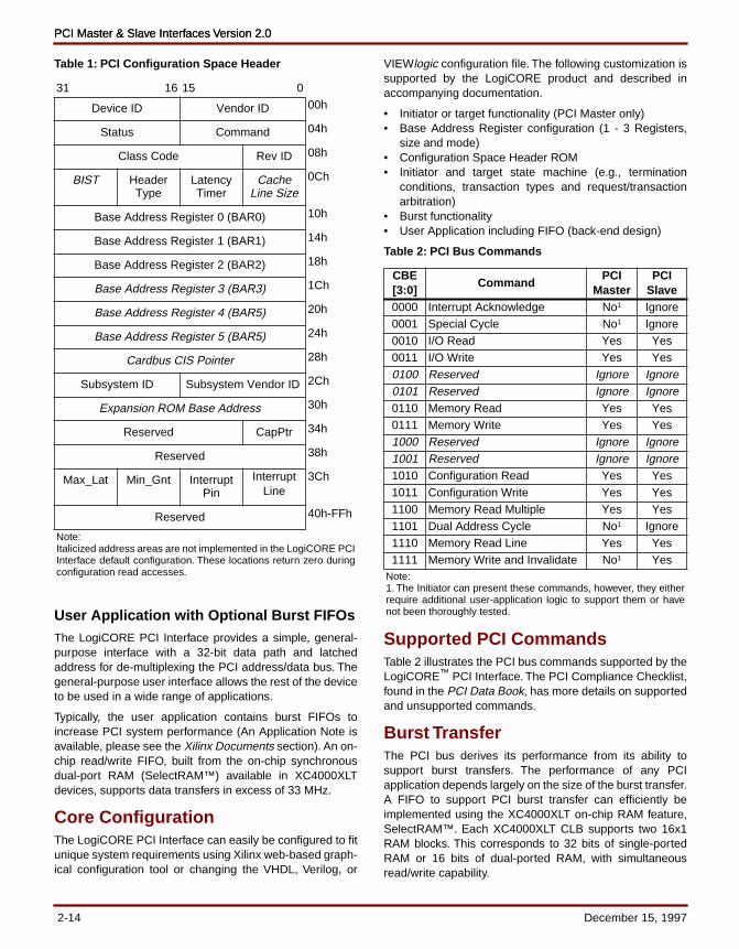
PCI Master & Slave Interfaces Version 2.0PCI Master & Slave Interfaces Version 2.0
Table 1: PCI Configuration Space Header
User Application with Optional Burst FIFOsThe LogiCORE PCI Interface provides a simple, general-purpose interface with a 32-bit data path and latchedaddress for de-multiplexing the PCI address/data bus. Thegeneral-purpose user interface allows the rest of the deviceto be used in a wide range of applications.
Typically, the user application contains burst FIFOs toincrease PCI system performance (An Application Note isavailable, please see the Xilinx Documents section). An on-chip read/write FIFO, built from the on-chip synchronousdual-port RAM (SelectRAM™) available in XC4000XLTdevices, supports data transfers in excess of 33 MHz.
Core ConfigurationThe LogiCORE PCI Interface can easily be configured to fitunique system requirements using Xilinx web-based graph-ical configuration tool or changing the VHDL, Verilog, or
VIEWlogic configuration file. The following customization issupported by the LogiCORE product and described inaccompanying documentation.
• Initiator or target functionality (PCI Master only)• Base Address Register configuration (1 - 3 Registers,
size and mode)• Configuration Space Header ROM• Initiator and target state machine (e.g., termination
conditions, transaction types and request/transactionarbitration)
• Burst functionality• User Application including FIFO (back-end design)
Table 2: PCI Bus Commands
Supported PCI CommandsTable 2 illustrates the PCI bus commands supported by theLogiCORE™ PCI Interface. The PCI Compliance Checklist,found in the PCI Data Book, has more details on supportedand unsupported commands.
Burst TransferThe PCI bus derives its performance from its ability tosupport burst transfers. The performance of any PCIapplication depends largely on the size of the burst transfer.A FIFO to support PCI burst transfer can efficiently beimplemented using the XC4000XLT on-chip RAM feature,SelectRAM™. Each XC4000XLT CLB supports two 16x1RAM blocks. This corresponds to 32 bits of single-portedRAM or 16 bits of dual-ported RAM, with simultaneousread/write capability.
31 16 15 0
Device ID Vendor ID 00h
Status Command 04h
Class Code Rev ID 08h
BIST Header Type
Latency Timer
Cache Line Size
0Ch
Base Address Register 0 (BAR0) 10h
Base Address Register 1 (BAR1) 14h
Base Address Register 2 (BAR2) 18h
Base Address Register 3 (BAR3) 1Ch
Base Address Register 4 (BAR5) 20h
Base Address Register 5 (BAR5) 24h
Cardbus CIS Pointer 28h
Subsystem ID Subsystem Vendor ID 2Ch
Expansion ROM Base Address 30h
Reserved CapPtr 34h
Reserved 38h
Max_Lat Min_Gnt Interrupt Pin
Interrupt Line
3Ch
Reserved 40h-FFh
Note: Italicized address areas are not implemented in the LogiCORE PCIInterface default configuration. These locations return zero duringconfiguration read accesses.
CBE[3:0]
CommandPCI
MasterPCI
Slave0000 Interrupt Acknowledge No1 Ignore0001 Special Cycle No1 Ignore0010 I/O Read Yes Yes0011 I/O Write Yes Yes0100 Reserved Ignore Ignore0101 Reserved Ignore Ignore0110 Memory Read Yes Yes0111 Memory Write Yes Yes1000 Reserved Ignore Ignore1001 Reserved Ignore Ignore1010 Configuration Read Yes Yes1011 Configuration Write Yes Yes1100 Memory Read Multiple Yes Yes1101 Dual Address Cycle No1 Ignore1110 Memory Read Line Yes Yes1111 Memory Write and Invalidate No1 Yes
Note:1. The Initiator can present these commands, however, they eitherrequire additional user-application logic to support them or havenot been thoroughly tested.
2-14 December 15, 1997
Wait StatesIn this version of the core, the wait state is switch select-able. The XC4013XLT-1 is able to run without wait states.The XC4028XLT-1 and the XC4062XLT-1 will require onewait state. Faster speed grades will allow zero wait stateoperation.
In the Zero Wait state mode, no wait states are insertedeither while sourcing data or receiving data. This allows a100% burst transfer rate in both directions with full PCIcompliance. No additional wait states are inserted inresponse to a wait state from another agent on the bus.Either IRDY or TRDY is kept asserted until the current dataphase ends.
In one wait state mode, the LogiCORE Interface automati-cally inserts a wait state when sourcing data (Initiator Write,Target Read) during a burst transfer. In this mode, the Log-iCORE Interface can accept data at 100% burst transferrate and supply data at 50%.
See Table 3 for a PCI bus transfer rates for various opera-tions in either zero or one wait state mode.
Table 3: LogiCORE PCI Transfer Rates
Timing SpecificationThe XC4000XLT family, together with the LogiCORE PCIproducts enables design of fully compliant PCI systems.Backend design can affect the maximum speed yourdesign is capable of. Factors in your back-end designs thatcan affect timing include loading of hot signals comingdirectly from the PCI bus, and gate count. Table 4 showsthe key timing parameters for the LogiCORE PCI Interfacesthat must be met for full PCI compliance.
Verification MethodsXilinx has developed an internal testbench with numerousvectors to test the Xilinx PCI design. The LogiCORE PCIInterfaces have also been extensively simulated using the
VirtualChips VHDL PCI test bench from Phoenix Technolo-gies, Ltd. (not included with the LogiCORE PCI products).The Interface has also been verified in hardware in theXC4013XLT-1 PQ208C FPGA.
Included with the LogiCORE PCI Master and Slave Inter-face is an example design and a VIEWlogic based PCI pro-tocol test bench that verifies the PCI interface functionsaccording to the test scenarios specified in the PCI LocalBus Specification see Figure 2. This test bench consists of28 test scenarios, each designed to test compliance to aspecific PCI bus operation. Refer to the checklist in the PCIData Book for a complete list of test scenarios.
Table 4: Timing Parameters [ns]
Ping Reference DesignThe Xilinx LogiCORE™ PCI “PING” Application Example,delivered in VHDL and Verilog, has been developed to pro-vide an easy-to-understand example which demonstratesmany of the principles and techniques required to success-fully use the LogiCORE™ PCI macro in a System On AChip solution.
Zero Wait State ModeOperation Transfer Rate
Initiator Write (PCI ← LogiCORE) 3-1-1-2Initiator Read (PCI → LogiCORE) 4-1-1-2Target Write (PCI→ LogiCORE) 5-1-1-1Target Read (PCI ← LogiCORE) 6-1-1-1
One Wait State ModeOperation Transfer Rate
Initiator Write (PCI ← LogiCORE) 3-2-2-2Initiator Read (PCI → LogiCORE) 4-1-1-2Target Write (PCI→ LogiCORE) 5-1-1-1Target Read (PCI ← LogiCORE) 6-2-2-2Note:Initiator Read and Target Write operations have effectively thesame bandwidth for burst transfer.
Parameter Ref. PCI Spec.
LogiCORE PCI,
XC4000XLT-1Min Max Min Max
CLK Cycle Time 30 ∞ 301 ∞CLK High Time 11 11CLK Low Time 11 11CLK to Bus Sig-nals Valid3
TICK-
OF
2 11 22 8.5
CLK to REQ# and GNT# Valid3
TICK-
OF
2 12 22 8.5
Tri-state to Active 2 22
CLK to Tri-state 28 281
Bus Signal Setup to CLK (IOB)
TPSD 7 7
Bus Signal Setup to CLK (CLB)
7 71
GNT# Setup to CLK
TPSD 10 7
Input Hold Time After CLK (IOB)
TPHD 0 0
Input Hold Time After CLK (CLB)
0 02
RST# to Tri-state 40 402
Notes:1. Controlled by TIMESPECS, included in product2. Verified by analysis and bench-testing3. IOB configured for Fast slew rate
December 15, 1997 2-15
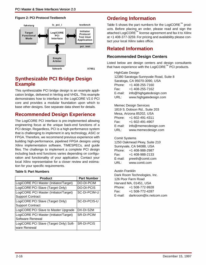
PCI Master & Slave Interfaces Version 2.0PCI Master & Slave Interfaces Version 2.0
Figure 2: PCI Protocol Testbench
Synthesizable PCI Bridge Design ExampleThis synthesizable PCI bridge design is an example appli-cation bridge, delivered in Verilog and VHDL. This exampledemonstrates how to interface to the LogiCORE V2.0 PCIcore and provides a modular foundation upon which tobase other designs. See separate data sheet for details.
Recommended Design ExperienceThe LogiCORE PCI interface is pre-implemented allowingengineering focus at the unique back-end functions of aPCI design. Regardless, PCI is a high-performance systemthat is challenging to implement in any technology, ASIC orFPGA. Therefore, we recommend previous experience withbuilding high-performance, pipelined FPGA designs usingXilinx implementation software, TIMESPECs, and guidefiles. The challenge to implement a complete PCI designincluding back-end functions varies depending on configu-ration and functionality of your application. Contact yourlocal Xilinx representative for a closer review and estima-tion for your specific requirements.
Table 5: Part Numbers
Ordering InformationTable 5 shows the part numbers for the LogiCORE™ prod-ucts. Before placing an order, please read and sign theattached LogiCORE™ license agreement and fax it to Xilinxat +1 408-377-3259. For pricing and availability please con-tact your local Xilinx sales office.
Related Information
Recommended Design CentersListed below are design centers and design consultantsthat have experience with the LogiCORE™ PCI products.
HighGate Design12380 Saratoga-Sunnyvale Road, Suite 8Saratoga, CA 95070-3090, USAPhone: +1 408-255-7160Fax: +1 408-255-7162E-mail: [email protected]: www.highgatedesign.com
Memec Design Services1819 S. Dobson Rd., Suite 203Mesa, Arizona 85202, USAPhone: +1 602-491-4311Fax: +1 602-491-4907E-mail: [email protected]: www.memecdesign.com
Comit Systems1250 Oakmead Pkwy, Suite 210Sunnyvale, CA 94088, USAPhone: +1 408-988-2987Fax: +1 408-988-2133E-mail: [email protected]: www.comit.com
Austin FranklinDark Room Technologies, Inc.126 Poor Farm RoadHarvard MA, 01451, USAPhone: +1 508-772-9928Fax: +1 508-772-4287E-mail: [email protected]
Product Part NumberLogiCORE PCI Master (Initiator/Target) DO-DI-PCIMLogiCORE PCI Slave (Target Only) DO-DI-PCISLogiCORE PCI Master (Initiator/Target) Support Contract
SC-DI-PCIM-U
LogiCORE PCI Slave (Target Only)Support Contract
SC-DI-PCIS-U
LogiCORE PCI Slave to Master Upgrade DX-DI-S2MLogiCORE PCI Master (Initiator/Target) Software Renewal
SR-DI-PCIM
LogiCORE PCI Slave (Target Only) Soft-ware Renewal
SR-DI-PCIS
LogiCOREPCI
Interface
SimpleArbiter
fakearb
lc_pci_i
TargetFunctional
Mode
faketarg testbnch
pci_test
InitiatorProtocolTest User
Application
X7951
2-16 December 15, 1997
PCI Special Interest Group (PCI-SIG) PublicationsThe PCI-SIG publishes various PCI specifications andrelated documents such as PCI Local Bus Specification,PCI Compliance Checklist and PCI System Design Guide.
PCI Special Interest Group2575 NE Kathryn St. #17Hillsboro, OR 97124Phone: +1 800-433-5177 (inside the US)
+1 503-693-6232 (outside the US)Fax: +1 503-693-8344Office hours: 8:30am - 4:00pm PSTE-mail: [email protected]: www.pcisig.com
Xilinx DocumentsMore PCI related information is available on Xilinx Web:
www.xilinx.com/products/logicore/logicore.htm.
December 15, 1997 2-17
PCI Master & Slave Interfaces Version 2.0PCI Master & Slave Interfaces Version 2.0
Name:
(Signed) (Date)
Printed:
Title: Company:
Address:
E-mail: PO#:
Fax to: +1 408-377-3259 (USA)
PLEASE READ THIS DOCUMENT CAREFULLY BEFORE USING THE XIL-INX LOGICORE PCI MASTER INTERFACE OR PCI SLAVE INTERFACEDESIGN, BY USING THE XILINX LOGICORE DESIGN, YOU ARE AGREE-ING TO BE BOUND BY THE TERMS OF THIS LICENSE.
1. License. XILINX, INC. (“XILINX”) hereby grants you a nonexclusive, non-transferable license to use the LOGICORE PCI MASTER/SLAVE INTER-FACEdesign (the “Design”), solely for your use in developing designs forXILINX programmable logic devices or XILINX HardWire™ devices. Useof the Design in non-XILINX devices or technologies is prohibited unlessyou have entered into a separate written agreement with XILINX for suchuse. XILINX retains title to the Design and to any patents, copyrights, tradesecrets and other intellectual property rights therein. To protect such intel-lectual property rights, you may not decompile, reverse engineer, disas-semble, or otherwise reduce the Design to a human-perceivable form. Youmay not modify or prepare derivative works of the Design in whole or inpart. This License allows you to make an unlimited number of copies of theDesign for internal use only, provided you reproduce on each copy of theDesign the copyright and any other proprietary legends that were on theoriginal copy of the Design.
2. Termination. This License is effective until terminated. You may terminatethis License at any time by destroying the Design and all copies thereof.This License will terminate immediately without notice from XILINX if youfail to comply with any provision of this License. Upon termination youmust destroy the Design and all copies thereof.
3. Governmental Use. The Design is commercial computer software devel-oped exclusively at Xilinx’s expense. Accordingly, pursuant to the FederalAcquisition Regulations (FAR) Section 12.212 and Defense FAR Supple-ment Section 227.2702, use, duplication and disclosure of the Design byor for the Government is subject to the restrictions set forth in this LicenseAgreement. Manufacturer is XILINX, INC., 2100 Logic Drive, San Jose,California 95124.
4. Limited Warranty and Disclaimer. THE DESIGN IS PROVIDED TO YOU“AS IS”. XILINX AND ITS LICENSORS MAKE AND YOU RECEIVE NOWARRANTIES OR CONDITIONS, EXPRESS, IMPLIED, STATUTORYOR OTHERWISE, AND XILINX SPECIFICALLY DISCLAIMS ANYIMPLIED WARRANTIES OF MERCHANTABILITY, NON-INFRINGE-MENT, OR FITNESS FOR A PARTICULAR PURPOSE. XILINX does notwarrant that the functions contained in the Design will meet your require-ments, or that the operation of the Design will be uninterrupted or errorfree, or that defects in the Design will be corrected. Furthermore, XILINX
does not warrant or make any representations regarding use or the resultsDesign in terms of correctness, accuracy, reliability or otherwise.
5. Limitation of Liability. IN NO EVENT WILL XILINX OR ITS LICENSORSBE LIABLE FOR ANY LOSS OF DATA, LOST PROFITS, COST OF PRO-CUREMENT OF SUBSTITUTE GOODS OR SERVICES, OR FOR ANYSPECIAL, INCIDENTAL, CONSEQUENTIAL OR INDIRECT DAMAGESARISING FROM THE USE OR OPERATION OF THE DESIGN ORACCOMPANYING DOCUMENTATION, HOWEVER CAUSED AND ONANY THEORY OF LIABILITY. THIS LIMITATIN WILL APPLY EVEN IF XIL-INX HAS BEEN ADVISED OF THE POSSIBILITY OF SUCH DAMAGE.THIS LIMITATION SHALL APPLY NOTWITHSTANDING THE FAILUREOF THE ESSENTIAL PURPOSE OF ANY LIMITED REMEDIES HEREIN.
6. Export Restriction. You agree that you will not export or re-export theDesign, reference images or accompanying documentation in any formwithout the appropriate United States and foreign government licenses.Your failure to comply with this provision is a material breach of this Agree-ment.
7. Third Party Beneficiary. You understand that portions of the Design andrelated documentation may have been licensed to XILINX from third par-ties and that such third parties are intended third party beneficiaries of theprovisions of this Agreement.
8. Non-Transferable. You may not provide design source information includ-ing, but not limited to, schematics, hardware description language sourcecode, or netlist files, to a third party without prior written approval from XIL-INX. You may provide device programming files— XILINX bit-stream filesor PROM files—of the resulting HardWire gate array to third-parties with-out prior approval.
9. General. This License shall be governed by the laws of the State of Cali-fornia, without reference to conflict of laws principles. If for any reason acourt of competent jurisdiction finds any provision of this License, or por-tion thereof, to be unenforceable, that provision of this License shall bereplaced to the maximum extent permissible so as to effectuate the intentof the parties, and the remainder of this License shall continue in full forceand effect. This License constitutes the entire agreement between the par-ties with respect to the use of this Design and related documentation, andsupersedes all prior or contemporaneous understandings or agreement,written or oral, regarding such subject matter.
I have read the Xilinx LogiCORE License Agreement, and I agreement to com-ply with the terms and conditions therein.
XILINX LOGICORE™ “PCI MASTER INTERFACE” AND “PCI SLAVE INTERFACE” LICENSE
AGREEMENT
2-18 December 15, 1997
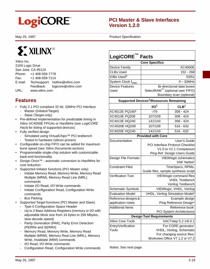
PCI Master & Slave Interfaces Version 1.2.0
May 25, 1997 Product Specification
Xilinx Inc.2100 Logic DriveSan Jose, CA 95124Phone: +1 408-559-7778Fax: +1 408-559-7114E-mail: Techsupport: [email protected]
Feedback: [email protected]: www.xilinx.com
R
Features• Fully 2.1 PCI compliant 32 bit, 33MHz PCI Interface
- Master (Initiator/Target)- Slave (Target-only)
• Pre-defined implementation for predictable timing in Xilinx XC4000E FPGAs or HardWire (see LogiCORE Facts for listing of supported devices)
• Fully verified design- Simulated using VirtualChips™ PCI testbench- Tested in hardware (silicon proven)
• Configurable on-chip FIFO can be added for maximum burst speed (see Xilinx Documents section)
• Programmable single-chip solution with customizable back-end functionality
• Design Once™ - automatic conversion to HardWire for cost reduction
• Supported Initiator functions (PCI Master only)- Initiate Memory Read, Memory Write, Memory Read
Multiple (MRM), Memory Read Line (MRL) commands
- Initiate I/O Read, I/O Write commands- Initiate Configuration Read, Configuration Write
commands- Bus Parking
• Supported Target functions (PCI Master and Slave)- Type 0 Configuration Space Header- Up to 2 Base Address Registers (memory or I/O with
adjustable block size from 16 bytes to 256 Mbytes, slow decode speed)
- Parity Generation (PAR), Parity Error Detection (PERR# and SERR#)
- Memory Read, Memory Write, Memory Read Multiple (MRM), Memory Real Line (MRL), Memory Write, Invalidate (MWI) commands
- I/O Read, I/O Write commands- Configuration Read, Configuration Write commands
LogiCORE ™ FactsCore Specifics
Device Family XC4000ECLBs Used 152 - 268IOBs Used5 53/51System Clock fmax 0 − 33MHzDevice Features Used
Bi-directional data busesSelectRAM™ (optional user FIFO)
Boundary scan (optional)
Supported Devices 1/Resources Remaining
I/O5 CLB2
XC4013E PQ1606 -/76 308 - 424XC4013E PQ208 107/109 308 - 424XC4013E HQ240 141/143 308 - 424
XC4020E HQ208 107/109 516 - 632
XC4020E HQ240 141/143 516 - 632Provided with Core
Documentation User’s GuidePCI Interface Protocol Checklist
V1.0 to V1.1 ComparisonPing Ref. Design Users Guide
Design File Formats VIEWlogic schematicsXNF Netlist3
Constraint Files TimeSpecs, RPMs,Guide files, sample synthesis script
Verification Tool VIEWlogic command filesVHDL Testbench
Verilog TestbenchSchematic Symbols VIEWlogic, VHDL, VerilogEvaluation Model VHDL, Verilog Simulation Model3
Reference designs & application notes
Example designPing Reference Design4
Additional Items Reference book:PCI System Architectures
Design Tool RequirementsXilinx Core Tools XACTstep 5.2.1/6.0.1Entry/Verification Tools
For CORE generator:VHDL, Verilog, SchematicFor changing source files:
Workview Office V7.1.2 or V7.2
Notes: See next page.
May 25, 1997 2-19
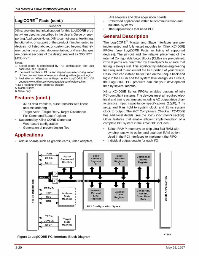
PCI Master & Slave Interfaces Version 1.2.0PCI Master & Slave Interfaces Version 1.2.0
Features (cont.)- 32-bit data transfers, burst transfers with linear
address ordering- Target Abort, Target Retry, Target Disconnect- Full Command/Status Register
• Supported by Xilinx CORE Generator- Web-based configuration- Generation of proven design files
Applications• Add-in boards such as graphic cards, video adapters,
LAN adapters and data acquisition boards.• Embedded applications within telecommunication and
industrial systems.• Other applications that need PCI
General DescriptionThe LogiCORE™ Master and Slave Interfaces are pre-implemented and fully tested modules for Xilinx XC4000EFPGAs (see LogiCORE Facts for listing of supporteddevices). The pin-out and the relative placement of theinternal Configurable Logic Blocks (CLBs) are pre-defined.Critical paths are controlled by TimeSpec’s to ensure thattiming is always met. This significantly reduces engineeringtime required to implement the PCI portion of your design.Resources can instead be focused on the unique back-endlogic in the FPGA and the system level design. As a result,the LogiCORE PCI products can cut your developmenttime by several months.
Xilinx XC4000E Series FPGAs enables designs of fullyPCI-compliant systems. The devices meet all required elec-trical and timing parameters including AC output drive char-acteristics, input capacitance specifications (10pF), 7 nssetup and 0 ns hold to system clock, and 11 ns systemclock to output. The PCI Compliance Checklist XC4000Ehas additional details (see the Xilinx Documents section).Other features that enable efficient implementation of acomplete PCI system in the XC4000E includes:
• Select-RAM™ memory: on-chip ultra-fast RAM with synchronous write option and dual-port RAM option. Used in the PCI Interfaces to implement the FIFO.
• Individual output enable for each I/O
LogiCORE ™ Facts (cont.)Support
Xilinx provides technical support for this LogiCORE prod-uct when used as described in the User’s Guide or sup-porting Application Notes. Xilinx cannot guarantee timing, functionality, or support of the product if implemented in devices not listed above, or customized beyond that ref-erenced in the product documentation, or if any changes are done in sections of the design marked as “DO NOT MODIFY”.Notes:1. Speed grade is determined by PCI configuration and user
back-end, see Figure 3. 2. The exact number of CLBs and depends on user configuration
of the core and level of resource sharing with adjacent logic.3. Available on Xilinx Home Page, in the LogiCORE PCI VIP
Lounge: www.xilinx.com/products/logicore/logicore.htm4. See heading “Ping Reference Design”5. Master/Slave6. Slave only
ParityGenerator/
Checker
PAR
PERR-
SERR-
PCI Configuration Space
BaseAddressRegister
0
BaseAddressRegister
1
Command/Status
Register
InitiatorState
Machine
InterruptPin and
LineRegister
LatencyTimer
Register
Vendor ID,Rev ID,
Other UserData
X7954
TargetState
Machine
PC
I I/
O I
NT
ER
FA
CE
US
ER
AP
PL
ICA
TIO
N
ADIO[31:0]
AD[31:0]
GNT-
FRAME-
IRDY-
REQ-
TRDY-
DEVSEL-
STOP-
Figure 1: LogiCORE PCI Interface Block Diagram
2-20 May 25, 1997

• Internal 3-state bus capability• 8 global low-skew clock or signal distribution networks• IEEE 1149.1-compatible boundary scan logic support
See Xilinx 1996 Data Book for more details.
The module is carefully optimized for best possible perfor-mance and utilization in the XC4000E FPGA architecture.Implemented in the smallest supported FPGA, XC4013,more than 50% of the FPGA’s resources remain for inte-grating a unique back-end interface and other system func-tions into a fully programmable one-chip solution.
Xilinx DesignOnceTM service allows an automatic conver-sion to a low cost HardWire™ device for high-volume pro-duction.
Functional DescriptionThe LogiCORE PCI Master Interface is partitioned into fivemajor blocks, plus the user application, shown in Figure 1.Each block is described below.
PCI I/O Interface BlockThe I/O interface block handles the physical connection tothe PCI bus including all signaling, input and output syn-chronization, output three-state controls, and all request-grant handshaking for bus mastering.
Parity Generator/CheckerGenerates/checks even parity across the AD bus, the CBElines, and the PAR signal. Reports data parity errors viaPERR- and address parity errors via SERR-.
Target State MachineThis block manages control over the PCI interface for Tar-get functions. The states implemented are a subset ofequations defined in “Appendix B” of the PCI Local BusSpecification. The controller is a high-performance statemachine using state-per-bit (one-hot) encoding for maxi-mum performance. State-per-bit encoding has narrowerand shallower next-state logic functions that closely matchthe Xilinx FPGA architecture.
Initiator State Machine (PCI Master only)This block manages control over the PCI interface for Initia-tor functions. The states implemented are a subset of equa-tions defined in “Appendix B” of the PCI Local BusSpecification. The Initiator Control Logic also uses state-per-bit encoding for maximum performance.
PCI Configuration SpaceThis block provides the first 64 bytes of Type 0, version 2.1,Configuration Space Header (CSH) (see Table 1) to sup-port software-driven “Plug-and Play” initialization and con-figuration. This includes Command, Status, and two BaseAddress Registers (BARs). These BARs illustrate how to
implement memory- or I/O-mapped address spaces. EachBAR sets the base address for the interface and allows thesystem software to determine the addressable rangerequired by the interface. Using a combination of Config-urable Logic Block (CLB) flip-flops for the read/write regis-ters and CLB look-up tables for the read-only registersresults in optimized packing density and layout.
Table 1: PCI Configuration Space Header
User Application with Optional Burst FIFOsThe LogiCORE PCI Interface provides a simple, general-purpose interface with a 32-bit data path and latchedaddress for de-multiplexing the PCI address/data bus. Thegeneral-purpose user interface allows the rest of the deviceto be used in a wide range of applications.
Typically, the user application contains burst FIFOs toincrease PCI system performance (An Application Note isavailable, please see the Xilinx Documents section). An on-chip read/write FIFO, built from the on-chip synchronous
31 16 15 0
Device ID Vendor ID 00h
Status Command 04h
Class Code Rev ID 08h
BIST Header Type
Latency Timer
Cache Line Size
0Ch
Base Address Register 0 (BAR0) 10h
Base Address Register 1 (BAR1) 14h
Base Address Register 2 (BAR2) 18h
Base Address Register 3 (BAR3) 1Ch
Base Address Register 4 (BAR5) 20h
Base Address Register 5 (BAR5) 24h
Cardbus CIS Pointer 28h
Subsystem ID Subsystem Vendor ID
2Ch
Expansion ROM Base Address 30h
Reserved 34h
Reserved 38h
Max_Lat Min_Gnt Interrupt Pin
Interrupt Line
3Ch
Note: Italicized address areas are not implemented in the LogiCORE PCIInterface default configuration. These locations return zero duringconfiguration read accesses.
May 25, 1997 2-21
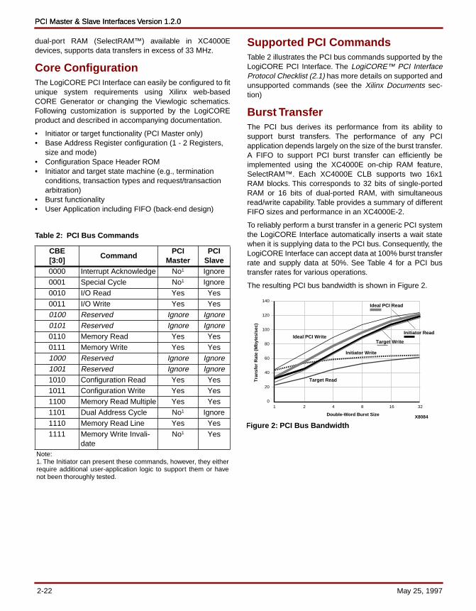
PCI Master & Slave Interfaces Version 1.2.0PCI Master & Slave Interfaces Version 1.2.0
dual-port RAM (SelectRAM™) available in XC4000Edevices, supports data transfers in excess of 33 MHz.
Core ConfigurationThe LogiCORE PCI Interface can easily be configured to fitunique system requirements using Xilinx web-basedCORE Generator or changing the Viewlogic schematics.Following customization is supported by the LogiCOREproduct and described in accompanying documentation.
• Initiator or target functionality (PCI Master only)• Base Address Register configuration (1 - 2 Registers,
size and mode)• Configuration Space Header ROM• Initiator and target state machine (e.g., termination
conditions, transaction types and request/transaction arbitration)
• Burst functionality• User Application including FIFO (back-end design)
Table 2: PCI Bus Commands
Supported PCI CommandsTable 2 illustrates the PCI bus commands supported by theLogiCORE PCI Interface. The LogiCORE™ PCI InterfaceProtocol Checklist (2.1) has more details on supported andunsupported commands (see the Xilinx Documents sec-tion)
Burst TransferThe PCI bus derives its performance from its ability tosupport burst transfers. The performance of any PCIapplication depends largely on the size of the burst transfer.A FIFO to support PCI burst transfer can efficiently beimplemented using the XC4000E on-chip RAM feature,SelectRAM™. Each XC4000E CLB supports two 16x1RAM blocks. This corresponds to 32 bits of single-portedRAM or 16 bits of dual-ported RAM, with simultaneousread/write capability. Table provides a summary of differentFIFO sizes and performance in an XC4000E-2.
To reliably perform a burst transfer in a generic PCI systemthe LogiCORE Interface automatically inserts a wait statewhen it is supplying data to the PCI bus. Consequently, theLogiCORE Interface can accept data at 100% burst transferrate and supply data at 50%. See Table 4 for a PCI bustransfer rates for various operations.
The resulting PCI bus bandwidth is shown in Figure 2.
CBE[3:0]
CommandPCI
MasterPCI
Slave0000 Interrupt Acknowledge No1 Ignore0001 Special Cycle No1 Ignore0010 I/O Read Yes Yes0011 I/O Write Yes Yes0100 Reserved Ignore Ignore0101 Reserved Ignore Ignore0110 Memory Read Yes Yes0111 Memory Write Yes Yes1000 Reserved Ignore Ignore1001 Reserved Ignore Ignore1010 Configuration Read Yes Yes1011 Configuration Write Yes Yes1100 Memory Read Multiple Yes Yes1101 Dual Address Cycle No1 Ignore1110 Memory Read Line Yes Yes1111 Memory Write Invali-
dateNo1 Yes
Note:1. The Initiator can present these commands, however, they eitherrequire additional user-application logic to support them or havenot been thoroughly tested.
X8084Double-Word Burst Size
Tra
nsf
er R
ate
(Mb
ytes
/sec
)
01 2 4 8 16 32
20
40
60
80
100
120
140
Ideal PCI Write
Ideal PCI Read
Initiator Read
Target Write
Initiator Write
Target Read
Figure 2: PCI Bus Bandwidth
2-22 May 25, 1997
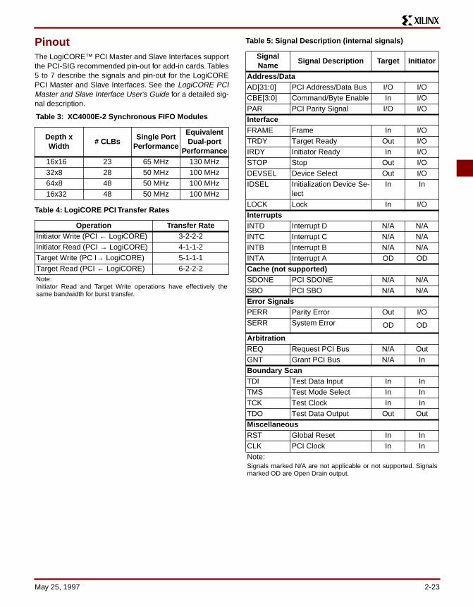
PinoutThe LogiCORE™ PCI Master and Slave Interfaces supportthe PCI-SIG recommended pin-out for add-in cards. Tables5 to 7 describe the signals and pin-out for the LogiCOREPCI Master and Slave Interfaces. See the LogiCORE PCIMaster and Slave Interface User’s Guide for a detailed sig-nal description.
Table 3: XC4000E-2 Synchronous FIFO Modules
Table 4: LogiCORE PCI Transfer Rates
Table 5: Signal Description (internal signals)
Depth x Width
# CLBsSingle Port
Performance
Equivalent Dual-port
Performance16x16 23 65 MHz 130 MHz32x8 28 50 MHz 100 MHz64x8 48 50 MHz 100 MHz16x32 48 50 MHz 100 MHz
Operation Transfer RateInitiator Write (PCI ← LogiCORE) 3-2-2-2Initiator Read (PCI → LogiCORE) 4-1-1-2Target Write (PC I→ LogiCORE) 5-1-1-1Target Read (PCI ← LogiCORE) 6-2-2-2Note:Initiator Read and Target Write operations have effectively thesame bandwidth for burst transfer.
Signal Name
Signal Description Target Initiator
Address/DataAD[31:0] PCI Address/Data Bus I/O I/OCBE[3:0] Command/Byte Enable In I/OPAR PCI Parity Signal I/O I/OInterfaceFRAME Frame In I/OTRDY Target Ready Out I/OIRDY Initiator Ready In I/OSTOP Stop Out I/ODEVSEL Device Select Out I/OIDSEL Initialization Device Se-
lectIn In
LOCK Lock In I/OInterruptsINTD Interrupt D N/A N/AINTC Interrupt C N/A N/AINTB Interrupt B N/A N/AINTA Interrupt A OD ODCache (not supported)SDONE PCI SDONE N/A N/ASBO PCI SBO N/A N/AError SignalsPERR Parity Error Out I/OSERR System Error OD OD
ArbitrationREQ Request PCI Bus N/A OutGNT Grant PCI Bus N/A InBoundary ScanTDI Test Data Input In InTMS Test Mode Select In InTCK Test Clock In InTDO Test Data Output Out OutMiscellaneousRST Global Reset In InCLK PCI Clock In InNote: Signals marked N/A are not applicable or not supported. Signalsmarked OD are Open Drain output.
May 25, 1997 2-23
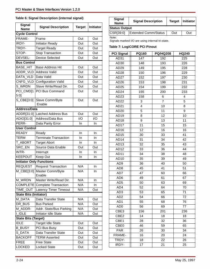
PCI Master & Slave Interfaces Version 1.2.0PCI Master & Slave Interfaces Version 1.2.0
Table 6: Signal Description (internal signal)
Table 7: LogiCORE PCI Pinout
Signal Name
Signal Description Target Initiator
Cycle ControlFRAME- Frame Out OutIRDY- Initiator Ready Out OutTRDY- Target Ready Out OutSTOP- Stop Transaction Out OutDEVSEL- Device Selected Out OutBus ControlBASE_HIT Base Address Hit Out OutADDR_VLD Address Valid Out OutDATA_VLD Data Valid Out OutCNFG_VLD Configuration Valid Out OutS_WRDN Slave Write/Read Dir. Out OutPCI_CMD[15:0]
PCI Bus Command Out Out
S_CBE[3:0] Slave Comm/Byte Enable
Out Out
Address/DataADDR[31:0] Latched Address Bus Out OutADIO[31:0] Address/Data Bus I/O I/OPERR- Data Parity Error In InUser ControlREADY Ready In InTERM Terminate Transaction In InT_ABORT Target Abort In InSRC_EN Source Data Enable Out OutINTR- Interrupt In InKEEPOUT Keep Out In InInitiator Only FunctionsREQUEST Request Transaction N/A InM_CBE[3:0] Master Comm/Byte
EnableN/A In
M_WRDN Master Write/Read Dir. N/A InCOMPLETE Complete Transaction N/A InTIME_OUT Latency Timer Timeout N/A OutState Bits (Initiator)M_DATA Data Transfer State N/A OutDR_BUS Bus Parked N/A OutM_ADDR- Addr. State/Bus Parking N/A OutI_IDLE Initiator Idle State N/A OutState Bits (Target)IDLE Target Idle State Out OutB_BUSY PCI Bus Busy Out OutS_DATA Data Transfer State Out OutBACKOFF TERM Asserted Out OutFREE Free State Out OutLOCKED Locked State Out Out
Status OutputCSR[39:0] Extended Comm/Status Out OutNote:Signals marked I/O are using internal tri-state.
PCI Signal PQ160 PQ/HQ208 HQ240AD31 147 192 225AD30 148 193 226AD29 149 195 228AD28 150 196 229AD27 152 197 230AD26 153 198 231AD25 154 199 232AD24 155 200 233AD23 158 6 4AD22 3 7 5AD21 4 10 8AD20 5 11 9AD19 8 12 10AD18 9 13 11AD17 11 15 15AD16 12 16 16AD15 30 33 41AD14 31 34 42AD13 32 35 43AD12 33 36 44AD11 34 38 48AD10 35 39 49AD9 36 40 50AD8 45 41 51AD7 47 60 66AD6 49 61 67AD5 50 63 69AD4 52 64 70AD3 53 65 71AD2 54 66 72AD1 55 68 76AD0 56 69 77
CBE3 156 201 236CBE2 14 18 18CBE1 28 32 36CBE0 46 59 65PAR 26 30 34
FRAME- 16 20 24TRDY- 18 22 26IRDY- 17 21 25
Signal Name
Signal Description Target Initiator
2-24 May 25, 1997
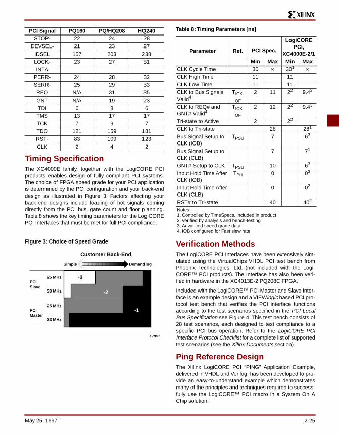
Timing SpecificationThe XC4000E family, together with the LogiCORE PCIproducts enables design of fully compliant PCI systems.The choice of FPGA speed grade for your PCI applicationis determined by the PCI configuration and your back-enddesign as illustrated in Figure 3. Factors affecting yourback-end designs include loading of hot signals comingdirectly from the PCI bus, gate count and floor planning.Table 8 shows the key timing parameters for the LogiCOREPCI Interfaces that must be met for full PCI compliance.
Figure 3: Choice of Speed Grade
Table 8: Timing Parameters [ns]
Verification MethodsThe LogiCORE PCI Interfaces have been extensively sim-ulated using the VirtualChips VHDL PCI test bench fromPhoenix Technologies, Ltd. (not included with the Logi-CORE™ PCI products). The Interface has also been veri-fied in hardware in the XC4013E-2 PQ208C FPGA.
Included with the LogiCORE™ PCI Master and Slave Inter-face is an example design and a VIEWlogic based PCI pro-tocol test bench that verifies the PCI interface functionsaccording to the test scenarios specified in the PCI LocalBus Specification see Figure 4. This test bench consists of28 test scenarios, each designed to test compliance to aspecific PCI bus operation. Refer to the LogiCORE PCIInterface Protocol Checklist for a complete list of supportedtest scenarios (see the Xilinx Documents section).
Ping Reference DesignThe Xilinx LogiCORE PCI “PING” Application Example,delivered in VHDL and Verilog, has been developed to pro-vide an easy-to-understand example which demonstratesmany of the principles and techniques required to success-fully use the LogiCORE™ PCI macro in a System On AChip solution.
STOP- 22 24 28DEVSEL- 21 23 27
IDSEL 157 203 238LOCK- 23 27 31INTA
PERR- 24 28 32SERR- 25 29 33REQ N/A 31 35GNT N/A 19 23TDI 6 8 6TMS 13 17 17TCK 7 9 7TDO 121 159 181RST- 83 109 123CLK 2 4 2
PCI Signal PQ160 PQ/HQ208 HQ240
X7952
-3PCISlave
25 MHz
Simple Demanding
Customer Back-End
33 MHz
PCIMaster
25 MHz
33 MHz
-2
-1
Parameter Ref. PCI Spec.
LogiCORE PCI,
XC4000E-2/1Min Max Min Max
CLK Cycle Time 30 ∞ 301 ∞CLK High Time 11 11CLK Low Time 11 11CLK to Bus Signals Valid4
TICK-
OF
2 11 22 9.43
CLK to REQ# and GNT# Valid4
TICK-
OF
2 12 22 9.43
Tri-state to Active 2 22
CLK to Tri-state 28 281
Bus Signal Setup to CLK (IOB)
TPSU 7 63
Bus Signal Setup to CLK (CLB)
7 71
GNT# Setup to CLK TPSU 10 63
Input Hold Time After CLK (IOB)
TPH 0 03
Input Hold Time After CLK (CLB)
0 02
RST# to Tri-state 40 402
Notes:1. Controlled by TimeSpecs, included in product2. Verified by analysis and bench-testing3. Advanced speed grade data4. IOB configured for Fast slew rate
May 25, 1997 2-25

PCI Master & Slave Interfaces Version 1.2.0PCI Master & Slave Interfaces Version 1.2.0
Figure 4: PCI Protocol Testbench
Recommended Design ExperienceThe LogiCORE PCI interface is pre-implemented allowingengineering focus at the unique back-end functions of aPCI design. Regardless, PCI is a high-performance systemthat is challenging to implement in any technology, ASIC orFPGA. Therefore, we recommend previous experience withbuilding high-performance, pipelined FPGA designs usingXilinx implementation software, Floorplanner, TIMESPECs,and guide files. The challenge to implement a complete PCIdesign including back-end functions varies depending onconfiguration and functionality of your application. Contactyour local Xilinx representative for a closer review and esti-mation for your specific requirements.
Table 9: Part Numbers
Ordering InformationTable 9 shows the part numbers for the LogiCORE™ prod-ucts. Before placing an order, please read and sign theattached LogiCORE™ license agreement and fax it to Xil-inx at +1 408-879-4780. For pricing and availability pleasecontact your local Xilinx sales office.
Related Information
Recommended Design CentersListed below are design centers and design consultantsthat have experience with the LogiCORE PCI products.
HighGate Design12380 Saratoga-Sunnyvale Road, Suite 8Saratoga, CA 95070-3090, USAPhone: +1 408-255-7160Fax: +1 408-255-7162E-mail: [email protected]: www.highgatedesign.com
Memec Design Services1819 S. Dobson Rd., Ste. 203Mesa, Arizona 85202, USAPhone: +1 602-491-4311Fax: +1 602-491-4907E-mail: [email protected]: www.memecdesign.com
Comit Systems1250 Oakmead Pkwy, Suite 210Sunnyvale, CA 94088, USAPhone: +1 408-988-2988Fax: +1 408-988-2133E-mail: [email protected]: www.comit.com
PCI Special Interest Group (PCI-SIG) PublicationsThe PCI-SIG publishes various PCI specifications andrelated documents such as PCI Local Bus Specification,PCI Compliance Checklist and PCI System Design Guide.
PCI Special Interest Group2575 NE Kathryn St #17Hillsboro, OR 97124Phone: +1 800-433-5177 (inside the US)
+1 503-693-6232 (outside the US)Fax: +1 503-693-8344Office hours: 8:30am - 4:00pm PSTE-mail: [email protected]: www.pcisig.com
Xilinx DocumentsMore PCI related information is available on Xilinx Web:www.xilinx.com/products/logicore/logicore.htm.
Product Part Number SupplierLogiCORETM PCI Master (Intiator/Tar-get)
LC-DI-PCIM-C Xilinx, Inc.
LogiCORETM PCI Slave (Target Only)
LC-DI-PCIS-C Xilinx, Inc.
LogiCOREPCI
Interface
SimpleArbiter
fakearb
lc_pci_i
TargetFunctional
Mode
faketarg testbnch
pci_test
InitiatorProtocolTest User
Application
X7951
2-26 May 25, 1997
Name:
(Signed) (Date)
Printed:
Title: Company:
Address:
E-mail: PO#:
Fax to: +1 408-879-4780 (USA)
PLEASE READ THIS DOCUMENT CAREFULLY BEFORE USING THE XIL-INX LOGICORE PCI MASTER INTERFACE OR PCI SLAVE INTERFACEDESIGN, BY USING THE XLINX LOGICORE DESIGN, YOU ARE AGREE-ING TO BE BOUND BY THE TERMS OF THIS LICENSE.
1. License. XLINX, INC. (“XILINX”) hereby grants you a nonexclusive, non-transferable license to use the LOGICORE PCI MASTER/SLAVE INTER-FACEdesign (the “Design”), solely for your use in developing designs forXLINX programmable logic devices or XLINX HardWire™ devices. Use ofthe Design in non-XILINX devices or technologies is prohibited unless youhave entered into a separate written agreement with XILINX for such use.XILINX retains title to the Design and to any patents, copyrights, tradesecrets and other intellectual property rights therein. To protect such intel-lectual property rights, you may not decompile, reverse engineer, disas-semble, or otherwise reduce the Design to a human-perceivable form. Youmay not modify or prepare derivative works of the Design in whole or inpart. This License allows you to make an unlimited number of copies of theDesign for internal use only, provided you reproduce on each copy of theDesign the copyright and any other proprietary legends that were on theoriginal copy of the Design.
2. Termination. This License is effective until terminated. You may terminatethis License at any time by destroying the Design and all copies thereof.This License will terminate immediately without notice from XILINX if youfail to comply with any provision of this License. Upon termination youmust destroy the Design and all copies thereof.
3. Governmental Use. The Design is commercial computer software devel-oped exclusively at Xilinx’s expense. Accordingly, pursuant to the FederalAcquisition Regulations (FAR) Section 12.212 and Defense FAR Supple-ment Section 227.2702, use, duplication and disclosure of the Design byor for the Government is subject to the restrictions set forth in this LicenseAgreement. Manufacturer is XILINX, INC., 2100 Logic Drive, San Jose,California 95124.
4. Limited Warranty and Disclaimer. THE DESIGN IS PROVIDED TO YOU“AS IS”. XILINX AND ITS LICENSORS MAKE AND YOU RECEIVE NOWARRANTIES OR CONDITIONS, EXPRESS, IMPLIED, STATUTORYOR OTHERWISE, AND XILINX SPECIFICALLY DISCLAIMS ANYIMPLIED WARRANTIES OF MERCHANTABILITY, NON-INFRINGE-MENT, OR FITNESS FOR A PARTICULAR PURPOSE. XILINX does notwarrant that the functions contained in the Design will meet your require-ments, or that the operation of the Design will be uninterrupted or errorfree, or that defects in the Design will be corrected. Furthermore, XILINX
does not warrant or make any representations regarding use or the resultsDesign in terms of correctness, accuracy, reliability or otherwise.
5. Limitation of Liability. IN NO EVENT WILL XILINX OR ITS LICENSORSBE LIABLE FOR ANY LOSS OF DATA, LOST PROFITS, COST OF PRO-CUREMENT OF SUBSTITUTE GOODS OR SERVICES, OR FOR ANYSPECIAL, INCIDENTAL, CONSEQUENTIAL OR INDIRECT DAMAGESARISING FROM THE USE OR OPERATION OF THE DESIGN ORACCOMPANYING DOCUMENTATION, HOWEVER CAUSED AND ONANY THEORY OF LIABILITY. THIS LIMITATIN WILL APPLY EVEN IF XIL-INX HAS BEEN ADVISED OF THE POSSIBILITY OF SUCH DAMAGE.THIS LIMITATION SHALL APPLY NOTWITHSTANDING THE FAILUREOF THE ESSENTIAL PURPOSE OF ANY LIMITED REMEDIES HEREIN.
6. Export Restriction. You agree that you will not export or re-export theDesign, reference images or accompanying documentation in any formwithout the appropriate United States and foreign government licenses.Your failure to comply with this provision is a material breach of this Agree-ment.
7. Third Party Beneficiary. You understand that portions of the Design andrelated documentation may have been licensed to XILINX from third par-ties and that such third parties are intended third party beneficiaries of theprovisions of this Agreement.
8. Non-Transferable. You may not provide design source information includ-ing, but not limited to, schematics, hardware description language sourcecode, or netlist files, to a third party without prior written approval from XIL-INX. You may provide device programming files— XILINX bit-stream filesor PROM files—of the resulting HardWire gate array to third-parties with-out prior approval.
9. General. This License shall be governed by the laws of the State of Cali-fornia, without reference to conflict of laws principles. If for any reason acourt of competent jurisdiction finds any provision of this License, or por-tion thereof, to be unenforceable, that provision of this License shall bereplaced to the maximum extent permissible so as to effectuate the intentof the parties, and the remainder of this License shall continue in full forceand effect. This License constitutes the entire agreement between the par-ties with respect to the use of this Design and related documentation, andsupersedes all prior or contemporaneous understandings or agreement,written or oral, regarding such subject matter.
I have read the Xilinx LogiCORE License Agreement, and I agreement to com-ply with the terms and conditions therein.
XILINX LOGICORE™ “PCI MASTER INTERFACE” AND“PCI SLAVE INTERFACE” LICENSE
AGREEMENT
May 25, 1997 2-27

PCI Master & Slave Interfaces Version 1.2.0PCI Master & Slave Interfaces Version 1.2.0
2-28 May 25, 1997
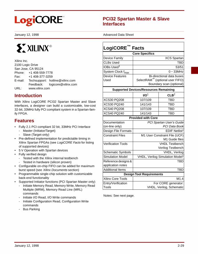
PCI32 Spartan Master & Slave Interfaces
January 12, 1998 Advanced Data Sheet
Xilinx Inc.2100 Logic DriveSan Jose, CA 95124Phone: +1 408-559-7778Fax: +1 408-377-3259E-mail: Techsupport: [email protected]
Feedback: [email protected]: www.xilinx.com
IntroductionWith Xilinx LogiCORE PCI32 Spartan Master and Slaveinterfaces, a designer can build a customizable, low-cost32-bit, 33MHz fully PCI compliant system in a Spartan-fam-ily FPGA.
Features• Fully 2.1 PCI compliant 32 bit, 33MHz PCI Interface
- Master (Initiator/Target)- Slave (Target-only)
• Pre-defined implementation for predictable timing in Xilinx Spartan FPGAs (see LogiCORE Facts for listing of supported devices)
• 5 V Operation with Spartan devices• Fully verified design
- Tested with the Xilinx internal testbench- Tested in hardware (silicon proven)
• Configurable on-chip FIFO can be added for maximum burst speed (see Xilinx Documents section)
• Programmable single-chip solution with customizable back-end functionality
• Supported Initiator functions (PCI Spartan Master only)- Initiate Memory Read, Memory Write, Memory Read
Multiple (MRM), Memory Read Line (MRL) commands
- Initiate I/O Read, I/O Write commands- Initiate Configuration Read, Configuration Write
commands- Bus Parking
R
LogiCORE ™ FactsCore Specifics
Device Family XCS SpartanCLBs Used TBDIOBs Used1 53/51System Clock fmax 0 − 33MHzDevice Features Used
Bi-directional data busesSelectRAM™ (optional user FIFO)
Boundary scan (optional)
Supported Devices/Resources Remaining
I/O1 CLB2
XCS30 PQ208 107/109 TBDXCS30 PQ240 141/143 TBDXCS40 PQ208 107/109 TBDXCS40 PQ240 141/143 TBD
Provided with CoreDocumentation (on-line only)
PCI Spartan User’s GuidePCI Data Book
Design File Formats EDIF Netlist3
Constraint Files M1 User Constraint File (UCF)M1 Guide files
Verification Tools VHDL TestbenchVerilog Testbench
Schematic Symbols VHDL, VerilogSimulation Model VHDL, Verilog Simulation Model3
Reference designs & application notes
TBD
Additional Items TBDDesign Tool Requirements
Xilinx Core Tools M1.4Entry/Verification Tools
For CORE generator:VHDL, Verilog, Schematic
Notes: See next page.
January 12, 1998 2-29
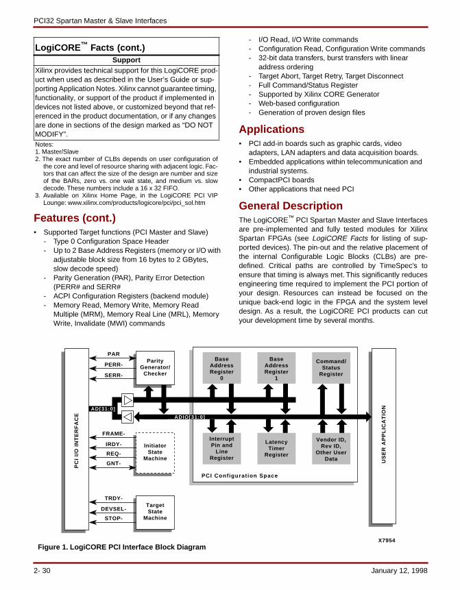
PCI32 Spartan Master & Slave Interfaces
Features (cont.)• Supported Target functions (PCI Master and Slave)
- Type 0 Configuration Space Header- Up to 2 Base Address Registers (memory or I/O with
adjustable block size from 16 bytes to 2 GBytes, slow decode speed)
- Parity Generation (PAR), Parity Error Detection (PERR# and SERR#
- ACPI Configuration Registers (backend module)- Memory Read, Memory Write, Memory Read
Multiple (MRM), Memory Real Line (MRL), Memory Write, Invalidate (MWI) commands
- I/O Read, I/O Write commands- Configuration Read, Configuration Write commands- 32-bit data transfers, burst transfers with linear
address ordering- Target Abort, Target Retry, Target Disconnect- Full Command/Status Register- Supported by Xilinx CORE Generator- Web-based configuration- Generation of proven design files
Applications• PCI add-in boards such as graphic cards, video
adapters, LAN adapters and data acquisition boards.• Embedded applications within telecommunication and
industrial systems.• CompactPCI boards• Other applications that need PCI
General DescriptionThe LogiCORE™ PCI Spartan Master and Slave Interfacesare pre-implemented and fully tested modules for XilinxSpartan FPGAs (see LogiCORE Facts for listing of sup-ported devices). The pin-out and the relative placement ofthe internal Configurable Logic Blocks (CLBs) are pre-defined. Critical paths are controlled by TimeSpec’s toensure that timing is always met. This significantly reducesengineering time required to implement the PCI portion ofyour design. Resources can instead be focused on theunique back-end logic in the FPGA and the system leveldesign. As a result, the LogiCORE PCI products can cutyour development time by several months.
LogiCORE ™ Facts (cont.)Support
Xilinx provides technical support for this LogiCORE prod-uct when used as described in the User’s Guide or sup-porting Application Notes. Xilinx cannot guarantee timing, functionality, or support of the product if implemented in devices not listed above, or customized beyond that ref-erenced in the product documentation, or if any changes are done in sections of the design marked as “DO NOT MODIFY”.Notes:1. Master/Slave2. The exact number of CLBs depends on user configuration of
the core and level of resource sharing with adjacent logic. Fac-tors that can affect the size of the design are number and sizeof the BARs, zero vs. one wait state, and medium vs. slowdecode. These numbers include a 16 x 32 FIFO.
3. Available on Xilinx Home Page, in the LogiCORE PCI VIPLounge: www.xilinx.com/products/logicore/pci/pci_sol.htm
ParityGenerator/
Checker
PAR
PERR-
SERR-
PCI Configuration Space
BaseAddressRegister
0
BaseAddressRegister
1
Command/Status
Register
InitiatorState
Machine
InterruptPin and
LineRegister
LatencyTimer
Register
Vendor ID,Rev ID,
Other UserData
X7954
TargetState
Machine
PC
I I/
O I
NT
ER
FA
CE
US
ER
AP
PL
ICA
TIO
N
ADIO[31:0]
AD[31:0]
GNT-
FRAME-
IRDY-
REQ-
TRDY-
DEVSEL-
STOP-
Figure 1. LogiCORE PCI Interface Block Diagram
2- 30 January 12, 1998
Xilinx Spartan Series FPGAs enables designs of fully PCI-compliant systems. The devices meet all required electricaland timing parameters including AC output drive character-istics, input capacitance specifications (10pF), 7 ns setupand 0 ns hold to system clock, and 11 ns system clock tooutput. These devices meet all specifications for 5 V PCI.
The PCI Compliance Checklist has additional details (seethe PCI Data Book). Other features that enable efficientimplementation of a complete PCI system in the Spartanfamily includes:
• Select-RAM™ memory: on-chip ultra-fast RAM with synchronous write option and dual-port RAM option. Used in the PCI Interfaces to implement the FIFO.
• Individual output enable for each I/O• Internal 3-state bus capability• 8 global low-skew clock or signal distribution networks• IEEE 1149.1-compatible boundary scan logic support
See Xilinx 1996 Data Book for more details.
The module is carefully optimized for best possible perfor-mance and utilization in the Spartan FPGA architecture.When implemented in the XC30, more than 50% of theFPGA’s resources remain for integrating a unique back-endinterface and other system functions into a fully program-mable one-chip solution.
Functional DescriptionThe LogiCORE PCI Master Interface is partitioned into fivemajor blocks, plus the user application, shown in Figure 1.Each block is described below.
PCI I/O Interface BlockThe I/O interface block handles the physical connection tothe PCI bus including all signaling, input and output syn-chronization, output three-state controls, and all request-grant handshaking for bus mastering.
Parity Generator/CheckerGenerates/checks even parity across the AD bus, the CBElines, and the PAR signal. Reports data parity errors viaPERR- and address parity errors via SERR-.
Target State MachineThis block manages control over the PCI interface for Tar-get functions. The states implemented are a subset ofequations defined in “Appendix B” of the PCI Local BusSpecification. The controller is a high-performance state
machine using state-per-bit (one-hot) encoding for maxi-mum performance. State-per-bit encoding has narrowerand shallower next-state logic functions that closely matchthe Xilinx FPGA architecture.
Initiator State Machine (PCI Master only)This block manages control over the PCI interface for Initia-tor functions. The states implemented are a subset of equa-tions defined in “Appendix B” of the PCI Local BusSpecification. The Initiator Control Logic also uses state-per-bit encoding for maximum performance.
PCI Configuration SpaceThis block provides the first 64 bytes of Type 0, version 2.1,Configuration Space Header (CSH) (see Table 1) to sup-port software-driven “Plug-and Play” initialization and con-figuration. This includes Command, Status, and two BaseAddress Registers (BARs). These BARs illustrate how toimplement memory- or I/O-mapped address spaces. EachBAR sets the base address for the interface and allows thesystem software to determine the addressable rangerequired by the interface. Using a combination of Config-urable Logic Block (CLB) flip-flops for the read/write regis-ters and CLB look-up tables for the read-only registersresults in optimized packing density and layout.
With this release, the hooks for extending configurationspace has been built into the backend interface. Setting theCapPtr and bit 15 of the Status Register allows the user toimplement functions such as Advanced Configuration andPower Interface (ACPI) in the backend design. The ACPImodule, whcih attaches to the backend, is included in thisrelease.
User Application with Optional Burst FIFOsThe LogiCORE PCI Interface provides a simple, general-purpose interface with a 32-bit data path and latchedaddress for de-multiplexing the PCI address/data bus. Thegeneral-purpose user interface allows the rest of the deviceto be used in a wide range of applications.
Typically, the user application contains burst FIFOs toincrease PCI system performance (An Application Note isavailable, please see the Xilinx Documents section). An on-chip read/write FIFO, built from the on-chip synchronousdual-port RAM (SelectRAM™) available in Spartandevices, supports data transfers in excess of 33 MHz.
January 12, 1998 2-31
PCI32 Spartan Master & Slave Interfaces
Table 1. PCI Configuration Space Header
Core ConfigurationThe LogiCORE PCI Interface can easily be configured to fitunique system requirements using Xilinx web-based PCICORE Generator. The following customization is supportedby the LogiCORE product and described in accompanyingdocumentation.
• Initiator or target functionality (PCI Master only)• Base Address Register configuration (1 - 3 Registers,
size and mode)• Configuration Space Header ROM• Initiator and target state machine (e.g., termination
conditions, transaction types and request/transaction arbitration)
• Burst functionality• User Application including FIFO (back-end design)
Table 2. PCI Bus Commands
Supported PCI CommandsTable 2 illustrates the PCI bus commands supported by theLogiCORE PCI Interface. The LogiCORE™ PCI InterfaceProtocol Checklist (2.1) has more details on supported andunsupported commands (see the PCI Data Book v2.0)
Burst TransferThe PCI bus derives its performance from its ability tosupport burst transfers. The performance of any PCIapplication depends largely on the size of the burst transfer.A FIFO to support PCI burst transfer can efficiently beimplemented using the Spartan on-chip RAM feature,SelectRAM™. Each Spartan CLB supports two 16x1 RAMblocks. This corresponds to 32 bits of single-ported RAM or16 bits of dual-ported RAM, with simultaneous read/writecapability.
Wait StatesIn this version of the core, only one wait state is supported.The XCS30-4 and XC40-4 are able to run with one waitstate. For zero wait state applications, use the LogiCOREPCI v2.0, implemented in XC4000XLT devices.
With one wait state, the LogiCORE Interface automaticallyinserts a wait state when sourcing data (Initiator Write, Tar-get Read) during a burst transfer. In this mode, the Logi-CORE Interface can accept data at 100% burst transferrate and supply data at 50%. See Table 3 for a PCI bustransfer rates for various operations.
31 16 15 0
Device ID Vendor ID 00h
Status Command 04h
Class Code Rev ID 08h
BIST Header Type
Latency Timer
Cache Line Size
0Ch
Base Address Register 0 (BAR0) 10h
Base Address Register 1 (BAR1) 14h
Base Address Register 2 (BAR2) 18h
Base Address Register 3 (BAR3) 1Ch
Base Address Register 4 (BAR5) 20h
Base Address Register 5 (BAR5) 24h
Cardbus CIS Pointer 28h
Subsystem ID Subsystem Vendor ID 2Ch
Expansion ROM Base Address 30h
Reserved CapPtr 34h
Reserved 38h
Max_Lat Min_Gnt Interrupt Pin
Interrupt Line
3Ch
Reserved 40h-FFh
Note: Italicized address areas are not implemented in the LogiCORE PCIInterface default configuration. These locations return zero duringconfiguration read accesses.
CBE[3:0]
CommandPCI
MasterPCI
Slave0000 Interrupt Acknowledge No1 Ignore0001 Special Cycle No1 Ignore0010 I/O Read Yes Yes0011 I/O Write Yes Yes0100 Reserved Ignore Ignore0101 Reserved Ignore Ignore0110 Memory Read Yes Yes0111 Memory Write Yes Yes1000 Reserved Ignore Ignore1001 Reserved Ignore Ignore1010 Configuration Read Yes Yes1011 Configuration Write Yes Yes1100 Memory Read Multiple Yes Yes1101 Dual Address Cycle No1 Ignore1110 Memory Read Line Yes Yes1111 Memory Write and Invalidate No1 Yes
Note:1. The Initiator can present these commands, however, they eitherrequire additional user-application logic to support them or havenot been thoroughly tested.
2- 32 January 12, 1998
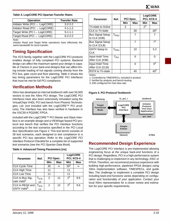
Table 3. LogiCORE PCI Spartan Transfer Rates
Timing SpecificationThe XCS family, together with the LogiCORE PCI productsenables design of fully compliant PCI systems. Backenddesign can affect the maximum speed your design is capa-ble of. Factors in your back-end designs that can affect tim-ing include loading of hot signals coming directly from thePCI bus, gate count and floor planning. Table 4 shows thekey timing parameters for the LogiCORE PCI Interfacesthat must be met for full PCI compliance.
Verification MethodsXilinx has developed an internal testbench with over 50,000vectors to test the Xilinx PCI design. The LogiCORE PCIInterfaces have also been extensively simulated using theVirtualChips VHDL PCI test bench from Phoenix Technolo-gies, Ltd. (not included with the LogiCORE™ PCI prod-ucts). The Interface has also been verified in hardware inthe XSC30-4 PQ208C FPGA.
Included with the LogiCORE™ PCI Master and Slave Inter-face is an example design and a VIEWlogic based PCI pro-tocol test bench that verifies the PCI interface functionsaccording to the test scenarios specified in the PCI LocalBus Specification see Figure 2. This test bench consists of28 test scenarios, each designed to test compliance to aspecific PCI bus operation. Refer to the LogiCORE PCIInterface Protocol Checklist for a complete list of supportedtest scenarios (see the PCI Spartan Data Book).
Table 4. Advanced Timing Parameters [ns]
Figure 2. PCI Protocol Testbench
Recommended Design ExperienceThe LogiCORE PCI interface is pre-implemented allowingengineering focus at the unique back-end functions of aPCI design. Regardless, PCI is a high-performance systemthat is challenging to implement in any technology, ASIC orFPGA. Therefore, we recommend previous experience withbuilding high-performance, pipelined FPGA designs usingXilinx implementation software, TIMESPECs, and guidefiles. The challenge to implement a complete PCI designincluding back-end functions varies depending on configu-ration and functionality of your application. Contact yourlocal Xilinx representative for a closer review and estima-tion for your specific requirements.
Operation Transfer RateInitiator Write (PCI ← LogiCORE) 3-2-2-2Initiator Read (PCI → LogiCORE) 4-1-1-2Target Write (PC I→ LogiCORE) 5-1-1-1Target Read (PCI ← LogiCORE) 6-2-2-2Note:Initiator Read and Target Write operations have effectively thesame bandwidth for burst transfer.
Parameter Ref. PCI Spec.LogiCORE PCI, XCS-4
Min Max Min MaxCLK Cycle Time 30 ∞ 301 ∞CLK High Time 11 11CLK Low Time 11 11CLK to Bus Sig-nals Valid3
TICK-
OF
2 11 22 9.6
CLK to REQ# and GNT# Valid3
TICK-
OF
2 12 22 9.6
Tri-state to Active 2 22
CLK to Tri-state 28 281
Bus Signal Setup to CLK (IOB)
TPSU 7 7
Bus Signal Setup to CLK (CLB)
7 71
GNT# Setup to CLK
TPSU 10 5.2
Input Hold Time After CLK (IOB)
TPH 0 0
Input Hold Time After CLK (CLB)
0 02
RST# to Tri-state 40 402
Notes:1. Controlled by TIMESPECs, included in product2. Verified by analysis and bench-testing3. IOB configured for Fast slew rate
Parameter Ref. PCI Spec.LogiCORE PCI, XCS-4
Min Max Min Max
LogiCOREPCI
Interface
SimpleArbiter
fakearb
lc_pci_i
TargetFunctional
Mode
faketarg testbnch
pci_test
InitiatorProtocolTest User
Application
X7951
January 12, 1998 2-33
PCI32 Spartan Master & Slave Interfaces
Table 5. Part Numbers
Ordering InformationTable 5 shows the part numbers for the LogiCORE™ prod-ucts. Before placing an order, please read and sign theattached LogiCORE™ license agreement and fax it to Xil-inx at +1 408-377-3259. For pricing and availability pleasecontact your local Xilinx sales office.
Related Information
Recommended Design CentersListed below are design centers and design consultantsthat have experience with the LogiCORE PCI products.
HighGate Design12380 Saratoga-Sunnyvale Road, Suite 8Saratoga, CA 95070-3090, USAPhone: +1 408-255-7160Fax: +1 408-255-7162E-mail: [email protected]: www.highgatedesign.com
Memec Design Services1819 S. Dobson Rd., Suite 203Mesa, Arizona 85202, USAPhone: +1 602-491-4311Fax: +1 602-491-4907E-mail: [email protected]: www.memecdesign.com
Comit Systems1250 Oakmead Pkwy, Suite 210Sunnyvale, CA 94088, USAPhone: +1 408-988-2987Fax: +1 408-988-2133E-mail: [email protected]: www.comit.com
Austin FranklinDark Room Technologies, Inc.126 Poor Farm RoadHarvard MA, 01451Phone: +1 508-772-9928Fax: +1 508-E-mail: [email protected]
PCI Special Interest Group (PCI-SIG) PublicationsThe PCI-SIG publishes various PCI specifications andrelated documents such as PCI Local Bus Specification,PCI Compliance Checklist and PCI System Design Guide.
PCI Special Interest Group2575 NE Kathryn St. #17Hillsboro, OR 97124Phone: +1 800-433-5177 (inside the US)
+1 503-693-6232 (outside the US)Fax: +1 503-693-8344Office hours: 8:30am - 4:00pm PSTE-mail: [email protected]: www.pcisig.com
Xilinx DocumentsMore PCI related information is available on Xilinx Web:
www.xilinx.com/products/logicore/logicore.htm.
Product Part NumberLogiCORETM PCI Spartan Master (Initia-tor/Target) LogiCORETM PCI Spartan Slave (Target Only)LogiCORETM PCI Spartan Slave to Master UpgradeLogiCORETM PCI Spartan Master (Initia-tor/Target) Software RenewalLogiCORETM PCI Spartan Slave (Target Only) Software Renewal
2- 34 January 12, 1998
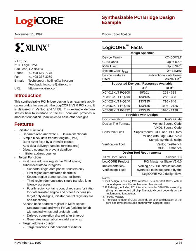
Synthesizable PCI Bridge Design Example
November 11, 1997 Product Specification
Xilinx Inc.2100 Logic DriveSan Jose, CA 95124Phone: +1 408-559-7778Fax: +1 408-377-3259E-mail: Techsupport: [email protected]
Feedback: [email protected]: http://www.xilinx.com
IntroductionThis synthesizable PCI bridge design is an example appli-cation bridge for use with the LogiCORE V2.0 PCI core. Itis delivered in Verilog and VHDL. This example demon-strates how to interface to the PCI core and provides amodular foundation upon which to base other designs.
Features• Initiator Functions
- Separate read and write FIFOs (unidirectional)- Simple block data transfer engine (DMA)- Burst sizes fixed by a transfer counter- Auto data delivery (handles terminations)- Discard counter to prevent deadlock- Initiator address counter
• Target Functions- First base address register in MEM space,
subdivided into four regions- Supports single data phase transfers only- First region demonstrates doorbells- Second region demonstrates mailboxes- Third region demonstrates single transfer, long
latency accesses- Fourth region contains control registers for initia-
tor data transfer engine and other functions (in target only designs, initiator control registers are non-functional)
- Second base address register in MEM space- Separate read and write FIFOs (unidirectional)
with posted writes and prefetch reads- Delayed completion discard after time-out - Generates target abort on address wrap
- Target address counter- Target functions independent of initiator
R
LogiCORE ™ FactsDesign Specifics
Device Family XC4000XLTCLBs Used Up to 8001
IOBs Used Up to 3202
System Clock fmax 0 − 33MHzDevice Features Used
Bi-directional data busesSelectRAM™
Supported Devices / Resources AvailableI/O3 CLB4
XC4013XLT PQ208 99/101 268 - 398XC4013XLT HQ240 133/135 268 - 398XC4028XLT HQ240 133/135 716 - 846XC4062XLT HQ240 133/135 1996 - 2126XC4062XLT BG432 293/295 1996 - 2126
Provided with DesignDocumentation User’s GuideDesign File Formats Verilog Source Code
VHDL Source CodeConstraint Files Supplemental .UCF and .PCF files
for use with LogiCORE V2.0Sample synthesis script
Verification Tool Verilog TestbenchVHDL Testbench
Design Tool RequirementsXilinx Core Tools Alliance 1.3LogiCORE Product PCI Master or Slave V2.0.0Implementation /Verification Tools
Verilog or VHDL simulation andsynthesis tools supported by the
LogiCORE V2.0 design flow.Notes:1. Full design, including PCI interface, is under 800 CLBs. Actual
count depends on the implemented feature set.2. Full design, including PCI interface, is under 320 IOBs assuming
all signals are routed off chip. The actual count depends on theimplemented feature set.
3. Target / Master.4. The exact number of CLBs depends on user configuration of the
core and level of resource sharing with adjacent logic.
November 11, 1997 2-35
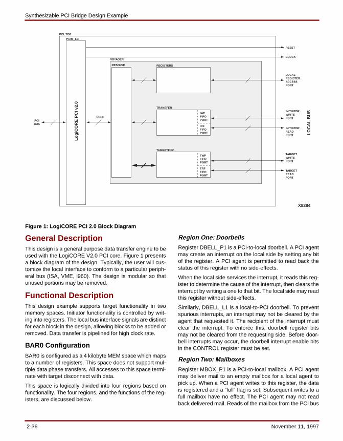
Synthesizable PCI Bridge Design Example
General DescriptionThis design is a general purpose data transfer engine to beused with the LogiCORE V2.0 PCI core. Figure 1 presentsa block diagram of the design. Typically, the user will cus-tomize the local interface to conform to a particular periph-eral bus (ISA, VME, i960). The design is modular so thatunused portions may be removed.
Functional DescriptionThis design example supports target functionality in twomemory spaces. Initiator functionality is controlled by writ-ing into registers. The local bus interface signals are distinctfor each block in the design, allowing blocks to be added orremoved. Data transfer is pipelined for high clock rate.
BAR0 ConfigurationBAR0 is configured as a 4 kilobyte MEM space which mapsto a number of registers. This space does not support mul-tiple data phase transfers. All accesses to this space termi-nate with target disconnect with data.
This space is logically divided into four regions based onfunctionality. The four regions, and the functions of the reg-isters, are discussed below.
Region One: Doorbells
Register DBELL_P1 is a PCI-to-local doorbell. A PCI agentmay create an interrupt on the local side by setting any bitof the register. A PCI agent is permitted to read back thestatus of this register with no side-effects.
When the local side services the interrupt, it reads this reg-ister to determine the cause of the interrupt, then clears theinterrupt by writing a one to that bit. The local side may readthis register without side-effects.
Similarly, DBELL_L1 is a local-to-PCI doorbell. To preventspurious interrupts, an interrupt may not be cleared by theagent that requested it. The recipient of the interrupt mustclear the interrupt. To enforce this, doorbell register bitsmay not be cleared from the requesting side. Before door-bell interrupts may occur, the doorbell interrupt enable bitsin the CONTROL register must be set.
Region Two: Mailboxes
Register MBOX_P1 is a PCI-to-local mailbox. A PCI agentmay deliver mail to an empty mailbox for a local agent topick up. When a PCI agent writes to this register, the datais registered and a “full” flag is set. Subsequent writes to afull mailbox have no effect. The PCI agent may not readback delivered mail. Reads of the mailbox from the PCI bus
Figure 1: LogiCORE PCI 2.0 Block Diagram
PCIBUS
PCI_TOP
PCIM_LC
VOYAGER
RESOLVE REGISTERS
TRANSFER
TARGETFIFO
IWFFIFOPORT
IRFFIFOPORT
TWFFIFOPORT
TRFFIFOPORT
RESET
CLOCK
LOCALREGISTERACCESSPORT
INITIATORWRITEPORT
INITIATORREADPORT
TARGETWRITEPORT
TARGETREADPORT
USER
Lo
giC
OR
E P
CI v
2.0
LO
CA
L B
US
X8284
2-36 November 11, 1997
side return the state of the full flag (replicated in all bits).
When the local side reads the mailbox, the “full” flag iscleared. Subsequent reads of an empty mailbox return thelast valid data present in the mailbox.
Similarly, MBOX_L1 is a local-to-PCI mailbox. The “full” flagmay be monitored in two ways. Mailbox “full” flags are al-ways observable in the CONTROL register, so both PCIagents and local agents may poll the CONTROL register towatch for new messages. Optionally, full mailboxes maycreate interrupts. Interrupts are created on the recipient’sside, and are cleared by reading the mailbox. Before mail-box interrupts may occur, the mailbox interrupt enable bitsin the CONTROL register must be set.
Region Three: Bounded Latency Accesses
The two registers in this region are used for demonstratingbounded latency non-burst accesses. This type of accessmay be used in situations where the user application has ashort latency with a known upper bound of 16 PCI clocksfrom the time the initiator asserts FRAME#. This is done byinserting wait states until the target is capable of completingthe transaction.
Register BL_CTRL controls the initial latency of read andwrite operations for itself and BL_DATA. Only the least-sig-nificant four bits of the register are implemented, and theregister is only accessible from the PCI bus. The local sidehas no access to this register, so local reads will return allzeroes and writes have no effect.
The second register, BL_DATA, is a general purpose, read/write register that responds according to the settings inBL_CTRL. This data register is only accessible from thePCI bus. The local side has no access to this register, solocal reads will return all zeroes and writes have no effect.
Region Four: Control Registers
The first three registers in this region control the initiatortransfer engine.
Register XFER_LEN is used to indicate the length of thedata block to be transferred. The low half of the register isnot implemented. The high half is implemented as a load-able 16-bit counter.
This register is accessible from both the PCI bus and localbus, and may be read at any time. Status of transfers inprogress may be obtained by reading this register. Witheach successful transfer, the counter decrements.
Register XFER_PADR contains the current PCI bus ad-dress for transfers performed by the transfer engine. De-pending on the direction of the transfer, this address maybe a source or destination.
This register is accessible from both the PCI bus and localbus, and may be read at any time. Status of transfers inprogress may be obtained by reading this register. Witheach successful transfer, the address increments.
Register XFER_LADR contains the current local addressfor transfers performed by the transfer engine. Dependingon the direction of the transfer, this address may be asource or destination. Only the low half of this register is im-plemented.
This register is accessible from both the PCI bus and localbus, and may be read at any time. Status of transfers inprogress may be obtained by reading this register. Witheach successful transfer, the address increments.
These registers must not be written to while the initiator isactive. To ensure this does not occur, writes to these regis-ter are disabled while the initiator is active.
BAR1 ConfigurationBAR1 is configured as a 64 kilobyte MEM space whichmaps to the target FIFOs. This space supports multipledata phase transfers. Transfers beyond the end of the ad-dress space result in target abort. For all other accesses,this region will respond according to how it is accessed.Consult the PCI specification regarding delayed transac-tions. Data transfer between the local side and PCI bus isachieved using retries and delayed transactions as needed.
Posted Writes
The target performs posted writes. On writes to an idle tar-get, the FIFO accepts incoming data until it is full or thewrite transaction has ended, whichever occurs first. In theevent of a full FIFO, the target issues a disconnect. After thePCI transaction is complete, the target empties the FIFO bywriting the data out to the local side until the FIFO is empty.To achieve this, the target latches the destination addressfor use during write out.
On writes to a busy target (the FIFO is still busy from theprevious transaction) the target responds with retry, withoutputting the request in a retry queue.
Prefetched Reads
For reads, the target may not anticipate the length of thetransaction or have the data available in time. For this rea-son, the target puts the transaction in a retry queue and re-sponds with a retry termination. Then the target prefetchesdata to fill the FIFO. When the initiator returns to retry thetransaction, the data will be available.
If the initiator returns to retry the transaction, and does notcompletely empty the FIFO, the FIFO is flushed after thetransaction is complete. If the initiator does empty the FIFO,and attempts to read more, the target issues a disconnect.
If the initiator never retries the original transaction, dead-lock may occur. For this reason, there exists a discard timerthat signals a waiting delayed completion should be dis-carded. This timer times out after 32,768 PCI clocks. Thisperiod may be shortened to allow simulation of this event ina reasonable amount of time.
November 11, 1997 2-37
Synthesizable PCI Bridge Design Example
Register File InterfaceThe operation of this block is synchronous to the PCI clock.This block contains all the control and status registers dis-cussed in the functional description. The local bus accessport is defined in Table 1.
Target FIFO InterfaceThe operation of this block is synchronous to the PCI clock.This block is interfaced to two FIFOs; one is the target read(TRF) FIFO, and the other is the target write (TWF) FIFO.
The FIFOs are identical, but data flows in opposite direc-tions. Table 2 lists the signals used in the interface.
Initiator FIFO InterfaceThe operation of this block is controlled by the contents ofregisters in the register block. This block is interfaced to twoFIFOs, similar to the memory interface block. One is the ini-tiator read (IRF) FIFO, and the other is the initiator write(IWF) FIFO.
The FIFOs are identical, but data flows in opposite direc-tions. A description of a FIFO follows in the FIFO section.Table 3 lists the signals used in the interface.
PinoutThe register file and FIFO interface pinouts are not fixed tospecific FPGA I/O pads, allowing flexibility in customization.The PCI bus specific signals are constrained as part of theLogiCORE PCI implementation.
As shipped, all of the register file and FIFO interface signalsare brought off-chip, but it is not necessary that any inter-face signals be brought off chip at all in single FPGA de-signs.
Core ModificationsModifications can be done to remove the initiator function-ality or selected portions of the target functionality. The fulldesign may be expanded as needed or reduced to a verysmall subset of the original design. The PCI interface itselfis also configurable by the designer.
Verification MethodsThis design example includes a system level testbench thatsimulates a four-slot PCI system. This simulation testbenchincludes a behavioral host bridge (with programmable arbi-ter) capable of generating burst transactions and a pro-grammable behavioral target.
Recommended Design ExperienceThe challenge to implement a complete PCI design variesdepending on configuration and functionality of your appli-cation. We recommend previous experience with buildinghigh-performance, pipelined FPGA designs using the Xilinximplementation software and familiarity with either VHDL orVerilog.
Ordering InformationThis design is available at no cost to all registered Logi-CORE V2.0 PCI core customers. It may be downloadedfrom the Xilinx home page. Simply log on to the CORESolutions section of WebLINX (http://www.xilinx.com/prod-ucts/logicore/logicore.htm) and select the appropriate link.
Table 1: Local Bus Register Interface
Name Direction FunctionLWE Input Write enable for regis-
tersLRE Input Read enable for regis-
tersLADDR Input Address input
LDIN Input Data inputLDOUT Output Data outputLINT_N Output Active low local inter-
rupt
Table 2: Local Bus Target FIFO Interface
Name Direction FunctionTRF_LDTWF_ST
OutputOutput
Data requested or avail-able
TRF_ADDRTWF_ADDR
OutputOutput
Transfer starting address
TRF_AF, TWF_AE Output Transfer almost done flagTRF_WR, TWF_RD Input FIFO write and read en-
ableTRF_DIN
TWF_DOUTInput
OutputData transfer ports
Table 3: Local Bus Initiator FIFO Interface
Name Direction FunctionIWF_LDIRF_ST
OutputOutput
Data requested or avail-able
IF_ADDR Output Transfer starting address
IWF_AF, IRF_AE Output Transfer almost done flagIWF_WR, IRF_RD Input FIFO write and read en-
ableIWF_DIN
IRF_DOUTInput
OutputData transfer ports
Table 3: Local Bus Initiator FIFO Interface
Name Direction Function
2-38 November 11, 1997
Digital Signal Processing Table of Contents
February 8, 1998
CorrelatorsOne Dimensional ROM-Based Correlator . . . . . . . . . . . . . . . . . . . . . . . . . . . . . . .2-41One Dimensional RAM-Based Correlator . . . . . . . . . . . . . . . . . . . . . . . . . . . . . . .2-45FiltersComb Filter . . . . . . . . . . . . . . . . . . . . . . . . . . . . . . . . . . . . . . . . . . . . . . . . . . . . . . .2-49Serial Distributed Arithmetic FIR Filter . . . . . . . . . . . . . . . . . . . . . . . . . . . . . . . . . .2-51Dual-Channel Serial Distributed Arithmetic FIR Filter . . . . . . . . . . . . . . . . . . . . . .2-55Parallel Distributed Arithmetic FIR Filter . . . . . . . . . . . . . . . . . . . . . . . . . . . . . . . .2-59TransformsDFT Cores (Real Data In, Complex Data Out) . . . . . . . . . . . . . . . . . . . . . . . . . . . .2-65FFT Core (1024 Points) . . . . . . . . . . . . . . . . . . . . . . . . . . . . . . . . . . . . . . . . . . . .2-69DSP Building BlocksSDA FIR Control Logic . . . . . . . . . . . . . . . . . . . . . . . . . . . . . . . . . . . . . . . . . . . . . .2-73Sine/Cosine . . . . . . . . . . . . . . . . . . . . . . . . . . . . . . . . . . . . . . . . . . . . . . . . . . . . . .2-75Non-Symmetric, 16-Deep Time Skew Buffer . . . . . . . . . . . . . . . . . . . . . . . . . . . . .2-77Non-Symmetric, 32-Deep Time Skew Buffer . . . . . . . . . . . . . . . . . . . . . . . . . . . . .2-81Symmetric, 16-Deep Time Skew Buffer . . . . . . . . . . . . . . . . . . . . . . . . . . . . . . . . .2-85
February 8, 1998 2-39
Digital Signal Processing Table of Contents
2-40 February 8, 1998
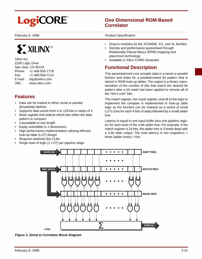
One Dimensional ROM-Based Correlator
February 8, 1998 Product Specification
Xilinx Inc.2100 Logic DriveSan Jose, CA 95124Phone: +1 408-559-7778Fax: +1 408-559-7114E-mail: [email protected]: www.xilinx.com
R
Features• Data can be loaded in either serial or parallel
(broadside) fashion• Supports data words from 4 to 128 bits in steps of 4• Mask register that selects which bits within the data
pattern to compare• Cascadable to any length• Easily extendible to 2 dimensions• High performance implementation utilizing efficient
look-up table (LUT) design• Requires relatively few CLBs• Single level of logic (1 LUT) per pipeline stage
• Drop-in modules for the XC4000E, EX, and XL families• Density and performance guaranteed through
Relationally Placed Macro (RPM) mapping and placement technology
• Available in Xilinx CORE Generator
Functional DescriptionThis parameterized core accepts data in a serial or parallelfashion and looks for a predetermined bit pattern that isstored in ROM look-up tables. The output is a binary repre-sentation of the number of bits that match the desired bitpattern after a bit mask has been applied to remove all ofthe “don’t care” bits.
The match register, the mask register, and all of the logic toimplement the compare is implemented in look-up tablelogic so the function can be realized as a series of smallLUTs (one for each 4 bits of data) followed by a small addertree.
Latency is equal to one input buffer plus one pipeline regis-ter for each level of the 4-bit adder tree. For example, if thematch register is 24 bits, the adder tree is 3 levels deep witha 5-bit wide output. The total latency is two (registers) +three (adder trees) = five.
DATA IN
SUM (n)
MASK REG
MATCH REG
SHIFT REG
INIT DATA
ΣX7983
Figure 1: Serial In Correlator Block Diagram
February 8, 1998 2-41
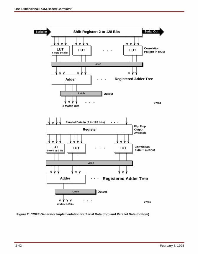
One Dimensional ROM-Based CorrelatorOne Dimensional ROM-Based Correlator
LUT4 word by 3 bit
LUT LUT
Latch
Registered Adder Tree
Output
Adder
Latch
# Match Bits
CorrelationPattern in ROM
Register
Parallel Data In (2 to 128 bits)Flip FlopOutputAvailable
X7985
Serial In
LUT4 word by 3 bit
LUT LUT
Latch
Registered Adder Tree
Output
Adder
Latch
# Match Bits
CorrelationPattern in ROM
Serial OutShift Register: 2 to 128 Bits
X7984
Figure 2: CORE Generator Implementation for Serial Data (top) and Parallel Data (bottom)
2-42 February 8, 1998
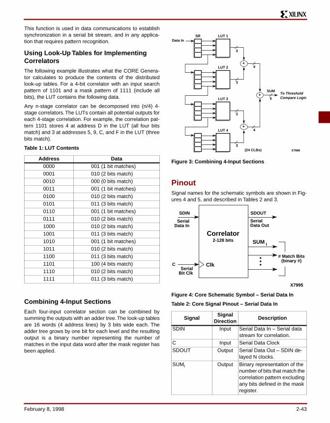
This function is used in data communications to establishsynchronization in a serial bit stream, and in any applica-tion that requires pattern recognition.
Using Look-Up Tables for Implementing CorrelatorsThe following example illustrates what the CORE Genera-tor calculates to produce the contents of the distributedlook-up tables. For a 4-bit correlator with an input searchpattern of 1101 and a mask pattern of 1111 (include allbits), the LUT contains the following data.
Any n-stage correlator can be decomposed into (n/4) 4-stage correlators. The LUTs contain all potential outputs foreach 4-stage correlation. For example, the correlation pat-tern 1101 stores 4 at address D in the LUT (all four bitsmatch) and 3 at addresses 5, 9, C, and F in the LUT (threebits match).
Table 1: LUT Contents
Combining 4-Input SectionsEach four-input correlator section can be combined bysumming the outputs with an adder tree. The look-up tablesare 16 words (4 address lines) by 3 bits wide each. Theadder tree grows by one bit for each level and the resultingoutput is a binary number representing the number ofmatches in the input data word after the mask register hasbeen applied.
Figure 3: Combining 4-Input Sections
PinoutSignal names for the schematic symbols are shown in Fig-ures 4 and 5, and described in Tables 2 and 3.
Figure 4: Core Schematic Symbol – Serial Data In
Table 2: Core Signal Pinout – Serial Data In
Address Data0000 001 (1 bit matches)0001 010 (2 bits match)0010 000 (0 bits match)0011 001 (1 bit matches)0100 010 (2 bits match)0101 011 (3 bits match)0110 001 (1 bit matches)0111 010 (2 bits match)1000 010 (2 bits match)1001 011 (3 bits match)1010 001 (1 bit matches)1011 010 (2 bits match)1100 011 (3 bits match)1101 100 (4 bits match)1110 010 (2 bits match)1111 011 (3 bits match)
SignalSignal
DirectionDescription
SDIN Input Serial Data In – Serial data stream for correlation.
C Input Serial Data ClockSDOUT Output Serial Data Out – SDIN de-
layed N clocks.SUMi Output Binary representation of the
number of bits that match the correlation pattern excluding any bits defined in the mask register.
+
+
+SUM
LUT 1
LUT 2
LUT 3
LUT 4
SRData In
3
3
3
3
4
4
5To ThresholdCompare Logic
(24 CLBs) X7986
Correlator2-128 bits
SerialData Out
SerialData In
SUM i
# Match Bits(binary #)
ClkC
SDIN SDOUT
SerialBit Clk
X7995
February 8, 1998 2-43

One Dimensional ROM-Based CorrelatorOne Dimensional ROM-Based Correlator
Figure 5: Core Schematic Symbol – Parallel Data In
Table 3: Core Signal Pinout – Parallel Data In
The CORE Generator accepts the parameters enteredthrough the dialog box and creates the specific design fromthe values entered using a parameterized VHDL recipe.VHDL instantiation code and a schematic symbol are cre-ated along with the netlist for the design.
CORE Generator ParametersThis macro has two CORE Generator dialog boxes. Theone for the parallel correlator is shown in Figure 6. Theserial correlator dialog box has a different title, but theparameters are the same. The parameters are as follows:
• Component Name : Enter a name for the component.• Data Width : Select an input width from the pull-down
menu for the data string to be compared. The valid range is 4-128 in multiples of 4.
• Match: Hexadecimal string specifying the pattern to look for.
• Mask: A zero in this hexadecimal string specifies that the data bit in the same position should be ignored when calculating the number of match bits.
• Radix : Hexadecimal or Binary representation of the Match and Mask values.
• Read From File : Read the Match and Mask values from a text file.
Figure 6: CORE Generator Dialog Box
Bit Width and CLB CountTable 4 lists the number of CLBs required for example bitwidths. The maximum speed is for XC4000E-1 devices.
Table 4: Bit Width versus CLB Count
Ordering InformationThis macro comes free with the Xilinx CORE Generator.For additional information contact your local Xilinx salesrepresentative, or e-mail requests to [email protected].
SignalSignal
DirectionDescription
DIN Input Parallel Data In – 2 to 128 bits
C Input Clock – Parallel load clockDOUT Output Parallel Data Out – DIN de-
layed 1 clock.SUMi Output Binary representation of the
number of bits that match the correlation pattern excluding any bits defined in the mask register.
DOUTDIN
Correlator2-128 bits
ParallelData Out
ParallelData In
SUM i
# Match Bits(binary #)
ClkCParallel
Load Clk
X7994
Bit Width CLB Count4 47 118 149 16
10 1711 1912 2013 2214 2415 2616 2517 2920 3632 54
2-44 February 8, 1998
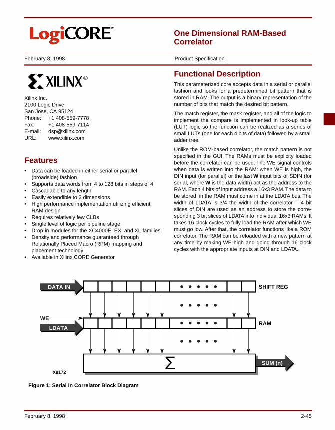
One Dimensional RAM-Based Correlator
February 8, 1998 Product Specification
Xilinx Inc.2100 Logic DriveSan Jose, CA 95124Phone: +1 408-559-7778Fax: +1 408-559-7114E-mail: [email protected]: www.xilinx.com
R
Features• Data can be loaded in either serial or parallel
(broadside) fashion• Supports data words from 4 to 128 bits in steps of 4• Cascadable to any length• Easily extendible to 2 dimensions• High performance implementation utilizing efficient
RAM design• Requires relatively few CLBs• Single level of logic per pipeline stage• Drop-in modules for the XC4000E, EX, and XL families• Density and performance guaranteed through
Relationally Placed Macro (RPM) mapping and placement technology
• Available in Xilinx CORE Generator
Functional DescriptionThis parameterized core accepts data in a serial or parallelfashion and looks for a predetermined bit pattern that isstored in RAM. The output is a binary representation of thenumber of bits that match the desired bit pattern.
The match register, the mask register, and all of the logic toimplement the compare is implemented in look-up table(LUT) logic so the function can be realized as a series ofsmall LUTs (one for each 4 bits of data) followed by a smalladder tree.
Unlike the ROM-based correlator, the match pattern is notspecified in the GUI. The RAMs must be explicity loadedbefore the correlator can be used. The WE signal controlswhen data is written into the RAM: when WE is high, theDIN input (for parallel) or the last W input bits of SDIN (forserial, where W is the data width) act as the address to theRAM. Each 4 bits of input address a 16x3 RAM. The data tobe stored in the RAM must come in at the LDATA bus. Thewidth of LDATA is 3/4 the width of the correlator -- 4 bitslices of DIN are used as an address to store the corre-sponding 3 bit slices of LDATA into individual 16x3 RAMs. Ittakes 16 clock cycles to fully load the RAM after which WEmust go low. After that, the correlator functions like a ROMcorrelator. The RAM can be reloaded with a new pattern atany time by making WE high and going through 16 clockcycles with the appropriate inputs at DIN and LDATA.
DATA IN
RAM
SHIFT REG
LDATA
X8172
SUM (n)Σ
WE
Figure 1: Serial In Correlator Block Diagram
February 8, 1998 2-45
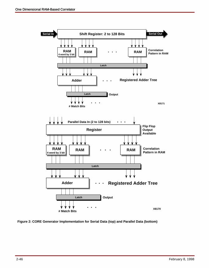
One Dimensional RAM-Based CorrelatorOne Dimensional RAM-Based Correlator
Serial In
RAM4 word by 3 bit
RAM RAM
Latch
Registered Adder Tree
Output
Adder
Latch
# Match Bits
CorrelationPattern in RAM
Serial OutShift Register: 2 to 128 Bits
X8171
RAM4 word by 3 bit
RAM RAM
Latch
Registered Adder Tree
Output
Adder
Latch
# Match Bits
CorrelationPattern in RAM
Register
Parallel Data In (2 to 128 bits)Flip FlopOutputAvailable
X8170
Figure 2: CORE Generator Implementation for Serial Data (top) and Parallel Data (bottom)
2-46 February 8, 1998
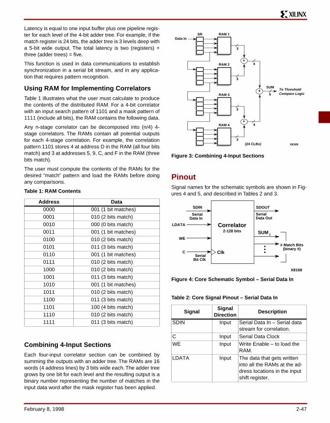
Latency is equal to one input buffer plus one pipeline regis-ter for each level of the 4-bit adder tree. For example, if thematch register is 24 bits, the adder tree is 3 levels deep witha 5-bit wide output. The total latency is two (registers) +three (adder trees) = five.
This function is used in data communications to establishsynchronization in a serial bit stream, and in any applica-tion that requires pattern recognition.
Using RAM for Implementing CorrelatorsTable 1 illustrates what the user must calculate to producethe contents of the distributed RAM. For a 4-bit correlatorwith an input search pattern of 1101 and a mask pattern of1111 (include all bits), the RAM contains the following data.
Any n-stage correlator can be decomposed into (n/4) 4-stage correlators. The RAMs contain all potential outputsfor each 4-stage correlation. For example, the correlationpattern 1101 stores 4 at address D in the RAM (all four bitsmatch) and 3 at addresses 5, 9, C, and F in the RAM (threebits match).
The user must compute the contents of the RAMs for thedesired “match” pattern and load the RAMs before doingany comparisons.
Table 1: RAM Contents
Combining 4-Input SectionsEach four-input correlator section can be combined bysumming the outputs with an adder tree. The RAMs are 16words (4 address lines) by 3 bits wide each. The adder treegrows by one bit for each level and the resulting output is abinary number representing the number of matches in theinput data word after the mask register has been applied.
Figure 3: Combining 4-Input Sections
PinoutSignal names for the schematic symbols are shown in Fig-ures 4 and 5, and described in Tables 2 and 3.
Figure 4: Core Schematic Symbol – Serial Data In
Table 2: Core Signal Pinout – Serial Data In
Address Data0000 001 (1 bit matches)0001 010 (2 bits match)0010 000 (0 bits match)0011 001 (1 bit matches)0100 010 (2 bits match)0101 011 (3 bits match)0110 001 (1 bit matches)0111 010 (2 bits match)1000 010 (2 bits match)1001 011 (3 bits match)1010 001 (1 bit matches)1011 010 (2 bits match)1100 011 (3 bits match)1101 100 (4 bits match)1110 010 (2 bits match)1111 011 (3 bits match)
SignalSignal
DirectionDescription
SDIN Input Serial Data In – Serial data stream for correlation.
C Input Serial Data ClockWE Input Write Enable – to load the
RAM.LDATA Input The data that gets written
into all the RAMs at the ad-dress locations in the input shift register.
+
+
+SUM
RAM 1
RAM 2
RAM 3
RAM 4
SRData In
3
3
3
3
4
4
5To ThresholdCompare Logic
(24 CLBs) X8169
Correlator2-128 bits
SerialData Out
SerialData In
SUM i
# Match Bits(binary #)
Clk
SDOUT
SerialBit Clk
X8168
LDATA
WE
C
SDIN
February 8, 1998 2-47
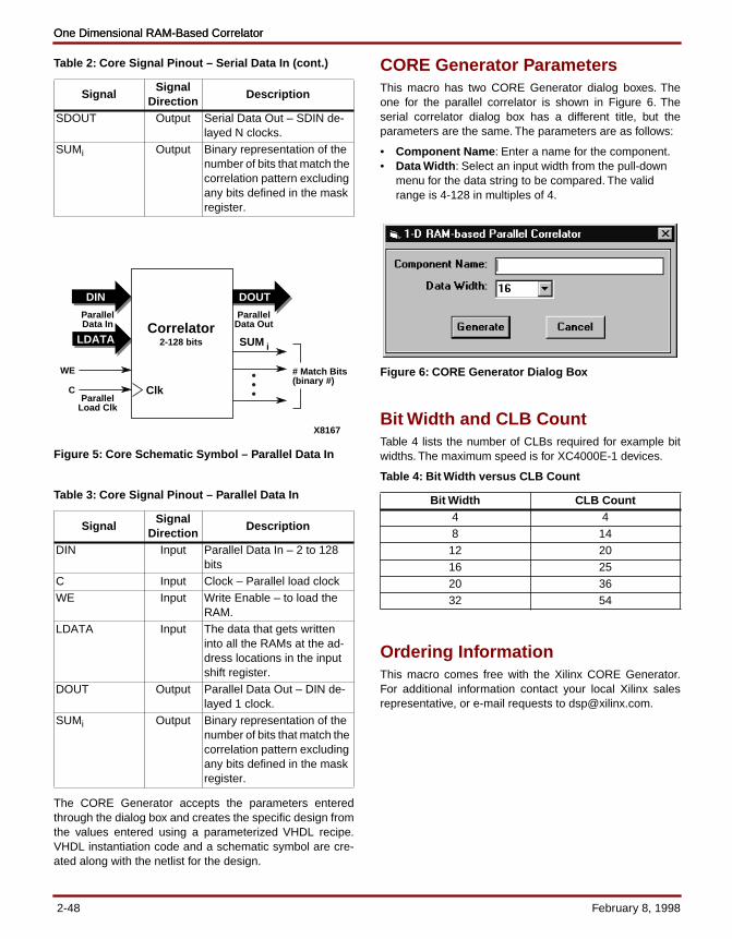
One Dimensional RAM-Based CorrelatorOne Dimensional RAM-Based Correlator
Table 2: Core Signal Pinout – Serial Data In (cont.)
Figure 5: Core Schematic Symbol – Parallel Data In
Table 3: Core Signal Pinout – Parallel Data In
The CORE Generator accepts the parameters enteredthrough the dialog box and creates the specific design fromthe values entered using a parameterized VHDL recipe.VHDL instantiation code and a schematic symbol are cre-ated along with the netlist for the design.
CORE Generator ParametersThis macro has two CORE Generator dialog boxes. Theone for the parallel correlator is shown in Figure 6. Theserial correlator dialog box has a different title, but theparameters are the same. The parameters are as follows:
• Component Name : Enter a name for the component.• Data Width : Select an input width from the pull-down
menu for the data string to be compared. The valid range is 4-128 in multiples of 4.
Figure 6: CORE Generator Dialog Box
Bit Width and CLB CountTable 4 lists the number of CLBs required for example bitwidths. The maximum speed is for XC4000E-1 devices.
Table 4: Bit Width versus CLB Count
Ordering InformationThis macro comes free with the Xilinx CORE Generator.For additional information contact your local Xilinx salesrepresentative, or e-mail requests to [email protected].
SignalSignal
DirectionDescription
SDOUT Output Serial Data Out – SDIN de-layed N clocks.
SUMi Output Binary representation of the number of bits that match the correlation pattern excluding any bits defined in the mask register.
SignalSignal
DirectionDescription
DIN Input Parallel Data In – 2 to 128 bits
C Input Clock – Parallel load clockWE Input Write Enable – to load the
RAM.LDATA Input The data that gets written
into all the RAMs at the ad-dress locations in the input shift register.
DOUT Output Parallel Data Out – DIN de-layed 1 clock.
SUMi Output Binary representation of the number of bits that match the correlation pattern excluding any bits defined in the mask register.
LDATA
DOUTDIN
Correlator2-128 bits
ParallelData Out
ParallelData In
SUM i
# Match Bits(binary #)
ClkCParallel
Load Clk
X8167
WE
Bit Width CLB Count4 48 14
12 2016 2520 3632 54
2-48 February 8, 1998
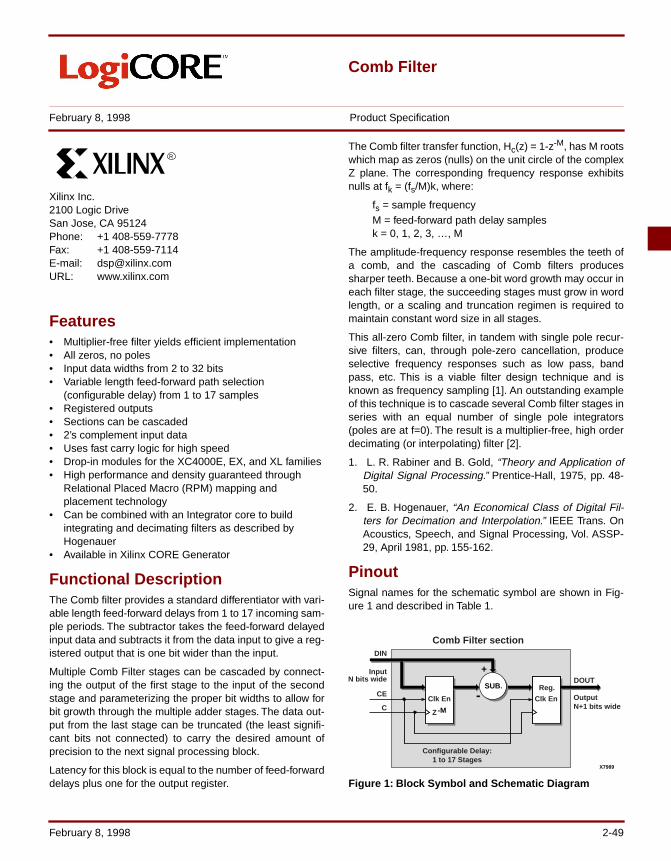
Comb Filter
February 8, 1998 Product Specification
Xilinx Inc.2100 Logic DriveSan Jose, CA 95124Phone: +1 408-559-7778Fax: +1 408-559-7114E-mail: [email protected]: www.xilinx.com
R
Features• Multiplier-free filter yields efficient implementation• All zeros, no poles • Input data widths from 2 to 32 bits• Variable length feed-forward path selection
(configurable delay) from 1 to 17 samples• Registered outputs• Sections can be cascaded • 2’s complement input data• Uses fast carry logic for high speed• Drop-in modules for the XC4000E, EX, and XL families• High performance and density guaranteed through
Relational Placed Macro (RPM) mapping and placement technology
• Can be combined with an Integrator core to build integrating and decimating filters as described by Hogenauer
• Available in Xilinx CORE Generator
Functional DescriptionThe Comb filter provides a standard differentiator with vari-able length feed-forward delays from 1 to 17 incoming sam-ple periods. The subtractor takes the feed-forward delayedinput data and subtracts it from the data input to give a reg-istered output that is one bit wider than the input.
Multiple Comb Filter stages can be cascaded by connect-ing the output of the first stage to the input of the secondstage and parameterizing the proper bit widths to allow forbit growth through the multiple adder stages. The data out-put from the last stage can be truncated (the least signifi-cant bits not connected) to carry the desired amount ofprecision to the next signal processing block.
Latency for this block is equal to the number of feed-forwarddelays plus one for the output register.
The Comb filter transfer function, Hc(z) = 1-z-M, has M rootswhich map as zeros (nulls) on the unit circle of the complexZ plane. The corresponding frequency response exhibitsnulls at fk = (fs/M)k, where:
fs = sample frequencyM = feed-forward path delay samplesk = 0, 1, 2, 3, …, M
The amplitude-frequency response resembles the teeth ofa comb, and the cascading of Comb filters producessharper teeth. Because a one-bit word growth may occur ineach filter stage, the succeeding stages must grow in wordlength, or a scaling and truncation regimen is required tomaintain constant word size in all stages.
This all-zero Comb filter, in tandem with single pole recur-sive filters, can, through pole-zero cancellation, produceselective frequency responses such as low pass, bandpass, etc. This is a viable filter design technique and isknown as frequency sampling [1]. An outstanding exampleof this technique is to cascade several Comb filter stages inseries with an equal number of single pole integrators(poles are at f=0). The result is a multiplier-free, high orderdecimating (or interpolating) filter [2].
1. L. R. Rabiner and B. Gold, “Theory and Application ofDigital Signal Processing.” Prentice-Hall, 1975, pp. 48-50.
2. E. B. Hogenauer, “An Economical Class of Digital Fil-ters for Decimation and Interpolation.” IEEE Trans. OnAcoustics, Speech, and Signal Processing, Vol. ASSP-29, April 1981, pp. 155-162.
PinoutSignal names for the schematic symbol are shown in Fig-ure 1 and described in Table 1.
Figure 1: Block Symbol and Schematic Diagram
SUB. Reg.
Clk En
+
-DOUT
OutputN+1 bits wide
DIN
InputN bits wide
CE
C
Configurable Delay:1 to 17 Stages
Comb Filter section
X7989
Clk En
Z-M
February 8, 1998 2-49
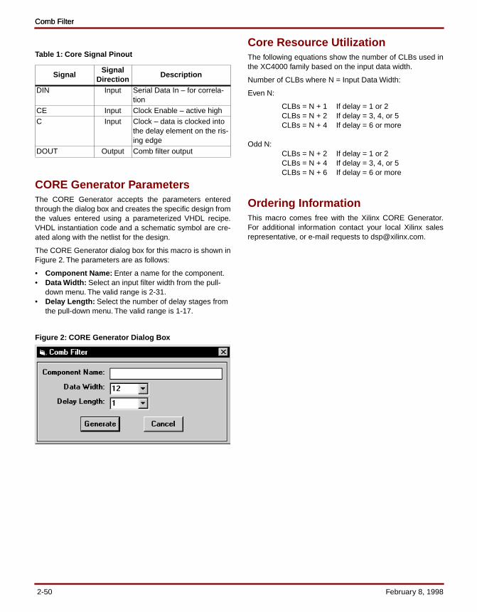
Comb FilterComb Filter
Table 1: Core Signal Pinout
CORE Generator ParametersThe CORE Generator accepts the parameters enteredthrough the dialog box and creates the specific design fromthe values entered using a parameterized VHDL recipe.VHDL instantiation code and a schematic symbol are cre-ated along with the netlist for the design.
The CORE Generator dialog box for this macro is shown inFigure 2. The parameters are as follows:
• Component Name: Enter a name for the component.• Data Width: Select an input filter width from the pull-
down menu. The valid range is 2-31.• Delay Length: Select the number of delay stages from
the pull-down menu. The valid range is 1-17.
Figure 2: CORE Generator Dialog Box
Core Resource UtilizationThe following equations show the number of CLBs used inthe XC4000 family based on the input data width.
Number of CLBs where N = Input Data Width:
Even N:
CLBs = N + 1 If delay = 1 or 2CLBs = N + 2 If delay = 3, 4, or 5CLBs = N + 4 If delay = 6 or more
Odd N:CLBs = N + 2 If delay = 1 or 2CLBs = N + 4 If delay = 3, 4, or 5CLBs = N + 6 If delay = 6 or more
Ordering InformationThis macro comes free with the Xilinx CORE Generator.For additional information contact your local Xilinx salesrepresentative, or e-mail requests to [email protected].
SignalSignal
DirectionDescription
DIN Input Serial Data In – for correla-tion
CE Input Clock Enable – active highC Input Clock – data is clocked into
the delay element on the ris-ing edge
DOUT Output Comb filter output
2-50 February 8, 1998
Serial Distributed Arithmetic FIR Filter
December 22, 1997 Product Specification
Xilinx Inc.2100 Logic DriveSan Jose, CA 95124Phone: +1 408-559-7778Fax: +1 408-559-7114E-mail: [email protected]: www.xilinx.com
R
Features• Input data words from 4 to 32 bits• Coefficient width from 4 to 24 bits• Output data words from 2 to 31 bits• Taps from 6 to 80 for symmetric filters• Taps from 6 to 40 for non-symmetric filters• Support for cascading multiple filters together to create
a larger filter • Support for symmetric, non-symmetric, and negative
symmetric filters• Full precision • Scaleable output• Input and output synchronization signals• Registered output• 2's complement input data• Uses Fast Carry logic for high speed• Drop-in modules for the XC4000E, EX, and XL families• High performance and density guaranteed through
Relational Placed Macro (RPM) mapping and placement technology
• Available in Xilinx CORE Generator
General DescriptionFIR filters are one of the most basic building blocks used indigital signal processing, taxing the performance that DSPhardware can deliver. Multiply accumulates must be per-formed at an ever-increasing rate and demands in the bil-lions of MACs per second range are now common.
Field programmable gate arrays (FPGAs) using distributedarithmetic algorithms can implement large numbers of tapsat MHz data sample rates, outperforming DSP processorsby one or two orders of magnitude. Sample rates can beefficiently handled over a wide range by applying the properstructure that just meets the required performance with theleast number of FPGA configurable logic blocks (CLBs).
Serial distributed arithmetic operates at relatively slowsample rates (3 to 15 million samples per second) but con-sumes few CLBs. Bits are processed serially, but all tapsare processed in parallel. If higher sample rates arerequired, structures are available which process 2, 3, 4, orall of the bits in parallel. Multi-rate FIR filters can also besupported, resulting in higher sample rates with the samenumber of resources.
Functional DescriptionThe FIR filter coefficients are formatted and stored in dis-tributed ROM memory (look-up tables) when the module isgenerated and full precision is maintained throughout allstages of arithmetic computation. Hand-shake signals areprovided to control the flow of data with a bit level clock.
The filter maintains full precision throughout processing.For example, a symmetrical 12-bit input data word and 14-bit coefficient would yield a 30-bit result (16-bit LUT + 2 bitsadder tree growth + 12-bits data + 1-bit subtracter minusone bit for saturation). The maximum available resolution isautomatically calculated by the SDA FIR dialog box afterthe balance of the other parameters have been entered andcan be displayed by looking at the pull-down menu for Out-put Data Width. The user can adjust the output to fewer bitsif desired. In the above example, the 30-bit number couldbe scaled to a 12-bit number if desired. Note that this doesnot significantly reduce the amount of logic required due tothe nature of the module design. The important factor isthat no noise is introduced into the system as a result ofarithmetic operations.
An SDA FIR filter processes data in a bit serial fashion. Thismeans that a data word of length N will require N clockcycles for a non-symmetric filter. This module processesALL taps of the filter in parallel and therefore requires onlyN clock cycles to process ALL of the filter’s taps. For a sym-metrical filter an additional clock cycle is required. For asymmetric SDA FIR the number of clock cycles is N+1 perfilter output. This will influence the frequency of the clock,C. The user must supply a clock which is at least N timesthe data sample rate for non-symmetric filters and N+1times the data rate for symmetric.
December 22, 1997 2-51
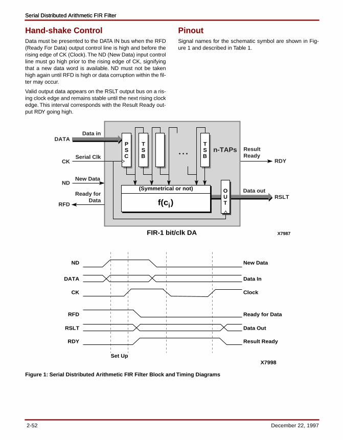
Serial Distributed Arithmetic FIR FilterSerial Distributed Arithmetic FIR Filter
Hand-shake ControlData must be presented to the DATA IN bus when the RFD(Ready For Data) output control line is high and before therising edge of CK (Clock). The ND (New Data) input controlline must go high prior to the rising edge of CK, signifyingthat a new data word is available. ND must not be takenhigh again until RFD is high or data corruption within the fil-ter may occur.
Valid output data appears on the RSLT output bus on a ris-ing clock edge and remains stable until the next rising clockedge. This interval corresponds with the Result Ready out-put RDY going high.
PinoutSignal names for the schematic symbol are shown in Fig-ure 1 and described in Table 1.
PSC
TSBSerial Clk
ND
DATA
RSLTReady forData
New Data
Data in
TSB
O
TU
(Symmetrical or not)
f(c )i
CK
RFD
ResultReady
RDY
Data out
n-TAPs
FIR-1 bit/clk DA X7987
X7998
ND
DATA
CK
RFD
RSLT
RDY
Set Up
New Data
Data In
Clock
Ready for Data
Data Out
Result Ready
Figure 1: Serial Distributed Arithmetic FIR Filter Block and Timing Diagrams
2-52 December 22, 1997
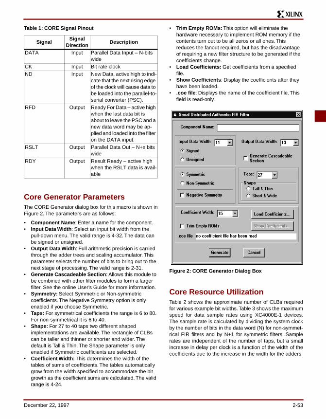
Table 1: CORE Signal Pinout
Core Generator ParametersThe CORE Generator dialog box for this macro is shown inFigure 2. The parameters are as follows:
• Component Name : Enter a name for the component.• Input Data Width : Select an input bit width from the
pull-down menu. The valid range is 4-32. The data can be signed or unsigned.
• Output Data Width : Full arithmetic precision is carried through the adder trees and scaling accumulator. This parameter selects the number of bits to bring out to the next stage of processing. The valid range is 2-31.
• Generate Cascadeable Section : Allows this module to be combined with other filter modules to form a larger filter. See the online User’s Guide for more information.
• Symmetry: Select Symmetric or Non-symmetric coefficients. The Negative Symmetry option is only enabled if you choose Symmetric.
• Taps: For symmetrical coefficients the range is 6 to 80. For non-symmetrical it is 6 to 40.
• Shape: For 27 to 40 taps two different shaped implementations are available. The rectangle of CLBs can be taller and thinner or shorter and wider. The default is Tall & Thin. The Shape parameter is only enabled if Symmetric coefficients are selected.
• Coefficient Width: This determines the width of the tables of sums of coefficients. The tables automatically grow from the width specified to accommodate the bit growth as the coefficient sums are calculated. The valid range is 4-24.
• Trim Empty ROMs: This option will eliminate the hardware necessary to implement ROM memory if the contents turn out to be all zeros or all ones. This reduces the fanout required, but has the disadvantage of requiring a new filter structure to be generated if the coefficients change.
• Load Coefficients: Get coefficients from a specified file.
• Show Coefficients : Display the coefficients after they have been loaded.
• .coe file : Displays the name of the coefficient file. This field is read-only.
Figure 2: CORE Generator Dialog Box
Core Resource UtilizationTable 2 shows the approximate number of CLBs requiredfor various example bit widths. Table 3 shows the maximumspeed for data sample rates using XC4000E-1 devices.The sample rate is calculated by dividing the system clockby the number of bits in the data word (N) for non-symmet-rical FIR filters and by N+1 for symmetric filters. Samplerates are independent of the number of taps, but a smallincrease in delay per clock is a function of the width of thecoefficients due to the increase in the width for the adders.
Signal Signal
DirectionDescription
DATA Input Parallel Data Input – N-bits wide
CK Input Bit rate clockND Input New Data, active high to indi-
cate that the next rising edge of the clock will cause data to be loaded into the parallel-to-serial converter (PSC).
RFD Output Ready For Data – active high when the last data bit is about to leave the PSC and a new data word may be ap-plied and loaded into the filter on the DATA input.
RSLT Output Parallel Data Out – N+x bits wide
RDY Output Result Ready – active high when the RSLT data is avail-able
December 22, 1997 2-53
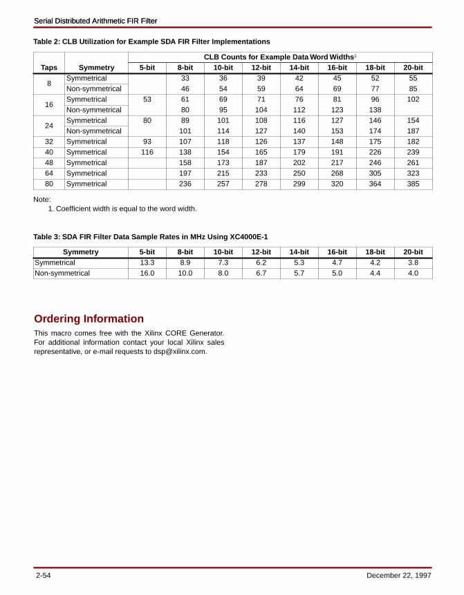
Serial Distributed Arithmetic FIR FilterSerial Distributed Arithmetic FIR Filter
Ordering InformationThis macro comes free with the Xilinx CORE Generator.For additional information contact your local Xilinx salesrepresentative, or e-mail requests to [email protected].
Table 2: CLB Utilization for Example SDA FIR Filter Implementations
Note:1. Coefficient width is equal to the word width.
Taps SymmetryCLB Counts for Example Data Word Widths 1
5-bit 8-bit 10-bit 12-bit 14-bit 16-bit 18-bit 20-bit
8Symmetrical 33 36 39 42 45 52 55Non-symmetrical 46 54 59 64 69 77 85
16Symmetrical 53 61 69 71 76 81 96 102Non-symmetrical 80 95 104 112 123 138
24Symmetrical 80 89 101 108 116 127 146 154Non-symmetrical 101 114 127 140 153 174 187
32 Symmetrical 93 107 118 126 137 148 175 18240 Symmetrical 116 138 154 165 179 191 226 23948 Symmetrical 158 173 187 202 217 246 26164 Symmetrical 197 215 233 250 268 305 32380 Symmetrical 236 257 278 299 320 364 385
Table 3: SDA FIR Filter Data Sample Rates in MHz Using XC4000E-1
Symmetry 5-bit 8-bit 10-bit 12-bit 14-bit 16-bit 18-bit 20-bitSymmetrical 13.3 8.9 7.3 6.2 5.3 4.7 4.2 3.8Non-symmetrical 16.0 10.0 8.0 6.7 5.7 5.0 4.4 4.0
2-54 December 22, 1997
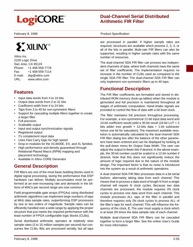
Dual-Channel Serial Distributed Arithmetic FIR Filter
February 8, 1998 Product Specification
Xilinx Inc.2100 Logic DriveSan Jose, CA 95124Phone: +1 408-559-7778Fax: +1 408-559-7114E-mail: [email protected]: www.xilinx.com
R
Features• Input data words from 4 to 16 bits• Output data words from 2 to 31 bits• Coefficient width from 4 to 24 bits• Taps from 3 to 40 for non-symmetric filters• Support for cascading multiple filters together to create
a larger filter • Full precision • Scaleable output• Input and output synchronization signals• Registered output• 2's complement input data• Uses Fast Carry logic for high speed• Drop-in modules for the XC4000E, EX, and XL families• High performance and density guaranteed through
Relational Placed Macro (RPM) mapping and placement technology
• Available in Xilinx CORE Generator
General DescriptionFIR filters are one of the most basic building blocks used indigital signal processing, taxing the performance that DSPhardware can deliver. Multiply accumulates must be per-formed at an ever-increasing rate and demands in the bil-lions of MACs per second range are now common.
Field programmable gate arrays (FPGAs) using distributedarithmetic algorithms can implement large numbers of tapsat MHz data sample rates, outperforming DSP processorsby one or two orders of magnitude. Sample rates can beefficiently handled over a wide range by applying the properstructure that just meets the required performance with theleast number of FPGA configurable logic blocks (CLBs).
Serial distributed arithmetic operates at relatively slowsample rates (3 to 15 million samples per second) but con-sumes few CLBs. Bits are processed serially, but all taps
are processed in parallel. If higher sample rates arerequired, structures are available which process 2, 3, 4, orall of the bits in parallel. Multi-rate FIR filters can also besupported, resulting in higher sample rates with the samenumber of resources.
The dual-channel SDA FIR filter can process two indepen-dent channels of data, where both channels have the sameset of filter coefficients. The implementation requires noincrease in the number of CLBs used as compared to thesingle SDA FIR filter. The dual-channel SDA FIR filter canonly implement non-symmetric filters up to 40 taps.
Functional DescriptionThe FIR filter coefficients are formatted and stored in dis-tributed ROM memory (look-up tables) when the module isgenerated and full precision is maintained throughout allstages of arithmetic computation. Hand-shake signals areprovided to control the flow of data with a bit level clock.
The filter maintains full precision throughout processing.For example, a non-symmetrical 12-bit input data word and14-bit coefficient would yield a 30-bit result (16-bit LUT + 2bits adder tree growth + 12-bits data + 1-bit subtracterminus one bit for saturation). The maximum available reso-lution is automatically calculated by the dual-channel SDAFIR filter dialog box after the balance of the other parame-ters have been entered and can be displayed by looking atthe pull-down menu for Output Data Width. The user canadjust the output to fewer bits if desired. In the above exam-ple, the 30-bit number could be scaled to a 12-bit number ifdesired. Note that this does not significantly reduce theamount of logic required due to the nature of the moduledesign. The important factor is that no noise is introducedinto the system as a result of arithmetic operations.
A dual-channel SDA FIR filter processes data in a bit serialfashion, alternately taking data from each channel. Thismeans that to process a data word of length N from a singlechannel will require N clock cycles. Because two datachannels are processed, the module requires 2N clockcycles to process one data word from each channel. Thismodule processes ALL taps of the filter in parallel andtherefore requires only 2N clock cycles to process ALL ofthe filter’s taps for each channel. This will influence the fre-quency of the clock, C. The user must supply a clock whichis at least 2N times the data sample rate of each channel.
Multiple dual-channel SDA FIR filters can be cascadedtogether to form a larger filter. See the online User’s Guidefor more information.
February 8, 1998 2-55
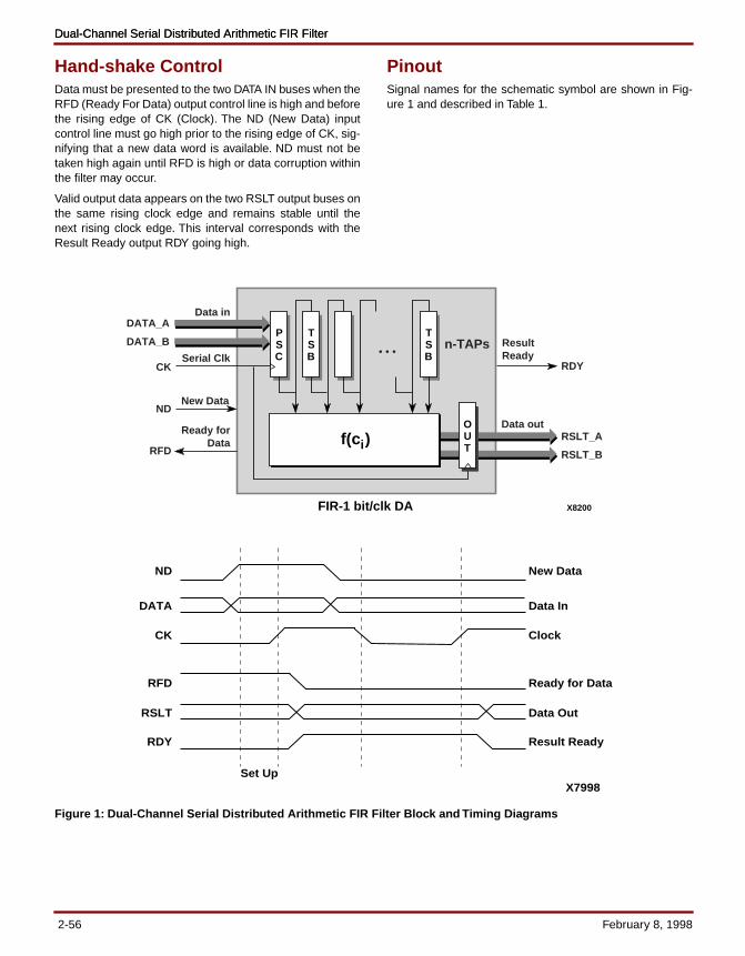
Dual-Channel Serial Distributed Arithmetic FIR FilterDual-Channel Serial Distributed Arithmetic FIR Filter
Hand-shake ControlData must be presented to the two DATA IN buses when theRFD (Ready For Data) output control line is high and beforethe rising edge of CK (Clock). The ND (New Data) inputcontrol line must go high prior to the rising edge of CK, sig-nifying that a new data word is available. ND must not betaken high again until RFD is high or data corruption withinthe filter may occur.
Valid output data appears on the two RSLT output buses onthe same rising clock edge and remains stable until thenext rising clock edge. This interval corresponds with theResult Ready output RDY going high.
PinoutSignal names for the schematic symbol are shown in Fig-ure 1 and described in Table 1.
X7998
ND
DATA
CK
RFD
RSLT
RDY
Set Up
New Data
Data In
Clock
Ready for Data
Data Out
Result Ready
PSC
TSBSerial Clk
ND
DATA_A
Ready forData
New Data
Data in
TSB
RSLT_A
CK
RFD
ResultReady
RDY
Data out
n-TAPs
FIR-1 bit/clk DA X8200
RSLT_B
O
TUf(c )i
DATA_B
Figure 1: Dual-Channel Serial Distributed Arithmetic FIR Filter Block and Timing Diagrams
2-56 February 8, 1998
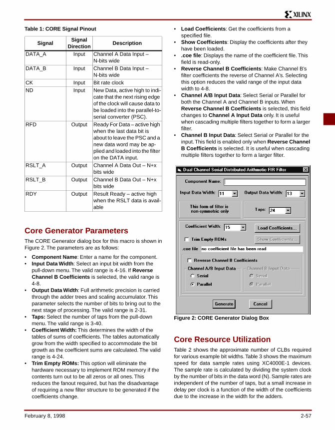
Table 1: CORE Signal Pinout
Core Generator ParametersThe CORE Generator dialog box for this macro is shown inFigure 2. The parameters are as follows:
• Component Name : Enter a name for the component.• Input Data Width : Select an input bit width from the
pull-down menu. The valid range is 4-16. If Reverse Channel B Coefficients is selected, the valid range is 4-8.
• Output Data Width : Full arithmetic precision is carried through the adder trees and scaling accumulator. This parameter selects the number of bits to bring out to the next stage of processing. The valid range is 2-31.
• Taps: Select the number of taps from the pull-down menu. The valid range is 3-40.
• Coefficient Width: This determines the width of the tables of sums of coefficients. The tables automatically grow from the width specified to accommodate the bit growth as the coefficient sums are calculated. The valid range is 4-24.
• Trim Empty ROMs: This option will eliminate the hardware necessary to implement ROM memory if the contents turn out to be all zeros or all ones. This reduces the fanout required, but has the disadvantage of requiring a new filter structure to be generated if the coefficients change.
• Load Coefficients : Get the coefficients from a specified file.
• Show Coefficients : Display the coefficients after they have been loaded.
• .coe file : Displays the name of the coefficient file. This field is read-only.
• Reverse Channel B Coefficients : Make Channel B’s filter coefficients the reverse of Channel A’s. Selecting this option reduces the valid range of the input data width to 4-8.
• Channel A/B Input Data : Select Serial or Parallel for both the Channel A and Channel B inputs. When Reverse Channel B Coefficients is selected, this field changes to Channel A Input Data only. It is useful when cascading multiple filters together to form a larger filter.
• Channel B Input Data : Select Serial or Parallel for the input. This field is enabled only when Reverse Channel B Coefficients is selected. It is useful when cascading multiple filters together to form a larger filter.
Figure 2: CORE Generator Dialog Box
Core Resource UtilizationTable 2 shows the approximate number of CLBs requiredfor various example bit widths. Table 3 shows the maximumspeed for data sample rates using XC4000E-1 devices.The sample rate is calculated by dividing the system clockby the number of bits in the data word (N). Sample rates areindependent of the number of taps, but a small increase indelay per clock is a function of the width of the coefficientsdue to the increase in the width for the adders.
Signal Signal
DirectionDescription
DATA_A Input Channel A Data Input – N-bits wide
DATA_B Input Channel B Data Input – N-bits wide
CK Input Bit rate clockND Input New Data, active high to indi-
cate that the next rising edge of the clock will cause data to be loaded into the parallel-to-serial converter (PSC).
RFD Output Ready For Data – active high when the last data bit is about to leave the PSC and a new data word may be ap-plied and loaded into the filter on the DATA input.
RSLT_A Output Channel A Data Out – N+x bits wide
RSLT_B Output Channel B Data Out – N+x bits wide
RDY Output Result Ready – active high when the RSLT data is avail-able
February 8, 1998 2-57
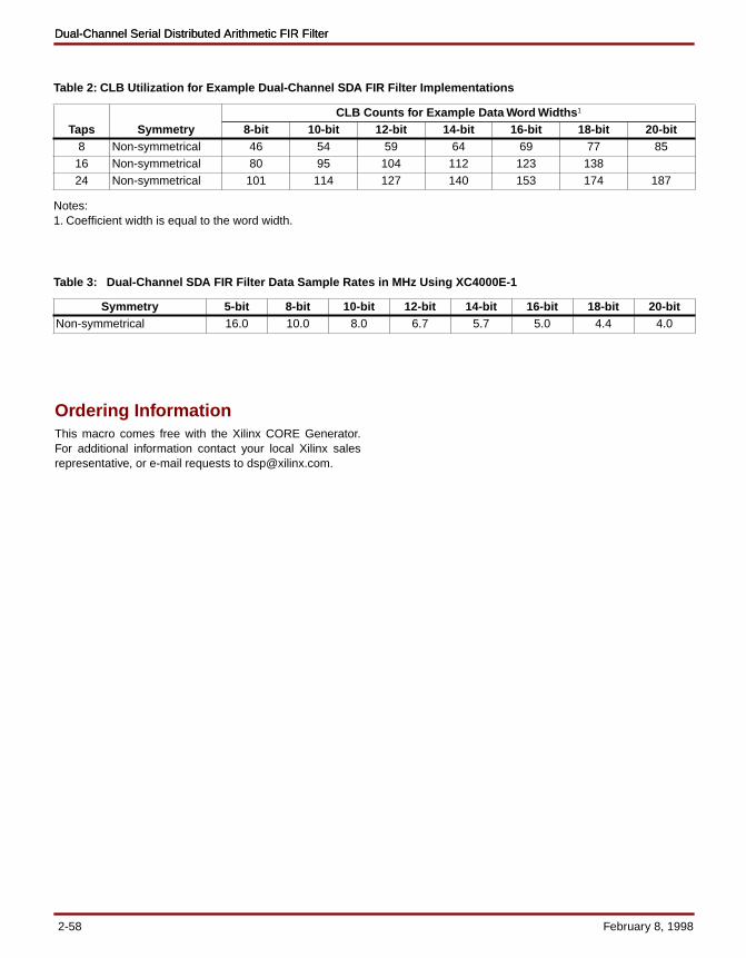
Dual-Channel Serial Distributed Arithmetic FIR FilterDual-Channel Serial Distributed Arithmetic FIR Filter
Ordering InformationThis macro comes free with the Xilinx CORE Generator.For additional information contact your local Xilinx salesrepresentative, or e-mail requests to [email protected].
Table 2: CLB Utilization for Example Dual-Channel SDA FIR Filter Implementations
Notes:1. Coefficient width is equal to the word width.
Taps SymmetryCLB Counts for Example Data Word Widths 1
8-bit 10-bit 12-bit 14-bit 16-bit 18-bit 20-bit8 Non-symmetrical 46 54 59 64 69 77 85
16 Non-symmetrical 80 95 104 112 123 13824 Non-symmetrical 101 114 127 140 153 174 187
Table 3: Dual-Channel SDA FIR Filter Data Sample Rates in MHz Using XC4000E-1
Symmetry 5-bit 8-bit 10-bit 12-bit 14-bit 16-bit 18-bit 20-bitNon-symmetrical 16.0 10.0 8.0 6.7 5.7 5.0 4.4 4.0
2-58 February 8, 1998
Parallel Distributed Arithmetic FIR Filter
February 8, 1998 Product Specification
Xilinx Inc.2100 Logic DriveSan Jose, CA 95124Phone: +1 408-559-7778Fax: +1 408-559-7114E-mail: [email protected]: www.xilinx.com
R
Features• Input data words from 4 to 32 bits• Coefficient width from 4 to 24 bits• Output data words from 2 to 31 bits• Taps from 2 to 20 for symmetric filters• Taps from 2 to 10 for non-symmetric filters• Support for cascading multiple filters together to create
a larger filter • Support for symmetric, non-symmetric, and negative
symmetric filters• Full precision • Scaleable output• Input and output synchronization signals• Registered output• 2's complement input data• Uses Fast Carry logic for high speed• Drop-in modules for the XC4000E, EX, and XL families• High performance and density guaranteed through
Relational Placed Macro (RPM) mapping and placement technology
• Available in Xilinx CORE Generator
General DescriptionFIR filters are one of the most basic building blocks used indigital signal processing, taxing the performance that DSPhardware can deliver. Multiply accumulates must be per-
formed at an ever-increasing rate and demands in the bil-lions of MACs per second range are now common.
Field programmable gate arrays (FPGAs) using distributedarithmetic algorithms can implement large numbers of tapsat MHz data sample rates, outperforming DSP processorsby one or two orders of magnitude. Sample rates can beefficiently handled over a wide range by applying the properstructure that just meets the required performance with theleast number of FPGA configurable logic blocks (CLBs).
Functional DescriptionThe FIR filter coefficients are formatted and stored in dis-tributed ROM memory (look-up tables) when the module isgenerated and full precision is maintained throughout allstages of arithmetic computation.
The filter maintains full precision throughout processing.For example, a symmetrical 8-tap filter processing 12-bitinput data words and 8-bit coefficients would yield a 24-bitresult. The maximum available resolution is automaticallycalculated by the PDA FIR dialog box after the balance ofthe other parameters have been entered and can be dis-played by looking at the pull-down menu for Output DataWidth. The user can adjust the output to fewer bits ifdesired. In the above example, the 24-bit number could bescaled to a 12-bit number if desired. Note that this does notsignificantly reduce the amount of logic required due to thenature of the module design. The important factor is that nonoise is introduced into the system as a result of arithmeticoperations.
A PDA FIR filter processes data in parallel. This means thatit can process a new data word every clock cycle.
Valid output data appears on the DATA_OUT output bus ona rising clock edge and remains stable until the next risingclock edge.
PinoutSignal names for the schematic symbol are shown in Fig-ures 1 and 2 and described in Table 1.
February 8, 1998 2-59
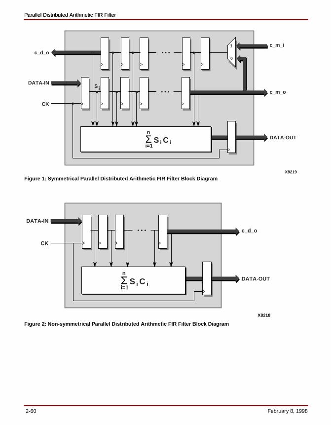
Parallel Distributed Arithmetic FIR FilterParallel Distributed Arithmetic FIR Filter
DATA-IN
DATA-OUT
CK
c_d_o
X8218
Σ iS iCi=1
n
DATA-IN
DATA-OUT
CK
c_m_o
X8219
Σ iS iCi=1
n
c_d_o1
0
c_m_i
S i
Figure 1: Symmetrical Parallel Distributed Arithmetic FIR Filter Block Diagram
Figure 2: Non-symmetrical Parallel Distributed Arithmetic FIR Filter Block Diagram
2-60 February 8, 1998
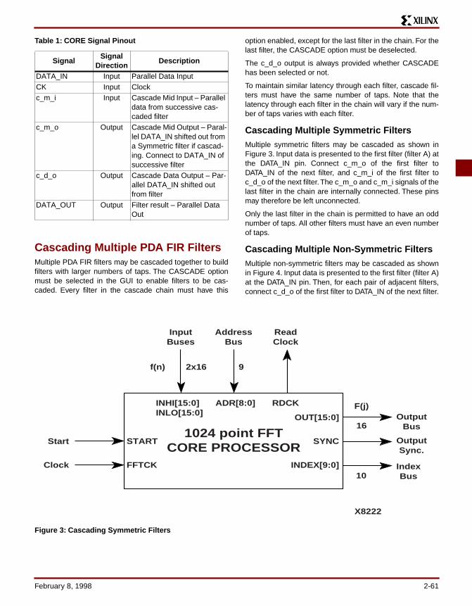
Table 1: CORE Signal Pinout
Cascading Multiple PDA FIR FiltersMultiple PDA FIR filters may be cascaded together to buildfilters with larger numbers of taps. The CASCADE optionmust be selected in the GUI to enable filters to be cas-caded. Every filter in the cascade chain must have this
option enabled, except for the last filter in the chain. For thelast filter, the CASCADE option must be deselected.
The c_d_o output is always provided whether CASCADEhas been selected or not.
To maintain similar latency through each filter, cascade fil-ters must have the same number of taps. Note that thelatency through each filter in the chain will vary if the num-ber of taps varies with each filter.
Cascading Multiple Symmetric FiltersMultiple symmetric filters may be cascaded as shown inFigure 3. Input data is presented to the first filter (filter A) atthe DATA_IN pin. Connect c_m_o of the first filter toDATA_IN of the next filter, and c_m_i of the first filter toc_d_o of the next filter. The c_m_o and c_m_i signals of thelast filter in the chain are internally connected. These pinsmay therefore be left unconnected.
Only the last filter in the chain is permitted to have an oddnumber of taps. All other filters must have an even numberof taps.
Cascading Multiple Non-Symmetric FiltersMultiple non-symmetric filters may be cascaded as shownin Figure 4. Input data is presented to the first filter (filter A)at the DATA_IN pin. Then, for each pair of adjacent filters,connect c_d_o of the first filter to DATA_IN of the next filter.
Figure 3: Cascading Symmetric Filters
Signal Signal
DirectionDescription
DATA_IN Input Parallel Data InputCK Input Clockc_m_i Input Cascade Mid Input – Parallel
data from successive cas-caded filter
c_m_o Output Cascade Mid Output – Paral-lel DATA_IN shifted out from a Symmetric filter if cascad-ing. Connect to DATA_IN of successive filter
c_d_o Output Cascade Data Output – Par-allel DATA_IN shifted out from filter
DATA_OUT Output Filter result – Parallel Data Out
START
FFTCK
Start
Clock
1024 point FFT CORE PROCESSOR
OUT[15:0]
SYNC
INDEX[9:0]
INHI[15:0]INLO[15:0]
InputBuses
AddressBus
ReadClock
f(n) 2x16
ADR[8:0] RDCK
OutputBus
OutputSync.
IndexBus
X8222
F(j)
16
9
10
February 8, 1998 2-61
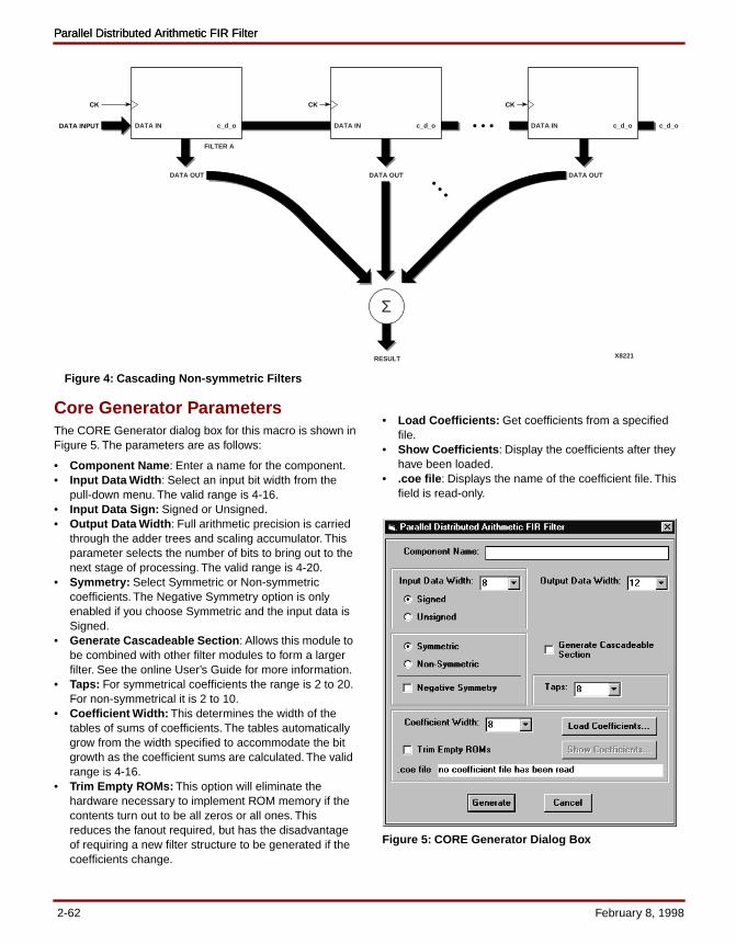
Parallel Distributed Arithmetic FIR FilterParallel Distributed Arithmetic FIR Filter
Core Generator ParametersThe CORE Generator dialog box for this macro is shown inFigure 5. The parameters are as follows:
• Component Name : Enter a name for the component.• Input Data Width : Select an input bit width from the
pull-down menu. The valid range is 4-16. • Input Data Sign: Signed or Unsigned. • Output Data Width : Full arithmetic precision is carried
through the adder trees and scaling accumulator. This parameter selects the number of bits to bring out to the next stage of processing. The valid range is 4-20.
• Symmetry: Select Symmetric or Non-symmetric coefficients. The Negative Symmetry option is only enabled if you choose Symmetric and the input data is Signed.
• Generate Cascadeable Section : Allows this module to be combined with other filter modules to form a larger filter. See the online User’s Guide for more information.
• Taps: For symmetrical coefficients the range is 2 to 20. For non-symmetrical it is 2 to 10.
• Coefficient Width: This determines the width of the tables of sums of coefficients. The tables automatically grow from the width specified to accommodate the bit growth as the coefficient sums are calculated. The valid range is 4-16.
• Trim Empty ROMs: This option will eliminate the hardware necessary to implement ROM memory if the contents turn out to be all zeros or all ones. This reduces the fanout required, but has the disadvantage of requiring a new filter structure to be generated if the coefficients change.
• Load Coefficients: Get coefficients from a specified file.
• Show Coefficients : Display the coefficients after they have been loaded.
• .coe file : Displays the name of the coefficient file. This field is read-only.
Figure 5: CORE Generator Dialog Box
CK
DATA INPUT
CK CK
c_d_oc_d_oDATA INc_d_oDATA INc_d_oDATA IN
DATA OUTDATA OUTDATA OUT
Σ
RESULT X8221
FILTER A
Figure 4: Cascading Non-symmetric Filters
2-62 February 8, 1998
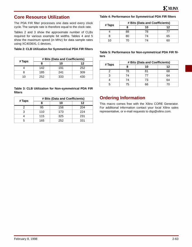
Core Resource UtilizationThe PDA FIR filter processes one data word every clockcycle. The sample rate is therefore equal to the clock rate.
Tables 2 and 3 show the approximate number of CLBsrequired for various example bit widths. Tables 4 and 5show the maximum speed (in MHz) for data sample ratesusing XC4036XL-1 devices.
Table 2: CLB Utilization for Symmetrical PDA FIR filters
Table 3: CLB Utilization for Non-symmetrical PDA FIRfilters
Table 4: Performance for Symmetrical PDA FIR filters
Table 5: Performance for Non-symmetrical PDA FIR fil-ters
Ordering InformationThis macro comes free with the Xilinx CORE Generator.For additional information contact your local Xilinx salesrepresentative, or e-mail requests to [email protected].
# Taps# Bits (Data and Coefficients)
8 10 124 142 191 2528 185 241 309
10 252 333 430
# Taps# Bits (Data and Coefficients)
8 10 122 95 156 2043 110 173 2244 115 325 2315 165 252 331
# Taps# Bits (Data and Coefficients)
8 10 124 88 78 778 80 74 65
10 70 74 60
# Taps# Bits (Data and Coefficients)
8 10 122 78 81 683 74 77 644 74 73 645 75 66 70
February 8, 1998 2-63

Parallel Distributed Arithmetic FIR FilterParallel Distributed Arithmetic FIR Filter
2-64 February 8, 1998

February 8, 1998 Product Specification
DFT Cores(Real Data In, Complex Data Out)
Xilinx Inc.2100 Logic DriveSan Jose, CA 95124Phone: +1 408-559-7778Fax: +1 408-559-7114E-mail: [email protected]: www.xilinx.com
R
DFT technology developed by Rice Electronics.
Features• 2's complement, fixed point arithmetic• Real-valued input data (15 bit)• Complex output data (16 bit ~86 dB available output
SNR)• Integrated Input Buffer (no external memory
requirements)• Transform size (N) = 32, 64, or 128 • Process real-time sampling rates >1Mhz (>12Mhz for
N=32)• Simplified interface (nominal support logic required)• Synchronous design, optimized for XC4000E, EX, and
XL families of FPGAs• Drop-in modules for the XC4000E, EX, and XL families• High performance and density guaranteed through
Relational Placed Macro (RPM) mapping and placement technology
• Available in Xilinx CORE Generator
Applications• Communications (high speed modems, transmulti-
plexers)
• Instrumentation (medical, scientific, test)• Multi-media (signal compression/decompression)• Military (radar, EW, ELINT, ESM)
General DescriptionThe 16-bit Discrete Fourier Transform (DFT) Cores arefunctionally complete elements. The designs present a sim-plified interface and require no external memory. The Corestarget the Xilinx XC4000E, EX, and XL FPGA productseries.
The Cores render the following transform for a real-valuedinput vector, f(n):
for n=0 to N-1, j=0 to (N/2-1)
where:
F(j) = output (frequency domain) coefficientsf(n) = input (time domain) sequenceN = length of input sequence (transform size)
The Cores accept a real-valued input sequence f(n) andproduce a complex output sequence F(j). Due to the real-valued nature of f(n), only the lower half of the set of F(j) isgenerated. The upper half of the F(j) is the complex conju-gate of the lower half, and therefore represents redundantinformation.
The Cores are optimized for small to medium size trans-forms (32 - 128 points). A 32-point transform can be exe-cuted in less than 5 microseconds (XC4000-3). Generalspecifications of the Cores are listed in Table 1.
F j( ) f n( )e2– πin
jN----
n 0=
N 1–
∑=
Table 1: 16-bit DFT Family Parameters
Core NameN = Size of Transform
P = Clock Periods 1 Clock Speed 2 Execution Time 3 Core Size 4
16b32pt 32 points 144 59 Mhz 2.5 usecs 274 CLBs16b64pt 64 points 1088 59 Mhz 18.5 usecs 302 CLBs16b128pt 128 points 4224 59 Mhz 71.8 usecs 394 CLBs1. P = number of clock periods for transform execution2. Preliminary maximum clock speeds based on XC4000E-1 series. Higher clock speeds are expected pending fixed layout.3. Execution Time = P/(Clock Speed in Mhz)4. XC4008 = 324 CLBs XC4010 = 400 CLBs XC4085 = 3,136 CLBs
February 8, 1998 2-65
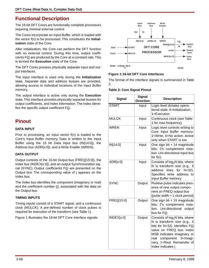
DFT Cores (Real Data In, Complex Data Out)DFT Cores (Real Data In, Complex Data Out)
Functional DescriptionThe 16-bit DFT Cores are functionally complete processorsrequiring minimal external control.
The Cores incorporate an Input Buffer, which is loaded withthe vector f(n) to be processed. This constitutes the Initial-ization state of the Core.
After initialization, the Core can perform the DFT functionwith no external control. During this time, output coeffi-cients F(j) are produced by the Core at a constant rate. Thisis termed the Execution state of the Core.
The DFT Cores possess physically separate input and out-put interfaces.
The input interface is used only during the Initializationstate. Separate data and address busses are provided,allowing access to individual locations of the Input Buffermemory.
The output interface is active only during the Executionstate. This interface provides physically separate busses foroutput coefficients, and index information. The index identi-fies the specific output coefficient F(j).
PinoutDATA INPUT
Prior to processing, an input vector f(n) is loaded to theCore's Input Buffer memory. Data is written to the InputBuffer using the 15 bit Data Input bus (IN[14:0]), theAddress bus (ADR[x:0]), and a Write Enable (WREN).
DATA OUTPUT
Output consists of the 16-bit Output bus (FREQ[15:0]), theIndex bus (INDEX[x:0]), and an output Synchronization sig-nal (SYNC). Output coefficients F(j) are presented on theOutput bus. The corresponding value of j appears on theIndex bus.
The Index bus identifies the component (imaginary or real)and the coefficient number (j), associated with the data onthe Output bus.
TIMING INPUTS
Timing inputs consist of a START signal, and a continuousclock (MULCK). A pre-defined number of clock pulses isrequired for execution of the transform (see Table 1).
Figure 1 illustrates the 16-bit DFT Core interface signals.
Figure 1:16-bit DFT Core Interfaces
The format of the interface signals is summarized in Table2.
Table 2: Core Signal Pinout
SignalSignal
DirectionDescription
START Input Logic level dictates opera-tional state: 0=Initialization, 1=Execution
MULCK Input Continuous clock (see Table 1 for max.frequency)
WREN Input Logic level controls writing toCore Input Buffer memory:1=Write, 0=No action. Activeonly when START is low
IN[14:0] Input One sign bit + 14 magnitudebits; 2's complement nota-tion. Uni-directional input busfor f(n)
ADR[x:0] Input Consists of log2N bits, whereN is transform size (e.g., 5address lines for N=32).Specifies write address toInput Buffer memory
SYNC Output Positive pulse indicates pres-ence of new output compo-nent on FREQ output bus (pulse width = 1 clock period)
FREQ[15:0] Output One sign bit + 15 magnitudebits; 2's complement nota-tion. Uni-directional outputbus for F(j)
INDEX[x:0] Output Consists of log2N bits, whereN is transform size (e.g., 5bits for N=32). Identifies F(j)value on FREQ bus. IndexMSB indicates imaginary orreal component: 0=Imagi-nary, 1=Real. Remainder ofIndex indicates j
Note: x=(log N)-12
START
MULCK
Start
Clock
DFT CORE
PROCESSOR
FREQ[15:0]
SYNC
INDEX[x:0]
IN[14:0]
InputBus
AddressBus
WriteEnable
f(n) 15
ADR[x:0] WREN
OutputBus
OutputSync.
IndexBus
X8156
F(j)
16
2-66 February 8, 1998
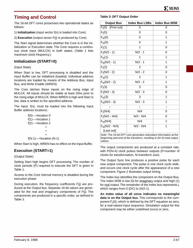
Timing and Control The 16-bit DFT cores possesses two operational states asfollows:
1) Initialization (input vector f(n) is loaded into Core)
2) Execution (output vector F(j) is produced by Core)
The Start signal determines whether the Core is in the Ini-tialization or Execution state. The Core requires a continu-ous clock input (MULCK) in both states. (Table 1 listsmaximum clock frequency.)
Initialization (START=0)(Input State)
When Start is low, DFT processing is disabled and theInput Buffer can be initialized (loaded). Individual addresslocations are loaded by means of the Address Bus, InputBus, and Write Enable (WREN).
The Core latches these inputs on the rising edge ofMULCK. All inputs should be stable at least 20ns prior tothe rising edge of MULCK. When WREN is high and Start islow, data is written to the specified address.
The input, f(n), must be loaded into the following InputBuffer address locations:
f(0)--->location 0f(1)--->location 1f(2)--->location 2
• • •
f(N-1)--->location (N-1)
When Start is high, WREN has no effect on the Input Buffer.
Execution (START=1)(Output State)
Setting Start high begins DFT processing. The number ofclock periods (P) required to execute the DFT is given inTable 1.
Access to the Core internal memory is disabled during theexecution phase.
During execution, the frequency coefficients F(j) are pro-duced at the Output bus. Separate 16 bit values are gener-ated for the real and imaginary components of F(j). Thecomponents are produced in a specific order, as defined inTable 3.
Table 3: DFT Output Order
The output components are produced at a constant rate,with P/(N+4) clock pulses between outputs (P=number ofclocks for transformation, N=transform size).
The Output Sync line produces a positive pulse for eachnew output component. The pulse is one clock cycle wide,and occurs one clock cycle after the appearance of a newcomponent. Figure 2 illustrates output timing.
The Index bus identifies the component on the Output Bus.The Index MSB is low (0) for imaginary output and high (1)for real output. The remainder of the Index bus represents j,which ranges from 0 (DC) to (N/2-1).
An Index value of all zeros indicates no meaningfuldata is on the Output bus. This corresponds to the com-ponent FI(0), which is defined by the DFT equation as zero,for a real-valued input sequence. Simulation output for thiscomponent may be either undefined (xxxx) or zero.
Output Bus Index Bus LSBs Index Bus MSBFI(0) [First out] 0 0
FI(0) 0 0
FR(0) 0 1
FR(0) 0 1
FI(1) 1 0
FI(N/2 - 1) N/2 - 1 0
FR(1) 1 1
FR(N/2 - 1) N/2 - 1 1
FI(2) 2 0
FI(N/2 - 2) N/2 - 2 0
FR(2) 2 1
FR(N/2 - 2) N/2 - 2 1
FI(3) 3 0
FI(N/2 - 3) N/2 - 3 0
FR(3) 3 1
FR(N/2 - 3) N/2 - 3 1
: : :FI(N/4) N/4 0
FI(N/2 - N/4) N/2 - N/4 0
FR(N/4) N/4 1
FR(N/2 - N/4) [Last out]
N/2 - N/4 1
Note: The 16-bit DFT core generates redundant information at the beginning and end of the transform, resulting in (N+4) total output values.
February 8, 1998 2-67
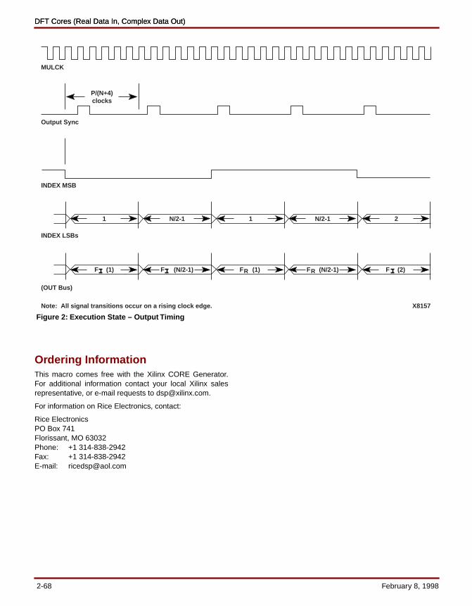
DFT Cores (Real Data In, Complex Data Out)DFT Cores (Real Data In, Complex Data Out)
Ordering InformationThis macro comes free with the Xilinx CORE Generator.For additional information contact your local Xilinx salesrepresentative, or e-mail requests to [email protected].
For information on Rice Electronics, contact:
Rice ElectronicsPO Box 741Florissant, MO 63032Phone: +1 314-838-2942Fax: +1 314-838-2942E-mail: [email protected]
MULCK
Output Sync
INDEX MSB
INDEX LSBs
P/(N+4)clocks
1 N/2-1 1 N/2-1 2
(OUT Bus)
F (1) F (N/2-1) F (2)F (1)R F (N/2-1)R
X8157Note: All signal transitions occur on a rising clock edge.
Figure 2: Execution State – Output Timing
2-68 February 8, 1998
February 8, 1998 Product Specification – PRELIMINARY
FFT Core (1024 Points)
Xilinx Inc.2100 Logic DriveSan Jose, CA 95124Phone: +1 408-559-7778Fax: +1 408-559-7114E-mail: [email protected]: www.xilinx.com
R
FFT technology developed by Rice Electronics.
Features• 2's complement, fixed-point arithmetic• Real-valued input data (15 bit)• Complex output data (16 bit ~86 dB available output
SNR)• Transform size (N) = 1024• No programming required• No "twiddle factor" memory required (internal to Core)• Process real-time sampling rates ~2Mhz• Simplified interface (nominal support logic required)• Synchronous design, optimized for XC4000E, EX, and
XL families of FPGAs• Drop-in modules for the XC4000E, EX, and XL families• High performance and density guaranteed through
Relational Placed Macro (RPM) mapping and placement technology
• Available in Xilinx CORE Generator
Applications• Communications (high speed modems, transmulti-
plexers)• Instrumentation (medical, scientific, test)• Multi-media (signal compression/decompression)• Military (radar, EW, ELINT, ESM)
General DescriptionThe 1024-point Fast Fourier Transform (FFT) Core is afunctionally complete processor. The design requires a1024-point external data memory and nominal interfacesupport. The Core targets the Xilinx XC4000E, EX, and XLFPGA product series.
The Core renders the following transform for a real-valuedinput vector, f(n):
for j=0 to (N/2-1)
where:
F(j) = output (frequency domain) coefficientsf(n) = input (time domain) sequenceN = length of input sequence (transform size)
The Core accepts a real-valued input sequence f(n) andproduces a complex output sequence F(j). Due to the real-valued nature of f(n), only the lower half of the set of F(j) isgenerated. The upper half of the F(j) is the complex conju-gate of the lower half, and therefore represents redundantinformation.
General specifications of the FFT Core are listed in Table 1.
Functional DescriptionThe 1024-point FFT Core is a functionally complete pro-cessor requiring minimal external control. Only an ExternalMemory (1k word) is required for Core operation. TheExternal Memory holds the input vector f(n) to be trans-formed.
The Core itself requires no initialization, and may be acti-vated whenever valid data is present in External Memory.When in operation, the Core must have exclusive access toExternal Memory. The Core performs "read-only" accessesto the Memory (no write operations).
F j( ) f n( )e2– πi jn
N-----------------
n 1=
N 1–
∑=
Table 1: 1024-Point FFT Parameters
Core NameN = Size of Transform
P = Clock Periods 1 Clock Speed 2 Execution Time 3 Core Size 4
1024 FFT 1024 points 17408 5321. P = number of clock periods for transform execution2. Maximum clock speed based on XC4000E-3 series3. Execution Time = P/(Clock Speed in Mhz)4. Approximately 70% utilization of F/G function generators for XC4013 device
February 8, 1998 2-69
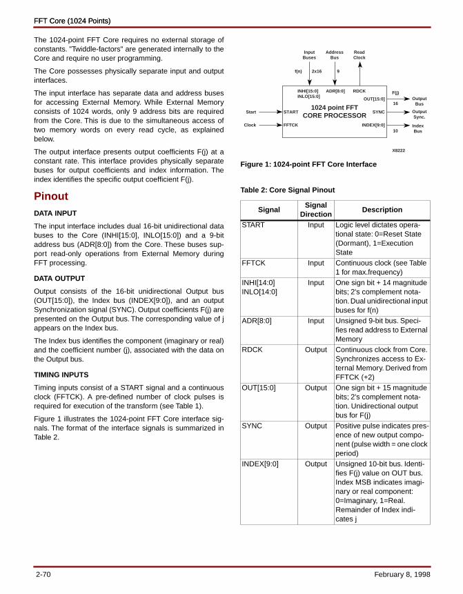
FFT Core (1024 Points)FFT Core (1024 Points)
The 1024-point FFT Core requires no external storage ofconstants. "Twiddle-factors" are generated internally to theCore and require no user programming.
The Core possesses physically separate input and outputinterfaces.
The input interface has separate data and address busesfor accessing External Memory. While External Memoryconsists of 1024 words, only 9 address bits are requiredfrom the Core. This is due to the simultaneous access oftwo memory words on every read cycle, as explainedbelow.
The output interface presents output coefficients F(j) at aconstant rate. This interface provides physically separatebuses for output coefficients and index information. Theindex identifies the specific output coefficient F(j).
PinoutDATA INPUT
The input interface includes dual 16-bit unidirectional databuses to the Core (INHI[15:0], INLO[15:0]) and a 9-bitaddress bus (ADR[8:0]) from the Core. These buses sup-port read-only operations from External Memory duringFFT processing.
DATA OUTPUT
Output consists of the 16-bit unidirectional Output bus(OUT[15:0]), the Index bus (INDEX[9:0]), and an outputSynchronization signal (SYNC). Output coefficients F(j) arepresented on the Output bus. The corresponding value of jappears on the Index bus.
The Index bus identifies the component (imaginary or real)and the coefficient number (j), associated with the data onthe Output bus.
TIMING INPUTS
Timing inputs consist of a START signal and a continuousclock (FFTCK). A pre-defined number of clock pulses isrequired for execution of the transform (see Table 1).
Figure 1 illustrates the 1024-point FFT Core interface sig-nals. The format of the interface signals is summarized inTable 2.
Figure 1: 1024-point FFT Core Interface
Table 2: Core Signal Pinout
SignalSignal
DirectionDescription
START Input Logic level dictates opera-tional state: 0=Reset State (Dormant), 1=Execution State
FFTCK Input Continuous clock (see Table 1 for max.frequency)
INHI[14:0]INLO[14:0]
Input One sign bit + 14 magnitude bits; 2's complement nota-tion. Dual unidirectional input buses for f(n)
ADR[8:0] Input Unsigned 9-bit bus. Speci-fies read address to External Memory
RDCK Output Continuous clock from Core. Synchronizes access to Ex-ternal Memory. Derived from FFTCK (+2)
OUT[15:0] Output One sign bit + 15 magnitude bits; 2's complement nota-tion. Unidirectional output bus for F(j)
SYNC Output Positive pulse indicates pres-ence of new output compo-nent (pulse width = one clock period)
INDEX[9:0] Output Unsigned 10-bit bus. Identi-fies F(j) value on OUT bus. Index MSB indicates imagi-nary or real component: 0=Imaginary, 1=Real. Remainder of Index indi-cates j
START
FFTCK
Start
Clock
1024 point FFT CORE PROCESSOR
OUT[15:0]
SYNC
INDEX[9:0]
INHI[15:0]INLO[15:0]
InputBuses
AddressBus
ReadClock
f(n) 2x16
ADR[8:0] RDCK
OutputBus
OutputSync.
IndexBus
X8222
F(j)
16
9
10
2-70 February 8, 1998
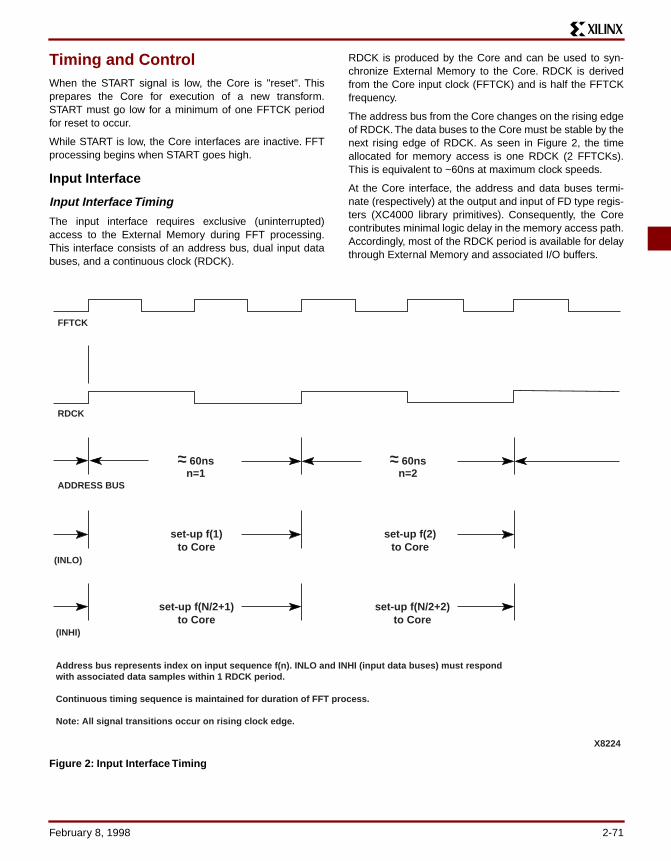
Timing and Control When the START signal is low, the Core is "reset". Thisprepares the Core for execution of a new transform.START must go low for a minimum of one FFTCK periodfor reset to occur.
While START is low, the Core interfaces are inactive. FFTprocessing begins when START goes high.
Input Interface
Input Interface Timing
The input interface requires exclusive (uninterrupted)access to the External Memory during FFT processing.This interface consists of an address bus, dual input databuses, and a continuous clock (RDCK).
RDCK is produced by the Core and can be used to syn-chronize External Memory to the Core. RDCK is derivedfrom the Core input clock (FFTCK) and is half the FFTCKfrequency.
The address bus from the Core changes on the rising edgeof RDCK. The data buses to the Core must be stable by thenext rising edge of RDCK. As seen in Figure 2, the timeallocated for memory access is one RDCK (2 FFTCKs).This is equivalent to ~60ns at maximum clock speeds.
At the Core interface, the address and data buses termi-nate (respectively) at the output and input of FD type regis-ters (XC4000 library primitives). Consequently, the Corecontributes minimal logic delay in the memory access path.Accordingly, most of the RDCK period is available for delaythrough External Memory and associated I/O buffers.
FFTCK
RDCK
ADDRESS BUS
X8224
Address bus represents index on input sequence f(n). INLO and INHI (input data buses) must respondwith associated data samples within 1 RDCK period.
Continuous timing sequence is maintained for duration of FFT process.
Note: All signal transitions occur on rising clock edge.
(INLO)
(INHI)
~~ 60nsn=1
~~ 60nsn=2
set-up f(1)to Core
set-up f(2)to Core
set-up f(N/2+1)to Core
set-up f(N/2+2)to Core
Figure 2: Input Interface Timing
February 8, 1998 2-71
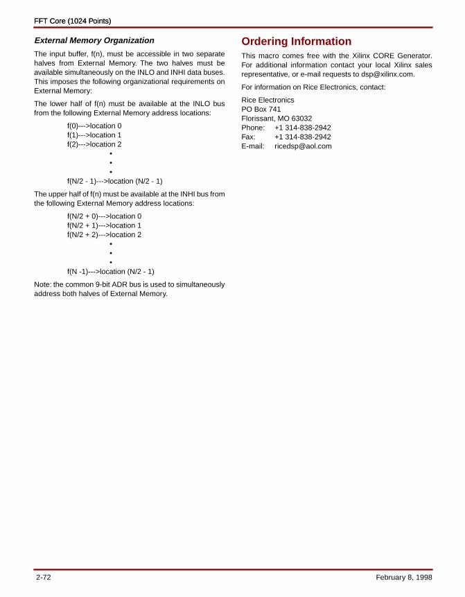
FFT Core (1024 Points)FFT Core (1024 Points)
External Memory Organization
The input buffer, f(n), must be accessible in two separatehalves from External Memory. The two halves must beavailable simultaneously on the INLO and INHI data buses.This imposes the following organizational requirements onExternal Memory:
The lower half of f(n) must be available at the INLO busfrom the following External Memory address locations:
f(0)--->location 0f(1)--->location 1f(2)--->location 2
• • •
f(N/2 - 1)--->location (N/2 - 1)
The upper half of f(n) must be available at the INHI bus fromthe following External Memory address locations:
f(N/2 + 0)--->location 0f(N/2 + 1)--->location 1f(N/2 + 2)--->location 2
• • •
f(N -1)--->location (N/2 - 1)
Note: the common 9-bit ADR bus is used to simultaneouslyaddress both halves of External Memory.
Ordering InformationThis macro comes free with the Xilinx CORE Generator.For additional information contact your local Xilinx salesrepresentative, or e-mail requests to [email protected].
For information on Rice Electronics, contact:
Rice ElectronicsPO Box 741Florissant, MO 63032Phone: +1 314-838-2942Fax: +1 314-838-2942E-mail: [email protected]
2-72 February 8, 1998

SDA FIR Control Logic
February 8, 1998 Product Specification
Xilinx Inc.2100 Logic DriveSan Jose, CA 95124Phone: +1 408-559-7778Fax: +1 408-559-7114E-mail: [email protected]: www.xilinx.com
R
Features• Drop-in modules for the XC4000E, EX, and XL families• High performance and density guaranteed through
Relational Placed Macro (RPM) mapping and placement technology
• Available in Xilinx CORE Generator
Functional DescriptionThis macro accepts a bit serial processing clock input, adata-sync (DSYNC), and a data-width signal (TC) on theinput pins to control a Serial Distributed Arithmetic (SDA)process. The DSYNC input is used to start the bit serialprocess by signaling that a new data sample has arrived forprocessing. The internal control logic will start countingfrom 0 to a TC equal to N-2 for N-bit data to produce theoutputs TSBTC, MSBTC, and HOLD. The DSYNC input isused to trigger the LSB of the SDA process. TSBTC resetsthe time-skew buffer and MSBTC disables the macros onthe MSB of the SDA process until a new data sample is reg-istered. The process is then repeated.
PinoutSignal names for the schematic symbol are shown in Fig-ure 1 and described in Table 1.
Figure 1: Core Schematic Symbol
Table 1: Core Signal Pinout
SignalSignal
DirectionDescription
CLK Input BIT-PROCESSING CLOCK – clocks the SDA bit serial process. Must have a fre-quency of N+1 times or greater than the data clock for N-bit data.
DSYNC Input DATA SAMPLE READY IN-PUT – DSYNC is used to re-set the Control Logic to begin processing the next data sample. When DSYNC is as-serted (HIGH), the input data is registered on the next ris-ing edge of the C (CLOCK). This data is fed into the par-allel-to-serial converter and the DSYNC is propagated through the data flow to trig-ger the LSB input of each cascaded stage of the SDA process. The active duration of DSYNC must be equal to one period, from rising-edge to rising-edge, of the bit pro-cessing clock and remain in-active for at least N clock cycles of the bit processing clock for N-bit data.
SDACL16
X7556
DSYNC
CLK
HOLDTC[3:0]
MSBTC
TSBTC
February 8, 1998 2-73
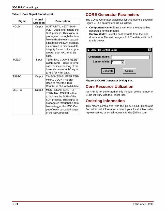
SDA FIR Control LogicSDA FIR Control Logic
Table 1: Core Signal Pinout (cont.) CORE Generator ParametersThe CORE Generator dialog box for this macro is shown inFigure 2. The parameters are as follows:
• Component Name : Enter a name for the output files generated for this module.
• Control Width : Select a control width from the pull-down menu. The valid range is 2-5. The data width is 2 to this power.
Figure 2: CORE Generator Dialog Box
Core Resource UtilizationAn RPM is not generated for this module, so the number ofCLBs will vary with the Placer tool.
Ordering InformationThis macro comes free with the Xilinx CORE Generator.For additional information contact your local Xilinx salesrepresentative, or e-mail requests to [email protected].
SignalSignal
DirectionDescription
HOLD Output WAIT UNTIL NEXT SAM-PLE – Used to terminate the SDA process. This signal is propagated through the data flow to disable each cascad-ed stage of the SDA process, as required to maintain data integrity for each clock cycle greater than N+1 for N-bit data.
TC[3:0] Input TERMINAL COUNT RESET CONSTANT – Used to termi-nate the incrementing of the internal counter at TC equal to N-2 for N-bit data.
TSBTC Output TIME-SKEW-BUFFER TER-MINAL COUNT RESET – Used to reset the TSB Counter at N-1 for N-bit data.
MSBTC Output MOST SIGNIFICANT BIT TERMINAL COUNT – Used to indicate the MSB of the SDA process. This signal is propagated through the data flow to trigger the MSB Out-put of each cascaded stage of the SDA process.
2-74 February 8, 1998

Sine/Cosine
February 8, 1998 Product Specification
Xilinx Inc.2100 Logic DriveSan Jose, CA 95124Phone: +1 408-559-7778Fax: +1 408-559-7114E-mail: [email protected]: www.xilinx.com
R
Features• Fully parameterizable sin/cos look-up table• Input address widths from 3 to 10 bits• Output data widths from 4 to 16 bits• User can determine the accuracy of the result by
selecting the desired output width• Utilizes fast internal XC4000 distributed ROM• Easy to use: any table size and output resolution can be
specified• Efficient: calculates full 360 degree table from 90
degree segment• Useful in high-speed modulation/demodulation
applications• Drop-in modules for the XC4000E, EX, and XL families• High performance and density guaranteed through
Relational Placed Macro (RPM) mapping and placement technology
• Available in Xilinx CORE Generator
Functional DescriptionThe Sine/Cosine module returns the value sin(theta) whenthe control input is High and the value cos(theta) when thecontrol input is Low.
The module contains an internal ROM look-up table thatstores only the values for the first quarter of the sine wave.Values of sin(theta) or cos(theta) are derived from thisstored data by appropriate negations of an input theta andthe value fetched from the internal table. The decisions tonegate are based on the state of the two most significantbits of theta and the Ctrl input.
PinoutSignal names for the schematic symbol are shown in Fig-ure 1 and described in Table 1.
Figure 1: Block Diagram
Table 1: Core Signal Pinout
CORE Generator ParametersThe CORE Generator accepts the parameters enteredthrough the dialog box and creates the specific design fromthe values entered using a parameterized VHDL recipe.VHDL instantiation code and a schematic symbol are cre-ated along with the netlist for the design.
The CORE Generator dialog box for this macro is shown inFigure 2. The parameters are as follows:
• Component Name : Enter a name for the component.• Address Width : Select the width of the theta input bus.
The valid range is 3 to 10. This value is also used to specify the depth of the required look-up table. The number of sample data points in the look-up table is 2 to the Address Width power.
SignalSignal
DirectionDescription
Theta Input Input valueCtrl Input Control – when high, returns
the sine of theta; when low, returns the cosine
C Input Clock – active on rising edgeOutput Output Output value – the sine or
cosine of theta
OutputTheta
Ctrl
Sine/Cosine
CClock
X8140
February 8, 1998 2-75
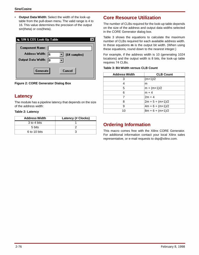
Sine/CosineSine/Cosine
• Output Data Width : Select the width of the look-up table from the pull-down menu. The valid range is 4 to 16. This value determines the precision of the output sin(theta) or cos(theta).
Figure 2: CORE Generator Dialog Box
LatencyThe module has a pipeline latency that depends on the sizeof the address width:
Table 2: Latency
Core Resource UtilizationThe number of CLBs required for the look-up table dependson the size of the address and output data widths selectedin the CORE Generator dialog box.
Table 3 shows the equations to calculate the maximumnumber of CLBs required for each available address width.In these equations m is the output bit width. (When usingthese equations, round down to the nearest integer.)
For example, if the address width is 10 (generating 1024locations) and the output width is 8 bits, the look-up tablerequires 74 CLBs.
Table 3: Bit Width versus CLB Count
Ordering InformationThis macro comes free with the Xilinx CORE Generator.For additional information contact your local Xilinx salesrepresentative, or e-mail requests to [email protected].
Address Width Latency (# Clocks)3 to 4 bits 1
5 bits 26 to 10 bits 3
Address Width CLB Count3 (m+1)/2 4 m 5 m + (m+1)/2 6 m + 4 7 2m + 4 8 2m + 5 + (m+1)/2 9 4m + 6 + (m+1)/2
10 8m + 6 + (m+1)/2
2-76 February 8, 1998

Non-Symmetric, 16-Deep Time Skew Buffer
February 8, 1998 Product Specification
Xilinx Inc.2100 Logic DriveSan Jose, CA 95124Phone: +1 408-559-7778Fax: +1 408-559-7114E-mail: [email protected]: www.xilinx.com
R
Features• Drop-in modules for the XC4000E, EX, and XL families• High performance and density guaranteed through
Relational Placed Macro (RPM) mapping and placement technology
• Available in Xilinx CORE Generator
Functional DescriptionThis macro accepts a serial data input on the SDI pin. Thisdata is stored in a series of Serially Cascaded, 16-bit Syn-chronous RAM-based shift registers. The RAM’s outputdata is registered and presented on the Q pins of theMacro. Each register’s Q pin is internally cascaded to thefollowing RAM’s Data Input. The 16-bit RAM-based shiftregister supports 1- to 16-bit wide data storage per stage.The RESET pin is used to control the Bit-Width of theserial-data to be stored via the control logic.
The RAM address is controlled via an internal, free-run-ning, 16-bit counter (CNT04RE). The counter is controlledby the CE (active high) and RESET inputs. The CNT04REgenerates an output, 0 to TC, where TC is controlled via theRESET signal from the Control Logic, SDACL16. Theaddressing sequence of the cascaded registered RAM isstructured to increment the address of each data-bit byone. That is, the bit-n is stored at an address ADDR+1 foreach consecutive RAM. This is because each data sampleis registered prior to writing it into the following cascadedRAM. The registration of the RAM data is important tomaintain a synchronous system, as the RAM is synchro-nous write and asynchronous read. Hence, the RAM dataoutput will change, to represent the data stored at a given
address, as the address changes. The Truth Table for thisfunction is shown in Table 1.
Table 1: Truth Table
PinoutSignal names for the schematic symbol are shown in Fig-ure 1 and Table 2.
Figure 1: Core Schematic Diagram
WE(mode) Data CE TC C CNT Q[N-1,0]
X X 0 X X No Change
No Change
0 (read) X 1 CNT<TC+1 1/4 CNT+1 Data@CNT
1 (write) Data 1 CNT<TC+1 1/4 CNT+1 Data@CNT
0 (read) X 1 CNT=TC+1 1/4 0 Data@CNT
1 (write) Data 1 CNT=TC+1 1/4 0 Data@CNT
TSB16xXX
X7555
SDI
WE
RESET
CE
C
Q1
Q0
February 8, 1998 2-77
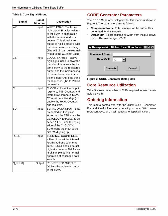
Non-Symmetric, 16-Deep Time Skew BufferNon-Symmetric, 16-Deep Time Skew Buffer
Table 2: Core Signal Pinout CORE Generator ParametersThe CORE Generator dialog box for this macro is shown inFigure 2. The parameters are as follows:
• Component Name : Enter a name for the output files generated for this module.
• Data Width : Select an input bit width from the pull-down menu. The valid range is 2-32.
Figure 2: CORE Generator Dialog Box
Core Resource UtilizationTable 3 shows the number of CLBs required for each avail-able bit width.
Ordering InformationThis macro comes free with the Xilinx CORE Generator.For additional information contact your local Xilinx salesrepresentative, or e-mail requests to [email protected].
SignalSignal
DirectionDescription
WE Input WRITE ENABLE – Active high signal, Enables writing to the RAM in association with the internal address counter. This signal is re-quired to hold a block a data for consecutive processing. (The WE pin can be external-ly tied to the CE if not used.)
CE Input CLOCK ENABLE – active high signal used to allow the transfer of data from the in-ternal RAM to the registered output and the incrementing of the Address used to con-trol the TSB RAM data trans-fer sequence. (Tie to VCC if not used.)
C Input CLOCK – clocks the output registers, TSB Counter, and internal synchronous RAM. CE must be active (high) to enable the RAM, Counter, and registers.
SDI Input SERIAL DATA INPUT – data presented on this pin is stored into the TSB when the CE (CLOCK ENABLE) is as-serted (HIGH) and the rising edge of the C (CLOCK). SDI0 feeds the Input to the first RAM going up.
RESET Input TERMINAL COUNT RESET – Used to reset the internal RAM’s address counter to zero. RESET should be set high at a count of N-2 for an N-bit sample during normal operation of cascaded data-sample.
Q[N-1, 0] Output REGISTERED OUTPUT DATA – the registered output of the RAM.
2-78 February 8, 1998
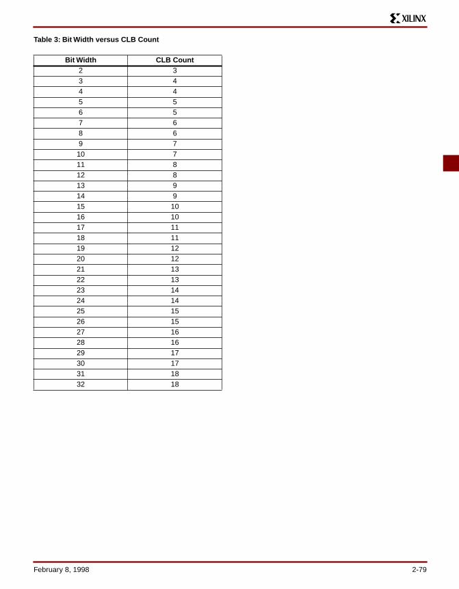
Table 3: Bit Width versus CLB Count
Bit Width CLB Count2 33 44 45 56 57 68 69 7
10 711 812 813 914 915 1016 1017 1118 1119 1220 1221 1322 1323 1424 1425 1526 1527 1628 1629 1730 1731 1832 18
February 8, 1998 2-79

Non-Symmetric, 16-Deep Time Skew BufferNon-Symmetric, 16-Deep Time Skew Buffer
2-80 February 8, 1998
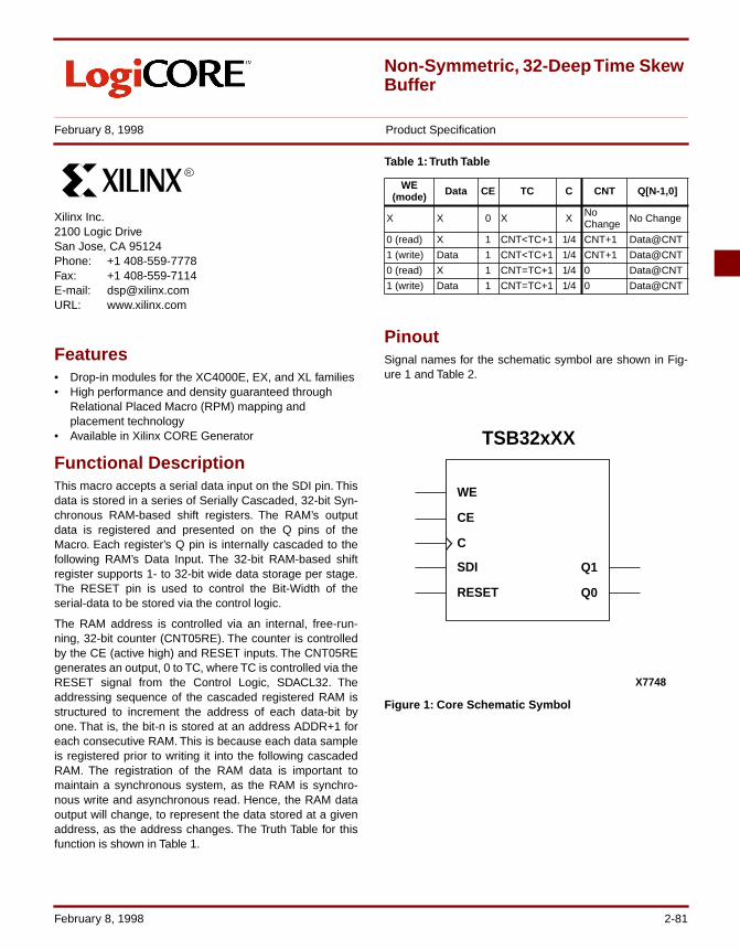
Non-Symmetric, 32-Deep Time Skew Buffer
February 8, 1998 Product Specification
Xilinx Inc.2100 Logic DriveSan Jose, CA 95124Phone: +1 408-559-7778Fax: +1 408-559-7114E-mail: [email protected]: www.xilinx.com
R
Features• Drop-in modules for the XC4000E, EX, and XL families• High performance and density guaranteed through
Relational Placed Macro (RPM) mapping and placement technology
• Available in Xilinx CORE Generator
Functional DescriptionThis macro accepts a serial data input on the SDI pin. Thisdata is stored in a series of Serially Cascaded, 32-bit Syn-chronous RAM-based shift registers. The RAM’s outputdata is registered and presented on the Q pins of theMacro. Each register’s Q pin is internally cascaded to thefollowing RAM’s Data Input. The 32-bit RAM-based shiftregister supports 1- to 32-bit wide data storage per stage.The RESET pin is used to control the Bit-Width of theserial-data to be stored via the control logic.
The RAM address is controlled via an internal, free-run-ning, 32-bit counter (CNT05RE). The counter is controlledby the CE (active high) and RESET inputs. The CNT05REgenerates an output, 0 to TC, where TC is controlled via theRESET signal from the Control Logic, SDACL32. Theaddressing sequence of the cascaded registered RAM isstructured to increment the address of each data-bit byone. That is, the bit-n is stored at an address ADDR+1 foreach consecutive RAM. This is because each data sampleis registered prior to writing it into the following cascadedRAM. The registration of the RAM data is important tomaintain a synchronous system, as the RAM is synchro-nous write and asynchronous read. Hence, the RAM dataoutput will change, to represent the data stored at a givenaddress, as the address changes. The Truth Table for thisfunction is shown in Table 1.
Table 1: Truth Table
PinoutSignal names for the schematic symbol are shown in Fig-ure 1 and Table 2.
Figure 1: Core Schematic Symbol
WE(mode) Data CE TC C CNT Q[N-1,0]
X X 0 X X No Change No Change
0 (read) X 1 CNT<TC+1 1/4 CNT+1 Data@CNT
1 (write) Data 1 CNT<TC+1 1/4 CNT+1 Data@CNT
0 (read) X 1 CNT=TC+1 1/4 0 Data@CNT
1 (write) Data 1 CNT=TC+1 1/4 0 Data@CNT
TSB32xXX
X7748
SDI
WE
RESET
CE
C
Q1
Q0
February 8, 1998 2-81
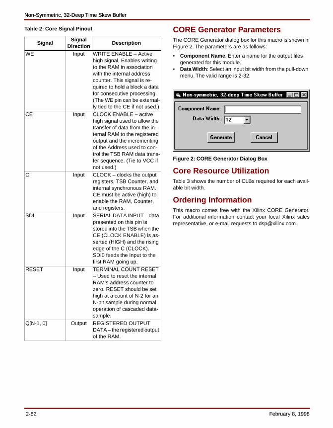
Non-Symmetric, 32-Deep Time Skew BufferNon-Symmetric, 32-Deep Time Skew Buffer
Table 2: Core Signal Pinout CORE Generator ParametersThe CORE Generator dialog box for this macro is shown inFigure 2. The parameters are as follows:
• Component Name : Enter a name for the output files generated for this module.
• Data Width : Select an input bit width from the pull-down menu. The valid range is 2-32.
Figure 2: CORE Generator Dialog Box
Core Resource UtilizationTable 3 shows the number of CLBs required for each avail-able bit width.
Ordering InformationThis macro comes free with the Xilinx CORE Generator.For additional information contact your local Xilinx salesrepresentative, or e-mail requests to [email protected].
SignalSignal
DirectionDescription
WE Input WRITE ENABLE – Active high signal, Enables writing to the RAM in association with the internal address counter. This signal is re-quired to hold a block a data for consecutive processing. (The WE pin can be external-ly tied to the CE if not used.)
CE Input CLOCK ENABLE – active high signal used to allow the transfer of data from the in-ternal RAM to the registered output and the incrementing of the Address used to con-trol the TSB RAM data trans-fer sequence. (Tie to VCC if not used.)
C Input CLOCK – clocks the output registers, TSB Counter, and internal synchronous RAM. CE must be active (high) to enable the RAM, Counter, and registers.
SDI Input SERIAL DATA INPUT – data presented on this pin is stored into the TSB when the CE (CLOCK ENABLE) is as-serted (HIGH) and the rising edge of the C (CLOCK). SDI0 feeds the Input to the first RAM going up.
RESET Input TERMINAL COUNT RESET – Used to reset the internal RAM’s address counter to zero. RESET should be set high at a count of N-2 for an N-bit sample during normal operation of cascaded data-sample.
Q[N-1, 0] Output REGISTERED OUTPUT DATA – the registered output of the RAM.
2-82 February 8, 1998
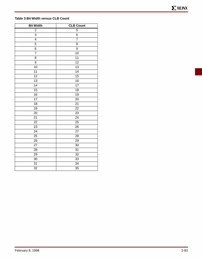
Table 3:Bit Width versus CLB Count
Bit Width CLB Count2 53 64 75 86 97 108 119 12
10 1311 1412 1513 1614 1715 1816 1917 2018 2119 2220 2321 2422 2523 2624 2725 2826 2927 3028 3129 3230 3331 3432 35
February 8, 1998 2-83

Non-Symmetric, 32-Deep Time Skew BufferNon-Symmetric, 32-Deep Time Skew Buffer
2-84 February 8, 1998
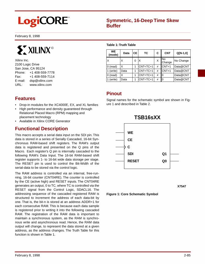
Symmetric, 16-Deep Time Skew Buffer
February 8, 1998
Xilinx Inc.2100 Logic DriveSan Jose, CA 95124Phone: +1 408-559-7778Fax: +1 408-559-7114E-mail: [email protected]: www.xilinx.com
R
Features• Drop-in modules for the XC4000E, EX, and XL families• High performance and density guaranteed through
Relational Placed Macro (RPM) mapping and placement technology
• Available in Xilinx CORE Generator
Functional DescriptionThis macro accepts a serial data input on the SDI pin. Thisdata is stored in a series of Serially Cascaded, 16-bit Syn-chronous RAM-based shift registers. The RAM’s outputdata is registered and presented on the Q pins of theMacro. Each register’s Q pin is internally cascaded to thefollowing RAM’s Data Input. The 16-bit RAM-based shiftregister supports 1- to 16-bit wide data storage per stage.The RESET pin is used to control the Bit-Width of theserial-data to be stored via the control logic.
The RAM address is controlled via an internal, free-run-ning, 16-bit counter (CNT04RE). The counter is controlledby the CE (active high) and RESET inputs. The CNT04REgenerates an output, 0 to TC, where TC is controlled via theRESET signal from the Control Logic, SDACL16. Theaddressing sequence of the cascaded registered RAM isstructured to increment the address of each data-bit byone. That is, the bit-n is stored at an address ADDR+1 foreach consecutive RAM. This is because each data sampleis registered prior to writing it into the following cascadedRAM. The registration of the RAM data is important tomaintain a synchronous system, as the RAM is synchro-nous write and asynchronous read. Hence, the RAM dataoutput will change, to represent the data stored at a givenaddress, as the address changes. The Truth Table for thisfunction is shown in Table 1.
Table 1: Truth Table
PinoutSignal names for the schematic symbol are shown in Fig-ure 1 and described in Table 2.
Figure 1: Core Schematic Symbol
WE(mode) Data CE TC C CNT Q[N-1,0]
X X 0 X X No Change No Change
0 (read) X 1 CNT<TC+1 ≠ CNT+1 Data@CNT
1 (write) Data 1 CNT<TC+1 ≠ CNT+1 Data@CNT
0 (read) X 1 CNT=TC+1 ≠ 0 Data@CNT
1 (write) Data 1 CNT=TC+1 ≠ 0 Data@CNT
TSB16sXX
X7547
SDI
WE
RESET
CE
C
Q1
Q0
February 8, 1998 2-85
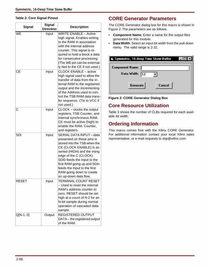
Symmetric, 16-Deep Time Skew BufferSymmetric, 16-Deep Time Skew Buffer
Table 2: Core Signal Pinout CORE Generator ParametersThe CORE Generator dialog box for this macro is shown inFigure 2. The parameters are as follows.
• Component Name : Enter a name for the output files generated for this module.
• Data Width : Select an input bit width from the pull-down menu. The valid range is 2-32.
Figure 2: CORE Generator Dialog Box
Core Resource UtilizationTable 3 shows the number of CLBs required for each avail-able bit width.
Ordering InformationThis macro comes free with the Xilinx CORE Generator.For additional information contact your local Xilinx salesrepresentative, or e-mail requests to [email protected].
SignalSignal
DirectionDescription
WE Input WRITE ENABLE – Active high signal, Enables writing to the RAM in association with the internal address counter. This signal is re-quired to hold a block a data for consecutive processing. (The WE pin can be external-ly tied to the CE if not used.)
CE Input CLOCK ENABLE – active high signal used to allow the transfer of data from the in-ternal RAM to the registered output and the incrementing of the Address used to con-trol the TSB RAM data trans-fer sequence. (Tie to VCC if not used.)
C Input CLOCK – clocks the output registers, TSB Counter, and internal synchronous RAM. CE must be active (high) to enable the RAM, Counter, and registers.
SDI Input SERIAL DATA INPUT – data presented on these pins is stored into the TSB when the CE (CLOCK ENABLE) is as-serted (HIGH) and the rising edge of the C (CLOCK). SDI0 feeds the Input to the first RAM going up and SDIn feeds the Input to the first RAM going down to create an up-down data flow.
RESET Input TERMINAL COUNT RESET – Used to reset the internal RAM’s address counter to zero. RESET should be set high at a count of N-2 for an N-bit sample during normal operation of cascaded data-sample.
Q[N-1, 0] Output REGISTERED OUTPUT DATA – the registered output of the RAM.
2-86
Table 3: Bit Width versus CLB Count
Bit Width CLB Count2 33 44 45 56 57 68 69 7
10 711 812 813 914 915 1016 1017 1118 1119 1220 1221 1322 1323 1424 1425 1526 1527 1628 1629 1730 1731 1832 18
2-87

Symmetric, 16-Deep Time Skew BufferSymmetric, 16-Deep Time Skew Buffer
2-88
Base-Level Functions Table of Contents
February 8, 1998
Basic ElementsConstant . . . . . . . . . . . . . . . . . . . . . . . . . . . . . . . . . . . . . . . . . . . . . . . . . . . . . . . . .2-91Two Input MUX . . . . . . . . . . . . . . . . . . . . . . . . . . . . . . . . . . . . . . . . . . . . . . . . . . .2-93Three Input MUX . . . . . . . . . . . . . . . . . . . . . . . . . . . . . . . . . . . . . . . . . . . . . . . . . .2-95Four Input MUX . . . . . . . . . . . . . . . . . . . . . . . . . . . . . . . . . . . . . . . . . . . . . . . . . . .2-97Parallel to Serial Converter . . . . . . . . . . . . . . . . . . . . . . . . . . . . . . . . . . . . . . . . . .2-99Register . . . . . . . . . . . . . . . . . . . . . . . . . . . . . . . . . . . . . . . . . . . . . . . . . . . . . . . .2-101Math Functions1’s and 2’s Complement . . . . . . . . . . . . . . . . . . . . . . . . . . . . . . . . . . . . . . . . . . . .2-103Scaled By 1/2 Accumulator . . . . . . . . . . . . . . . . . . . . . . . . . . . . . . . . . . . . . . . . .2-105Registered Adder . . . . . . . . . . . . . . . . . . . . . . . . . . . . . . . . . . . . . . . . . . . . . . . . .2-107Registered Loadable Adder . . . . . . . . . . . . . . . . . . . . . . . . . . . . . . . . . . . . . . . . .2-109Registered Scaled Adder . . . . . . . . . . . . . . . . . . . . . . . . . . . . . . . . . . . . . . . . . . 2-111Registered Serial Adder . . . . . . . . . . . . . . . . . . . . . . . . . . . . . . . . . . . . . . . . . . . 2-113Integrator . . . . . . . . . . . . . . . . . . . . . . . . . . . . . . . . . . . . . . . . . . . . . . . . . . . . . . .2-115Constant Coefficient Multiplier . . . . . . . . . . . . . . . . . . . . . . . . . . . . . . . . . . . . . . .2-117Constant Coefficient Multiplier (Pipelined) . . . . . . . . . . . . . . . . . . . . . . . . . . . . . 2-119Parallel Multipliers - Area Optimized. . . . . . . . . . . . . . . . . . . . . . . . . . . . . . . . . . 2-121Parallel Multipliers - Performance Optimized . . . . . . . . . . . . . . . . . . . . . . . . . . . 2-125Square Root . . . . . . . . . . . . . . . . . . . . . . . . . . . . . . . . . . . . . . . . . . . . . . . . . . . . .2-127Registered Subtracter . . . . . . . . . . . . . . . . . . . . . . . . . . . . . . . . . . . . . . . . . . . . . 2-129Registered Loadable Subtracter . . . . . . . . . . . . . . . . . . . . . . . . . . . . . . . . . . . . . 2-131MemoriesDelay Element . . . . . . . . . . . . . . . . . . . . . . . . . . . . . . . . . . . . . . . . . . . . . . . . . . .2-133Synchronous FIFO . . . . . . . . . . . . . . . . . . . . . . . . . . . . . . . . . . . . . . . . . . . . . . . .2-13516-Word Deep Registered Look-Up Table . . . . . . . . . . . . . . . . . . . . . . . . . . . . . 2-13932-Word Deep Registered Look-Up Table . . . . . . . . . . . . . . . . . . . . . . . . . . . . . 2-141Registered Synchronous RAM . . . . . . . . . . . . . . . . . . . . . . . . . . . . . . . . . . . . . . 2-143Registered ROM . . . . . . . . . . . . . . . . . . . . . . . . . . . . . . . . . . . . . . . . . . . . . . . . .2-145
February 8, 1998 2-89

Base-Level Functions Table of Contents
2-90 February 8, 1998
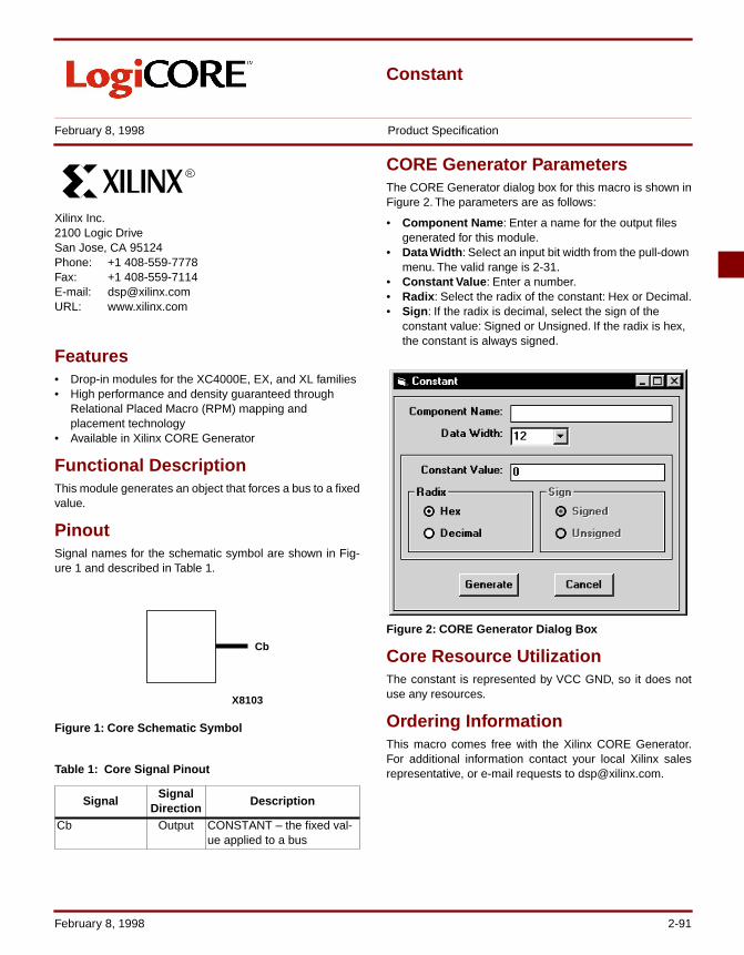
Constant
February 8, 1998 Product Specification
Xilinx Inc.2100 Logic DriveSan Jose, CA 95124Phone: +1 408-559-7778Fax: +1 408-559-7114E-mail: [email protected]: www.xilinx.com
R
Features• Drop-in modules for the XC4000E, EX, and XL families• High performance and density guaranteed through
Relational Placed Macro (RPM) mapping and placement technology
• Available in Xilinx CORE Generator
Functional DescriptionThis module generates an object that forces a bus to a fixedvalue.
PinoutSignal names for the schematic symbol are shown in Fig-ure 1 and described in Table 1.
Figure 1: Core Schematic Symbol
Table 1: Core Signal Pinout
CORE Generator ParametersThe CORE Generator dialog box for this macro is shown inFigure 2. The parameters are as follows:
• Component Name : Enter a name for the output files generated for this module.
• Data Width : Select an input bit width from the pull-down menu. The valid range is 2-31.
• Constant Value : Enter a number.• Radix : Select the radix of the constant: Hex or Decimal.• Sign : If the radix is decimal, select the sign of the
constant value: Signed or Unsigned. If the radix is hex, the constant is always signed.
Figure 2: CORE Generator Dialog Box
Core Resource UtilizationThe constant is represented by VCC GND, so it does notuse any resources.
Ordering InformationThis macro comes free with the Xilinx CORE Generator.For additional information contact your local Xilinx salesrepresentative, or e-mail requests to [email protected].
SignalSignal
DirectionDescription
Cb Output CONSTANT – the fixed val-ue applied to a bus
Cb
X8103
February 8, 1998 2-91

ConstantConstant
2-92 February 8, 1998
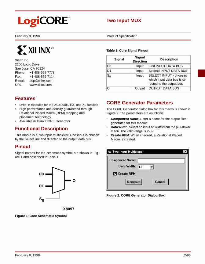
Two Input MUX
February 8, 1998 Product Specification
Xilinx Inc.2100 Logic DriveSan Jose, CA 95124Phone: +1 408-559-7778Fax: +1 408-559-7114E-mail: [email protected]: www.xilinx.com
R
Features• Drop-in modules for the XC4000E, EX, and XL families• High performance and density guaranteed through
Relational Placed Macro (RPM) mapping and placement technology
• Available in Xilinx CORE Generator
Functional DescriptionThis macro is a two-input multiplexer. One input is chosenby the Select line and directed to the output data bus.
PinoutSignal names for the schematic symbol are shown in Fig-ure 1 and described in Table 1.
Figure 1: Core Schematic Symbol
Table 1: Core Signal Pinout
CORE Generator ParametersThe CORE Generator dialog box for this macro is shown inFigure 2. The parameters are as follows:
• Component Name : Enter a name for the output files generated for this module.
• Data Width : Select an input bit width from the pull-down menu. The valid range is 2-32.
• Create RPM : When checked, a Relational Placed Macro is created.
Figure 2: CORE Generator Dialog Box
O
D0
X8097
S
D1
0
Signal Signal
DirectionDescription
D0 Input First INPUT DATA BUSD1 Input Second INPUT DATA BUSS0 Input SELECT INPUT - chooses
which input data bus is di-rected to the output bus
O Output OUTPUT DATA BUS
February 8, 1998 2-93
Two Input MUXTwo Input MUX
Core Resource UtilizationTable 2 shows the number of CLBs required for each avail-able bit width.
Table 2: Bit Width versus CLB Count
Ordering InformationThis macro comes free with the Xilinx CORE Generator.For additional information contact your local Xilinx salesrepresentative, or e-mail requests to [email protected].
Bit Width CLB Count2 13 24 25 36 37 48 49 5
10 511 612 613 714 715 816 817 918 919 1020 1021 1122 1123 1224 1225 1326 1327 1428 1429 1530 1531 1632 16
2-94 February 8, 1998
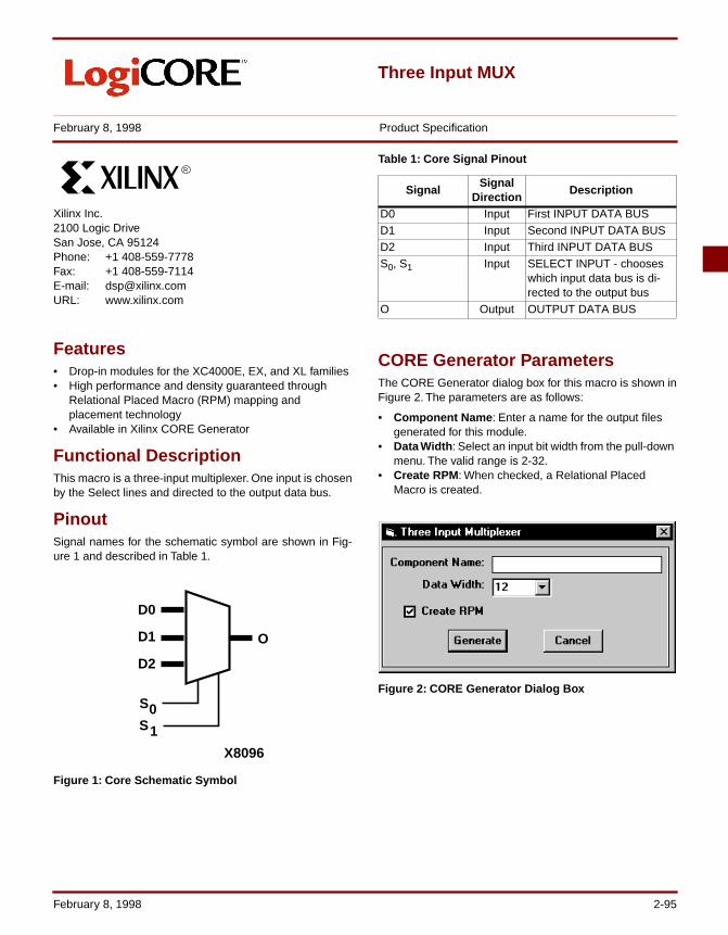
Three Input MUX
February 8, 1998 Product Specification
Xilinx Inc.2100 Logic DriveSan Jose, CA 95124Phone: +1 408-559-7778Fax: +1 408-559-7114E-mail: [email protected]: www.xilinx.com
R
Features• Drop-in modules for the XC4000E, EX, and XL families• High performance and density guaranteed through
Relational Placed Macro (RPM) mapping and placement technology
• Available in Xilinx CORE Generator
Functional DescriptionThis macro is a three-input multiplexer. One input is chosenby the Select lines and directed to the output data bus.
PinoutSignal names for the schematic symbol are shown in Fig-ure 1 and described in Table 1.
Figure 1: Core Schematic Symbol
Table 1: Core Signal Pinout
CORE Generator ParametersThe CORE Generator dialog box for this macro is shown inFigure 2. The parameters are as follows:
• Component Name : Enter a name for the output files generated for this module.
• Data Width : Select an input bit width from the pull-down menu. The valid range is 2-32.
• Create RPM : When checked, a Relational Placed Macro is created.
Figure 2: CORE Generator Dialog Box
OD1
D0
X8096
S
D2
S0
1
Signal Signal
DirectionDescription
D0 Input First INPUT DATA BUSD1 Input Second INPUT DATA BUSD2 Input Third INPUT DATA BUSS0, S1 Input SELECT INPUT - chooses
which input data bus is di-rected to the output bus
O Output OUTPUT DATA BUS
February 8, 1998 2-95

Three Input MUXThree Input MUX
Core Resource UtilizationTable 2 shows the number of CLBs required for each avail-able bit width.
Table 2:Bit Width versus CLB Count
Ordering InformationThis macro comes free with the Xilinx CORE Generator.For additional information contact your local Xilinx salesrepresentative, or e-mail requests to [email protected].
Bit Width CLB Count2 23 34 45 56 67 78 89 9
10 1011 1112 1213 1314 1415 1516 1617 1718 1819 1920 2021 2122 2223 2324 2425 2526 2627 2728 2829 2930 3031 3132 32
2-96 February 8, 1998
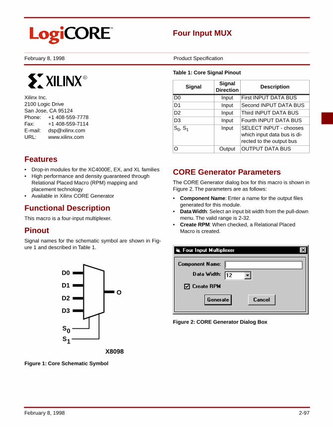
Four Input MUX
February 8, 1998 Product Specification
Xilinx Inc.2100 Logic DriveSan Jose, CA 95124Phone: +1 408-559-7778Fax: +1 408-559-7114E-mail: [email protected]: www.xilinx.com
R
Features• Drop-in modules for the XC4000E, EX, and XL families• High performance and density guaranteed through
Relational Placed Macro (RPM) mapping and placement technology
• Available in Xilinx CORE Generator
Functional DescriptionThis macro is a four-input multiplexer.
PinoutSignal names for the schematic symbol are shown in Fig-ure 1 and described in Table 1.
Figure 1: Core Schematic Symbol
Table 1: Core Signal Pinout
CORE Generator ParametersThe CORE Generator dialog box for this macro is shown inFigure 2. The parameters are as follows:
• Component Name : Enter a name for the output files generated for this module.
• Data Width : Select an input bit width from the pull-down menu. The valid range is 2-32.
• Create RPM : When checked, a Relational Placed Macro is created.
Figure 2: CORE Generator Dialog Box
O
D0
X8098
S
D1
D2
D3
0S1
Signal Signal
DirectionDescription
D0 Input First INPUT DATA BUSD1 Input Second INPUT DATA BUSD2 Input Third INPUT DATA BUSD3 Input Fourth INPUT DATA BUSS0, S1 Input SELECT INPUT - chooses
which input data bus is di-rected to the output bus
O Output OUTPUT DATA BUS
February 8, 1998 2-97

Four Input MUXFour Input MUX
Core Resource UtilizationTable 2 shows the number of CLBs required for each avail-able bit width.
Table 2: Bit Width versus CLB Count
Ordering InformationThis macro comes free with the Xilinx CORE Generator.For additional information contact your local Xilinx salesrepresentative, or e-mail requests to [email protected].
Bit Width CLB Count2 23 34 45 56 67 78 89 9
10 1011 1112 1213 1314 1415 1516 1617 1718 1819 1920 2021 2122 2223 2324 2425 2526 2627 2728 2829 2930 3031 3132 32
2-98 February 8, 1998
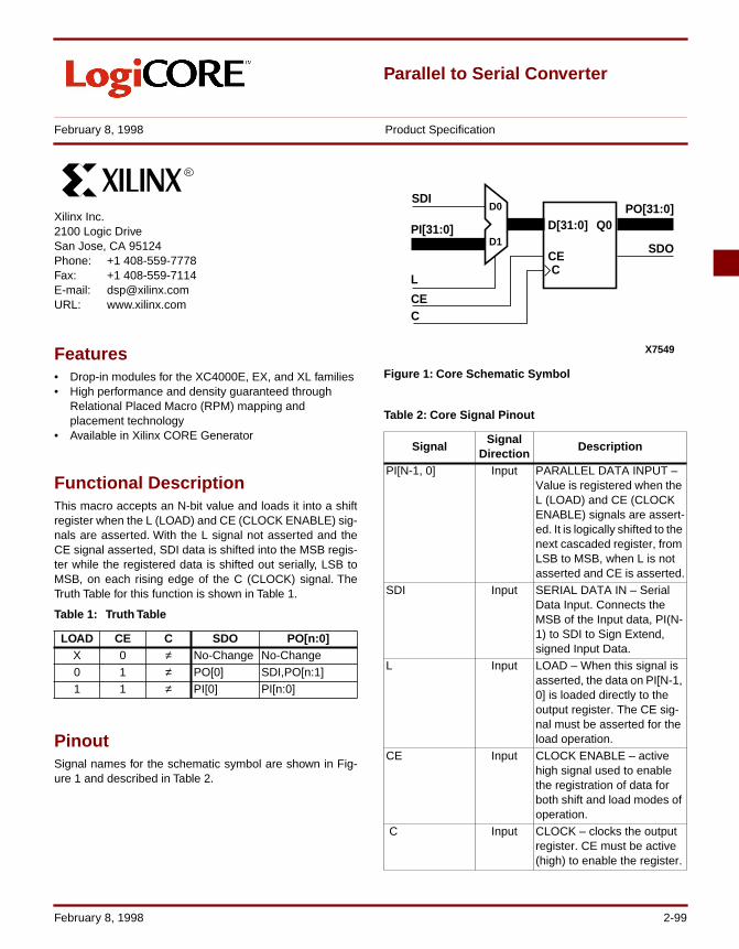
Parallel to Serial Converter
February 8, 1998 Product Specification
Xilinx Inc.2100 Logic DriveSan Jose, CA 95124Phone: +1 408-559-7778Fax: +1 408-559-7114E-mail: [email protected]: www.xilinx.com
R
Features• Drop-in modules for the XC4000E, EX, and XL families• High performance and density guaranteed through
Relational Placed Macro (RPM) mapping and placement technology
• Available in Xilinx CORE Generator
Functional DescriptionThis macro accepts an N-bit value and loads it into a shiftregister when the L (LOAD) and CE (CLOCK ENABLE) sig-nals are asserted. With the L signal not asserted and theCE signal asserted, SDI data is shifted into the MSB regis-ter while the registered data is shifted out serially, LSB toMSB, on each rising edge of the C (CLOCK) signal. TheTruth Table for this function is shown in Table 1.
Table 1: Truth Table
PinoutSignal names for the schematic symbol are shown in Fig-ure 1 and described in Table 2.
Figure 1: Core Schematic Symbol
Table 2: Core Signal Pinout
LOAD CE C SDO PO[n:0]X 0 ≠ No-Change No-Change0 1 ≠ PO[0] SDI,PO[n:1]1 1 ≠ PI[0] PI[n:0]
SignalSignal
DirectionDescription
PI[N-1, 0] Input PARALLEL DATA INPUT – Value is registered when the L (LOAD) and CE (CLOCK ENABLE) signals are assert-ed. It is logically shifted to the next cascaded register, from LSB to MSB, when L is not asserted and CE is asserted.
SDI Input SERIAL DATA IN – Serial Data Input. Connects the MSB of the Input data, PI(N-1) to SDI to Sign Extend, signed Input Data.
L Input LOAD – When this signal is asserted, the data on PI[N-1, 0] is loaded directly to the output register. The CE sig-nal must be asserted for the load operation.
CE Input CLOCK ENABLE – active high signal used to enable the registration of data for both shift and load modes of operation.
C Input CLOCK – clocks the output register. CE must be active (high) to enable the register.
SDI
PI[31:0]
CE
L
C
CEC
D[31:0] Q0PO[31:0]D0
D1
X7549
SDO
February 8, 1998 2-99
Parallel to Serial ConverterParallel to Serial Converter
CORE Generator ParametersThe CORE Generator dialog box for this macro is shown inFigure 2. The parameters are as follows:
• Component Name : Enter a name for the output files generated for this module.
• Data Width : Select an input bit width from the pull-down menu. The valid range is 2-32.
• Create RPM : When checked, a Relational Placed Macro is created.
Figure 2: CORE Generator Dialog Box
Ordering InformationThis macro comes free with the Xilinx CORE Generator.For additional information contact your local Xilinx salesrepresentative, or e-mail requests to [email protected].
Core Resource UtilizationTable 3 shows the number of CLBs required for each avail-able bit width.
Table 3: Bit Width versus CLB Count SDO Output SERIAL DATA OUTPUT –
Serial, LSB to MSB output bit of shift parallel data.
PO[N-1, 0] Output PARALLEL DATA OUTPUT – Parallel Data output bits of shifted parallel data. This output can be used for serial to parallel conversion in as-sociation with the SDI.
SignalSignal
DirectionDescription
Bit Width CLB Count2 13 24 25 36 37 48 49 5
10 511 612 613 714 715 816 817 918 919 1020 1021 1122 1123 1224 1225 1326 1327 1428 1429 1530 1531 1632 16
2-100 February 8, 1998
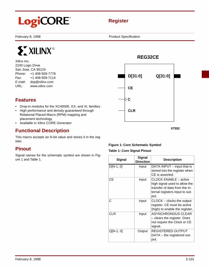
Register
February 8, 1998 Product Specification
Xilinx Inc.2100 Logic DriveSan Jose, CA 95124Phone: +1 408-559-7778Fax: +1 408-559-7114E-mail: [email protected]: www.xilinx.com
R
Features• Drop-in modules for the XC4000E, EX, and XL families• High performance and density guaranteed through
Relational Placed Macro (RPM) mapping and placement technology
• Available in Xilinx CORE Generator
Functional DescriptionThis macro accepts an N-bit value and stores it in the reg-ister.
Pinout Signal names for the schematic symbol are shown in Fig-ure 1 and Table 1.
Figure 1: Core Schematic Symbol
Table 1: Core Signal Pinout
SignalSignal
DirectionDescription
D[N-1, 0] Input DATA INPUT – input that is stored into the register when CE is asserted.
CE Input CLOCK ENABLE – active high signal used to allow the transfer of data from the in-ternal registers input to out-put.
C Input CLOCK – clocks the output register. CE must be active (high) to enable the register.
CLR Input ASYNCHRONOUS CLEAR – clears the register. Does not require the Clock or CE signal.
Q[N-1, 0] Output REGISTERED OUTPUT DATA – the registered out-put.
REG32CE
X7552
CE
C
D[31:0] Q[31:0]
CLR
February 8, 1998 2-101
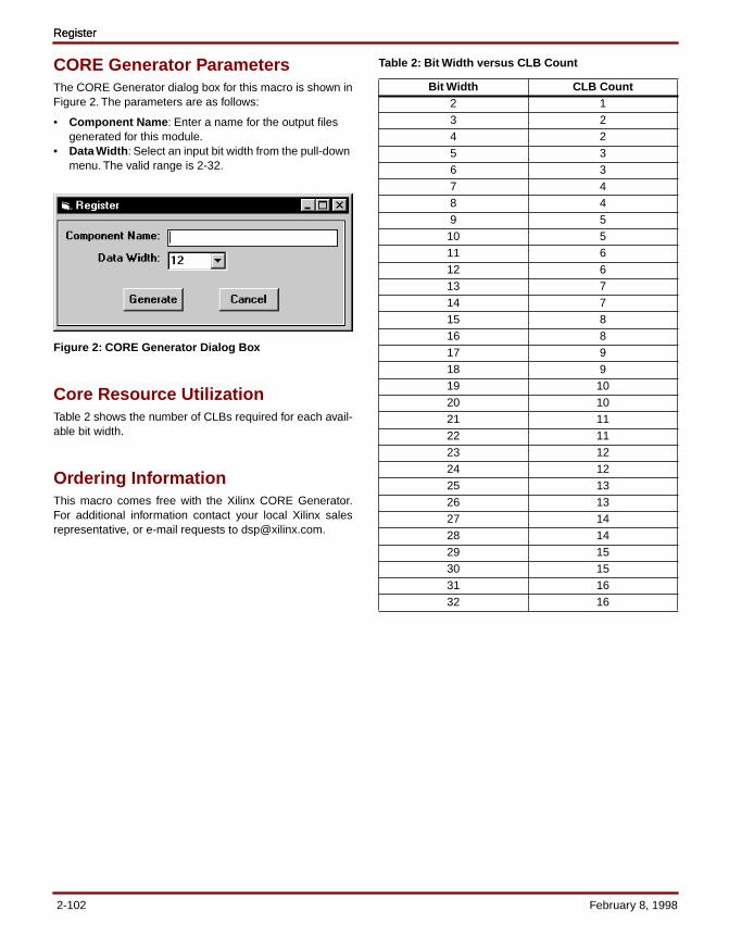
RegisterRegister
CORE Generator ParametersThe CORE Generator dialog box for this macro is shown inFigure 2. The parameters are as follows:
• Component Name : Enter a name for the output files generated for this module.
• Data Width : Select an input bit width from the pull-down menu. The valid range is 2-32.
Figure 2: CORE Generator Dialog Box
Core Resource UtilizationTable 2 shows the number of CLBs required for each avail-able bit width.
Ordering InformationThis macro comes free with the Xilinx CORE Generator.For additional information contact your local Xilinx salesrepresentative, or e-mail requests to [email protected].
Table 2: Bit Width versus CLB Count
Bit Width CLB Count2 13 24 25 36 37 48 49 5
10 511 612 613 714 715 816 817 918 919 1020 1021 1122 1123 1224 1225 1326 1327 1428 1429 1530 1531 1632 16
2-102 February 8, 1998
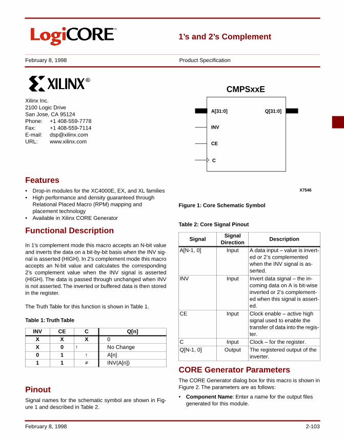
1’s and 2’s Complement
February 8, 1998 Product Specification
Xilinx Inc.2100 Logic DriveSan Jose, CA 95124Phone: +1 408-559-7778Fax: +1 408-559-7114E-mail: [email protected]: www.xilinx.com
R
Features• Drop-in modules for the XC4000E, EX, and XL families• High performance and density guaranteed through
Relational Placed Macro (RPM) mapping and placement technology
• Available in Xilinx CORE Generator
Functional Description
In 1’s complement mode this macro accepts an N-bit valueand inverts the data on a bit-by-bit basis when the INV sig-nal is asserted (HIGH). In 2’s complement mode this macroaccepts an N-bit value and calculates the corresponding2’s complement value when the INV signal is asserted(HIGH). The data is passed through unchanged when INVis not asserted. The inverted or buffered data is then storedin the register.
The Truth Table for this function is shown in Table 1.
Table 1: Truth Table
PinoutSignal names for the schematic symbol are shown in Fig-ure 1 and described in Table 2.
Figure 1: Core Schematic Symbol
Table 2: Core Signal Pinout
CORE Generator ParametersThe CORE Generator dialog box for this macro is shown inFigure 2. The parameters are as follows:
• Component Name : Enter a name for the output files generated for this module.
INV CE C Q[n]X X X 0X 0 ↑ No Change0 1 ↑ A[n]1 1 ≠ INV(A[n])
R
SignalSignal
DirectionDescription
A[N-1, 0] Input A data input – value is invert-ed or 2’s complemented when the INV signal is as-serted.
INV Input Invert data signal – the in-coming data on A is bit-wise inverted or 2’s complement-ed when this signal is assert-ed.
CE Input Clock enable – active high signal used to enable the transfer of data into the regis-ter.
C Input Clock – for the register.Q[N-1, 0] Output The registered output of the
inverter.
CMPSxxE
X7546
INV
CE
C
A[31:0] Q[31:0]
February 8, 1998 2-103
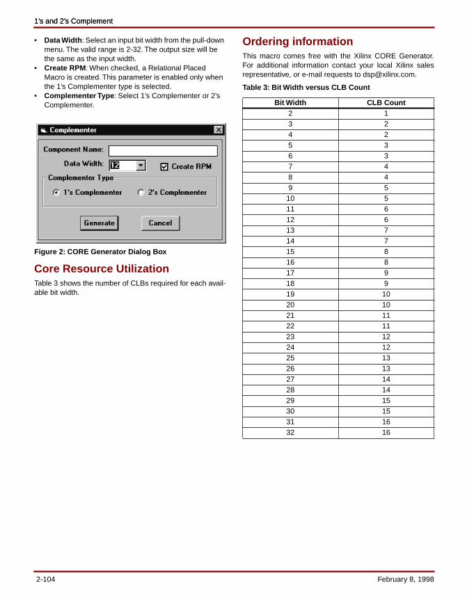
1’s and 2’s Complement1’s and 2’s Complement
• Data Width : Select an input bit width from the pull-down menu. The valid range is 2-32. The output size will be the same as the input width.
• Create RPM : When checked, a Relational Placed Macro is created. This parameter is enabled only when the 1’s Complementer type is selected.
• Complementer Type : Select 1’s Complementer or 2’s Complementer.
Figure 2: CORE Generator Dialog Box
Core Resource UtilizationTable 3 shows the number of CLBs required for each avail-able bit width.
Ordering informationThis macro comes free with the Xilinx CORE Generator.For additional information contact your local Xilinx salesrepresentative, or e-mail requests to [email protected].
Table 3: Bit Width versus CLB Count
Bit Width CLB Count2 13 24 25 36 37 48 49 5
10 511 612 613 714 715 816 817 918 919 1020 1021 1122 1123 1224 1225 1326 1327 1428 1429 1530 1531 1632 16
2-104 February 8, 1998
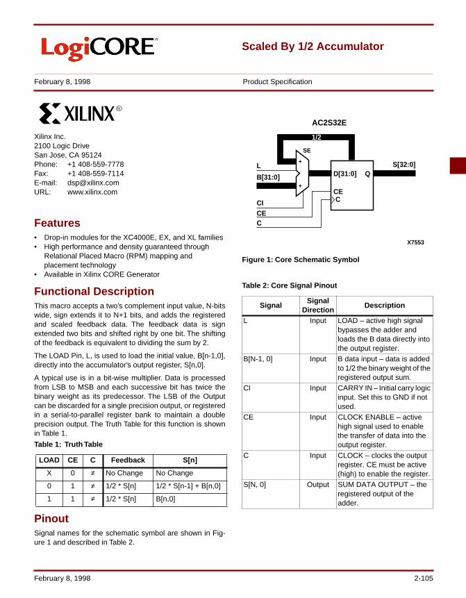
Scaled By 1/2 Accumulator
February 8, 1998 Product Specification
Xilinx Inc.2100 Logic DriveSan Jose, CA 95124Phone: +1 408-559-7778Fax: +1 408-559-7114E-mail: [email protected]: www.xilinx.com
R
Features• Drop-in modules for the XC4000E, EX, and XL families• High performance and density guaranteed through
Relational Placed Macro (RPM) mapping and placement technology
• Available in Xilinx CORE Generator
Functional DescriptionThis macro accepts a two’s complement input value, N-bitswide, sign extends it to N+1 bits, and adds the registeredand scaled feedback data. The feedback data is signextended two bits and shifted right by one bit. The shiftingof the feedback is equivalent to dividing the sum by 2.
The LOAD Pin, L, is used to load the initial value, B[n-1,0],directly into the accumulator’s output register, S[n,0].
A typical use is in a bit-wise multiplier. Data is processedfrom LSB to MSB and each successive bit has twice thebinary weight as its predecessor. The LSB of the Outputcan be discarded for a single precision output, or registeredin a serial-to-parallel register bank to maintain a doubleprecision output. The Truth Table for this function is shownin Table 1.
PinoutSignal names for the schematic symbol are shown in Fig-ure 1 and described in Table 2.
Figure 1: Core Schematic Symbol
Table 2: Core Signal Pinout
Table 1: Truth Table
LOAD CE C Feedback S[n]
X 0 ≠ No Change No Change
0 1 ≠ 1/2 * S[n] 1/2 * S[n-1] + B[n,0]
1 1 ≠ 1/2 * S[n] B[n,0]
SignalSignal
DirectionDescription
L Input LOAD – active high signal bypasses the adder and loads the B data directly into the output register.
B[N-1, 0] Input B data input – data is added to 1/2 the binary weight of the registered output sum.
Cl Input CARRY IN – Initial carry logic input. Set this to GND if not used.
CE Input CLOCK ENABLE – active high signal used to enable the transfer of data into the output register.
C Input CLOCK – clocks the output register. CE must be active (high) to enable the register.
S[N, 0] Output SUM DATA OUTPUT – the registered output of the adder.
L
B[31:0]
CECI
C
CEC
D[31:0] QS[32:0]
SE
AC2S32E
+
+
X7553
1/2
February 8, 1998 2-105
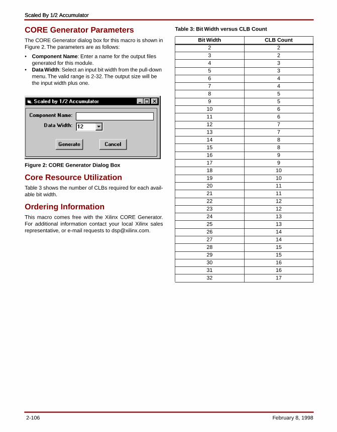
Scaled By 1/2 AccumulatorScaled By 1/2 Accumulator
CORE Generator ParametersThe CORE Generator dialog box for this macro is shown inFigure 2. The parameters are as follows:
• Component Name : Enter a name for the output files generated for this module.
• Data Width : Select an input bit width from the pull-down menu. The valid range is 2-32. The output size will be the input width plus one.
Figure 2: CORE Generator Dialog Box
Core Resource UtilizationTable 3 shows the number of CLBs required for each avail-able bit width.
Ordering InformationThis macro comes free with the Xilinx CORE Generator.For additional information contact your local Xilinx salesrepresentative, or e-mail requests to [email protected].
Table 3: Bit Width versus CLB Count
Bit Width CLB Count2 23 24 35 36 47 48 59 5
10 611 612 713 714 815 816 917 918 1019 1020 1121 1122 1223 1224 1325 1326 1427 1428 1529 1530 1631 1632 17
2-106 February 8, 1998
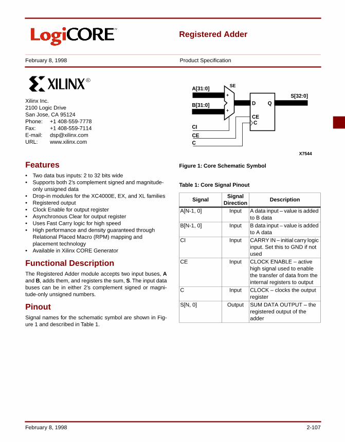
Registered Adder
February 8, 1998 Product Specification
Xilinx Inc.2100 Logic DriveSan Jose, CA 95124Phone: +1 408-559-7778Fax: +1 408-559-7114E-mail: [email protected]: www.xilinx.com
R
Features• Two data bus inputs: 2 to 32 bits wide• Supports both 2’s complement signed and magnitude-
only unsigned data• Drop-in modules for the XC4000E, EX, and XL families• Registered output• Clock Enable for output register• Asynchronous Clear for output register• Uses Fast Carry logic for high speed• High performance and density guaranteed through
Relational Placed Macro (RPM) mapping and placement technology
• Available in Xilinx CORE Generator
Functional DescriptionThe Registered Adder module accepts two input buses, Aand B, adds them, and registers the sum, S. The input databuses can be in either 2’s complement signed or magni-tude-only unsigned numbers.
PinoutSignal names for the schematic symbol are shown in Fig-ure 1 and described in Table 1.
Figure 1: Core Schematic Symbol
Table 1: Core Signal Pinout
Signal Signal
DirectionDescription
A[N-1, 0] Input A data input – value is added to B data
B[N-1, 0] Input B data input – value is added to A data
CI Input CARRY IN – initial carry logic input. Set this to GND if not used
CE Input CLOCK ENABLE – active high signal used to enable the transfer of data from the internal registers to output
C Input CLOCK – clocks the output register
S[N, 0] Output SUM DATA OUTPUT – the registered output of the adder
A[31:0]
B[31:0]
CE
CI
C
CEC
D QS[32:0]
SE
+
+
X7544
February 8, 1998 2-107
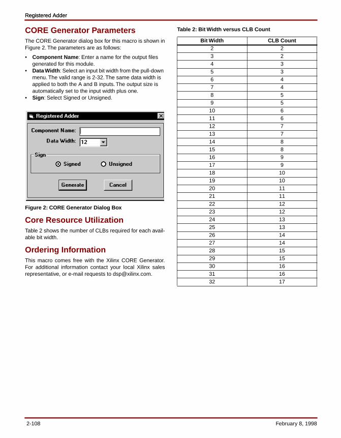
Registered AdderRegistered Adder
CORE Generator ParametersThe CORE Generator dialog box for this macro is shown inFigure 2. The parameters are as follows:
• Component Name : Enter a name for the output files generated for this module.
• Data Width : Select an input bit width from the pull-down menu. The valid range is 2-32. The same data width is applied to both the A and B inputs. The output size is automatically set to the input width plus one.
• Sign : Select Signed or Unsigned.
Figure 2: CORE Generator Dialog Box
Core Resource UtilizationTable 2 shows the number of CLBs required for each avail-able bit width.
Ordering InformationThis macro comes free with the Xilinx CORE Generator.For additional information contact your local Xilinx salesrepresentative, or e-mail requests to [email protected].
Table 2: Bit Width versus CLB Count
Bit Width CLB Count2 23 24 35 36 47 48 59 5
10 611 612 713 714 815 816 917 918 1019 1020 1121 1122 1223 1224 1325 1326 1427 1428 1529 1530 1631 1632 17
2-108 February 8, 1998
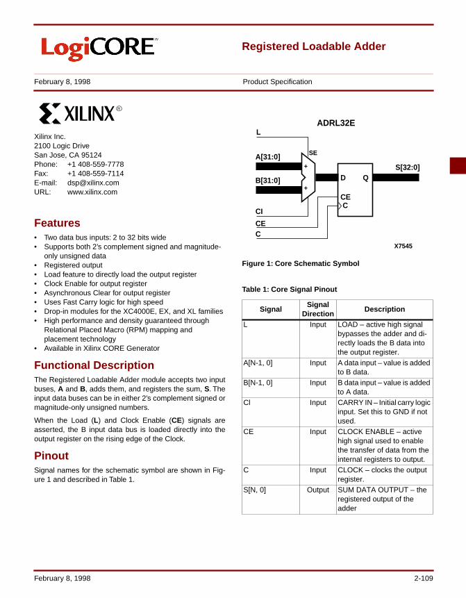
Registered Loadable Adder
February 8, 1998 Product Specification
Xilinx Inc.2100 Logic DriveSan Jose, CA 95124Phone: +1 408-559-7778Fax: +1 408-559-7114E-mail: [email protected]: www.xilinx.com
R
Features• Two data bus inputs: 2 to 32 bits wide• Supports both 2’s complement signed and magnitude-
only unsigned data• Registered output• Load feature to directly load the output register• Clock Enable for output register• Asynchronous Clear for output register• Uses Fast Carry logic for high speed• Drop-in modules for the XC4000E, EX, and XL families• High performance and density guaranteed through
Relational Placed Macro (RPM) mapping and placement technology
• Available in Xilinx CORE Generator
Functional DescriptionThe Registered Loadable Adder module accepts two inputbuses, A and B, adds them, and registers the sum, S. Theinput data buses can be in either 2’s complement signed ormagnitude-only unsigned numbers.
When the Load (L) and Clock Enable (CE) signals areasserted, the B input data bus is loaded directly into theoutput register on the rising edge of the Clock.
PinoutSignal names for the schematic symbol are shown in Fig-ure 1 and described in Table 1.
Figure 1: Core Schematic Symbol
Table 1: Core Signal Pinout
SignalSignal
DirectionDescription
L Input LOAD – active high signal bypasses the adder and di-rectly loads the B data into the output register.
A[N-1, 0] Input A data input – value is added to B data.
B[N-1, 0] Input B data input – value is added to A data.
Cl Input CARRY IN – Initial carry logic input. Set this to GND if not used.
CE Input CLOCK ENABLE – active high signal used to enable the transfer of data from the internal registers to output.
C Input CLOCK – clocks the output register.
S[N, 0] Output SUM DATA OUTPUT – the registered output of the adder
A[31:0]
B[31:0]
CE
CI
C
CEC
D QS[32:0]
SE
ADRL32E
+
+
X7545
L
February 8, 1998 2-109
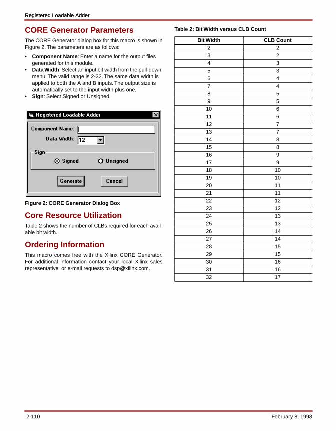
Registered Loadable AdderRegistered Loadable Adder
CORE Generator ParametersThe CORE Generator dialog box for this macro is shown inFigure 2. The parameters are as follows:
• Component Name : Enter a name for the output files generated for this module.
• Data Width : Select an input bit width from the pull-down menu. The valid range is 2-32. The same data width is applied to both the A and B inputs. The output size is automatically set to the input width plus one.
• Sign : Select Signed or Unsigned.
Figure 2: CORE Generator Dialog Box
Core Resource UtilizationTable 2 shows the number of CLBs required for each avail-able bit width.
Ordering InformationThis macro comes free with the Xilinx CORE Generator.For additional information contact your local Xilinx salesrepresentative, or e-mail requests to [email protected].
Table 2: Bit Width versus CLB Count
Bit Width CLB Count2 23 24 35 36 47 48 59 5
10 611 612 713 714 815 816 917 918 1019 1020 1121 1122 1223 1224 1325 1326 1427 1428 1529 1530 1631 1632 17
2-110 February 8, 1998
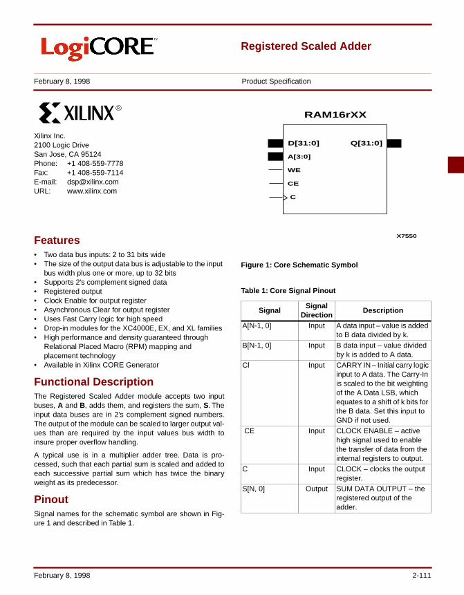
Registered Scaled Adder
February 8, 1998 Product Specification
Xilinx Inc.2100 Logic DriveSan Jose, CA 95124Phone: +1 408-559-7778Fax: +1 408-559-7114E-mail: [email protected]: www.xilinx.com
R
Features• Two data bus inputs: 2 to 31 bits wide• The size of the output data bus is adjustable to the input
bus width plus one or more, up to 32 bits• Supports 2’s complement signed data• Registered output• Clock Enable for output register• Asynchronous Clear for output register• Uses Fast Carry logic for high speed• Drop-in modules for the XC4000E, EX, and XL families• High performance and density guaranteed through
Relational Placed Macro (RPM) mapping and placement technology
• Available in Xilinx CORE Generator
Functional DescriptionThe Registered Scaled Adder module accepts two inputbuses, A and B, adds them, and registers the sum, S. Theinput data buses are in 2’s complement signed numbers.The output of the module can be scaled to larger output val-ues than are required by the input values bus width toinsure proper overflow handling.
A typical use is in a multiplier adder tree. Data is pro-cessed, such that each partial sum is scaled and added toeach successive partial sum which has twice the binaryweight as its predecessor.
PinoutSignal names for the schematic symbol are shown in Fig-ure 1 and described in Table 1.
Figure 1: Core Schematic Symbol
Table 1: Core Signal Pinout
Signal Signal
DirectionDescription
A[N-1, 0] Input A data input – value is added to B data divided by k.
B[N-1, 0] Input B data input – value divided by k is added to A data.
Cl Input CARRY IN – Initial carry logic input to A data. The Carry-In is scaled to the bit weighting of the A Data LSB, which equates to a shift of k bits for the B data. Set this input to GND if not used.
CE Input CLOCK ENABLE – active high signal used to enable the transfer of data from the internal registers to output.
C Input CLOCK – clocks the output register.
S[N, 0] Output SUM DATA OUTPUT – the registered output of the adder.
RAM16rXX
X7550
CE
D[31:0] Q[31:0]
C
A[3:0]
WE
February 8, 1998 2-111
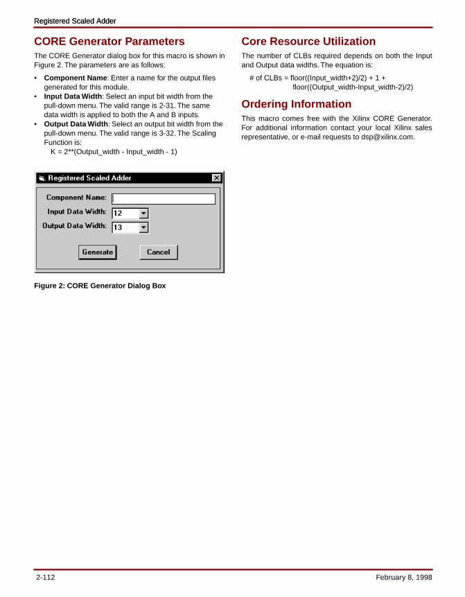
Registered Scaled AdderRegistered Scaled Adder
CORE Generator Parameters The CORE Generator dialog box for this macro is shown inFigure 2. The parameters are as follows:
• Component Name : Enter a name for the output files generated for this module.
• Input Data Width : Select an input bit width from the pull-down menu. The valid range is 2-31. The same data width is applied to both the A and B inputs.
• Output Data Width : Select an output bit width from the pull-down menu. The valid range is 3-32. The Scaling Function is:
K = 2**(Output_width - Input_width - 1)
Figure 2: CORE Generator Dialog Box
Core Resource UtilizationThe number of CLBs required depends on both the Inputand Output data widths. The equation is:
# of CLBs = floor((Input_width+2)/2) + 1 + floor((Output_width-Input_width-2)/2)
Ordering InformationThis macro comes free with the Xilinx CORE Generator.For additional information contact your local Xilinx salesrepresentative, or e-mail requests to [email protected].
2-112 February 8, 1998
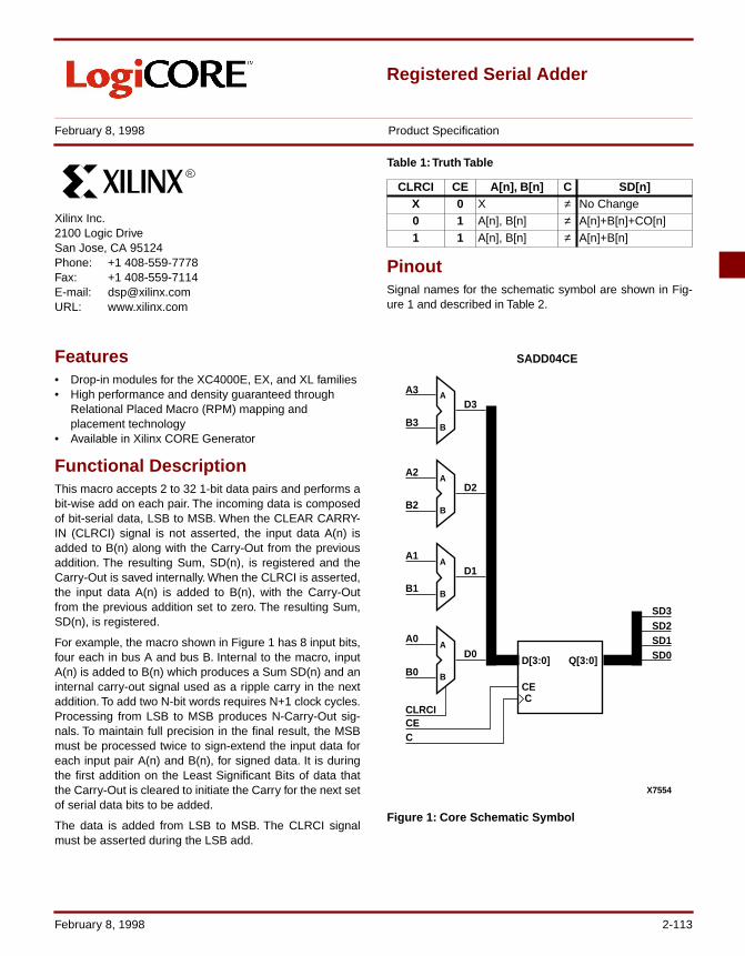
Registered Serial Adder
February 8, 1998 Product Specification
Xilinx Inc.2100 Logic DriveSan Jose, CA 95124Phone: +1 408-559-7778Fax: +1 408-559-7114E-mail: [email protected]: www.xilinx.com
R
Features• Drop-in modules for the XC4000E, EX, and XL families• High performance and density guaranteed through
Relational Placed Macro (RPM) mapping and placement technology
• Available in Xilinx CORE Generator
Functional DescriptionThis macro accepts 2 to 32 1-bit data pairs and performs abit-wise add on each pair. The incoming data is composedof bit-serial data, LSB to MSB. When the CLEAR CARRY-IN (CLRCI) signal is not asserted, the input data A(n) isadded to B(n) along with the Carry-Out from the previousaddition. The resulting Sum, SD(n), is registered and theCarry-Out is saved internally. When the CLRCI is asserted,the input data A(n) is added to B(n), with the Carry-Outfrom the previous addition set to zero. The resulting Sum,SD(n), is registered.
For example, the macro shown in Figure 1 has 8 input bits,four each in bus A and bus B. Internal to the macro, inputA(n) is added to B(n) which produces a Sum SD(n) and aninternal carry-out signal used as a ripple carry in the nextaddition. To add two N-bit words requires N+1 clock cycles.Processing from LSB to MSB produces N-Carry-Out sig-nals. To maintain full precision in the final result, the MSBmust be processed twice to sign-extend the input data foreach input pair A(n) and B(n), for signed data. It is duringthe first addition on the Least Significant Bits of data thatthe Carry-Out is cleared to initiate the Carry for the next setof serial data bits to be added.
The data is added from LSB to MSB. The CLRCI signalmust be asserted during the LSB add.
Table 1: Truth Table
PinoutSignal names for the schematic symbol are shown in Fig-ure 1 and described in Table 2.
Figure 1: Core Schematic Symbol
CLRCI CE A[n], B[n] C SD[n]X 0 X ≠ No Change0 1 A[n], B[n] ≠ A[n]+B[n]+CO[n]1 1 A[n], B[n] ≠ A[n]+B[n]
CEC
CEC
D[3:0] Q[3:0] SD0
SADD04CE
X7554
A
B
A
B
A
B
A
B
A0
B0
A1
B1
A2
B2
A3
B3
CLRCI
SD1SD2SD3
D0
D1
D2
D3
February 8, 1998 2-113
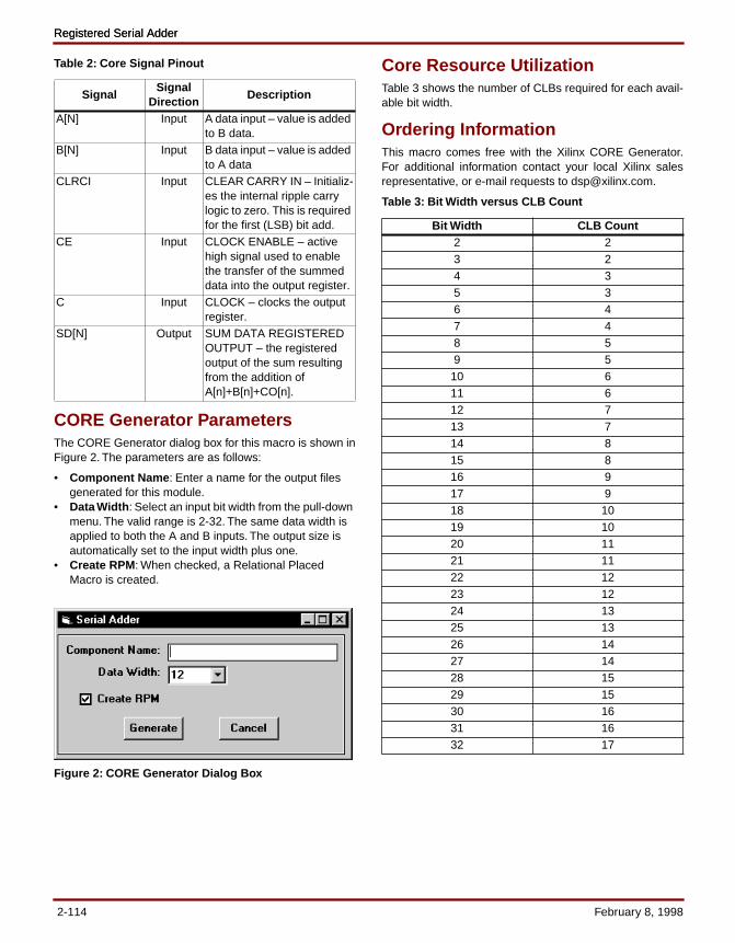
Registered Serial AdderRegistered Serial Adder
Table 2: Core Signal Pinout
CORE Generator ParametersThe CORE Generator dialog box for this macro is shown inFigure 2. The parameters are as follows:
• Component Name : Enter a name for the output files generated for this module.
• Data Width : Select an input bit width from the pull-down menu. The valid range is 2-32. The same data width is applied to both the A and B inputs. The output size is automatically set to the input width plus one.
• Create RPM : When checked, a Relational Placed Macro is created.
Figure 2: CORE Generator Dialog Box
Core Resource UtilizationTable 3 shows the number of CLBs required for each avail-able bit width.
Ordering InformationThis macro comes free with the Xilinx CORE Generator.For additional information contact your local Xilinx salesrepresentative, or e-mail requests to [email protected].
Table 3: Bit Width versus CLB Count
SignalSignal
DirectionDescription
A[N] Input A data input – value is added to B data.
B[N] Input B data input – value is added to A data
CLRCI Input CLEAR CARRY IN – Initializ-es the internal ripple carry logic to zero. This is required for the first (LSB) bit add.
CE Input CLOCK ENABLE – active high signal used to enable the transfer of the summed data into the output register.
C Input CLOCK – clocks the output register.
SD[N] Output SUM DATA REGISTERED OUTPUT – the registered output of the sum resulting from the addition of A[n]+B[n]+CO[n].
Bit Width CLB Count2 23 24 35 36 47 48 59 5
10 611 612 713 714 815 816 917 918 1019 1020 1121 1122 1223 1224 1325 1326 1427 1428 1529 1530 1631 1632 17
2-114 February 8, 1998
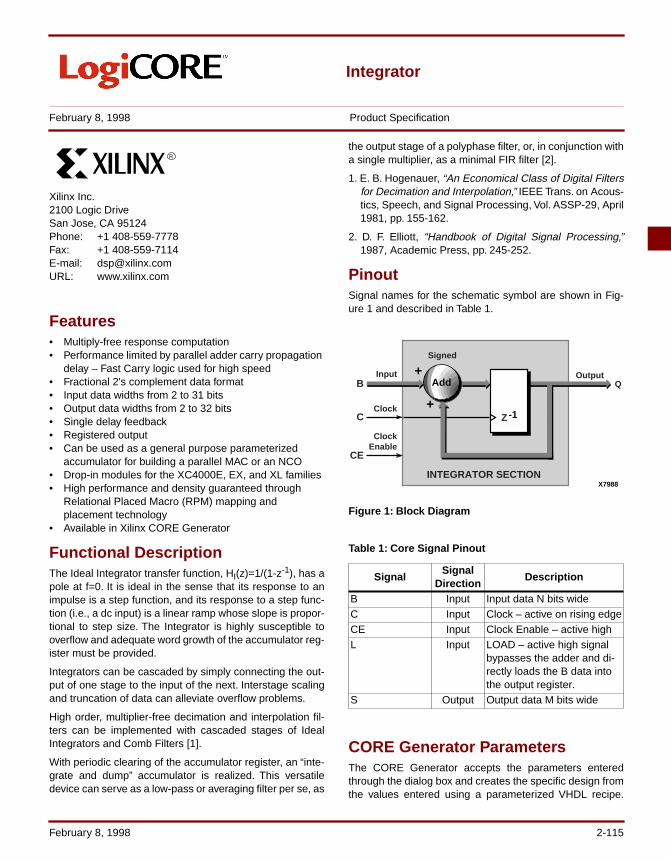
Integrator
February 8, 1998 Product Specification
Xilinx Inc.2100 Logic DriveSan Jose, CA 95124Phone: +1 408-559-7778Fax: +1 408-559-7114E-mail: [email protected]: www.xilinx.com
R
Features• Multiply-free response computation• Performance limited by parallel adder carry propagation
delay – Fast Carry logic used for high speed• Fractional 2's complement data format• Input data widths from 2 to 31 bits• Output data widths from 2 to 32 bits• Single delay feedback• Registered output• Can be used as a general purpose parameterized
accumulator for building a parallel MAC or an NCO• Drop-in modules for the XC4000E, EX, and XL families• High performance and density guaranteed through
Relational Placed Macro (RPM) mapping and placement technology
• Available in Xilinx CORE Generator
Functional DescriptionThe Ideal Integrator transfer function, HI(z)=1/(1-z-1), has apole at f=0. It is ideal in the sense that its response to animpulse is a step function, and its response to a step func-tion (i.e., a dc input) is a linear ramp whose slope is propor-tional to step size. The Integrator is highly susceptible tooverflow and adequate word growth of the accumulator reg-ister must be provided.
Integrators can be cascaded by simply connecting the out-put of one stage to the input of the next. Interstage scalingand truncation of data can alleviate overflow problems.
High order, multiplier-free decimation and interpolation fil-ters can be implemented with cascaded stages of IdealIntegrators and Comb Filters [1].
With periodic clearing of the accumulator register, an “inte-grate and dump” accumulator is realized. This versatiledevice can serve as a low-pass or averaging filter per se, as
the output stage of a polyphase filter, or, in conjunction witha single multiplier, as a minimal FIR filter [2].
1. E. B. Hogenauer, “An Economical Class of Digital Filtersfor Decimation and Interpolation,” IEEE Trans. on Acous-tics, Speech, and Signal Processing, Vol. ASSP-29, April1981, pp. 155-162.
2. D. F. Elliott, “Handbook of Digital Signal Processing,”1987, Academic Press, pp. 245-252.
PinoutSignal names for the schematic symbol are shown in Fig-ure 1 and described in Table 1.
Figure 1: Block Diagram
Table 1: Core Signal Pinout
CORE Generator ParametersThe CORE Generator accepts the parameters enteredthrough the dialog box and creates the specific design fromthe values entered using a parameterized VHDL recipe.
SignalSignal
DirectionDescription
B Input Input data N bits wideC Input Clock – active on rising edgeCE Input Clock Enable – active highL Input LOAD – active high signal
bypasses the adder and di-rectly loads the B data into the output register.
S Output Output data M bits wide
Add+
+Z-1
OutputInput
C
INTEGRATOR SECTION
B
Clock
CE
ClockEnable
Signed
Q
X7988
February 8, 1998 2-115
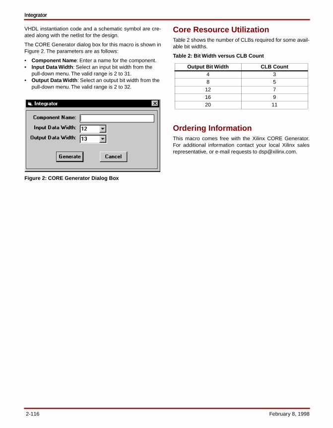
IntegratorIntegrator
VHDL instantiation code and a schematic symbol are cre-ated along with the netlist for the design.
The CORE Generator dialog box for this macro is shown inFigure 2. The parameters are as follows:
• Component Name : Enter a name for the component.• Input Data Width : Select an input bit width from the
pull-down menu. The valid range is 2 to 31.• Output Data Width : Select an output bit width from the
pull-down menu. The valid range is 2 to 32.
Figure 2: CORE Generator Dialog Box
Core Resource UtilizationTable 2 shows the number of CLBs required for some avail-able bit widths.
Table 2: Bit Width versus CLB Count
Ordering InformationThis macro comes free with the Xilinx CORE Generator.For additional information contact your local Xilinx salesrepresentative, or e-mail requests to [email protected].
Output Bit Width CLB Count4 38 5
12 716 920 11
2-116 February 8, 1998
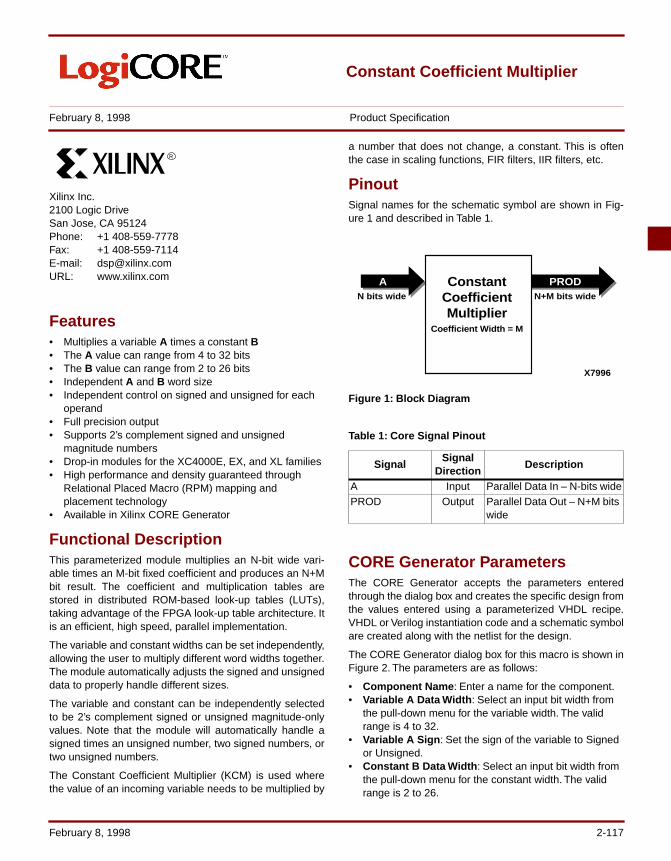
Constant Coefficient Multiplier
February 8, 1998 Product Specification
Xilinx Inc.2100 Logic DriveSan Jose, CA 95124Phone: +1 408-559-7778Fax: +1 408-559-7114E-mail: [email protected]: www.xilinx.com
R
Features• Multiplies a variable A times a constant B• The A value can range from 4 to 32 bits• The B value can range from 2 to 26 bits• Independent A and B word size• Independent control on signed and unsigned for each
operand• Full precision output• Supports 2’s complement signed and unsigned
magnitude numbers• Drop-in modules for the XC4000E, EX, and XL families• High performance and density guaranteed through
Relational Placed Macro (RPM) mapping and placement technology
• Available in Xilinx CORE Generator
Functional DescriptionThis parameterized module multiplies an N-bit wide vari-able times an M-bit fixed coefficient and produces an N+Mbit result. The coefficient and multiplication tables arestored in distributed ROM-based look-up tables (LUTs),taking advantage of the FPGA look-up table architecture. Itis an efficient, high speed, parallel implementation.
The variable and constant widths can be set independently,allowing the user to multiply different word widths together.The module automatically adjusts the signed and unsigneddata to properly handle different sizes.
The variable and constant can be independently selectedto be 2’s complement signed or unsigned magnitude-onlyvalues. Note that the module will automatically handle asigned times an unsigned number, two signed numbers, ortwo unsigned numbers.
The Constant Coefficient Multiplier (KCM) is used wherethe value of an incoming variable needs to be multiplied by
a number that does not change, a constant. This is oftenthe case in scaling functions, FIR filters, IIR filters, etc.
PinoutSignal names for the schematic symbol are shown in Fig-ure 1 and described in Table 1.
Figure 1: Block Diagram
Table 1: Core Signal Pinout
CORE Generator ParametersThe CORE Generator accepts the parameters enteredthrough the dialog box and creates the specific design fromthe values entered using a parameterized VHDL recipe.VHDL or Verilog instantiation code and a schematic symbolare created along with the netlist for the design.
The CORE Generator dialog box for this macro is shown inFigure 2. The parameters are as follows:
• Component Name : Enter a name for the component.• Variable A Data Width : Select an input bit width from
the pull-down menu for the variable width. The valid range is 4 to 32.
• Variable A Sign : Set the sign of the variable to Signed or Unsigned.
• Constant B Data Width : Select an input bit width from the pull-down menu for the constant width. The valid range is 2 to 26.
SignalSignal
DirectionDescription
A Input Parallel Data In – N-bits widePROD Output Parallel Data Out – N+M bits
wide
PRODAN bits wide N+M bits wide
ConstantCoefficientMultiplier
Coefficient Width = M
X7996
February 8, 1998 2-117
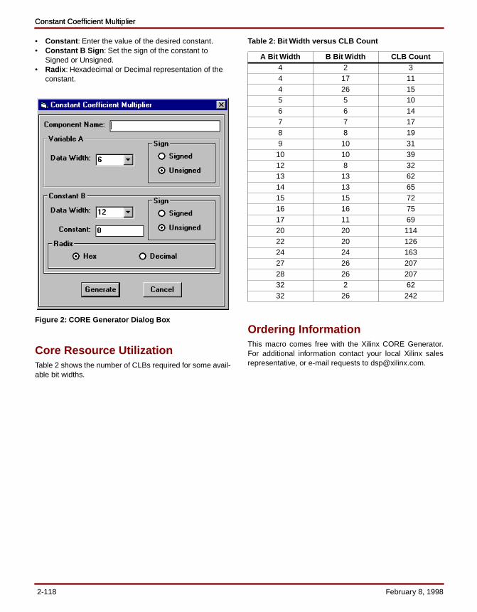
Constant Coefficient MultiplierConstant Coefficient Multiplier
• Constant : Enter the value of the desired constant.• Constant B Sign : Set the sign of the constant to
Signed or Unsigned.• Radix : Hexadecimal or Decimal representation of the
constant.
Figure 2: CORE Generator Dialog Box
Core Resource UtilizationTable 2 shows the number of CLBs required for some avail-able bit widths.
Table 2: Bit Width versus CLB Count
Ordering InformationThis macro comes free with the Xilinx CORE Generator.For additional information contact your local Xilinx salesrepresentative, or e-mail requests to [email protected].
A Bit Width B Bit Width CLB Count4 2 34 17 114 26 155 5 106 6 147 7 178 8 199 10 31
10 10 3912 8 3213 13 6214 13 6515 15 7216 16 7517 11 6920 20 11422 20 12624 24 16327 26 20728 26 20732 2 6232 26 242
2-118 February 8, 1998
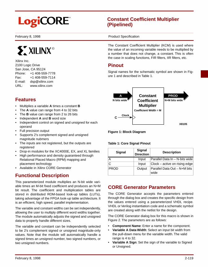
Constant Coefficient Multiplier (Pipelined)
February 8, 1998 Product Specification
Xilinx Inc.2100 Logic DriveSan Jose, CA 95124Phone: +1 408-559-7778Fax: +1 408-559-7114E-mail: [email protected]: www.xilinx.com
R
Features• Multiplies a variable A times a constant B• The A value can range from 4 to 32 bits• The B value can range from 2 to 26 bits• Independent A and B word size• Independent control on signed and unsigned for each
operand• Full precision output• Supports 2’s complement signed and unsigned
magnitude nubmers• The inputs are not registered, but the outputs are
registered• Drop-in modules for the XC4000E, EX, and XL families• High performance and density guaranteed through
Relational Placed Macro (RPM) mapping and placement technology
• Available in Xilinx CORE Generator
Functional DescriptionThis parameterized module multiplies an N-bit wide vari-able times an M-bit fixed coefficient and produces an N+Mbit result. The coefficient and multiplication tables arestored in distributed ROM-based look-up tables (LUTs),taking advantage of the FPGA look-up table architecture. Itis an efficient, high speed, parallel implementation.
The variable and constant widths can be set independently,allowing the user to multiply different word widths together.The module automatically adjusts the signed and unsigneddata to properly handle different sizes.
The variable and constant can be independently selectedto be 2’s complement signed or unsigned magnitude-onlyvalues. Note that the module will automatically handle asigned times an unsigned number, two signed numbers, ortwo unsigned numbers.
The Constant Coefficient Multiplier (KCM) is used wherethe value of an incoming variable needs to be multiplied bya number that does not change, a constant. This is oftenthe case in scaling functions, FIR filters, IIR filters, etc.
PinoutSignal names for the schematic symbol are shown in Fig-ure 1 and described in Table 1.
Figure 1: Block Diagram
Table 1: Core Signal Pinout
CORE Generator ParametersThe CORE Generator accepts the parameters enteredthrough the dialog box and creates the specific design fromthe values entered using a parameterized VHDL recipe.VHDL or Verilog instantiation code and a schematic symbolare created along with the netlist for the design.
The CORE Generator dialog box for this macro is shown inFigure 2. The parameters are as follows:
• Component Name : Enter a name for the component.• Variable A Data Width : Select an input bit width from
the pull-down menu for the variable width. The valid range is 4 to 32.
• Variable A Sign : Set the sign of the variable to Signed or Unsigned.
SignalSignal
DirectionDescription
A Input Parallel Data In – N-bits wideC Input Clock – active on rising edgePROD Output Parallel Data Out – N+M bits
wide
PRODAN bits wide N+M bits wide
CClock
ConstantCoefficientMultiplier
Coefficient Width = M
X8105
February 8, 1998 2-119
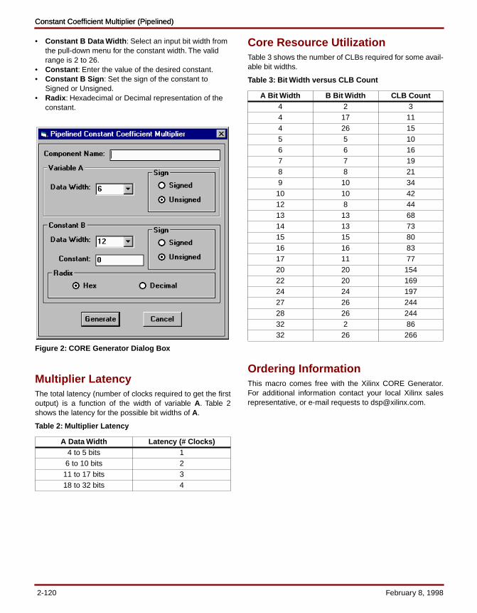
Constant Coefficient Multiplier (Pipelined)Constant Coefficient Multiplier (Pipelined)
• Constant B Data Width : Select an input bit width from the pull-down menu for the constant width. The valid range is 2 to 26.
• Constant : Enter the value of the desired constant.• Constant B Sign : Set the sign of the constant to
Signed or Unsigned.• Radix : Hexadecimal or Decimal representation of the
constant.
Figure 2: CORE Generator Dialog Box
Multiplier Latency The total latency (number of clocks required to get the firstoutput) is a function of the width of variable A. Table 2shows the latency for the possible bit widths of A.
Table 2: Multiplier Latency
Core Resource UtilizationTable 3 shows the number of CLBs required for some avail-able bit widths.
Table 3: Bit Width versus CLB Count
Ordering InformationThis macro comes free with the Xilinx CORE Generator.For additional information contact your local Xilinx salesrepresentative, or e-mail requests to [email protected].
A Data Width Latency (# Clocks)4 to 5 bits 1
6 to 10 bits 211 to 17 bits 318 to 32 bits 4
A Bit Width B Bit Width CLB Count4 2 34 17 114 26 155 5 106 6 167 7 198 8 219 10 34
10 10 4212 8 4413 13 6814 13 7315 15 8016 16 8317 11 7720 20 15422 20 16924 24 19727 26 24428 26 24432 2 8632 26 266
2-120 February 8, 1998
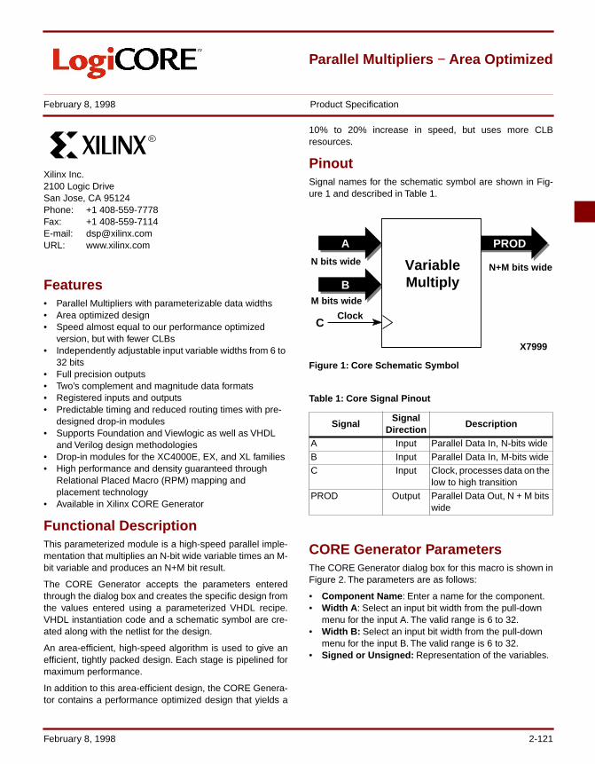
Parallel Multipliers − Area Optimized
February 8, 1998 Product Specification
Xilinx Inc.2100 Logic DriveSan Jose, CA 95124Phone: +1 408-559-7778Fax: +1 408-559-7114E-mail: [email protected]: www.xilinx.com
R
Features• Parallel Multipliers with parameterizable data widths• Area optimized design• Speed almost equal to our performance optimized
version, but with fewer CLBs• Independently adjustable input variable widths from 6 to
32 bits• Full precision outputs • Two’s complement and magnitude data formats• Registered inputs and outputs• Predictable timing and reduced routing times with pre-
designed drop-in modules• Supports Foundation and Viewlogic as well as VHDL
and Verilog design methodologies• Drop-in modules for the XC4000E, EX, and XL families• High performance and density guaranteed through
Relational Placed Macro (RPM) mapping and placement technology
• Available in Xilinx CORE Generator
Functional DescriptionThis parameterized module is a high-speed parallel imple-mentation that multiplies an N-bit wide variable times an M-bit variable and produces an N+M bit result.
The CORE Generator accepts the parameters enteredthrough the dialog box and creates the specific design fromthe values entered using a parameterized VHDL recipe.VHDL instantiation code and a schematic symbol are cre-ated along with the netlist for the design.
An area-efficient, high-speed algorithm is used to give anefficient, tightly packed design. Each stage is pipelined formaximum performance.
In addition to this area-efficient design, the CORE Genera-tor contains a performance optimized design that yields a
10% to 20% increase in speed, but uses more CLBresources.
PinoutSignal names for the schematic symbol are shown in Fig-ure 1 and described in Table 1.
Figure 1: Core Schematic Symbol
Table 1: Core Signal Pinout
CORE Generator ParametersThe CORE Generator dialog box for this macro is shown inFigure 2. The parameters are as follows:
• Component Name : Enter a name for the component.• Width A : Select an input bit width from the pull-down
menu for the input A. The valid range is 6 to 32. • Width B: Select an input bit width from the pull-down
menu for the input B. The valid range is 6 to 32. • Signed or Unsigned: Representation of the variables.
SignalSignal
DirectionDescription
A Input Parallel Data In, N-bits wideB Input Parallel Data In, M-bits wideC Input Clock, processes data on the
low to high transitionPROD Output Parallel Data Out, N + M bits
wide
PRODA
N bits wide
BM bits wide
VariableMultiply
N+M bits wide
CClock
X7999
February 8, 1998 2-121
Parallel Multipliers - Area OptimizedParallel Multipliers - Area Optimized
Figure 2: CORE Generator Dialog Box
Module LayoutFigure 3 shows the organization of CLBs in a 12x12 multi-plier. This module fits in an array of 132 CLBs organized asa matrix of 12 rows by 11 columns. The module uses 122CLBs. The white squares represent the unused CLBs,demonstrating the efficiency with which the matrix is uti-lized. The unused CLBs are available for use in other partsof the system design.
Data enters the module from the left side (A) and the bot-tom left side (B). The resulting product is available on theright side (O). If all 24 outputs are not connected to the nextstage of the design, the Xilinx implementation softwareeliminates all unused CLBs.
Figure 3: CLB Organization for Module
All of the area efficient series of modules can be built in arectangular format. For example, an 8-bit by 12-bit multi-plier will fit in a rectangular matrix of 8 rows by 11 columns.
Figure 4 shows a 12x12 multiplier in place in an XC4005Echip. The 4005E contains 196 CLBs, of which 122 are usedby the 12x12 multiplier and 74 are available for other func-tions.
Figure 4: Xilinx Floorplanner View of XC4005E with a12x12 multiplier
The module contains both relative placement informationand timing constraints, allowing the Xilinx place and routesoftware to consistently produce the same timing specifica-tions. CLB relative placement information (R-LOCs)speeds up the routing place and route time by a factor of10, thus permitting rapid design changes.
Multiplier Latency Data is buffered on the input and output of the multipliercores. The total latency (number of clocks required to getthe first output) is a function of the width of the B variableonly.
Table 2: Multiplier Latency
A11
A10
A 9
A8
A7
A6
A4
A3
A2
A5
A
A
1
O21
O19
O17
O15
O13
O11
O7
O5
O3
O9
O1
O22
O20
O18
O16
O14
O12
O8
O6
O4
O10
O2
O00
O23
B11 B7 B5 B3B9 B1B8 B6 B4B10 B2 B0
M12x12a12 rows by 11 columns
122 out of 132 CLBs used
X7990
B Data Width Latency (# Clocks)6 to 8 bits 4
9 to 16 bits 517 to 31 bits 6
2-122 February 8, 1998
Core Resource UtilizationTables 3 to 8 show the number of CLBs required for someof the available bit widths. The maximum speed is forXC4000E-1 devices.
All the variable multipliers are built to fit in a rectangular orsquare matrix of N rows by M (or M-1) columns.
Table 3: Bit Width versus CLB Count for A = 8 bits
Table 4: Bit Width versus CLB Count for A = 10 bits
Table 5: Bit Width versus CLB Count for A = 12 bits
Table 6: Bit Width versus CLB Count for A = 16 bits
Table 7: Bit Width versus CLB Count for A = 20 and 24bits
Table 8: Bit Width versus CLB Count for Other Widthsof A
A Bit Width
B Bit Width
CLB Count
4000E-1 MHz
4000E-3 MHz
8 6 44 86 548 8 54 83 538 10 86 86 538 12 96 78 468 14 111 77 458 16 124 74 448 20 180 71 438 24 211 68 418 32 282 60 35
A Bit Width
B Bit Width
CLB Count
4000E-1 MHz
4000E-3 MHz
10 6 53 81 5110 8 65 77 4910 10 100 78 4710 12 113 77 4710 14 133 70 4210 16 146 72 4410 20 209 65 3910 24 238 62 3810 32 330 57 34
A Bit Width
B Bit Width
CLB Count
4000E-1 MHz
4000E-3 MHz
12 6 61 75 4712 8 75 72 4612 10 116 70 4212 12 130 67 4112 14 153 65 4012 16 167 65 3912 20 238 63 3812 24 274 59 3612 32 371 51 31
A Bit Width
B Bit Width
CLB Count
4000E-1 MHz
4000E-3 MHz
16 6 79 64 4116 8 98 63 3916 10 148 61 3716 12 165 59 3616 14 192 56 3516 16 213 58 3516 20 299 56 3416 24 349 51 3316 32 473 49 31
A Bit Width
B Bit Width
CLB Count
4000E-1 MHz
4000E-3 MHz
20 6 98 56 3620 8 120 55 3520 12 202 55 3420 16 259 50 3120 20 358 50 3024 6 116 50 3224 8 142 50 3224 12 238 46 2824 16 305 45 2824 20 425 45 28
A Bit Width
B Bit Width
CLB Count
4000E-1 MHz
4000E-3 MHz
6 6 37 96 609 9 94 81 49
11 11 121 74 4513 13 161 61 3814 14 173 62 3715 15 203 58 3617 17 293 55 3318 18 308 53 3219 19 343 52 3232 6 151 41 2732 8 187 41 2732 12 309 41 26
February 8, 1998 2-123

Parallel Multipliers - Area OptimizedParallel Multipliers - Area Optimized
Multiplier Trade-offsTwo different implementations of parallel multipliers tradearea for speed. The area efficient designs consume aboutone-fourth less CLB resources than the high speed designsin the 4000E family.
The additional routing resources in the 4000EX and4000XL families will increase the performance for the areaefficient designs. In addition, both structures will benefitfrom the overall performance increase derived from the4000XL .35 micron process technology.
Figure 5: Trade-offs of Area Versus Speed Optimizationfor Multipliers
Ordering InformationThis macro comes free with the Xilinx CORE Generator.For additional information contact your local Xilinx salesrepresentative, or e-mail requests to [email protected].
Multipliers - MHz vs. CLBs100
40
60
50
70
90
80
10
30
20
020050 1501000 250
8x8
12x12
16x16
MH
z40
00E
-1
High Speed
Area Efficient
8x8
10x10
12x12
x7991# CLBs
2-124 February 8, 1998
Parallel Multipliers − Performance Optimized
February 8, 1998 Product Specification
Xilinx Inc.2100 Logic DriveSan Jose, CA 95124Phone: +1 408-559-7778Fax: +1 408-559-7114E-mail: [email protected]: www.xilinx.com
R
Features• High performance compact implementation• Drop-in modules for the XC4000E, EX, and XL families• Two variable operands, 2’s complement arithmetic• Signed data, full precision outputs• Registered inputs and outputs• Pre-designed modules with relative placement gives
predictable timing• Fast place and route times• Supported in Viewlogic and Foundation schematic entry
and simulation tools• VHDL and Verilog instantiation code supplied for HDL
designs• High performance and density guaranteed through
Relational Placed Macro (RPM) mapping and placement technology
• Available in Xilinx CORE Generator
General DescriptionXilinx LogiCORE™ high-speed parallel multipliers are pre-defined drop-in modules ideal for fast, real-time DSP appli-cations or any application where multiplication speed, areaefficiency, and design time are important. The multipliersuse highly efficient algorithms, tuned and optimally imple-
mented in the Xilinx XC4000E, EX, and XL series ofFPGAs.
Two parallel operands can be input to the multiplier coreevery clock cycle. A new double precision output will beavailable every clock cycle after an initial latency period.For example, a 12 by 12 multiplier can produce a resultevery 11 nsec. in a 4000E-1.
Two pre-defined modules are available: an 8x8 multiplierand a 12x12 multiplier. Table 1 gives the implementationstatistics for these modules.
PinoutSignal names for the schematic symbol are shown in Fig-ure 1 and described in Table 2.
Figure 1: Core Schematic Symbol
Table 2: Core Signal Pinout
SignalSignal
DirectionDescription
A Input Parallel Data In, N-bits wideB Input Parallel Data In, N-bits wideclk Input Clock, processes data on the
low to high transitionP Output Parallel Data Out, 2N-bits
wide
clk
N
A
B
N
Multiply(AxB=P)
2NP
X7992
Note:1. Based on XC4000E-1 advanced speed files.
Table 1: Parallel Multiplier Implementation Statistics
Design Name
Input DataOutput Data
Pin to Pin Performance 1
XC4000E-1Latency
CLBs Used
CLB Array SizeSmallest Device
M8x8 8 x 8 Signed 16 bit 97 MHz 4 clks 70 10 rows x 8 cols 4003E
M12x12 12 x 12 Signed 24 bit 89 MHz 5 clks 156 14 rows x 13 cols 4005E
February 8, 1998 2-125

Parallel Multipliers - Performance OptimizedParallel Multipliers - Performance Optimized
Multiplier Trade-offsTwo different implementations of parallel multipliers tradearea for speed. The area efficient designs consume aboutone-fourth less CLB resources than the high speed designsin the 4000E family.
The additional routing resources in the 4000EX and4000XL families will increase the performance for the areaefficient designs. In addition, both structures will benefitfrom the overall performance increase derived from the4000XL .35 micron process technology.
Figure 2: Trade-offs of Area Versus Speed Optimizationfor Multipliers
Ordering InformationThis macro comes free with the Xilinx CORE Generator.For additional information contact your local Xilinx salesrepresentative, or e-mail requests to [email protected].
Multipliers - MHz vs. CLBs100
40
60
50
70
90
80
10
30
20
020050 1501000 250
8x8
12x12
16x16
MH
z40
00E
-1
High Speed
Area Efficient
8x8
10x10
12x12
x7991# CLBs
2-126 February 8, 1998
Square Root
February 8, 1998 Product Specification
Xilinx Inc.2100 Logic DriveSan Jose, CA 95124Phone: +1 408-559-7778Fax: +1 408-559-7114E-mail: [email protected]: www.xilinx.com
R
Features• Input data widths from 4 to 64 bits• Output data widths from 4 to 64 bits• Registered output• User can determine the accuracy of the result by
selecting the desired output width• Drop-in modules for the XC4000E, EX, and XL families• High performance and density guaranteed through
Relational Placed Macro (RPM) mapping and placement technology
• Available in Xilinx CORE Generator
Functional DescriptionThe Square Root function derives the square root of aninput value.
PinoutSignal names for the schematic symbol are shown in Fig-ure 1 and described in Table 1.
Figure 1: Block Diagram
Table 1: Core Signal Pinout
CORE Generator ParametersThe CORE Generator accepts the parameters enteredthrough the dialog box and creates the specific design fromthe values entered using a parameterized VHDL recipe.VHDL instantiation code and a schematic symbol are cre-ated along with the netlist for the design.
The default output width equals one-half the input width. Ifhigher accuracy is desired, choose a higher output width,up to the value of the input width. The decimal point in theresult is always at the input_width/2 bit position.
The CORE Generator dialog box for this macro is shown inFigure 2. The parameters are as follows:
• Component Name : Enter a name for the component.• Input Data Width : Select an input bit width from the
pull-down menu. The valid range is 4 to 64.• Output Data Width : Select an output bit width from the
pull-down menu. The valid range varies with the size of input data width.
Figure 2: CORE Generator Dialog Box
LatencyThe latency equals one-half the output width.
DOUTDIN
CE
SquareRoot
M bits wideN bits wide
C
ClockEnable
Clock
X8139
SignalSignal
DirectionDescription
DIN Input Input data N bits wideC Input Clock – active on rising edgeCE Input Clock Enable – active highDOUT Output Output data M bits wide
February 8, 1998 2-127
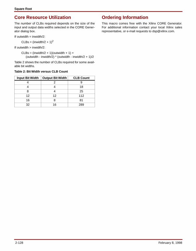
Square RootSquare Root
Core Resource UtilizationThe number of CLBs required depends on the size of theinput and output data widths selected in the CORE Gener-ator dialog box.
If outwidth = inwidth/2:
CLBs = (inwidth/2 + 1)2
If outwidth > inwidth/2:
CLBs = (inwidth/2 + 1)(outwidth + 1) + (outwidth - inwidth/2) * (outwidth - inwidth/2 + 1)/2
Table 2 shows the number of CLBs required for some avail-able bit widths.
Table 2: Bit Width versus CLB Count
Ordering InformationThis macro comes free with the Xilinx CORE Generator.For additional information contact your local Xilinx salesrepresentative, or e-mail requests to [email protected].
Input Bit Width Output Bit Width CLB Count4 2 94 4 188 4 25
12 12 11216 8 8132 16 289
2-128 February 8, 1998
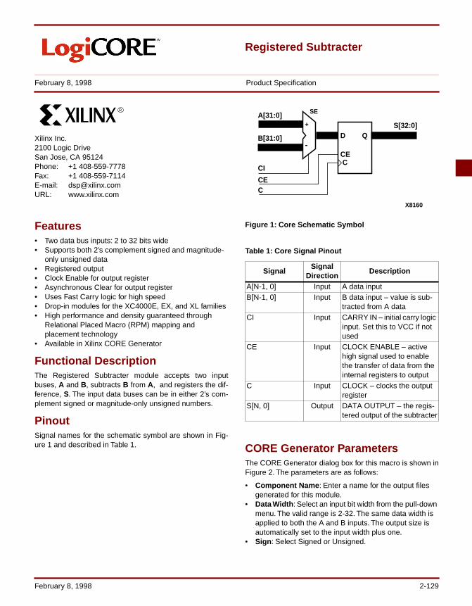
Registered Subtracter
February 8, 1998 Product Specification
Xilinx Inc.2100 Logic DriveSan Jose, CA 95124Phone: +1 408-559-7778Fax: +1 408-559-7114E-mail: [email protected]: www.xilinx.com
R
Features• Two data bus inputs: 2 to 32 bits wide• Supports both 2’s complement signed and magnitude-
only unsigned data• Registered output• Clock Enable for output register• Asynchronous Clear for output register• Uses Fast Carry logic for high speed• Drop-in modules for the XC4000E, EX, and XL families• High performance and density guaranteed through
Relational Placed Macro (RPM) mapping and placement technology
• Available in Xilinx CORE Generator
Functional DescriptionThe Registered Subtracter module accepts two inputbuses, A and B, subtracts B from A, and registers the dif-ference, S. The input data buses can be in either 2’s com-plement signed or magnitude-only unsigned numbers.
PinoutSignal names for the schematic symbol are shown in Fig-ure 1 and described in Table 1.
Figure 1: Core Schematic Symbol
Table 1: Core Signal Pinout
CORE Generator ParametersThe CORE Generator dialog box for this macro is shown inFigure 2. The parameters are as follows:
• Component Name : Enter a name for the output files generated for this module.
• Data Width : Select an input bit width from the pull-down menu. The valid range is 2-32. The same data width is applied to both the A and B inputs. The output size is automatically set to the input width plus one.
• Sign : Select Signed or Unsigned.
Signal Signal
DirectionDescription
A[N-1, 0] Input A data inputB[N-1, 0] Input B data input – value is sub-
tracted from A dataCI Input CARRY IN – initial carry logic
input. Set this to VCC if not used
CE Input CLOCK ENABLE – active high signal used to enable the transfer of data from the internal registers to output
C Input CLOCK – clocks the output register
S[N, 0] Output DATA OUTPUT – the regis-tered output of the subtracter
A[31:0]
B[31:0]
CE
CI
C
CEC
D QS[32:0]
SE
+
-
X8160
February 8, 1998 2-129
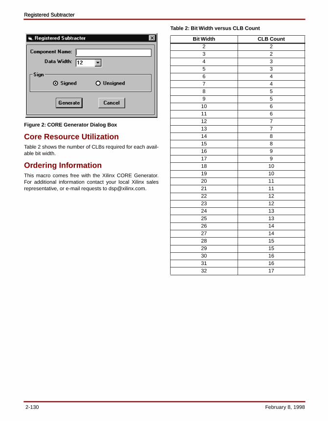
Registered SubtracterRegistered Subtracter
Figure 2: CORE Generator Dialog Box
Core Resource UtilizationTable 2 shows the number of CLBs required for each avail-able bit width.
Ordering InformationThis macro comes free with the Xilinx CORE Generator.For additional information contact your local Xilinx salesrepresentative, or e-mail requests to [email protected].
Table 2: Bit Width versus CLB Count
Bit Width CLB Count2 23 24 35 36 47 48 59 5
10 611 612 713 714 815 816 917 918 1019 1020 1121 1122 1223 1224 1325 1326 1427 1428 1529 1530 1631 1632 17
2-130 February 8, 1998
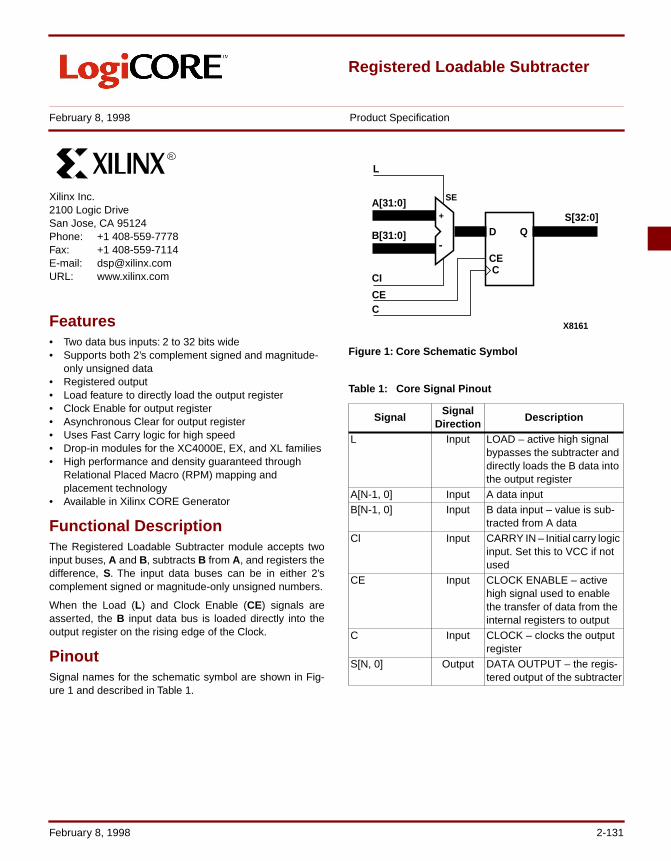
Registered Loadable Subtracter
February 8, 1998 Product Specification
Xilinx Inc.2100 Logic DriveSan Jose, CA 95124Phone: +1 408-559-7778Fax: +1 408-559-7114E-mail: [email protected]: www.xilinx.com
R
Features• Two data bus inputs: 2 to 32 bits wide• Supports both 2’s complement signed and magnitude-
only unsigned data• Registered output• Load feature to directly load the output register• Clock Enable for output register• Asynchronous Clear for output register• Uses Fast Carry logic for high speed• Drop-in modules for the XC4000E, EX, and XL families• High performance and density guaranteed through
Relational Placed Macro (RPM) mapping and placement technology
• Available in Xilinx CORE Generator
Functional DescriptionThe Registered Loadable Subtracter module accepts twoinput buses, A and B, subtracts B from A, and registers thedifference, S. The input data buses can be in either 2’scomplement signed or magnitude-only unsigned numbers.
When the Load (L) and Clock Enable (CE) signals areasserted, the B input data bus is loaded directly into theoutput register on the rising edge of the Clock.
PinoutSignal names for the schematic symbol are shown in Fig-ure 1 and described in Table 1.
Figure 1: Core Schematic Symbol
Table 1: Core Signal Pinout
SignalSignal
DirectionDescription
L Input LOAD – active high signal bypasses the subtracter and directly loads the B data into the output register
A[N-1, 0] Input A data inputB[N-1, 0] Input B data input – value is sub-
tracted from A data Cl Input CARRY IN – Initial carry logic
input. Set this to VCC if not used
CE Input CLOCK ENABLE – active high signal used to enable the transfer of data from the internal registers to output
C Input CLOCK – clocks the output register
S[N, 0] Output DATA OUTPUT – the regis-tered output of the subtracter
A[31:0]
B[31:0]
CE
CI
C
CEC
D QS[32:0]
SE
+
-
X8161
L
February 8, 1998 2-131

Registered Loadable SubtracterRegistered Loadable Subtracter
CORE Generator ParametersThe CORE Generator dialog box for this macro is shown inFigure 2. The parameters are as follows:
• Component Name : Enter a name for the output files generated for this module.
• Data Width : Select an input bit width from the pull-down menu. The valid range is 2-32. The same data width is applied to both the A and B inputs. The output size is automatically set to the input width plus one.
• Sign : Select Signed or Unsigned.
Figure 2: CORE Generator Dialog Box
Core Resource UtilizationTable 2 shows the number of CLBs required for each avail-able bit width.
Ordering InformationThis macro comes free with the Xilinx CORE Generator.For additional information contact your local Xilinx salesrepresentative, or e-mail requests to [email protected].
Table 2: Bit Width versus CLB Count
Bit Width CLB Count2 23 24 35 36 47 48 59 5
10 611 612 713 714 815 816 917 918 1019 1020 1121 1122 1223 1224 1325 1326 1427 1428 1529 1530 1631 1632 17
2-132 February 8, 1998
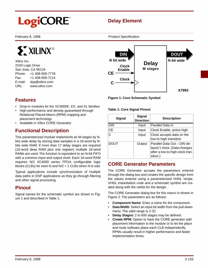
Delay Element
February 8, 1998 Product Specification
Xilinx Inc.2100 Logic DriveSan Jose, CA 95124Phone: +1 408-559-7778Fax: +1 408-559-7114E-mail: [email protected]: www.xilinx.com
R
Features• Drop-in modules for the XC4000E, EX, and XL families• High performance and density guaranteed through
Relational Placed Macro (RPM) mapping and placement technology
• Available in Xilinx CORE Generator
Functional DescriptionThis parameterized module implements an M-stages by N-bits wide delay by storing data samples in a 16-word by N-bits wide RAM. If more than 17 delay stages are required(16-word deep RAM plus one register) multiple 16-wordRAMs are used. The function is equivalent to an N-bit FIFOwith a common input and output clock. Each 16-word RAMrequires N/2 XC4000 series FPGA configurable logicblocks (CLBs) for even N and N/2 + 1 CLBs when N is odd.
Typical applications include synchronization of multipledata paths in DSP applications as they go through filteringand other signal processing.
PinoutSignal names for the schematic symbol are shown in Fig-ure 1 and described in Table 1.
Figure 1: Core Schematic Symbol
Table 1: Core Signal Pinout
CORE Generator ParametersThe CORE Generator accepts the parameters enteredthrough the dialog box and creates the specific design fromthe values entered using a parameterized VHDL recipe.VHDL instantiation code and a schematic symbol are cre-ated along with the netlist for the design.
The CORE Generator dialog box for this macro is shown inFigure 2. The parameters are as follows:
• Component Name : Enter a name for the component.• Data Width : Select an input bit width from the pull-down
menu. The valid range is 2-32. • Delay Stages: 2 to 600 stages may be defined. • Create RPM: Option to have the CORE generator add
placement information to the module or to let the place and route software place each CLB independently. RPMs usually result in higher performance and faster implementation times.
SignalSignal
DirectionDescription
DIN Input Parallel Data InCE Input Clock Enable, active highC Input Clock accepts data on the
low-to-high transitionDOUT Output Parallel Data Out – DIN de-
layed 1 clock. (Data changes after a low-to-high clock tran-sition.)
DOUTDIN
CE
DelayM stages
N bit wideN bit wide
C
ClockEnable
Clock
X7993
February 8, 1998 2-133
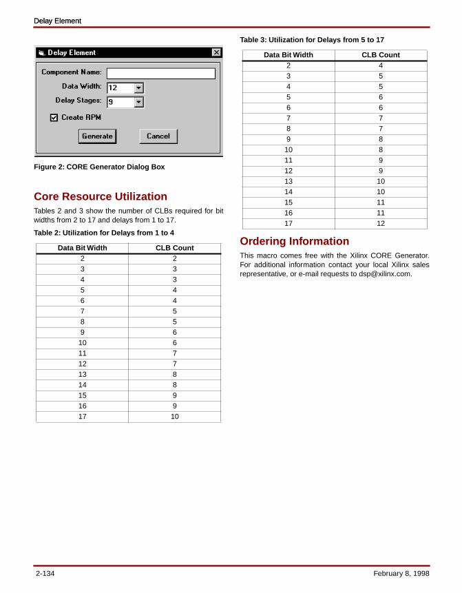
Delay ElementDelay Element
Figure 2: CORE Generator Dialog Box
Core Resource UtilizationTables 2 and 3 show the number of CLBs required for bitwidths from 2 to 17 and delays from 1 to 17.
Table 2: Utilization for Delays from 1 to 4
Table 3: Utilization for Delays from 5 to 17
Ordering InformationThis macro comes free with the Xilinx CORE Generator.For additional information contact your local Xilinx salesrepresentative, or e-mail requests to [email protected].
Data Bit Width CLB Count2 23 34 35 46 47 58 59 6
10 611 712 713 814 815 916 917 10
Data Bit Width CLB Count2 43 54 55 66 67 78 79 8
10 811 912 913 1014 1015 1116 1117 12
2-134 February 8, 1998
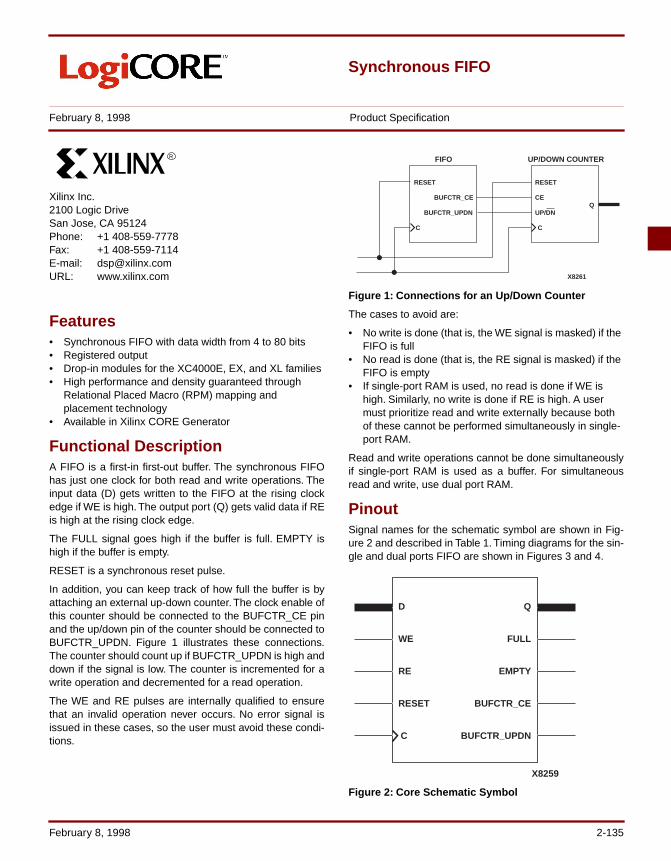
Synchronous FIFO
February 8, 1998 Product Specification
Xilinx Inc.2100 Logic DriveSan Jose, CA 95124Phone: +1 408-559-7778Fax: +1 408-559-7114E-mail: [email protected]: www.xilinx.com
R
Features• Synchronous FIFO with data width from 4 to 80 bits• Registered output• Drop-in modules for the XC4000E, EX, and XL families• High performance and density guaranteed through
Relational Placed Macro (RPM) mapping and placement technology
• Available in Xilinx CORE Generator
Functional DescriptionA FIFO is a first-in first-out buffer. The synchronous FIFOhas just one clock for both read and write operations. Theinput data (D) gets written to the FIFO at the rising clockedge if WE is high. The output port (Q) gets valid data if REis high at the rising clock edge.
The FULL signal goes high if the buffer is full. EMPTY ishigh if the buffer is empty.
RESET is a synchronous reset pulse.
In addition, you can keep track of how full the buffer is byattaching an external up-down counter. The clock enable ofthis counter should be connected to the BUFCTR_CE pinand the up/down pin of the counter should be connected toBUFCTR_UPDN. Figure 1 illustrates these connections.The counter should count up if BUFCTR_UPDN is high anddown if the signal is low. The counter is incremented for awrite operation and decremented for a read operation.
The WE and RE pulses are internally qualified to ensurethat an invalid operation never occurs. No error signal isissued in these cases, so the user must avoid these condi-tions.
Figure 1: Connections for an Up/Down Counter
The cases to avoid are:
• No write is done (that is, the WE signal is masked) if the FIFO is full
• No read is done (that is, the RE signal is masked) if the FIFO is empty
• If single-port RAM is used, no read is done if WE is high. Similarly, no write is done if RE is high. A user must prioritize read and write externally because both of these cannot be performed simultaneously in single-port RAM.
Read and write operations cannot be done simultaneouslyif single-port RAM is used as a buffer. For simultaneousread and write, use dual port RAM.
PinoutSignal names for the schematic symbol are shown in Fig-ure 2 and described in Table 1. Timing diagrams for the sin-gle and dual ports FIFO are shown in Figures 3 and 4.
Figure 2: Core Schematic Symbol
FIFO UP/DOWN COUNTER
RESET
CE
UP/DN
C
BUFCTR_CE
BUFCTR_UPDN
RESET
C
Q
X8261
D
WE
RE
RESET
C
Q
FULL
EMPTY
BUFCTR_CE
BUFCTR_UPDN
X8259
February 8, 1998 2-135

Synchronous FIFOSynchronous FIFO
C
DIN
X8263
WE
RE
DOUT
FULL
EMPTY
X DO DI X
X X X X DO DI X
Figure 3: Timing Diagram for Single and Dual Ports
C
DIN
X8262
WE
RE
DOUT
FULL
EMPTY
X DO DI X X X X
X X DO DI X X X
Figure 4: Timing Diagram for Dual Ports
2-136 February 8, 1998
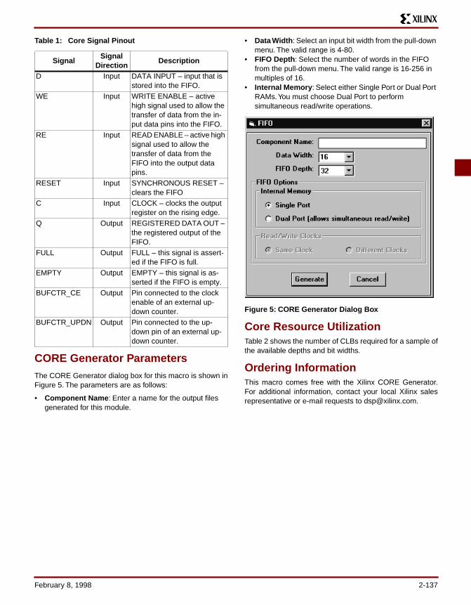
Table 1: Core Signal Pinout
CORE Generator ParametersThe CORE Generator dialog box for this macro is shown inFigure 5. The parameters are as follows:
• Component Name : Enter a name for the output files generated for this module.
• Data Width : Select an input bit width from the pull-down menu. The valid range is 4-80.
• FIFO Depth : Select the number of words in the FIFO from the pull-down menu. The valid range is 16-256 in multiples of 16.
• Internal Memory : Select either Single Port or Dual Port RAMs. You must choose Dual Port to perform simultaneous read/write operations.
Figure 5: CORE Generator Dialog Box
Core Resource UtilizationTable 2 shows the number of CLBs required for a sample ofthe available depths and bit widths.
Ordering InformationThis macro comes free with the Xilinx CORE Generator.For additional information, contact your local Xilinx salesrepresentative or e-mail requests to [email protected].
Signal Signal
DirectionDescription
D Input DATA INPUT – input that is stored into the FIFO.
WE Input WRITE ENABLE – active high signal used to allow the transfer of data from the in-put data pins into the FIFO.
RE Input READ ENABLE – active high signal used to allow the transfer of data from the FIFO into the output data pins.
RESET Input SYNCHRONOUS RESET – clears the FIFO
C Input CLOCK – clocks the output register on the rising edge.
Q Output REGISTERED DATA OUT – the registered output of the FIFO.
FULL Output FULL – this signal is assert-ed if the FIFO is full.
EMPTY Output EMPTY – this signal is as-serted if the FIFO is empty.
BUFCTR_CE Output Pin connected to the clock enable of an external up-down counter.
BUFCTR_UPDN Output Pin connected to the up-down pin of an external up-down counter.
February 8, 1998 2-137
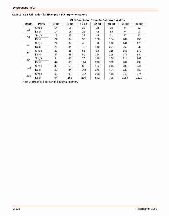
Synchronous FIFOSynchronous FIFO
Table 2: CLB Utilization for Example FIFO Implementations
Depth Ports 1
CLB Counts for Example Data Word Widths4-bit 8-bit 16-bit 32-bit 48-bit 64-bit 80-bit
16Single 14 16 20 28 36 44 52Dual 14 18 26 42 58 74 90
32Single 17 21 29 45 61 77 93Dual 22 34 58 106 154 202 250
48Single 24 32 48 80 112 144 176Dual 28 44 76 140 204 268 332
64Single 27 35 51 83 115 147 179Dual 32 48 80 144 208 272 336
96Single 34 46 70 118 166 214 262Dual 42 66 114 210 306 402 498
128Single 40 56 88 152 216 280 344Dual 52 84 148 276 404 532 660
256Single 66 98 162 290 418 546 674Dual 94 158 286 542 798 1054 1310
Note 1: These are ports in the internal memory
2-138 February 8, 1998
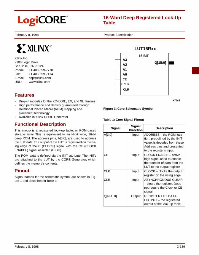
16-Word Deep Registered Look-Up Table
February 8, 1998 Product Specification
Xilinx Inc.2100 Logic DriveSan Jose, CA 95124Phone: +1 408-559-7778Fax: +1 408-559-7114E-mail: [email protected]: www.xilinx.com
R
Features• Drop-in modules for the XC4000E, EX, and XL families• High performance and density guaranteed through
Relational Placed Macro (RPM) mapping and placement technology
• Available in Xilinx CORE Generator
Functional DescriptionThis macro is a registered look-up table, or ROM-basedstorage array. This is equivalent to an N-bit wide, 16-bitdeep ROM. The address pins, A[3:0], are used to addressthe LUT data. The output of the LUT is registered on the ris-ing edge of the C (CLOCK) signal with the CE (CLOCKENABLE) signal asserted (HIGH).
The ROM data is defined via the INIT attribute. The INITsare attached to the LUT by the CORE Generator, whichdefines the memory’s contents.
PinoutSignal names for the schematic symbol are shown in Fig-ure 1 and described in Table 1.
Figure 1: Core Schematic Symbol
Table 1: Core Signal Pinout
Signal Signal
DirectionDescription
A[3:0] Input ADDRESS – the ROM loca-tion, predefined by the INIT value, is decoded from these Address pins and presented to the register’s input
CE Input CLOCK ENABLE – active high signal used to enable the transfer of data from the LUT to the output register
CLK Input CLOCK – clocks the output register on the rising edge
CLR Input ASYNCHRONOUS CLEAR – clears the register. Does not require the Clock or CE signal
Q[N-1, 0] Output REGISTER LUT DATA OUTPUT – the registered output of the look-up table
LUT16Rxx
X7548
CE
CLK
16 BITA3
Q[15:0]
A1A0
A2
CLR
February 8, 1998 2-139
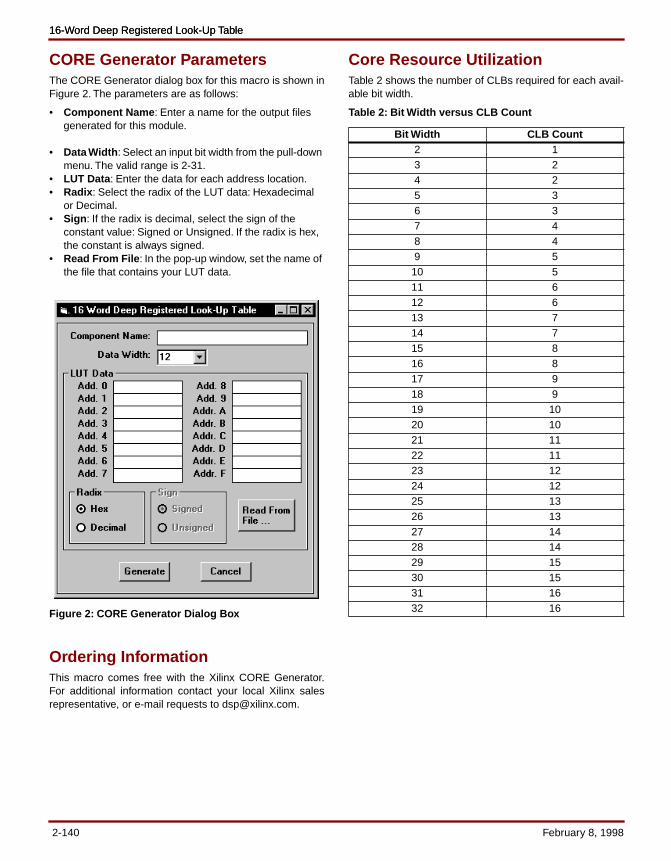
16-Word Deep Registered Look-Up Table16-Word Deep Registered Look-Up Table
CORE Generator ParametersThe CORE Generator dialog box for this macro is shown inFigure 2. The parameters are as follows:
• Component Name : Enter a name for the output files generated for this module.
• Data Width : Select an input bit width from the pull-down menu. The valid range is 2-31.
• LUT Data : Enter the data for each address location.• Radix : Select the radix of the LUT data: Hexadecimal
or Decimal.• Sign : If the radix is decimal, select the sign of the
constant value: Signed or Unsigned. If the radix is hex, the constant is always signed.
• Read From File : In the pop-up window, set the name of the file that contains your LUT data.
Figure 2: CORE Generator Dialog Box
Ordering InformationThis macro comes free with the Xilinx CORE Generator.For additional information contact your local Xilinx salesrepresentative, or e-mail requests to [email protected].
Core Resource UtilizationTable 2 shows the number of CLBs required for each avail-able bit width.
Table 2: Bit Width versus CLB Count Bit Width CLB Count
2 13 24 25 36 37 48 49 5
10 511 612 613 714 715 816 817 918 919 1020 1021 1122 1123 1224 1225 1326 1327 1428 1429 1530 1531 1632 16
2-140 February 8, 1998
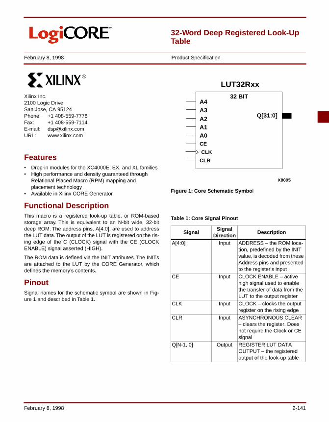
32-Word Deep Registered Look-Up Table
February 8, 1998 Product Specification
Xilinx Inc.2100 Logic DriveSan Jose, CA 95124Phone: +1 408-559-7778Fax: +1 408-559-7114E-mail: [email protected]: www.xilinx.com
R
Features• Drop-in modules for the XC4000E, EX, and XL families• High performance and density guaranteed through
Relational Placed Macro (RPM) mapping and placement technology
• Available in Xilinx CORE Generator
Functional DescriptionThis macro is a registered look-up table, or ROM-basedstorage array. This is equivalent to an N-bit wide, 32-bitdeep ROM. The address pins, A[4:0], are used to addressthe LUT data. The output of the LUT is registered on the ris-ing edge of the C (CLOCK) signal with the CE (CLOCKENABLE) signal asserted (HIGH).
The ROM data is defined via the INIT attributes. The INITsare attached to the LUT by the CORE Generator, whichdefines the memory’s contents.
PinoutSignal names for the schematic symbol are shown in Fig-ure 1 and described in Table 1.
Figure 1: Core Schematic Symbo l
Table 1: Core Signal Pinout
Signal Signal
DirectionDescription
A[4:0] Input ADDRESS – the ROM loca-tion, predefined by the INIT value, is decoded from these Address pins and presented to the register’s input
CE Input CLOCK ENABLE – active high signal used to enable the transfer of data from the LUT to the output register
CLK Input CLOCK – clocks the output register on the rising edge
CLR Input ASYNCHRONOUS CLEAR – clears the register. Does not require the Clock or CE signal
Q[N-1, 0] Output REGISTER LUT DATA OUTPUT – the registered output of the look-up table
LUT32Rxx
X8095
CE
CLK
32 BITA4A3
Q[31:0]
A1A0
A2
CLR
February 8, 1998 2-141
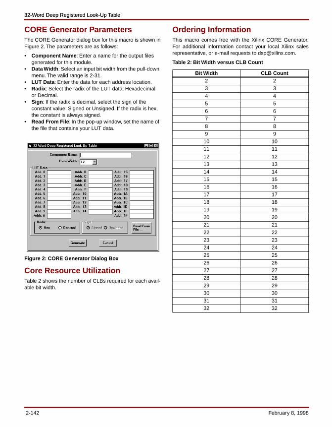
32-Word Deep Registered Look-Up Table32-Word Deep Registered Look-Up Table
CORE Generator ParametersThe CORE Generator dialog box for this macro is shown inFigure 2. The parameters are as follows:
• Component Name : Enter a name for the output files generated for this module.
• Data Width : Select an input bit width from the pull-down menu. The valid range is 2-31.
• LUT Data : Enter the data for each address location.• Radix : Select the radix of the LUT data: Hexadecimal
or Decimal.• Sign : If the radix is decimal, select the sign of the
constant value: Signed or Unsigned. If the radix is hex, the constant is always signed.
• Read From File : In the pop-up window, set the name of the file that contains your LUT data.
Figure 2: CORE Generator Dialog Box
Core Resource UtilizationTable 2 shows the number of CLBs required for each avail-able bit width.
Ordering InformationThis macro comes free with the Xilinx CORE Generator.For additional information contact your local Xilinx salesrepresentative, or e-mail requests to [email protected].
Table 2: Bit Width versus CLB Count
Bit Width CLB Count2 23 34 45 56 67 78 89 9
10 1011 1112 1213 1314 1415 1516 1617 1718 1819 1920 2021 2122 2223 2324 2425 2526 2627 2728 2829 2930 3031 3132 32
2-142 February 8, 1998
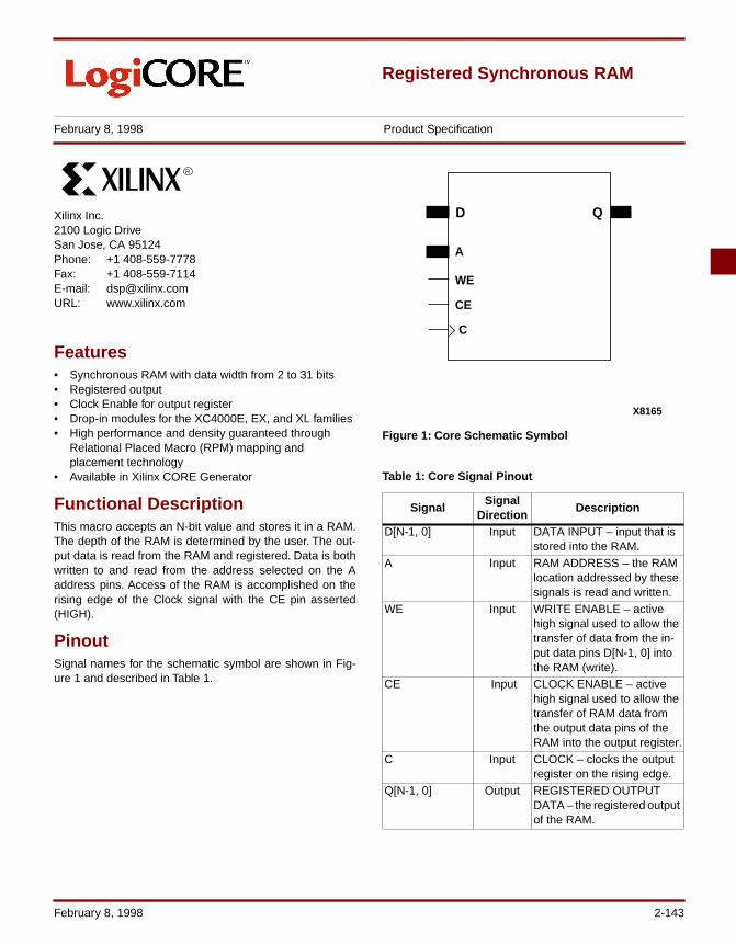
Registered Synchronous RAM
February 8, 1998 Product Specification
Xilinx Inc.2100 Logic DriveSan Jose, CA 95124Phone: +1 408-559-7778Fax: +1 408-559-7114E-mail: [email protected]: www.xilinx.com
R
Features• Synchronous RAM with data width from 2 to 31 bits• Registered output• Clock Enable for output register• Drop-in modules for the XC4000E, EX, and XL families• High performance and density guaranteed through
Relational Placed Macro (RPM) mapping and placement technology
• Available in Xilinx CORE Generator
Functional DescriptionThis macro accepts an N-bit value and stores it in a RAM.The depth of the RAM is determined by the user. The out-put data is read from the RAM and registered. Data is bothwritten to and read from the address selected on the Aaddress pins. Access of the RAM is accomplished on therising edge of the Clock signal with the CE pin asserted(HIGH).
PinoutSignal names for the schematic symbol are shown in Fig-ure 1 and described in Table 1.
Figure 1: Core Schematic Symbol
Table 1: Core Signal Pinout
SignalSignal
DirectionDescription
D[N-1, 0] Input DATA INPUT – input that is stored into the RAM.
A Input RAM ADDRESS – the RAM location addressed by these signals is read and written.
WE Input WRITE ENABLE – active high signal used to allow the transfer of data from the in-put data pins D[N-1, 0] into the RAM (write).
CE Input CLOCK ENABLE – active high signal used to allow the transfer of RAM data from the output data pins of the RAM into the output register.
C Input CLOCK – clocks the output register on the rising edge.
Q[N-1, 0] Output REGISTERED OUTPUT DATA – the registered output of the RAM.
X8165
A
CE
D
C
WE
Q
February 8, 1998 2-143
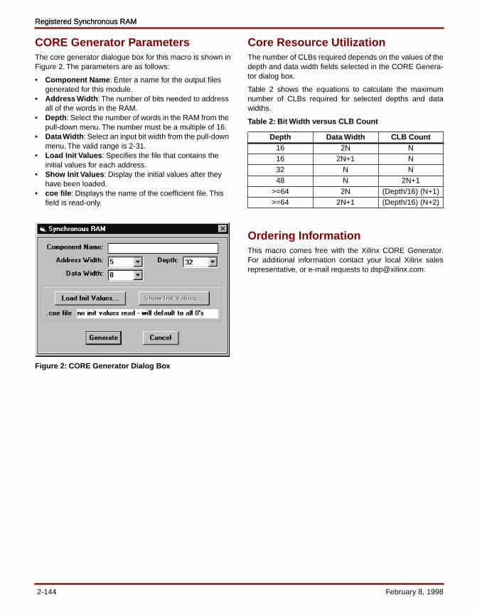
Registered Synchronous RAMRegistered Synchronous RAM
CORE Generator ParametersThe core generator dialogue box for this macro is shown inFigure 2. The parameters are as follows:
• Component Name : Enter a name for the output files generated for this module.
• Address Width : The number of bits needed to address all of the words in the RAM.
• Depth : Select the number of words in the RAM from the pull-down menu. The number must be a multiple of 16.
• Data Width : Select an input bit width from the pull-down menu. The valid range is 2-31.
• Load Init Values : Specifies the file that contains the initial values for each address.
• Show Init Values : Display the initial values after they have been loaded.
• coe file : Displays the name of the coefficient file. This field is read-only.
Figure 2: CORE Generator Dialog Box
Core Resource UtilizationThe number of CLBs required depends on the values of thedepth and data width fields selected in the CORE Genera-tor dialog box.
Table 2 shows the equations to calculate the maximumnumber of CLBs required for selected depths and datawidths.
Table 2: Bit Width versus CLB Count
Ordering InformationThis macro comes free with the Xilinx CORE Generator.For additional information contact your local Xilinx salesrepresentative, or e-mail requests to [email protected].
Depth Data Width CLB Count16 2N N16 2N+1 N32 N N48 N 2N+1
>=64 2N (Depth/16) (N+1)>=64 2N+1 (Depth/16) (N+2)
2-144 February 8, 1998
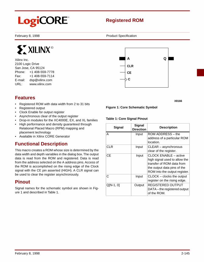
Registered ROM
February 8, 1998 Product Specification
Xilinx Inc.2100 Logic DriveSan Jose, CA 95124Phone: +1 408-559-7778Fax: +1 408-559-7114E-mail: [email protected]: www.xilinx.com
R
Features• Registered ROM with data width from 2 to 31 bits• Registered output• Clock Enable for output register• Asynchronous clear of the output register • Drop-in modules for the XC4000E, EX, and XL families• High performance and density guaranteed through
Relational Placed Macro (RPM) mapping and placement technology
• Available in Xilinx CORE Generator
Functional DescriptionThis macro creates a ROM whose size is determined by thedata width and depth variables in the dialog box. The outputdata is read from the ROM and registered. Data is readfrom the address selected on the A address pins. Access ofthe ROM is accomplished on the rising edge of the Clocksignal with the CE pin asserted (HIGH). A CLR signal canbe used to clear the register asynchronously.
PinoutSignal names for the schematic symbol are shown in Fig-ure 1 and described in Table 1.
Figure 1: Core Schematic Symbol
Table 1: Core Signal Pinout
SignalSignal
DirectionDescription
A Input ROM ADDRESS – the address of a particular ROM location.
CLR Input CLEAR – asynchronous clear of the register.
CE Input CLOCK ENABLE – active high signal used to allow the transfer of ROM data from the output data pins of the ROM into the output register.
C Input CLOCK – clocks the output register on the rising edge.
Q[N-1, 0] Output REGISTERED OUTPUT DATA – the registered output of the ROM.
X8166
CE
A
C
CLR
Q
February 8, 1998 2-145
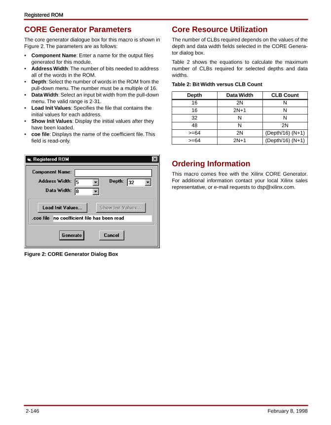
Registered ROMRegistered ROM
CORE Generator ParametersThe core generator dialogue box for this macro is shown inFigure 2. The parameters are as follows:
• Component Name : Enter a name for the output files generated for this module.
• Address Width : The number of bits needed to address all of the words in the ROM.
• Depth : Select the number of words in the ROM from the pull-down menu. The number must be a multiple of 16.
• Data Width : Select an input bit width from the pull-down menu. The valid range is 2-31.
• Load Init Values : Specifies the file that contains the initial values for each address.
• Show Init Values : Display the initial values after they have been loaded.
• coe file : Displays the name of the coefficient file. This field is read-only.
Figure 2: CORE Generator Dialog Box
Core Resource UtilizationThe number of CLBs required depends on the values of thedepth and data width fields selected in the CORE Genera-tor dialog box.
Table 2 shows the equations to calculate the maximumnumber of CLBs required for selected depths and datawidths.
Table 2: Bit Width versus CLB Count
Ordering InformationThis macro comes free with the Xilinx CORE Generator.For additional information contact your local Xilinx salesrepresentative, or e-mail requests to [email protected].
Depth Data Width CLB Count16 2N N16 2N+1 N32 N N48 N 2N
>=64 2N (Depth/16) (N+1)>=64 2N+1 (Depth/16) (N+1)
2-146 February 8, 1998
AllianceCORE Products
AllianceCORE Products
1. Introduction
2. LogiCORE Products
3. AllianceCORE Products
4. LogiBLOX
5. Reference Designs
3-1
AllianceCORE Products Table of Contents
February 8, 1998
AllianceCORE ProductsAllianceCORE Program Overview . . . . . . . . . . . . . . . . . . . . . . . . . . . . . . . . . . . . . .3-5
Standard Bus Interface Products Table of Contents . . . . . . . . . . . . . . . . . . . . . . . .3-7XF-TWSI Two-Wire Serial Interface . . . . . . . . . . . . . . . . . . . . . . . . . . . . . . . . . . . . .3-9PCMCIA Fax/Modem Macro . . . . . . . . . . . . . . . . . . . . . . . . . . . . . . . . . . . . . . . . .3-15PCMCIA Library R1.2 . . . . . . . . . . . . . . . . . . . . . . . . . . . . . . . . . . . . . . . . . . . . . . .3-19PCMCIA Prototyping Card . . . . . . . . . . . . . . . . . . . . . . . . . . . . . . . . . . . . . . . . . . .3-23PCMCIA Card Debugger/Exerciser . . . . . . . . . . . . . . . . . . . . . . . . . . . . . . . . . . . .3-25PCMCIA CIS Generator 1.2 . . . . . . . . . . . . . . . . . . . . . . . . . . . . . . . . . . . . . . . . . .3-27Low-Speed USB Function Controller . . . . . . . . . . . . . . . . . . . . . . . . . . . . . . . . . . .3-29Full-Speed USB Function Controller . . . . . . . . . . . . . . . . . . . . . . . . . . . . . . . . . . .3-333-Port USB Hub Controller . . . . . . . . . . . . . . . . . . . . . . . . . . . . . . . . . . . . . . . . . . .3-37USB Function Evaluation Board . . . . . . . . . . . . . . . . . . . . . . . . . . . . . . . . . . . . . . .3-41USB Hub Evaluation Board . . . . . . . . . . . . . . . . . . . . . . . . . . . . . . . . . . . . . . . . . .3-43USB Simulation Model . . . . . . . . . . . . . . . . . . . . . . . . . . . . . . . . . . . . . . . . . . . . . .3-45
Communications and Networking Products Table of Contents . . . . . . . . . . . . . .3-47Cell Assembler (CC-201) . . . . . . . . . . . . . . . . . . . . . . . . . . . . . . . . . . . . . . . . . . . .3-49Cell Delineation (CC-200) . . . . . . . . . . . . . . . . . . . . . . . . . . . . . . . . . . . . . . . . . . .3-53CRC10 Generator and Verifier (CC-130) . . . . . . . . . . . . . . . . . . . . . . . . . . . . . . . .3-57CRC32 Generator and Verifier (CC-131) . . . . . . . . . . . . . . . . . . . . . . . . . . . . . . . .3-61HDLC Protocol Core . . . . . . . . . . . . . . . . . . . . . . . . . . . . . . . . . . . . . . . . . . . . . . .3-65Reed-Solomon Decoder . . . . . . . . . . . . . . . . . . . . . . . . . . . . . . . . . . . . . . . . . . . . 3-71Reed-Solomon Encoder . . . . . . . . . . . . . . . . . . . . . . . . . . . . . . . . . . . . . . . . . . . . 3-77MT1F T1 Framer . . . . . . . . . . . . . . . . . . . . . . . . . . . . . . . . . . . . . . . . . . . . . . . . . .3-81UTOPIA Slave (CC-141) . . . . . . . . . . . . . . . . . . . . . . . . . . . . . . . . . . . . . . . . . . . .3-85Viterbi Decoder . . . . . . . . . . . . . . . . . . . . . . . . . . . . . . . . . . . . . . . . . . . . . . . . . . .3-91
Processor Products Table of Contents . . . . . . . . . . . . . . . . . . . . . . . . . . . . . . . . . .3-95TX400 Series RISC CPU Cores . . . . . . . . . . . . . . . . . . . . . . . . . . . . . . . . . . . . . . .3-97RISC CPU Core Design Base Board . . . . . . . . . . . . . . . . . . . . . . . . . . . . . . . . . .3-103Scalable Development Platform Integrated Software . . . . . . . . . . . . . . . . . . . . .3-107V8-uRISC 8-bit RISC Microprocessor . . . . . . . . . . . . . . . . . . . . . . . . . . . . . . . . .3-109IntelliCore‘ Prototyping System. . . . . . . . . . . . . . . . . . . . . . . . . . . . . . . . . . . . . . 3-115
Processor Peripherals Table of Contents . . . . . . . . . . . . . . . . . . . . . . . . . . . . . . .3-119M16450 Universal Asynchronous Receiver/Transmitter . . . . . . . . . . . . . . . . . . .3-121M16550A - Universal Asynchronous Receiver/Transmitter With FIFOs . . . . . . . .3-125C2910A Microprogram Controller . . . . . . . . . . . . . . . . . . . . . . . . . . . . . . . . . . . . 3-129M8237 DMA Controller . . . . . . . . . . . . . . . . . . . . . . . . . . . . . . . . . . . . . . . . . . . . 3-133XF8250 Asynchronous Communications Core . . . . . . . . . . . . . . . . . . . . . . . . . . 3-137M8254 Programmable Timer . . . . . . . . . . . . . . . . . . . . . . . . . . . . . . . . . . . . . . . 3-143M8255 Programmable Peripheral Interface . . . . . . . . . . . . . . . . . . . . . . . . . . . . .3-147XF8255 Programmable Peripheral Interface . . . . . . . . . . . . . . . . . . . . . . . . . . . .3-151
3-2 February 8, 1998
XF8256 Multifunction Microprocessor Support Controller . . . . . . . . . . . . . . . . . .3-155M8259 Programmable Interrupt Controller . . . . . . . . . . . . . . . . . . . . . . . . . . . . . .3-159XF8279 Programmable Keyboard Display Interface . . . . . . . . . . . . . . . . . . . . . .3-163XF9128 Video Terminal Logic Controller . . . . . . . . . . . . . . . . . . . . . . . . . . . . . . .3-167DRAM Controller . . . . . . . . . . . . . . . . . . . . . . . . . . . . . . . . . . . . . . . . . . . . . . . . .3-173
General Core Development Tools Table of Contents . . . . . . . . . . . . . . . . . . . . . .3-177GVA-100 DSP Prototyping Platform . . . . . . . . . . . . . . . . . . . . . . . . . . . . . . . . . .3-179MDS FPGA Development Module . . . . . . . . . . . . . . . . . . . . . . . . . . . . . . . . . . . .3-183Microprocessor Based Core Evaluation Card . . . . . . . . . . . . . . . . . . . . . . . . . . .3-185
AllianceCORE Partner Profiles Table of Contents . . . . . . . . . . . . . . . . . . . . . . . .3-189Partner Profiles Overview . . . . . . . . . . . . . . . . . . . . . . . . . . . . . . . . . . . . . . . . . .3-191CAST, Inc. . . . . . . . . . . . . . . . . . . . . . . . . . . . . . . . . . . . . . . . . . . . . . . . . . . . . . .3-193Comit Systems, Inc. . . . . . . . . . . . . . . . . . . . . . . . . . . . . . . . . . . . . . . . . . . . . . . .3-195CoreEl MicroSystems . . . . . . . . . . . . . . . . . . . . . . . . . . . . . . . . . . . . . . . . . . . . . .3-196DeDris Embedded Algorithms BV . . . . . . . . . . . . . . . . . . . . . . . . . . . . . . . . . . . .3-198Digital Objects, Corporation . . . . . . . . . . . . . . . . . . . . . . . . . . . . . . . . . . . . . . . . .3-200Eureka Technology, Inc. . . . . . . . . . . . . . . . . . . . . . . . . . . . . . . . . . . . . . . . . . . .3-201GV & Associates, Inc. . . . . . . . . . . . . . . . . . . . . . . . . . . . . . . . . . . . . . . . . . . . . .3-202Innovative Semiconductors, Inc. . . . . . . . . . . . . . . . . . . . . . . . . . . . . . . . . . . . . .3-203Integrated Silicon Systems, Ltd. . . . . . . . . . . . . . . . . . . . . . . . . . . . . . . . . . . . . . .3-204Logic Innovations, Inc. . . . . . . . . . . . . . . . . . . . . . . . . . . . . . . . . . . . . . . . . . . . . .3-206Memec Design Services . . . . . . . . . . . . . . . . . . . . . . . . . . . . . . . . . . . . . . . . . . .3-208Mentor Graphics Corporation . . . . . . . . . . . . . . . . . . . . . . . . . . . . . . . . . . . . . . . .3-210Mobile Media Research, Inc. . . . . . . . . . . . . . . . . . . . . . . . . . . . . . . . . . . . . . . . .3-213NMI Electronics Ltd. . . . . . . . . . . . . . . . . . . . . . . . . . . . . . . . . . . . . . . . . . . . . . . .3-215Perigee, LLC . . . . . . . . . . . . . . . . . . . . . . . . . . . . . . . . . . . . . . . . . . . . . . . . . . . .3-216Phoenix Technologies/Virtual Chips . . . . . . . . . . . . . . . . . . . . . . . . . . . . . . . . . . 3-217Rice Electronics . . . . . . . . . . . . . . . . . . . . . . . . . . . . . . . . . . . . . . . . . . . . . . . . . .3-218Sand Microelectronics . . . . . . . . . . . . . . . . . . . . . . . . . . . . . . . . . . . . . . . . . . . . .3-219SICAN Microelectronics Corp. . . . . . . . . . . . . . . . . . . . . . . . . . . . . . . . . . . . . . . .3-220T7L Technology, Inc. . . . . . . . . . . . . . . . . . . . . . . . . . . . . . . . . . . . . . . . . . . . . . .3-221Technology Rendezvous Inc. . . . . . . . . . . . . . . . . . . . . . . . . . . . . . . . . . . . . . . . .3-222VAutomation . . . . . . . . . . . . . . . . . . . . . . . . . . . . . . . . . . . . . . . . . . . . . . . . . . . . .3-223Virtual IP Group, Inc. . . . . . . . . . . . . . . . . . . . . . . . . . . . . . . . . . . . . . . . . . . . . . .3-225
February 8, 1998 3-3
AllianceCORE Products Table of Contents
3-4 February 8, 1998

AllianceCORE Program Overview
February 8, 1998
DescriptionThe AllianceCORE program is a cooperative effort betweenXilinx and independent third-party core developers. It isdesigned to produce a broad selection of industry-standardsolutions dedicated for use in Xilinx programmable logic.
Xilinx takes an active role with its partners in the process ofproductizing AllianceCOREs. This is unique to the Alli-anceCORE program. Because the process is so involved,we work closely with our partners to select the right coresfirst which helps raise the quality and usability of the coresthat are offered.
AllianceCORE CriteriaA core must meet a minimum set of criteria before it canreceive the AllianceCORE label.
Core SelectionXilinx looks at cores from a practical point of view. A pro-grammable logic version of a core must have value over anASIC or standard product version of the same function. Itmust be cost effective and make sense for use in a pro-grammable device in a production system. If a candidatecore does not pass these simple tests, then it does notmake sense to invest the effort to convert it to an Alli-anceCORE product.
Core QualificationGeneric, synthesizable cores offer maximum flexibility forusers with unique requirements. This is typically the formatfor cores provided to the ASIC market.
With programmable logic, however, this flexibility can comeat the expense of efficiency and performance. It can takeconsiderable effort to get a core to synthesize in a way thatmeets density and timing requirements. Time spent tryingto accomplish this quickly reduces the time-to-marketadvantage of using programmable logic and cores in thefirst place.
As a result, Xilinx is does not promote generic, synthesiz-able cores as AllianceCORE products. Instead, they aregenerally provided as black-boxes that allow customizationin critical areas. This guarantees that the implementation isoptimized for density while still meeting performance, pre-serving the time-to-market value of programmable logic.
Flexibility is provided by allowing you to quickly implementyour unique logic on the same device. Source code ver-
sions of the cores are often available from the partners atadditional cost for those who need ultimate flexibility.
Announced AllianceCORE products have been imple-mented and verified in a Xilinx device. They are availableimmediately for purchase in a Xilinx netlist format such as.xnf or .ngd and are usable in either the Xilinx Alliance orFoundation series development software. When required,the cores also come with appropriate constraints files toguarantee functionality and critical timing. In all cases thepartner is responsible for guaranteeing the operation of thefunction itself.
AllianceCORE products originated from either schematic orHDL entry tools.
Core IntegrationAllianceCORE products are not just cores. They are com-plete solutions for system designs. While cores by them-selves have value, in many cases it is often not enough tojust supply the core. You need tools such as system soft-ware and prototyping boards to help you rapidly integratethe core into your design, perform system debug in a real-world environment, and then quickly convert the prototypeto a production unit. This is particularly true of complexfunctions.
Many AllianceCORE functions are supported by Xilinx-based demonstration or prototyping boards. Some alsohave system simulation models or development software.This allows you to evaluate and work with the functionbefore you have to layout your board.
These tools are provided by the AllianceCORE partner,usually at additional cost. Descriptions of available supporttools for each core are included in this data book.
Complete solutions like these help preserve the value ofusing programmable logic while lowering the support bur-den for the core provider.
Acquiring AllianceCORE ProductsAllianceCORE products are sold and serviced directly bythe AllianceCORE partners since they are the experts fortheir particular products. They are responsible for pricing,licensing terms, delivery and technical support. Contactinformation for each partner is included in the Alli-anceCORE Partner Profiles section of this data book.
If you want additional information about the AllianceCOREprogram or are interested in becoming a partner, contactXilinx directly.
February 8, 1998 3-5
AllianceCORE Program Overview
Xilinx, Inc.2100 Logic DriveSan Jose, CA 95124Attn: CORE Solutions GroupPhone: 408-879-5381Fax: 408-377-3259
E-mail: [email protected]: www.xilinx.com/products/logicore
/alliance/tblpart.htm
3-6 February 8, 1998
Standard Bus Interface Products Table of Contents
February 8, 1998
XF-TWSI Two-Wire Serial Interface . . . . . . . . . . . . . . . . . . . . . . . . . . . . . . . . . . . . .3-9PCMCIA Fax/Modem Macro . . . . . . . . . . . . . . . . . . . . . . . . . . . . . . . . . . . . . . . . .3-15PCMCIA Library R1.2 . . . . . . . . . . . . . . . . . . . . . . . . . . . . . . . . . . . . . . . . . . . . . . .3-19PCMCIA Prototyping Card . . . . . . . . . . . . . . . . . . . . . . . . . . . . . . . . . . . . . . . . . . .3-23PCMCIA Card Debugger/Exerciser . . . . . . . . . . . . . . . . . . . . . . . . . . . . . . . . . . . .3-25PCMCIA CIS Generator 1.2 . . . . . . . . . . . . . . . . . . . . . . . . . . . . . . . . . . . . . . . . . .3-27Low-Speed USB Function Controller . . . . . . . . . . . . . . . . . . . . . . . . . . . . . . . . . . .3-29Full-Speed USB Function Controller . . . . . . . . . . . . . . . . . . . . . . . . . . . . . . . . . . .3-333-Port USB Hub Controller . . . . . . . . . . . . . . . . . . . . . . . . . . . . . . . . . . . . . . . . . . .3-37USB Function Evaluation Board . . . . . . . . . . . . . . . . . . . . . . . . . . . . . . . . . . . . . . .3-41USB Hub Evaluation Board . . . . . . . . . . . . . . . . . . . . . . . . . . . . . . . . . . . . . . . . . .3-43USB Simulation Model . . . . . . . . . . . . . . . . . . . . . . . . . . . . . . . . . . . . . . . . . . . . . .3-45
3-7 February 8, 1998

Standard Bus Interface Products Table of Contents
3-8 February 8, 1998
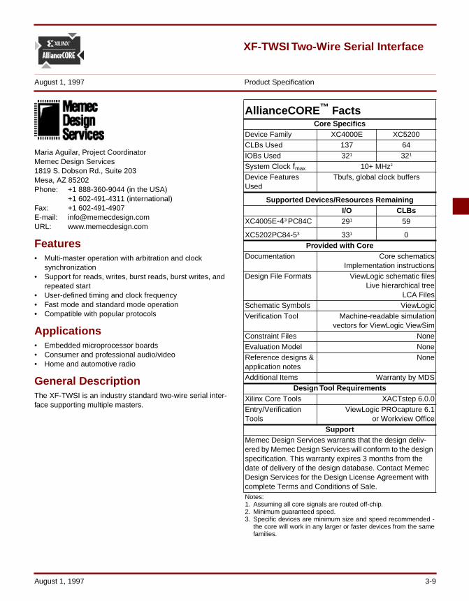
August 1, 1997 Product Specification
XF-TWSI Two-Wire Serial Interface
Maria Aguilar, Project CoordinatorMemec Design Services1819 S. Dobson Rd., Suite 203Mesa, AZ 85202Phone: +1 888-360-9044 (in the USA)
+1 602-491-4311 (international)Fax: +1 602-491-4907E-mail: [email protected]: www.memecdesign.com
Features• Multi-master operation with arbitration and clock
synchronization• Support for reads, writes, burst reads, burst writes, and
repeated start• User-defined timing and clock frequency• Fast mode and standard mode operation• Compatible with popular protocols
Applications• Embedded microprocessor boards • Consumer and professional audio/video• Home and automotive radio
General DescriptionThe XF-TWSI is an industry standard two-wire serial inter-face supporting multiple masters.
AllianceCORE ™ FactsCore Specifics
Device Family XC4000E XC5200CLBs Used 137 64IOBs Used 321 321
System Clock fmax 10+ MHz2
Device Features Used
Tbufs, global clock buffers
Supported Devices/Resources RemainingI/O CLBs
XC4005E-43 PC84C 291 59
XC5202PC84-53 331 0Provided with Core
Documentation Core schematicsImplementation instructions
Design File Formats ViewLogic schematic filesLive hierarchical tree
LCA FilesSchematic Symbols ViewLogicVerification Tool Machine-readable simulation
vectors for ViewLogic ViewSimConstraint Files NoneEvaluation Model NoneReference designs & application notes
None
Additional Items Warranty by MDSDesign Tool Requirements
Xilinx Core Tools XACTstep 6.0.0Entry/Verification Tools
ViewLogic PROcapture 6.1or Workview Office
SupportMemec Design Services warrants that the design deliv-ered by Memec Design Services will conform to the design specification. This warranty expires 3 months from the date of delivery of the design database. Contact Memec Design Services for the Design License Agreement with complete Terms and Conditions of Sale.Notes:1. Assuming all core signals are routed off-chip.2. Minimum guaranteed speed.3. Specific devices are minimum size and speed recommended -
the core will work in any larger or faster devices from the samefamilies.
August 1, 1997 3-9
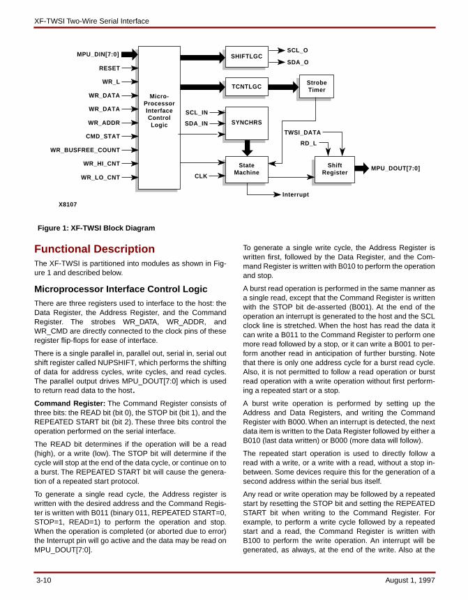
XF-TWSI Two-Wire Serial Interface
Functional DescriptionThe XF-TWSI is partitioned into modules as shown in Fig-ure 1 and described below.
Microprocessor Interface Control LogicThere are three registers used to interface to the host: theData Register, the Address Register, and the CommandRegister. The strobes WR_DATA, WR_ADDR, andWR_CMD are directly connected to the clock pins of theseregister flip-flops for ease of interface.
There is a single parallel in, parallel out, serial in, serial outshift register called NUPSHIFT, which performs the shiftingof data for address cycles, write cycles, and read cycles.The parallel output drives MPU_DOUT[7:0] which is usedto return read data to the host.Command Register: The Command Register consists ofthree bits: the READ bit (bit 0), the STOP bit (bit 1), and theREPEATED START bit (bit 2). These three bits control theoperation performed on the serial interface.
The READ bit determines if the operation will be a read(high), or a write (low). The STOP bit will determine if thecycle will stop at the end of the data cycle, or continue on toa burst. The REPEATED START bit will cause the genera-tion of a repeated start protocol.
To generate a single read cycle, the Address register iswritten with the desired address and the Command Regis-ter is written with B011 (binary 011, REPEATED START=0,STOP=1, READ=1) to perform the operation and stop.When the operation is completed (or aborted due to error)the Interrupt pin will go active and the data may be read onMPU_DOUT[7:0].
To generate a single write cycle, the Address Register iswritten first, followed by the Data Register, and the Com-mand Register is written with B010 to perform the operationand stop.
A burst read operation is performed in the same manner asa single read, except that the Command Register is writtenwith the STOP bit de-asserted (B001). At the end of theoperation an interrupt is generated to the host and the SCLclock line is stretched. When the host has read the data itcan write a B011 to the Command Register to perform onemore read followed by a stop, or it can write a B001 to per-form another read in anticipation of further bursting. Notethat there is only one address cycle for a burst read cycle.Also, it is not permitted to follow a read operation or burstread operation with a write operation without first perform-ing a repeated start or a stop.
A burst write operation is performed by setting up theAddress and Data Registers, and writing the CommandRegister with B000. When an interrupt is detected, the nextdata item is written to the Data Register followed by either aB010 (last data written) or B000 (more data will follow).
The repeated start operation is used to directly follow aread with a write, or a write with a read, without a stop in-between. Some devices require this for the generation of asecond address within the serial bus itself.
Any read or write operation may be followed by a repeatedstart by resetting the STOP bit and setting the REPEATEDSTART bit when writing to the Command Register. Forexample, to perform a write cycle followed by a repeatedstart and a read, the Command Register is written withB100 to perform the write operation. An interrupt will begenerated, as always, at the end of the write. Also at the
Figure 1: XF-TWSI Block Diagram
StrobeTimerTCNTLGC
SHIFTLGC
X8107
RESET
MPU_DIN[7:0]
WR_L
WR_DATA
WR_DATA
WR_ADDR
CMD_STAT
WR_BUSFREE_COUNT
WR_HI_CNT
WR_LO_CNT
Micro-ProcessorInterfaceControlLogic
StateMachine
ShiftRegister
SYNCHRS
SCL_IN
RD_L
TWSI_DATA
SCL_O
SDA_O
MPU_DOUT[7:0]
Interrupt
SDA_IN
CLK
3-10 August 1, 1997
Memec Design Services
end of the write the clock line (SCL) will be stretched untilthe new command is written. If a single read is desired theCommand Register is written with B011.
Timing: The primary clock, CLK, may be operated from 8to 16 MHz by changing the timing dividers onBUSFREE_COUNT, HI_COUNT, and LO_COUNT corepins. These three bussed pins are used to define the timingfor the part by attaching the appropriate divider values.These divider values are multiplexed into a counter which isused to time the low and high width of the SCL clock, thesetup time and hold times, and the “bus free” time for arbi-tration purposes.
The BUSFREE_COUNT value is used to set the bus freetime in terms of CLK periods. The XF-TWSI must see boththe SDA and SCL pins in a high state for the bus free periodbefore it issues a start or repeated start command on thebus. Note that this value must be set greater than the long-est SCL high period in the system for arbitration to functionproperly. For Standard mode devices this should be set toat least 5 microseconds. For Fast mode devices this shouldbe set to at least 1.5 microseconds.
The HI_COUNT value is used to define the low period ofthe SCL clock and the setup time for a repeated start com-mand (rising edge of SCL to falling edge of SDA). Thisvalue is generally set to 4.7 microseconds for Standardmode and 1.3 microseconds for Fast mode.
The LO_COUNT value is used to define the high width ofthe SCL clock, the setup time for a stop command (risingedge of SCL to rising edge of SDA), as well as the startcommand hold time (falling edge of SDA to falling edge ofSCL). This value is generally set to 4.0 microseconds forStandard mode and .6 microseconds for Fast mode.
The values can be added to busses attached to these pinsas a series of VCCs and GNDs.Note that the actual valuesobtained from these dividers will be slightly larger due tostate machine overhead.
SYNCHRS Block
The SDA and SCL inputs are passed through this modulethat performs a dual-rank synchronization and glitch filter-ing when enabled by the FILTER_EN signal. The synchro-nized versions of the SDA and SCL signals are used in allcore modules.
The XF-TWSI core treats both the SDA and SCL lines asdata lines. The SDA line is actually sampled some numberof clocks after the rising edge of SCL is detected. Thisallows for greater noise immunity and more robust opera-tion.
State Machine Block
The control for the serial interface comes from theTWSI_SM state machine. This state machine controls theloading and enabling of all shift registers and counters, andis responsible for implementing the basic interface protocol.
Arbitration: Before the XF-TWSI issues either a start orrepeated start command it samples the synchronized ver-sions of SDA and SCL for BUSFREE_COUNT x clock peri-ods of high values. If at any time either of these pins isdetected in a low (driven) state then the count starts over (itassumes that another master is on the bus). The automaticretrying to obtain the serial bus only occurs until the startcommand is issued. After that the responsibility of the retryis left to software, since cycles may be of infinite length.
After a start is issued and while the address or data is beingwritten to the slave, the core samples the data on the SDApin while SCL is high. If a data mismatch is detected thenthe operation is aborted with an interrupt and a BUSLOSSstatus. This can also occur during burst reads whenever aNACK is intended to be issued and an ACK is detectedinstead.
Performing Basic Cycles: The interface between the hostand the XF-TWSI is interrupt-based. The host sets up theAddress and Data Registers, writes the Command Registerto initiate the desired operation, and performs other opera-tions until the interrupt is generated by the core. Alterna-tively, if polled operation is desired, the Status Register maybe read to see if the interrupt line is active.
Upon receiving the interrupt the host must read the StatusRegister to see if either of the two error conditions ispresent. Bit 2 in the Status Register is BUSLOSS, whichoccurs if the interface lost the bus to another master beforecompletion of the cycle. Bit 1 in the Status Register is STA-TUS TIMEOUT, which occurs if the slave does not respondwith an acknowledge when required. For either of theseerror conditions the host must retry the current cycle upuntil the last interrupt. Note that for burst operations thehost is responsible for writing the incremented address intothe Address Register before retrying the operation.
After the host receives the interrupt and determines the sta-tus, it sets up the registers again and writes the CommandRegister to start the next cycle. The act of writing the Com-mand Register clears out the current interrupt.
Shift Logic (SHIFTLGC)
The basic cycle on theXF-TWSI serial interface consists ofan address cycle followed by a data cycle. The addressconsists of seven bits and the read/write bit (the LSB). TheMSB is always transmitted first on the SDA line. The datacycle can either be a read or a write. For a write operationthe XF-IIC shifts the data from the Data Register onto theSDA line. For a read operation the core captures the datainto the shift register. The data cycle can end in three differ-ent ways:
1. A stop can be generated which terminates the currentcycle.
2. Another data cycle can take place (a burst).
3. A repeated start can be generated by the interface.
August 1, 1997 3-11
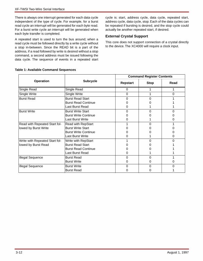
XF-TWSI Two-Wire Serial Interface
There is always one interrupt generated for each data cycleindependent of the type of cycle. For example, for a burstread cycle an interrupt will be generated for each byte read.For a burst write cycle an interrupt will be generated wheneach byte transfer is completed.
A repeated start is used to turn the bus around; when aread cycle must be followed directly by a write cycle withouta stop in-between. Since the READ bit is a part of theaddress, if a read followed by write is desired without a stopcommand, a second address must be issued following thedata cycle. The sequence of events in a repeated start
cycle is: start, address cycle, data cycle, repeated start,address cycle, data cycle, stop. Each of the data cycles canbe repeated if bursting is desired, and the stop cycle couldactually be another repeated start, if desired.
External Crystal Support
This core does not support connection of a crystal directlyto the device. The XC4000 will require a clock input.
Table 1: Available Command Sequences
Command Register ContentsOperation Subcycle Repstart Stop Read
Single Read Single Read 0 1 1Single Write Single Write 0 1 0Burst Read Burst Read Start
Burst Read ContinueLast Burst Read
000
001
111
Burst Write Burst Write StartBurst Write ContinueLast Burst Write
000
001
000
Read with Repeated Start fol-lowed by Burst Write
Read with RepStartBurst Write StartBurst Write ContinueLast Burst Write
1000
0001
1000
Write with Repeated Start fol-lowed by Burst Read
Write with RepStartBurst Read StartBurst Read ContinueLast Burst Read
1000
0001
0111
Illegal Sequence Burst ReadBurst Write
00
00
10
Illegal Sequence Burst WriteBurst Read
00
00
01
3-12 August 1, 1997
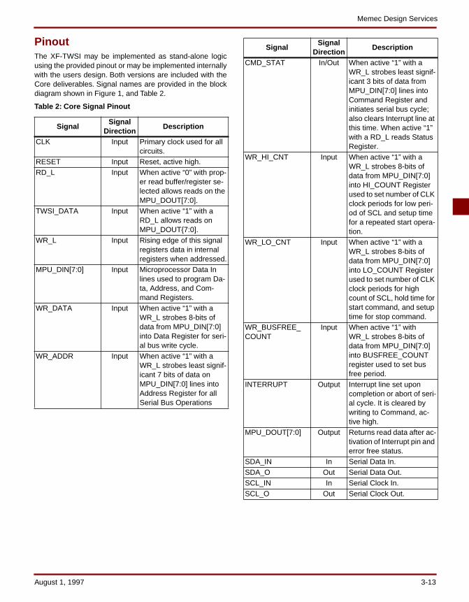
Memec Design Services
PinoutThe XF-TWSI may be implemented as stand-alone logicusing the provided pinout or may be implemented internallywith the users design. Both versions are included with theCore deliverables. Signal names are provided in the blockdiagram shown in Figure 1, and Table 2.
Table 2: Core Signal Pinout
SignalSignal
DirectionDescription
CLK Input Primary clock used for all circuits.
RESET Input Reset, active high.RD_L Input When active “0” with prop-
er read buffer/register se-lected allows reads on the MPU_DOUT[7:0].
TWSI_DATA Input When active “1” with a RD_L allows reads on MPU_DOUT{7:0].
WR_L Input Rising edge of this signal registers data in internal registers when addressed.
MPU_DIN[7:0] Input Microprocessor Data In lines used to program Da-ta, Address, and Com-mand Registers.
WR_DATA Input When active “1” with a WR_L strobes 8-bits of data from MPU_DIN[7:0] into Data Register for seri-al bus write cycle.
WR_ADDR Input When active “1” with a WR_L strobes least signif-icant 7 bits of data on MPU_DIN[7:0] lines into Address Register for all Serial Bus Operations
CMD_STAT In/Out When active “1” with a WR_L strobes least signif-icant 3 bits of data from MPU_DIN[7:0] lines into Command Register and initiates serial bus cycle; also clears Interrupt line at this time. When active “1” with a RD_L reads Status Register.
WR_HI_CNT Input When active “1” with a WR_L strobes 8-bits of data from MPU_DIN[7:0] into HI_COUNT Register used to set number of CLK clock periods for low peri-od of SCL and setup time for a repeated start opera-tion.
WR_LO_CNT Input When active “1” with a WR_L strobes 8-bits of data from MPU_DIN[7:0] into LO_COUNT Register used to set number of CLK clock periods for high count of SCL, hold time for start command, and setup time for stop command.
WR_BUSFREE_COUNT
Input When active “1” with WR_L strobes 8-bits of data from MPU_DIN[7:0] into BUSFREE_COUNT register used to set bus free period.
INTERRUPT Output Interrupt line set upon completion or abort of seri-al cycle. It is cleared by writing to Command, ac-tive high.
MPU_DOUT[7:0] Output Returns read data after ac-tivation of Interrupt pin and error free status.
SDA_IN In Serial Data In.SDA_O Out Serial Data Out.SCL_IN In Serial Clock In.SCL_O Out Serial Clock Out.
SignalSignal
DirectionDescription
August 1, 1997 3-13

XF-TWSI Two-Wire Serial Interface
Core ModificationsThe XF-TWSI meets or exceeds the industry standard.However, in most cases the Timespecs can be tightenedsignificantly. Successful operation with 120ns bus cycleshas been achieved. In all cases, a post-route timing analy-sis should be performed to verify performance. Implemen-tation beyond 10MHz and other customizing is availablethrough Memec Design Services.
Verification MethodsComplete functional and timing simulation has been per-formed on the XF-TWSI using Viewsim. (Simulation vectorsused for verification are provided with the core.) TheREADME.TXT file has a short description of the top levelCMD files used to simulate the design. These CMD filesinclude descriptions and comments.
Recommended Design ExperienceUsers should be familiar with ViewLogic PROcapture orOffice schematic entry and Xilinx design flows. Usersshould also have experience with microprocessor systemsand peripherals.
Ordering InformationThe XF-TWSI Two-wire Serial Interface Core is providedunder license from Memec Design Services for use in Xilinxprogrammable logic devices and Xilinx HardWireTM gatearrays. To purchase or make further inquiries about this orother Memec Design Services products, contact MDSdirectly at the location listed on the front page.
Information furnished by Memec Design Services isbelieved to be accurate and reliable. Memec Design Ser-vices reserves the right to change specifications detailed inthis data sheet at any time without notice, in order toimprove reliability, function or design, and assumes noresponsibility for any errors within this document. MemecDesign Services does not make any commitment to updatethis information.
Memec Design Services assumes no obligation to correctany errors contained herein or to advise any user of thistext of any correction, if such be made, nor does the Com-
pany assume responsibility for the functioning of unde-scribed features or parameters. Memec Design Serviceswill not assume any liability for the accuracy or correctnessof any support or assistance provided to a user.
Memec Design Services does not represent that productsdescribed herein are free from patent infringement or fromany other third-party right. No license is granted by implica-tion or otherwise under any patent or patent rights ofMemec Design Services.
Memec Design Services products are not intended for usein life support appliances, devices, or systems. Use of aMemec Design Services product in such application with-out the written consent of the appropriate Memec DesignServices officer is prohibited.
All trademarks, registered trademarks, or servicemarks areproperty of their respective owners.
Related Documentation and Information
Xilinx Programmable LogicFor information on Xilinx programmable logic or develop-ment system software, contact your local Xilinx sales office,or:
Xilinx, Inc.2100 Logic DriveSan Jose, CA 95124Phone: +1 408-559-7778Fax: +1 408-559-7114URL: www.xilinx.com
For general Xilinx literature, contact:
Phone: +1 800-231-3386 (inside the US)+1 408-879-5017 (outside the US)
E-mail: [email protected]
For AllianceCORE™
specific information, contact:
Phone: +1 408-879-5381 E-mail: [email protected]: www.xilinx.com/products
/logicore/alliance/tblpart.htm
3-14 August 1, 1997
PCMCIA Fax/Modem Macro
February 8, 1998 Product Specification
Mobile Media Research, Inc.39675 Cedar Boulevard, #295ANewark,CA 94560 USAPhone: 1-800-799-MMRI (6674)
+1 510-657-4891Fax: +1 510-657-4892E-mail: [email protected]: www.mobmedres.com
Features• 100% programmable single-chip interface to PCMCIA
bus for I/O devices such as fax/modem cards• Configuration registers per PCMCIA release 2.0• Support for up to 2K-bytes of Attribute Memory• Configurable address space• Supports the following configuration options:
- I/O Base Address (2E8h, 2F8h, 3E8h, 3F8h)• Digital Audio (enable/disable)• Ring Indicate (enable/disable)• Card Enable/Disable• Power Down (enable/disable)• Card Reset• Interface for an external 2Kx8 EEPROM• Support for Speaker/Audio output through the PCMCIA
bus• Supports Rockwell, Sierra, Exar and Intel Fax/Modem
chipsets
• ExCATM compatible
Applications• PCMCIA I/O devices such as fax/modem cards.
Notes:
1. Assuming all core signals are routed off-chip.
AllianceCORE ™ FactsCore Specifics
Device Family XC3x00ACLBs Used 50IOBs Used 461
System Clock fmax 10 MHzDevice Features Used
Not Applicable
Supported Devices/Resources RemainingI/O CLBs
XC3x42A TQ100 361 94Provided with Core
Documentation User DocumentationDesign File Formats ViewLogic SchematicConstraint Files Not ApplicableVerification Tool ViewSim Command FilesSchematic Symbols ViewlogicEvaluation Model Prototyping board
Available extraReference designs & application notes
None
Additional Items NoneDesign Tool Requirements
Xilinx Core Tools XACTstep 5.2.1/6.0.1Entry/Verification Tools
ViewLogic Schematic
SupportSupport provided by Mobile Media Research
February 8, 1998 3-15
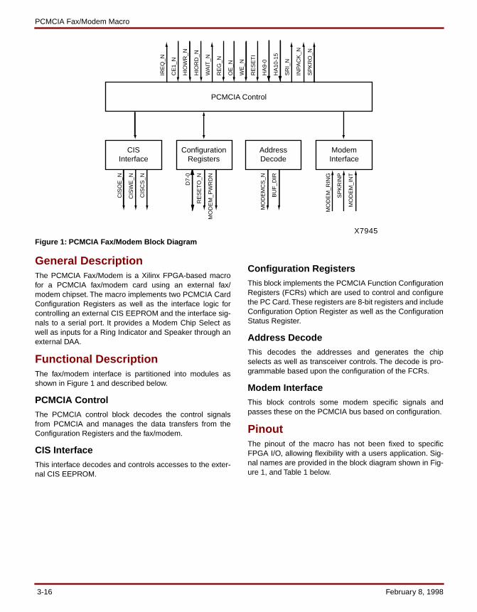
PCMCIA Fax/Modem Macro
ConfigurationRegisters
AddressDecode
ModemInterface
D7-
0
RE
SE
TO
_N
MO
DE
M_P
WR
DN
MO
DE
MC
S_N
BU
F_D
IR
MO
DE
M_R
ING
SP
KR
INP
MO
DE
M_I
NT
CIS
OE
_N
CIS
WE
_N
CIS
CS
_N
CISInterface
IRE
Q_N
CE
1_N
HIO
WR
_N
HIO
RD
_N
WA
IT_N
RE
G_N
OE
_N
WE
_N
RE
SE
TI
HA
9-0
HA
10-1
5
SR
I_N
INP
AC
K_N
SP
KR
O_N
PCMCIA Control
X7945
General DescriptionThe PCMCIA Fax/Modem is a Xilinx FPGA-based macrofor a PCMCIA fax/modem card using an external fax/modem chipset. The macro implements two PCMCIA CardConfiguration Registers as well as the interface logic forcontrolling an external CIS EEPROM and the interface sig-nals to a serial port. It provides a Modem Chip Select aswell as inputs for a Ring Indicator and Speaker through anexternal DAA.
Functional DescriptionThe fax/modem interface is partitioned into modules asshown in Figure 1 and described below.
PCMCIA ControlThe PCMCIA control block decodes the control signalsfrom PCMCIA and manages the data transfers from theConfiguration Registers and the fax/modem.
CIS InterfaceThis interface decodes and controls accesses to the exter-nal CIS EEPROM.
Configuration RegistersThis block implements the PCMCIA Function ConfigurationRegisters (FCRs) which are used to control and configurethe PC Card. These registers are 8-bit registers and includeConfiguration Option Register as well as the ConfigurationStatus Register.
Address DecodeThis decodes the addresses and generates the chipselects as well as transceiver controls. The decode is pro-grammable based upon the configuration of the FCRs.
Modem InterfaceThis block controls some modem specific signals andpasses these on the PCMCIA bus based on configuration.
PinoutThe pinout of the macro has not been fixed to specificFPGA I/O, allowing flexibility with a users application. Sig-nal names are provided in the block diagram shown in Fig-ure 1, and Table 1 below.
Figure 1: PCMCIA Fax/Modem Block Diagram
3-16 February 8, 1998
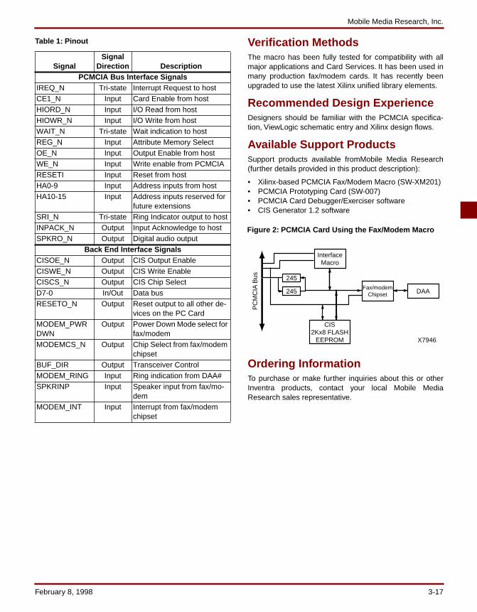
Mobile Media Research, Inc.
Table 1: Pinout Verification MethodsThe macro has been fully tested for compatibility with allmajor applications and Card Services. It has been used inmany production fax/modem cards. It has recently beenupgraded to use the latest Xilinx unified library elements.
Recommended Design ExperienceDesigners should be familiar with the PCMCIA specifica-tion, ViewLogic schematic entry and Xilinx design flows.
Available Support ProductsSupport products available fromMobile Media Research(further details provided in this product description):
• Xilinx-based PCMCIA Fax/Modem Macro (SW-XM201)• PCMCIA Prototyping Card (SW-007)• PCMCIA Card Debugger/Exerciser software• CIS Generator 1.2 software
Ordering InformationTo purchase or make further inquiries about this or otherInventra products, contact your local Mobile MediaResearch sales representative.
SignalSignal
Direction DescriptionPCMCIA Bus Interface Signals
IREQ_N Tri-state Interrupt Request to hostCE1_N Input Card Enable from hostHIORD_N Input I/O Read from hostHIOWR_N Input I/O Write from hostWAIT_N Tri-state Wait indication to hostREG_N Input Attribute Memory SelectOE_N Input Output Enable from hostWE_N Input Write enable from PCMCIARESETI Input Reset from hostHA0-9 Input Address inputs from hostHA10-15 Input Address inputs reserved for
future extensionsSRI_N Tri-state Ring Indicator output to hostINPACK_N Output Input Acknowledge to hostSPKRO_N Output Digital audio output
Back End Interface SignalsCISOE_N Output CIS Output EnableCISWE_N Output CIS Write EnableCISCS_N Output CIS Chip SelectD7-0 In/Out Data busRESETO_N Output Reset output to all other de-
vices on the PC CardMODEM_PWRDWN
Output Power Down Mode select for fax/modem
MODEMCS_N Output Chip Select from fax/modem chipset
BUF_DIR Output Transceiver ControlMODEM_RING Input Ring indication from DAA#SPKRINP Input Speaker input from fax/mo-
demMODEM_INT Input Interrupt from fax/modem
chipset
Figure 2: PCMCIA Card Using the Fax/Modem Macro
CIS2Kx8 FLASH
EEPROM
InterfaceMacro
DAAFax/modem
Chipset
PC
MC
IA B
us 245
245
X7946
February 8, 1998 3-17
PCMCIA Fax/Modem Macro
Related Information
Personal Computer Memory Card International AssociationThe PCMCIA publishes PC-Card specifications and relateddocuments. For information contact:
PCMCIA Headquarters2635 North First Street, Suite 209San Jose, CA 95134 USAPhone: +1 408-433-CARD (2273)Fax: +1 408-433-9558E-mail: [email protected]: www.pc-card.com
Xilinx Programmable LogicFor information on Xilinx programmable logic or develop-ment system software, contact your local Xilinx sales office,or:
Xilinx, Inc.2100 Logic DriveSan Jose, CA 95124Phone: +1 408-559-7778Fax: +1 408-559-7114URL: www.xilinx.com
For general Xilinx literature, contact:
Phone: +1 800-231-3386 (inside the US)+1 408-879-5017 (outside the US)
E-mail: [email protected]
For AllianceCORETM specific information, contact:
Phone: +1 408-879-5381E-mail: [email protected]: www.xilinx.com/products/logicore/alliance/
tblpart.htm
3-18 February 8, 1998
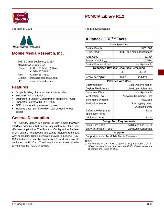
PCMCIA Library R1.2
February 8, 1998 Product Specification
Mobile Media Research, Inc.
39675 Cedar Boulevard, #295ANewark,CA 94560 USAPhone: 1-800-799-MMRI (6674)
+1 510-657-4891Fax: +1 510-657-4892E-mail: [email protected]: www.mobmedres.com
Features• Simple building blocks for user customization• Built-in PCMCIA Interface• Support for Function Configuration Registers (FCR)• Support for external CIS EEPROM• FCR bit decode implemented by user• Includes a test primitive which can be used to test
socket
General DescriptionThe PCMCIA Library is a library of very simple PCMCIAinterface primitives that can be fully customized for a spe-cific user application. The Function Configuration Register(FCR) bits are not decoded and can be implemented in anyway necessary. These primitives provide a generic PCM-CIA interface and can be customized to work with any I/Odevice on the PC Card. The library includes a test primitiveto help test the PCMCIA socket.
.
Notes:1. IOB count is for CIS, PCMCG1 (both 33 I/O) and PCMCG1 (32 I/O) primitives only; test primitive uses 58 I/O; I/O counts assume
all signals are routed off-chip.
AllianceCORE TM FactsCore Specifics
Device Family XC3x00ACLBs Used 20-30, see block descriptions
IOBs Used 32/331
System Clock fmax 10 MHzDevice Features Used Not Applicable
Supported Devices/Resources Remaining
I/O CLBs
XC3x42A TQ100 50/492 114-124Provided with Core
Documentation User DocumentationDesign File Formats ViewLogic SchematicConstraint Files Not ApplicableVerification Tool ViewSim Command FilesSchematic Symbols ViewlogicEvaluation Model Prototyping board
Available extraReference designs & application notes
None
Additional Items NoneDesign Tool Requirements
Xilinx Core Tools XACTstep 5.2.1/6.0.1Entry/Verification Tools ViewLogic Schematic
SupportSupport provided by Mobile Media Research
February 8, 1998 3-19
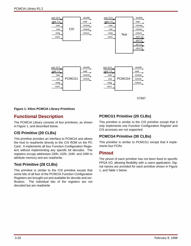
PCMCIA Library R1.2
sad 15-0
sdat 7-0
xwe
xoe
xreg
xce1
xbufdir
wait
romwe
romoe
romcs
PCMCG4
sad 15-0
sdat 7-0
xwe
xoe
xreg
xce1
xbufdir
wait
romwe
romoePCMCG1
sad 15-0
sdat 7-0
xwe
xoe
xreg
xce1
xbufdir
wait
romwe
romoe
romcs
CIS
sad 15-0
sdat 7-0
xwe
xoe
xreg
xce1
xbufdir
wait
romwe
romoe
romcs
xta7-12
xtb7-0
xtc7-0
xdc2-0
Test
X7947
Functional DescriptionThe PCMCIA Library consists of four primitives, as shownin Figure 1, and described below.
CIS Primitive (20 CLBs)This primitive provides an interface to PCMCIA and allowsthe host to read/write directly to the CIS ROM on the PCCard. It implements all four Function Configuration Regis-ters without implementing any specific bit decodes. Theregisters occupy addresses 100h, 102h, 104h and 106h inattribute memory and are read/write.
Test Primitive (28 CLBs)This primitive is similar to the CIS primitive except thatsome bits of all four of the PCMCIA Function ConfigurationRegisters are brought out and available for decode and ver-ification. The individual bits of the registers are notdecoded but are read/write
PCMCG1 Primitive (20 CLBs)This primitive is similar to the CIS primitive except that itonly implements one Function Configuration Register andCIS accesses are not supported.
PCMCG4 Primitive (30 CLBs)This primitive is similar to PCMCG1 except that it imple-ments four FCRs
PinoutThe pinout of each primitive has not been fixed to specificFPGA I/O, allowing flexibility with a users application. Sig-nal names are provided for each primitive shown in Figure1, and Table 1 below.
Figure 1: Xilinx PCMCIA Library Primitives
3-20 February 8, 1998
Mobile Media Research, Inc.
Verification MethodsThe primitives have been fully tested for compatibility withall major applications and Card Services. They haverecently been upgraded to use the latest Xilinx unifiedlibrary elements.
Recommended Design ExperienceDesigners should be familiar with the PCMCIA specifica-tion, ViewLogic schematic entry and Xilinx design flows.
Available Support ProductsSupport products available fromMobile Media Research:
• PCMCIA Prototyping Card• PCMCIA Card Debugger/Exerciser software• CIS Generator 1.2 software
Ordering InformationTo purchase or make further inquiries about this or otherMobile Media Research products, contact MMR directly.
Related Information
Personal Computer Memory Card International AssociationThe PCMCIA publishes PC-Card specifications and relateddocuments. For information, contact:
PCMCIA Headquarters2635 North First Street, Suite 209San Jose, CA 95134 USAPhone: +1 408-433-CARD (2273)Fax: +1 408-433-9558E-mail: [email protected]: www.pc-card.com
Xilinx Programmable LogicFor information on Xilinx programmable logic or develop-ment system software, contact your local Xilinx sales office,or:
Xilinx, Inc.2100 Logic DriveSan Jose, CA 95124Phone: +1 408-559-7778Fax: +1 408-559-7114URL: www.xilinx.com
For general Xilinx literature, contact:
Phone: +1 800-231-3386 (inside the US)+1 408-879-5017 (outside the US)
E-mail: [email protected]
For AllianceCORETM specific information, contact:
Phone: +1 408-879-5381E-mail: [email protected]: www.xilinx.com/products/logicore/alliance/ tblpart.htm
Table 1: PCMCIA Library Primitives Signal Pinout
SignalSignal
Direction DescriptionCommon Signals for all Primitivessad 15-0 Input Host addresssdat 7-0 In/Out Host dataxwe Input Write Enablexoe Input Output Enablexreg Input Attribute Memory Select
from hostxce1 Input Card Enable from hostxbufdir Output Controls direction of data
bufferwait Output Inserts delay in completion of
cycle to the hostromwe Output Write enable to CIS EE-
PROMromoe Output Output Enable to CIS EE-
PROMAdditional Signals for CIS and PCMCG4 Primitives
romcs Output Chip Select to CIS EEPROM
Additional Signals for Test Primitiveromcs Output Chip Select to CIS EEPROMxta 7-2 Output FCR 0 bits 7-2xtb 7-1 Output FCR 1 bits 7-1xtc 7-0 Output FCR 2 bits 7-0xdc 2-0 Output FCR 3 bits 2 -0
February 8, 1998 3-21
PCMCIA Library R1.2
3-22 February 8, 1998
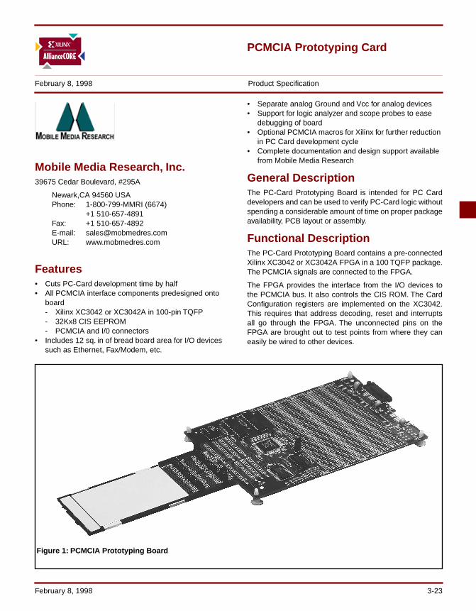
PCMCIA Prototyping Card
February 8, 1998 Product Specification
Mobile Media Research, Inc. 39675 Cedar Boulevard, #295A
Newark,CA 94560 USAPhone: 1-800-799-MMRI (6674)
+1 510-657-4891Fax: +1 510-657-4892E-mail: [email protected]: www.mobmedres.com
Features• Cuts PC-Card development time by half• All PCMCIA interface components predesigned onto
board- Xilinx XC3042 or XC3042A in 100-pin TQFP- 32Kx8 CIS EEPROM- PCMCIA and I/0 connectors
• Includes 12 sq. in of bread board area for I/O devices such as Ethernet, Fax/Modem, etc.
• Separate analog Ground and Vcc for analog devices• Support for logic analyzer and scope probes to ease
debugging of board• Optional PCMCIA macros for Xilinx for further reduction
in PC Card development cycle• Complete documentation and design support available
from Mobile Media Research
General DescriptionThe PC-Card Prototyping Board is intended for PC Carddevelopers and can be used to verify PC-Card logic withoutspending a considerable amount of time on proper packageavailability, PCB layout or assembly.
Functional DescriptionThe PC-Card Prototyping Board contains a pre-connectedXilinx XC3042 or XC3042A FPGA in a 100 TQFP package.The PCMCIA signals are connected to the FPGA.
The FPGA provides the interface from the I/O devices tothe PCMCIA bus. It also controls the CIS ROM. The CardConfiguration registers are implemented on the XC3042.This requires that address decoding, reset and interruptsall go through the FPGA. The unconnected pins on theFPGA are brought out to test points from where they caneasily be wired to other devices.
Figure 1: PCMCIA Prototyping Board
February 8, 1998 3-23
PCMCIA Prototyping Card
The FPGA can be configured either from the XC1736PROM or from a host via a download cable. The jumper J1allows the user to select the programming option.
A 12 square-inch breadboard area is provided for I/Odevices. Up to four memory or I/O devices can be put ontothe bread-board area. Power and ground strips are pro-vided throughout to support additional devices. Separateanalog Ground and Vcc are provided for I/O devices requir-ing analog signals.
Also included on the board is a logic analyzer strip to assistin tracing hardware or software problems. All PCMCIA sig-nals are routed to the logic analyzer strip. Other signals(from the FPGA, CIS or I/O) can easily be accessed eitherthrough test points or in the breadboard area.
DocumentationThe following documentation is provided with the PC-CardPrototyping Card:
• Board schematic• Board specifications• Application brief on developing PC-Cards• Sample modem card CIS• A list of soft macros for the Xilinx device available from
Mobile Media Research.
Available Support ProductsMobile Media Research supplies a complete line of PCM-CIA design products. Contact DO for additional information.
• PCMCIA Fax/Modem Macro• PCMCIA Library V1.2• CIS Generator 1.2 software
Ordering InformationThis product is available from the AllianceCORETM partnerlisted on the first page. Please contact the partner for pric-ing and more information.
Related InformationFor information on Xilinx programmable logic or develop-ment system software, contact your local Xilinx sales office,or:
Xilinx, Inc.2100 Logic DriveSan Jose, CA 95124Phone: +1 408-559-7778Fax: +1 408-559-7114URL: www.xilinx.com
For general Xilinx literature, contact:
Phone: +1 800-231-3386 (inside the US)+1 408-879-5017 (outside the US)
E-mail: [email protected]
For AllianceCORETM specific information, contact:
Phone: +1 408-879-5381E-mail: [email protected]: www.xilinx.com/products/logicore/alliance/
tblpart.htm
3-24 February 8, 1998
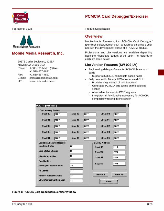
PCMCIA Card Debugger/Exerciser
February 8, 1998 Product Specification
Mobile Media Research, Inc.
39675 Cedar Boulevard, #295ANewark,CA 94560 USAPhone: 1-800-799-MMRI (6674)
+1 510-657-4891Fax: +1 510-657-4892E-mail: [email protected]: www.mobmedres.com
OverviewMobile Media Research, Inc. PCMCIA Card Debugger/Exerciser is designed for both hardware and software engi-neers in the development phase of a PCMCIA product.
Professional and Lite versions are available dependingupon the needs and budget of the user. The features ofeach are listed below.
Lite Version Features (SW-002-LV)• Engineering debug software for PCMCIA hosts and
cards- Supports 82365SL-compatible based hosts
• Fully compatible Microsoft Windows-based GUI- Provides easy control of host functions- Generates PCMCIA bus cycles on the selected
socket- Allows direct access to PCIC registers- Integrates all functionality necessary for PCMCIA
compatibility testing in one screen
Figure 1: PCMCIA Card Debugger/Exerciser Window
February 8, 1998 3-25
PCMCIA Card Debugger/Exerciser
• Supports basic and necessary PCMCIA debug and testing features:- Register access- I/O and memory window set-up- Socket configuration access
Professional Version Features (SW-002-PV)• All features of Lite version plus these debug and test
features:- Card Configuration Register support, up to 16
registers, especially useful for multi-function cards- ATA card debug module (supports ATA interface)- Built-in CIS Parcel, with tuple browser to read the
CIS• Built-in command Macro/Interpreter
- Supports user programmable “Macro” commands to generate system cycles for PCMCIA host/card debug
- Up to eight user-defined command lines- Trace, Normal and Step options- Loop control capability- Results displayed in monitor window
• Excellent for high-volume testing• Ideal for Host or PC-Card debug, characterization and
evaluation
Available Support ProductsSupport products available from Mobile Media Research,Inc. (further details provided in this product description)
• PCMCIA Prototyping Card• CIS Generator 1.2 software
Ordering InformationTo purchase or make further inquiries about this or otherMMRI products, contact Mobile Media Research, Inc.directly.
Related Information
Xilinx Programmable LogicFor information on Xilinx programmable logic or develop-ment system software, contact your local Xilinx sales office,or:
Xilinx, Inc.2100 Logic DriveSan Jose, CA 95124Phone: +1 408-559-7778Fax: +1 408-559-7114URL: www.xilinx.com
For general Xilinx literature, contact:
Phone: +1 800-231-3386 (inside the US)+1 408-879-5017 (outside the US)
E-mail: [email protected]
For AllianceCORETM specific information, contact:
Phone: +1 408-879-5381E-mail: [email protected]: www.xilinx.com/products/logicore/alliance/
tblpart.htm
3-26 February 8, 1998
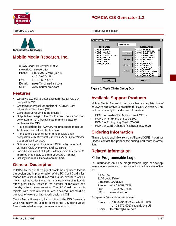
PCMCIA CIS Generator 1.2
February 8, 1998 Product Specification
Mobile Media Research, Inc.
39675 Cedar Boulevard, #295ANewark,CA 94560 USAPhone: 1-800-799-MMRI (6674)
+1 510-657-4891Fax: +1 510-657-4892E-mail: [email protected]: www.mobmedres.com
Features• Windows 3.1 tool to enter and generate a PCMCIA
compatible CIS• Graphical entry tool for design of PCMCIA Card
Information Structures (CIS)• Generates Level One Tuple chains• Outputs Hex image of the CIS to a file. The file can then
be written to PC-Card attribute memory space to implement the CIS
• Provides options for PCMCIA recommended minimum Tuples or user defined Tuple chain
• Provides the option of generating a Tuple chain compatible with Microsoft Windows 95 or SystemSoft’s CardSoft card services
• Option for support of minimum CIS configurations of various PCMCIA memory and I/O cards
• Form-based layout of Tuples, allows users to enter CIS information logically and in a structured manner
• Greatly reduces CIS development time
General DescriptionIn PCMCIA, one of the biggest problems engineers face isthe design and implementation of the PC-Card Card Infor-mation Structure (CIS). It is a tedious job, similar to writingCPU machine code. Doing this manually can significantlyaffect productivity, increase the number of mistakes andthereby affect time-to-market. The PC-Card market isreplete with products which are declared incompatiblebecause of wrong or improperly designed CIS.
Mobile Media Research, Inc. solution is the CIS Generatorwhich will allow the user to compile the CIS using visualforms instead of error-prone manual methods.
Available Support ProductsMobile Media Research, Inc. supplies a complete line ofhardware and software products for PCMCIA design. Con-tact them directly for additional information.
• PCMCIA Fax/Modem Macro (SW-XM201)• PCMCIA library R1.2 (SW-XL200)• PCMCIA Prototyping Card (SW-007)• PCMCIA Card Debugger/Exerciser (SW-002)
Ordering InformationThis product is available from the AllianceCORETM partner.Please contact the partner for pricing and more informa-tion.
Related Information
Xilinx Programmable LogicFor information on Xilinx programmable logic or develop-ment system software, contact your local Xilinx sales office,or:
Xilinx, Inc.2100 Logic DriveSan Jose, CA 95124Phone: +1 408-559-7778Fax: +1 408-559-7114URL: www.xilinx.com
For general Xilinx literature, contact:
Phone: +1 800-231-3386 (inside the US)+1 408-879-5017 (outside the US)
E-mail: [email protected]
Figure 1: Tuple Chain Dialog Box
February 8, 1998 3-27
PCMCIA CIS Generator 1.2
For AllianceCORETM specific information, contact:
Phone: +1 408-879-5381E-mail: [email protected]
URL: www.xilinx.com/products/logicore/alliance/tblpart.htm
3-28 February 8, 1998
Low-Speed USB Function Controller
February 8, 1998 Product Specification
Inventra A Business Unit of Mentor Graphics1001 Ridder Park DriveSan Jose, CA 95134-2314 USAURL: www.mentorg.com/inventra
Features• Fully compliant to USB 1.0 specification• 100% programmable single-chip solution with
customizable back-end functionality• Pre-defined implementation for predictable timing in
Xilinx FPGA or HardWireTM - Push button scripts to place and route, and generate
Xilinx bit files- Xilinx-optimized place and route constraint and
guide files• Fully verified design
- Simulated using Inventra USB Simulation Model- Hardware-proven in a Xilinx FPGA at USB-IF
sponsored interoperability workshop- Complete synchronous design
• Provides a high level interface that shields the firmware from USB protocol details
• Complete device configuration• Compatible with both OpenHCI and Intel UHCI
standards• Supports low-speed (1.5 Mbps) functions• Endpoint 0 is Control endpoint
- Maximum packet capacity is 8 Bytes• IN Endpoint for Interrupt data transfers
- Maximum packet capacity for In Endpoint is user selectable from 1-8 Bytes
• Automatic Data Retry, Error recovery, and Data Toggle synchronization performed in hardware
• Includes the following error handling capabilities- CRC errors- Response Time Out
• ID error• External interface to Phillips IPDIUSBP11 USB
transceiver
Notes:
1. Assuming all core signals are routed off-chip.2. For 10-15% of design, remaining logic operates at 1/4
max clock.
AllianceCORE TM FactsCore Specifics
Device Family XC4000ECLBs Used 600
IOBs Used 291
System Clock fmax 6MHz2
Device Features Used
RAM, 3-state buses, carry logic
Supported Devices/Resources RemainingI/O CLBs
XC4025E-4 HQ240 1641 304
Provided with CoreDocumentation XC4000E/CX5215 Datasheets
Core documentationSample files for top level module in
Verilog HDLDesign File Formats XNF Netlist
Verilog Source RTL AvailableConstraint Files Timespec, .cst, .tnm filesVerification Tool VerilogSchematic Symbols Viewlogic, ORCADEvaluation Model Evaluation Board
available extraReference designs & application notes
None
Additional Items Firmware for microcontroller avail-able for nominal cost
Design Tool RequirementsXilinx Core Tools XACTstep 5.2.1/6.0.1Entry/Verification Verilog RTL
SupportSupport provided by Inventra
February 8, 1998 3-29
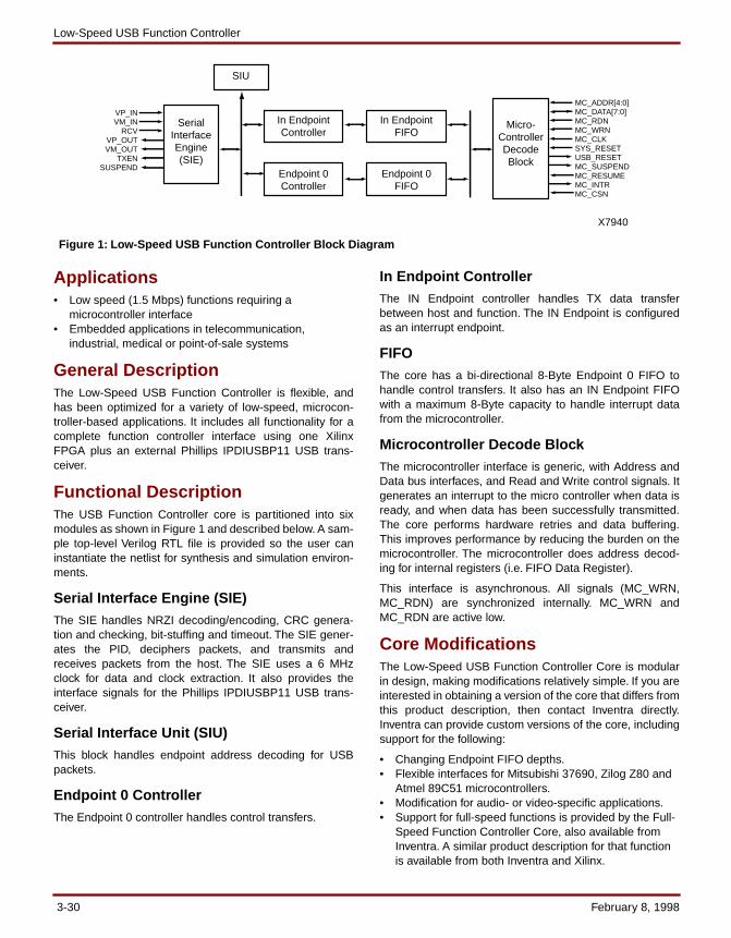
Low-Speed USB Function Controller
Applications• Low speed (1.5 Mbps) functions requiring a
microcontroller interface• Embedded applications in telecommunication,
industrial, medical or point-of-sale systems
General DescriptionThe Low-Speed USB Function Controller is flexible, andhas been optimized for a variety of low-speed, microcon-troller-based applications. It includes all functionality for acomplete function controller interface using one XilinxFPGA plus an external Phillips IPDIUSBP11 USB trans-ceiver.
Functional DescriptionThe USB Function Controller core is partitioned into sixmodules as shown in Figure 1 and described below. A sam-ple top-level Verilog RTL file is provided so the user caninstantiate the netlist for synthesis and simulation environ-ments.
Serial Interface Engine (SIE)The SIE handles NRZI decoding/encoding, CRC genera-tion and checking, bit-stuffing and timeout. The SIE gener-ates the PID, deciphers packets, and transmits andreceives packets from the host. The SIE uses a 6 MHzclock for data and clock extraction. It also provides theinterface signals for the Phillips IPDIUSBP11 USB trans-ceiver.
Serial Interface Unit (SIU)This block handles endpoint address decoding for USBpackets.
Endpoint 0 ControllerThe Endpoint 0 controller handles control transfers.
In Endpoint ControllerThe IN Endpoint controller handles TX data transferbetween host and function. The IN Endpoint is configuredas an interrupt endpoint.
FIFOThe core has a bi-directional 8-Byte Endpoint 0 FIFO tohandle control transfers. It also has an IN Endpoint FIFOwith a maximum 8-Byte capacity to handle interrupt datafrom the microcontroller.
Microcontroller Decode BlockThe microcontroller interface is generic, with Address andData bus interfaces, and Read and Write control signals. Itgenerates an interrupt to the micro controller when data isready, and when data has been successfully transmitted.The core performs hardware retries and data buffering.This improves performance by reducing the burden on themicrocontroller. The microcontroller does address decod-ing for internal registers (i.e. FIFO Data Register).
This interface is asynchronous. All signals (MC_WRN,MC_RDN) are synchronized internally. MC_WRN andMC_RDN are active low.
Core ModificationsThe Low-Speed USB Function Controller Core is modularin design, making modifications relatively simple. If you areinterested in obtaining a version of the core that differs fromthis product description, then contact Inventra directly.Inventra can provide custom versions of the core, includingsupport for the following:
• Changing Endpoint FIFO depths.• Flexible interfaces for Mitsubishi 37690, Zilog Z80 and
Atmel 89C51 microcontrollers.• Modification for audio- or video-specific applications.• Support for full-speed functions is provided by the Full-
Speed Function Controller Core, also available from Inventra. A similar product description for that function is available from both Inventra and Xilinx.
Figure 1: Low-Speed USB Function Controller Block Diagram
SIU
In EndpointFIFO
Endpoint 0FIFO
In EndpointController
Endpoint 0Controller
VP_INVM_IN
RCVVP_OUTVM_OUT
TXENSUSPEND
SerialInterfaceEngine(SIE)
MC_ADDR[4:0]MC_DATA[7:0]MC_RDNMC_WRNMC_CLKSYS_RESETUSB_RESETMC_SUSPENDMC_RESUMEMC_INTRMC_CSN
Micro-ControllerDecodeBlock
X7940
3-30 February 8, 1998
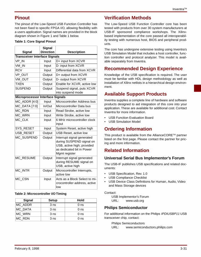
InventraTM
Pinout The pinout of the Low-Speed USB Function Controller hasnot been fixed to specific FPGA I/O, allowing flexibility witha users application. Signal names are provided in the blockdiagram shown in Figure 1 and Table 1 below.
Table 1: Core Signal Pinout
Table 2: Microcontroller I/O Timing
Verification MethodsThe Low-Speed USB Function Controller core has beentested with products from over 30 system manufacturers atUSB-IF sponsored compliance workshops. The Xilinx-based implementation of the core passed all interoperabil-ity testing with numerous host, BIOS and peripheral prod-ucts.
The core has undergone extensive testing using Inventra’sUSB Simulation Model that includes a host controller, func-tion controller and protocol analyzer. This model is avail-able separately from Inventra.
Recommended Design ExperienceKnowledge of the USB specification is required. The usermust be familiar with HDL design methodology as well asinstallation of Xilinx netlists in a hierarchical design environ-ment.
Available Support ProductsInventra supplies a complete line of hardware and softwareproducts designed to aid integration of this core into yourapplication. These are available for additional cost. ContactInventra for more information.
• USB Function Evaluation Board • USB Simulation Model
Ordering InformationThis product is available from the AllianceCORETM partnerlisted on the first page. Please contact the partner for pric-ing and more information.
Related Information
Universal Serial Bus Implementor’s ForumThe USB-IF publishes USB specifications and related doc-uments:
• USB Specification, Rev. 1.0• USB Compliance Checklist• USB Device Class Definitions for Human, Audio, Video
and Mass Storage devices
Contact:USB Implementor’s ForumURL: www.usb.org
Philips SemiconductorFor additional information on the Philips IPDIUSBP11 USBtransceiver chip, contact:
Philips SemiconductorsURL: www.semiconductors.philips.com
SignalSignal
Direction DescriptionTransceiver Interface SignalsVP_IN Input D+ input from XCVRVM_IN Input D- input from XCVRRCV Input Differential data from XCVRVP_OUT Output D+ output from XCVRVM_OUT Output D- output from XCVRTXEN Output Enable for XCVR, active lowSUSPEND Output Suspend signal, puts XCVR
into suspend modeMicroprocessor Interface SignalsMC_ADDR [4:0] Input Microcontroller Address busMC_DATA [7:0] In/Out Microcontroller Data busMC_RDN Input Read Strobe, active lowMC_WRN Input Write Strobe, active lowMC_CLK Input 6 MHz microcontroller clock
inputSYS_RESET Input System Reset, active highUSB_RESET Output USB Reset, active lowMC_SUSPEND Output Interrupt signal generated
during SUSPEND signal on USB, active high; provided as dedicated bit in Power Mgmt register
MC_RESUME Output Interrupt signal generated during RESUME signal on USB, active high
MC_INTR Output Microcontroller Interrupts, active low
MC_CSN Input Acts as a Block Select to mi-crocontroller address, active low
Signal Setup HoldMC_ADDR 3 ns 0 nsMC_DATA 3 ns 0 nsMC_WRN 3 ns 0 nsMC_RDN 3 ns 0 ns
February 8, 1998 3-31
Low-Speed USB Function Controller
Xilinx Programmable LogicFor information on Xilinx programmable logic or develop-ment system software, contact your local Xilinx sales office,or:
Xilinx, Inc.2100 Logic DriveSan Jose, CA 95124Phone: +1 408-559-7778Fax: +1 408-559-7114URL: www.xilinx.com
For general Xilinx literature, contact:
Phone: +1 800-231-3386 (inside the US)+1 408-879-5017 (outside the US)
E-mail: [email protected]
For AllianceCORETM specific information, contact:
Phone: +1 408-879-5381E-mail: [email protected]: www.xilinx.com/products/logicore/alliance/
tblpart.htm
3-32 February 8, 1998
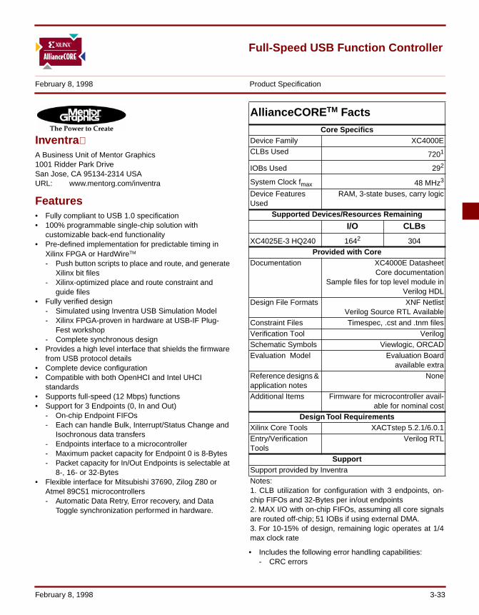
Full-Speed USB Function Controller
February 8, 1998 Product Specification
Inventra A Business Unit of Mentor Graphics1001 Ridder Park DriveSan Jose, CA 95134-2314 USAURL: www.mentorg.com/inventra
Features• Fully compliant to USB 1.0 specification• 100% programmable single-chip solution with
customizable back-end functionality• Pre-defined implementation for predictable timing in
Xilinx FPGA or HardWireTM - Push button scripts to place and route, and generate
Xilinx bit files- Xilinx-optimized place and route constraint and
guide files• Fully verified design
- Simulated using Inventra USB Simulation Model- Xilinx FPGA-proven in hardware at USB-IF Plug-
Fest workshop- Complete synchronous design
• Provides a high level interface that shields the firmware from USB protocol details
• Complete device configuration• Compatible with both OpenHCI and Intel UHCI
standards• Supports full-speed (12 Mbps) functions• Support for 3 Endpoints (0, In and Out)
- On-chip Endpoint FIFOs- Each can handle Bulk, Interrupt/Status Change and
Isochronous data transfers- Endpoints interface to a microcontroller- Maximum packet capacity for Endpoint 0 is 8-Bytes- Packet capacity for In/Out Endpoints is selectable at
8-, 16- or 32-Bytes• Flexible interface for Mitsubishi 37690, Zilog Z80 or
Atmel 89C51 microcontrollers- Automatic Data Retry, Error recovery, and Data
Toggle synchronization performed in hardware.
• Includes the following error handling capabilities:- CRC errors
AllianceCORE TM FactsCore Specifics
Device Family XC4000ECLBs Used 7201
IOBs Used 292
System Clock fmax 48 MHz3
Device Features Used
RAM, 3-state buses, carry logic
Supported Devices/Resources Remaining
I/O CLBs
XC4025E-3 HQ240 1642 304Provided with Core
Documentation XC4000E DatasheetCore documentation
Sample files for top level module inVerilog HDL
Design File Formats XNF NetlistVerilog Source RTL Available
Constraint Files Timespec, .cst and .tnm filesVerification Tool VerilogSchematic Symbols Viewlogic, ORCADEvaluation Model Evaluation Board
available extraReference designs & application notes
None
Additional Items Firmware for microcontroller avail-able for nominal cost
Design Tool RequirementsXilinx Core Tools XACTstep 5.2.1/6.0.1Entry/Verification Tools
Verilog RTL
SupportSupport provided by InventraNotes:1. CLB utilization for configuration with 3 endpoints, on-chip FIFOs and 32-Bytes per in/out endpoints2. MAX I/O with on-chip FIFOs, assuming all core signalsare routed off-chip; 51 IOBs if using external DMA.3. For 10-15% of design, remaining logic operates at 1/4max clock rate
February 8, 1998 3-33
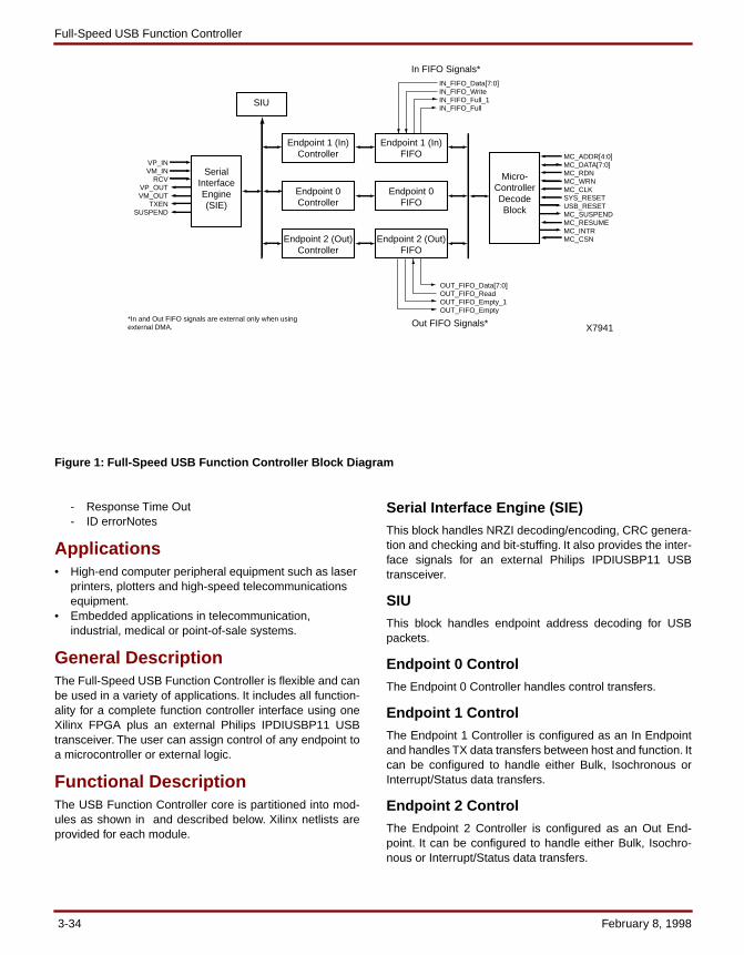
Full-Speed USB Function Controller
SIU
Endpoint 1 (In)FIFO
Endpoint 0FIFO
Endpoint 2 (Out)FIFO
Endpoint 1 (In)Controller
Endpoint 0Controller
Endpoint 2 (Out)Controller
VP_INVM_IN
RCVVP_OUTVM_OUT
TXENSUSPEND
SerialInterfaceEngine(SIE)
MC_ADDR[4:0]MC_DATA[7:0]MC_RDNMC_WRNMC_CLKSYS_RESETUSB_RESETMC_SUSPENDMC_RESUMEMC_INTRMC_CSN
Micro-ControllerDecodeBlock
IN_FIFO_Data[7:0]IN_FIFO_WriteIN_FIFO_Full_1IN_FIFO_Full
OUT_FIFO_Data[7:0]OUT_FIFO_ReadOUT_FIFO_Empty_1OUT_FIFO_Empty
In FIFO Signals*
Out FIFO Signals**In and Out FIFO signals are external only when usingexternal DMA. X7941
- Response Time Out- ID errorNotes
Applications• High-end computer peripheral equipment such as laser
printers, plotters and high-speed telecommunications equipment.
• Embedded applications in telecommunication, industrial, medical or point-of-sale systems.
General DescriptionThe Full-Speed USB Function Controller is flexible and canbe used in a variety of applications. It includes all function-ality for a complete function controller interface using oneXilinx FPGA plus an external Philips IPDIUSBP11 USBtransceiver. The user can assign control of any endpoint toa microcontroller or external logic.
Functional DescriptionThe USB Function Controller core is partitioned into mod-ules as shown in and described below. Xilinx netlists areprovided for each module.
Serial Interface Engine (SIE)This block handles NRZI decoding/encoding, CRC genera-tion and checking and bit-stuffing. It also provides the inter-face signals for an external Philips IPDIUSBP11 USBtransceiver.
SIUThis block handles endpoint address decoding for USBpackets.
Endpoint 0 ControlThe Endpoint 0 Controller handles control transfers.
Endpoint 1 ControlThe Endpoint 1 Controller is configured as an In Endpointand handles TX data transfers between host and function. Itcan be configured to handle either Bulk, Isochronous orInterrupt/Status data transfers.
Endpoint 2 ControlThe Endpoint 2 Controller is configured as an Out End-point. It can be configured to handle either Bulk, Isochro-nous or Interrupt/Status data transfers.
Figure 1: Full-Speed USB Function Controller Block Diagram
3-34 February 8, 1998
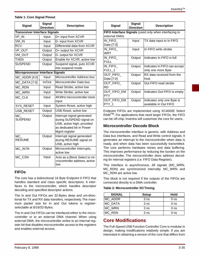
InventraTM
Table 1: Core Signal Pinout
FIFOsThe core has a bidirectional 16 Byte Endpoint 0 FIFO thathandles standard and class specific descriptors. It inter-faces to the microcontroller, which handles descriptordecoding and specified descriptor actions.
The In and Out FIFOs are 32-Bytes deep and uni-direc-tional for TX and RX data transfers, respectively. The maxi-mum packet size for In and Out tokens is register-selectable at 8/16/32-Bytes.
The In and Out FIFOs can be interfaced either to the micro-controller or to an external DMA channel. When usingexternal DMA, the microcontroller writes to an internal reg-ister bit that disables microcontroller access to the registersand enables external access.
Endpoint FIFOs are implemented using XC4000E SelectRAMTM. For applications that need larger FIFOs, the FIFOcan be off-chip. Inventra will customize the core for users.
Microcontroller Decode BlockThe microcontroller interface is generic, with Address andData bus interfaces, and Read and Write control signals. Itgenerates an interrupt to the microcontroller when data isready, and when data has been successfully transmitted.The core performs hardware retries and data buffering.This improves performance by reducing the burden on themicrocontroller. The microcontroller does address decod-ing for internal registers (i.e. FIFO Data Register).
This interface is asynchronous. All signals (MC_WRN,MC_RDN) are synchronized internally. MC_WRN andMC_RDN are active low.
This block is not required if the outputs of the FIFOs areconnected directly to a DMA controller.
Table 2: Microcontroller I/O Timing
Core ModificationsThe Full-Speed USB Function Controller Core is modular indesign, making modifications relatively simple. If you areinterested in obtaining a version of the core that differs from
SignalSignal
DirectionDescription
Transceiver Interface SignalsVP_IN Input D+ input from XCVRVM_IN Input D- input from XCVRRCV Input Differential data from XCVRVP_OUT Output D+ output for XCVRVM_OUT Output D- output for XCVRTXEN Output Enable for XCVR, active lowSUSPEND Output Suspend signal, puts XCVR
into suspend modeMicroprocessor Interface Signals
MC_ADDR [4:0] Input Microcontroller Address bus
MC_DATA [7:0] In/Out Microcontroller Data bus
MC_RDN Input Read Strobe, active low
MC_WRN Input Write Strobe, active low
MC_CLK Input 48 MHz microcontroller clock input
SYS_RESET Input System Reset, active high
USB_RESET Output USB Reset, active low
MC_SUSPEND
Output Interrupt signal generated during SUSPEND signal on USB, active high; provided as dedicated bit in Power Mgmt register
MC_RESUME
Output Interrupt signal generated during RESUME signal on USB, active high
MC_INTR Output Microcontroller Interrupts, active low
MC_CSN Input Acts as a Block Select to mi-crocontroller address, active low
SignalSignal
DirectionDescription
FIFO Interface Signals (used only when interfacing to external DMA)IN_FIFO_Data [7:0]
Input TX data input to In FIFO
IN_FIFO_WRT
Input In FIFO write strobe
IN_FIFO_FULL
Output Indicates In FIFO is full
IN_FIFO_FULL_1
Output Indicates In FIFO can accept only one more Byte
OUT_FIFO_Data [7:0]
Output RX data received from the host
OUT_FIFO_RD
Output Out FIFO read strobe
OUT_FIFO_EMPTY
Output Indicates Out FIFO is empty
OUT_FIFO_EMPTY_1
Output Indicates only one Byte is available in Out FIFO
SIGNAL Setup HoldMC_ADDR 3 ns 0 nsMC_DATA 3 ns 0 nsMC_WRN 3 ns 0 nsMC_RDN 3 ns 0 ns
February 8, 1998 3-35
Full-Speed USB Function Controller
this product description, then contact Inventra directly.Inventra can provide custom versions of the core, includingsupport for the following:
• Changing Endpoint FIFO depths.• Modification for audio- or video-specific applications.• Support for low-speed functions is provided by the Low-
Speed Function Controller Core, also available from Inventra. A similar product description for that function is available from both Inventra and Xilinx.
PinoutThe pinout of the Full-Speed USB Function Controller hasnot been fixed to specific FPGA I/O, allowing flexibility witha users application. Signal names are shown in the blockdiagram in Figure 1, and in Table 1.
Verification MethodsThe Full-Speed USB Function Controller core has beentested with products from over 30 system manufacturers atUSB-IF sponsored compliance workshops. The Xilinx-based implementation of the core passed all interoperabil-ity testing with numerous host, BIOS and peripheral prod-ucts.
The core has undergone extensive testing using InventraUSB Simulation Model that includes a host controller, func-tion controller and protocol analyzer. This model is avail-able separately from Inventra.
Recommended Design ExperienceKnowledge of the USB specification is required. The usermust be familiar with HDL design methodology as well asinstantiation of Xilinx netlists in a hierarchical design envi-ronment.
Available Support ProductsInventra supplies a complete line of hardware and softwareproducts designed to aid integration of this core into yourapplication. These are available for additional cost. ContactInventra for more information.
• USB Function Evaluation Board • USB Simulation Model
Ordering InformationThis product is available from the AllianceCORETM partnerlisted on the first page. Please contact the partner for pric-ing and more information.
Related Information
Universal Serial Bus Implementor’s ForumThe USB-IF publishes USB specifications and related doc-uments:
• USB Specification, Rev. 1.0• USB Compliance Checklist• USB Device Class Definitions for Human, Audio, Video
and Mass Storage devices
Contact:USB Implementor’s ForumURL: www.usb.org
Philips SemiconductorFor additional information on the Philips IPDIUSBP11 USBtransceiver chip, contact:
Philips SemiconductorsURL: www.semiconductors.philips.com
Xilinx Programmable LogicFor information on Xilinx programmable logic or develop-ment system software, contact your local Xilinx sales office,or:
Xilinx, Inc.2100 Logic DriveSan Jose, CA 95124Phone: +1 408-559-7778Fax: +1 408-559-7114URL: www.xilinx.com
For general Xilinx literature, contact:
Phone: +1 800-231-3386 (inside the US)+1 408-879-5017 (outside the US)
E-mail: [email protected]
For AllianceCORETM specific information, contact:
Phone: +1 408-879-5381E-mail: [email protected]: www.xilinx.com/products/logicore/alliance/
tblpart.htm
3-36 February 8, 1998
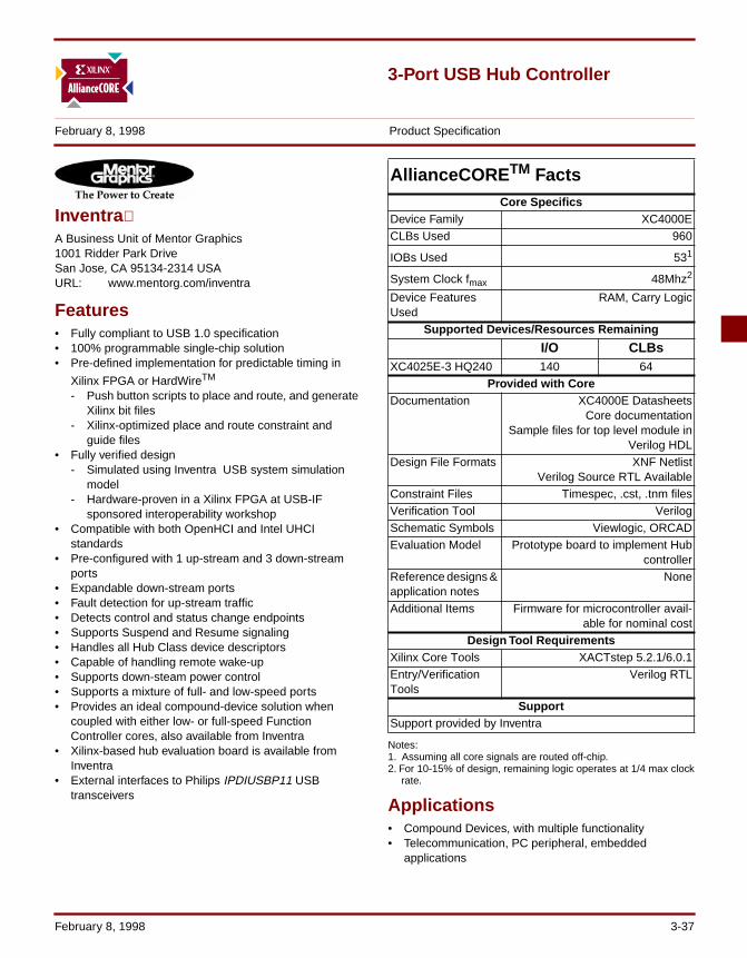
3-Port USB Hub Controller
February 8, 1998 Product Specification
Inventra A Business Unit of Mentor Graphics1001 Ridder Park DriveSan Jose, CA 95134-2314 USAURL: www.mentorg.com/inventra
Features• Fully compliant to USB 1.0 specification• 100% programmable single-chip solution• Pre-defined implementation for predictable timing in
Xilinx FPGA or HardWireTM - Push button scripts to place and route, and generate
Xilinx bit files- Xilinx-optimized place and route constraint and
guide files• Fully verified design
- Simulated using Inventra USB system simulation model
- Hardware-proven in a Xilinx FPGA at USB-IF sponsored interoperability workshop
• Compatible with both OpenHCI and Intel UHCI standards
• Pre-configured with 1 up-stream and 3 down-stream ports
• Expandable down-stream ports• Fault detection for up-stream traffic• Detects control and status change endpoints• Supports Suspend and Resume signaling• Handles all Hub Class device descriptors• Capable of handling remote wake-up• Supports down-steam power control• Supports a mixture of full- and low-speed ports• Provides an ideal compound-device solution when
coupled with either low- or full-speed Function Controller cores, also available from Inventra
• Xilinx-based hub evaluation board is available from Inventra
• External interfaces to Philips IPDIUSBP11 USB transceivers
Notes:1. Assuming all core signals are routed off-chip.2. For 10-15% of design, remaining logic operates at 1/4 max clock
rate.
Applications• Compound Devices, with multiple functionality• Telecommunication, PC peripheral, embedded
applications
AllianceCORE TM FactsCore Specifics
Device Family XC4000ECLBs Used 960
IOBs Used 531
System Clock fmax 48Mhz2
Device Features Used
RAM, Carry Logic
Supported Devices/Resources Remaining
I/O CLBsXC4025E-3 HQ240 140 64
Provided with CoreDocumentation XC4000E Datasheets
Core documentationSample files for top level module in
Verilog HDLDesign File Formats XNF Netlist
Verilog Source RTL AvailableConstraint Files Timespec, .cst, .tnm filesVerification Tool VerilogSchematic Symbols Viewlogic, ORCADEvaluation Model Prototype board to implement Hub
controllerReference designs & application notes
None
Additional Items Firmware for microcontroller avail-able for nominal cost
Design Tool RequirementsXilinx Core Tools XACTstep 5.2.1/6.0.1Entry/Verification Tools
Verilog RTL
SupportSupport provided by Inventra
February 8, 1998 3-37
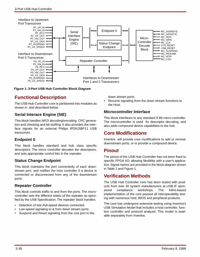
3-Port USB Hub Controller
Functional DescriptionThe USB Hub Controller core is partitioned into modules asshown in and described below.
Serial Interace Engine (SIE)This block handles NRZI decoding/encoding, CRC genera-tion and checking and bit-stuffing. It also provides the inter-face signals for an external Philips IPDIUSBP11 USBtransceiver.
Endpoint 0This block handles standard and hub class specificdescriptors. The micro controller decodes the descriptors,and sets appropriate control bits in the repeater.
Status Change EndpointThis block maintains the port connectivity of each down-stream port, and notifies the host controller if a device isconnected or disconnected from any of the downstreamports.
Repeater ControllerThis block controls traffic to and from the ports. The micro-controller sets the different states of the repeater as speci-fied by the USB Specification. The repeater block handles:
• Detection of low-/full-speed devices connected.• Low-speed signaling to & from down stream ports• Suspend and Reset signaling from the root port to the
down stream ports• Resume signaling from the down stream functions to
the Host.
Microcontroller InterfaceThis block interfaces to any standard 8 Bit micro controller.The microcontroller is used for descriptor decoding, andalso adds compound device capabilities to the hub.
Core ModificationsInventra will provide core modifications to add or removedownstream ports, or to provide a compound device.
PinoutThe pinout of the USB Hub Controller has not been fixed tospecific FPGA I/O, allowing flexibility with a user’s applica-tion. Signal names are provided in the block diagram shownin Table 1 and Figure 1.
Verification MethodsThe USB Hub Controller core has been tested with prod-ucts from over 30 system manufacturers at USB-IF spon-sored compliance workshops. The Xilinx-basedimplementation of the core passed all interoperability test-ing with numerous host, BIOS and peripheral products.
The core has undergone extensive testing using Inventra’sUSB Simulation Model that includes a host controller, func-tion controller and protocol analyzer. This model is avail-able separately from Inventra.
Endpoint 0
Status ChangeEndpoint
SerialInterfaceEngine(SIE)
Repeater Controller
Interface to UpstreamPort Transceiver
Interface to DownstreamPort 0 Transceiver
Interfaces to DownstreamPort 1 and 2 Transceivers
RT_VP_INRT_VM_IN
RT_RCVRT_VP_OUTRT_VM_OUTRT_UX_OEN
RT_SUSPENDRT_UX_SPEED
P0_VP_INP0_VM_IN
P0_RCVP0_VP_OUTP0_VM_OUTP0_UX_OEN
P0_SUSPENDP0_UX_SPEED
MC_ADDR[4:0]MC_DATA[7:0]MC_RDNMC_WRNMC_CLKSYS_RESETUSB_RESETMC_SUSPENDMC_RESUMEMC_INTRMC_CSN
Micro-ControllerDecodeBlock
Figure 1: 3-Port USB Hub Controller Block Diagram
3-38 February 8, 1998
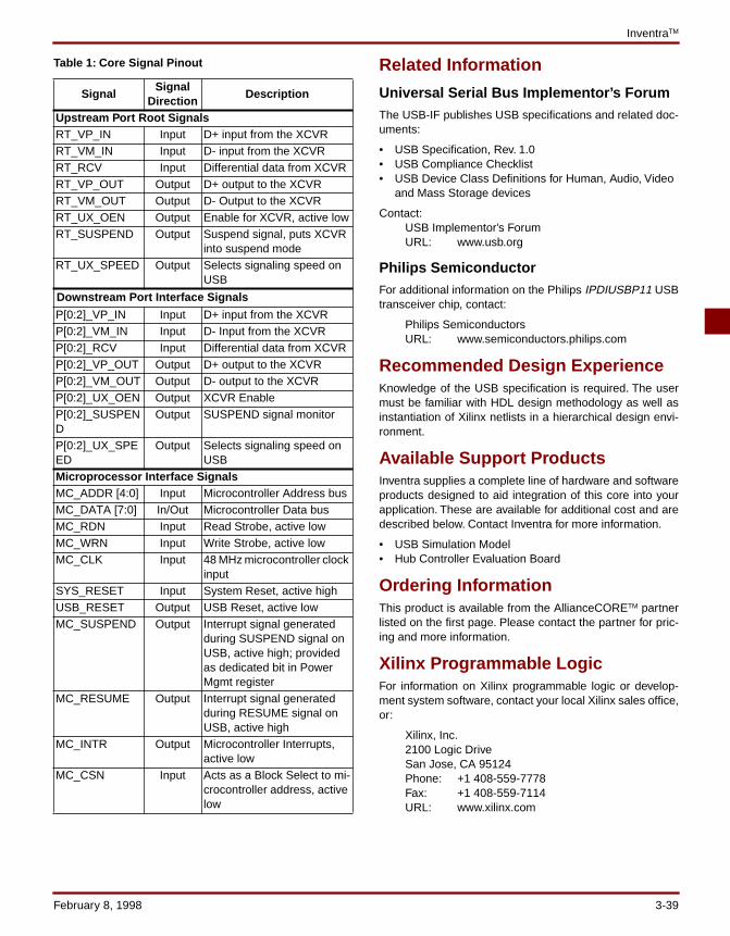
InventraTM
Table 1: Core Signal Pinout Related Information
Universal Serial Bus Implementor’s ForumThe USB-IF publishes USB specifications and related doc-uments:
• USB Specification, Rev. 1.0• USB Compliance Checklist• USB Device Class Definitions for Human, Audio, Video
and Mass Storage devices
Contact:USB Implementor’s ForumURL: www.usb.org
Philips SemiconductorFor additional information on the Philips IPDIUSBP11 USBtransceiver chip, contact:
Philips SemiconductorsURL: www.semiconductors.philips.com
Recommended Design ExperienceKnowledge of the USB specification is required. The usermust be familiar with HDL design methodology as well asinstantiation of Xilinx netlists in a hierarchical design envi-ronment.
Available Support ProductsInventra supplies a complete line of hardware and softwareproducts designed to aid integration of this core into yourapplication. These are available for additional cost and aredescribed below. Contact Inventra for more information.
• USB Simulation Model • Hub Controller Evaluation Board
Ordering InformationThis product is available from the AllianceCORETM partnerlisted on the first page. Please contact the partner for pric-ing and more information.
Xilinx Programmable LogicFor information on Xilinx programmable logic or develop-ment system software, contact your local Xilinx sales office,or:
Xilinx, Inc.2100 Logic DriveSan Jose, CA 95124Phone: +1 408-559-7778Fax: +1 408-559-7114URL: www.xilinx.com
SignalSignal
DirectionDescription
Upstream Port Root SignalsRT_VP_IN Input D+ input from the XCVRRT_VM_IN Input D- input from the XCVRRT_RCV Input Differential data from XCVRRT_VP_OUT Output D+ output to the XCVRRT_VM_OUT Output D- Output to the XCVRRT_UX_OEN Output Enable for XCVR, active lowRT_SUSPEND Output Suspend signal, puts XCVR
into suspend modeRT_UX_SPEED Output Selects signaling speed on
USB
Downstream Port Interface Signals
P[0:2]_VP_IN Input D+ input from the XCVRP[0:2]_VM_IN Input D- Input from the XCVRP[0:2]_RCV Input Differential data from XCVRP[0:2]_VP_OUT Output D+ output to the XCVRP[0:2]_VM_OUT Output D- output to the XCVRP[0:2]_UX_OEN Output XCVR EnableP[0:2]_SUSPEND
Output SUSPEND signal monitor
P[0:2]_UX_SPEED
Output Selects signaling speed on USB
Microprocessor Interface SignalsMC_ADDR [4:0] Input Microcontroller Address busMC_DATA [7:0] In/Out Microcontroller Data busMC_RDN Input Read Strobe, active lowMC_WRN Input Write Strobe, active lowMC_CLK Input 48 MHz microcontroller clock
inputSYS_RESET Input System Reset, active highUSB_RESET Output USB Reset, active lowMC_SUSPEND Output Interrupt signal generated
during SUSPEND signal on USB, active high; provided as dedicated bit in Power Mgmt register
MC_RESUME Output Interrupt signal generated during RESUME signal on USB, active high
MC_INTR Output Microcontroller Interrupts, active low
MC_CSN Input Acts as a Block Select to mi-crocontroller address, active low
February 8, 1998 3-39
3-Port USB Hub Controller
For general Xilinx literature, contact:
Phone: +1 800-231-3386 (inside the US)+1 408-879-5017 (outside the US)
E-mail: [email protected]
For AllianceCORETM specific information, contact:
Phone: +1 408-879-5381E-mail: [email protected]: www.xilinx.com/products/logicore/alliance/
tblpart.htm
3-40 February 8, 1998
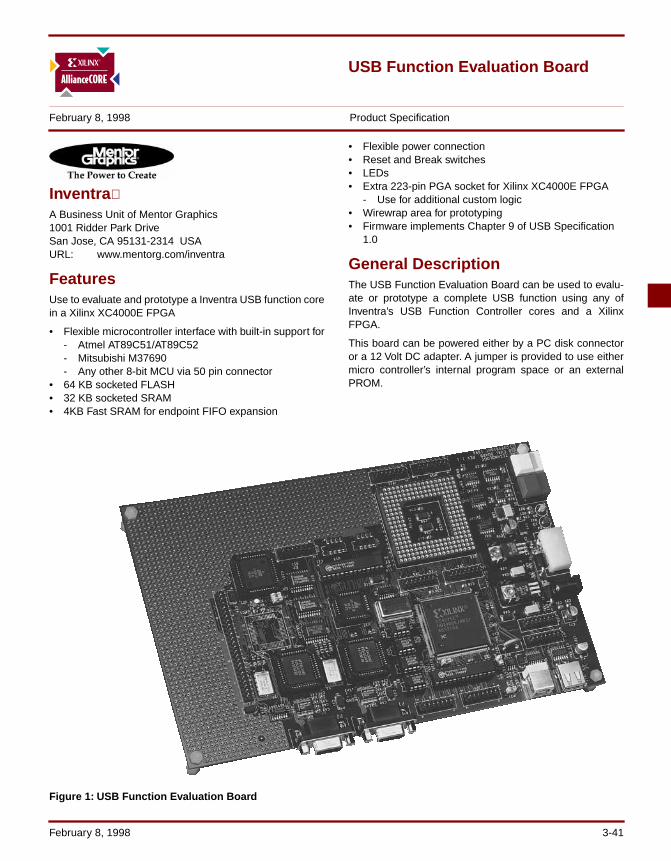
USB Function Evaluation Board
February 8, 1998 Product Specification
Inventra A Business Unit of Mentor Graphics 1001 Ridder Park DriveSan Jose, CA 95131-2314 USAURL: www.mentorg.com/inventra
FeaturesUse to evaluate and prototype a Inventra USB function corein a Xilinx XC4000E FPGA
• Flexible microcontroller interface with built-in support for- Atmel AT89C51/AT89C52- Mitsubishi M37690- Any other 8-bit MCU via 50 pin connector
• 64 KB socketed FLASH• 32 KB socketed SRAM• 4KB Fast SRAM for endpoint FIFO expansion
• Flexible power connection• Reset and Break switches• LEDs• Extra 223-pin PGA socket for Xilinx XC4000E FPGA
- Use for additional custom logic• Wirewrap area for prototyping• Firmware implements Chapter 9 of USB Specification
1.0
General DescriptionThe USB Function Evaluation Board can be used to evalu-ate or prototype a complete USB function using any ofInventra’s USB Function Controller cores and a XilinxFPGA.
This board can be powered either by a PC disk connectoror a 12 Volt DC adapter. A jumper is provided to use eithermicro controller’s internal program space or an externalPROM.
Figure 1: USB Function Evaluation Board
February 8, 1998 3-41
USB Function Evaluation Board
There are two serial ports available on the board. Port 1 isused to get debug information. The serial port can be con-nected to any terminal. (Usually a PC running terminalemulation software like PROCOMM or QLFAX ).
An upstream port is used to connect to the host computerwhile the downstream port can be used to connect toanother device.
Available Support ProductsInventra supplies a complete line of hardware and softwareproducts for USB system development. Contact Inventra formore information.
• USB Simulation Model• USB Cores for host, hub and function controllers.
Ordering InformationTo purchase or make further inquiries about this or otherInventra products, contact your local Mentor Graphics salesrepresentative, or Inventra directly.
Related Information
Xilinx Programmable LogicFor information on Xilinx programmable logic or develop-ment system software, contact your local Xilinx sales office,or:
Xilinx, Inc.2100 Logic DriveSan Jose, CA 95124Phone: +1 408-559-7778Fax: +1 408-559-7114URL: www.xilinx.com
For general Xilinx literature, contact:
Phone: +1 800-231-3386 (inside the US)+1 408-879-5017 (outside the US)
E-mail: [email protected]
For AllianceCORETM specific information, contact:
Phone: +1 408-879-5381E-mail: [email protected]: www.xilinx.com/products/logicore/alliance/
tblpart.htm
3-42 February 8, 1998
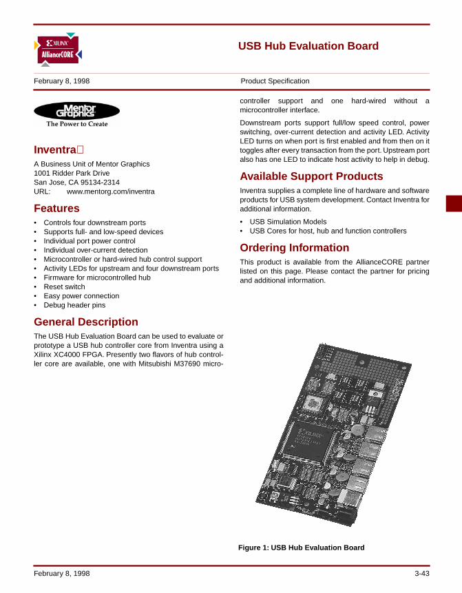
USB Hub Evaluation Board
February 8, 1998 Product Specification
Inventra A Business Unit of Mentor Graphics1001 Ridder Park DriveSan Jose, CA 95134-2314URL: www.mentorg.com/inventra
Features• Controls four downstream ports• Supports full- and low-speed devices• Individual port power control• Individual over-current detection• Microcontroller or hard-wired hub control support• Activity LEDs for upstream and four downstream ports• Firmware for microcontrolled hub• Reset switch• Easy power connection• Debug header pins
General DescriptionThe USB Hub Evaluation Board can be used to evaluate orprototype a USB hub controller core from Inventra using aXilinx XC4000 FPGA. Presently two flavors of hub control-ler core are available, one with Mitsubishi M37690 micro-
controller support and one hard-wired without amicrocontroller interface.
Downstream ports support full/low speed control, powerswitching, over-current detection and activity LED. ActivityLED turns on when port is first enabled and from then on ittoggles after every transaction from the port. Upstream portalso has one LED to indicate host activity to help in debug.
Available Support ProductsInventra supplies a complete line of hardware and softwareproducts for USB system development. Contact Inventra foradditional information.
• USB Simulation Models• USB Cores for host, hub and function controllers
Ordering InformationThis product is available from the AllianceCORE partnerlisted on this page. Please contact the partner for pricingand additional information.
Figure 1: USB Hub Evaluation Board
February 8, 1998 3-43
USB Hub Evaluation Board
Related Information
Xilinx Programmable LogicFor information on Xilinx programmable logic or develop-ment system software, contact your local Xilinx sales office,or:
Xilinx, Inc.2100 Logic DriveSan Jose, CA 95124Phone: +1 408-559-7778Fax: +1 408-559-7114URL: www.xilinx.com
For general Xilinx literature, contact:
Phone: +1 800-231-3386 (inside the US)+1 408-879-5017 (outside the US)
E-mail: [email protected]
For AllianceCORE™ specific information, contact:
Phone: +1 408-879-5381E-mail: [email protected]: www.xilinx.com/products/logicore/alliance/ tblpart.htm
3-44 February 8, 1998
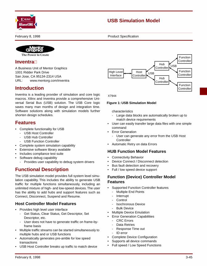
USB Simulation Model
February 8, 1998 Product Specification
Inventra A Business Unit of Mentor Graphics1001 Ridder Park DriveSan Jose, CA 95134-2314 USAURL: www.mentorg.com/inventra
IntroductionInventra is a leading provider of simulation and core logicmacros. Xilinx and Inventra provide a comprehensive Uni-versal Serial Bus (USB) solution. The USB Core logicsaves many man months of design and integration time.Software solutions along with simulation models furthershorten design schedules.
Features• Complete functionality for USB
- USB Host Controller- USB Hub Controller- USB Function Controller
• Complete system simulation capability• Extensive software library available• Includes compliance test suite• Software debug capability
- Provides user capability to debug system drivers
Functional DescriptionThe USB simulation model provides full system level simu-lation capability. This includes the ability to generate USBtraffic for multiple functions simultaneously, including anunlimited mixture of high- and low-speed devices. The userhas the ability to add hubs and support features such asConnect, Disconnect, Suspend and Resume.
Host Controller Model Features• Provides high level user interface
- Get Status, Clear Status, Get Descriptor, Set Descriptor, etc.
- User does not have to generate traffic on frame-by-frame basis
• Multiple traffic streams can be started simultaneously to multiple hubs and or USB functions
• Automatically generates pre-amble for low speed transactions
• USB Host Controller breaks up traffic to match device
characteristics- Large data blocks are automatically broken up to
match device requirements• User can easily transfer large data files with one simple
command• Error Generation
- User can generate any error from the USB Host Controller
• Automatic Retry on data Errors
HUB Function Model Features• Connectivity Behavior• Device Connect / Disconnect detection• Bus fault detection and recovery• Full / low speed device support
Function (Device) Controller Model Features• Supported Function Controller features
- Multiple End Points- Interrupt- Control- Isochronous Device- Bulk Device
• Multiple Device Emulation• Error Generation Capabilities
- CRC Errors- Data Retries- Response Time out- ID error
• Complete Device Configuration• Supports all device commands• Full speed / Low Speed Functions
High LevelInterface
USB
USBHub
Controller
HubController
HostController
FunctionController
FunctionController
FunctionController
X7944
Figure 1: USB Simulation Model
February 8, 1998 3-45
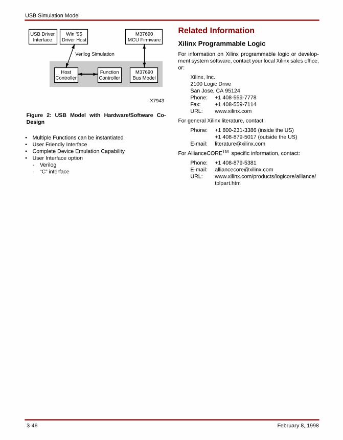
USB Simulation Model
• Multiple Functions can be instantiated• User Friendly Interface• Complete Device Emulation Capability• User Interface option
- Verilog- “C” interface
Related Information
Xilinx Programmable LogicFor information on Xilinx programmable logic or develop-ment system software, contact your local Xilinx sales office,or:
Xilinx, Inc.2100 Logic DriveSan Jose, CA 95124Phone: +1 408-559-7778Fax: +1 408-559-7114URL: www.xilinx.com
For general Xilinx literature, contact:
Phone: +1 800-231-3386 (inside the US)+1 408-879-5017 (outside the US)
E-mail: [email protected]
For AllianceCORETM specific information, contact:
Phone: +1 408-879-5381E-mail: [email protected]: www.xilinx.com/products/logicore/alliance/
tblpart.htm
Verilog Simulation
M37690Bus Model
HostController
FunctionController
USB DriverInterface
Win '95Driver Host
M37690MCU Firmware
X7943
Figure 2: USB Model with Hardware/Software Co-Design
3-46 February 8, 1998
Communications and Networking Products Table of Contents
February 8, 1998
Cell Assembler (CC-201) . . . . . . . . . . . . . . . . . . . . . . . . . . . . . . . . . . . . . . . . . . . .3-49Cell Delineation (CC-200) . . . . . . . . . . . . . . . . . . . . . . . . . . . . . . . . . . . . . . . . . . .3-53CRC10 Generator and Verifier (CC-130) . . . . . . . . . . . . . . . . . . . . . . . . . . . . . . . .3-57CRC32 Generator and Verifier (CC-131) . . . . . . . . . . . . . . . . . . . . . . . . . . . . . . . .3-61HDLC Protocol Core . . . . . . . . . . . . . . . . . . . . . . . . . . . . . . . . . . . . . . . . . . . . . . .3-65Reed-Solomon Decoder . . . . . . . . . . . . . . . . . . . . . . . . . . . . . . . . . . . . . . . . . . . . 3-71Reed-Solomon Encoder . . . . . . . . . . . . . . . . . . . . . . . . . . . . . . . . . . . . . . . . . . . . 3-77MT1F T1 Framer . . . . . . . . . . . . . . . . . . . . . . . . . . . . . . . . . . . . . . . . . . . . . . . . . .3-81UTOPIA Slave (CC-141) . . . . . . . . . . . . . . . . . . . . . . . . . . . . . . . . . . . . . . . . . . . .3-85Viterbi Decoder . . . . . . . . . . . . . . . . . . . . . . . . . . . . . . . . . . . . . . . . . . . . . . . . . . .3-91
3-47 February 8, 1998
Communications and Networking Products Table of Contents
3-48 February 8, 1998
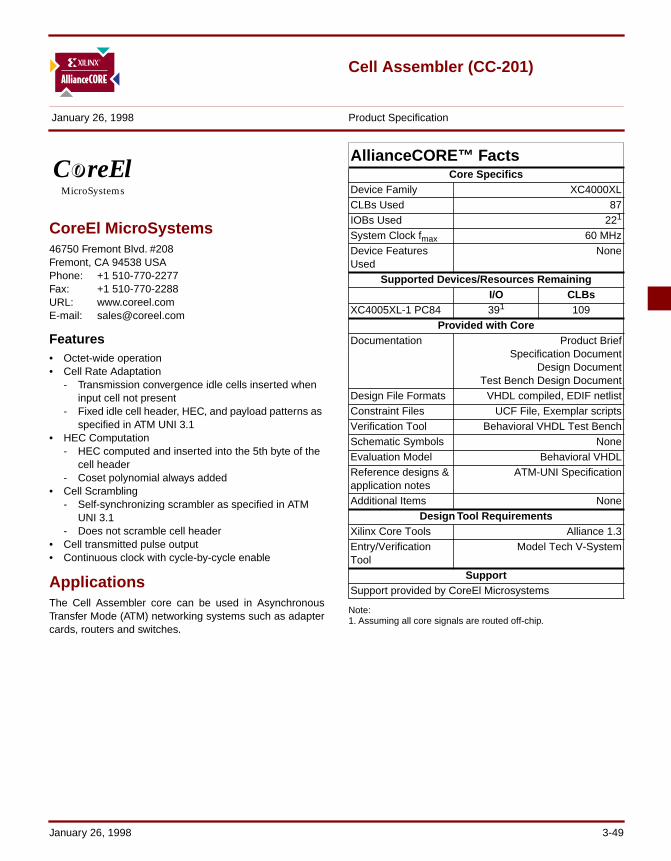
Cell Assembler (CC-201)
January 26, 1998 Product Specification
CoreEl MicroSystems46750 Fremont Blvd. #208Fremont, CA 94538 USAPhone: +1 510-770-2277Fax: +1 510-770-2288URL: www.coreel.comE-mail: [email protected]
Features• Octet-wide operation• Cell Rate Adaptation
- Transmission convergence idle cells inserted when input cell not present
- Fixed idle cell header, HEC, and payload patterns as specified in ATM UNI 3.1
• HEC Computation- HEC computed and inserted into the 5th byte of the
cell header- Coset polynomial always added
• Cell Scrambling- Self-synchronizing scrambler as specified in ATM
UNI 3.1- Does not scramble cell header
• Cell transmitted pulse output• Continuous clock with cycle-by-cycle enable
ApplicationsThe Cell Assembler core can be used in AsynchronousTransfer Mode (ATM) networking systems such as adaptercards, routers and switches.
Note:1. Assuming all core signals are routed off-chip.
CoreEloMicroSystems
AllianceCORE™ FactsCore Specifics
Device Family XC4000XLCLBs Used 87IOBs Used 221
System Clock fmax 60 MHzDevice Features Used
None
Supported Devices/Resources RemainingI/O CLBs
XC4005XL-1 PC84 391 109Provided with Core
Documentation Product BriefSpecification Document
Design DocumentTest Bench Design Document
Design File Formats VHDL compiled, EDIF netlistConstraint Files UCF File, Exemplar scriptsVerification Tool Behavioral VHDL Test BenchSchematic Symbols NoneEvaluation Model Behavioral VHDLReference designs & application notes
ATM-UNI Specification
Additional Items NoneDesign Tool Requirements
Xilinx Core Tools Alliance 1.3Entry/Verification Tool
Model Tech V-System
SupportSupport provided by CoreEl Microsystems
January 26, 1998 3-49

Cell Assembler (CC-201)
General DescriptionThe Cell Assembler carries out the functions required to beperformed in the receive stream of the Transmission Con-vergence sub-layer of an ATM Physical Layer processor.The input is a byte-aligned cell stream containing 52-bytecells with 4 bytes of header and 48 bytes of payload. TheCell Assembler computes the header Error Checksequence and inserts it in the fifth byte position of the out-going stream; thus creating the 53 byte output cell
Functional DescriptionThe Cell Assembler core is divided into blocks as shown inFigure 1: Controller, HEC Computation Module and Scram-bler. The Clock, ClockEnable and Reset_b signals are com-mon to all modules.
Controller BlockThe Controller inputs SOC_Input and Cell_present signalsand controls the data flow. It also inserts idle cells whenassigned cells are not present at the input. At the end ofevery cell, it checks the cell_present signal. If a cell ispresent, the controller asserts Read_Enable and reads itsheader. It deasserts Read_Enable for one clock when it
insertion of HEC in the stream, the controller reads pay-load. At the end of the cell it checks the cell present signalagain for deciding whether to insert idle cells or to transmitthe next valid cell.
HEC Computation ModuleThe HEC computation module computes HEC on first fourheader bytes, as indicated by the controller using the poly-nomial as specified in the ATM UNI 3.1 specification.
Scrambler ModuleThe scrambler module scrambles only payload octets usingthe polynomial as specified in the ATM UNI 3.1 specifica-tion.
Core ModificationsNormally, modifications are not possible by the user sincethe core is provided in a Xilinx netlist format. CoreEl canperform special modifications for additional charge. How-ever source code is available for additional cost where thecustomer can make modifications. Contact CoreEl Micro-systems for more information.
Data_output[7:0]
Read_Enable
SOC_output
Cell_txed
ScramblerHEC Computation Module
Controller
SOC_Input
Cell_present
Clock
Reset_b
ClockEnable HEC-Location
ScrEnable
HEC
Enable
ICData
HECByte
Data_Input[7:0]
MuxedData
8
8
8
8
8
8
X8303
Read_Enable
SOC_output
Cell_txed
Figure 1: Cell Assembler Core Block Diagram
3-50 January 26, 1998
CoreEl Microsystems
PinoutThe pinout is not fixed to any specific device I/O. Signalnames for the core are provided in the block diagramshown in Figure 1, and described in Table 1.
Table 1: Core Signal Pinout
Verification MethodsThis core has been used in larger ASICs and is siliconproven. The FPGA verification was done by back annotat-ing the implementation and simulating in a Model technol-ogy V-System environment.
The test bench was written in VHDL and provides fullyautomated verification.
Recommended Design ExperienceKnowledge of ATM technology and ATM Forum specifica-tions is needed. User should be familiar with HDL designmethodology including FPGA targeting. Using the test-bench requires familiarity with V-System of Model Technol-ogy.
Available Support ProductsCoreEl offers a test bench for verifying the core along witha complete line of ATM Core Cells for Xilinx FPGAs thatperform the following functions:
• UTOPIA Slave Interface• Cell Delineation• CRC-32• CRC-10
Ordering InformationFor information on this or other products mentioned in thisspecification, contact CoreEl Microsystems directly fromthe information provided on the front page.
Related Information
The ATM ForumThe ATM Forum publishes specifications regarding ATM.For more information, contact them as follows:
ATM ForumWorldwide Headquarters2570 West El Camino Real, Suite 304Mountain View, CA 94040-1313Tel: +1 650-949-6700Fax: +1 650-949-6705E-mail: [email protected]: www.atmforum.com
Xilinx Programmable LogicFor information on Xilinx programmable logic or develop-ment system software, contact your local Xilinx sales office,or:
Xilinx, Inc.2100 Logic DriveSan Jose, CA 95124Phone: +1 408-559-7778Fax: +1 408-559-7114URL: www.xilinx.com
For general Xilinx literature, contact:
Phone: +1 800-231-3386 (inside the US)+1 408-879-5017 (outside the US)
E-mail: [email protected]
For AllianceCORETM specific information, contact:
Phone: +1 408-879-5381E-mail: [email protected]: www.xilinx.com/products/logicore/alliance/
tblpart.htm
SignalSignal
DirectionDescription
Data_input[7:0] Input Input data bus for transferring in 52-byte cells
SOC_Input Input Start of cell indication for in-put cells
Cell_present Input Indicates cell is available to be read in; active high.
Clock Input Clock of up to 80 MHz com-patible with DS3, E3, STS-3c, and STS-12c applica-tions.
Reset_b Input Asynchronous Reset; active low.
Clock_enable Input Indicates clock cycles during which module is active.
Data_output[7:0]
Output Output data containing 53-byte cells with proper HEC.
Read_Enable Output Indicates that current clock cycle is being used to read in data; active high.
SOC_output Output Start of cell indication; active high.
Cell_txed Output Indicates completion of a cell transfer; active high.
January 26, 1998 3-51
Cell Assembler (CC-201)
3-52 January 26, 1998
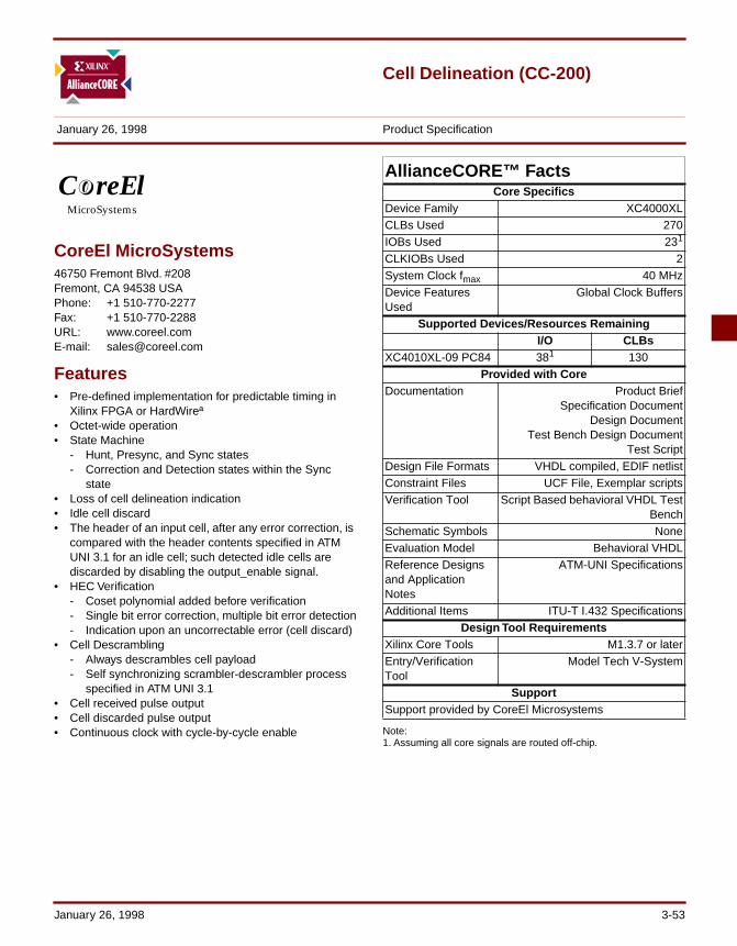
Cell Delineation (CC-200)
January 26, 1998 Product Specification
CoreEl MicroSystems46750 Fremont Blvd. #208Fremont, CA 94538 USAPhone: +1 510-770-2277Fax: +1 510-770-2288URL: www.coreel.comE-mail: [email protected]
Features• Pre-defined implementation for predictable timing in
Xilinx FPGA or HardWireª• Octet-wide operation• State Machine
- Hunt, Presync, and Sync states- Correction and Detection states within the Sync
state• Loss of cell delineation indication• Idle cell discard• The header of an input cell, after any error correction, is
compared with the header contents specified in ATM UNI 3.1 for an idle cell; such detected idle cells are discarded by disabling the output_enable signal.
• HEC Verification- Coset polynomial added before verification- Single bit error correction, multiple bit error detection- Indication upon an uncorrectable error (cell discard)
• Cell Descrambling- Always descrambles cell payload- Self synchronizing scrambler-descrambler process
specified in ATM UNI 3.1• Cell received pulse output• Cell discarded pulse output• Continuous clock with cycle-by-cycle enable Note:
1. Assuming all core signals are routed off-chip.
CoreEloMicroSystems
AllianceCORE™ FactsCore Specifics
Device Family XC4000XLCLBs Used 270IOBs Used 231
CLKIOBs Used 2System Clock fmax 40 MHzDevice Features Used
Global Clock Buffers
Supported Devices/Resources RemainingI/O CLBs
XC4010XL-09 PC84 381 130Provided with Core
Documentation Product BriefSpecification Document
Design DocumentTest Bench Design Document
Test ScriptDesign File Formats VHDL compiled, EDIF netlistConstraint Files UCF File, Exemplar scriptsVerification Tool Script Based behavioral VHDL Test
BenchSchematic Symbols NoneEvaluation Model Behavioral VHDLReference Designs and Application Notes
ATM-UNI Specifications
Additional Items ITU-T I.432 SpecificationsDesign Tool Requirements
Xilinx Core Tools M1.3.7 or laterEntry/Verification Tool
Model Tech V-System
SupportSupport provided by CoreEl Microsystems
January 26, 1998 3-53

Cell Delineation (CC-200)
ApplicationsThe Cell Delineation core can be used in AsynchronousTransfer Mode (ATM) networking systems such as adaptercards, routers and switches.
General DescriptionThe Cell Delineation core (CC-200) carries out the func-tions required in the receive stream of the TransmissionConvergence sub-layer of an ATM Physical Layer proces-sor (see Figure 1). The input is a byte-aligned cell streamcontaining 53-byte cells with 5 bytes of header and 48bytes of payload. CC-200 delineates cells as prescribed inITU specification I.432 and gives out header and payload.
Functional DescriptionThe Cell Delineation core is divided into eight blocks asshown in Figure 2: Data Buffer, HEC Computation Module,Correction Mask Generator, Cell Delineation StateMachine, Byte Counters, Idle Cell Detect Logic, Controllerand Descrambler.
Block DescriptionsThe clock, clockenable and reset_b signals are common toall blocks. The input data is passed through a nine-bytewide buffer and data at five particular buffer positions asindicated in Figure 2, and is fed to the Idle Cell Detect Logicblock, to determine whether the cell is assigned or idle.
The HEC computation module checks whether the HECcomputed over the first four header bytes matches with thedata in the fifth byte and indicates it using HECError signal.It uses the polynomial specified in ATM UNI 3.1.
Cell delineation is carried out by the Cell Delineation StateMachine and the Controller block which controls the mech-anism.
The Byte Counter keeps track of the number of bytes in acell (53). It is reset using Reset_cntr signal as well, which is
Byte
Stream
Cell
StreamFramerCircuit
CellDelineation
CoreX8336
Figure 1: Typical Application of Cell Delineation Core
Controller
Idle CellDetect Logic
CorrectionMask
Generator
Descrambler
ByteCounters
HECComputation
Module Remainder
Delineation State
HECError
ResetCounter
corr_enable
clockenable
clock
reset_b
Data_in
LCD
output_enable
cell_discard
cell_received
SOC_out
data_out
corr_enable
DescramblerEnable
CorrectionMask
ByteCount
ICFound
X8299
8 8
4
Data Buffer
5
8
CellDelineation
State Machine
Figure 2: Cell Delineation Core Block Diagram
3-54 January 26, 1998
CoreEl Microsystems
generated by the Cell Delineation State Machine. The ByteCounter outputs the byte count to the Controller block andthe expected location of the header to the Cell DelineationState Machine.
The correction mask generator block takes the remainderfrom the HEC computation module and finds out the cor-rection mask required in order to correct a single bit error inthe header.
The descrambler module descrambles only payload octetsusing the polynomial specified in ATM UNI 3.1. It descram-bles the cell payload using the self-synchronizing scram-bler procedure specified in ATM UNI 3.1. When an input cellheader matches the pattern specified for idle cells, the cellis discarded.
Basic OperationIn the initial Hunt state, the core performs a byte-by-bytesearch for possible header locations by applying the CRCcheck specified by the ATM Forum.
Upon detection of a possible valid header, the statemachine enters the Presync state where it verifies the valid-ity of the current cell delineation by checking the CRCHeader Error Check (HEC) sequence recorded in the 5thbyte of each cell. Upon a successful match for 6 consecu-tive cells, the state machine enters the Sync state in whichcell streams are given out along with a Start-of-cell indica-tion.
The Sync state consists of two sub-states called Correctionand Detection. In the Correction state, an attempt is madeto correct a cell header with a single bit error. Detection of amultiple bit error results in the cell being discarded. In eithercase the Detection state is entered where no attempt ismade to correct any cell header.
8 consecutive cells with correct header patterns would takethe state machine back to the Correction state. Seven con-secutive incorrect header patterns would take the statemachine back to the Hunt state.
Core ModificationsNormally, modifications are not possible by the user sincethe core is provided in a Xilinx netlist format. CoreEl canperform special modifications for additional charge. How-ever source code is available for additional cost where thecustomer can make modifications. Contact CoreEl Micro-systems for more information.
PinoutThe pinout is not fixed to any specific device I/O. Signalnames for the core are provided in the block diagramshown in Figure 1, and described in Table 1.
Table 1: Signal Core Pinout
Verification MethodsThis core has been used in larger ASICs and is siliconproven. The FPGA verification was done by back annotat-ing the implementation and simulating in a Model technol-ogy V-System environment.
The test bench was written in VHDL with very powerfulscripting capabilities and several scripts have been writtenfor verifying the implementation. Additional tests can beadded to the testbench by writing new scripts.
Recommended Design ExperienceKnowledge of ATM technology and ATM Forum specifica-tions is needed. User should be familiar with HDL designmethodology including FPGA targeting. Using the test-bench requires familiarity with V-System of Model Technol-ogy.
SignalSignal
DirectionDescription
data_in(7:0) Input Byte aligned input carrying a continuous stream of 53-byte cells.
reset_b Input Asynchronous reset; active low.
clock Input Clock of up to 80 MHz com-patible with E3, STS-3c, and STS-12c applications; uses 1 FPGA CLKIOB pin.
clockenable Input Indicates clock cycles during which module is active; uses 1 FPGA CLKIOB pin.
corr_enable Input Command indicating attempt to correct single bit errors in cell header; active high.
data_out(8:0) Output Output data containing 52-byte cells - 4 bytes header and 48 bytes payload.
SOC_out Output Start of cell indication; active high.
cell_received Output Indicates complete reception of a cell; active high. One clock wide pulse.
cell_discard Output Indicates cell has been dis-carded due to header error; active high. One clock wide pulse.
output_enable Output Indicates data on output bus is valid in current clock cycle; active high.
LCD Output Indicates loss of cell delinea-tion; active high.
January 26, 1998 3-55
Cell Delineation (CC-200)
Available Support ProductsCoreEl offers a test bench for verifying the core along witha complete line of ATM Core Cells for Xilinx FPGAs thatperform the following functions:
• UTOPIA Slave Interface• Cell Delineation• CRC-32• CRC-10
Ordering InformationFor information on this or other products mentioned in thisspecification, contact CoreEl Microsystems directly fromthe information provided on the front page.
Related Information
The ATM ForumThe ATM Forum publishes specifications regarding ATM.For more information, contact them as follows:
ATM ForumWorldwide Headquarters2570 West El Camino Real, Suite 304Mountain View, CA 94040-1313Tel: +1 650-949-6700Fax: +1 650-949-6705
E-mail: [email protected]: www.atmforum.com
Xilinx Programmable LogicFor information on Xilinx programmable logic or develop-ment system software, contact your local Xilinx sales office,or:
Xilinx, Inc.2100 Logic DriveSan Jose, CA 95124Phone: +1 408-559-7778Fax: +1 408-559-7114URL: www.xilinx.com
For general Xilinx literature, contact:
Phone: +1 800-231-3386 (inside the US)+1 408-879-5017 (outside the US)
E-mail: [email protected]
For AllianceCORETM specific information, contact:
Phone: +1 408-879-5381E-mail: [email protected]: www.xilinx.com/products/logicore/alliance/
tblpart.htm
3-56 January 26, 1998
CRC10 Generator and Verifier (CC-130)
January 26, 1998 Product Specification
CoreEl MicroSystems46750 Fremont Blvd. #208Fremont, CA 94538 USAPhone: +1 510-770-2277Fax: +1 510-770-2288URL: www.coreel.comE-mail: [email protected]
Features• Fully compatible with ITU-T Recommendation I.363 for
AAL3/4 and ATM OAM Cells• Single clock operation• Separate blocks for CRC10 Generator and CRC10
Verifier• Fully synchronous operation• Accepts 32 bit data per clock on which CRC10 is
computed• Performance up to 20 MHz giving a throughput of 640
Mbps• Fully synthesizable Register Transfer Level (RTL) VHDL
for FPGA available extra
ApplicationsThe CRC10 Generator and Verifier cores can be used intelecommunications and networking equipment includingATM, SONET and Ethernet systems.
General DescriptionThe CRC10 core is fully compliant to the ITU-T recommen-dation I.363 for AAL3/4 and ATM OAM Cells. The Coreincludes both CRC10 Generator and CRC10 Verifier mod-ules. The CRC10 core is fully synchronous with respect tothe input clock and is ideally suited to be in a Xilinx FPGAwith other high level functions.
Functional DescriptionThe CRC10 Generator and Verifier modules are dividedinto blocks as shown in Figure 1. Operation of each moduleis described below.
Note:
1. Assuming all core signals are routed off-chip.
Generator OperationThe CRC10 Generator computes and outputs the CRC10for a Cell Data. Init Signal sets the CRC10 output to all 0’s.The 32 Bit Trace Block computes the 32 bit intermediate
CoreEloMicroSystems
AllianceCORE™ FactsCore Specifics
Device Family Spartan XC4000XLCLBs - Generator:CLBs - Verifier:
8346
8346
IOBs - Generator:IOBs - Verifier:
461
371
461
371
CLKIOBs - Generator:CLKIOBs - Verifier:
11
11
11
11
System Clock fmax 20 MHz 20 MHzDevice Features Used N/A
Supported Devices/Resources RemainingI/O CLBs
XCS30 PQ208-4 (Gen)XCS30 PQ208-4 (Ver)
8392
493530
XC4013XL PQ160-2 (Gen)XC4013XL PQ160-2 (Ver)
8392
493530
Provided with CoreDocumentation Product Brief
Specification DocumentTest Bench Design Document
Test ScriptsDesign File Formats VHDL compiled, EDIF netlistConstraint Files Generator: crcgen.ucf
Verifier: crcver.ucfVerification Tool Script Based Behavioral
VHDL Test BenchSchematic Symbols NoneEvaluation Model Behavioral VHDLReference Designs & Application Notes
ITU-T I.363 Specification
Additional Items NoneDesign Tool Requirements
Xilinx Core Tools Alliance 1.3Entry/Verification Tool Model Tech V-System
SupportSupport provided by CoreEl Microsystems
January 26, 1998 3-57

CRC10 Generator and Verifier (CC-130)
CRC. The 22 Bit Trace Block computes another intermedi-ate 32 bit CRC. The 10 Most Significant Bits of the 32 BitTrace is selected as the CRC10 remainder when the Com-puteCRC is deasserted and the 10 Most Significant Bits ofthe 22 Bit Trace is selected as the CRC10 remainder whenthe ComputeCRC is asserted.
Verifier OperationThe CRC10 Verifier computes the CRC10 for the entire cellreceived and generates a CRCMatch signal if the result iszero. The Init Signal resets the CRCReg Outputs to zero.Once the whole cell is fed, the VerifyCRC signal must beasserted for one clock cycle in order to check the CRCRegValue for zero. If it is zero, the CRCMatch output signal isdriven high for one clock cycle.
Core ModificationsNormally, modifications are not possible by the user sincethe core is provided in a Xilinx netlist format. CoreEl canperform special modifications for additional charge. How-ever source code is available for additional cost where thecustomer can make modifications. Contact CoreEl Micro-systems for more information.
PinoutThe pinout is not fixed to any specific device I/O. Signalnames for each module are provided in the block diagramsshown in Figure 1, and described in Table 1.
Verification MethodsThis core has been used in larger ASICs and is siliconproven. The FPGA verification was done by back annotat-ing the implementation and simulating in a Model technol-ogy V-System environment.
The test bench was written in VHDL with very powerfulscripting capabilities and several scripts have been writtenfor verifying the implementation. Additional tests can beadded to the testbench by writing new scripts.
Recommended Design ExperienceKnowledge of error correction in network systems isneeded. User should be familiar with HDL design method-ology including FPGA targeting. Using the testbenchrequires familiarity with V-System of Model Technology.
Available Support ProductsCoreEl offers a test bench for verifying the core along witha complete line of ATM Core Cells for Xilinx FPGAs thatperform the following functions:
• UTOPIA Interface• Cell Delineation• Cell Assembly• CRC-32
Ordering InformationFor information on this or other products mentioned in thisspecification, contact CoreEl Microsystems directly fromthe information provided on the front page.
DataValidInit
Clock
Data(31:0)
DataValidInit
CRCREG
CE
CRCMatch
VerifyCRC
Logic 1 Logic 3
Logic 2
CRC10(9:0)
ComputeCRC
DataValidInit
Clock
Data(31:0)
DataValidInit
Clock
Data(31:0)
Logic
32-BitTrace
22-BitTrace
Generator Verifier X8334
Note: Reset signal is global for both modules and is not included in the diagrams.
Figure 1: CRC10 Generator and Verifier Block Diagrams
3-58 January 26, 1998
CoreEl Microsystems
Table 1: Core Signal Pinout
Related Information
The ATM ForumThe ATM Forum publishes specifications regarding ATM.For more information, contact them as follows:
ATM ForumWorldwide Headquarters2570 West El Camino Real, Suite 304Mountain View, CA 94040-1313Tel: +1 650-949-6700Fax: +1 650-949-6705E-mail: [email protected]: www.atmforum.com
Xilinx Programmable LogicFor information on Xilinx programmable logic or develop-ment system software, contact your local Xilinx sales office,or:
Xilinx, Inc.2100 Logic DriveSan Jose, CA 95124Phone: +1 408-559-7778Fax: +1 408-559-7114URL: www.xilinx.com
For general Xilinx literature, contact:
Phone: +1 800-231-3386 (inside the US)+1 408-879-5017 (outside the US)
E-mail: [email protected]
For AllianceCORETM specific information, contact:
Phone: +1 408-879-5381E-mail: [email protected]: www.xilinx.com/products/logicore/alliance/
tblpart.htm
SignalSignal
DirectionDescription
CRC10 Generator SignalsData(31:0) Input When DataValid is asserted,
Data should be dword of cur-rent cell for which CRC10 is computed.
DataValid Input Indicates input Data is valid and CRC10 to be computed for value on Data.
Init Input Init Signal sets initial CRC Value to 0; asserted on start of a new cell.
Clock Input Used to sample all other in-puts; uses FPGA CLKIOB pin.
Reset Input Resets outputs to 0; assert-ed on power-up/reset.
ComputeCRC Input When signal is sampled ac-tive, CRC10 output gives val-id 10 bit CRC to be transmitted with data; assert-ed along with last dword giv-en to CRC10 Generator.
CRC10(9:0) Output Indicates current CRC re-mainder of cell being pro-cessed.
CRC10 Verifier SignalsData(31:0) Input When DataValid is asserted,
Data should be dword of cur-rent cell for which CRC10 is computed.
DataValid Input Indicates input Data is valid and CRC10 to be computed for value on Data.
Init Input Init Signal sets initial CRC Value to 0; asserted on start of a new cell.
Clock Input Used to sample all other in-puts; uses FPGA CLKIOB pin.
Reset Input Resets outputs to 0; assert-ed on power-up/reset.
VerifyCRC Input When signal is sampled ac-tive, most significant 10 bits of CRC output is compared with zero. VerifyCRC should be asserted with 32 bit trailer of cell to find if cell was re-ceived without errors. Verify-CRC is asserted for one clock cycle if cell received is correct.
CRCMatch Output Asserted in response to Ver-ifyCRC if current CRC re-mainder matches zero.
SignalSignal
DirectionDescription
January 26, 1998 3-59

CRC10 Generator and Verifier (CC-130)
3-60 January 26, 1998
CRC32 Generator and Verifier (CC-131)
January 26, 1998 Product Specification
CoreEl MicroSystems46750 Fremont Blvd. #208Fremont, CA 94538 USAPhone: +1 510-770-2277Fax: +1 510-770-2288URL: www.coreel.comE-mail: [email protected]
Features• Fully compatible with ITU-T Recommendation I.363 for
AAL-5• Single clock operation• Separate blocks for CRC32 Generator and CRC32
Verifier• Fully synchronous operation• Performance up to 30 MHz giving a throughput of 960
Mbps• Accepts 32 bit data per clock on which CRC32 is
computed• Fully synthesizable Register Transfer Level (RTL) VHDL
source available extra
ApplicationsThe CRC32 Generator and Verifier cores can be used intelecommunications and networking equipment includingATM, SONET and Ethernet systems.
General DescriptionThe CRC32 core is fully compliant to the ITU-T recommen-dation I.363 for AAL-5. The Core includes CRC32 Genera-tor and CRC32 Verifier modules. The CRC32 core is ideallysuited to be designed into a Xilinx FPGA with other highlevel functions like Segmentation and Reassembly (SAR).
Note: 1. Assuming all core signals are routed off-chip.
CoreEloMicroSystems
AllianceCORE™ FactsCore Specifics
Device Family Spartan XC4000XLCLBs - Generator:CLBs - Verifier:
125127
125127
IOBs - Generator:IOBs - Verifier:
1001
691
1001
691
CLKIOBs - Generator:CLKIOBs - Verifier:
11
11
System Clock fmax 29 MHz 30 MHzDevice Features Used None
Supported Devices/Resources RemainingI/O1 CLBs
XCS30-4 PQ208 (Gen)XCS30-4 PQ208 (Ver)
2960
451449
XC4013XL-2 PQ160 (Gen)XC4013XL-2 PQ160 (Ver)
2960
451449
Provided with CoreDocumentation Product Brief
Specification DocumentTest Bench Design Document
Test ScriptsDesign File Formats VHDL compiled, EDIF netlistConstraint Files crcver.ucf crcgen.ucfVerification Tool Script Based Behavioral
VHDL Test BenchSchematic Symbols NoneEvaluation Model Behavioral VHDLReference Designs & Application Notes
ITU-T I.363 Specification
Additional Items NoneDesign Tool Requirements
Xilinx Core Tools Alliance 1.3Entry/Verification Tool Model Tech V-System
SupportSupport provided by CoreEl Microsystems
January 26, 1998 3-61
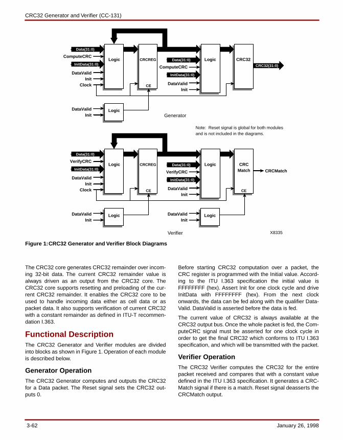
CRC32 Generator and Verifier (CC-131)
Generator
Verifier X8335
Note: Reset signal is global for both modulesand is not included in the diagrams.
CRC32(31:0)
DataValidInit
Clock
Data(31:0)
InitData(31:0)
DataValidInit
CRCREG
CE
Logic Logic CRC32
Logic
ComputeCRC
DataValidInit
Data(31:0)
InitData(31:0)
ComputeCRC
CRCMatch
DataValidInit
Clock
Data(31:0)
InitData(31:0)
DataValidInit
CRCREG
CE
Logic Logic CRCMatch
Logic DataValidInit
CE
Logic
VerifyCRC
DataValidInit
Data(31:0)
InitData(31:0)
VerifyCRC
The CRC32 core generates CRC32 remainder over incom-ing 32-bit data. The current CRC32 remainder value isalways driven as an output from the CRC32 core. TheCRC32 core supports resetting and preloading of the cur-rent CRC32 remainder. It enables the CRC32 core to beused to handle incoming data either as cell data or aspacket data. It also supports verification of current CRC32with a constant remainder as defined in ITU-T recommen-dation I.363.
Functional DescriptionThe CRC32 Generator and Verifier modules are dividedinto blocks as shown in Figure 1. Operation of each moduleis described below.
Generator OperationThe CRC32 Generator computes and outputs the CRC32for a Data packet. The Reset signal sets the CRC32 out-puts 0.
Before starting CRC32 computation over a packet, theCRC register is programmed with the Initial value. Accord-ing to the ITU I.363 specification the initial value isFFFFFFFF (hex). Assert Init for one clock cycle and driveInitData with FFFFFFFF (hex). From the next clockonwards, the data can be fed along with the qualifier Data-Valid. DataValid is asserted before the data is fed.
The current value of CRC32 is always available at theCRC32 output bus. Once the whole packet is fed, the Com-puteCRC signal must be asserted for one clock cycle inorder to get the final CRC32 which conforms to ITU I.363specification, and which will be transmitted with the packet.
Verifier OperationThe CRC32 Verifier computes the CRC32 for the entirepacket received and compares that with a constant valuedefined in the ITU I.363 specification. It generates a CRC-Match signal if there is a match. Reset signal deasserts theCRCMatch output.
Figure 1:CRC32 Generator and Verifier Block Diagrams
3-62 January 26, 1998
CoreEl Microsystems
Before starting CRC32 verification over a packet, the CRCregister must be programmed with the Initial valueFFFFFFFF (hex) as per ITU specification. Assert Init signalfor one clock cycle and drive InitData with FFFFFFFF (hex).From the next clock onwards, the data can be fed alongwith the qualifier DataValid. DataValid is the signal which isto be asserted before the Data is fed.
Once the whole packet is fed, VerifyCRC must be assertedfor one clock cycle in order to check for a CRC32 match. Ifit matches the constant value specified in I.363, the CRC-Match output signal will be driven high for one clock cycle.
Core ModificationsNormally, modifications are not possible by the user sincethe core is provided in a Xilinx netlist format. CoreEl canperform special modifications for additional charge. How-ever source code is available for additional cost where thecustomer can make modifications. Contact CoreEl Micro-systems for more information.
PinoutThe pinout is not fixed to any specific device I/O. Signalnames for each module are provided in the block diagramsshown in Figure 1, and described in Table 1.
Verification Methods This core has been used in larger ASICs and is siliconproven. The FPGA verification was done by back annotat-ing the implementation and simulating in a Model technol-ogy V-System environment.
The test bench was written in VHDL with very powerfulscripting capabilities and several scripts have been writtenfor verifying the implementation. Additional tests can beadded to the testbench by writing new scripts.
Recommended Design ExperienceKnowledge of error correction in network systems isneeded. User should be familiar with HDL design method-ology including FPGA targeting. Using the testbenchrequires familiarity with V-System of Model Technology.
Available Support ProductsCoreEl offers a test bench for verifying the core along witha complete line of ATM Core Cells for Xilinx FPGAs thatperform the following functions:
• UTOPIA Interface• Cell Delineation• Cell Assembly• CRC-10
Table 1: Core Signal Pinout
SignalSignal
DirectionDescription
CR32 Generator SignalsData(31:0) Input When DataValid is asserted,
Data should be next dword of AAL5 packet over which CRC32 is computed.
ComputeCRC Input When sampled active, CRC output is inverted; should be asserted along with last pay-load to find CRC remainder to be transmitted as last dword of AAL5 trailer.
InitData(31:0) Input When Init is asserted, InitDa-ta should be partial CRC re-sult for AAL5 packet processed so far.
DataValid Input Indicates input Data is valid and CRC32 to be computed for value on Data.
Init Input Loads CRC output with input InitData; asserted at start of new cell.
Clock Input Used to sample all other in-puts; uses FPGA CLKIOB pin.
Reset Input Resets outputs to 0; assert-ed on power-up/reset.
CRC32(31:0) Output Indicates current CRC re-mainder of AAL5 packet be-ing processed. During AAL5 packet processing, CRC32 should be sampled and val-ue stored in memory at each packet change. When same AAL5 packet processing re-sumes, stored CRC value should be driven onto InitDa-ta, and Init pulse should be generated to maintain CRC consistency over AAL5 pack-et.
CRC32 Verifier SignalsData(31:0) Input When DataValid is asserted,
Data should be next dword of AAL5 packet over which CRC32 is computed.
VerifyCRC Input When sampled active, CRC output is compared with an ITU I.363 defined constant; asserted with AAL5 trailer to find if AAL5 packet was re-ceived without errors.
January 26, 1998 3-63
CRC32 Generator and Verifier (CC-131)
Ordering InformationFor information on this or other products mentioned in thisspecification, contact CoreEl Microsystems directly fromthe information provided on the front page.
Related Information
The ATM ForumThe ATM Forum publishes specifications regarding ATM.For more information, contact them as follows:
ATM ForumWorldwide Headquarters2570 West El Camino Real, Suite 304Mountain View, CA 94040-1313Tel: +1 650-949-6700Fax: +1 650-949-6705E-mail: [email protected]: www.atmforum.com
Xilinx Programmable LogicFor information on Xilinx programmable logic or develop-ment system software, contact your local Xilinx sales office,or:
Xilinx, Inc.2100 Logic DriveSan Jose, CA 95124Phone: +1 408-559-7778Fax: +1 408-559-7114URL: www.xilinx.com
For general Xilinx literature, contact:
Phone: +1 800-231-3386 (inside the US)+1 408-879-5017 (outside the US)
E-mail: [email protected]
For AllianceCORETM specific information, contact:
Phone: +1 408-879-5381E-mail: [email protected]: www.xilinx.com/products/logicore/alliance/
tblpart.htm
InitData(31:0) Input When Init is asserted, InitDa-ta should be partial CRC re-sult for AAL5 packet processed so far.
DataValid Input Indicates input Data is valid and CRC32 to be computed for value on Data.
Init Input Loads CRC output with input InitData; asserted at start of new cell.
Clock Input Used to sample all other in-puts; uses FPGA CLKIOB pin.
Reset Input Resets outputs to 0; assert-ed on power-up/reset.
CRCMatch Output Asserted in response to Ver-ifyCRC if current CRC re-mainder matches an ITU I.363 defined constant.
SignalSignal
DirectionDescription
3-64 January 26, 1998
HDLC Protocol Core
February 8, 1998 Product Specification
Integrated Silicon Systems, Ltd.50 Malone RdBelfast BT9 5BSNorthern IrelandPhone: +44 1232 664664Fax: +44 1232 669664E-Mail: [email protected]: www.iss-dsp.com
Features• Single and double byte address recognition• 16 Bit (CRC-16) and 32 Bit (CRC-32) frame check
sequence• Asynchronous 8 bit input data interface, suitable for a
wide range of FIFOs• Compatible with ITU recommendation Q.921• Serial interface with external clocking for interfacing to
the PCM-highway• Transmission is synchronous to network interface with
back pressure mechanism. Buffering at the network interface not required.
• Supports transparent mode• Supports modular scaling of multiple HDLC channels
through parallel cores or core multiplexing• Supports data rate up to 50 Mbits/s
ApplicationsThe ISS HDLC Protocol core is a high performance imple-mentation suitable for a range of applications, includingX.25, Frame Relay and ISDN B-channel and D-channel.
Notes:1. CLB counts are for the example implementation
described in Table 1.2. Assuming all core signals are routed off-chip.
AllianceCORE™ FactsCore Specifics
Device Family XC4000XLCLBs Used Area optimized: 1291
Speed optimized: 1511
IOBs Used 272
CLKIOBs Used 2System Clock fmax Area optimized: 20 MHz
Speed optimized: 42 MHzDevice Features Used
N/A
Supported Devices/Resources RemainingI/O CLBs
XC4013XL-3 (area)XC4013XL-2 (speed)
1671
1671
447425
Provided with CoreDocumentation Core DocumentationDesign File Formats .xnf or.ngd netlist
VHDL source available extraConstraint Files .cstVerification Tool Test VectorsSchematic Symbols VHDL, VerilogEvaluation Model NoneReference designs & application notes
None
Additional Items NoneDesign Tool Requirements
Xilinx Core Tools Alliance 1.3Entry/Verification Tool
Synopsys VSS
SupportSupport provided by ISS.
February 8, 1998 3-65
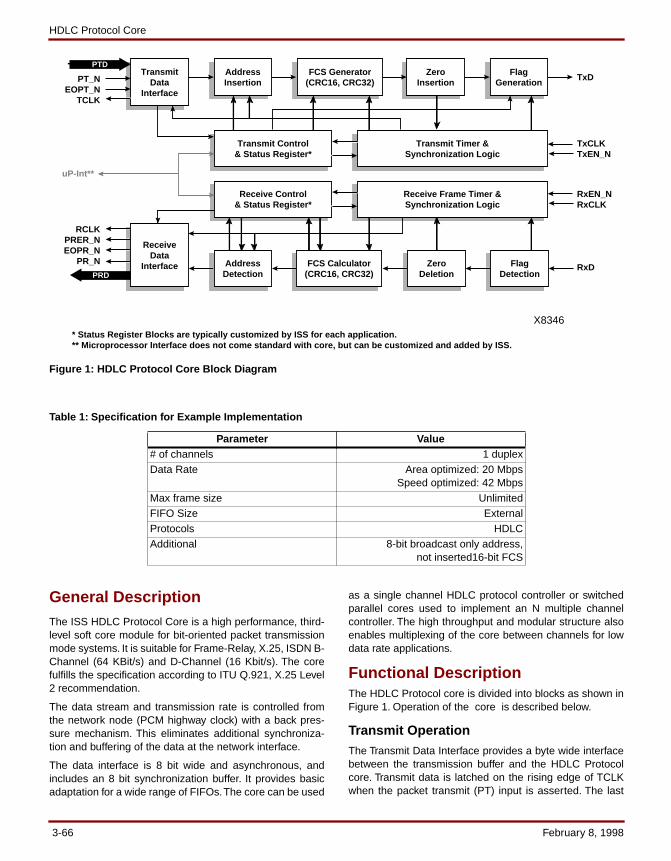
HDLC Protocol Core
uP-Int**
TransmitData
Interface
PT_NEOPT_N
TCLK
FCS Generator(CRC16, CRC32)
ZeroInsertion
FlagGeneration
TxDAddressInsertion
PTD
RxDFCS Calculator(CRC16, CRC32)
ZeroDeletion
FlagDetection
RCLKPRER_NEOPR_N
PR_N
PRD
ReceiveData
Interface
TxCLKTxEN_N
RxEN_NRxCLK
Transmit Control& Status Register*
Transmit Timer &Synchronization Logic
Receive Control& Status Register*
Receive Frame Timer &Synchronization Logic
AddressDetection
* Status Register Blocks are typically customized by ISS for each application.** Microprocessor Interface does not come standard with core, but can be customized and added by ISS.
X8346
Table 1: Specification for Example Implementation
General DescriptionThe ISS HDLC Protocol Core is a high performance, third-level soft core module for bit-oriented packet transmissionmode systems. It is suitable for Frame-Relay, X.25, ISDN B-Channel (64 KBit/s) and D-Channel (16 Kbit/s). The corefulfills the specification according to ITU Q.921, X.25 Level2 recommendation.
The data stream and transmission rate is controlled fromthe network node (PCM highway clock) with a back pres-sure mechanism. This eliminates additional synchroniza-tion and buffering of the data at the network interface.
The data interface is 8 bit wide and asynchronous, andincludes an 8 bit synchronization buffer. It provides basicadaptation for a wide range of FIFOs. The core can be used
as a single channel HDLC protocol controller or switchedparallel cores used to implement an N multiple channelcontroller. The high throughput and modular structure alsoenables multiplexing of the core between channels for lowdata rate applications.
Functional DescriptionThe HDLC Protocol core is divided into blocks as shown inFigure 1. Operation of the core is described below.
Transmit OperationThe Transmit Data Interface provides a byte wide interfacebetween the transmission buffer and the HDLC Protocolcore. Transmit data is latched on the rising edge of TCLKwhen the packet transmit (PT) input is asserted. The last
Parameter Value# of channels 1 duplexData Rate Area optimized: 20 Mbps
Speed optimized: 42 MbpsMax frame size UnlimitedFIFO Size ExternalProtocols HDLCAdditional 8-bit broadcast only address,
not inserted16-bit FCS
Figure 1: HDLC Protocol Core Block Diagram
3-66 February 8, 1998
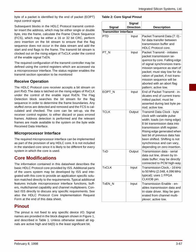
Integrated Silicon Systems, Ltd.
byte of a packet is identified by the end of packet (EOPT)input control signal.
Subsequent blocks in the HDLC Protocol transmit control-ler insert the address, which may be either single or doublebyte, into the frame, calculate the Frame Check Sequence(FCS), which may be either a 16 or 32 bit CRC, performzero insertion on the bit stream to ensure that the flagsequence does not occur in the data stream and add thestart and end flags to the frame. The transmit bit stream isclocked out on the rising edges of TxCLK under the controlof the enable signal TxEN.
The required configuration of the transmit controller may bedefined using the control registers which are accessed viaa microprocessor interface. The status register enables thetransmit section operation to be monitored
Receive OperationThe HDLC Protocol core receiver accepts a bit stream onport RxD. The data is latched on the rising edges of RxCLKunder the control of the enable input RxEN. The FlagDetection block searches the bit stream for the flagsequence in order to determine the frame boundaries. Anystuffed zeros are detected and removed and the FCS is cal-culated and checked. The core can be set-up, via thereceiver control register, to either discard or pass erroredframes. Address detection is performed and the relevantframes are made available to the system on the byte wideReceived Data Interface.
Microprocessor InterfaceThe required microprocessor interface can be implementedas part of the provision of any HDLC core. It is not includedin the standard core since it is likely to be different for everysystem in which the core is used.
Core ModificationsThe information contained in this datasheet describes thebasic HDLC Protocol core provided by ISS. Additional partsof the users system may be developed by ISS and inte-grated with this core to provide an application specific solu-tion matched directly to the requirements. Typical additionalfeatures include microprocessor interface functions, buff-ers, multichannel capability and channel multiplexers. Con-tact ISS directly to discuss any specific requirements. Seealso the HDLC Protocol Core Implementation RequestForm at the end of this data sheet.
PinoutThe pinout is not fixed to any specific device I/O. Signalnames are provided in the block diagram shown in Figure 1,and described in Table 1. Unless otherwise stated all sig-nals are active high and bit(0) is the least significant bit.
Table 2: Core Signal Pinout
SignalSignal
Direction DescriptionTransmitter InterfacePTD Input Packet Transmit Data (7: 0) -
for data transfer between transmission buffer and HDLC Protocol core.
PT_N Input Packet Transmit - initiates packet transmission se-quence by core. Falling edge of signal synchronizes trans-mission sequence as start of packet; must stay low for du-ration of packet, if not trans-mission sequence will be aborted with an abort flag pattern; active low.
EOPT_N Input End of Packet Transmit - in-dicates end of current trans-mitted packet; must be asserted during last byte pe-riod; active low.
TCLK Output Transmit Data Clock - byte clock with variable pulse width; loads (on rising edge) 8 bit transmission data into transmission shift register. Rising edge generated when last bit of previous data has been shifted. Shifting is not synchronous and can vary, depending on zero insertion.
TxD Output Transmission data - serial data out line, driven by tri-state buffer; may be directly connected to PCM high-way.
TxCLK Input Transmission Clock, - 16 kHz to 50 MHz (2.048, 4.096 MHz typical); uses 1 FPGA CLKIOB pin.
TxEN_N Input Transmission Enable - en-ables transmission data and tri-state driver. May be gen-erated from channel multi-plexer; active low.
February 8, 1998 3-67
HDLC Protocol Core
Verification MethodsThe core has been verified in Xilinx devices using post lay-out simulation across a wide range of configurations by
using input vector sequences compatible with many inter-national standards.
Available Support ProductsAlso available from ISS is a bit parallel (byte stuffed) ver-sion of this core for PPP applications.
Ordering InformationFor information on this or other products mentioned in thisspecification, contact Integrated Silicon Systems directlyfrom the information provided on the front page.
Related Information
International Telecommunications UnionInternational Telecommunications UnionPlace des NationsCH-1211Geneve 20SwitzerlandPhone: +41 22 730 51 11Fax: +41 22 733 72 56
Xilinx Programmable LogicFor information on Xilinx programmable logic or develop-ment system software, contact your local Xilinx sales office,or:
Xilinx, Inc.2100 Logic DriveSan Jose, CA 95214Phone: 408-559-7778Fax: 408-559-7114URL: www.xilinx.com
For general Xilinx literature, contact:
Phone: 800-231-3386 (inside the US)408-879-5017 (outside the US)
E-mail: [email protected]
For AllianceCORE specific information, contact:
Phone: 408-879-5381E-mail: [email protected]: www.xilinx.com/products/logicore/alliance/
tblpart.htm
Receiver InterfaceRCLK Output Receiver Data Clock - byte
clock with variable pulse width; pushes, on rising edge, 8 bit received data out of receiver shift register. Ris-ing edge generated when first bit of next byte is re-ceived.
PRER_N Output Packet Receive Error - indi-cates frame error. It is CRC results of received packet; active low.
EOPR_N Output End of Packet Received - in-dicates end of received packet, set during last re-ceived byte; active low.
PR_N Output Packet Received - indicates receipt of valid correct pack-et; stays low, until received packet is transferred; active low.
PRD Output Packet Receive Data (7:0) - provides data transfer be-tween receiver of HDLC Pro-tocol Core and receive buffer.
RxEN_N Input Receive Enable - enables masking of received data, may be generated by chan-nel multiplexer; active low.
RxCLK Input Receiver Clock, - 16 kHz up to 50 MHz (2.048, 4.096 MHz typical)
RxD Input Receive Data - is serial data in, latched with rising edge of RxCLK if RxEN is low.
SignalSignal
Direction Description
3-68 February 8, 1998

Integrated Silicon Systems, Ltd.
To: Integrated Silicon Systems, Inc.FAX: +44 1232 669664E-mail: [email protected]
From: _____________
Company: _____________
Name: _____________
Address: _____________
Country: _____________
Phone: _____________
Fax: __
E-mail: __
ISS configures and ships Xilinx netlist versions of theHDLC Protocol core customized to your specification.Please fill out and fax this form so ISS can respond with anappropriate quotation that includes performance and den-sity metrics for the target Xilinx FPGA
1. Number of required channels: ________________If more than one channel, storage is required for inactivechannel state. Is this storage to be on-chip or off-chip?
2. Please indicate:____ Serial data stream output with Zero-bit stuffed transpar-
ency____ Byte parallel data output with Octet stuffed transpar-
ency? 3. Data rate (per channel): __________
4. Available clocks: ________________
5. The bare core provides separate input, output and enableports for each configurable register. If a specific host bus inter-face is required, please specify the interface below.
6. The bare core provides byte-wide data ports with ByteTakenand ByteAvailable signals for use with external data FIFOs. Ifon-chip FIFOs are required with the core, please indicatewhich and specify their required size. Appropriate control anderror condition signals will then be available.
- Tx FIFO Size: ________________
- Rx FIFO Size: ________________
7. If there are any specific protocol requirements or deviationsfrom the HDLC specification, please detail them below.
8. Indicate required HDLC frame address field size:____ 8 bits fixed____ 16 bits fixed____ Programmable by control register bit
9. Indicate how address should be inserted into transmittedHDLC frames:____ Always____ Never____ Programmable by control register bit
10. Indicate if a programmable address is to be matched againstincoming frames:____ Always____ Never____ Programmable by control register bit
11. Indicate if the broadcast (all ones) address is recognized:____ Always____ Never____ Programmable by control register bit
12. Indicate if the broadcast address is recognized____ Yes____ No
13. Indicate if an all addresses mode (where all frames areaccepted and passed to the host____ Always (Note: this effectively disables all other forms of
address recognition.)____ Never____ Programmable by control register bit
14. Indicate if incoming address is stripped out of the packetbefore the data is passed through to the host:____ Always____ Never____ Programmable by control register bit
15. Indicate HDLC Frame Check Sequence (CRC) size:____ 16 bits fixed____ 32 bits fixed____ Programmable by control register bit
16. The default FCS polynomials are as follows. If alternativepolynomials are required, specify them in the space below.16 bit:X16+X12+X5+132 bit:X32+X26+X23+X22+X16+X12+X11+X10+X8+X7+X5+X4
+X2+X+1
17. Specify any additional requirements:
HDLC Protocol Core Implementation Request Form
February 8, 1998 3-69

HDLC Protocol Core
3-70 February 8, 1998
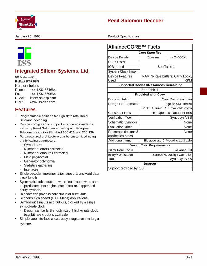
Reed-Solomon Decoder
January 26, 1998 Product Specification
Integrated Silicon Systems, Ltd.50 Malone RdBelfast BT9 5BSNorthern IrelandPhone: +44 1232 664664Fax: +44 1232 669664E-Mail: [email protected]: www.iss-dsp.com
Features• Programmable solution for high data rate Reed
Solomon decoding• Can be configured to support a range of standards
involving Reed Solomon encoding e.g. European Telecommunication Standard 300 421 and 300 429
• Paramaterized architecture can be customized using the following parameters:- Symbol size- Number of errors corrected- Number of erasures corrected- Field polynomial- Generator polynomial- Statistics gathering- Interfaces
• Single decoder implementation supports any valid data block length
• Systematic code structure where each code word can be partitioned into original data block and appended parity symbols
• Decoder can process continuous or burst data• Supports high speed (>300 Mbps) applications• Symbol-wide inputs and outputs, clocked by a single
symbol-rate clock- Design can be further optimized if higher rate clock
(e.g. bit rate clock) is available• Simple core interface allows easy integration into larger
systems
AllianceCORE™ FactsCore Specifics
Device Family Spartan XC4000XLCLBs Used
See Table 1IOBs UsedSystem Clock fmaxDevice Features Used
RAM, 3-state buffers, Carry Logic,RPM
Supported Devices/Resources RemainingSee Table 1
Provided with CoreDocumentation Core DocumentationDesign File Formats .ngd or XNF netlist
VHDL Source RTL available extraConstraint Files Timespec, .cst and.tnm filesVerification Tool Synopsys VSSSchematic Symbols NoneEvaluation Model NoneReference designs & application notes
None
Additional Items Bit-accurate C Model is availableDesign Tool Requirements
Xilinx Core Tools Alliance 1.3Entry/Verification Tool
Synopsys Design CompilerSynopsys VSS
SupportSupport provided by ISS.
January 26, 1998 3-71
Reed-Solomon Decoder
Table 1: Example Encoder Implementations
Applications• Digital video and audio broadcast.• Digital satellite broadcast.• Data storage and retrieval systems (e.g. hard disks,
CD-ROM etc.).
General DescriptionThe Reed Solomon decoder is a Xilinx FPGA-based corefor systems where data error detection/correction isrequired. The core implements the full functionality of ageneral Reed Solomon decoder and all necessary inter-face circuitry using a single Xilinx FPGA.
The source code version of the core is extremely flexibledue to its parameterized design, and can be rapidly config-ured for a wide variety of applications. The AllianceCOREfacts table shows density and performance metrics for a
specific implementation example. ISS will customize andprovide a Xilinx-specific implementation of the core tailoredto the needs of your application, (see Ordering Informa-tion).
PolynomialsA typical Code Generator Polynomial for the decoder is:
g(x) = (x +α0)(x + (1)(x +α2) …..(x +α15), where (=α02HEXand the number of parity symbols is 16.
A typical Field Generator Polynomial is:
p(x) = x8 + x4 + x3 + x2 + 1, where the Galois Field used isGF(28).
Functional DescriptionThe Reed-Solomon decoder core is partitioned into mod-ules as shown in Figure 1, and described below.
Example #1 Example #2 Example #3Correctable Errors 8 4 4Bits/Symbol 8 8 8Erasure Support? No No NoStatistics Gathering?
No Yes Yes
Xilinx Device XC4036XL-1 XCS40-3 XC4020E-2CLBs Used 941 740 740IOBs Used 19 24 24CLKIOBs Used 1 1 1System Clock fmax 40 MHz 20 MHz 20 MHzData Rate 320 Mbps 160 Mbps 160 MbpsCLBs Remaining 355 44 44I/O Remaining 268 200 200
Figure 1: Reed-Solomon Decoder Block Diagram - clock and reset signals omitted for clarity
DOUT (x:0)
X8337
Polynomial
Expansion
Syndrome
Calculation
FIFO
+
ERAS_FLG
I_P
DV_IN
I_PO
DV_OUT
CORR
ERR_CNT
ERAS_CNT
StasticsGathering
Error
Calculations
Key
Equation
SolverErrorLocation
Extraction
DIN (x:0)
3-72 January 26, 1998
Integrated Silicon Systems, Ltd.
Syndrome CalculationThe syndrome calculator accepts the received symbols. Itconsiders the symbol values as polynomial coefficients anddetermines if the series of symbols contained in a datablock form a valid code word for the particular Reed-Solomon code chosen. It evaluates the polynomial for 2tsyndrome values (where t is the number of correctable ran-dom errors) and detects whether the evaluations are zero(the data block is a code word) or non-zero (the data blockis not a code word). Any block that is not a code word hasbeen affected by errors.
Erasure Location ExtractionErasures are errors in known locations in the received datablock, and are flagged by other system functions such asthe receiver demodulator. Since the location of an erasureis known, the Reed-Solomon decoder only needs to deter-mine the magnitude of the error. This is unlike a randomerror where both error location and magnitude are calcu-lated. Therefore, for a given correction power, twice asmany erasures as random errors can be corrected.
A combination of erasures and random errors can be cor-rected provided the combination does not exceed the cor-rection power of the code, which is directly related to thenumber of parity symbols added to a data block.
Erasure symbols are flagged using the ERAS_FLG input,and the erasure location extraction block produces a poly-nomial representing erasure locations.
Polynomial ExpansionThe syndrome and erasure polynomials are combined inthis block to produce a single unified polynomial that can beprocessed by the key equation solver.
Key Equation SolverThe key equation relates the combined syndrome/erasurepolynomial with two error polynomials. The first is the errorlocator polynomial, which gives information about whichsymbols in the code word are in error. The second is theerror evaluator polynomial which, when further processedby the error calculation circuit, yields information regardingthe magnitude of each error. The key equation solver isresponsible for the derivation of the locator and evaluatorpolynomials.
Error CalculationThis component uses the error locator and evaluator poly-nomials to compute the error values for each symbol in thereceived data block. As each error value is computed, theappropriate received symbol is fetched from a code wordFIFO, which buffers the received symbols during thedecoding process. Each error value is simply added to thereceived symbol to produce the corrected symbol. (Note
that addition and subtraction are identical in the Finite Fieldarithmetic used in Reed-Solomon decoding.)
Statistics Gathering (Optional)This block receives information from the key equationsolver and the error calculator. It then computes statisticsregarding the degree of data corruption caused by thetransmission channel and the success of the decoder incorrecting this corruption. Typical statistical functionsinclude:
• Random error and erasure counts• Flags to indicate uncorrectable data blocks• Computation of bit error rates
This block along with the signals DV_IN, DV_OUT, CORR,ERR_CNT, and ERAS_CNT are optional. ISS can custom-ize and provide this for specific applications dependingupon your need.
ClockAll flipflops in the R-S decoder core operate on the risingedge of the input symbol rate clock CLK. Data inputs arelatched and outputs generated on the rising edge of theclock. CLB count of the core can be reduced if a higherclock rate, such as the bit rate clock, is available. In thiscase some of the hardware functions within the decodermay be clocked at the higher rate and reused multiple timesper symbol period, thus reducing the overall hardwarerequirements.
LatencyThe latency of the Reed-Solomon decoder is heavilydependent on:
• Data block length• Number of correctable errors• Whether uncorrectable data blocks are to be flagged• Degree by which the clock rate exceeds the symbol rate
The syndrome calculation and determination of block cor-rectability usually takes one data block length each since allsymbols in a block must be examined. Therefore, an uncor-rectable signal is valid once the entire block has passedthrough the statistics gathering circuit.
To ensure that the uncorrectable signal emerges from thedecoder simultaneous to the first data block symbol, thedata must be delayed by one block length. Hence, the Syn-drome Calculator and Statistics Gathering blocks accountfor two data block lengths of latency.
The remaining components contribute variable latencybased on the clock rate and the number of correctableerrors. It should be noted that these are only general guide-lines for decoder latency and, if low latency is a priority, itcan be achieved by trading off other design characteristicse.g. area. The latency of the Reed Solomon decoder exam-ple designs are shown in Table 1.
January 26, 1998 3-73
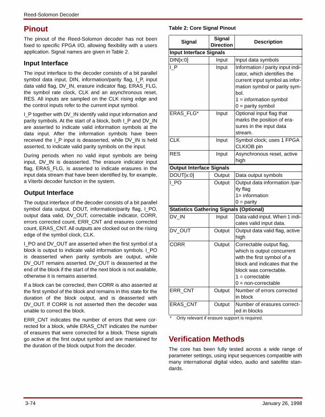
Reed-Solomon Decoder
PinoutThe pinout of the Reed-Solomon decoder has not beenfixed to specific FPGA I/O, allowing flexibility with a usersapplication. Signal names are given in Table 2.
Input InterfaceThe input interface to the decoder consists of a bit parallelsymbol data input, DIN, information/parity flag, I_P, inputdata valid flag, DV_IN, erasure indicator flag, ERAS_FLG,the symbol rate clock, CLK and an asynchronous reset,RES. All inputs are sampled on the CLK rising edge andthe control inputs refer to the current input symbol.
I_P together with DV_IN identify valid input information andparity symbols. At the start of a block, both I_P and DV_INare asserted to indicate valid information symbols at thedata input. After the information symbols have beenreceived the I_P input is deasserted, while DV_IN is heldasserted, to indicate valid parity symbols on the input.
During periods when no valid input symbols are beinginput, DV_IN is deasserted. The erasure indicator inputflag, ERAS_FLG, is asserted to indicate erasures in theinput data stream that have been identified by, for example,a Viterbi decoder function in the system.
Output InterfaceThe output interface of the decoder consists of a bit parallelsymbol data output, DOUT, information/parity flag, I_PO,output data valid, DV_OUT, correctable indicator, CORR,errors corrected count, ERR_CNT and erasures correctedcount, ERAS_CNT. All outputs are clocked out on the risingedge of the symbol clock, CLK.
I_PO and DV_OUT are asserted when the first symbol of ablock is output to indicate valid information symbols. I_POis deasserted when parity symbols are output, whileDV_OUT remains asserted. DV_OUT is deasserted at theend of the block if the start of the next block is not available,otherwise it is remains asserted.
If a block can be corrected, then CORR is also asserted atthe first symbol of the block and remains in this state for theduration of the block output, and is deasserted withDV_OUT. If CORR is not asserted then the decoder wasunable to correct the block.
ERR_CNT indicates the number of errors that were cor-rected for a block, while ERAS_CNT indicates the numberof erasures that were corrected for a block. These signalsgo active at the first output symbol and are maintained forthe duration of the block output from the decoder.
Verification MethodsThe core has been fully tested across a wide range ofparameter settings, using input sequences compatible withmany international digital video, audio and satellite stan-dards.
Table 2: Core Signal Pinout
SignalSignal
DirectionDescription
Input Interface SignalsDIN[x:0] Input Input data symbolsI_P Input Information / parity input indi-
cator, which identifies the current input symbol as infor-mation symbol or parity sym-bol.1 = information symbol0 = parity symbol
ERAS_FLG* Input Optional input flag that marks the position of era-sures in the input data stream.
CLK Input Symbol clock; uses 1 FPGA CLKIOB pin
RES Input Asynchronous reset, active high
Output Interface SignalsDOUT[x:0] Output Data output symbolsI_PO Output Output data information /par-
ity flag 1= information 0 = parity
Statistics Gathering Signals (Optional)DV_IN Input Data valid input. When 1 indi-
cates valid input data.DV_OUT Output Output data valid flag, active
highCORR Output Correctable output flag,
which is output concurrent with the first symbol of a block and indicates that the block was correctable.1 = correctable0 = non-correctable
ERR_CNT Output Number of errors corrected in block
ERAS_CNT Output Number of erasures correct-ed in blocks
* Only relevant if erasure support is required.
3-74 January 26, 1998
Integrated Silicon Systems, Ltd.
Recommended Design ExperienceFamiliarity with system standards relevant to the particularapplication is assumed. A basic understanding of ReedSolomon decoding is useful, but not essential.
Available Support ProductsA bit accurate C model of the Reed-Solomon decoder isavailable to assist in functional verification and system inte-gration.
ISS also supplies a complete line of peripheral cores thatcan be integrated with the Reed Solomon Encoder andDecoder cores for a complete forward error correction sys-tem using Xilinx FPGAs. For more information, contact ISSdirectly regarding:
• Block and convolution interleavers and deinterleavers• Scramblers and descramblers• Sync detection and insertion• Convolution encoders• Viterbi decoders
Ordering InformationThe Reed Solomon Decoder is available for purchasedirectly from ISS. The implementation will vary dependingupon your application. To determine what is required foryour system, fill out and fax the attached ImplementationRequest Form to ISS at +44 1232 669664.
Related Information
European Telecommunications Standards InstituteFor information on European digital broadcasting systemsstandards contact:
European Telecommunications Standards Institute6921 Sophia Antipolis CedexFrancePhone: +33 92 94 42 00Fax: +33 93 65 47 16
Xilinx Programmable LogicFor information on Xilinx programmable logic or develop-ment system software, contact your local Xilinx sales office,or:
Xilinx, Inc.2100 Logic DriveSan Jose, CA 95214Phone: 408-559-7778Fax: 408-559-7114URL: www.xilinx.com
For general Xilinx literature, contact:
Phone: 800-231-3386 (inside the US)408-879-5017 (outside the US)
E-mail: [email protected]
For AllianceCORE specific information, contact:
Phone: 408-879-5381E-mail: [email protected]: www.xilinx.com/products/logicore/alliance/
tblpart.htm
January 26, 1998 3-75

Reed-Solomon Decoder
3-76 January 26, 1998
To: Integrated Silicon Systems, Inc.FAX: +44 1232 669664E-mail: [email protected]
From:
Company:
Name:
Address:
Country:
Phone:
Fax:
E-mail:
ISS configures and ships Xilinx netlist versions of the ReedSolomon cores customized to your specification. Please fillout and fax this form so ISS can respond with an appropri-ate quotation that includes performance and density met-rics for the target Xilinx FPGA.
Implementation Issues
1. Indicate your exact requirement:______ Reed-Solomon encoder______ Reed-Solomon decoder______ Interleaver______ Deinterleaver
2. Maximum symbol rate: _______
3. Number of bits per symbol: _______
4. Indicate clock availability: ______ Bit clock______ Symbol Clock______ Both
5. Code generator polynomial (e.g. (x+a1)(x+a2)...)
6. Field generator polynomial (e.g. x8+x4+x3+x2+1)
7. Number of errors: ______
8. Codeword length/format (e.g. 204, 188):
9. Erasure support required:Yes ______ No ______
10. Indicate error statistics reporting requirement(s):______ Signal to show position of corrected errors______ Signal to show position of uncorrected blocks______ Other (please specify)
11. Indicate required control signals: low to high transition at start of codeword, high
to low transition at end of codeword low to high transitional start of codeword, high
to low transition at start of parity symbols delayed control signals available at output other (please specify)
12. Please specify any additional requirements:
13. If interleaver and/or deinterleaver functions arerequired, specify maximum depth of interleaving:
14. If the interleaver and/or deinterleaver are required isthe depth of interleaving to be programmable and ifso, to what degree?
Business Issues
15. Indicate timescales of requirement:a. date for decision ______b. date for placing order ______c. required delivery date ______
16. Indicate your area of responsibility:______ decision maker______ budget holder______ recommender
17. Has a budget been allocated for the purchase?Yes ______ No ______
18. What volume do you expect to ship of the product thatwill use this core? ______
19. What major factors will influence your decision?______ cost______ customization______ testing______ implementation size
20. Are you considering any other solutions?
Reed-Solomon Implementation Request Form
Reed-Solomon Encoder
January 12, 1998 Product Specification
Integrated Silicon Systems, Ltd.50 Malone RdBelfast BT9 5BSNorthern IrelandPhone: +44 1232 664664Fax: +44 1232 669664E-Mail: [email protected]: www.iss-dsp.com
Features• Programmable solution for high data rate Reed-
Solomon encoding• ISS can configure to support a range of standards
involving Reed-Solomon encoding, e.g. European Telecommunication Standard 300 421 and 300 429.
• Architecture can be customized using the following parameters:- Symbol size- Number of parity symbols- Field polynomial- Generator polynomial
• Single encoder implementation supports any valid data block length
• Systematic code structure where each code word can be partitioned into original data block and appended parity symbols
• Encoder can process continuous or burst data• Supports high speed (>570 Mbps) applications• Symbol-wide inputs and outputs, clocked by a single
symbol-rate clock• Simple interface allows easy integration into larger
system
Applications• Digital video and audio broadcast• Digital satellite broadcast• Data storage and retrieval systems (e.g. hard disks,
CD-ROM etc)
General DescriptionThe Reed-Solomon encoder is a Xilinx FPGA-based corefor systems where data error detection/correction is re-quired. The core implements the full functionality of a gen-eral Reed-Solomon encoder and all necessary interfacecircuitry using a single Xilinx FPGA.
The source code version of the core is extremely flexibledue to its parameterized design, and can be rapidly config-ured for a wide variety of applications. Table 1 shows den-sity and performance metrics for specific implementationexamples. ISS will customize and provide a Xilinx-specificimplementation of the core tailored to the needs of your ap-plication, (see Ordering Information).
AllianceCORE™ FactsCore Specifics
Device Family Spartan XC4000E/XLCLBs Used
See Table 1IOBs UsedSystem Clock fmaxDevice Features Used Carry Logic, RPM
Supported Devices/Resources RemainingSee Table 1
Provided with CoreDocumentation Core DocumentationDesign File Formats XNF or NGD netlistConstraint Files Timespec, .cst and .tnm filesVerification Tool Test VectorsSchematic Symbols NoneEvaluation Model NoneReference designs & application notes NoneAdditional Items Bit-accurate C Model is available
Design Tool RequirementsXilinx Core Tools Alliance 1.3Entry/Verification Tool
Synopsys Design CompilerSynopsys VSS
SupportSupport provided by ISS.
January 12, 1998 3-77
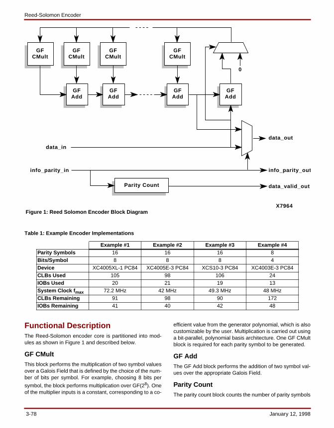
Reed-Solomon Encoder
Table 1: Example Encoder Implementations
Functional DescriptionThe Reed-Solomon encoder core is partitioned into mod-ules as shown in Figure 1 and described below.
GF CMultThis block performs the multiplication of two symbol valuesover a Galois Field that is defined by the choice of the num-ber of bits per symbol. For example, choosing 8 bits per
symbol, the block performs multiplication over GF(28). Oneof the multiplier inputs is a constant, corresponding to a co-
efficient value from the generator polynomial, which is alsocustomizable by the user. Multiplication is carried out usinga bit-parallel, polynomial basis architecture. One GF CMultblock is required for each parity symbol to be generated.
GF AddThe GF Add block performs the addition of two symbol val-ues over the appropriate Galois Field.
Parity CountThe parity count block counts the number of parity symbols
Example #1 Example #2 Example #3 Example #4Parity Symbols 16 16 16 8Bits/Symbol 8 8 8 4Device XC4005XL-1 PC84 XC4005E-3 PC84 XCS10-3 PC84 XC4003E-3 PC84CLBs Used 105 98 106 24IOBs Used 20 21 19 13System Clock f max 72.2 MHz 42 MHz 49.3 MHz 48 MHzCLBs Remaining 91 98 90 172IOBs Remaining 41 40 42 48
X7964
GFCMult
GFCMult
GFCMult
GFAdd
Parity Count
GFAdd
GFCMult
0
GFAdd
GFAdd
data_out
data_in
info_parity_in info_parity_out
data_valid_out
Figure 1: Reed Solomon Encoder Block Diagram
3-78 January 12, 1998
Integrated Silicon Systems, Ltd.
produced by the encoder for each block of data. The num-ber of valid parity symbols is twice the maximum number oferrors that are to be corrected. Any additional symbols pro-duced by the encoder are caused by spurious symbol val-ues that may exist between successive data blocks whenburst data is being processed. These spurious symbols aremarked in the output data stream by changing the value ofthe “data_valid_out” signal from high to low.
PinoutThe pinout of the Reed-Solomon Encoder has not beenfixed to specific FPGA I/O, allowing flexibility with a usersapplication. Signal names are shown in the block diagramof Figure 1 and in Table 2.
Table 2: Core Signal Pinout
Verification MethodsThe core has been fully tested across a wide range of pa-rameter settings, using input sequences compatible withmany international digital video, audio and satellite stan-dards.
Recommended Design ExperienceFamiliarity with system standards relevant to the particularapplication is assumed. A basic understanding of Reed-So-lomon encoding is useful, but not essential.
Available Support ProductsA C model of the Reed-Solomon encoder is available to as-sist in functional verification and system integration.
ISS also supplies a complete line of peripheral cores thatcan be integrated with the Reed Solomon Encoder and De-
coder cores for a complete forward error correction systemusing Xilinx FPGAs. For more information, contact ISS di-rectly regarding:• Block and convolution interleavers and deinterleavers• Scramblers and descramblers• Sync detection and insertion• Convolution encoders• Viterbi decoders
Ordering InformationThe Reed Solomon Encoder is available for purchase di-rectly from ISS. The implementation will vary dependingupon your application. To determine what is required foryour system, fill out and fax the attached ImplementationRequest Form to ISS at +44 1232 669664.
Related Information
European Telecommunications Standards InstituteFor information on European digital broadcasting systemsstandards contact:
European Telecommunications Standards Institute06921 Sophia Antipolis CedexFrancePhone : +33 92 94 42 00Fax : +33 93 65 47 16
Xilinx Programmable LogicFor information on Xilinx programmable logic or develop-ment system software, contact your local Xilinx sales office,or:
Xilinx, Inc.2100 Logic DriveSan Jose, CA 95124Phone: +1 408-559-7778Fax: +1 408-559-7114URL: www.xilinx.com
For general Xilinx literature, contact:Phone: +1 800-231-3386 (inside the US)
+1 408-879-5017 (outside the US)E-mail: [email protected]
For AllianceCORE™ specific information, contact:Phone: +1 408-879-5381E-mail: [email protected]: www.xilinx.com/products/logicore/alliance/
tblpart.htm
SignalSignal
DirectionDescription
DATA_IN [x:0] Input Input data symbolsINFO_PARITY_IN
InputMarks valid input infor-mation symbols
CLK Input Symbol ClockRESET
InputSystem Reset, active high
DATA_OUT [x:0] Output Output data symbolsINFO_PARITY_OUT
OutputMarks valid output infor-mation symbols
DATA_VALID_OUT
Output
Marks valid output infor-mation and parity sym-bols.
January 12, 1998 3-79
Reed-Solomon Encoder
3-80 January 12, 1998
To: Integrated Silicon Systems, Inc.FAX: +44 1232 669664E-mail: [email protected]
From:
Company:
Name:
Address:
Country:
Phone:
Fax:
E-mail:
ISS configures and ships Xilinx netlist versions of the ReedSolomon cores customized to your specification. Please fillout and fax this form so ISS can respond with an appropri-ate quotation that includes performance and density met-rics for the target Xilinx FPGA.
Implementation Issues
1. Indicate your exact requirement:______ Reed-Solomon encoder______ Reed-Solomon decoder______ Interleaver______ Deinterleaver
2. Maximum symbol rate: _______
3. Number of bits per symbol: _______
4. Indicate clock availability: __ ____ Bit clock______ Symbol Clock______ Both
5. Code generator polynomial (e.g. (x+a1)(x+a2)...)
6. Field generator polynomial (e.g. x8+x4+x3+x2+1)
7. Number of errors: ______
8. Codeword length/format (e.g. 204, 188):
9. Erasure support required:Yes ______ No ______
10. Indicate error statistics reporting requirement(s):______ Signal to show position of corrected errors______ Signal to show position of uncorrected blocks______ Other (please specify)
11. Indicate required control signals: low to high transition at start of codeword,high
to low transition at end of codeword low to high transitional start of codeword, high
to low transition at start of parity symbols delayed control signals available at output____ other (please specify)
12. Please specify any additional requirements:
13. If interleaver and/or deinterleaver functions arerequired, specify maximum depth of interleaving:
14. If the interleaver and/or deinterleaver are required isthe depth of interleaving to be programmable and ifso, to what degree?
Business Issues
15. Indicate timescales of requirement:a. date for decision ______b. date for placing order ______c. required delivery date ______
16. Indicate your area of responsibility:______ decision maker______ budget holder______ recommender
17. Has a budget been allocated for the purchase?Yes ______ No ______
18. What volume do you expect to ship of the product thatwill use this core? ______
19. What major factors will influence your decision?______ cost______ customization______ testing______ implementation size
20. Are you considering any other solutions?
Reed-Solomon Implementation Request Form
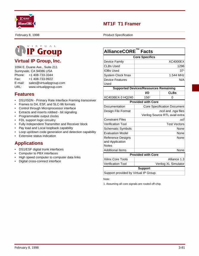
MT1F T1 Framer
February 8, 1998 Product Specification
Virtual IP Group, Inc.1094 E. Duane Ave., Suite 211 Sunnyvale, CA 94086 USAPhone: +1 408-733-3344Fax: +1 408-733-9922E-mail: [email protected]: www.virtualipgroup.com
Features• DS1/ISDN - Primary Rate Interface Framing transceiver• Frames to D4, ESF, and SLC-96 formats• Control through Microprocessor interface• Extracts and inserts robbed - bit signaling • Programmable output clocks• FDL support logic circuitry• Fully independent Transmitter and Receiver block• Pay load and Local loopback capability• Loop up/down code generation and detection capability• Extensive status indication
Applications• DS1/ESF digital trunk interfaces• Computer to PBX interfaces• High speed computer to computer data links• Digital cross-connect interface
Note:
1. Assuming all core signals are routed off-chip.
AllianceCORE ™ FactsCore Specifics
Device Family XC4000EXCLBs Used 1296IOBs Used 371
System Clock fmax 1.544 MHzDevice Features Used
N/A
Supported Devices/Resources RemainingI/O CLBs
XC4036EX-3 HQ240 1561 0Provided with Core
Documentation Core Specification DocumentDesign File Format .ncd and .nga files
Verilog Source RTL avail extraConstraint Files .ucfVerification Tool Test VectorsSchematic Symbols NoneEvaluation Model NoneReference Designs and Application Notes
None
Additional Items NoneProvided with Core
Xilinx Core Tools Alliance 1.3Verification Tool Verilog XL Simulator
SupportSupport provided by Virtual IP Group.
February 8, 1998 3-81
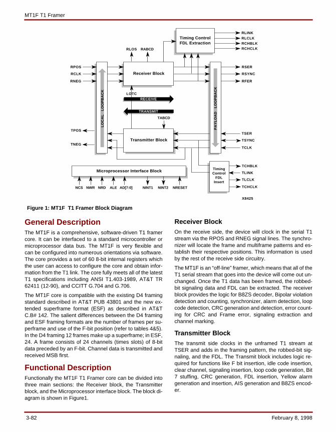
MT1F T1 Framer
General DescriptionThe MT1F is a comprehensive, software-driven T1 framercore. It can be interfaced to a standard microcontroller ormicroprocessor data bus. The MT1F is very flexible andcan be configured into numerous orientations via software.The core provides a set of 60 8-bit internal registers whichthe user can access to configure the core and obtain infor-mation from the T1 link. The core fully meets all of the latestT1 specifications including ANSI T1.403-1989, AT&T TR62411 (12-90), and CCITT G.704 and G.706.
The MT1F core is compatible with the existing D4 framingstandard described in AT&T PUB 43801 and the new ex-tended superframe format (ESF) as described in AT&TC.B# 142. The salient differences between the D4 framingand ESF framing formats are the number of frames per su-perframe and use of the F-bit position (refer to tables 4&5).In the D4 framing 12 frames make up a superframe; in ESF,24. A frame consists of 24 channels (times slots) of 8-bitdata preceded by an F-bit. Channel data is transmitted andreceived MSB first.
Functional DescriptionFunctionally the MT1F T1 Framer core can be divided intothree main sections: the Receiver block, the Transmitterblock, and the Microprocessor interface block. The block di-agram is shown in Figure1.
Receiver BlockOn the receive side, the device will clock in the serial T1stream via the RPOS and RNEG signal lines. The synchro-nizer will locate the frame and multiframe patterns and es-tablish their respective positions. This information is usedby the rest of the receive side circuitry.
The MT1F is an “off-line” framer, which means that all of theT1 serial stream that goes into the device will come out un-changed. Once the T1 data has been framed, the robbed-bit signaling data and FDL can be extracted. The receiverblock provides the logic for B8ZS decoder, Bipolar violationdetection and counting, synchronizer, alarm detection, loopcode detection, CRC generation and detection, error count-ing for CRC and Frame error, signaling extraction andchannel marking.
Transmitter BlockThe transmit side clocks in the unframed T1 stream atTSER and adds in the framing pattern, the robbed-bit sig-naling, and the FDL. The Transmit block includes logic re-quired for functions like F bit insertion, idle code insertion,clear channel, signaling insertion, loop code generation, Bit7 stuffing, CRC generation, FDL insertion, Yellow alarmgeneration and insertion, AIS generation and B8ZS encod-er.
Receiver Block
Timing ControlFDL Extraction
X8425
RPOS
RLOS
LOTC
NCS
RCLK
RNEG
TPOS
TNEG
TimingControl
FDLInsert
LO
CA
L
LO
OP
BA
CK
RSER
RSYNC
RFER
RLINKRLCLKRCHBLKRCHCLK
TSER
TCHBLK
TLINK
TLCLK
TCHCLK
TSYNC
TCLK
PA
YL
OA
D
LO
OP
BA
CK
Transmitter Block
Microprocessor Interface Block
RECEIVE
TRANSMIT
NWR NRD ALE NINT2NINT1AD[7:0] NRESET
TABCD
RABCD
Figure 1: MT1F T1 Framer Block Diagram
3-82 February 8, 1998
Virtual IP Group Inc.
Microprocessor Interface BlockThe Microprocessor interface contains a multiplexed ad-dress and data bus input and output data bus with outputenable which can be connected to either a Microcontrolleror Microprocessor.
Core ModificationsVirtual IP Group can perform modifications on the Xilinxnetlist version of this core for additional cost. This includesadding or removing blocks, or creating a different controllerinterface.
An Elastic Store function (in Verilog source format only) isavailable for additional cost. Contact Virtual IP Group formore information.
PinoutSignal names for the core are shown in Figure 1 and de-scribed in Table 1.
Verification MethodsThe FPGA core was tested through simulation.
Recommended Design ExperienceUsers should be familiar with T1 and related standards aswell as Xilinx design flows.
Ordering InformationThis product is available directly from Virtual IP Group, Inc.Please contact them for further information or pricing.
Related Information
Xilinx Programmable LogicFor information on Xilinx programmable logic or develop-ment system software, contact your local Xilinx sales office,or:
Xilinx, Inc.2100 Logic DriveSan Jose, CA 95124Phone: +1 408-559-7778Fax: +1 408-559-7114URL: www.xilinx.com
For general Xilinx literature, contact:
Phone: +1 800-231-3386 (inside the US)+1 408-879-5017 (outside the US)
E-mail: [email protected]
For AllianceCORE™ specific information, contact:
Phone: +1 408-879-5381E-mail: [email protected]: www.xilinx.com/products/logicore/alliance/
tblpart.htm
Table 1: Core Signal Pinout
Signal Signal
DirectionDescription
Transmitter Interface SignalsTPOS Output Transmit Bipolar Positive
Data: Updated on rising edge of TCLK. NRZ data is output when TCR1.7 = 1.
TNEG Output Transmit Bipolar Negative Data: Updated on rising edge of TCLK. Zero is output when TCR1.7 = 1.
TSER Input Transmit Serial Data: Trans-mit NRZ serial data, sampled on falling edge of TCLK.
TSYNC I/O Transmit Sync: A pulse on TSYNC will set either frame or multiframe boundaries. Can be programmed to out-put either a frame or multi-frame pulse; can also be set to output double-wide pulses at signaling frames.
TCLK Input Transmit Clock: 1.544 MHz Primary clock.
TCHBLK Output Transmit Channel Block: out-put; can be forced high or low during any of 24 T1 chan-nels.
TLINK Input Transmit Link Data: If en-abled, TLINK will be sampled during F-bit time on falling edge of TCLK for data inser-tion into either FDL stream (ESF) or Fs bit position (D4).
TLCLK Output Transmit Link Clock: 4 KHz demand clock for TLINK in-put.
TCHCLK Output Transmit Channel Clock: 192 KHz clock pulses high during LSB of each channel.
TABCD Input Transmit ABCD signaling: When enabled, data on this line is sampled on negedge of TCLK and inserted into the transmitted NRZ stream at signaling frames.
Receiver Interface SignalsRPOS Input Receive Bipolar Positive
Data Input: Sampled on fall-ing edge of RCLK. Tie to-gether to receive NRZ data and disable bipolar violation monitoring circuitry.
February 8, 1998 3-83
MT1F T1 Framer
RCLK Input Receive Clock: 1.544 MHz primary clock.
RNEG Input Receive Bipolar Negative Data Input: Sampled on fall-ing edge of RCLK.
RLINK Output Receive Link Data: Updated with FDL data (ESF) or Fs bits (D4) one RCLK before start of frame.
RLCLK Output Receive Link Clock: 4 KHz demand clock for RLINK.
RCHBLK Output Receive Channel Block: pro-grammable, can be forced high or low during any of 24 T1 channels.
RCHCLK Output Receive Channel Clock: 192 KHz clock, pulses high dur-ing LSB of each channel.
RSER Output Received NRZ Serial Data; updated on rising edges of RCLK.
RSYNC Output Receive Sync: An extracted pulse, (one RCLK wide) identifies either frame or mul-tiframe boundaries. Can also be set to output double-wide pulses on signaling frames.
RFER Output Receive Frame Error: High during F-bit time when Ft or Fs errors occur in D4 mode or when FPS or CRC errors occur in ESF mode. Low dur-ing resync.
RABCD Output Receive ABCD signaling: Outputs received signaling data.
LOTC/RLDS Output Receive Loss of Sync/Loss of Transmit Clock: dual func-tion. If CCR1.6=0, signal will toggle high when synchro-nizer is searching for T1 frame and multiframe. If CCR1.6=1, signal will toggle high when TCLK has not been toggled for 5µs.
Microprocessor Interface SignalsNCS Input Chip Select: must be low to
access internal registers (for read or write).
NWR Input Microprocessor Write signal.NRD Input Microprocessor Read signal.
Signal Signal
DirectionDescription
ALE Input Address Latch Enable: serves to demultiplex bus.
AD(7:0) In/Out Multiplexed Address/Data Bus: 8-bit multiplexed ad-dress/data input bus. For ad-dressing internal registers, only AD(5:0) are decoded.
NINT1 Output Receive Alarm Interrupt 1: Flags host controller during alarm conditions defined in Status Register 1.
NINT2 Output Receive Alarm Interrupt 2: Flags host controller during conditions defined in Status Register 2.
NRESET Input Reset input: Active low reset. Minimum pulse width should be one clock period (either TCLK/RCLK) duration.
Signal Signal
DirectionDescription
3-84 February 8, 1998
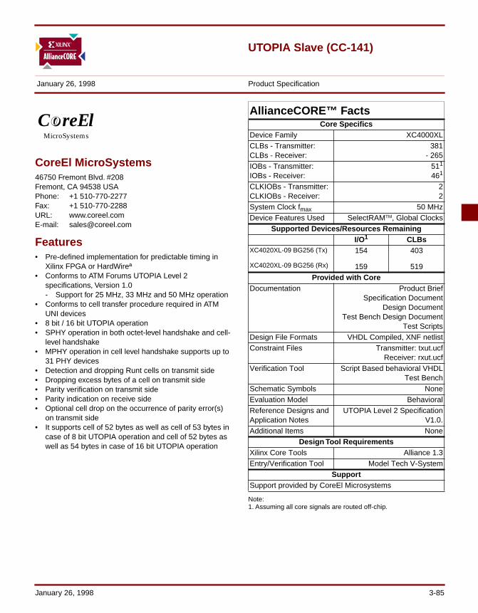
UTOPIA Slave (CC-141)
January 26, 1998 Product Specification
CoreEl MicroSystems46750 Fremont Blvd. #208Fremont, CA 94538 USAPhone: +1 510-770-2277Fax: +1 510-770-2288URL: www.coreel.comE-mail: [email protected]
Features• Pre-defined implementation for predictable timing in
Xilinx FPGA or HardWireª• Conforms to ATM Forums UTOPIA Level 2
specifications, Version 1.0- Support for 25 MHz, 33 MHz and 50 MHz operation
• Conforms to cell transfer procedure required in ATM UNI devices
• 8 bit / 16 bit UTOPIA operation• SPHY operation in both octet-level handshake and cell-
level handshake• MPHY operation in cell level handshake supports up to
31 PHY devices• Detection and dropping Runt cells on transmit side• Dropping excess bytes of a cell on transmit side• Parity verification on transmit side• Parity indication on receive side• Optional cell drop on the occurrence of parity error(s)
on transmit side• It supports cell of 52 bytes as well as cell of 53 bytes in
case of 8 bit UTOPIA operation and cell of 52 bytes as well as 54 bytes in case of 16 bit UTOPIA operation
Note: 1. Assuming all core signals are routed off-chip.
CoreEloMicroSystems
AllianceCORE™ FactsCore Specifics
Device Family XC4000XLCLBs - Transmitter: CLBs - Receiver:
381 - 265
IOBs - Transmitter: IOBs - Receiver:
511
461
CLKIOBs - Transmitter: CLKIOBs - Receiver:
22
System Clock fmax 50 MHzDevice Features Used SelectRAMTM, Global Clocks
Supported Devices/Resources RemainingI/O1 CLBs
XC4020XL-09 BG256 (Tx)
XC4020XL-09 BG256 (Rx)
154
159
403
519Provided with Core
Documentation Product BriefSpecification Document
Design DocumentTest Bench Design Document
Test ScriptsDesign File Formats VHDL Compiled, XNF netlistConstraint Files Transmitter: txut.ucf
Receiver: rxut.ucfVerification Tool Script Based behavioral VHDL
Test BenchSchematic Symbols NoneEvaluation Model BehavioralReference Designs and Application Notes
UTOPIA Level 2 SpecificationV1.0.
Additional Items NoneDesign Tool Requirements
Xilinx Core Tools Alliance 1.3Entry/Verification Tool Model Tech V-System
SupportSupport provided by CoreEl Microsystems
January 26, 1998 3-85
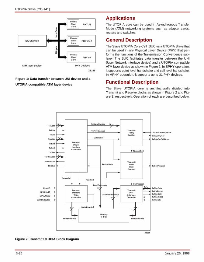
UTOPIA Slave (CC-141)
ApplicationsThe UTOPIA core can be used in Asynchronous TransferMode (ATM) networking systems such as adapter cards,routers and switches.
General DescriptionThe Slave UTOPIA Core Cell (SUC) is a UTOPIA Slave thatcan be used in any Physical Layer Device (PHY) that per-forms the functions of the Transmission Convergence sub-layer. The SUC facilitates data transfer between the UNI(User Network Interface device) and a UTOPIA compatibleATM layer device as shown in Figure 1. In SPHY operation,it supports octet level handshake and cell level handshake.In MPHY operation, it supports up to 31 PHY devices.
Functional DescriptionThe Slave UTOPIA core is architecturally divided intoTransmit and Receive blocks as shown in Figure 2 and Fig-ure 3, respectively. Operation of each are described below.
UtopiaSlaveCore
PHY #1
UtopiaSlaveCore
PHY #N-1
UtopiaSlaveCore
PHY #N
SAR/Switch
PHY DevicesATM layer device
Uto
pia
Inte
rfac
e
X8285
Figure 1: Data transfer between UNI device and a
UTOPIA compatible ATM layer device
Figure 2: Transmit UTOPIA Block Diagram
TransmitUtopia
InterfaceController
TransmitParity
Certifier
TransmitFIFOByte
Counter
TransmitMemory
WriteController
TransmitPHY
InterfaceController
16TxDataClocked
TxPrtyClocked
DataValid
AcceptData
RuntCellDataValid
Memory(FIFO)
DiscardOnPartyError
TxParityError
TxPrtyErrCellDrop
TxCellPresent
TxPhyDataTxUnderrunTxPhySoCTxPhyEnbBTxPhyClk
TxData
TxPrty
TxClk
TxAddr
TxEnb
TxSoC
TxClav
TxPhyAddr
TxOverrun
TCOCA
ResetB
UtWidth16
MPhyMode
CellOf52Bytes
WriteAddress ReadAddress
DataToMemory17
9
7
8
7
5
5
16
WriteEnable
DataFromMemory
CellPresent
DiscardCell
X8286
3-86 January 26, 1998

CoreEl Microsystems
Transmitter Block OperationTransmit UTOPIA provides an industry standard interfacebetween the ATM layer and a PHY device through a 216-Byte (4 cell) deep rate-matching buffer (FIFO). It supportsboth SPHY and MPHY modes of operation.
The Transmit interface is controlled by the ATM layer. TheATM layer provides an interface clock to the Transmit UTO-PIA core for synchronizing all interface transfers. Data flowin the transmit interface is in the same direction as the ATMenable. Signals TxEnb, TxData, TxSoC, and TxPrty aresampled on the rising edge of the TxClk.
It accepts 54, 53, or 52 byte cells from the ATM layer, writesthem into an internal FIFO with TxClk. Cells are read fromthe FIFO with TxPhyClk and sent to a cell processingdevice (cell processor) within the PHY. It detects and dis-cards runt cells and excess bytes. It also performs parity
check and gives the user the option of discarding the cellson the occurrence of parity errors.
The UTOPIA core indicates it can accept data using theTxClav signal, then the ATM layer drives data onto TxDataand asserts TxEnb. The UTOPIA core controls the flow ofdata via the TxClav signal.
Receive OperationThe Receive operation is controlled by the ATM layer. TheATM layer provides an interface clock to the UTOPIA coreto synchronize all transfers. The receive interface has dataflowing in the opposite direction as the ATM enable.
The ATM receive block generates all output signals on therising edge of RxClk. Signals RxData, RxSoC, RxPrty andRxEnb are sampled by the UTOPIA core on the rising edgeof RxClk.
Figure 3: Receive UTOPIA Block Diagram
ReceiveUtopia
InterfaceController
ReceiveFIFOByte
Counter
ReceiveMemory
ReadController
ReceivePHY
InterfaceController
DataReady
RuntCell
Read Data
Memory(FIFO)
RxPhyDataRxOverrunRxPhySoC
RxPhyEnbBRxPhyClk
RxPhyAddr
RxData
RxPrty
RxClk
RxEnB
RxSoC
RxClav
RxUnderrun
CellOf52Bytes
MPhyMode
UtWidth16
ResetB
ReadAddress WriteAddress
Data From Memory17
9
6
8
6
5
5
WriteEnable
DataToMemory
AcceptCell
X8287
16
RxAddr
ValidWrite
ReadData
January 26, 1998 3-87
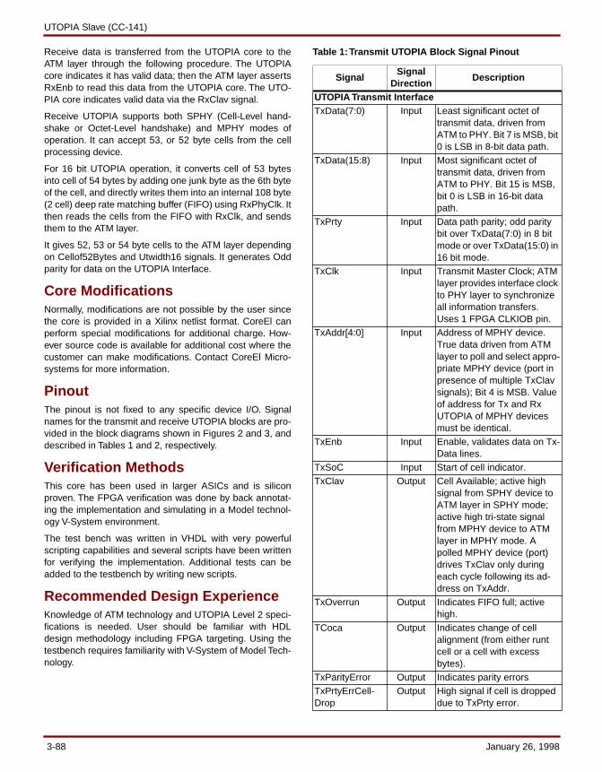
UTOPIA Slave (CC-141)
Receive data is transferred from the UTOPIA core to theATM layer through the following procedure. The UTOPIAcore indicates it has valid data; then the ATM layer assertsRxEnb to read this data from the UTOPIA core. The UTO-PIA core indicates valid data via the RxClav signal.
Receive UTOPIA supports both SPHY (Cell-Level hand-shake or Octet-Level handshake) and MPHY modes ofoperation. It can accept 53, or 52 byte cells from the cellprocessing device.
For 16 bit UTOPIA operation, it converts cell of 53 bytesinto cell of 54 bytes by adding one junk byte as the 6th byteof the cell, and directly writes them into an internal 108 byte(2 cell) deep rate matching buffer (FIFO) using RxPhyClk. Itthen reads the cells from the FIFO with RxClk, and sendsthem to the ATM layer.
It gives 52, 53 or 54 byte cells to the ATM layer dependingon Cellof52Bytes and Utwidth16 signals. It generates Oddparity for data on the UTOPIA Interface.
Core ModificationsNormally, modifications are not possible by the user sincethe core is provided in a Xilinx netlist format. CoreEl canperform special modifications for additional charge. How-ever source code is available for additional cost where thecustomer can make modifications. Contact CoreEl Micro-systems for more information.
PinoutThe pinout is not fixed to any specific device I/O. Signalnames for the transmit and receive UTOPIA blocks are pro-vided in the block diagrams shown in Figures 2 and 3, anddescribed in Tables 1 and 2, respectively.
Verification MethodsThis core has been used in larger ASICs and is siliconproven. The FPGA verification was done by back annotat-ing the implementation and simulating in a Model technol-ogy V-System environment.
The test bench was written in VHDL with very powerfulscripting capabilities and several scripts have been writtenfor verifying the implementation. Additional tests can beadded to the testbench by writing new scripts.
Recommended Design ExperienceKnowledge of ATM technology and UTOPIA Level 2 speci-fications is needed. User should be familiar with HDLdesign methodology including FPGA targeting. Using thetestbench requires familiarity with V-System of Model Tech-nology.
Table 1: Transmit UTOPIA Block Signal Pinout
SignalSignal
DirectionDescription
UTOPIA Transmit InterfaceTxData(7:0) Input Least significant octet of
transmit data, driven from ATM to PHY. Bit 7 is MSB, bit 0 is LSB in 8-bit data path.
TxData(15:8) Input Most significant octet of transmit data, driven from ATM to PHY. Bit 15 is MSB, bit 0 is LSB in 16-bit data path.
TxPrty Input Data path parity; odd parity bit over TxData(7:0) in 8 bit mode or over TxData(15:0) in 16 bit mode.
TxClk Input Transmit Master Clock; ATM layer provides interface clock to PHY layer to synchronize all information transfers. Uses 1 FPGA CLKIOB pin.
TxAddr[4:0] Input Address of MPHY device. True data driven from ATM layer to poll and select appro-priate MPHY device (port in presence of multiple TxClav signals); Bit 4 is MSB. Value of address for Tx and Rx UTOPIA of MPHY devices must be identical.
TxEnb Input Enable, validates data on Tx-Data lines.
TxSoC Input Start of cell indicator.TxClav Output Cell Available; active high
signal from SPHY device to ATM layer in SPHY mode; active high tri-state signal from MPHY device to ATM layer in MPHY mode. A polled MPHY device (port) drives TxClav only during each cycle following its ad-dress on TxAddr.
TxOverrun Output Indicates FIFO full; active high.
TCoca Output Indicates change of cell alignment (from either runt cell or a cell with excess bytes).
TxParityError Output Indicates parity errorsTxPrtyErrCell-Drop
Output High signal if cell is dropped due to TxPrty error.
3-88 January 26, 1998
CoreEl Microsystems
Table 2: Receive UTOPIA Block Signal PinoutSignal
Signal Direction
Description
PHY Layer Transmit InterfaceTxCellPresent Output Indication to cell processor of
presence of a complete cell in FIFO.
TxPhyData(7:0) Output Data output to cell processor; bit 7 is MSB, bit 0 is LSB.
TxUnderrun Output Indicates FIFO empty; active high.
TxPhySoC Output Start of cell indication to cell processor.
TxPhyEnbB Input Read enable; active low. Indi-cates valid data present on TxPhyData.
TxPhyClk Input Cell Clock, from cell proces-sor; synchronizes all informa-tion transfers with UTOPIA core. Uses 1 FPGA CLKIOB pin.
Configuration SignalsTxPhyAddr(4:0) Input PHY device address; provid-
ed by UNI device.ResetB Input Power-on reset; active low.UtWidth16 Input Indicates 16 bit data path; ac-
tive high.MPhyMode Input MPHY mode indicator; active
high.CellOf52Bytes Input Indicates cells of 52 bytes;
active high. Low value = cell of 53 bytes when UtWidth16 is low, and = 54 bytes when UtWidth16 is high.
DiscardOnPrty-Error
Input Indicates cells are discarded on occurrence of parity error; active high
SignalSignal
DirectionDescription
UTOPIA Receive InterfaceRxData(7:0) Output Low octet of receive data
from PHY to ATM; tristated when device (port) not select-ed by UTOPIA core. Bit 7 is MSB, bit 0 is LSB for 8-bit data path.
RxData(15:8) Output High octet of receive data from PHY to ATM; tristated when device (port) not select-ed by UTOPIA core. Bit 15 is MSB, bit 0 is LSB for 16-bit data path.
RxPrty Output Tristated
Data path parity; odd parity bit over RxData(7:0) in 8 bit mode or over RxData(15:0) in 16 bit mode. Tristated when device (port) not select-ed by UTOPIA core.
RxClk Input Clock from ATM to PHY; syn-chronizes all transfers Uses 1 FPGA CLKIOB pin.
RxEnb Input Receive Enable; validates data on RxData.
RxSoC Output Tristated
Start of cell. Tristated for mul-tiple PHYs, and enabled only in cycles following those with RxEnb asserted.
RxClav Output Tristated
Cell Available. Active high signal from SPHY device to ATM layer in SPHY mode. In MPHY mode, it is active high tri-state signal from MPHY device to ATM layer. Polled MPHY device (port) drives RxClav only during cycle fol-lowing one with its address on RxAddr lines.
RxUnderrun Output FIFO empty indicator; active high.
RxAddr[4:0] Input MPHY device address. True data from ATM to MPHY lay-er to poll and select appropri-ate MPHY device (port in presence of multiple RxClav signals). Bit 4 is MSB. Value of address for both Tx and Rx UTOPIA of MPHY devices must be identical.
January 26, 1998 3-89
UTOPIA Slave (CC-141)
Available Support ProductsCoreEl offers a test bench for verifying the SUC along witha complete line of ATM Core Cells for Xilinx FPGAs thatperform the following functions:
• Cell Delineation• Cell Stream Assembly• CRC-32• CRC-10
Ordering InformationFor information on this or other products mentioned in thisdatasheet, contact CoreEl Microsystems directly from theinformation provided on the front page.
Related Information
The ATM ForumThe ATM Forum publishes specifications regarding ATM.For more information, contact them as follows:
ATM ForumWorldwide Headquarters2570 West El Camino Real, Suite 304Mountain View, CA 94040-1313Tel: +1 650-949-6700Fax: +1 650-949-6705E-mail: [email protected]: www.atmforum.com
Xilinx Programmable LogicFor information on Xilinx programmable logic or develop-ment system software, contact your local Xilinx sales office,or:
Xilinx, Inc.2100 Logic DriveSan Jose, CA 95124Phone: +1 408-559-7778Fax: +1 408-559-7114URL: www.xilinx.com
For general Xilinx literature, contact:
Phone: +1 800-231-3386 (inside the US)+1 408-879-5017 (outside the US)
E-mail: [email protected]
For AllianceCORETM specific information, contact:
Phone: +1 408-879-5381E-mail: [email protected]: www.xilinx.com/products/logicore/alliance/
tblpart.htm
SignalSignal
DirectionDescription
PHY Layer Receive InterfaceRxPhyData(7:0) Input Data input from cell proces-
sor. Bit 7 is MSB, bit 0 is LSB.RxOverrun Output FIFO full indicator; active
high.RxPhySoC Input Start of cell indication from
cell processor.RxPhyClk Input Cell Clock from cell proces-
sor; synchronizes all trans-fers with UTOPIA core. Uses 1 FPGA CLKIOB pin.
RxPhyEnbB Input Indicates valid data on Rx-PhyData; active low.
Configuration SignalsRxPhyAddr (4:0) Input PHY device address; provid-
ed by UNI device.CellOf52Bytes Input Indicates cells of 52 bytes;
active high. Low value = cell of 53 bytes when UtWidth16 is low, and = 54 bytes when UtWidth16 is high.
MPhyMode Input MPHY mode indicator; active high.
UtWidth16 Input Indicates 16 bit data path; ac-tive high.
ResetB Input Power-on reset; active low.UTOPIA Receive InterfaceRxData(7:0) Output Low octet of receive data
from PHY to ATM; tristated when device (port) not select-ed by UTOPIA core. Bit 7 is MSB, bit 0 is LSB for 8-bit data path.
RxData(15:8) Output High octet of receive data from PHY to ATM; tristated when device (port) not select-ed by UTOPIA core. Bit 15 is MSB, bit 0 is LSB for 16-bit data path.
RxPrty Output
Tristated
Data path parity; odd parity bit over RxData(7:0) in 8 bit mode or over RxData(15:0) in 16 bit mode. Tristated when device (port) not select-ed by UTOPIA core.
RxClk Input Clock from ATM to PHY; syn-chronizes all transfers Uses 1 FPGA CLKIOB pin.
3-90 January 26, 1998
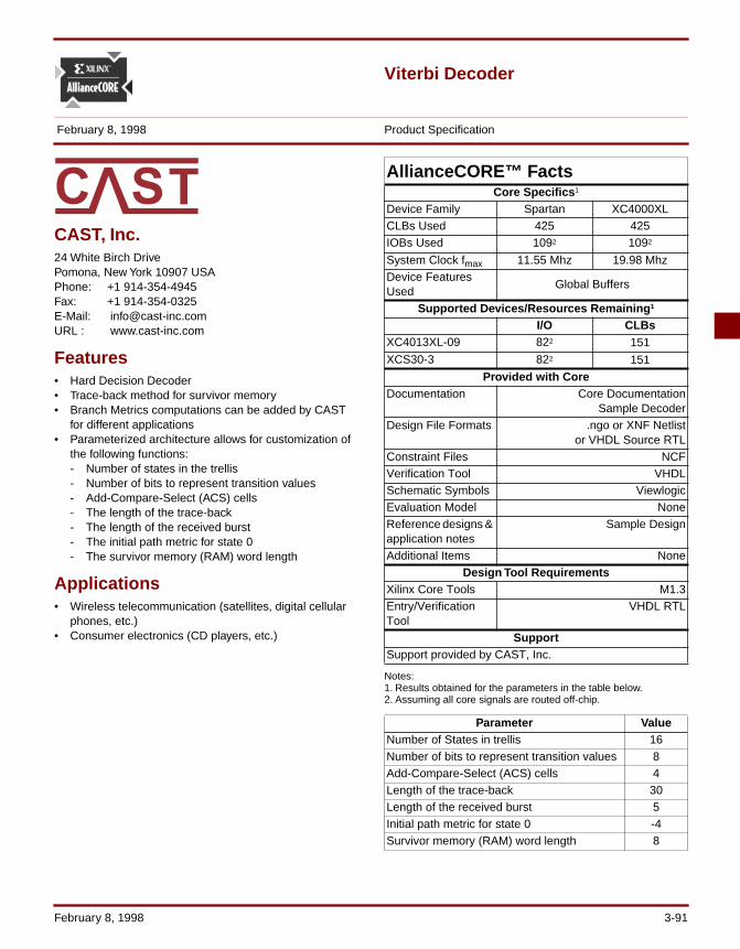
Viterbi Decoder
February 8, 1998 Product Specification
CAST, Inc.24 White Birch DrivePomona, New York 10907 USAPhone: +1 914-354-4945Fax: +1 914-354-0325E-Mail: [email protected] : www.cast-inc.com
Features• Hard Decision Decoder• Trace-back method for survivor memory• Branch Metrics computations can be added by CAST
for different applications• Parameterized architecture allows for customization of
the following functions:- Number of states in the trellis- Number of bits to represent transition values- Add-Compare-Select (ACS) cells- The length of the trace-back- The length of the received burst- The initial path metric for state 0- The survivor memory (RAM) word length
Applications• Wireless telecommunication (satellites, digital cellular
phones, etc.)• Consumer electronics (CD players, etc.)
Notes:1. Results obtained for the parameters in the table below.2. Assuming all core signals are routed off-chip.
AllianceCORE™ FactsCore Specifics 1
Device Family Spartan XC4000XLCLBs Used 425 425IOBs Used 1092 1092
System Clock fmax 11.55 Mhz 19.98 MhzDevice Features Used
Global Buffers
Supported Devices/Resources Remaining 1
I/O CLBsXC4013XL-09 822 151
XCS30-3 822 151
Provided with CoreDocumentation Core Documentation
Sample DecoderDesign File Formats .ngo or XNF Netlist
or VHDL Source RTLConstraint Files NCFVerification Tool VHDLSchematic Symbols ViewlogicEvaluation Model NoneReference designs & application notes
Sample Design
Additional Items NoneDesign Tool Requirements
Xilinx Core Tools M1.3Entry/Verification Tool
VHDL RTL
SupportSupport provided by CAST, Inc.
Parameter ValueNumber of States in trellis 16Number of bits to represent transition values 8Add-Compare-Select (ACS) cells 4Length of the trace-back 30Length of the received burst 5Initial path metric for state 0 -4Survivor memory (RAM) word length 8
February 8, 1998 3-91
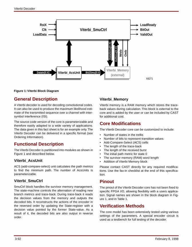
Viterbi Decoder
General DescriptionA Viterbi decoder is used for decoding convolutional codes.It can also be used to produce the maximum likelihood esti-mate of the transmitted sequence over a channel with inter-symbol interference (ISI).
The source code version of the core is parameterizable andtherefore easily adapted to a wide variety of applications.The data given in this fact sheet is for an example only. TheViterbi Decoder can be delivered in a specific format (seeOrdering Information).
Functional DescriptionThe Viterbi Decoder is partitioned into modules as shown inFigure 1 and described below.
Viterbi_AcsUnitACS (add-compare-select) unit calculates the path metricsto find the minimum path. The number of AcsUnits isparameterizable.
Viterbi_SmuCtrlSmuCtrl block handles the survivor memory management.The state-machine controls the alternation of reading newbranch metrics and trace-back. During trace-back it readsthe decision values from the memory and outputs thedecoded bits. It reconstructs the actions of the encoder inthe reversed order by updating the State-register with adecision value pointed by the former State-value. As aresult of it, the decoded bits are also output in reverseorder.
Viterbi_MemoryViterbi memory is a RAM memory which stores the trace-back values during calculation. This block is external to thecore and is added by the user or can be included by CASTfor additional cost.
Core ModificationsThe Viterbi Decoder core can be customized to include:
• Number of states in the trellis• Number of bits to represent transition values• Add-Compare-Select (ACS) cells• The length of the trace-back• The length of the received burst• The initial path metric for state 0• The survivor memory (RAM) word length• Addition of Viterbi Memory block
Please contact CAST directly for any required modifica-tions. Use the fax-in checklist at the end of this specifica-tion.
PinoutThe pinout of the Viterbi Decoder core has not been fixed tospecific FPGA I/O, allowing flexibility with a users applica-tion. Signal names are shown in the block diagram in Fig-ure 1, and in Table 1.
Verification MethodsThe core model has been extensively tested using varioussettings of the parameters. A special encoder circuit isused as a testbench for full testing of the decoder.
Ad
Sm
u[0
:X]
Da
taS
mu
[0:X
]
DataIn[0:X] Bit2Smu[0:X]Viterbi_AcsUnitViterbi_Memory
(external)
LoadReadyBitOutValidOut
RstXClk
LoadDataViterbi_SmuCtrl
We
b
Oe
b
X8271
Figure 1: Viterbi Block Diagram
3-92 February 8, 1998
Cast Inc.
Table 1: Core Signal Pinout
Recommended Design ExperienceThe user must be familiar with HDL design methodology aswell as instantiation of Xilinx netlists in a hierarchical designenvironment.
Ordering InformationThe Viterbi Decoder is available for purchase directly fromCAST, Inc. If the XNF Netlist format is required, a setting forthe parameters will have to submitted before the netlist canbe created. Ask CAST, Inc. for details.
Related InformationA.B. Carlson, Communications systems, McGraw-Hill,1986.
E.A. Lee, D.G. Messerschmitt, Digital Communication,Boston, MA Kluwer Academic Publishers, 1988.
G.D. Forney, Jr., “The Viterbi algorithm:, Proc. IEEE, vol.61, pp.268-277, March 1973.
G. Fettweis, H. Meyr, “High-Speed Parallel Decoding: Algo-rithm and VLSI-Architecture”, IEEE Comm. Magazine, pp.46-55, May 1991.
G. Feygin, P.G.Gulak, “Architectural Tradeoffs for SurvivorSequence Memory Management in Viterbi decoders”,IEEE Trans. Commun. Tech., vol. 41, no. 3, March 1993.
R. Cypher, C.B.Shung, “Generalized Trace-Back tech-niques for Survivor Memory Management in the ViterbiAlgorithm”, Journal of VLSI Signal Processing, 5, 85-94(1993).
Motorola, “Convolutional Encoding and Viterbi DecodingUsing the DSP56001 with a V.32 Modem Trellis Example,Motorola Inc. 1989.
B. Sklar, “Digital Communications, fundamentals and applications”, Prentice Hall International Inc. 1988.
Xilinx Programmable LogicFor information on Xilinx programmable logic or develop-ment system software, contact your local Xilinx sales office,or:
Xilinx, Inc.2100 Logic DriveSan Jose, CA 95124Phone: +1 408-559-7778Fax: +1 408-559-7114URL: www.xilinx.com
For general Xilinx literature, contact:
Phone: +1 800-231-3386 (inside the US)+1 408-879-5017 (outside the US)
E-mail: [email protected]
For AllianceCORE™ specific information, contact:
Phone: +1 408-879-5381E-mail: [email protected]: www.xilinx.com/products/logicore/alliance/
tblpart.htm
SignalSignal
DirectionDescription
Input Interface SignalsRstX Input Asynchronous reset, active
lowClk Input Common ClockLoadData Input Enables Data LoadingDataIn[0:X] Input Transition values input, the
width depends on the num-ber of ACS-units
Output Interface SignalsLoadReady Output Indicates Ready for DataBitOut Output Decoded Output BitValidOut Output Indicates the Valid Output
DataExternal Memory Interface SignalsBits2Smu[0:X] Output Output data to external Mem-
oryDataSmu[0:X] Input Input data from external
MemoryWeb Output Write Enable to external
MemoryOeb Output Read Enable to external
MemoryAdSmu[0:X] Output Address to external Memory
February 8, 1998 3-93

Viterbi Decoder
To: CAST, Inc.FAX: +1 914-354-0325E-mail: [email protected]
From:
Company:
Name:
Address:
Country:
Phone:
Fax:
E-mail:
CAST, Inc. will customize and deliver a Xilinx optimizednetlist for the specific Viterbi Decoder implementation yourequire. Please fill out and fax or email this information toCAST so they can provide you with an accurate responseto, and quote for your requirements.
Implementation Issues
1. Number of states in trellis: ______
2. Number of bits to represent transition values: ______
3. Add-compare-select cells: ______
4. Length of trace-back: ______
5. Length of receiveR burst:______
6. Initial path metric for state 0: ______
7. Survivor memory word length: ______
Business Issues
8. Indicate timescales of requirement:a. date for decision ______b. date for placing order ______c. required delivery date ______
9. Indicate your area of responsibility:______ decision maker______ budget holder______ recommender
10. Has a budget been allocated for the purchase?Yes ______ No ______
11. What volume do you expect to ship of the product thatwill use this core? ______
12. What major factors will influence your decision?______ cost______ customization______ testing______ implementation size
13. Are you considering any other solutions?
Viterbi Implementation Request Form
3-94 February 8, 1998

Processor Products Table of Contents
February 8, 1998
TX400 Series RISC CPU Cores . . . . . . . . . . . . . . . . . . . . . . . . . . . . . . . . . . . . . . .3-97RISC CPU Core Design Base Board . . . . . . . . . . . . . . . . . . . . . . . . . . . . . . . . . .3-103Scalable Development Platform Integrated Software . . . . . . . . . . . . . . . . . . . . .3-107V8-uRISC 8-bit RISC Microprocessor . . . . . . . . . . . . . . . . . . . . . . . . . . . . . . . . .3-109IntelliCoreTM Prototyping System . . . . . . . . . . . . . . . . . . . . . . . . . . . . . . . . . . . . . 3-115
February 8, 1998 3-95

Processor Products Table of Contents
3-96 February 8, 1998

TX400 Series RISC CPU Cores
December 15, 1997 Product Specification
T7L Technology, Inc.220 Duncanmill RoadSuite 307North York, OntarioCanada, M3B 3J5Phone: +1 416-445-4783Fax: +1 416-445-5741E-mail: [email protected]: www.t7l.com
Features• Scalable RISC CPU cores for embedded controller
applications• Compact RISC-oriented opcode design makes the core
very small and requires less program size• 26 different configurations, depending on application
requirements- 8 - 32 bit data width- 8 - 32 bit data address width- 10 - 24 bit instruction length- 10 - 24 bit program address width- 1K - 16M bit maximum program size
• Function generator based logic structure and fully optimized for Xilinx FPGA physical architecture
• Up to 33Mhz operation • Three stage, fully-balanced pipeline machine for
prefetch/branch, instruction decode and execution• Built-in hardware stack unit for instant program
switching and low latency interrupt dispatching• Debug version with snoop capability provided with each
production core• Ships with integrated development toolkit for CPU core
embedding and run-time debugging- Support for high-level programming languages- Symbolic Assembler/Debugger- C Compiler
Applications• Microcontroller Unit (MCU)• Real-time Digital Signal Processor• Dedicated Communication Processor• Integrated Embedded System• Programmable Peripheral Controller
AllianceCORE ™ FactsCore Specifics
Device Family XC4000E, EX, XLCLBs Used
See Table 1IOBs UsedSystem clock fmaxDevice Features Used Select RAM
Supported Devices/Resources Remaining
See Table 1
Provided with Core
Documentation Design ManualH/W & S/W, Compiler,
Assembly & CDesign File Formats EDIF, .xnf, .ngo netlistsConstraint Files N/AVerification Tool Development SoftwareSchematic Symbols FoundationEvaluation Model Design base boardReference designs & application notes
Music Panel sample design inVHDL and Schematics
Additional Items PC Windows-based Debugger,assembly compiler and vector
generator;Debug Version of core
Design Tool Requirements
Xilinx Core Tools Alliance/Foundation 1.3Entry/Verification Tool
VHDL or Schematic
Support
Support provided by T7L Technology, Inc.
December 15, 1997 3-97
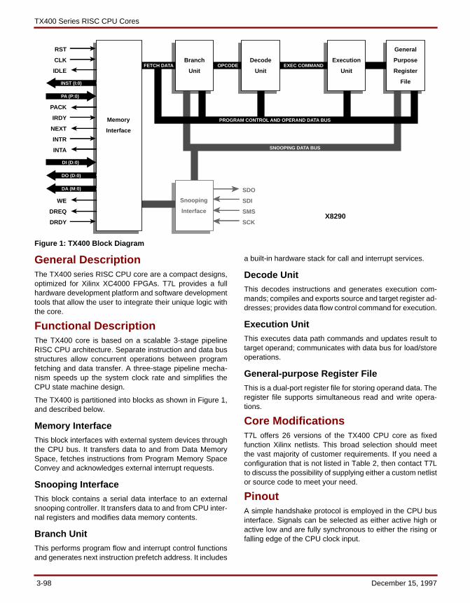
TX400 Series RISC CPU Cores
General DescriptionThe TX400 series RISC CPU core are a compact designs,optimized for Xilinx XC4000 FPGAs. T7L provides a fullhardware development platform and software developmenttools that allow the user to integrate their unique logic withthe core.
Functional DescriptionThe TX400 core is based on a scalable 3-stage pipelineRISC CPU architecture. Separate instruction and data busstructures allow concurrent operations between programfetching and data transfer. A three-stage pipeline mecha-nism speeds up the system clock rate and simplifies theCPU state machine design.
The TX400 is partitioned into blocks as shown in Figure 1,and described below.
Memory InterfaceThis block interfaces with external system devices throughthe CPU bus. It transfers data to and from Data MemorySpace, fetches instructions from Program Memory SpaceConvey and acknowledges external interrupt requests.
Snooping InterfaceThis block contains a serial data interface to an externalsnooping controller. It transfers data to and from CPU inter-nal registers and modifies data memory contents.
Branch UnitThis performs program flow and interrupt control functionsand generates next instruction prefetch address. It includes
a built-in hardware stack for call and interrupt services.
Decode UnitThis decodes instructions and generates execution com-mands; compiles and exports source and target register ad-dresses; provides data flow control command for execution.
Execution UnitThis executes data path commands and updates result totarget operand; communicates with data bus for load/storeoperations.
General-purpose Register FileThis is a dual-port register file for storing operand data. Theregister file supports simultaneous read and write opera-tions.
Core ModificationsT7L offers 26 versions of the TX400 CPU core as fixedfunction Xilinx netlists. This broad selection should meetthe vast majority of customer requirements. If you need aconfiguration that is not listed in Table 2, then contact T7Lto discuss the possibility of supplying either a custom netlistor source code to meet your need.
PinoutA simple handshake protocol is employed in the CPU businterface. Signals can be selected as either active high oractive low and are fully synchronous to either the rising orfalling edge of the CPU clock input.
SDO
SDI
SMS
SCK
Branch
Unit
Decode
Unit
Execution
Unit
General
Purpose
Register
File
FETCH DATA OPCODE EXEC COMMAND
PROGRAM CONTROL AND OPERAND DATA BUS
SNOOPING DATA BUS
RST
CLK
IDLE
PACK
IRDY
NEXT
INTR
INTA
WE
DREQ
DRDY
PA (P:0)
INST (I:0)
DI (D:0)
DO (D:0)
DA (M:0)
Memory
Interface
Snooping
InterfaceX8290
Figure 1: TX400 Block Diagram
3-98 December 15, 1997
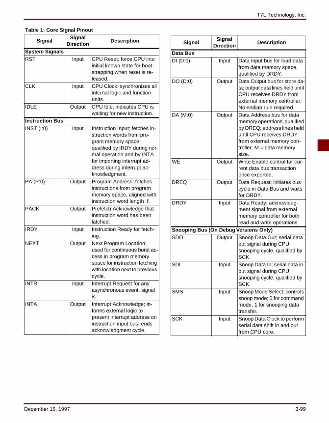
T7L Technology, Inc.
Table 1: Core Signal Pinout
SignalSignal
DirectionDescription
System SignalsRST Input CPU Reset; force CPU into
initial known state for boot-strapping when reset is re-leased.
CLK Input CPU Clock; synchronizes all internal logic and function units.
IDLE Output CPU Idle; indicates CPU is waiting for new instruction.
Instruction BusINST (I:0) Input Instruction Input; fetches in-
struction words from pro-gram memory space, qualified by IRDY during nor-mal operation and by INTA for importing interrupt ad-dress during interrupt ac-knowledgment.
PA (P:0) Output Program Address; fetches instructions from program memory space, aligned with instruction word length ‘I’.
PACK Output Prefetch Acknowledge that instruction word has been latched.
IRDY Input Instruction Ready for fetch-ing.
NEXT Output Next Program Location; used for continuous burst ac-cess in program memory space for instruction fetching with location next to previous cycle.
INTR Input Interrupt Request for any asynchronous event. signal is.
INTA Output Interrupt Acknowledge; in-forms external logic to present interrupt address on instruction input bus; ends acknowledgment cycle.
SignalSignal
DirectionDescription
Data BusDI (D:0) Input Data Input bus for load data
from data memory space, qualified by DRDY.
DO (D:0) Output Data Output bus for store da-ta; output data lines held until CPU receives DRDY from external memory controller. No endian rule required.
DA (M:0) Output Data Address bus for data memory operations, qualified by DREQ; address lines held until CPU receives DRDY from external memory con-troller. M = data memory size.
WE Output Write Enable control for cur-rent data bus transaction once exported.
DREQ Output Data Request; initiates bus cycle in Data Bus and waits for DRDY.
DRDY Input Data Ready; acknowledg-ment signal from external memory controller for both read and write operations.
Snooping Bus (On Debug Versions Only)SDO Output Snoop Data Out; serial data
out signal during CPU snooping cycle, qualified by SCK.
SDI Input Snoop Data In; serial data in-put signal during CPU snooping cycle, qualified by SCK.
SMS Input Snoop Mode Select; controls snoop mode; 0 for command mode, 1 for snooping data transfer.
SCK Input Snoop Data Clock to perform serial data shift in and out from CPU core.
December 15, 1997 3-99
TX400 Series RISC CPU Cores
There are four groups of signals (All scalable variablesarezero basis).• System Signals - for overall CPU control and status
information• Instruction Bus - for fetching instruction words from
Program Memory Space• Data Bus - for load or store of data into Data Memory &
IO Space as requested by program
Snooping Bus - signals for reading or modifying CPU inter-nal registers and data memory contents. These signals areon the debug versions of the cores only.
The pinout is not fixed to any specific device I/O. Signalnames are provided in the block diagram shown in Figure1, and described in Table 1.
Verification MethodsTest vectors generated by the V-System V4.4J from ModelTechnology have been used to test every instruction, in-struction combination and interrupt event for these cores.They have also been silicon proven in Xilinx XC4000 FP-GAs using the T7L Design Base Board, which is availableseparately from T7L.
Selecting the Right CoreThere are 26 pre-implemented versions of the TX400, di-vided into seven groups. The characteristics of each areshown in Table 2. Each version is purchased and shippedseparately. Each core comes with Xilinx netlists for a debugversion that includes snooping circuitry and I/O, and a pro-duction version without snoop capability. The implementa-tion statistics shown in Table 3 are for the productionversion of each core.
• Group 1 TX401 - Microcontroller type CPU cores for embedded applications, and requires a small instruction set. Sizes range from 8 to 10-bit data and 10 to 12-bit instruction length.
• Group 2 TX402 - Standard RISC CPU cores for embedded controller applications. Its size ranges from 8 to 10-bit data and 12 to 16-bit instruction length.
• Group 3 TX403 - Compact RISC CPU cores for embedded system applications and requires a small instruction set. Its size ranges from 12 to 16-bit data and 12 to 16-bit instruction length.
• Group 4 TX404 - Mid-size RISC CPU cores for embedded system applications. Its size ranges from 12 to 16-bit data and 12 to 16-bit instruction length.
• Group 5 TX405 - Mid-size RISC CPU cores for DSP system applications. Its size ranges from 12 to 16-bit data and 12 to 16-bit instruction length.
• Group 6 TX406 - Powerful RISC CPU cores for embedded system applications. Its size ranges from 24 to 32-bit data and 16 to 24-bit instruction length.
• Group 7 TX407 - Powerful RISC CPU cores for DSP system applications. Its size ranges from 24 to 32-bit data and 16 to 24-bit instruction length.
Recommended Design ExperienceTo integrate a TX-400 core in an embedded system with aXilinx XC4000 FPGA requires a simple design flow. Thecore is supplied in the form of Xilinx .ngo, EDIF, .xnf netlistsand schematic symbol. Users include the core by eithercapturing into the top-level schematic or declaring/instanti-ating as a component in the top-level VHDL model.
Users should be familiar with RISC processors, processorcode development environments and embedded systemdesign.
Available Support ProductsT7L offers 26 versions of the TX400 RISC CPU core alongwith hardware tools for integrating them into Xilinx FPGAs.T7L also supplies a complete software development envi-ronment. Products include:• SDP Design Base Board (with Xilinx XC4000 FPGA) -
$295• Windows95 based assembler, debugger, monitor and
vector generator (provided with core)• C-Compiler (provided with core)
Ordering InformationThere are 26 different cores in the TX400 family. Specifica-tions for each are detailed in Table 2. Each comes with Xil-inx netlists for production and debug versions. VHDLsource is available for additional cost. For more informationon these or other T7L products, contact T7L Technology di-rectly.
Related Information
Xilinx Programmable LogicFor information on Xilinx programmable logic or develop-ment system software, contact your local Xilinx sales office,or:
Xilinx, Inc.2100 Logic DriveSan Jose, CA 95124Phone: +1 408-559-7778Fax: +1 408-559-7114URL: www.xilinx.com
For general Xilinx literature, contact:Phone: +1 800-231-3386 (inside the US)
+1 408-879-5017 (outside the US)E-mail: [email protected]
For AllianceCORE™ specific information, contact:Phone: +1 408-879-5381E-mail: [email protected]: www.xilinx.com/products/logicore/alliance/
tblpart.htm
3-100 December 15, 1997
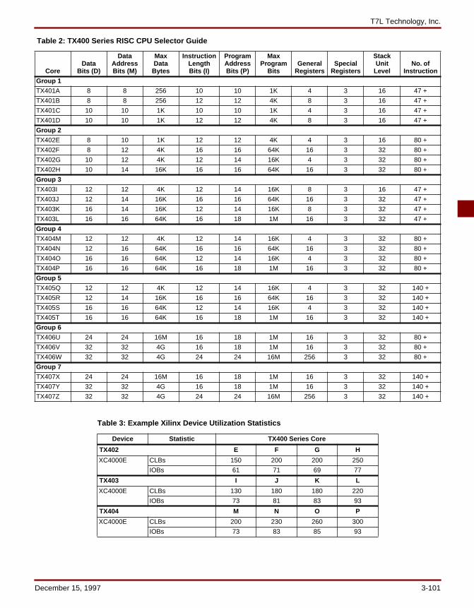
T7L Technology, Inc.
Table 2: TX400 Series RISC CPU Selector Guide
CoreData
Bits (D)
DataAddressBits (M)
MaxData
Bytes
Instruction LengthBits (I)
ProgramAddressBits (P)
MaxProgram
BitsGeneral
RegistersSpecial
Registers
StackUnit
LevelNo. of
Instruction
Group 1
TX401A 8 8 256 10 10 1K 4 3 16 47 +
TX401B 8 8 256 12 12 4K 8 3 16 47 +
TX401C 10 10 1K 10 10 1K 4 3 16 47 +
TX401D 10 10 1K 12 12 4K 8 3 16 47 +
Group 2
TX402E 8 10 1K 12 12 4K 4 3 16 80 +
TX402F 8 12 4K 16 16 64K 16 3 32 80 +
TX402G 10 12 4K 12 14 16K 4 3 32 80 +
TX402H 10 14 16K 16 16 64K 16 3 32 80 +
Group 3
TX403I 12 12 4K 12 14 16K 8 3 16 47 +
TX403J 12 14 16K 16 16 64K 16 3 32 47 +
TX403K 16 14 16K 12 14 16K 8 3 32 47 +
TX403L 16 16 64K 16 18 1M 16 3 32 47 +
Group 4
TX404M 12 12 4K 12 14 16K 4 3 32 80 +
TX404N 12 16 64K 16 16 64K 16 3 32 80 +
TX404O 16 16 64K 12 14 16K 4 3 32 80 +
TX404P 16 16 64K 16 18 1M 16 3 32 80 +
Group 5
TX405Q 12 12 4K 12 14 16K 4 3 32 140 +
TX405R 12 14 16K 16 16 64K 16 3 32 140 +
TX405S 16 16 64K 12 14 16K 4 3 32 140 +
TX405T 16 16 64K 16 18 1M 16 3 32 140 +
Group 6
TX406U 24 24 16M 16 18 1M 16 3 32 80 +
TX406V 32 32 4G 16 18 1M 16 3 32 80 +
TX406W 32 32 4G 24 24 16M 256 3 32 80 +
Group 7
TX407X 24 24 16M 16 18 1M 16 3 32 140 +
TX407Y 32 32 4G 16 18 1M 16 3 32 140 +
TX407Z 32 32 4G 24 24 16M 256 3 32 140 +
Table 3: Example Xilinx Device Utilization Statistics
Device Statistic TX400 Series Core
TX402 E F G H
XC4000E CLBs 150 200 200 250
IOBs 61 71 69 77
TX403 I J K L
XC4000E CLBs 130 180 180 220
IOBs 73 81 83 93
TX404 M N O P
XC4000E CLBs 200 230 260 300
IOBs 73 83 85 93
December 15, 1997 3-101

TX400 Series RISC CPU Cores
3-102 December 15, 1997
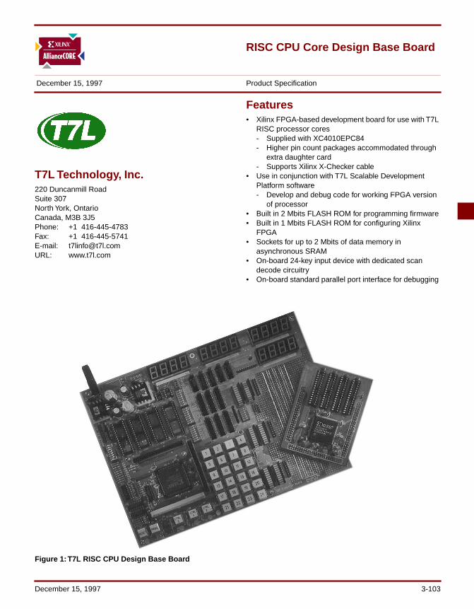
RISC CPU Core Design Base Board
December 15, 1997 Product Specification
T7L Technology, Inc.220 Duncanmill RoadSuite 307North York, OntarioCanada, M3B 3J5Phone: +1 416-445-4783Fax: +1 416-445-5741E-mail: [email protected]: www.t7l.com
Features• Xilinx FPGA-based development board for use with T7L
RISC processor cores- Supplied with XC4010EPC84- Higher pin count packages accommodated through
extra daughter card- Supports Xilinx X-Checker cable
• Use in conjunction with T7L Scalable Development Platform software- Develop and debug code for working FPGA version
of processor• Built in 2 Mbits FLASH ROM for programming firmware• Built in 1 Mbits FLASH ROM for configuring Xilinx
FPGA• Sockets for up to 2 Mbits of data memory in
asynchronous SRAM• On-board 24-key input device with dedicated scan
decode circuitry• On-board standard parallel port interface for debugging
Figure 1: T7L RISC CPU Design Base Board
December 15, 1997 3-103

RISC CPU Core Design Base Board
and downloading• 48 user definable, general purpose I/O lines with 48
individual status LEDs• 16 seven-segment LED display with dedicated decode
circuitry
General DescriptionThe T7L Scalable Development Platform (SDP) designbase board is offered as part of the design kit for buildingprototypes of embedded systems using TX400 RISC CPUcores. It comes with a Xilinx XC4010EPC84 chip and somebasic I/O devices.
The user is only required to glue together the CPU core, onboard peripherals and application-specific I/O logic througheither schematic capture or by creating a top-level VHDLmodel. With help of Xilinx place-and-route software, thesystem will then quickly be converted into physical configu-ration bitstream. Once the data file is downloaded into theon-board FPGA, the development board becomes a hard-ware prototype of the system running at speed for real-timesoftware development, evaluation and debug.
Functional DescriptionThe RISC CPU Core Design Base Board contains every-thing you need to develop and debug a RISC processorbased FPGA design.
FPGA ChipBasic on-board FPGA device is an XC4000E chip in aPLCC-84 package, upgradable to any XC4000E/EX/XLdevice in larger packages by means of a daughter board.Configuration data is downloaded from a PC system viastandard parallel port.
Program MemoryThere are two Flash ROMs for user’s firmware program andinitial data items. It supports 2 Mbits of program memoryspace. On-board programming utility for firmware codes isprovided in the T7L SDP software tools.
Data MemoryThere are two IC sockets for program data in asynchronousSRAM. It supports up to 1 Mbits of data memory space.Each IC socket is for any 32-pin DIP package static mem-ory device, such 61 series fast SRAM devices.
Configuration MemoryThere is one Flash ROM for user’s Xilinx FPGA configura-tion. It supports 1 Mbits of FPGA configuration data,upgradable for 2 Mbits. On-board programming utility forFPGA configuration bit image is provided in the T7L SDPsoftware tools.
Control KeysThere are seven input keys designed for control functions:
• Reset: User-defined reset input for FPGA and/or on board devices
• Program: To initialize the FPGA and wait for re-load of configuration data
• Init: To hold the FPGA and wait for re-load of configuration data via JTAG port.
• User Control: Four user-defined control input keys with external latching functions.
Keypad MatrixA 24-key input device is provided on board. It is organizedin a 3 x 8 matrix array. Scan decoding is supported exter-nally by a TTL chip that saves a lot of I/O pins to the FPGAdevice.
LED DisplayTotal 16 seven-segment LED display units on board. Theyare time multiplexed and shared data lines. It is supportedby an external TTL decoder in order to save I/O pins to andfrom an FPGA device.
User I/O PortsThere are 48 general-purpose I/O lines for user-definedlogic functions, grouped into three 16-bit I/O ports. Thesecan be connected to off-board peripheral device usingcables. Each I/O line is supported by a status LED for realtime logic debugging.
Download PortAn interface is provided to download configuration data andperform JTAG boundary scan testing. It supports the XilinxX-Checker cable and software utility.
Parallel PortAn on-board 25-pin connector is built for CPU real-timehardware debugging, configuration data downloading andJTAG boundary scan testing. Hardware debug facilities forT7L CPU core is provided in the T7L SDP software tools.
Available Support ProductsT7L also offers 26 versions of the TX400 RISC CPU corealong with a development software. When used with thedesign base board, the customer has a complete develop-ment environment for integrating and testing T7L RISCcores in Xilinx FPGAs.
Ordering InformationThe Design Base Board lists for $295 directly from T7LTechnology. For more information on this or associatedproducts, contact T7L directly.
3-104 December 15, 1997
T7l Technology, Inc.
Related InformationXilinx Programmable LogicFor information on Xilinx programmable logic or develop-ment system software, contact your local Xilinx sales office,or:
Xilinx, Inc.2100 Logic DriveSan Jose, CA 95124Phone: +1 408-559-7778Fax: +1 408-559-7114URL: www.xilinx.com
For general Xilinx literature, contact:
Phone: +1 800-231-3386 (inside the US)+1 408-879-5017 (outside the US)
E-mail: [email protected]
For AllianceCORE™ specific information, contact:
Phone: +1 408-879-5381E-mail: [email protected]: www.xilinx.com/products/logicore/alliance/
tblpart.htm
December 15, 1997 3-105

RISC CPU Core Design Base Board
3-106 December 15, 1997
Scalable Development Platform Integrated Software
December 15, 1997 Product Specification
T7L Technology, Inc.220 Duncanmill RoadSuite 307North York, OntarioCanada, M3B 3J5Phone: +1 416-445-4783Fax: +1 416-445-5741E-mail: [email protected]: www.t7l.com
Features• Software development platform for T7L RISC CPU
cores- Supplied free with CPU core license
• Complete integrated software tool set- Project manager- Source code editor- C compiler - Assembler- Object file linker- Test vector generator- Software debugger- Hardware debugger
• Runs under Windows 95
General DescriptionThe T7L Scalable Development Platform (T7L SDP) is asoftware development platform for T7L Scalable CPU prod-ucts and is free for all T7L CPU core license users. It pro-vides project management, source code editor, C compiler,assembler, object file linker, test vector generator and facil-ities to help in the program debugging process during soft-
Figure 1: SDP Integrated Software Debugger Screen
December 15, 1997 3-107
Scalable Development Platform Integrated Software
ware and hardware development. SDP is designed to rununder Windows 95 or upward compatibles. It does not workfor Windows 3.1 or older versions.
Functional DescriptionThe T7L SDP toolkit includes a complete set of softwaretools as described below.
Project ManagerIt provides a GUI based project development environmentfor use in embedding T7L CPU core and in software pro-gramming. Various file house-keeping functions are sup-ported for user’s design data base.
Source Code EditorThis is a built-in text editor for source code and test vectorediting. It provides an integrated design entry tool on thesame development platform.
C CompilerA C Compiler is provided for high-level language softwareprogramming. It is an embedded version of standard C lan-guage processor and generates assembly source code forfurther optimization.
AssemblerThis is a super symbolic assembler for object code genera-tion according to the user’s target CPU configuration. Theuser can modify mnemonic and operand syntax strings asrequired. A new style of assembly programming was cre-ated to cope with the T7L CPU scalability.
Object File LinkerThis helps the user to combine object codes and commonlibrary elements together and generates system firmwarecodes.
Test Vector GeneratorThis generates an input stimulus file in ASCII form for sys-tem simulation. The file can be merged with the user’s sys-tem test vectors for chip level testing. The vectors alsosupport memory file format (.mem) for Xilinx LogiBLOXRAM/ROM generator. With the Test Vector Generator, T7LSDP is perfectly integrated with Xilinx place and route toolsin internal ROM-base program development.
Software DebuggerThis is a virtual CPU simulator for the T7L scalable RISCprocessor. Software debugging can be carried out in paral-lel with the target hardware prototype. It supports debug-ging commands, Restart, Stop, Go, Step, Set Break andClear Break, and displays all register and data memorycontents.
Hardware DebuggerA hardware debugging tool is supplied for real time at-speed debugging. Using a standard parallel interface, thedebugger can remotely read and modify internal CPU reg-ister and data memory contents in the target hardware sys-tem. Other than software debugging commands, thedebugger also supports Xilinx FPGA configuration datadownloading. A T7L SDP snooping bus port is defined fordebugging during technical development and for on-sitetroubleshooting. An optional T7L SDP debugger cable isprovided for on-site re-configuring and debugging.
Available Support ProductsT7L offers 26 versions of the TX400 RISC CPU core eachbundled with the SDP Integrated Software. When used withthe SDP Design Base Board, customers have a completedevelopment environment for integrating and testing T7LRISC cores in Xilinx FPGAs.
The software manual and all other documentation can bedownloaded from the T7L web site at www.t7l.com.
Ordering InformationThe SDP Integrated Software is bundled free with all T7LRISC CPU cores. For more information on this or associ-ated products, contact T7L directly.
Related InformationXilinx Programmable LogicFor information on Xilinx programmable logic or develop-ment system software, contact your local Xilinx sales office,or:
Xilinx, Inc.2100 Logic DriveSan Jose, CA 95124Phone: +1 408-559-7778Fax: +1 408-559-7114URL: www.xilinx.com
For general Xilinx literature, contact:
Phone: +1 800-231-3386 (inside the US)+1 408-879-5017 (outside the US)
E-mail: [email protected]
For AllianceCORE™ specific information, contact:
Phone: +1 408-879-5381E-mail: [email protected]: www.xilinx.com/products/logicore/alliance/
tblpart.htm
3-108 December 15, 1997
V8-uRISC 8-bit RISC Microprocessor
February 8, 1998 Product Specification
VAutomation, Inc.20 Trafalgar SquareNashua, NH 03063Phone: +1 603-882-2282Fax: +1 603-882-1587E-mail: [email protected]: www.vautomation.com
Features• RISC architecture for low gate count and high
performance • Single Cycle instruction execution for all register to
register opcodes • High Code density, many opcodes are a single byte • 33 opcodes, 4 addressing modes, 2 user defined
opcodes • 8-bit ALU • 64K byte addressing capability • Two banks of 8-bit general purpose registers • 16-bit program counter and stack pointer • Seven maskable interrupts, one non-maskable • Assembler, debugger and simulator available now, C
Compiler (May ’98)• IntelliCoreTM Prototyping System available for
evaluation and rapid product development• Includes VHDL/Verilog source code for the following
peripherals:- UART- DMA controller- I2C EEPROM interface- P1284 parallel interface- Page register
Notes:1. Assuming all core signals are routed off-chip.2. For CPU and register file only. Figures do not include
peripherals.
AllianceCORE™ FactsCore Specifics 2
Device Family XC4000EMacrocells Used 268IOBs Used 541
CLKIOBs Used 1System Clock fmax 15.9 MHzDevice Features Used SelectRAM
Supported Devices/Resources Remaining 2
I/O CLBsXC4013E-1 PQ160 741 308
Provided with CoreDocumentation Reference ManualDesign File Formats XNF, EDIF, VHDL or Verilog netlistConstraint Files Example .ucfVerification Tool Test BenchSchematic Symbols NoneEvaluation Model NoneReference designs & application notes
Includes VHDL/Verilog source forUART, DMA controller, I2C EE-
PROM I/F, P1284 I/F, page registerAdditional Items IntelliCore™ Prototype system
available extraDesign Tool Requirements
Xilinx Core Tools Alliance 1.3Entry/Verification Tool
FPGA Synthesis tool required forsupplied peripherals;
Model Tech for simulationSupport
Support provided by VAutomation.
February 8, 1998 3-109
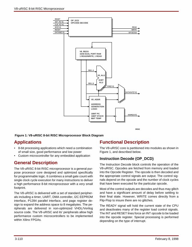
V8-uRISC 8-bit RISC Microprocessor
Applications• 8-bit processing applications which need a combination
of small size, good performance and low power• Custom microcontroller for any embedded application
General DescriptionThe V8-uRISC 8-bit RISC microprocessor is a general pur-pose processor core designed and optimized specificallyfor programmable logic. It combines a small gate count withsingle clock cycle execution for many instructions to delivera high performance 8-bit microprocessor with a very smallfootprint.
The V8-uRISC is delivered with a set of standard peripher-als including a timer, UART, DMA controller, I2C EEPROMinterface, P1284 parallel interface, and page register de-sign to expand the address space to 8 megabytes. The pe-ripherals are delivered in non-optimized VHDL/Verilogsource code. The V8-uRISC and its’ peripherals allow highperformance custom microcontrollers to be implementedwithin Xilinx FPGAs.
Functional DescriptionThe V8-uRISC core is partitioned into modules as shown inFigure 1, and described below.
Instruction Decode (OP_DCD)The Instruction Decode block controls the operation of theV8-uRISC. Opcodes are fetched from memory and loadedinto the Opcode Register. The opcode is then decoded andthe appropriate control signals are output. The control sig-nals depend on the opcode and the number of clock cyclesthat have been executed for the particular opcode.
Most of the control outputs are decodes and thus may glitchand have a significant amount of delay before settling totheir final state. However, WRITE comes directly from aFlip-Flop to insure there are no glitches.
The READY signal will hold the current state of the CPUand deactivates many of the register load control signals.The INT and RESET lines force an INT opcode to be loadedinto the opcode register. Special processing is performeddepending on the type of interrupt.
Figure 1: V8-uRISC 8-bit RISC Microprocessor Block Diagram
X8342
V8_REGS16X8 DUAL PORT RAM1 READ/WRITE, 1 READ
V8_ADDR
ADDRESSGENERATIONLOGIC
16BIT PC16BIT STACK8BIT TEMP
OP_DCDOPCODE DECODE
READ
WRITE
OP FETCH
DATAOUT[7:0]
ADDR[15:0]
REG_A
REG_B
PSR[7:0]
RESET
SET_P[7:4]
CLR_P[7:4]
INT[7:0]
READY
DATAIN[7:0]
V8_ALU
8-BITALU
3-110 February 8, 1998

VAutomation, Inc.
Arithmetic Logic Unit (V8_ALU)The ALU block performs the 8 bit arithmetic and logical op-erations. The inputs to the ALU come directly from the Reg-ister File or from the TEMP register in the V8-uRISC_ADDRmodule. Certain constants such as 0 and 1 can also be se-lected as inputs to the ALU for increment and decrementoperations.
The ALU includes bit-manipulation logic to allow testing,setting and clearing of a single bit of a byte. This is a com-mon function in embedded microcontrollers.
The Processor Status Register (PSR) shown in Table 1, isalso located within the V8_ALU block. Most opcodes passdata through the ALU so that the appropriate PSR flags canbe updated. A logic 1 on the SET_P signals will cause thecorresponding bit in the PSR register to be set; a logic 1 onthe CLR_P pin will clear the corresponding PSR bit to zero.These signals are typically connected to IO device statuslines that allow the V8-uRISC to quickly test and branch onthese bits.
Table 1: Program Status Register (PSR)
Register File (V8_REGS)The Register File is a 16x8, dual read, single write registerfile with two 8x8 banks. It is implemented as a dual portRAM with one port being read/write and the other port beingread only.
The registers in the first bank are referred to as R0 throughR7, as shown in Table 2. R0 can be thought of as the accu-mulator as it is the default source/destination for most op-codes. Typically R4 through R7 are used as index registersinto RAM although they can be used for any purpose.
Table 2: Register File Use
The Interrupt Mask (I) bit of the PSR is used to select thesecond bank of registers which are used only during inter-rupt processing. This allows interrupts to be serviced with-out having to save and restore all of the registers, savingseveral microseconds for each interrupt.
Additional banks of registers can be added to allow rapidchanges in context or for any purpose where the currentstate of the CPU needs to be retained. Typically the bankselect bits are sourced from the FLAG bits in the PSR.
Address Generation Logic (V8_ADDR)The address generation logic module consists of the 16 bitprogram counter, the stack pointer and an 8 bit temporaryregister. The output of the V8_ALU block is actually the ad-dress for the next clock (ADDR_D). The ADDR_D bus isthen registered external to the V8_ALU block so that theaddress can come directly from a Flip-Flop.
The performance limiting paths in a V8-uRISC microcon-troller design are typically from the ADDR bus, through ad-dress decodes to external IO, RAM or ROM and then intothe DATAIN bus of the V8-uRISC. Providing the ADDR busdirectly from Flip-Flops saves time in this critical path. Crit-ical address decodes can also be done a cycle early by de-coding the ADDR_D bus and then registering the addressdecode signal.
The 16 bit Program Counter (PC) provides the addressfrom which opcodes are fetched. The counter is increment-ed whenever an opcode is fetched or the data bytes of anopcode are read. The counter is reloaded whenever aJump or Branch opcode is executed or when processing aninterrupt.
The stack pointer (SP) is a 16 bit up/down counter. It pro-vides the address when data is pushed or popped from thestack. The SP points to the byte that was most recentlypushed onto the stack. Typically the upper 8 bits of the SPare set to 0x01, but they can easily be set to any desired lo-cation in RAM. With the source-code version of the core,the counter can be reduced to less than 16 bits by simplychanging a few constants in the HDL code to reduce thegate count of the V8-uRISC CPU.
Bit Name Operation
7 P7FLAG bit, Set by SET_P[7], Cleared by CLR_P[7]
6 P6FLAG bit, Set by SET_P[6], Cleared by CLR_P[6]
5 P5FLAG bit, Set by SET_P[5], Cleared by CLR_P[5]
4 P4FLAG bit, Set by SET_P[4], Cleared by CLR_P[4]
3 IInterrupt MASK bit (1=ignore interrupts, 0=enable interrupts)
2 NNegative bit (1 when ALU result has bit 7=1)
1 C Carry bit (NOT borrow for subtract)0 Z Zero bit (1 when ALU result is zero)
Register Typical PurposeR0 [7:0] AccumulatorR1 [7:0]
General Purpose RegistersR2 [7:0]R3 [7:0]R4 [7:0]
Register pairs form 16-bit addresses for in-dexed and offset addressing modes
R5 [7:0]R6 [7:0]R7 [7:0]
February 8, 1998 3-111
V8-uRISC 8-bit RISC Microprocessor
DATAOUT MultiplexorThe Data Out Mux is an 8-bit 3 to 1 mux. It routes data fromthe register file or the high and low halves of the PC. ThePC is required to be output when executing an interrupt orjumping to a subroutine.
Core ModificationsAn optional HDL source license to the V8-uRISC allows theuser to make unlimited modifications to the core. The corehas been specifically designed to allow the implementationof two user defined opcodes.
Analysis of your application code can typically identify oneor two functions that require most of the CPU bandwidth. Bycoding these functions as a single opcode, performancecan be significantly increased without increasing the clockrate. This in turn can keep the power requirements of yourproduct low.
Applications for custom opcodes include: 512 or 1024 bitmath for high speed Public Key Encryption algorithms, mul-tiply/accumulate for DSP applications, table lookups for de-coding, block moves, and trigonometric functionscommonly used in GPS applications.
Other modifications include adding register files, or reduc-ing the size of the program counter. Consult VAutomationfor any of these modifications.
PinoutSignal names for the core are shown in Figure 1, and de-scribed in Table 3.
Verification MethodsVAutomation prototypes and verifies all of its cores usingXilinx devices. The V8-uRISC core has been implementedwithin the Xilinx-based IntelliCoreTM Prototyping System(IPS) and extensively tested in real-world applications (e.g.command processing for USB audio). The IPS is availablefrom VAutomation in support of a V8-uRISC evaluation andearly software testing while hardware design is underway.Please consult the IntelliCoreTM Prototyping Systemdatasheet for more details.
The V8-uRISC has also been tested in simulation using atest bench which implements the core as a XC4013-basedmicrocontroller. This microcontroller is identical to one im-plemented and tested within the IPS. The test bench alsoconsists of a self-checking assembly program (Intel hex for-mat object file) that is meant to be run on the test bench.The test bench is supplied with the core.
Table 3: Core Signal Pinout
Recommended Design ExperienceUsers should be familiar with Xilinx design flows and tools,have experience with microprocessor systems and beskilled in assembly and/or C language programming.
Available Support ProductsThe V8-uRISC is supplied with an assembler (DOS applica-tion). An Instruction Level Simulator and debugger areavailable now. The debugger operates seamlessly with theInstruction Level Simulator or the IPS. A C Compiler will beavailable in May ’98. The V8-uRISC is also supported bythe IntelliCoreTM Prototyping Systems (IPS) which is avail-able separately. Please consult the IPS datasheet for moredetails.
SignalSignal
DirectionDescription
ADDR[15:0] Output Address BusDATAIN[7:0] Input Data Input BusDATAOUT[7:0] Output Data Output BusREAD
OutputRead Cycle - High when data is being loaded from the DATAIN bus.
WRITEOutput
Write Cycle - High when data is valid on the DATAOUT bus.
CLK
Input
Clock - All Flip-Flops clock on the rising edge of the clock; uses 1 FPGA CLKIOB pin.
RESETInput
Reset - Must be asserted for at least 3 rising edges of CLK.
INT[7:0]
Input
Interrupt Request - INT[0] is Non-maskable and is gener-ally reserved for JTAG de-bugging purposes.
READY
Input
Ready - Freezes the current state when low, operation completes when high. Must be high when RESET is as-serted.
OP_FETCHOutput
Opcode Fetch Cycle. Typi-cally used for single step de-bugging.
CLR_P[7:4] Input Clear PSR bitSET_P[7:4] Input SET PSR bitPSR Output Program Status Register
3-112 February 8, 1998

VAutomation, Inc.
Ordering InformationThe V8-uRISC core is provided under license from VAuto-mation for use in Xilinx devices in either netlist or HDLsource form. Please contact VAutomation at the locationlisted on the first page of this datasheet for ordering details.
Related Information
Xilinx Programmable LogicFor information on Xilinx programmable logic or develop-ment system software, contact your local Xilinx sales office,or:
Xilinx, Inc.2100 Logic Drive
San Jose, CA 95124Phone: +1 408-559-7778Fax: +1 408-559-7114URL: www.xilinx.com
For general Xilinx literature, contact:Phone: +1 800-231-3386 (inside the US)
+1 408-879-5017 (outside the US)E-mail: [email protected]
For AllianceCORE™ specific information, contact:Phone: +1 408-879-5381E-mail: [email protected]: www.xilinx.com/products/logicore/alliance/
tblpart.htm
February 8, 1998 3-113
V8-uRISC 8-bit RISC Microprocessor
3-114 February 8, 1998
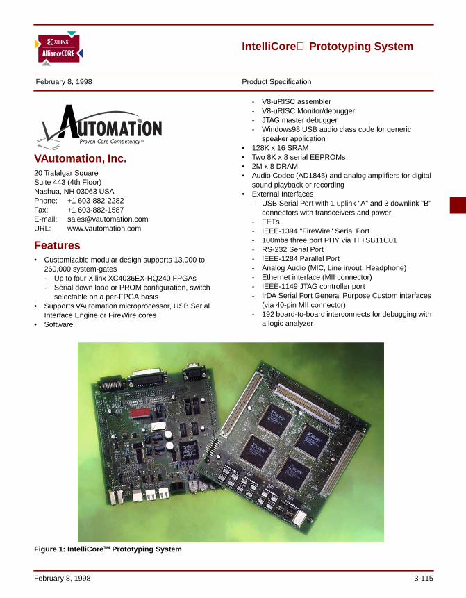
IntelliCore Prototyping System
February 8, 1998 Product Specification
VAutomation, Inc.20 Trafalgar SquareSuite 443 (4th Floor)Nashua, NH 03063 USA Phone: +1 603-882-2282Fax: +1 603-882-1587E-mail: [email protected]: www.vautomation.com
Features• Customizable modular design supports 13,000 to
260,000 system-gates- Up to four Xilinx XC4036EX-HQ240 FPGAs- Serial down load or PROM configuration, switch
selectable on a per-FPGA basis• Supports VAutomation microprocessor, USB Serial
Interface Engine or FireWire cores• Software
- V8-uRISC assembler- V8-uRISC Monitor/debugger- JTAG master debugger- Windows98 USB audio class code for generic
speaker application• 128K x 16 SRAM• Two 8K x 8 serial EEPROMs• 2M x 8 DRAM• Audio Codec (AD1845) and analog amplifiers for digital
sound playback or recording• External Interfaces
- USB Serial Port with 1 uplink "A" and 3 downlink "B" connectors with transceivers and power
- FETs- IEEE-1394 "FireWire" Serial Port- 100mbs three port PHY via TI TSB11C01- RS-232 Serial Port- IEEE-1284 Parallel Port- Analog Audio (MIC, Line in/out, Headphone)- Ethernet interface (MII connector)- IEEE-1149 JTAG controller port- IrDA Serial Port General Purpose Custom interfaces
(via 40-pin MII connector)- 192 board-to-board interconnects for debugging with
a logic analyzer
Figure 1: IntelliCore TM Prototyping System
February 8, 1998 3-115
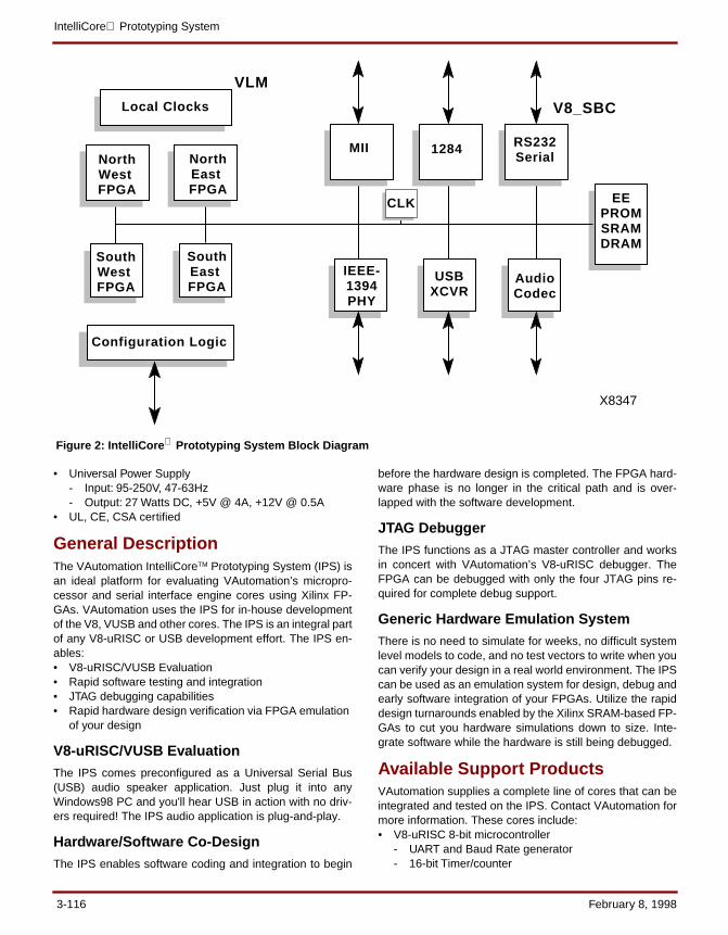
IntelliCore Prototyping System
• Universal Power Supply- Input: 95-250V, 47-63Hz- Output: 27 Watts DC, +5V @ 4A, +12V @ 0.5A
• UL, CE, CSA certified
General DescriptionThe VAutomation IntelliCoreTM Prototyping System (IPS) isan ideal platform for evaluating VAutomation’s micropro-cessor and serial interface engine cores using Xilinx FP-GAs. VAutomation uses the IPS for in-house developmentof the V8, VUSB and other cores. The IPS is an integral partof any V8-uRISC or USB development effort. The IPS en-ables:• V8-uRISC/VUSB Evaluation• Rapid software testing and integration• JTAG debugging capabilities• Rapid hardware design verification via FPGA emulation
of your design
V8-uRISC/VUSB EvaluationThe IPS comes preconfigured as a Universal Serial Bus(USB) audio speaker application. Just plug it into anyWindows98 PC and you'll hear USB in action with no driv-ers required! The IPS audio application is plug-and-play.
Hardware/Software Co-DesignThe IPS enables software coding and integration to begin
before the hardware design is completed. The FPGA hard-ware phase is no longer in the critical path and is over-lapped with the software development.
JTAG DebuggerThe IPS functions as a JTAG master controller and worksin concert with VAutomation’s V8-uRISC debugger. TheFPGA can be debugged with only the four JTAG pins re-quired for complete debug support.
Generic Hardware Emulation SystemThere is no need to simulate for weeks, no difficult systemlevel models to code, and no test vectors to write when youcan verify your design in a real world environment. The IPScan be used as an emulation system for design, debug andearly software integration of your FPGAs. Utilize the rapiddesign turnarounds enabled by the Xilinx SRAM-based FP-GAs to cut you hardware simulations down to size. Inte-grate software while the hardware is still being debugged.
Available Support ProductsVAutomation supplies a complete line of cores that can beintegrated and tested on the IPS. Contact VAutomation formore information. These cores include:• V8-uRISC 8-bit microcontroller
- UART and Baud Rate generator- 16-bit Timer/counter
Figure 2: IntelliCore Prototyping System Block Diagram
CLK
NorthWest FPGA
GFAdd
RS232Serial
EEPROMSRAMDRAM
Local Clocks
1284MII
USBXCVR
NorthEast FPGA
SouthWest FPGA
SouthEast FPGA
Configuration Logic
AudioCodec
IEEE-1394PHY
VLM
V8_SBC
X8347
3-116 February 8, 1998
VAutomation, Inc.
- IEEE 1284 parallel port- JTAG master/slave controller- DMA controller- DRAM controller
• VUSB USB target Serial Interface Engine
Ordering InformationThe VAutomation IntelliCore Prototyping System lists for$995.00 USD (limit two per customer) and comes completewith the following deliverables:• IPS electronics package
- VLM Logic Module PCB with one Xilinx XC4036HQ240-3 FPGA- V8/VUSB requires all of the resources of the
FPGA- Two and Four FPGA configurations also available
for application specific logic- V8_SBC PCB- Pretested and Verified
• V8 assembler.EXE file for DOS/Windows• V8 and VUSB Xilinx Configuration PROMs• V8 Monitor/Debugger burned into the EEPROM and on
a DOS format floppy• Windows98 compatible USB Audio Class code for
generic speakers• Universal Power Supply• IPS Users Manual• V8-uRISC Users Manual• VUSB Users Manual
To purchase or make further inquiries about this or otherVAutomation products, contact VAutomation directly.
Related Information
Xilinx Programmable LogicFor information on Xilinx programmable logic or develop-ment system software, contact your local Xilinx sales office,or:
Xilinx, Inc.2100 Logic DriveSan Jose, CA 95124Phone: +1 408-559-7778Fax: +1 408-559-7114URL: www.xilinx.com
For general Xilinx literature, contact:Phone: +1 800-231-3386 (inside the US)
+1 408-879-5017 (outside the US)E-mail: [email protected]
For AllianceCORE™ specific information, contact:Phone: +1 408-879-5381E-mail: [email protected]: www.xilinx.com/products/logicore/alliance/
tblpart.htm
February 8, 1998 3-117

3-118 February 8, 1998
IntelliCore Prototyping System
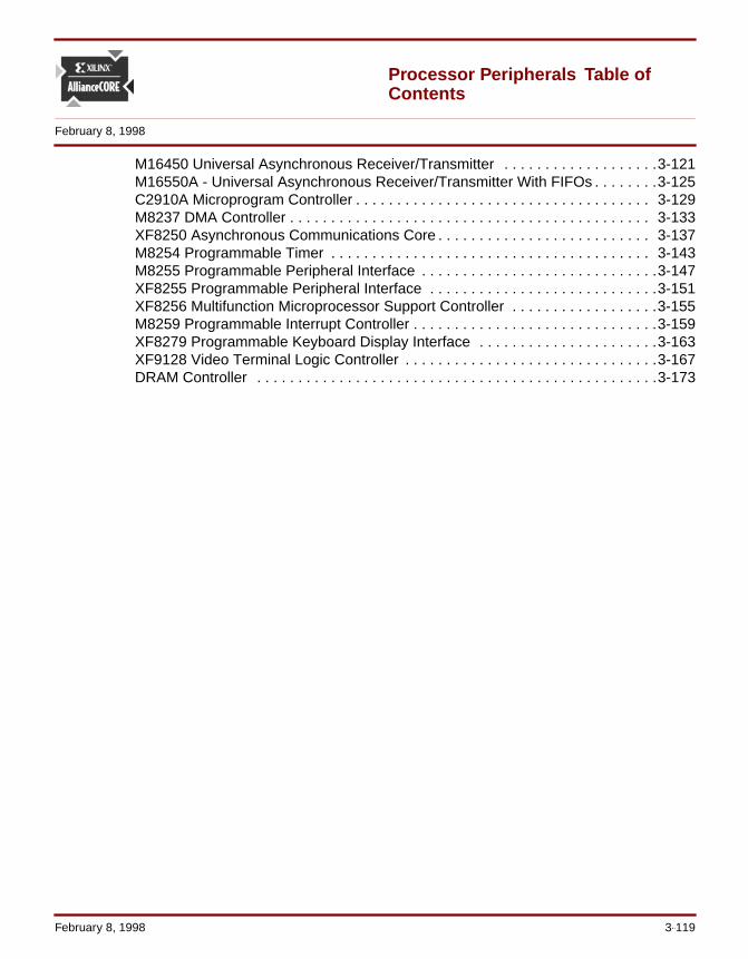
Processor Peripherals Table of Contents
February 8, 1998
M16450 Universal Asynchronous Receiver/Transmitter . . . . . . . . . . . . . . . . . . .3-121M16550A - Universal Asynchronous Receiver/Transmitter With FIFOs . . . . . . . .3-125C2910A Microprogram Controller . . . . . . . . . . . . . . . . . . . . . . . . . . . . . . . . . . . . 3-129M8237 DMA Controller . . . . . . . . . . . . . . . . . . . . . . . . . . . . . . . . . . . . . . . . . . . . 3-133XF8250 Asynchronous Communications Core . . . . . . . . . . . . . . . . . . . . . . . . . . 3-137M8254 Programmable Timer . . . . . . . . . . . . . . . . . . . . . . . . . . . . . . . . . . . . . . . 3-143M8255 Programmable Peripheral Interface . . . . . . . . . . . . . . . . . . . . . . . . . . . . .3-147XF8255 Programmable Peripheral Interface . . . . . . . . . . . . . . . . . . . . . . . . . . . .3-151XF8256 Multifunction Microprocessor Support Controller . . . . . . . . . . . . . . . . . .3-155M8259 Programmable Interrupt Controller . . . . . . . . . . . . . . . . . . . . . . . . . . . . . .3-159XF8279 Programmable Keyboard Display Interface . . . . . . . . . . . . . . . . . . . . . .3-163XF9128 Video Terminal Logic Controller . . . . . . . . . . . . . . . . . . . . . . . . . . . . . . .3-167DRAM Controller . . . . . . . . . . . . . . . . . . . . . . . . . . . . . . . . . . . . . . . . . . . . . . . . .3-173
February 8, 1998 3-119

Processor Peripherals Table of Contents
3-120 February 8, 1998
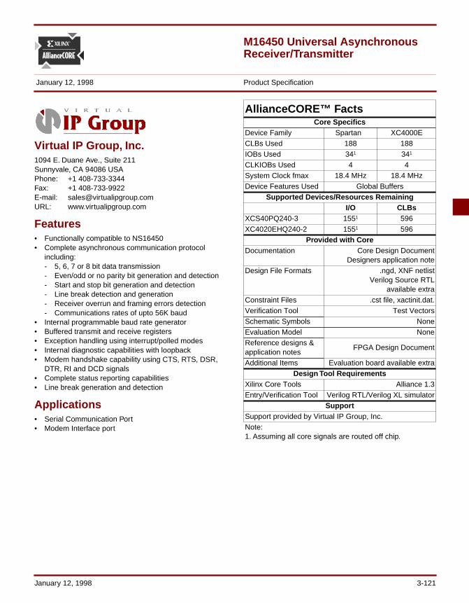
January 12, 1998 3-121
Virtual IP Group, Inc.1094 E. Duane Ave., Suite 211Sunnyvale, CA 94086 USAPhone: +1 408-733-3344Fax: +1 408-733-9922E-mail: [email protected]: www.virtualipgroup.com
Features• Functionally compatible to NS16450• Complete asynchronous communication protocol
including: - 5, 6, 7 or 8 bit data transmission- Even/odd or no parity bit generation and detection- Start and stop bit generation and detection- Line break detection and generation- Receiver overrun and framing errors detection- Communications rates of upto 56K baud
• Internal programmable baud rate generator• Buffered transmit and receive registers• Exception handling using interrupt/polled modes• Internal diagnostic capabilities with loopback• Modem handshake capability using CTS, RTS, DSR,
DTR, RI and DCD signals• Complete status reporting capabilities• Line break generation and detection
Applications• Serial Communication Port• Modem Interface port
AllianceCORE™ FactsCore Specifics
Device Family Spartan XC4000ECLBs Used 188 188IOBs Used 341 341
CLKIOBs Used 4 4System Clock fmax 18.4 MHz 18.4 MHzDevice Features Used Global Buffers
Supported Devices/Resources RemainingI/O CLBs
XCS40PQ240-3 1551 596XC4020EHQ240-2 1551 596
Provided with CoreDocumentation Core Design Document
Designers application noteDesign File Formats .ngd, XNF netlist
Verilog Source RTLavailable extra
Constraint Files .cst file, xactinit.dat.Verification Tool Test VectorsSchematic Symbols NoneEvaluation Model NoneReference designs & application notes
FPGA Design Document
Additional Items Evaluation board available extraDesign Tool Requirements
Xilinx Core Tools Alliance 1.3Entry/Verification Tool Verilog RTL/Verilog XL simulator
SupportSupport provided by Virtual IP Group, Inc.Note:1. Assuming all core signals are routed off chip.
M16450 Universal Asynchronous Receiver/Transmitter
January 12, 1998 Product Specification
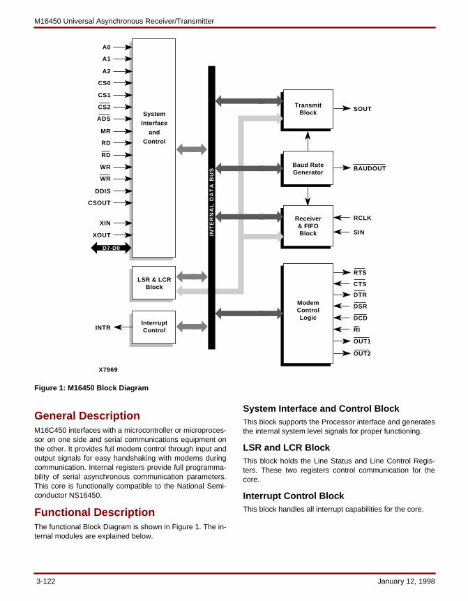
M16450 Universal Asynchronous Receiver/Transmitter
X7969
A0
A1
A2
CS0
SOUT
CS1
CS2
ADS
MR
RD
RD
WR
INTR
WR
DDIS
CSOUT
XIN
XOUT
System
Interface
and
Control
LSR & LCRBlock
TransmitBlock
InterruptControl
BAUDOUTBaud RateGenerator
RCLK
SIN
Receiver& FIFOBlock
RTS
OUT1
OUT2
CTS
DSR
DCD
RI
DTRModemControlLogic
D7-D0
INT
ER
NA
L D
AT
A B
US
General DescriptionM16C450 interfaces with a microcontroller or microproces-sor on one side and serial communications equipment onthe other. It provides full modem control through input andoutput signals for easy handshaking with modems duringcommunication. Internal registers provide full programma-bility of serial asynchronous communication parameters.This core is functionally compatible to the National Semi-conductor NS16450.
Functional DescriptionThe functional Block Diagram is shown in Figure 1. The in-ternal modules are explained below.
System Interface and Control BlockThis block supports the Processor interface and generatesthe internal system level signals for proper functioning.
LSR and LCR BlockThis block holds the Line Status and Line Control Regis-ters. These two registers control communication for thecore.
Interrupt Control BlockThis block handles all interrupt capabilities for the core.
Figure 1: M16450 Block Diagram
3-122 January 12, 1998
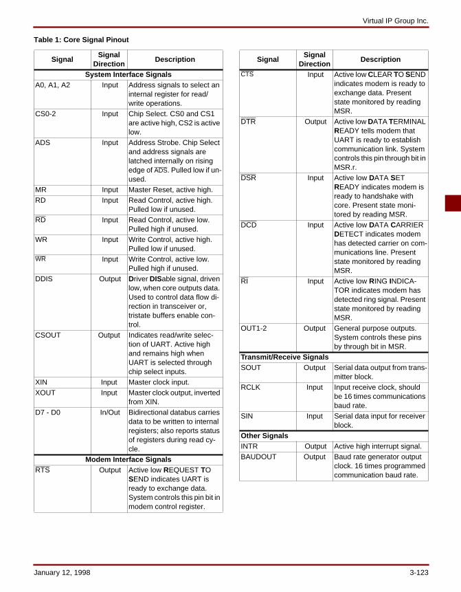
Virtual IP Group Inc.
Table 1: Core Signal Pinout
SignalSignal
DirectionDescription
System Interface SignalsA0, A1, A2 Input Address signals to select an
internal register for read/write operations.
CS0-2 Input Chip Select. CS0 and CS1 are active high, CS2 is active low.
ADS Input Address Strobe. Chip Select and address signals are latched internally on rising edge of ADS. Pulled low if un-used.
MR Input Master Reset, active high.RD Input Read Control, active high.
Pulled low if unused.RD Input Read Control, active low.
Pulled high if unused.WR Input Write Control, active high.
Pulled low if unused.WR Input Write Control, active low.
Pulled high if unused.DDIS Output Driver DISable signal, driven
low, when core outputs data. Used to control data flow di-rection in transceiver or, tristate buffers enable con-trol.
CSOUT Output Indicates read/write selec-tion of UART. Active high and remains high when UART is selected through chip select inputs.
XIN Input Master clock input. XOUT Input Master clock output, inverted
from XIN.D7 - D0 In/Out Bidirectional databus carries
data to be written to internal registers; also reports status of registers during read cy-cle.
Modem Interface SignalsRTS Output Active low REQUEST TO
SEND indicates UART is ready to exchange data. System controls this pin bit in modem control register.
SignalSignal
DirectionDescription
CTS Input Active low CLEAR TO SEND indicates modem is ready to exchange data. Present state monitored by reading MSR.
DTR Output Active low DATA TERMINAL READY tells modem that UART is ready to establish communication link. System controls this pin through bit in MSR.r.
DSR Input Active low DATA SET READY indicates modem is ready to handshake with core. Present state moni-tored by reading MSR.
DCD Input Active low DATA CARRIER DETECT indicates modem has detected carrier on com-munications line. Present state monitored by reading MSR.
RI Input Active low RING INDICA-TOR indicates modem has detected ring signal. Present state monitored by reading MSR.
OUT1-2 Output General purpose outputs. System controls these pins by through bit in MSR.
Transmit/Receive Signals SOUT Output Serial data output from trans-
mitter block. RCLK Input Input receive clock, should
be 16 times communications baud rate.
SIN Input Serial data input for receiver block.
Other Signals INTR Output Active high interrupt signal. BAUDOUT Output Baud rate generator output
clock. 16 times programmed communication baud rate.
January 12, 1998 3-123
M16450 Universal Asynchronous Receiver/Transmitter
Transmit BlockThis block controls serial data transmission as per pro-grammed parameters.
Baud Rate Generator BlockThis block generates the Baud Rate Clock for the transmit-ter section of the core. This clock can also be used by thereceiver block connecting BAUDOUT to RCLK.
Receiver BlockThis block handles reception for the core. The clock for thisblock is provided by RCLK. This clock should be 16 timesthe baud rate.
Modem Control Logic BlockThis block handles modem handshaking for the core.These signals can be used for communication or as generalpurpose signals. The modem control register resides in thisblock, providing internal diagnostic capability.
Core ModificationsModifications can be done to remove the internal baud rategenerator, or to strip off either transmitter or receiver.These modifications can be performed by Virtual IP Group,Inc. for additional cost.
PinoutThe pinout has not been fixed to a specific FPGA/IO allow-ing flexibility with the user application. A pinout is suggest-ed for use with a user-constructible evaluation board.Information for this is in the FPGA Design Document includ-ed with the core. Signal names are provided in the block di-agram shown in Figure 1 and Table 1.
Verification MethodsThe core has been tested with in-house developed simula-tion test vectors that are provided with the core. Assemblylevel 80x86 programs were used to test the functionality ofthe FPGA using a hardware evaluation board.
Recommended Design ExperienceKnowledge of interface with Microprocessor based sys-tems is required. The user must be familiar with HDL design
methodology as well as instantiation of Xilinx netlists in ahierarchical design environment. Usage of Alliance orFoundation tools is required.
Available Support ProductsThe FPGA Design Document included with the core givesdirections of constructing a general purpose FPGA evalua-tion daughter board that can be plugged in to a standardport socket on the target system through a flat cable.
Ordering InformationThis product is available from Virtual IP Group, Inc. Pleasecontact them for pricing and additional information.
Related InformationRefer to Specification Document for programming of thiscore for a typical application in a system. The user isrequired to refer to Designer’s application note for integrat-ing this core with other cores.
Xilinx Programmable LogicFor information on Xilinx programmable logic or develop-ment system software, contact your local Xilinx sales office,or:
Xilinx, Inc.2100 Logic DriveSan Jose, CA 95124Phone: +1 408-559-7778Fax: +1 408-559-7114URL: www.xilinx.com
For general Xilinx literature, contact:
Phone: +1 800-231-3386 (inside the US)+1 408-879-5017 (outside the US)
E-mail: [email protected]
For AllianceCORETM specific information, contact:
Phone: +1 408-879-5381E-mail: [email protected]: www.xilinx.com/products/logicore/alliance/
tblpart.htm
3-124 January 12, 1998
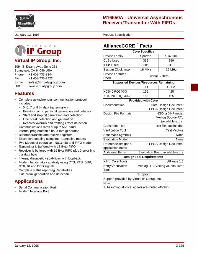
M16550A - Universal Asynchronous Receiver/Transmitter With FIFOs
January 12, 1998 Product Specification
Virtual IP Group, Inc.1094 E. Duane Ave., Suite 211 Sunnyvale, CA 94086 USAPhone: +1 408-733-3344Fax: +1 408-733-9922E-mail: [email protected] : www.virtualipgroup.com
Features• Complete asynchronous communication protocol
includes: - 5, 6, 7 or 8 bit data transmission- Even/odd or no parity bit generation and detection.- Start and stop bit generation and detection.- Line break detection and generation.- Receiver overrun and framing errors detection
• Communications rates of up to 56K baud• Internal programmable baud rate generator• Buffered transmit and receive registers• Exception handling using interrupt/polled modes• Two Modes of operation - NS16450 and FIFO mode• Transmitter is buffered with 16 Byte FIFO• Receiver is buffered with 16 Byte FIFO plus 3 error bits
per data byte• Internal diagnostic capabilities with loopback• Modem handshake capability using CTS, RTS, DSR,
DTR, RI and DCD signals• Complete status reporting Capabilities• Line break generation and detection
Applications• Serial Communication Port• Modem Interface Port
AllianceCORE ™ FactsCore Specifics
Device Family Spartan XC4000ECLBs Used 359 359IOBs Used 381 381
System Clock fmax 16 MHz 16 MHzDevice Features Used
Global Buffers
Supported Devices/Resources RemainingI/O CLBs
XCS40 PQ240-3 155 425XC4020E HQ240-2 155 425
Provided with CoreDocumentation Core Design Document
FPGA Design DocumentDesign File Formats NGD or XNF netlist
Verilog Source RTL (available extra)
Constraint Files .cst file, xactinit.dat.Verification Tool Test VectorsSchematic Symbols NoneEvaluation Model NoneReference designs & application notes
FPGA Design Document
Additional Items Evaluation Board available extraDesign Tool Requirements
Xilinx Core Tools Alliance 1.3Entry/Verification Tool
Verilog RTL/Verilog XL simulator
SupportSupport provided by Virtual IP Group, Inc.Note:1. Assuming all core signals are routed off-chip.
January 12, 1998 3-125
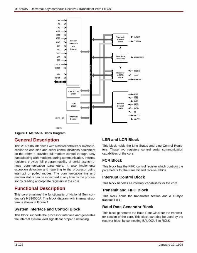
M16550A - Universal Asynchronous Receiver/Transmitter With FIFOs
General DescriptionThe M16550A interfaces with a microcontroller or micropro-cessor on one side and serial communications equipmenton the other. It provides full modem control through easyhandshaking with modems during communication. Internalregisters provide full programmability of serial asynchro-nous communication parameters. It also implementsexception detection and reporting to the processor usinginterrupt or polled modes. The communication line andmodem status can be monitored at any time by the proces-sor by reading appropriate registers in the core.
Functional DescriptionThis core emulates the functionality of National Semicon-ductor’s NS16550A. The block diagram with internal struc-ture is shown in Figure 1.
System Interface and Control BlockThis block supports the processor interface and generatesthe internal system level signals for proper functioning.
LSR and LCR BlockThis block holds the Line Status and Line Control Regis-ters. These two registers control serial communicationcapabilities of the core.
FCR BlockThis block has the FIFO control register which controls theparameters for the transmit and receive FIFOs.
Interrupt Control BlockThis block handles all interrupt capabilities for the core.
Transmit and FIFO BlockThis block holds the transmitter section and a 16-bytetransmit FIFO.
Baud Rate Generator BlockThis block generates the Baud Rate Clock for the transmit-ter section of the core. This clock can also be used by thereceiver block by connecting BAUDOUT to RCLK
D7
-
X7975
A0
A1
A2
CS0
SOUT
TXRDY
CS1
CS2
ADS
MR
RD
RD
WR
INTR
WR
NCS
DDIS
XIN
XOUT
System
Interface
and
Control
LSR & LCRBlock
Transmit& FIFOBlock
FCRBlock
InterruptControl
BAUDOUTBaud RateGenerator
RCLK
SIN
RXRDY
Receiver& FIFOBlock
RTS
OUT1
OUT2
CTS
DSR
DCD
RI
DTRModemControlLogic
D7-D0
INT
ER
NA
L D
AT
A B
US
Figure 1: M16550A Block Diagram
3-126 January 12, 1998
January 12, 1998 3-127
Virtual IP Group Inc.
Table 1: Core Signal Pinout
SignalSignal
DirectionDescription
System Interface SignalsA0, A1, A2 Input Address signals to select an
internal register for read/write operations.
CS0-2 Input Chip Select. CS0 and CS1 are active high, CS2 is active low.
ADS Input Address Strobe. Chip Select, and address signals are latched internally on rising edge of ADS. Pulled low if un-used.
MR Input Master Reset Signal, active high.
RD Input Control, active high. Pulled low if unused.
RD Input Control, active low. Pulled high if unused.
WR Input Control, active high. Pulled low if unused.
WR Input Write Control, active low. Pulled high if unused.
DDIS Output Driver DISable signal, driven low, when core outputs data. Used to control data flow di-rection intransceiver, or tristate buffers enable con-trol.
CSOUT Output Indicates read/write selec-tion of UART, active high and remains high when UART is selected through chip select inputs.
XIN Input Master clock input. XOUT Input Master clock output, inverted
from XIN.D7 - D0 In/Out Bidirectional databus carries
data to be written to internal registers; also reports status of registers during read cy-cle.
Modem Interface SignalsRTS Output Active low REQUEST TO
SEND indicates UART is ready to exchange data. Sys-tem controls this pin through bit in modem control register.
CTS Input Active low CLEAR TO SEND indicates modem is ready to exchange data. Present state monitored by reading MSR.
DTR Output Active low DATA TERMINAL READY tells modem that UART is ready to establish communication link. System controls this pin by program-ming a bit in MSR.
DSR Input Active low DATA SET READY indicates modem is ready to handshake with core. Present state moni-tored by reading MSR.
DCD Input Active low DATA CARRIER DETECT indicates modem has detected carrier on com-munications line. Present state monitored by reading MSR.
RI Input Active low RING INDICA-TOR indicates modem has detected ring signal. Present state monitored by reading MSR.
OUT1-2 Output General purpose outputs. System controls these pins by through bit in MSR.
Transmit/Receive Signals SOUT Output Serial data output from trans-
mitter block. RCLK Input Input receive clock, should
be 16 times communications baud rate.
SIN Input Serial data input for receiver block.
Other Signals INTR Output Active high interrupt signal. BAUDOUT Output Baud rate generator output
clock.16 times the pro-grammed communication baud rate.
SignalSignal
DirectionDescription
M16550A - Universal Asynchronous Receiver/Transmitter With FIFOs
Receiver and FIFO BlockThis block handles reception for the core. The clock for thisblock is provided by RCLK. This clock should be 16X theBaud Rate. The receive data FIFO is included in this blockwhich stores 16 bytes at a time. The 16 bit FIFO’s for statusparameters (parity, framing and break) for the correspond-ing bytes in the receiver data FIFO is also included in thisblock.
Modem Control Logic BlockThis block handles the modem control capabilities for themegacell core. These signals can be used for the commu-nication purpose also some of the signals can be used asgeneral purpose signals (OUT1 and OUT2). The modemcontrol register resides in this block which provides theinternal diagnostic capability for the core.
Core ModificationsModifications can be done to remove the internal baud rategenerator, or strip off either transmitter or receiver or sizethe FIFO of Transmitter and Receiver separately. Thesemodifications can be performed by Virtual IP Group, Inc. foradditional cost.
PinoutThe pinout has not been fixed to specific FPGA I/O allowingflexibility with the users application. The evaluation boardpinout, however has been fixed. This information isincluded in the design documentation. Signal names areprovided in the block diagram shown in Figure 1 and Table1.
Verification MethodsThe core has been tested with in-house developed simula-tion test vectors that are provided with the core. Assemblylevel 80x86 programs were used to test the functionality ofthe FPGA in hardware.
Recommended Design ExperienceKnowledge of interface with Microprocessor based sys-tems is required. The user must be familiar with HDL designmethodology as well as instantiation of Xilinx netlists in a
hierarchical design environment. Usage of Alliance orFoundation tools is required.
Available Support ProductsThe FPGA Design Document included with the core givesdirections of constructing a general purpose FPGA evalua-tion daughter board that can be plugged in to a standardport socket on the target system through a flat cable.
Ordering InformationThis product is available from Virtual IP Group, Inc. Pleasecontact them for pricing and additional information.
Related InformationRefer to Specification Document for programming of thiscore for a typical application in a system. The user isrequired to refer to Designer’s application note for integrat-ing this core with other cores.
Xilinx Programmable LogicFor information on Xilinx programmable logic or develop-ment system software, contact your local Xilinx sales office,or:
Xilinx, Inc.2100 Logic DriveSan Jose, CA 95124Phone: +1 408-559-7778Fax: +1 408-559-7114URL: www.xilinx.com
For general Xilinx literature, contact:
Phone: +1 800-231-3386 (inside the US)+1 408-879-5017 (outside the US)
E-mail: [email protected]
For AllianceCORETM specific information, contact:
Phone: +1 408-879-5381E-mail: [email protected]: www.xilinx.com/products/logicore/alliance/
tblpart.htm
3-128 January 12, 1998
C2910A Microprogram Controller
January 12, 1998 Product Specification
CAST, Inc.24 White Birch DrivePomona, New York 10907 USAPhone: +1 914-354-4945Fax: +1 914-354-0325E-Mail: [email protected] : www.cast-inc.com
Features• Based on the AMD2910A device• Pre-defined implementation for predictable timing • Verified against a hardware model of the original device• 12-bit data width that addresses up to 4,096 words• Internal loop counter - pre-settable 12-bit down-counter
for repeating instructions and counting loop interactions• Four address sources
- Microprogram counter- Branch address bus- 9-level push/pop stack- Internal holding register
• 16 powerful microinstructions• Output Enable Controls for three branch address
sources• Positive-edge-triggered registers
Applications The C2910A core is used in high speed bit slice designs.
General DescriptionThe C2910A microprogram controller core is an addresssequencer that controls the sequence of execution for themicroinstructions stored in microprogram memory. Thecore can sequentially access the microinstructions, and itprovides conditional branching to any microinstructionswithin the 4,096-microword range. In addition, a nine-deepLIFO stack provides a microsubroutine return linkage andlooping capability.
Notes:1. Assuming all core signals are routed off-chip.
AllianceCORE™ FactsCore Specifics
Device Family Spartan XC4005XLCLBs Used 185 185IOBs Used 381 381
System Clock fmax 27.7 MHz 34.5 MHzDevice Features Used
Global Buffers
Supported Devices/Resources RemainingI/O CLBs
XC4005XL-09 751 11
XCS10-3 751 11
Provided with CoreDocumentation Core DocumentationDesign File Formats XNF Netlist
VHDL Source RTLConstraint Files NCFVerification Tool Test Bench
Test VectorsSchematic Symbols ViewlogicEvaluation Model VHDL behavioral modelReference designs & application notes
None
Additional Items NoneDesign Tool Requirements
Xilinx Core Tools M1.3Entry/Verification Tool
1076 compliant VHDL Simulator
SupportSupport provided by CAST, Inc.
January 12, 1998 3-129
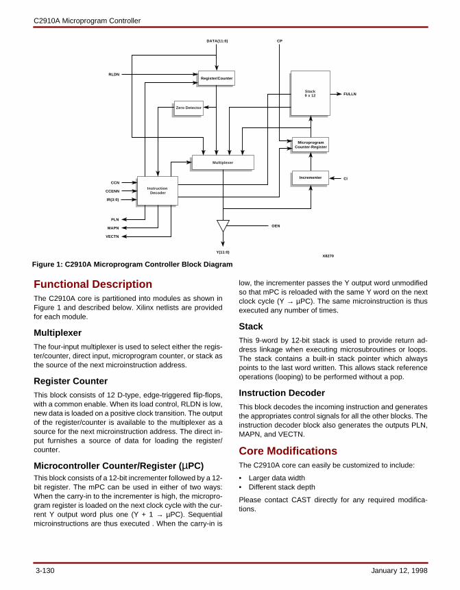
C2910A Microprogram Controller
Functional DescriptionThe C2910A core is partitioned into modules as shown inFigure 1 and described below. Xilinx netlists are providedfor each module.
MultiplexerThe four-input multiplexer is used to select either the regis-ter/counter, direct input, microprogram counter, or stack asthe source of the next microinstruction address.
Register CounterThis block consists of 12 D-type, edge-triggered flip-flops,with a common enable. When its load control, RLDN is low,new data is loaded on a positive clock transition. The outputof the register/counter is available to the multiplexer as asource for the next microinstruction address. The direct in-put furnishes a source of data for loading the register/counter.
Microcontroller Counter/Register ( µPC)This block consists of a 12-bit incrementer followed by a 12-bit register. The mPC can be used in either of two ways:When the carry-in to the incrementer is high, the micropro-gram register is loaded on the next clock cycle with the cur-rent Y output word plus one (Y + 1 → µPC). Sequentialmicroinstructions are thus executed . When the carry-in is
low, the incrementer passes the Y output word unmodifiedso that mPC is reloaded with the same Y word on the nextclock cycle (Y → µPC). The same microinstruction is thusexecuted any number of times.
Stack This 9-word by 12-bit stack is used to provide return ad-dress linkage when executing microsubroutines or loops.The stack contains a built-in stack pointer which alwayspoints to the last word written. This allows stack referenceoperations (looping) to be performed without a pop.
Instruction Decoder This block decodes the incoming instruction and generatesthe appropriates control signals for all the other blocks. Theinstruction decoder block also generates the outputs PLN,MAPN, and VECTN.
Core ModificationsThe C2910A core can easily be customized to include:
• Larger data width• Different stack depth
Please contact CAST directly for any required modifica-tions.
X8270
DATA(11:0)
FULLN
Y(11:0)
MicroprogramCounter-Register
Register/Counter
IR(3:0)
CCN
CCENN
VECTN
PLN
MAPN
RLDN
CI
OEN
CP
Zero Detector
Stack9 x 12
Multiplexer
Instruction Decoder
Incrementer
Figure 1: C2910A Microprogram Controller Block Diagram
3-130 January 12, 1998
Cast Inc.
PinoutThe pinout of the C2910A core has not been fixed to spe-cific FPGA I/O, allowing flexibility with a users application.Signal names are shown in the block diagram in Figure 1,and in Table 1.
Table 1: Core Signal Pinout
Core Assumptions
Stack PUSHAfter a depth of 9 is reached, the stack is full and the FULLNoutput goes LOW. If further PUSHes are attempted whenthe stack is full, the stack information at the top of the stack(9) will be over-written.
It has been observed that the AM2910A device inconsis-tently destroys the top 2 locations of the stack (8 and 9).This functionality is apparently not documented, and shouldnot be relied upon.
Stack POPFurther POPs from an empty stack will place the bottomdata on the Y-Bus (no changes). Is has been observed thatthe AM2910A device will place random data in the Y-Busduring POPs from an empty stack.
To achieve proper result, do not exercise the stack beyondits range (i.e. no PUSHes while the stack is full and noPOPs while stack is empty).
Verification MethodsThe C2910A Microprogram Controller core’s functionalitywas verified by means of a proprietary hardware modeler.
The same stimulus was applied to a hardware model whichcontained the original AM2910A chip, and the results com-pared with the core’s simulation outputs.The C2910A corehas also been successfully implemented into silicon.
Recommended Design ExperienceThe user must be familiar with HDL design methodology aswell as instantiation of Xilinx netlists in a hierarchical designenvironment.
Ordering InformationThis product is available from CAST, Inc. Please contactCAST for pricing and more information.
Related Information
Bipolar Microprocessor Logic and Interface Data BookContact:
Advanced Micro DevicesOne AMD PlaceP.O. Box 3453Sunnyvale, California 94088-3453Phone: 408-732-2400
800-538-8450800-222-9323 (literature)
E-mail: [email protected]: www.amd.com
Xilinx Programmable LogicFor information on Xilinx programmable logic or develop-ment system software, contact your local Xilinx sales office,or:
Xilinx, Inc.2100 Logic DriveSan Jose, CA 95124Phone: +1 408-559-7778Fax: +1 408-559-7114URL: www.xilinx.com
For general Xilinx literature, contact:
Phone: +1 800-231-3386 (inside the US)+1 408-879-5017 (outside the US)
E-mail: [email protected]
For AllianceCORE™ specific information, contact:
Phone: +1 408-879-5381E-mail: [email protected]: www.xilinx.com/products/logicore/alliance/
tblpart.htm
SignalSignal
DirectionDescription
CP Input ClockIR (3:0) Input InstructionDATA (11:0) Input Direct DataCCN Input Condition CodeCCENN Input Condition Code Enable RLDN Input Register Load EnableCI Input Carry-InOEN Input Output EnableY (11:0) Output Microprogram AddressFULLN Output Full FlagPLN Output Pipeline Address EnableMAPN Output Map Address Enable VECTN Output Vector Address Enable
January 12, 1998 3-131

C2910A Microprogram Controller
3-132 January 12, 1998
M8237 DMA Controller
February 8, 1998 Product Specification
Virtual IP Group, Inc.1094 E. Duane Ave., Suite 211 Sunnyvale, CA 94086 USAPhone: +1 408-733-3344Fax: +1 408-733-9922E-mail: [email protected]: www.virtualipgroup.com
Features• Multimode Direct Memory Access (DMA) controller• Functionally compatible to Intel 8237• Four independent DMA channels• Independent auto-initialization of all channels• Directly expandable to any number of channels• Memory-to-memory transfers• Memory block initialization• Enable/disable control of individual DMA requests• Address increment/decrement selection control for all
channels• High performance transfers up to 1.6 MBytes/second
with 5 MHz• End of process input to terminate transfers• Software DMA request• Programmable polarity control for DMA Request and
DACK signals
Applications• Multi-mode Programmable, multi-channel DMA • Support Controller for Microprocessor based systems
AllianceCORE ™ FactsCore Specifics
Device Family XC4000ECLBs Used 392IOBs Used 371
CLKIOBS used 1System Clock fmax 8 MHzDevice Features Used
Global buffers
Supported Devices/Resources RemainingI/O CLBs
XC4036EX HQ240-4 1561 904Provided with Core
Documentation Core Design DocumentDesigner’s Application Note
Design File Formats .ngd, XNF netlist Verilog Source RTL
(available extra)Constraint Files .cst file, xactinit.datVerification Tool Test VectorsSchematic Symbols NoneEvaluation Model NoneReference designs & application notes
FPGA Design Documentincluded
Additional Items NoneDesign Tool Requirements
Xilinx Core Tools Alliance 1.3Entry/Verification Tool
Verilog RTL/Verilog XL Simulator
SupportSupport provided by Virtual IP Group, Inc.Note:1. Assuming all core signals are routed off-chip.
February 8, 1998 3-133
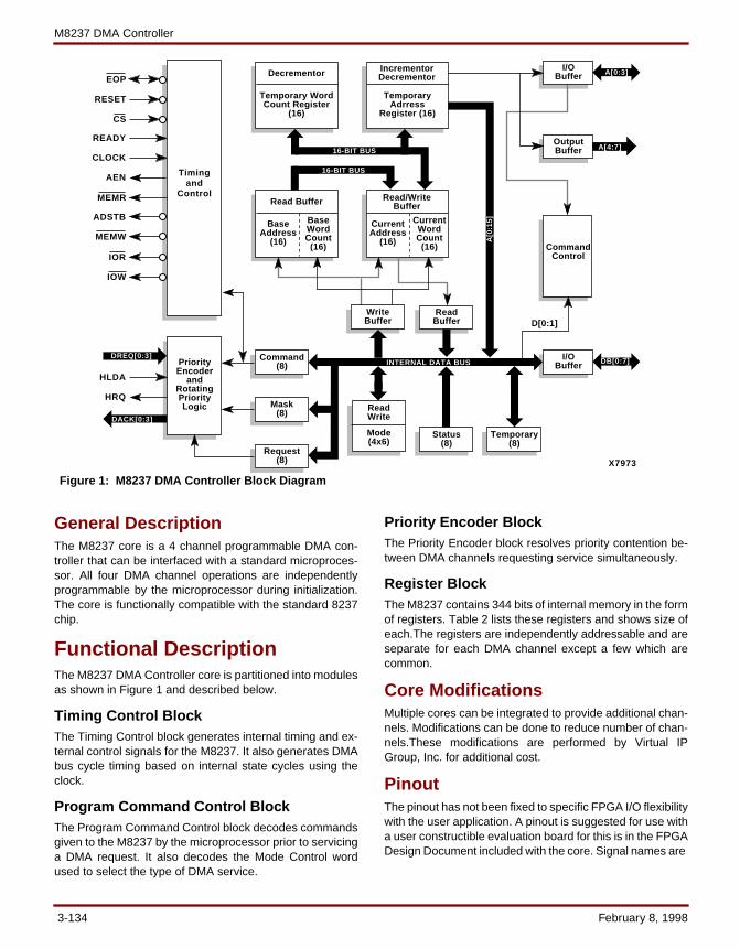
M8237 DMA Controller
General DescriptionThe M8237 core is a 4 channel programmable DMA con-troller that can be interfaced with a standard microproces-sor. All four DMA channel operations are independentlyprogrammable by the microprocessor during initialization.The core is functionally compatible with the standard 8237chip.
Functional DescriptionThe M8237 DMA Controller core is partitioned into modulesas shown in Figure 1 and described below.
Timing Control BlockThe Timing Control block generates internal timing and ex-ternal control signals for the M8237. It also generates DMAbus cycle timing based on internal state cycles using theclock.
Program Command Control BlockThe Program Command Control block decodes commandsgiven to the M8237 by the microprocessor prior to servicinga DMA request. It also decodes the Mode Control wordused to select the type of DMA service.
Priority Encoder BlockThe Priority Encoder block resolves priority contention be-tween DMA channels requesting service simultaneously.
Register BlockThe M8237 contains 344 bits of internal memory in the formof registers. Table 2 lists these registers and shows size ofeach.The registers are independently addressable and areseparate for each DMA channel except a few which arecommon.
Core ModificationsMultiple cores can be integrated to provide additional chan-nels. Modifications can be done to reduce number of chan-nels.These modifications are performed by Virtual IPGroup, Inc. for additional cost.
PinoutThe pinout has not been fixed to specific FPGA I/O flexibilitywith the user application. A pinout is suggested for use witha user constructible evaluation board for this is in the FPGADesign Document included with the core. Signal names are
WriteBuffer
Read Buffer
BaseAddress
(16)
BaseWordCount
(16)
X7973
EOP
READY
CLOCK
AEN Timingand
Control
ADSTB
RESET
CS
MEMR
MEMW
IOR
IOW
Status(8)
ReadBuffer
Command(8)Priority
Encoderand
RotatingPriorityLogic Mask
(8)
Request(8)
ReadWrite
Mode(4x6)
Temporary(8)
I/OBuffer
D[0:1]
CommandControl
Read/WriteBuffer
CurrentAddress
(16)
CurrentWordCount
(16)
Decrementor
Temporary WordCount Register
(16)
IncrementorDecrementor
INTERNAL DATA BUS DB[0:7]
OutputBuffer
A[0:3]
TemporaryAdrress
Register (16)
16-BIT BUS
16-BIT BUS
A[0
:15]
HLDA
HRQ
DREQ[0:3]
DACK[0:3]
I/OBuffer
A[4:7]
Figure 1: M8237 DMA Controller Block Diagram
3-134 February 8, 1998
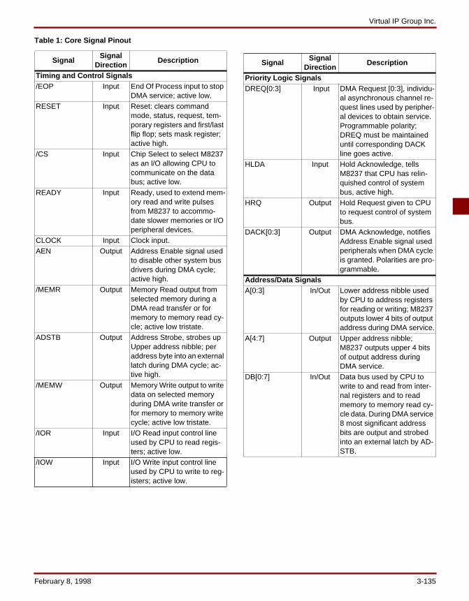
Virtual IP Group Inc.
Table 1: Core Signal Pinout
SignalSignal
DirectionDescription
Timing and Control Signals/EOP Input End Of Process input to stop
DMA service; active low.RESET Input Reset: clears command
mode, status, request, tem-porary registers and first/last flip flop; sets mask register; active high.
/CS Input Chip Select to select M8237 as an l/O allowing CPU to communicate on the data bus; active low.
READY Input Ready, used to extend mem-ory read and write pulses from M8237 to accommo-date slower memories or I/O peripheral devices.
CLOCK Input Clock input.AEN Output Address Enable signal used
to disable other system bus drivers during DMA cycle; active high.
/MEMR Output Memory Read output from selected memory during a DMA read transfer or for memory to memory read cy-cle; active low tristate.
ADSTB Output Address Strobe, strobes up Upper address nibble; per address byte into an external latch during DMA cycle; ac-tive high.
/MEMW Output Memory Write output to write data on selected memory during DMA write transfer or for memory to memory write cycle; active low tristate.
/IOR Input I/O Read input control line used by CPU to read regis-ters; active low.
/IOW Input I/O Write input control line used by CPU to write to reg-isters; active low.
SignalSignal
DirectionDescription
Priority Logic SignalsDREQ[0:3] Input DMA Request [0:3], individu-
al asynchronous channel re-quest lines used by peripher-al devices to obtain service. Programmable polarity; DREQ must be maintained until corresponding DACK line goes active.
HLDA Input Hold Acknowledge, tells M8237 that CPU has relin-quished control of system bus, active high.
HRQ Output Hold Request given to CPU to request control of system bus.
DACK[0:3] Output DMA Acknowledge, notifies Address Enable signal used peripherals when DMA cycle is granted. Polarities are pro-grammable.
Address/Data SignalsA[0:3] In/Out Lower address nibble used
by CPU to address registers for reading or writing; M8237 outputs lower 4 bits of output address during DMA service.
A[4:7] Output Upper address nibble; M8237 outputs upper 4 bits of output address during DMA service.
DB[0:7] In/Out Data bus used by CPU to write to and read from inter-nal registers and to read memory to memory read cy-cle data. During DMA service 8 most significant address bits are output and strobed into an external latch by AD-STB.
February 8, 1998 3-135
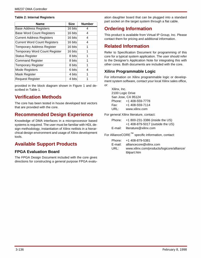
M8237 DMA Controller
Table 2: Internal Registers
provided in the block diagram shown in Figure 1 and de-scribed in Table 1.
Verification MethodsThe core has been tested in house developed test vectorsthat are provided with the core.
Recommended Design ExperienceKnowledge of DMA interfaces in a microprocessor basedsystems is required. The user must be familiar with HDL de-sign methodology, instantiation of Xilinx netlists in a hierar-chical design environment and usage of Xilinx developmenttools.
Available Support Products
FPGA Evaluation BoardThe FPGA Design Document included with the core givesdirections for constructing a general purpose FPGA evalu-
ation daughter board that can be plugged into a standardpart socket on the target system through a flat cable.
Ordering InformationThis product is available from Virtual IP Group, Inc. Pleasecontact them for pricing and additional information.
Related InformationRefer to Specification Document for programming of thiscore for a typical system application. The user should referto the Designer's Application Note for integrating this withother cores. Both documents are included with the core.
Xilinx Programmable LogicFor information on Xilinx programmable logic or develop-ment system software, contact your local Xilinx sales office,or:
Xilinx, Inc.2100 Logic DriveSan Jose, CA 95124Phone: +1 408-559-7778Fax: +1 408-559-7114URL: www.xilinx.com
For general Xilinx literature, contact:
Phone: +1 800-231-3386 (inside the US)+1 408-879-5017 (outside the US)
E-mail: [email protected]
For AllianceCORE™ specific information, contact:
Phone: +1 408-879-5381E-mail: [email protected]: www.xilinx.com/products/logicore/alliance/
tblpart.htm
Name Size NumberBase Address Registers 16 bits 4Base Word Count Registers 16 bits 4Current Address Registers 16 bits 4Current Word Count Registers 16 bits 4Temporary Address Register 16 bits 1Temporary Word Count Register 16 bits 1Status Register 8 bits 1Command Register 8 bits 1Temporary Register 8 bits 1Mode Registers 6 bits 4Mask Register 4 bits 1Request Register 4 bits 1
3-136 February 8, 1998
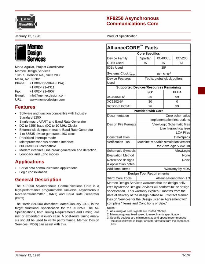
XF8250 Asynchronous Communications Core
January 12, 1998 Product Specification
Maria Aguilar, Project Coordinator Memec Design Services 1819 S. Dobson Rd., Suite 203 Mesa, AZ 85202 Phone: +1 888-360-9044 (USA)
+1 602-491-4311Fax: +1 602-491-4907 E-mail: [email protected]: www.memecdesign.com
Features• Software and function compatible with Industry
Standard 8250• Single macro UART and Baud Rate Generator• DC to 625K baud (DC to 10 MHz Clock) • External clock input In-macro Baud Rate Generator• 1 to 65535 divisor generates 16X clock • Prioritized interrupt mode • Microprocessor bus oriented interface • 80C86/80C88 compatible • Modem interface Line break generation and detection• Loopback and Echo modes
Applications• Serial data communications applications • Logic consolidation
General Description The XF8250 Asynchronous Communications Core is ahigh-performance programmable Universal AsynchronousReceiver/Transmitter (UART) and Baud Rate Generator(BRG).
The Harris 82C50A datasheet, dated January 1992, is thetarget functional specification for the XF8250. The ACSpecifications, both Timing Requirements and Timing, aremet or exceeded in every case. A post-route timing analy-sis should be used to verify performance. Memec DesignServices (MDS) can assist with this.
AllianceCORE ™ FactsCore Specifics
Device Family Spartan XC4000E XC5200CLBs Used 97 97 64IOBs Used 351
Systems Clock fmax 10+ MHz2
Device Features Used
Tbufs, global clock buffers
Supported Devices/Resources RemainingI/O1 CLBs
XC4005E-63 26 99XC5202-63 30 0XCS05-3 PC843 26 99
Provided with CoreDocumentation Core schematics
Implementation instructionsDesign File Formats ViewLogic Schematic files
Live hierarchical treeLCA Files
Constraint Files TimeSpecsVerification Tool Machine-readable simulation vectors
for ViewLogic ViewSimSchematic Symbols ViewLogicEvaluation Method NoneReference designs & application notes
None
Additional Items Warranty by MDSDesign Tool Requirements
Xilinx Core Tools Alliance/Foundation 1.3Memec Design Services warrants that the design deliv-ered by Memec Design Services will conform to the design specification. This warranty expires 3 months from the date of delivery of the design database. Contact Memec Design Services for the Design License Agreement with complete “Terms and Conditions of Sale.”Notes:1. Assuming all core signals are routed off-chip.2. Minimum guaranteed speed to meet Harris specification.3. Specific devices are minimum size and speed recommended -
the core will work in larger or faster devices from the same fam-ilies.
January 12, 1998 3-137
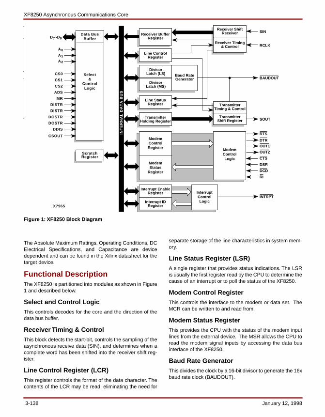
XF8250 Asynchronous Communications Core
The Absolute Maximum Ratings, Operating Conditions, DCElectrical Specifications, and Capacitance are devicedependent and can be found in the Xilinx datasheet for thetarget device.
Functional DescriptionThe XF8250 is partitioned into modules as shown in Figure1 and described below.
Select and Control Logic This controls decodes for the core and the direction of thedata bus buffer.
Receiver Timing & Control This block detects the start-bit, controls the sampling of theasynchronous receive data (SIN), and determines when acomplete word has been shifted into the receiver shift reg-ister.
Line Control Register (LCR) This register controls the format of the data character. Thecontents of the LCR may be read, eliminating the need for
separate storage of the line characteristics in system mem-ory.
Line Status Register (LSR) A single register that provides status indications. The LSRis usually the first register read by the CPU to determine thecause of an interrupt or to poll the status of the XF8250.
Modem Control Register This controls the interface to the modem or data set. TheMCR can be written to and read from.
Modem Status Register This provides the CPU with the status of the modem inputlines from the external device. The MSR allows the CPU toread the modem signal inputs by accessing the data businterface of the XF8250.
Baud Rate Generator This divides the clock by a 16-bit divisor to generate the 16xbaud rate clock (BAUDOUT).
Entry/Verification ViewLogicPROcap-
ture 6.1 orWorkView
OfficeSupport
AllianceCORE ™ Facts
Memec Design Services warrants that the design deliv-ered by Memec Design Services will conform to the design specification. This warranty expires 3 months from the date of delivery of the design database. Contact Memec Design Services for the Design License Agreement with complete “Terms and Conditions of Sale.”Notes:1. Assuming all core signals are routed off-chip.2. Minimum guaranteed speed to meet Harris specification.3. Specific devices are minimum size and speed recommended -
the core will work in larger or faster devices from the same fam-ilies.
Receiver ShiftReceiver
Receiver Timing& Control
TransmitterTiming & Control
TransmitterShift Register
Receiver BufferRegister
X7965
A
A
CS0
CS1
CS2
ADS
MR
DISTR
DISTR
DOSTR
DOSTR
DDIS
CSOUT
D -D7 0
0
1
A2
Select&
ControlLogic
ScratchRegister
Data BusBuffer
Line ControlRegister
INT
ER
NA
L D
AT
A B
US
Line StatusRegister
SOUT
INTRPT
BAUDOUT
SIN
RTS
DTR
OUT1
OUT2
CTS
DSR
DCD
RI
ModemControlRegister
ModemStatus
Register
DivisorLatch (LS)
DivisorLatch (MS)
Baud RateGenerator
RCLK
TransmitterHolding Register
Interrupt EnableRegister
Interrupt IDRegister
InterruptControlLogic
ModemControlLogic
Figure 1: XF8250 Block Diagram
3-138 January 12, 1998

Memec Design Services
Receiver Shift Register This register is programmable for 5, 6, 7, or 8 data-bits percharacter.
Transmitter Holding Register This register holds parallel data from the data bus (D0-D7)until the Transmitter Shift Register is empty and ready toaccept a new character for transmission.
Scratch Register This register is an 8-bit Read/Write register which has noeffect on the XF8250. It is intended as a scratch pad regis-ter to be used by the programmer to hold temporary data.
Interrupt ID Register This register provides the XF8250 with interrupt capabilityfor interfacing to microprocessors. In order to minimizesoftware overhead during data character transfers, theXF8250 four levels of interrupt priorities:
• Priority 1 - Receiver Line Status • Priority 2 - Received Data Ready • Priority 3 - Transmitter Holding Register Empty • Priority 4 - Modem Status
Interrupt Enable Register This is a Write register used to independently enable thefour XF8250 interrupts which activate the interrupt(INTRPT) output.
Core Modifications The XF8250 meets or exceeds the AC Specifications of theHarris 82C50A-5. However, in most cases the TimeSpecscan be tightened significantly. Successful operation with120 ns bus cycles has been achieved. In all cases, a post-route timing analysis should be performed to verify perfor-mance. Implementation beyond 10 MHz and other custom-izing is available through Memec Design Services.
Pinout The XF8250 may be implemented as stand-alone logicusing the provided pinout or may be implemented internallywith the user’s design. Both versions are included with theCore deliverables. Signal names are provided in the blockdiagram shown in Figure 1, and Table 1.
Core Assumptions Deviations from the Harris 82C50 functional specificationare described below. Memec Design Services will performany of the listed modifications upon request.
Table 1: Core Signal Pinout
Stop-Bit Programming When the UART is programmed for two stop-bits (1.5 in 5-bit mode), the receiver does not check for the second stop-bit. If the first stop-bit is high and the second stop-bit iseither high or low, the receiver moves the shift register con-tents into the
Receiver Buffer Register without posting a framing error. Inthe majority of applications, this will not cause a problem.However, in cases where a corrupted second stop-bit mustbe reported as a framing error, the receiver will need modi-fication.
External Crystal Support This core does not support connection of a crystal directlyto the device. The XC4000 and XC5200 families willrequire a clock input.
SignalSignal
DirectionDescription
D7-D0 In/Out Data bits 7-0A0 Input Register Reset 0A1 Input Register Reset 1A2 Input Register Reset 2CS0 Input Chip Select 0CS1 Input Chip Select 1/CS2 Input Chip Select 2/ADS Input Address StrobeMR Input Master ResetDISTR Input Data In Strobe/DISTR Input Data In StrobeDOSTR Input Data Out Strobe/DOSTR Input Data Out StrobeDDIS Output Driver DisableCSOUT Output Chip Select OutSIN Input Serial Data InputRCLK Input 16x Baud for Receiver/BAUDOUT Output BAUDOUTSOUT Output Serial Data Output/RTS Output Request to Send/DTR Output Data Terminal Ready/OUT1 Output Output 1/OUT2 Output Output 2/CTS Input Clear To Send/DSR Input Data Set Ready/DCD Input Data Carrier Detect/RI Input Ring IndicatorINTRPT Output Interrupt Requests
January 12, 1998 3-139
XF8250 Asynchronous Communications Core
Internal Loopback The internal loopback function (enabled by setting MCR(4))loops the four lower bits of the Modem Control Register(MCR) to the four upper bits of the Modem Status Register(MSR), however, the Harris 82C50A data sheet is ambigu-ous as to which MCR bit loops to which MSR bit. TheXF8250 Core loops these bits as follows:
MCR(0) (DTR) ----> MSR(5) (DSR)
MCR(1) (RTS) ----> MSR(4) (CTS)
MCR(2) (OUT1) ----> MSR(6) (RI)
MCR(3) (OUT2) ----> MSR(7) (DCD)
If it is discovered that this is incorrect, the design will needmodification.
Baud Rate Generator The Baud Rate Generator differs from the Harris datasheetin the following ways.
Divide by Zero - A divisor value of 0x0000 acts like divideby 65536, where “BAUDOUT” is high for one “XINCLK”period and low for 65535 “XINCLK” periods. The Harrisdatasheet does not specify what results from a divisor ofzero.
Divide by One - A divisor of one is not supported. The“BAUDOUT” signal is always high when a divisor of 0x0001is used. If only a divisor of one is required, “XINCLK” canbe connected directly to “RCLK” and “TXCLK” and theBaud Rate Generator can be removed entirely. If variousdivisors are required including divide by one, then the BaudRate Generator will have to be modified.
Other Division - For all divisor values between 0x0002 and0xffff, the “BAUDOUT” signal is high for one “XINCLK”period and low for N-1 “XINCLK” periods, where N is thedivisor value. For divisors of 0x0002 and 0x0003, the“BAUDOUT” signal is identical to the Harris datasheet.
For divisors greater than 0x0003, the Harris BAUDOUT sig-nal is high for two XTAL1 clock periods and low for N-2XTAL1 clock periods. The duty cycle is not an issue withinthe XF8250 macro, but external devices that use “BAUD-OUT” must consider this.
Verification Methods Complete functional and timing simulation has been per-formed on the XF8250 using ViewSim. (Simulation vectorsused for verification are provided with the core.) This corehas also been used successfully in customer designs. TheREADME.TXT file has a short description of three top levelCMD files used to simulate the design. These CMD files
call other CMD files (19 in all) and all the CMD files havedescriptions and comments as to their purpose.
Recommended Design Experience Users should be familiar with ViewLogic PROcapture orOffice schematic entry and Xilinx design flows. Usersshould also have experience with microprocessor systemsand asynchronous communication controllers.
Ordering Information The XF8250 Asynchronous Communications Core is pro-vided under license from Memec Design Services for use inXilinx programmable logic devices and Xilinx HardWiregate arrays. Please contact Memec for pricing and moreinformation.
Information furnished by Memec Design Services isbelieved to be accurate and reliable. Memec Design Ser-vices reserves the right to change specifications detailed inthis data sheet at any time without notice, in order toimprove reliability, function or design, and assumes noresponsibility for any errors within this document. MemecDesign Services does not make any commitment to updatethis information.
Memec Design Services assumes no obligation to correctany errors contained herein or to advise any user of thistext of any correction, if such be made, nor does the Com-pany assume responsibility for the functioning of unde-scribed features or parameters.
Memec Design Services will not assume any liability for theaccuracy or correctness of any support or assistance pro-vided to a user.
Memec Design Services does not represent that productsdescribed herein are free from patent infringement or fromany other third-party right. No license is granted by implica-tion or otherwise under any patent or patent rights ofMemec Design Services.
Memec Design Services products are not intended for usein life support appliances, devices, or systems. Use of aMemec Design Services product in such application with-out the written consent of the appropriate Memec DesignServices officer is prohibited.
All trademarks, registered trademarks, or servicemarks areproperty of their respective owners.
Related InformationHarris Semiconductor’s Microprocessor Products for Com-mercial and Military Digital Applications, 1992.
3-140 January 12, 1998
Memec Design Services
Xilinx Programmable LogicFor information on Xilinx programmable logic or develop-ment system software, contact your local Xilinx sales office,or:
Xilinx, Inc.2100 Logic DriveSan Jose, CA 95124Phone: +1 408-559-7778Fax: +1 408-559-7114URL: www.xilinx.com
For general Xilinx literature, contact:
Phone: +1 800-231-3386 (inside the US)+1 408-879-5017 (outside the US)
E-mail: [email protected]
For AllianceCORETM specific information, contact:
Phone: +1 408-879-5381E-mail: [email protected]: www.xilinx.com/products/logicore/alliance/
tblpart.htm
January 12, 1998 3-141
XF8250 Asynchronous Communications Core
3-142 January 12, 1998
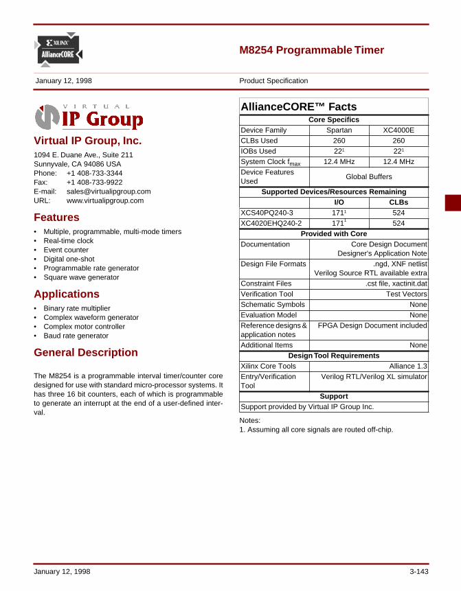
M8254 Programmable Timer
January 12, 1998 Product Specification
Virtual IP Group, Inc.1094 E. Duane Ave., Suite 211 Sunnyvale, CA 94086 USAPhone: +1 408-733-3344Fax: +1 408-733-9922E-mail: [email protected]: www.virtualipgroup.com
Features• Multiple, programmable, multi-mode timers• Real-time clock• Event counter• Digital one-shot• Programmable rate generator• Square wave generator
Applications• Binary rate multiplier• Complex waveform generator• Complex motor controller• Baud rate generator
General Description
The M8254 is a programmable interval timer/counter coredesigned for use with standard micro-processor systems. Ithas three 16 bit counters, each of which is programmableto generate an interrupt at the end of a user-defined inter-val.
Notes:1. Assuming all core signals are routed off-chip.
AllianceCORE™ FactsCore Specifics
Device Family Spartan XC4000ECLBs Used 260 260IOBs Used 221 221
System Clock fmax 12.4 MHz 12.4 MHzDevice Features Used
Global Buffers
Supported Devices/Resources RemainingI/O CLBs
XCS40PQ240-3 1711 524XC4020EHQ240-2 171
1524
Provided with CoreDocumentation Core Design Document
Designer's Application NoteDesign File Formats .ngd, XNF netlist
Verilog Source RTL available extraConstraint Files .cst file, xactinit.datVerification Tool Test VectorsSchematic Symbols NoneEvaluation Model NoneReference designs & application notes
FPGA Design Document included
Additional Items NoneDesign Tool Requirements
Xilinx Core Tools Alliance 1.3Entry/Verification Tool
Verilog RTL/Verilog XL simulator
SupportSupport provided by Virtual IP Group Inc.
January 12, 1998 3-143
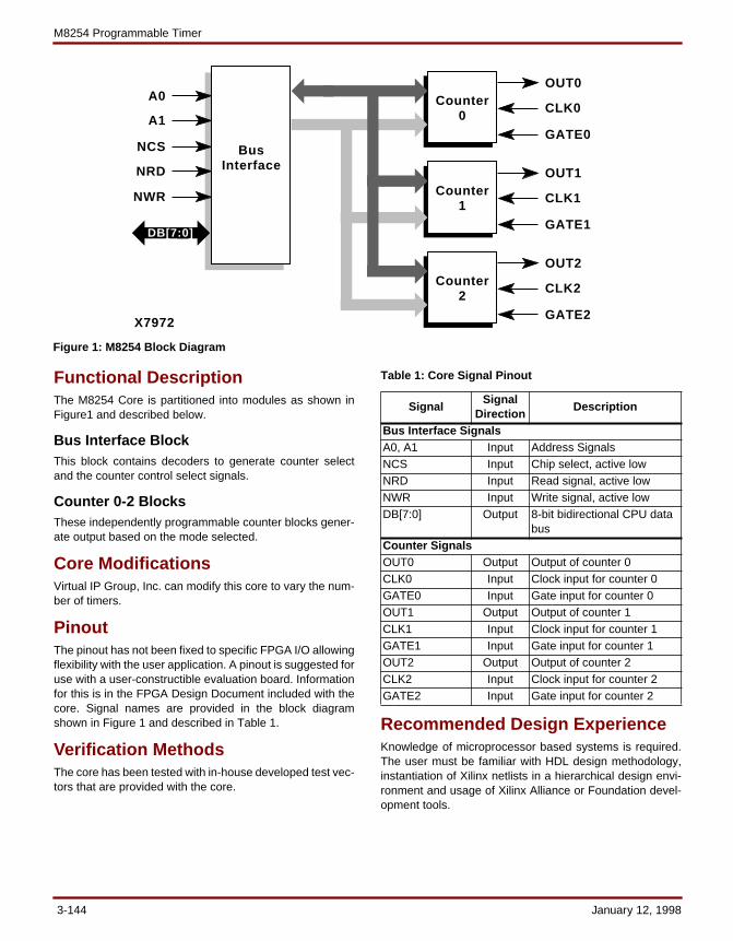
M8254 Programmable Timer
Functional DescriptionThe M8254 Core is partitioned into modules as shown inFigure1 and described below.
Bus Interface BlockThis block contains decoders to generate counter selectand the counter control select signals.
Counter 0-2 BlocksThese independently programmable counter blocks gener-ate output based on the mode selected.
Core ModificationsVirtual IP Group, Inc. can modify this core to vary the num-ber of timers.
PinoutThe pinout has not been fixed to specific FPGA I/O allowingflexibility with the user application. A pinout is suggested foruse with a user-constructible evaluation board. Informationfor this is in the FPGA Design Document included with thecore. Signal names are provided in the block diagramshown in Figure 1 and described in Table 1.
Verification MethodsThe core has been tested with in-house developed test vec-tors that are provided with the core.
Table 1: Core Signal Pinout
Recommended Design ExperienceKnowledge of microprocessor based systems is required.The user must be familiar with HDL design methodology,instantiation of Xilinx netlists in a hierarchical design envi-ronment and usage of Xilinx Alliance or Foundation devel-opment tools.
SignalSignal
DirectionDescription
Bus Interface SignalsA0, A1 Input Address SignalsNCS Input Chip select, active lowNRD Input Read signal, active lowNWR Input Write signal, active lowDB[7:0] Output 8-bit bidirectional CPU data
busCounter SignalsOUT0 Output Output of counter 0CLK0 Input Clock input for counter 0GATE0 Input Gate input for counter 0OUT1 Output Output of counter 1CLK1 Input Clock input for counter 1GATE1 Input Gate input for counter 1OUT2 Output Output of counter 2CLK2 Input Clock input for counter 2GATE2 Input Gate input for counter 2
Counter0
X7972
A0OUT0
CLK0
GATE0
DB[7:0]
A1
NCS
NRD
NWR
BusInterface
Counter1
OUT1
CLK1
GATE1
Counter2
OUT2
CLK2
GATE2
Figure 1: M8254 Block Diagram
3-144 January 12, 1998
Virtual IP Group Inc.
Available Support Products
FPGA Evaluation BoardThe FPGA Design Document included with the core givesdirections for constructing a general purpose FPGA evalu-ation daughter board that can be plugged into a standardpart socket on the target system through a flat cable.
Ordering InformationThis product is available from Virtual IP Group, Inc. Pleasecontact them for pricing and additional information.
Related Information
Xilinx Programmable LogicFor information on Xilinx programmable logic or develop-ment system software, contact your local Xilinx sales office,
or:Xilinx, Inc.2100 Logic DriveSan Jose, CA 95124Phone: +1 408-559-7778Fax: +1 408-559-7114URL: www.xilinx.com
For general Xilinx literature, contact:
Phone: +1 800-231-3386 (inside the US)+1 408-879-5017 (outside the US)
E-mail: [email protected]
For AllianceCORE™ specific information, contact:
Phone: +1 408-879-5381E-mail: [email protected]: www.xilinx.com/products/logicore/alliance/
tblpart.htm
January 12, 1998 3-145
M8254 Programmable Timer
3-146 January 12, 1998
January 12, 1998 Product Specification
M8255 Programmable Peripheral Interface
Virtual IP Group, Inc.1094 E. Duane Ave., Suite 211Sunnyvale, CA 94086 USAPhone: +1 408-733-3344Fax: +1 408-733-9922E-mail: [email protected]: www.virtualipgroup.com
Features• Multi-mode programmable parallel I/O port peripheral
interface• 24 programmable general purpose I/O signals• Functionally compatible with Intel 8255A• Control word read-back facility• Direct bit set/reset capability• I/O data transfer with handshaking
Applications• General purpose I/O ports used to control external
peripherals
General DescriptionThe M8255 Programmable Peripheral Interface (PPI) coreis a general purpose I/O component to interface peripheralequipment to a microcomputer system bus. The functionalconfiguration of the M8255 is programmable. This core isfunctionally compatible with the INTEL 8255.
Notes:1. Assuming all core signals are routed off-chip.
AllianceCORE ™ FactsCore Specifics
Device Family Spartan XC4000ECLBs Used 111 111
IOBs Used 381
381
System Clock fmax 15.2 MHz 15.2 MHzDevice Features Used
Global Buffers
Supported Devices/Resources RemainingI/O CLBs
XCS40PQ240-3 1551 673
XC4020EHQ240-2 1551
673Provided with Core
Documentation Core Design DocumentDesigner's Application Note
Design File Formats .ngd, XNF netlistVerilog Source RTL available extra
Constraint Files .cst file, xactinit.datVerification Tool Test VectorsSchematic Symbols NoneEvaluation Model NoneReference designs & application notes
FPGA Design Document included
Additional Items NoneDesign Tool Requirements
Xilinx Core Tools Alliance 1.3Entry/Verification Tool
Verilog RTL/Verilog XL simulator
SupportSupport provided by Virtual IP Group, Inc.
January 12, 1998 3-147
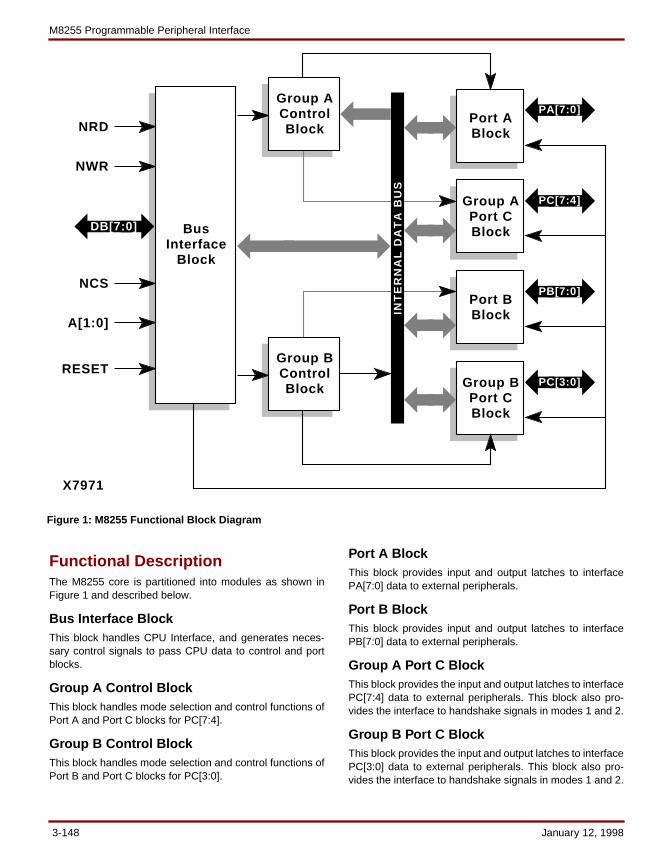
M8255 Programmable Peripheral Interface
Functional DescriptionThe M8255 core is partitioned into modules as shown inFigure 1 and described below.
Bus Interface Block This block handles CPU Interface, and generates neces-sary control signals to pass CPU data to control and portblocks.
Group A Control BlockThis block handles mode selection and control functions ofPort A and Port C blocks for PC[7:4].
Group B Control BlockThis block handles mode selection and control functions ofPort B and Port C blocks for PC[3:0].
Port A BlockThis block provides input and output latches to interfacePA[7:0] data to external peripherals.
Port B BlockThis block provides input and output latches to interfacePB[7:0] data to external peripherals.
Group A Port C BlockThis block provides the input and output latches to interfacePC[7:4] data to external peripherals. This block also pro-vides the interface to handshake signals in modes 1 and 2.
Group B Port C BlockThis block provides the input and output latches to interfacePC[3:0] data to external peripherals. This block also pro-vides the interface to handshake signals in modes 1 and 2.
Port ABlock
X7971
NRD
DB[7:0]
PA[7:0]
NWR
NCS
A[1:0]
RESET
BusInterface
Block
Group APort CBlock
Port BBlock
Group BPort CBlock
PC[7:4]
PB[7:0]
PC[3:0]IN
TE
RN
AL
DA
TA
BU
S
Group AControlBlock
Group BControlBlock
Figure 1: M8255 Functional Block Diagram
3-148 January 12, 1998
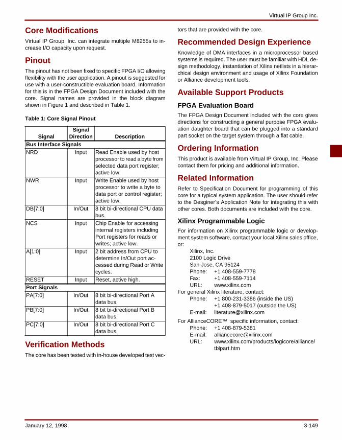
Virtual IP Group Inc.
Core ModificationsVirtual IP Group, Inc. can integrate multiple M8255s to in-crease I/O capacity upon request.
PinoutThe pinout has not been fixed to specific FPGA I/O allowingflexibility with the user application. A pinout is suggested foruse with a user-constructible evaluation board. Informationfor this is in the FPGA Design Document included with thecore. Signal names are provided in the block diagramshown in Figure 1 and described in Table 1.
Table 1: Core Signal Pinout
Verification MethodsThe core has been tested with in-house developed test vec-
tors that are provided with the core.
Recommended Design ExperienceKnowledge of DMA interfaces in a microprocessor basedsystems is required. The user must be familiar with HDL de-sign methodology, instantiation of Xilinx netlists in a hierar-chical design environment and usage of Xilinx Foundationor Alliance development tools.
Available Support Products
FPGA Evaluation BoardThe FPGA Design Document included with the core givesdirections for constructing a general purpose FPGA evalu-ation daughter board that can be plugged into a standardpart socket on the target system through a flat cable.
Ordering InformationThis product is available from Virtual IP Group, Inc. Pleasecontact them for pricing and additional information.
Related InformationRefer to Specification Document for programming of thiscore for a typical system application. The user should referto the Desginer’s Application Note for integrating this withother cores. Both documents are included with the core.
Xilinx Programmable LogicFor information on Xilinx programmable logic or develop-ment system software, contact your local Xilinx sales office,or:
Xilinx, Inc.2100 Logic DriveSan Jose, CA 95124Phone: +1 408-559-7778Fax: +1 408-559-7114URL: www.xilinx.com
For general Xilinx literature, contact:Phone: +1 800-231-3386 (inside the US)
+1 408-879-5017 (outside the US)E-mail: [email protected]
For AllianceCORE™ specific information, contact:Phone: +1 408-879-5381E-mail: [email protected]: www.xilinx.com/products/logicore/alliance/
tblpart.htm
SignalSignal
Direction DescriptionBus Interface SignalsNRD Input Read Enable used by host
processor to read a byte from selected data port register; active low.
NWR Input Write Enable used by host processor to write a byte to data port or control register; active low.
DB[7:0] In/Out 8 bit bi-directional CPU data bus.
NCS Input Chip Enable for accessing internal registers including Port registers for reads or writes; active low.
A[1:0] Input 2 bit address from CPU to determine In/Out port ac-cessed during Read or Write cycles.
RESET Input Reset, active high.Port SignalsPA[7:0] In/Out 8 bit bi-directional Port A
data bus.PB[7:0] In/Out 8 bit bi-directional Port B
data bus.PC[7:0] In/Out 8 bit bi-directional Port C
data bus.
January 12, 1998 3-149

M8255 Programmable Peripheral Interface
3-150 January 12, 1998
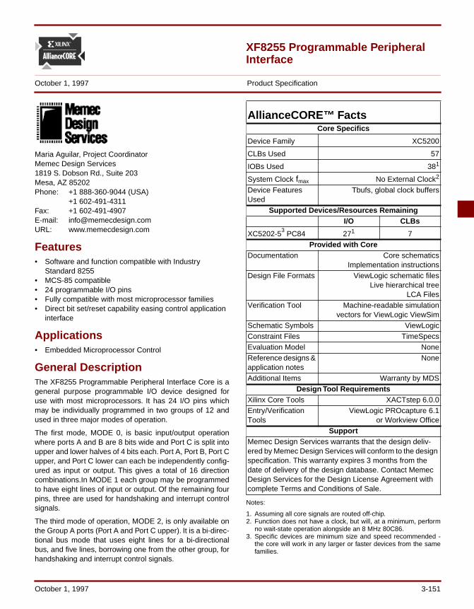
XF8255 Programmable Peripheral Interface
October 1, 1997 Product Specification
Maria Aguilar, Project Coordinator Memec Design Services1819 S. Dobson Rd., Suite 203Mesa, AZ 85202Phone: +1 888-360-9044 (USA)
+1 602-491-4311Fax: +1 602-491-4907E-mail: [email protected]: www.memecdesign.com
Features• Software and function compatible with Industry
Standard 8255• MCS-85 compatible• 24 programmable I/O pins• Fully compatible with most microprocessor families• Direct bit set/reset capability easing control application
interface
Applications• Embedded Microprocessor Control
General DescriptionThe XF8255 Programmable Peripheral Interface Core is ageneral purpose programmable I/O device designed foruse with most microprocessors. It has 24 I/O pins whichmay be individually programmed in two groups of 12 andused in three major modes of operation.
The first mode, MODE 0, is basic input/output operationwhere ports A and B are 8 bits wide and Port C is split intoupper and lower halves of 4 bits each. Port A, Port B, Port Cupper, and Port C lower can each be independently config-ured as input or output. This gives a total of 16 directioncombinations.In MODE 1 each group may be programmedto have eight lines of input or output. Of the remaining fourpins, three are used for handshaking and interrupt controlsignals.
The third mode of operation, MODE 2, is only available onthe Group A ports (Port A and Port C upper). It is a bi-direc-tional bus mode that uses eight lines for a bi-directionalbus, and five lines, borrowing one from the other group, forhandshaking and interrupt control signals.
Notes:
1. Assuming all core signals are routed off-chip.2. Function does not have a clock, but will, at a minimum, perform
no wait-state operation alongside an 8 MHz 80C86.3. Specific devices are minimum size and speed recommended -
the core will work in any larger or faster devices from the samefamilies.
AllianceCORE™ FactsCore Specifics
Device Family XC5200
CLBs Used 57
IOBs Used 381
System Clock fmax No External Clock2
Device Features Used
Tbufs, global clock buffers
Supported Devices/Resources RemainingI/O CLBs
XC5202-53 PC84 271 7Provided with Core
Documentation Core schematicsImplementation instructions
Design File Formats ViewLogic schematic filesLive hierarchical tree
LCA FilesVerification Tool Machine-readable simulation
vectors for ViewLogic ViewSimSchematic Symbols ViewLogicConstraint Files TimeSpecsEvaluation Model NoneReference designs & application notes
None
Additional Items Warranty by MDSDesign Tool Requirements
Xilinx Core Tools XACTstep 6.0.0Entry/Verification Tools
ViewLogic PROcapture 6.1or Workview Office
SupportMemec Design Services warrants that the design deliv-ered by Memec Design Services will conform to the design specification. This warranty expires 3 months from the date of delivery of the design database. Contact Memec Design Services for the Design License Agreement with complete Terms and Conditions of Sale.
October 1, 1997 3-151
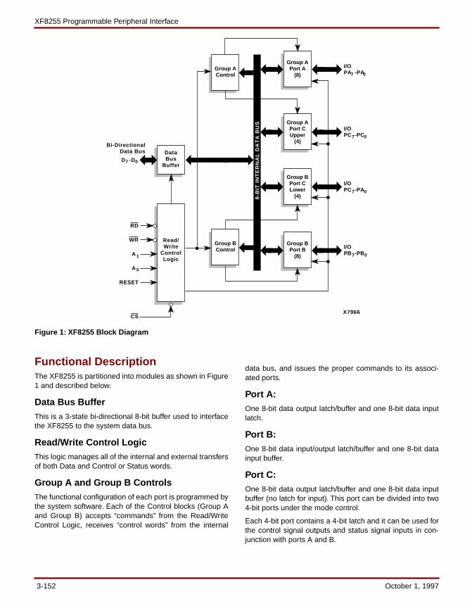
XF8255 Programmable Peripheral Interface
Functional DescriptionThe XF8255 is partitioned into modules as shown in Figure1 and described below.
Data Bus BufferThis is a 3-state bi-directional 8-bit buffer used to interfacethe XF8255 to the system data bus.
Read/Write Control LogicThis logic manages all of the internal and external transfersof both Data and Control or Status words.
Group A and Group B ControlsThe functional configuration of each port is programmed bythe system software. Each of the Control blocks (Group Aand Group B) accepts “commands” from the Read/WriteControl Logic, receives “control words” from the internal
data bus, and issues the proper commands to its associ-ated ports.
Port A: One 8-bit data output latch/buffer and one 8-bit data inputlatch.
Port B:One 8-bit data input/output latch/buffer and one 8-bit datainput buffer.
Port C: One 8-bit data output latch/buffer and one 8-bit data inputbuffer (no latch for input). This port can be divided into two4-bit ports under the mode control.
Each 4-bit port contains a 4-bit latch and it can be used forthe control signal outputs and status signal inputs in con-junction with ports A and B.
Group APort A
(8)
I/OPA -PA
Group AControl
X7966
RD
WR
A 1
0A
RESET
CS
D -D7 0
Read/Write
ControlLogic
DataBus
Buffer
Bi-DirectionalData Bus
Group APort CUpper
(4)
Group BPort CLower
(4)
Group BPort B
(8)
Group BControl
8-B
IT I
NT
ER
NA
L D
AT
A B
US
7 0
I/OPC -PC7 0
I/OPC -PA7 0
I/OPB -PB7 0
Figure 1: XF8255 Block Diagram
3-152 October 1, 1997
Memec Design Services
PinoutThe XF8255 may be implemented as stand-alone logicusing the provided pinout or may be implemented internallywith the users design. Both versions are included with theCore deliverables. Signal names are provided in the blockdiagram shown in Figure 1, and Table 1.
Core Assumptions Deviations from the Harris 82C55A functional specificationare described below. Memec Design Services will performany of the listed modifications upon request.
IBF Flip-flopsThe Input Buffer Full (IBF) flip-flops on ports A and B arenot cleared when RESET is asserted. This is because theXilinx architecture does not easily support D flip-flops withboth asynchronous Set and asynchronous Reset.
Workaround: Perform a dummy read of ports A and Bsometime after RESET is pulsed. This will clear the IBF flip-flops.
Input Side Interrupt Request Flip-flopsThe input side Interrupt Request (IN_INTR) flip-flops forPort A MODEs 1 and 2 and Port B MODE 1 are clearedasynchronously (level sensitive) when a read is performedon the port. The timing diagram (Figure 7) in the Harris82C55A data sheet agrees with our implementation, how-ever, the text in the data sheet says it is reset by the fallingedge of RD.
Workaround : Since the Harris data sheet is inconsistenton this point and since our XF8255 still meets all the timingrelationships indicated in Figure 7 of the Harris 82C55Adata sheet, this change should be transparent to the user.
The input side Interrupt Request (IN_INTR) flip-flops forPort A MODEs 1 and 2 and Port B MODE 1, are set on theRISING EDGE of STBx_L when IBFx, INTEx, andPx_RD_L are high. The Harris data sheet indicates that thisshould be LEVEL sensitive. Since the Xilinx architecturedoes not easily support flip-flops with both asynchronousSet and Asynchronous Reset, we chose to use the risingedge of STBx_L to set the flip-flop.
Workaround: Since our XF8255 still meets all the timingrelationships indicated in Figure 7 of the Harris 82C55Adata sheet, this change should be transparent to the user.
Output Side Interrupt Request Flip-flopsThe output side Interrupt Request (OUT_INTR) flip-flopsfor Port A MODEs 1 and 2 and Port B MODE 1, are clearedasynchronously (level sensitive) when a write is performedon the port. The timing diagram (Figure 9) in the Harris82C55A data sheet agrees with our implementation, how-ever, the text in the data sheet says it is reset by the fallingedge of WR.
Table 1: Core Signal Pinout
Workaround: Since the Harris data sheet is inconsistenton this point and since our XF8255 still meets all the timingrelationships indicated in Figure 9 of the Harris 82C55Adata sheet, this change should be transparent to the user.
The output side Interrupt Request (OUT_INTR) flip-flopsfor Port A MODEs 1 and 2 and Port B MODE 1, are set onthe RISING EDGE of ACKx_L when OBFx_L, INTEx, andPx_WR_L are high. The Harris data sheet indicates thatthis should be LEVEL sensitive. Since the Xilinx architec-ture does not easily support flip-flops with both asynchro-nous Set and asynchronous Reset, we chose to use therising edge of ACKx_L to set the flip-flop.
SignalSignal
Direction Description
Control SignalsRD- Input READ: used by the CPU to
read status information or data via the data bus; active low
WR- Input WRITE: used by the CPU to load control words and data into the 82C55A; active low
A0-A1 Input ADDRESS: used in conjunc-tion with RD- and WR- inputs to control selection of the control word register ports. A0 and A1 are normally con-nected to the least significant bits of address bus A0, A1
RESET Input RESET: A high on this input clears the control register and all ports (A,B,C) are set to input mode with “bus hold” circuitry turned on
CS- Input CHIP SELECT: used to en-able the 802C55A onto the data bus for CPU communi-cations; active low
Port and Data Bus Signals
D0-D7 In/Out DATA BUS: bidirectional three-state pins connected to system data bus
PA0-PA7 In/Out PORT A: 8-bit input and out-put port. Both bus hold high and bus hold low circuitry are present on this port
PB0-PB7 In/Out PORT B: 8-bit input and out-put port. Bus hold high cir-cuitry is present on this port
PC0-PC7 In/Out PORT C: 8-bit input and out-put port. Bus hold circuitry is present on this port
October 1, 1997 3-153
XF8255 Programmable Peripheral Interface
Workaround: Since our XF8255 still meets all the timingrelationships indicated in Figure 9 of the Harris 82C55Adata sheet, this change should be transparent to the user.
Bus-Hold CapabilityPorts A, B, and C do not have Bus-Hold capability. Thiswould require two OBUFTs per port pin. Since Xilinxdevices only have one OBUFT per pin, it would take two Xil-inx pins connected together externally for each port pin.
Workaround: Most applications don't require Bus-Holdcapability, but for those that do, a customized version of theXF8255 macro can be developed.
Core ModificationsThe XF8255 is designed to meet or exceed the AC Specifi-cations of the Harris 82C55A. However, in most cases theTimespecs can be tightened significantly. In all cases, apost-route timing analysis should be performed to verifyperformance. Implementation and other customizing isavailable through Memec Design Services.
Verification MethodsComplete functional and timing simulation has been per-formed on the XF8255 using Viewsim. (Simulation vectorsused for verification are provided with the core.) TheREADME.TXT file has a short description of four top levelCMD files used to simulate the design. These CMD filescall other CMD files and all the CMD files have descriptionsand comments as to their purpose.
Recommended Design ExperienceUsers should be familiar with ViewLogic PROcapture orOffice schematic entry and Xilinx design flows. Usersshould also have experience with microprocessor systems.
Ordering InformationThe XF8255 Programmable Peripheral Interface Core isprovided under license from Memec Design Services foruse in Xilinx programmable logic devices and Xilinx Hard-Wire gate arrays. Please contact the partner for pricingand more information.
Information furnished by Memec Design Services isbelieved to be accurate and reliable. Memec Design Ser-vices reserves the right to change specifications detailed inthis data sheet at any time without notice, in order toimprove reliability, function or design, and assumes noresponsibility for any errors within this document. Memec
Design Services does not make any commitment to updatethis information.
Memec Design Services assumes no obligation to correctany errors contained herein or to advise any user of thistext of any correction, if such be made, nor does the Com-pany assume responsibility for the functioning of unde-scribed features or parameters. Memec Design Serviceswill not assume any liability for the accuracy or correctnessof any support or assistance provided to a user.
Memec Design Services does not represent that productsdescribed herein are free from patent infringement or fromany other third-party right. No license is granted by implica-tion or otherwise under any patent or patent rights ofMemec Design Services.
Memec Design Services products are not intended for usein life support appliances, devices, or systems. Use of aMemec Design Services product in such application with-out the written consent of the appropriate Memec DesignServices officer is prohibited.
All trademarks, registered trademarks, or servicemarks areproperty of their respective owners.
Related InformationHarris Semiconductors 82C55A CMOS ProgrammablePeripheral Interface data sheet at: www.harris.com.
Xilinx Programmable LogicFor information on Xilinx programmable logic or develop-ment system software, contact your local Xilinx sales office,or:
Xilinx, Inc.2100 Logic DriveSan Jose, CA 95124Phone: +1 408-559-7778Fax: +1408-559-7114URL: www.xilinx.com
For general Xilinx literature, contact:
Phone: +1 800-231-3386 (inside the US)+1 408-879-5017 (outside the US)
E-mail: [email protected]
For AllianceCORETM
specific information, contact:
Phone: +1 408-879-5381 E-mail: [email protected]: www.xilinx.com/products/logicore
/alliance/tblpart.htm
3-154 October 1, 1997
October 20, 1997 Product Specification
XF8256 Multifunction Microprocessor Support Controller
Maria Aguilar, Project CoordinatorMemec Design Services1819 S. Dobson Rd., Suite 203Mesa, AZ 85202Phone: +1 888-360-9044 (USA)
+1 602-491-4311 (international)Fax: +1 602-491-4907E-mail: [email protected]: www.memecdesign.com
Features• Programmable serial asynchronous communications
interface for 5-, 6-, 7-, or 8-bit characters, 0.75, 1, 1.5, or 2 stop bits, and parity generation
• On-board baud rate generator programmable for 13 common baud rates up to 19.2 K bits/second, or an external baud clock maximum of 1M bit/second
• Five 8-bit programmable timer/counters; four can be cascaded to two 16-bit timer/counters
• Two 8-bit programmable parallel I/O ports; port 1 can be programmed for port 2 handshake controls and event counter input
• Eight-level priority interrupt controller programmable for 8085, 8086/88, 80186/188 systems and for fully nested interrupt capability
• Programmable system clock to 1x, 2x, 3x, or 5x 1.024 MHz
Applications• Serial communications• Process control• Embedded systems
AllianceCORE ™ FactsCore Specifics
Device Family XC4000E XC5200CLBs Used 137 64IOBs Used 381 381
System Clock fmax 10+ MHz2
Device Features Used
Tbufs, global clock buffers
Supported Devices/Resources RemainingI/O CLBs
XC4005E-43 PC84C 291 59
XC5202PC84-53 331 0Provided with Core
Documentation Core schematicsImplementation instructions
Design File Formats ViewLogic schematic filesLive hierarchical tree
LCA FilesConstraint Files NoneSchematic Symbols ViewLogicVerification Tool Machine-readable simulation
vectors for ViewLogic ViewSimEvaluation Model NoneReference designs & application notes
None
Additional Items Warranty by MDSDesign Tool Requirements
Xilinx Core Tools XACTstep 6.0.0Entry/Verification Tools
ViewLogic PROcapture 6.1or Workview Office
SupportMemec Design Services warrants that the design deliv-ered by Memec Design Services will conform to the design specification. This warranty expires 3 months from the date of delivery of the design database. Contact Memec Design Services for the Design License Agreement with complete Terms and Conditions of Sale.Notes:1. Assuming all core signals are routed off-chip.2. Minimum guaranteed speed.3. Specific devices are minimum size and speed recommended -
the core will work in any larger or faster devices from the samefamilies.
October 20, 1997 3-155
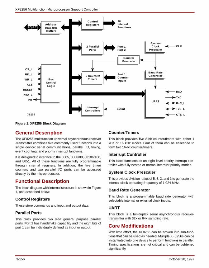
XF8256 Multifunction Microprocessor Support Controller
General DescriptionThe XF8256 multifunction universal asynchronous receiver-transmitter combines five commonly used functions into asingle device: serial communications, parallel I/O, timing,event counting, and priority interrupt functions.
It is designed to interface to the 8085, 8086/88, 80186/188,and 8051. All of these functions are fully programmablethrough internal registers. In addition, the five timer/counters and two parallel I/O ports can be accesseddirectly by the microprocessor.
Functional DescriptionThe block diagram with internal structure is shown in Figure1, and described below.
Control RegistersThese store commands and input and output data.
Parallel PortsThis block provides two 8-bit general purpose parallelports. Port 2 has handshake capability and the eight bits ofport 1 can be individually defined as input or output.
Counter/TimersThis block provides five 8-bit counter/timers with either 1kHz or 16 kHz clocks. Four of them can be cascaded toform two 16-bit counter/timers.
Interrupt ControllerThis block functions as an eight-level priority interrupt con-troller with fully nested or normal interrupt priority modes.
System Clock PrescalerThis provides division ratios of 5, 3, 2, and 1 to generate theinternal clock operating frequency of 1.024 MHz.
Baud Rate GeneratorThis block is a programmable baud rate generator withselectable internal or external clock inputs.
UARTThis block is a full-duplex serial asynchronous receiver-transmitter with 32x or 64x sampling rate.
Core ModificationsWith little effort, the XF8256 can be broken into sub-func-tions that can be used as needed. Multiple XF8256s can beinstantiated into one device to perform functions in parallel.Timing specifications are not critical and can be tightenedsignificantly.
Figure 1: XF8256 Block Diagram
X8258
ControlRegistersAddress/
Data BusBuffers
BusControlLogic
2 ParallelPorts
SystemClock
Prescaler
5 Counter/Timers
CounterPrescaler
Baud RateGenerator
UART
Port 1CounterInputs
CS_L
ToInternalFunctions
ExtintInterruptControllers
Port 1Port 2
CLK
RxD
TxD
RxC_L
TxC_L
CTS_L
RD_L
WR_L
ALE
RESET
INTA_L
INT
AD[0:7]
3-156 October 20, 1997
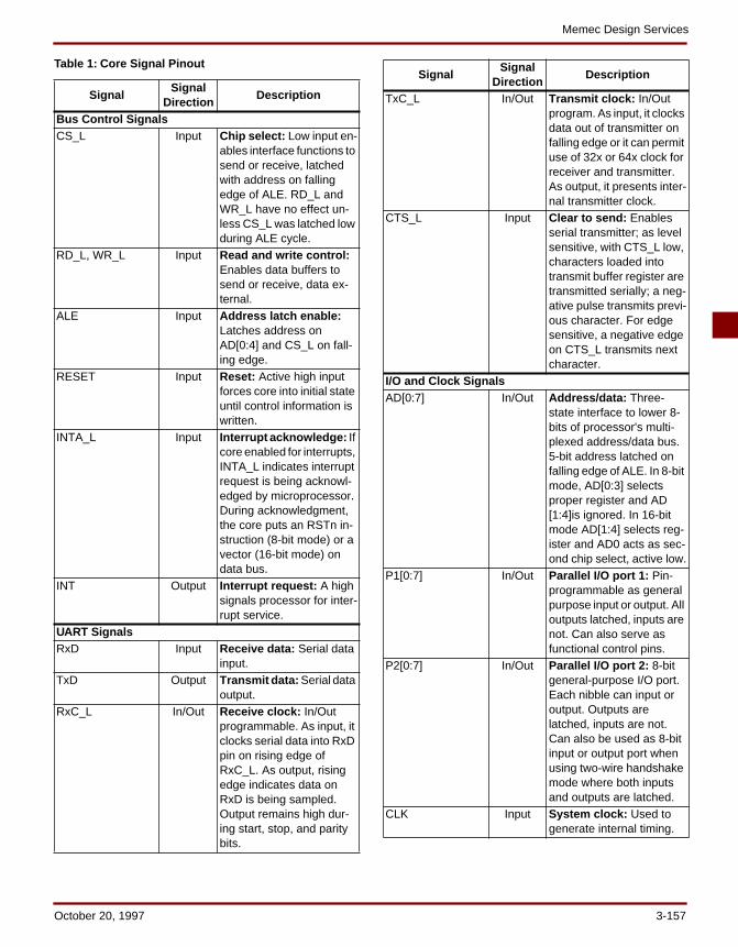
Memec Design Services
Table 1: Core Signal Pinout
SignalSignal
DirectionDescription
Bus Control SignalsCS_L Input Chip select: Low input en-
ables interface functions to send or receive, latched with address on falling edge of ALE. RD_L and WR_L have no effect un-less CS_L was latched low during ALE cycle.
RD_L, WR_L Input Read and write control: Enables data buffers to send or receive, data ex-ternal.
ALE Input Address latch enable: Latches address on AD[0:4] and CS_L on fall-ing edge.
RESET Input Reset: Active high input forces core into initial state until control information is written.
INTA_L Input Interrupt acknowledge: If core enabled for interrupts, INTA_L indicates interrupt request is being acknowl-edged by microprocessor. During acknowledgment, the core puts an RSTn in-struction (8-bit mode) or a vector (16-bit mode) on data bus.
INT Output Interrupt request: A high signals processor for inter-rupt service.
UART SignalsRxD Input Receive data: Serial data
input.TxD Output Transmit data: Serial data
output.RxC_L In/Out Receive clock: In/Out
programmable. As input, it clocks serial data into RxD pin on rising edge of RxC_L. As output, rising edge indicates data on RxD is being sampled. Output remains high dur-ing start, stop, and parity bits.
TxC_L In/Out Transmit clock: In/Out program. As input, it clocks data out of transmitter on falling edge or it can permit use of 32x or 64x clock for receiver and transmitter. As output, it presents inter-nal transmitter clock.
CTS_L Input Clear to send: Enables serial transmitter; as level sensitive, with CTS_L low, characters loaded into transmit buffer register are transmitted serially; a neg-ative pulse transmits previ-ous character. For edge sensitive, a negative edge on CTS_L transmits next character.
I/O and Clock SignalsAD[0:7] In/Out Address/data: Three-
state interface to lower 8-bits of processor's multi-plexed address/data bus. 5-bit address latched on falling edge of ALE. In 8-bit mode, AD[0:3] selects proper register and AD [1:4]is ignored. In 16-bit mode AD[1:4] selects reg-ister and AD0 acts as sec-ond chip select, active low.
P1[0:7] In/Out Parallel I/O port 1: Pin-programmable as general purpose input or output. All outputs latched, inputs are not. Can also serve as functional control pins.
P2[0:7] In/Out Parallel I/O port 2: 8-bit general-purpose I/O port. Each nibble can input or output. Outputs are latched, inputs are not. Can also be used as 8-bit input or output port when using two-wire handshake mode where both inputs and outputs are latched.
CLK Input System clock: Used to generate internal timing.
SignalSignal
DirectionDescription
October 20, 1997 3-157
XF8256 Multifunction Microprocessor Support Controller
In all cases, a functional and post-route timing analysisshould be performed to verify performance. Implementationand customizing is available through Memec Design Ser-vices.
PinoutThe XF8256 may be implemented internally with the user’sdesign or as stand-alone logic with the pinout that is pro-vided with the Core. For a fast replacement of the industrystandard 8256, MDS offers a 40-pin device carrier that ispin-compatible. Signal names are provided in the block dia-gram shown in Figure 1 and described in Table 1.
Verification MethodsBasic functional simulation has been performed on theXF8256 using ViewSim. Simulation vectors used for verifi-cation are provided with the core. This FPGA design wasalso physically tested and compared with the industry stan-dard 8256 for verification purposes.
Additional Support ProductsMemec Design Services supplies a Xilinx-based FPGADevelopment Module that can be used to hardware test thisand other MDS cores. To purchase this, or obtain moreinformation, contact MDS directly.
Recommended Design ExperienceUsers should be familiar with ViewLogic PRO series orWorkview Office schematic entry and Xilinx design flows.Users should also have experience with microprocessorsystems.
Ordering InformationThe XF8256 Multifunction Microprocessor Support Con-troller is provided under license from Memec Design Ser-vices for use in Xilinx programmable logic devices andXilinx HardWireTM gate arrays. To purchase or make furtherinquiries about this or other Memec Design Services prod-ucts, contact MDS directly at the location listed on the frontpage.
Information furnished by Memec Design Services isbelieved to be accurate and reliable. Memec Design Ser-
vices reserves the right to change specifications detailed inthis data sheet at any time without notice, in order toimprove reliability, function or design, and assumes noresponsibility for any errors within this document. MemecDesign Services does not make any commitment to updatethis information.
Memec Design Services assumes no obligation to correctany errors contained herein or to advise any user of thistext of any correction, if such be made, nor does the Com-pany assume responsibility for the functioning of unde-scribed features or parameters. Memec Design Serviceswill not assume any liability for the accuracy or correctnessof any support or assistance provided to a user.
Memec Design Services does not represent that productsdescribed herein are free from patent infringement or fromany other third-party right. No license is granted by implica-tion or otherwise under any patent or patent rights ofMemec Design Services.
Memec Design Services products are not intended for usein life support appliances, devices, or systems. Use of aMemec Design Services product in such application with-out the written consent of the appropriate Memec DesignServices officer is prohibited.
All trademarks, registered trademarks, or servicemarks areproperty of their respective owners.
Related Documentation and InformationIntel 8256AH Multifunction Microprocessor Support Con-troller, data sheet, 1994, order number 230759-002.
Xilinx Programmable LogicFor information on Xilinx programmable logic or develop-ment system software, contact your local Xilinx sales office,or:
Xilinx, Inc.2100 Logic DriveSan Jose, CA 95124Phone: +1 408-559-7778Fax: +1 408-559-7114URL: www.xilinx.com
For general Xilinx literature, contact:
Phone: +1 800-231-3386 (inside the US)+1 408-879-5017 (outside the US)
E-mail: [email protected]
For AllianceCORE™
specific information, contact:
Phone: +1 408-879-5381 E-mail: [email protected]: www.xilinx.com/products
/logicore/alliance/tblpart.htm
Table 1: Core Signal Pinout (cont.)
SignalSignal
DirectionDescription
EXTINT Input External interrupt re-quest: Input is level-high sensitive; must be held high until an interrupt ac-knowledge occurs.
3-158 October 20, 1997
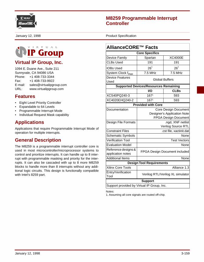
January 12, 1998 Product Specification
M8259 Programmable Interrupt Controller
Virtual IP Group, Inc.1094 E. Duane Ave., Suite 211Sunnyvale, CA 94086 USAPhone: +1 408-733-3344Fax: +1 408-733-9922E-mail: [email protected]: www.virtualipgroup.com
Features• Eight Level Priority Controller• Expandable to 64 Levels• Programmable Interrupt Mode• Individual Request Mask capability
ApplicationsApplications that require Programmable Interrupt Mode ofoperation for multiple interrupts.
General DescriptionThe M8259 is a programmable interrupt controller core isused in most microcontroller/microprocessor systems tocontrol and prioritize interrupts. It can handle up to 8 inter-rupt with programmable masking and priority for the inter-rupts. It can also be cascaded with up to 8 more M8259blocks to handle more than 8 interrupts without any addi-tional logic circuits. This design is functionally compatiblewith Intel’s 8259 part.
Notes:1. Assuming all core signals are routed off-chip.
AllianceCORE™ FactsCore Specifics
Device Family Spartan XC4000ECLBs Used 191 191
IOBs Used 261
261
System Clock fmax 7.5 MHz 7.5 MHz Device Features Used
Global Buffers
Supported Devices/Resources RemainingI/O CLBs
XCS40PQ240-3 1671 593XC4020EHQ240-2 1671 593
Provided with CoreDocumentation Core Design Document
Designer's Application NoteFPGA Design Document
Design File Formats .ngd, XNF netlistVerilog Source RTL
Constraint Files .cst file, xactinit.datSchematic Symbols NoneVerification Tool Test VectorsEvaluation Model NoneReference designs & application notes
FPGA Design Document included
Additional Items NoneDesign Tool Requirements
Xilinx Core Tools Alliance 1.3Entry/Verification Tool
Verilog RTL/Verilog XL simulator
SupportSupport provided by Virtual IP Group, Inc.
January 12, 1998 3-159
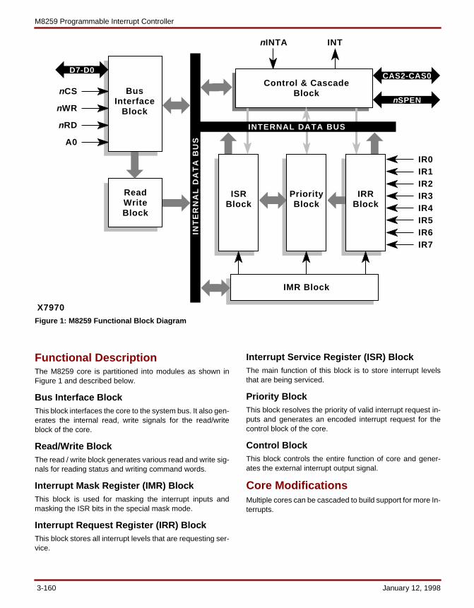
M8259 Programmable Interrupt Controller
Functional DescriptionThe M8259 core is partitioned into modules as shown inFigure 1 and described below.
Bus Interface Block This block interfaces the core to the system bus. It also gen-erates the internal read, write signals for the read/writeblock of the core.
Read/Write BlockThe read / write block generates various read and write sig-nals for reading status and writing command words.
Interrupt Mask Register (IMR) BlockThis block is used for masking the interrupt inputs andmasking the ISR bits in the special mask mode.
Interrupt Request Register (IRR) BlockThis block stores all interrupt levels that are requesting ser-vice.
Interrupt Service Register (ISR) BlockThe main function of this block is to store interrupt levelsthat are being serviced.
Priority BlockThis block resolves the priority of valid interrupt request in-puts and generates an encoded interrupt request for thecontrol block of the core.
Control BlockThis block controls the entire function of core and gener-ates the external interrupt output signal.
Core ModificationsMultiple cores can be cascaded to build support for more In-terrupts.
Figure 1: M8259 Functional Block Diagram
ReadWriteBlock
ISRBlock
Control & CascadeBlock
IMR Block
X7970
nCS
nINTA INT
IR0
D7-D0CAS2-CAS0
nSPENnWR
nRD
A0
BusInterface
Block
PriorityBlock
IRRBlock
IR1IR2IR3IR4IR5IR6IR7
INTERNAL DATA BUS
INT
ER
NA
L D
AT
A B
US
3-160 January 12, 1998
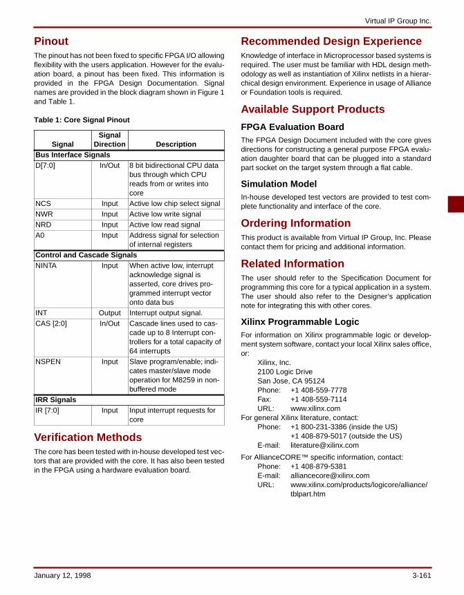
Virtual IP Group Inc.
PinoutThe pinout has not been fixed to specific FPGA I/O allowingflexibility with the users application. However for the evalu-ation board, a pinout has been fixed. This information isprovided in the FPGA Design Documentation. Signalnames are provided in the block diagram shown in Figure 1and Table 1.
Table 1: Core Signal Pinout
Verification MethodsThe core has been tested with in-house developed test vec-tors that are provided with the core. It has also been testedin the FPGA using a hardware evaluation board.
Recommended Design ExperienceKnowledge of interface in Microprocessor based systems isrequired. The user must be familiar with HDL design meth-odology as well as instantiation of Xilinx netlists in a hierar-chical design environment. Experience in usage of Allianceor Foundation tools is required.
Available Support Products
FPGA Evaluation Board The FPGA Design Document included with the core givesdirections for constructing a general purpose FPGA evalu-ation daughter board that can be plugged into a standardpart socket on the target system through a flat cable.
Simulation ModelIn-house developed test vectors are provided to test com-plete functionality and interface of the core.
Ordering InformationThis product is available from Virtual IP Group, Inc. Pleasecontact them for pricing and additional information.
Related InformationThe user should refer to the Specification Document forprogramming this core for a typical application in a system.The user should also refer to the Designer’s applicationnote for integrating this with other cores.
Xilinx Programmable LogicFor information on Xilinx programmable logic or develop-ment system software, contact your local Xilinx sales office,or:
Xilinx, Inc.2100 Logic DriveSan Jose, CA 95124Phone: +1 408-559-7778Fax: +1 408-559-7114URL: www.xilinx.com
For general Xilinx literature, contact:Phone: +1 800-231-3386 (inside the US)
+1 408-879-5017 (outside the US)E-mail: [email protected]
For AllianceCORE™ specific information, contact:Phone: +1 408-879-5381E-mail: [email protected]: www.xilinx.com/products/logicore/alliance/
tblpart.htm
SignalSignal
Direction DescriptionBus Interface SignalsD[7:0] In/Out 8 bit bidirectional CPU data
bus through which CPU reads from or writes into core
NCS Input Active low chip select signalNWR Input Active low write signalNRD Input Active low read signalA0 Input Address signal for selection
of internal registersControl and Cascade SignalsNINTA Input When active low, interrupt
acknowledge signal is asserted, core drives pro-grammed interrupt vector onto data bus
INT Output Interrupt output signal.CAS [2:0] In/Out Cascade lines used to cas-
cade up to 8 Interrupt con-trollers for a total capacity of 64 interrupts
NSPEN Input Slave program/enable; indi-cates master/slave mode operation for M8259 in non-buffered mode
IRR SignalsIR [7:0] Input Input interrupt requests for
core
January 12, 1998 3-161

M8259 Programmable Interrupt Controller
3-162 January 12, 1998
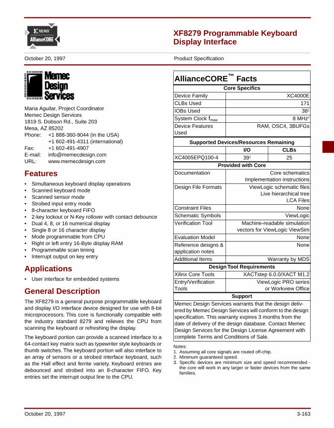
October 20, 1997 Product Specification
XF8279 Programmable Keyboard Display Interface
Maria Aguilar, Project CoordinatorMemec Design Services1819 S. Dobson Rd., Suite 203Mesa, AZ 85202Phone: +1 888-360-9044 (in the USA)
+1 602-491-4311 (international)Fax: +1 602-491-4907E-mail: [email protected]: www.memecdesign.com
Features• Simultaneous keyboard display operations• Scanned keyboard mode• Scanned sensor mode• Strobed input entry mode• 8-character keyboard FIFO• 2-key lockout or N-Key rollover with contact debounce• Dual 4, 8, or 16 numerical display• Single 8 or 16 character display• Mode programmable from CPU• Right or left entry 16-Byte display RAM• Programmable scan timing• Interrupt output on key entry
Applications• User interface for embedded systems
General DescriptionThe XF8279 is a general purpose programmable keyboardand display I/O interface device designed for use with 8-bitmicroprocessors. This core is functionally compatible withthe industry standard 8279 and relieves the CPU fromscanning the keyboard or refreshing the display.
The keyboard portion can provide a scanned interface to a64-contact key matrix such as typewriter style keyboards orthumb switches. The keyboard portion will also interface toan array of sensors or a strobed interface keyboard, suchas the Hall effect and ferrite variety. Keyboard entries aredebounced and strobed into an 8-character FIFO. Keyentries set the interrupt output line to the CPU.
Notes:1. Assuming all core signals are routed off-chip.2. Minimum guaranteed speed.3. Specific devices are minimum size and speed recommended -
the core will work in any larger or faster devices from the samefamilies.
AllianceCORE ™ FactsCore Specifics
Device Family XC4000ECLBs Used 171IOBs Used 381
System Clock fmax 8 MHz2
Device Features Used
RAM, OSC4, 3BUFGs
Supported Devices/Resources RemainingI/O CLBs
XC4005EPQ100-4 391 25Provided with Core
Documentation Core schematicsImplementation instructions
Design File Formats ViewLogic schematic filesLive hierarchical tree
LCA FilesConstraint Files NoneSchematic Symbols ViewLogicVerification Tool Machine-readable simulation
vectors for ViewLogic ViewSimEvaluation Model NoneReference designs & application notes
None
Additional Items Warranty by MDSDesign Tool Requirements
Xilinx Core Tools XACTstep 6.0.0/XACT M1.2Entry/Verification Tools
ViewLogic PRO seriesor Workview Office
SupportMemec Design Services warrants that the design deliv-ered by Memec Design Services will conform to the design specification. This warranty expires 3 months from the date of delivery of the design database. Contact Memec Design Services for the Design License Agreement with complete Terms and Conditions of Sale.
October 20, 1997 3-163
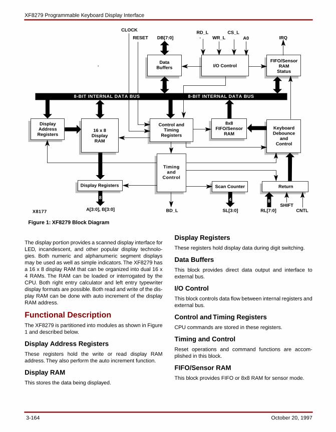
XF8279 Programmable Keyboard Display Interface
The display portion provides a scanned display interface forLED, incandescent, and other popular display technolo-gies. Both numeric and alphanumeric segment displaysmay be used as well as simple indicators. The XF8279 hasa 16 x 8 display RAM that can be organized into dual 16 x4 RAMs. The RAM can be loaded or interrogated by theCPU. Both right entry calculator and left entry typewriterdisplay formats are possible. Both read and write of the dis-play RAM can be done with auto increment of the displayRAM address.
Functional DescriptionThe XF8279 is partitioned into modules as shown in Figure1 and described below.
Display Address RegistersThese registers hold the write or read display RAMaddress. They also perform the auto increment function.
Display RAMThis stores the data being displayed.
Display RegistersThese registers hold display data during digit switching.
Data BuffersThis block provides direct data output and interface toexternal bus.
I/O ControlThis block controls data flow between internal registers andexternal bus.
Control and Timing RegistersCPU commands are stored in these registers.
Timing and ControlReset operations and command functions are accom-plished in this block.
FIFO/Sensor RAMThis block provides FIFO or 8x8 RAM for sensor mode.
X8177
Timingand
Control
KeyboardDebounce
andControl
FIFO/SensorRAM
Status
DisplayAddressRegisters
I/O Control
IRQ
DataBuffers
8x8FIFO/Sensor
RAM
Control andTiming
Registers16 x 8
DisplayRAM
Return
SL[3:0] RL[7:0]SHIFT
CNTLBD_L
Scan Counter
A0CS_L
WR_LRD_L
DB[7:0]RESET
CLOCK
A[3:0], B[3:0]
Display Registers
8-BIT INTERNAL DATA BUS 8-BIT INTERNAL DATA BUS
8 4 8
Figure 1: XF8279 Block Diagram
3-164 October 20, 1997

Memec Design Services
Table 1: Core Signal Pinout
Scan CounterThis counter has two modes. In encoded mode, the scancounter needs an external decoder to provide the scanlines for the keyboard and display. In decoded mode, thescan counter provides a decoded output, however, the key-board matrix is reduced to 4x8 and only 4 characters canbe displayed.
FIFO/Sensor RAM Status This block keeps track of how many characters are in theFIFO and provides flags for different functional conditions.
Keyboard Debounce and ControlIn keyboard mode, this block debounces the return lines. Insensor and strobed modes, data is directed and transferreddirectly to the FIFO/Sensor RAM.
ReturnThis block buffers and registers data from the Return, Con-trol, and Shift input lines.
Core ModificationsThe XF8279 is designed to meet or exceed the AC Specifi-cations of the Intel 8279. However, in most cases theTimespecs can be tightened significantly. In all cases, apost route timing analysis should be performed to verifyperformance. Implementation and customizing are avail-able through Memec Design Services.
PinoutThe XF8279 may be implemented internally with the user’sdesign or as stand alone logic with the pinout that is pro-vided with the Core. For a fast replacement of the industrystandard 8279 we provide a 40-pin device carrier which ispin compatible. Signal names are provided in the block dia-gram shown in Figure 1 and in Table 1.
Core Assumptions There is an important deviation in the design implementa-tion. The internal timing is fixed to 8 MHz (using OSC4) andonly the scan frequency is controlled by the external clock.The scan frequency is then synchronized with the internalclock. The reason for this is to meet and exceed the readand write cycle time. However, to our best understandingand practical experience, there are no deviations from the
SignalSignal
DirectionDescription
CLOCK Input Clock: Clock from system used to set scan frequency.
RESET Input Reset: A high input resets the XF8279.
DB[7:0] In/Out Bi-directional data bus: Three-state data and com-mand bus between CPU and XF8279.
RD_L, WR_L Input I/O Read and Write: En-ables data buffers to send or receive data from external bus.
CS-L Input Chip Select: A low input en-ables interface functions to read or write.
A0 Input Buffer Address: A high in-put indicates signals are in-terpreted as a command or status; a low indicates they are data.
IRQ Output Interrupt Request: In key-board mode, IRQ is high when data is in FIFO/Sensor RAM. In sensor mode, inter-rupt line goes high whenever a sensor change is detected.
A[3:0]B[3:0]
Output Outputs: Two data outputs for 16X4 display; ports may be blanked independently.
BD-L Output Blank Display: Output blanks display during digit switching or can be set by a display blanking command.
SL[3:0] Output Scan Lines: Used to scan key switch or sensor matrix and display digits; can be ei-ther encoded (1 of 16) or de-coded (1 of 4).
RL[7:0] Input Return Line: Inputs con-nected to scan lines through keys or sensor switches; in-ternal pull-up resistors keep them high until a switch clo-sure pulls one low.
Shift Input Shift: Shift-input status is stored along with key posi-tion on key closure in key-board modes; it has an inter-nal pull-up resistor.
CNTL Input Control/Strobed Input Mode: Status is stored on rising-edge; data into FIFO. It has an internal pull-up resis-tor.
SignalSignal
DirectionDescription
October 20, 1997 3-165
XF8279 Programmable Keyboard Display Interface
Intel 8279 functional specifications. Memec Design Ser-vices will perform any modification if a deviation is found.
Verification MethodsBasic functional simulation has been performed on theXF8279 using ViewSim. (Simulation vectors used for verifi-cation are provided with the core). The design was alsophysically tested in three different environments and twodifferent Xilinx FPGA devices without any problem.
Recommended Design ExperienceUsers should be familiar with ViewLogic PRO series orWorkview Office schematic entry and Xilinx design flows.Users should also have experience with microprocessorsystems.
Available Support ProductsMemec Design Services supplies a Xilinx-based FPGADevelopment Module that can be used to hardware test thisand other MDS cores. To purchase this, or obtain moreinformation, contact MDS directly.
Ordering InformationThe XF8259 Programmable Keyboard Display Interface isprovided under license from Memec Design Services foruse in Xilinx programmable logic devices and Xilinx Hard-WireTM gate arrays. To purchase or make further inquiriesabout this or other Memec Design Services products, con-tact MDS directly at the location listed on the front page.
Information furnished by Memec Design Services isbelieved to be accurate and reliable. Memec Design Ser-vices reserves the right to change specifications detailed inthis data sheet at any time without notice, in order toimprove reliability, function or design, and assumes noresponsibility for any errors within this document. MemecDesign Services does not make any commitment to updatethis information.
Memec Design Services assumes no obligation to correctany errors contained herein or to advise any user of thistext of any correction, if such be made, nor does the Com-pany assume responsibility for the functioning of unde-scribed features or parameters. Memec Design Services
will not assume any liability for the accuracy or correctnessof any support or assistance provided to a user.
Memec Design Services does not represent that productsdescribed herein are free from patent infringement or fromany other third party right. No license is granted by implica-tion or otherwise under any patent or patent rights ofMemec Design Services.
Memec Design Services products are not intended for usein life support appliances, devices, or systems. Use of aMemec Design Services product in such application with-out the written consent of the appropriate Memec DesignServices officer is prohibited.
All trademarks, registered trademarks, or servicemarks areproperty of their respective owners.
Related Documentation and InformationIntel 8279/8279-5 Programmable Keyboard/Display Inter-face, data sheet, 1993, order number 290123-002.
Xilinx Programmable LogicFor information on Xilinx programmable logic or develop-ment system software, contact your local Xilinx sales office,or:
Xilinx, Inc.2100 Logic DriveSan Jose, CA 95124Phone: +1 408-559-7778Fax: +1 408-559-7114URL: www.xilinx.com
For general Xilinx literature, contact:
Phone: +1 800-231-3386 (inside the US)+1 408-879-5017 (outside the US)
E-mail: [email protected]
For AllianceCORE™
specific information, contact:
Phone: +1 408-879-5381 E-mail: [email protected]: www.xilinx.com/products
/logicore/alliance/tblpart.htm
3-166 October 20, 1997
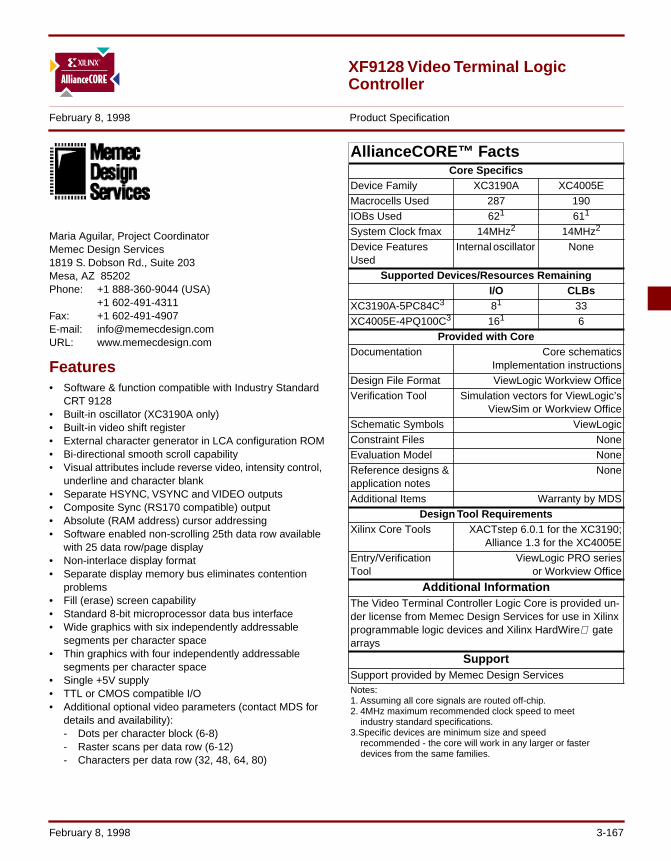
XF9128 Video Terminal Logic Controller
February 8, 1998 Product Specification
Maria Aguilar, Project Coordinator Memec Design Services 1819 S. Dobson Rd., Suite 203 Mesa, AZ 85202 Phone: +1 888-360-9044 (USA)
+1 602-491-4311Fax: +1 602-491-4907 E-mail: [email protected]: www.memecdesign.com
Features• Software & function compatible with Industry Standard
CRT 9128• Built-in oscillator (XC3190A only)• Built-in video shift register• External character generator in LCA configuration ROM• Bi-directional smooth scroll capability• Visual attributes include reverse video, intensity control,
underline and character blank• Separate HSYNC, VSYNC and VIDEO outputs• Composite Sync (RS170 compatible) output• Absolute (RAM address) cursor addressing• Software enabled non-scrolling 25th data row available
with 25 data row/page display• Non-interlace display format• Separate display memory bus eliminates contention
problems• Fill (erase) screen capability• Standard 8-bit microprocessor data bus interface• Wide graphics with six independently addressable
segments per character space• Thin graphics with four independently addressable
segments per character space• Single +5V supply• TTL or CMOS compatible I/O• Additional optional video parameters (contact MDS for
details and availability):- Dots per character block (6-8)- Raster scans per data row (6-12)- Characters per data row (32, 48, 64, 80)
AllianceCORE™ FactsCore Specifics
Device Family XC3190A XC4005EMacrocells Used 287 190IOBs Used 621 611
System Clock fmax 14MHz2 14MHz2
Device Features Used
Internal oscillator None
Supported Devices/Resources RemainingI/O CLBs
XC3190A-5PC84C3 81 33XC4005E-4PQ100C3 161 6
Provided with CoreDocumentation Core schematics
Implementation instructionsDesign File Format ViewLogic Workview OfficeVerification Tool Simulation vectors for ViewLogic’s
ViewSim or Workview OfficeSchematic Symbols ViewLogicConstraint Files NoneEvaluation Model NoneReference designs & application notes
None
Additional Items Warranty by MDSDesign Tool Requirements
Xilinx Core Tools XACTstep 6.0.1 for the XC3190;Alliance 1.3 for the XC4005E
Entry/Verification Tool
ViewLogic PRO seriesor Workview Office
Additional InformationThe Video Terminal Controller Logic Core is provided un-der license from Memec Design Services for use in Xilinx programmable logic devices and Xilinx HardWire gate arrays
SupportSupport provided by Memec Design ServicesNotes:1. Assuming all core signals are routed off-chip.2. 4MHz maximum recommended clock speed to meet
industry standard specifications.3.Specific devices are minimum size and speed
recommended - the core will work in any larger or faster devices from the same families.
February 8, 1998 3-167

XF9128 Video Terminal Logic Controller
- Data rows per page (8, 10, 12, 16, 20, 24, or 25)- Horizontal blanking (8-64 characters)- Horizontal sync front porch (0-7 characters)- Horizontal sync duration (1-64 characters)- Horizontal sync polarity- Two values of vertical blanking- Two values of vertical sync duration (1-16 scan lines)- Vertical sync polarity- External 128-character 5x8-dot font- Character/cursor underline position- Scan row and column for thin graphics entity
segments- Scan rows and columns for wide graphics entity
elements).
Applications• ASCII terminal controllers• Replacement for obsolete Video Terminal Logic
Controllers• Integration of video terminal control logic into an FPGA
with other system logic
General DescriptionThe XF9128 Video Terminal Logic Controller (VTLC) Coreis a programmable video display controller that combinesvideo timing, video attributes, alphanumeric and graphicsgeneration, smooth scroll, and screen buffer interface func-tions.
The XF9128 VTLC incorporates many of the featuresrequired in building a low-cost, yet versatile, display inter-face. An external programmable 128-character font pro-vides a full-ASCII character set. Wide graphics allowplotting and graphing capabilities while thin graphics andvisual attributes can make the display of forms straight-for-ward.
The VTLC Core regulates the data flow with data strobe(DS-) and read/write (R/W) enable signals for use with the6500, Z80®, 68000, and similar microprocessors andmicrocomputers. The VTLC provides two independent databuses; one bus that interfaces to the processor, and onethat interfaces to the display memory. Data is transferred tothe display memory from the processor through theXF9128, eliminating contention problems and the need fora separate row buffer.
Figure 1: XF9128 Block Diagram
DISPLAY MEMORYCOUNTER
COMPARATOR
COMPARATOR
A/DDSRW
DATAREGISTERADDRESSDECODER
BUSCONTROL
STATUS REGISTER
ADDRESS REGISTER
DB[7:0]
VIDEOSHIFT REGISTER
VIDEO
INTOUT
CRA[15:0]
DD[7:0]
CRD[7:0]
DA[10:0]
CHARACTERREGISTER
CHARACTERAND
ATTRIBUTEGENERATOR
PIXEL DATA
EQUAL (FILL)
START SCAN
SELECT
CURSOR ACTIVE
BLANKING
VIDEOTIMING
COUNTERS
MUX
CHAR CLOCKDIVIDER
DOT
CLOCKDOT CLOCK OSC(XC3190 ONLY)
XTAL1 XTAL2
SCAN LINE DATA
CHARACTERCLOCK
FILLADDRESS
TOP OF SCREENADDRESS
CURSOR LOWADDRESS
CURSOR HIGHADDRESS
ATTRIBUTEDATA
MODEREGISTER
CHARACTERADDRESS COUNTER
HSYNCVSYNCCSYNCDWR
X8283
3-168 February 8, 1998
Memec Design Services
An internal crystal oscillator is included in the XC3190Aversion of the VTLC Core, therefore requiring only an exter-nal crystal to operate. Pre-programmed constants for criti-cal video timing simplify programming, operation, andimprove reliability. A separate non-scrolling status line(enabled or disabled by the processor) is available for dis-playing system status.
Functional DescriptionThe XF9128 is partitioned into numerous functional blocksas shown in Figure 1, and described below.
XF9128 VTLC Internal RegistersAddressing of the XF9128 internal data registers is accom-plished through use of the A/D- and R/W- select inputsqualified by the DS- strobe.
Address RegisterWriting to a byte to the ADDRESS register will select thespecified register the next time the processor writes to orreads the VTLC data registers.
Status RegisterWhen reading the STATUS register, the DONE bit (DB7 ofSTATUS Register) will represent the current status of theCHARACTER register.
Data Registers• FILADD (Fill Address): This register contains the RAM
address of the character following the last address to be billed.
• TOSADD (Top of Screen Address): This register contains the RAM address of the first character displayed at the top of the video monitor screen.
• CURLO (Cursor Low): This register contains the eight lower order address bits of the RAM cursor address.
• CURHI (Cursor High): This register contains the three higher address bits of the RAM cursor address (DA10, DA9, DA8).
• ATTDAT (Attribute Data): This register specifies the visual attributes of the video data and the cursor presentation.
• MODE: The AUTO INCREMENT bit in this register specifies whether or not the display memory character address is automatically incremented by the VTLC after every read/write of the CHARACTER register. Note: the visible cursor position is not affected.
• CHARACTER: This register allows access to the display memory for both type transfers and FILL operations.
• CHARACTER SET: Using the DB7-DB0 data bus I/O pins and the MOD SEL bit in the ATTDAT register, the user can address 128 characters, a six segment “wide graphics” and a four segment “thin graphics” entity.
Bus ControlThe Bus Control block decodes the control signals from themicroprocessor to direct data to/from the registers in theVTLC.
Character and Attribute GeneratorThis block modifies character cells as directed by theattribute data associated with each character.
Video Shift RegisterThis block is simply the high-speed shift register that gener-ates the serial video stream.
Video Timing CountersThese counters generate horizontal sync, vertical sync,and composite sync. It also generates the Write Timing forthe display memory.
Display Memory CounterThis counter is initialized from the Top Of Screen Addressregister and counts through a full screen of data.
Cursor Active ComparatorThis comparator compares the Cursor Address registers tothe Display Memory Counter and informs the Characterand Attribute Generator block when the Display MemoryCounter is equal to the Cursor Address register.
Fill Address ComparatorThis comparator is used to define the boundaries of thearea in memory to be filled with a particular character.
Character Address CounterThis counter is used in conjunction with the Display Mem-ory Counter to generate the address for the Display Mem-ory.
DOT Clock DividerThis is the primary scaler for the crystal frequency whichgenerates DOT Clock.
Character Clock DividerThis is the divider which counts the number of dots percharacter to generate Character Clock.
MUXThe MUX controls the source of address to the displaymemory.
February 8, 1998 3-169
XF9128 Video Terminal Logic Controller
Core ModificationsThe XF9128 is designed to meet or exceed the AC Specifi-cations of the Stand Microsystems Corporation’s CRT9128. However, in most cases the Timespecs can be tight-ened significantly. In all cases, post-route timing analysisshould be performed to verify performance. Implementationand other customizing are available through MemecDesign Services.
Pinout The XF9128 may be implemented internally with the usersdesign or as stand-alone logic with the pinout (XC3190Aonly) that is provided with the Core. Signal names are pro-vided in the block diagram shown in Figure 1 and in Table 1.
Table 1: Core Signal Pinout
Core Assumptions The character generator ROM and the ROM that containsthe VTLC macro bitstream are the same ROM. The FPGAloads itself from the ROM using master-parallel mode andthen the VTLC macro uses the same ROM for the characterlook-up table.
Verification MethodsBasic functional simulation has been performed on theXF9128 using ViewSim. (Simulation vectors used for verifi-cation are provided with the core). This design was alsophysically tested in one application using the XC3190Awithout any problem.
Recommended Design ExperienceUsers should be familiar with ViewLogic PRO series orWorkview Office schematic entry and with Xilinx FPGAs.Users should also have experience with microprocessorsystems using video system controllers.
Ordering Information The XF9128 Video Terminal Logic Controller Core is pro-vided under license from Memec Design Services for use inXilinx programmable logic devices and Xilinx HardWiregate arrays. Please contact Memec for pricing and moreinformation.
Information furnished by Memec Design Services isbelieved to be accurate and reliable. Memec Design Ser-vices reserves the right to change specifications detailed inthis data sheet at any time without notice, in order toimprove reliability, function or design, and assumes noresponsibility for any errors within this document. Memec
SignalSignal
Direction DescriptionA/D- Input Register Select : state of this
pin determines if data is be-ing read from, or written to address or status register, or a data register.
DS- Input Causes data to be strobed into or out of VTLC from mi-croprocessor data bus de-pending on state of R/W signal.
R/W- Input Read/Write Select : deter-mines whether processor is reading data from or writing data into VTLC (high for read, low for write).
DB[7:0] In/Out Processor or Data Bus : 8-bit bi-directional processor data bus.
DD[7:0] In/Out 8-bit bi-directional data bus to display memory.
CRA[15:0] Output Address to external charac-ter ROM.
CRD[7:0] Input Data from external character ROM.
XTAL1,2 (XC3190A)XTAL1(XC4005E)
Input External Crystal : external TTL level clock may be used to drive XTAL1 (in which case XTAL2 is left floating).Note: 4005E has no XTAL2 connection.
DA[10:0] Output 11-bit address bus to display memory
HSNYC Output Horizontal sync signal or monitor.
SignalSignal
Direction DescriptionVSNYC Output Vertical sync signal or moni-
tor.CYSNYC Output Used to generate RS170
compatible composite VID-EO signal for output to a composite VIDEO monitor.
DWR- Output Display Write: Write strobe to display memory.
INTOUT Output intensity level modification attribute bit (synchronized with video data output).
VIDEO- Output Video Output : digital TTL waveform used to develop VIDEO and composite VID-EO signals to monitor. Signal polarity is:HIGH = BLACKLOW = WHITE
3-170 February 8, 1998
Memec Design Services
Design Services does not make any commitment to updatethis information.
Memec Design Services assumes no obligation to correctany errors contained herein or to advise any user of thistext of any correction, if such be made, nor does the Com-pany assume responsibility for the functioning of unde-scribed features or parameters.
Memec Design Services will not assume any liability for theaccuracy or correctness of any support or assistance pro-vided to a user.
Memec Design Services does not represent that productsdescribed herein are free from patent infringement or fromany other third-party right. No license is granted by implica-tion or otherwise under any patent or patent rights ofMemec Design Services.
Memec Design Services products are not intended for usein life support appliances, devices, or systems. Use of aMemec Design Services product in such application with-out the written consent of the appropriate Memec DesignServices officer is prohibited.
All trademarks, registered trademarks, or servicemarks areproperty of their respective owners.
Related Information
Xilinx Programmable LogicFor information on Xilinx programmable logic or develop-ment system software, contact your local Xilinx sales office,or:
Xilinx, Inc.2100 Logic DriveSan Jose, CA 95124Phone: +1 408-559-7778Fax: +1 408-559-7114URL: www.xilinx.com
For general Xilinx literature, contact:
Phone: +1 800-231-3386 (inside the US)+1 408-879-5017 (outside the US)
E-mail: [email protected]
For AllianceCORE™ specific information, contact:
Phone: +1 408-879-5381E-mail: [email protected]: www.xilinx.com/products/logicore/alliance/
tblpart.htm
February 8, 1998 3-171
XF9128 Video Terminal Logic Controller
3-172 February 8, 1998
DRAM Controller
November 11, 1997 Product Specification
NMI Electronics Ltd.Fountain HouseGreat CornbowHalesowenWest MidlandsB63 3BLUnited KingdomPhone: +44 (0) 121 585 5979Fax: +44 (0) 121 585 5764E-mail: [email protected]: www.nmi.co.uk
Features• Single-chip DRAM controller in a Xilinx XC9500 CPLD
- Easy to use and modify due to predictable XC9500 timing
• Designed for high speed, high performance applications
• Support for burst mode CPU’s• Utilizes fast page mode or EDO DRAM’s• CAS before RAS refresh• Supports multiple DRAM types• Available in source code format for ease of
customization• Compatible with industry standard 72 pin SIMM’s
Applications• Embedded systems in industrial, telecommunications,
test or point-of-sale applications• High performance peripheral equipment, e.g. printers
Notes:1. Assumes default configuration, see Functional Description.2. Depends on device speed selected and other system
device speeds. 50MHz operation has been verified with the i486DX4TM and XC95216-15. 40MHz operation has been verified with the same system and XC95216-20.
3. The core has been proven in this device but will work in any XC9500 device with sufficient resources.
4. This number can vary slightly due to device utilization and fitter settings. Typically the number of macrocells varies between 70 and 75 but may be higher in devices with a high utilization and/or speed requirement.
AllianceCORE™ FactsCore Specifics
Device Family XC9500Macrocells Used 751,4
IOBs Used 581
System Clock fmax 50+ MHz2
Device Features Used GCLK
Supported Devices/Resources RemainingI/O Macrocells
XC95216-15 HQ208C3 1101 1411
Provided with CoreDocumentation Design User Guide
Sample files for top level module inVHDL
Design File Formats VHDL source codeVerification Tool Viewlogic ViewSimSchematic Symbols NoneEvaluation Model Evaluation Board available extraReference designs & application notes
Application notes included inDesign User Guide
Additional Items TimingDesignerTM design fileDesign Tool Requirements
Xilinx Core Tools XACTstep M1.3Entry/Verification Tool Viewlogic Workview OfficeTM 7.4
Support90 days e-mail and telephone support from NMI Electron-ics included in the Core price. Support does not cover user core modifications; please refer to “Core Modifications” section. Maintenance contracts available.
November 11, 1997 3-173
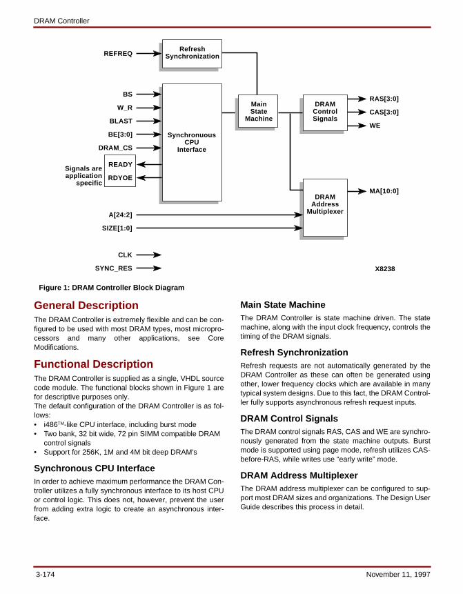
DRAM Controller
General DescriptionThe DRAM Controller is extremely flexible and can be con-figured to be used with most DRAM types, most micropro-cessors and many other applications, see CoreModifications.
Functional DescriptionThe DRAM Controller is supplied as a single, VHDL sourcecode module. The functional blocks shown in Figure 1 arefor descriptive purposes only.The default configuration of the DRAM Controller is as fol-lows:• i486TM-like CPU interface, including burst mode• Two bank, 32 bit wide, 72 pin SIMM compatible DRAM
control signals• Support for 256K, 1M and 4M bit deep DRAM's
Synchronous CPU InterfaceIn order to achieve maximum performance the DRAM Con-troller utilizes a fully synchronous interface to its host CPUor control logic. This does not, however, prevent the userfrom adding extra logic to create an asynchronous inter-face.
Main State MachineThe DRAM Controller is state machine driven. The statemachine, along with the input clock frequency, controls thetiming of the DRAM signals.
Refresh SynchronizationRefresh requests are not automatically generated by theDRAM Controller as these can often be generated usingother, lower frequency clocks which are available in manytypical system designs. Due to this fact, the DRAM Control-ler fully supports asynchronous refresh request inputs.
DRAM Control SignalsThe DRAM control signals RAS, CAS and WE are synchro-nously generated from the state machine outputs. Burstmode is supported using page mode, refresh utilizes CAS-before-RAS, while writes use “early write” mode.
DRAM Address MultiplexerThe DRAM address multiplexer can be configured to sup-port most DRAM sizes and organizations. The Design UserGuide describes this process in detail.
Figure 1: DRAM Controller Block Diagram
X8238
RefreshSynchronization
DRAMControlSignals
DRAMAddress
Multiplexer
REFREQ
RAS[3:0]
CAS[3:0]
WE
BS
SynchronuousCPU
Interface
W_R
BLAST
MA[10:0]
BE[3:0]
DRAM_CS
READY
RDYOESignals areapplication
specific
A[24:2]
SIZE[1:0]
CLK
SYNC_RES
MainState
Machine
3-174 November 11, 1997

NMI Electronics Ltd.
Table 1: Core Signal Pinout
Note: 1. These signals must be applied synchronously to CLOCK.
Core ModificationsAs supplied, the DRAM Controller is designed for optimumperformance in the 40MHz to 50MHz range, using 70nsfast-page-mode DRAM’s. The system interface is i486TM-like.Many system designs will require that the core be modifiedbefore it can be used, especially with regard to the systeminterface. For this reason the core is supplied in sourcecode format, and has been written with modification inmind.The Design User Guide supplied with the core describes indetail how the core can be modified for different system in-terfaces, different clock speeds and different DRAM types
SignalSignal
DirectionDescription
CLOCKInput
Primary system clock; rising edge triggered.
SYNC_RES1
InputSystem reset, synchronous to CLOCK; active High.
BS
Input
Bus cycle start signal; active High. One CLOCK period wide. Identical to inverse of i486TM ADS signal.
W_R1
Input
System read or write cycle indicator. Cannot change state during whole bus cycle, or during a complete burst sequence; 0=read1=write.
BLAST1
Input
Burst last indicator. Active High for last bus cycle in a burst sequence.
BE[3:0]1
Input
Byte enable signals for de-fault, 32 bit configuration. Writes are gated by state of byte enables; however all reads return 32 bit data; ac-tive Low.
DRAM_CS1
Input
Select signal for DRAM Con-troller; active High. Must be active while BS is active for DRAM Controller to respond to a bus cycle. Usually driven by an address decode.
A[24:2]1
Input
System address lines for de-fault, 32 bit configuration; ac-tive High.
SIZE[1:0]
Input
DRAM module size selection inputs. These should not be changed during normal sys-tem operation. For default configuration these are:00 - 256 KBit DRAM’s01 - 1 MBit DRAM’s1x - 4 MBit DRAM’s
REFREQ
Input
Refresh request input; active High. May be asynchronous to CLOCK, and is rising edge triggered. Typical period is 15.625 microseconds maxi-mum.
RAS[3:0]
Output
DRAM RAS outputs; active Low. To be compatible with standard 72 pin SIMM’s, RAS0 and RAS1 are func-tionally identical and drive half of the first bank of DRAM’s each. RAS2 and RAS3 drive half of the sec-ond bank of DRAM’s each.
CAS[3:0]
Output
DRAM CAS outputs; active Low; Configured for fast page mode operation by de-fault and used in early-write mode, when CAS activation is gated by their respective BE’s.
WE
Output
DRAM WE output; active Low. DRAM Controller uses early-write mode, so WE is used as an indicator only.
MA[10:0]
Output
Multiplexed row and column address outputs; active High. Multiplexing scheme deter-mined by state of SIZE in-puts.
READY
Output
System Ready output; active High. Default configuration is for i486TM microprocessor. Output is usually system host specific.
RDYOE
Output
System Ready 3-state en-able output; active High. De-fault configuration utilizes a 3-state driver for System Ready. Output is usually sys-tem host specific.
SignalSignal
DirectionDescription
November 11, 1997 3-175
DRAM Controller
and speeds.Please note that NMI support does not cover user coremodifications. NMI offers design services, including coremodifications, for additional cost.
PinoutThe pin functions of the DRAM Controller core in its defaultconfiguration are shown in Table 1. The pinout is not fixedto any specific CPLD I/O, and can generally be modified tosuit the user’s application.Signal names are provided in the block diagram shown inFigure 1, and described in Table 1.
Verification MethodsBoth functional and timing simulation have been carried outusing ViewSim under Viewlogic Workview OfficeTM. Simula-tion vectors used for verification are provided with the corein the form of ViewSim command files.The core has been extensively tested on target hardwareusing an NMI developed evaluation card.
Recommended Design ExperienceUsers should be familiar with VHDL and Xilinx design flows.Experience with microprocessor or similar system design isrecommended. The core can easily be integrated into hier-archical VHDL designs.
Available Support ProductsNMI has developed a Xilinx core evaluation card and thiswill be available, at additional cost, in the near future.
Ordering InformationTo make further enquiries or purchase the DRAM Control-ler Core, please contact NMI directly at the location detailedon the front page. NMI also offers core integration and de-sign services, the latter covering not only CPLD and FPGAdesign but also complete systems design.NMI cores are purchased under a Licence Agreement, cop-ies of which are available on request.
Related Information
Xilinx Programmable LogicFor information on Xilinx programmable logic or develop-ment system software, contact your local Xilinx sales office,or:
Xilinx, Inc.2100 Logic DriveSan Jose, CA 95124Phone: +1 408-559-7778Fax: +1 408-559-7114URL: www.xilinx.com
For general Xilinx literature, contact:Phone: +1 800-231-3386 (inside the US)
+1 408-879-5017 (outside the US)E-mail: [email protected]
For AllianceCORETM specific information, contact:Phone: +1 408-879-5381E-mail: [email protected]: www.xilinx.com/products/logicore/alliance/
tblpart.htm
3-176 November 11, 1997
General Core Development Tools Table of Contents
February 8, 1998
GVA-100 DSP Prototyping Platform . . . . . . . . . . . . . . . . . . . . . . . . . . . . . . . . . .3-179MDS FPGA Development Module . . . . . . . . . . . . . . . . . . . . . . . . . . . . . . . . . . . .3-183Microprocessor Based Core Evaluation Card . . . . . . . . . . . . . . . . . . . . . . . . . . .3-185
February 8, 1998 3-1773-2

General Core Development Tools Table of Contents
3-178 February 8, 1998
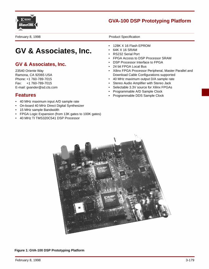
GVA-100 DSP Prototyping Platform
February 8, 1998 Product Specification
GV & Associates, Inc.23540 Oriente WayRamona, CA 92065 USAPhone: +1 760-789-7015Fax: +1 760-789-7015E-mail: [email protected]
Features• 40 MHz maximum input A/D sample rate• On-board 40 MHz Direct Digital Synthesizer• 15 MHz sample Bandwidth• FPGA Logic Expansion (from 13K gates to 100K gates)• 40 MHz TI TMS320C541 DSP Processor
• 128K X 16 Flash EPROM• 64K X 16 SRAM• RS232 Serial Port• FPGA Access to DSP Processor SRAM• DSP Processor Interface to FPGA• 24 bit FPGA Local Bus• Xilinx FPGA Processor Peripheral, Master Parallel and
Download Cable Configurations supported • 40 MHz maximum output D/A sample rate• Stereo Audio Amplifier with Stereo Jack• Selectable 3.3V source for Xilinx FPGAs• Programmable A/D Sample Clock• Programmable DDS Sample Clock
GV & Associates, Inc.
Figure 1: GVA-100 DSP Prototyping Platform
February 8, 1998 3-179
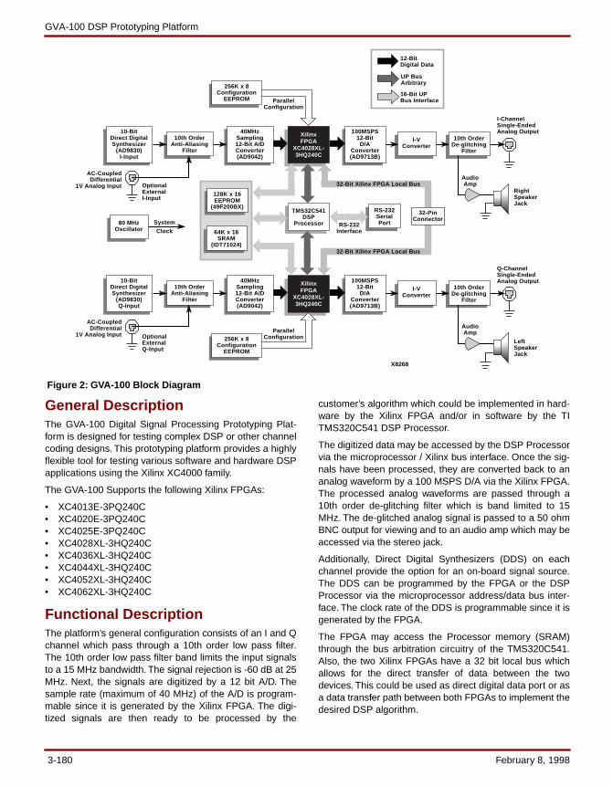
GVA-100 DSP Prototyping Platform
General DescriptionThe GVA-100 Digital Signal Processing Prototyping Plat-form is designed for testing complex DSP or other channelcoding designs. This prototyping platform provides a highlyflexible tool for testing various software and hardware DSPapplications using the Xilinx XC4000 family.
The GVA-100 Supports the following Xilinx FPGAs:
• XC4013E-3PQ240C• XC4020E-3PQ240C• XC4025E-3PQ240C• XC4028XL-3HQ240C• XC4036XL-3HQ240C• XC4044XL-3HQ240C• XC4052XL-3HQ240C• XC4062XL-3HQ240C
Functional DescriptionThe platform’s general configuration consists of an I and Qchannel which pass through a 10th order low pass filter.The 10th order low pass filter band limits the input signalsto a 15 MHz bandwidth. The signal rejection is -60 dB at 25MHz. Next, the signals are digitized by a 12 bit A/D. Thesample rate (maximum of 40 MHz) of the A/D is program-mable since it is generated by the Xilinx FPGA. The digi-tized signals are then ready to be processed by the
customer’s algorithm which could be implemented in hard-ware by the Xilinx FPGA and/or in software by the TITMS320C541 DSP Processor.
The digitized data may be accessed by the DSP Processorvia the microprocessor / Xilinx bus interface. Once the sig-nals have been processed, they are converted back to ananalog waveform by a 100 MSPS D/A via the Xilinx FPGA.The processed analog waveforms are passed through a10th order de-glitching filter which is band limited to 15MHz. The de-glitched analog signal is passed to a 50 ohmBNC output for viewing and to an audio amp which may beaccessed via the stereo jack.
Additionally, Direct Digital Synthesizers (DDS) on eachchannel provide the option for an on-board signal source.The DDS can be programmed by the FPGA or the DSPProcessor via the microprocessor address/data bus inter-face. The clock rate of the DDS is programmable since it isgenerated by the FPGA.
The FPGA may access the Processor memory (SRAM)through the bus arbitration circuitry of the TMS320C541.Also, the two Xilinx FPGAs have a 32 bit local bus whichallows for the direct transfer of data between the twodevices. This could be used as direct digital data port or asa data transfer path between both FPGAs to implement thedesired DSP algorithm.
Figure 2: GVA-100 Block Diagram
I-VConverter
10th OrderDe-glitching
Filter
80 MHzOscillator
XilinxFPGA
XC4028XL-3HQ240C
TMS32C541DSP
Processor
X8268
256K x 8Configuration
EEPROM ParallelConfiguration
RS-232Interface
System
Clock
ParallelConfiguration
RightSpeakerJack
AudioAmp
AudioAmp
I-ChannelSingle-EndedAnalog Output
Q-ChannelSingle-EndedAnalog Output
LeftSpeakerJack
12-BitDigital Data
UP BusArbitrary
40MHzSampling12-Bit A/DConverter(AD9042)
100MSPS12-Bit
D/AConverter(AD9713B)
10-BitDirect DigitalSynthesizer
(AD9830)I-Input
AC-CoupledDifferential
1V Analog Input OptionalExternalI-Input
OptionalExternalQ-Input
AC-CoupledDifferential
1V Analog Input
16-Bit UPBus Interface
10th OrderAnti-Aliasing
Filter
128K x 16EEPROM
(49F200BX)
64K x 16SRAM
(IDT71024)
RS-232SerialPort
I-VConverter
10th OrderDe-glitching
Filter
XilinxFPGA
XC4028XL-3HQ240C
40MHzSampling12-Bit A/DConverter(AD9042)
100MSPS12-Bit
D/AConverter(AD9713B)
10-BitDirect DigitalSynthesizer
(AD9830)Q-Input
10th OrderAnti-Aliasing
Filter
256K x 8Configuration
EEPROM
32-Bit Xilinx FPGA Local Bus
32-Bit Xilinx FPGA Local Bus
32-PinConnector
3-180 February 8, 1998
GVA & Associates, Inc.
Ordering InformationThis product is available directly from GV & Associates.Please contact them for pricing and more information.
Related InformationFor information on Xilinx programmable logic or develop-ment system software, contact your local Xilinx sales office,or:
Xilinx, Inc.2100 Logic DriveSan Jose, CA 95124Phone: +1 408-559-7778Fax: +1 408-559-7114
URL: www.xilinx.com
For general Xilinx literature, contact:
Phone: +1 800-231-3386 (inside the US)+1 408-879-5017 (outside the US)
E-mail: [email protected]
For AllianceCORETM specific information, contact:
Phone: +1 408-879-5381E-mail: [email protected]: www.xilinx.com/products/logicore/alliance/
tblpart.htm
February 8, 1998 3-181
GVA-100 DSP Prototyping Platform
3-182 February 8, 1998
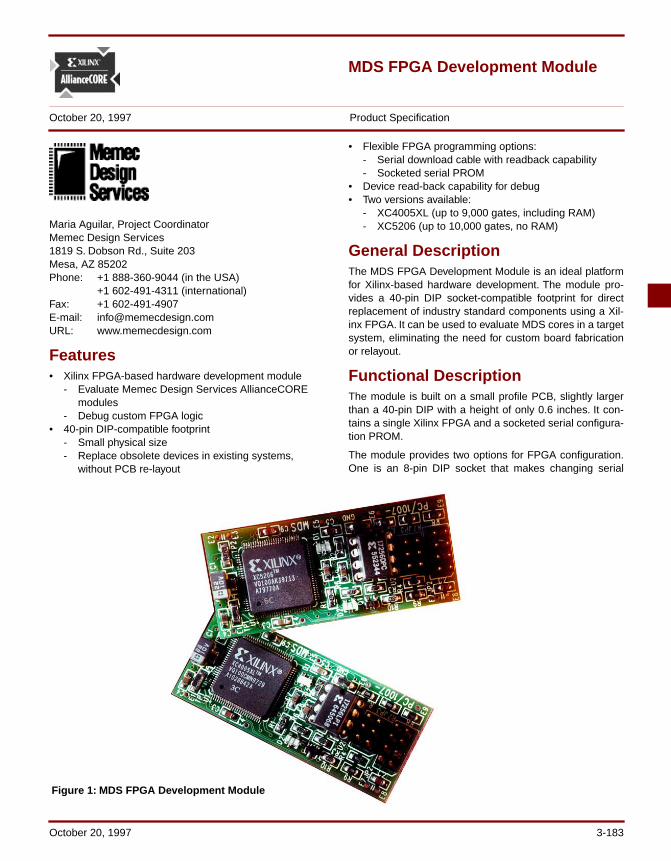
MDS FPGA Development Module
October 20, 1997 Product Specification
Maria Aguilar, Project CoordinatorMemec Design Services1819 S. Dobson Rd., Suite 203Mesa, AZ 85202Phone: +1 888-360-9044 (in the USA)
+1 602-491-4311 (international)Fax: +1 602-491-4907E-mail: [email protected]: www.memecdesign.com
Features• Xilinx FPGA-based hardware development module
- Evaluate Memec Design Services AllianceCORE modules
- Debug custom FPGA logic• 40-pin DIP-compatible footprint
- Small physical size- Replace obsolete devices in existing systems,
without PCB re-layout
• Flexible FPGA programming options:- Serial download cable with readback capability- Socketed serial PROM
• Device read-back capability for debug• Two versions available:
- XC4005XL (up to 9,000 gates, including RAM)- XC5206 (up to 10,000 gates, no RAM)
General DescriptionThe MDS FPGA Development Module is an ideal platformfor Xilinx-based hardware development. The module pro-vides a 40-pin DIP socket-compatible footprint for directreplacement of industry standard components using a Xil-inx FPGA. It can be used to evaluate MDS cores in a targetsystem, eliminating the need for custom board fabricationor relayout.
Functional DescriptionThe module is built on a small profile PCB, slightly largerthan a 40-pin DIP with a height of only 0.6 inches. It con-tains a single Xilinx FPGA and a socketed serial configura-tion PROM.
The module provides two options for FPGA configuration.One is an 8-pin DIP socket that makes changing serial
Figure 1: MDS FPGA Development Module
October 20, 1997 3-183

MDS FPGA Development Module
PROMs easy. This is also an option if the module is to beused in a permanent configuration, such as direct socketreplacement of an existing device.
Alternatively, a serial download cable can be attached toon-board headers and used to configure the FPGA duringthe prototyping stage of the design. It can also be used toperform device readback during debug.
Two versions of the module are available. The first includesa Xilinx XC5206 FPGA that provides up to 10,000 logicgates for 5V systems.
The second includes a Xilinx XC4005XL 3.3V FPGA thatprovides up to 9000 gates, including on-chip RAM. Thismodule can also be used in a 5V system that provides aregulator for the module power supply.
Module power and ground pins match industry-standardconfiguration where ground is at Pin 20 and VCC is Pin 40.
Additional Support ProductsMemec Design Services provides Xilinx FPGA design ser-vices and Xilinx FPGA cores.
MDS has available cores that, when implemented in aDevelopment Module can form direct plug compatiblereplacements for the following industry functions:
• 8250 UART• 8255 Programmable Peripheral Interface• 8256 Peripheral and Multifunction UART• 8279 Keyboard/Display Controller
Ordering InformationThe MDS FPGA Development Module is provided underlicense from Memec Design Services for use in Xilinx pro-grammable logic devices and Xilinx HardWireTM gatearrays. To purchase or make further inquiries about this orother Memec Design Services products, contact MDSdirectly at the location listed on the front page.
Information furnished by Memec Design Services isbelieved to be accurate and reliable. Memec Design Ser-vices reserves the right to change specifications detailed inthis data sheet at any time without notice, in order toimprove reliability, function or design, and assumes noresponsibility for any errors within this document. MemecDesign Services does not make any commitment to updatethis information.
Memec Design Services assumes no obligation to correctany errors contained herein or to advise any user of thistext of any correction, if such be made, nor does the Com-pany assume responsibility for the functioning of unde-scribed features or parameters. Memec Design Serviceswill not assume any liability for the accuracy or correctnessof any support or assistance provided to a user.
Memec Design Services does not represent that productsdescribed herein are free from patent infringement or fromany other third-party right. No license is granted by implica-tion or otherwise under any patent or patent rights ofMemec Design Services.
Memec Design Services products are not intended for usein life support appliances, devices, or systems. Use of aMemec Design Services product in such application with-out the written consent of the appropriate Memec DesignServices officer is prohibited.
All trademarks, registered trademarks, or servicemarks are property of their respective owners.
Related Information
Xilinx Programmable LogicFor information on Xilinx programmable logic or develop-ment system software, contact your local Xilinx sales office,or:
Xilinx, Inc.2100 Logic DriveSan Jose, CA 95124Phone: +1 408-559-7778Fax: +1 408-559-7114URL: www.xilinx.com
For general Xilinx literature, contact:
Phone: +1 800-231-3386 (inside the US)+1 408-879-5017 (outside the US)
E-mail: [email protected]
For AllianceCORETM specific information, contact:
Phone: +1 408-879-5381E-mail: [email protected]: www.xilinx.com/products/logicore/alliance/
tblpart.htm
3-184 October 20, 1997

Microprocessor Based Core Evaluation Card
February 8, 1998 Product Specification
NMI Electronics Ltd.Fountain HouseGreat CornbowHalesowenWest MidlandsB63 3BLUnited KingdomPhone: +44 (0) 121 585 5979Fax: +44 (0) 121 585 5764E-mail: [email protected]: www.nmi.co.uk
Features• Microprocessor based IP Core evaluation card• i486DXTM based system, supporting both +5V and
+3.3V CPU’s with selectable clock speeds up to 50MHz• Single XC95216 system control CPLD with integrated
NMI DRAM Controller Core• XC4000XL site available as a dedicated memory
controller (in place of the XC95216)• Single, industry standard 72 pin SIMM DRAM memory
connector- Configurable for SDRAM operation with custom NMI
module• Parallel connected XC95216 and XC4000E available
for general purpose I/O core integration:- Connected to full 32 bit i486DXTM bus- RS232 port connection- PC-compatible parallel port connection- I2C master/slave controller connection- General purpose pin strip header connection
• XC9500 parts programmable in-circuit via JTAG chain
Figure 1: Microprocessor Based Core Evaluation Card
February 8, 1998 3-185
Microprocessor Based Core Evaluation Card
• XC4000 parts programmable in-circuit via either programming cable or directly from the system CPU
• System support devices include boot EPROM and/or Flash EPROM, SRAM and serial port
• Full featured debug monitor facilitates thorough evaluation and test of cores
• Operates from single +8V to +20V DC input
General DescriptionNMI’s AllianceCORETM Evaluation Card is intended to allowdevelopers to quickly evaluate the functionality of CPU pe-ripheral and memory controller cores. Developers can alsotest, using real target hardware, modifications to the coresand/or their own peripheral logic. This increases confidencethat user designs will be fully functional when integratedinto the final target hardware platform.
Functional DescriptionThe Evaluation Card’s host CPU is i486DXTM and both +5V(e.g. i486DXTM and i486DX2TM) and +3.3V (e.g. i486DX4TM)versions of the CPU are supported. CPU operating voltageis auto-sensed using the standard Intel 486DX4TM mecha-nism.
The i486DXTM has a general purpose, high speed synchro-nous bus and this allows developers to easily migrate de-signs to other microprocessor or system interfaces. Thebus clock speed can be set to a number of frequenciesranging from 16MHz to 66MHz (although the Intel486DX4TM is limited to 50MHz maximum). The bus clock isdistributed using individual, low skew (PLL controlled) clockdrivers to the CPU and each of the Xilinx PLD’s.
The XC95216 system controller CPLD is the only requiredPLD device as it provides all of the basic CPU state and ad-dress decoding. NMI’s AllianceCORE DRAM Controller canalso be integrated into this device, providing the board withincreased memory resources. The CPU has a central re-source of boot EPROM, Flash EPROM, SRAM and RS232serial port with which it can run its built in debug and testmonitor.
An optional XC4KXL device can be used to provide thememory controller function instead of the XC95216 (theXC95216 is still required in the system though). A single, in-dustry standard 72 pin DRAM SIMM connector is providedon the board, allowing the use of any standard SIMM mod-ule with either one or two banks of DRAM. The SIMM powersupply can be set to either +3.3V or +5V. A single configu-ration jumper also allows the bus clock to be routed to a noconnect pin on the SIMM connector, allowing custom Syn-chronous DRAM SIMM modules to be used also.
Two (optional) peripheral controller PLD’s are also providedon the board: an XC95216-HQ208 and an XC4KE-HQ240.The devices are effectively connected in parallel, with one
side each connected to the full i486DXTM system bus, theother side connected to some general purpose I/O. Bothdevices employ +5V I/O buffers.
The general purpose I/O consists of:• A full 9 pin RS232 serial port (level translators provided)• A PC parallel port (ESD protection provided)
• A separate, Philips Semiconductors I2C master/slave controller
• Pin headers (16 off)• Two LED’s
The board is provided with a full featured debug monitorwhich has been optimized for debugging and testing hard-ware. The monitor includes:• Standard memory and I/O display and modification
commands.• Assembly language coded fill and test commands
which ensure maximum CPU bandwidth utilization of memory. These commands are very useful for stress testing designs.
• Software assembler and disassembler (80186 instruction set).
• File transfer via the serial port. Includes binary format plus Intel HEX and Microsoft EXE program loaders.
• Basic DOS INT 21 emulator to ease user test software development.
• Built in macro language.
The two XC95216 devices are configured in a single JTAGchain and can easily be programmed using the XACTstepM1 JTAG CPLD Programmer software. The two XC4K de-vices can be programmed using asynchronous peripheralmode via the debug monitor; alternatively each device isprovided with a separate serial download cable connection.
The Evaluation Card is powered from a single, +8V to +20VDC input. Switched-mode power converters are used, re-sulting in low heat dissipation by the board (other than bythe CPU). The power supplies are protected against inputvoltage reversal.
The Evaluation Card will be CE approved by NMI.
Available Support ProductsNMI will develop a Synchronous DRAM SIMM modulewhich will be compatible with the Evaluation Card and thiswill be available, at additional cost, in the near future.
Ordering InformationTo make further enquiries or purchase the Core EvaluationCard, please contact NMI directly at the location detailed onthe front page. NMI also offers core products and designservices, the latter covering not only CPLD and FPGA de-sign but also complete systems design.
3-186 February 8, 1998
NMI Electronics Ltd.
Related Information
Xilinx Programmable LogicFor information on Xilinx programmable logic or develop-ment system software, contact your local Xilinx sales office,or:
Xilinx, Inc.2100 Logic DriveSan Jose, CA 95124Phone: +1 408-559-7778Fax: +1 408-559-7114URL: www.xilinx.com
For general Xilinx literature, contact:Phone: +1 800-231-3386 (inside the US)
+1 408-879-5017 (outside the US)E-mail: [email protected]
For AllianceCORETM specific information, contact:Phone: +1 408-879-5381E-mail: [email protected]: www.xilinx.com/products/logicore/alliance/
tblpart.htm
February 8, 1998 3-187

Microprocessor Based Core Evaluation Card
3-188 February 8, 1998
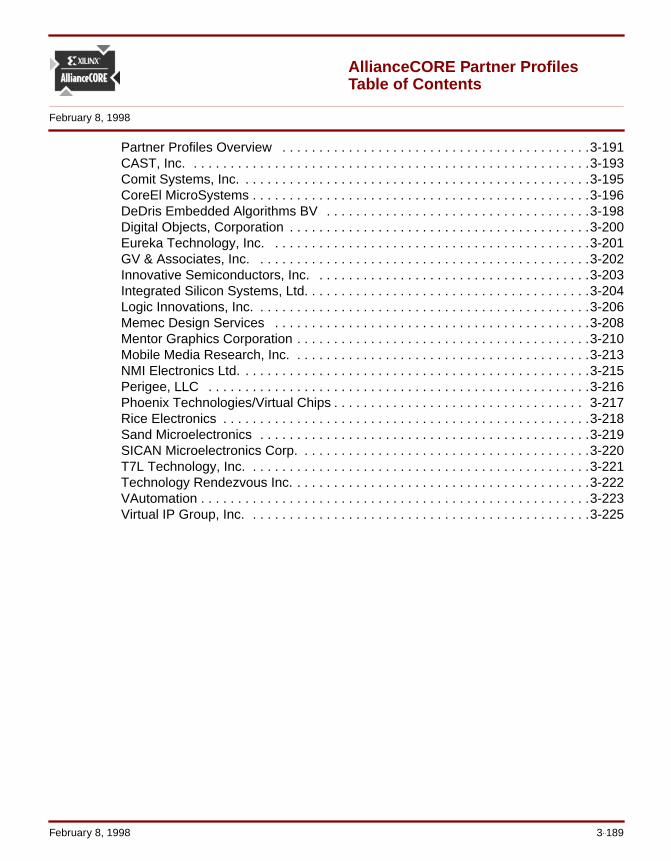
AllianceCORE Partner Profiles Table of Contents
February 8, 1998
Partner Profiles Overview . . . . . . . . . . . . . . . . . . . . . . . . . . . . . . . . . . . . . . . . . .3-191CAST, Inc. . . . . . . . . . . . . . . . . . . . . . . . . . . . . . . . . . . . . . . . . . . . . . . . . . . . . . .3-193Comit Systems, Inc. . . . . . . . . . . . . . . . . . . . . . . . . . . . . . . . . . . . . . . . . . . . . . . .3-195CoreEl MicroSystems . . . . . . . . . . . . . . . . . . . . . . . . . . . . . . . . . . . . . . . . . . . . . .3-196DeDris Embedded Algorithms BV . . . . . . . . . . . . . . . . . . . . . . . . . . . . . . . . . . . .3-198Digital Objects, Corporation . . . . . . . . . . . . . . . . . . . . . . . . . . . . . . . . . . . . . . . . .3-200Eureka Technology, Inc. . . . . . . . . . . . . . . . . . . . . . . . . . . . . . . . . . . . . . . . . . . .3-201GV & Associates, Inc. . . . . . . . . . . . . . . . . . . . . . . . . . . . . . . . . . . . . . . . . . . . . .3-202Innovative Semiconductors, Inc. . . . . . . . . . . . . . . . . . . . . . . . . . . . . . . . . . . . . .3-203Integrated Silicon Systems, Ltd. . . . . . . . . . . . . . . . . . . . . . . . . . . . . . . . . . . . . . .3-204Logic Innovations, Inc. . . . . . . . . . . . . . . . . . . . . . . . . . . . . . . . . . . . . . . . . . . . . .3-206Memec Design Services . . . . . . . . . . . . . . . . . . . . . . . . . . . . . . . . . . . . . . . . . . .3-208Mentor Graphics Corporation . . . . . . . . . . . . . . . . . . . . . . . . . . . . . . . . . . . . . . . .3-210Mobile Media Research, Inc. . . . . . . . . . . . . . . . . . . . . . . . . . . . . . . . . . . . . . . . .3-213NMI Electronics Ltd. . . . . . . . . . . . . . . . . . . . . . . . . . . . . . . . . . . . . . . . . . . . . . . .3-215Perigee, LLC . . . . . . . . . . . . . . . . . . . . . . . . . . . . . . . . . . . . . . . . . . . . . . . . . . . .3-216Phoenix Technologies/Virtual Chips . . . . . . . . . . . . . . . . . . . . . . . . . . . . . . . . . . 3-217Rice Electronics . . . . . . . . . . . . . . . . . . . . . . . . . . . . . . . . . . . . . . . . . . . . . . . . . .3-218Sand Microelectronics . . . . . . . . . . . . . . . . . . . . . . . . . . . . . . . . . . . . . . . . . . . . .3-219SICAN Microelectronics Corp. . . . . . . . . . . . . . . . . . . . . . . . . . . . . . . . . . . . . . . .3-220T7L Technology, Inc. . . . . . . . . . . . . . . . . . . . . . . . . . . . . . . . . . . . . . . . . . . . . . .3-221Technology Rendezvous Inc. . . . . . . . . . . . . . . . . . . . . . . . . . . . . . . . . . . . . . . . .3-222VAutomation . . . . . . . . . . . . . . . . . . . . . . . . . . . . . . . . . . . . . . . . . . . . . . . . . . . . .3-223Virtual IP Group, Inc. . . . . . . . . . . . . . . . . . . . . . . . . . . . . . . . . . . . . . . . . . . . . . .3-225
February 8, 1998 3-189

AllianceCORE Partner Profiles Table of Contents
3-190 February 8, 1998
February 8, 1998
Partner Profiles Overview
OverviewXilinx is proud to present our AllianceCORE partner com-panies. Each is an expert in its respective field and ready toassist you with products and services for your application.This section profiles each partner and their particular areasof expertise. This way, you can learn more about the part-ners since many of them may be new to you.
Most partners supply products and services unrelated tothe AllianceCORE program that may be of value to you.These are profiled in tables under the Areas of TechnicalExpertise section for each partner. It is from this pool of
products and knowledge that future AllianceCORE prod-ucts will emerge.
Some partners have Xilinx versions of cores that have yetto go through the process to become AllianceCORE’s.Other cores may never make this transition because a pro-grammable logic implementation is not practical today. Alli-anceCORE products are clearly differentiated in separateAllianceCORE Product Tables. Each also has a completedatasheet in the AllianceCORE Products section of thisdatabook.
February 8, 1998 3-191

AllianceCORE Partner Profiles
3-192 February 8, 1998
Partner Profile
February 8, 1998
CAST, Inc.
24 White Birch DrivePomona, NY 10970 USAPhone: +1 914 354-4945Fax: +1 914 354-0325E-mail: [email protected]: www.cast-inc.com
OverviewCAST focuses on maximizing the success of FPGAdesigns by supplying high-quality, high-value models forsimulation and synthesis. CAST provides a total modelingsolution for FPGA design by delivering and supportingaccurate, reliable, and affordable VHDL models ready foruse by designers worldwide. CAST supplies a variety ofsupport programs, VHDL training programs, consulting ser-vices, and custom modeling services.
CAST's products includes:
• V-Custom Cores - optimized synthesizable cores developed in VHDL for FPGA and ASIC designs. Available cores include UARTs, DMA controllers, interrupt controllers, bus interfaces, microcontrollers, and processors.
• Standard Component VHDL Library - Synthesizable (SCVL-S) consisting of over 600 VHDL synthesizable models of generic and TTL functions. Developed for new FPGA designs, and for conversion of older TTL circuits into FPGAs.
• Pre-packaged libraries feature Standard Component VHDL Library (SCVL) series. Developed for system and device designers, SCVL includes simulation models for 3,000 memory devices and 2,500 standard ECL and TTL devices.
• V-Custom Models - VHDL simulation models for processors, complex functions, and specialized devices. Featuring in-stock models such as the Pentium processor and a variety of peripherals
AllianceCORE ProductsTable 1 shows released AllianceCORE products availablefrom CAST. Datasheets of these products are included inthe AllianceCORE Products section of this databook. Con-tact CAST for pricing.
Additional Areas of ExpertiseTable 2 shows CAST, Inc.’s areas of technical expertise. Xil-inx and CAST are in the process of evaluating these todetermine which are suitable as AllianceCORE products. Ifyou have a need for a specific product then contact CAST,Inc. for information or availability.
Function Description DatasheetBase Level FunctionsC2910A Microprogram Controller 3-129Communication and NetworkingViterbi Decoder Viterbi Decoder 3-91
Table 1: Released AllianceCORE Products
February 8, 1998 3-193

AllianceCORE Partner Profiles
.
Function Description GatesBase Level FunctionsC_UART Generic UART 650C49410 Microprogram Controller 9,500C29116A 16-Bit MicroprocessorC6850 Asynchronous Communications Interface 1,300C8051 MicrocontrollerC8251 USARTC8254 Programmable Timer/CounterC8255 Parallel Interface PeripheralC8259 Programmable Interrupt Controller
Table 2: CAST Expertise
3-194 February 8, 1998
Partner Profile
February 8, 1998
Comit Systems, Inc.
1250 Oakmead Parkway, Suite 210Sunnyvale, CA 94088 USAPhone: +1 408 988 7966Fax: +1 408 988 2133E-mail: [email protected]: www.comit.com
OverviewComit System, Inc. is a systems engineering companyoffering expertise in the areas of FPGA and ASIC designand development.
Comit Systems hardware design services include:
• FPGA/ASIC designs• PCI design and Xilinx PCI macro customization• HDL (VHDL/Verilog) based designs• Design verification (PLI, simulation, test vector
generation)
To enhance the productivity of its customers, Comit offers aset of efficient libraries for HDL-based Xilinx designs.These modules are available as VHDL/Verilog netlists. InHDL design, they can be instantiated to get maximum effi-ciency. Using constraint files, optimum placement can alsobe achieved. Simulation models provided for functionalsimulation. Higher level macro-modules are also underdevelopment. The areas of development include bus mod-els, communication and DSP cores.
Areas of Technical ExpertiseTable 1 shows Comit Systems areas of technical expertise.Xilinx and Comit are in the process of evaluating these todetermine which are suitable as AllianceCORE products. Ifyou have a need for a specific product then contact Comitfor information or availability.
Function Description CLB’sBase Level FunctionsUART 16450 compatible 130HDLC controller 200Wallace Tree Mul-tiplier
8 x8 Multiplier120
4B/5B Encoder-decoder
9
PRBS Generator Variable length (4-32) 2-33
Table 1: Comit Systems Expertise
February 8, 1998 3-195
Partner Profile
February 8, 1998
CoreEloMicroSystems
CoreEl MicroSystems
46750 Fremont Blvd. #208Fremont, CA 94538 USAPhone: +1 510 770-2277Fax: +1 510 770-2288E-mail: [email protected]: www.coreel.com
OverviewCoreEl MicroSystems offers an extensive list of ATM "CoreCell" designs that have been specifically optimized for usein Xilinx FPGAs. The majority of the IP for the ATM corescomes from the development of a single-chip 155 MbpsNetwork Interface Card (NIC) and a two-chip ATM switchdesign.
AllianceCORE ProductsTable 1 shows released AllianceCORE products availablefrom CoreEl MicroSystems. Datasheets of these productsare included in the AllianceCORE Products section of thisdatabook. Contact CoreEl for pricing.
Additional Areas of Technical Expertise Table 2 shows CoreEl Microsystem’s areas of technicalexpertise. Xilinx and CoreEl are in the process of evaluat-ing these to determine which are suitable as AllianceCOREproducts. If you have a need for a specific product then con-tact CoreEl for information or availability.
Product Functional Description Datasheet Communications and NetworkingCell Assembler Cell stream assembler Corecell 3-49Cell Delineation Cell delineation Corecell 3-53CRC10 CRC10 generator and verifier modules 3-57CRC32 CRC32 generator and verifier modules 3-61UTOPIA Slave UTOPIA Level 2 slave transmitter and receiver modules 3-85
Product Functional Description Gates Communications and NetworkingCS-1000 Gigabit Ethernet MACCS-1001 Gigabit Ethernet 8B/10BCS-1002 Gigabit Ethernet Auto NegationCS-1000T General purpose Gigabit Ethernet user programmable test benchCS-1003 Flow ControlCS-1100 Fast 10/100 Ethernet Media Access ControllerCS-1101 RMII (Reduced Media Independent Interface)TC-25 20 Mbps Transmission ConvergenceTC-622 622 Mbps Transmission ConvergenceTC-34 E3 Transmission ConvergenceTC-45 DS-3 Transmission ConvergenceTC-155 STS-3 Transmission ConvergenceCS-203 ATM Cell diagnostic generation/analysisCC-204 ATM Traffic Policer
Table 2: CoreEl MicroSystems Expertise
Table 1: Released AllianceCORE Products
3-196 February 8, 1998
CoreEl Microsystems
CC-140 UTOPIA MasterSAR-155 ATM Segmentation and ReassemblySAR-622 ATM Segmentation and ReassemblyNIC-155 Single Chip 155 Mbps ATM Network Interface ControllerCC-303 E1 FrameCC-305 E3 FramerCC-307 STS-1 FramerCC-309 STS-3 FramerCC-311 STS-12 FramerCC-315 DS3 PLCP ProcessorCC-316 SONET/SDH Pointer Tracking 15,000CC-316 HDLC controllerCC-317 Multi-channel HDLC controller 2,200
Product Functional Description Gates
February 8, 1998 3-197
Partner Profile
February 8, 1998
DeDris Embedded Algorithms BVMarconistraat 344004 JM TIELTHE NETHERLANDSPhone: +31 344 63 28 38Fax: +31 344 63 26 31Email : [email protected] : www.dedris.nl
OverviewDeDris Embedded Algorithms is specialized in the mappingof complex application-specific signal processing algo-rithms onto dedicated custom hardware architectures.DeDris bridges the gap between algorithm design anddevelopment in high-level languages (such as C, Matlab orPseudo-code) and custom digital processing architectures.Extremely efficient implementations are gained throughcombined optimization on algorithmic, architectural andgate level. Implementations of DeDris’ signal processingalgorithms are named DSP Instant Components and areavailable in Synthesizable VHDL, various netlist formatsand as hard-coded plug and play FPGA and ASIC macroblocks.
The advantages of DeDris’ DSP Instant Components are:
• Direct implementation of complex advanced signal-processing blocks
• Compliance with standards and norms• Significant reduction of time-to-market and design cost• Very efficient implementation• Possibility to create very compact multiple channel
implementations• Customer support on both hardware and algorithm level
In addition to DSP Instant Components, DeDris offers cus-tom design and implementation of application-specific sig-nal processing algorithms. Our mathematicians understandand optimize your processing needs. Together with DeDris’architecture and hardware-design engineers, they createfast and optimized solutions for your application. Turn-around times from algorithm to silicon in weeks and monthsrather than years are feasible when teaming with DeDris.DeDris also has in-depth knowledge of ITU and CCITTstandards. Our application engineers can guide youthrough the possibilities. Together we select the best algo-rithms for your application, which we instantly implement inhardware for you.
DeDris has a strong expertise in speech-related technolo-gies. Multiple speech-compression algorithms have beenimplemented offering toll quality speech compression, andbit rates from 32 kbit/sec down to 2.4 kbit/sec. In addition,DeDris has developed expertise in the fields of speech rec-ognition and synthesis. A further area of expertise is tele-communication. Several popular blocks have beenimplemented by DeDris, which allow rapid development ofcomplex telecommunication systems. DeDris is stronglyextending its fields of expertise through in-house R&D andthe formation of strategic alliances with scientific and indus-trial partners. Areas being developed are audio, video andvision, and radar.
Areas of ExpertiseThe following table of products demonstrates areas ofDeDris technical expertise. Xilinx and Dedris are in the pro-cess of evaluating these to determine which are suitable asAllianceCORE products. If you have a need for a specificproduct then contact Dedris for information or availability.
3-198 February 8, 1998
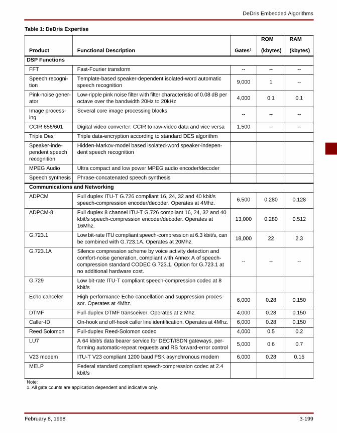
DeDris Embedded Algorithms
Table 1: DeDris Expertise
Product Functional Description Gates 1
ROM
(kbytes)
RAM
(kbytes)
DSP Functions
FFT Fast-Fourier transform -- -- --
Speech recogni-tion
Template-based speaker-dependent isolated-word automatic speech recognition
9,000 1 --
Pink-noise gener-ator
Low-ripple pink noise filter with filter characteristic of 0.08 dB per octave over the bandwidth 20Hz to 20kHz
4,000 0.1 0.1
Image process-ing
Several core image processing blocks-- -- --
CCIR 656/601 Digital video converter: CCIR to raw-video data and vice versa 1,500 -- --
Triple Des Triple data-encryption according to standard DES algorithm
Speaker-inde-pendent speech recognition
Hidden-Markov-model based isolated-word speaker-indepen-dent speech recognition
MPEG Audio Ultra compact and low power MPEG audio encoder/decoder
Speech synthesis Phrase-concatenated speech synthesis
Communications and Networking
ADPCM Full duplex ITU-T G.726 compliant 16, 24, 32 and 40 kbit/s speech-compression encoder/decoder. Operates at 4Mhz.
6,500 0.280 0.128
ADPCM-8 Full duplex 8 channel ITU-T G.726 compliant 16, 24, 32 and 40 kbit/s speech-compression encoder/decoder. Operates at 16Mhz.
13,000 0.280 0.512
G.723.1 Low bit-rate ITU compliant speech-compression at 6.3 kbit/s, can be combined with G.723.1A. Operates at 20Mhz.
18,000 22 2.3
G.723.1A Silence compression scheme by voice activity detection and comfort-noise generation, compliant with Annex A of speech-compression standard CODEC G.723.1. Option for G.723.1 at no additional hardware cost.
-- -- --
G.729 Low bit-rate ITU-T compliant speech-compression codec at 8 kbit/s
Echo canceler High-performance Echo-cancellation and suppression proces-sor. Operates at 4Mhz.
6,000 0.28 0.150
DTMF Full-duplex DTMF transceiver. Operates at 2 Mhz. 4,000 0.28 0.150
Caller-ID On-hook and off-hook caller line identification. Operates at 4Mhz. 6,000 0.28 0.150
Reed Solomon Full-duplex Reed-Solomon codec 4,000 0.5 0.2
LU7 A 64 kbit/s data bearer service for DECT/ISDN gateways, per-forming automatic-repeat requests and RS forward-error control
5,000 0.6 0.7
V23 modem ITU-T V23 compliant 1200 baud FSK asynchronous modem 6,000 0.28 0.15
MELP Federal standard compliant speech-compression codec at 2.4 kbit/s
Note:1. All gate counts are application dependent and indicative only.
February 8, 1998 3-199
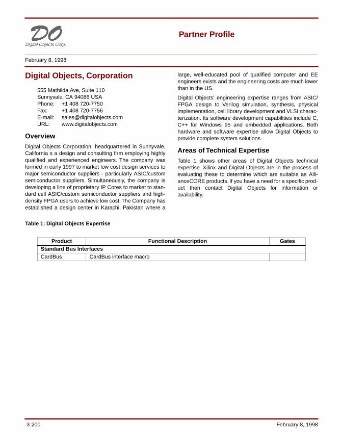
Partner Profile
February 8, 1998
Digital Objects, Corporation
555 Mathilda Ave, Suite 110 Sunnyvale, CA 94086 USA Phone: +1 408 720-7750 Fax: +1 408 720-7756 E-mail: [email protected] URL: www.digitalobjects.com
Overview Digital Objects Corporation, headquartered in Sunnyvale,California s a design and consulting firm employing highlyqualified and experienced engineers. The company wasformed in early 1997 to market low cost design services tomajor semiconductor suppliers - particularly ASIC/customsemiconductor suppliers. Simultaneously, the company isdeveloping a line of proprietary IP Cores to market to stan-dard cell ASIC/custom semiconductor suppliers and high-density FPGA users to achieve low cost. The Company hasestablished a design center in Karachi, Pakistan where a
large, well-educated pool of qualified computer and EEengineers exists and the engineering costs are much lowerthan in the US.
Digital Objects' engineering expertise ranges from ASIC/FPGA design to Verilog simulation, synthesis, physicalimplementation, cell library development and VLSI charac-terization. Its software development capabilities include C,C++ for Windows 95 and embedded applications. Bothhardware and software expertise allow Digital Objects toprovide complete system solutions.
Areas of Technical ExpertiseTable 1 shows other areas of Digital Objects technicalexpertise. Xilinx and Digital Objects are in the process ofevaluating these to determine which are suitable as Alli-anceCORE products. If you have a need for a specific prod-uct then contact Digital Objects for information oravailability.
Product Functional Description GatesStandard Bus Interfaces CardBus CardBus interface macro
Table 1: Digital Objects Expertise
3-200 February 8, 1998
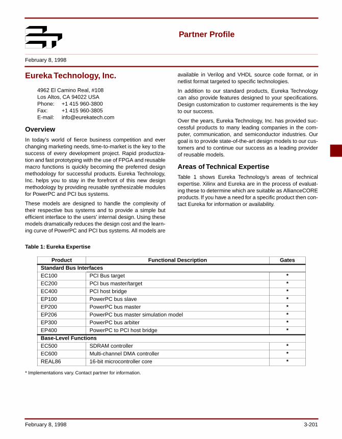
Partner Profile
February 8, 1998
Eureka Technology, Inc.
4962 El Camino Real, #108Los Altos, CA 94022 USAPhone: +1 415 960-3800Fax: +1 415 960-3805 E-mail: [email protected]
OverviewIn today's world of fierce business competition and everchanging marketing needs, time-to-market is the key to thesuccess of every development project. Rapid productiza-tion and fast prototyping with the use of FPGA and reusablemacro functions is quickly becoming the preferred designmethodology for successful products. Eureka Technology,Inc. helps you to stay in the forefront of this new designmethodology by providing reusable synthesizable modulesfor PowerPC and PCI bus systems.
These models are designed to handle the complexity oftheir respective bus systems and to provide a simple butefficient interface to the users' internal design. Using thesemodels dramatically reduces the design cost and the learn-ing curve of PowerPC and PCI bus systems. All models are
available in Verilog and VHDL source code format, or innetlist format targeted to specific technologies.
In addition to our standard products, Eureka Technologycan also provide features designed to your specifications.Design customization to customer requirements is the keyto our success.
Over the years, Eureka Technology, Inc. has provided suc-cessful products to many leading companies in the com-puter, communication, and semiconductor industries. Ourgoal is to provide state-of-the-art design models to our cus-tomers and to continue our success as a leading providerof reusable models.
Areas of Technical Expertise Table 1 shows Eureka Technology’s areas of technicalexpertise. Xilinx and Eureka are in the process of evaluat-ing these to determine which are suitable as AllianceCOREproducts. If you have a need for a specific product then con-tact Eureka for information or availability.
* Implementations vary. Contact partner for information.
Product Functional Description GatesStandard Bus InterfacesEC100 PCI Bus target *EC200 PCI bus master/target *EC400 PCI host bridge *EP100 PowerPC bus slave *EP200 PowerPC bus master *EP206 PowerPC bus master simulation model *EP300 PowerPC bus arbiter *EP400 PowerPC to PCI host bridge *Base-Level FunctionsEC500 SDRAM controller *EC600 Multi-channel DMA controller *REAL86 16-bit microcontroller core *
Table 1: Eureka Expertise
February 8, 1998 3-201
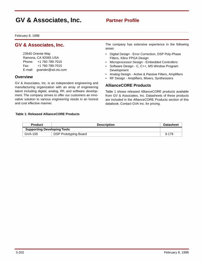
3-202 February 8, 1998
Partner Profile
GV & Associates, Inc.
23540 Oriente Way Ramona, CA 92065 USA Phone: +1 760 789-7015 Fax: +1 760 789-7015 E-mail: [email protected]
OverviewGV & Associates, Inc. is an independent engineering andmanufacturing organization with an array of engineeringtalent including digital, analog, RF, and software develop-ment. The company strives to offer our customers an inno-vative solution to various engineering needs in an honestand cost effective manner.
The company has extensive experience in the followingareas:
• Digital Design - Error Correction, DSP Poly-Phase Filters, Xilinx FPGA Design
• Microprocessor Design - Embedded Controllers• Software Design - C, C++, MS Window Program
Development • Analog Design - Active & Passive Filters, Amplifiers • RF Design - Amplifiers, Mixers, Synthesizers
AllianceCORE ProductsTable 1 shows released AllianceCORE products availablefrom GV & Associates, Inc. Datasheets of these productsare included in the AllianceCORE Products section of thisdatabook. Contact GVA Inc. for pricing.
GV & Associates, Inc.
Table 1: Released AllianceCORE Products
Product Description Datasheet Supporting Developing ToolsGVA-100 DSP Prototyping Board 3-179
February 8, 1998
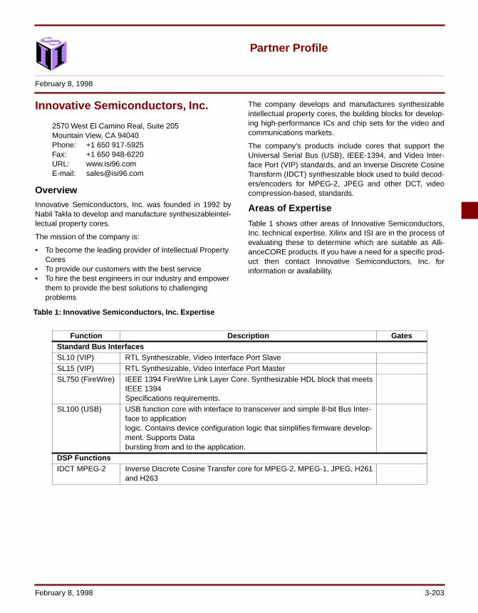
February 8, 1998 3-203
Partner Profile
Innovative Semiconductors, Inc.
2570 West El Camino Real, Suite 205Mountain View, CA 94040Phone: +1 650 917-5925Fax: +1 650 948-6220URL: www.isi96.comE-mail: [email protected]
OverviewInnovative Semiconductors, Inc. was founded in 1992 byNabil Takla to develop and manufacture synthesizableintel-lectual property cores.
The mission of the company is:
• To become the leading provider of Intellectual Property Cores
• To provide our customers with the best service• To hire the best engineers in our industry and empower
them to provide the best solutions to challenging problems
The company develops and manufactures synthesizableintellectual property cores, the building blocks for develop-ing high-performance ICs and chip sets for the video andcommunications markets.
The company's products include cores that support theUniversal Serial Bus (USB), IEEE-1394, and Video Inter-face Port (VIP) standards, and an Inverse Discrete CosineTransform (IDCT) synthesizable block used to build decod-ers/encoders for MPEG-2, JPEG and other DCT, videocompression-based, standards.
Areas of Expertise
Table 1 shows other areas of Innovative Semiconductors,Inc. technical expertise. Xilinx and ISI are in the process ofevaluating these to determine which are suitable as Alli-anceCORE products. If you have a need for a specific prod-uct then contact Innovative Semiconductors, Inc. forinformation or availability.
Function Description GatesStandard Bus InterfacesSL10 (VIP) RTL Synthesizable, Video Interface Port SlaveSL15 (VIP) RTL Synthesizable, Video Interface Port MasterSL750 (FireWire) IEEE 1394 FireWire Link Layer Core. Synthesizable HDL block that meets
IEEE 1394 Specifications requirements.
SL100 (USB) USB function core with interface to transceiver and simple 8-bit Bus Inter-face to application logic. Contains device configuration logic that simplifies firmware develop-ment. Supports Data bursting from and to the application.
DSP FunctionsIDCT MPEG-2 Inverse Discrete Cosine Transfer core for MPEG-2, MPEG-1, JPEG, H261
and H263
February 8, 1998
Table 1: Innovative Semiconductors, Inc. Expertise

Partner Profile
February 8, 1998
Integrated Silicon Systems, Ltd.
50 Malone Rd.Belfast, BT9 5BSNorthern Ireland Phone: +44 1232 664 664 Fax: +44 1232 669 664 E-mail: [email protected] URL: www.iss-dsp.com
OverviewIntegrated Silicon Systems is a DSP intellectual propertycompany specializing in synthesizable DSP products. ISShas an acknowledged worldwide competence in VLSIarchitectures for DSP and supplies highly optimized DSPcircuit functions for ASIC, FPGA and CPLD implementa-tions.
The key advantages of using ISS products are:
• Highly efficient silicon implementations after synthesis• Dramatically reduced design times for rapid prototyping
and fast time-to-market• Very high performance - orders of magnitude greater
than programmable DSP cores• Characterized for the worlds principal fabrication
processes
ISS’s main products are:
• DSP system-level cores - A range of parameterized system level blocks (JPEG, ADPCM) for efficient ASIC, FPGA and CPLD implementation.
• DSP function-level cores - An extensive range of highly parameterized DSP function level blocks for efficient ASIC, FPGA and CPLD implementation.
• DSP ASIC library - A comprehensive library of over 170 parameterized, synthesizable DSP building blocks written in VHDL and are available in a number of fixed and floating point formats.
All blocks are fully parameterized, allowing the ultimate indesign flexibility and design reuse. ISS’s range of functionsis optimized for Xilinx FPGAs, giving Xilinx customers aunique advantage in the design of complex FPGA-basedsystems.
AllianceCORE ProductsTable 1 shows released AllianceCORE products availablefrom ISS. Datasheets for these are included in the Alli-anceCORE Products section of the databook. Contact ISSfor pricing.
Additional Areas of Technical ExpertiseTable 2 shows other areas of ISS’ technical expertise. Xilinxand ISS are in the process of evaluating these to determinewhich are suitable as AllianceCORE products. If you have aneed for a specific product then contact ISS for informationor availability.
Product Functional Description DatasheetDSP FunctionsReed-Solomon High performance R-S encoders 3-77Reed-Solomon High performance R-S decoders 3-71Communications and NetworkingHDLC HDLC Protocol Core 3-65
Table 1: Released AllianceCORE Products
3-204 February 8, 1998
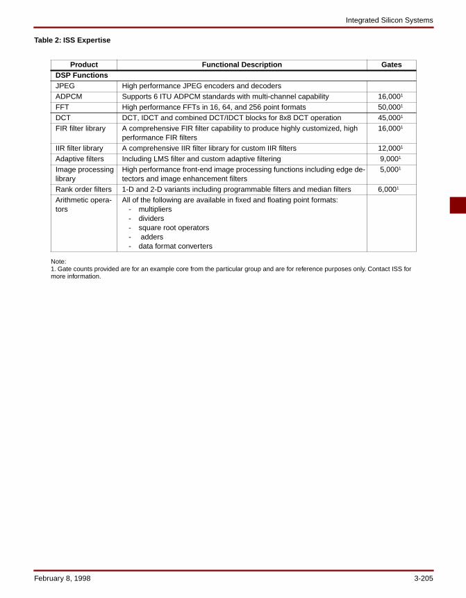
Integrated Silicon Systems
Note: 1. Gate counts provided are for an example core from the particular group and are for reference purposes only. Contact ISS for more information.
Product Functional Description GatesDSP FunctionsJPEG High performance JPEG encoders and decodersADPCM Supports 6 ITU ADPCM standards with multi-channel capability 16,0001
FFT High performance FFTs in 16, 64, and 256 point formats 50,0001
DCT DCT, IDCT and combined DCT/IDCT blocks for 8x8 DCT operation 45,0001
FIR filter library A comprehensive FIR filter capability to produce highly customized, high performance FIR filters
16,0001
IIR filter library A comprehensive IIR filter library for custom IIR filters 12,0001
Adaptive filters Including LMS filter and custom adaptive filtering 9,0001
Image processing library
High performance front-end image processing functions including edge de-tectors and image enhancement filters
5,0001
Rank order filters 1-D and 2-D variants including programmable filters and median filters 6,0001
Arithmetic opera-tors
All of the following are available in fixed and floating point formats:- multipliers- dividers- square root operators- adders- data format converters
Table 2: ISS Expertise
February 8, 1998 3-205
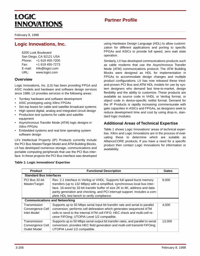
Partner Profile
February 8, 1998
Logic Innovations, Inc.
6205 Lusk Boulevard San Diego, CA 92121 USA Phone: +1 619 455-7200 Fax: +1 619 455-7273 E-mail: [email protected] URL: www.logici.com
OverviewLogic Innovations, Inc. (LII) has been providing FPGA andASIC models and hardware and software design servicessince 1986. LII provides services in the following areas:
• Turnkey hardware and software development• ASIC prototyping using Xilinx FPGAs • Set-top boxes for cable and satellite broadcast systems• High speed digital, analog and integrated circuit design• Production test systems for cable and satellite
equipment• Asynchronous Transfer Mode (ATM) logic designs in
Xilinx FPGAs• Embedded systems and real time operating system
software design
LII’s Intellectual Property (IP) Products currently includethe PCI Bus Master/Target Model and ATM Building Blocks.LII has developed numerous storage, communications andportable computing peripherals that use the PCI Bus inter-face. In these projects the PCI Bus interface was developed
using Hardware Design Language (HDL) to allow customi-zation for different applications and porting to specificFPGAs and ASICs to provide full speed, zero wait stateoperation.
Similarly, LII has developed communications products suchas cable modems that use the Asynchronous TransferMode (ATM) communications protocol. The ATM BuildingBlocks were designed as HDL for implementation inFPGAs to accommodate design changes and multipleproduct configurations. LII has now released these tried-and-proven PCI Bus and ATM HDL models for use by sys-tem designers who demand fast time-to-market, designflexibility and the ability to customize. These products areavailable as source code in VHDL or Verilog format, orobject code in device-specific netlist format. Demand forthe IP Products is rapidly increasing commensurate withgate capacities in ASICs and FPGAs, as designers seek toreduce development time and cost by using drop-in, stan-dard logic modules.
Additional Areas of Technical Expertise Table 1 shows Logic Innovations’ areas of technical exper-tise. Xilinx and Logic Innovations are in the process of eval-uating these to determine which are suitable asAllianceCORE products. If you have a need for a specificproduct then contact Logic Innovations for information oravailability.
Product Functional Description Gates Standard Bus Interfaces PCI Bus 32-bit Master/Target
Rev. 2.1 interface in Verilog or VHDL. Supports full speed burst memory transfers (up to 132 MBps) with a simplified, synchronous local bus inter-face. 16-word by 32-bit transfer buffer of size 2K to 4K; address and data parity generation and checking, and PCI interrupt support. Includes a com-plete HDL test bench to verify compliance.
9,000
Communications and NetworkingTransmission Convergence Cell Inlet Model
Supports up to 50 Mbps serial input bit transfer rate and serial to parallel conversion; performs cell delineation which generates sequenced ATM cells to send to the internal ATM cell FIFO; HEC check and multi-cell re-ceive FIFOing; UTOPIA Level 1/2 compatible.
4,000
Transmission Convergence Cell Outlet Model
Supports up to 50 Mbps serial output bit transfer rates, and parallel to serial conversion; provides HEC field generation and multi-cell transmit FIFOing; UTOPIA Level 1/2 compatible.
13,000
Table 1: Logic Innovations’ Expertise
3-206 February 8, 1998
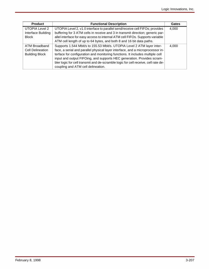
Logic Innovations, Inc.
UTOPIA Level 2 Interface Building Block
UTOPIA Level 2, v1.0 interface to parallel send/receive cell FIFOs; provides buffering for 3 ATM cells in receive and 3 in transmit direction; generic par-allel interface for easy access to internal ATM cell FIFOs. Supports variable ATM cell length of up to 64 bytes, and both 8 and 16 bit data paths.
4,000
ATM Broadband Cell Delineation Building Block
Supports 1.544 Mbit/s to 155.53 Mbit/s. UTOPIA Level 2 ATM layer inter-face, a serial and parallel physical layer interface, and a microprocessor in-terface for configuration and monitoring functions. It includes multiple cell input and output FIFOing, and supports HEC generation. Provides scram-bler logic for cell transmit and de-scramble logic for cell receive, cell rate de-coupling and ATM cell delineation.
4,000
Product Functional Description Gates
February 8, 1998 3-207
Partner Profile
February 8, 1998
Memec Design Services
1819 S. Dobson Rd., Ste. 203Mesa, Arizona 85202 USAPhone: +1 888 360-9044
+1 602 491-4311Fax: +1 602 491-4907 E-mail: [email protected] URL: www.memecdesign.com
OverviewMemec Design Services (MDS) is a subsidiary of theMemec International Components Group -- one of the topten electronics distributors in the world. MDS is part ofRaab Karcher, AG, a $10 billion organization in Essen,Germany. At the top of MDS’ financial stability is Veba, thefourth largest company in Germany.
MDS is dedicated to bringing you the best Xilinx design ser-vices available in the market today. MDS’ design engineershave extensive programmable logic (PLD, CPLD, FPGA,ASIC) design experience (9+ years on average). We areequipped with the tools to complete the design on-time andto your specifications.
New Designs• Project feasibility studies• Xilinx development system selection• Optimal Xilinx FPGA selection• Logic design and capture• Custom macro design• High performance state machine design• Time constraint design• Partioning/mapping control• Floorplanning/placement constraints• Package pin assignment• Timing simulation
Existing Designs• Xilinx design review from FPGA design to system
integration• Xilinx troubleshooting• Conversion of ASIC, FPGA, and CPLD designs to Xilinx• Recapture of Xilinx FPGA designs from LCA or
obsolete CAE tools• Xilinx FPGA performance improvement• Xilinx functional and timing simulation• HardWire conversion
In today’s competitive, fast-paced market environment,engineering managers are under the gun to get designprojects finished on schedule. The lost revenue and marketshare associated with missing a product release date canbe devastating. MDS understands this competitive environ-ment. We can augment your design team’s effort to get yourdesign projects completed on time, improving both time-to-market and time-to-volume for your product. MDS is willingto co-op the development effort and license the design at asubstantially reduced rate.
AllianceCORE ProductsTable 1 shows released AllianceCORE products availablefrom MDS. Datasheets for these are included in the Alli-anceCORE Products section of this databook. ContactMDS for pricing.
Additional Areas of Technical ExpertiseTable 2 shows areas of MDS’ technical expertise. Xilinx andMDS are in the process of evaluating these to determinewhich are suitable as AllianceCORE products. If you have aneed for a specific product then contact MDS for informa-tion or availability.
3-208 February 8, 1998
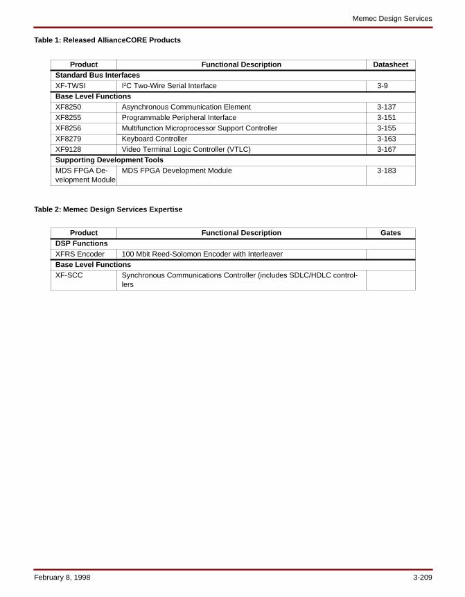
Memec Design Services
Product Functional Description DatasheetStandard Bus InterfacesXF-TWSI I2C Two-Wire Serial Interface 3-9Base Level FunctionsXF8250 Asynchronous Communication Element 3-137XF8255 Programmable Peripheral Interface 3-151XF8256 Multifunction Microprocessor Support Controller 3-155XF8279 Keyboard Controller 3-163XF9128 Video Terminal Logic Controller (VTLC) 3-167Supporting Development ToolsMDS FPGA De-velopment Module
MDS FPGA Development Module 3-183
Product Functional Description GatesDSP FunctionsXFRS Encoder 100 Mbit Reed-Solomon Encoder with InterleaverBase Level FunctionsXF-SCC Synchronous Communications Controller (includes SDLC/HDLC control-
lers
Table 2: Memec Design Services Expertise
Table 1: Released AllianceCORE Products
February 8, 1998 3-209
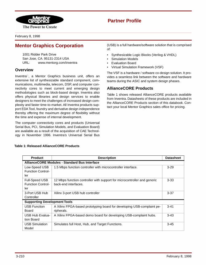
Partner Profile
February 8, 1998
Mentor Graphics Corporation
1001 Ridder Park DriveSan Jose, CA. 95131-2314 USAURL: www.mentorg.com/inventra
OverviewInventra , a Mentor Graphics business unit, offers anextensive list of synthesizable standard component, com-munications, multimedia, telecom, DSP, and computer con-nectivity cores to meet current and emerging designmethodologies such as block-based design. Inventra alsooffers physical libraries and design services to enabledesigners to meet the challenges of increased design com-plexity and faster time-to-market. All Inventra products sup-port EDA Tool, foundry and derivative design independencethereby offering the maximum degree of flexibility withoutthe time and expense of internal development.
The computer connectivity cores and products (UniversalSerial Bus, PCI, Simulation Models, and Evaluation Board)are available as a result of the acquisition of CAE Technol-ogy in November 1996. Inventra’s Universal Serial Bus
(USB) is a full hardware/software solution that is comprisedof:
• Synthesizable Logic Blocks (Verilog & VHDL) • Simulation Models • Evaluation Board • Virtual Simulation Framework (VSF)
The VSF is a hardware / software co-design solution. It pro-vides a seamless link between the software and hardwareteams during the ASIC and system design phases.
AllianceCORE ProductsTable 1 shows released AllianceCORE products availablefrom Inventra. Datasheets of these products are included inthe AllianceCORE Products section of this databook. Con-tact your local Mentor Graphics sales office for pricing.
Product Description DatasheetAllianceCORE Modules - Standard Bus InterfaceLow-Speed USB Function Control-ler
1.5 Mbps function controller with microcontroller interface. 3-29
Full-Speed USB Function Control-ler
12 Mbps function controller with support for microcontroller and generic back-end interfaces.
3-33
3-Port USB Hub Controller
Xilinx 3-port USB hub controller 3-37
Supporting Development ToolsUSB Function Board
A Xilinx FPGA-based prototyping board for developing USB-complaint pe-ripherals.
3-41
USB Hub Evalua-tion Board
A Xilinx FPGA-based demo board for developing USB-complaint hubs. 3-43
USB Simulation Model
Simulates full Host, Hub, and Target Functions. 3-45
Table 1: Released AllianceCORE Products
3-210 February 8, 1998
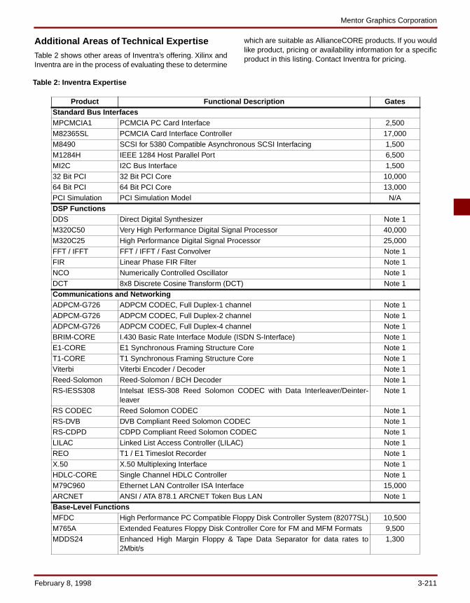
Mentor Graphics Corporation
Additional Areas of Technical ExpertiseTable 2 shows other areas of Inventra’s offering. Xilinx andInventra are in the process of evaluating these to determine
which are suitable as AllianceCORE products. If you wouldlike product, pricing or availability information for a specificproduct in this listing. Contact Inventra for pricing.
Product Functional Description GatesStandard Bus InterfacesMPCMCIA1 PCMCIA PC Card Interface 2,500M82365SL PCMCIA Card Interface Controller 17,000M8490 SCSI for 5380 Compatible Asynchronous SCSI Interfacing 1,500M1284H IEEE 1284 Host Parallel Port 6,500MI2C I2C Bus Interface 1,50032 Bit PCI 32 Bit PCI Core 10,00064 Bit PCI 64 Bit PCI Core 13,000PCI Simulation PCI Simulation Model N/ADSP FunctionsDDS Direct Digital Synthesizer Note 1M320C50 Very High Performance Digital Signal Processor 40,000M320C25 High Performance Digital Signal Processor 25,000FFT / IFFT FFT / IFFT / Fast Convolver Note 1FIR Linear Phase FIR Filter Note 1NCO Numerically Controlled Oscillator Note 1DCT 8x8 Discrete Cosine Transform (DCT) Note 1Communications and NetworkingADPCM-G726 ADPCM CODEC, Full Duplex-1 channel Note 1ADPCM-G726 ADPCM CODEC, Full Duplex-2 channel Note 1ADPCM-G726 ADPCM CODEC, Full Duplex-4 channel Note 1BRIM-CORE I.430 Basic Rate Interface Module (ISDN S-Interface) Note 1E1-CORE E1 Synchronous Framing Structure Core Note 1T1-CORE T1 Synchronous Framing Structure Core Note 1Viterbi Viterbi Encoder / Decoder Note 1Reed-Solomon Reed-Solomon / BCH Decoder Note 1RS-IESS308 Intelsat IESS-308 Reed Solomon CODEC with Data Interleaver/Deinter-
leaverNote 1
RS CODEC Reed Solomon CODEC Note 1RS-DVB DVB Compliant Reed Solomon CODEC Note 1RS-CDPD CDPD Compliant Reed Solomon CODEC Note 1LILAC Linked List Access Controller (LILAC) Note 1REO T1 / E1 Timeslot Recorder Note 1X.50 X.50 Multiplexing Interface Note 1HDLC-CORE Single Channel HDLC Controller Note 1M79C960 Ethernet LAN Controller ISA Interface 15,000ARCNET ANSI / ATA 878.1 ARCNET Token Bus LAN Note 1Base-Level FunctionsMFDC High Performance PC Compatible Floppy Disk Controller System (82077SL) 10,500M765A Extended Features Floppy Disk Controller Core for FM and MFM Formats 9,500MDDS24 Enhanced High Margin Floppy & Tape Data Separator for data rates to
2Mbit/s1,300
Table 2: Inventra Expertise
February 8, 1998 3-211
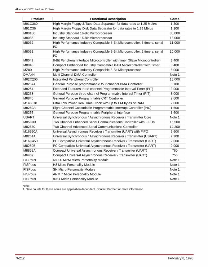
AllianceCORE Partner Profiles
Note: 1. Gate counts for these cores are application dependent. Contact Partner for more information.
M91C360 High Margin Floppy & Tape Data Separator for data rates to 1.25 Mbit/s 1,300M91C36 High Margin Floppy Disk Data Separator for data rates to 1.25 Mbit/s 1,100M80186 Industry Standard 16-Bit Microprocessor 30,000M8086 Industry Standard 16-Bit Microprocessor 18,000M8052 High Performance Industry Compatible 8-Bit Microcontroller, 3 timers, serial
I/O11,000
M8051 High Performance Industry Compatible 8-Bit Microcontroller, 2 timers, serialI/O
10,000
M8042 8-Bit Peripheral Interface Microcontroller with timer (Slave Microcontroller) 3,400M8048 Compact Embedded Industry Compatible 8-Bit Microcontroller with Timer 3,400MZ80 High Performance Industry Compatible 8-Bit Microprocessor 8,000DMAxN Multi Channel DMA Controller Note 1M82C206 Integrated Peripheral Controller 18,000M8237A General Purpose programmable four channel DMA Controller 3,700M8254 Extended Features three channel Programmable Interval Timer (PIT) 3,000M8253 General Purpose three channel Programmable Interval Timer (PIT) 3,000M6845 General Purpose Programmable CRT Controller 2,600M146818 Ultra Low Power Real Time Clock with up to 114 bytes of RAM 2,000M8259A Eight Channel Cascadable Programmable Interrupt Controller (PIC) 1,600M8255 General Purpose Programmable Peripheral Interface 1,600USART Universal Synchronous / Asynchronous Receiver / Transmitter Core Note 1M85C30 Two Channel Enhanced Serial Communications Controller with FIFOs 16,500M82530 Two Channel Advanced Serial Communications Controller 12,200M16550A Universal Asynchronous Receiver / Transmitter (UART) with FIFO 6,600M8251A Universal Synchronous / Asynchronous Receiver / Transmitter (USART) 2,200M16C450 PC Compatible Universal Asynchronous Receiver / Transmitter (UART) 2,000M8250B PC Compatible Universal Asynchronous Receiver / Transmitter (UART) 2,000M8868A Compact Universal Asynchronous Receiver / Transmitter (UART) 760M6402 Compact Universal Asynchronous Receiver / Transmitter (UART) 750FISPbus 68000 MPM Micro Personality Module Note 1FISPbus H8 Micro Personality Module Note 1FISPbus SH Micro Personality Module Note 1FISPbus ARM 7 Micro Personality Module Note 1FISPbus 8051 Micro Personality Module Note 1
Product Functional Description Gates
3-212 February 8, 1998
Partner Profile
February 8, 1998
Mobile Media Research, Inc.
39675 Cedar Boulevard, #295ANewark, CA 94560 USAPhone: +1 800 799-MMRI (6674)
+1 510 657-4891Fax: +1 510 657-4892E-mail: [email protected]: www.mobmedres.com
OverviewMobile Media Research was founded in 1991 with the mis-sion to provide complete solutions and enabling technologyfor the rapidly growing mobile computing market and spe-cifically the PCMCIA marketplace. Today, Mobile MediaResearch is the premier supplier of PC Card developmenttools and testing systems that drastically reduce time-to-market and increase productivity for Card and Host devel-opers. Simultaneously, Mobile Media Research is develop-ing a line of IP Cores for FPGA-based designs to enabledesigners to meet the challenges of increased design com-plexity and faster time-to-market. The company also offerslow cost design and consulting services in the areas ofcomputer connectivity standards, in particular PCMCIA andCardBus, Multimedia, communications, telecom, and net-working. Mobile Media Research will be offering cores forASIC-based designs in the future.
The SocketWareTM product line offers the best solution for16-bit PC Card product development and system testing. It
is a complete family of unique software and hardware prod-ucts that provide design solutions for the PCMCIA engi-neering community. Both hardware and softwaredevelopment tools are designed to accelerate design anddebug cycles, thus reducing time-to-market of PCMCIAproducts.
Mobile Media Research has recently introduced CBW-areTM, a complete line of CardBus development and testtools for the design of 32-bit CardBus hosts, cards, andapplications. The CardBus product line is aimed at provid-ing development solutions and building blocks that, like allMobile Media Research products will reduce developmenttime immensely and drastically cut time-to-market.
The IP Core family of SoftLogicTM is a diverse line of reus-able synthesizable macro functions designed specificallyfor FPGAs. The cores are customizable and can be useddirectly in the target device. Each core comes with all thenecessary documentation and test bench support toensure a quick and smooth integration into customerdesigns. Each core is verified for timing and functionality.The macro functions of the SoftLogic family are supportedwith optional prototyping boards, test software, and testbench modules.
AllianceCORE ProductsTable 1 shows AllianceCORE released products fromMobile Media Research Inc. Datasheets for these areincluded in the AllianceCORE Products section of thisdatabook. Contact Mobile Media Research for pricing.
Product Description DatasheetAllianceCORE Modules - Standard Bus InterfacesXilinx Fax/Modem Macro
A PCMCIA fax/modem interface for implementing a complete fax/modem card using an external fax/modem chipset.
3-15
Xilinx PCMCIA Library R1.2
A comprehensive library for developing PCMCIA compliant hardware prod-ucts with Xilinx FPGAs.
3-19
Supporting Development ToolsPCMCIA Prototyp-ing Card
A Xilinx-based configurable development platform for designing and debug-ging PC-Cards.
3-23
PCMCIA Card De-bugger/Exerciser
A fully-compatible, Microsoft Windows based PCMCIA debugger and exer-ciser for hardware and software development.
3-25
CIS Generator 1.2 This is a feature-rich, Windows-based compiler that automates the genera-tion of a PCMCIA-compatible CIS.
3-27
Table 1: Released AllianceCORE Products
February 8, 1998 3-213
AllianceCORE Partner Profiles
Additional Areas of Technical ExpertiseTable 2 shows other areas of Mobile Media Research tech-nical expertise. Xilinx and Mobile Media Research are inthe process of evaluating these to determine which are suit-
able as AllianceCORE products. If you have a need for aspecific product then contact MMRI for information or avail-ability.
Product Functional Description GatesStandard Bus Interfaces XFlash A complete Xilinx PCMCIA interface macro for Intel Series 2 compatible
Flash memory cards.HP-Pro Series Logic Analyzer/Extender Card
A highly sophisticated and versatile PCMCIA development tool. N/A
Type Converter Card
A uniquely designed PCMCIA type converter/socket saver that expands the mechanical capacity of host sockets.
N/A
CardTRAC A high-value, single slot AT/PCMCIA adapter that includes card & socket services and provides an ISA-based PCMCIA and JEIDA 4.1 platform.
N/A
PCIC Software Functions Library
An extensive library for developing PCMCIA compliant software products. N/A
CBWareTM Devel-opment Tools
A complete family of products for CardBus product development. N/A
CB Macro CardBus interface macro. N/ACBWareTM De-velopment Tools
A complete family of products for CardBus product development N/A
Base-Level FunctionsSDRAM Controller N/A
Table 2: Mobile Media Research Inc. Expertise
3-214 February 8, 1998
February 8, 1998 3-215
Partner Profile
NMI Electronics Ltd.
Fountain HouseGreat CornbowHalesowenWest MidlandsB63 3BL, UKPhone: +44 (0) 121 585 5979Fax: +44 (0) 121 585 5764E-mail: [email protected]: www.nmi.co.uk
OverviewNMI is an independent design services company and isnow making its expertise available in the form of IntellectualProperty cores via the Xilinx AllianceCORE program.These cores leverage NMI's skills, particularly in the area ofhigh speed digital design, to provide commonly requiredand easily customizable functions which are instantlyusable.
NMI cores mainly target the XC9500 family and will beavailable in optimized HDL source code. This allows thecores to provide the flexibility which many applicationsdemand. First time users will find that NMI’s cores acceler-ate their learning process, giving them the confidence torapidly move forward.
NMI also offers full product design services to customers.These range from modifying AllianceCORE offerings,through providing custom cores, to full core integration,system design and prototyping.
Table 1: Released AllianceCORE Products
NMI designs systems with diverse requirements: lowpower; high performance; low cost; ease of manufacture.We also have in-depth experience of PC hardware andsoftware development, including planar boards, PCI andPCMCIA.
NMI is dedicated to providing successful solutions to itscustomers' product design needs. Incorporated in 1987,NMI has very strong systems design skills, coupled withproven project management abilities. These ensure thatproduct developments are delivered on time and to budget.
Areas of Technical ExpertiseTable 1 lists areas of NMI Electronics’ technical expertise.Xilinx and NMI are in the process of evaluating these todetermine which are suitable as AllianceCORE products. Ifyou have a need for a specific product then contact NMI forinformation or availability.
Additional Areas of Technical ExpertiseTable 2 demonstrates other areas of NMI technical exper-tise. Xilinx and NMI are in the process of evaluating theseto determine which are suitable as AllianceCORE products.If you have a need for a specific product then contact NMIfor information or availability.
Table 2: NMI Expertise
Product Functional Description DatasheetBase-Level FunctionsDRAM Controller DRAM Controller for XC9500 3-173Supporting Development ToolsPrototyping Board Core Prototyping Board for Xilinx FPGAs and CPLDs 3-185
Product Functional Description GatesStandard Bus InterfacesI2C I2C Slave Interface for XC9500Base-Level FunctionsDRAM Controller DRAM Controller for the XC4000
February 8, 1998
3-216 February 8, 1998
Partner Profile
Perigee, LLC
314 Second StreetLiverpool, New York 13088 USAPhone +1 315 453-7842Fax: +1 315 453-7917E-mail: [email protected]: www.PerigeeLLC.com
OverviewPerigee, LLC is a technology company specializing in newproduct development. Perigee’s focus is electronic systemdesign, partitioning and development. We are committed toleveraging the ever-growing size of programmable logicwithout sacrificing time-to-market. To this goal, Perigeeoffers IP cores as well as customization, FPGA/CPLDdesign and integration services. Our design solutionsrange from proof of concept designs through final productsolutions.
Perigee offers services and contract engineering for vary-ing levels of development from logic design to system levelembedded and bus-based products. These servicesinclude:
• IC design, VHDL or schematic based• turnkey hardware/software/firmware development• system design • board design• DSP and image processing• Embedded firmware• GUI and Application software
Areas of ExpertiseThe following table of products demonstrates areas of Peri-gee technical expertise. Xilinx and Perigee are in the pro-cess of evaluating these to determine which are suitable asAllianceCORE products. If you have a need for a specificproduct then contact Perigee for information or availability.
Product Description Gates
DSP Functions
YCrCb to RGB YCrCb to RGB color space converter 4,000
RGB to YCrCb RGB to YCrCb color space converter 6,000
Gamma Corrector 2,000
Inverse Gamma Corrector 2,000
Active Matrix LCD controller 2-5,000
2-D Video Convolver
February 8, 1998
Table 1: Perigee Expertise
February 8, 1998 3-217
Partner Profile
Phoenix Technologies/Virtual Chips
411 E. Plumeria Drive San Jose, CA 95134 USAPhone: +1 408 570-1000 Fax: +1 408 570-1230 E-mail: [email protected] URL: www.phoenix.com
Overview The Virtual Chips division of Phoenix Technologies Ltd., isthe world’s leading supplier of synthesizable cores and testenvironments for computer connectivity standards includ-ing PCI, USB, CardBus, PCMCIA and AGP.
Using Virtual Chips products, design teams are able tobring leading edge, high performance ICs to market faster,with assured compliance to computer connectivity stan-dards. Each Virtual Chips product includes all the design
features, documentation guidance and support necessaryto ensure fast, smooth integration into customer designsand optimal results in silicon.
Phoenix Technologies Ltd. is headquartered in San Jose,CA, with sales, support and R&D facilities in Norwood, MA,Irvine, CA, Japan, Taiwan, France, and the U.K.
Areas of Technical Expertise Table 1 shows areas of Phoenix Technologies Ltd. technicalexpertise. Xilinx and Phoenix are in the process of evaluat-ing these to determine which are suitable as AllianceCOREproducts. If you have a need for a specific product then con-tact Phoenix Technologies Ltd. for information or availabil-ity.
* Exact gate count depends on product configuration.
Product Functional Description GatesStandard Bus Interfaces
Peripheral Component Interconnect (PCI) 7,000 + FIFO’s *
Universal Serial Bus (USB) 6,000 *Accelerated Graphics Port (AGP) 10,000 *CardBus Test Environment N/APCMCIA Test Environment N/A
February 8, 1998
Table 1: Phoenix Technology Expertise
Partner Profile
February 8, 1998
RICE
Rice Electronics PO Box 741 Florissant, MO 63032 USA Phone: +1 314 838-2942 Fax: +1 314 838-2942 E-mail: [email protected]
Overview Rice Electronics provides cores for FPGA-based designs.The cores range from multipliers to Discrete Fourier Trans-forms (DFTs), and are targeted at the Xilinx XC4000E logicfamily.
Rice Electronics employs a variety of proprietary tech-niques to reduce DSP circuit complexity. These range fromspecialized architectures, to highly efficient algorithms.This results in cores which rival the performance of stan-dard DSP components.
The XACTstep 6.0 development system provides the envi-ronment for application of the cores. The current focus is onDFT/FFT functions, with additional cores being planned.
Additional Areas of Technical Expertise Table 1 shows areas of Rice Electronics’ technical exper-tise. Xilinx and Rice are in the process of evaluating theseto determine which are suitable as AllianceCORE products.If you have a need for a specific product then contact Ricefor information or availability.
Product Functional Description GatesDSP FunctionsFFTs and DFTs DSP Modules for Xilinx XC4000 Family Devices
Table 1: Rice Technology Expertise
3-218 February 8, 1998
Partner Profile
February 8, 1998
Sand Microelectronics
2121 Ringwood DriveMilpitas, CA 95131 USA Phone: +1 408 235-8600 Fax: +1 408 235-6801 E-mail: [email protected] URL: www.sandmicro.com
Overview Sand Microelectronics provides productivity tools for FPGAand ASIC designers, including Verilog/VHDL simulationmodels and synthesizable cores, enabling designers toreduce product development time and improve design qual-ity.
Sand Microelectronics’ cores are fully synthesizable andsilicon-proven. Each core can easily be migrated to almostany ASIC/FPGA technology in a relatively short period oftime. Using Sand’s RapidScript Utility , the cores can bequickly configured to match the needs of the user’s applica-tion. By utilizing Sand’s tested cores, designers can signifi-
cantly reduce development time and engineering risk andbring their products to market faster.
Sand Microelectronic’s PCI Synthesizable Core is a set ofsynthesizable building blocks that ASIC and FPGA design-ers can use to implement a complete PCI interface. ThePCI Core contains all the necessary hooks for customizingand optimizing it for a specific application.
Sand’s also provides Universal Serial Bus (USB), Hub andHost controller cores that are fully synthesizable and inter-gratable in FPGAs or ASICs. Sand also supplies bus func-tional simulation models and a USB Transaction Analysistool for USB verification.
Additional Areas of Technical Expertise Table 1 shows areas of Sand Microelectronics’ technicalexpertise. Xilinx and Sand are in the process of evaluatingthese to determine which are suitable as AllianceCOREproducts. If you have a need for a specific product then con-tact Sand for information or availability.
.
Product Functional Description GatesStandard Bus InterfacesPCI 32bit/33 MHzPCI 64bit/33 MHzPCI 32bit/ 66MHzPCI 64bit/66 MHz
Systhesizable PCI cores, fully Revision 2.1 compliant; bridges PCI to high performance F-Bus (FIFO Bus). Design is synchronous to PCI clock, how-ever, F-Bus interface to a specific peripheral need not be synchronous. RapidScript Utility configurable to match an application’s interface re-quirements.
USB Device Controller (UDC)
General purpose solution for USB peripheral devices. Quickly configured for any number of End-Points using RapidScript. Does not require a micro-controller or firmware.
5,000
USB Hub Controller
RapidScript configurable, does not require a microcontroller or firmware.
Table 1: Sand Microelectronics Expertise
February 8, 1998 3-219
3-220 February 8, 1998
Partner Profile
SICAN Microelectronics Corp.
400 Oyster Point Blvd., Suite 512South San Francisco, CA 94080 USAPhone: +1 650 871-1494Fax: +1 650 871-1504E-mail: [email protected]: www.sican-micro.com
SICAN GmbHGarbsener Landstrasse 10HannoverD-30419, GermanyPhone: +(49)511-277-1601Fax: +(49)511-277-2600URL: www.sican.de
OverviewSICAN GmbH, headquartered in Hannover, Germany, is amicroelectronics design company specializing in communi-cations, multimedia and networking applications. Its techni-cal staff and infrastructure form an organization with theflexibility and innovation to meet the rapidly changingdesign needs of its customers.
As a full-service design house, SICAN functions like otherAmerican design houses, offering IC development ser-vices. The company has expertise in classical ASIC devel-opment using gate array and standard cell architectures. Ithas over 200 designs which have been implemented in var-ious companies and acts as an authorized design center forseveral world-class ASIC vendors.
SICAN has developed advanced core expertise in topicssuch as MPEG video and audio encoding and decoding,high-speed networking, broadband media access, andmixed-signal design. SICAN's intellectual property isaggregated in cores called DesignObjectsTM, are licensedto companies creating systems-on-silicon. It also has astaff of over 300 employees, making it one of the largestindependent design houses which licenses its intellectualproperty. This impressive design force allows SICAN tooffer the highest quality, customer specific designs as wellas reduce their time-to-market.
Areas of Technical ExpertiseTable 1 shows SICAN Microelectronics areas of technicalexpertise. Xilinx and SICAN are in the process of evaluat-ing these to determine which are suitable as AllianceCOREproducts. If you have a need for a specific product then con-tact SICAN for information or availability.
Product Functional Description GatesStandard Bus InterfacesCAN Bus Module CAN Bus interface module.IIC Slave Interface IIC Slave InterfaceDSP FunctionsDES Data Encryption Standard (DES)Communications and NetworkingHDLC HDLC
Reed-Solomon DecoderUTOPIA UTOPIA InterfaceBase-Level Functions
Pulse-Width Modulator
February 8, 1998
Table 1: SICAN Expertise

February 8, 1998 3-221
Partner Profile
T7L Technology, Inc.220 Duncanmill RoadSuite 307North York, OntarioCanada, M3B 3J5Phone: +1 416-445-4783Fax: +1 416-445-5741E-mail: [email protected]: www.t7l.com
OverviewT7L Technology is a leading provider of VHDL based syn-thesizable processor cores for FPGA and ASIC customers.The main advantage of using T7L products are producttime-to-market and design optimization. With these cores,users can significantly reduce product design cycles andgain market leadership advantages.
Design optimization also ensures that real time perfor-mance can be achieved. High optimization in silicon areawill minimize power consumption. With large gate count
FPGAs available today, embedded CPU cores becomes anessential element for today's applications.
Based on its proprietary scaleable RISC architecture, T7Lhas built a family of 26 CPU cores optimized for XilinxXC4000 series FPGA devices. It is built around a 3-stagepipeline engine with separated instruction and data buses.A flexible and selectable instruction set can be extractedfrom a supplied master function library. Parameter-drivenconfigurable design allows fast and easy customization.This is the first RISC CPU core dedicated for FPGA appli-cation.
Areas of Technical ExpertiseTable 1 lists areas of T7L Technology’s technical expertise.Xilinx and T7L are in the process of evaluating these todetermine which are suitable as AllianceCORE products. Ifyou have a need for a specific product then contact T7LTechnology for information or availability.
Product Functional Description DatasheetBase Level FunctionsTX400 FPGA optimized RISC processor core family 3-97Design Base Board
Xilinx FPGA-based hardware development board for TX400 RISC CPU cores
3-103
SDP Integrated Software
Complete Windows '95 based integrated development environment for TX400 CPU cores
3-107
February 8, 1998
Table 1: Released AllianceCORE Products
3-222 February 8, 1998
Partner Profile
Technology Rendezvous Inc.
3160 De La Cruz Blvd. #101Santa Clara, CA 95054 USAPhone: +1 408 566-0280Fax: +1 408 566-0284E-mail: [email protected]: www.trinc.com
OverviewTechnology Rendezvous Inc. (TRI) is focused on theembedded systems, bus interface and networking markets.TRI provides time and cost effective system solutions(hardware and software), design services and system levelmacros including synthesizable logic cores (softcores) andverification models to FPGA/ASIC designers. Our profes-sional services division provides customized solutions inthe design and development of software and hardware.
TRI believes in providing complete solutions for systemdesigns. Apart from supplying generic Logic Cores, TRIalso provides additional tools such as drivers, system soft-ware for Embedded Systems and prototyping systems.These solutions help the designers to rapidly integrate thecore into their ASIC designs, perform system debug in a
real-world environment, and then quickly convert the proto-type to a production unit. In the area of Embedded SystemsTRI has expertise in providing systems solutions, BSPsand drivers for the embedded systems running real timeOS like pSOS, VxWorks etc.
TRIs IEEE-1394 (Firewire) Synthesizable Core is a build-ing block that ASIC and FPGA designers can use to imple-ment a complete 1394 interface. In addition to the core, TRIis currently developing an FPGA based 1394 host andperipheral emulation system. This emulation system is anideal platform for 1394 developers to prototype their hard-ware, firmware and software stack.
Areas of Technical ExpertiseTable 1 shows areas of Technology Rendezvous Inc. tech-nical expertise. Xilinx and TRI are in the process of evaluat-ing these to determine which are suitable as AllianceCOREproducts. If you have a need for a specific product then con-tact Technology Rendezvous Inc. for information or avail-ability.
Table 1: Technology Rendezvous Inc. Expertise
Product Functional Description Gates Standard Bus Interfaces FireWire Core The core has two components: Link Layer & OHCI Layer; fully compliant
with IEEE-1394-1995bus standard specifications; contains all necessary hooks for customizing and optimizing it for a specific application
February 8, 1998
Partner Profile
February 8, 1998
VAutomation
20 Trafalgar Square Suite 443 (4th Floor) Nashua NH 03063 USA Phone: +1 603 882-2282 Fax: +1 603 882-1587 E-mail: [email protected] URL: www.vautomation.com
OverviewVAutomation was one of the first companies to recognizethe need for re-usable intellectual property (IP) – or cores –when designing with ASICs and FPGAs. Since 1994, it hasprovided synthesizable HDL-based cores for microproces-sors and serial communications controllers. VAutomationpre-designed and verified cores allow microprocessors andserial communications controllers, the 8086 and UniversalSerial Bus for example, to be implemented within an ASICor FPGA for true system-on-chip design.
Our cores are strictly synchronous making them easy tosynthesize to any technology. Synthesis and timing analy-sis are simple, push-button operations with the samplescripts provided with each core. A comprehensive test-bench is also provided for design verification and functionaltest vector extraction.
All of our cores have been thoroughly verified in siliconusing Xilinx FPGA technology. Evaluation silicon is avail-able for evaluating our cores and to enable early software/hardware integration. The V8-uRISC 8-bit RISC micropro-
cessor and VUSB Universal Serial Bus Microcontrollercores are supported via the IntelliCore Prototyping System.This system, based on one to four XC4028 FPGAS, allowsour cores and user logic to be easily prototyped anddebugged.
VAutomation is exclusively focused on providing synthesiz-able cores. We market and sell our products through adirect sales and support operation headquartered inNashua, N.H. The company is privately held with seedfunding provided by its founders.
Areas of Technical ExpertiseTable 1 lists areas of VAutomation’s technical expertise. Xil-inx and VAutomation are in the process of evaluating theseto determine which are suitable as AllianceCORE products.If you have a need for a specific product then contact VAu-tomation for information or availability.
Additional Areas of Technical ExpertiseTable 2 shows areas of VAutomation’s technical expertise.Xilinx and VAutomation are in the process of evaluatingthese to determine which are suitable as AllianceCOREproducts. If you have a need for a specific product then con-tact VAutomation for information or availability.
Product Functional Description DatasheetBase Level FunctionsV8 uRISC 8-bit FPGA-based RISC processor 3-109Supporting Development ToolsProto Board IntelliCoreTM prototyping System - Xilinx FPGA based prototype and core
evaluation board for the V8 uRISC and other VAutomation cores.3-115
Table 1: Released AllianceCORE Products
February 8, 1998 3-223
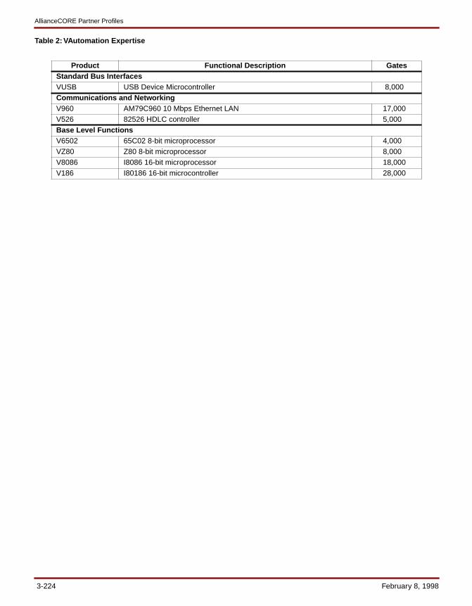
AllianceCORE Partner Profiles
Product Functional Description GatesStandard Bus InterfacesVUSB USB Device Microcontroller 8,000Communications and NetworkingV960 AM79C960 10 Mbps Ethernet LAN 17,000V526 82526 HDLC controller 5,000Base Level FunctionsV6502 65C02 8-bit microprocessor 4,000VZ80 Z80 8-bit microprocessor 8,000V8086 I8086 16-bit microprocessor 18,000V186 I80186 16-bit microcontroller 28,000
Table 2: VAutomation Expertise
3-224 February 8, 1998
February 8, 1998 3-225
Partner Profile
Virtual IP Group, Inc.
1094 E. Duane Ave., Suite 211 Sunnyvale, CA 94086 USAPhone: +1 408 733-3344Fax: +1 408 733-9922E-mail: [email protected] : www.virtualipgroup.com
Overview Virtual IP Group, Inc. is a leading provider of Verilog HDLsynthesizable industry-standard cores for FPGAs andASICs.
Virtual IP Group is equipped with state-of-the-art hardwareand software, and over thirty talented engineers with exten-sive backgrounds in system and ASIC design. This allowsVirtual IP to offer quality products with superb documenta-tion in time to meet critical product schedules. All cores areclean room designed and proven in silicon.
Virtual IP Group offers synthesizable cores for microcon-trollers (8031 and PIC family), telecommunication (E1/T1framers, muxs etc.), datacom, PC peripherals and businterface standards. Virtual IP Group also provides ASIC
services including custom library creation. Virtual IP Grouphas optimized some of these cores for use in Xilinx FPGAs.Virtual IP Group will also be offering DSP and analog coresin the future. Contact Virtual IP Group directly for the latestproduct offering.
AllianceCORE ProductsTable 1 shows AllianceCORE products available from theVirtual IP Group. Datasheets for these are included in theAllianceCORE Products section of this databook. ContactVirtual IP Group for pricing
Additional Areas of Technical ExpertiseTable 2 demonstrates other areas of Virtual IP Group tech-nical expertise. Xilinx and Virtual IP Group are in the pro-cess of evaluating these to determine which are suitable asAllianceCORE products. If you have a need for a specificproduct then contact Virtual IP Group for information oravailability.
Table 1: Released AllianceCORE Products
Product Description DatasheetCommunications and NetworkingMT1F T1 Framer 3-81Base Level FunctionsM8237 Programmable DMA Controller 3-133M8254 Programmable Interval Timer 3-143M8255 Programmable Peripheral Interface 3-147M8259 Programmable Interrupt Controller 3-159M16450 UART 3-121M16550A UART + FIFO 3-125
February 8, 1998
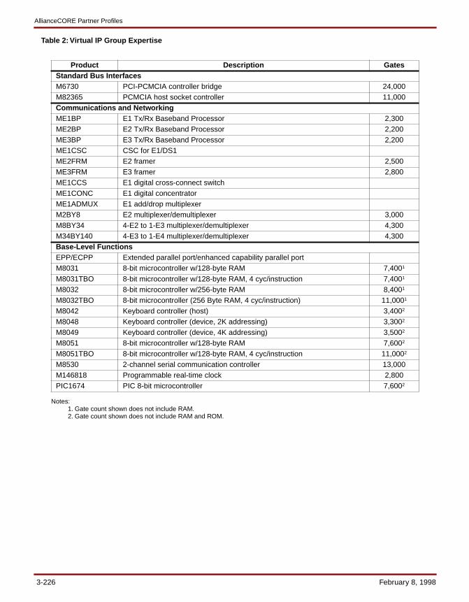
AllianceCORE Partner Profiles
3-226 February 8, 1998
Notes:1. Gate count shown does not include RAM.2. Gate count shown does not include RAM and ROM.
Product Description Gates Standard Bus InterfacesM6730 PCI-PCMCIA controller bridge 24,000M82365 PCMCIA host socket controller 11,000Communications and NetworkingME1BP E1 Tx/Rx Baseband Processor 2,300ME2BP E2 Tx/Rx Baseband Processor 2,200ME3BP E3 Tx/Rx Baseband Processor 2,200ME1CSC CSC for E1/DS1ME2FRM E2 framer 2,500ME3FRM E3 framer 2,800ME1CCS E1 digital cross-connect switchME1CONC E1 digital concentratorME1ADMUX E1 add/drop multiplexerM2BY8 E2 multiplexer/demultiplexer 3,000M8BY34 4-E2 to 1-E3 multiplexer/demultiplexer 4,300M34BY140 4-E3 to 1-E4 multiplexer/demultiplexer 4,300Base-Level FunctionsEPP/ECPP Extended parallel port/enhanced capability parallel portM8031 8-bit microcontroller w/128-byte RAM 7,4001
M8031TBO 8-bit microcontroller w/128-byte RAM, 4 cyc/instruction 7,4001
M8032 8-bit microcontroller w/256-byte RAM 8,4001
M8032TBO 8-bit microcontroller (256 Byte RAM, 4 cyc/instruction) 11,0001
M8042 Keyboard controller (host) 3,4002
M8048 Keyboard controller (device, 2K addressing) 3,3002
M8049 Keyboard controller (device, 4K addressing) 3,5002
M8051 8-bit microcontroller w/128-byte RAM 7,6002
M8051TBO 8-bit microcontroller w/128-byte RAM, 4 cyc/instruction 11,0002
M8530 2-channel serial communication controller 13,000M146818 Programmable real-time clock 2,800 PIC1674 PIC 8-bit microcontroller 7,6002
Table 2: Virtual IP Group Expertise
R LogiBLOX
1. Introduction
2. LogiCORE Products
3. AllianceCORE Products
4. LogiBLOX
5. Reference Designs
4-1
R LogiBLOX Table of Contents
February 8, 1998
LogiBLOXLogiBLOX . . . . . . . . . . . . . . . . . . . . . . . . . . . . . . . . . . . . . . . . . . . . . . . . . . . . . . . . . . . .4-3
4-2 February 8, 1998
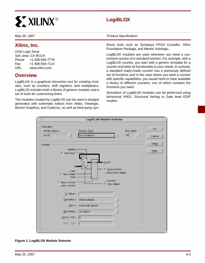
R
May 25, 1997 Product Specification
LogiBLOX
Xilinx, Inc.2100 Logic DriveSan Jose, CA 95124Phone +1 408-559-7778Fax: +1 408-559-7114URL www.xilinx.com
OverviewLogiBLOX is a graphical interactive tool for creating mod-ules, such as counters, shift registers, and multiplexers.LogiBLOX includes both a library of generic modules and aset of tools for customizing them.
The modules created by LogiBLOX can be used in designsgenerated with schematic editors from Aldec, Viewlogic,Mentor Graphics, and Cadence, as well as third-party syn-
thesis tools such as Synopsys FPGA Compiler, XilinxFoundation Package, and Mentor Autologic.
LogiBLOX modules are used whenever you need a cus-tomized version of a standard function. For example, with aLogiBLOX counter, you start with a generic template for acounter and tailor its functionality to your needs. In contrast,a standard ready-made counter has a previously definedset of functions and in the case where you want a counterwith specific capabilities, you would need to have availablea library of different counters, one of which contains thefunctions you need.
Simulation of LogiBLOX modules can be performed usingbehavioral VHDL, Structural Verilog or Gate level EDIFmodels.
Figure 1. LogiBLOX Module Selector
May 25, 1997 4-3
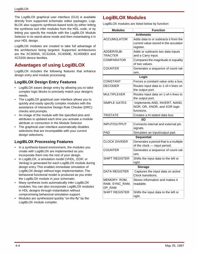
LogiBLOX
The LogiBLOX graphical user interface (GUI) is availabledirectly from supported schematic editor packages. Logi-BLOX also supports synthesis-based tools by either lettingthe synthesis tool infer modules from the HDL code, or byletting you specify the module with the LogiBLOX ModuleSelector in its stand-alone mode and then instantiating it inyour HDL design.
LogiBLOX modules are created to take full advantage ofthe architecture being targeted. Supported architecturesare the XC3000A, XC3100A, XC4000E, XC4000EX andXC5200 device families.
Advantages of using LogiBLOXLogiBLOX includes the following features that enhancedesign entry and module processing:
LogiBLOX Design Entry Features• LogiBLOX eases design entry by allowing you to tailor
complex logic blocks to precisely match your design’s needs.
• The LogiBLOX graphical user interface allows you to quickly and easily specify complex modules with the assistance of interactive Design Rule Checker (DRC) checks and prompts.
• An image of the module with the specified pins and attributes is updated each time you activate a module attribute or connection in the Module Selector.
• The graphical user interface automatically disables selections that are incompatible with your current design selections.
LogiBLOX Processing Features• In a synthesis-based environment, the modules you
create with LogiBLOX are implemented as you incorporate them into the rest of your design.
• In LogiBLOX, a simulation model (VHDL, EDIF, or Verilog) is generated for each LogiBLOX module during design entry. This enables immediate simulation of LogiBLOX design without logic implementation. The behavioral functional model is produced as you enter the LogiBLOX module in your schematic.
• Many synthesis tools automatically infer LogiBLOX modules. You can also incorporate LogiBLOX modules in HDL designs through instantiation without compromising behavioral simulation support.
• Modules are synthesized quickly “on-the-fly” by the LogiBLOX module compiler.
LogiBLOX ModulesLogiBLOX modules are listed below by function:
Modules FunctionArithmetic
ACCUMULATOR Adds data to or subtracts it from the current value stored in the acculator register.
ADDER/SUB-TRACTER
Adds or subtracts two data inputs and a Carry input.
COMPARATOR Compares the magnitude or equality of two values.
COUNTER Generates a sequence of count val-ues.
LogicCONSTANT Forces a constant value onto a bus.DECODER Routes input data to 1-of-n lines on
the output port.MULTIPLEXER Routes input data on 1-of-n lines to
the output port.SIMPLE GATES Implements AND, INVERT, NAND,
NOR, OR, XNOR, and XOR logic functions.
TRISTATE Creates a tri-stated data bus.I/O
INPUT/OUTPUT Connects internal and external pin signals.
PAD Simulates an input/output pad. Sequential
CLOCK DIVIDER Generates a period that is a multiple of the clock — input period.
COUNTER Generates a sequence of count val-ues.
SHIFT REGISTER Shifts the input data to the left or right.
StorageDATA REGISTER Captures the input data on active
Clock transitions.MEMORY: ROM, RAM, SYNC_RAM, DP_RAM
Stores information and makes it readable.
SHIFT REGISTER Shifts the input data to the left or right.
4-4 May 25, 1997
R Reference Designs
1. Introduction
2. LogiCORE Products
3. AllianceCORE Products
4. LogiBLOX
5. Reference Designs
5-1
R Reference Designs Table of Contents
February 8, 1998
Reference DesignsReference Designs . . . . . . . . . . . . . . . . . . . . . . . . . . . . . . . . . . . . . . . . . . . . . . . . . . . . .5-3
5-2 February 8, 1998
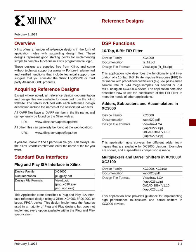
R
Reference Designs
February 8,1998
OverviewXilinx offers a number of reference designs in the form ofapplication notes with supporting design files. Thesedesigns represent good starting points for implementingsimple to complex functions in Xilinx programmable logic.
These designs are supplied free from Xilinx, and comewithout technical support or warranty. For pre-implementedand verified functions that include technical support, wesuggest that you consider the Xilinx LogiCORE or thirdparty AllianceCORE products.
Acquiring Reference DesignsExcept where noted, all reference design documentationand design files are available for download from the Xilinxwebsite. The tables included with each reference designdescription include the names of the associated web files.
All XAPP files have an XAPP number in the file name, andcan generally be found on the Xilinx web at:
URL: www.xilinx.com/apps/xapp.htm
All other files can generally be found at the web location:
URL: www.xilinx.com/apps/fpga.htm
If you are unable to find a particular file, you can always usethe Xilinx SmartSearchTM and enter the name of the file youwant.
Standard Bus Interfaces
Plug and Play ISA Interface in Xilinx
This Application Note describes a Plug and Play ISA inter-face reference design using a Xilinx XC4003-6PQ100C, orlarger, FPGA device. This design implements the featuresused in a majority of Plug and Play designs but does notimplement every option available within the Plug and Playspecification.
DSP Functions
16-Tap, 8-Bit FIR Filter
This application note describes the functionality and inte-gration of a 16-Tap, 8-Bit Finite Impulse Response (FIR) fil-ter macro with predefined coefficients (e.g. low pass) and asample rate of 5.44 mega-samples per second or 784MIPS using an XC4000-4 device. The application note alsodescribes how to set the coefficients of the FIR Filter tomeet the needs of other applications.
Adders, Subtracters and Accumulators in XC3000
This application note surveys the different adder tech-niques that are available for XC3000 designs. Examplesare shown, and a speed/size comparison is made.
Multiplexers and Barrel Shifters in XC3000/XC3100
This application note provides guidance for implementinghigh performance multiplexers and barrel shifters inXC3000 devices.
Device Family XC4000Documentation plugplay.pdfDesign File Formats ViewLogic
(pnp_v090.exepnp_upd.exe)
Device Family XC4000Documentation fir_filt.pdfDesign File Formats ViewLogic (fir_filt.zip)
Device Family XC3000Documentation xapp022.pdfDesign File Formats ViewdrawLCA
(xapp022v.zip)OrCAD 386+ V1.10(xapp022o.zip)
Device Family XC3000, XC3100Documentation xapp026.pdfDesign File Formats Viewdraw-LCA
(xapp026v.zip)OrCAD 386+ V1.10 (xapp026o.zip)
February 8,1998 5-3
Reference Designs
Base-Level Functions
Dynamic Microcontroller in XC4000
An application note and design files for a microcontrollerwith dynamic bus sizing. Uses Xilinx X-BLOX. A QBASIC-based assembler is available.
Loadable Binary Counters
The design strategies for loadable and non-loadable binarycounters are significantly different. This application notediscusses the differences, and describes the design of aloadable binary counter. Up, down and up/down countersare described, with lengths of 16 and 32 bits. Design filesare available for all six versions.
Ultra-Fast Synchronous Counters
This fully synchronous, non-loadable, binary counter usesa traditional prescaler technique to achieve high perfor-mance. Typically, the speed of a synchronous prescalercounter is limited by the delay incurred distributing the par-allel Count Enable. This design minimizes that delay by rep-licating the LSB of the counter. In this way even the smallLongline delay is eliminated, resulting in the fastest possi-ble synchronous counter.
Accelerating Loadable Counters in XC4000
The XC4000 dedicated carry logic provides for very com-pact, high-performance counters. This Application Notedescribes a technique for increasing the performance ofthese counters using minimum additional logic. Using thistechnique, the counters remain loadable.
Implementing FIFOs in XC4000 Series RAM
This application note demonstrates how to use the variousRAM modes in XC4000-Series logic blocks. A simple FIFOis implemented in several different ways, using combina-tions of level-sensitive (asynchronous) and edge-triggered(synchronous), single-port and dual-port RAM.
Register-Based FIFO
While XC3000-series LCA devices do not provide RAM, itis possible to construct small register-based FIFOs. A basicsynchronous FIFO requires one CLB for each two bits ofFIFO capacity, plus one CLB for each word in the FIFO.Optional asynchronous input and output circuits are pro-vided. Design files are available for two implementations ofthis design. The fastest of the two implementations uses aconstraints file to achieve better placement.
Device Family XC4000Documentation microcnt.pdfFile Formats ViewLogic (psmfiles.exe)
Device Family XC3000Documentation xapp004.pdfDesign File Formats Viewdraw-LCA
(xapp004v.zip)OrCAD 386+ V1.10 (xapp004o.zip)
Device Family XC3000, XC4000Documentation xapp014.pdfDesign File Formats Viewdraw-LCA
(xapp014v.zip)OrCAD 386+ V1.10 (xapp014o.zip)
Device Family XC4000Documentation xapp023.pdfDesign File Formats Viewdraw-LCA
(xapp023v.zip)OrCAD 386+ V1.10 (xapp023o.zip)
Device Family XC4000Documentation xapp053.pdfDesign Files Xilinx Web
Xilinx Literature (PCI Pack-et)
File Formats ViewLogic (xapp053v.zip)
Device Family XC3000Documentation xapp005.pdfDesign File Formats Viewdraw-LCA
(xapp005v.zip)OrCAD 386+ V1.10 (xapp005o.zip)
5-4 February 8,1998
Pulse-Width Modulation in Xilinx
An application note and design files for building a pulse-width modulation circuit in Xilinx programmable logic. UsesXilinx X-BLOX.
4Mbit Virtual SPROM
This application note describes the design of a very lowcost, CPLD-based virtual SPROM downloader for program-ming the Xilinx high-density XC4000-Series FPGAs inembedded applications.
Harmonic Frequency Synthesizer and FSK Modulator
The Harmonic Frequency Synthesizer uses an accumula-tor technique to generate frequencies that are evenlyspaced harmonics of some minimum frequency. Extensivepipelining is employed to permit high clock rates.
The FSK Modulator is a modification of the Harmonic Fre-quency Synthesizer that automatically switches betweentwo frequencies in accordance with an NRZ input.
Frequency/Phase Comparator for Phase-Locked Loops
The phase comparator described in this application notepermits phase-locked loops to be constructed using LCAdevices that only require an external voltage-controlledoscillator and integrating amplifier.
Serial Code Conversion Between BCD and Binary
Binary-to-BCD and BCD-to-binary conversions are per-formed between serial binary values and parallel BCD val-ues.
Configuring FPGAs Over a Processor Bus
This application note describes how to configure an SRAM-based FPGA over a processor bus. It also illustrates thesource code required to download a configuration bit-stream using an IBM PC as a host microprocessor.'C'source code is provided. Useful in reconfigurable comput-ing applications.
Device Family XC3000, XC4000, XC5000Documentation pwm.pdfDesign File Formats ViewLogic (pwm.zip)
Device Family XC9500Documentation xapp079.pdfDesign File Formats vsprom.zip
Device Family XC3000, XC4000Documentation xapp009.pdfDesign File Formats Viewdraw-LCA
(xapp009v.zip)OrCAD 386+ V1.10 (xapp009o.zip)
Device Family XC3000, XC4000, XC5000Documentation xapp028.pdfDesign File Formats Viewdraw-LCA
(xapp028v.zip)OrCAD 386+ V1.10 (xapp028o.zip)
Device Family XC3000Documentation xapp029.pdfDesign File Formats Viewdraw-LCA
(xapp029v.zip)OrCAD 386+ V1.10 (xapp029o.zip)
Device Family XC3000, XC4000, XC5000Documentation bus_conf.pdfDesign File Formats ViewLogic and C source
code: pc_isa.zip
February 8,1998 5-5