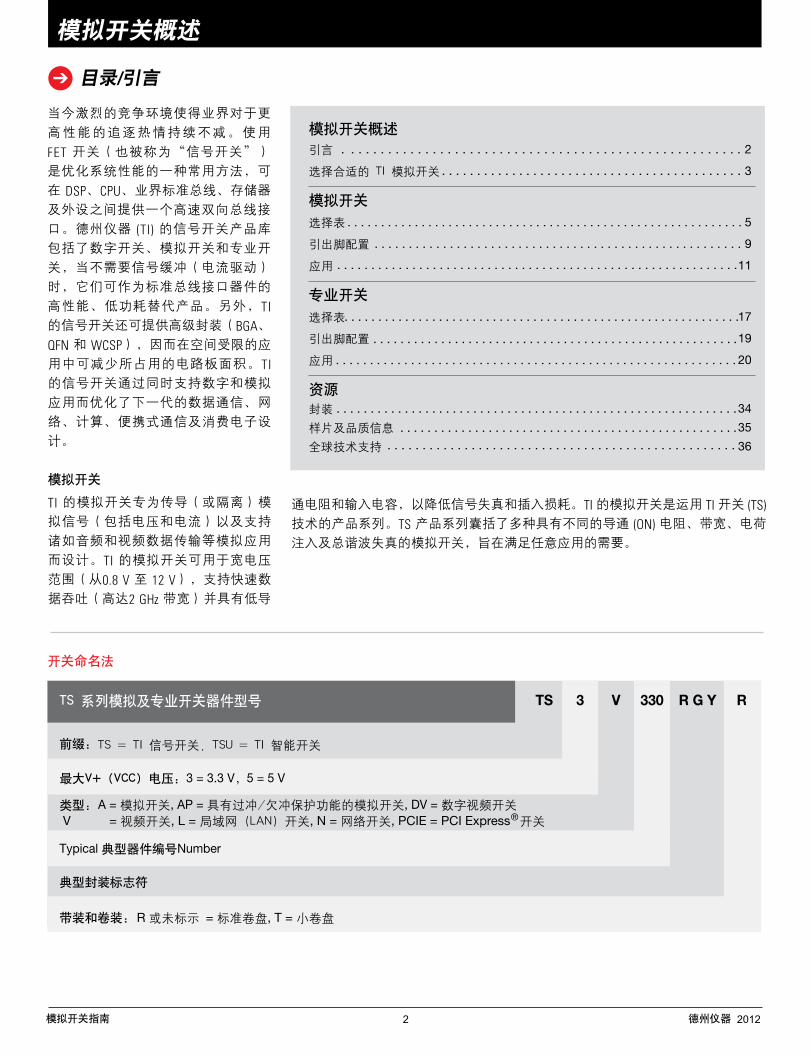
模拟开关指南 - 世纪电源网
TRANSCRIPT
2012www.ti.com.cn/switches
模拟开关指南
TI 信号开关产品线包括高性能、低功耗的数字、模拟及专业开关。
2Analog Switch Guide Texas Instruments 2012
TS 3 V 330 R G Y RTS-Series Analog and Speciality Switch Part Numbers
Prefix: TS = TI Signal switch, TSU = TI Smart switch
Max V+ (VCC) Voltage: 3 = 3.3 V, 5 = 5 V
Typical Device Number
Typical Package Designator
Tape and Reel: R or none = standard reel, T = small reel
Type: A = Analog switch, AP = Analog switch with over/undershoot protection, DV = Digital video switch V = Video switch, L = LAN switch, N = Network switch, PCIE = PCI Express® switch
Switch Nomenclature
Analog Switch Overview
Table of Contents / Introduction
Analog Switch OverviewIntroduction . . . . . . . . . . . . . . . . . . . . . . . . . . . . . . . . . . . . . . . . . . . . . . . . . . . . . . 2
Selecting the Right TI Analog Switch . . . . . . . . . . . . . . . . . . . . . . . . . . . . . . . . . . . 3
Analog SwitchesSelection Tables . . . . . . . . . . . . . . . . . . . . . . . . . . . . . . . . . . . . . . . . . . . . . . . . . . . 5
Pinouts . . . . . . . . . . . . . . . . . . . . . . . . . . . . . . . . . . . . . . . . . . . . . . . . . . . . . . . . . . 9
Applications . . . . . . . . . . . . . . . . . . . . . . . . . . . . . . . . . . . . . . . . . . . . . . . . . . . . . 11
Specialty SwitchesSelection Tables . . . . . . . . . . . . . . . . . . . . . . . . . . . . . . . . . . . . . . . . . . . . . . . . . . 17
Pinouts . . . . . . . . . . . . . . . . . . . . . . . . . . . . . . . . . . . . . . . . . . . . . . . . . . . . . . . . . 19
Applications . . . . . . . . . . . . . . . . . . . . . . . . . . . . . . . . . . . . . . . . . . . . . . . . . . . . . 20
Resources Packages . . . . . . . . . . . . . . . . . . . . . . . . . . . . . . . . . . . . . . . . . . . . . . . . . . . . . . . 34
Sample and Quality Information. . . . . . . . . . . . . . . . . . . . . . . . . . . . . . . . . . . . . . 35
Worldwide Technical Support. . . . . . . . . . . . . . . . . . . . . . . . . . . . . . . . . . . . . . . . 36
Today’s competitive environment creates a constant need for higher performance. One common method to optimize system performance involves the use of FET switches (also referred to as signal switches) to provide a high-speed bidirectional bus interface between DSPs, CPUs, industry stan-dard buses, memory and peripherals. The Texas Instruments (TI) signal switch product portfolio consists of digital switches, analog switches and specialty switches that provide high-performance, low-power replacements for standard bus-interface devices when signal buffering (current drive) is not required. Availability in advanced packaging (BGA, QFN and WCSP) also allows TI signal switches to occupy reduced board area in space-constrained applications. TI signal switches optimize next-generation datacom, networking, computing, portable communications and consumer electronic designs by supporting both digital and analog applications.
Analog Switches
TI’s analog switches are designed to pass (or isolate) analog signals (both voltage and current) and support
analog applications such as audio and video data transmission. TI analog switches are available in a wide range of voltages (from 0.8 to 12 V), support fast data through-put (up to 2-GHz bandwidth) and offer low on-resistance and input capacitance for decreased signal distortion and insertion loss. TI analog switches are available in the TI Switch (TS) technology family. The TS product family encompasses a variety of analog switches with different ON resistances, bandwidth, charge injection, and total harmonic distortion to target any application.
当今激烈的竞争环境使得业界对于更高性能的追逐热情持续不减。使用 FET 开关(也被称为“信号开关”)是优化系统性能的一种常用方法,可在 DSP、CPU、业界标准总线、存储器及外设之间提供一个高速双向总线接口。德州仪器 (TI) 的信号开关产品库包括了数字开关、模拟开关和专业开关,当不需要信号缓冲(电流驱动)时,它们可作为标准总线接口器件的高性能、低功耗替代产品。另外,TI 的信号开关还可提供高级封装(BGA、
QFN 和 WCSP),因而在空间受限的应用中可减少所占用的电路板面积。TI 的信号开关通过同时支持数字和模拟应用而优化了下一代的数据通信、网络、计算、便携式通信及消费电子设计。
模拟开关
TI 的模拟开关专为传导(或隔离)模拟信号(包括电压和电流)以及支持诸如音频和视频数据传输等模拟应用而设计。TI 的模拟开关可用于宽电压范围(从0.8 V 至 12 V),支持快速数据吞吐(高达2 GHz 带宽)并具有低导
目录/引言
模拟开关概述
通电阻和输入电容,以降低信号失真和插入损耗。TI 的模拟开关是运用 TI 开关 (TS) 技术的产品系列。TS 产品系列囊括了多种具有不同的导通 (ON) 电阻、带宽、电荷注入及总谐波失真的模拟开关,旨在满足任意应用的需要。
模拟开关概述
引言 . . . . . . . . . . . . . . . . . . . . . . . . . . . . . . . . . . . . . . . . . . . . . . . . . . . . . . 2
选择合适的 TI 模拟开关 . . . . . . . . . . . . . . . . . . . . . . . . . . . . . . . . . . . . . . . . . . . 3
模拟开关
选择表 . . . . . . . . . . . . . . . . . . . . . . . . . . . . . . . . . . . . . . . . . . . . . . . . . . . . . . . . . . .
. . . . . . . . . . . . . . . . . . . . . . . . . . . . . . . . . . . . . . . . . . . . . . . . . . . . . . . . . . .
. . . . . . . . . . . . . . . . . . . . . . . . . . . . . . . . . . . . . . . . . . . . . . . . . . . . . . . . . . .
. . . . . . . . . . . . . . . . . . . . . . . . . . . . . . . . . . . . . . . . . . . . . . . . . . . . . . . . . . .
. . . . . . . . . . . . . . . . . . . . . . . . . . . . . . . . . . . . . . . . . . . . . . . . . . . . . . . . . . .
5
引出脚配置 . . . . . . . . . . . . . . . . . . . . . . . . . . . . . . . . . . . . . . . . . . . . . . . . . . . . . .
. . . . . . . . . . . . . . . . . . . . . . . . . . . . . . . . . . . . . . . . . . . . . . . . . . . . . .
. . . . . . . . . . . . . . . . . . . . . . . . . . . . . . . . . . . . . . . . . . . . . . . . . .. . . . . . . . . . . . . . . . . . . . . . . . . . . . . . . . . . . . . . . . . . . . . . . . . .
9
应用 11
专业开关
选择表 17
引出脚配置 19
应用 20
资源 封装 34
样片及品质信息 35
全球技术支持 36
开关命名法
TS 3 V 330 R G Y RTS 系列模拟及专业开关器件型号
前缀:TS = TI 信号开关,TSU = TI 智能开关
最大V+ (VCC) 电压:3 = 3.3 V,5 = 5 V
Typical 典型器件编号Number
典型封装标志符
带装和卷装: R 或未标示 = 标准卷盘, T = 小卷盘
类型: A = 模拟开关, AP = 具有过冲/欠冲保护功能的模拟开关, DV = 数字视频开关 V = 视频开关, L = 局域网 (LAN) 开关, N = 网络开关, PCIE = PCI Express®开关
模拟开关指南 2 德州仪器 2012
3Analog Switch Guide Texas Instruments 2012
Analog Switch Overview
Selecting the Right TI Analog Switch
When switches are first considered, a schematic of the ideal switch (similar to the one below) might come to mind. In figure 1, an input signal applied to the left I/O pin (or port) results in an identical output signal at the right I/O pin, and vice versa. However, in the real world, switches are not ideal; and there is always some loss. In the case of clean, properly working mechanical switches, the loss is so miniscule that it hardly bears noting.
Ideal Switch
Like mechanical switches, solid-state switches are not ideal either. In fact, losses associated with solid-state switches can be significant. Why use a switch like this if it is so far from ideal? The answer is convenience and reliability. Mechanical switches are subject to wear out and mechanical reliability issues. Solid-state switches are small, fast, easy-to-use and
easy-to-control and consume relatively little power compared to traditional electrically controlled switches such as relays. The switches referred to here are Complementary Metal-Oxide Semiconductor (CMOS) Field-Effect Transistor (FET) switches.
Digital vs. Analog Signal SwitchesDigital switches are designed to pass (or isolate) digital signal levels and may exhibit the capability to satisfactorily pass analog signals. Examples are CBT and CBTLV switch families.
Analog switches are designed to pass (or isolate) analog signals and often exhibit good digital signal performance as well. One example is TI’s TS technology.
TI offers a wide variety of signal switches, and sometimes the no-menclature can be confused to imply limited functionality for a device or family. However, it should be apparent the most important switch characteris-tic depends on how it is used:
to be passed?
distortion limit for the system?
The following are some things to consider when selecting the right analog switch.
Analog Signal Considerations — For noncharge-pump switches,
amplitude that can be passed without clipping. The gate(s) of the pass transistors must be biased relative to the minimum and maximum values of the expected input voltage range. Some switches allow for biasing from two supplies, making it easy to pass both positive and negative signals. Switches with integrated charge pumps can elevate the gate voltage above V (at the expense of larger I ) and thus pass signals of a magnitude greater than V .
VIH/VIL — Why are these important analog switch considerations? In most applications, the signal switch is con-trolled by the output of a digital source; therefore, the control signal levels, VIH and VIL, must be compatible with that source to ensure proper operation of the switch.
I/O I/O
(In) (Out)
Signal In = Signal Out
Analog Switch Family
1
2
3
4
5
TS5A31xxTS5A231xxTS5A46xxSeries
TS5A1xxxTS5A2xxxTS5A45xxSeries
Low ronWideOperatingRange
TS5A6xxxTS5A26xxxSeries
Ω
ON-State Resistance Range (r )on
Spec
ified
Vol
tage
Ran
ge( V
) +
TS3A5xxxSeries
Low VoltageLow ron
Low ronWideOperatingRangeHigh ESDControl InputVoltageTranslation
Lower ConHigherBandwidth
LowVoltageLower Con
HigherBandwidth
TS3A4xxxTS3A24xxxSeries
0.25 to 3 Ω 8 to 15
15
10
5
0
0 to 20Ω
Spec
ified
Vol
tage
Ran
ge (V
+ and
–(V
-)
Dual SupplyWide Operating
RangeSPDT
TS12A12511
Single or Dual Supply
Wide Operating Range
SPST
TS12A451x
Single or Dual Supply
Wide Operating Range
SPST x4
TS12A4451x
Fig. 1
模拟开关指南 3 德州仪器 2012
模拟开关概述
选择合适的 TI 模拟开关
模拟开关系列
理想的开关
当您初次考虑开关产品时,您可能会联想到类似于下图的理想开关示意图。在图1 中,施加至左侧 I/O 引脚(或端口)的输入信号将在右侧的 I/O 引脚上产生相同的输出信号,反之亦然。然而在现实世界中,开关并不是理想的;信号总存在一定的损失。在采用无干扰、正常工作的机械式开关的情况下,这种损失将会小到几乎可以忽略不计的地步。
以下是在选择合适的模拟开关时需要考虑的一些因素。
模拟信号考虑因素
V+ - 对于非充电泵型开关而言,V+ 决定了模拟信号可无削波传导的幅度。传输晶体管的栅极必须相对期望输入电压范围的最小值和最大值施加偏置。某些开关允许从两个电源来施加偏置,因而使其易于传导正信号和负信号。具有集成型充电泵的开关能够将栅极电压提升至高于 V+(代价是需要消耗较大的 I+),从而传导幅度大于 V+ 的信号。
VIH / VIL - 为什么这些参数是重要的模拟开关考虑因素?在大多数应用中,信号开关受控于数字信号源的输出;因此,控制信号电平 VIH 和 VIL 必须与该信号源相兼容,以确保开关的正确操作。与机械式开关一样,固态开关也不是
理想的。事实上,固态开关所造成的损耗有可能相当大。既然开关与理想的情况相去甚远,那为什么还要使用呢?答案是它既方便又可靠。机械式开关容易遭受磨损和机械可靠性问题。固态开关小巧、快速、使用方便、易于控制,而且与传统的电控制
开关(例如继电器)相比,其功耗较低。这里所涉及的开关是互补金属氧化物半导体 (CMOS) 场效应晶体管 (FET) 开关。
数字信号开关与模拟信号开关
数字开关设计用于传导(或隔离)数字信号电平,并有可能具有足以传导模拟信号的能力。例如:CBT 和 CBTLV 开关系列。
模拟开关设计用于传导(或隔离)模拟信号,常常也具有良好的数字信号性能。TI 的 TS 技术即为一例。
TI 提供了多种多样的信号开关,某些情况下命名法可能导致混淆,从而无法清楚地描述某个器件或产品系列的功能限制。不过,有一点应该是显而易见的,即:最为重要的开关特性取决于开关的使用方式:
存在哪些 V+ 电平?
需要传导多大幅度的信号?
系统的最大信号失真限值是多少?
4Analog Switch Guide Texas Instruments 2012
Analog Switch Overview
Selecting the Right TI Analog Switch (Continued)
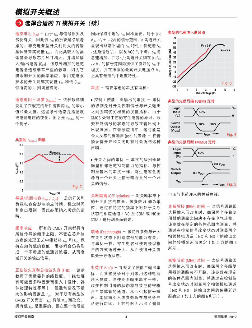
ON-State Resistance (rON) — Because rON contributes to signal loss and degradation, low-rON tradeoffs must be considered. Non-charge pump switches achieve low rON with large pass transistors. These larger tran-sistors lead to larger die sizes and increased CI/O. This additional channel capacitance can be very significant,
of the switch. Switches using charge-pump technology can achieve low rON and CI/O -cantly higher I .
ON-State Resistance Flatness (rON(flat)) — Specifies the minimum and maxi-mum value of rON over the specified range of conditions. These conditions are typically changes in temperature or supply voltage. Figure 2 is an example of rON(flat).
Typical rON(flat) Measurement
On/Off Capacitance (CON/COFF) — Total switch and load capacitance must be considered because it can affect response time, settling time and fanout limits.
— All CMOS switches have an upper limit to the
matter how low rON and CI/O can be maintained in the chip manufacturing process, they still form an undesired low-pass filter that attenuates the switch output signal.
Sine-Wave Distortion or Total Harmonic Distortion (THD) — These are measure-ments of the linearity of the device. Nonlinearity can be introduced in a number of ways (design, device physics, etc.); but typically the largest contributor is rON, which varies with VI/O for all types of CMOS switches. Having a low rON is important, but
a flat rON over the signal range is as
0 < VI/O < (V – 2 V), n-channel switch-es exhibit very flat rON characteristics; but rON increases very rapidly as VI/O approaches V and VGS decreases. Parallel n-/p-channel switches offer good rON flatness for signal ranges of 0 < VI/O < V , with the best flatness characteristic at the highest recom-mended switch V .
Crosstalk — There are two types of crosstalk to consider:
level of crosstalk is a mea sure of how well decoupled the switch control signal is from the switch output. Due to the parasitic capacitance of CMOS processes, changing the state on the control signal causes noise to appear on the output. In audio applications, this can be a source of the annoying pop that is sometimes heard when switching the unit on or off.
of crosstalk also is a measure of adjacent-channel rejection. As with control-to-output crosstalk, parasitic capacitance can couple the signal on one switch with that on another switch.
OFF Isolation — A measurement of OFF-state switch impedance. It is
with the corresponding channel (NC to COM or NO to COM) in the OFF state.
Feedthrough — This characteristic is related to the ability of the switch to block signals when off. As with crosstalk, parasitic capacitance allows
switch, making it appear to be on.
Charge Injection (Q) — TI specifies enable-to-output crosstalk, and some competitors use this parameter. As with enable-to-output crosstalk, changing the state on the control pin causes a charge to be coupled to the channel of the transistor, introducing signal noise. It is presented in this report for a relative comparison with the competition. A graph of bias voltage vs. charge injection is displayed in figure 3 above.
Typical Charge Injection Plot
Typical BBM Timing
Typical MMB Timing
tBBM
50%
90% 90%
LogicInput
(VI)
SwitchOutput(VCOM)
V+
0
50%LogicInput
(VI)
V+
0
tMBB
0.8 VOUT
0.8 V
VNC
SwitchOutput
VNO
OUT
-30-20-10
010203040506070
0 1 2 3 4 5 6Bias Voltage (V)
Cha
rge
Inje
ctio
n (p
C)
V+ = 3 VV+ = 5 V
V (V)COM
r(
)on
(flat
)Ω
2.5
2.0
1.5
1.0
0.5
0
Flatness
Break-Before-Make (BBM) Time — Guarantees that two multiplexer paths are never electrically connected when the signal path is changed by the select input. This parameter is measured under a specified range of conditions and by the propagation delay between the output of two ad-jacent analog channels (NC and NO), when the control signal changes state (as shown in figure 4 above).
Make-Before-Break (MBB) Time — Guarantees that two multiplexer paths are never open when the signal path is changed by the select input. This parameter is measured under a specified range of conditions and by the propagation delay between the output of two adjacent analog channels (NC and NO), when the control signal changes state (as shown in figure 5 above).
Fig. 2
Fig. 3
Fig. 4
Fig. 5
模拟开关指南 4 德州仪器 2012
模拟开关概述
选择合适的 TI 模拟开关(续)
通态电阻 (rON) - 由于 rON 与信号损失及劣化有关,因此低 rON 的折衷是必须考虑的。非充电泵型开关利用大的传输晶体管来实现低 rON。而此类较大的晶体管会导致芯片尺寸增大,并增加输入/输出电容 (CI/O)。该额外增加的通道电容会造成非常严重的影响,因为它将限制开关的频率响应。采用充电泵技术的开关能够实现低 rON 和低 CI/O,但所需的 I+ 则明显提高。
通态电阻平坦度 (rON(flat)) - 该参数详细说明了在规定的条件范围内 rON 的最小值和最大值。这些条件通常是指温度或电源电压的变化。图 2 是 rON(flat) 的一个例子。
导通/关断电容 (CON / COFF) - 总的开关和负载电容会影响响应时间、稳定时间和扇出限制,因此必须纳入考虑的范畴。
频率响应 - 所有的 CMOS 开关都具有所能传导的频率上限。不管在芯片制造商的处理工艺中能够将 rON 和 CI/O 保持在如何低的数值,阻容耦合仍将形成一个不希望的低通滤波器,从而衰减开关的输出信号。
正弦波失真和总谐波失真 (THD) - 该参数用于衡量器件的线性度。非线性度有可能因多种因素而引入(设计、器件物理特性等等);但通常情况下最大的影响因素是 rON,对于所有类型的 CMOS 开关而言,rON 将随 VI/O 而改变。拥有低 rON 是重要的,但在整个信号范
典型的 rON(flat) 测量
典型的电荷注入曲线图
典型的先断后接 (BBM) 定时
典型的先接后断 (MMB) 定时
围内保持平坦的 rON 同样重要。对于 0 < VI/O < (V+ – 2V) 的信号范围,n 沟道开关呈现出非常平坦的 rON 特性;但随着 VI/
O 逐渐逼近 V+、以及 VGS 的下降,rON 将急速增加。并联n / p沟道开关则在 0 < VI/
O < V+ 的信号范围内提供了良好的 rON 平坦度,并在推荐的最高开关电压点 V+ 上具有最佳的平坦度特性。
串扰 - 需要考虑的串扰有两种:
控制(使能)至输出的串扰 - 串扰的级别是对开关控制信号与开关输出之间去耦优劣程度的度量指标。由于 CMOS 处理工艺的寄生电容的原因,改变控制信号的状态将导致在输出端上出现噪声。在音频应用中,这可能是令人反感的劈啪声 (pop) 的来源 - 在音频设备开启和关闭时有时会听到这种声响。
开关之间的串扰 - 串扰的级别也是衡量相邻通道抑制能力的指标。与控制至输出的串扰一样,寄生电容会将源自一个开关上信号耦合至另一个开关的信号。
关断隔离 (OFF Isolation) - 对关断状态下的开关阻抗的度量。该参数以 dB为单位,通过在特定的频率下对处于关断状态的相应通道(NC 至 COM 或 NO至 COM)进行测量而确定。
馈通 (Feedthrough) - 该特性参数与开关在关断状态下阻隔信号的能力有关。与串扰一样,寄生电容可使高频以耦合的方式通过开关,从而使得开关看似处于导通状态。
电荷注入 (Q) - TI 规定了使能至输出串扰,而某些竞争对手则采用这种电荷注入参数。与使能至输出串扰一样,改变控制引脚的状态将导致电荷被耦合至晶体管的通道,从而引起信号噪声。本指南引入该参数旨在与竞争产品进行对比。上方的图 3 示出了偏置
电压与电荷注入的关系曲线。
先断后接 (BBM) 时间 - 当信号通路因选择输入而改变时,确保两个多路复用器的通路之间决不存在电气连接。该参数在规定的条件范围内测量,并通过在控制信号改变状态时测量两个相邻模拟通道(NC 和 NO)的输出之间的传播延迟而确定(如上方的图 4 所示)。
先接后断 (MBB) 时间 - 当信号通路因选择输入而改变时,确保两个多路复用器的通路决不开路。该参数在规定的条件范围内测量,并通过在控制信号改变状态时测量两个相邻模拟通道(NC 和 NO)的输出之间的传播延迟而确定(如上方的图 5 所示)。
模拟开关指南 5 德州仪器 20125Analog Switch Guide Texas Instruments 2012
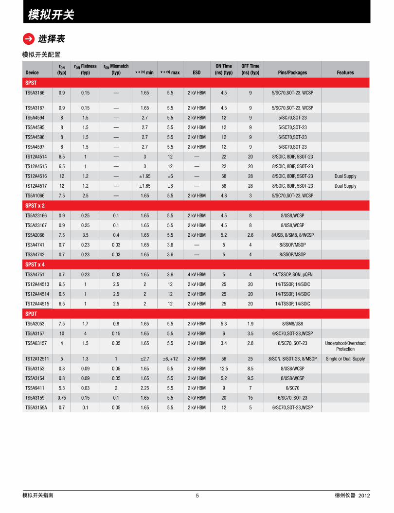
Analog Switches
Selection Tables
DevicerON
(typ)rON Flatness
(typ)rON Mismatch
(typ) v + (v) min v + (v) max ESDON Time(ns) (typ)
OFF Time(ns) (typ) Pins/Packages Features
SPST
TS5A3166 0.9 0.15 — 1.65 5.5 2 kV HBM 4.5 9 5/SC70,SOT-23, WCSP
TS5A3167 0.9 0.15 — 1.65 5.5 2 kV HBM 4.5 9 5/SC70,SOT-23, WCSP
TS5A4594 8 1.5 — 2.7 5.5 2 kV HBM 12 9 5/SC70,SOT-23
TS5A4595 8 1.5 — 2.7 5.5 2 kV HBM 12 9 5/SC70,SOT-23
TS5A4596 8 1.5 — 2.7 5.5 2 kV HBM 12 9 5/SC70,SOT-23
TS5A4597 8 1.5 — 2.7 5.5 2 kV HBM 12 9 5/SC70,SOT-23
TS12A4514 6.5 1 — 3 12 — 22 20 8/SOIC, 8DIP, 5SOT-23
TS12A4515 6.5 1 — 3 12 — 22 20 8/SOIC, 8DIP, 5SOT-23
TS12A4516 12 1.2 — ±1.65 ±6 — 58 28 8/SOIC, 8DIP, 5SOT-23 Dual Supply
TS12A4517 12 1.2 — ±1.65 ±6 — 58 28 8/SOIC, 8DIP, 5SOT-23 Dual Supply
TS5A1066 7.5 2.5 — 1.65 5.5 2 kV HBM 4.8 3 5/SC70,SOT-23, WCSP
SPST x 2
TS5A23166 0.9 0.25 0.1 1.65 5.5 2 kV HBM 4.5 8 8/US8,WCSP
TS5A23167 0.9 0.25 0.1 1.65 5.5 2 kV HBM 4.5 8 8/US8,WCSP
TS5A2066 7.5 3.5 0.4 1.65 5.5 2 kV HBM 5.2 2.6 8/USB, 8/SM8, 8/WCSP
TS3A4741 0.7 0.23 0.03 1.65 3.6 — 5 4 8/SSOP/MSOP
TS3A4742 0.7 0.23 0.03 1.65 3.6 — 5 4 8/SSOP/MSOP
SPST x 4
TS3A4751 0.7 0.23 0.03 1.65 3.6 4 kV HBM 5 4 14/TSSOP, SON, µQFN
TS12A44513 6.5 1 2.5 2 12 2 kV HBM 25 20 14/TSSOP, 14/SOIC
TS12A44514 6.5 1 2.5 2 12 2 kV HBM 25 20 14/TSSOP, 14/SOIC
TS12A44515 6.5 1 2.5 2 12 2 kV HBM 25 20 14/TSSOP, 14/SOIC
SPDT
TS5A2053 7.5 1.7 0.8 1.65 5.5 2 kV HBM 5.3 1.9 8/SM8/US8
TS5A3157 10 4 0.15 1.65 5.5 2 kV HBM 6 3.5 6/SC70,SOT-23,WCSP
TS5A63157 4 1.5 0.05 1.65 5.5 2 kV HBM 3.4 2.8 6/SC70, SOT-23 Undershoot/Overshoot Protection
TS12A12511 5 1.3 1 ±2.7 ±6, +12 2 kV HBM 56 25 8/SON, 8/SOT-23, 8/MSOP Single or Dual Supply
TS5A3153 0.8 0.09 0.05 1.65 5.5 2 kV HBM 12.5 8.5 8/US8/WCSP
TS5A3154 0.8 0.09 0.05 1.65 5.5 2 kV HBM 5.2 9.5 8/US8/WCSP
TS5A9411 5.3 0.03 2 2.25 5.5 2 kV HBM 9 7 6/SC70
TS5A3159 0.75 0.15 0.1 1.65 5.5 2 kV HBM 20 15 6/SC70, SOT-23
TS5A3159A 0.7 0.1 0.05 1.65 5.5 2 kV HBM 12 5 6/SC70,SOT-23,WCSP
Fig. 3
Fig. 4
Fig. 5
Analog Switch Configurations
模拟开关
选择表
模拟开关配置
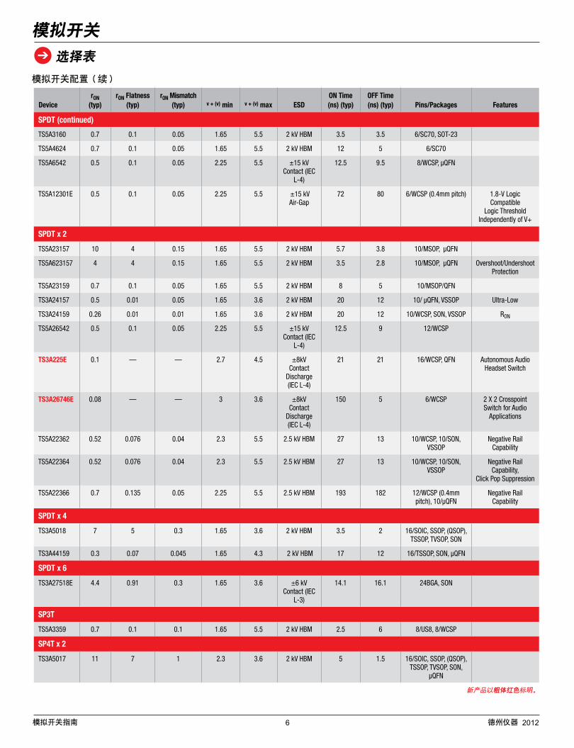
模拟开关指南 6 德州仪器 20126Analog Switch Guide Texas Instruments 2012
DevicerON
(typ)rON Flatness
(typ)rON Mismatch
(typ) v + (v) min v + (v) max ESDON Time(ns) (typ)
OFF Time(ns) (typ) Pins/Packages Features
SPDT (continued)
TS5A3160 0.7 0.1 0.05 1.65 5.5 2 kV HBM 3.5 3.5 6/SC70, SOT-23
TS5A4624 0.7 0.1 0.05 1.65 5.5 2 kV HBM 12 5 6/SC70
TS5A6542 0.5 0.1 0.05 2.25 5.5 ±15 kV Contact (IEC
L-4)
12.5 9.5 8/WCSP, µQFN
TS5A12301E 0.5 0.1 0.05 2.25 5.5 ±15 kV Air-Gap
72 80 6/WCSP (0.4mm pitch) 1.8-V Logic Compatible
Logic Threshold Independently of V+
SPDT x 2
TS5A23157 10 4 0.15 1.65 5.5 2 kV HBM 5.7 3.8 10/MSOP, µQFN
TS5A623157 4 4 0.15 1.65 5.5 2 kV HBM 3.5 2.8 10/MSOP, µQFN Overshoot/Undershoot Protection
TS5A23159 0.7 0.1 0.05 1.65 5.5 2 kV HBM 8 5 10/MSOP/QFN
TS3A24157 0.5 0.01 0.05 1.65 3.6 2 kV HBM 20 12 10/ µQFN, VSSOP Ultra-Low
TS3A24159 0.26 0.01 0.01 1.65 3.6 2 kV HBM 20 12 10/WCSP, SON, VSSOP RON
TS5A26542 0.5 0.1 0.05 2.25 5.5 ±15 kV Contact (IEC
L-4)
12.5 9 12/WCSP
TS3A225E 0.1 — — 2.7 4.5 ±8kV Contact
Discharge (IEC L-4)
21 21 16/WCSP, QFN Autonomous Audio Headset Switch
TS3A26746E 0.08 — — 3 3.6 ±8kV Contact
Discharge (IEC L-4)
150 5 6/WCSP 2 X 2 Crosspoint Switch for Audio
Applications
TS5A22362 0.52 0.076 0.04 2.3 5.5 2.5 kV HBM 27 13 10/WCSP, 10/SON, VSSOP
Negative Rail Capability
TS5A22364 0.52 0.076 0.04 2.3 5.5 2.5 kV HBM 27 13 10/WCSP, 10/SON, VSSOP
Negative Rail Capability,
Click Pop Suppression
TS5A22366 0.7 0.135 0.05 2.25 5.5 2.5 kV HBM 193 182 12/WCSP (0.4mm pitch), 10/µQFN
Negative Rail Capability
SPDT x 4
TS3A5018 7 5 0.3 1.65 3.6 2 kV HBM 3.5 2 16/SOIC, SSOP, (QSOP), TSSOP, TVSOP, SON
TS3A44159 0.3 0.07 0.045 1.65 4.3 2 kV HBM 17 12 16/TSSOP, SON, µQFN
SPDT x 6
TS3A27518E 4.4 0.91 0.3 1.65 3.6 ±6 kV Contact (IEC
L-3)
14.1 16.1 24BGA, SON
SP3T
TS5A3359 0.7 0.1 0.1 1.65 5.5 2 kV HBM 2.5 6 8/US8, 8/WCSP
SP4T x 2
TS3A5017 11 7 1 2.3 3.6 2 kV HBM 5 1.5 16/SOIC, SSOP, (QSOP), TSSOP, TVSOP, SON,
µQFN
Analog Switches
Selection Tables
New products are listed in bold red.
Analog Switch Configurations (Continued)
模拟开关
选择表
模拟开关配置(续)
新产品以粗体红色标明。
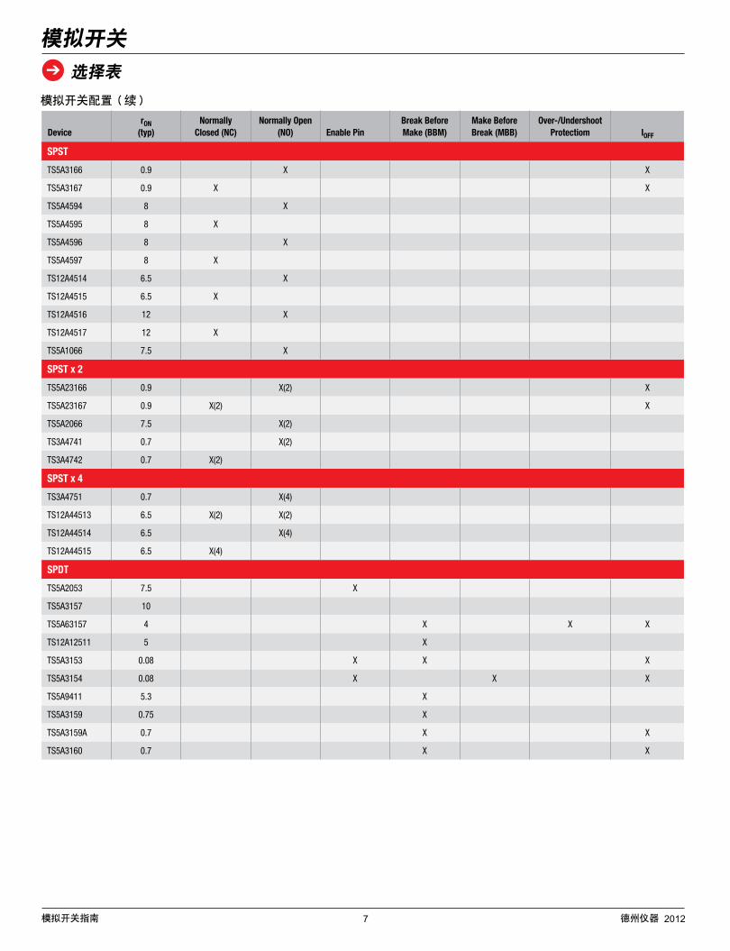
7Analog Switch Guide Texas Instruments 2012
DevicerON
(typ)Normally
Closed (NC)Normally Open
(NO) Enable PinBreak Before Make (BBM)
Make Before Break (MBB)
Over-/Undershoot Protectiom IOFF
SPST
TS5A3166 0.9 X X
TS5A3167 0.9 X X
TS5A4594 8 X
TS5A4595 8 X
TS5A4596 8 X
TS5A4597 8 X
TS12A4514 6.5 X
TS12A4515 6.5 X
TS12A4516 12 X
TS12A4517 12 X
TS5A1066 7.5 X
SPST x 2
TS5A23166 0.9 X(2) X
TS5A23167 0.9 X(2) X
TS5A2066 7.5 X(2)
TS3A4741 0.7 X(2)
TS3A4742 0.7 X(2)
SPST x 4
TS3A4751 0.7 X(4)
TS12A44513 6.5 X(2) X(2)
TS12A44514 6.5 X(4)
TS12A44515 6.5 X(4)
SPDT
TS5A2053 7.5 X
TS5A3157 10
TS5A63157 4 X X X
TS12A12511 5 X
TS5A3153 0.08 X X X
TS5A3154 0.08 X X X
TS5A9411 5.3 X
TS5A3159 0.75 X
TS5A3159A 0.7 X X
TS5A3160 0.7 X X
Analog Switches
Selection Tables
Analog Switch Configurations (Continued)
模拟开关指南 7 德州仪器 2012
模拟开关
选择表
模拟开关配置(续)
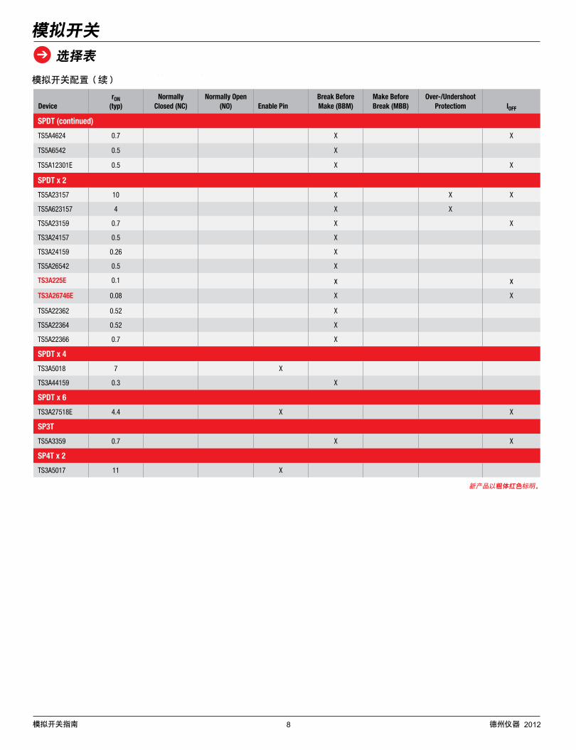
8Analog Switch Guide Texas Instruments 2012
DevicerON
(typ)Normally
Closed (NC)Normally Open
(NO) Enable PinBreak Before Make (BBM)
Make Before Break (MBB)
Over-/Undershoot Protectiom IOFF
SPDT (continued)
TS5A4624 0.7 X X
TS5A6542 0.5 X
TS5A12301E 0.5 X X
SPDT x 2
TS5A23157 10 X X X
TS5A623157 4 X X
TS5A23159 0.7 X X
TS3A24157 0.5 X
TS3A24159 0.26 X
TS5A26542 0.5 X
TS3A225E 0.1 x x
TS3A26746E 0.08 X X
TS5A22362 0.52 X
TS5A22364 0.52 X
TS5A22366 0.7 X
SPDT x 4
TS3A5018 7 X
TS3A44159 0.3 X
SPDT x 6
TS3A27518E 4.4 X X
SP3T
TS5A3359 0.7 X X
SP4T x 2
TS3A5017 11 X
New products are listed in bold red.
Analog Switch Configurations (Continued)
Analog Switches
Selection Tables
模拟开关指南 8 德州仪器 2012
模拟开关
选择表
模拟开关配置(续)
新产品以粗体红色标明。
9Analog Switch Guide Texas Instruments 2012
Analog Switches
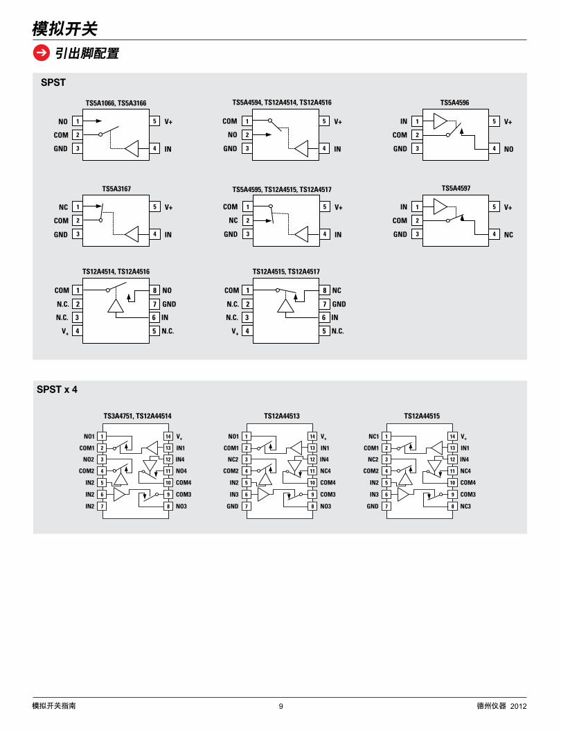
Pinouts
SPST
COM
GND IN
V+NO 1
2
3 4
5
COM
GND IN
V+NC 1
2
3 4
5
TS5A1066, TS5A3166
TS5A3167
TS5A4596
TS5A4597
COM
GND IN
V+
NO
1
2
3 4
5
COM
GND IN
V+
NC
1
2
3 4
5
COM
GND NO
V+IN 1
2
3 4
5
COM
GND NC
V+IN 1
2
3 4
5
TS5A4594, TS12A4514, TS12A4516
TS5A4595, TS12A4515, TS12A4517
TS12A4514, TS12A4516
N.C.
N.C.
V+
COM
GND
IN
N.C.
NO
7
6
5
8
2
3
4
1
N.C.
N.C.
V+
COM
GND
IN
N.C.
NC
7
6
5
8
2
3
4
1
TS12A4515, TS12A4517
SPST x 4
COM1
NO2
COM2
IN2
NO1 1
2
3
4
5
IN2 6
IN2 7
IN1
IN4
NO4
COM4
V+14
13
12
11
10
COM39
NO38
TS3A4751, TS12A44514
COM1
NO1
V–
GND
IN1 1
2
3
4
5
NO4 6
COM4 7
COM2
NO2
V+
N.C.
IN216
15
14
13
12
N0311
COM3
IN4 IN3
10
8 9
TS12A44516, TS40A41612, TS40A41642
COM1
NC2
COM2
IN2
NO1 1
2
3
4
5
IN3 6
GND 7
IN1
IN4
NC4
COM4
V+14
13
12
11
10
COM39
NO38
TS12A44513
COM1
NC2
COM2
IN2
NC1 1
2
3
4
5
IN3 6
GND 7
IN1
IN4
NC4
COM4
V+14
13
12
11
10
COM39
NC38
TS12A44515
COM1
NC1
V–
GND
IN1 1
2
3
4
5
NC4 6
COM4 7
COM2
NC2
V+
N.C.
IN216
15
14
13
12
NC311
COM3
IN4 IN3
10
8 9
TS12A44517, TS40A41611, TS40A41641
COM1
NO1
V–
GND
IN1 1
2
3
4
5
NO4 6
COM4 7
COM2
NC2
V+
N.C.
IN216
15
14
13
12
NC311
COM3
IN4 IN3
10
8 9
TS12A44518
模拟开关指南 9 德州仪器 2012
模拟开关
引出脚配置
10Analog Switch Guide Texas Instruments 2012
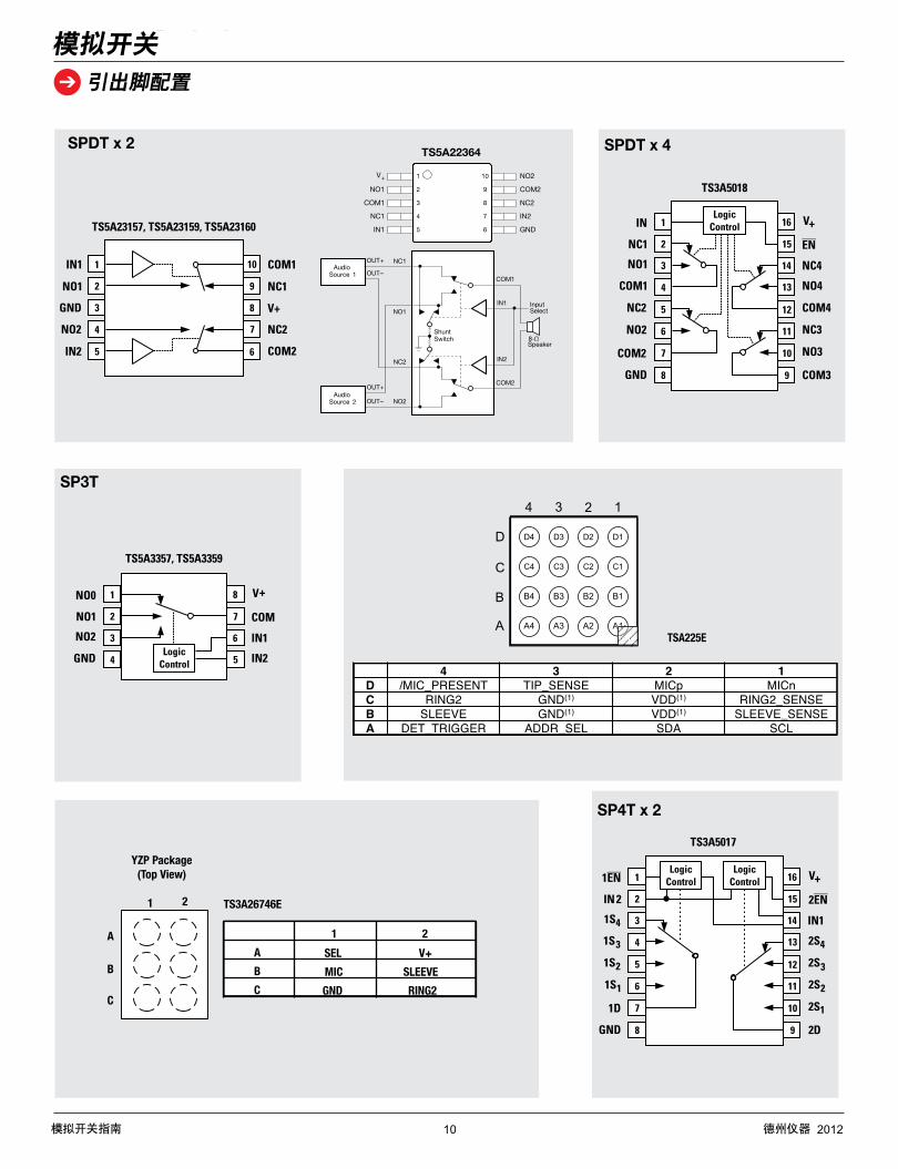
SP3T
SP4T x 2
NO1
NO2
GND
IN1
V+
IN2
NO0
COM
LogicControl
1
2
3
4
8
7
6
5
TS5A3357, TS5A3359
10
11
7
1S2
1
2
3
4
5
16
15
14
13
12
IN 2
1S4
1S3
IN1
V+
2S4
2S3
6
1D
1S1 2S2
2S1
8GND 9 2D
1EN
2EN
LogicControl
LogicControl
TS3A5017
SPDT x 4SPDT x 2
Input Select
ShuntSwitch
IN2
IN1
COM2
COM1
NC2
NC1
NO2
OUT+
OUT+
OUT–
OUT–
NO1
TS5A22364
AudioSource 1
AudioSource 2
8-Speaker
Ω
1
2
3
4
5
10
9
8
7
6
NO2
COM2
NC2
IN2
V+
NO1
COM1
NC1
IN1 GND
NO1
GND
NO2
IN2
IN1 COM1
NC1
NC2
COM2
V+
1
2
3
4
5
10
9
8
7
6
TS5A23157, TS5A23159, TS5A23160
10
11
7
NC2
1
2
3
4
5
16
15
14
13
12
NC1
NO1
COM1
NC4
V+
NO4
COM4
6
COM2
NO2 NC3
NO3
8GND 9 COM3
IN
EN
LogicControl
TS3A5018
Analog Switches
Pinouts
A4
D
C
B
A
4 3 2 1
A3 A2 A1
B4 B3 B2 B1
C4 C3 C2 C1
D4 D3 D2 D1
A1
4 3 2 1D /MIC_PRESENT TIP_SENSE MICp MICnC RING2 GND(1) VDD(1) RING2_SENSEB SLEEVE GND(1) VDD(1) SLEEVE_SENSEA DET_TRIGGER ADDR_SEL SDA SCL
TSA225E
1 2
A
B
C
1 2 A SEL V+ B MIC SLEEVE C GND RING2
TS3A26746E
YZP Package(Top View)
模拟开关指南 10 德州仪器 2012
模拟开关
引出脚配置
11Analog Switch Guide Texas Instruments 2012
2x2 Crosspoint Switch for Audio ApplicationsTS3A26746E
Get samples, data sheets and app reports at: www.ti.com/sc/device/ts3a26746e
Key Features
(-75 dB)
compatible
o ±8-kV contact discharge (IEC 61000-4-2)
package (1.45 x 0.95 x 0.5 mm)
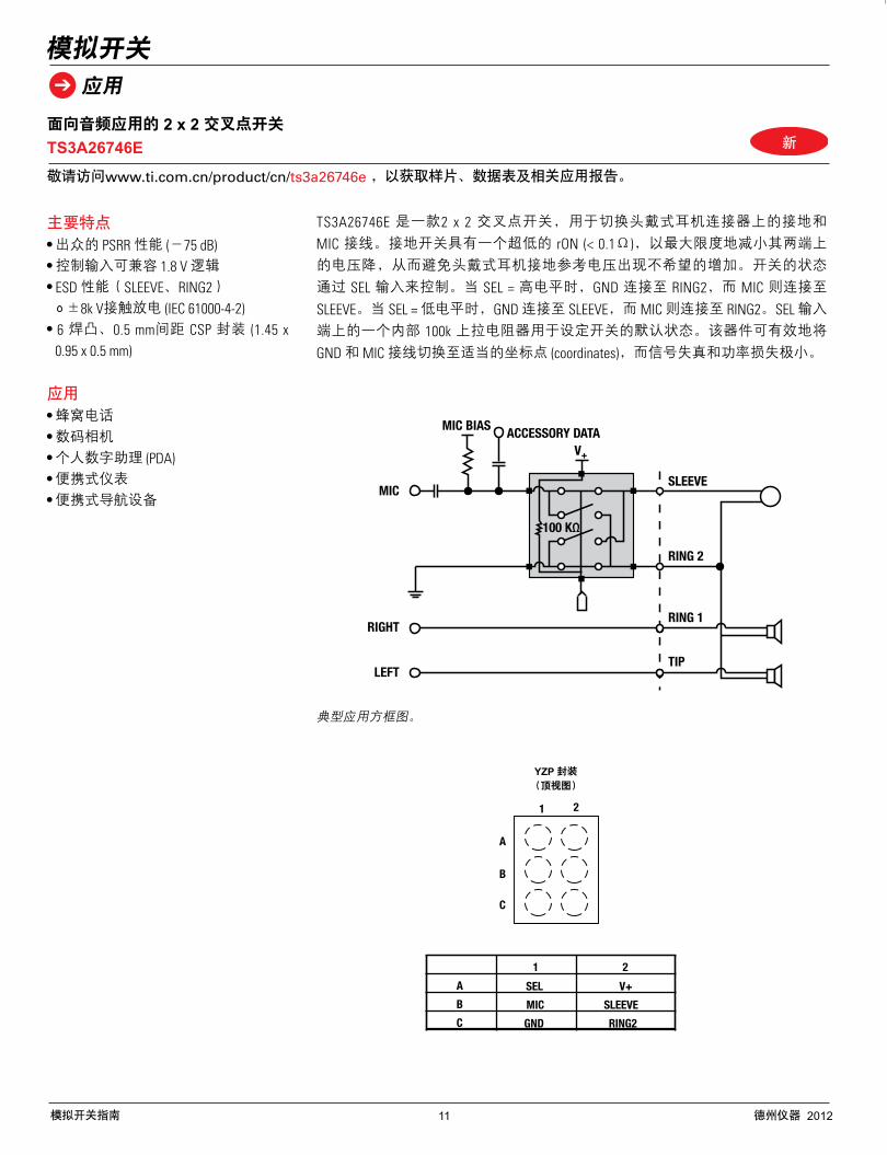
Applications
The TS3A26746E is a 2 × 2 cross-point switch that is used to interchange the ground and MIC connections on a headphone connector. The ground switch has an ultra low rON of <0.1 Ω to minimize voltage drop across it, preventingundesired increases in headphone ground reference voltage. The switch state is controlled via the SEL input. When SEL=High, GND is connected to RING2 and MIC is connected to SLEEVE. When SEL=Low, GND is connected to SLEEVE and MIC is connected to RING2. An internal 100k pull-up resistor on the SEL input sets the default state of the switch. This device effectively switches the GND and MIC lines to the appropriate coordinates with minimal signal distortion and power loss.
Analog Switches
Applications
Typical application block diagram.
V+
MIC
RIGHT
LEFTTIP
RING 1
RING 2
100 KΩ
SLEEVE
ACCESSORY DATAMIC BIAS
1 2
A
B
C
1 2 A SEL V+ B MIC SLEEVE C GND RING2
YZP Package(Top View)
面向音频应用的 2 x 2 交叉点开关
TS3A26746E
YZP 封装
(顶视图)
模拟开关指南 11 德州仪器 2012
模拟开关
应用
主要特点 出众的 PSRR 性能 (-75 dB) 控制输入可兼容 1.8 V 逻辑
ESD 性能(SLEEVE、RING2)
±8k V接触放电 (IEC 61000-4-2) 6 焊凸、0.5 mm间距 CSP 封装 (1.45 x 0.95 x 0.5 mm)
应用 蜂窝电话
数码相机
个人数字助理 (PDA) 便携式仪表
便携式导航设备
TS3A26746E 是一款2 x 2 交叉点开关,用于切换头戴式耳机连接器上的接地和 MIC 接线。接地开关具有一个超低的 rON (< 0.1Ω),以最大限度地减小其两端上
的电压降,从而避免头戴式耳机接地参考电压出现不希望的增加。开关的状态
通过 SEL 输入来控制。当 SEL = 高电平时,GND 连接至 RING2,而 MIC 则连接至 SLEEVE。当 SEL = 低电平时,GND 连接至 SLEEVE,而 MIC 则连接至 RING2。SEL 输入
端上的一个内部 100k 上拉电阻器用于设定开关的默认状态。该器件可有效地将 GND 和 MIC 接线切换至适当的坐标点 (coordinates),而信号失真和功率损失极小。
新
敬请访问www.ti.com.cn/product/cn/ts3a26746e ,以获取样片、数据表及相关应用报告。
典型应用方框图。
12Analog Switch Guide Texas Instruments 2012
Analog Switches
Applications
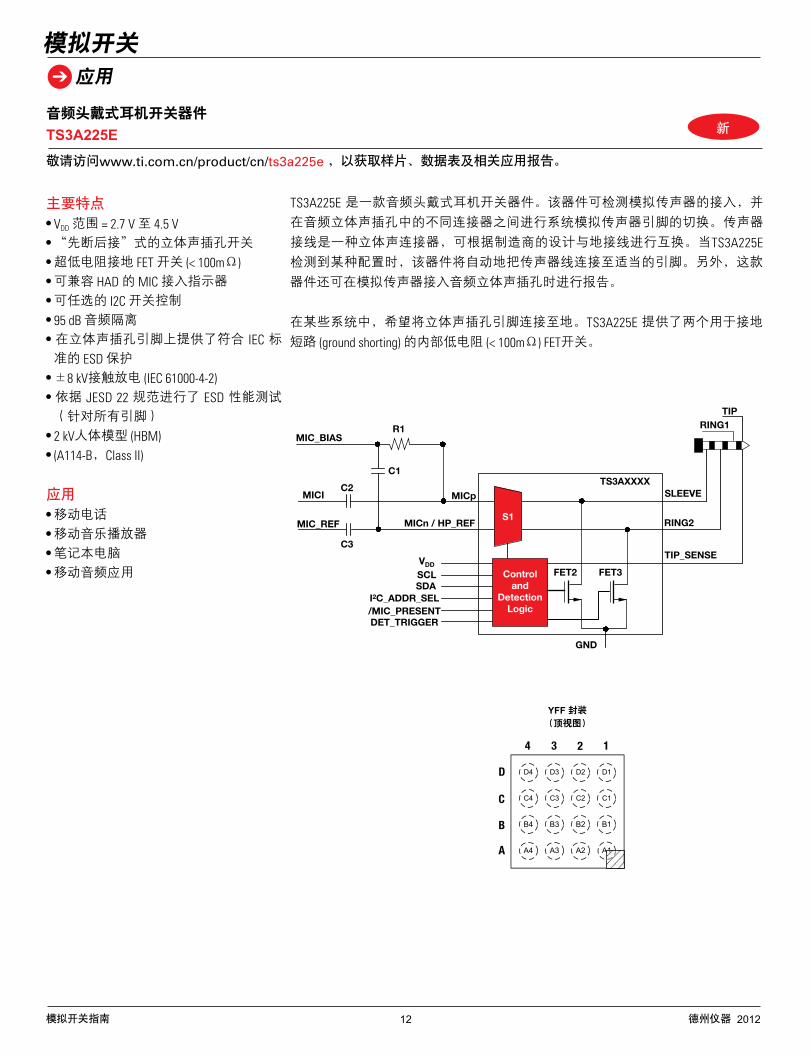
Control and
DetectionLogic
S1
SLEEVETS3AXXXX
TIP
VDD
SCL FET2 FET3
GND
MICp
SDAI2C_ADDR_SEL/MIC_PRESENT
MIC_REF MICn / HP_REF
MIC_BIASR1
C1
C2
C3
MICI
DET_TRIGGER
RING1
RING2
TIP_SENSE
Audio Headset Switch DeviceTS3A225E
Get samples, data sheets and app reports at: www.ti.com/sc/device/ts3a225e
Key Features
DD range = 2.7 V to 4.5 V
switches (< 100 mΩ)
indicator2C switch control
jack pins
22 (all pins)
(A114-B, Class II)
Applications
The TS3A225E is an audio headset switch device. The device detects the pres-ence of an analog microphone and switches a system analog microphone pin between different connectors in an audio stereo jack. The microphone connection in a stereo connector can be swapped with the ground connection depending on manufacturer. When the device detects a certain configuration, it automatically connects the microphone line to the appropriate pin. The device also reports the presence of an analog microphone on an audio stereo jack.
In some systems, it is desirable to connect the stereo jack pin to ground. The TS3A225E provides two internal low resistance (<100 m) FET switches for ground shorting.
A4
D
C
B
A
4 3 2 1
A3 A2 A1
B4 B3 B2 B1
C4 C3 C2 C1
D4 D3 D2 D1
A1
YFF Package(Top View)
模拟开关指南 12 德州仪器 2012
音频头戴式耳机开关器件
TS3A225E
模拟开关
应用
主要特点 VDD 范围 = 2.7 V 至 4.5 V “先断后接”式的立体声插孔开关
超低电阻接地 FET 开关 (< 100mΩ) 可兼容 HAD 的 MIC 接入指示器
可任选的 I2C 开关控制
95 dB 音频隔离
在立体声插孔引脚上提供了符合 IEC 标准的 ESD 保护
±8 kV接触放电 (IEC 61000-4-2) 依据 JESD 22 规范进行了 ESD 性能测试(针对所有引脚)
2 kV人体模型 (HBM) (A114-B,Class II)
应用 移动电话
移动音乐播放器
笔记本电脑
移动音频应用
敬请访问www.ti.com.cn/product/cn/ts3a225e ,以获取样片、数据表及相关应用报告。
新
TS3A225E 是一款音频头戴式耳机开关器件。该器件可检测模拟传声器的接入,并
在音频立体声插孔中的不同连接器之间进行系统模拟传声器引脚的切换。传声器
接线是一种立体声连接器,可根据制造商的设计与地接线进行互换。当TS3A225E 检测到某种配置时,该器件将自动地把传声器线连接至适当的引脚。另外,这款
器件还可在模拟传声器接入音频立体声插孔时进行报告。
在某些系统中,希望将立体声插孔引脚连接至地。TS3A225E 提供了两个用于接地
短路 (ground shorting) 的内部低电阻 (< 100mΩ) FET开关。
YFF 封装
(顶视图)
13Analog Switch Guide Texas Instruments 2012
±6 V, +12 V 5-Ω SPDT Analog SwitchTS12A12511
Get samples, data sheets and app reports at: www.ti.com/sc/device/ts12a12511
Key Features
operation
operation
with ±5 V supply
±1 nA at 25°C, ±50 nA at 85°C
ON=115 ns, tOFF=56 ns (±5 V supply)
control inputs
QFN packages
Applications
The TS12A12511 is a single-pole double-throw (SPDT) analog switch capable of
well in both directions when it is on. It also offers a low ON-state resistance of 5 (typical), which is matched to within one between channels. The max current consumption is <1 µA and –3 dB bandwidth is >93 MHz. The TS12A12511 exhibits break-before-make switching action, preventing momentary shorting when switching channels. This device is available packaged in an 8-lead MSOP, 8-lead SOT-23, and 8-pin QFN.
TS12A12511 variable gain.
+
-VIN
VOUT
R1=10k
Rf1=20k
Rf2=10k
TS12A125
Variable Gain
+5V
8
7
6
5
COM
NC
GND
V+
NO
V–
IN
N. C.
1
2
3
4
TS12A12511
Analog Switches
Applications
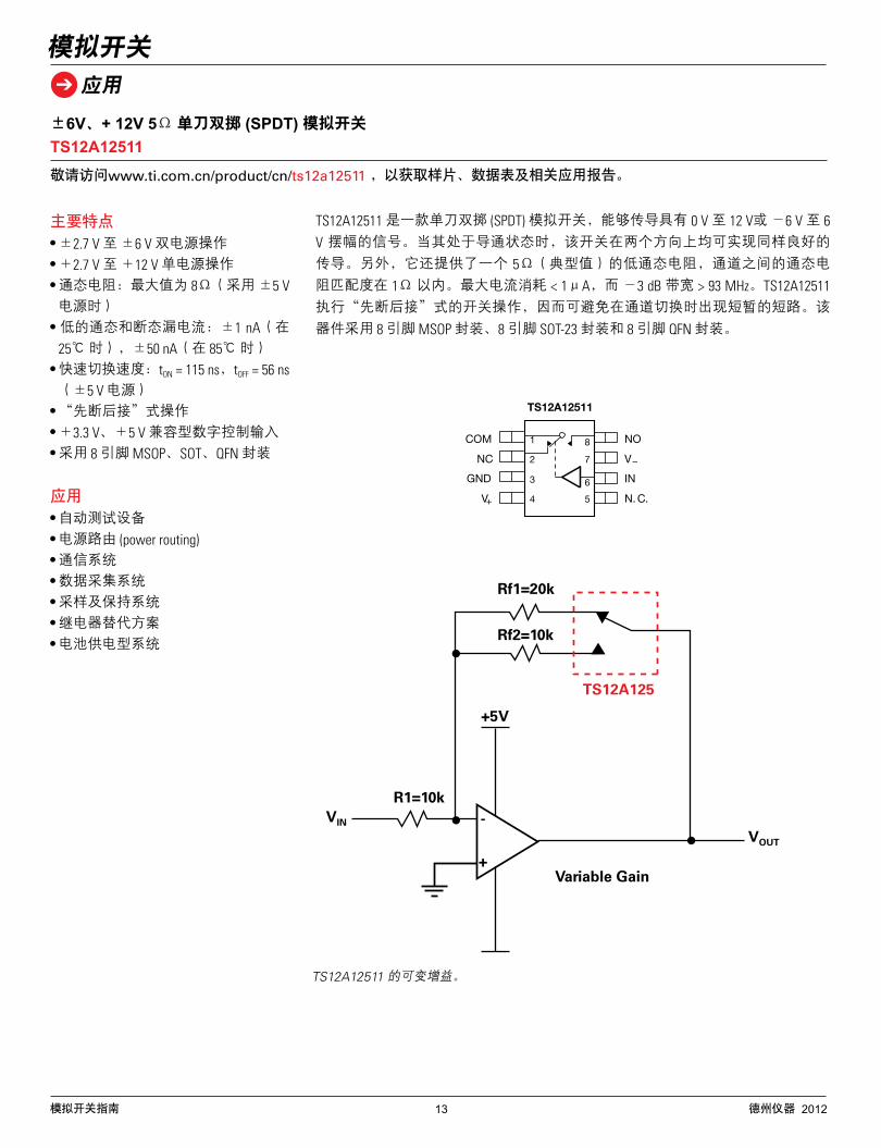
模拟开关指南 13 德州仪器 2012
±6V、+ 12V 5Ω 单刀双掷 (SPDT) 模拟开关
TS12A12511
模拟开关
应用
主要特点 ±2.7 V 至 ±6 V 双电源操作
+2.7 V 至 +12 V 单电源操作
通态电阻:最大值为 8Ω(采用 ±5 V 电源时)
低的通态和断态漏电流:±1 nA(在 25 时),±50 nA(在 85 时)
快速切换速度:tON = 115 ns,tOFF = 56 ns(±5 V 电源)
“先断后接”式操作
+3.3 V、+5 V 兼容型数字控制输入
采用 8 引脚 MSOP、SOT、QFN 封装
应用 自动测试设备
电源路由 (power routing) 通信系统
数据采集系统
采样及保持系统
继电器替代方案
电池供电型系统
敬请访问www.ti.com.cn/product/cn/ts12a12511 ,以获取样片、数据表及相关应用报告。
TS12A12511 是一款单刀双掷 (SPDT) 模拟开关,能够传导具有 0 V 至 12 V或 -6 V 至 6 V 摆幅的信号。当其处于导通状态时,该开关在两个方向上均可实现同样良好的
传导。另外,它还提供了一个 5Ω(典型值)的低通态电阻,通道之间的通态电
阻匹配度在 1Ω 以内。最大电流消耗 < 1μA,而 -3 dB 带宽 > 93 MHz。TS12A12511 执行“先断后接”式的开关操作,因而可避免在通道切换时出现短暂的短路。该
器件采用 8 引脚 MSOP 封装、8 引脚 SOT-23 封装和 8 引脚 QFN 封装。
TS12A12511 的可变增益。
14Analog Switch Guide Texas Instruments 2012
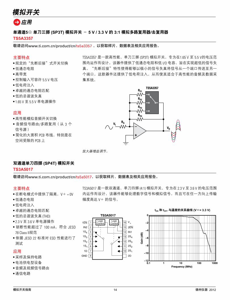
Single 5-Ω SP3T Analog Switch—5-V/3.3-V 3:1 Analog Multiplexer/DemultiplexerTS5A3357
Get samples, data sheets and app reports at: www.ti.com/sc/device/ts5a3357
Key Features
switching
matching
operation
Applications
switching
from three sources
especially on space-constrained PCBs
The TS5A3357 is a high-performance, single-pole, triple-throw (SP3T) analog switch designed to operate from 1.65 V to 5.5 V. It offers low ON-state resistance and low I/O capacitance for very low signal distortion. The break-before-make feature allows transfer of a signal from one port to another with minimal signal distortion. This device also offers a low charge injection, which makes it suitable
Amplifier gain adjustment.
VIVO
TS5A3357
RG
RF4
RF3
RF2
RF1
+
–
Analog Switches
Applications
Dual SP4T Analog SwitchTS3A5017
Get samples, data sheets and app reports at: www.ti.com/sc/device/ts3a5017
Key Features
matching
operation
Applications
designed to operate from 2.3 V to 3.6 V. This device can handle both digital and
1Logic
ControlLogic
Control 16
2 15
3 14
4 13
5 12
6 11
7 10
1EN
IN2
1S4
1S3
1S2
1S1
1D
GND
V+
2EN
IN1
2S4
2S3
2S2
2S1
2D8
TS5A22364
TS3A5017
tON and tOFF vs. Temperature (V+ = 3.3 V)
模拟开关指南 14 德州仪器 2012
单通道5Ω 单刀三掷 (SP3T) 模拟开关 - 5 V / 3.3 V 的 3:1 模拟多路复用器/去复用器
TS5A3357
模拟开关
应用
主要特点 规定的“先断后接”式开关切换
低通态电阻
高带宽
控制输入可容许 5.5 V 电压
低电荷注入
卓越的通态电阻匹配
低的总谐波失真
1.65 V 至 5.5 V 单电源操作
应用 高性能模拟音频开关切换
音频信号路由/多路复用(从 3 个信号源)
简化的大面积 PCB 布线,特别是在空间受限的 PCB 上
敬请访问www.ti.com.cn/product/cn/ts5a3357 ,以获取样片、数据表及相关应用报告。
TS5A3357 是一款高性能、单刀三掷 (SP3T) 模拟开关,专为在1.65 V 至 5.5 V的电压范
围内运作而设计。该器件提供了低通态电阻和低 I/O 电容,旨在实现超低的信号失
真。“先断后接”特性使得能够以极小的信号失真将信号从一个端口传送至另一
个端口。这款器件还提供了低电荷注入,从而使其适合于高性能的音频及数据采
集系统。
TS3A5017 是一款双通道、单刀四掷 (4:1) 模拟开关,专为在 2.3 V 至 3.6 V 的电压范围
内运作而设计。该器件能够处理数字信号和模拟信号,而且可在任一方向上传输
幅度高达 V+ 的信号。
放大器增益调节。
tON 和 tOFF 与温度的关系曲线 (V+= 3.3 V)
双通道单刀四掷 (SP4T) 模拟开关
TS3A5017敬请访问www.ti.com.cn/product/cn/ts5a5017,以获取样片、数据表及相关应用报告。
主要特点 在断电模式中提供了隔离,V+ = 0V 低通态电阻
低电荷注入
卓越的通态电阻匹配
低的总谐波失真 (THD) 2.3 V 至 3.6 V 单电源操作
锁断性能超过了 100 mA,符合 JESD 78 Class II规范
依据 JESD 22 标准对 ESD 性能进行了测试
应用 采样及保持电路
电池供电型设备
音频及视频信号路由
通信电路
15Analog Switch Guide Texas Instruments 2012
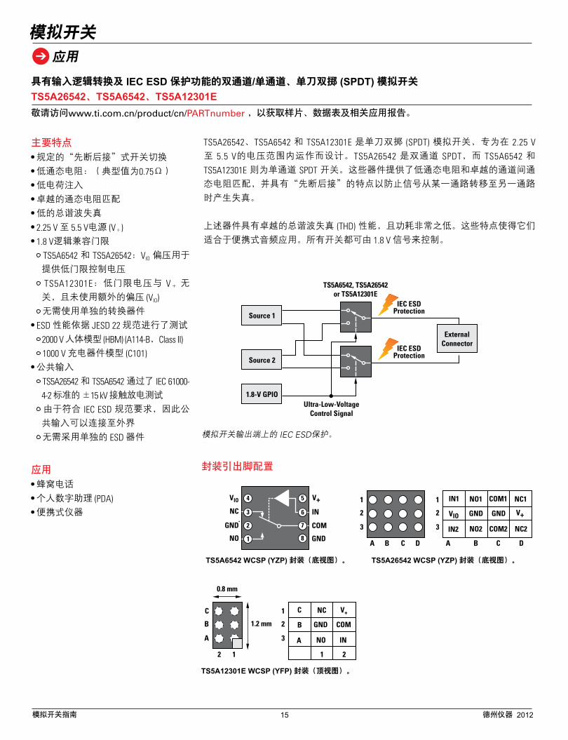
The TS5A26542, TS5A6542, and TS5A12301E are single-pole double-throw (SPDT) analog switches that are designed to operate from 2.25 V to 5.5 V. The TS5A26524 is a dual SPDT, whereas the TS5A6542 and TS5A12301E are single SPDT switches. The devices offer a low ON-state resistance with an excellent channel-to-channel ON-state resistance matching, and the break-before-make feature to prevent signal distortion during the transferring of a signal from one path to another.
These devices have excellent total harmonic distortion (THD) performance and consume very low power. These features make them suitable for portable audio applications. All of the switches can be controlled by 1.8-V signals.
Dual/Single SPDT Analog Switches with Input Logic Translation and IEC ESDTS5A26542, TS5A6542, TS5A12301E
Get samples, data sheets and app reports at: www.ti.com/sc/device/PARTnumber
Key Features
switching
(0.75 Ω typ)
matching
)
TS5A6542 and TS5A26542: VIO bias used to allow low threshold control voltage
TS5A12301E: Low threshold voltage independent of V and no use of additional bias (VIO)
No need for separate translation devices
2000-V Human Body Model (HBM) (A114-B, Class II)
1000-V charged-device model (C101)
±15-kV IEC61000-4-2, contact discharge for TS5A26542 and TS5A6542
Comm inputs can be interfaced to the external world due to IEC ESD compliance
No need for separate ESD devices
Applications
Package Pinouts
TS5A6542 WCSP (YZP) package (bottom view).
TS5A12301E WCSP (YFP) package (top view).
TS5A26542 WCSP (YZP) package (bottom view).
IEC ESD protection on analog switch outputs.
ExternalConnector
IEC ESDProtection
IEC ESDProtection
TS5A6542, TS5A26542or TS5A12301E
Ultra-Low-VoltageControl Signal
Source 1
Source 2
1.8-V GPIO
4
1
2
3
8
6
5
7
GND
VIO V+
NC
NO
IN
COMGND 3
2
1
DCBA
3
2
1
DCBA
GNDGND
COM1
V+VIO
IN1
IN2 COM2
NC1NO1
NO2 NC2
3
2
1
21
A
B
C
12
0.8 mm
1.2 mm COMGND
V+
B
C
A IN
NC
NO
Analog Switches
Applications
模拟开关指南 15 德州仪器 2012
具有输入逻辑转换及 IEC ESD 保护功能的双通道/单通道、单刀双掷 (SPDT) 模拟开关
TS5A26542、TS5A6542、TS5A12301E
模拟开关
应用
主要特点
规定的“先断后接”式开关切换
低通态电阻:(典型值为0.75Ω)
低电荷注入
卓越的通态电阻匹配
低的总谐波失真
2.25 V 至 5.5 V电源 (V+) 1.8 V逻辑兼容门限
TS5A6542 和 TS5A26542:VIO 偏压用于
提供低门限控制电压
TS5A12301E:低门限电压与 V+ 无关,且未使用额外的偏压 (VIO) 无需使用单独的转换器件
ESD 性能依据 JESD 22 规范进行了测试
2000 V 人体模型 (HBM) (A114-B,Class II) 1000 V 充电器件模型 (C101)
公共输入
TS5A26542 和 TS5A6542 通过了 IEC 61000-4-2 标准的 ±15 kV 接触放电测试
由于符合 IEC ESD 规范要求,因此公
共输入可以连接至外界
无需采用单独的 ESD 器件
应用
蜂窝电话
个人数字助理 (PDA) 便携式仪器
敬请访问www.ti.com.cn/product/cn/PARTnumber ,以获取样片、数据表及相关应用报告。
TS5A26542、TS5A6542 和 TS5A12301E 是单刀双掷 (SPDT) 模拟开关,专为在 2.25 V 至 5.5 V的电压范围内运作而设计。TS5A26542 是双通道 SPDT,而 TS5A6542 和 TS5A12301E 则为单通道 SPDT 开关。这些器件提供了低通态电阻和卓越的通道间通
态电阻匹配,并具有“先断后接”的特点以防止信号从某一通路转移至另一通路
时产生失真。
上述器件具有卓越的总谐波失真 (THD) 性能,且功耗非常之低。这些特点使得它们
适合于便携式音频应用。所有开关都可由 1.8 V 信号来控制。
模拟开关输出端上的 IEC ESD保护。
封装引出脚配置
TS5A6542 WCSP (YZP) 封装(底视图)。
TS5A12301E WCSP (YFP) 封装(顶视图)。
TS5A26542 WCSP (YZP) 封装(底视图)。
16Analog Switch Guide Texas Instruments 2012
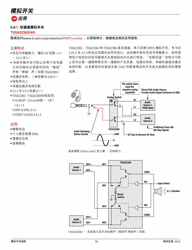
0.6-Ω Dual Analog SwitchesTS5A22362/4/6
Get samples, data sheets and app reports at: www.ti.com/sc/device/PARTnumber
Key Features
Analog I/O range = V –5.5 V to V
audible click-and-pop when switching between two sources (TS5A22364 only)
(0.65-Ω typ)
matching
)
options: 10-WCSP (0.5 mm pitch – YZP)
1.9 x 1.4 SON-10 (DRL) 3 x 3 VSSOP-10 (DGS) 4.9 x 3
Applications
The TS5A22362, TS5A22364, and TS5A22366 are dual single-pole double-throw (SPDT) analog switches that are designed to operate from 2.25 to 5.5 V. The devices feature negative signal capability that allow signals below ground to pass through the switch without distortion. The break-before-make feature prevents signal distortion during the transferring of a signal from one path to another. Low ON-state resistance, excellent channel-to-channel ON-state resistance matching, and minimal total harmonic distortion (THD) performance make these switches ideal for audio applications.
Direct path amplifier – negative rail capability.
TS5A22364 – negative rail capability and click-pop suppression
RefAudio
Source 1TPA6130A2
Direct Path Audio SourceProvide Audio Signal Centered on GND
The switch doesneed the
negative swingcapability
Traditional Class AB(No Neg Signal)
Audio Source 2
R L
R1
L1
R2
L2
DC Cap to Remove DC Bias
Analog Switch
TS5A22362
+VDDAudio SwingingBelow Ground
0
–VDD
Audio Source 2
Audio Source 1
TS5A22364
COM1
NC1
ShuntSwitch
NO1
NC2
NO2
OUT+
OUT–
OUT+
OUT–
IN1
COM2
IN2
Input Select
8-Ω Speaker
Analog Switches
Applications
模拟开关指南 16 德州仪器 2012
0.6Ω 双通道模拟开关
TS5A22362/4/6
模拟开关
应用
主要特点
负信号传输能力:模拟 I/O 范围 = V+ - 5.5 V 至 V+
内部并联开关可防止在两个信号源
之间切换时出现能听到的“喀呖”
声和“劈啪”声(仅限 TS5A22364)
低通态电阻:(典型值为 0.65Ω)
低电荷注入
卓越的通态电阻匹配
2.3 V 至 5.5 V 电源 (V+) TS5A22362 / TS5A22364封装选项:
10-WCSP(0.5 mm间距 - YZP)
1.9 x 1.4 SON-10 (DRL) 3 x 3 VSSOP-10 (DGS) 4.9 x 3
应用
蜂窝电话
个人数字助理 (PDA) 便携式仪表
音频路由
敬请访问www.ti.com.cn/product/cn/PARTnumber ,以获取样片、数据表及相关应用报告。
TS5A22362、TS5A22364 和 TS5A22366 是双通道、单刀双掷 (SPDT) 模拟开关,专为在 2.25 V 至 5.5 V的电压范围内运作而设计。这些器件具有负信号传输能力,因而使
得低于地电位的信号能够无失真地经由开关进行传送。“先断后接”的特点可防
止信号从某一通路转移至另一通路时产生失真。低通态电阻、卓越的通道间通态
电阻匹配、以及极低的总谐波失真 (THD) 性能使得这些开关成为音频应用的理想
选择。
直接通路 (Direct path) 放大器 - 负轨能力。
TS5A22364 - 负轨能力及开关机噪声(喀呖声-劈啪声)抑制。
17Analog Switch Guide Texas Instruments 2012
Device Configuration
VCC (VDD)rON
(typ)( )
Bandwidth(MHz)
Off Isolation
(dB)ICC (IDD)(typ)(µA)
Pins/Packages Description(min) (V)
(max) (V)
Crosstalk(dB)
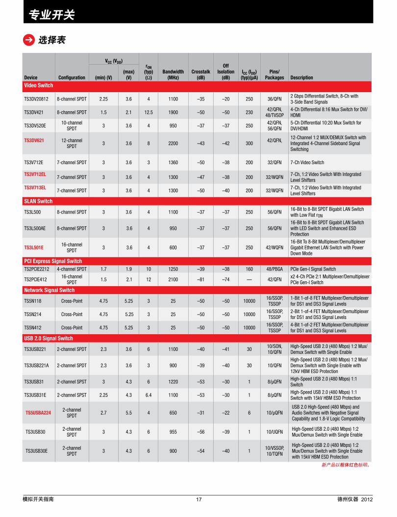
Video Switch
TS3DV20812 8-channel SPDT 2.25 3.6 4 1100 –35 –20 250 36/QFN 2 Gbps Differential Switch, 8-Ch with 3-Side Band Signals
TS3DV421 8-channel SPDT 1.5 2.1 12.5 1900 –50 –50 230 42/QFN, 48/TVSOP
4-Ch Differential 8:16 Mux Switch for DVI/HDMI
TS3DV520E 10-channel SPDT 3 3.6 4 950 –37 –37 250 42/QFN,
56/QFN5-Ch Differential 10:20 Mux Switch for DVI/HDMI
TS3DV621 12-channel SPDT 3 3.6 8 2200 –43 –42 300 42/QFN, 12-Channel 1:2 MUX/DEMUX Switch with
Integrated 4-Channel Sideband Signal Switching
TS3V712E 7-channel SPDT 3 3.6 3 1360 –50 –38 200 32/QFN 7-Ch Video Switch
TS3V712EL 7-channel SPDT 3 3.6 4 1300 –47 –38 200 32/WQFN 7-Ch, 1:2 Video Switch With Integrated Level Shifters
TS3V713EL 7-channel SPDT 3 3.6 4 1300 –50 –40 200 32/WQFN 7-Ch, 1:2 Video Switch With Integrated Level Shifters
SLAN Switch
TS3L500 8-channel SPDT 3 3.6 4 1100 –37 –37 250 56/QFN 16-Bit to 8-Bit SPDT Bigabit LAN Switch with Low Flat rON
TS3L500AE 8-channel SPDT 3 3.6 4 950 –37 –37 250 56/QFN16-Bit to 8-Bit SPDT Gigabit LAN Switch with LED Switch and Enhanced ESD Protection
TS3L501E 16-channel SPDT 3 3.6 4 600 –37 –37 250 42/WQFN
16-Bit To 8-Bit Multiplexer/Demultiplexer Gigabit Ethernet LAN Switch with Power Down Mode
PCI Express Signal SwitchTS2PCIE2212 4-channel SPDT 1.7 1.9 10 1250 –39 –38 160 48/PBGA PCIe Gen-I Signal Switch
TS2PCIE412 16-channel SPDT 1.5 2.1 12 2100 –81 –74 — 42/QFN x2 4-Ch PCIe 2:1 Multiplexer/Demultiplexer
PCIe Gen-I Switch
Network Signal Switch
TS5N118 Cross-Point 4.75 5.25 3 25 –50 –50 10000 16/SSOP, TSSOP
1-Bit 1-of-8 FET Multiplexer/Demultiplexer for DS1 and DS3 Signal Levels
TS5N214 Cross-Point 4.75 5.25 3 25 –50 –50 10000 16/SSOP, TSSOP
2-Bit 1-of-4 FET Multiplexer/Demultiplexer for DS1 and DS3 Signal Levels
TS5N412 Cross-Point 4.75 5.25 3 25 –50 –50 10000 16/SSOP, TSSOP
4-Bit 1-of-2 FET Multiplexer/Demultiplexer for DS1 and DS3 Signal Levels
USB 2.0 Signal Switch
TS3USB221 2-channel SPDT 2.3 3.6 6 1100 –40 –41 30 10/SON,10/QFN
High-Speed USB 2.0 (480 Mbps) 1:2 Mux/Demux Switch with Single Enable
TS3USB221A 2-channel SPDT 2.3 3.6 3 900 –39 –40 30 10/QFNHigh-Speed USB 2.0 (480 Mbps) 1:2 Mux/Demux Switch with Single Enable with 12kV HBM ESD Protection
TS3USB31 2-channel SPST 3 4.3 6 1220 –53 –30 1 8/µQFN High-Speed USB 2.0 (480 Mbps) 1:1 Switch
TS3USB31E 2-channel SPST 2.25 4.3 6.4 1100 –53 –30 1 8/µQFN High-Speed USB 2.0 (480 Mbps) 1:1 Switch with 15kV HBM ESD Protection
TS5USBA224 2-channel SPDT 2.7 5.5 4 650 –31 –22 6 10/µQFN
USB 2.0 High-Speed (480 Mbps) and Audio Switches with Negative Signal Capability and 1.8-V Logic Compatibility
TS3USB30 2-channel SPDT 3 4.3 6 955 –56 –39 1 10/UQFN High-Speed USB 2.0 (480 Mbps) 1:2
Mux/Demux Switch with Single Enable
TS3USB30E 2-channel SPDT 3 4.3 6 900 –54 –40 1 10/VSSOP,
10/TQFN
High-Speed USB 2.0 (480 Mbps) 1:2 Mux/Demux Switch with Single Enable with 15kV HBM ESD Protection
Specialty Switches
Selection Tables
New products are listed in bold red.
模拟开关指南 17 德州仪器 2012
专业开关
选择表
新产品以粗体红色标明。
18Analog Switch Guide Texas Instruments 2012
Specialty Switches
Selection Tables
Device Configuration nCH
Vcc (Vdd)rON
(max) ( )
Bandwidth(MHz)
Off Isolation
(dB)
ICC (IDD)Max (µA)
Pins/
Packages Description(min)
(V)(max)
(V)Crosstalk
(dB)
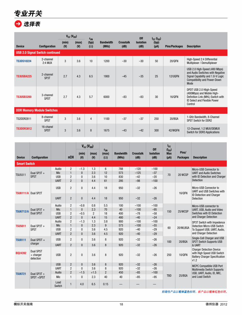
Smart Switch
TSU5511 Dual SP3T + SPST
Audio 2 –1.3 1.3 6 788 –120 –100
70 20 WCSP
Micro-USB Connector to UART and Audio Switches with ID Detection and Charger Detection
Mic 1 0 2.3 12 573 –125 –37USB 2 0 3.6 10 830 –42 –20UART 2 0 4.4 61 295 –98 –100
TSU6111/A Dual SP2T
USB 2 0 4.4 18 950 –32 –26
16/QFN
Micro-USB Connector to UART and USB Switches with ID Detection and Charger DetectionUART 2 0 4.4 18 950 –32 –26
TSU6712/A Dual SP3T + Dual SPST
Audio 2 –0.8 0.8 5.5 100 –100 –100
150 25/WCSP
Micro-USB connector to UART, USB, Audio and Video Switches with ID Detection and Charger Detection
Mic 1 0 2.3 70 40 –100 –95USB 2 –0.5 2 18 400 –78 –58UART 2 0 4.4 15 480 –40 –24
TSU5611 Dual SP3T + SPST
Audio 2 –1.3 1.3 3.8 900 –100 –100
60 20/WLBGA
DP3T Switch with Impedence Detection Micro-USB SwitchTo Support USB, UART, Audio, and Charger Detection
Mic 1 0 2.3 9 573 –100 –55USB 2 0 3.6 4.5 920 –40 –29UART 2 0 3.6 4.5 920 –40 –29
TSU8111 Dual SPDT + charger
USB 2 0 3.6 8 920 –32 –26100 20/BGA
Single-Cell Charger and USB SP2T Switch Supports USB & UARTUART 2 0 3.6 8 920 –32 –26
BQ24392 Dual SPST + charger detection
USB 2 0 3.6 8 920 –32 –26 250 10/QFN
Charger Detection Device with High Speed USB Switch Battery Charger Specification v1.2
TSU6721 Dual SP3T + SPDT +SPST
USB 2 0 3.6 8 920 –32 –26
TBD 25/BGA
MCPC Compatible USB Port Multimedia Switch Supports USB, UART, Audio, ID, MIC, and Load Switch
UART 2 0 3.6 8 920 –32 –26Audio 2 –1.5 +1.5 2 450 –85 –100
Mic 1 0 2.3 40 40 –85 –95
Load Switch 1 4.0 6.5 0.15 — — —
Preview products are listed in bold blue. New products are listed in bold red.
Device Configuration
VCC (VDD)rON
(typ)( )
Bandwidth(MHz)
Off Isolation
(dB)
ICC (IDD)(typ)(µA) Pins/Packages Description
(min) (V)
(max) (V)
Crosstalk(dB)
USB 2.0 Signal Switch continued
TS3DS10224 2-channel 2:4 MUX 3 3.6 10 1200 –30 –30 50 20/QFN High-Speed 2:4 Differential
Multiplexer / Demultiplexer
TS3USBA225 2-channel SP3T 2.7 4.3 6.5 1900 –45 –35 25 12/UQFN
USB 2.0 High-Speed (480 Mbps) and Audio Switches with Negative Signal Capability and 1.8-V Logic Compatibility and Power-Down Mode
TS3USB3200 3-channel SPDT 2.7 4.3 5.7 6000 –83 –83 30 16/QFN
DPDT USB 2.0 HIigh-Speed (480Mbps) and Mobile High-Definition Link (MHL) Switch with ID Select and Flexible Power Control
DDR Memory Module Switches
TS2DDR2811 8-channel SPST 3 3.6 4 1100 –37 –37 250 20/BGA 1-GHz Bandwidth, 8-Channel
SPST Switch for DDR2
TS3DDR3812 16-chanel SPDT 3 3.6 8 1675 –43 –42 300 42/WQFN 12-Channel, 1:2 MUX/DEMUX
Switch for DDR3 Applications
模拟开关指南 18 德州仪器 2012
专业开关
选择表
前瞻性产品以粗体蓝色标明。新产品以粗体红色标明。
19Analog Switch Guide Texas Instruments 2012
Device Configuration nCH
Vcc (Vdd)rON
(max) ( )
Bandwidth(MHz)
Off Isolation
(dB)
ICC (IDD)Max (µA)
Pins/
Packages Description(min)
(V)(max)
(V)Crosstalk
(dB)
Smart Switch
TSU5511 Dual SP3T + SPST
Audio 2 –1.3 1.3 6 788 –120 –100
70 20 WCSP
Micro-USB Connector to UART and Audio Switches with ID Detection and Charger Detection
Mic 1 0 2.3 12 573 –125 –37USB 2 0 3.6 10 830 –42 –20UART 2 0 4.4 61 295 –98 –100
TSU6111/A Dual SP2T
USB 2 0 4.4 18 950 –32 –26
16/QFN
Micro-USB Connector to UART and USB Switches with ID Detection and Charger DetectionUART 2 0 4.4 18 950 –32 –26
TSU6712/A Dual SP3T + Dual SPST
Audio 2 –0.8 0.8 5.5 100 –100 –100
150 25/WCSP
Micro-USB connector to UART, USB, Audio and Video Switches with ID Detection and Charger Detection
Mic 1 0 2.3 70 40 –100 –95USB 2 –0.5 2 18 400 –78 –58UART 2 0 4.4 15 480 –40 –24
TSU5611 Dual SP3T + SPST
Audio 2 –1.3 1.3 3.8 900 –100 –100
60 20/WLBGA
DP3T Switch with Impedence Detection Micro-USB SwitchTo Support USB, UART, Audio, and Charger Detection
Mic 1 0 2.3 9 573 –100 –55USB 2 0 3.6 4.5 920 –40 –29UART 2 0 3.6 4.5 920 –40 –29
TSU8111 Dual SPDT + charger
USB 2 0 3.6 8 920 –32 –26100 20/BGA
Single-Cell Charger and USB SP2T Switch Supports USB & UARTUART 2 0 3.6 8 920 –32 –26
BQ24392 Dual SPST + charger detection
USB 2 0 3.6 8 920 –32 –26 250 10/QFN
Charger Detection Device with High Speed USB Switch Battery Charger Specification v1.2
TSU6721 Dual SP3T + SPDT +SPST
USB 2 0 3.6 8 920 –32 –26
TBD 25/BGA
MCPC Compatible USB Port Multimedia Switch Supports USB, UART, Audio, ID, MIC, and Load Switch
UART 2 0 3.6 8 920 –32 –26Audio 2 –1.5 +1.5 2 450 –85 –100
Mic 1 0 2.3 40 40 –85 –95
Load Switch 1 4.0 6.5 0.15 — — —
1A 1B1
1B2
2B1
2B2
3B1
3B2
4B1
4B2
OE
S
3A
2A
4A
4
7
9
12
2
3
5
6
11
10
14
13
15
1ControlLogic
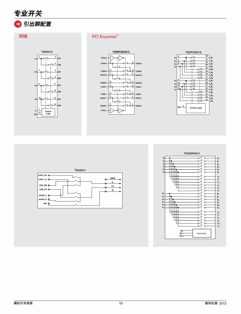
TS5N412
TxDA:0
TxDB:0
CTRL0
TxSA:0
TxSB:0
RxSA:0
RxSB:0
TxSA:1
TxSB:1
RxSA:1
RxSB:1
CTRL1
RxDA:0
TxDA:1
RxDB:0
TxDB:1
RxDB:1
RxDA:1
TS2PCIE2212
22
22
22
22
22
22
22
22
Network PCI Express®
0B1
1B1
2B1
3B1
0B2
1B2
2B2
3B2
4B1
5B1
6B1
7B1
4B2
5B2
6B2
7B2
A0
A1
A2
A3
A4
A5
A6
A7
2 38
3 37
6 36
7 35
34
33
32
31
11 29
12 2815 27
16 26
25
24
23
22
TS2PCIE412
SEL 9Control Logic
Specialty Switches
Pinouts
模拟开关指南 19 德州仪器 2012
专业开关
引出脚配置
网络 PCI Express®
20Analog Switch Guide Texas Instruments 2012
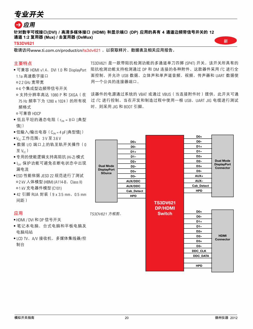
12-Ch 1:2 Mux/DeMux for DVI/HDMI and DP Applications w/4-Ch Sideband SwitchingTS3DV621
Get samples, data sheets and app reports at: www.ti.com/sc/device/ts3dv621
Key Features
and display port 1.1a high-speed digital interface
Wide bandwidth of 2.2 GHz Four integrated side band signals switching Support all video formats up to
at 75 Hz) HDCP compatible
(rON = 8 Ω typ)
(CON = 4 pF typ)
CC operating range from 3 V to 3.6 V
ports (0 to Vcc)
Hi-Z mode
OFF protection prevents current leakage in powered down state
2-kV human body model (A114B, Class II)
1-kV charged device model (C101)
0.5 mm pitch)
Applications
computers and docking stations
hubs/consoles
The TS3DV621 is a multiple SP4T switch with impedance detection. The switch features impedance detection, which supports the detection of various acces-sories that are attached through DP and DM. This device is fully controlled using I2C and enables USB data, stereo and mono audio, video, microphone, and UART data to use a common connector port.
Power for this device is supplied through VBAT of the system or through VBUS when attached. The switch can be controlled through I2
TS3DV621 block diagram.
Specialty Switches
Applications
Dual ModeDisplayPort
SOurce
Dual ModeDisplayPortConnector
D0+
D0–
D1+
D1–
D2+
D2–
D3+
D3–
AUX/DDC
AUX/DDC
Cab_Detect
HPD
D0+
D0–
D1+
D1–
D2+
D2–
D3+
D3–
AUX+
AUX–
Cab_Detect
HPD
HDMIConnector
D0+
D0–
D1+
D1–
D2+
D2–
D3+
D3–
DDC_CLK
DDC_DATA
HPD
TS3DV621DP/HDMI
Switch
模拟开关指南 20 德州仪器 2012
针对数字可视接口(DVI) / 高清多媒体接口 (HDMI) 和显示端口 (DP) 应用的具有 4 通道边频带信号开关的 12 通道 1:2 复用器 (Mux) / 去复用器 (DeMux) TS3DV621
专业开关
应用
主要特点
可兼容 HDMI v1.4、DVI 1.0 和 DisplayPort 1.1a 高速数字接口
2.2 GHz 宽带宽
4 个集成型边频带信号开关
支持分辨率高达 1080 P 和 SXGA(在 75 Hz 频率下为 1280 x 1024)的所有视
频格式
可兼容 HDCP 低且平坦的通态电阻(rON = 8Ω [典型
值])
低输入/输出电容(CON = 4 pF [典型值])
VCC 工作范围:3 V 至 3.6 V 数据 I/O 端口上的轨至轨开关操作(0 至 VCC)
专用的使能逻辑支持高阻抗 (Hi-Z) 模式
IOFF 保护功能可避免在断电状态中出现
漏电流
ESD 性能依据 JESD 22 规范进行了测试
2 kV 人体模型 (HBM) (A114-B,Class II) 1 kV 充电器件模型 (C101)
42 引脚 RUA 封装(9 x 3.5 mm,0.5 mm 间距)
应用
HDMI / DVI 和 DP 信号开关
笔记本电脑、台式电脑和平板电脑及
电脑坞站
LCD TV、A/V 接收机、多媒体集线器/控制台
敬请访问www.ti.com.cn/product/cn/ts3dv621 ,以获取样片、数据表及相关应用报告。
TS3DV621 是一款带阻抗检测功能的多通道单刀四掷 (SP4T) 开关。该开关所具有的
阻抗检测功能支持检测通过 DP 和 DM 连接的各种附件。这款器件采用 I2C 进行全
面控制,并允许 USB 数据、立体声和单声道音频、视频、传声器和 UART 数据使
用一个公共的连接器端口。
该器件的电源通过系统的 VBAT 或通过 VBUS(当连接附件时)提供。此开关可通
过 I2C 进行控制。当在开发和制造过程中使用一根 USB、UART JIG 电缆进行测试
时,则采用 JIG 和 BOOT 引脚。
新
TS3DV621 方框图。
21Analog Switch Guide Texas Instruments 2012
Key Features
(R,G,B, HSYNC, VSYNC, DDC CLK, and DDC DAT) integrated level shifting buffers for HSYNC and VSYNC
VDD = 3.3 V ± 10% VDD_5 = 5 V ± 10%
rON = 4 Ω (typ)
CON = 8 pF (typ)
SCL and SDA channels
(14 pins on port 1 and port 2) ±2-kV IEC61000-4-2, contact
discharge 7-kV human body model per
3-kV human body model per
(6 mm x 3 mm)
Applications
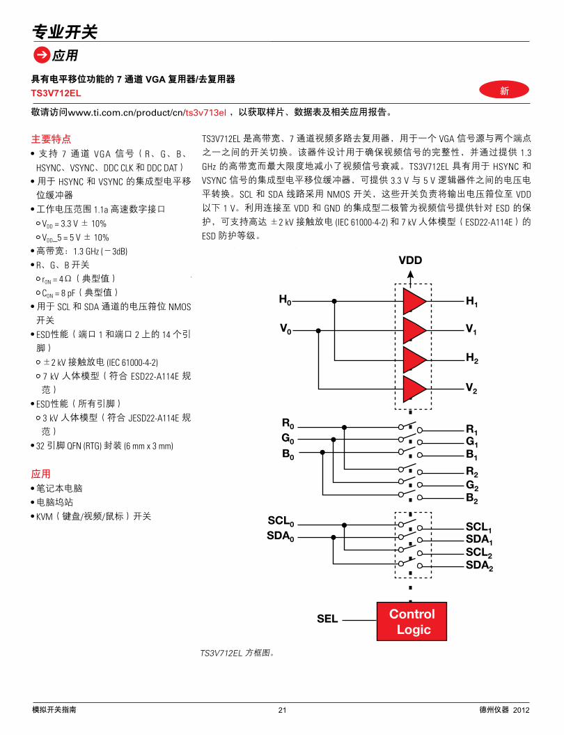
7-Channel VGA Mux/DeMux with Level ShiftingTS3V712EL
Get samples, data sheets, EVMs and app reports at: www.ti.com/sc/device/ts3v712el
The TS3V712EL is a high bandwidth, 7-channel video demultiplexer for switch-ing between a single VGA source and one of two end points. The device is designed for ensuring video signal integrity and minimizing video signal attenu-ation by providing high bandwidth of 1.3 GHz. The TS3V712EL has integrated level shifting buffers for the HSYNC and VSYNC signals which provide voltage level translation between 3.3 V and 5 V logic. The SCL and SDA lines use NMOS switches which clamp the output voltage to 1 V below VDD. The video signals are protected against ESD with integrated diodes to VDD and GND that support levels up to ±2-kV contact discharge (IEC61000-4-2) and 7-kV human body
Specialty Switches
Applications
TS3V712EL block diagram.
H1
VDD
V1
H0
V0
R0
G0
B0
G1
R1
B1
R2G2
SCL0
SDA0 SDA1
SCL1
SCL2SDA2
B2
H2
V2
SEL Control Logic
模拟开关指南 21 德州仪器 2012
具有电平移位功能的 7 通道 VGA 复用器/去复用器
TS3V712EL
专业开关
应用
主要特点
支持 7 通道 VGA 信号(R、G、B、
HSYNC、VSYNC、DDC CLK 和 DDC DAT)
用于 HSYNC 和 VSYNC 的集成型电平移
位缓冲器
工作电压范围 1.1a 高速数字接口
VDD = 3.3 V ± 10% VDD_5 = 5 V ± 10%
高带宽:1.3 GHz (-3dB) R、G、B 开关
rON = 4Ω(典型值)
CON = 8 pF(典型值)
用于 SCL 和 SDA 通道的电压箝位 NMOS 开关
ESD性能(端口 1 和端口 2 上的 14 个引
脚)
±2 kV 接触放电 (IEC 61000-4-2) 7 kV 人体模型(符合 ESD22-A114E 规范)
ESD性能(所有引脚)
3 kV 人体模型(符合 JESD22-A114E 规范)
32 引脚 QFN (RTG) 封装 (6 mm x 3 mm)
应用
笔记本电脑
电脑坞站
KVM(键盘/视频/鼠标)开关
敬请访问www.ti.com.cn/product/cn/ts3v713el ,以获取样片、数据表及相关应用报告。
TS3V712EL 是高带宽、7 通道视频多路去复用器,用于一个 VGA 信号源与两个端点
之一之间的开关切换。该器件设计用于确保视频信号的完整性,并通过提供 1.3 GHz 的高带宽而最大限度地减小了视频信号衰减。TS3V712EL 具有用于 HSYNC 和 VSYNC 信号的集成型电平移位缓冲器,可提供 3.3 V 与 5 V 逻辑器件之间的电压电
平转换。SCL 和 SDA 线路采用 NMOS 开关,这些开关负责将输出电压箝位至 VDD 以下 1 V。利用连接至 VDD 和 GND 的集成型二极管为视频信号提供针对 ESD 的保
护,可支持高达 ±2 kV 接触放电 (IEC 61000-4-2) 和 7 kV 人体模型(ESD22-A114E)的 ESD 防护等级。
新
TS3V712EL 方框图。
22Analog Switch Guide Texas Instruments 2012
The TS3L501E is a 16-bit to 8-bit multiplexer/demultiplexer LAN switch with a single select (SEL) input and Power down Mode input. The device provides additional I/Os for switching status indicating LED signals and includes high ESD protection. SEL in-put controls the data path of the multiplexer/demultiplexer. Power down input can put the device into the standby mode for minimizing current consumption per mode selection. The device provides a low and flat ON-state resistance (rON) and an excellent ON-state resistance match. Low input/output capacitance, high bandwidth, low skew, and low crosstalk among channels make this device suitable for various LAN appli-cations, such as 10/100/1000 Base-T. This device can be used to replace mechanical relays in LAN applications. It also can be used to route signals from a 10/100 Base-T Ethernet trans-
in laptops or in docking stations. It is characterized for operation over the free-air temperature range of –40ºC to 85ºC.
The TS3V713EL is a high bandwidth, 7-channel video multiplexer/demultiplexer for switching between a single VGA source and one of two end points. The device is designed for ensuring video signal integrity and minimizing video signal attenuation by providing high bandwidth of 1.3 GHz. The TS3V713EL has integrated level shifting buffers for the HSYNC and VSYNC signals which provide voltage level translation between 3.3 V and 5 V logic. The SCL and SDA lines use NMOS switches which clamp the output voltage to 1 V below VDD. The video signals are protected against ESD with integrated diodes to VDD and GND that support levels up to ±2-kV contact discharge (IEC61000-4-2) and 8-kV human
7-Channel 7:14 SPDT VGA Signal Switch with Level ShifterTS3V713EL
Get samples, data sheets and app reports at: www.ti.com/sc/device/ts3v713el
Key Features
(R,G,B, VSYNC, HSYNC, DDC1, DDC2
HSYNC, VSYNC
Applications
Specialty Switches
Applications
8:16 Mux/DeMux for Gigabit Ethernet LANTS3L501E
Get samples, data sheets and app reports at: www.ti.com/sc/device/ts3l501e
Key Features
(tSK(o) = 100 ps max)
rON = 4 Ω typ, rON(FLAT) = 0.5 Ω typ
CON = 8 pF typ
±4-kV IEC61000-4-2, contact discharge 6-kV human body model (HBM)
9 mm x 3.5 mm
Applications
signal switching
H1
V1
H0
V0
R0
G0
B0
G1
R1
B1
R2G2
SCL0
SDA0 SDA1
SCL1
SCL2SDA2
B2
H2
V2
SEL Control Logic
A0
A1A2
B1
B0
B2A3A4A5
B4
B3
B5A6
A7 B7
B6
C0
LED_A0
LED_A1LED_A2
LED_B1
LED_B0
LED_B2
C2
C1
C4C5
C3
C6C7
LED_C0LED_C1LED_C2
SEL Control Logic
PD Power Down
模拟开关指南 22 德州仪器 2012
具有电平移位器的 7 通道 7:14 单刀双掷 (SPDT) VGA 信号开关
TS3V713EL
适用于千兆位以太网 LAN 的 8:16 多路复用器/去复用器
TS3L501E
专业开关
应用
主要特点
高带宽:1.3 GHz(典型值)
用于 VGA 的 7 个通道(R、G、B、
VSYNC、HSYNC、DDC1、DDC2)
用于 HSYNC 和 VSYNC 的集成型电
平移位功能电路
I/O 电容:4 pF 与 pericom PI3V713 引脚对引脚兼容
应用
笔记本电脑
模拟 VGA 外设端口
显示屏 LVDS 总线多路复用器 (MUX) 视频/音频开关切换
高速逻辑数据 I / O 多路复用器 (MUX)
主要特点 低的位至位时滞 (b i t - to-b i t skew):(tSK(O) = 100ps [最大值]) 低且平坦的通态电阻
rON = 4Ω(典型值),rON(FLAT) = 0.5Ω(典型值)
低输入/输出电容 CON = 8 pF(典型值)
ESD 性能(A、B、C、LED 引脚) ±4 kV IEC 61000-4-2,接触放电 6 kV人体模型 (HBM)
42 引脚 QFN 封装 (RUA) - 9 mm x 3.5 mm,是同类竞争产品的一半 可提供低功率损失与总谐波失真 (THD) 低电容可确保极大的信号带宽 (BW) 免除了增设外部 ESD 组件的需要 尺寸比 TS3L500AE 缩小了 37%
应用 10/100/1000 Base-T 信号开关切换 差分(LVDS、LVPECL)信号开关切换 音频/视频开关切换 集线器和路由器信号开关切换
敬请访问www.ti.com.cn/product/cn/ts3I501e ,以获取样片、数据表及相关应用报告。
敬请访问www.ti.com.cn/product/cn/ts3I501e ,以获取样片、数据表及相关应用报告。
TS3V713EL 是一款高带宽、7 通道视频多路
复用器/去复用器,用于一个 VGA 信号源与
两个端点之一之间的开关切换。该器件设
计用于确保视频信号的完整性,并通过提
供 1.3 GHz 的高带宽而最大限度地减小了视
频信号衰减。TS3V713EL 具有用于 HSYNC 和 VSYNC 信号的集成型电平移位缓冲器,可
提供 3.3 V 与 5 V 逻辑器件之间的电压电平
转换。SCL 和 SDA 线路采用 NMOS 开关,
这些开关负责将输出电压箝位至 VDD 以下 1 V。利用连接至 VDD 和 GND 的集成型二极
管为视频信号提供针对 ESD 的保护,可支
持高达 ±2 kV 接触放电 (IEC 61000-4-2) 和 8 kV 人体模型(ESD22-A114E)的 ESD 防护等
级。
TS3L501E 是一款 16 位至 8 位多路复用器/去复用器 LAN 开关,具有单个选择 (SEL) 输入和断电模式输入。该器件提供了用于开关状态指示 LED 信号的额外 I/O,并
拥有很高的 ESD 保护等级。SEL 输入负责控制多路复用器/去复用器的数据通路。
断电输入能够将器件置于待机模式之中,以借助模式选择来最大限度地降低电流
新
消耗。该器件提供了低且平坦的通
态电阻 (rON) 和卓越的通态电阻匹配
性能。低输入/输出电容、高带宽、
低时滞以及通道之间的低串扰使得
这款器件适合于各种不同的 LAN 应用,例如:10/100/1000 Base-T。该器
件可用于替代 LAN 应用中的机械式
继电器。另外,其还能用于将信号
从一个 10/100 Base-T 以太网收发器路
由至笔记本电脑或电脑坞站中的 RJ-45 LAN 连接器。TS3L501E 针对 -40ºC 至 85ºC的自然通风工作温度范围进
行了特性分析。
23Analog Switch Guide Texas Instruments 2012
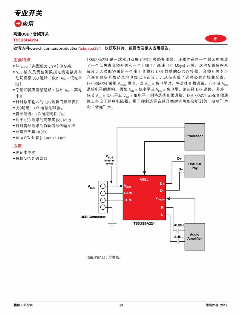
The TS5USBA224 is a double-pole, double throw (DPDT) multiplexer that includes a low-distortion audio switch and a USB 2.0 High-Speed (480 Mbps) switch in the same package. This configuration allows the system designer to use a common connector for audio and USB data. The audio switch is designed to allow audio signals to swing below ground which makes this common connector configura-tion possible. The TS5USBA224 is powered up using VAUDIO. When ASEL=High, the audio path is selected regardless of the logic level at VBUS. If ASEL=Low and VBUS=High, the USB path is selected. Otherwise if ASEL=Low and VBUS=Low, the audio path is selected. The TS5USBA224 also features shunt resistors on the audio path to reduce clicks and pops that may be heard when the audio switches are selected.
High-Speed USB/Audio SwitchTS5USBA224
Get samples, data sheets and app reports at: www.ti.com/sc/device/ts5usba224
Key Features
AUDIO (3.3 V typ)
BUS input detects data cable connection and automatically switches to USB path (if ASEL = L)
(if ASEL = H)
for digital inputs
ON
ON
path
audio path
Applications
Specialty Switches
Applications
ASEL
VBUSVBUS
VAudio
D+/R
D–/L
D+
D–
D+
AUDR
AUDL
D–
R
L
VBUSdirect to device
USB Connector
TS5USBA224
Processor
AudioAmplifier
USB 2.0Phy
TS5USBA224 block diagram.
模拟开关指南 23 德州仪器 2012
高速USB / 音频开关
TS5USBA224
专业开关
应用
主要特点
从 VAUDIO(典型值为 3.3 V)来供电
VBUS 输入负责检测数据电缆连接并自
动切换至 USB 通路(假如 ASEL = 低电平 [L])
手动切换至音频通路(假如 ASEL = 高电
平 [H])
针对数字输入的 1.8 V逻辑门限兼容性
USB通道:4Ω 通态电阻 (RON) 音频通道:3Ω 通态电阻 (RON) 用于 USB 通路的高带宽 (650 MHz) 针对音频通路的负轨信号传输支持
总谐波失真< 0.05% 10-μQFN 封装 (1.8 mm x 1.4 mm)
应用
笔记本电脑
模拟 VGA 外设端口
敬请访问www.ti.com.cn/product/cn/ts5usba224,以获取样片、数据表及相关应用报告。
TS5USBA224 是一款双刀双掷 (DPDT) 多路复用器,该器件在同一个封装中集成
了一个低失真音频开关和一个 USB 2.0 高速 (480 Mbps) 开关。这种配置使得系
统设计人员能够采用一个用于音频和 USB 数据的公共连接器。音频开关专为
允许音频信号摆动至地电位以下而设计,从而实现了这种公共连接器配置。
TS5USBA224 采用 VAUDIO 供电。当 ASEL = 高电平时,将选择音频通路,而不受 VBUS 逻辑电平的影响。假如 ASEL = 低电平且 VBUS = 高电平,则选择 USB 通路。另外,
倘若 ASEL = 低电平且 VBUS = 低电平,则将选择音频通路。TS5USBA224 还在音频通
路上布设了并联电阻器,用于抑制选择音频开关时有可能会听到的“喀呖”声
和“劈啪”声。
新
TS5USBA224 方框图。
24Analog Switch Guide Texas Instruments 2012
High-Speed 2:4 Differential Multiplexer / De-multiplexer TS3DS10224
Get samples, data sheets and app reports at: www.ti.com/sc/device/ts3ds10224
Key Features
Single 1 to 4 Dual 1 to 2 Fan-out 1 to 2
ON and CON: 10 Ω rON typ 8 pF CON typ
±8-kV contact discharge (IEC61000-4-2) 2-kV human body model per
2-kV human body model per
(3 x 3, 0.4-mm pitch)
Applications
channel multiplexing
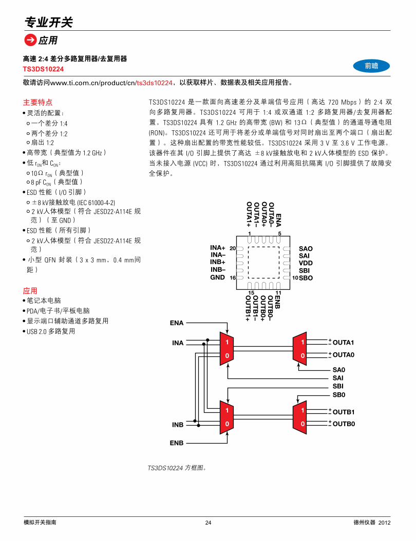
The TS3DS10224 is a 2:4 bidirectional multiplexer for high-speed differential and single ended signal applications (up to 720 Mbps). The TS3DS10224 can be used in a 1:4 or dual 1:2 multiplexer/demultiplexer configuration. The TS3DS10224 of-fers a high BW of 1.2 GHz with channel RON of 13 Ω (typ). The TS3DS10224 can also be used to fan out a differential or single ended signal pair to two portssimultaneously (fan-out configuration). The BW performance is lower in this con-figuration. The TS3DS10224 operates with a 3 to 3.6V power supply. It features ESD protection of up to ±8-kV contact discharge and 2-kV human body model on its I/O pins. The TS3DS10224 provides fail-safe protection by isolating the I/O pins with high impedance when the power supply (VCC) is not present.
Specialty Switches
Applications
EN
A
ENA
OUTA1
OUTA0
SA0SAISBISB0
ENB
INB
INA
OUTB0
OUTB1
OU
TA0–
OU
TA0+
OU
TA1–
OU
TA1+
EN
BO
UT
B0–
OU
TB
0+O
UT
B1–
OU
TB
1+
INA+ 20
16
1 5
15 11
10
INA–INB+INB–GND
SAOSAIVDDSBISBO
+–
+–
+–+–
1
0
1
0
1
0
1
0
TS3DS10224 block diagram.
模拟开关指南 24 德州仪器 2012
高速 2:4 差分多路复用器/去复用器
TS3DS10224
专业开关
应用
主要特点
灵活的配置:
一个差分 1:4 两个差分 1:2 扇出 1:2
高带宽(典型值为 1.2 GHz)
低 rON和 CON:
10Ω rON(典型值) 8 pF CON(典型值)
ESD 性能(I/O 引脚)
±8 kV接触放电 (IEC 61000-4-2) 2 kV人体模型(符合 JESD22-A114E 规范)(至 GND)
ESD 性能(所有引脚)
2 kV人体模型(符合 JESD22-A114E 规范)
小型 QFN 封装(3 x 3 mm,0.4 mm间
距)
应用 笔记本电脑
PDA/电子书/平板电脑
显示端口辅助通道多路复用
USB 2.0 多路复用
敬请访问www.ti.com.cn/product/cn/ts3ds10224,以获取样片、数据表及相关应用报告。
TS3DS10224 是一款面向高速差分及单端信号应用(高达 720 Mbps)的 2:4 双向多路复用器。TS3DS10224 可用于 1:4 或双通道 1:2 多路复用器/去复用器配
置。TS3DS10224 具有 1.2 GHz 的高带宽 (BW) 和 13Ω(典型值)的通道导通电阻 (RON)。TS3DS10224 还可用于将差分或单端信号对同时扇出至两个端口(扇出配
置)。这种扇出配置的带宽性能较低。TS3DS10224 采用 3 V 至 3.6 V 工作电源。
该器件在其 I/O 引脚上提供了高达 ±8 kV接触放电和 2 kV人体模型的 ESD 保护。
当未接入电源 (VCC) 时,TS3DS10224 通过利用高阻抗隔离 I/O 引脚提供了故障安
全保护。
前瞻
TS3DS10224 方框图。
25Analog Switch Guide Texas Instruments 2012
DP3T USB 2.0 High-Speed (480 Mbps) and Audio Switches with NegativeSignal Capability TS3USBA225
Get samples, data sheets and app reports at: www.ti.com/sc/device/ts3uba225
Key Features
(D0± and D1 ±) 6.5 Ω RDSON maximum 3 pF CON maximum 1.9 GHz bandwidth (-3 dB) VI/O accepts signals up to 4.3 V (independent of VCC)
2.5 Ω RDSON typical Negative rail capability Low THD: <0.05% Internal shunt resistors for click-and-pop reduction
(VCC)
(SEL1 and SEL2) threshold
(~2 µA) in power-down mode
high-Z when VCC=0V
2000-V human body model (A114-B, Class II) 1000 V charged device model (C101)
2×1.7 mm, 0.4 mm pitch
Applications
The TS3USBA225 is a double-pole, triple throw (DP3T) multiplexer that includes a low-distortion audio switch, and two USB 2.0 High-Speed (480 Mbps) switches in the same package. This configuration allows the system designer to use a common connector for audio, and USB data. The audio switch is designed to allow audiosignals to swing negatively which makes this common connector configuration possible. The TS3USBA225 has a VCC range of 2.7 V to 4.3 V with the capability to pass true-ground audio signals down to VCC-4.3 V. The device also supports a power-down mode that can be enabled when both SEL controls are low to minimize current consumption when no signal is transmitting. The TS3USBA225 also features internal shunt resistors on the audio path to reduce clicks and pops that may be heard when the audio switches are selected.
Specialty Switches
Applications
1
2
3
4
5
11
10
8
9
76
12
Top ViewL
GND
D–/R
D+/L
SEL2
SEL1D1+D0+
VCC
D1–
D0–
R
D+/L
D–/R
SEL2SEL1
D0+D1+L
D0–D1–R
VCC RSHUNT
Rpd1 Rpd2
RSHUNT
Control Logic
模拟开关指南 25 德州仪器 2012
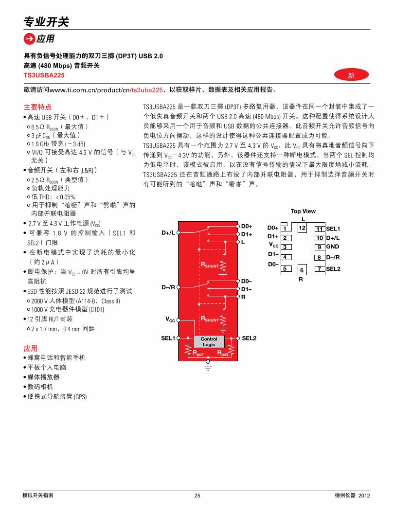
具有负信号处理能力的双刀三掷 (DP3T) USB 2.0 高速 (480 Mbps) 音频开关
TS3USBA225
专业开关
应用
主要特点
高速 USB 开关(D0±,D1±)
6.5Ω RDSON(最大值) 3 pF CON(最大值) 1.9 GHz 带宽 (-3 dB) VI/O 可接受高达 4.3 V 的信号(与 VCC 无关)
音频开关(左和右 [L&R])
2.5Ω RDSON(典型值) 负轨处理能力 低 THD:< 0.05% 用于抑制“喀呖”声和“劈啪”声的内部并联电阻器
2.7 V 至 4.3 V 工作电源 (VCC) 可兼容 1 .8 V 的控制输入(SEL1 和 SEL2)门限
在断电模式中实现了流耗的最小化
(约 2μA)
断电保护:当 VCC = 0V 时所有引脚均呈
高阻抗
ESD 性能按照 JESD 22 规范进行了测试
2000 V 人体模型 (A114-B,Class II) 1000 V 充电器件模型 (C101)
12 引脚 RUT 封装
2 x 1.7 mm,0.4 mm 间距
应用 蜂窝电话和智能手机
平板个人电脑
媒体播放器
数码相机
便携式导航装置 (GPS)
敬请访问www.ti.com.cn/product/cn/ts3uba225,以获取样片、数据表及相关应用报告。
TS3USBA225 是一款双刀三掷 (DP3T) 多路复用器,该器件在同一个封装中集成了一
个低失真音频开关和两个 USB 2.0 高速 (480 Mbps) 开关。这种配置使得系统设计人
员能够采用一个用于音频和 USB 数据的公共连接器。此音频开关允许音频信号向
负电位方向摆动,这样的设计使得这种公共连接器配置成为可能。
TS3USBA225 具有一个范围为 2.7 V 至 4.3 V 的 VCC,此 VCC 具有将真地音频信号向下
传递到 VCC-4.3V 的功能。另外,该器件还支持一种断电模式,当两个 SEL 控制均
为低电平时,该模式被启用,以在没有信号传输的情况下最大限度地减小流耗。
TS3USBA225 还在音频通路上布设了内部并联电阻器,用于抑制选择音频开关时
有可能听到的“喀哒”声和“噼啪”声。
新
26Analog Switch Guide Texas Instruments 2012
DPDT MHLTM (3 Gbps) and USB 2.0 High-Speed (480 Mbps) Switch with Integrated ID line MuxTS3USB3200
Get samples, data sheets and app reports at: www.ti.com/sc/device/ts3usb3200
Key Features
Supports 5 Gbps data rate High bandwidth of 6 GHz 2.5 pF CON typical
6 GHz Bandwidth (-3 dB) 3.0 pF CON
(SEL1 and SEL2) threshold
for easy information control
(<~30uA) during normal operation
powered by VBUS without VCC
I/O pins up to 5.5 V without external components
2000-V human body model (A114-B, Class II) 1000-V charged device model
(C101)
2.6×1.8 mm, 0.4 mm pitch
Applications
The TS3USB3200 is a Double-Pole, Double Throw (DPDT) multiplexer that includes a high-speed Mobile High-Definition Link (MHL) switch and an USB 2.0 high-speed (480Mbps) switches in the same package. Also included is a Single-Pole, Double Throw (SPDT) USB/MHL ID switch for easy information control. These configurations allow the system designer to use a common USB or Micro-USB connector for both MHL video signals and USB data.
The TS3USB3200 has a VCC range of 2.7 V to 4.3 V and also has the option to be powered by VBUS alone without VCC. This device supports Over-Voltage Tolerance (OVT) feature, which allows the I/O pins to withstand over-voltage conditions (up to 5.5 V). The power-off protection feature forces all I/O pins to be in high-impedance mode when power is not present, allowing full isolation of the signals lines under such condition without excessive leakage current. The select pins of TS3USB3200 are compatible with 1.8 V control voltage, allowing them to be directly interfaced with the General Purpose I/O (GPIO) from a mobile processor.
The TS3USB3200 comes with a small 16-pin QFN package with only 2.6 mm x 1.8 mm in size, which makes it a perfect candidate to be used in mobile applications.
Specialty Switches
Applications
D+
PSELVBUS
USB+
MHL+
D+USB–
MHL–
D+ID_MHL
ID_USB
SwitchPower
SEL2SEL1 Control Logic
ID_M
HL
ID_C
OM
VB
US
VC
C
GN
D
US
B+
US
B–
SE
L1
GND
1 5
D+
D–
PSEL
ID_USB
MHL+
MHL–
SEL2
1
2
3
4
12
11
10
9
16 15 14 13
55 6 7 8
模拟开关指南 26 德州仪器 2012
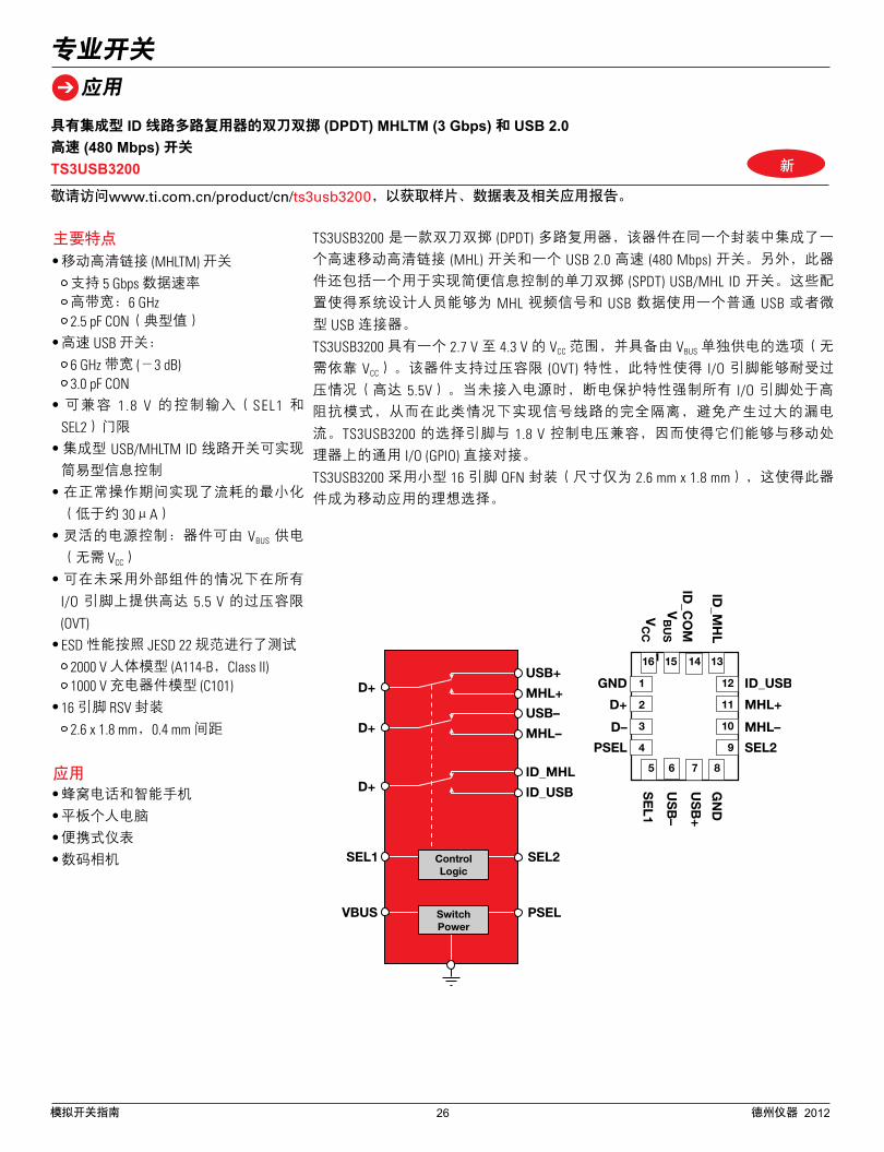
具有集成型 ID 线路多路复用器的双刀双掷 (DPDT) MHLTM (3 Gbps) 和 USB 2.0 高速 (480 Mbps) 开关
TS3USB3200
专业开关
应用
主要特点
移动高清链接 (MHLTM) 开关
支持 5 Gbps 数据速率 高带宽:6 GHz 2.5 pF CON(典型值)
高速 USB 开关:
6 GHz 带宽 (-3 dB) 3.0 pF CON
可兼容 1 .8 V 的控制输入(SEL1 和 SEL2)门限
集成型 USB/MHLTM ID 线路开关可实现
简易型信息控制
在正常操作期间实现了流耗的最小化
(低于约 30μA)
灵活的电源控制:器件可由 VBUS 供电
(无需 VCC)
可在未采用外部组件的情况下在所有 I/O 引脚上提供高达 5.5 V 的过压容限 (OVT) ESD 性能按照 JESD 22 规范进行了测试
2000 V 人体模型 (A114-B,Class II) 1000 V 充电器件模型 (C101)
16 引脚 RSV 封装
2.6 x 1.8 mm,0.4 mm 间距
应用 蜂窝电话和智能手机
平板个人电脑
便携式仪表
数码相机
敬请访问www.ti.com.cn/product/cn/ts3usb3200,以获取样片、数据表及相关应用报告。
TS3USB3200 是一款双刀双掷 (DPDT) 多路复用器,该器件在同一个封装中集成了一
个高速移动高清链接 (MHL) 开关和一个 USB 2.0 高速 (480 Mbps) 开关。另外,此器
件还包括一个用于实现简便信息控制的单刀双掷 (SPDT) USB/MHL ID 开关。这些配
置使得系统设计人员能够为 MHL 视频信号和 USB 数据使用一个普通 USB 或者微
型 USB 连接器。
TS3USB3200 具有一个 2.7 V 至 4.3 V 的 VCC 范围,并具备由 VBUS 单独供电的选项(无
需依靠 VCC)。该器件支持过压容限 (OVT) 特性,此特性使得 I/O 引脚能够耐受过
压情况(高达 5.5V)。当未接入电源时,断电保护特性强制所有 I/O 引脚处于高
阻抗模式,从而在此类情况下实现信号线路的完全隔离,避免产生过大的漏电
流。TS3USB3200 的选择引脚与 1.8 V 控制电压兼容,因而使得它们能够与移动处
理器上的通用 I/O (GPIO) 直接对接。
TS3USB3200 采用小型 16 引脚 QFN 封装(尺寸仅为 2.6 mm x 1.8 mm),这使得此器
件成为移动应用的理想选择。
新
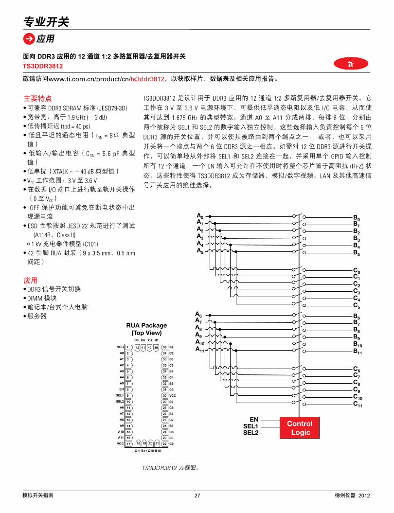
27Analog Switch Guide Texas Instruments 2012
12-channel 1:2 Mux/Demux for DDR3 ApplicationsTS3DDR3812
Get samples, data sheets and app reports at: www.ti.com/sc/device/ts3ddr3812
Key Features
(rON = 8 Ω typ)
(CON = 5.6 pF typ)
CC operating range from 3 V to 3.6 V
Ports (0 to VCC)
OFF protection prevents current leakage in powered-down state
2-kV human body model (A114B, Class II) 1-kV charged device model (C101)
(9 x 3.5 mm, 0.5 mm pitch)
Applications
The TS3DDR3812 is a 12-channel, 1:2 multiplexer/demultiplexer switch designed for DDR3 applications. It operates from a 3 to 3.6 V supply and offers low and flat ON-state resistance as well as low I/O capacitance which allow it to achieve a typical bandwidth of 1.675 GHz. Channels A0 through A11 are divided into two banks of six bits and are independently controlled via two digital inputs called SEL1 and SEL2. These select inputs control the switch position of each 6-bit DDR3 source and allow them to be routed to one of two end-points. Alternatively, the switch can be used to connect a single endpoint to one of two 6-bit DDR3 sources. For switching 12-bit DDR3 sources, simply connect SEL1 and SEL2 together externally and control all 12 channels with a single GPIO input. An EN input allows the entire chip to be placed into a high-impedance (Hi-Z) state while not in use. These characteristics make the TS3DDR3812 an excellent choice for use in memory, analog/digital video, LAN, and other high-speed signal switching applications.
Specialty Switches
Applications
TS3DDR3812 block diagram.
B0B1B2B3B4B5
C0C1C2C3C4C5
A0A1A2A3A4A5
B6B7B8B9B10B11
C6C7C8C9C10C11
A6
ENSEL1SEL2
A7A8A9A10A11
38
37
36
35
34
33
32
31
30
29
28
27
26
25
24
23
22
B2
C2
B3
C3
B4
C4
B5
C5
VCC
B6
C6
B7
C7
B8
C8
B9
C9
VCC
C0 B0
RUA Package(Top View)
C1 B1
A0
A1
A2
A3
A4
A5
EN
SEL1
SEL2
A6
A7
A8
A9
A10
A11
VCC
1
2
3
4
5
6
7
8
9
10
11
12
13
14
15
16
17 18 19 20 21
42 41 40 39
C11 B11 C10 B10
Control Logic
模拟开关指南 27 德州仪器 2012
面向 DDR3 应用的 12 通道 1:2 多路复用器/去复用器开关
TS3DDR3812
专业开关
应用
主要特点 可兼容 DDR3 SDRAM 标准 (JESD79-3D) 宽带宽:高于 1.9 GHz (-3 dB) 低传播延迟 (tpd = 40 ps) 低且平坦的通态电阻(rON = 8Ω 典型值)
低输入/输出电容(CON = 5.6 pF 典型值)
低串扰(XTALK = -43 dB 典型值)
VCC 工作范围:3 V 至 3.6 V 在数据 I/O 端口上进行轨至轨开关操作(0 至 VCC)
IOFF 保护功能可避免在断电状态中出现漏电流
ESD 性能按照 JESD 22 规范进行了测试 (A114B,Class II) 1 kV 充电器件模型 (C101)
42 引脚 RUA 封装(9 x 3.5 mm,0.5 mm 间距)
应用 DDR3 信号开关切换
DIMM 模块
笔记本/台式个人电脑
服务器
敬请访问www.ti.com.cn/product/cn/ts3ddr3812,以获取样片、数据表及相关应用报告。
TS3DDR3812 是设计用于 DDR3 应用的 12 通道 1:2 多路复用器/去复用器开关。它
工作在 3 V 至 3.6 V 电源环境下,可提供低平通态电阻以及低 I/O 电容,从而使
其可达到 1.675 GHz 的典型带宽。通道 A0 至 A11 分成两排,每排 6 位,分别由
两个被称为 SEL1 和 SEL2 的数字输入独立控制。这些选择输入负责控制每个 6 位 DDR3 源的开关位置,并可以使其被路由到两个端点之一。 或者,也可以采用
开关将一个端点与两个 6 位 DDR3 源之一相连。如需对 12 位 DDR3 源进行开关操
作,可以简单地从外部将 SEL1 和 SEL2 连接在一起,并采用单个 GPIO 输入控制
所有 12 个通道。一个 EN 输入可允许在不使用时将整个芯片置于高阻抗 (Hi-Z) 状态。这些特性使得 TS3DDR3812 成为存储器、模拟/数字视频、LAN 及其他高速信
号开关应用的绝佳选择。
新
TS3DDR3812 方框图。
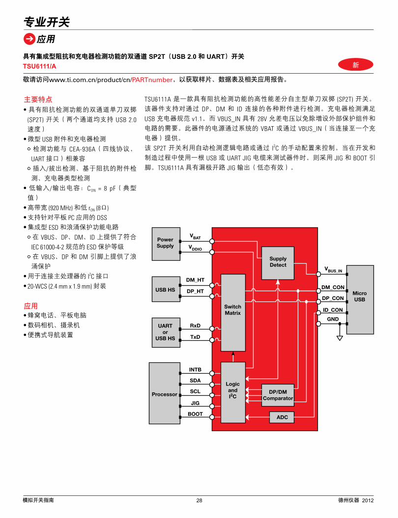
28Analog Switch Guide Texas Instruments 2012
Specialty Switches
Applications
Dual SP2T (USB2.0 and UART) with Integrated Impedance and Charger DetectionTSU6111/A
Get samples, data sheets and app reports at: www.ti.com/sc/device/PARTnumber
Key Features
support USB2.0 speed) with impedance detection
detection
Detection is compatible with CEA-936A (4-Wire Protocol, UART interface) Plugin/unplug detection, impedance based accessory detection, charger type detection
CON=8pF typ.
rON (8 Ω)
application
IEC61000-4-2 ESD protection on VBUS, DP, DM, ID Surge protection on VBUS, DP
and DM pins2C interface with host processor
Applications
The TSU6111A is a high performance differential autonomous SP2T switch with impedance detection. The switch supports the detection of various accessories that are attached through DP, DM, and ID. The charger detection satisfies USB charger specification v1.1 and VBUS_IN has a 28 V tolerance to eliminate the need for external protection. Power for this device is supplied through VBAT of the system or through VBUS_IN when attached to a charger.
The SP2T switch is controlled by the automatic detection logic or through manual configuration of the I2
cable is used to test the device in the development and manufacturing. TSU6111A
MicroUSB
Power Supply
VBAT
VBUS_IN
VDDIO
DM_HTDM_CON
DP_CON
ID_CON
GND
DP_HT
RxD
TxD
INTB
SDA
SCL
JIG
BOOT
Processor
USB HS
UARTor
USB HS
SwitchMatrix
DP/DMComparator
ADC
SupplyDetect
LogicandI2C
模拟开关指南 28 德州仪器 2012
具有集成型阻抗和充电器检测功能的双通道 SP2T(USB 2.0 和 UART)开关
TSU6111/A
专业开关
应用
主要特点
具有阻抗检测功能的双通道单刀双掷 (SP2T) 开关(两个通道均支持 USB 2.0 速度)
微型 USB 附件和充电器检测
检测功能与 CEA-936A(四线协议,
UART 接口)相兼容
插入/拔出检测、基于阻抗的附件检
测、充电器类型检测
低输入/输出电容:CON = 8 pF(典型
值)
高带宽 (920 MHz) 和低 rON (8Ω) 支持针对平板 PC 应用的 DSS 集成型 ESD 和浪涌保护功能电路
在 VBUS、DP、DM、ID 上提供了符合 IEC 61000-4-2 规范的 ESD 保护等级
在 VBUS、DP 和 DM 引脚上提供了浪
涌保护
用于连接主处理器的 I2C 接口
20-WCS (2.4 mm x 1.9 mm) 封装
应用 蜂窝电话、平板电脑
数码相机、摄录机
便携式导航装置
敬请访问www.ti.com.cn/product/cn/PARTnumber,以获取样片、数据表及相关应用报告。
TSU6111A 是一款具有阻抗检测功能的高性能差分自主型单刀双掷 (SP2T) 开关。
该器件支持对通过 DP、DM 和 ID 连接的各种附件进行检测。充电器检测满足 USB 充电器规范 v1.1,而 VBUS_IN 具有 28V 允差电压以免除增设外部保护组件和
电路的需要。此器件的电源通过系统的 VBAT 或通过 VBUS_IN(当连接至一个充
电器)提供。
该 SP2T 开关利用自动检测逻辑电路或通过 I2C 的手动配置来控制。当在开发和
制造过程中使用一根 USB 或 UART JIG 电缆来测试器件时,则采用 JIG 和 BOOT 引脚。TSU6111A 具有漏极开路 JIG 输出(低态有效)。
新
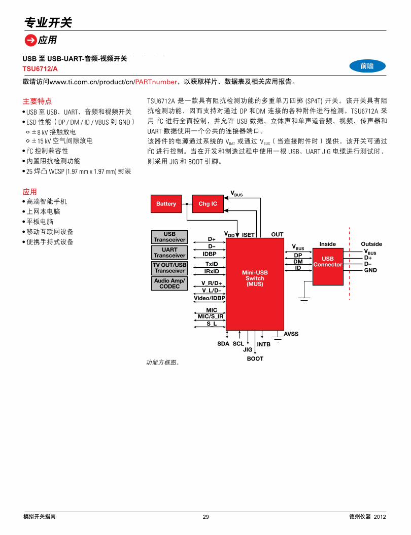
29Analog Switch Guide Texas Instruments 2012
USB to USB-UART-Audio-Video SwitchTSU6712/A
Get samples, data sheets and app reports at: www.ti.com/sc/device/PARTnumber
Key Features
video
to GND ±8-kV contact discharge ±15-kV air gap discharge
2C control compatibility
(1.97 mm × 1.97 mm) Package
Applications
The TSU6712A is a multiple SP4T switch with impedance detection. The switch features impedance detection, which supports the detection of various accessories that are attached through DP and DM. The TSU6712A is fully controlled using I2C and enables USB data, stereo and mono audio, video, microphone, and UART data to use a common connector port.
Power for this device is supplied through VBAT of the system or through VBUS when attached. The switch can be controlled through I2
Specialty Switches
Applications
Functional block diagram.
USBTransceiver
VBUS
OUTISETVDD
VBUS
VBUS
D+D–GND
Inside Outside
DPDMID
UARTTransceiver
TV OUT/USBTransceiver
Audio Amp/CODEC
Mini-USBSwitch (MUS)
USBConnector
Battery Chg IC
V_R/D+V_L/D–
Video/IDBP
TxIDIRxID
D+D–
IDBP
MICMIC/S_IR
S_L
SDA SCLJIG
BOOT
INTB
AVSS
模拟开关指南 29 德州仪器 2012
USB 至 USB-UART-音频-视频开关
TSU6712/A
专业开关
应用
主要特点
USB 至 USB、UART、音频和视频开关
ESD 性能(DP / DM / ID / VBUS 到 GND)
±8 kV 接触放电 ±15 kV 空气间隙放电
I2C 控制兼容性
内置阻抗检测功能
25 焊凸 WCSP (1.97 mm x 1.97 mm) 封装
应用 高端智能手机
上网本电脑
平板电脑
移动互联网设备
便携手持式设备
敬请访问www.ti.com.cn/product/cn/PARTnumber,以获取样片、数据表及相关应用报告。
TSU6712A 是一款具有阻抗检测功能的多重单刀四掷 (SP4T) 开关。该开关具有阻
抗检测功能,因而支持对通过 DP 和DM 连接的各种附件进行检测。TSU6712A 采用 I2C 进行全面控制,并允许 USB 数据、立体声和单声道音频、视频、传声器和 UART 数据使用一个公共的连接器端口。 该器件的电源通过系统的 VBAT 或通过 VBUS(当连接附件时)提供。该开关可通过 I2C 进行控制。当在开发和制造过程中使用一根 USB、UART JIG 电缆进行测试时,
则采用 JIG 和 BOOT 引脚。
前瞻
功能方框图。
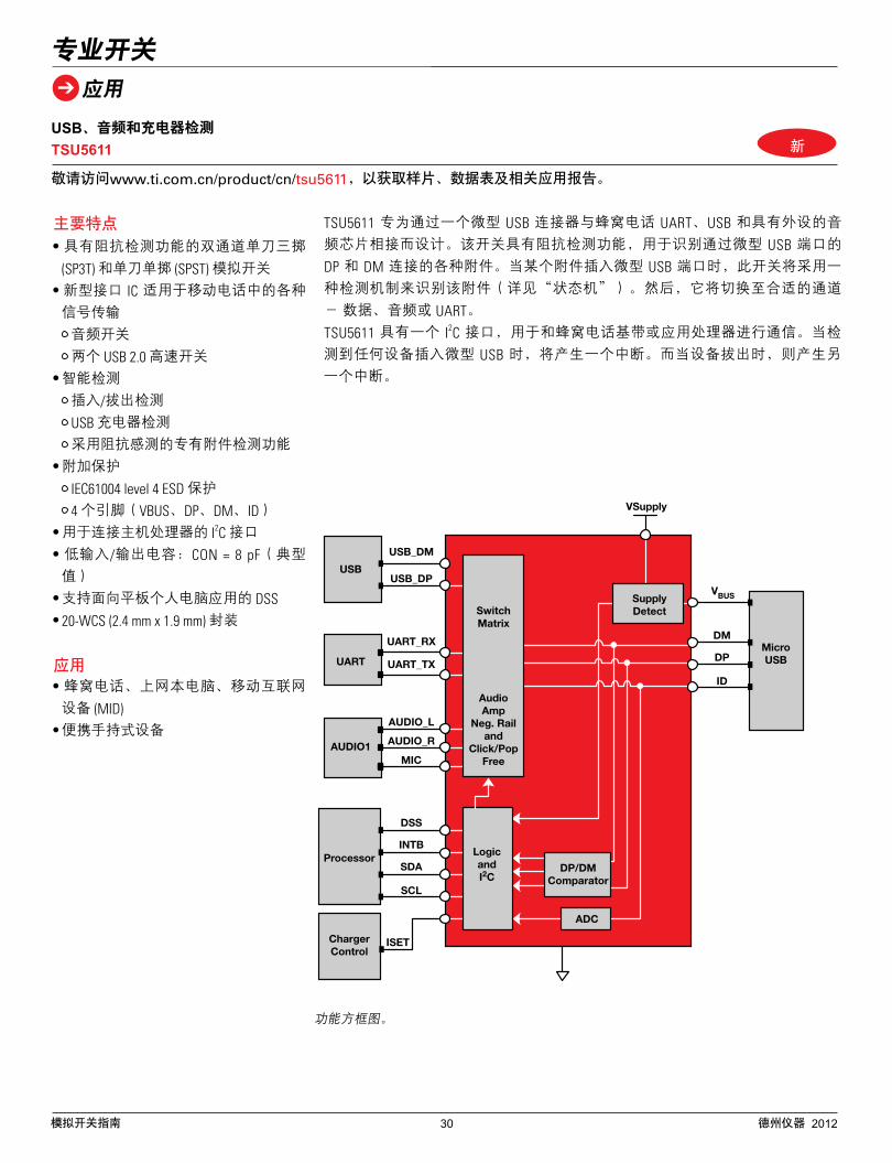
30Analog Switch Guide Texas Instruments 2012
USB, Audio, and Charger detectionTSU5611
Get samples, data sheets and app reports at: www.ti.com/sc/device/tsu5611
Key Features
with impedance detection.
in mobile phones Audio switch Two USB 2.0 high-speed switch
Plug-in/un-plug detection USB charger detection Proprietary accessory detection with impedance sensing
IEC61004 level 4 ESD protection 4pins (VBUS, DP,DM, ID)
2C interface with host processor
CON=8pF typ.
application
Applications
The TSU5611 is designed to interface the cellular phone UART, USB, and audio chips with external peripherals via a micro-USB connector. The switch features impedance detection for identification of various accessories that are attached through DP and DM of the micro-USB port. When an accessory is plugged into the micro-USB port, the switch uses a detection mechanism to identify the accessory (see the State Machine for details). It will then switch to the appropriate channel—data, audio, or UART.
The TSU5611 has an I2C interface for communication with the cellular phone baseband or applications processor. An interrupt is generated when anything plugged into the micro-USB is detected. Another interrupt is generated when the device is unplugged.
Specialty Switches
Applications
MicroUSB
USB
USB_DM
VBUS
VSupply
USB_DP
UART_RX DM
DP
ID
UART_TX
AUDIO_L
AUDIO_R
DSS
INTB
SDA
SCL
ISET
Processor
ChargerControl
UART
AUDIO1
LogicandI2C
MIC
SwitchMatrix
AudioAmp
Neg. Railand
Click/PopFree
DP/DMComparator
ADC
SupplyDetect
Functional block diagram.
模拟开关指南 30 德州仪器 2012
USB、音频和充电器检测
TSU5611
专业开关
应用
主要特点
具有阻抗检测功能的双通道单刀三掷 (SP3T) 和单刀单掷 (SPST) 模拟开关
新型接口 IC 适用于移动电话中的各种
信号传输
音频开关
两个 USB 2.0 高速开关
智能检测
插入/拔出检测
USB 充电器检测
采用阻抗感测的专有附件检测功能
附加保护
IEC61004 level 4 ESD 保护
4 个引脚(VBUS、DP、DM、ID)
用于连接主机处理器的 I2C 接口
低输入/输出电容:CON = 8 pF(典型
值)
支持面向平板个人电脑应用的 DSS 20-WCS (2.4 mm x 1.9 mm) 封装
应用 蜂窝电话、上网本电脑、移动互联网
设备 (MID) 便携手持式设备
敬请访问www.ti.com.cn/product/cn/tsu5611,以获取样片、数据表及相关应用报告。
TSU5611 专为通过一个微型 USB 连接器与蜂窝电话 UART、USB 和具有外设的音
频芯片相接而设计。该开关具有阻抗检测功能,用于识别通过微型 USB 端口的 DP 和 DM 连接的各种附件。当某个附件插入微型 USB 端口时,此开关将采用一
种检测机制来识别该附件(详见“状态机”)。然后,它将切换至合适的通道 - 数据、音频或 UART。
TSU5611 具有一个 I2C 接口,用于和蜂窝电话基带或应用处理器进行通信。当检
测到任何设备插入微型 USB 时,将产生一个中断。而当设备拔出时,则产生另
一个中断。
新
功能方框图。
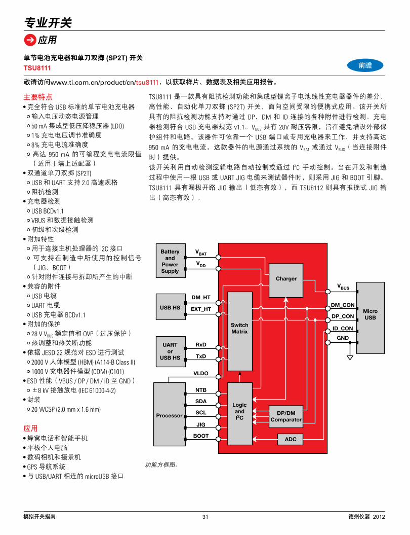
31Analog Switch Guide Texas Instruments 2012
Specialty Switches
Applications
Single-Cell Charger and SP2T SwitchTSU8111
Get samples, data sheets and app reports at: www.ti.com/sc/device/tsu8111
Key Features
cell charger Input voltage dynamic power management 50 mA integrated low dropout regulator (LDO) 1% charge voltage regulation accuracy 8% charge current accuracy Programmable charging current limit up to 950 mA for wall adapters
speed Impedance detection
USB BCDv1.1 VBUS
I2C interface with host processor Support control signals used in
accessory
USB cable UART cable USB charger BCDv1.1
28 V VBUS rating with OVP
2000V HBM (A114-B Class II) 1000V CDM (C101)
to GND ±8 kV contact discharge (IEC 61000-4-2)
20-WCSP (2.0 mmx1.6 mm)
Applications
The TSU8111 is a differential high-performance automated SP2T switch with impedance detection and integrated Li-Ion linear charger device targeted at space-limited portable applications. The switch features impedance detection which supports the detection of various accessories that are attached through DP, DM and ID. The charger detection satisfies USB charger specification v1.1. VBUS has 28 V tolerance to avoid external protection. The device operates from either a USB port or dedicated charger and supports charge currents up to 950 mA. Power for this device is supplied through VBAT of the system or through VBUS when attached. The switch is controlled by automatic detection logic or through I2C manually.
MicroUSB
Battery and
Power Supply
VBAT
VBUS
VDD
DM_HTDM_CON
DP_CON
ID_CON
GND
EXT_HT
RxD
TxD
VLDO
NTB
SDA
SCL
JIG
BOOT
Processor
USB HS
UARTor
USB HS
SwitchMatrix
DP/DMComparator
ADC
Charger
LogicandI2C
Functional block diagram.
模拟开关指南 31 德州仪器 2012
单节电池充电器和单刀双掷 (SP2T) 开关
TSU8111
专业开关
应用
主要特点 完全符合 USB 标准的单节电池充电器
输入电压动态电源管理
50 mA 集成型低压降稳压器 (LDO) 1% 充电电压调节准确度
8% 充电电流准确度
高达 950 mA 的可编程充电电流限值(适用于墙上适配器)
双通道单刀双掷 (SP2T) USB 和 UART 支持 2.0 高速规格
阻抗检测
充电器检测
USB BCDv1.1 VBUS 和数据接触检测
初级和次级检测
附加特性
用于连接主机处理器的 I2C 接口
可支持在制造中所使用的控制信号(JIG、BOOT) 针对附件连接与拆卸所产生的中断
兼容的附件
USB 电缆
UART 电缆
USB 充电器 BCDv1.1 附加的保护
28 V VBUS 额定值和 OVP(过压保护)
热调整和热关断功能
依据 JESD 22 规范对 ESD 进行测试
2000 V 人体模型 (HBM) (A114-B Class II) 1000 V 充电器件模型 (CDM) (C101)
ESD 性能(VBUS / DP / DM / ID 至 GND) ±8 kV 接触放电 (IEC 61000-4-2)
封装
20-WCSP (2.0 mm x 1.6 mm)
应用 蜂窝电话和智能手机
平板个人电脑
数码相机和摄录机
GPS 导航系统
与 USB/UART 相连的 microUSB 接口
敬请访问www.ti.com.cn/product/cn/tsu8111,以获取样片、数据表及相关应用报告。
TSU8111 是一款具有阻抗检测功能和集成型锂离子电池线性充电器器件的差分、
高性能、自动化单刀双掷 (SP2T) 开关,面向空间受限的便携式应用。该开关所
具有的阻抗检测功能支持对通过 DP、DM 和 ID 连接的各种附件进行检测。充电
器检测符合 USB 充电器规范 v1.1。VBUS 具有 28V 耐压容限,旨在避免增设外部保
护组件和电路。该器件可依靠一个 USB 端口或专用充电器来工作,并支持高达 950 mA 的充电电流。这款器件的电源通过系统的 VBAT 或通过 VBUS(当连接附件
时)提供。
该开关利用自动检测逻辑电路自动控制或通过 I2C 手动控制。当在开发和制造
过程中使用一根 USB 或 UART JIG 电缆来测试器件时,则采用 JIG 和 BOOT 引脚。
TSU8111 具有漏极开路 JIG 输出(低态有效),而 TSU8112 则具有推挽式 JIG 输出(高态有效)。
前瞻
功能方框图。
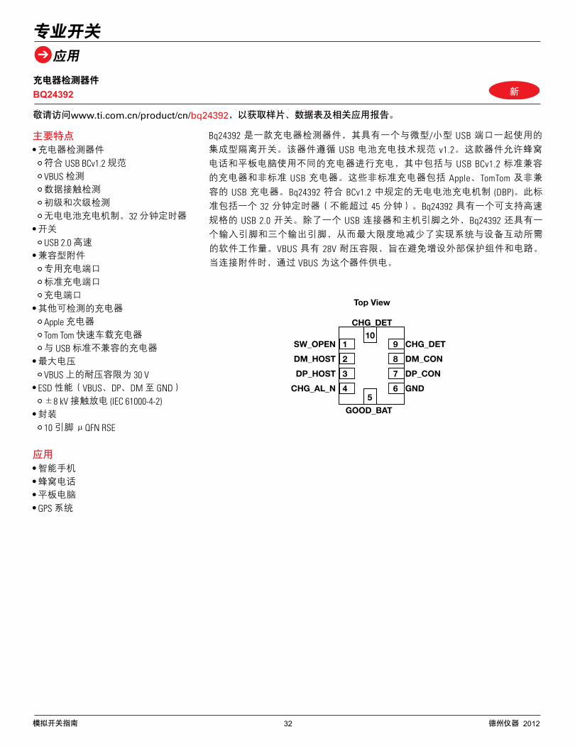
32Analog Switch Guide Texas Instruments 2012
Charger-Detection Device BQ24392
Get samples, data sheets and app reports at: www.ti.com/sc/device/BQ24392
Key Features
USB BCv1.2 compliant VBUS detection Data contact detection
Dead battery provision. 32 min timer
USB 2.0 high speed
Dedicated charging port Standard charging port Charging port
Apple charger Tom Tom charger Non-compliant USB charger
30V tolerance on VBUS
BUS, DP, DM to GND ± 8-KV contact discharge
(IEC 61000-4-2)
10-pin uQFN RSE
Applications
The BQ24392 is a charger-detection device with an integrated isolation switch for use with a micro/mini USB port. The device is compliant with USB battery charging specifi-
-ers including USB BCv1.2 compliant and non-standard USB chargers. These non-stan-
conforms to Dead Battery Provision (DBP) specified in BCv1.2. This includes a 32-min timer that cannot exceed 45 mins. This device has a USB 2.0 switch that supports high speed. In addition to USB connector and host pins, BQ24392 has one input and three output pins, resulting in minimum software workload for the system to interact with the device. VBUS has 28 V tolerance to avoid external protection. Power for this device is supplied via VBUS when accessory is attached.
Specialty Switches
Applications
1
2
3
4
9
8
7
65
10
Top View
CHG_DET
CHG_DET
DM_CON
DP_CON
GND
SW_OPEN
DM_HOST
DP_HOST
CHG_AL_N
GOOD_BAT
模拟开关指南 32 德州仪器 2012
充电器检测器件
BQ24392
专业开关
应用
主要特点 充电器检测器件
符合 USB BCv1.2 规范
VBUS 检测
数据接触检测
初级和次级检测
无电电池充电机制。32 分钟定时器
开关
USB 2.0 高速
兼容型附件
专用充电端口
标准充电端口
充电端口
其他可检测的充电器
Apple 充电器
Tom Tom 快速车载充电器
与 USB 标准不兼容的充电器
最大电压
VBUS 上的耐压容限为 30 V ESD 性能(VBUS、DP、DM 至 GND)
±8 kV 接触放电 (IEC 61000-4-2) 封装
10 引脚 μQFN RSE
应用 智能手机
蜂窝电话
平板电脑
GPS 系统
敬请访问www.ti.com.cn/product/cn/bq24392,以获取样片、数据表及相关应用报告。
Bq24392 是一款充电器检测器件,其具有一个与微型/小型 USB 端口一起使用的
集成型隔离开关。该器件遵循 USB 电池充电技术规范 v1.2。这款器件允许蜂窝
电话和平板电脑使用不同的充电器进行充电,其中包括与 USB BCv1.2 标准兼容
的充电器和非标准 USB 充电器。这些非标准充电器包括 Apple、TomTom 及非兼
容的 USB 充电器。Bq24392 符合 BCv1.2 中规定的无电电池充电机制 (DBP)。此标
准包括一个 32 分钟定时器(不能超过 45 分钟)。Bq24392 具有一个可支持高速
规格的 USB 2.0 开关。除了一个 USB 连接器和主机引脚之外,Bq24392 还具有一
个输入引脚和三个输出引脚,从而最大限度地减少了实现系统与设备互动所需
的软件工作量。VBUS 具有 28V 耐压容限,旨在避免增设外部保护组件和电路。
当连接附件时,通过 VBUS 为这个器件供电。
新
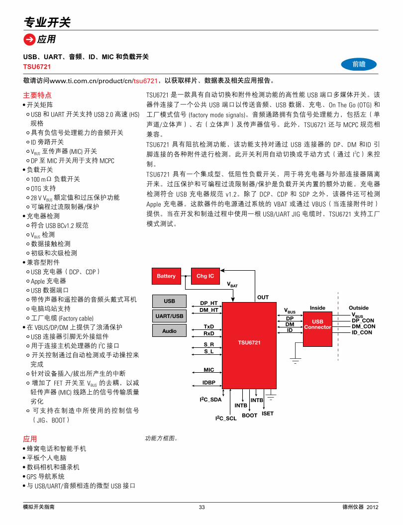
33Analog Switch Guide Texas Instruments 2012
USB, UART, AUDIO, ID, MIC, & Load Switch TSU6721
Get samples, data sheets and app reports at: www.ti.com/sc/device/tsu6721
Key Features
2.0 HS Audio switch with negative signal capability ID bypass switch VBUS to MIC switch DP to MIC switch to support MCPC
100 mΩ load switch OTG support 28V VBUS rating with over- voltage protection
Programmable overcurrent limiter/protection
USB BCDv1.2 compliant VBUS detection Data contact detection
Compatible accessories
Apple charger USB data port
Docking support Factory cable
BUS/DP/DM USB connector pins without external component I2C interface with host processor Switches controlled by automatic
detection or manual control Interrupts generated for
plug/unplug Decoupling FET switch to VBUS
added to reduce degradation on MIC line
Support control signals used In
Applications
AUDIO
TSU6721 is a high-performance USB port multimedia switch featuring automatic switching and accessory detection. The device connects a common USB port to pass audio, USB data, charging, On The Go (OTG) and factory mode signals. The audio path has negative signal capability includes left (mono/stereo), right (stereo) as well as micro-phone signals. Furthermore, TSU6721 is compatible with the MCPC specification.
TSU6721 features impedance detection which supports the detection of various acces-sories that are attached through DP, DM and ID pins of the USB connector. The switch is controlled by automatic switching or manually through I2C.
TSU6721 has an integrated, low-resistive, Load Switch that is used to isolate the charger from the external connector. Overvoltage protection and programmable over-current limiter/protection are additional features included to the load switch.The charger detection satisfies USB charger specification v1.2. In addition to DCP,
through VBAT of the system or through VBUS when attached. TSU6721 supports
manufacturing.
Specialty Switches
Applications
USB
VBUS
OUT
VBUS
VBAT
DP_CONDM_CONID_CON
Inside Outside
DPDMID
UART/USB
Audio
TSU6721
USBConnector
Battery Chg IC
S_RS_L
TxDRxD
DP_HTDM_HT
MIC
IDBP
I2C_SDA
I2C_SCL
INTB
BOOT
INTB
ISET
Functional block diagram.
模拟开关指南 33 德州仪器 2012
USB、UART、音频、ID、MIC 和负载开关
TSU6721
专业开关
应用
主要特点 开关矩阵
USB 和 UART 开关支持 USB 2.0 高速 (HS) 规格
具有负信号处理能力的音频开关
ID 旁路开关
VBUS 至传声器 (MIC) 开关
DP 至 MIC 开关用于支持 MCPC 负载开关
100 mΩ 负载开关
OTG 支持
28 V VBUS 额定值和过压保护功能
可编程过流限制器/保护
充电器检测
符合 USB BCv1.2 规范
VBUS 检测
数据接触检测
初级和次级检测
兼容型附件
USB 充电器(DCP、CDP) Apple 充电器
USB 数据端口
带传声器和遥控器的音频头戴式耳机
电脑坞站支持
工厂电缆 (Factory cable) 在 VBUS/DP/DM 上提供了浪涌保护
USB 连接器引脚无外接组件
用于连接主机处理器的 I2C 接口
开关控制通过自动检测或手动操控来完成
针对设备插入/拔出所产生的中断
增加了 FET 开关至 VBUS 的去耦,以减轻传声器 (MIC) 线路上的信号传输质量劣化
可支持在制造中所使用的控制信号(JIG、BOOT)
应用 蜂窝电话和智能手机
平板个人电脑
数码相机和摄录机
GPS 导航系统
与 USB/UART/音频相连的微型 USB 接口
敬请访问www.ti.com.cn/product/cn/tsu6721,以获取样片、数据表及相关应用报告。
TSU6721 是一款具有自动切换和附件检测功能的高性能 USB 端口多媒体开关。该
器件连接了一个公共 USB 端口以传送音频、USB 数据、充电、On The Go (OTG) 和工厂模式信号 (factory mode signals)。音频通路拥有负信号处理能力,包括左(单
声道/立体声)、右(立体声)及传声器信号。此外,TSU6721 还与 MCPC 规范相
兼容。
TSU6721 具有阻抗检测功能,该功能支持对通过 USB 连接器的 DP、DM 和ID 引脚连接的各种附件进行检测。此开关利用自动切换或手动方式(通过 I2C)来控
制。
TSU6721 具有一个集成型、低阻性负载开关,用于将充电器与外部连接器隔离
开来。过压保护和可编程过流限制器/保护是负载开关内置的额外功能。充电器
检测符合 USB 充电器规范 v1.2。除了 DCP、CDP 和 SDP 之外,该器件还可检测 Apple 充电器。这款器件的电源通过系统的 VBAT 或通过 VBUS(当连接附件时)
提供。当在开发和制造过程中使用一根 USB/UART JIG 电缆时,TSU6721 支持工厂
模式测试。
前瞻
功能方框图。
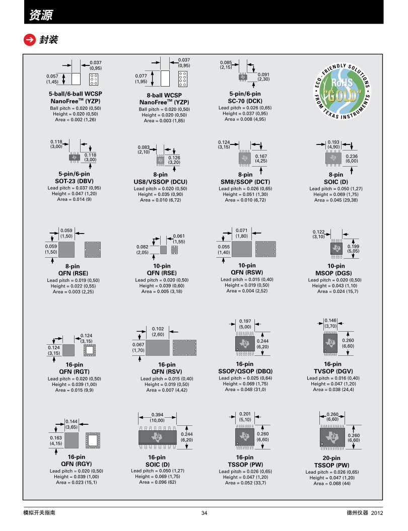
34Analog Switch Guide Texas Instruments 2012
0.037(0,95)
0.057(1,45)
Ball pitch = 0.020 (0,50)Height = 0.020 (0,50)Area = 0.002 (1,26)
5-ball/6-ball WCSPNanoFreeTM (YZP)
0.037(0,95)
0.077(1,95)
Ball pitch = 0.020 (0,50)Height = 0.020 (0,50)Area = 0.003 (1,85)
8-ball WCSPNanoFreeTM (YZP)
0.083(2,10)
0.126(3,20)
Lead pitch = 0.020 (0,50)Height = 0.035 (0,90)Area = 0.010 (6,72)
8-pinUS8/VSSOP (DCU)
0.061(1,55)
0.082(2,05)
Lead pitch = 0.020 (0,50)Height = 0.039 (0,60)Area = 0.005 (3,18)
10-pinQFN (RSE)
0.071(1,80)
0.055(1,40)
Lead pitch = 0.015 (0,40)Height = 0.019 (0,50)Area = 0.004 (2,52)
10-pinQFN (RSW)
0.122(3,10)
0.199(5,05)
Lead pitch = 0.020 (0,50)Height = 0.043 (1,10)
Area = 0.024 (15,7)
10-pinMSOP (DGS)
0.085(2,15)
0.091(2,30)
Lead pitch = 0.026 (0,65)Height = 0.037 (0,95)Area = 0.008 (4,95)
5-pin/6-pinSC-70 (DCK)
0.118(3,00)
0.118(3,00)
Lead pitch = 0.037 (0,95)Height = 0.047 (1,20)
Area = 0.014 (9)
5-pin/6-pinSOT-23 (DBV)
0.124(3,15)
0.167(4,25)
Lead pitch = 0.026 (0,65)Height = 0.051 (1,30)Area = 0.010 (6,72)
8-pinSM8/SSOP (DCT)
0.124(3,15)
0.124(3,15)
Lead pitch = 0.020 (0,50)Height = 0.039 (1,00)
Area = 0.015 (9,9)
16-pinQFN (RGT)
0.102(2,60)
0.067(1,70)
Lead pitch = 0.015 (0,40)Height = 0.019 (0,50)Area = 0.007 (4,42)
16-pinQFN (RSV)
0.197(5,00)
0.244(6,20)
Lead pitch = 0.025 (0,64)Height = 0.069 (1,75)Area = 0.048 (31,0)
16-pin SSOP/QSOP (DBQ)
0.146(3,70)
0.260(6,60)
Lead pitch = 0.016 (0,40)Height = 0.047 (1,20)Area = 0.038 (24,4)
16-pin TVSOP (DGV)
0.144(3,65)
0.163(4,15)
Lead pitch = 0.020 (0,50)Height = 0.039 (1,00)Area = 0.023 (15,1)
16-pinQFN (RGY)
0.394(10,00)
0.244(6,20)
Lead pitch = 0.050 (1,27)Height = 0.069 (1,75)
Area = 0.096 (62)
16-pin SOIC (D)
0.201(5,10)
0.260(6,60)
Lead pitch = 0.026 (0,65)Height = 0.047 (1,20)Area = 0.052 (33,7)
16-pin TSSOP (PW)
0.260(6,60)
0.260(6,60)
Lead pitch = 0.026 (0,65)Height = 0.047 (1,20)
Area = 0.068 (44)
20-pinTSSOP (PW)
0.059(1,50)
0.059(1,50)
Lead pitch = 0.019 (0,50)Height = 0.022 (0,55)Area = 0.003 (2,25)
8-pinQFN (RSE)
0.193(4,90)
0.236(6,00)
Lead pitch = 0.050 (1,27)Height = 0.069 (1,75)Area = 0.045 (29,38)
8-pinSOIC (D)
Resources
Packages
模拟开关指南 34 德州仪器 2012
资源
封装
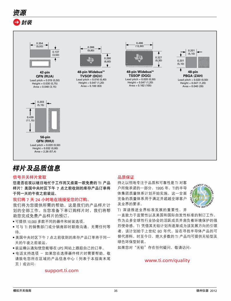
35Analog Switch Guide Texas Instruments 2012
Resources
Packages
0.354(9,00)
0.137(3,50)
Lead pitch = 0.019 (0,50)Height = 0.030 (0,75)Area = 0.048 (3,15)
42-pinQFN (RUA)
0.386(9,80)
0.260(6,60)
Lead pitch = 0.016 (0,40)Height = 0.047 (1,20)
Area = 0.100 (63)
48-pin WidebusTVSOP (DGV)
TM
0.203(5,15)
0.439(11,15)
Lead pitch = 0.020 (0,50)Height = 0.032 (0,80)
Area = 2.26 (57,4)
56-pinQFN (RHU)
0.201(5,10)
0.201(5,10)
Lead pitch = 0.020 (0,50)Height = 0.047 (1,20)
Area = 0.040 (26)
48-pinPBGA (ZAH)
0.496(12,60)
0.327(8,30)
Lead pitch = 0.020 (0,50)Height = 0.047 (1,20)Area = 0.162 (105)
48-pin WidebusTSSOP (DGG)
TM
Sample and Quality Information
Signal Switch Sample Requests
Working day and night and need a free TI product samplefast? Orders for material in stock received by 7 p.m. CST are shipped before midnight the same day.
We’re waiting to take your order on-line 24/7.
We’ll help you. That’s what our Product Sample program is all about. Helping you place your order for FREE product samples when you’re ready to place it.
shipped before midnight the same day.
the UPS Web site.
call your regional Product Information Center listed on the back page or visit
support.ti.com
Quality Assurance
elements of TI’s commitment to customers. In 1995, TI’s Semiconductor Group Quality System Program was launched. This
TI recognizes the importance of advancing industry stan-dards and is committed to working on regulatory as well as U.S. and international voluntary standards. As an active member of numer ous global industry associations and with a strong commitment to the environment, TI has emerged as a leader with its Lead (Pb)-Free programs. An initiative begun in the 1980s to find alternative materials for products has resulted in the majority of TI products now being available Pb-free and Green.
www.ti.com/quality
模拟开关指南 35 德州仪器 2012
资源
样片及品质信息
封装
信号开关样片索取您是否在夜以继日地忙于工作而又亟需一款免费的 TI 产品样片?美国中央时区下午 7 点之前收到的库存产品订单将于同一天的午夜之前装运。
我们将 7 天 24 小时地在线接受您的订购。我们将为您提供所需的帮助。这是我们的产品样片计划的全部工作。当您准备下单订购样片时,我们将帮助您完成免费产品样片的预订。 可提供 10,000 多款不同的器件和封装选项。
可与 TI 的销售部门或分销商即时联络沟通,无需任何等待。
美国中央时区下午 7 点之前收到的库存产品订单将于同一天的午夜之前装运。
装运确认通知使您能够在 UPS 网站上跟踪自己的订单。
电话支持选项 - 如果您在选择器件样片时需要帮助,敬请致电您所在区域的产品信息中心(列表于本指南末尾页)或访问:
support.ti.com
品质保证持之以恒地专注于品质和可靠性是 TI 对客户所做承诺的一部分。1995 年,TI的半导体集团质量体系计划开始实施。这一全面完备的质量体系用于满足并超越全球客户及业界的要求。
TI 深谙推进业界标准发展的重要性,并一直致力于监管性以及美国和国际自发性标准的制订工作。作为众多全球性行业协会的活跃成员并肩负着环境保护的强烈使命感,TI 凭借其无铅计划而逐渐成为该发展方向的引领者。该计划始于上世纪 80 年代,旨在寻找半导体产品的可替代原料,时至今日,绝大多数的 TI 产品均可提供无铅型及绿色环保型封装。
如果您对“无铅”存在任何疑问,敬请访问:
www.ti.com/quality
35Analog Switch Guide Texas Instruments 2012
Resources
Packages
0.354(9,00)
0.137(3,50)
Lead pitch = 0.019 (0,50)Height = 0.030 (0,75)Area = 0.048 (3,15)
42-pinQFN (RUA)
0.386(9,80)
0.260(6,60)
Lead pitch = 0.016 (0,40)Height = 0.047 (1,20)
Area = 0.100 (63)
48-pin WidebusTVSOP (DGV)
TM
0.203(5,15)
0.439(11,15)
Lead pitch = 0.020 (0,50)Height = 0.032 (0,80)
Area = 2.26 (57,4)
56-pinQFN (RHU)
0.201(5,10)
0.201(5,10)
Lead pitch = 0.020 (0,50)Height = 0.047 (1,20)
Area = 0.040 (26)
48-pinPBGA (ZAH)
0.496(12,60)
0.327(8,30)
Lead pitch = 0.020 (0,50)Height = 0.047 (1,20)Area = 0.162 (105)
48-pin WidebusTSSOP (DGG)
TM
Sample and Quality Information
Signal Switch Sample Requests
Working day and night and need a free TI product samplefast? Orders for material in stock received by 7 p.m. CST are shipped before midnight the same day.
We’re waiting to take your order on-line 24/7.
We’ll help you. That’s what our Product Sample program is all about. Helping you place your order for FREE product samples when you’re ready to place it.
shipped before midnight the same day.
the UPS Web site.
call your regional Product Information Center listed on the back page or visit
support.ti.com
Quality Assurance
elements of TI’s commitment to customers. In 1995, TI’s Semiconductor Group Quality System Program was launched. This
TI recognizes the importance of advancing industry stan-dards and is committed to working on regulatory as well as U.S. and international voluntary standards. As an active member of numer ous global industry associations and with a strong commitment to the environment, TI has emerged as a leader with its Lead (Pb)-Free programs. An initiative begun in the 1980s to find alternative materials for products has resulted in the majority of TI products now being available Pb-free and Green.
www.ti.com/quality
ZHCT041C
www.ti.com 原理图编辑器www.ti.com
1. Alternatively, it is availablesearch field to display a summary ofTINA-TI webpage.
released TINA-TI version are:98/ME/NT/2000/XP
SBOU052A–August 2007–Revised August 2008Submit Documentation Feedback
SBOU052A–2007年8月–2008年8月修订 TINA-TI™入门 11提交文档反
德州仪器在线技术支持社区 www.deyisupport.com
德州仪器 免费热线
重要声明
德州仪器(TI) 及其下属子公司有权在不事先通知的情况下, 随时对所提供的产品和服务进行更正、修改、增强、改进或其它更改,并有权随时中止提供任何产品和服务。客户在下订单前应获取最新的相关信息 , 并验证这些信息是否完整且是最新的。所有产品的销售都遵循在订单确认时所提供的TI 销售条款与条件。
TI 保证其所销售的硬件产品的性能符合TI 标准保修的适用规范。仅在TI 保证的范围内 , 且TI 认为有必要时才会使用测试或其它质量控制技术。除非政府做出了硬性规定 , 否则没有必要对每种产品的所有参数进行测试。
TI 对应用帮助或客户产品设计不承担任何义务。客户应对其使用TI 组件的产品和应用自行负责。为尽量减小与客户产品和应用相关的风险,客户应提供充分的设计与操作安全措施。
TI 不对任何TI 专利权、版权、屏蔽作品权或其它与使用了TI 产品或服务的组合设备、机器、流程相关的TI 知识产权中授予的直接或隐含权限作出任何保证或解释。TI 所发布的与第三方产品或服务有关的信息,不能构成从TI 获得使用这些产品或服务的许可、授权、或认可。使用此类信息可能需要获得第三方的专利权或其它知识产权方面的许可,或是TI 的专利权或其它知识产权方面的许可。
对于TI 的产品手册或数据表,仅在没有对内容进行任何篡改且带有相关授权、条件、限制和声明的情况下才允许进行复制。在复制信息的过程中对内容的篡改属于非法的、欺诈性商业行为。TI 对此类篡改过的文件不承担任何责任。
在转售TI 产品或服务时,如果存在对产品或服务参数的虚假陈述,则会失去相关TI 产品或服务的明示或暗示授权,且这是非法的、欺诈性商业行为。TI 对此类虚假陈述不承担任何责任。
TI 产品未获得用于关键的安全应用中的授权,例如生命支持应用(在该类应用中一旦TI 产品故障将预计造成重大的人员伤亡),除非各方官员已经达成了专门管控此类使用的协议。购买者的购买行为即表示,他们具备有关其应用安全以及规章衍生所需的所有专业技术和知识,并且认可和同意,尽管任何应用相关信息或支持仍可能由TI 提供,但他们将独力负责满足在关键安全应用中使用其产 品及TI产品所需的所有法律、法规和安全相关要求。此外,购买者必须全额赔偿因在此类关键安全应用中使用TI 产品而对TI 及其 代表造成的损失。
TI 产品并非设计或专门用于军事/航空应用,以及环境方面的产品,除非TI 特别注明该产品属于“军用”或“增强型塑料”产品。只 有TI指定的军用产品才满足军用规格。购买者认可并同意,对TI 未指定军用的产品进行军事方面的应用,风险由购买者单独承担,并且独力负责在此类相关使用中满足所有法律和法规要求。
TI 产品并非设计或专门用于汽车应用以及环境方面的产品,除非TI 特别注明该产品符合ISO/TS 16949 要求。购买者认可并同意,如果他们在汽车应用中使用任何未被指定的产品,TI 对未能满足应用所需要求不承担任何责任。
可访问以下URL 地址以获取有关其它TI 产品和应用解决方案的信息:
产品 应用
数字音频 www.ti.com.cn/audio 通信与电信 www.ti.com.cn/telecom
放大器和线性器件 www.ti.com.cn/amplifiers 计算机及周边 www.ti.com.cn/computer
数据转换器 www.ti.com.cn/dataconverters 消费电子 www.ti.com/consumer-apps
DLP® 产品 www.dlp.com 能源 www.ti.com/energy
DSP - 数字信号处理器 www.ti.com.cn/dsp 工业应用 www.ti.com.cn/industrial
时钟和计时器 www.ti.com.cn/clockandtimers 医疗电子 www.ti.com.cn/medical
接口 www.ti.com.cn/interface 安防应用 www.ti.com.cn/security
逻辑 www.ti.com.cn/logic 汽车电子 www.ti.com.cn/automotive
电源管理 www.ti.com.cn/power 视频和影像 www.ti.com.cn/video
微控制器 (MCU) www.ti.com.cn/microcontrollers
RFID 系统 www.ti.com.cn/rfidsys
OMAP 机动性处理器 www.ti.com/omap
无线连通性 www.ti.com.cn/wirelessconnectivity
德州仪器在线技术支持社区 www.deyisupport.com IMPORTANT NOTICE
邮寄地址: 上海市浦东新区世纪大道 1568 号,中建大厦 32 楼 邮政编码: 200122Copyright © 2012 德州仪器 半导体技术(上海)有限公司