distributed control and power quality improvement in
TRANSCRIPT

This document is downloaded from DR‑NTU (https://dr.ntu.edu.sg)Nanyang Technological University, Singapore.
Distributed control and power qualityimprovement in hybrid AC/DC microgrids
Jin, Chi
2013
Jin, C. (2013). Distributed control and power quality improvement in hybrid AC/DCmicrogrids. Doctoral thesis, Nanyang Technological University, Singapore.
https://hdl.handle.net/10356/61847
https://doi.org/10.32657/10356/61847
Downloaded on 26 Mar 2022 01:12:54 SGT

Distributed Control and Power
Quality Improvement in Hybrid
AC/DC Microgrids
Jin Chi
School of Electrical & Electronic Engineering
2013

Distributed Control and Power
Quality Improvement in Hybrid
AC/DC Microgrids
Jin Chi
School of Electrical & Electronic Engineering
A thesis submitted to the Nanyang Technological University
in partial fulfillment of the requirement for the degree of
Doctor of Philosophy
2013


i
Acknowledgements
This thesis and related research work would not have been possible without the
instruction and support of the following people.
First and foremost, I would like to express my sincere gratitude and appreciation to my
supervisor, Assoc. Prof. Dr. Peng WANG who was abundantly helpful and provided
invaluable assistance, support and guidance. The appreciation to Assoc. Prof. Dr. Peng
WANG is not limited to his valuable research guidance. I would also like to appreciate
his generous patience for my slower research progress due to my week background. In
addition, He always gave me sufficient latitude to explore ideas and new areas. Beyond
all that, I value the opportunities that he provided me to undertake a number of
non-thesis related projects which broadened my background and enriched my
professional experience.
Deepest gratitude is also due to the members of unofficial supervisory committee, Prof.
Dr. Poh Chiang LOH, Aalborg University, Denmark, and Prof. Dr. Yang MI, Shanghai
University of Electric Power, China. Without their knowledge sharing, guidance and
assistance, this study would not have been successful. Special thanks are given to Prof.
Dr. Poh Chiang LOH, who shared new research idea with me and taught me useful
simulation and experiment skills.
My acknowledgement is then extended to Prof. Dr. Frede BLAABJERG and Jesep M.
GUERRERO, Aalborg University, Denmark, for their valuable ideas and insightful
comments on my research works during my visiting in Aalborg University as an
exchange student. In particular, I would like to thank Professor Frede BLAABJERG for
financial support in exchange student duration.
In the laboratory, I am equally thankful to Mr. Thomos FOO, Ms. Chia-Nge Tak HONG
and Ms. Grace ONG from the Laboratory of Clean Energy Research, and Mr. Benny
CHIA and Miss Christina WONG from the Laboratory of Water Energy Research, for
their uncounted technical support in installations of academic software and setups of

ii
experimental prototype.
I would also like to express my love and gratitude to my beloved families for their
understanding and endless love through the duration of my studies. My parents have
inspired me throughout my life and have taught me never to give up. My wife who was
accompanying me in the last year of my PhD period has given me great support and
encouragement. Deepest gratitude is again given to my beloved families because of their
understanding and support during this period of struggle.
Last but not least, I would like to convey thanks to Nanyang Technological University
for providing the financial support and laboratory facilities.

iii
Table of Contents
ACKNOWLEDGEMENTS ............................................................................................. I
TABLE OF CONTENTS .............................................................................................. III
SUMMARY……………………………………………………………………………………. VII
LIST OF FIGURES ....................................................................................................... X
LIST OF TABLES ..................................................................................................... XIV
LIST OF ABBREVIATIONS...................................................................................... XV
CHAPTER 1 INTRODUCTION ................................................................................. 1
1.1. Background and Motivations ............................................................................ 1
1.2. Objectives ......................................................................................................... 3
1.3. Major Contributions .......................................................................................... 4
1.3.1. A hierarchical controlled DC microgrid ......................................................... 4
1.3.2. Global power sharing throughout a hybrid AC/DC microgrid ....................... 4
1.3.3. Distributed control for autonomous operation of a hybrid AC/DC/DS
microgrid ..................................................................................................................... 5
1.3.4. Hybrid AC/DC active power filter for power quality improvement in a hybrid
AC/DC microgrid ........................................................................................................ 5
1.4. Organization ...................................................................................................... 6
CHAPTER 2 CONCEPT OF HYBRID AC/DC MICROGRID .................................. 8
2.1. Introduction ....................................................................................................... 8
2.2. Review of Microgrids ....................................................................................... 9
2.2.1. Distributed generation ..................................................................................... 9
2.2.2. Microgrid systems ......................................................................................... 11
2.3. AC Microgrids versus DC Microgrids ............................................................ 12
2.3.1. Feasibility of AC microgrids ......................................................................... 12
2.3.2. Feasibility of DC microgrids ........................................................................ 13
2.4. Hybrid AC/DC Microgrids ............................................................................. 15
2.4.1. Why hybrid AC/DC microgrids? .................................................................. 15
2.4.2. An example of hybrid AC/DC microgrids structure ..................................... 18
2.4.3. Main advantages of hybrid AC/DC microgrids ............................................ 19

iv
2.5. Conclusions ..................................................................................................... 20
CHAPTER 3 HIERARCHICAL CONTROLLED DC MICROGRID ...................... 21
3.1. Introduction and Literature Review ................................................................ 21
3.2. System Configuration ..................................................................................... 23
3.3. Hierarchical Control ....................................................................................... 24
3.3.1. Hierarchical level I (HLI) control ................................................................. 26
3.3.2. Hierarchical level II (HLII) control .............................................................. 32
3.3.3. Hierarchical level III (HLIII) control ............................................................ 34
3.4. Modeling of System Elements ........................................................................ 35
3.4.1. Modeling of PV arrays .................................................................................. 35
3.4.2. Modeling of batteries .................................................................................... 36
3.4.3. Modeling of non-renewable source (NRS) ................................................... 36
3.5. Control Structures of Source/Storage Converters ........................................... 37
3.5.1. Control of modular PV DC/DC converters ................................................... 38
3.5.2. Control of bidirectional DC/DC battery converters ...................................... 42
3.5.3. Control of non-renewable source (NRS) converters ..................................... 45
3.6. Hardware Implementation for Verifications ................................................... 45
3.6.1. Prototype of a lab-scale DC microgrid ......................................................... 45
3.6.2. Experimental results ...................................................................................... 47
3.7. Conclusions ..................................................................................................... 51
CHAPTER 4 GLOBAL POWER SHARING (GPS) CONTROL FOR
AUTONOMOUS OPERATION OF HYBRID AC-DC MICROGRIDS ..................... 52
4.1. Introduction ..................................................................................................... 52
4.2. System Configuration ..................................................................................... 53
4.3. Power Sharing in Individual AC or DC Microgrid ......................................... 55
4.3.1. Review of rudimentary droop control ........................................................... 55
4.3.2. Review of improved variants of droop control ............................................. 60
4.3.3. Power sharing in AC microgrids ................................................................... 64
4.3.4. Power sharing in DC microgrids ................................................................... 66
4.4. Global Power Sharing throughout a Hybrid AC/DC Microgrid ..................... 70
4.4.1. Principle of global power sharing ................................................................. 70
4.4.2. Control structure of interlinking converter ................................................... 77
4.5. Simulation Results .......................................................................................... 78
4.6. Experiment Verifications ................................................................................ 82
4.7. Conclusions ..................................................................................................... 87
v
CHAPTER 5 DISTRIBUTED CONTROL FOR AUTONOMOUS OPERATION OF
HYBRID AC/DC/DS MICROGRIDS .......................................................................... 88
5.1. Introduction ..................................................................................................... 88
5.2. Proposed Hybrid AC/DC/DS Structure .......................................................... 88
5.3. Proposed Distributed Control ......................................................................... 91
5.4. Storage Power Sharing for DS Units .............................................................. 93
5.5. Multi-level Power Exchange Control ............................................................. 97
5.5.1. Scheduling of global power sharing (GPS) operation .................................. 98
5.5.2. Scheduling of storage power sharing (SPS) operation ................................. 99
5.6. Simulation Results ........................................................................................ 100
5.7. Experiment Verifications .............................................................................. 104
5.8. Conclusions ................................................................................................... 109
CHAPTER 6 HYBRID AC/DC ACTIVE POWER FILTERS (HAPF) FOR POWER
QUALITY IMPROVEMENT IN HYBRID AC/DC MICROGRID .......................... 110
6.1. Introduction ................................................................................................... 110
6.2. Three-Phase Three-Wire Shunt Active Power Filter (APF) in AC Microgrid ....
...................................................................................................................... 111
6.2.1. Review of active power filters (APFs) ........................................................ 111
6.2.2. A Common problem for shunt active power filters (SAPFs) ...................... 113
6.2.3. Required DC-link capacitance for SAPFs .................................................. 114
6.3. DC Active Power Filter — DC-link Compensator (DLC) ........................... 117
6.3.1. Principle of DC-link compensator (DLC) ................................................... 117
6.3.2. Design of DC-link compensator (DLC) ...................................................... 120
6.4. Control of Active Power Filter (APF) and DC-link Compensator (DLC)….121
6.4.1. Control of active power filter (APF) ........................................................... 121
6.4.2. Control of DC-link compensator (DLC) ..................................................... 123
6.5. Simulation Results ........................................................................................ 125
6.6. Prototype Setup and Experiment Verifications ............................................. 126
6.6.1. Description of proposed hybrid AC/DC power filter prototype ................. 126
6.6.2. Experiment Results ..................................................................................... 128
6.7. Conclusions ................................................................................................... 131
CHAPTER 7 CONCLUSIONS AND RECOMMENDATIONS ............................. 133
7.1. Conclusions ................................................................................................... 133

vi
7.2. Recommendations ......................................................................................... 136
AUTHOR’S PUBLICATIONS ................................................................................... 138
BIBLIOGRAPHY ....................................................................................................... 140
vii
Summary
Global concerns on fossil fuel depletion and environmental pollution have initiated an
increasing demand for renewable energy such as solar, wind and fuel cells etc. More
distributed generations (DGs) powered by renewable energy sources (RESs) will be
entering into the existing electricity network in the near future. Clustering a few DGs,
loads and storages together forms entities known as microgrids which merge advantages
of individual DG units to arrive at an operating efficiency and system reliability that can
never be attained by any single DG. Realization of those advantages accompanies the
development of various essential power conditioning interfaces and their associated
control for tying multiple DGs to the microgrids, and then tying the microgrids to the
traditional power systems. Moreover, the intermittent characteristics of most green
sources like photovoltaic (PV) arrays, wind turbines (WT) strongly rely on climatic or
environmental condition, which makes RES uncontrollable. To overcome those inherent
deficiencies, power electronics is the key enabling technology for the interconnection
between RESs and the utility grid, providing more control flexibilities so as to fulfill
system reliability and power quality requirements.
The proliferation of popular RESs like PV and fuel cells, and energy storages (ESs) like
batteries and ultra-capacitors, which are all DC by nature, facilitates widespread
application of DC microgrid in many industry systems, commercial buildings and
residential complex. The advantages of DC microgrids include better compatibility,
higher efficiency and robust stability. To cope with the stochastic nature of RESs, stable
operation of a standalone DC microgrid with multiple DC sources, ESs and loads
invariably involves the development of flexible and reliable control strategies for power
balancing in both power generation and consumption ends. A coordination control
scheme among multiple DC sources and ESs interfaces is implemented using a novel
hierarchical control technique to maintain DC bus voltage within the limits while
harvesting maximum renewable energy and prolonging storage lifetime.
Combining the DC microgrid and the dominated AC system forms the scenario —
hybrid AC/DC microgrid, which would be, in concept, the presence of both DC and AC
microgrids with sources, storages, loads and appropriate interlinking converters (ICs)

viii
tied between them. Hybrid AC/DC microgrid has been becoming a popular concept to
provide an effective solution for unlimited large-scale integration of various DGs and
distributed storages (DSs) because of its higher efficiency and better compatibility.
Normal operations of hybrid system include local energy management within each
sub-grid and power exchange tuning between two sub-grids, which usually involve
multi-layer supervision system and advanced energy management algorithm with vast
communication links. However, it is impractical to linkup widely dispersed DGs
through communication wirings. This would undoubtedly degrade system redundancy.
The challenge is thus to avoid the wiring by developing appropriate decentralized
control. With this in mind, a global power sharing (GPS) control is proposed to manage
local power sharing (LPS) in individual sub-grid and GPS throughout the entire hybrid
system.
Due to the load variations at the demand end and the intermittent renewable power at
the supply end, the hybrid AC/DC microgrid can hardly be fully autonomous unless the
DSs are placed for energy buffering, power balancing and fault riding-through. The
storages, such as batteries, ultra-capacitors, flywheels etc., can be configured to behave
in different manners according to specific microgrid applications and their respective
features. Storages with high energy like batteries are usually placed for long-term
system operation, serving as a controlled current source. While the high power storages
like ultra-capacitors are usually controlled as a voltage source, maintaining system
power balance in transient state. In this sense, different control schemes for DSs would
undoubtedly increase the complexity of power management in hybrid AC/DC microgrid
in spite of DS locations in AC or DC microgrid. Therefore, fulfilling the requirement of
“plug-and-play” is getting difficult since all DSs are not controlled in a coincident way.
To avoid the complexity of power management and enforce a coincident control scheme
to DSs, a hybrid microgrid scenario with three buses including AC, DC, and DS buses is
proposed. LPS in individual sub-grid, GPS throughout entire hybrid system and storage
power sharing (SPS) among DS units are well elaborated. To restrain unexpected GPS
behaviors and reduce the usage of DSs, a multi-level power exchange control strategy is
developed to schedule the activation sequences among LPS, GPS and SPS.
The interlinking converter between AC and DC microgrids can be used not only to
manage fundamental power flow among two sub-grids but also to serve as an active
ix
power filter (APF), drawing harmonic current from AC to DC microgrid so as to
improve the power quality in AC sub-grid. The ripple power injected into the DC
microgrid results in voltage ripple in DC bus voltage, which is harmful for stable
operation of DC system. A DC-link compensator (DLC) is therefore developed to sink
the harmonic power, transferring it to auxiliary DLC. In this way, the variation of the
DC bus voltage can be limited within an accepted band even with a relative smaller
DC-link capacitance.
The hierarchical control scheme for standalone DC microgrids, the fully decentralized
control for hybrid AC/DC microgrids, the distributed control for hybrid AC/DC/DS
microgrids and power quality improvement for hybrid AC/DC microgrid have been
verified in theory, simulation and experiment, and will definitely facilitate the
application and development of hybrid AC/DC microgrid in low voltage distribution
systems.

x
List of Figures
Figure 2.1. Basic AC microgrid structure. ...................................................................... 13
Figure 2.2. Basic DC microgrid structure. ...................................................................... 15
Figure 2.3. A hybrid AC/DC microgrid at the WERL, NTU. ............................................ 19
Figure 3.1. Configuration of DC microgrid. ................................................................... 24
Figure 3.2. I-V characteristic of DC bus voltage under HLI control. .............................. 26
Figure 3.3. Batteries droop characteristic. .................................................................... 27
Figure 3.4. BESS charging scheme. ................................................................................ 28
Figure 3.5. Illustration of impact of PV generations reduction on DC bus characteristics:
(a). the drawback of HLI control; (b). the improvement in HLII control. .. 30
Figure 3.6. Impact of BESS charging capability reduction: (a). the drawback of HLI
control; (b). the improvement in HLII control. .......................................... 31
Figure 3.7. PV modeling: (a). equivalent circuit of a solar cell, (b). symbol of PV arrays.
................................................................................................................... 35
Figure 3.8. I-V and P-V characteristics of PV arrays. ..................................................... 36
Figure 3.9. (a). Non-Linear battery model, (b). symbol of battery tanks. ..................... 37
Figure 3.10. Symbol of NRS. .......................................................................................... 37
Figure 3.11. Equivalent circuit of the operation of PV arrays. ...................................... 38
Figure 3.12. Illustration of different operation points for PV arrays. ............................ 39
Figure 3.13. Common PV system with the feature of MPPT. ........................................ 39
Figure 3.14. Flowchart of P & O algorithm. .................................................................. 40
Figure 3.15. BM control for PV modules. ...................................................................... 41
Figure 3.16. Mode selection and control diagram of PV modules. .............................. 42
Figure 3.17. Bidirectional DC/DC battery converter. ..................................................... 42
Figure 3.18. Battery converter in charge/discharge state: (a). boost converter in
discharge state; (b). buck converter in charge state. ................................ 43
Figure 3.19. BM control for BESS. ................................................................................. 43
Figure 3.20. Block diagram of CC and CV controls during BESS charging stage. ........... 44
Figure 3.21. Mode selection and control diagram of BESS units. ................................. 45

xi
Figure 3.22. Mode selection and control diagram of NRS units. .................................. 45
Figure 3.23. Configuration of a scale-down DC grid. .................................................... 46
Figure 3.24. Lab scale implementations for experimental testing. ............................... 46
Figure 3.25. Current and power outputs of PV modules, BESS and bus voltage during
mode transfer from Region 1 to Region 3. ................................................ 47
Figure 3.26. Current and power outputs of BESS and bus voltage during mode transfer
between Region 2 and Region 3. .............................................................. 49
Figure 3.27. Transient performances of battery converter from BM mode to CCC mode.
................................................................................................................... 50
Figure 3.28. Experimental illustration when dc microgrid is controlled from HLII to HLI
during communication failure. .................................................................. 50
Figure 4.1. Layout of an example hybrid AC-DC microgrid. .......................................... 54
Figure 4.2. The example hybrid AC-DC microgrid with detailed system components. . 54
Figure 4.3. Equivalent circuit of a voltage controlled PWM inverter connected to a
common AC bus. ....................................................................................... 56
Figure 4.4. Droop control functions for (a) inductive output impedance and (b)
resistive output impedance. ..................................................................... 59
Figure 4.5. Block diagram of the rudimentary droop control method. ........................ 60
Figure 4.6. Block diagram of the closed-loop VSI with the virtual output impedance
path. .......................................................................................................... 61
Figure 4.7. Block diagram of improved droop control with power derivative and
integral terms for enhancing system transient stability. ........................... 63
Figure 4.8. Block diagram of droop control with distorted power sharing. .................. 64
Figure 4.9. Droop characteristics for DGs in AC sub-grid. ............................................. 65
Figure 4.10. Control scheme for AC micro-sources DG3 and DG4. ............................... 66
Figure 4.11. Droop characteristics of DGs in DC sub-grid: (a) basic droop; (b) modified
droop. ........................................................................................................ 68
Figure 4.12. Equivalent circuit of a two-source DC microgrid. ..................................... 68
Figure 4.13. Simulation verifications of modified droop characteristics for DG units in a
two-source DC microgrid. ......................................................................... 69
Figure 4.14. Control scheme for DGs in DC sub-grid. ................................................... 70
Figure 4.15. Combined AC droop characteristics. ......................................................... 72

xii
Figure 4.16. Combined DC droop characteristics. ......................................................... 72
Figure 4.17. Combined normalized droop droop characteristics of (a). AC sub-grid; (b).
DC sub-grid. ............................................................................................... 74
Figure 4.18. Global power sharing realization. ............................................................. 74
Figure 4.19. Illustration of GPS principle: (a) & (b) individual droop characteristics; (c)
& (d) combined droop characteristics; (e) & (f) normalized combined
droop characteristics; (g) GPS realization. ................................................ 75
Figure 4.20. Control block diagram of interfacing converter. ....................................... 77
Figure 4.21. Test bed of hybrid AC/DC microgrid for global power sharing verifications
in both simulation and experiment. ......................................................... 78
Figure 4.22. Simulation results of the GPS controlled hybrid microgrid. ..................... 79
Figure 4.23. Experimental AC and DC waveforms in transient event 1: (a) output
power of AC source; (b) AC system frequency; (c) AC load; (d) DC source
output, DC load and power flow on interlinking converter. ..................... 84
Figure 4.24. Experimental AC and DC waveforms in transient event 2: (a) output
power of AC source; (b) AC system frequency; (c) AC load; (d) DC source
output, DC load and power flow on interlinking converter. ..................... 86
Figure 5.1. Overview of the architecture of hybrid AC/DC/DS microgrid. .................... 89
Figure 5.2. System configuration of the proposed hybrid AC/DC/DS microgrid. .......... 90
Figure 5.3. Circuit diagrams of: (a) DG unit in AC network; (b) DG unit in DC network;
(c) DS unit in DS network; (d) two-stage interlinking converter (IC)
interconnecting AC and DC networks. ...................................................... 90
Figure 5.4. Illustration of the proposed distributed control for hybrid AC/DC/DS
microgrid. .................................................................................................. 92
Figure 5.5. Capacity-based demand droop for SPS among DSs in DS network. ........... 94
Figure 5.6. Illustration of SoC-based demand droop control on managing SPS during (a)
charging mode; (b) discharging mode. ..................................................... 96
Figure 5.7. Illustration of multi-level power exchange control. .................................... 98
Figure 5.8. Conditions and associated mode switching of LPS, GPS, and SPS. ........... 100
Figure 5.9. Test bed of the proposed hybrid AC/DC/DS system. ................................ 101
Figure 5.10. Simulated active power flows on source, storage and interlinking
converters. .............................................................................................. 102

xiii
Figure 5.11. Transients from LPS to LPS+GPS: (a) AC source output power; (b) AC
frequency; (c) AC load; (d) profiles of DC network and IC2. ................... 106
Figure 5.12. Transients from LPS+GPS to LPS+GPS+SPS: (a) AC source output power; (b)
AC bus frequency; (c) AC load; (d) DC network profiles and power flow on
IC1; (e) power flow on IC2; (f) power flow on DS1 and DS2. .................. 108
Figure 6.1. Principle of shunt current compensator. .................................................. 111
Figure 6.2. A typical three-phase three-wire shunt APF system. ................................ 115
Figure 6.3. The proposed hybrid AC/DC active power filter including a conventional
three-phase three-wire SAPF and a DLC. ................................................ 117
Figure 6.4. Idealized operating waveforms for four-quadrant (b) (c) and two-quadrant
(d) (e) DC-link compensators. ................................................................. 119
Figure 6.5. Control block diagram of APF. ................................................................... 122
Figure 6.6. Control block diagram of DLC stage. ......................................................... 124
Figure 6.7. Logic operator for activation of DLC stage. ............................................... 125
Figure 6.8. Simulated results showing the effectiveness of the proposed DLC concept.
................................................................................................................. 126
Figure 6.9. Experimental setup of the APF system with a DLC. .................................. 127
Figure 6.10. Experimental results of steady state performance of APF system with a
33μF dc-link capacitance. ........................................................................ 128
Figure 6.11. Harmonic current spectrum: APF versus APF with a DLC. ...................... 129
Figure 6.12. Experimental results of steady state performance of: (a) APF system; (b)
dc-link compensator. ............................................................................... 129
Figure 6.13. Experimental results of proposed APF system with a DLC when subjected
to a 100% to 50% step-down load change. ............................................. 131

xiv
List of Tables
Table 2.1. Some typical loads in future power systems. ............................................... 16
Table 2.2. Power conversion flow for different sources and loads in AC and DC
microgrids. ................................................................................................ 18
Table 3.1. Voltage thresholds for hierarchical controlled DC microgrids. .................... 25
Table 3.2. Illustration of SoC-based droop coefficient. ................................................ 33
Table 3.3. Mode Selection for PV, BESS and NRS Converters. ................................... 38
Table 4.1. Output impedance impacts over power flow controllability. ....................... 59
Table 4.2. Parameters of two-source DC Microgrid. .................................................... 69
Table 4.3. System parameters for both simulation and experiment. ............................. 79
Table 4.4. Power flows of system components for different scenarios in simulation. .. 81
Table 4.5. Power flows of system components for different scenarios in experiment.. 87
Table 5.1. System Parameters for Simulation and Experiment Verifications. ............ 101
Table 6.1. System Parameters used for Simulation. .................................................... 121
Table 6.2. System parameters used for scale-down laboratory experiments. ............. 127
Table 6.3. Harmonic content in the DC-link voltage. ................................................. 128

xv
List of Abbreviations
AC Alternative Current
ACwC AC loads with Converter
APF Active Power Filter
BESS Battery Energy Storage System
BM Bus Monitoring
CCC Constant-Current Charging
CC-CV Constant Current and Constant Voltage
CERTS Consortium for Electric Reliability Technology Solutions
CPL Constant Power Load
CSI Current Source Inverter
CV Constant Voltage
CVC Constant-Voltage Charging
DAC Digital-Analog Converter
DBS DC Bus Signaling
DC Direct Current
DER Distributed Energy Source
DG Distributed Generation
DLC DC-Link Compensator
DS Distributed Storage
DVD Digital Video Disk
EMF Electromotive Force
EMS Energy Management System
ES Energy Storage
ESR Equivalent Series Resistant
ESS Energy Storage System
EV Electric Vehicle
GPS Global Power Sharing
HL I Hierarchical level I
HL II Hierarchical level II
HL III Hierarchical level III
HVDC High Voltage Direct Current

xvi
IC Interlinking Converter
ICC Interrupted Charge Control
INC Incremental Conductance
LED Light-Emitting Diode
LPS Local Power Sharing
MPP Maximum Power Point
MPPT Maximum Power Point Tracking
MTBF Mean Time Between Failures
NRS Non-Renewable Source
NTU Nanyang Technological University
PCC Point of Common Coupling
PI Proportional-Integral
PLL Phase Lock Loop
P&O Perturb and Observe
PEV Plug-in Electric Vehicle
PR Proportional-Resonant
PV Photovoltaic
RES Renewable Energy Source
RMS Root Mean Square
SoC State of Charge
SPS Storage Power Sharing
THD Total Harmonic Distortion
VCO Voltage Controlled Oscillator
VSD Variable Speed Drives
VSI Voltage Source Inverter
WERL Water and Energy Research Laboratory
WT Wind Turbines

1
Chapter 1 Introduction
1.1. Background and Motivations
During the last two decades, distributed generations (DGs), powered by various
renewable and nonconventional micro-sources, have been gradually becoming an
attractive option for configuring modern or future electrical grids because of the
advantages of environmental friendliness, expandability and flexibility [1]. When a few
DGs and loads are further clustered together, entities known as microgrids are formed,
which in concept, are larger controllable distributed generators that effectively merge
the advantages of various nonconventional sources to arrive at an operating efficiency
and system reliability that can never be attained by any single micro-source [2, 3].
Accompanying this advancement in DG and microgrids is the development of various
essential power conditioning interfaces and their associated control for tying the DGs
in a microgrid, and between the microgrids and the traditional power systems [4, 5].
With such interconnection, the renewable energy sources with intermittent
characteristics, such as photovoltaic (PV), wind and fuel cells, can be connected to the
utility with stable operations under proper control scheme. Moreover, the microgrid
operation is highly flexible, allowing it to freely operate in the grid-connected or
islanded mode of operation [6-8].
So far, the applications of AC microgrids have been widely spread because of its main
advantage of compatibility with the existing AC system infrastructure. This is
understandable based on the dominant role that AC distribution has long served in the
traditional grid. Although not rapidly developed, the applications of DC microgrid can
also be found more than a decade back [9, 10], but its popularity has not grown much
then, until the recent decade when the researches and applications of renewable energy
have been rapidly developed [11-13]. Nowadays, the popularity of DC microgrids are
growing further due to the proliferation of popular “green sources” like PV and fuel
cells, and energy storages (ESs) like batteries and ultra-capacitors, which are all DC by
nature. Given also that a huge portion of modern loads are electronic circuits that need

2
DC rather than AC supply, forming of DC microgrids might indeed be more efficient
since less power conversion stages are required [14].
Being convinced of respective features of AC and DC microgrids, the natural idea is to
form a more likely scenario — hybrid AC/DC microgrid, which would be the
coexistence of both AC and DC microgrids with sources, storages and loads
appropriately organized between them [12]. The two microgrids can then be tied
together by proper interfacing converters, which preferably should be simple like the
traditional six-switch half-bridge AC/DC converter with mature control schemes and
proved stable performances in order to avoid unnecessary complexity and cost. This
hybrid AC/DC microgrid can therefore provide an effective solution for integration of
unlimited DGs, distributed storages (DSs) and various AC/DC loads with higher
efficiency and better compatibility.
In general, reliable and economical operations of such a complex hybrid AC/DC
microgrid usually depend heavily on local controllers for basic operations of power
conditioning interfaces in the low layer and advanced energy management system
(EMS) with mass information exchange in the high layer for overall system
optimization. However, this kind of centralized control scheme may suffer degraded
system redundancy during the malfunction of communication carriers [15]. What if the
failures in communication networks occur? Is it possible to ride-through the
communication failures? Or is there a solution for maintaining reliable operations
without communication networks which can hardly be afforded and built up in the
rural and remote areas?
With the above concerns in mind, the challenge is then to decentralize the control for
DC sources, AC sources and interfacing converter so that the power flow is always
appropriately managed within each microgrid as well as throughout the whole hybrid
microgrid regardless of whether the load change happens in the AC, DC or both
microgrids. Considering the power exchange between two microgrids, fully
decentralized control however cannot be as straightforward as the decentralized control
simply applied to DGs in single microgrid since power information in both microgrids
cannot be easily gathered in a decentralized manner. Because of that, a rule of power
3
exchange between AC and DC microgrids under fully decentralized control needs to be
developed. Although fully decentralized control gives the answer to the solution of
previous concerns, system with decentralized control is however lack of optimal
fashion since each power module is unaware of the others [16]. The follow-up thought
is to explore an improved control strategy which is capable of not only managing the
overall system power flow in decentralized manner, but also increasing the system
optimal fashion to a certain degree. This challenge is therefore the core motivation of
this research work.
1.2. Objectives
The focus of this Ph.D research work is the development of control schemes for
reliable operations and power quality improvement of hybrid AC/DC microgrids. The
main objectives of this research work are briefly summarized as:
To discuss the feasibility of AC and DC microgrids and make a comparison
between two types of microgrids in terms of economical, technical and
environmental benefits of renewable based DGs.
To give an overview of significant research on the efficiency advantages of DC
distribution system over AC.
To illustrate the infrastructure of hybrid AC/DC microgrids and address the
accompanied advantages of combination of AC and DC microgrids.
To give a comprehensive review of existing control schemes for wireless power
sharing in distributed systems.
To build up a practical DC microgrid in laboratory and develop associated
control strategy for proper operations with respect to maximum energy harvest,
effective battery management and utilization priority of renewable energy.
4
To expand independent power sharing control in individual AC or DC
microgrid to the hybrid system and develop a broadened wireless power
sharing method throughout entire hybrid AC/DC microgrid.
To develop a distributed control strategy for coordination operations between
DGs and distributed storages in hybrid microgrids system.
To investigate on the harmonic suppression in hybrid AC/DC microgrids and
attempt to explore effective solutions [17].
To extend the concept of active power filter in AC microgrids to DC microgrids
and solve out the hybrid AC/DC active power filters.
1.3. Major Contributions
The main contributions of this research work can be summarized as follows:
1.3.1. A hierarchical controlled DC microgrid
A practical DC microgrid is developed in Water and Energy Research Laboratory
(WERL) in Nanyang University of Technology, Singapore. The coordination control
among multiple DC sources and ESs is implemented using a novel hierarchical control
technique. The bus voltage essentially acts as an indicator of supply-demand balance.
A wireless control is implemented for reliable operation of the grid. A reasonable
compromise between maximum power harvest and effective battery management is
further enhanced using coordination control based on a central EMS. The feasibility
and effectiveness of the proposed control strategies have been eventually tested by a
DC microgrid in WERL.
1.3.2. Global power sharing throughout a hybrid AC/DC microgrid
Power sharing issues of an autonomous hybrid microgrid have been investigated. The
hybrid microgrid comprises DC and AC subgrids interconnected by power electronic
interfaces. A global power sharing (GPS) control is developed to manage power flows
among all sources distributed throughout the two types of subgrids, which is certainly

5
tougher than pre-existing power sharing methods developed for individual AC or DC
microgrid. This broadened power sharing control relies on coordinated operation of
DC sources, AC sources, and interlinking converters (IC), scheduling all sources to
share the total load throughout the entire hybrid AC/DC microgrid. The proposed
method has been verified in simulation and experimental tests. The hybrid microgrid
concepts are likely to benefit renewable or nonconventional distributed generations
(DGs), where both AC and DC sources are present.
1.3.3. Distributed control for autonomous operation of a hybrid
AC/DC/DS microgrid
The hybrid system can hardly be fully autonomous if distributed storages (DSs) are not
considered. Storages can be placed for energy buffering, power balancing and fault
riding-through. A hybrid AC/DC/DS microgrid configuration is proposed based on the
layout of hybrid AC/DC system. In this three-bus system, sources and storages with
same type are placed together in the relevant bus. Storages with the coincident control
scheme would beneficially reduce the complexities in coordination control among
three buses. The wireless power management of such a complex AC/DC/DS system
would certainly rely on the development of a distributed control strategy, which
manages the power flow within each network and tunes the power exchanges amongst
three networks. The proposed distributed control strategy for three-bus AC/DC/DS
hybrid system has subsequently been verified in both simulation and laboratory-scale
experimental results.
1.3.4. Hybrid AC/DC active power filter for power quality improvement
in a hybrid AC/DC microgrid
In a hybrid AC/DC microgrid system, the ICs interconnecting AC and DC microgrids
can also operate as shunt active power filters (APF) to buffer harmonic power
generated from the AC side. The shunt APF usually employs very large electrolytic
capacitors in DC bus to maintain relatively constant DC bus voltage. These capacitors
are however known to be bulky, suffering from expensive cost and short lifetime. A
DC-link compensator (DLC) is developed to eliminate harmonic power in DC bus and
very small electrolytic capacitors or even film type capacitors can be used instead. The
DC side power quality can therefore be improved with proper design of DLC which is

6
constructed with small passive components and features very simple circuit
configuration. Finally, simulation and experimental results are provided to prove that
the proposed DLC concept can be a very promising harmonic solution for industrial
applications of APFs.
1.4. Organization
This thesis is composed of seven chapters including this introductory chapter. The
following six chapters are arranged as follows:
Chapter 2 introduces the concept of hybrid AC/DC microgrid as well as its main
advantages. After a brief review of DGs and microgrids, the feasibility of AC and DC
microgrids are compared. An example of hybrid AC-DC microgrids structure is then
described in order to address the potential aims of a test bed hybrid microgrid. Finally,
the main advantages of proposed hybrid AC/DC microgrid have been summarized.
Chapter 3 presents the implementation of a hierarchical control scheme for reliable
operation of a standalone PV/battery based DC microgrid. The layout of a standalone
DC microgrid is first described. The proposed hierarchical control applied to the DC
system is then analyzed. Control structures of each power module for different modes
of operations are subsequently obtained. Finally, the effectiveness of the proposed
hierarchical control scheme has been experimentally verified through a lab-scale DC
microgrid.
Chapter 4 proposes a GPS control for active power sharing of an autonomous hybrid
AC/DC microgrid. The hybrid AC/DC structure is first introduced. The rudimentary
droop control and its improved variants are reviewed. The power sharing in individual
AC and DC sub-grid are then described. Upon accurate power sharing in both sub-grids,
the principle of GPS is elaborated with the help of mathematical and graphical
explanations. Finally, the simulation and experiment results have been provided to
prove the effectiveness of the proposed control scheme for active power sharing of an
autonomous hybrid AC/DC microgrid.
Chapter 5 proposes a distributed control for autonomous operation of hybrid

7
AC/DC/DS microgrid. The infrastructure of a three-bus hybrid AC/DC/DS microgrid
is first described. To maintain reliable operation and achieve improved optimal degree,
a distributed control scheme including a fully decentralized control for reliable
operation of overall hybrid system and a multi-level power exchange control for
optimal degree improvement is then introduced. Finally, simulation and experiment
results are provided to show the effectiveness of the proposed distributed control
stragety.
Chapter 6 proposes hybrid AC/DC active power filters which includes a conventional
three-phase three-wire shunt APF for harmonic attenuation in AC microgrid and an
active DC power filter — DLC for harmonic power decoupling in DC-link. In this
chapter, the principle of shunt APF is first reviewed and a common problem inherent in
the existing shunt APF applications is addressed. To illustrate this common
accompanied problem, the minimum requirement of DC-link capacitance for
three-phase three-wire shunt APF is then analyzed. In order to resolve the issues
caused by the common inherent problem of shunt APF, the concept of DLC and its
operation principle are subsequently explained. To verify the effectiveness of proposed
hybrid AC/DC APF, comprehensive simulation and experimental results have been
finally carried out.
Finally, Chapter 7 concludes this research work and proposes future research work
based on the achievements of this work.
8
Chapter 2 Concept of Hybrid AC/DC Microgrid
2.1. Introduction
Alternative current (AC) has been the dominant power supply medium for over a
century since the end of “the war of currents” [18] in which Thomas Edison and
George Westinghouse became adversaries due to Edison’s promotion of direct current
(DC) for electric power distribution over AC advocated by Westinghouse. War of the
currents was ultimately won by AC, and has been the platform for electrical
transmission across the world since then. The key behind AC’s victory was the
invention of the transformers which could easily step-up the voltage levels for long
distance power transfer with lower transmission losses. The points of AC being the
standard choice include easier transformation into different levels for various
applications, capability of long distance power transmission and inherent
characteristics from the fossil energy driven rotating machine. AC power system
gradually became the top engineering achievement of the 20th
century. However,
problems along with the development, such as high energy costs, aging of current
power system infrastructure and limited funds to construct new large power plants and
long distance transmission lines, constraint the meet of the growing energy demands.
On the other side, the advantage of DC transmission was re-recognized accompanied
with the progress of advanced power electronics techniques. The major application is
power electronics-based high voltage DC (HVDC) transmission, which integrates DC
penetration inside AC-dominated transmission networks. Since the past two decades,
DC grids have shown resurgence due to the development and deployment of renewable
DC power sources and their inherent compatibility for various DC loads in industrial
systems [19, 20], commercial buildings [13, 21] and residential complex [22-25].
Reasons of the gaining popularity for DC grids include better compatibility [26-28],
higher efficiency [29-32] and robust stability [33-36]. The shift from AC to DC
system facilitates easier control of individual load performance, increased integration
of renewable energy sources (RESs) and distributed energy storages [37]. This trend
calls for a re-examination of the traditional AC power system structure and its
efficiency. An alternative solution might be the hybrid AC/DC power system,

9
coexisting both AC and DC systems based on existing AC infrastructure.
This Chapter first reviews the distributed generations (DGs) and microgrids. The
feasibility of AC and DC microgrids are then overviewed in Section 2.3. Section 2.4
subsequently introduces the hybrid AC/DC microgrids concept as well as its main
advantages over individual AC or DC microgrids. The follow-up is an example of
hybrid AC-DC microgrids structure with detailed description in order to address the
potential aims of a test bed of a hybrid microgrid. Finally, conclusions are drawn in the
last section.
2.2. Review of Microgrids
2.2.1. Distributed generation
Several definitions of DG have been found in the literatures [38-40]. Among those,
one general and commonly used definition suggested in [38] is “distributed generation
is an electric power source connected directly to the distributed network or on the
customer side of the meter.” Other DG definitions in terms of DG names, ratings and
power delivery area are summarized as below [39]:
DG names: Distributed generation is named “dispersed generation” in North
America, while the corresponding terms used in South American countries,
Europe and some Asian countries are called “embedded generation” and
“decentralized generation”, respectively.
DG rating: There is no common DG rating definition since the maximum
capacity of a grid connected DG depends on the distribution system’s capacity
and its voltage level. However, some technical issues related to DG can vary
significantly with the rating. Therefore, the following distinction for DG rating
are usually suggested [38]:
1) Micro distributed generation: ~1 Watt < 5 kW;
2) Small distributed generation: 5 kW < 5 MW;
3) Medium distributed generation: 5 MW < 50 MW;
4) Large distributed generation: 50 MW < ~300 MW.
10
DG power delivery area: The definition for DG power delivery area has not yet
been specified, but normally the energy produced from DG is supposed to be
consumed within the distributed network. In some cases, if DG produced
energy exceeds the distribution network load demand where DGs are installed,
DGs can feed back some of their generated electric power to the transmission
system.
The definition of DG has been gradually specified with the development of the
technologies and applications in the past two decades. Nowadays, technological
innovation, the changing economic and regulatory environments have resulted in a
renewed interest for DG [40]. In addition, DG encompasses a wide variety of new and
emerging technologies that utilize an equally wide array of renewable and
non-conventional micro-sources, including fuel cells, photovoltaic cells, wind turbines,
and microturbines, etc. Those green sources offer competitive generation options and
promise better economics with high reliability, high efficiency and reduced emissions.
Another factor that contributes to this evolution is power electronic technologies, which
provide DGs controllable and flexible interface to the utility grid.
DG applications in distribution systems have many benefits [41]. In summary, a DG
system responds to the increasing power demands and pollution emission concerns
while providing low cost, reliable energy. To reduce the emissions, DG system can
produce the power with high efficiency by introducing “green”, renewable
micro-sources. Moreover, to enhance productivity, DG system is able to improve system
reliability and quality of power delivered by employing various power electronics with
flexible controllability. Although both the customer and supplier can benefit a lot from
the DG application, there still exist some technical limits and challenges in reality and
extension on DG application.
On the one hand, DGs must meet various operating criteria with reliable, dispatchable,
of the proper size and at the proper locations. On the other hand, there will be several
emerging power quality issues related to the installation of DG to the conventional
power system, such as voltage regulation, voltage flicker, harmonic distortion and other
factors [42]. In addition, protection malfunctions such as breaker reclosing problem,

11
over-current protection and relaying interference may be misapplied with the
installation of DGs [1, 43]. With regards to sudden connection and disconnection of
DGs, the steady-state and transient stability of distributed power system may be
degraded and it may also damage the customer facilities as well as the DG itself, and
thus, lead to some safety concerns [19, 44].
2.2.2. Microgrid systems
Although the penetration of DGs at medium and low voltages is largely increasing all
over the world, controlling a potentially huge number of DGs creates a daunting new
challenge for operating and controlling the network safely and efficiently [45]. To
overcome these problems [1], an effective solution is to cluster the loads, DGs and
power electronic interfaces together, forming the architecture of so called microgrids
[46]. The Microgrid is becoming more attractive, since it can optimally group DG
systems to effectively merge advantages of various nonconventional sources to arrive at
an operating efficiency and system reliability that can never be attained by any single
micro-source [3, 45]. The concept of microgrid, discussed in [46], is described as a
essentially combination of generation sources, loads and energy storage, interfaced
through fast acting power electronics. Then, this combination of units is connected to the
distribution network through a single point of common coupling (PCC) and appears to
the power network as a single unit.
The standardized definition for microgrid has been originally made by an US
organization named Consortium for Electric Reliability Technology Solutions (CERTS).
It defines the microgrid as a cluster of loads and micro-sources operating under a unified
controller within a certain local area [3]. CERTS is also concentrating on the research of
distributed energy sources integration, integration of battery-based energy storage
element and energy management system (EMS) in microgrid and has made great
contribution to these research areas [47-49]. In a broad sense, microgrids are tiny
power systems which integrate various components such as controlled and
uncontrolled loads, DG units and storage elements coordinately operating together
with controlled power electronics devices.
Being systematic organization of DG systems, microgrids are treated as controlled

12
entities, operating as dispatchable generators or loads to provide power or meet the
needs of upstream networks with regard to the utility side. Microgrids can merge
various renewable energy sources which can offer higher efficiency and environmental
friendly energy compared to conventional power systems. For the customers,
microgrids can contribute to local special demands in thermal and electricity needs as
well as power quality improvement in terms of local voltage and frequency regulation.
They feature uninterruptible power supply functions for critical loads and become the
suitable candidate to provide energy in rural areas where transmission and distribution
system hardly reach out [50].
2.3. AC Microgrids versus DC Microgrids
Based on the properties of sources and loads applied to construct the microgrids and the
manners of power delivery, existing power distribution architectures can be generally
classified into dominated AC microgrids, resurgent DC microgrids and emerged hybrid
AC-DC microgrids. The feasibility of AC and DC microgrids are described and
compared in this section, the hybrid AC-DC microgrid as well as its main advantages
are then introduced in the following section.
2.3.1. Feasibility of AC microgrids
In spite of the initial widespread use of DC systems, they were almost completely
superseded by AC systems due to its apparent limitations of short-distance power
transmission capability [26]. In general, the AC system had won over the DC system for
several reasons. First, the voltage levels can be easily transformed in AC systems, thus
providing the flexibility of different voltages for generation, transmission, and
consumption. Secondly, AC generators are much simpler than DC generators while the
AC motors are much simpler and cheaper than DC motors. Due to the predominately
AC electrical transmission and distribution system, the integration of the AC microgrid
thus can bring remarkable benefits to the conventional power system. For instance, it
can utilize the RESs to reduce the pressure on the shortage of fossil energy. The AC
microgrids can also be extended to the rural area where the distributed power system is
difficult to build. Furthermore, it can produce reliable power electricity to local load in
case of the occurrence of disturbances and it is disconnected from the mains grid

13
working in the islanding mode [51, 52].
Lin
e
Lin
e
Grid
Intelligent Transfer Switch
Other
Loads
Non
Critical
Loads
Heat
Loads
Inverter
Micro-
source
Energy
Storage
Inverter
Micro-
source
Energy
Storage
Lin
e
Critical
Loads
Inverter
Micro-
source
Energy
Storage
DG1 DG2 DG3
Circuit
Breaker
Circuit
Breaker
Circuit
BreakerCircuit
Breaker
Figure 2.1. Basic AC microgrid structure.
A typical example of an AC microgrid is shown in Figure.2.1. The microgrid is
connected to the mains through an intelligent transfer switch, allowing it freely to
operate in both grid-connected and islanded modes. Three DG systems with global and
their local loads are drawn in Figure 2.1. Each DG unit can be generally formed by a
micro-source (e.g. microturbines, photovoltaic, wind turbines, and fuel cells etc.), a
power conditioning interfaces (inverter in this system) and an energy storage device.
DG1 is installed for supplying a heat load, while DG2 and DG3 are connected to the
corresponding bus, responsible for both voltage regulation and load support. Typical
examples of AC powered household loads are the washing machine, refrigerator,
microwave oven, dishwasher, etc. In between each DG unit and a bus, there is a circuit
breaker for fault protection in the microgrids or from the grids. This kind of microgrid
structure feature less losses, local voltage and power support and flexible power flow
control.
2.3.2. Feasibility of DC microgrids
The debate on use of DC as a power distribution alternative has been rousing for decades

14
[34]. Recently, it has been well-proven that the DC microgrid becomes more attractive
and has been gaining much popularity over AC microgrid in industry systems,
commercial buildings and residential applications. The potential advantages of DC
microgrid can be summarized in following aspects:
1) Better compatibility: modern electrical loads are primarily constituted by
variable speed drives (VSD), lighting, computers and servers in data centers,
and plug-in electric vehicle (PEV), which are more compatible with operating
at DC voltage [27, 31]. On the other hand, most RESs including PV arrays,
and fuel cells, as well as energy storages like batteries and ultra-capacitors are
DC by nature. DC power architectures therefore seem to have great potential
for increased compatibility with high penetration of RESs.
2) High efficiency: in traditional AC microgrid, most of the loads found in various
commercial and residential installations require front end AC-DC conversion
devices. Various storage systems and renewable sources interact with these
loads and the AC microgrid through DC-AC converters. These multistage
power conversions in both supply-demand ends cause power losses with
reduced system efficiency [12, 30, 31, 53]. It is investigated in [30] that
losses of a DC microgrid system for residential appliance are around 15%
lower than the losses in AC system for the same system configuration.
3) Better Stability: in AC system, both the voltage amplitude and frequency (or
phase angle) control are required, which results in synchronization and stability
issues. In DC system, the only electrical quantity that should be taken care of is
DC bus voltage. Therefore, the absent of reactive power in DC microgrid gives
rise to more straightforward stability assessment as well as lower losses in the
cables [34].
4) Higher reliability: Most components in DC microgrids have relatively lower
mean time between failures (MTBF), which indicates a higher reliability [53].
A typical DC microgrid structure is shown in Figure 2.2. The DC microgrid contains
multiple sources, storages and loads with their associated power electronics interfaces.
As shown in Figure 2.2, parallel PV arrays are connected to the DC bus via DC/DC
converters. A wind generation is tied to grid through an AC/DC rectifier. Two battery
units, serving as the storage elements, are connected to the bus through bidirectional

15
DC/DC converters, allowing the storages to be capable of charging or discharging. The
loads can be directly tied to the grid or through load converters. Typical examples of
DC powered household loads include the laptop, cell phone, cable modems, wireless
internet router, etc.
Figure 2.2. Basic DC microgrid structure.
2.4. Hybrid AC/DC Microgrids
2.4.1. Why hybrid AC/DC microgrids?
Although DC microgrids show various aforementioned advantages, having DC
microgrids alone however might not be readily accepted now, since AC distribution is
presently dominant and is expected to be so for the next few decades. Therefore, a
more likely scenario will be a hybrid AC/DC microgrid which is the coexistence of
both AC and DC microgrids with sources, storages and loads appropriately organized
between them. The reasons of proposing the hybrid concept can be summarized in
terms of gradual changes in load types and DGs as follows.
1) Load trend from AC to DC
The earliest power supply systems were established to supply the lighting, heating and
motor driving loads. AC or DC loads and generators were formerly designed and
installed to adapt the respective supply systems at the initial stage of an AC or DC
system. AC systems haven’t been spread to be the standard until AC won and became
the dominant supply system. Since then, all loads are required to adopt AC supply

16
systems, whereas DC loads were connected to the AC system through AC/DC
rectifiers without in-depth consideration of the efficiency of those additional
conversion stages. The weaknesses of AC transmission have been completely
overshadowed by the considerable advantages.
Table 2.1. Some typical loads in future power systems.
Loads AC DC ACwC
UPS and energy storage √
Electrochemical processes √
Electronics loads √
Electric arc furnace √ √
Future motor driver √ √ √
Heating √ √ √
Railway √ √ √
Future lighting √
Future air conditioner √
With the development of power electronics interfaces and the associated control for
higher efficient energy utilization and more flexible control implementation, an
inconvenient truth that has occurred quietly in conventional AC power systems is the
load trend from AC to DC type. It is not difficult to find the modern electrical power
system that, DC loads and AC loads with AC converters (ACsC) are playing the
dominant role in most AC power systems. This phenomenon is also mainly due to the
consistent significant reduction of pure AC loads in conventional power systems. Most
loads in households and commercial buildings, like computers, printers, DVD players
and home theater system are DC by nature. On the other hand, the common AC loads
driven by AC motors, such as washing machines, refrigerators, air conditioners, and
industry equipment are being gradually replaced by AC motors with build-in DC/AC
inverters to adjust the motor speed and save energy. Furthermore, the efficient AC
fluorescent lamps, which have almost replaced the earliest incandescent bulbs, are now
being gradually replaced by the more efficient light-emitting diodes (LEDs). Table 2.1
lists the primary loads in the future power systems. It can be seen from Table 2.1 that
most of the future loads will be DC in nature. Therefore, efficient utilization of
different types of loads might be achieved by emerging DC grid with DC load into
existing AC infrastructure [14].
2) Increasing integration of renewable energy sources

17
Growing energy demand facilitates wide-spread applications of RESs, such as PV
arrays, wind turbine generators (WTG), fuel cells, energy storage systems (ESSs) and
electric vehicles (EVs). The increasing integration of renewable-based DGs into
microgrids is another prominent event occurred in current AC power system.
For those RESs, PV arrays and fuel cells generally require DC/AC inverters for grid
connections. Further complicated control circuit for the inverters is also needed for
system synchronization and harmonic-free power production. ESSs essentially require
charging/discharging interfaces for grid connections. The charging/discharging
controllers are also the necessary element for EVs, allowing it freely to absorb power
from the grid in charging stage or release stored power to the grid in discharging stage.
The increasing penetration of DC-type RESs and evolution load trend from AC to DC
make us conceiving that “is it possible to upgrade the current AC distributed system
with DC microgrid?” The answer for this question might be hinted from the following
analysis on multiple conversions and the additional efficiency losses in existing AC
distribution systems.
3) Power conversions in AC and DC systems
Power conversions for different sources and loads in AC and DC systems are analyzed
in this sub-section as below.
In an AC microgrid, DC sources like PV arrays and fuel cells need to be converted into
AC through DC/AC inverters before grid connections. If this kind of DC power is
eventually consumed by DC loads, further AC/DC rectifiers are needed. For ACwC
loads, the power conversion flow is DC-AC-DC-AC, and a DC/AC inverter, an
AC/DC rectifier, and a DC/AC inverter are required.
For the AC sources, no additional conversion is required if it is finally consumed by
AC loads. For DC loads, the power conversion flow is AC-DC, and an AC/DC rectifier
is required. For ACwC load, the conversion flow is AC-DC-AC, and both the AC/DC
inverter and DC/AC rectifier are required.
In the DC microgrid, no additional conversion stage is required if the DC loads are

18
supplied by DC sources. If the DC sources are finally consumed by AC or ACwC loads,
the conversion flow should be DC-AC, and a DC/AC rectifier is needed.
For the AC sources, additional DC/AC inverters are required if their power are finally
consumed by AC loads, and the power conversion flow is AC-DC. For ac and ACwC
loads, the conversion flow is AC-DC-AC, and both AC/DC rectifier and DC/AC
inverter are required.
For illustrative purpose, the power conversion flow for different sources and loads in
AC and DC microgrids are shown in Table 2.2.
Table 2.2. Power conversion flow for different sources and loads in AC and DC
microgrids.
System Source DC load AC load ACwC load
AC DC DC-AC-DC DC-AC DC-AC-DC-AC
AC AC-DC — AC-DC-AC
DC DC — DC-AC DC-AC
AC AC-DC AC-DC-AC AC-DC-AC
2.4.2. An example of hybrid AC/DC microgrids structure
Figure 3.2 shows the structure of a hybrid AC/DC microgrid, which is constructed in
the Water and Energy Research Lab (WERL) with support from Schneider Electric
Singapore and Nanyang Technological University (NTU), Singapore. The hybrid
system consists of a 400V, three-phase AC grid with 8 nodes and a 380V DC grid with
8 nodes. Both AC and DC grids can be configured into radial or ring configurations.
Two bidirectional converters interconnect the two microgrids together. On AC side, it
has an 18kW AC programmable source, 7.5kW WTG simulator, 4.5kW electrical load,
and 3.3kW resistive load. On DC side, a 20kW DC programmable source, a 14.5kW
electrical load, a 3.3kW resistive load, 1.45kW solar simulator, and 28.8kW battery
storage are drawn. A 5kW physical PV arrays on the rooftop can be either connected to
the grid through a DC/AC inverter or coupled to DC grid through a DC/DC boost
converter. A 1.2kW fuel cell with a 5kWh hydrogen tank as the energy storage is
connected to the AC grid and can be also tied to the DC grid. The main purpose of
constructing this hybrid AC/DC microgrid is to build up a test bed for: (1)

19
investigating different hybrid infrastructures; (2) studying independent and
coordination control for various converters; (3) testing suitable voltage levels for DC
microgrid; (4) exploring new problems due to the connection of DC sources and loads;
(5) developing new topology for efficient and reliable operation of hybrid microgrid;
(6) exploring and testing new DC protection schemes; (7) developing energy
management systems for the hybrid microgrid.
Figure 2.3. A hybrid AC/DC microgrid in the WERL, NTU.
2.4.3. Main advantages of hybrid AC/DC microgrids
As stated in the above analysis, multiple power conversions can be reduced with the
proposed hybrid AC/DC structure. The advantages of the hybrid system can be
summarized as follows:
a) The elimination of unnecessary multiple power conversion stages benefit a
reduction of total conversion losses.
b) The elimination of front-end rectifiers for DC and ACwC loads in the present AC
system can feature the simplification of electric equipment and cost reduction.
c) The original harmonic current in AC grid can be attenuated by sinking it to the DC
grid through the interlinking converters, and control for harmonic compensation
will be easier due to large connections of DC load in the DC microgrid.
d) Negative and zero sequence current, which are mainly caused by unbalanced loads

20
in AC system can be absorbed by the DC microgrid, and the neutral wire in
sub-transmission may be eliminated with reduced transmission losses.
2.5. Conclusions
This chapter introduces the concept of hybrid AC/DC microgrid as well as its main
advantages. After a brief review of DGs and microgrids, the feasibility of AC and DC
microgrid are presented. The reason of proposing hybrid solution is then illustrated in
Section 2.4. An example of the hybrid AC-DC microgrids structure is subsequently
described in order to address the potential aims of a test-bed hybrid microgrid. Finally,
the main advantages of proposed hybrid AC/DC microgrid have been summarized.

21
Chapter 3 Hierarchical Controlled DC Microgrid
3.1. Introduction and Literature Review
With increasing penetration of solar power in distribution systems and rapid load
evolution from AC to DC, DC microgrids are becoming attractive because of their
higher efficiency for integration of DC sources and loads [12, 33, 54]. The advantages
of DC microgrids include better compatibility, higher efficiency and robust stability.
Being featured with those advantages, the applications of DC microgrids have been
broadened in industry systems, commercial buildings and residential complex. The
paradigm shift from AC to DC system facilitates easier control of individual load
performance, increased integration of renewable energy sources (RESs) and distributed
energy storages.
In general, stable operation of a standalone DC microgrid with multiple DC sources,
energy storages (ESs) and loads consistently relies on the flexible and reliable control
strategies for attenuating intermittence from renewable sources and balancing power
between the supply and demand ends. Moreover, maintaining DC bus voltage within
the limits while maximally utilizing renewable energy and prolonging storage lifetime
involve coordinative combination of power balancing control and high-layer energy
management strategy.
Power balancing strategies for microgrid control can be generally classified as the
centralized, decentralized and distributed [16]. For centralized control, system
information is acquired by a central controller so as to schedule tasks, make control
decisions and realize the global optimization [55, 56]. However, failures in
communication links among converters may degrade system reliability. This constrain
can be avoided by decentralized control in which power electronic converters operate
based on local quantities measurements [57, 58]. Nevertheless, this improvement is at
the cost of suffering limited system stability and losing optimal operation fashion
because each converter is lack of the information and operation status of others [59].
Concerning the drawbacks of power balancing strategies in centralized and
22
decentralized manners, distributed control provide an alternative solution on optimizing
resource utilization while retaining system reliability [60-62]. A typical distributed
control strategy applied to DC microgrid is DC bus signaling (DBS), in which bus
voltage is used as a communication carrier to determine the operation modes of
converters according to the predefined voltage thresholds. By using DBS, the overall
system redundancy can be maintained since each unit within the system only measures
the DC bus voltage to schedule proper operation modes [16]. However, some extreme
conditions such as over-current / voltage charging, fully charging / under discharging for
storages are not considered. In fact, effective operations of sources and loads in respond
to the extreme conditions for storages can be hardly achieved if the elements electrical
quantities cannot be exchanged.
In [61], DBS is extended to control a grid-coupling DC microgrid where different bus
voltage levels are predefined to distinguish different system operation modes and
determine mode switching. Although both stand-alone and grid-connected operations
can be scheduled by the voltage level signaling, this control strategy inherently suffers
two major drawbacks. On the one hand, the number of sources and storages within the
system is restricted by the number of voltage levels, which cannot be divided
unlimitedly due to the DC bus voltage tolerance. One the other hand, adding sources
with higher priority involves changing the states of all other sources with a lower priority,
which restrains the realization of “plug and play”. For the above limitations, voltage
level signaling can only be suitable for a small-scale microgrid with limited number of
sources and storages [63].
Droop control has been proved to be an effective method to merge multiple sources and
storages with a same priority so that they can operate in a same voltage band,
proportionally sharing load according to their ratings. Unlike AC microgrids, where
frequency is consolidated throughout the system, the voltage terminal of each unit in a
DC microgrid is slightly different due to the voltage drop. This would lead to power
sharing inaccuracy. To solve the problem of inaccurate power sharing, a distributed
control strategy utilizing low band-width communication is proposed in [62].
Nevertheless, the utilization priority of renewable sources, non-renewable sources (NRS)
and storages are not considered.

23
Considering the limitations of the aforementioned distributed control strategies, it is
necessary to combine distributed control and high-layer supervision system together.
With this intention, this chapter introduces a hierarchical control strategy for reliable
and economical operations of standalone DC microgrids. The hierarchical control
strategy includes three hierarchical levels. Hierarchical Level I (HLI) is the primary
control to maintain bus voltage within specified limits through scheduling the
operation modes of converters. The bus voltage in this level essentially acts as an
indicator of supply-demand balance. A wireless control is employed for reliable
operation of the grid. Hierarchical Level II (HLII) is the secondary control to achieve
real-time voltage regulation capability for the system’s power modules and
prioritizations for charging/discharging of the batteries with different state of charges
(SoCs). A reasonable compromise between maximum power harvesting and effective
battery charging is addressed in this level using coordination control based on a central
energy management system (EMS). Hierarchical Level III (HLIII) handles extreme
operating conditions such as sudden load and source changes due to system failures
through load shedding or ballast. The feasibility and effectiveness of the proposed
hierarchical control strategy have been tested on a DC microgrid in the laboratory.
3.2. System Configuration
Figure 3.1 shows the configuration of the PV/battery based DC microgrid in this
chapter, where multiple sources, storages and loads are drawn. Each PV module is
comprised of a PV panel and a DC/DC boost converter, while each storage system
contains a storage element and a bidirectional buck-boost converter. A DC source is
connected to the bus via a DC/DC boost converter, serving as the non-renewable
source (NRS).
Reliable and economical operation of a standalone DC microgrid depend on the
coordination control of associated interfacing terminals of sources and storages as
shown in Figure 3.1. Those terminals can be generally categorized into power and
slack terminals. The power terminals, such as PV modules in maximum power point
tracking (MPPT) mode, battery energy storage system (BESS) in charging/discharging
modes and constant power load (CPL), can either supply or consume power. The slack
terminals primarily maintain the bus voltage by accommodating the power imbalance

24
caused by the load and source variations. Typical examples of slack terminals are
BESSs and PV modules in bus monitoring mode (BM), regulating the DC bus voltage.
Figure 3.1. Configuration of DC microgrid.
3.3. Hierarchical Control
For stable grid operation, at least one slack terminal is required at any time to maintain
the bus voltage within the limits by maintaining overall power balance. Neglecting
power loss on DC network, the instantaneous power balance in the DC bus is expressed
as
1 j 1 1
0m n l
pvi bj lk
i k
P t P t P t
(3-1)
where m, n and l are the number of PV modules, BESSs and loads respectively; Ppvi (t) is
the power generated by ith
PV module; Pbj (t) is the power injected into the bus from jth
BESS which is positive when BESS is discharged; Plk (t) is the power consumed by the
kth
load. Instantaneous power balance at the DC bus is a complicated multiple objective
control problem including maximizing renewable energy harvest, optimizing usage of
BESSs and maintaining bus voltage within its limits under loads and resources
variations. Therefore, a three-level hierarchical control is proposed to achieve reliable
and economical system operations in this section.

25
The proposed method is based on DC bus signaling (DBS) in which the bus voltage is
divided into five regions using the four predefined voltage thresholds determined by
specific operation requirements as shown in Figure 3.2. The voltage difference between
neighboring thresholds should be carefully selected so that it’s neither too small to avoid
malfunction during modes switching due to measurement errors nor too big to avoid
significant bus voltage variations which may affect normal operation of the load. The
relationship among the threshold values is expressed as
2 1 1 2L L dcn H HV V V V V (3-2)
where Vdcn is the nominal DC bus voltage; VL2 and VH2 are the boundaries of allowable
bus voltage band; VH1 and VL1 are the threshold values activating the battery charging
and discharging respectively.
It should be noted that the threshold values vary with the nominal voltage and operating
requirements of a particular system. So far, the standardization of DC grid requirements
such as the optimal voltage level and the tolerance band of bus voltage have not been
commonly established in spite of its well-recognized operations with higher efficiency,
better compatibility. Different DC voltage tolerances are defined in [16, 61] for low and
medium voltage DC microgrids, respectively. Considering that most of the DC loads are
CPL, which employ front-end load converters to establish required operating voltage
regardless of the variations in the input voltage. From a control point of view, the
variations in DC bus voltage can be viewed as an input voltage disturbance for the entire
frond-end converters of CPLs. Therefore, voltage variations in a pecified range can be
acceptable for most of the DC loads. According to the above references, the voltage
threshold values in this research work are predefined in Table 3.1, where Vdcn is set at
300V, VH1 and VH2 are configured at 5% and 10% above Vdcn, respectively, while VL1
and VL2 are 5% and 10% below Vdcn, respectively.
Table 3.1. Voltage thresholds for hierarchical controlled DC microgrids.
VL2 VL1 Vdcn VH1 VH2
270V 285V 300V 315V 330V

26
Figure 3.2. I-V characteristic of DC bus voltage under HLI control.
3.3.1. Hierarchical level I (HLI) control
The main objective of HLI control is to harvest the maximum power from RESs and
maitain reliability of basic operations when communication network for information
sharing among converters fails. Detailed control schemes for different operation regions
are described as follows.
1) Region 1: VL1≤Vdc≤VH1
To avoid frequent battery charging/discharging micro-cycles due to minor change of
loads or power generation, Region 1 is set as the operation zone in which all BESSs are
in idle mode. In this region, PV converters operate in MPPT mode to extract maximum
renewable energy, continuously supplying loads. The bus voltage within this region
indicates that the power between sources and loads is balanced as shown in equation
(3.3). Due to the lack of slack terminal, bus voltage is allowed to change within Region 1
according to power variation in the loads and sources.
1 1
m l
pvi lj
i j
P t P t
(3-3)
2) Region 2: VH1<Vdc≤VH2
When PV modules generate more power than the required demand during high solar
penetration periods, the bus voltage falls into Region 2 and the BESSs are activated to
store the surplus power. Power sharing among BESSs is implemented by droop control
as shown in Figure 3.3. To equally distribute the voltage regulation capacity of BESSs
within Region 2, a linear droop is adopted as

27
1
1
, 0
0
o o
H bj bj bjref
bj o o
L bj bj bj
V m I IV
V m I I
(3-4)
where ref
bjV , o
bjI and mbj are the reference voltage, bus side current and droop
coefficient of jth
BESS, respectively. Equation (3.4) is the charging and discharging
droop expressions for 0o
bjI and 0o
bjI , respectively.
Figure 3.3. Batteries droop characteristic.
Combined with BESS droop characteristics, the system droop characteristic in Region 2
is shown as trajectory c-b in Figure 3.2. The charging current of the batteries in this
region may exceed their maximum allowable values. To prevent batteries from
over-current charging while extracting maximum renewable power, the PV converters
need to be switched from MPPT to BM mode in case the last BESS reaches its
maximum charging current at the point VHx. Region 2 is therefore divided into two
sub-regions by VHx. Small resolution of each sub-region will increase the difficulty in
regulating the bus voltage. Therefore, VHx is proportionally selected to avoid small
resolution of bus voltage regulation in both sub-regions according to the maximum
battery charging capacity and PV maximum power as
max
1 1
2 1 max
1
n
bjHx H j
mH H
pvi
i
PV V
V VP
(3-5)
where max
bjP and max
pviP are maximum power of jth
BESS and ith
PV system,
respectively.
In Sub-region A (VH1<Vdc≤VHx), battery converters regulate bus voltage using droop
control, allowing BESS modules to share the entire surplus power in proportion to

28
their capacities. Droop coefficients can therefore be designed as
1Hx H
bj max
bj
V Vm
I
(3-6)
where max
bjI is maximum charging current of jth
BESS converter. BESSs voltage
regulation capacity is the summation of individual ES capacity. The equivalent
combined droop characteristic is shown by trajectory c-b in Figure 3.2.
In Sub-region B (VHx<Vdc≤VH2), all BESSs operate in maximum power charging mode
and PV converters regulate the bus voltage with droop control following trajectory b-a
shown in Figure 3.2. The droop curve of each PV converter starts from VHx and ends at
VH2. The relative droop characteristics of PV converter is expressed as
ref o
pvi Hx pvi pviV V m I (3-7)
where ref
pviV , o
pviI and mpvi are the reference voltage, bus-side current and droop
coefficient of the ith
PV module, respectively.
Charging capability of a BESS varies with its SoC. Proper charging scheme is
recommended for charging batteries with fast rate and high safety. The commonly used
charging approaches include constant-current and constant voltage charging (CC-CV)
[64], intermittent charging [65] and interrupted charge control (ICC) [66]. The
effectiveness of those charging techniques for standalone PV systems are investigated
and compared in [67]. Among those methods, the CC-CV method have been proven to
have a fast charging rate and able to keep the eventual SoC of battery as high as 100% in
both no load and variable load profile conditions compared with intermittent charging
and ICC.
Figure 3.4. BESS charging scheme.
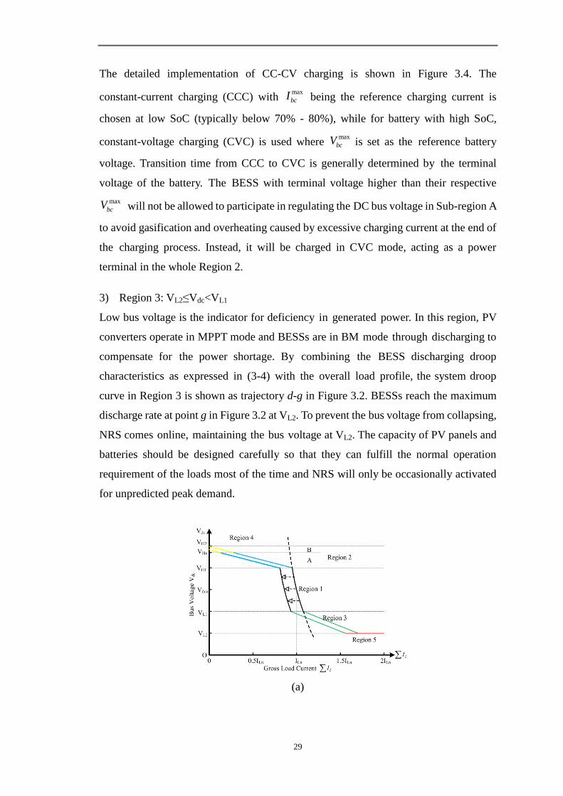
29
The detailed implementation of CC-CV charging is shown in Figure 3.4. The
constant-current charging (CCC) with max
bcI being the reference charging current is
chosen at low SoC (typically below 70% - 80%), while for battery with high SoC,
constant-voltage charging (CVC) is used where max
bcV is set as the reference battery
voltage. Transition time from CCC to CVC is generally determined by the terminal
voltage of the battery. The BESS with terminal voltage higher than their respective
max
bcV will not be allowed to participate in regulating the DC bus voltage in Sub-region A
to avoid gasification and overheating caused by excessive charging current at the end of
the charging process. Instead, it will be charged in CVC mode, acting as a power
terminal in the whole Region 2.
3) Region 3: VL2≤Vdc<VL1
Low bus voltage is the indicator for deficiency in generated power. In this region, PV
converters operate in MPPT mode and BESSs are in BM mode through discharging to
compensate for the power shortage. By combining the BESS discharging droop
characteristics as expressed in (3-4) with the overall load profile, the system droop
curve in Region 3 is shown as trajectory d-g in Figure 3.2. BESSs reach the maximum
discharge rate at point g in Figure 3.2 at VL2. To prevent the bus voltage from collapsing,
NRS comes online, maintaining the bus voltage at VL2. The capacity of PV panels and
batteries should be designed carefully so that they can fulfill the normal operation
requirement of the loads most of the time and NRS will only be occasionally activated
for unpredicted peak demand.
(a)

30
(b)
Figure 3.5. Illustration of impact of PV generations reduction on DC bus characteristics:
(a). the drawback of HLI control; (b). the improvement in HLII control.
Due to the lack of communication link in HLI, optimal operation fashion can hardly be
achieved. Firstly, the system I-V curve should be determined by the real-time BESS
charging/discharging capabilities and PV maximum power outputs. Determination of
droop coefficients is not optimal solution. For example, in case of reduced power
generation from PV modules as shown in Figure 3.5(a), I-V curve will shift leftwards
and the total PV droop curve will intersect with the voltage axis below VH2. The extreme
case is when both voltage regulation zones for PV modules and BESSs are reduced if PV
generations reduced below battery charging capability. This results in degradation of
power sharing accuracy among multiple PV modules or BESSs.
(a)

31
(b)
Figure 3.6. Impact of BESS charging capability reduction: (a). the drawback of HLI
control; (b). the improvement in HLII control.
Secondly, the charging capability of BESS varies with SoC and terminal voltage. The
entire charging capability of BESSs in Sub-region A may be reduced due to several
factors. For instance, some of BESSs with relatively high SoC cannot regulate the bus
voltage according to the predetermined droop equation since the voltage for triggering
CVC is reached. The BESSs in this situation are operating in CVC mode and storing
lower power with respect to the expected stored power in BM mode. Furthermore, the
droop coefficient in Sub-region A is calculated based on the maximum BESSs charging
capacity, which however, might be reduced with the BESS terminal voltage reduction.
In case of charging capacity reduction, the system droop curve in Sub-region A will end
at point p as shown in Figure 3.6 (a) where all BESS elements reach their maximum
charging capacity. The system droop curve then lies along trajectory p-q. PV modules
are activated to operate in BM mode at q. In this case, the system droop curve in
Sub-region B will start at q with the predefined droop coefficient. This may lead bus
voltage to exceed the maximum value VH2 if the entire load becomes quite light as
explicated by trajectory q-r in Figure 3.6 (b).
Thirdly, to prolong the batteries lifetime, it is profitable to prioritize batteries with
different SoCs. Batteries with lower SoC should be scheduled to charge first or fast in
the charging stage to prevent sulphation in extreme low SoC, and vice versa. This
process requires information exchange and coordination control among BESS
converters. The above problems, inherently existing in HLI control, can be compensated
by HLII control as follows.

32
3.3.2. Hierarchical level II (HLII) control
The aforementioned limitations in HLI control can be improved through real-time
information exchange among converters in HLII control. Communication link
generally brings full observability over DC grid including real-time bus voltage, power
flow and operation status of converters. System optimal operation in terms of
reliability and cost can therefore be achieved through coordination control of system
elements. Although the effectiveness of the system operation depends heavily on the
communication quality in HLII, the system reliability would not be degraded due to
HLI as back up. Once failure happens in the communication links, all elements
including PV modules and battery storages can retain the system reliability under HLI
control at the cost of losing global optimal fashion.
The control strategy for Region 1 in HLII is the same as the one in HLI. The PV
modules operate in MPPT mode and BESSs are idled. The main objective of HLII
control is to solve the power sharing problems among PV modules and BESSs
considering their instant capacities variations.
1) Charging/Discharging Control in Regions 2 and 3
Since BESSs need to regulate bus voltage through charging/discharging in Regions 2
and 3, the coordination control among BESSs modules is required. Different
charging/discharging control schemes can be implemented based on special
requirements of BESSs. In this chapter, the control objective is to balance SoCs of
different BESSs through proportional charging/discharging. This objective is achieved
by tuning charging/discharging droop coefficients based on real-time SoCs
measurements and exchanging. An index ξj, which is the ratio of SoCj of jth
BESS to the
average SoC of all BESSs batteries is defined as
1
1
j
j n
j
j
SoC
SoCn
(3-8)
where n is the number of BESSs. Largerξj means the BESS with higher SoC. The ξj is
used to adjust the droop coefficient of jth
BESS converter as

33
'
, 0
, 0
j bj bj
bj
bj j bj
m im
m i
(3-9)
where bjm is the droop coefficient of jth
BESS converter in HLI control as expressed in
(3.6), '
bjm is the modified droop coefficient of jth
BESS converter. The effect of
modified droop coefficient on charging/discharging rate is illustrated in Table 3.2.
Table 3.2. Illustration of SoC-based droop coefficient.
ibj < 0 (charging) ibj > 0 (discharging)
ξj < 1 '
bjm < bjm '
bjm > bjm
ξj > 1 '
bjm > bjm '
bjm < bjm
During charging stage (ibj < 0), the BESS whose SoC is higher than the average SoC of
all BESSs (ξj > 1), is expected to have a lower charging rate. Therefore positive droop
coefficient should be increased from the original ('
bjm > bjm ). This is guaranteed by
equation (3-9) because of ξj > 1. Otherwise, a smaller droop coefficient ('
bjm < bjm ) is
required for the BESSs with lower SoC. Conversely, during discharging stage (ibj > 0), a
smaller droop coefficient ('
bjm < bjm ) promises larger discharging power for those
BESSs with the SoC above the system average SoC (ξj > 1), whereas a relative larger
droop coefficient ('
bjm > bjm ) promises relative small discharging power for the BESS
with the SoC below the system average SoC (ξj < 1).
2) Balancing Voltage Regulation Zones for BESSs and PV Modules
To overcome the problems in HLI control in Region 2, the voltage regulation zones of
BESS and PV converters are assigned proportionally to their instant capacities. As
mentioned in Figure. 3.5(a), the voltage regulation zone of PV converters will be
limited in Sub-region B due to the reduced generation in PV modules. Under HLII
control, the combined system droop is expected to start from VH1 and end at VH2 as
demonstrated in Figure 3.2 regardless of the variations in PV generations to fully

34
utilize the voltage regulation zone. Therefore, the power sharing accuracy can be
enhanced. This can be realized by shifting the threshold value VHx upward to VHx’ as
shown in Figure 3.5(b). VHx’ is determined by interpolation of the DC bus voltage
proportionally to real-time PV maximum power and battery charging capacity. The
ending point in Sub-region B then moves to point b, also meeting the criterion (3.5),
whilst the voltage regulation zone of PV converters can thus occupy the band
completely between VHx’ and VH2 as shown by trajectory a-b in Figure 3.5(b).
The shortcoming of HLI as demonstrated in Figure 3.6(a) can be overcome as well by
HLII control as shown in Figure 3.6(b). This prevents the system droop curve from the
tendency to lie on the trajectories p-q and q-r, which may exceed the maximum
boundary of DC bus voltage. Instead, the system droop curve will move along trajectory
p-s.
3.3.3. Hierarchical level III (HLIII) control
Over- or under-voltage occurs due to sudden loss of loads or PV modules during
normal system operation. This will damage the system elements and cause malfunction
in control system. To prevent abnormal system operation, HLIII control is designed to
maintain the bus voltage within an allowable band once abnormal system conditions
occur.
1) Region 4: Vdc>VH2
When the bus voltage reaches VH2, the ballast is activated to absorb the power and
maintain the voltage within VH2.
2) Region 5: Vdc<VL2
Voltage drop is caused by power deficiency. If all available sources including the NRS
cannot supply the total load, bus voltage will dip below VL2. In this case, a load shedding
scheme is employed to cut part of the non-critical load in order to maintain the bus
voltage within limit. Loads can be prioritized according to their importance and can be
shut down sequentially during load shedding. Prioritization could be realized through
EMS.

35
In summary, reliable and economical operation of a DC microgrid is guaranteed by the
proposed hierarchical control scheme. During the normal operation, the DC microgrid
operates under HLII control, where maximum energy from PV modules is harvested and
the BESSs are coordinately utilized according to their instant SoCs and capacities. Once
a failure occurs in the communication links, the grid is automatically transferred into
HLI control, where each power module will operate based on the thresholds to maintain
basic operations. The emergency conditions are managed by the HLIII control.
3.4. Modeling of System Elements
3.4.1. Modeling of PV arrays
The PV arrays, which convert light into electricity, can be represented as a single diode
model as shown in Figure 3.7(a).
phI D
DI
pR
sR
pvV
pvI
(a) (b)
pvVpvI
Figure 3.7. PV modeling: (a). equivalent circuit of a solar cell, (b). symbol of PV
arrays.
The relationship between the output current and voltage for ns series and np parallel
connected PV arrays can be expressed as the following three equations [68]:
[exp(( / )( / )) 1]pv p ph p sat pv s sI n I n I q AkT V n IR (3-10)
( ( )) /1000ph sso i rI I k T T S (3-11)
3= ( / ) exp(( / ) (1/ 1/ ))sat rr r gap rI I T T qE kA T T (3-12)
where Ipv and Vpv are the output current and voltage of the PV arrays, respectively, ns
and np are the number of cells connected in series and parallel, respectively. S is the
solar irradiation level and T is the temperature of cells.
Based on the solar cell model, I-V and P-V characteristics of PV arrays under a

36
specific solar irradiation level and temperature are obtained as shown in Figure 3.8.
The output current and voltage of PV arrays at certain load condition vary with solar
irradiation and temperature.
Figure 3.8. I-V and P-V characteristics of PV arrays.
3.4.2. Modeling of batteries
The battery model is modeled as a controlled voltage source in series with a constant
resistance as shown in Figure 3.9. Its output voltage depends not only on the current but
also on the battery SoC, which is a nonlinear function of the current and time as
expressed as follows [69]:
o exp( )b b b b
b
QV E R i K A B i dt
Q i dt
(3-13)
100(1 )bi dt
SOCQ
(3-14)
where, Rb is the internal resistance of the battery, E0 is the open circuit potential,
ib is the charging/discharging current of battery, K is the polarization voltage, Q is
the battery capacity, A is the exponential voltage, and B is the exponential
capacity.
3.4.3. Modeling of non-renewable source (NRS)
An ideal DC source as shown in Figure 3.10 is used to represent NRS, serving as the
0 5 10 15 20 25 30 350
2
4
6
8
10
Voltage (V)
Cu
rren
t (A
)
0 5 10 15 20 25 30 350
50
100
150
200
250
Po
wer
(W)
(Vm,Im)
(Vm,Pm)
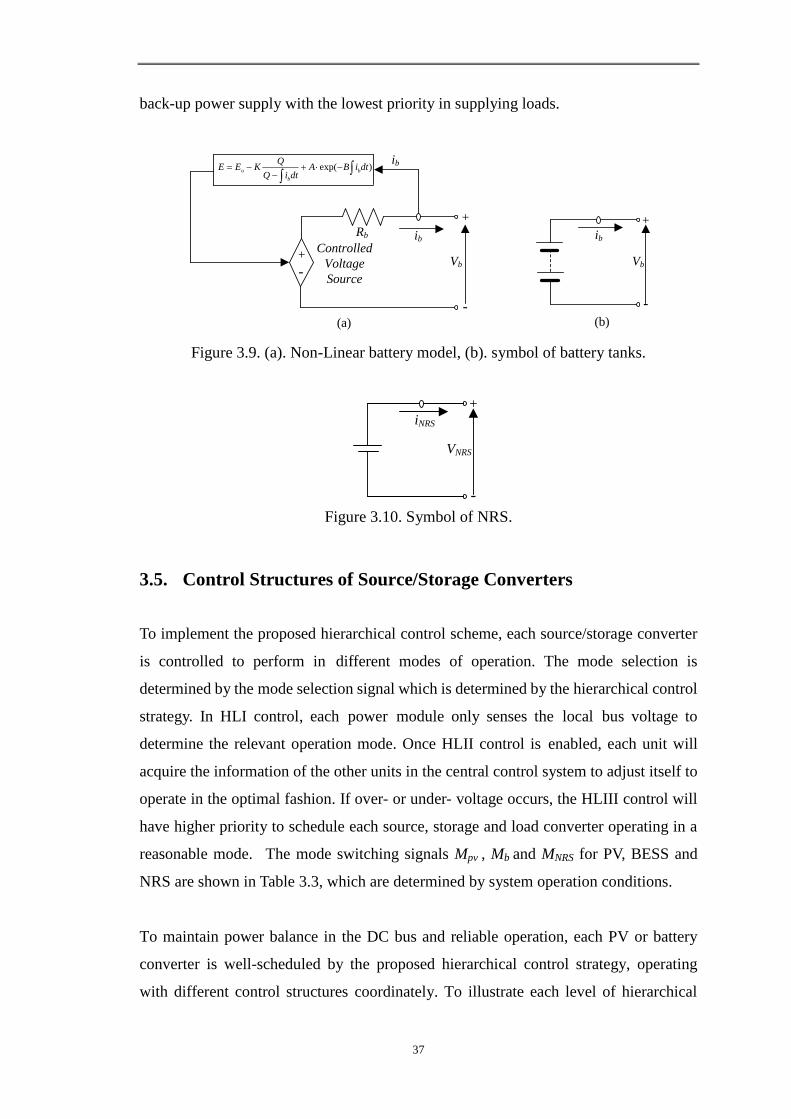
37
back-up power supply with the lowest priority in supplying loads.
+
-
ibRb
Controlled
Voltage
Source
Vb
+
-
ibo exp( )b
b
QE E K A B i dt
Q i dt
ib
+
-
Vb
(a) (b)
Figure 3.9. (a). Non-Linear battery model, (b). symbol of battery tanks.
iNRS
+
-
VNRS
Figure 3.10. Symbol of NRS.
3.5. Control Structures of Source/Storage Converters
To implement the proposed hierarchical control scheme, each source/storage converter
is controlled to perform in different modes of operation. The mode selection is
determined by the mode selection signal which is determined by the hierarchical control
strategy. In HLI control, each power module only senses the local bus voltage to
determine the relevant operation mode. Once HLII control is enabled, each unit will
acquire the information of the other units in the central control system to adjust itself to
operate in the optimal fashion. If over- or under- voltage occurs, the HLIII control will
have higher priority to schedule each source, storage and load converter operating in a
reasonable mode. The mode switching signals Mpv , Mb and MNRS for PV, BESS and
NRS are shown in Table 3.3, which are determined by system operation conditions.
To maintain power balance in the DC bus and reliable operation, each PV or battery
converter is well-scheduled by the proposed hierarchical control strategy, operating
with different control structures coordinately. To illustrate each level of hierarchical

38
control clearly, different control structures, which are employed for proper control of
PV/storage converters at different modes, are described in detail below.
Table 3.3. Mode Selection for PV, BESS and NRS Converters.
1 2 3 4
MPV MPPT Idle BM —
Mb BM Idle CCC CVC
MNRS BM Idle — —
3.5.1. Control of modular PV DC/DC converters
The PV converter is a DC/DC booster as shown in Figure 3.15 and it can operate in
MPPT, BM or idle mode according to the hierarchical control scheme elaborated above.
The control structure of MPPT and BM are described in the following sub-section.
1) MPPT control (MPV = 1)
As described in Section 3.4.1, the output current and voltage of PV arrays vary with
the environmental and loading conditions. In a specific environmental condition, the
PV arrays have a sole maximum power point (MPP) which satisfies:
, 0PV m PV m
PVI I V V
PV
dP
dV (3-15)
IPV
VPV VLoad
ILoad
RLoad
Figure 3.11. Equivalent circuit of the operation of PV arrays.
The MPP in a specific environmental condition is therefore solely dependent on the
loading condition. Figure 3.11 is the equivalent circuit of the operation of PV arrays.
The relevant I-V characteristics of both PV and loads are drawn in Figure 3.12. The
intersection point of two I-V curves is the system operation point. Note that the PV

39
arrays will not operate in MPP if the corresponding loading condition is mismatched.
To extract the maximum available power from PV arrays, the load of the PV system
must be adjusted accordingly so that the load I-V curve intersects the PV I-V curve at
the MPP. To achieve this feature, power electronic interfaces are employed to
interconnect PV arrays and loads as shown in Figure 3.13 where a DC/DC converter is
programmed to regulate the loading condition based on various MPPT algorithms.
Figure 3.12. Illustration of different operation points for PV arrays.
IPV
VPV VLoad
ILoad
RLoad
=
=DC/DC
Figure 3.13. Common PV system with the feature of MPPT.
To realize maximum utilization of solar energy, MPPT techniques are critical for
obtaining maximum power from PV arrays under any given environmental condition.
Basic MPPT algorithms such as constant voltage (CV), perturb and observe (P&O),
incremental conductance (INC) have been widely used in various PV applications [70],
while advanced MPPT variants have been investigated and proposed in many
publications [71-73]. Since the emphasis of this research work is the development of a
coordination control among power modules in the system level, development of new
MPPT algorithms for individual power converter will not be considered. Among the
mature MPPT techniques, The CV method offers stable performance but suffers from
0 5 10 15 20 25 30 350
1
2
3
4
5
6
7
8
9
Voltage (V)
Cu
rren
t (A
)
PV I-V
Load I-V

40
inaccurate maximum power tracking under different environmental conditions. The
INC method offers good performance under rapidly changing environmental
conditions. However, four sensors are required to implement the algorithm. Moreover,
the duration of MPPT process depends on the sensors conversion time. During tracking
time, the PV output is less than its maximum power, which indicates that longer
conversion time will cause larger amount of power loss. The execution speed of P&O
method is relatively higher as only two sensors are required. It gives the benefit of the
reduction of hardware implementation and cost. The P&O method is adopted due to
the advantage of simple arithmetic and easy implementation. For the P&O algorithm,
the perturbation objective can either be PV voltage or current, however, this would be
accompanied with complex implementation. To reduce the complexity, the duty ratio
of interface converter is usually directly perturbed.
Measurements IPV, VPV
Power CalculationP(k)=VPV(k)IPV(k)
P(k)-P(k-1)>0No Yes
VPV(k)-VPV(k-1)>0 VPV(k)-VPV(k-1)>0
d(k+1)=d(k)-Δd
NoYes Yes No
P(k)-P(k-1)=0
Yes
No
P(k)=P(k-1)
Return
d(k+1)=d(k)+Δd d(k+1)=d(k)+Δd d(k+1)=d(k)-Δd
Figure 3.14. Flowchart of P & O algorithm.
The principle of P&O algorithm is first reviewed as: 1). when the duty ratio is
increased by a perturbation step, if the output power of PV array increases, the duty
ration should be increased further. Otherwise, the duty ratio should be decreased; 2)

41
when the duty ratio is decreased by a perturbation step, if the output power of PV array
increases, the duty ration should be decreased further. Otherwise, the duty ratio should
be increased. Based on the above description, the P&O algorithm can be expressed as
1 1( )( )k k k k k kd d d sign d P P (3-16)
where 1k k kd d d is the step size for the perturbing duty ratio; ( ) ( )k PV PVP V k I k is
the PV output power at kth
interval. The relevant flowchart of the P&O algorithm is
illustrated in Figure 3.14.
2) BM control (MPV = 3)
The objective of BM control of PV modules is to regulate the DC bus voltage by
maintaining the power balance in the overall system and to ensure proportional power
outputs from PV modules.
The droop control method in BM mode is employed for proportional power outputs
among multiple PV modules as expressed in (3-7). The I-V droop control generally
senses the output current of PV converter and calculates the voltage reference which is
fed into the inner current-regulated and outer voltage-controlled loops to generate the
required duty ratio dBM. For controller implementation, the proportional-integral (PI)
controller is used for both current and voltage regulators as shown in Figure 3.15.
C1
Ipv
Vpv
D1 D2
C2
LIpv
Vdc
+
-
+
-
Equ. (3-7) +-
PI +-
PI
PWM
ILIo
I-V Droop
+
-
--
ref
pvjV
Figure 3.15. BM control for PV modules.
The control structure of MPPT and BM modes for PV modules have been described

42
above. The PV modules can also operate in idle mode in the case of serious shaded
condition or maintenance duration. The combine the control structures and their
associated mode selection signals as well as the overall control diagram of PV modules
are drawn in Figure 3.16.
Figure 3.16. Mode selection and control diagram of PV modules.
3.5.2. Control of bidirectional DC/DC battery converters
The interface of the battery is a bidirectional buck/boost converter as shown in Figure
3. 17. The battery is connected to the universal half-bridge through an inductor L in the
low voltage terminal. A filter capacitance CO in the high voltage terminal is connected
to the DC bus via the electrical cable. The bidirectional buck/boost converter contains
an individual buck and a boost converter, allowing the battery to freely discharge or
charge according to the specific control structure.
+
-Vdc
IOIb
Vb
L
COS1
S2
Pb
Figure 3.17. Bidirectional DC/DC battery converter.
The operating principle of the battery converter is demonstrated in Figure 3.18. During
discharging, the buck/boost converter operates in booster mode, managing the battery
to release power to the DC grid. The power flow thereby is from the battery to the grid.
During charging, the buck/boost converter operates in buck mode, allowing the battery
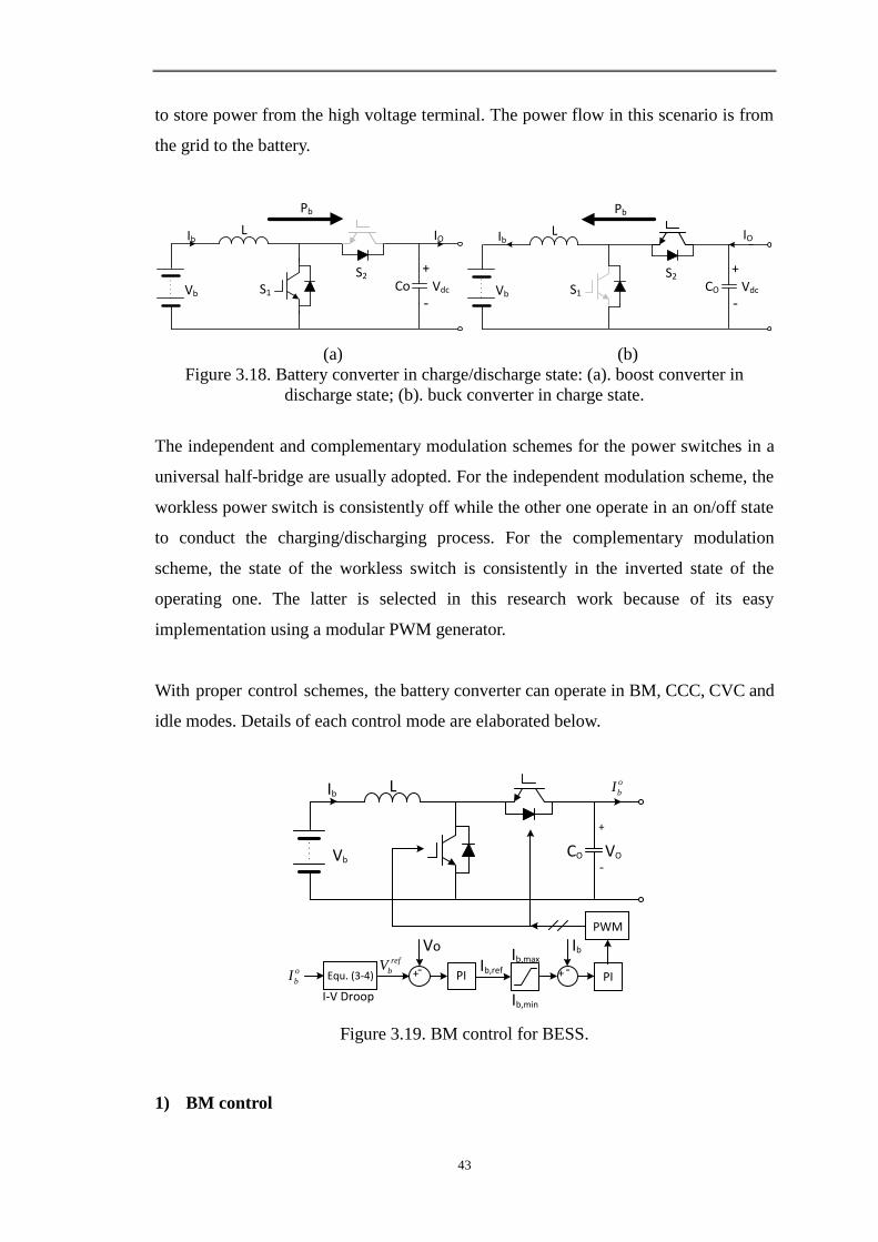
43
to store power from the high voltage terminal. The power flow in this scenario is from
the grid to the battery.
+
-Vdc
IOIb
Vb
L
CoS1
S2+
-Vdc
IOIb
Vb
L
COS1
S2
Pb Pb
(a) (b)
Figure 3.18. Battery converter in charge/discharge state: (a). boost converter in
discharge state; (b). buck converter in charge state.
The independent and complementary modulation schemes for the power switches in a
universal half-bridge are usually adopted. For the independent modulation scheme, the
workless power switch is consistently off while the other one operate in an on/off state
to conduct the charging/discharging process. For the complementary modulation
scheme, the state of the workless switch is consistently in the inverted state of the
operating one. The latter is selected in this research work because of its easy
implementation using a modular PWM generator.
With proper control schemes, the battery converter can operate in BM, CCC, CVC and
idle modes. Details of each control mode are elaborated below.
+
-VO
Ib
Vb
L
CO
+- PI + -PI
Vo Ib
I-V Droop
Ib,max
Ib,min
Ib,ref
PWM
Equ. (3-4)o
bI
o
bI
ref
bV
Figure 3.19. BM control for BESS.
1) BM control

44
The control objective of BM control for BESS is to regulate the DC bus voltage
through maintaining power balance in the overall system and proportionally
absorb/release the surplus/stored power from/to the DC grid. The control block
diagram of BM control is drawn in Figure 3.19. It comprises of a fast inner PI current
controller and a slower outer PI voltage controller. The outer PI controller regulates the
output voltage of the converter through tracking the reference voltage, which is
determined by the V-I droop equation expressed in (3-4). The duty ratio dBM is
subsequently obtained. The current upper and lower limits (max
bI ,min
bI ) are also included
in current control loop to avoid over-current charge/discharge.
2) CCC and CVC during charging stage
In CCC mode, the control objective is to maintain the maximum charging current. The
required duty ratio dCCC for operation is generated by a PI current regulator as shown in
Figure 3.20(a). In CVC mode, the control structure as shown in Figure 3.20(b) is the
same as the voltage controller in BM mode except that the control variable is the
terminal voltage of battery rather than the bus voltage in BM mode. The required duty
ratio dCVC for the battery converter in CVC is similarly generated. The BESS can also
operate in idle mode in Region 1 or in case of over-current charging or under-voltage
discharging. The control diagram of the multi-mode battery converter can be drawn
with the mode selection signals as shown in Figure 3.21.
+- PIIb,c
PWM
Ib
+- PI PWM
Ib
Vb,c+- PI
Vb
(a) (b)
Figure 3.20. Block diagram of CC and CV controls during BESS charging stage.

45
Figure 3.21. Mode selection and control diagram of BESS units.
3.5.3. Control of non-renewable source (NRS) converters
The NRS is interfaced to the DC bus through a DC/DC boost converter and it operates
in the idle mode in most situations. It is only activated online in the case of all PVs and
BESSs cannot meet the total load demand. The control diagram is shown in Figure
3.22. VL2 is the voltage reference of voltage controller. IL is the current flowing on the
inductor of the converter. dBM is the required duty ratio. MNRS is the mode selection
signal of NRS converter.
The control structure in BM mode is the same as the one for the other modules operating
in BM mode except that the reference voltage is fixed rather than the ones determined by
the external I–V droop control loop. Similarly, the mode selection signal can be
scheduled to determine the appropriate operation mode.
Figure 3.22. Mode selection and control diagram of NRS units.
3.6. Hardware Implementation for Verifications
3.6.1. Prototype of a lab-scale DC microgrid
To verify the proposed hierarchical control scheme, experimental tests based on a
scaled-down DC grid have been carried out in WERL. As shown in Figure 3.23, the DC
grid consists of two parallel PV modules, a BESS and a backup DC source as NRS.

46
The hardware set up of the DC grid with sources, converters, central control system and
loads are shown on the top of Figure 3.24. The individual components are shown at the
bottom. Three-channel modular PV converters, controlled by Silicon Labs C8051F120
microcontroller, have been developed as shown on the left bottom side of Figure 3.24.
The maximum power rating of each channel is 2.5 kW. Two channels are configured as
PV converters and the remaining one is used as NRS converter. A bidirectional
buck-boost converter as shown in the middle bottom is developed as the BESS converter.
A PV simulator with two output channels is used to emulate two PV panels. A 16×12V
lead-acid battery bank with 200V nominal operating voltage serves as the BESS as
shown on the right bottom side of Figure 3.24.
Figure 3.23. Configuration of a scale-down DC grid.
Figure 3.24. Lab scale implementations for experimental testing.
A central control system and a DC grid graphic user interface are developed as shown in
the middle bottom of Figure 3.24. The DC grid interface serves as a central monitor and
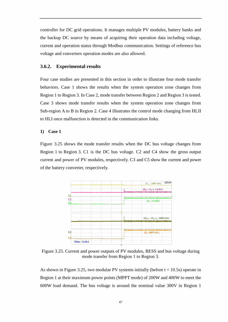
47
controller for DC grid operations. It manages multiple PV modules, battery banks and
the backup DC source by means of acquiring their operation data including voltage,
current and operation status through Modbus communication. Settings of reference bus
voltage and converters operation modes are also allowed.
3.6.2. Experimental results
Four case studies are presented in this section in order to illustrate four mode transfer
behaviors. Case 1 shows the results when the system operation zone changes from
Region 1 to Region 3. In Case 2, mode transfer between Region 2 and Region 3 is tested.
Case 3 shows mode transfer results when the system operation zone changes from
Sub-region A to B in Region 2. Case 4 illustrates the control mode changing from HLII
to HLI once malfunction is detected in the communication links.
1) Case 1
Figure 3.25 shows the mode transfer results when the DC bus voltage changes from
Region 1 to Region 3. C1 is the DC bus voltage. C2 and C4 show the gross output
current and power of PV modules, respectively. C3 and C5 show the current and power
of the battery converter, respectively.
Figure 3.25. Current and power outputs of PV modules, BESS and bus voltage during
mode transfer from Region 1 to Region 3.
As shown in Figure 3.25, two modular PV systems initially (before t = 10.5s) operate in
Region 1 at their maximum power points (MPPT mode) of 200W and 400W to meet the
600W load demand. The bus voltage is around the nominal value 300V in Region 1

48
during this period. BESS operates in idle mode with zero output current (as shown in
C3). At t = 10.5s, the load increases from 600W to 1100W and power generation
deficiency occurs instantly. The equivalent bus capacitor temporarily supplements the
power deficiency by releasing its power. This causes the bus voltage to drop below the
threshold value, 285V (as shown in C1), which activates the battery converter to operate
from idle mode to BM mode. BESS is then maintaining the bus voltage at about 280V
through discharging approximate 500W (to see C5) to load. During the transient state,
negative dv/dt in the equivalent bus capacitor leads to surge current injection into the
output current of PV converters. Combination of the surge current and the maximum
current from PV modules are reflected in the transient state as shown in C2. The surge
currents are also reflected on the output power of PV converters as shown in C4.
2) Case 2
Figure 3.26 shows the results when the DC bus voltage changes from Region 2 to
Region 3. C1 is the DC bus voltage. C2 and C5 show the current and power of battery
converter, respectively.
In this case, the total maximum power of modular PV systems is approximate 900W.
Equivalent DC load includes a fix load with 500W and a variable load with 600W. As
shown in Figure 3.26, the DC bus voltage is initially maintained at around 320V by
battery converter before t = 6s. Both PV modules in this period are operating in MPPT
mode, providing power to the fixed load (500W) and battery charging (400W). At t = 6s,
the variable load becomes online and the entire load increases from 500W to 1100W,
causing the DC bus voltage to drop below the threshold value VL1=285V. At this
moment, the battery converter in reverse regulates the DC bus voltage at around 282V
by supplying approximately 220W of surplus power to the entire load demand.

49
Figure 3.26. Current and power outputs of BESS and bus voltage during mode transfer
between Region 2 and Region 3.
3) Case 3
Figure 3.27 shows the results when the battery converter changes from BM mode to
CCC mode. C1 is the dc bus voltage. C2 and C4 show gross output current and power
of PV modules, respectively. C3 and C5 show the current and power of battery
converter, respectively.
In this case, the total maximum power from two modular PV systems is configured at
1200W. The fixed load is set at 200W while the variable load is set at 600W. The
maximum allowable charging current for the battery is set at 4A. Therefore, the
maximum charging power that BESS can absorb is about 4A×200V=800W. The
experimental results are shown in Figure 3.27. Two PV modules are operating in MPPT
mode, generating approximate 1200W power before t = 5s. Both the fixed and variable
loads, whose total amount of power is about 800W, are online during this period. The
BESS therefore absorbs nearly 400W power to maintain the DC bus voltage at around
320V. At t = 5s, the variable load goes offline. This causes the charging current to
increase and eventually reaches the maximum charging current. Operation mode of
BESS changes from BM to CCC mode. The threshold current is set to be 10% higher
than 4A to prevent malfunction. System power surplus induces voltage increase over
VHx which enables the PV modules changing from MPPT to BM to rebalance system
power. In steady state, the PV modules are maintaining the DC bus voltage at around
327V and BESS operates as a power terminal with charging power of 850W.

50
Figure 3.27. Transient performances of battery converter from BM mode to CCC mode.
The parallel modular PV systems consequently monitor the bus voltage by generating
about 450W. A variable load is turned on at t=14s. At this moment, the BM controlled
PV converters attempt to maintain the system power balance through increasing their
output powers to the maximum value. Power supply deficiency then results in bus
voltage drop. The bus voltage continues dropping to below VHx, which enables the
mode change of BESS and PV modules simultaneously. Subsequently, PV modules
operate at MPPT mode, whilst BESS operates at BM mode in Sub-region A.
4) Case 4
Figure 3.28 shows the results when the DC microgrid is switched from HLII to HLI
control once malfunction is detected in communication links. The experimental data is
measured by a DC meter with data acquisition frequency of 10 Hz and stored in the
database of the central management system for further analysis.
Figure 3.28. Experimental illustration when dc microgrid is controlled from HLII to HLI

51
during communication failure.
In Figure 3.28, he installed maximum power of PV modules is around 3kW, the
maximum charging power of the storage is about 1.03kW, and the load is now
configured at 0.53kW. In HLII, the instant maximum power of PV modules is set at 2kW.
According to equation (3-5) by replacing the maximum values with instantaneous
powers, the VHx is calculated at about 322.5V. The storage is operating at maximum
current charging mode, while PV modules are operating at BM (off-MPPT) mode,
monitoring the DC bus voltage at around 325.7V through generating approximately
1.58kW power to feed the load and storage at around 0.53kW and 1.03kW, respectively.
A mode transfer switch is enabled at 1.4 minutes to mimic the communication failure,
the system control then changes from HLII to HLI. The threshold value VHx in HLI is
calculated using the rated capacities of all modules, which forces bus voltage to be
controlled at 322.7V. The system finally reaches at a new operating point. As a
consequence, the higher resolution of voltage distribution has been proved by HLII and
enhanced system redundancy is achieved by HLI.
3.7. Conclusions
This chapter introduces a hierarchical control strategy for reliable and effective
operations of a standalone DC microgrid. The features of the proposed hierarchical
controlled DC microgrid can be summarized as: 1) maximal usage of renewable energy
and reliability enhancement is achieved by HLI control; 2) real-time voltage regulation
capability for power modules and prioritizations for charging/discharging of the BESS
with different SoCs are considered in HLII control; 3) emergency conditions are
managed by the HLIII control. Nevertheless, the reliable operation of this DC system
relies heavily on the accurate measurement of the DC bus voltage, which involves DC
voltage sensors with high accuracy. This would undoubtedly increase the system cost.
The inaccuracy and malfunction in voltage sensor may lead to inappropriate operation
of relevant modules, this situation needs to be avoided. With the proposed control
method, a discrete characteristic of the DC bus voltage is described in Figure 4.2.
Finally, the feasibility and effectiveness of the presented coordination control strategies
for reliable and effective operation of standalone DC grids have been verified
experimentally in the laboratory prototype.

52
Chapter 4 Global Power Sharing (GPS) Control for
Autonomous Operation of Hybrid AC-DC microgrids
4.1. Introduction
Reliable operations of DC microgrids under hierarchical control scheme have been
stated in previous chapter. Coupling the DC microgrid into the existing AC
infrastructure with the associated power electronics interfaces forms the scenario —
hybrid AC-DC microgrid. Such a complex system generally employs local controller
for basic operations of power modules in the low layer and high layer energy
management system (EMS) with mass information exchange for overall system
optimization. What if the communication network fails or the realization of
communication is difficult for widely dispersed DG systems in rural and remote areas?
Is there an effective control strategy to maintain reliable operations of hybrid system
without any communication links to avoid system outage?
The droop control method has shown the effectiveness on managing parallel operations
of widely dispersed DG systems with the advantages of independent control without
communication links and reliability improvement of overall system. So far, most of the
references on droop control applied to DG have concentrated on AC grids [74-77],
which is understandable based on the dominant role that AC distribution has long served
in the traditional grid. Although not easily spotted, droop control applied to DC
microgrids has also been proposed more than a decade back , but its popularity has not
grown much since then, until quite recently when a few references have explicitly
discussed about some operating issues of DC grids, other than their droop control. This
interest might grow further due to the proliferation of popular green sources like
photovoltaic (PV) and fuel cells, and energy storages like batteries and ultra-capacitors,
which are all DC by nature. The challenge of hybrid microgrids then is to design a
coordination droop control for the DC sources, AC sources and interfacing converter, so
that power flow is always appropriately managed throughout the whole hybrid
microgrid, regardless of whether the load change is detected in the DC, AC or both
sub-grids. This effort of wireless power tuning on DGs and interlinking converter has
not yet been attempted.
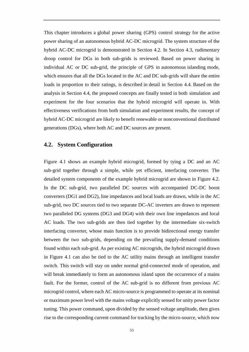
53
This chapter introduces a global power sharing (GPS) control strategy for the active
power sharing of an autonomous hybrid AC-DC microgrid. The system structure of the
hybrid AC-DC microgrid is demonstrated in Section 4.2. In Section 4.3, rudimentary
droop control for DGs in both sub-grids is reviewed. Based on power sharing in
individual AC or DC sub-grid, the principle of GPS in autonomous islanding mode,
which ensures that all the DGs located in the AC and DC sub-grids will share the entire
loads in proportion to their ratings, is described in detail in Section 4.4. Based on the
analysis in Section 4.4, the proposed concepts are finally tested in both simulation and
experiment for the four scenarios that the hybrid microgrid will operate in. With
effectiveness verifications from both simulation and experiment results, the concept of
hybrid AC-DC microgrid are likely to benefit renewable or nonconventional distributed
generations (DGs), where both AC and DC sources are present.
4.2. System Configuration
Figure 4.1 shows an example hybrid microgrid, formed by tying a DC and an AC
sub-grid together through a simple, while yet efficient, interfacing converter. The
detailed system components of the example hybrid microgrid are shown in Figure 4.2.
In the DC sub-grid, two paralleled DC sources with accompanied DC-DC boost
converters (DG1 and DG2), line impedances and local loads are drawn, while in the AC
sub-grid, two DC sources tied to two separate DC-AC inverters are drawn to represent
two paralleled DG systems (DG3 and DG4) with their own line impedances and local
AC loads. The two sub-grids are then tied together by the intermediate six-switch
interfacing converter, whose main function is to provide bidirectional energy transfer
between the two sub-grids, depending on the prevailing supply-demand conditions
found within each sub-grid. As per existing AC microgrids, the hybrid microgrid drawn
in Figure 4.1 can also be tied to the AC utility mains through an intelligent transfer
switch. This switch will stay on under normal grid-connected mode of operation, and
will break immediately to form an autonomous island upon the occurrence of a mains
fault. For the former, control of the AC sub-grid is no different from previous AC
microgrid control, where each AC micro-source is programmed to operate at its nominal
or maximum power level with the mains voltage explicitly sensed for unity power factor
tuning. This power command, upon divided by the sensed voltage amplitude, then gives
rise to the corresponding current command for tracking by the micro-source, which now
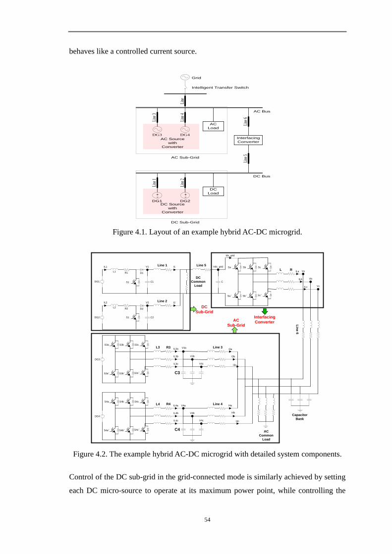
54
behaves like a controlled current source.
Line
3
Line
4
DG3 DG4
Line
AC
Load
Line
1
Line
2
DC
Load
AC Sub-Grid
AC Source
with
Converter
Line
6Li
ne 5
DG1 DG2
+-
+-
DC Source
with
Converter
Interfacing
Converter
DC Sub-Grid
Grid
Intelligent Transfer Switch
DC Bus
AC Bus
Figure 4.1. Layout of an example hybrid AC-DC microgrid.
DG1
L1R1
C1
Line 1
D1
DG2
L2R2
C2
Line 2
D2
DC
Common
Load
Line 5V1
V2
C
Vdc_grid
S1
S1
Sa Sb Sc
Sa’ Sb’ Sc’
Lin
e 6
DG3
S3a S3b S3c
S3a’ S3b’ S3c’
DG4
S4a S4b S4c
S4a’ S4b’ S4c’
Vb
Vc
Line 3
Line 4
Va
IL1 I1
IL2 I2
IL3a
IL3b
IL4c
IL3c
IL4b
IL4a
L3 R3
L4 R4
C3
C4AC
Common
Load
L R
V3a
V3b
V3c
V4a
V4b
V4c
I3a
I3b
I3c
I4a
I4b
I4c
Capacitor
Bank
AC
Sub-Grid
DC
Sub-Grid
ILa
ILb
ILc
Interfacing
Converter
Idc_grid
Figure 4.2. The example hybrid AC-DC microgrid with detailed system components.
Control of the DC sub-grid in the grid-connected mode is similarly achieved by setting
each DC micro-source to operate at its maximum power point, while controlling the
55
interfacing converter to regulate its DC-link voltage using the set of firm three-phase
voltages imposed by the mains. This style of control is no different from a typical solar
generation system, where a DC-DC boost converter for MPPT is connected to a DC-AC
inverter for grid interfacing. Because of that, control of the hybrid microgrid under
grid-connected mode is not expected to be very different, and is therefore not further
considered. Rather, the challenge is to investigate the power management control when
the hybrid microgrid is configured to operate in the autonomous islanding mode, whose
details are elaborated as follows.
4.3. Power Sharing in Individual AC or DC Microgrid
As stated in the introduction section, droop control method is usually applied to the
parallel operation of widely dispersed DG systems. By applying this method, each DG
module can be able to operate independently without line communication through
sensing only the local voltage and current for output power calculation. Thus, the droop
control is also named independent, autonomous, or wireless control [15]. In this section,
the basic principle of preliminary droop control as well as its improved variants is
firstly reviewed and deduced from the theory related to the power flow in the
conventional AC system as follows.
4.3.1. Review of rudimentary droop control
Figure 3.8 shows the equivalent circuit of a voltage controlled PWM inverter connected
to a point of common coupling (PCC) through the line impedance Z. The complex
power drawn to the bus can be expressed as
S P jQ (3-17)
where P and Q are the active and reactive power, respectively, which are given by
2
( )EV V
P cos cosZ Z
(3-18)
2
( )EV V
Q sin sinZ Z
(3-19)

56
where E and V are the amplitudes of the inverter output voltage and common bus voltage,
δ is power angle, and Z and θ are the magnitude and the phase of the equivalent of output
line impedance.
E oV 0
ZjXRi
jQPS
Figure 4.3. Equivalent circuit of a voltage controlled PWM inverter connected to a
common AC bus.
A conventional assumption is to consider that Z is mainly inductive (θ=90°) due to the
inductive output impedance of inverter, which is often justified by the large
filter-inductor value. In this situation, the following well-known expressions of the
active and reactive power can be derived from (4-2) and (4-3), and further simplified by
considering a small phase difference δ between the inverter output voltage E and the
common AC bus voltage V (sinδ = δ and cosδ = 1) [15]:
EV EV
P sinX X
(3-20)
2
( )EVcos V V
Q E VX X
(3-21)
From the above equations, it can be seen that the active power P is primarily dependent
on the power angle δ, while the reactive power Q is mainly influenced by the amplitude
difference E-V. Consequently, most wireless load sharing controllers introduce artificial
droops (also named virtual inertia) into the output voltage reference. Thus, P-ω and Q-V
droop schemes are often adopted. The rudimentary form to implement the droop control
law can be expressed as follows
* *+ ( )m P P (3-22)
* *+ ( )E E n Q Q (3-23)
where 𝜔∗ and 𝐸∗ are the output-voltage frequency and amplitude at no load, and m and
n are the droop frequency and amplitude coefficients. 𝑃∗ and 𝑄∗ are the active and
57
reactive power reference, which are commonly set to zero (𝑃∗ = 0 and 𝑄∗ = 0) when
the parallel inverters work in islanding mode of operation. The droop expressions in
(4-6) and (4-7) become
*+mP (3-24)
*+E E nQ (3-25)
Note that although (4-4) shows a relationship between δ and P, (4-6) uses the frequency
ω instead of δ. This is because the units do not know the initial phase value of the other
units; however, the initial angular frequency at no load can easily be fixed as ω*.
Moreover, the angular frequency ω in (4-8) can be always replaced by the frequency f .
Using this method, it is well known that if the droop coefficients are increased, then
good power sharing is achieved. However, to keep the voltage variations within
acceptable bounds would then requires m and n to be less gradual. Therefore, the best
tradeoff between load sharing accuracy and voltage regulation would require a careful
study of system before tuning m and n. For instance, the acceptable frequency and
amplitude deviations are mostly at 2% and 5%, respectively. Accordingly, m and n are
usually tuned by the following equations
nomm P (3-26)
2 nomn E Q (3-27)
where 𝛥𝜔 and 𝛥𝑒 are the maximum allowed frequency and voltage deviations, and
Pnom and Qnom are nominal P and Q provided by the DG system, respectively. To ensure
proper load sharing according to inverter rating, the droop coefficients have to be
adjusted according to the following relationships [74]
1 1 2 2 3 3 n nm S m S m S m S (3-28)
1 1 2 2 3 3 n nn S n S n S n S (3-29)
where 𝑆𝑖 is the apparent power of the inverter i.
58
The inverter output impedance is usually assumed to be inductive, which is often
justified by the high inductive components of the line impedance and the large
inductance of the output filter. However, this is not always true, since the closed-loop
output impedance also depends on the control strategy, and the line impedance is
predominantly resistive for low voltage levels. Thus, (4-4) and (4-5) can be recalculated
by considering a general output impedance of each inverter Z . By expanding (4-2)
and (4-3), the active and reactive powers injected to the bus by every unit can be
expressed as [78]
2
cosEV V EV
P cos sin sinZ Z Z
( ) (3-30)
2EV V EV
Q cos sin sin cosZ Z Z
( ) (3-31)
Observing from (4-14) and (4-15), the following relationship can be obtained in (4-16)
and (4-17). Similarly, the relationship deduced from (4-14) and (4-15) can be simplified
by considering a small phase difference δ between the inverter output voltage E and the
common AC bus voltage V (sinδ = δand cosδ = 1):
EV EV
Psin Qcos sinZ Z
(3-32)
EV EV
Pcos Qsin sinZ Z
(3-33)
Consequently, the general form of droop control method can be expressed as
*+ ( )m Psin Qcos (3-34)
*+ ( )E E n Pcos Qsin (3-35)
The general droop control expressions (4-18) and (4-19) indicate that the output
impedance angle θ determines specified droop control low, as shown in Table 4.1.

59
Table 4.1. Output impedance impacts over power flow controllability.
Output
impedance
Z=jX
(inductive: θ=90°)
Z=R
(resistive: θ=0°)
Active
Power (P) 𝑃 =
𝐸𝑉
𝑋𝑠𝑖𝑛 𝛿 ≈
𝐸𝑉
𝑋𝛿 𝑃 =
𝐸𝑉 𝑐𝑜𝑠 𝛿 − 𝑉2
𝑅≈𝑉
𝑅(𝐸 − 𝑉)
Reactive
Power (Q) 𝑄 =𝐸𝑉 𝑐𝑜𝑠 𝛿− 𝑉2
𝑋≈𝑉
𝑋(𝐸 − 𝑉) 𝑄 =
𝐸𝑉
𝑅𝑠𝑖𝑛 𝛿 ≈ −
𝐸𝑉
𝑅𝛿
Frequency
Droop (ω) 𝜔 = 𝜔∗ −𝑚𝑃 𝜔 = 𝜔∗ +𝑚𝑄
Amplitude
Droop (E) 𝐸 = 𝐸∗ − 𝑛𝑄 𝐸 = 𝐸∗ − 𝑛𝑃
m 𝛥𝜔/𝑃𝑛𝑜𝑚 𝛥𝜔/2𝑄𝑛𝑜𝑚
n 𝛥𝐸/2𝑄𝑛𝑜𝑚
𝛥𝐸/𝑃𝑛𝑜𝑚
EE
P Q
nomQ
E
nomP nomQ
(a)
EE
P Q
nomQ
E
nomP nomQ
(b)
Figure 4.4. Droop control functions for (a) inductive output impedance and (b) resistive
output impedance.
It can be seen from Table 4.1 that the control lows for different line impedance (Z=jX
and Z=R) are quite different. Table 4.1 specifically demonstrates that a control scheme
based on P-ω and Q-V droops should be used for inductive impedance, while for
resistive impedance the reverse P-V and Q-ω droops are suitable. Thus, the line
impedance has a considerable effect on the power-sharing accuracy of the P/Q droop
method. For this reason, it is important to design the output impedance properly in order
to improve complete decoupling between active and reactive power and consequently
avoid the impact of line impedance on the power sharing [77]. Table 4.1 also shows that

60
the controller gains m and n are chosen as a function of the nominal values of P and Q,
and the acceptable maximum deviations in frequency 𝛿𝜔 and amplitude 𝛿𝐸 .
Accordingly, Figure 4.4(a) and (b) show the droop characteristics for pure inductive
output impedance and resistive output impedance, respectively.
P & Q
Calculation
P~
Q~
LPF
LPF
P
Q
+
+
++
max
min
maxE
minE
Space
Vector
to ABC
E
E
P droop
Q droop
oi
ov
refvn
m
Figure 4.5. Block diagram of the rudimentary droop control method.
Based on the above description on the rudimentary droop control method, the block
diagram of the basic droop method for power sharing among DGs in AC grid is drawn
in Figure 4.5. The output voltage and current are initially measured for calculating the
output active P and reactive power Q, which would be then filtered by low-pass filters in
order to obtain the average active and reactive power. The average powers are then fed
into the droop controllers with deducing the reference ω and voltage magnitude E of the
source inverters. Finally, the reference ω and voltage magnitude E are synthesized to
reference three-phase voltage which perform as the reference value of the voltage source
inverter (VSI) based DGs.
4.3.2. Review of improved variants of droop control
Although the possibility of operation with no communications signals between parallel
DG units is a very attractive feature, the conventional droop method described in last
section has several inherent disadvantages [75, 79]: 1) the load-sharing accuracy is
strongly affected by the output impedance and the line impedance unbalances; 2) the
harmonic power in case of supplying nonlinear load is poorly compensated; and 3) an
inherent tradeoff exists between the load-sharing accuracy and the output voltage
regulation. To overcome the pre-mentioned drawbacks, some improved control
solutions based on rudimentary droop technique have been investigated. This
sub-section will briefly introduced the existing improved droop techniques.

61
1) Droop control with virtual output impedance
It is known that the inverter output impedance has a considerable effect on the
load-sharing accuracy of the P/Q droop method. A possible solution to the line
impedance problem consists of adding an inductor in series with the inverter output [76]
in order to fix the output impedance. However, this inductor is heavy and bulky,
increasing the size and the cost of equipment. Alternatively or complementary to the use
of local signal communications, it is often used as a fast control loop, called virtual
output impedance, which adopt the control solution to fix the output impedance of the
inverter.
P & Q
Calculation
P~
Q~
LPF
LPF'
P
Q
+
+
++
max
min
maxE
minE
Space
Vector
to ABC
E
E
P droop
Q droop
oiov ref
ovm
n
Voltage
loop+
-Curent
loop+PWMVSI
ov
oiZo(s)
*
ov
Li
Figure 4.6. Block diagram of the closed-loop VSI with the virtual output impedance
path.
In theory, this virtual impedance should be larger than the combined values of the output
impedance of the VSI plus the maximum power line impedance. In [77], the virtual
output impedance is expressed as
( )ref
o o o ov v i Z s (3-36)
where ( )oZ s is the transfer function of the virtual output impedance, 𝑣o∗ is the voltage
reference calculated by the P/Q sharing loop, and ref
ov is the voltage reference
provided to the inner voltage control loops. According to (4-20), Figure 4.6 shows the
block diagram of a droop controller with the virtual output impedance loop. The value of
the output impedance must be selected following a similar way as the m and n
coefficients, according to the nominal apparent power Sx of each VSI unit.
1 1 2 2o o on nZ S Z S Z S (3-37)
62
By introducing this virtual impedance to the original control loop, the output impedance
has become a control variable of the DG system.
2) Droop control with power derivative and integral terms
The conventional droop method has several intrinsic problems related to its limited
transient response, since the system dynamics depends on the power-calculation filter
characteristics, the droop coefficients, and the output impedance. These parameters are
determined by the line-frequency, the maximum allowed frequency and amplitude
deviations, and the nominal output power. Thus, by using conventional droop method,
the inverter dynamics cannot be independently controlled. To overcome the dynamics of
the system, the following improved droop control schemes with the power derivative
and integral terms is proposed [80],
t
P d
dPm Pd m P m
dt
(3-38)
d
dQE E nQ n
dt
(3-39)
where 𝑛𝑑 is the derivative coefficient of the reactive power 𝑄; 𝑚, 𝑚𝑝, and 𝑚𝑑 are the
integral, proportional, and derivative coefficients of the active power 𝑃. If 𝜔 = 𝑑∅/𝑑𝑡
is taken into account, the steady-state P/Q droops coincide exactly with those obtained
with the basic droop method as expressed in (4-6) and (4-7). According to (4-22) and
(4-23), the block diagram of droop control with power derivative and integral terms is
shown in Figure 4.7. This proposed control scheme modifies the control expressions,
acting on the transient response, and, at the same time, keeping the static droop
characteristic. Also, it minimizes the transient circulating current among the units and
further improves the dynamic performance of the whole system.

63
P & Q
Calculation
P~
Q~
LPF
LPF' Q
+
+
++
Space
Vector
to ABC
E
P droop
Q droop
oi
ov
refvn
mP
PD
PID dt
dPmPmPdm dp
t
dt
dQnnQEE d
Figure 4.7. Block diagram of improved droop control with power derivative and integral
terms for enhancing system transient stability.
3) Droop control with harmonic current sharing
One of the disadvantages of the conventional droop control method is its poor
load-sharing when supplying nonlinear load. Commonly, the current total harmonic
distortion (THD) can be up to 150%, i.e., the sum of the harmonic current root mean
square (RMS) values can be up to 1.5 times the fundamental harmonic component.
Hence, the parallel DG modules must be able to share these harmonics. If the paralleled
modules cannot ensure sharing of these harmonics, then the system will be severely
degraded in the presence of nonlinear loads. This provides the motivation for sharing the
current distortion components induced by nonlinear loads as well as the fundamental
components associated with both linear and nonlinear loads.
In [75], the distorted power is obtained by subtracting the output active power P, and
reactive power Q from the apparent power S as the following equation
2 2 2D S P Q (3-40)
where D is the distorted power (VA). The distorted power is due to the combination of
voltage and current components of different frequencies. It should be noticed that there
is no active power in these harmonic terms, but reactive power only.
Unlike the fundamental reactive power, the flow of the distortion power cannot be
influenced by adjusting the fundamental component of the inverter voltage alone. One
method of solving this problem is to adjust the gain of the voltage loop as a function of
the distortion power as shown in Figure 4.8.

64
P & Q
Calculation
P~
Q~
LPF
LPF'
P
Q
+
+
++
max
min
maxE
minE
Space
Vector
to ABC
E
E
P droop
Q droop
oiov
m
n
Voltage
loop
Curent
loop+PWMVSI
ov
oi
*
ov
Li
Distorted
Power (D)
calculation222 QPSD
Figure 4.8. Block diagram of droop control with distorted power sharing.
By reducing the gain (and bandwidth) of the voltage loop in the presence of distortion
components, the output impedance in the high-frequency range is increased, and the
harmonic power sharing is automatically done.
4.3.3. Power sharing in AC microgrids
The rudimentary droop control and its advanced variants have been reviewed in
previous sub-sections. For the rudimentary droop control, it generally uses two droop
control equations for deducing its source converter reference frequency f and voltage
amplitude E from the measured active P and reactive power Q, respectively. Assuming
that the line impendence of each DG unit in the AC microgrid is pure inductive, the
basic droop functions for u DG units can be expressed as (4-25) and (4-26) for
illustrative purposes, and drawn in Figure 4.9 for showing the drooping gradients m and
n.
_ x ac xf f m P (3-41)
_x x a c xE E n Q , for x = 1, . . . , u. (3-42)
where subscript x represents the DG index in AC microgrid, f*
and E* are the reference
frequency and voltage amplitude at no load condition, respectively. The reference
frequency is selected as the system maximum allowable frequency fmax, while the
reference amplitude is preferably selected as the nominal operation voltage as shown in
Figure 4.9. Pac_x and Qac_x are the calculated active and reactive power of xth
DG unit,
respectively. And mx and nx are the negative droop coefficients, representing the
negatively tilting gradients as shown in Figure 4.9. The negative droop coefficients can
be designed according to (4-10) and (4-11) as

65
_
min maxx nom
ac x
f fm
P
(3-43)
_2
min maxx nom
ac x
E En
Q
(3-44)
where fmin, fmax, Emin, and Emax are minimum and maximum allowable frequency and
voltage amplitude, respectively. _
nom
ac xP and _
nom
ac xQ are the nominal active and reactive
power for xth
DG unit, respectively.
Considering that the intention of this research work is the development of a control
scheme for GPS based on coordination design on basic droop equations of both
sub-grids, reactive power sharing is henceforth not taken into account. Therefore,
combining (4-25) and (4-27) results in
_1 _ 2 _
_1 _ 2 _
= = =ac ac ac u
nom nom nom
ac ac ac u
P P P
P P P (3-45)
It is indicated in (4-29) that u DG units in AC sub-grid will rightfully share the load
demand in proportion to their nominal powers.
Figure 4.9. Droop characteristics for DGs in AC sub-grid.
Quite obviously, the control objective of sharing power proportionally among the AC
DGs will cause their reference terminal voltages to vary with the grid demanded active
and reactive power. Keeping the voltage variations within acceptable bounds will then
requires the gradients m and n to be less gradual, but that will compromise the load
sharing accuracy. The best tradeoff will therefore require a careful study of the system,

66
before tuning m and n accordingly [81]. As mentioned in last section, an alternative
solution for improving system transient stability is to modify the basic equations of
(4-25) and (4-26) in the way described in [80]. This however is not attempted here,
since the intention is to show that the overall proposed GPS for the hybrid microgrid
works fine even for the simplest droop control case, and is therefore not technically
dependent on any existing advanced features.
Combining the values determined from (4-25) and (4-26) gives rise to the demanded
voltage reference 3_
ref
abcV as explicitly indicated at the top of Figure 4.10. The
constructed voltage reference is then fed to the dual-loop voltage regulator drawn at the
bottom of Figure 4.10, where an inner proportional current loop and an outer
proportional-resonant (PR) voltage loop are drawn. Sizing of control parameters for this
regulator is important, since it affects the tracking accuracy and output impedance.
P & Q
Calculation
3
~P
3
~Q
LPF
LPF
3P
3Q
+
+
++
max
min
maxE
minE
Space
Vector
to ABC
E
E
P droop
Q droop
+-
abcI _3
abcV _3
PR
Voltage
Regulator
3_
ref
aV
3_
ref
bV
3_
ref
cV
aV _3
3_
ref
aV+-P
Current
Regulator
3m
3n
3_
2
dcV
bm~am~
cm~PWM
Modulator aLI _3
Pulses
Pulses
Pulses
Inner current and voltage control
Figure 4.10. Control scheme for AC micro-sources DG3 and DG4.
4.3.4. Power sharing in DC microgrids
Unlike the AC sub-grid, the DC sub-grid is much simpler in the sense that it does not
have reactive power, and the only voltage quantity available for control is its amplitude.
With zero phase and resistive (non-reactive) DC lines, it is clear that active power is no
longer dependent on the frequency, but solely varies with the voltage difference Vdc_y –
Vdc, where Vdc_y is the terminal voltage of yth
DG unit in DC sub-grid and Vdc is the DC
bus voltage. Because of that and as briefly mentioned in [82], active power P sharing

67
among the DC DGs can hence be provided by drooping their DC source voltages Vdc_y
according to (4-30).
*
d c _ _y d c y d c yV V d P , for y = 1, . . . , v. (3-46)
where subscript y represents the DG index in the DC sub-grid, *
dcV is the reference
frequency and configured at the maximum allowable voltage. Vdc_y is the terminal
voltage of yth
DG unit and dy is the negative droop coefficient and is given by
_
min max
dc dcy nom
dc y
V Vd
P
(3-47)
where min
dcV and max
dcV are the minimum and maximum allowable voltages in the DC
sub-grid, respectively. _
max
dc yP is the nominal output power for yth
DG unit.
Unlike an AC system whose frequency is unique throughout the system at steady state,
the terminal voltage of each DG unit in DC microgrid is slightly different due to the
voltage drop across the cable as demonstrated in Figure 4.11(a). This will lead to the
power sharing inaccuracy among DG modules [62]. To solve this inherent problem in
DC system, a modified droop equation is developed as
*
dc_ _ _ _y dc y dc y dc y dc yV V d P i Z (3-48)
where idc_y and Zdc_y are the output current and resistive cable impedance of yth
DG unit,
thus, idc_y Zdc_y is voltage drop on yth
cable. Rearranging (4-32) follows that
* *
dc_ _ _ _ dc _y dc y dc y dc y dc y dc y dc yV i Z V d P V V d P (3-49)
In (4-33), Vdc is the unique DC-bus voltage, performing like the role of frequency in AC
system. The modified droop characteristic is shown in Figure 4.11(b). By modifying the
basic droop expression into (4-33), the accurate power sharing can be established as
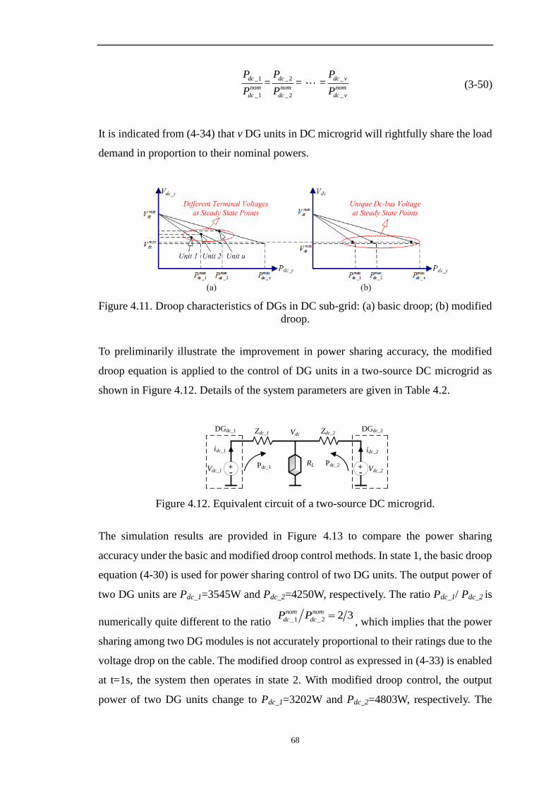
68
_1 _ 2 _
_1 _ 2 _
= = =dc dc dc v
nom nom nom
dc dc dc v
P P P
P P P (3-50)
It is indicated from (4-34) that v DG units in DC microgrid will rightfully share the load
demand in proportion to their nominal powers.
Figure 4.11. Droop characteristics of DGs in DC sub-grid: (a) basic droop; (b) modified
droop.
To preliminarily illustrate the improvement in power sharing accuracy, the modified
droop equation is applied to the control of DG units in a two-source DC microgrid as
shown in Figure 4.12. Details of the system parameters are given in Table 4.2.
+-
DGdc_1
Vdc_1Pdc_1 +
-
Zdc_1
RL
Vdc
Vdc_2
idc_1 idc_2
Zdc_2
Pdc_2
DGdc_2
Figure 4.12. Equivalent circuit of a two-source DC microgrid.
The simulation results are provided in Figure 4.13 to compare the power sharing
accuracy under the basic and modified droop control methods. In state 1, the basic droop
equation (4-30) is used for power sharing control of two DG units. The output power of
two DG units are Pdc_1=3545W and Pdc_2=4250W, respectively. The ratio Pdc_1/ Pdc_2 is
numerically quite different to the ratio _1 _2 2 3nom nom
dc dcP P , which implies that the power
sharing among two DG modules is not accurately proportional to their ratings due to the
voltage drop on the cable. The modified droop control as expressed in (4-33) is enabled
at t=1s, the system then operates in state 2. With modified droop control, the output
power of two DG units change to Pdc_1=3202W and Pdc_2=4803W, respectively. The

69
ratio Pdc_1/ Pdc_2 becomes quite close to the ratio _1 _2 2 3nom nom
dc dcP P , which elucidates
that two DG units can accurately share the DC load in proportion to their ratings by
considering the cable voltage drop in the droop characteristics.
Table 4.2. Parameters of two-source DC Microgrid.
Parameters Value (units)
Nominal Voltage: n
dcV 700V
max
dcV 720V
min
dcV 680V
_1dcZ
1Ω
_ 2dcZ
2Ω
Load Resistor: LR 60Ω
_1
max
dcP
4000W
_ 2
max
dcP
6000W
Figure 4.13. Simulation verifications of modified droop characteristics for DG units in a
two-source DC microgrid.
The control block realization of (4-33) is shown at the top of Figure 4.14, and as per the
AC sub-grid, coefficient d should be tuned appropriately since a steeper slope will lead
to better power sharing, but wider voltage variations, which might not be acceptable by
international specified standards. The voltage reference 1
refV computed by (4-33) for
each DC micro-source is then fed to its voltage regulator drawn at the bottom of Figure
4.14. The voltage regulator consists of an outer PI voltage controller and an inner
proportional current controller, which forces the output voltage of DG to track the
calculated reference voltage.

70
Power
CalculationLPF
++
+-PI
Voltage
Regulator
+-P
Current
Regulator
PWM
Inner current and voltage control
dc _1V
_1dci 1d
maxV
minV
1
refV
1LI
1
refV1d
1
~P 1P
P-V droop
VDG1
Pulses -
_1dcZ
*
dcV
dc _1V
Figure 4.14. Control scheme for DGs in DC sub-grid.
4.4. Global Power Sharing throughout a Hybrid AC/DC Microgrid
4.4.1. Principle of global power sharing
Control schemes described in the earlier two sub-sections will allow the DGs to share
their local loads in the respective sub-grids. Upon knowing power sharing in individual
AC or DC sub-grid, the follow-up requirement is to explore a reasonable rule of power
exchange between two sub-grids. With this in mind, the GPS is subsequently proposed
to realize power sharing throughout both sub-grids, regardless of whether the DGs are
placed in the AC or DC sub-grid. Advantages of such wider scope of power sharing are
summarized as follows [83-85]:
a) Any single point of failure due to overstress in certain source can be avoided;
b) Sources with slower response to load transients are expected to have smaller
variations, thus resulting in short transient period;
c) Design of the capacity of each sub-grid will no longer be constrained by their
respective local load profiles. Rather, their capacities can be chosen according to the
entire load profiles since DGs in one network can be viewed as a back-up reserve
for the another;
d) All elements are managed in a decentralized manner without information exchange.
This provides an emergency operation scheme during communication failures for
complex system with mass communications.

71
The above advantages cannot be achieved by just relying on droop controlled DGs in
individual AC or DC sub-grid. The point becomes to the development of proper
control scheme on power tuning for the interlinking converter (IC).
(a) The IC has to manage bidirectional active power flow between two sub-grids,
where positive and negative polarities stand for forward DC-AC and reverse
AC-DC power flow, respectively. This scenario is different from DGs with
unidirectional power outputs.
(b) At any instant, the IC has to perform two roles. It performs as the supply end to one
sub-grid who absorbs the power from IC, and appear as the demand end to the
other sub-grid who releases the power to IC.
(c) The two sets of droop equations with different y-axis dimensions need to be
derived before arriving at the final active power command to be transferred to the
IC for GPS realization.
The aforementioned complexities can be managed by a normalization process. By
using the normalization method, the principle of GPS is interpreted by means of
mathematical and graphical methods as follows.
In AC sub-grid, summation of all sub-equations in (4-25) while ignoring the power
losses due to switching actions and transmission lines follows the combined AC droop
characteristics as
_
1
u
ac x
x
f f M P
(3-51)
1
11
u
x x
Mm
(3-52)
where _
1
u
ac x
x
P
is the gross active power generated from all u DG units in AC sub-grid.
M is the negatively droop coefficient of combine droop characteristics in AC sub-grid as
shown in Figure 4.15.
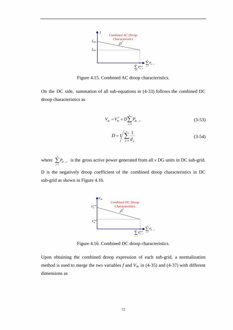
72
Combined AC Droop
Characteristics
fmin
fmax
f
_
1
u
ac x
x
P
_
1
umax
ac x
x
P
Figure 4.15. Combined AC droop characteristics.
On the DC side, summation of all sub-equations in (4-33) follows the combined DC
droop characteristics as
*
_
1
v
dc dc dc y
y
V V D P
(3-53)
1
11
v
y y
Dd
(3-54)
where _
1
v
dc y
y
P
is the gross active power generated from all v DG units in DC sub-grid.
D is the negatively droop coefficient of the combined droop characteristics in DC
sub-grid as shown in Figure 4.16.
Vdc
min
dcV
max
dcV
_
1
v
dc y
y
P
_
1
vmax
dc y
y
P
Combined DC Droop
Characteristics
Figure 4.16. Combined DC droop characteristics.
Upon obtaining the combined droop expression of each sub-grid, a normalization
method is used to merge the two variables f and Vdc in (4-35) and (4-37) with different
dimensions as

73
,
( )'=
,
nn
max n
nn
min n
for
for
(3-55)
where γ represents the variable f or Vdc, ( )' denotes the normalized variable. γn is
variable’s nominal value, and γmax, γmin are the variable’s maximum and minimum
values, respectively. Assuming that γmax and γmin are symmetric compared to γn, (4-39)
can therefore be written as
0.5( )
( )'=0.5( )
max min
max min
(3-56)
Equation (4-40) indicates that the normalized value ( )' varies between -1 and 1.
Substituting the relevant normalized variable into (4-35) and (4-37) follows that
_
1
( )' 10.5( )max
u
a x
xmin
cPM
ff f
(3-57)
_
1
( )' 10.5( )
v
dc ymax minydc dc
dc PV V
DV
(3-58)
(4-41) and (4-42) are the normalized combined droop characteristics of AC and DC
sub-grids, respectively. Recalling the definitions of mx and dy in (4-27) and (4-31),
(4-41) and (4-42) can be transformed to (4-43) and (4-44), respectively, as follows
_
1_
1
1( )' 1-
0.5
u
ac xunom x
ac x
x
P
P
f
(3-59)
_
1_
1
1( )' 1
0.5
v
dc yvnom y
dc
dc
y
y
P
P
V
(3-60)
where _
1
unom
ac x
x
P
, _
1
vnom
dc y
y
P
are summations of the nominal powers of u and v DG units,
respectively. According to (4-43) and (4-44), the normalized droop characteristics of AC
and DC buses are drawn in Figure 4.17(a) and (b), respectively.
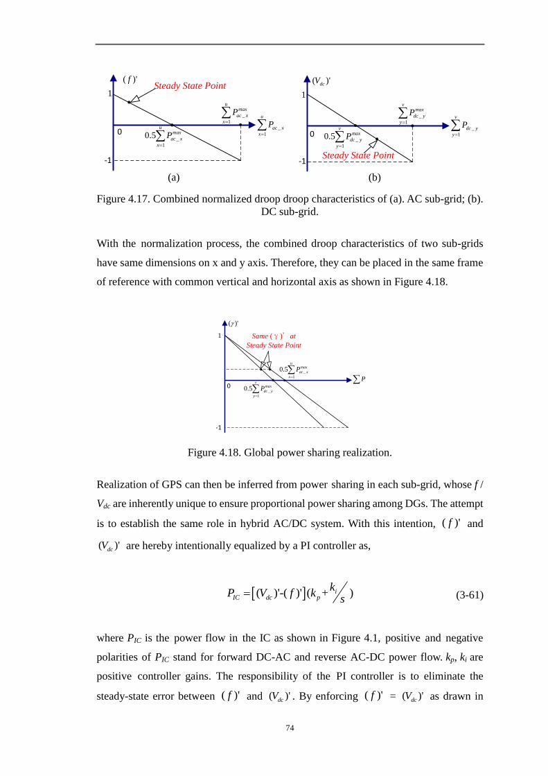
74
-1
1
_
1
u
ac x
x
P
_
1
umax
ac x
x
P
_
1
0.5u
max
ac x
x
P
( )'fSteady State Point
0
-1
1
_
1
v
dc y
y
P
_
1
vmax
dc y
y
P
_
1
0.5v
max
dc y
y
P
( )'dcV
Steady State Point
(b)
0
(a)
Figure 4.17. Combined normalized droop droop characteristics of (a). AC sub-grid; (b).
DC sub-grid.
With the normalization process, the combined droop characteristics of two sub-grids
have same dimensions on x and y axis. Therefore, they can be placed in the same frame
of reference with common vertical and horizontal axis as shown in Figure 4.18.
1
P
( )'
Same (γ)' at
Steady State Point
-1
_
1
0.5v
max
dc y
y
P
_
1
0.5u
max
ac x
x
P
0
Figure 4.18. Global power sharing realization.
Realization of GPS can then be inferred from power sharing in each sub-grid, whose f /
Vdc are inherently unique to ensure proportional power sharing among DGs. The attempt
is to establish the same role in hybrid AC/DC system. With this intention, ( )'f and
( )'dcV are hereby intentionally equalized by a PI controller as,
( )'-( )' ( + )iIC dc p
kP V f k
s (3-61)
where PIC is the power flow in the IC as shown in Figure 4.1, positive and negative
polarities of PIC stand for forward DC-AC and reverse AC-DC power flow. kp, ki are
positive controller gains. The responsibility of the PI controller is to eliminate the
steady-state error between ( )'f and ( )'dcV . By enforcing ( )'f = ( )'dcV as drawn in

75
Figure 18, it can be deduced from (4-43) and (4-44) that
__11
_ _
1 1
vu
dc yac xyx
u vnom nom
ac x dc y
x y
PP
P P
(3-62)
Combining (4-29), (4-34) and (4-46) follows that
___1 _ 2 _ 1 _1 _ 2 _1
_1 _ 2 _ _1 _ 2 __ _
1 1
= = = = = =
vu
dc yac xac ac ac u y dc dc dc vx
u vnom nom nom nom nom nomnom nomac ac ac u dc dc dc v
ac x dc y
x y
PPP P P P P P
P P P P P PP P
(3-63)
It is implied from (4-47) that, by exchanging the amount of power PIC between two
sub-grids, all DGs either in AC or DC sub-grid can share the entire load in proportion to
their nominal powers throughout the hybrid AC/DC system. The whole process of GPS
is also demonstrated in Figure 4.19.
Unit 1
Unit u
Unit 2
fmin
fmax
Pac_x
f
Pdc_y
d _1
max
cP _ 2
max
dcP _
max
dc vP
Vdc
min
dcV
max
dcVUnique Dc-bus Voltage
at Steady State Points
Combined AC Droop
Characteristics
fmin
fmax
f
Vdc
min
dcV
max
dcV
_
1
u
ac x
x
P
_
1
umax
ac x
x
P
_
1
v
dc y
y
P
_
1
vmax
dc y
y
P
Combined DC Droop
Characteristics
-1
1
_
1
u
ac x
x
P
_
1
umax
ac x
x
P
_
1
0.5u
max
ac x
x
P
( )'f
-1
1
_
1
v
dc y
y
P
_
1
vmax
dc y
y
P
_
1
0.5v
max
dc y
y
P
( )'dcV
Steady State Point
_1
max
acP
Steady State Point Unit 1 Unit 2 Unit v
Eqn. (4-45)
Enforces( )'=( )'dcf V
1
P
( )'
Same (γ)' at
Steady State Point
-1
_
1
0.5v
max
dc y
y
P
_
1
0.5u
max
ac x
x
P
(a)
(b)
(c)
(d)
(e)
(f)
(g)
0
0
0
_ 2
max
acP_
max
ac uP
Figure 4.19. Illustration of GPS principle: (a) & (b) individual droop characteristics; (c)
& (d) combined droop characteristics; (e) & (f) normalized combined droop
characteristics; (g) GPS realization.
To show how Figure 4.19 helps the IC to provide proper power tuning principle, four
cases can be tested, depending on the polarities of ( )'dcV and ( )'f . The following
documents the four cases.

76
(a) ( )' ( )'dcV f : According to Figure 4.19(e) and (f), this relative scenario means those
DGs in the AC sub-grid producing more power to meet its higher load demand than
those operating in the DC sub-grid with a comparably lower load demand. Excess
power therefore exists in the DC sub-grid, which can be transferred to the AC
sub-grid by the interfacing converter to meet its higher demand. The actual amount
of transferred power PIC is determined by (4-45), whose positive value matches to
power flowing from the DC to AC side.
(b) ( )' ( )'dcV f : On the contrast, when the variable ( )'f is much larger than ( )'dcV ,
which means those DGs in the DC sub-grid producing more power to meet its
higher load demand than those operating in the AC sub-grid according to Figure
4.19(e) and (f). Thus, excess power exists in the AC sub-grid, which can be
transferred to the DC sub-grid by the interfacing converter to meet its higher
demand. In this loading condition, the polarity of PIC becomes negetive which
indicates the power flow on the interfacing converter is from AC to DC side.
(c) ( )' ( )'>0dcV f : This scenario means that both the DC and AC sub-grids have
additional power capacities for the interfacing converter to absorb. Therefore, the
correct response expected from the interface should either be no or only tiny amount
of power flow, depending on how close ( )'f and ( )'dcV are. This outcome is
again correctly determined by (4-45), whose value is small and polarity depends on
the relative size of ( )'f and ( )'dcV .
(d) ( )' ( )'<0dcV f : This scenario means that both the DC and AC sub-grids are
overloaded and eager to absorb power from the interfacing converter. Therefore,
the correct response expected from the interface should either be no or only tiny
amount of power flow, depending on the difference between ( )'f and ( )'dcV .
Similarly, this outcome is again correctly determined by (4-45), whose value is
small and polarity depends on the relative size of ( )'f and ( )'dcV .
The principle of GPS has been explained in detail above. Based on GPS control, the
relevant control implementation applied to the IC is established in the following
sub-section.
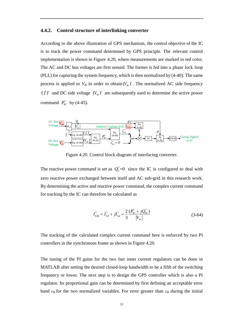
77
4.4.2. Control structure of interlinking converter
According to the above illustration of GPS mechanism, the control objective of the IC
is to track the power command determined by GPS principle. The relevant control
implementation is shown in Figure 4.20, where measurements are marked in red color.
The AC and DC bus voltages are first sensed. The former is fed into a phase lock loop
(PLL) for capturing the system frequency, which is then normalized by (4-40). The same
process is applied to Vdc in order to obtain ( )'dcV . The normalized AC side frequency
( )'f and DC side voltage ( )'dcV are subsequently used to determine the active power
command *
ICP by (4-45).
abcVPLL
acV
f
Eq. (4-40)dcV
ICP
abc
to dqLabci
0Lqi
Ldi
+-
PIdq
to abcPWM
Gating Signals
to IC
Eq. (4-40)Eq.
(4-45)
( )'f
( )'dcV
Eq.
(4-48)
AC Bus
Voltage
DC Bus
Voltage
Inductor Current of IC
Figure 4.20. Control block diagram of interfacing converter.
The reactive power command is set as *
2 =0Q since the IC is configured to deal with
zero reactive power exchanged between itself and AC sub-grid in this research work.
By determining the active and reactive power command, the complex current command
for tracking by the IC can therefore be calculated as
* *
* ** ( )2
3
ICLdq Ld Lq
IC
ac
P jQI
VI jI
(3-64)
The tracking of the calculated complex current command here is enforced by two PI
controllers in the synchronous frame as shown in Figure 4.20.
The tuning of the PI gains for the two fast inner current regulators can be done in
MATLAB after setting the desired closed-loop bandwidth to be a fifth of the switching
frequency or lower. The next step is to design the GPS controller which is also a PI
regulator. Its proportional gain can be determined by first defining an acceptable error
band εB for the two normalized variables. For error greater than εB during the initial

78
transient, the IC is designed to transfer its maximum active power PIC,max between the
sub-grids to rapidly bring down the transient error. The proportional gain acting on the
initial transient error can then be tuned as kp=2PIC,max / εB, where the factor of 2 is for
accounting bidirectional active power transfer. The transient error eventually
approaches to zero because of the integral term of GPS controller. Its corresponding
integral gain is set as ki=1000 to make it slower than the inner current regulator.
Moreover, a saturator is often placed after this GPS controller to limit the power flow on
the IC. GPS operation mode is hereby realized by stable and accurate tracking.
4.5. Simulation Results
For preliminary verification, the proposed GPS control for active power sharing
throughout entire hybrid AC/DC microgrid has been simulated with the autonomous
hybrid microgrid drawn in Figure 4.21. The power sharing among parallel DGs in any
single microgrid is not tested since the emphasis of this research work is to verify the
proposed GPS control scheme. Instead, parallel DG units dispersed in AC or DC
microgrid are represented by an equivalent DG unit with the combined droop
characteristics as expressed in (4-35) and (4-37), respectively.
+-
+-
+-
DC Microgrid AC Microgrid
Interlinking
Converter
DC Load
DC
Cable
AC Electronic
Load
AC
Cable
Figure 4.21. Test bed of hybrid AC/DC microgrid for global power sharing
verifications in both simulation and experiment.

79
Table 4.3. System parameters for both simulation and experiment.
Unit Parameters Simulation Experiment
AC
Sub-grid
f
50+1Hz 50+1Hz
acV
310+10V 80+10V
_1
nom
acP
5kW 1kW
_1
nom
acQ
3kVAr 1kVAr
DC
Sub-grid
dcV
700+20V 300+15V
_1
nom
dcP
6kW 1.2kW
GPS PI
Controller
ki 20000 20000
kp 1000 1000
System parameters for both simulation and experiment are listed in Table 4.3. For
simulation executions, the ratings of AC source is 5kW over a frequency range of
(49Hz, 51Hz), and 3kVAr over an AC voltage range of (300V, 320V). The
corresponding values for the DC microgrid are 6kW over a DC voltage range of (680V,
720V). Connecting them is a six-switch half-bridge DC-AC converter serving as the
IC. It is rated at 6kW and 3kVAr in total, allowing full active power exchange between
two sub-grids and reactive power exchange between AC sub-grid and the IC. Four
scenarios with respect to different loading conditions in both sub-grids are tested and
the simulation results are as shown in Figure 4.22. Four scenarios are organized as
follows.
Figure 4.22. Simulation results of the GPS controlled hybrid microgrid.

80
1) Scenario 1: light load in both sub-grids
The first event is related to light loading conditions in both sub-grids before t=2s. The
load in AC and DC sides are read as 0.27kW and 0.52kW, respectively, which can be
separately observed from the 2nd
and 4th
plots of Figure 4.22. The output power of DG
in AC sub-grid is read as 0.35kW as drawn in the 1st plot of Figure 4.22, while source
output from DC side is about 0.46kW as plotted in the 3rd
plot of Figure 4.22. For the
power generated from AC source, 0.27kW/0.35kW is consumed by the local AC load,
while the rest 0.08kW is enforced to be transferred to DC sub-grid through the
interlinking converter under GPS control. This is reflected by the power flow in the
interlinking converter, whose power flowing is read as -0.07kW from the 5th
plot of
Figure 4.22. The negative sign indicates that the direction of power flow is from AC to
DC sub-grid. The slight difference between the power exchanged from AC source to
DC sub-grid and the power flow in the interlinking converter is due to the losses due to
the switching action and transmission line. Although a small amount of power is
exchanged between two sub-grids, the effectiveness of global power sharing can still
be verified by the ratio from AC to DC output (0.35kW/0.46kW), which is
approximate proportional to their associated nominal values (5kW/6kW).
2) Scenario 2: light load in AC sub-grid and heavy load in DC sub-grid
The DC load step changes to 6.48kW at t=2s. The consumed power by the DC load
becomes extremely heavy and exceeds the rating of the DC source. In this instance, the
DC sub-grid will collapse if no power is pumped from AC sub-grid. This situation will
not happen in the GPS-controlled hybrid system as 2.8kW surplus power is pumped
from the AC sub-grid, supplying the overloaded DC load. By doing so, the AC source
is now generating 3.05kW, 0.27kW/3.05kW is consumed by local AC load and the rest
is transferred to the DC sub-grid. The output of DC source is about 3.7kW, which
means overloading operation for DC source is automatically avoided by GPS control.
Again, the accuracy of global power sharing can be verified by the ratio from AC to
DC output (3.05kW/3.7kW), which is quite close to the ration of their associated
nominal values (5kW/6kW).
3) Scenario 3: heavy load in both sub-grids
The AC load subsequently changes from 0.27kW to 3.6kW at t=4s. The loads in both
sub-grids become extremely heavy. It can be observed from Figure 4.22 that about

81
0.9kW power is transferred from AC sub-grid, supplying the overloaded DC load in
order to avoid collapse in the DC sub-grid. By doing so, the AC source is now
generating 4.5kW, 3.6kW/4.5kW is consumed by the local AC load and the rest
amount is transferred to the DC sub-grid. The output of the DC source is increased to
5.4kW, which results in a further voltage drop in DC bus. The further voltage drop in
DC bus cause a slight change in the DC load, which can be read as 6.3kW. Again, the
accuracy of global power sharing can be verified by the ratio from AC to DC output
(4.5kW/5.4kW), which is quite close to the ration of their associated nominal values
(5kW/6kW).
Table 4.4. Power flows of system components for different scenarios in simulation.
Scenarios System
Components
Power Flows
(kW)
1
Light DC
load
&
Light AC
load
DC load 0.52
AC load 0.27
DC source 0.46
AC source 0.35
Interfacing
converter -0.07
2
Heavy DC
load
&
Light AC
load
DC load 6.48
AC load 0.27
DC source 3.7
AC source 3.05
Interfacing
converter -2.8
3
Heavy DC
load
&
Heavy AC
load
DC load 6.3
AC load 3.6
DC source 5.4
AC source 4.5
Interfacing
converter -0.9
4
Light DC
load
&
Heavy AC
load
DC load 0.5
AC load 3.62
DC source 2.25
AC source 1.87
Interfacing
converter 1.74
4) Scenario 4: heavy load in AC sub-grid and light load in DC sub-grid
A step-down change finally happens in the DC load, whose value can be read as
changed from 6.3kW to 0.5kW at t=6s. The output of the DC source is now 2.25kW,
0.5kW/2.25kW is consumed by the local DC load and the rest is transferred to the AC
sub-grid. Note that the direction of power flow in the interlinking converter is reversed.
This can be indicated from the reversed sign of power flow. Referring to the AC load,

82
1.87kW/3,62kW is supplied by local AC source, while the rest is supplied by the
power transferred from DC side. Again, the accuracy of global power sharing can be
verified by the ratio from AC to DC output (1.87kW/2.25kW), which is quite close to
the ration of their associated nominal values (5kW/6kW).
Given that the vague readability of the power values in Figure 4.22, the relevant power
values in different scenarios are listed in Table 4.4 for transparency in simulation
results.
4.6. Experiment Verifications
For verifying the practicality of the proposed scheme, a scaled-down hybrid system
based on the layout in Figure 4.21 is built in the laboratory. As understood from the
above simulated plots, a large amount of waveforms is needed to be captured, which in
practice might not be possible because of the limited channels of digital scopes.
Therefore, the calculated output power of VSI and AC system frequency are plotted in
DSpace/Controldesk. The other variables for observation are captured in two sets of
oscilloscopes.
For experiment implementation, the AC sub-grid is rated at 1kW over a frequency
range of (49Hz, 51Hz). The corresponding values for the DC microgrid are 1.2kW
over a DC voltage range of (285V, 315V). Two transient events in terms of different
directions of power flow on IC are carried out as follows.
1) Power flow from AC to DC sub-grid
Initial state (before t=1s):
The loads in AC and DC sub-grids are initially set as 280W and 400W as shown in
Figure 4.33(c)-C5 and Figure 4.33(d)-C6, respectively, while sources in AC and DC
sub-grids are generating approximate 300W and 410W as shown in Figure 4.33(a) and
Figure 4.33(d)-C5, respectively. The AC side frequency can be read as 50.3Hz from
Figure 4.33(b) and DC bus voltage is read about 305V from Figure 4.33(d)-C4. Since
the normalized AC side frequency and DC bus voltage are quite close, a very small
amount of power is flowing through the interlinking converter according to the GPS
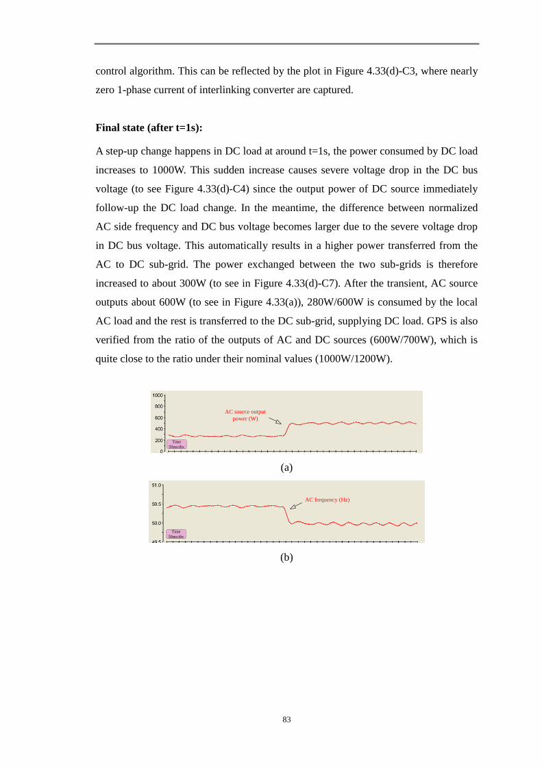
83
control algorithm. This can be reflected by the plot in Figure 4.33(d)-C3, where nearly
zero 1-phase current of interlinking converter are captured.
Final state (after t=1s):
A step-up change happens in DC load at around t=1s, the power consumed by DC load
increases to 1000W. This sudden increase causes severe voltage drop in the DC bus
voltage (to see Figure 4.33(d)-C4) since the output power of DC source immediately
follow-up the DC load change. In the meantime, the difference between normalized
AC side frequency and DC bus voltage becomes larger due to the severe voltage drop
in DC bus voltage. This automatically results in a higher power transferred from the
AC to DC sub-grid. The power exchanged between the two sub-grids is therefore
increased to about 300W (to see in Figure 4.33(d)-C7). After the transient, AC source
outputs about 600W (to see in Figure 4.33(a)), 280W/600W is consumed by the local
AC load and the rest is transferred to the DC sub-grid, supplying DC load. GPS is also
verified from the ratio of the outputs of AC and DC sources (600W/700W), which is
quite close to the ratio under their nominal values (1000W/1200W).
Time
50ms/div
AC source output
power (W)
(a)
Time
50ms/div
AC frequency (Hz)
(b)

84
C5
C1
C3
C5: AC load (200W/div)
C1&C2: 2-phase AC load current (2A/div)
C3&C4: 2-phase AC bus voltage (100V/div)
Time
200ms/div
C2
C4
(c)
Time
200ms/div
C4
C1
C2
C3
C5
C6
C7
C3: 1-phase current on IC (2A/div)
C7: exchanged power (500W/div)
C4: DC bus voltage (200V/div)
C1: DC source current (2A/div)
C2: DC load current (2A/div)
C5: DC source output power (500W/div)
C6: DC load (500W/div)
(d)
Figure 4.23. Experimental AC and DC waveforms in transient event 1: (a) output
power of AC source; (b) AC system frequency; (c) AC load; (d) DC source output, DC
load and power flow on interlinking converter.
2) Power flow from AC to DC sub-grid
Initial state (before t=1s):
In this case, the loads in the AC and DC sub-grids are initially configured as 350W and
120W as shown in Figure 4.34(c)-C5 and Figure 4.34(d)-C6, respectively, while the
sources in AC and DC sub-grids are generating approximately 220W and 280W as
shown in Figure 4.33(a) and Figure 4.33(d)-C5, respectively. The AC side frequency
can be read as 50.65Hz from Figure 4.33(b) and the DC bus voltage is read about
312V from Figure 4.33(d)-C4. Since the normalized AC side frequency is slightly less

85
than normalized DC bus, a very small amount of power (150W) is flowing from the
DC to AC sub-grid according to the GPS control algorithm. This can be reflected by
the plot in Figure 4.33(d)-C7, whose positive sign denotes forward DC-AC power flow.
Although a small amount of power is generated from sources in both sub-grids, the
effectiveness of GPS can also be verified from the ratio of the outputs of AC and DC
sources (220W/280W), which is quite close to the ratio under their nominal values
(1000W/1200W). Note that the errors between those two ratios are mainly due to the
power losses due to the switching actions and transmission line.
Final state (after t=1s):
At around t=1s, a step-up change happens in the AC load, the power consumed by the
AC load increases to 800W as explicated in Figure 4.33(c)-C5. This sudden increase
causes a further frequency drop in AC system (to see Figure 4.33(b)) since the output
power of AC source immediately follow-up with the AC load increase. In the
meantime, the difference between the normalized AC side frequency and DC bus
voltage become even larger due to the further voltage drop in the AC system frequency.
This would automatically results in a higher power transferred from the DC to AC
sub-grid. The power exchanged between the two sub-grids is therefore increased to
about 360W (to see in Figure 4.33(d)-C7).
After the transient, the AC source output can be read as 450W (to see in Figure
4.33(a)), while the output of DC source is 500W. For this amount of power from DC
source, 120W/500W is consumed by the local DC load and the rest is transferred to the
AC sub-grid, supplying AC load. After the transients, the effectiveness of GPS is
alsocollectively verified by the ratio of the outputs of AC and DC sources
(450W/500W), which is quite close to the ratio under their nominal values
(1000W/1200W).
Time
50ms/div
AC source output
power (W)
(a)

86
Time
50ms/div
AC frequency (Hz)
(b)
C5
C5: AC load (200W/div)
C1&C2: 2-phase AC load current (2A/div)
C3&C4: 2-phase AC bus voltage (100V/div)
Time
200ms/div
C1
C2
C3
C4
(c)
Time
200ms/div
C4
C1
C2
C3
C5
C6
C7
C3: 1-phase current on IC (2A/div)
C7: exchanged power (500W/div)
C4: DC bus voltage (200V/div)
C1: DC source current (2A/div)
C2: DC load current (2A/div)
C5: DC source output power (500W/div)
C6: DC load (500W/div)
(d)
Figure 4.24. Experimental AC and DC waveforms in transient event 2: (a) output
power of AC source; (b) AC system frequency; (c) AC load; (d) DC source output, DC
load and power flow on interlinking converter.
For completeness experimental illustrations, the power flows in different states for two
cases are listed in Table 4.5. The experiment results shows that, through normalization
AC frequency and DC bus voltage, the proposed GPS control scheme can
automatically manage the power balance within each sub-grid as well as the power
exchange between two sub-grids.

87
Table 4.5. Power flows of system components for different scenarios in experiment.
Scenarios Initial state Final state
System
Components
Power Flows
(W)
System
Components
Power Flows
(W)
Power flow
direction on IC:
AC microgrid
↓ DC microgrid
DC load 400 DC load 1000
AC load 280 AC load 280
DC source 410 DC source 700
AC source 300 AC source 600
Interfacing converter
0 Interfacing converter
-300
Power flow direction on
IC:
DC microgrid ↓
AC microgrid
DC load 120 DC load 120
AC load 350 AC load 800
DC source 280 DC source 500
AC source 220 AC source 450
Interfacing
converter 150
Interfacing
converter 360
4.7. Conclusions
This chapter presents a GPS control for power distributed in an autonomous hybrid
AC/DC microgrid. Droop control and its improved variants for DGs in individual AC
or DC sub-grid have been reviewed first. The power sharing among DGs in single
microgrid is then established. A normalization technique is adopted to normalize
information on both sides of the IC before an appropriate power flow command is well
tuned. With the normalization method, the principle of GPS is subsequently interpreted
by means of mathematical and graphical methods. Different operation scenarios have
been preliminarily verified in simulations and eventually tested in experimental results
in order to verify the effectiveness of proposed control scheme. The rule of GPS
provides an effective fully decentralized control scheme for reliable autonomous
operation of the hybrid system.

88
Chapter 5 Distributed Control for Autonomous Operation
of Hybrid AC/DC/DS Microgrids
5.1. Introduction
Global power sharing (GPS) for autonomous operation of hybrid AC/DC microgrids
has been introduced in the last chapter without considering the operations of
distributed storages (DSs). In fact, the hybrid microgrid can hardly be fully autonomous
without DSs for energy buffering, power balancing and fault riding-through if the
impacts of variable random loads at the demand end and intermittent renewable sources
at the supply end are considered. With the consideration of integrating DSs into hybrid
AC/DC system, a three-bus AC/DC/DS hybrid infrastructure is proposed in this
chapter. In this layout, DGs and DSs with the same type are placed together in the
relevant AC, DC or DS bus in order to avoid the complexity of power management and
enforce coincident control scheme to DGs and DSs. For managing the power flow and
maintaining reliable operation of such a complex hybrid system, a distributed control
including a fully decentralized control for independent DG (or DS) control and a
multilevel power exchange control for optimal fashion improvement will be elaborated
in the following sections.
5.2. Proposed Hybrid AC/DC/DS Structure
The storages which are configured to behave in different manners for specific microgrid
applications have been investigated in many publications [16, 61, 83, 86]. In [16, 61],
the storage units are controlled as a voltage source in a DC microgrid, coordinately
regulating the DC bus voltage with the renewable and conventional sources. On the
other hand, the storages are capable of serving as a current source in an AC microgrid,
absorbing/releasing the surplus power from/to the generation supply/load demand in an
automated manner [83, 86]. In this sense, different control schemes for DS will
undoubtedly increase the complexity of power management in hybrid AC/DC microgrid
with storages in spite of DS locations in the AC or DC sub-grid. Therefore, fulfilling the
requirement of “plug-and-play” is getting difficult since all DS dispersed in the hybrid
AC/DC system are not controlled in a coincident way.

89
To avoid the complexity of power management and enforce coincident control scheme
to DS, a hybrid microgrid scenario with three-bus including the AC, DC, and DS buses
is proposed as shown in Figure 5.1. In this layout, the DS units are intensively tied to the
DS bus whilst the DGs are connected to associated AC or DC bus according to their
electrical properties and geographical locations. In this sense, sources, storages and
loads of the same type are placed together to avoid control complexity and minimize the
losses in multi-stage power conversions. With such a hybrid system established, the
companied challenges are to find applicable interconnections to link up three networks
and develop proper control scheme to maintain the power balance within individual
network and manage the power exchange amongst three networks.
Figure 5.1. Overview of the architecture of hybrid AC/DC/DS microgrid.
For detailed implementation, the overall system configuration of the proposed hybrid
AC/DC/DS system is shown in Figure 5.2. It comprises of an AC bus, a DC bus, and a
DS bus. As shown in Figure 5.2, u and v DG units are connected to the AC and DC buses,
respectively. The AC and DC buses are interconnected by a two-stage interlinking
converter (IC) whose intermediate DC-link is treated as the DS bus. The DS bus is
connected by w DS units. An intelligent transfer switch is tying the AC network to the
grid, allowing the entire system to operate in both grid-connected and islanded modes.
In terms of active power dispatch, a DG unit can be categorized as a dispatchable or
non-dispatchable unit [87]. Examples of dispatchable DGs include micro-turbines and
fuel cells, which are in charge of regulating system voltage and frequency during
islanded operations by means of producing controlled active power on demand. On the
contrary, non-dispatchable DGs like solar and wind generations whose output are solely
dependent on weather conditions usually operate at their maximum power points in
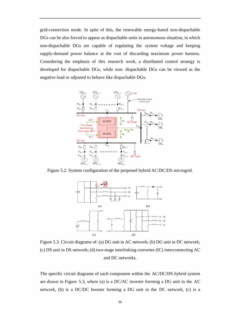
90
grid-connection mode. In spite of this, the renewable energy-based non-dispachable
DGs can be also forced to appear as dispachable units in autonomous situation, in which
non-dispachable DGs are capable of regulating the system voltage and keeping
supply-demand power balance at the cost of discarding maximum power harness.
Considering the emphasis of this research work, a distributed control strategy is
developed for dispachable DGs, while non- dispachable DGs can be viewed as the
negative load or adjusted to behave like dispachable DGs.
Figure 5.2. System configuration of the proposed hybrid AC/DC/DS microgrid.
Figure 5.3. Circuit diagrams of: (a) DG unit in AC network; (b) DG unit in DC network;
(c) DS unit in DS network; (d) two-stage interlinking converter (IC) interconnecting AC
and DC networks.
The specific circuit diagrams of each component within the AC/DC/DS hybrid system
are drawn in Figure 5.3, where (a) is a DC/AC inverter forming a DG unit in the AC
network, (b) is a DC/DC booster forming a DG unit in the DC network, (c) is a

91
bidirectional DC/DC converter representing a DS unit in the DS network, and (d) is the
two-stage IC, including both bidirectional DC/DC (IC1) and DC/AC converters (IC2).
The IC ties three networks together, allowing bidirectional power flow at all buses. The
difficulty is then to develop a distributed coordination control for maintaining power
balance in each individual network and managing power exchange among three
networks. This is realized by the proposed distributed control illustrated in detail as
follows.
5.3. Proposed Distributed Control
So far, reliable and economical operations of such a complex three-port AC/DC/DS
system usually involve multi-layer supervision system and advanced energy
management algorithm, which rely heavily on a high-speed communication path for
coordination control of fast-switched converters [88-92]. This may obviously degrade
the system redundancy in addition to result in system outage during the malfunction in
the communication carrier. Decentralized control promises a solution to enhance the
system redundancy since each unit is controlled using local measurements without
communication links [93]. From this viewpoint, it provides an alternative way of riding
through communication multifunction.
As introduced in previous chapters, the droop control method has been well-prove to
implement decentralized control to DGs within microgrid. Authors in [54] propose a
three-level hierarchical control, in which, the primary control for power sharing, the
secondary control for frequency/voltage recovery, and the tertiary control for power
dispatching are applied to individual AC or DC microgrids so as to imitate the primary
frequency/voltage regulation, secondary frequency/voltage recovery, and power
dispatch control in conventional power system, respectively. However, only the
individual network’s power balance is decentralized in the primary control by using the
droop control method. The fully decentralized control for the entire hybrid system
operation, including power balance within individual networks and power exchange
amongst AC and DC networks, is not taken into account.
The GPS control described in the last chapter offers a alternative way to realize a fully
decentralized controlled hybrid AC/DC system. However, the unconstrained GPS

92
control is implemented consistently, which results in additional power loss due to the
unnecessary power exchange behaviors. Moreover, by modifying the interconnection
topology from a single power stage to the dual, the proposed decentralized control in
[83] is also extended to include energy storage within the interconnection converters.
However, power sharing amongst multiple DSs with regard to relevant storage capacity
and state-of-charge (SoC) is still not considered.
Figure 5.4. Illustration of the proposed distributed control for hybrid AC/DC/DS
microgrid.
To cope with the aforementioned problems, a distributed control strategy for
autonomous operation of three-bus AC/DC/DS hybrid microgrid is proposed in this
chapter for enabling large-scale integration of DGs and DSs into future networks. The
proposed distributed control can be illustrated with the help of Figure 5.4. It includes a
fully decentralized control and a multi-level power exchange control. For the former, it
comprises of: (1) source droop control for local power sharing (LPS) within individual
AC or DC network; (2) GPS control for global power sharing throughout entire AC and
DC networks; (3) demand droop control for storage power sharing (SPS) among DS
units. For the multi-level power exchange control, it is employed to schedule the
activation sequences among LPS, GPS and SPS so as to restrain unnecessary GPS
behaviors and reduce the usage of DS. Since LPS and GPS for DGs and the interlinking
converter (IC) are well explained in Chapter 4, it is not introduced in this chapter. Note

93
that for two-stage IC in this system, GPS control is implemented on the bidirectional
DC/AC converter (IC2 as shown in Figure 5.2), while the bidirectional DC/DC
converter (IC1 as shown in Figure 5.2) is responsible for maintaining the intermediate
DC-link voltage.
5.4. Storage Power Sharing for DS Units
By realizing LPS and GPS in previous chapter, global supply-demand conditions
(GSDC) throughout two sub-networks are linkup. AC and DC networks are expected to
operate around the nominal f/Vdc. Higher/lower f (or Vdc) indicates relatively
lower/higher loading condition with respect to entire generation capacities. This would
lead to unexpected f/Vdc deviations which are inherent accompaniments with LPS. To
limit those deviations, the operation criteria of DS units can be clarified by monitoring
GSDC as follows:
a) Charging mode: DS units would absorb surplus power from DGs if total loads are
light, and 0< ( )'f = ( )'dcV <1.
b) Discharging mode: DS units would releases power to system if total loads are heavy
and -1< ( )'f = ( )'dcV <0.
The GSDC is measured by the average loading condition of AC and DC networks as:
( )' ( )'
2
dcf V
(3-65)
Similar to DC voltage and AC frequency, who perform the role for ensure LPS among
DGs by source droop control, the index ζ can be inferred to play the same role for
ensuring SPS in DS network by demand droop control as:
_z ds zb P (3-66)
where bipolar variable Pds_z is absorbed/released power of zth
DS unit, its positive value
denotes discharge and vice versa. bz is the negatively droop coefficient of zth
DS as

94
shown in Figure 5.5, and it is designed as
_
1maxz
ds z
bP
(3-67)
Unit 1 Unit 2 Unit w
1
Pds_z_1
max
dsP
_1
max
dcP
_ 2
max
dsP
_ 2
max
dsP
_
max
ds wP
_
max
ds wP
-1
Unique ζ
Ensure SPS
0
Figure 5.5. Capacity-based demand droop for SPS among DSs in DS network.
Based on the equal , all DSs proportionally absorb/release power based on their
capacities,
_1 _ 2 _
_1 _ 2 _
= = =ds ds ds w
max max max
ds ds ds w
P P P
P P P (3-68)
Upon establishment of demand droop controlled DS units, the differences between
source droop control and demand droop control can be summarized as follows:
a) For conventional source droop control, it generally droops the AC system
frequency or DC bus voltage by the measured output powers of DGs. The DG
therefore essentially performs in voltage controlled mode.
b) For demand droop control, it droops the absorb/release powers of DSs by
measured GSDC. In fact, it is the reverse process of source droop control. The
demand droop controlled DS therefore can be viewed as a current controlled
source.
In practice, storage capacity and charging rate vary with state of charge (SoC) in system
operation. Considering this effect in SPS, a SoC-based droop coefficient 'zb is
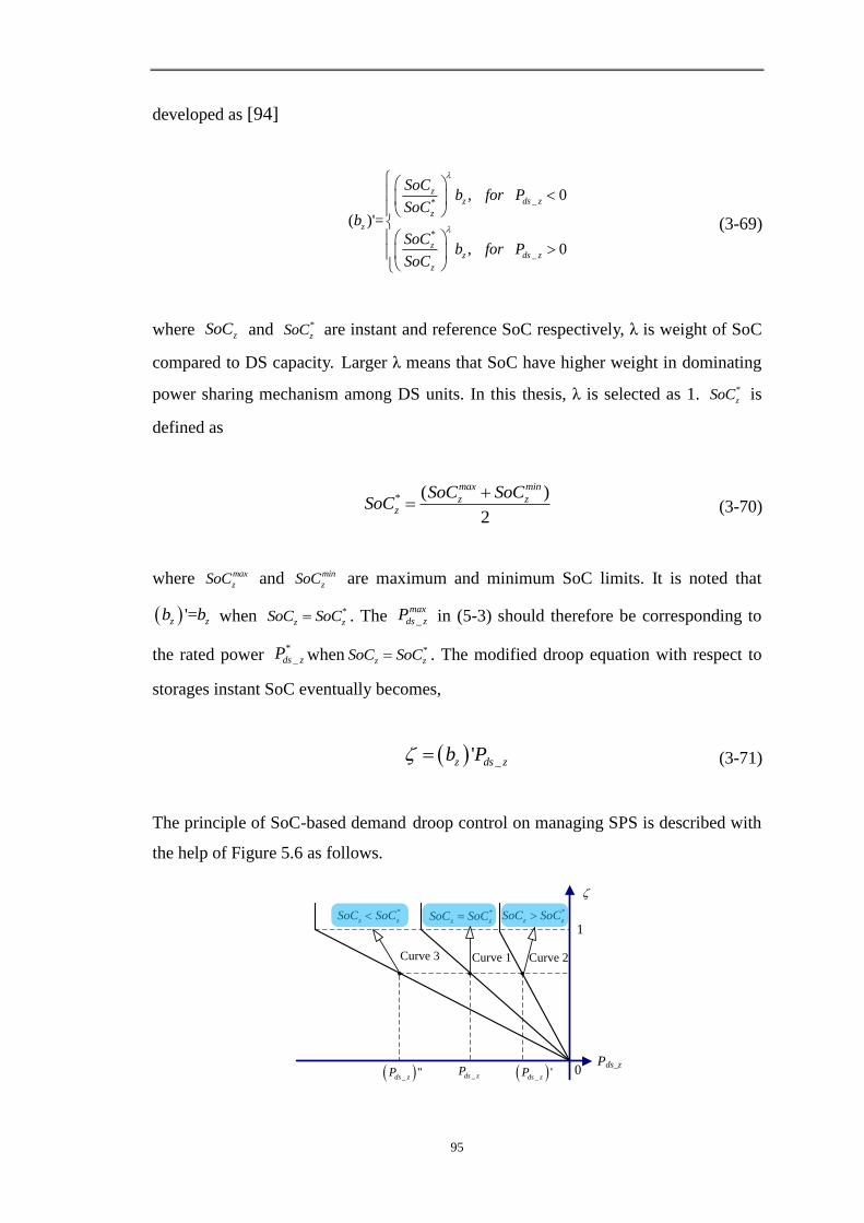
95
developed as [94]
_*
*
_
, 0
( )'=
, 0
zz ds z
z
z
zz ds z
z
SoCb for P
SoCb
SoCb for P
SoC
(3-69)
where zSoC and *
zSoC are instant and reference SoC respectively, λ is weight of SoC
compared to DS capacity. Larger λ means that SoC have higher weight in dominating
power sharing mechanism among DS units. In this thesis, λ is selected as 1. *
zSoC is
defined as
* ( )
2
max min
z zz
SoC SoCSoC
(3-70)
where max
zSoC and min
zSoC are maximum and minimum SoC limits. It is noted that
'=z zb b when *
z zSoC SoC . The _
max
ds zP in (5-3) should therefore be corresponding to
the rated power *
_ds zP when *
z zSoC SoC . The modified droop equation with respect to
storages instant SoC eventually becomes,
_'z ds zb P (3-71)
The principle of SoC-based demand droop control on managing SPS is described with
the help of Figure 5.6 as follows.
Pds_z
_ds zP
0
1
*
z zSoC SoC*
z zSoC SoC*
z zSoC SoC
_ 'ds zP _ ''ds zP
Curve 1 Curve 2Curve 3
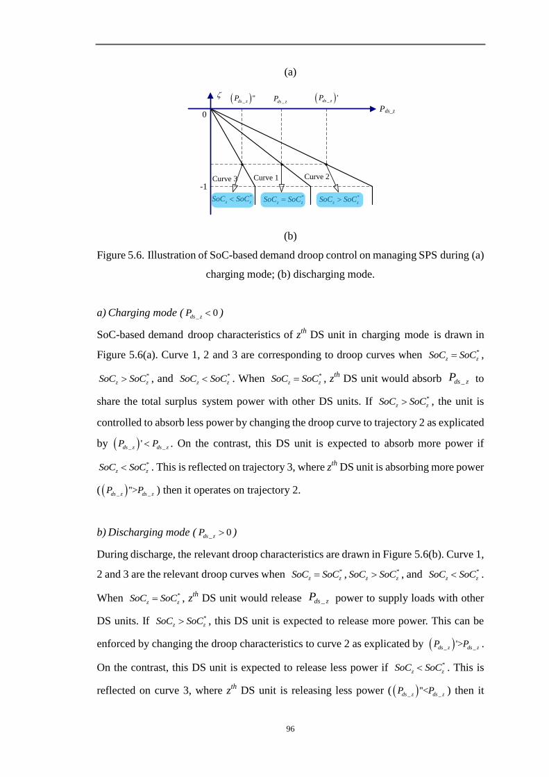
96
(a)
-1
Pds_z0
_ds zP _ 'ds zP _ ''ds zP
*
z zSoC SoC *
z zSoC SoC*
z zSoC SoC
Curve 1 Curve 2Curve 3
(b)
Figure 5.6. Illustration of SoC-based demand droop control on managing SPS during (a)
charging mode; (b) discharging mode.
a) Charging mode ( _ 0ds zP )
SoC-based demand droop characteristics of zth
DS unit in charging mode is drawn in
Figure 5.6(a). Curve 1, 2 and 3 are corresponding to droop curves when *
z zSoC SoC ,
*
z zSoC SoC , and *
z zSoC SoC . When *
z zSoC SoC , zth
DS unit would absorb _ds zP to
share the total surplus system power with other DS units. If *
z zSoC SoC , the unit is
controlled to absorb less power by changing the droop curve to trajectory 2 as explicated
by _ _'ds z ds zP P . On the contrast, this DS unit is expected to absorb more power if
*
z zSoC SoC . This is reflected on trajectory 3, where zth
DS unit is absorbing more power
( _ _''>ds z ds zP P ) then it operates on trajectory 2.
b) Discharging mode ( _ 0ds zP )
During discharge, the relevant droop characteristics are drawn in Figure 5.6(b). Curve 1,
2 and 3 are the relevant droop curves when *
z zSoC SoC , *
z zSoC SoC , and *
z zSoC SoC .
When *
z zSoC SoC , zth
DS unit would release _ds zP power to supply loads with other
DS units. If *
z zSoC SoC , this DS unit is expected to release more power. This can be
enforced by changing the droop characteristics to curve 2 as explicated by _ _'>ds z ds zP P .
On the contrast, this DS unit is expected to release less power if *
z zSoC SoC . This is
reflected on curve 3, where zth
DS unit is releasing less power ( _ _''<ds z ds zP P ) then it

97
operates on curve 2.
By introducing SoC-based demand droop control, power sharing among storages can be
realized according to their respective capacity and SoC.
5.5. Multi-level Power Exchange Control
Based on the three power sharing methods — LPS, GPS and SPS, the fully
decentralized power management for the hybrid microgrid can be realized. Nevertheless,
consistent operation of GPS and SPS under all operating conditions is not economic. On
the one hand, unnecessary GPS operation will result in considerable power losses in the
IC and cables when both the AC and DC sides are locally balanced. On the other hand,
frequent charge/discharge of DSs with load variation under the SPS scheme may lead to
obvious degradation of battery life. Therefore, a multi-level power exchange control
scheme is proposed to restrain unnecessary GPS and SPS operations.
Under the proposed scheme, the tolerance band of the normalized f/Vdc is divided into
three regions by two threshold values ( )'g
and ( )'s
for scheduling and prioritizing
the activation sequences of LPS, GPS and SPS ( denotes f or Vdc).
1: ( )' ( )'
2 : ( )' ( )' ( )'
3 : ( )' ( )' 1
g
g s
s
Region
Region
Region
(3-72)
a) In Region 1, power is locally balanced in both AC and DC sides under the system
limits. The AC frequency and DC voltage are around their nominal values. Only
LPS is executed in the AC and DC networks. GPS and SPS operations are not
activated.
b) In Region 2, at least one of f or Vdc exceeds the threshold value ( )'g
, which
indicates large deviations in AC frequency or DC voltage. GPS is therefore
activated to avoid too large deviation in any single network.
c) In Region 3, the frequency and voltage deviations are close to system limitation
values, SPS operation is triggered to prevent the system from operating over/under

98
frequency/voltage.
By clarifying the schedule sequences of LPS, GPS and SPS, the multi-level power
exchange control can be demonstrated as shown in Figure 5.7. Details on the logical
operation of scheduling GPS and SPS are described below.
GPS
Region 1
LPS
SPS
Region 3Region 2
Figure 5.7. Illustration of multi-level power exchange control.
5.5.1. Scheduling of global power sharing (GPS) operation
The GPS should be triggered as long as ( )' ( )'g
. However, the condition of
disabling GPS is not as straightforward as ( )' ( )'g
for some operating conditions,
which may lead to malfunction of GPS disabling. For example, power flow under the
condition of heavy AC and light DC loads is from DC to AC during LPS+GPS operation
mode. In this case, the GPS should have been disabled when the normalized f or Vdc
satisfy | ( )'|=|( )'| ( )'dc gf V . After GPS is disabled, the large deviations ( )'f and ( )'dcV
under LPS may lead to ( )' ( )'g
and GPS re-triggering. The system becomes
unstable due to the switching between LPS mode and LPS+GPS mode.
Therefore ( )' ( )'g
cannot be directly used as the consistent condition for GPS
scheduling. A uniform condition is developed to schedule GPS. Based on frequency
change f and voltage change dcV when the system transfers from LPS to LPS+GPS,
two condition events A and B are defined as

99
Event A: ( )' ( )'f gf f (3-73)
Event B: ( )' ( )'dcdc V dc g
V V (3-74)
where f and dcV can be obtained from (4-35) and (4-37).
Before GPS is triggered, f and dcV are zero because of no power exchange between
two sub-networks (P1=P2=0). Events A and B become ( )' ( )'g
f f and
( )' ( )'dc dc gV V , which intuitively indicates that GPS will be triggered once
( )' ( )'g
.
During LPS+GPS operation, ( )'ff and ( )'dcdc VV are updated online. If both
Event A and B become false, GPS operation can be disabled. The original GPS
expression in (4-45) can thus be modified as
2
( )' ( )' ( + ), 1
0, 0
idc p
kf V k A B
sP
A B
(3-75)
where is the logical “OR” operator.
5.5.2. Scheduling of storage power sharing (SPS) operation
Inferred from the scheduling of GPS, the scheduling criteria of SPS can be obtained by
modifying (5-7) as
_
, 1'
0, 0
zds z
CbP
C
(3-76)
where 0.5 ( )' ( )' ( )'dcf dc V s
f V is labeled as logical Event C. By

100
summarizing the scheduling principle of GPS and SPS, the logical relationships about
mode change among LPS, GPS, and SPS is demonstrated in Figure 5.8.
Figure 5.8. Conditions and associated mode switching of LPS, GPS, and SPS.
5.6. Simulation Results
For preliminary verification, Matlab/Simulink simulation is first executed with the
proposed distributed control scheme applied to the hybrid AC/DC/DS microgrid
prototype as shown in Figure 5.9. Since power sharing method in individual AC or DC
network has been well-verified in the literature, LPS among parallel DGs is not
considered in simulation and experiment. Therefore, only one DG unit is placed in each
network as shown in Figure 5.9 in order to reduce complexity. Relevant system
parameters for simulation and experiment verifications are both listed in Table 5.1. Five
cases are first simulated as follows and the results are shown in Figure 5.10.

101
+-
+-
+-
DC Network AC Network
Interlinking
Converter
DC Load
DC
Cable
Lead-acid
Batteries
Lithium
Batteries
AC Electronic
Load
AC
Cable
Distributed
Storage 1
Distributed
Storage 2
Figure 5.9. Test bed of the proposed hybrid AC/DC/DS system.
Table 5.1. System Parameters for Simulation and Experiment Verifications.
Unit Parameters Simulation Experiment
AC
Network
f 50Hz+2% 50Hz+2%
acV
310+10V 90+10V
_1
nom
acP
6000W 1200W
_1
max
acQ
3000W 1000W
( )'g
f
0.2 0.2
( )'s
f
0.6 0.8
DC
Network
dcV 380+20V 300+15V
_1
nom
dcP
5000W 1500W
dc( )'g
V
0.2 0.2
dc( )'s
V
0.6 0.8
DS
Network
_1dsV 300V 200V
_ 2dsV 200V 100V
_1 _1&max min
ds dsP P
+3000W +1000W
_2 _2&max min
ds dsP P
+2000W +800W
1SoC 30% 30%
2SoC 70% 70% *SoC 50% 50%
Other Vm 700V 400V
Case 1: The AC and DC loads are initially set to 2.87kW and 2.40kW respectively.
( )'ff and ( )'dcdc VV are 0.05 and 0.04 respectively. Therefore Events A and B are
not true. There is no power exchange among three networks. DGs in AC and DC

102
networks are now supplying 2.88kW and 2.43kW to their local loads, respectively.
0
1
2
3
4
5
6
7
0
1
2
3
4
5
6
-6
-4
-2
0
2
-2
0
2
4
6
-2
0
2
4
6
0 2 4 6 8 10-3
-2
-1
0
1
2
3
0 2 4 6 8 10-1
-0.5
0
0.5
1
State 1 State 2 State 3 State 4 State 5A
C n
etw
ork
acti
ve
po
wer
(k
W)
DC
net
wo
rk p
ow
er (
kW
)P
ow
er f
low
on
IC
(k
W)
and
Ev
ent
A&
B m
on
ito
rin
g
DS
net
wo
rk p
ow
er (
kW
)
and
Ev
ent
C m
on
ito
rin
g
Time (s)
Load
Source
Source
Load
IC1
IC2
|(Vdc-ΔVdc)'|
|(f+Δf)'|
Pds_1
Pds_2
0.5[(f+Δf)'+(Vdc-ΔVdc)']
Sub-state
Sub-state
Sub-state
Sub-state
Figure 5.10. Simulated active power flows on source, storage and interlinking
converters.
103
Case 2: When the DC load changes from 2.4kW to 4.57kW at t=2s, ( )'dcdc VV is
about 0.82. True Event B enables GPS operation. In GPS mode, AC source supplies
4.05kW. For this amount of power, 2.87 kW/4.05kW is for the AC load and the rest is
transferred to supply the DC load. The DC source supplies the rest of the DC load which
is around 3.41kW. It is obvious that the AC and DC sources can share the entire load in
proportion to their ratings 6kW, 5kW. Since Event C is false, there is no power
exchange between DS and others.
Case 3: When the AC load suddenly changes from 2.87kW to 5.72kW at t=4s, both the
AC and DC loads are heavy and 0.5 ( )' ( )'dcf dc Vf V is about -0.9. True Event C
activates SPS. DS1 and DS2 generate 0.85kW and 1.33kW respectively. DS1 with a
higher capacity generates less power than DS2. The reason is that the SoC of DS1 is
lower than that of DS2 at this intant. The effect of SoC-based demand droop control for
SPS is verified in this case. 0.85kW of the total power from DS network is transferred to
the DC network and1.33kW is transferred to AC network. The AC and DC sources
generate 4.40kW and 3.69kW respectively, in proportion to their power ratings.
Case 4: When the AC load changes from 5.72kW to 0.29kW at t=6s, the overall system
loading condition is normal. ( )'ff and ( )'dcdc VV are 0.9 and -0.91 respectively.
Both Event A and B remain true. The system is in GPS operation mode. AC and DC
sources are now generating 2.75kW and 2.33kW respectively, which are proportional to
their power ratings. Although ( )'ff and ( )'dcdc VV are beyond their limited
thresholds, the entire loading condition is not too heavy or too light. This causes Event C
to be false. Therefore, the power exchange on DS bus returns to zero.
Case 5: When the DC load changes from 4.57kW to 0.31kW at t=8s, loads in both sides
become light. At this instant, 0.5 ( )' ( )'dcf dc Vf V reaches to 0.9. True Event C
activates SPS again. DS1 and DS2 then absorb 2.05kW and 0.58kW surplus power from
the DGs. It is noted that, the ratio of absorbed powers 2.05/0.58 is higher than their
ratings ratio 3/2. The reason for this is that the instantaneous SoC of DS1 is lower than
that of DS2. It should absorb more power in charging mode. The effect of SoC-based
droop characteristics for SPS is also verified in this case. Of the gross stored power from

104
DGs, 1.18kW is from the DC network via IC1, while 1.47kW is from the AC network
via IC2. Proportional power sharing throughout AC and DC network can be inferred
from 1.75kW output from the AC source and 1.48kW output from the DC source.
5.7. Experiment Verifications
For verifying the proposed distributed control scheme practically, a scaled-down
experimental prototype as shown in Figure 5.9 was built up in the laboratory. Since the
number of monitored waveforms was enormous for full observation, some variables
were displayed in DSpace/ControlDesk, while others were displayed on oscilloscopes.
Relevant experimental parameters are listed in Table 5.1. The AC network is formed by
a droop controlled DC-AC inverter, rated at 1200W with a frequency range of 49Hz < f
< 51Hz. The DC network is realized by a droop-controlled booster with a rating of
1500W and a voltage range of 285V < Vdc < 315V. On the DS side, a lead-acid battery
bank with a rated voltage of 200V and a lithium battery bank with a rated voltage of
100V are connected to the DS bus via battery converters. Their instantaneous SoC were
preset as 30% and 70%, respectively, while the rated stored/released power of two
storage elements are +1000W and +800W, respectively. Two experimental cases were
executed, including (1) transient behavior from LPS to LPS+GPS; (2) transient behavior
from LPS+GPS to LPS+GPS+SPS. The respective results are shown in Figure 5.11 and
5.12 as below.
Case 1: LPS → LPS+GPS
Figure 5.11 shows the network transients when the system changes the operation mode
from LPS to LPS+GPS.
Initial State (before t=1s): The AC load is 600W (C5 in Figure 5.11(c)) and the DC load
is about 650W (C6 in Figure 5.11(d)). The outputs of the AC and DC sources are around
600W (Figure 5.11(a)) and 650W (shown in Figure 5.11(d)-C5), respectively. The
frequency is around 50Hz (shown in Figure 5.11(b)) and the DC voltage is around 300V
(shown in Figure 5.11(d)-C4). Since the AC network frequency and DC bus voltage are
around their nominal values, there is no power exchanged between the two networks
(shown in Figure 5.11(d)-C7). This is reflected by the zero phase current of IC2 (shown
in Figure 5.11(d)-C3).

105
Final State (after t=1s): When AC load changes from 600W to 130W at t=1s, the
frequency increases beyond ( )'g
f =0.2, which is the threshold value for activating GPS
operation. After GPS is enabled, the AC source is generating about 350W. For this
amount of power, 130W/350W is supplied to the AC load and the rest 220W is
transferred to the DC network, supplying the DC load. On the DC side, the outputs of
the DC source decreases to 450W. For the DC load, 450W/650W is supplied by the DC
source and 200W/650W is fed from the AC network. The AC and DC sources are now
generating 350W and 430W, respectively. 350W/450W shows the approximate
proportional power sharing with respect to their nominal powers 1200W/1500W.
AC source output
power (W)
Time
50ms/div
(a)
AC frequency (Hz)
Time
50ms/div
(b)
C1
C3
C5
C1&C2: 2-phase AC load current (5A/div)
C5: AC load (500W/div)
C3&C4: 2-phase AC bus voltage (200V/div)
Time
200ms/div
C2
C4
(c)

106
(d)
C1
C2
C3
C4
C5
C6
C7
C4: DC bus voltage (200V/div)
C2: DC load current (1A/div)
C1: DC source current (1A/div)
C3: 1-phase current on IC2 (1A/div)
C5: DC source output power (500W/div)
C6: DC load (500W/div)
C7: exchanged power (500W/div)
Time
200ms/div
Figure 5.11. Transients from LPS to LPS+GPS: (a) AC source output power; (b) AC
frequency; (c) AC load; (d) profiles of DC network and IC2.
Case 2: LPS+GPS →LPS+GPS+SPS
Figure 5.12 shows the network transients when the system changes the operation mode
from LPS+GPS to LPS+GPS+SPS. Since the presence of DS units increases the
complexity of variable monitoring, before fully description and explanation on
experimental results, the significant variables are hereby labeled as follows: (1) output
power of AC source →Figure 5.12(a); (2) AC load →Figure 5.12(c)-C5; (3) AC
network frequency →Figure 5.12(b); (4) output power of DC source →Figure
5.12(d)-C5; (5) DC load →Figure 5.12(d)-C6; (6) DC bus voltage →Figure 5.12(d)-C4;
(7) power flow on IC1 →Figure 5.12(d)-C3; (8) power flow on IC2 →Figure
5.12(e)-C5; (9) power flow on DS1 →Figure 5.12(f)-C3; (10) power flow on DS2
→Figure 5.12(f)-C5.
AC source output
power (W)
Time
50ms/div
(a)

107
AC frequency (Hz)
Time
50ms/div
(b)
C3&C4: 2-phase AC bus voltage (100V/div)
C5C5: AC load (1kW/div)
C1&C2: 2-phase AC load current (5A/div)
Time
200ms/div
C1
C2
C3
C4
(c)
C1
C2
C4
C5
C6
C3
C4: DC bus voltage (200V/div)
C2: DC load current (1A/div)
C1: DC source current (2A/div)
C5: DC source output power (500W/div)
C6: DC load (200W/div)
C3: exchanged power (500W/div)
Time
200ms/div
(d)

108
Time
200ms/div
C5
C3&C4: 2-phase AC bus voltage (100V/div)
C1&C2: 2-phase AC current on IC2 (2A/div)
C5: Power flow on IC2 (200W/div)
C3
C4
C1
C2
(e)
Time
200ms/div
C1
C2
C4
C3
C5
C4: DS bus voltage (200V/div)
C1: Output current of DS1 (2A/div)
C2: Output current of DS2 (1A/div)
C3: Output power of DS1 (500W/div)
C5: Output power of DS2 (500W/div)
(f)
Figure 5.12. Transients from LPS+GPS to LPS+GPS+SPS: (a) AC source output power;
(b) AC bus frequency; (c) AC load; (d) DC network profiles and power flow on IC1; (e)
power flow on IC2; (f) power flow on DS1 and DS2.
Initial State (before t=0.6s):The AC and DC loads are set as 700W and 150W,
respectively. Since the DC load is too light, GPS operation is activated. The AC and DC
sources outputs are 420W and 480W, respectively. Inferred from power flows on IC1
(280W) and IC2 (300W), GPS is maintained by transferring around 300W from the DC

109
to AC network. The frequency is maintained at around 50.3Hz, which implies that the
DC bus voltage is also near the nominal value since ( )'dcV is enforced to be close to
( )'f by GPS control.
Final State (after t=0.6s): The AC load changes from 700W to 150W at t=0.6s. Sudden
step-down in AC load results in the frequency increasing beyond ( )'s
f =0.8 and
activates SPS operation. DS1 and DS2 start to absorb around 220W and 350W,
respectively. Although the capacity of DS1 is larger than DS2, DS1 absorbs less power
than DS2 due to the higher SoC (70%) compared with the SoC of DS2 (30%). Power
flow through IC2 changes from 300W to -250W. This implies that the DS network
absorbs around 250W from the AC source. Power flow through IC1 changes from 300W
to 380W. It should be noted that this amount of power (380W) in this state is fed to DS
network. This is different from the situation in initial state, where 300W is transferred to
the AC network by GPS control. By feeding 250W and 380W to the DS network, the
AC and DC sources are now generating approximately 400W and 530W, respectively,
which again verifies GPS among the AC and DC sources. Upon SPS activation, the
frequency recovers to 50.33Hz.
The experimental results show that LPS, GPS, SPS and the proposed distributed control
can be implemented in practical hybrid AC/DC/DS grids.
5.8. Conclusions
In this chapter, a distributed control strategy for decentralized power management of a
hybrid AC/DC/DS system is proposed. LPS in individual network, GPS throughout AC
and DC networks, and SPS in DS network are introduced. To avoid unexpected GPS
behaviors and reduce the usage of DS, a multi-level power exchange control strategy is
developed to schedule the activation sequences among LPS, GPS and SPS. For
verification, both simulation and experimental results are provided to show the
feasibility of proposed distributed control strategy for autonomous operation of hybrid
microgrid system.
110
Chapter 6 Hybrid AC/DC Active Power Filters (HAPF) for
Power Quality Improvement in Hybrid AC/DC Microgrid
6.1. Introduction
The rule of tuning active power flow on the interlinking converter (IC) has been
investigated and the global power sharing (GPS) control was proposed to realize GPS
throughout entire hybrid AC/DC microgrid in the previous chapters. The further
in-depth consideration of power quality issue and alternative solutions in hybrid
microgrids are explored in this chapter. In fact, the power quality issue is becoming
remarkably important due to the widespread use of semiconductor devices in electric
power system. Active power filters (APF) can be an effective way to resolve this issue
in the conventional AC system as proposed in the 1980s [95].
Inferred from the concept of APF, the functionality of the IC is broadened to serve as a
three-phase three-wire shunt APF, attenuating the harmonic current due to the
nonlinear load in the AC sub-grid. By doing so, the harmonic current is injected into
the DC side, resulting in voltage ripple in bus voltage due to the ripple power injection
if the DC-link capacitance is not large enough. To reduce voltage ripple in DC bus with
limited DC-link capacitance, an active DC power filter — DC-link compensator (DLC)
is proposed in this chapter for decoupling the harmonic power in the DC-link of the
shunt APF. With proper system sizing and design, most of the harmonic power can be
cancelled out by the DLC and the electrolytic capacitors used in the conventional shunt
APF will be only responsible for filtering very high order or system switching
harmonics, and the overall system size can therefore be significantly reduced. The
electrolytic capacitors used in the shunt APF system can eventually be replaced by
small film capacitors and the final shunt APF system may feature much reduced size
and costs, extremely long lifetime and very compact system design.
The organization of this chapter is as follows. The principle of shunt APF is first
reviewed and a common problem inherent in the existing shunt APF applications is
addressed. To illustrate this common accompanied problem, the minimum requirement
of DC-link capacitance for three-phase three-wire shunt APF is then analyzed. In order

111
to resolve the issues caused by the common shunt APF problem, the concept of DLC
and its operation principle are subsequently explained. To verify the effectiveness of
the proposed hybrid AC/DC APFs, comprehensive simulation and experimental results
are carried out.
6.2. Three-Phase Three-Wire Shunt Active Power Filter (APF) in
AC Microgrid
6.2.1. Review of active power filters (APFs)
The concept of APF was first proposed by the authors in [96]. Nowadays, an APF is
not a dream but a reality, and its applications are spread all over the world. In principle,
the controller of an APF generally determines the compensating current reference in
real time, and force the power conditioner to track it accurately. In this sense, an APF
can be selective and adaptive, which means that, it can only compensate for the
harmonic current from selected nonlinear loads. This section reviews the basic
operating principle of APFs which is a necessary process before in-depth illustration of
the proposed hybrid AC/DC active power filters system.
VSF+VSh VT
ILF+IShXL ILF+ILh
Ish-ILh
Source Shunt Active Power Filter Load
Figure 6.1. Principle of shunt current compensator.
Harmonic currents are primarily generated due to the presence of nonlinear loads and
harmonic voltages in the source side. Figure 6.1 draws the basic concept of an APF. A
nonlinear load draws a fundamental current component ILF and a harmonic current ILh
from the source. The harmonic current ISh is induced by the source harmonic voltage
VSh. The APF can compensate both harmonic currents ILh and ISh. However, the

112
principal function of a shunt APF is to compensate of the load harmonic current ILh.
This means that the active filter confines the load harmonic current at the load
terminals, hindering its penetration into the power system. For simplicity, the power
system is represented only by an equivalent impedance XL in Figure 6.1. If the load
harmonic current ILh flows through the power system, it produces an additional
harmonic voltage drop equal to XL·ILh that further degenerates the load terminal voltage
VT.
The principle of the shunt APF shown in Figure 6.1 is very effective in compensating
harmonic currents in loads. However, a shunt active filter that realizes this principle of
shunt current compensation should also draw an additional harmonic current ISh from
the source side in order to keep the load terminal voltage sinusoidal and equal to VT =
VSF–XL·ILF. The harmonic voltage drop appearing across the equivalent impedance
becomes equal to the source harmonic voltage if VSh = XL·ISh. In this case, the
harmonic voltage components cancel each other, so that the terminal voltage VT is kept
sinusoidal.
If the system impedance XL is low, the harmonic current ISh that is drawn by the shunt
APF can be very high. This can strongly increase the power rating of the shunt APF,
making it impractical. Therefore, if the power system has a high short-circuit capacity,
which is the same as saying that it has a low equivalent impedance XL, or if it has an
already significant level of voltage distortion, the active filtering of current ISh should
be left to other filter configurations. For instance, an interesting solution is to install a
series active power filter at the load terminals for direct compensation of the harmonic
voltage VSh, instead of the use of a shunt APF to drain the harmonic current ISh from
the power system. Note that the principle of series voltage compensation is the
complement of the shunt current compensation. In other words, if the series active
filter generates a compensating voltage equal to VSh, it forces the harmonic current ISh
to become zero. On the other hand, as mentioned above, if the shunt APF draws a
compensating current equal to –ILh, it confines the load harmonic current at the load
terminals, hindering its penetration into the power system.
According to above description, the shunt APF can be properly controlled to present a
selective compensation characteristic. In other words, it is possible to select what

113
current is to be compensated. That is, it can compensate the source current ISh and/or
the load current ILh, or even an arbitrarily chosen set of harmonic components. Most
applications of shunt APFs are intended to compensate for the load current harmonics
produced by a specific load. The shunt APF applied in this chapter is also used for the
compensation of load harmonic current.
6.2.2. A Common problem for shunt active power filters (SAPFs)
To date, APF is already a mature technology and has wide adoptions in the power
market. Numerous research efforts have been put on this field in order to improve the
performance of APF systems, and they are focused on different aspects, e.g.
passive/active hybrid configuration to reduce system size and cost [97-100],
linear/nonlinear control methods to achieve accurate and fast harmonic compensation
[17, 101-104], and various multilevel/cascaded topologies to enable medium voltage
high power applications [105-108]etc.
However, a common problem of APF is that very large electrolytic capacitors or even
super capacitors have to be installed in the system in order to maintain constant DC
bus voltage and provide harmonic compensation, and such capacitors may usually
contribute to the major portion of the volume, weight and costs of the whole APF
system. The resulting system is unavoidably to be bulky, heavy and costly. Moreover,
electrolytic capacitors are known to have relatively larger equivalent series resistance
(ESR) compared to other types of capacitors, and high ripple currents, usually exist in
APF applications, may flow through the ESR and generate harmful heat that can
significantly shorten the working life of such capacitors [109]. Nevertheless, there are
very few studies in the literature to discuss the methods for reducing the DC-link
capacitance of APFs and the dimensioning of these capacitors are just simply
dependent on the system capacity of harmonic compensation. The authors in [110]
attempted to adopt a current source type APF to replace the bulky DC-link capacitors.
Even though the capacitance can be reduced from 2200μF to 100μF, the designed
system required another DC-link inductor that needs to carry huge current (over 100A),
which is practically very difficult to implement. Other methods like interleaving more
APFs in parallel and using high order LCL-filters with APF have presented in [111,
112] to reduce the size of passive components in the APF system. However, these

114
methods are more focused on the reduction of AC line filters, which are not dominant
elements and usually are much more reliable than those DC-link electrolytic
capacitors.
In order to resolve the above-mentioned issues, this chapter presents the concepts of
the DC-link compensator, which is essentially an active DC power filter. The proposed
DLC system can absorb the harmonic power which is generated by the nonlinear loads
in the AC side, leaving only very high order and switching frequency harmonics in the
DC-link of the APF. In this case, constant DC bus voltage can be easily achieved with
much reduced capacitance and it is even possible to use film capacitors to replace the
expensive electrolytic type in the DC-link of APF. Moreover, the DLC itself is
constructed with AC capacitors and high frequency MOSFETs can be used instead of
IGBTs to further shrink the system size, and there is therefore no bulky passive
component required for energy storage or harmonic compensation. Again, small film
capacitors are employed in this DLC and the final hybrid AC/DC active filters may
feature much reduced weight and costs, extremely long lifetime and very compact
system design.
6.2.3. Required DC-link capacitance for SAPFs
As mentioned in the last sub-section, the APF requires relatively constant bus voltage
to avoid the over-modulation problem occurring in the converter when compensating
high harmonic power in the power system. This can be traditionally achieved through
installation of bulky electrolytic capacitors in the DC-link of a conventional APF
system or alternatively realized by the proposed DLC system operating coordinately
with the conventional APF system. In order to give a comprehensive illustration of the
DLC operation principle, the minimum requirements of DC-link capacitance for a
typical three-phase three-wire shunt APF system as show in Figure 6.2 is first analyzed
in this sub-section.
Assuming that the three-phase supply voltage vs are balanced and harmonic free,
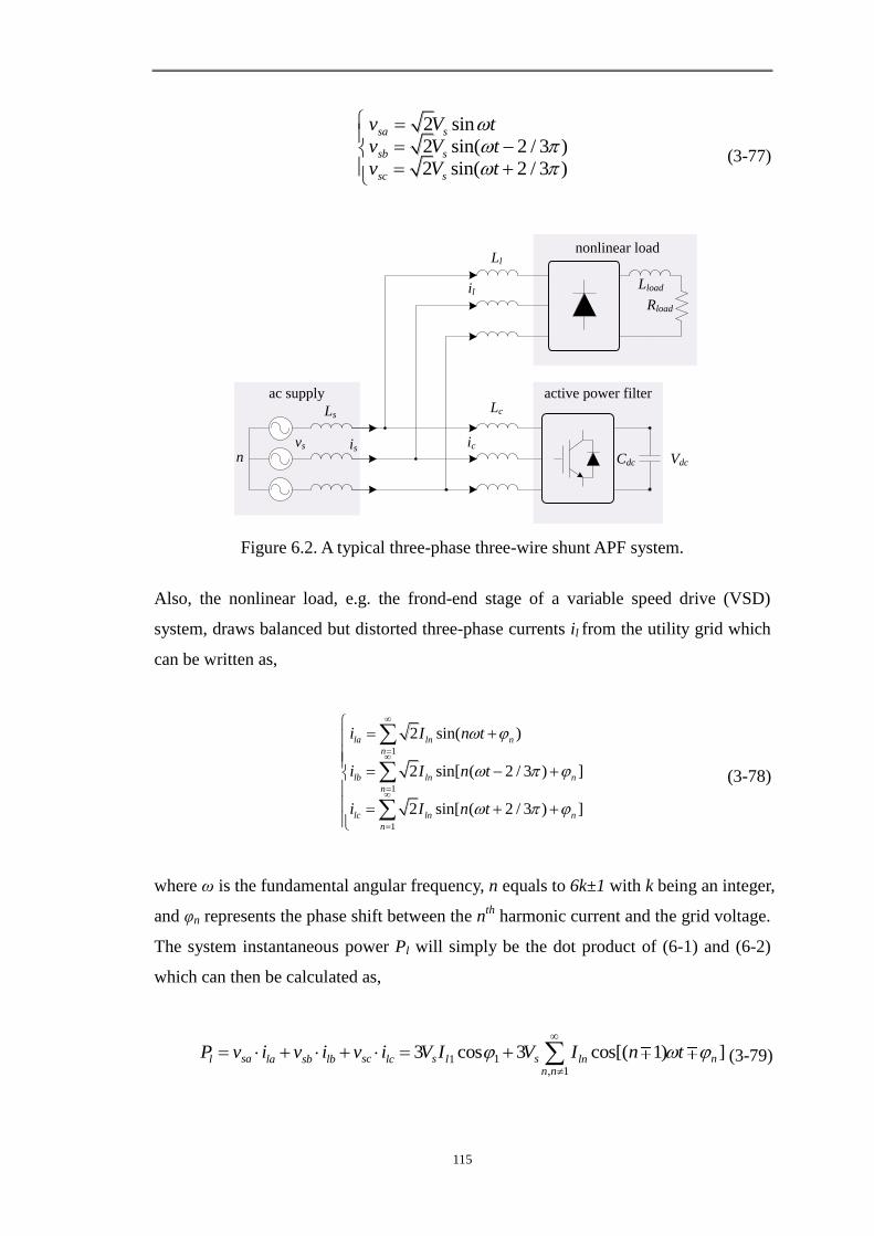
115
2 sin
2 sin( 2 / 3 )
2 sin( 2 / 3 )
sa s
sb s
sc s
v V t
v V t
v V t
(3-77)
nonlinear load
vs is
LsLc
Ll
n
Lload
Rload
il
ic
active power filter
Cdc
ac supply
Vdc
Figure 6.2. A typical three-phase three-wire shunt APF system.
Also, the nonlinear load, e.g. the frond-end stage of a variable speed drive (VSD)
system, draws balanced but distorted three-phase currents il from the utility grid which
can be written as,
1
1
1
2 sin( )
2 sin[ ( 2 / 3 ) ]
2 sin[ ( 2 / 3 ) ]
la ln n
n
lb ln n
n
lc ln n
n
i I n t
i I n t
i I n t
(3-78)
where ω is the fundamental angular frequency, n equals to 6k±1 with k being an integer,
and φn represents the phase shift between the nth
harmonic current and the grid voltage.
The system instantaneous power Pl will simply be the dot product of (6-1) and (6-2)
which can then be calculated as,
11, 1
3 cos 3 cos[( 1) ]sa sc s s nl la sb lb lc l lnn n
P v i v i v i V I V I n t
(3-79)

116
Clearly, the first term on the right hand side of (6-3) represents the active power
demand by the nonlinear loads and the second term will be the harmonic power that
needs to be compensated by the APF. It is interesting to observe that the DC-link
harmonic power is in the order of 6k. This is because, in the stationary reference frame,
the 5th
harmonic current is the negative sequence component while the 7th
is the
positive one, and if rotated into synchronous reference frame, both of them will turn
out to be the 6th
harmonic components [17, 112], which are finally reflected in the
DC-link of APF. Assuming that the DC-link capacitance Cdc is ideally large and the
ripple across the DC bus voltage Vdc is very small, then the harmonic current idcn going
into the DC-link capacitors can be calculated as,
, 1
cos[( 1) ]3 ln n
dcn s
n n dc
I n ti V
V
(3-80)
The resulting ripple voltage vdcn will be,
, 1
cos[( 1) ]3
( 1)
ln n
dcn dcn dcn s
n n dc dc
I n tv i Z V
n C V
(3-81)
It should be noted that the above calculation only applies when the ripple voltage is
kept within an acceptable range so that the interaction between idcn and vdcn can be
neglected. Since the 5th
and 7th
harmonic currents are dominant in the three-phase
three-wire power system, they can subsequently lead to the highest 6th
order ripple
voltage in the DC-link. If it is defined that the voltage variation should be within±a%
(typically a is less than 1) of the nominal bus voltage, the capacitance can then be
simply calculated by only concerning the 6th
harmonic power Sl6 in the DC-link as,
6 6 6
2
100
6 ( ) 6 ( % ) 6
l l ldc
dcn dc dc dc dc
S S SC
V V a V V aV
(3-82)
It is clear from the above equation that for a typical three-phase APF with 400V (±1%)
bus voltage, it is expected to need at least 276μF DC-link capacitance to compensate
1KVA 6th
harmonic power in a 60Hz AC system. In fact, the actual required DC-link

117
capacitance should be even larger than the value calculated from (6-6) because the
ripple currents have significant impact on the lifetime of electrolytic capacitors and
more capacitors should be paralleled to share this burden in a practical system design.
6.3. DC Active Power Filter — DC-link Compensator (DLC)
6.3.1. Principle of DC-link compensator (DLC)
nonlinear load
vs is
LsLc
Ll
n
Lload
Rload
il
ic
active power filter
Cdc
ac supply
Vdc_p
Vdc_n
Vdc iac3 vac3
Vdc_p
Vdc_n
iac3 vac3
dc-link compensator
for 6th harmonic power
four-quadrant
two-quadrant
Lac3
Cac3
Lac3
Cac3
Figure 6.3. The proposed hybrid AC/DC active power filter including a conventional
three-phase three-wire SAPF and a DLC.
Equation (6-3) shows that the harmonic power in a three-phase three-wire system is a
time-varying component with frequency of 6k. Instead of smoothing such harmonics
by using large electrolytic capacitors, the DCL is proposed in this section as shown in
Figure 6.3 to offer an active approach to sink this harmonic power. As shown in Figure
6.3, the conventional shunt APF is equipped with high frequency AC capacitors and
four active switches. In order to provide 6kth
harmonic power, the four switches will be
modulated in such a way that the voltage across the AC capacitor is a sinusoidal
waveform with frequency of 3k. If it is defined that the voltage vac3k and current iac3k of
the AC capacitor are in the following form,
3 32 sin(3 )ac k ac kv V k t (3-83)

118
3
3 3 3 33 2 cos(3 )ac kac k ac k ac k ac k
dvi C k C V k t
dt (3-84)
The instantaneous power provided by this DLC can then be calculated as (the power in
the filter inductor is very small and negligible),
3 3 3 3 3
2
3 3
2 sin(3 ) 3 2 cos(3 )
3 sin(6 )
ac k ac k ac k ac k ac k
ac k ac k
v i V k t k C V k t
k C V k t
(3-85)
The above equation indicates that the DLC is also able to provide 6th
harmonic power
(when k=1) and the amount of harmonic power relates to the AC capacitance with the
following equation,
6
3 2
33
lac
ac
SC
V (3-86)
Comparing (6-10) with (6-6), it is obvious that for compensating the same amount of
6th
harmonic power, the theoretically required capacitance ratio between a
conventional APF and the proposed DLC system will be,
226 6 3
32 2 2
3 3
100 300 25/
6 3 6
dc l l acac
ac dc ac dc
C S S Vm
C aV V aV a
(3-87)
where 3 32 /ac ac dcm V V is the modulation index applied to the DLC converter. For a
very typical system design that has a = 0.5 and mac3 = 0.9, the capacitance can
theoretically be reduced by at least 40.5 times with the help of a DLC, and this is also
the root reason that why film capacitors can be used to replace the expensive
electrolytic ones. Similarly, more DLC converters can be parallel connected into the
DC bus and designed in the above manner to compensate 12th
, 18th
or even higher
order harmonics. However, their contributions are generally very limited because the
voltage ripples caused by them are insignificant. Therefore, the first 6kth
harmonic in
the DC-link will normally be of interest and become the target of the DLC in this
thesis.

119
Some typical operating waveforms of a DLC designed for 6th
harmonic power
compensation are shown in the first three plots of Figure 6.4.
Figure 6.4. Idealized operating waveforms for four-quadrant (b) (c) and two-quadrant (d)
(e) DC-link compensators.
It can be seen that the compensator is in effect a four-quadrant converter that can
produce both positive/negative voltage/current. A potential problem with this
configuration is its increased implementation complexity, because each compensator
requires at least four active switches to operate. Since the DLC is particularly designed
to control harmonic power and energy, which is determined by the square of the
capacitor terminal voltage as expressed by (6-9), and the capacitor voltage is therefore
not necessarily to be negative [113]. A simplified configuration of DLC is then derived
and drawn in top right of Figure 6.3, which is essentially a two-quadrant converter that
can only produce positive capacitor voltage. The typical operating waveforms of the
two-quadrant DLC are then presented in Figure 6.4(d) and (e). It is obvious that this
type of DLC features exactly the same harmonic compensation capacity. Moreover,
this simplification has no impact on the reduction of capacitance, but reduces the cost
and complexity of DLC converter. This is the reason that the two-quadrant DLC will
be eventually selected as the prototype in the experimental verifications.

120
6.3.2. Design of DC-link compensator (DLC)
This sub-section presents the design of a three-phase three-wire shunt APF system
used in comjunction with the proposed DLC to resolve the system harmonic problem.
The overall circuit diagram is shown in Figure 6.3 and the associated system
parameters are listed in Table 6.1. The harmonic power propagated into the DC-link of
APF can be calculated by multiplying the three-phase currents ic of APF converter with
the three-phase AC supply voltages vs. The 6th
harmonic power can then be extracted
by a notch filter (will be elaborated in the following section) tuned at 360Hz and its
magnitude is found to be 200 VA. According to (6-6), in order to keep the voltage
variation within 0.5%, the required capacitance will be,
2 2
6100 / 6 100 200 (6 120 0.5 300 ) 196.49dc l dcC S aV F (3-88)
Compared with the minimum required DC-link capacitance derived in (6-12), the
closest standard capacitance value is 220μF. As discussed above, the capacitance can
be much reduced with the help of the DLC and to compensate the same amount of 6th
harmonic power, the required AC capacitance is only,
2 2
3 6 3/ 3 200 [3 120 (0.9 300 2) ] 4.85ac l acC S V F (3-89)
In this case, a 5μF film capacitor can be used as the AC output capacitor of DLC. Since
most of the harmonics can be cancelled out by this AC capacitor, the main task of the
DC-link capacitor of the APF is to get rid of very high order and switching harmonics.
Therefore, a very small electrolytic capacitor is sufficient, e.g. 30μF, and its main task
is to absorb high frequency harmonics. It is even possible to use film type DC-link
capacitors with the voltage of a 180Hz sinusoidal waveform. Its magnitude is
determined by (6-10) and the phase must be synchronized to the 6th
harmonic power
generated from the AC side in order to achieve perfect cancellation.

121
Table 6.1. System Parameters used for Simulation.
Elements Parameters Values
AC supply
supply voltage Vs 120 V
line frequency f 60 Hz
line impedance Ls 0.2 mH
APF
converter
nominal power Sn 3 kVA
filter inductance Lc 2 mH
DC-link capacitance
Cdc 33 μF
DC-link voltage Vdc 400 V
DC-link
compensator
filter inductance Lac3 0.5 mH
AC capacitance Cac3 5 μF
capacitor voltage Vac3 255 V
switching frequency
fsw 25 kHz
nonlinear
load
(see Fig. 1
for circuit)
smoothing inductance
Ll 2 mH
load inductance Lload 10 mH
load resistance Rload 30 Ω
Gpv Kpv 0.15
τv 0.015
Gcf Kcv 0.1
τc 0.002
6.4. Control of Active Power Filter (APF) and DC-link Compensator
(DLC)
With the review of conventional shunt APFs and comprehensive illustration of the
proposed DLC operating principle, the control implementations for both APF and DLC
will be elaborated in this section as follows.
6.4.1. Control of active power filter (APF)
The APF system is designed to compensate selective harmonic components in the line
current through injecting harmonic currents into the grid with the same amplitude but
opposite phase to the harmonic current produced by nonlinear loads. The control block
diagram of APF system is shown in Figure 6.5, which is composed of an outer DC
voltage controller and an inner current controller with parallel connection of
fundamental and individual harmonic current controllers.
The DC voltage controller is to maintain the DC-link capacitor voltage constant. Its

122
realization can be just the stationary frame proportional-integral (PI) controller Gv(s)
written in (6-14)
Vdc* voltage
control
eq. (6-14)
is
isd*
-
isq* = 0 -
isdfundamental
current
control
eq. (6-15)
fundamental
current
control
eq. (6-15)
resonance
control
eq. (6-16)
resonance
control
eq. (6-16)
vs PLLθs
e-jθs
isq
q - axix current set to 0 for
Unity power factor operation
-
Vdc
++
++
+
+
+
Vmd
Vmqe-jθs
Vm
θs
SPWM
gate
signals
APF
Figure 6.5. Control block diagram of APF.
1
( ) (1 )v pv
v
G s Ks
(3-90)
where Kpv is the proportional gain, and τv is the time constant of the integral term. Gv(s)
should be designed to ensure relative slower dynamic response than the inner current
controllers, so as to avoid transient interference between them.
The output of the DC voltage controller is then fed into the inner current control loop,
acting as the active current reference. For a simple control implementation, only line
currents is were sensed, replacing the complex control system with two set of sensors
to measure both the nonlinear load and APF currents. The reactive current is set as zero
to achieve unity power factor operation. The fundamental current is therefore regulated
using the following PI controller in the synchronous dq frame rotating at the angular
speed of the line voltage vs:
1
( ) (1 )cf cv
c
G s Ks
(3-91)
where Kcv is the proportional gain, and τc is time constant of the integral term.
Proceeding onto the compensation for harmonic currents, it can be alternatively
implemented in either stationary or synchronous frame. It was proved in [114] that a

123
resonant controller in the synchronous frame is more effective, since it represents two
equivalent resonant terms in the stationary frame for compensating a pair of harmonics.
The harmonic current regulation in this APF system is thus implemented in the
synchronous dq frame by using multiple paralleled resonant controllers expressed as,
2 21
( )(6 )
kih
ch
n n
K sG s
s n
(3-92)
where ω, Kih, and k represent the nominal angular frequency, respective resonant gain,
and the highest harmonic order that can be compensated, respectively. The summation
of the outputs of fundamental and harmonic current controllers is subsequently
transformed back into stationary frame and treated as the reference voltage for
modulation of the APF converter.
6.4.2. Control of DC-link compensator (DLC)
As analyzed in previous sections, the DLC proposed in this chapter is to sink the 6th
harmonic power which may cause considerable voltage ripple in the DC-link if its
capacitance cannot meet the required minimum value. The control of the DLC is on the
basis of accurate acquisition of AC capacitor’s voltage reference, with which the
DC-link compensator can cancel out exactly the same account of 6th
harmonic power
flowing into the DC-link of APF.
The gross harmonic power propagated into the DC-link of APF can be first calculated
as,
sa ca sc ccl sb cbS v i v i v i (3-93)
The 6th
harmonic power can then be extracted by a notch filter tuned at 6 times of the
fundamental frequency.
6
2 2
6 6
6( )
l
K sS
s K s (3-94)

124
where K6 determines the Q factor of this second order system and it mainly affects
dynamic response.
The detection of 6th
harmonic power using (6-18) gives rise to the acquisition of AC
capacitor’s voltage reference, and its root mean square (RMS) value can then be
determined by (6-10). It should be noted that, in order to achieve perfect harmonic
cancellation, the starting point of this reference voltage must be locked to the positive
zero-crossing point of 6th
harmonic power, as depicted in Figure 6.4. This can be done
through the phase-locked loop (PLL) and voltage controlled oscillator (VCO)
elements.
The obtained voltage reference is then fed into a classic dual loop controller to regulate
the voltage of the AC capacitor. The outer voltage control loop is realized by a PI
controller in order to minimize the steady-state tracking errors, and a simple
proportional gain is employed in the inner current loop to improve system stability and
dynamic response. It is know that this inner current controller is not necessarily to be
PI, proportional resonant (PR) or other advanced controllers because its steady-state
error will not affect the tracking accuracy of the outer voltage control loop. Besides
this dual loop controller, a feed-forward path of output voltage is also implemented to
decouple the system back electromotive force (EMF) so that the closed-loop
compensators can have smaller contributions to the duty cycle calculation and the
control system can gain more robustness [115]. The final control block diagram for
DLC stage is shown in Figure 6.6.
instantaneous
APF power
calculation
eq. (6-17)
vs
ic
6th harmonic
power
extraction
eq. (6-18)
voltage
reference
calculation
eq. (6-12)
PI-+ -+
iac3
iac3*
vac3
vac3*
P ++
1/Vdc*
PWM
gate
signals
d DLC
dff
d' Sl Sl6
Figure 6.6. Control block diagram of DLC stage.
It should be noted that the DLC can only be activated when the AC capacitor’s voltage
is in the vicinity of zero volt. Otherwise, a large voltage difference Δvac3 between the
voltage reference and the instantaneous voltage of AC capacitor may occur, and very
high dv/dt can result in undesired inrush current in the DLC circuit and thus influence

125
the normal operation of APF. This problem can be prevented by setting a threshold
value ε for Δvac3 to control the activation of DLC and expressed as follows (also as
explicated in Figure 6.7):
*
3 3 3
*
3 3 3
1, )
0, )
ac ac ac
DLC
ac ac ac
v v vA
v v v
(3-95)
where ADLC is the enable signal for DLC, “1” denotes enabling DLC and “0” denotes
disabling DLC.
Δvac3 < ε?
eq. (6-19)
vac3*
vac3
on/offQ
QSET
CLR
S
RNOT
ANDADLC
Figure 6.7. Logic operator for activation of DLC stage.
6.5. Simulation Results
The designed system in Sub-section 6.3.2 is simulated in Matlab/Simulink
environment to prove the concept of the proposed DLC and the simulated results are
shown in Figure 6.8. The relevant parameters used in simulation are listed in Table 6.1.
The APF is running alone with a 33μF DC-link capacitor when t<0.04s. It is obvious that
the capacitance is too small to maintain constant bus voltage and the voltage variation in
the DC-link of APF can be as high as 30V. This voltage variation in turn affects the
current regulation of APF and the total harmonic distortion (THD) in the AC line is
found to be 5.01%. In order to mitigate this undesired voltage ripple, the DLC is
switched on at t = 0.04s and starts to shift the 6th
harmonic power from the DC-link of
APF to itself. As can be seen, the voltage variation of APF is dramatically reduced and
the 6th
voltage ripple across the DC-link is less than 1.2V. The peak-to-peak voltage is
only 5V and it is mainly contributed by other high order harmonics. With this much
smoother DC-link voltage, the current regulation of APF can be more accurate because
of fewer disturbances and the THD of the line current is only 2.06% after operation of

126
the DC-link compensator, which is a very satisfactory result.
Figure 6.8. Simulated results showing the effectiveness of the proposed DLC concept.
6.6. Prototype Setup and Experiment Verifications
6.6.1. Description of proposed hybrid AC/DC power filter prototype
The proposed hybrid AC/DC active filters system was then validated via proportional
scaled-down laboratory tests. The experimental circuit consists of a 2kVA APF, a DLC
and a three-phase nonlinear load configured as shown in Figure 6.2. The control
algorithms presented in Section 6.4 for both APF and DLC were executed on a
dSPACE1103 real-time platform, and the digital signal processor TMS 240F240 was
employed with its sampling frequency being set as 12.5kHz in the controller board,

127
which is the same as the switching frequency. The schematic diagram of overall
experimental setup is shown in Figure 6.9. A transfer switch is used in the nonlinear
load, allowing the APF system to be subjected to a 100% to 66.7% step-down
nonlinear load change. All parameters in the experiment are listed in Table 6.2.
Figure 6.9. Experimental setup of the APF system with a DLC.
Table 6.2. System parameters used for scale-down laboratory experiments.
Elements Parameters Values
AC supply
supply voltage Vs 87 V
line frequency f 60 Hz
line impedance Ls 0.2 mH
APF
converter
nominal power Sn 3 kVA
filter inductance Lc 2 mH
DC-link capacitance
Cdc 33 μF
dc-link voltage Vdc 300 V
DC-link
compensator
filter inductance Lac3 0.5 mH
AC capacitance Cac3 5 μF
capacitor voltage Vac3 265 V
switching frequency
fsw 12.5 kHz
nonlinear
load
(see Fig. 1
for circuit)
smoothing inductance
Ll 2 mH
load inductance Lload 10 mH
load resistance Rload 30 Ω
Gpv Kpv 0.2
τv 0.02
Gcf Kcv 0.1
τc 0.001

128
6.6.2. Experiment Results
The first set of experimental results is shown in Figure 6.10, during which the APF
system is running alone and supplying 100% nonlinear load in the steady state. In this
case, the designed DC-link capacitance (220μF) of the APF system in Sub-section
6.3.2 was intentionally replaced by two 15μF MKP1848 film type DC-link capacitors
from Vishay in order to examine the ripple of DC-link voltage. As anticipated, it is
obvious that the capacitance is too small to maintain constant bus voltage and the
voltage variation in the DC-link of APF can be as high as approximately 20V.
Figure 6.10. Experimental results of steady state performance of APF system with a
33μF dc-link capacitance.
The harmonic content of the DC-link voltage is listed in Table 6.3 and it is clear that
the 6th
harmonic voltage is dominant with amplitude of 7.76V. Such voltage variation
may in turn affect the current regulation of the APF and total harmonic distortion
(THD) in the AC line current is found to be 4.77% with 0.16A 5th
harmonic current and
0.13A 7th
harmonic current, and its detailed spectrum is shown in Figure 6.11.
Table 6.3. Harmonic content in the DC-link voltage.
Unit (Volt) 6th
12th
18th
w/o DLC 7.76 1.12 0.29
w DLC 0.36 0.84 0.23
The DLC was subsequently loaded to mitigate the undesired voltage ripple in the
DC-link. Figure 6.12 then shows the steady-state performance of both APF and DLC

129
stages.
Figure 6.11. Harmonic current spectrum: APF versus APF with a DLC.
(a)
(b)
Figure 6.12. Experimental results of steady state performance of: (a) APF system; (b)
dc-link compensator.

130
As can be seen in Figure 6.12(a), the voltage variation of APF is dramatically reduced
since the DLC can shift the 6th
harmonic power from the DC-link of APF to itself. The
peak-to-peak value of the reduced DC-link voltage is around 6V, which is mainly
contributed by other higher order harmonics. With the help of the DLC, the 6th
harmonic voltage is suppressed from 7.76V to 0.36V and even the 12th
and 18th
harmonic voltages are also slightly decreased (see Table 6.3). The corresponding effect
is of course better current regulation. With this much smoother DC-link voltage, the
current regulation of the APF can be more accurate because of less disturbances and
the THD of line current is now 4.18% after the operation of DLC. The 5th
and 7th
harmonics in the line current are reduced to 0.11A and 0.08A, respectively. On the
DLC end, the peak value of stored 6th
harmonic power Sl6 is read approximately as
200VA and this signal is generated from a digital-analog converter (DAC) channel. To
sink the exact amount of 6th
harmonic power based on (6-10), the voltage of the AC
capacitor is controlled as the half sinusoidal waveform with its peak value of 265V, as
shown in Figure 6.12(b). These two waveforms are in accordance with those shown in
Figure 6.4(a) and (d), and they prove the theoretical studies presented before.
The proposed APF system with DLC enabled is finally subjected to a 100% to 50%
step down load change and the experimental results are shown in Figure 6.13. The
sudden load decrease causes the DC-link voltage Vdc to increase to 360V. This
overshoot voltage is slightly higher than expected which is partly due to the small
DC-link capacitance used, and also partly due to the non-optimized voltage loop
controller design. The DC-link voltage can finally be kept at the nominal value 300V
within 5 line cycles and its variation also gets smaller after this transient state. As seen
from Figure 6.13(a), the transient voltage spurt may directly affect the current
regulation, and the grid current is found to have slight distortion lasting for about half a
cycle time. However, this distortion is not obvious and has no impact on the APF
system performance. Figure 6.13(b) then demonstrates that the actual voltage of AC
capacitor of the DLC can smoothly change from 265V to 183V, which is in accordance
to the change of harmonic power produced by the nonlinear load. In this case, the 6th
harmonic power can always be absorbed by the DLC and the variation of DC-link
voltage can be maintained within an acceptable range at any load conditions.

131
(a)
(b)
Figure 6.13. Experimental results of proposed APF system with a DLC when subjected
to a 100% to 50% step-down load change.
6.7. Conclusions
This chapter presented a hybrid AC/DC active power filter which is the combination of
a conventional APF in three-phase three-wire power systems and a proposed DLC. The
attractiveness of the presented system is the significant capacitance reduction which
can be achieved in the APF without compromising its performance and adding
implementation complexity. The demonstrated results show that good harmonic
compensation can be accomplished with only a 30μF DC-link capacitor and a 5μF AC
capacitor used in the hybrid active filters system. Moreover, with the help of film

132
capacitors, the reliability of APF can be enhanced, and its lifetime can be expanded
and the system weight and costs can all be reduced in the long term running, making it
a very promising system solution for power quality issues.
133
Chapter 7 Conclusions and Recommendations
7.1. Conclusions
A hybrid AC/DC microgrid features higher operation efficiency, better integration
compatibility, more power capacity and control flexibilities to fulfill the overall system
reliability and power quality requirements which can hardly be achieved by any
individual microgrid or single DG system. The core point of the research work in this
thesis is to develop proper control strategies for reliable and efficient operations of
hybrid microgrids whose potential benefits have not been exploited in previous
literature researches.
In Chapter 2, the concept of hybrid AC/DC microgrid is introduced after an
introductory review of DG and microgrid system. The feasibility of existing AC or DC
architecture including their relevant advantages and various applications is
summarized. An example of hybrid microgrid is then given to show its basic
components as well as typical overall structure. The main advantages of the proposed
hybrid AC/DC microgrids are subsequently summarized as: 1) higher conversion
efficiency because of the elimination of unnecessary multi-conversion processes; 2)
simplification of equipment and cost reduction of electronic products because of the
elimination of front-end rectifiers for DC or ACwC loads in the current AC grid; 3)
harmonic attenuation in AC system with the contribution of the interfacing converter
which can sink the harmonic current in AC side into DC microgrid.
After an introduction of the proposed hybrid architecture, a hierarchical control
scheme is proposed in Chapter 3 for managing reliable and economical operations of a
stand-alone DC microgrid. The proposed control scheme includes: 1) Hierarchical
Level I (HLI) is the primary control to maintain the bus voltage within specified limits
through changing the operation modes of converters. The bus voltage in this level
essentially acts as an indicator of supply-demand balance. A wireless control is
therefore implemented for reliable operation of the grid; 2) Hierarchical Level II (HLII)
is the secondary control to achieve real-time voltage regulation capability for the

134
system power modules and prioritizations for charge/discharge of the batteries with
different SoCs. A reasonable compromise between the maximum power harvesting and
effective battery charging is addressed in this level using coordination control based on
a central energy management system; 3) Hierarchical Level III (HLIII) handles
extreme operation conditions such as sudden load and source change due to system
failures through load shedding or ballast.
Upon reliable operation of DC microgrids, the research focus is then moved onto the
development of proper control schemes for reliable operation of autonomous hybrid
AC/DC microgrids. With this intention, a GPS control is proposed in Chapter 4, where
power balance maintenance within each sub-grid and power exchange management
between two sub-grids are both taken into account. The power balance within each
sub-grid is maintained by means of source droop control for power sharing among DG
units in AC or DC sub-grid, while a rule of power exchange between two sub-grids is
established and realized by the proposed GPS control. With GPS realization, all
sources dispersed in both sub-grids are capable of sharing the total loads throughout
the entire hybrid system. By doing so, the obvious advantages can be summarized as: 1)
any single point of failure due to overstress in a certain source can be avoided; 2)
sources with slower response to load transients are expected to have smaller variations,
thus resulting in a short transient period; 3) design of the capacity of each sub-grid will
no longer be constrained by respective local load profiles. Rather, their capacities can be
chosen according to the entire load profiles since DGs in one network can be viewed as
the back-up reserve for the other one; 4) all elements are managed in decentralized
manner without information exchange. This provides an emergency operation scheme
during communication failures for complex system with mass communications.
Concerning variable random loads and intermittent renewable sources, the hybrid
microgrid can hardly be fully autonomous without DSs for energy buffering, power
balancing and fault riding-through. With the consideration of integrating DSs into
hybrid AC/DC system, a three-bus AC/DC/DS hybrid infrastructure is proposed in
Chapter 5. In this layout, DGs and DSs with the same type are placed in the relevant
AC, DC or DS bus in order to avoid the complexity of power management and enforce
coincident control scheme to DGs and DSs. For managing the power flow and
maintaining reliable operations of such a complex system, Chapter 5 proposes a

135
distributed control, which includes: 1) a fully decentralized control, in terms of source
droop control for LPS in individual AC or DC network, GPS throughout AC and DC
network and demand droop control for SPS among DS units, has been developed for
decentralized operations; 2) a multi-level power exchange control for managing
activation sequences among LPS, GPS and SPS has been proposed to restrain
unnecessary power exchange due to GPS and reduce DS operations in SPS. With the
proposed distributed control, each power module in the hybrid system can operate
independently because of the fully decentralized control. The reliability of the overall
hybrid system is therefore enhanced. Moreover, the optimal degree can also be
improved because of the power exchange control since unnecessary power exchange
and storage usage are reduced.
After the investigation on the basic operation of the hybrid system, further
consideration of power quality issue and alternative solutions in hybrid microgrids are
addressed in Chapter 6. In that chapter, the functionality of the interlinking converter
(IC) is broadened to serve as a shunt APF, attenuating the harmonic current due to the
nonlinear load in AC sub-grid. By doing so, the harmonic current will be injected into
DC side, result in voltage ripples in the bus voltage due to the ripple power injection.
To reduce voltage ripple in DC bus, a DC-link compensator (DLC) is proposed in
Chapter 6 for decoupling the harmonic power from the DC-link of the APF. With proper
system sizing and design, most of the harmonic power can be cancelled out by the
DC-link compensator and the electrolytic capacitors used in the shunt APF system will
be only responsible for filtering very high order or system switching harmonics, and the
overall system size can therefore be significantly reduced. The electrolytic capacitors
used in the shunt APF system can eventually be replaced by small film capacitors and
the final system may feature much reduced size and costs, extremely long lifetime and
very compact system design.
In a summary, the distributed control strategy and power quality improvement for
hybrid AC-DC microgrid have been verified in theory, simulation and experiment, and
will definitely facilitate the application and development of hybrid AC-DC microgrid in
low voltage distribution systems.
136
7.2. Recommendations
Systematic research on proper control scheme for reliable operations and power
quality improvement of hybrid AC/DC microgrids are carried out in this thesis. Several
topics which are worthwhile for further in-depth investigation have not been
investigated in this work. Interesting research topics recommended for future study are
given as below.
Sources in hybrid AC/DC system are ideal DC sources, which might be impractical in
practical applications. It is recommended that the development of proper control
schemes should be combined with the development of models of real micro-sources,
such as micro-turbine and renewable sources. Characteristics and dynamic response of
specific micro-sources should be incorporated with the development of new control
schemes. Moreover, distributed storage with different features like high power and
high energy can be coordinately managed. The hybridization usage of distributed
storages is recommended.
To improve the load sharing accuracy and system transient stability, it is possible to
implement the other existing droop methods, such as droop control with virtual output
impedance, power derivative and integral terms, and harmonic current sharing, to this
hybrid microgrid system. Moreover, most of the research works related to droop control
are concentrated on its application with voltage source inverter (VSI). The droop
method applied to current source inverter (CSI) is seldom investigated. For the CSI, the
L filter at AC side can be saved, and therefore, the output impedance of inverter can be
reduced. However, the problem with CSI is the input L filter must be large. Therefore, it
might be interesting to investigate proper control strategy for the purpose of reducing L
filter while maintaining good performance.
The global stability of DC microgrids with a specific control strategy is affected by the
stability of individual source/storage/load converter and their interactions. Stability
issues for individual converter have been widely studied in the literatures with primary
frequency domain analysis. However, the use of frequency domain analysis is around a
single operation point and does not consider the overall interactions and boundary limits

137
of DC systems. Furthermore, the stability issues due to the mode switching are seldom
found in the literature. Developing a theory of stability evolution for multi-converter
based DC microgrids becomes challenge especially when the state transitions are taken
into account.
In global power sharing control, the stability of AC or DC microgrids depends on the
overall stability of the droop controlled parallel DGs, which have been widely
investigated in the literatures. Combining both sub-grids with the IC together, the IC can
be viewed as the load disturbance for each sub-grid. The global stability issue therefore
includes the stability of individual sub-grid and the interactions between both sub-grids
through the IC. The global stability analysis throughout hybrid AC/DC microgrids is
not as straightforward as the stability analysis for single DG or sub-grid and it is
therefore recommended as an interesting research topic for future study.
Finally, only nonlinear loads in AC microgrid are considered in this research work. The
load disturbances including both unbalanced and nonlinear loads can be also taken into
account in the hybrid microgrid system in the future.

138
Author’s Publications
Journal Publications
1. C. Jin, P. Wang, J. Xiao, Y. Tang, and F. H. Choo, "Implementation of
hierarchical control in dc microgrids," IEEE Trans. Ind. Electron., vol. PP, no. 99,
pp. 1-1. 2013
2. P. Wang, C. Jin, D. Zhu, P. C. Loh, and F. H. Choo, "Distributed Control for
Autonomous Operation of a Three-Port ac/dc/ds Hybrid Microgrid," Industrial
Electronics, IEEE Transactions on , vol.PP, no.99, pp.1,1. (early access)
3. Y. Tang, D. Zhu, C. Jin, P. Wang, and F. Blaabjerg, "A Three-Level
Quasi-Two-Stage Single-Phase PFC Converter with Flexible Output Voltage and
Improved Conversion Efficiency," Power Electronics, IEEE Transactions on ,
vol.PP, no.99, pp.1,1. (early access)
4. Y. Tang, F. Blaabjerg, P. C. Loh, C. Jin, and P. Wang, "Decoupling of Fluctuating
Power in Single-Phase Systems through a Symmetrical Half-Bridge
Circuit," Power Electronics, IEEE Transactions on , vol.PP, no.99, pp.1,1. (early
access)
Conference Publications
1. C. Jin, and P. Wang, "Enhancement of low voltage ride-through capability for
wind turbine driven dfig with active crowbar and battery energy storage system,"
in Proc. Power and Energy Society General Meeting, 2010 IEEE, 2010, pp. 1-8.
2. C. Jin, P. C. Loh, P. Wang, Y. Mi, and F. Blaabjerg, "Autonomous operation of
hybrid ac-dc microgrids," in Proc. Sustainable Energy Technologies (ICSET),
2010 IEEE International Conference on, 2010, pp. 1-7.
3. P. Wang, X. Liu, C. Jin, P. C. Loh, and F. H. Choo, "A hybrid ac/dc micro-grid
architecture, operation and control," in Proc. Power and Energy Society General
Meeting, 2011 IEEE, 2011, pp. 1-8.

139
4. W. Mo, P. C. Loh, C. Jin, P. Wang, and F. Blaabjerg, "Six transformer based
asymmetrical embedded z-source inverters," in Proc. Applied Power Electronics
Conference and Exposition (APEC), 2013 Twenty-Eighth Annual IEEE, 2013, pp.
2273-2279.
5. C. Jin, Y. Tang, P. Wang, and X. Liu, "Reduction of Dc-link Capacitance for
Three-Phase Three-Wire Shunt Active Power Filters," in IECON 2013 - 39th
Annual Conference on IEEE Industrial Electronics Society , vol., no., pp., 10-13
Nov. 2013.
6. D. Zhu, Y. Tang, C. Jin, and P. Wang, "A High Efficiency Single-Phase PFC
Converter for Electric Vehicle Charger Applications," in IECON 2013 - 39th
Annual Conference on IEEE Industrial Electronics Society , vol., no., pp., 10-13
Nov. 2013.

140
Bibliography
[1] R. C. Dugan and T. E. McDermott, "Distributed generation," IEEE Industry
Applications Magazine, vol. 8, no. 2, pp. 19-25, 2002
[2] F. Blaabjerg, R. Teodorescu, M. Liserre and A. V. Timbus, "Overview of control
and grid synchronization for distributed power generation systems," IEEE Trans.
Ind. Electron., vol. 53, no. 5, pp. 1398-1409, 2006
[3] R. H. Lasseter, "Microgrids,"in Proc. IEEE Power Engineering Society
Transmission and Distribution Conference, 2002, pp. 305-308
[4] J. M. Carrasco, L. G. Franquelo, J. T. Bialasiewicz, E. Galvan, R. C. P. Guisado,
M. A. M. Prats, J. I. Leon and N. Moreno-Alfonso, "Power-electronic systems
for the grid integration of renewable energy sources: A survey," IEEE Trans. Ind.
Electron., vol. 53, no. 4, pp. 1002-1016, 2006
[5] D. Boroyevich, I. Cvetkovic, D. Dong, R. Burgos, W. Fei and F. Lee, "Future
electronic power distribution systems a contemplative view,"in Proc.
Optimization of Electrical and Electronic Equipment (OPTIM), 2010 12th
International Conference on, 2010, pp. 1369-1380
[6] Y. Sozer and D. A. Torrey, "Modeling and control of utility interactive inverters,"
IEEE Trans. Power Electron., vol. 24, no. 11, pp. 2475-2483, 2009
[7] F. Blaabjerg, Z. Chen and S. B. Kjaer, "Power electronics as efficient interface in
dispersed power generation systems," IEEE Trans. Power Electron., vol. 19, no.
5, pp. 1184-1194, 2004
[8] J. A. Peas Lopes, C. L. Moreira and A. G. Madureira, "Defining control strategies
for microgrids islanded operation," Power Systems, IEEE Transactions on, vol.
21, no. 2, pp. 916-924, 2006
[9] Y. Ito, Y. Zhongqing and H. Akagi, "Dc microgrid based distribution power
generation system,"in Proc. Power Electronics and Motion Control Conference,
2004. IPEMC 2004. The 4th International, 2004, pp. 1740-1745 Vol.1743
[10] P. Biczel, "Power electronic converters in dc microgrid,"in Proc. Compatibility
in Power Electronics, 2007. CPE '07, 2007, pp. 1-6
[11] X. Lie and C. Dong, "Control and operation of a dc microgrid with variable
generation and energy storage," IEEE Trans. Power Del., vol. 26, no. 4, pp.
2513-2522, 2011
[12] X. Liu, P. Wang and P. C. Loh, "A hybrid ac/dc microgrid and its coordination
control," IEEE Trans. Smart Grid, vol. 2, no. 2, pp. 278-286, Jun. 2011
[13] D. Salomonsson, L. Soder and A. Sannino, "An adaptive control system for a dc
microgrid for data centers," IEEE Trans. Ind. Appl., vol. 44, no. 6, pp. 1910-1917,
Nov. 2008
[14] P. Wang, L. Goel, X. Liu and F. H. Choo, "Harmonizing ac and dc: A hybrid
ac/dc future grid solution," Power and Energy Magazine, IEEE, vol. 11, no. 3, pp.
76-83, May 2013
[15] J. M. Guerrero, L. Huang and J. Uceda, "Control of distributed uninterruptible
power supply systems," IEEE Trans. Ind. Electron., vol. 55, no. 8, pp. 2845-2859.
Aug. , 2008
[16] J. Schonberger, R. Duke and S. D. Round, "Dc-bus signaling: A distributed
control strategy for a hybrid renewable nanogrid," IEEE Trans. Ind. Electron.,
vol. 53, no. 5, pp. 1453-1460, Oct. 2006
[17] C. Lascu, L. Asiminoaei, I. Boldea and F. Blaabjerg, "High performance current
141
controller for selective harmonic compensation in active power filters," IEEE
Trans. Power Electron., vol. 22, no. 5, pp. 1826-1835, 2007
[18] T. McNichol: ‘Ac/dc: The savage tale of the first standards war’ (John Wiley
and Sons, 2006)
[19] M. E. Baran and N. R. Mahajan, "Dc distribution for industrial systems:
Opportunities and challenges," IEEE Trans. Ind. Appl., vol. 39, no. 6, pp.
1596-1601, Nov. 2003
[20] R. S. Balog, W. W. Weaver and P. T. Krein, "The load as an energy asset in a
distributed dc smartgrid architecture," IEEE Trans. Smart Grid, vol. 3, no. 1, pp.
253-260, Mar. 2012
[21] A. Sannino, G. Postiglione and M. H. J. Bollen, "Feasibility of a dc network for
commercial facilities," IEEE Trans. Ind. Appl., vol. 39, no. 5, pp. 1499-1507, Sep.
2003
[22] P.-W. Lee , Y.-Z. Lee and B.-T. Lin, "Power distribution systems for future
homes,"in Proc. IEEE Int. Conf. Power Electronics and Drive Systems, (PEDS
'99)1999, pp. 1140-1146
[23] H. Kakigano, Y. Miura and T. Ise, "Configuration and control of a dc microgrid
for residential houses,"in Proc. Transm. Distrib. Conf.Expo.: Asia Pacific, 2009,
pp. 1-4
[24] K. Engelen, E. Leung Shun, P. Vermeyen, I. Pardon, R. D'Hulst, J. Driesen and
R. Belmans, "The feasibility of small-scale residential dc distribution systems,"in
Proc. IEEE Annu. Conf. Ind. Electron, (IECON), 2006, pp. 2618-2623
[25] H. Valderrama-Blavi, J. M. Bosque, F. Guinjoan, L. Marroyo and L.
Martinez-Salamero, "Power adaptor device for domestic dc microgrids based on
commercial mppt inverters," IEEE Trans. Ind. Electron., vol. 60, no. 3, pp.
1191-1203, Mar. , 2013
[26] D. J. Hammerstrom, "Ac versus dc distribution systemsdid we get it right?,"in
Proc. IEEE Power Eng. Soc. Gen. Meet., 2007, pp. 1-5
[27] P. Tulpule, S. Yurkovich, J. Wang and G. Rizzoni, "Hybrid large scale system
model for a dc microgrid,"in Proc. American Control Conf. (ACC), 2011, pp.
3899-3904
[28] T. M. Gruzs and J. Hall, "Ac, dc or hybrid power solutions for today's
telecommunications facilities,"in Proc. IEEE Int.Telecommun. Energy Conf.
(INTELEC), 2000, pp. 361-368
[29] D. Salomonsson and A. Sannino, "Low-voltage dc distribution system for
commercial power systems with sensitive electronic loads," IEEE Trans. Power
Del., vol. 22, no. 3, pp. 1620-1627, Jul. 2007
[30] H. Kakigano, M. Nomura and T. Ise, "Loss evaluation of dc distribution for
residential houses compared with ac system,"in Proc. 2010 Int. Power Electron.
Conf. (IPEC), Jun. 21-24, 2010, pp. 480-486
[31] A. Pratt, P. Kumar and T. V. Aldridge, "Evaluation of 400v dc distribution in
telco and data centers to improve energy efficiency,"in Proc. IEEE Int.
Telecommun. Energy Conf. (INTELEC), Sept. 30 - Oct. 4, 2007, pp. 32-39
[32] M. Amin, Y. Arafat, S. Lundberg and S. Mangold, "Low voltage dc distribution
system compared with 230 v ac,"in Proc. IEEE Electrical Power and Energy
Conf. (EPEC), Oct. 3-5, 2011, pp. 340-345
[33] H. Kakigano, Y. Miura and T. Ise, "Low-voltage bipolar-type dc microgrid for
super high quality distribution," IEEE Trans. Power Electron., vol. 25, no. 12, pp.
3066-3075, Dec. 2010
[34] A. Kwasinski and C. N. Onwuchekwa, "Effects of instantaneous constant-power

142
loads on dc micro-grids for sustainable power systems,"in Proc. 2010 Int. Power
Electron. Conf. (IPEC), Jun. 21-24, 2010, pp. 862-869
[35] A. Kwasinski and C. N. Onwuchekwa, "Dynamic behavior and stabilization of
dc microgrids with instantaneous constant-power loads," IEEE Trans. Power
Electron., vol. 26, no. 3, pp. 822-834, Mar. 2011
[36] X. Feng, J. Liu and F. C. Lee, "Impedance specifications for stable dc distributed
power systems," IEEE Trans. Power Electron., vol. 17, no. 2, pp. 157-162, Mar.
2002
[37] J. Guerrero, P. C. Loh, T.-L. Lee and M. Chandorkar, "Advanced control
architectures for intelligent microgrids—part ii: Power quality, energy storage,
and ac/dc microgrids," IEEE Trans. Ind. Electron., vol. 60, no. 4, pp. 1263-1270,
Apr. , 2013
[38] T. Ackermann, G. Andersson and L. Söder, "Distributed generation: A
definition," Electric Power Systems Research, vol. 57, no. 3, pp. 195-204, 2001
[39] W. El-Khattam and M. M. A. Salama, "Distributed generation technologies,
definitions and benefits," Electric Power Systems Research, vol. 71, no. 2, pp.
119-128, 2004
[40] G. Pepermans, J. Driesen, D. Haeseldonckx, R. Belmans and W. D'Haeseleer,
"Distributed generation: Definition, benefits and issues," Energy Policy, vol. 33,
no. 6, pp. 787-798, 2005
[41] C. Smallwood, "Distributed generation in autonomous and nonautonomous
micro grids,"in Proc. IEEE Rural Electric Power Conference, 2002, pp.
D1-D1_6
[42] P. P. Barker and R. W. De Mello, "Determining the impact of distributed
generation on power systems: Part 1 - radial distribution systems,"in Proc.
Seattle, WA, 2000, pp. 1645-1656
[43] M. T. Doyle, "Reviewing the impacts of distributed generation on distribution
system protection,"in Proc. Chicago, IL, 2002, pp. 103-105
[44] Y. Zoka, H. Sasaki, N. Yorino, K. Kawahara and C. C. Liu, "An interaction
problem of distributed generators installed in a microgrid,"in Proc. IEEE
International Conference on Electric Utility Deregulation, Restructuring and
Power Technologies (DRPT2004), 2004, pp. 795-799
[45] N. Hatziargyriou, "Microgrids," IEEE Power and Energy Magazine, vol. 6, no.
3, pp. 26-30, 2008
[46] A. Arulampalam, M. Barnes, A. Engler, A. Goodwin and N. Jenkins, "Control of
power electronic interfaces in distributed generation microgrids," International
Journal of Electronics, vol. 91, no. 9, pp. 503-523, 2004
[47] R. H. Lasseter: ‘Integration of distributed energy resources — the certs
microgrid concept’. Available: http://certs.lbl.gov/certs-pubs.html, 2002
[48] R. H. Lasseter and M. Erickson: ‘Integration of battery-based energy storage
element in the certs microgrid’. Available: http://certs.lbl.gov/certs-pubs.html,
2009
[49] J. D. Kueck: ‘Microgrid energy management system’. Available:
http://certs.lbl.gov/certs-pubs.html, 2003
[50] H. Jiayi, J. Chuanwen and X. Rong, "A review on distributed energy resources
and microgrid," Renewable and Sustainable Energy Reviews, vol. 12, no. 9, pp.
2465-2476, 2008
[51] R. H. Lasseter and P. Paigi, "Microgrid: A conceptual solution,"in Proc. Power
Electronics Specialists Conference, 2004. PESC 04. 2004 IEEE 35th Annual,
2004, pp. 4285-4290 Vol.4286

143
[52] P. Piagi and R. H. Lasseter, "Autonomous control of microgrids,"in Proc. Power
Engineering Society General Meeting, 2006. IEEE, 2006, pp. 8 pp.
[53] S. Xu, S. Lukic and A. Q. Huang, "Dc zonal micro-grid architecture and
control,"in Proc. IECON 2010 - 36th Annual Conference on IEEE Industrial
Electronics Society, 2010, pp. 2988-2993
[54] J. M. Guerrero, J. C. Vasquez, J. Matas, L. G. de Vicuna and M. Castilla,
"Hierarchical control of droop-controlled ac and dc microgrids—a general
approach toward standardization," IEEE Trans. Ind. Electron., vol. 58, no. 1, pp.
158-172, Jan. 2011
[55] X. Cao , J. Chen , Y. Xiao and Y. Sun, "Building-environment control with
wireless sensor and actuator networks: Centralized versus distributed," IEEE
Trans. Ind. Electron., vol. 57, no. 11, pp. 3596-3605, Nov. , 2010
[56] S. K. Mazumder, M. Tahir and K. Acharya, "Master-slave current-sharing
control of a parallel dc-dc converter system over an rf communication interface,"
IEEE Trans. Ind. Electron., vol. 55, no. 1, pp. 59-66, Jan. , 2008
[57] J. M. Guerrero, J. Matas, V. Luis Garcia de, M. Castilla and J. Miret,
"Decentralized control for parallel operation of distributed generation inverters
using resistive output impedance," IEEE Trans. Ind. Electron., vol. 54, no. 2, pp.
994-1004, Apr. , 2007
[58] J. M. Guerrero, M. Chandorkar, T. Lee and P. C. Loh, "Advanced control
architectures for intelligent microgrids—part i: Decentralized and hierarchical
control," IEEE Trans. Ind. Electron., vol. 60, no. 4, pp. 1254-1262, Apr. , 2013
[59] L. Hao, C. Bong Jun, Z. Weihua and S. Xuemin, "Stability enhancement of
decentralized inverter control through wireless communications in microgrids,"
IEEE Trans. Smart Grid, vol. 4, no. 1, pp. 321-331, Mar. , 2013
[60] T.-F. Wu, Y.-E. Wu, H.-M. Hsieh and Y.-K. Chen, "Current weighting
distribution control strategy for multi-inverter systems to achieve current
sharing," IEEE Trans. Power Electron., vol. 22, no. 1, pp. 160-168, Jan. , 2007
[61] K. Sun, Z. Li, X. Yan and J. M. Guerrero, "A distributed control strategy based
on dc bus signaling for modular photovoltaic generation systems with battery
energy storage," IEEE Trans. Power Electron., vol. 26, no. 10, pp. 3032-3045,
Oct. 2011
[62] S. Anand, B. G. Fernandes and M. Guerrero, "Distributed control to ensure
proportional load sharing and improve voltage regulation in low-voltage dc
microgrids," IEEE Trans. Power Electron., vol. 28, no. 4, pp. 1900-1913, Apr. ,
2013
[63] J. Bryan, R. Duke and S. Round, "Decentralized generator scheduling in a
nanogrid using dc bus signaling,"in Proc. IEEE Power Eng. Soc. General
Meeting, 2004, pp. 977-982
[64] J.-S. Moon, J.-H. Lee, I.-Y. Ha, T.-K. Lee and C.-Y. Won, "An efficient battery
charging algorithm based on state-of-charge estimation for electric vehicle,"in
Proc. Int. Electrical Machines and Systems Conf. (ICEMS), Aug. 20-23, 2011, pp.
1-6
[65] P. Waltari, T. Suntio, A. Tenno and R. Tenno, "The effects of intermittent
charging on vrla battery life expectancy in telecom applications,"in Proc. IEEE
Int.Telecommun. Energy Conf. (INTELEC), 2002, pp. 121-127
[66] M. Bhatt, W. G. Hurley and W. H. Wolfle, "A new approach to intermittent
charging of valve-regulated lead-acid batteries in standby applications," IEEE
Trans. Ind. Electron., vol. 52, no. 5, pp. 1337-1342, Oct. 2005
[67] S. Armstrong, M. E. Glavin and W. G. Hurley, "Comparison of battery charging

144
algorithms for stand alone photovoltaic systems,"in Proc. IEEE Power Electron.
Specialists Conf. (PESC), Jun. 15-19 2008, pp. 1469-1475
[68] X. Liu, P. Wang, P. C. Loh, F. Gao and F. H. Choo, "Control of hybrid
battery/ultra-capacitor energy storage for stand-alone photovoltaic system,"in
Proc. Energy Conversion Congress and Exposition (ECCE), 2010 IEEE, 2010,
pp. 336-341
[69] O. Tremblay, L. A. Dessaint and A. I. Dekkiche, "A generic battery model for
the dynamic simulation of hybrid electric vehicles,"in Proc. Vehicle Power and
Propulsion Conference, 2007. VPPC 2007. IEEE, 2007, pp. 284-289
[70] T. Esram and P. L. Chapman, "Comparison of photovoltaic array maximum
power point tracking techniques," Energy Conversion, IEEE Transactions on, vol.
22, no. 2, pp. 439-449, 2007
[71] S. Jain and V. Agarwal, "A new algorithm for rapid tracking of approximate
maximum power point in photovoltaic systems," Power Electronics Letters,
IEEE, vol. 2, no. 1, pp. 16-19, 2004
[72] N. Femia, G. Petrone, G. Spagnuolo and M. Vitelli, "Optimization of perturb
and observe maximum power point tracking method," IEEE Trans. Power
Electron., vol. 20, no. 4, pp. 963-973, 2005
[73] F. Liu , S. Duan , F. Liu , B. Liu and Y. Kang, "A variable step size inc mppt
method for pv systems," IEEE Trans. Ind. Electron., vol. 55, no. 7, pp.
2622-2628, 2008
[74] M. C. Chandorkar, D. M. Divan and R. Adapa, "Control of parallel connected
inverters in standalone ac supply systems," IEEE Trans. Ind. Appl., vol. 29, no. 1,
pp. 136-143, 1993
[75] A. Tuladhar, K. Jin, T. Unger and K. Mauch, "Parallel operation of single phase
inverter modules with no control interconnections,"in Proc. Applied Power
Electronics Conference and Exposition, 1997. APEC '97 Conference Proceedings
1997., Twelfth Annual, 1997, pp. 94-100 vol.101
[76] C.-C. Hua, K.-A. Liao and J.-R. Lin, "Parallel operation of inverters for
distributed photovoltaic power supply system,"in Proc. Power Electronics
Specialists Conference, 2002. pesc 02. 2002 IEEE 33rd Annual, 2002, pp.
1979-1983
[77] J. M. Guerrero, L. Garcia de Vicuna, J. Matas, M. Castilla and J. Miret, "Output
impedance design of parallel-connected ups inverters with wireless load-sharing
control," IEEE Trans. Ind. Electron., vol. 52, no. 4, pp. 1126-1135. Aug. , 2005
[78] J. M. Guerrero, J. Matas, V. de, x00F, L. G. a, M. Castilla and J. Miret,
"Wireless-control strategy for parallel operation of distributed-generation
inverters," IEEE Trans. Ind. Electron., vol. 53, no. 5, pp. 1461-1470. Oct. , 2006
[79] A. Tuladhar, J. Hua, T. Unger and K. Mauch, "Control of parallel inverters in
distributed ac power systems with consideration of line impedance effect," IEEE
Trans. Ind. Appl., vol. 36, no. 1, pp. 131-138, 2000
[80] J. M. Guerrero, L. Garcia de Vicuna, J. Matas, M. Castilla and J. Miret, "A
wireless controller to enhance dynamic performance of parallel inverters in
distributed generation systems," IEEE Trans. Power Electron., vol. 19, no. 5, pp.
1205-1213, 2004
[81] R. Majumder, B. Chaudhuri, A. Ghosh, G. Ledwich and F. Zare, "Improvement
of stability and load sharing in an autonomous microgrid using supplementary
droop control loop," Power Systems, IEEE Transactions on, vol. 25, no. 2, pp.
796-808, 2010
[82] J. Chen , J. Chen , R. Chen , X. Zhang and C. Gong, "Decoupling control of the

145
non-grid-connected wind power system with the droop strategy based on a dc
micro-grid,"in Proc. World Non-Grid-Connected Wind Power and Energy
Conference, 2009. WNWEC 2009, 2009, pp. 1-6
[83] P. C. Loh, D. Li, Y. K. Chai and F. Blaabjerg, "Autonomous control of
interlinking converter with energy storage in hybrid ac/dc microgrid," IEEE
Trans. Ind. Appl., vol. 49, no. 3, pp. 1374-1382. May. , 2013
[84] P. C. Loh, D. Li, Y. K. Chai and F. Blaabjerg, "Autonomous operation of hybrid
microgrid with ac and dc subgrids," IEEE Trans. Power Electron., vol. 28, no. 5,
pp. 2214-2223. May. , 2013
[85] C. Jin, P. C. Loh, P. Wang, Y. Mi and F. Blaabjerg, "Autonomous operation of
hybrid ac-dc microgrids,"in Proc. IEEE Int. Conf. Sustain. Energy Techno., 2010,
pp. 1-7
[86] P. C. Loh and F. Blaabjerg, "Autonomous control of distributed storages in
microgrids,"in Proc. IEEE Int. Conf. Power Electron. and ECCE Asia, May/Jun.
2011, pp. 536-542
[87] S.-J. Ahn, J.-W. Park, I.-Y. Chung, S.-I. Moon, S.-H. Kang and S.-R. Nam,
"Power-sharing method of multiple distributed generators considering control
modes and configurations of a microgrid," IEEE Trans. Power Del., vol. 25, no.
3, pp. 2007-2016. Jul., 2010
[88] A. Mohamed, V. Salehi and O. Mohammed, "Real-time energy management
algorithm for mitigation of pulse loads in hybrid microgrids," IEEE Trans. Smart
Grid, vol. 3, no. 4, pp. 1911-1922. Dec. , 2012
[89] W. Baochao, M. Sechilariu and F. Locment, "Intelligent dc microgrid with smart
grid communications: Control strategy consideration and design," IEEE Trans.
Smart Grid, vol. 3, no. 4, pp. 2148-2156., Dec. 2012
[90] M. Sechilariu, W. Baochao and F. Locment, "Building integrated photovoltaic
system with energy storage and smart grid communication," IEEE Trans. Ind.
Electron., vol. 60, no. 4, pp. 1607-1618, Apr. , 2013
[91] R.-J. Wai, S.-J. Jhung, J.-J. Liaw and Y.-R. Chang, "Intelligent optimal energy
management system for hybrid power sources including fuel cell and battery,"
IEEE Trans. Power Electron., vol. 28, no. 7, pp. 3231-3244., Jul. 2013
[92] C. Mid-Eum, K. Seong-Woo and S. Seung-Woo, "Energy management
optimization in a battery/supercapacitor hybrid energy storage system," IEEE
Trans. Smart Grid, vol. 3, no. 1, pp. 463-472., Mar. 2012
[93] J. M. Guerrero, J. Matas, V. Luis Garcia de, M. Castilla and J. Miret,
"Decentralized control for parallel operation of distributed generation inverters
using resistive output impedance," IEEE Trans. Ind. Electron., vol. 54, no. 2, pp.
994-1004. Apr. , 2007
[94] X. Lu, K. Sun, J. M. Guerrero, J. C. Vasquez, L. Huang and R. Teodorescu,
"Soc-based droop method for distributed energy storage in dc microgrid
applications,"in Proc. IEEE Int. Symp. Ind. Electron., 2012, pp. 1640-1645
[95] H. Akagi, A. Nabae and S. Atoh, "Control strategy of active power filters using
multiple voltage-source pwm converters," IEEE Trans. Ind. Appl., vol. IA-22, no.
3, pp. 460-465, 1986
[96] L. Gyugyi and E. C. Strycula, "Active ac power filters,"in Proc. IEEE/IAS Annu.
Meeting, 1976
[97] F. Z. Peng, H. Akagi and A. Nabae, "A new approach to harmonic compensation
in power systems-a combined system of shunt passive and series active filters,"
IEEE Trans. Ind. Appl., vol. 26, no. 6, pp. 983-990, 1990
[98] H. Fujita and H. Akagi, "The unified power quality conditioner: The integration

146
of series and shunt-active filters," IEEE Trans. Power Electron., vol. 13, no. 2,
pp. 315-322, 1998
[99] N. He, D. Xu and L. Huang, "The application of particle swarm optimization to
passive and hybrid active power filter design," IEEE Trans. Ind. Electron., vol.
56, no. 8, pp. 2841-2851, 2009
[100] H. Fujita and H. Akagi, "A practical approach to harmonic compensation in
power systems-series connection of passive and active filters," IEEE Trans. Ind.
Appl., vol. 27, no. 6, pp. 1020-1025, 1991
[101] X. Yuan, W. Merk, H. Stemmler and J. Allmeling, "Stationary-frame generalized
integrators for current control of active power filters with zero steady-state error
for current harmonics of concern under unbalanced and distorted operating
conditions," IEEE Trans. Ind. Appl., vol. 38, no. 2, pp. 523-532, 2002
[102] S. Rahmani, N. Mendalek and K. Al-Haddad, "Experimental design of a
nonlinear control technique for three-phase shunt active power filter," IEEE
Trans. Ind. Electron., vol. 57, no. 10, pp. 3364-3375, 2010
[103] A. Chandra, B. Singh, B. N. Singh and K. Al-Haddad, "An improved control
algorithm of shunt active filter for voltage regulation, harmonic elimination,
power-factor correction, and balancing of nonlinear loads," IEEE Trans. Power
Electron., vol. 15, no. 3, pp. 495-507, 2000
[104] N. Mendalek, K. Al-Haddad, F. Fnaiech and L. A. Dessaint, "Nonlinear control
technique to enhance dynamic performance of a shunt active power filter,"
Electric Power Applications, IEE Proceedings -, vol. 150, no. 4, pp. 373-379,
2003
[105] M. E. Ortuzar, R. E. Carmi, J. W. Dixon and L. Moran, "Voltage-source active
power filter based on multilevel converter and ultracapacitor dc link," IEEE
Trans. Ind. Electron., vol. 53, no. 2, pp. 477-485, 2006
[106] M. Basu, S. P. Das and G. K. Dubey, "Parallel converter scheme for high-power
active power filters," Electric Power Applications, IEE Proceedings -, vol. 151,
no. 4, pp. 460-466, 2004
[107] A. Varschavsky, J. Dixon, M. Rotella and L. Moran, "Cascaded nine-level
inverter for hybrid-series active power filter, using industrial controller," IEEE
Trans. Ind. Electron., vol. 57, no. 8, pp. 2761-2767, 2010
[108] O. Vodyakho and C. C. Mi, "Three-level inverter-based shunt active power filter
in three-phase three-wire and four-wire systems," IEEE Trans. Power Electron.,
vol. 24, no. 5, pp. 1350-1363, 2009
[109] A. Lahyani, P. Venet, G. Grellet and P. J. Viverge, "Failure prediction of
electrolytic capacitors during operation of a switchmode power supply," IEEE
Trans. Power Electron., vol. 13, no. 6, pp. 1199-1207, 1998
[110] S. Li, B. Ozpineci and L. M. Tolbert, "Evaluation of a current source active
power filter to reduce the dc bus capacitor in a hybrid electric vehicle traction
drive,"in Proc. Energy Conversion Congress and Exposition, 2009. ECCE 2009.
IEEE, 2009, pp. 1185-1190
[111] L. Asiminoaei, E. Aeloiza, P. N. Enjeti and F. Blaabjerg, "Shunt
active-power-filter topology based on parallel interleaved inverters," IEEE Trans.
Ind. Electron., vol. 55, no. 3, pp. 1175-1189, 2008
[112] Y. Tang, P. C. Loh, P. Wang, F. H. Choo, F. Gao and F. Blaabjerg, "Generalized
design of high performance shunt active power filter with output lcl filter," IEEE
Trans. Ind. Electron., vol. 59, no. 3, pp. 1443-1452, 2012
[113] P. T. Krein, R. S. Balog and M. Mirjafari, "Minimum energy and capacitance
requirements for single-phase inverters and rectifiers using a ripple port," IEEE

147
Trans. Power Electron., vol. 27, no. 11, pp. 4690-4698, 2012
[114] R. Teodorescu, F. Blaabjerg, M. Liserre and P. C. Loh, "Proportional-resonant
controllers and filters for grid-connected voltage-source converters," Electric
Power Applications, IEE Proceedings, vol. 153, no. 5, pp. 750-762, 2006
[115] P. C. Loh and D. G. Holmes, "Analysis of multiloop control strategies for
lc/cl/lcl-filtered voltage-source and current-source inverters," IEEE Trans. Ind.
Appl., vol. 41, no. 2, pp. 644-654, 2005