discrete-time signals and systems copyrighted material
TRANSCRIPT
1
Discrete-time Signals and Systems
1.1. Discrete-time signals
In the discretized time domain, where only specific moments are taken into consideration and identified, signals are represented by series of samples.
1.1.1. “Dirac comb” and series of samples
The “Dirac comb” distribution is the basic tool in the discrete-time domain.
1.1.1.1. Dirac comb in the phase space and in the time domain
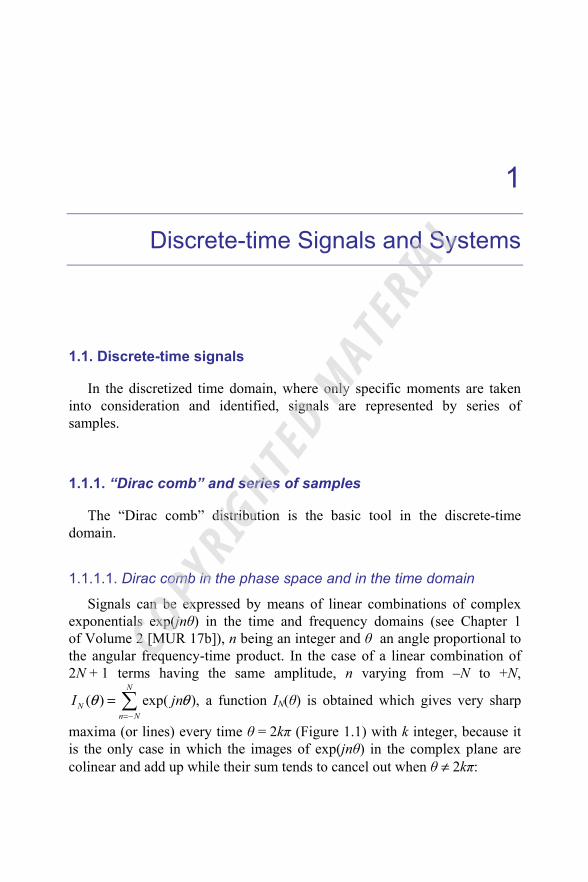
Signals can be expressed by means of linear combinations of complex exponentials exp(jnθ) in the time and frequency domains (see Chapter 1 of Volume 2 [MUR 17b]), n being an integer and θ an angle proportional to the angular frequency-time product. In the case of a linear combination of 2N + 1 terms having the same amplitude, n varying from –N to +N,
( ) exp( ),N
Nn N
I jnθ θ=−
= a function IN(θ) is obtained which gives very sharp
maxima (or lines) every time θ = 2kπ (Figure 1.1) with k integer, because it is the only case in which the images of exp(jnθ) in the complex plane are colinear and add up while their sum tends to cancel out when θ ≠ 2kπ:
COPYRIG
HTED M
ATERIAL
2 Fundamentals of Electronics 3
Figure 1.1. Function IN(θ) with N = 10
The “Dirac comb” is a series of periodic Dirac impulses and can be defined from IN(θ) by taking the limit for N →∞.
Provided that 0
00
0
sin(2 )lim 2 ( )2T
f tf tf t
π δπ→∞
→
and
)(2
)2sin(2lim0
00
0f
tTfTT
Tδ
ππ →
→∞
(see Chapter 1 and the Appendix in
Volume 2 [MUR 17b]), or more generally )()sin(lim θδθ
θ →
∞→ nnn
n, we
define the “Dirac comb” distribution by means of a sum of Dirac impulses (Figure 1.2):
2 1sin2lim exp( ) lim
2 sin2
N
N Nk n N
N
k jnθ
θδ θθπ
∞
→∞ →∞=−∞ =−
+ − = =
I10(θ)
θ /2π
5 4 3 2 1 0 1 2 3 4 5
0
5
10
15
20

Discrete-time Signals and Systems 3
0 1 2 3 4 5 −5 −4 −3 −2 −1
θ / 2π
( )∞
−∞=−
kkπ
θδ 2 .
Figure 1.2. Dirac comb in the phase space
If θ = 2π f0 t, where 00
1 fT
= is a fixed frequency and t is the time
variable, we obtain, by changing variable in the distribution Σδk, a Dirac comb
in the time domain 00 0 0 0( ) lim exp( 2 )
N
kT Nk n NT T t kT j nf tδ δ π
∞
→∞=−∞ =−
Σ = − = with a
single line whenever f0 t = k (k being an integer), that is t = k T0 (Figure 1.3).
-4T0 -3T0 -2T0 -T0 0 T0 2T0 3T0 4T0 5T0
t
Figure 1.3. Time “Dirac comb” distribution of time period T0
00 kTT δΣ is dimensionless and ΣδkT0 has the dimension of a frequency, in order to preserve the dimension of the function to which the distribution is applied.
1.1.1.2. Frequency Dirac comb
Alternatively, if θ = 2π f T0, where 00
1 Tf
= is a fixed period and f is
the frequency variable, we have a Dirac comb in the frequency domain
4 Fundamentals of Electronics 3
00 0 0 0( ) lim exp( 2 )N
nf Nn k Nf f f n f j k f Tδ δ π
∞
→∞=−∞ =−
Σ = − = with a single line every
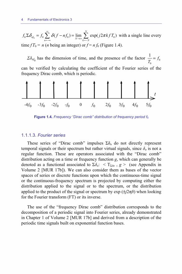
time f T0 = n (n being an integer) or f = n f0 (Figure 1.4).
Σδnf0 has the dimension of time, and the presence of the factor 00
1 fT
=
can be verified by calculating the coefficient of the Fourier series of the frequency Dirac comb, which is periodic.
-4f0 -3f0 -2f0 -f0 0 f0 2f0 3f0 4f0 5f0
t
Figure 1.4. Frequency “Dirac comb” distribution of frequency period f0
1.1.1.3. Fourier series
These series of “Dirac comb” impulses Σδn do not directly represent temporal signals or their spectrum but rather virtual signals, since δn is not a regular function. These are operators associated with the “Dirac comb” distribution acting on a time or frequency function g, which can generally be denoted as a functional associated to Σδn: < TΣδn , g > (see Appendix in Volume 2 [MUR 17b]). We can also consider them as bases of the vector spaces of series or discrete functions upon which the continuous-time signal or the continuous-frequency spectrum is projected by computing either the distribution applied to the signal or to the spectrum, or the distribution applied to the product of the signal or spectrum by exp (±j2πft) when looking for the Fourier transform (FT) or its inverse.
The use of the “frequency Dirac comb” distribution corresponds to the decomposition of a periodic signal into Fourier series, already demonstrated in Chapter 1 of Volume 2 [MUR 17b] and derived from a description of the periodic time signals built on exponential function bases.
Discrete-time Signals and Systems 5
As a matter of fact, by taking the FT of a periodic signal yT0(t) = yT0(t + kT0) in the time domain, then reducing the interval to the period T0 and finally by performing a summation over all periods, we find:
[ ] ( ) [ ]
( ) ( )
0
0
0
0
/2
0 0 0 0/2
/2
0 0/2
TF ( ) ( )exp 2 ( )exp 2 ( )
( )exp 2 exp 2
T
T T TTk
T
TTk
y t y t j f t dt y t j f t kT dt
y t j f t dt j f kT
π π
π π
∞∞
−∞ −=−∞
∞
−=−∞
= − = − +
= − −
expression of the product of the Dirac comb
0 0 0( ) lim exp( 2 )N
Nn k Nf f n f j k f Tδ π
∞
→∞=−∞ =−
− = by the integral between
brackets, to be evaluated for the only line frequencies f = n f0 = 0
nT
. It is
therefore possible to place the result of the integral calculated at f = n f0 inside the summation by replacing f by n f0 and write:
[ ]0 0TF ( ) ( )T nn
y t c f n fδ∞
=−∞
= − with the complex Fourier coefficient
[ ]0
0
/2
0 0/20
1 ( )exp 2T
n TTc y t j n f t dt
Tπ
−= − .
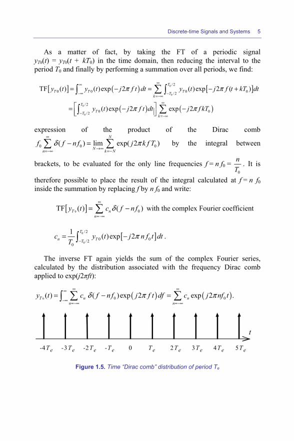
The inverse FT again yields the sum of the complex Fourier series, calculated by the distribution associated with the frequency Dirac comb applied to exp(j2πft):
( ) ( )0 0 0( ) ( )exp 2 exp 2 .T n nn n
y t c f n f j f t df c j nf tδ π π∞ ∞∞
−∞=−∞ =−∞
= − =
-4Te -3Te -2Te -T e 0 Te 2Te 3Te 4Te 5Te
t
Figure 1.5. Time “Dirac comb” distribution of period Te
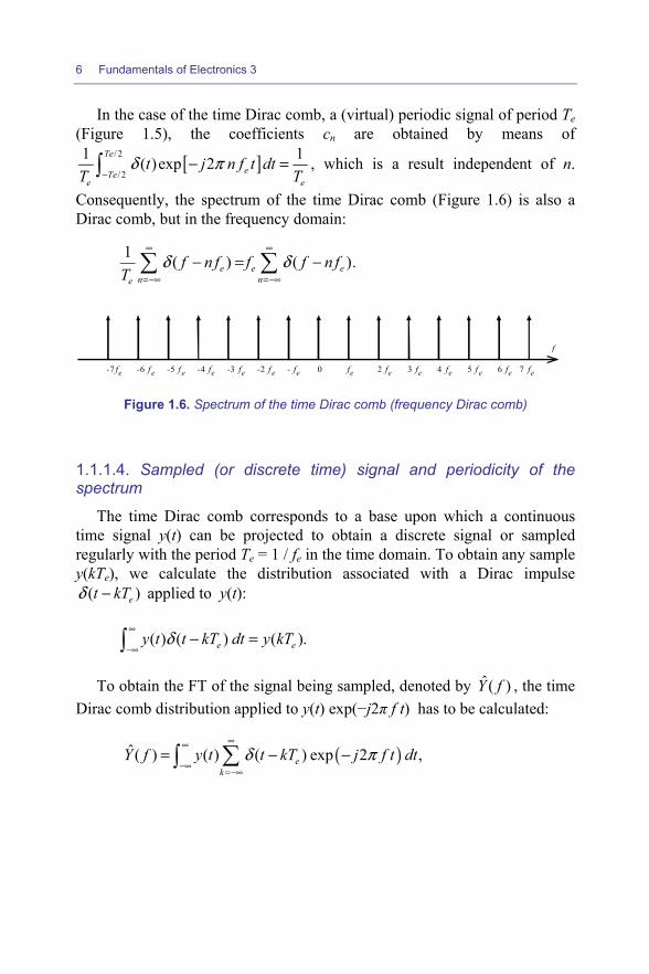
6 Fundamentals of Electronics 3
In the case of the time Dirac comb, a (virtual) periodic signal of period Te (Figure 1.5), the coefficients cn are obtained by means of
[ ]/2
/2
1 1( )exp 2Te
eTee e
t j n f t dtT T
δ π−
− = , which is a result independent of n.
Consequently, the spectrum of the time Dirac comb (Figure 1.6) is also a Dirac comb, but in the frequency domain:
1 ( ) ( ).e e en ne
f n f f f n fT
δ δ∞ ∞
=−∞ =−∞
− = −
-7 fe -6 f e -5 f e -4 fe -3 fe -2 f e - fe 0 fe 2 fe 3 fe 4 fe 5 f e 6 fe 7 fe
f
Figure 1.6. Spectrum of the time Dirac comb (frequency Dirac comb)
1.1.1.4. Sampled (or discrete time) signal and periodicity of the spectrum
The time Dirac comb corresponds to a base upon which a continuous time signal y(t) can be projected to obtain a discrete signal or sampled regularly with the period Te = 1 / fe in the time domain. To obtain any sample y(kTe), we calculate the distribution associated with a Dirac impulse
( )et kTδ − applied to y(t):
( ) ( ) ( ).e ey t t kT dt y kTδ∞
−∞− =
To obtain the FT of the signal being sampled, denoted by ˆ( )Y f , the time Dirac comb distribution applied to y(t) exp(−j2π f t) has to be calculated:
( )ˆ( ) ( ) ( ) exp 2 ,ek
Y f y t t kT j f t dtδ π∞∞
−∞=−∞
= − −
Discrete-time Signals and Systems 7
that is to say, the FT of the regular product ( ) ( )ek
y t t kTδ∞
=−∞
× − . It is thus
the convolution product of the spectrum Y(f) of y(t) by the FT of the time
Dirac comb, which is the frequency Dirac comb ( )e en
f f n fδ∞
=−∞
− , namely:
( )ˆ( ) e e e en n
Y f f nf Y f f Y f nfδ υ υ δυ+∞ +∞ +∞
=−∞ =−∞−∞
= − ( − ) = ( − )
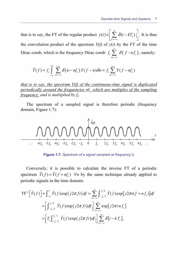
that is to say, the spectrum Y(f) of the continuous-time signal is duplicated periodically around the frequencies nfe, which are multiples of the sampling frequency, and is multiplied by fe.
The spectrum of a sampled signal is therefore periodic (frequency domain, Figure 1.7):
… -6 fe -5 fe -4 fe -3 fe -2 fe - fe 0 fe 2 fe 3 fe 4 fe 5 fe 6 fe …
f
Y(f)
Figure 1.7. Spectrum of a signal sampled at frequency fe
Conversely, it is possible to calculate the inverse FT of a periodic spectrum ˆ ˆ( ) ( )eY f Y f nf= + ∀n by the same technique already applied to periodic signals in the time domain:
( ) [ ]
( ) [ ]
( ) [ ]
/2-1
/2
/2
/2
/2
/2
ˆ ˆ ˆTF ( ) ( )exp 2 ( )exp 2 ( )
ˆ ( )exp 2 exp 2
ˆ ( )exp 2 ,
e
e
e
e
e
e
f
efn
f
efn
f
e efk
Y f Y f j f t df Y f j t f n f df
Y f j f t df j tn f
T Y f j f t df t k T
π π
π π
π δ
∞∞
−∞ −=−∞
∞
−=−∞
∞
−=−∞
= = +
=
= −
8 Fundamentals of Electronics 3
where the integral in brackets only has to be evaluated for the sole moments
tk = kTe = e
kf
where the samples are collected because the time Dirac comb
only contains impulses at times tk.
Therefore, we can put the result of the integral calculated at tk = k Te inside the summation because it then becomes dependent of the index k when t is replaced by tk:
-1 ˆˆ( ) TF ( ) ( ),k ek
y t Y f y t kTδ∞
=−∞
= = −
which is a series of samples of value yk with /2
/2
1 ˆ( )exp 2 .e
e
f
k fe e
fy Y f j k dff f
π−
=
Conclusion: the time signal whose FT is periodic in the frequency domain is a sampled signal (or discrete) in the time domain.
1.1.2. Sampling (or Shannon’s) theorem, anti-aliasing filtering and restitution of the continuous-time signal using the Shannon interpolation formula
If the spectrum Y(f) of the continuous time signal y(t) has a bounded support smaller than [−fe/2, +fe/2], namely equal to 0 outside of an interval
narrower than [−fe/2, +fe/2], ˆ( ) e en
Y f f Y f nf+∞
=−∞
= ( − ) can be replaced by
fe Y(f) between the bounds of the integration interval [−fe/2, +fe/2] in the previous computation of yk with an upper bound fmax < fe/2:
( ) ( )max
max
/2
/2
1 ˆ( )exp 2 ( )exp 2 ( ).e
e
f f
k e e ef fe
y Y f j f kT df Y f j f kT df y kTf
π π− −
= = =
Nonetheless, in the case of a bounded spectrum in the interval [−fmax, +fmax], itself included in the interval [−fe/2, +fe/2], (Figure 1.8),

Discrete-time Signals and Systems 9
( )dfTkfjfYf
fe−
max
max
2exp)( π can be replaced by
( )( )exp 2 eY f j f kT dfπ∞
−∞ , the inverse FT of Y(f) evaluated at times kTe or still the amplitude yk of the samples. We can deduce the sampling (or Shannon’s) theorem:
If a signal y(t), whose spectrum Y(f) is 0 outside [−fmax fmax], is sampled with a sampling rate fe twice larger than the bound fmax, the samples calculated by the inverse transform of the spectrum ˆ( )Y f of the sampled signal ˆ( )y t coincide with the values of the continuous-time signal y(t) evaluated at sampling times tk = kTe.
In the frequency domain, this leads us to state that:
The spectrum of the original signal is preserved after sampling in the interval [−fe/2, +fe/2] provided that it is bounded by a frequency fmax smaller than fe/2, corresponding to the condition: fe > 2 fmax.
f
−4fe −3fe −2fe −fe 0 fe 2fe 3fe 4fe
)(ˆ fY fe Y(f)
−fe/2 −fmax fmax fe/2
Figure 1.8. Spectrum of a sampled signal which follows the Shannon theorem
Conversely, if Shannon’s theorem is not followed, the spectrum ˆ( ) e e
nY f f Y f nf
+∞
=−∞
= ( − ) , which is a sum of all the spectra of the continuous-
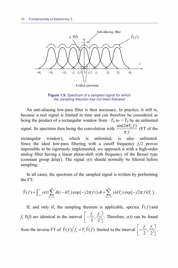
time signal shifted by nfe, exhibits in the interval [−fe/2, +fe/2] at least part of the spectrum Y(f ± fe) usually referred to as the aliased part (Figure 1.9):
10 Fundamentals of Electronics 3
f
−4fe −3fe −2fe −fe −fe/2 0 fe/2 fe 2fe 3fe 4fe
)(ˆ fY fe Y(f)
Anti-aliasing filter
Folded spectrum
Figure 1.9. Spectrum of a sampled signal for which the sampling theorem has not been followed
An anti-aliasing low-pass filter is then necessary. In practice, it still is, because a real signal is limited in time and can therefore be considered as being the product of a rectangular window from −T0 to + T0 by an unlimited
signal. Its spectrum then being the convolution with 0sin(2 )T ff
ππ
(FT of the
rectangular window), which is unlimited, is also unlimited. Since the ideal low-pass filtering with a cutoff frequency fe/2 proves impossible to be rigorously implemented, we approach it with a high-order analog filter having a linear phase-shift with frequency of the Bessel type (constant group delay). The signal y(t) should normally be filtered before sampling.
In all cases, the spectrum of the sampled signal is written by performing the FT:
( ) ( )ˆ( ) ( ) ( ) exp 2 ( ) exp 2 .e e ek k
Y f y t t kT j f t dt y kT j f kTδ π π∞ ∞∞
−∞=−∞ =−∞
= − − = −
If, and only if, the sampling theorem is applicable, spectra ˆ( )Y f and
fe Y(f) are identical in the interval ,2 2
e ef f − . Therefore, y(t) can be found
from the inverse FT of ˆ ˆ( ) ( )e eY f f T Y f= limited to the interval ,2 2
e ef f − ,
Discrete-time Signals and Systems 11
which is tantamount to implementing an ideal time-continuous low-pass
filtering of the signal sampled at the cutoff frequency 2
ef , of transmittance
zero outside ,2 2
e ef f − :
( ) ( )
[ ]
2
2
2
2
( ) ( ) exp 2 exp 2
( ) exp 2 ( ) ,
e
e
e
e
f
e e efk
f
e e efk
y t T y kT j f kT j f t df
T y kT j f t kT df
π π
π
∞
−=−∞
∞
−=−∞
= −
= −
which finally delivers the Shannon interpolation formula:
[ ]sin ( )( ) ( ) .
( )e e
ek e e
f t kTy t y kT
f t kTπ
π
∞
=−∞
−=
−
Remarkable conclusion: it is theoretically possible to recover the time-continuous signal y(t) at any time t, merely from its samples y(kTe), if the sampling theorem can be applied; this requires knowledge of all the samples prior and after time t, considered with a decreasing weight when |t − kTe| increases.
This is achievable by means of numerical computation (samples digitized and stored; see section 1.4.7) but with a finite number of samples in practice; it further enables the interpolation to be achieved by oversampling (2m −1 additional samples calculated between each original samples, rejecting the sampling frequency at 2m fe).
1.1.3. Discrete Fourier series (or transform); “fast Fourier transform” (FFT) and discrete cosine transforms (DCT)
It is assumed that the signal y(t) is sampled N times over a period T0 = 1/f0, which is considered to be the period of the signal. The resulting
signal is periodic and sampled with sampling period NT
Te0= (Figure 1.10):
12 Fundamentals of Electronics 3
0 Te T0=NTe 2T0 3T0 4T0
t
yk
Figure 1.10. Sampled periodic signal
The spectrum is thus discrete and periodic of period 0ef N f= in the frequency domain. In order to obtain the “discrete Fourier transform”, we calculate the coefficients Yn of the Fourier series decomposition of Te y(t) which has been sampled or, in other words, multiplied by a Dirac comb
( )ek
t kTδ∞
=−∞
− , over a time period T0 = NTe:
0 1 10
0 00 00
1 2 1 2exp exp ,T Ν Ν
n e ek k
T nt knY t kT y t j dt y(kT ) jT N Τ N Ν
π πδ− −
= =
= ( − ) ( ) − = −
which represents the complex amplitude of the spectrum line of y(t) sampled
at frequency 00
ee
n n nn f fT NT N
= = = and periodic of frequency period fe.
The spectrum can thus be written as −
=)−(
1
0
N
nen f
NnfY δ when limited
to an interval [0 fe], (Figure 1.11).
−2fe −fe 0 fe/N fe 2fe
f
Yn
Figure 1.11. (Discrete and periodic) spectrum of a sampled
and periodic signal (fast Fourier transform assumption)

Discrete-time Signals and Systems 13
We can even restrict ourselves to N/2 lines because given that y(t) is real, |Yn| is even and Arg{Yn} is odd; Yn can thus be deduced in all other frequency half-periods, especially from −fe/2 to 0 and from fe/2 to fe.
We can calculate the inverse discrete transform of spectrum Yn limited to the frequency period fe, since the spectrum is periodic, in order to find the time samples:
( )1 1
0 00
exp 2 exp 2ef N N
n e e nn n
n knY f f j kT f Y jN N
δ π π− −
= =
( − ) =
.
Hence, finally, the pair of discrete Fourier series can be written as follows by establishing that y[k] = y(kTe) and Y[n] = Y(nfe) = Yn:
1
0
1
0
1[ ] [ ] exp 2
[ ] [ ] exp 2
N
k
N
n
knY n y k jN N
kny k Y n jN
π
π
−
=
−
=
= −
=
These expressions can be computed by an algorithm that makes use of the symmetry properties of exponentials (fast Fourier transform, abbreviated by FFT) and are very often available in digital oscilloscopes. A time window is normally required to limit the discontinuity between the first and the last time samples, which exists due to the quasi-systematic lack of true periodicity. In effect, without a window, this discontinuity introduces a modification in the spectrum. The most used windows are the Hanning
−−=
12cos
21
21
Nnπ , the Hamming 20.54 0.46cos
1n
Nπ = − −
windows,
those with a flat-top from n = N/4 to 3N/4 showing a decrease on both sides
of the peak, the Blackmann 2 40.42 0.5cos 0.08cos1 1n n
N Nπ π = − − − −
or still the triangular windows; moreover, the rectangular window does not bring any change (windowing is covered in more detail in sections 1.4.4.1 and 1.4.6.5).
14 Fundamentals of Electronics 3
There are other existing spectrum calculations, in which complex exponentials are replaced by cosines (from DCT-I to DCT-IV). They make it possible to better “focus” the spectrum in low frequencies; they still take advantage of computational methods using fast algorithms and lend themselves better to data compression by way of truncating the spectrum in higher frequencies. In addition, one way of solving the discontinuity problem between samples of ranks 0 and N-1, much less damaging to the integrity of the signal, is based on the discrete MDCT (Modified Discrete Cosine Transform) which employs twice the number of samples:
2 1
0
1 1[ ] [ ]cos2 2 2
N
k
NY n y k k nNπ−
=
= + + + for n ∈ [0, N–1].
The inverse IMDCT transformation (Inverse Modified Discrete Cosine Transform) allows us to find 2N samples, using the expression:
1
0
1 1 1[ ] [ ]cos2 2 2
N
n
Ny k Y n k nN N
π−
=
= + + + for k ∈ [0, 2N–1].
This type of method provides a means to manage continuously streaming data, such as audio streams, or those with redundant samples, and also to store them in their spectral form after compression or to reproduce the compressed data as a function of the time index (treatments used in MPEG protocols, an abbreviation of “Moving Picture Experts Group”, like MPEG-II, more commonly known as “mp3”).
1.2. Discrete time–continuous time interface circuits
Since one of the terminations of these circuits receives or generates continuous-time signals, the analytical methods are here again the FT and the Laplace transform.
1.2.1. Real sampler
A real sampler has a non-zero sampling time αTe , equal to a fraction α of the sampling period Te = 1/fe (0< α <1) and can be represented by the following schematics (Figure 1.12):
Discrete-time Signals and Systems 15
u(t) q(t)
û(t) R
q(t) 1 0
Te
α Te
1 0
t
Figure 1.12. Simple sampler and its control signal
The clock signal q(t) controls the real sampler. Its spectrum Q(f) is shown in Figure 1.13, together with that of the input signal, assumed to verify the sampling theorem condition.
Q(f)
f −fmax 0 fmax f −5fe −3fe − fe 0 fe 2fe 4fe 6fe …
U(f)
Figure 1.13. Spectra of the control signal and of the signal before the sampler,
assumed to comply with Shannon’s theorem condition fmax < fe/2
It should be noted that the actual sampler shows an impulse response which is none other than the only rectangular pulse of q(t) located between 0 and Te and that the series of impulses observed in q(t) is nothing other than the response of the actual system to a Dirac comb characteristic of ideal

16 Fundamentals of Electronics 3
sampling, which would have been presented on input. The spectrum of the
ideally sampled signal ( ) e en
Û f f U f nf+∞
=−∞
= ( − ) is then simply multiplied by
the FT of this impulse response, which can be calculated as follows:
[ ] [ ] [ ]/2
0 /2exp 2 exp exp 2 ' 'e e
e
T T
e e e Tf j f t dt f j f T j f t dt
α α
απ π α π
−− = − −
[ ] [ ]sin( ) exp sinc( )expee e e
e
f T j f T f T j f Tf T
π αα π α α π α π απ α
= − = − , which finally
gives for the spectrum of the real sampled signal:
[ ]( ) sinc expe e en e
fÛ f f U f nf j f Tf
α π α π α+∞
=−∞
= ( − ) −
.
f
−4fe −3fe −2fe −fe 0 fe 2fe 3fe 4fe
Û(f)
ee f
ff παα sinc
Figure 1.14. Spectrum of the real sampled signal
The spectrum Û(f) of û(t) is no longer periodic (Figure 1.14) but it can be observed that it is still required that the spectrum of u(t) be bounded by a frequency fmax< fe/2 if we want to avoid spectral aliasing and if we want to be able to recover the original signal using simple low-pass filtering. The sampling theorem therefore applies in the same way as for the ideally sampled signal.
The components of the spectrum located around the multiples of the
sampling frequency fe are attenuated by the factor since
ff
α π
with

Discrete-time Signals and Systems 17
respect to that located in the neighborhood of f = 0. The factor [ ]exp ej f Tπ α− corresponds to the introduction of a delay αTe/2, which is
half the sampling duration.
1.2.2. Sample-and-hold circuit
In many cases, the sampler is replaced by a sample-and-hold circuit, either deliberately in order to leave the data during the entire period Te at the input of a digital system or because the system works in a sequential fashion and stores data during one clock period, as is often the case in a digital-to-analog converter (DAC) just before the conversion step. It is thus a function capable of operating both on input and on output of a digital system, functioning as an interface between discrete-time and continuous-time signals. It can be described by a sampler in which the resistance R of the previous schematics has been replaced by a capacitance C, which acts as analog memory (Figure 1.15). It is charged at the new sampled value of the input signal at each period Te and maintains this charge during the entire period Te. The sampled-and-held signal is thus deduced from the previous one by giving α the value of 1, which allows its spectrum to be immediately obtained by replacing α by 1 in the expression of Û(f) of the preceding section.
u(t) q(t) sb(t)
C
q(t)
10
0 Te
10
t
Figure 1.15. Sample-and-hold circuitry and its control signal
The practical implementation of sample-and-hold circuitry requires a voltage source before capacitance C and a follower of infinite input impedance so that the capacitor does not discharge when the switch is open.
18 Fundamentals of Electronics 3
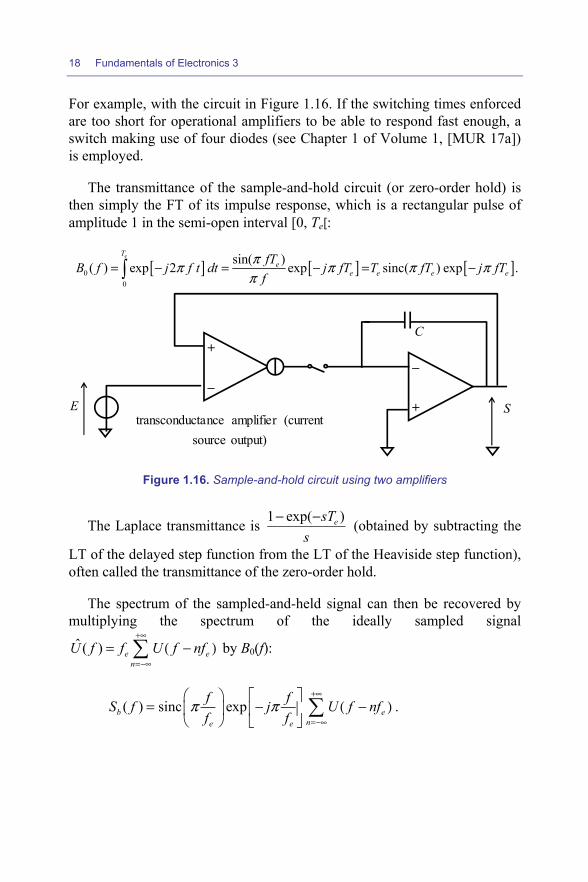
For example, with the circuit in Figure 1.16. If the switching times enforced are too short for operational amplifiers to be able to respond fast enough, a switch making use of four diodes (see Chapter 1 of Volume 1, [MUR 17a]) is employed.
The transmittance of the sample-and-hold circuit (or zero-order hold) is then simply the FT of its impulse response, which is a rectangular pulse of amplitude 1 in the semi-open interval [0, Te[:
[ ] [ ] [ ]00
sin( )( ) exp 2 exp sinc( ) exp .eT
ee e e e
fTB f j f t dt j fT T fT j fTf
ππ π π ππ
= − = − = −
S E
C
transconductance amplifier (current source output)
− +
+ −
Figure 1.16. Sample-and-hold circuit using two amplifiers
The Laplace transmittance is 1 exp( )esTs
− − (obtained by subtracting the
LT of the delayed step function from the LT of the Heaviside step function), often called the transmittance of the zero-order hold.
The spectrum of the sampled-and-held signal can then be recovered by multiplying the spectrum of the ideally sampled signal ˆ ( ) e e
nU f f U f nf
+∞
=−∞
= ( − ) by B0(f):
( ) sinc expb ene e
f fS f j U f nff f
π π+∞
=−∞
= − ( − )
.
Discrete-time Signals and Systems 19
f
−4fe −3fe −2fe −fe 0 fe 2fe 3fe 4fe
Û (f)
f
−4fe −3fe −2fe −fe 0 fmax fe 2fe 3fe 4fe
Spectrum of the sampled-and-held signal Sb(f)
effπsinc
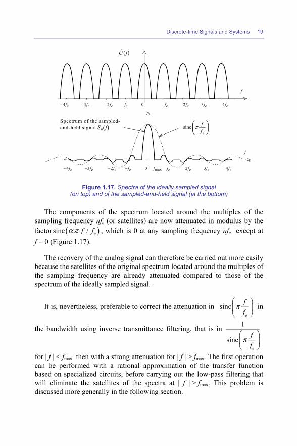
Figure 1.17. Spectra of the ideally sampled signal
(on top) and of the sampled-and-held signal (at the bottom)
The components of the spectrum located around the multiples of the sampling frequency nfe (or satellites) are now attenuated in modulus by the factor ( )sinc / ef fα π , which is 0 at any sampling frequency nfe except at f = 0 (Figure 1.17).
The recovery of the analog signal can therefore be carried out more easily because the satellites of the original spectrum located around the multiples of the sampling frequency are already attenuated compared to those of the spectrum of the ideally sampled signal.
It is, nevertheless, preferable to correct the attenuation in since
ff
π
in
the bandwidth using inverse transmittance filtering, that is in 1
since
ff
π
for | f | < fmax then with a strong attenuation for | f | > fmax. The first operation can be performed with a rational approximation of the transfer function based on specialized circuits, before carrying out the low-pass filtering that will eliminate the satellites of the spectra at | f | > fmax. This problem is discussed more generally in the following section.
20 Fundamentals of Electronics 3
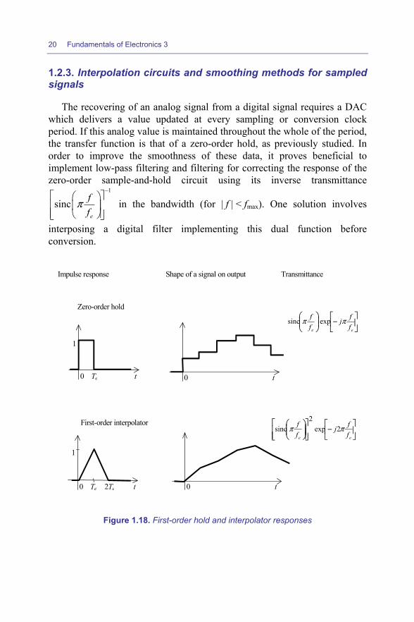
1.2.3. Interpolation circuits and smoothing methods for sampled signals
The recovering of an analog signal from a digital signal requires a DAC which delivers a value updated at every sampling or conversion clock period. If this analog value is maintained throughout the whole of the period, the transfer function is that of a zero-order hold, as previously studied. In order to improve the smoothness of these data, it proves beneficial to implement low-pass filtering and filtering for correcting the response of the zero-order sample-and-hold circuit using its inverse transmittance
1
since
ff
π−
in the bandwidth (for | f | < fmax). One solution involves
interposing a digital filter implementing this dual function before conversion.
0 Te t
Impulse response Shape of a signal on output Transmittance
1
0 t
0 Te 2Te t
1
Zero-order hold
0 t
First-order interpolator
−
ee ffj
ff ππ expsinc
−
ee ffj
ff ππ 2exp
2sinc
Figure 1.18. First-order hold and interpolator responses
Discrete-time Signals and Systems 21
Another solution involves using a kth-order interpolator sampler of
transmittance1
sinck
e
ff
π+
. In the time domain, this filtering achieves
interpolation-based smoothing of the output signal of the sample-and-hold circuit, which is a step function. The corresponding impulse responses are inferred from that of the zero-order hold using time convolution, because raising a transfer function to the k +1 power in the frequency domain corresponds to the k successive convolutions of the initial impulse response
h0(t) in the time domain: 1 0 01( ) ( ) ( )e
h t h h t dT
τ τ τ+∞
−∞
= − ;
2 0 11( ) ( ) ( )e
h t h h t dT
τ τ τ+∞
−∞
= − ; 3 1 11( ) ( ) ( )e
h t h h t dT
τ τ τ+∞
−∞
= − , etc. From h0(t), a
rectangular pulse equal to 1 between 0 and Te, these impulse responses then become a triangle (Figure 1.18), arcs of parabolas, arcs of third, forth-degree polynomial functions and so on. The number of segments is k +1, and the impulse response has a total duration (k +1)Te.
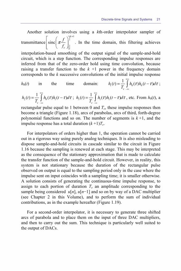
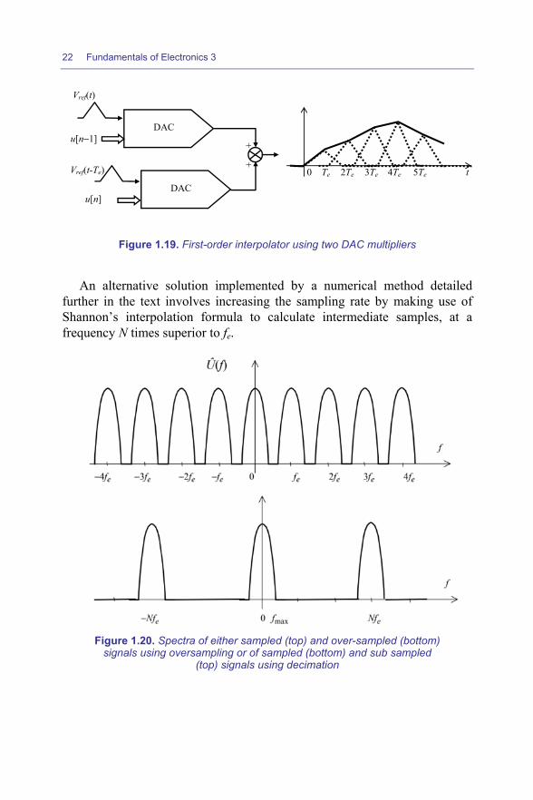
For interpolators of orders higher than 1, the operation cannot be carried out in a rigorous way using purely analog techniques. It is also misleading to dispose sample-and-hold circuits in cascade similar to the circuit in Figure 1.16 because the sampling is renewed at each stage. This may be interpreted as the consequence of the stationary approximation that is made to calculate the transfer function of the sample-and-hold circuit. However, in reality, this system is not stationary because the duration of the rectangular pulse observed on output is equal to the sampling period only in the case where the impulse sent on input coincides with a sampling time; it is smaller otherwise. A solution consists of generating the continuous-time impulse response, to assign to each portion of duration Te an amplitude corresponding to the sample being considered u[n], u[n−1] and so on by way of a DAC multiplier (see Chapter 2 in this Volume), and to perform the sum of individual contributions, as in the example hereafter (Figure 1.19).
For a second-order interpolator, it is necessary to generate three shifted arcs of parabola and to place them on the input of three DAC multipliers, and then to carry out the sum. This technique is particularly well suited to the output of DACs.
22 Fundamentals of Electronics 3
0 Te 2Te 3Te 4Te 5Te t
DAC
DAC
Vref(t)
u[n−1]
Vref(t-Te)
u[n]
+
+
Figure 1.19. First-order interpolator using two DAC multipliers
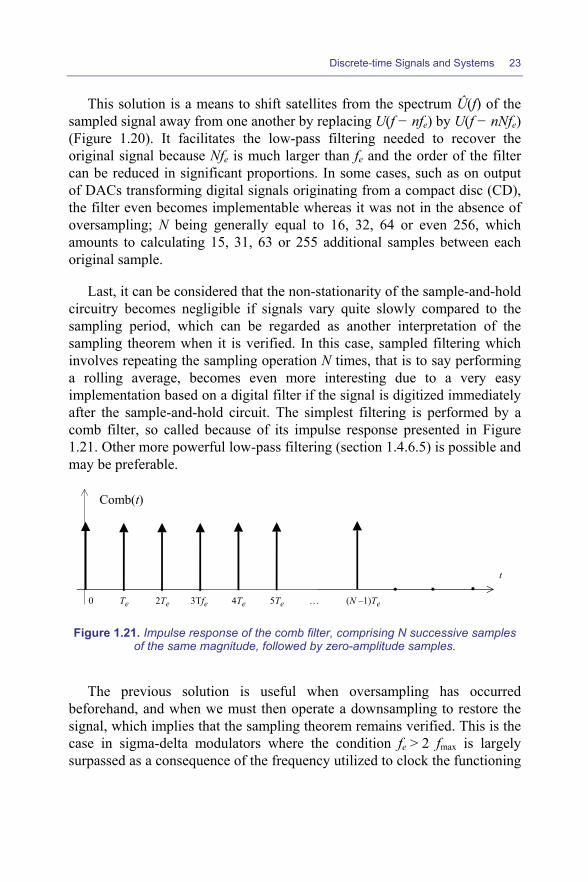
An alternative solution implemented by a numerical method detailed further in the text involves increasing the sampling rate by making use of Shannon’s interpolation formula to calculate intermediate samples, at a frequency N times superior to fe.
Figure 1.20. Spectra of either sampled (top) and over-sampled (bottom) signals using oversampling or of sampled (bottom) and sub sampled
(top) signals using decimation
Discrete-time Signals and Systems 23
This solution is a means to shift satellites from the spectrum Û(f) of the sampled signal away from one another by replacing U(f − nfe) by U(f − nNfe) (Figure 1.20). It facilitates the low-pass filtering needed to recover the original signal because Nfe is much larger than fe and the order of the filter can be reduced in significant proportions. In some cases, such as on output of DACs transforming digital signals originating from a compact disc (CD), the filter even becomes implementable whereas it was not in the absence of oversampling; N being generally equal to 16, 32, 64 or even 256, which amounts to calculating 15, 31, 63 or 255 additional samples between each original sample.
Last, it can be considered that the non-stationarity of the sample-and-hold circuitry becomes negligible if signals vary quite slowly compared to the sampling period, which can be regarded as another interpretation of the sampling theorem when it is verified. In this case, sampled filtering which involves repeating the sampling operation N times, that is to say performing a rolling average, becomes even more interesting due to a very easy implementation based on a digital filter if the signal is digitized immediately after the sample-and-hold circuit. The simplest filtering is performed by a comb filter, so called because of its impulse response presented in Figure 1.21. Other more powerful low-pass filtering (section 1.4.6.5) is possible and may be preferable.
t
0 Te 2Te 3Tfe 4Te 5Te … (N –1)Te
Comb(t)
Figure 1.21. Impulse response of the comb filter, comprising N successive samples of the same magnitude, followed by zero-amplitude samples.
The previous solution is useful when oversampling has occurred beforehand, and when we must then operate a downsampling to restore the signal, which implies that the sampling theorem remains verified. This is the case in sigma-delta modulators where the condition fe > 2 fmax is largely surpassed as a consequence of the frequency utilized to clock the functioning

24 Fundamentals of Electronics 3
of the 1-bit DAC (see Chapter 2), of a factor N much higher than 100. The digital system that processes the flow of 1-bit encoded data on output of the sigma-delta modulator implements both low-pass filtering which is necessary to attenuate the conversion noise as well as the transcoding of 1-bit-encoded data toward n-bit encoding. These techniques are discussed in more detail in section 1.4.7 and in Chapter 2. They allow us to improve the basic “decimation” operation, which simply consists of taking a single sample out of N. Since such an operation is accompanied by a decrease in the sampling frequency with the same ratio N, this represents a subsampling which involves a possible overlapping of the original spectrum with the satellites depicted at the top of Figure 1.20 in the frequency domain if those depicted at the bottom of this same figure are too close to the portion of the spectrum centered on the zero frequency. As a conclusion, the validity of Shannon’s theorem has to be verified every time the sampling frequency is changed, especially when it is downscaled.
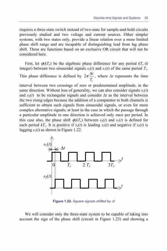
1.3. Phase-shift measurements; phase and frequency control; frequency synthesis
Sample-and-hold circuits are fundamental for measuring the phase shift between two signals, and they provide a basis for phase shift and frequency control and modulation systems, as well as for frequency synthesis systems. Measurement requires a minimal duration of observation of a time period and as such, the resulting signal is a discrete time signal. Nevertheless, as long as the quantities involved in the circuits being used are electric currents and voltages, and because the frequency of the signal is the same as that of the phase shift measurement, the sampling theorem is not necessarily verified. This restriction may, however, be lifted later on (section 1.4.3.3 and section 1.4.5). As a first step, an adequate solution to carry out the analysis then involves using a continuous-time approximation of the response of the sample-and-hold circuit.
1.3.1. Three-state circuit for measuring the phase shift
The basic circuit should allow us to obtain a linear relation between the voltage or the output current and the phase shift existing between two signals, and this should hold even when the phase shift changes sign. This
Discrete-time Signals and Systems 25
requires a three-state switch instead of two-state for sample-and-hold circuits previously studied and two voltage and current sources. Other simpler systems, with two states only, provide a linear relation over a more limited phase shift range and are incapable of distinguishing lead from lag phase shift. These are functions based on an exclusive OR circuit that will not be considered here.
First, let ϕ(kTe) be the algebraic phase difference for any period kTe (k integer) between two sinusoidal signals s2(t) and s1(t) of the same period Te.
This phase difference is defined by 2e
tT
π Δ , where Δt represents the time
interval between two crossings of zero or predetermined amplitude, in the same direction. Without loss of generality, we can also consider signals s1(t) and s2(t) to be rectangular signals and consider Δt as the interval between the two rising edges because the addition of a comparator to both channels is sufficient to obtain such signals from sinusoidal signals, or even for more complex alternative signals; at least in the case in which the passage through a particular amplitude in one direction is achieved only once per period. In this case also, the phase shift ϕ(kTe) between s2(t) and s1(t) is defined for each period kTe. It is positive if s2(t) is leading s1(t) and negative if s2(t) is lagging s1(t) as shown in Figure 1.22.
s1(t)
0 Te 2 Te 3Te t
t
s2(t)
Δt
Figure 1.22. Square signals shifted by Δt
We will consider only the three-state system to be capable of taking into account the sign of the phase shift (circuit in Figure 1.23) and showing a

26 Fundamentals of Electronics 3
linear response range π2± [CD 4046]. In this circuit, the switches K1 and K2 are controlled by the time step Δt: K2 or K1 is in position 1 (or H) during Δt depending on whether the phase ϕ is respectively positive (phase lead) or negative (phase lag); K1 and K2 are in zero position (or L) outside the interval of duration Δt between edges of the same direction.
Figure 1.23. Circuit for measuring the integral of the phase shift between square signals, controlled by the binary signals K1 and K2,
either one being 1 during Δt according to the sign of ϕ
The three states thus correspond to: (1) C0 charged by the constant current I0 during the time interval Δt, if ϕ is positive; (2) C0 discharged by the constant current I0 during the time interval Δt, if ϕ is negative; (3) C0 preserving the charge acquired during the remaining time interval when the
two switches are in position 0. By replacing Δt by2eT ϕπ
, we have the
following recurrence relation: uϕ(kTe) = uϕ [(k−1)Te] + 0
0 2eI TC
ϕπ
.
The increase in voltage 0
0 2eI TC
ϕπ
results from the charging (or
discharging) of the capacitor during a fraction Δt of the period, figured by the solid line in Figure 1.24:

Discrete-time Signals and Systems 27
uϕ(t)
0 Te 2 Te 3Te 4Te 5Te 6Te t
Δt
ϕ > 0 ϕ < 0
Figure 1.24. Signal output of the circuit for measuring the integral phase shift (solid line) and its continuous-time approximation (dotted line)
This increase is indeed proportional to the phase shift ϕ, regardless of its sign. Since the sample period Te merges with the period of electric signals s1(t) and s2(t), the sampling theorem is not verified. The most fruitful approximation then involves replacing the actual variation shown with a solid line in Figure 1.24 by the dashed-line segments that join the values of uϕ(kTe) at each time kTe, which amounts to replacing uϕ(kTe) by
0
0
( ) ( )2
Iu t t dtCϕ ϕ
π= , which is obtained by integrating 0
0
( )2
I tC
ϕπ
that is
to say the slope of each segment. This is all the more justified that the capacitance plays the role of integrator, and that there is no zero resetting of its charge at each period. It thus keeps the memory of the previous phase shifts, which corresponds to integration in the continuous-time domain. In the event it is desirable to change the sign of the relation between the phase comparator input and output signals, it suffices to change the connection of the capacitance C0 at the polarization source Vmin and to replace it with a connection to the polarization source Vmax.
Since this approximation consists of replacing the discrete time variable kTe by the continuous-time variable t, it also makes it possible to assimilate ϕ(t) with the instantaneous phase of a sinusoidal signal s(t) = sin[ϕ(t)], for example, or with the modulated phase shift ϕm(t) of a fixed-frequency signal sin[2π f0 t + ϕm(t)], and therefore to consider all quantities as if they were dependent on the continuous time t.
The control of switches K1 and K2 is achieved based on a sequential logical system making use of synchronous positive-edge triggered D flip-

28 Fundamentals of Electronics 3
flops (Figure 1.25). A typical circuit is the phase-shift detector no.2 of the 4046-based phase-locked loop (PLL) using CMOS technology [CD 4046] because it allows the previously described control for the phase-shift measurement circuit when the frequency of the signals s1(t) and s2(t) is the same.
Figure 1.25. Operation diagram of the control circuit of the phase-shift detector no.2 of the 4046 circuit
In cases where the frequencies are identical, it is shown that the circuit of Figure 1.25 is capable of activating K1 or K2 to state H for the duration Δt according to the sign of the phase shift. For example, in the case of negative phase shift (s2 lagging s1) of Figure 1.26, Q1 first reaches H followed by Q2 after time Δt, while they were at state L previously as it will be shown due to the resetting. During this duration Δt, the output K1 thus shifts to H, while K2 remains L. Then the transition from Q2b to L brings K1 back to L, while K2 remains L, because of Q1b. This normal sequential operation of flip-flops ceases when the transition from Q2 to H is effected, because Q1 is also H at that moment, then the gate U3A causes the resetting of the flip-flops, making Q1, Q2, K1 and K2 shift to L (see Figure 1.26). The opposite applies if s2 is leading s1, which results in the circuits operating as full phase and

Discrete-time Signals and Systems 29
frequency detectors (PFDs) as demonstrated further in the case of non identical input frequencies. The output signals of the U3A gate and of the flip-flop which receives the input signal lagging the other are impulses whose duration is determined by switching and propagation times of the circuits. Their duration can be increased by introducing “buffer” or inverter circuits (in even numbers) between the output of the NAND U3A gate and the reset (/CLR) input of the flip-flops.
s1(t)
t
t s2(t)
Q1(t)
Q2(t)
Δt Δt Δt
t
t
Figure 1.26. Sequence of the input and output signals of the flip-flops in the case of signals with the same frequency and shifted by a lag Δt
In addition, the circuit in Figure 1.25 operates as a frequency detector when the frequencies of s1(t) and s2(t) are different, respectively corresponding to periods T1 and T2. The phase shift can no longer be defined but it is always possible to reason based on the interval Δt between two rising edges of signals s1(t) and s2(t). Assuming that we start with synchronous signals and suddenly increase the frequency of s2(t) for instance, the first rising edge appearing on one of the inputs of the circuit of Figure 1.25 will be that of s2(t) followed on the other input by that of s1(t)
30 Fundamentals of Electronics 3
with a delay Δt = T1 − T2, which will lead to reset (/CLR) the two flip-flop outputs Q1 and Q2 (Figure 1.25) and to stop the capacitance C0 from charging. This process will be repeated with increasing delays 2(T1 − T2), 3(T1 − T2) and so on, until the delay becomes greater than T2 and until the same process resumes starting with minimal delay. Since the charge of the capacitance C0 increases for every duration Δt, uϕ (t) will have had time to reach either the minimal saturation voltage Vmin, or the maximal saturation voltage Vmax. The effect is reversed in the case of a contrary condition on frequencies, which is reflected by the circuit operating as a frequency detector delivering a binary signal with a value depending on the status resulting from the comparison of frequencies.
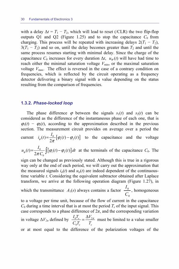
1.3.2. Phase-locked loop
The phase difference ϕ between the signals s1(t) and s2(t) can be considered as the difference of the instantaneous phase of each one, that is ϕ1(t) − ϕ2(t), according to the approximation described in the previous section. The measurement circuit provides on average over a period the
current [ ]01 2( ) ( ) ( )
2= −Ii t t tϕ ϕ ϕ
π to the capacitance and the voltage
[ ]01 2
0
( ) ( ) ( )2
Iu t t t dtCϕ ϕ ϕ
π= − at the terminals of the capacitance C0. The
sign can be changed as previously stated. Although this is true in a rigorous way only at the end of each period, we will carry out the approximation that the measured signals iφ(t) and uφ(t) are indeed dependent of the continuous-time variable t. Considering the equivalent subtractor obtained after Laplace transform, we arrive at the following operation diagram (Figure 1.27), in
which the transmittance A1(s) always contains a factor 0
0
CI
, homogeneous
to a voltage per time unit, because of the flow of current in the capacitance C0 during a time interval that is at most the period Te of the input signal. This case corresponds to a phase difference of 2π, and the corresponding variation
in voltage ΔV2π defined by 0 2
0
e
e e
I T VC T T
πΔ= must be limited to a value smaller
or at most equal to the difference of the polarization voltages of the

Discrete-time Signals and Systems 31
circuits Vmax − Vmin otherwise the risk of introducing non linearity could be incurred, reducing the usable phase-shift range. Most of the time, the value
0 max min
0
e
e e
I T V VC T T
−= will be selected to allow for optimal sensitivity.
However, as discussed further in the text, it proves useful in some cases to decrease the sensitivity, and to this end, we will be able to adopt a smaller ΔV2π value by reducing the ratio I0 / C0.
Figure 1.27. Integrated phase subtractor
The previous circuit diagram can be completed by a correction loop filter making use of a passive network and possibly one or two operational amplifiers, a voltage-controlled oscillator (VCO) of actual transmittance Kf followed possibly by a divide-by-N frequency divider if it is desirable to achieve a closed-loop multiply-by-N frequency multiplier (see Figure 1.28), and a functional block enabling the phase-shift frequency on the VCO output
to be transformed by taking the Laplace transform of0
( ) 2 ( ') 't
t f t dtϕ π= ,
equal to 2sπ F(s) (with f and F being respectively the time dependent
frequency and its LT). The control is then completed by unitary feedback.
In the absence of correction, the loop transmittance would be s-2, with two poles on the imaginary axis, and would lead to an unstable closed-loop system. It is demonstrated that with a first-order phase-lead correction (see exercise 1.6.4), the closed-loop transmittance Hφ(s) is of the second-order with a natural frequency ωn and a damping factor ζ. This natural frequency has to be compared with the frequency variation of the phase or frequency imposed on the system input or with the modulation frequency. The parameters
32 Fundamentals of Electronics 3
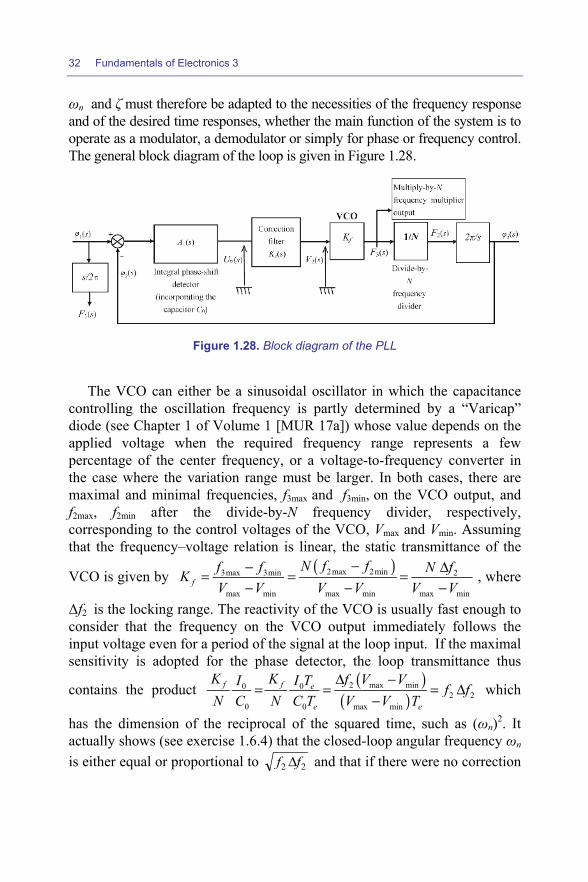
ωn and ζ must therefore be adapted to the necessities of the frequency response and of the desired time responses, whether the main function of the system is to operate as a modulator, a demodulator or simply for phase or frequency control. The general block diagram of the loop is given in Figure 1.28.
Figure 1.28. Block diagram of the PLL
The VCO can either be a sinusoidal oscillator in which the capacitance controlling the oscillation frequency is partly determined by a “Varicap” diode (see Chapter 1 of Volume 1 [MUR 17a]) whose value depends on the applied voltage when the required frequency range represents a few percentage of the center frequency, or a voltage-to-frequency converter in the case where the variation range must be larger. In both cases, there are maximal and minimal frequencies, f3max and f3min, on the VCO output, and f2max, f2min after the divide-by-N frequency divider, respectively, corresponding to the control voltages of the VCO, Vmax and Vmin. Assuming that the frequency–voltage relation is linear, the static transmittance of the
VCO is given by ( )2max 2min3max 3min 2
max min max min max minf
N f ff f N fKV V V V V V
−− Δ= = =− − −
, where
Δf2 is the locking range. The reactivity of the VCO is usually fast enough to consider that the frequency on the VCO output immediately follows the input voltage even for a period of the signal at the loop input. If the maximal sensitivity is adopted for the phase detector, the loop transmittance thus
contains the product ( )( )
2 max min0 02 2
0 0 max min
f f e
e e
K K f V VI I T f fN C N C T V V T
Δ −= = = Δ
− which
has the dimension of the reciprocal of the squared time, such as (ωn)2. It actually shows (see exercise 1.6.4) that the closed-loop angular frequency ωn is either equal or proportional to 22 ff Δ and that if there were no correction
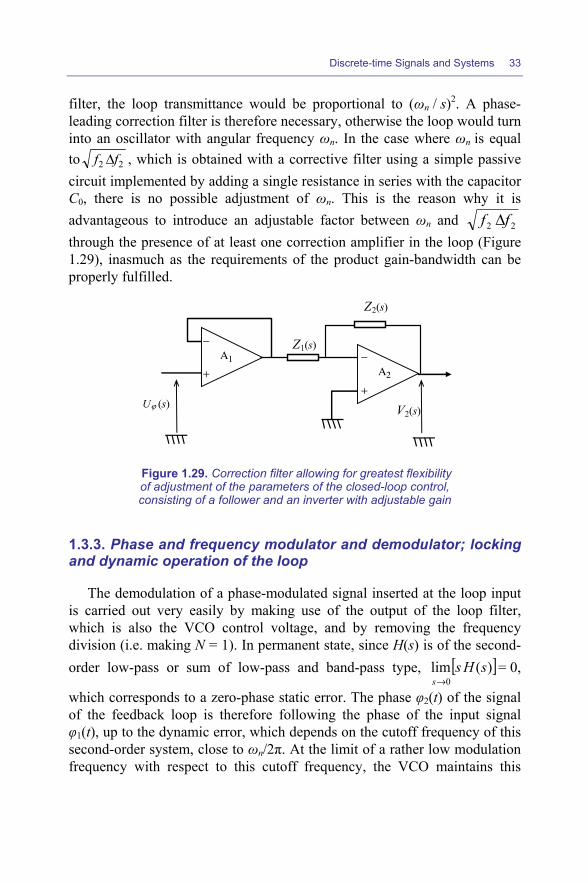
Discrete-time Signals and Systems 33
filter, the loop transmittance would be proportional to (ωn / s)2. A phase-leading correction filter is therefore necessary, otherwise the loop would turn into an oscillator with angular frequency ωn. In the case where ωn is equal to 22 ff Δ , which is obtained with a corrective filter using a simple passive circuit implemented by adding a single resistance in series with the capacitor C0, there is no possible adjustment of ωn. This is the reason why it is advantageous to introduce an adjustable factor between ωn and 22 ff Δ through the presence of at least one correction amplifier in the loop (Figure 1.29), inasmuch as the requirements of the product gain-bandwidth can be properly fulfilled.
− Α2
+
Z1(s)
Z2(s)
V2(s) Uϕ (s)
− Α1 +
Figure 1.29. Correction filter allowing for greatest flexibility of adjustment of the parameters of the closed-loop control, consisting of a follower and an inverter with adjustable gain
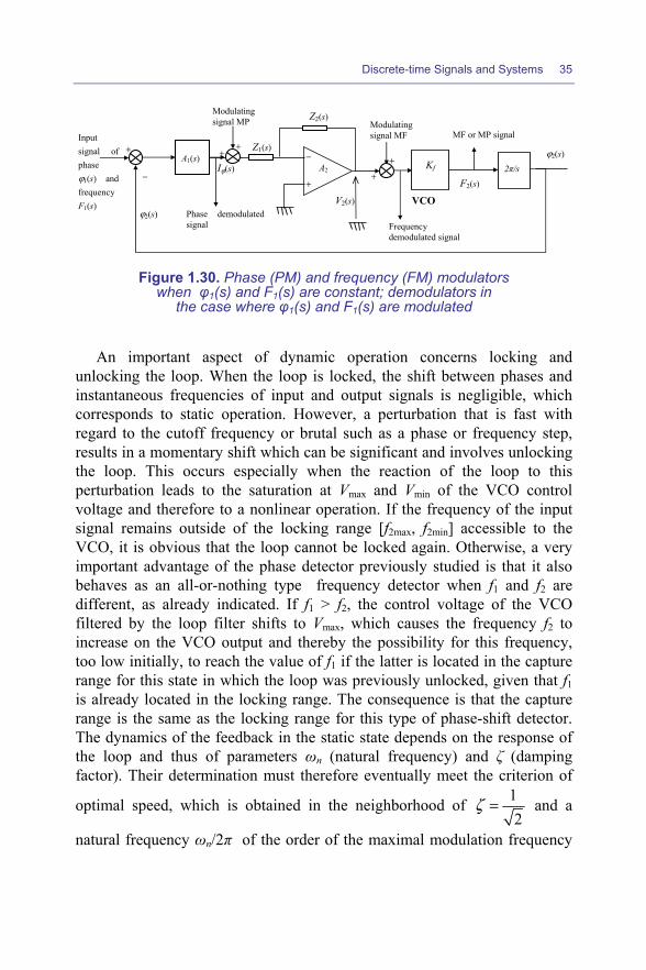
1.3.3. Phase and frequency modulator and demodulator; locking and dynamic operation of the loop
The demodulation of a phase-modulated signal inserted at the loop input is carried out very easily by making use of the output of the loop filter, which is also the VCO control voltage, and by removing the frequency division (i.e. making N = 1). In permanent state, since H(s) is of the second-order low-pass or sum of low-pass and band-pass type, [ ])(lim
0sHs
s→= 0,
which corresponds to a zero-phase static error. The phase φ2(t) of the signal of the feedback loop is therefore following the phase of the input signal φ1(t), up to the dynamic error, which depends on the cutoff frequency of this second-order system, close to ωn/2π. At the limit of a rather low modulation frequency with respect to this cutoff frequency, the VCO maintains this
34 Fundamentals of Electronics 3
phase error close to zero. However, given that relations between phase and
instantaneous frequency are 0
( ) 2 ( ') 't
t f t dtϕ π= and symmetrically
1 ( )( )2
d tf tdtϕ
π= , the VCO control voltage is 2 2( ) 1 ( )
2f f
f t d tK K dt
ϕπ
= . It is
therefore possible to recover the phase modulation following an integrator added after the loop filter (but outside of the loop so as not to modify the correction), which is consistent with the previous fundamental relations. A more economical solution implies directly using an image of this current to enable access to phase modulation; it is feasible insofar as the capacitance C0 plays the role of the integrator of the output current of the phase comparator if the modulation frequency remains low enough compared to the cutoff frequency of the filter correction.
Conversely, in the case where the loop receives a fixed frequency and a fixed phase signal, a phase modulation can be simply introduced by adding a superimposed current to the output current iφ(t) of the phase detector (or its LT Iφ(s) in the block diagram). This solution is very advantageous in situations where the frequency of the signal must remain very stable and accurate in the absence of modulation, as in telecommunication systems, because the sinusoidal source function driven by a quartz oscillator can be separated from the modulation function independently implemented. This method allows for both phase and frequency modulation inasmuch as the signal necessary for the second is deduced from that required for the first by integration.
Similar principles can be applied for direct frequency modulation and demodulation. The feedback voltage is recovered directly on the input of the VCO when the loop input signal is modulated in frequency. Concerning the modulation, a voltage perturbation superimposed onto the VCO control voltage is injected. In fact, it is important to note that the closed-loop transmittance is the same for phase and for frequency because
2 22 1
1 1
( ) ( )( ) ( )( )2 2( ) ( )
s F ss s s sH ss F s
ϕ ϕ ϕπ πϕ
= = = , which is the ratio of the LT of the
phases and the ratio of the LT of the frequencies as well. Consequently, the static frequency error is also zero and the loop dynamically reacts in the same manner to phase and frequency variations.
Discrete-time Signals and Systems 35
− Α2
+
Z1(s)
Z2(s)
Kf
F2(s)
Iϕ(s)
V2(s)
A1(s)
ϕ2(s)
−
+
2π/s
VCO
Input signal of phase ϕ1(s) and frequency F1(s)
ϕ2(s)
MF or MP signal Modulating signal MF
++
+
Frequency demodulated signal
Modulating signal MP
+
Phase demodulated signal
A2
Figure 1.30. Phase (PM) and frequency (FM) modulators when φ1(s) and F1(s) are constant; demodulators in
the case where φ1(s) and F1(s) are modulated
An important aspect of dynamic operation concerns locking and unlocking the loop. When the loop is locked, the shift between phases and instantaneous frequencies of input and output signals is negligible, which corresponds to static operation. However, a perturbation that is fast with regard to the cutoff frequency or brutal such as a phase or frequency step, results in a momentary shift which can be significant and involves unlocking the loop. This occurs especially when the reaction of the loop to this perturbation leads to the saturation at Vmax and Vmin of the VCO control voltage and therefore to a nonlinear operation. If the frequency of the input signal remains outside of the locking range [f2max, f2min] accessible to the VCO, it is obvious that the loop cannot be locked again. Otherwise, a very important advantage of the phase detector previously studied is that it also behaves as an all-or-nothing type frequency detector when f1 and f2 are different, as already indicated. If f1 > f2, the control voltage of the VCO filtered by the loop filter shifts to Vmax, which causes the frequency f2 to increase on the VCO output and thereby the possibility for this frequency, too low initially, to reach the value of f1 if the latter is located in the capture range for this state in which the loop was previously unlocked, given that f1 is already located in the locking range. The consequence is that the capture range is the same as the locking range for this type of phase-shift detector. The dynamics of the feedback in the static state depends on the response of the loop and thus of parameters ωn (natural frequency) and ζ (damping factor). Their determination must therefore eventually meet the criterion of
optimal speed, which is obtained in the neighborhood of 12
=ζ and a
natural frequency ωn/2π of the order of the maximal modulation frequency
36 Fundamentals of Electronics 3
fMmax or preferably greater. Nevertheless, it is necessary to ensure the low-pass filtering of the output signal from the phase-shift detector in an efficient way, which is mainly achieved through the integrating effect due to the capacitance C0. A good trade-off implies taking a value for ωn/2π of at least
max 2minMf f or approximating 2max 2minf f as much as possible. Conversely, if the loop is intended to only recover the carrier frequency of a signal modulated in amplitude, in phase or frequency, but comprising a line at this carrier frequency as is often the case, it will be more effective to decrease the natural frequency ωn/2π and even to increase the damping factor a little in order to reduce the sensitivity of the loop to sidebands due to modulation that can never be completely eliminated by filtering alone. This will be achieved by decreasing the sensitivity of the phase-shift detector, as previously described.
In the case where the PLL is utilized as frequency control, contrary to the previous case, it has to follow abrupt jumps of the input frequency. Its step response is therefore decisive for the agility criterion which characterizes the number of periods after which the output frequency is again equal to that of the input. To decrease this number of periods, we must seek to increase the natural frequency ωn/2π. A very effective solution involves adding an additional correction provided by a derivator to the one including leading phase correction and already implemented (see exercise 1.6.4). Indeed, in this way, the response speed of the loop is improved by the signal derived from uϕ(t) which, injected into the input of the VCO, acts to change its frequency in the same direction as the variation of the input frequency. The total closed-loop response then becomes the sum of those of a low-pass with a band-pass filter and it is possible to significantly increase its natural frequency without compromising its stability (see exercise 1.6.4). It results in locking again on the input frequency after a few periods only (<10), which represents a satisfactory performance in terms of agility of the loop. In addition, it provides a means to respond to the imperatives of the demodulations of phase- or frequency-modulated digital signals and of the frequency synthesis examined later in the text. It is nonetheless unwise to derive a signal that has already been integrated, and moreover the use of a differentiator would cause stability issues, as well as problems of gain-bandwidth product of the operational amplifier that is needed to implement this function in addition to an increase of phase noise of the VCO. It is no longer possible to use the current iϕ(t), which is actually a series of pulses of duration Δt, which cannot be filtered without introducing a prejudicial delay

Discrete-time Signals and Systems 37
to the implementation of the desired transmittance for this correction. The solution then involves generating a signal that is directly proportional to the phase difference of the input signals and not to their integral by adding a sample-and-hold circuit that allows for resetting the charge of the capacitance C0 (Figure 1.31).
Figure 1.31. Circuit for measuring the phase shift between square signals; the impulses CLR1 and CLR2, respectively, control the update of the signal after the
delay Δt and the zeroing
To obtain a signal directly proportional to the phase difference ϕ(kTe) for any period, it suffices to hold its value after the measurement period Δt for the remaining time before the next measurement using the reset impulse of the D flip-flops (/ CLR) of the control circuit (diagram Figure 1.25), which here is renamed CLR1. Next, the charge stored in the capacitance C0 has to be zeroed by way of short-circuiting before the next measurement. For this last operation, the pulse CLR2 has to be generated, shifted by half a period compared to CLR1, employing a control circuit identical to that of Figure 1.25 but implemented by falling-edge triggered flip-flops or still with the same circuit but receiving the inverted signals s1(t) and s2(t). The overall operation may be understood as that of a master–slave analog system based on the alternation of commands CLR1 and CLR2. We thus obtain on the circuit output of Figure 1.31 a signal representing a correct approximation of the derivative uϕ’(t) of the signal uϕ(t) in the context of the continuous-time
uϕ’(t) C0
K2(Δt)if ϕ > 0
Vmax
0 1
I0
0 1
Vmin
I0
K1(Δt)if ϕ < 0
CLR2 CLR1
I2
C3
- Α3+
+ Α2-

38 Fundamentals of Electronics 3
approximation, providing a measure of the phase shift 0
0
( )2e
I tTC
ϕπ
for every
period of the input signal. The optimal sensitivity is obtained as previously when the detector delivers a voltage Vmax − Vmin for a phase shift of π, that
is 0max min
0 2eI T V V
C= − . The transmittance of this phase-shift detector is then
' 0 max min
0 2eI T V VK
Cϕ π π−= = and the loop transmittance without correction
becomes ' max min 2max 2min2 2 2ff
K V V f fK Ks N N s sϕπ − −= = with a characteristic
angular frequency ( )2max 2min2c f fω = − . The smoothing of the edges happening at each update of uϕ’(t) can be adjusted a little with parameters I2 and C3 of the sample-and-hold circuit of Figure 1.31, provided that the duration of the impulse CLR1 is somewhat lengthened as described in section 1.3.1. This signal uϕ’(t) can therefore be used to add a correction branch proportional to the phase shift in the phase control (see exercise 1.6.4). From the point of view of modeling based on a block diagram, this operation is fully equivalent to that consisting of adding a derived correction following the integral phase detector of Figure 1.30 or of its functional block obtained by LT in Figure 1.31.
It is possible to use only the single circuit of Figure 1.31 to measure the phase shift associated to an integral-proportional correction in the PLL. Nonetheless, the addition of further correction as described previously thus becomes more difficult to be implemented and the advantage of the first detector operating as a frequency comparator, which proves very useful when input frequency excursions exceed the locking range, is lost. The latter holds for a rather modest simplification of the circuitry since two logic control systems (Figure 1.25) remain necessary for the generation of the impulses CLR1 and CLR2 in the case of the detector of Figure 1.31. Finally, it is important to note that in the presence of a single proportional correction following this last phase-shift detector, the loop transmittance would be just
( )2max 2min2c f fs s
ω −= , and that accordingly the closed-loop transfer function
would be of the first-order low-pass type cs ω/1
1+
with a cutoff frequency
Discrete-time Signals and Systems 39
equal to ωc. This system is not relevant because it is too inefficient in terms of loop gain error and flexibility of the loop.
1.3.4. Analog frequency synthesis
Frequency synthesis utilizes some functions, all based on PLLs in locked operation, which ensures that the signals on both inputs of the phase comparator have the same frequency. The input signal is most often provided by a quartz oscillator, providing high stability for its frequency and those deduced therefrom. The other circuits needed are mainly simple or specialized mixers, low-pass or bandpass filters and simple or specialized frequency divider-counters. Due to cutoff filters with steep slopes, the spectral purity of the sinusoidal output signal is very good, with a rejection of unwanted frequencies that can reach or exceed 100 dB.
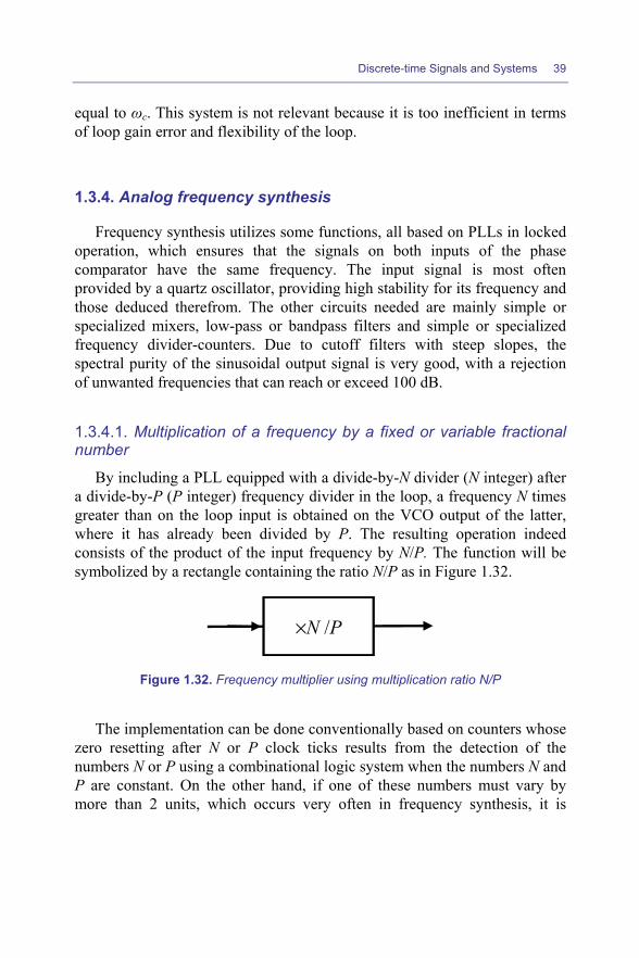
1.3.4.1. Multiplication of a frequency by a fixed or variable fractional number
By including a PLL equipped with a divide-by-N divider (N integer) after a divide-by-P (P integer) frequency divider in the loop, a frequency N times greater than on the loop input is obtained on the VCO output of the latter, where it has already been divided by P. The resulting operation indeed consists of the product of the input frequency by N/P. The function will be symbolized by a rectangle containing the ratio N/P as in Figure 1.32.
×N /P
Figure 1.32. Frequency multiplier using multiplication ratio N/P
The implementation can be done conventionally based on counters whose zero resetting after N or P clock ticks results from the detection of the numbers N or P using a combinational logic system when the numbers N and P are constant. On the other hand, if one of these numbers must vary by more than 2 units, which occurs very often in frequency synthesis, it is

40 Fundamentals of Electronics 3
advantageous to resort to a split counter using division rate switching. A first counter divides by P1 or P2 depending on the value 0 or 1 of a control bit V, which only requires a detection system in which a 2-to-1 multiplexer controlled by V has been added to perform the zero reset command. A second counter placed in cascade after the first one divides by a fixed integer P3. A third circuit carries out the bit-to-bit logic comparison of the word M transmitted to the parallel outputs of the second counter with the instruction word K (<P3) that represents the desired variation for the overall counting rate.
Figure 1.33. Divide-by-P2× P3 + K× (P1 – P2) frequency
It outputs V = 0 if M < K and V = 1 if M ≥ K. The first of both conditions is implemented at the start of the counting and accordingly the first counter divides by P1, which drives the second counter into increasing its outputs by one only after P1 clock ticks on the first counter input. Therefore, on the outputs of the second counter, M reaches the value K after P1 × K clock ticks on the input of the first counter, and then toggles the first counter to shift to a division by P2 rate. Since there is no premature zero reset due to any circuitry for the counters, the second still has to count up to P3 to return to its original state and to this end the first still has to receive P2 × (P3 − K) clock ticks. Subsequently, P1 × K + P2 × (P3 − K) clock ticks are necessary on input in total, or still P2 × P3 + K × (P1 − P2).
Given that it is often desirable that this result be increased by one unity as for K, it suffices to take P1 − P2 = 1, and the other values are determined by the limits that the overall division rate should assume, which can easily exceed 100, and from practical considerations concerning every counter.

Discrete-time Signals and Systems 41
Details of the frequency divider circuit are given in Figure 1.33, while the division function and the multiplication function obtained by inserting the divider in a PLL are symbolized in Figure 1.34.
Figure 1.34. Frequency multiplier on the left and frequency divider on the right, each with unit step for the control number K
Exercise: determine the parameters to obtain a count from 290 to 299.
Answer: If K varies from 0 to 9, we must have P2 × P3 = 290, which is not divisible by a power of 2 except 2. However, if K varies from 2 to 11, P2 × P3 = 288, which is divisible by 32. There is thus interest in choosing this solution with P3 = 32, P1 = 10 and P2 = 9, which implies no combinatorial network or at most an AND gate for the resetting detection.
1.3.4.2. Frequency shift
It is often useful in many systems, especially in telecommunications, to shift an initial frequency f1 of a fixed value or a variable Δf. The simple method previously described which consists of adding a voltage modulation on the VCO input of the PLL may be appropriate if there are no concerns about the loss of accuracy in the value of the frequency which is not any longer only driven by a quartz oscillator. Nonetheless, this disadvantage is generally not tolerable in frequency synthesis.
Figure 1.35. Frequency-shift loop based on the locking condition f1 = f0 – f2 that yields an output VCO frequency f0 = f1 + f2
f1 + f2 f2
× f1 V C O
L o w -p a s sf il te r
-
+ P h a s ec o m p a ra to r a n dc o rre c t io n f i l te r
f0 f0 ± f2
f0 - f2 = f1
M ix e r

42 Fundamentals of Electronics 3
It is however possible to preserve the advantage from the stability provided by the quartz clock-based control by inserting after the VCO a mixer that achieves the product of the output signal of the VCO at frequency f0 by an external signal at frequency f2, followed by a low-pass filter that provides a signal frequency equal to the difference of the frequencies existing on the input of the mixer, namely f0 − f2 (Figure 1.35). Since the loop is locked, the low-pass filter output must be achieved at frequency f1 because it is transmitted back to the input through the feedback loop (it is assumed that there is no division of frequency inside the loop). Consequently, the output frequency of the VCO must be f0 = f1 + f2 so that f1 = f0 − f2 and it suffices to choose Δf = f2, this last frequency being controlled by a quartz oscillator if necessary.
1.3.4.3. Multiplication of a shift between two frequencies
A slightly more complex system than the previous one allows us to make a conversion of frequency using a multiplicative factor which affects the shift Δf1 between the two input frequencies of the system, f0 and f1, close enough, in other words differing at most by a few percentage. It comprises a main loop in which several operations carried out by frequency division and/or multiplication as well as mixer assemblies added to a bandpass filter centered on f0 are necessary. The block diagram is given in Figure 1.36 for a multiplication factor of 1,000 in the case where f1 = f0 + Δf1. The VCO provides the frequency f2 = f0 + Δf2 in which the shift Δf2 is to be determined from the requirement for the lock of the overall loop.
Figure 1.36. Frequency shift multiply-by-1 000 multiplication loop

Discrete-time Signals and Systems 43
The succession of divide-by-10 divider, mixer with the signal of frequency 9f0 /10 and bandpass filter blocks implement a circuit that reaches a frequency of f0 + Δf2/1000 in the feedback loop. The lock thus imposes f0 + Δf1 = f0 + Δf2/1000, that is Δf2 = 1000 Δf1. The output frequency f2 is thus shifted by an offset 1,000 times larger compared to f0 than the input frequency f1 was because of the three stages of division by 10, mixing (allowing the beat to be obtained) and bandpass filtering inserted in the loop. By adding a mixer outside of the loop with the frequency signal f0 on the output of the VCO followed by a low-pass filter, it is then very easy to obtain the signal of frequency 1,000 Δf1.
An important application of this frequency-shift multiplier can be found in fast and highly accurate frequency meters. The basic operation of a frequency meter ensues from counting the number of periods of the signal which we want to measure the frequency of, during a fixed duration T1 determined very precisely by a quartz clock and a counter-divider. When it is desirable to obtain a measurement to the hertz, we must take T1 = 1s. If we want an precision to the thousandth of hertz, it would be necessary that T1 = 1,000s, which is a very long time. In addition, this would imply that the phenomenon whose frequency is being measured be perfectly stationary during this period. The solution consists of making the first measurement of the number of periods with a counter counting for a duration T1 = 1s to obtain a number M equal to the frequency f0 with a precision to 1 hertz. This number is immediately used in a frequency synthesizer (which can be regarded as a PLL equipped with a down-counter with parallel load of the number M) to generate a signal of frequency f0 with three zeros after the decimal point, to the nearest thousandth of hertz, which requires a precision quartz clock and adequate stability. However, the actual signal has a frequency f1 which may differ from f0 with a shift that can range from 0 to 999 mHz. Using the multiply-by-1,000 shift multiplier system, a new frequency shift is obtained between 0 and 999 Hz that can be measured in turn in 1s. Furthermore, this measure will provide three decimals after the number M during a period 1,000 times smaller than with a basic frequency meter.
1.3.4.4. Frequency synthesizer
Actual frequency synthesis consists of the construction of the frequency of a signal, usually in the decimal number system, by choosing every digit, corresponding for example to the hundredth of hertz, tenths of hertz, unity, ten,
44 Fundamentals of Electronics 3
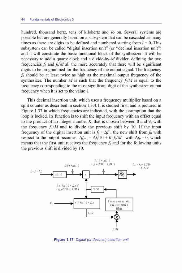
hundred, thousand hertz, tens of kilohertz and so on. Several systems are possible but are generally based on a subsystem that can be cascaded as many times as there are digits to be defined and numbered starting from i = 0. This subsystem can be called “digital insertion unit” (or “decimal insertion unit”) and it will constitute the basic functional block of the synthesizer. It will be necessary to add a quartz clock and a divide-by-M divider, defining the two frequencies f0 and f0/M all the more accurately that there will be significant digits to be programmed for the frequency of the output signal. The frequency f0 should be at least twice as high as the maximal output frequency of the synthesizer. The number M is such that the frequency f0/M is equal to the frequency corresponding to the most significant digit of the synthesizer output frequency when it is set to the value 1.
This decimal insertion unit, which uses a frequency multiplier based on a split counter as described in section 1.3.4.1, is studied first, and is pictured in Figure 1.37 in which frequencies are indicated, with the assumption that the loop is locked. Its function is to shift the input frequency with an offset equal to the product of an integer number Ki that is chosen between 0 and 9, with the frequency f0 /M and to divide the previous shift by 10. If the input frequency of the digital insertion unit is f0 + Δfi , the new shift from f0 with respect to the output becomes Δfi+1 = Δfi/10 + Ki f0/M, with Δf0 = 0, which means that the first unit receives the frequency f0 and for the following units the previous shift is divided by 10.
Figure 1.37. Digital (or decimal) insertion unit
f i = f 0 + Δ f i
f0 × (9 M /1 0 + K i) /M= f 0 × (9 /1 0 + K i/M )
f 0 /Μ
f0 /1 0 + Δ f i/1 0
V C O
- +
P h a s e c o m p a ra to ra n d c o r re c t io n
f i l te r
× 1 /1 0 ×
× 1 /(9 M /1 0 + K i)K i
f0 /M
f0 /1 0 + Δ f i/1 0 ± f0 × (9 /1 0 + K i/M ) )
f i+ 1 = f0 + Δ f i/1 0 + K i f0 /M
Discrete-time Signals and Systems 45
After cascading n+1 units, it is deduced that the output frequency is f0 + (K0 + K1/10 + K2/100 + K3/1000 + ... + Kn/10n ) f0/M which will be sent into a mixer with the frequency f0 to recover after low-pass filtering the frequency difference corresponding to all of the terms of the previous sum except the first one.
If, for example, we want to reach 999,999 Hz with a resolution of 1 Hz, by taking f0 = 10 MHz, it will be necessary that f0/M = 100 kHz, that is M = 100, and the number measuring the output frequency will consist of digits K0 K1 K2 K3 K4 K5 from left to right (K0 being the most significant, K5 being the digit of the units). In the loop of each unit, the divider based on a split counter will have to divide by 90 + Ki.
1.3.5. Digital synthesis and phase and frequency control systems
In order to design purely digital frequency synthesis systems, certain devices used in analog synthesis have to be transformed in such a manner that the flexibility is removed and limitations are imposed on a number of performances. The systems thus obtained however are much less expensive and easier to incorporate within an integrated circuit composed exclusively of logical functions. Only the direct digital synthesis of a sinusoidal signal and the digital PLL are discussed. The study of digital loops is based on the properties of the type 297 circuit from Texas Instruments [HC 297], initially built using TTL LS technology (Low Power Schottky), and then using CMOS technology, namely HC and HCT series.
1.3.5.1. Digital frequency synthesis
A simple way to generate a sinusoidal signal with predetermined frequency relies on the storage in a read-only-memory (ROM) of the digital values sin(2πi/N) of a sine wave sampled with N points for a period, numbered from i = 0 to i = N−1. It then suffices to read and transmit to an analog-to-digital converter a number n ≤ N of these values evenly spaced at the pace of a fixed sampling period Te. The period of this signal, illustrated in Figure 1.38 for n = 16, for example, will thus be nTe and it will be possible to adjust its frequency 1/(nTe) using the number n. When n = N, all samples are utilized and the frequency reaches its minimal value equal to 1/(NTe). For n < N, an integer number p should in theory still exist such that
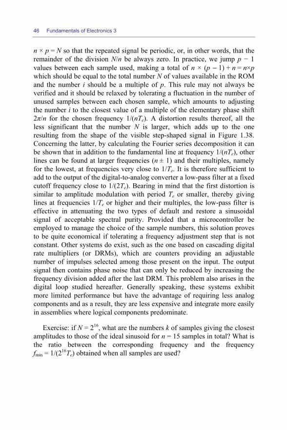
46 Fundamentals of Electronics 3
n × p = N so that the repeated signal be periodic, or, in other words, that the remainder of the division N/n be always zero. In practice, we jump p − 1 values between each sample used, making a total of n × (p − 1) + n = n×p which should be equal to the total number N of values available in the ROM and the number i should be a multiple of p. This rule may not always be verified and it should be relaxed by tolerating a fluctuation in the number of unused samples between each chosen sample, which amounts to adjusting the number i to the closest value of a multiple of the elementary phase shift 2π/n for the chosen frequency 1/(nTe). A distortion results thereof, all the less significant that the number N is larger, which adds up to the one resulting from the shape of the visible step-shaped signal in Figure 1.38. Concerning the latter, by calculating the Fourier series decomposition it can be shown that in addition to the fundamental line at frequency 1/(nTe), other lines can be found at larger frequencies (n ± 1) and their multiples, namely for the lowest, at frequencies very close to 1/Te. It is therefore sufficient to add to the output of the digital-to-analog converter a low-pass filter at a fixed cutoff frequency close to 1/(2Te). Bearing in mind that the first distortion is similar to amplitude modulation with period Te or smaller, thereby giving lines at frequencies 1/Te or higher and their multiples, the low-pass filter is effective in attenuating the two types of default and restore a sinusoidal signal of acceptable spectral purity. Provided that a microcontroller be employed to manage the choice of the sample numbers, this solution proves to be quite economical if tolerating a frequency adjustment step that is not constant. Other systems do exist, such as the one based on cascading digital rate multipliers (or DRMs), which are counters providing an adjustable number of impulses selected among those present on the input. The output signal then contains phase noise that can only be reduced by increasing the frequency division added after the last DRM. This problem also arises in the digital loop studied hereafter. Generally speaking, these systems exhibit more limited performance but have the advantage of requiring less analog components and as a result, they are less expensive and integrate more easily in assemblies where logical components predominate.
Exercise: if N = 216, what are the numbers k of samples giving the closest amplitudes to those of the ideal sinusoid for n = 15 samples in total? What is the ratio between the corresponding frequency and the frequency fmin = 1/(216Te) obtained when all samples are used?
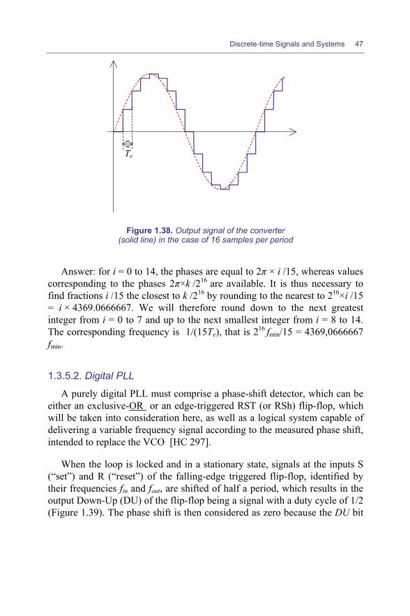
Discrete-time Signals and Systems 47
Figure 1.38. Output signal of the converter
(solid line) in the case of 16 samples per period
Answer: for i = 0 to 14, the phases are equal to 2π × i /15, whereas values corresponding to the phases 2π×k /216 are available. It is thus necessary to find fractions i /15 the closest to k /216 by rounding to the nearest to 216×i /15 = i × 4369.0666667. We will therefore round down to the next greatest integer from i = 0 to 7 and up to the next smallest integer from i = 8 to 14. The corresponding frequency is 1/(15Te), that is 216 fmin/15 = 4369,0666667 fmin.
1.3.5.2. Digital PLL
A purely digital PLL must comprise a phase-shift detector, which can be either an exclusive-OR or an edge-triggered RST (or RSh) flip-flop, which will be taken into consideration here, as well as a logical system capable of delivering a variable frequency signal according to the measured phase shift, intended to replace the VCO [HC 297].
When the loop is locked and in a stationary state, signals at the inputs S (“set”) and R (“reset”) of the falling-edge triggered flip-flop, identified by their frequencies fin and fout, are shifted of half a period, which results in the output Down-Up (DU) of the flip-flop being a signal with a duty cycle of 1/2 (Figure 1.39). The phase shift is then considered as zero because the DU bit
Te
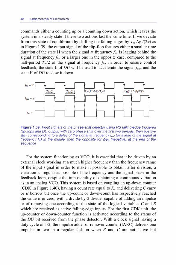
48 Fundamentals of Electronics 3
commands either a counting up or a counting down action, which leaves the system in a steady state if these two actions last the same time. If we deviate from this state of equilibrium by shifting the falling edges by Tin Δφ /(2π) as in Figure 1.39, the output signal of the flip-flop features either a smaller time duration of the state H when the signal at frequency fout is lagging behind the signal at frequency fin, or a larger one in the opposite case, compared to the half-period Tin/2 of the signal at frequency fin. In order to ensure control feedback, the state L of DU will be used to accelerate the signal fout, and the state H of DU to slow it down.
Figure 1.39. Input signals of the phase-shift detector using RS falling-edge triggered flip-flops and DU output, with zero phase shift over the first two periods, then positive Δφ1 corresponding to a delay of the signal at frequency fout (or a lead of the signal at frequency fin) in the middle, then the opposite for Δφ2 (negative) at the end of the sequence
For the system functioning as VCO, it is essential that it be driven by an external clock working at a much higher frequency than the frequency range of the input signal in order to make it possible to obtain, after division, a variation as regular as possible of the frequency and the signal phase in the feedback loop, despite the impossibility of obtaining a continuous variation as in an analog VCO. This system is based on coupling an up-down counter (CDK in Figure 1.40), having a count rate equal to K, and delivering C carry or B borrow bit once the up-count or down-count has respectively reached the value K or zero, with a divide-by-2 divider capable of adding an impulse or of removing one according to the state of the logical variables C and B which are received as active falling-edge inputs. For the first CDK unit, the up-counter or down-counter function is activated according to the status of the DU bit received from the phase detector. With a clock signal having a duty cycle of 1/2, the impulse adder or remover counter (IARC) delivers one impulse in two in a regular fashion when B and C are not active but
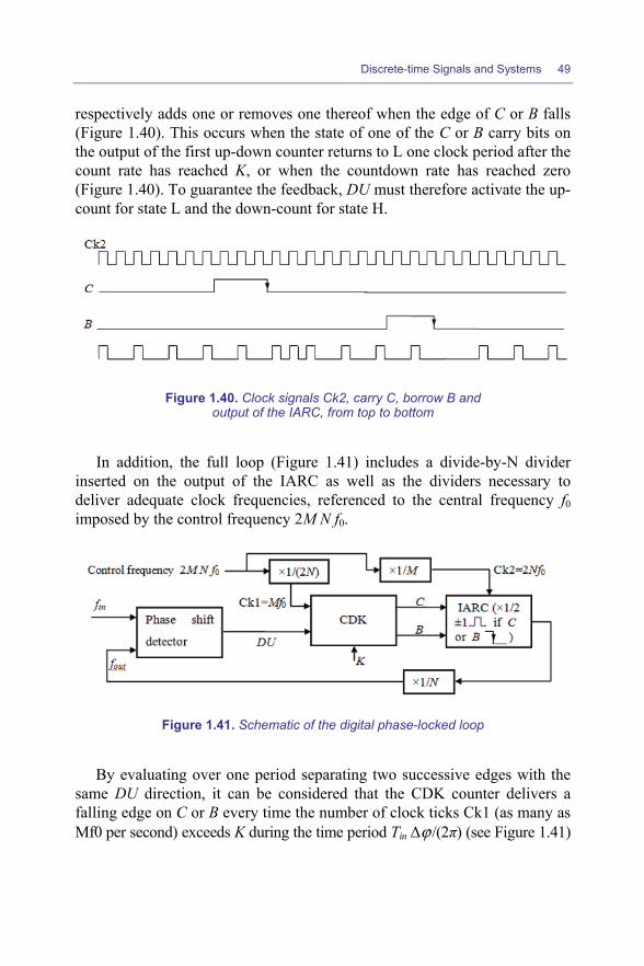
Discrete-time Signals and Systems 49
respectively adds one or removes one thereof when the edge of C or B falls (Figure 1.40). This occurs when the state of one of the C or B carry bits on the output of the first up-down counter returns to L one clock period after the count rate has reached K, or when the countdown rate has reached zero (Figure 1.40). To guarantee the feedback, DU must therefore activate the up-count for state L and the down-count for state H.
Figure 1.40. Clock signals Ck2, carry C, borrow B and output of the IARC, from top to bottom
In addition, the full loop (Figure 1.41) includes a divide-by-N divider inserted on the output of the IARC as well as the dividers necessary to deliver adequate clock frequencies, referenced to the central frequency f0 imposed by the control frequency 2M N f0.
Figure 1.41. Schematic of the digital phase-locked loop
By evaluating over one period separating two successive edges with the same DU direction, it can be considered that the CDK counter delivers a falling edge on C or B every time the number of clock ticks Ck1 (as many as Mf0 per second) exceeds K during the time period Tin Δϕ /(2π) (see Figure 1.41)
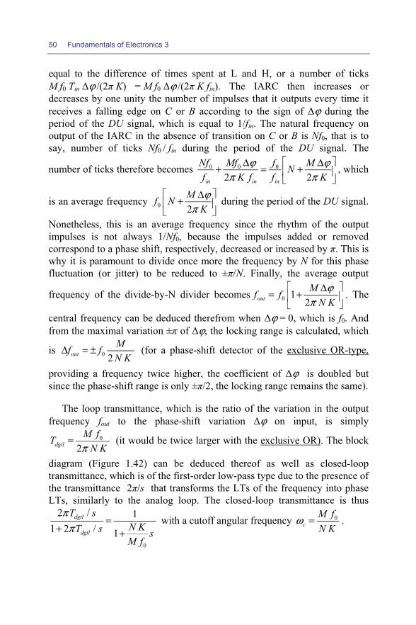
50 Fundamentals of Electronics 3
equal to the difference of times spent at L and H, or a number of ticks M f0 Tin Δϕ /(2π K) = M f0 Δϕ /(2π K fin). The IARC then increases or decreases by one unity the number of impulses that it outputs every time it receives a falling edge on C or B according to the sign of Δϕ during the period of the DU signal, which is equal to 1/fin. The natural frequency on output of the IARC in the absence of transition on C or B is Nf0, that is to say, number of ticks Nf0 / fin during the period of the DU signal. The
number of ticks therefore becomes 0 0 0
2 2in in in
Nf Mf f MNf K f f K
ϕ ϕπ π
Δ Δ+ = +
, which
is an average frequency 0 2Mf N
Kϕ
π Δ+
during the period of the DU signal.
Nonetheless, this is an average frequency since the rhythm of the output impulses is not always 1/Nf0, because the impulses added or removed correspond to a phase shift, respectively, decreased or increased by π. This is why it is paramount to divide once more the frequency by N for this phase fluctuation (or jitter) to be reduced to ±π/N. Finally, the average output
frequency of the divide-by-N divider becomes 0 12outMf f
N Kϕ
π Δ= +
. The
central frequency can be deduced therefrom when Δϕ = 0, which is f0. And from the maximal variation ±π of Δϕ, the locking range is calculated, which
is 0 2outMf fN K
Δ = ± (for a phase-shift detector of the exclusive OR-type,
providing a frequency twice higher, the coefficient of Δϕ is doubled but since the phase-shift range is only ±π/2, the locking range remains the same).
The loop transmittance, which is the ratio of the variation in the output frequency fout to the phase-shift variation Δϕ on input, is simply
0
2dgtlM fT
N Kπ= (it would be twice larger with the exclusive OR). The block
diagram (Figure 1.42) can be deduced thereof as well as closed-loop transmittance, which is of the first-order low-pass type due to the presence of the transmittance 2π/s that transforms the LTs of the frequency into phase LTs, similarly to the analog loop. The closed-loop transmittance is thus
0
2 / 11 2 / 1
dgtl
dgtl
T sN KT s sM f
ππ
=+ +
with a cutoff angular frequency 0c
M fN K
ω = .

Discrete-time Signals and Systems 51
Choice of parameters and phase noise reduction
The division rates M, N and K are determined based on criteria
concerning the cutoff frequency KNfM
c0=ω , the locking
range 0 12outMf f
N Kϕ
π Δ= +
, whereas the central frequency of the locking
range is set by f0. The phase noise is characterized by a phase jitter ±π/N. It is necessary that M /K must be kept well below N to ensure a pace of the edges on C and B slower than Ck2 to decrease the phase jitter. In order to go further, N must be taken as large enough, which requires M to be set to an even larger value.
Figure 1.42. Block diagram of the digital PLL
Figure 1.43. Digital PLL with phase noise reduction
Nevertheless, it is possible to remove this phase noise in steady state when the loop is locked with fout = fin, close to f0. In effect, if the number of clock ticks Ck1 is enough for half a period of the DU signal, that is to say also half a period of input and output signals 1/(2fout), the up-counts or down-counts achieved by the CDK counter will overflow the values K or 0, thus

52 Fundamentals of Electronics 3
generating addition and removal of impulses by the IARC for each period of the output signal. The two effects will cancel each other at the level of the average frequency but lead to unnecessary phase fluctuations that can possibly be removed by adjusting the count rates in such a way that these overflows do not occur, that is to say M f0 /(2f0) < K, or K > M/2.
However, a more radical solution involves activating the CDK counter only when strictly necessary, namely when Δϕ ≠ 0. To do this, we utilize a validation input “En” (“Enable”) of this counter that requires it to remain at rest, while Δϕ = 0. Provided that we have a duty cycle of 1/2 for signal fin and that N is chosen as being even, which causes that the duty cycle of the signal fout is also 1/2, this signal can be generated by carrying out the exclusive OR of the complement of the DU signal with the output signal fout, which yields the diagram in Figure 1.43 with an RS flip-flop as phase-shift detector. In this way, C or B signals are generated only when necessary, namely when Δϕ ≠ 0, which confines the phase noise to the case in which the loop is not locked. This technique is also possible with the exclusive OR-based detector using a slightly different circuitry. On the other hand, it should be highlighted that phase noise remains if the loop is employed, for example, to demodulate a phase or frequency modulated signal. The only way to reduce it in this case is therefore to increase N, but this leads to an increase in clock frequencies which can limit f0 to a few megahertz if the HC297-based commercial circuit, limited to a few tens of megahertz for these clock frequencies, is employed. This technique also has the disadvantage of slowing down transient states by reducing ωc. To allow for higher frequencies, the same functions have to be implemented in a much faster integrated logical technology.
Applications of this type of digital loop fall under the scope of the field of the demodulation of digital phase or frequency-modulated signals (phase-shift keying or PSK, frequency-shift keying or FSK) and that of the recovery of carriers, useful, for example, for read accesses in hard drives. Complementary circuits enabling locking detection, the extension of the locking range by splitting the divide-by-N divider in two, the use of the parallel outputs of the divide-by-N divider, parameter control using microprocessors and so forth, can be added in order to increase the versatility of the loop and to adapt it to the requirements of the intended application.
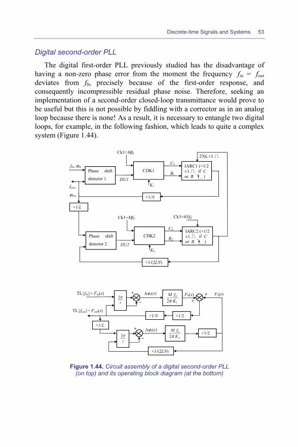
Discrete-time Signals and Systems 53
Digital second-order PLL
The digital first-order PLL previously studied has the disadvantage of having a non-zero phase error from the moment the frequency fin = fout deviates from f0, precisely because of the first-order response, and consequently incompressible residual phase noise. Therefore, seeking an implementation of a second-order closed-loop transmittance would prove to be useful but this is not possible by fiddling with a corrector as in an analog loop because there is none! As a result, it is necessary to entangle two digital loops, for example, in the following fashion, which leads to quite a complex system (Figure 1.44).
Phase shift
detector 1
fin, ϕin CDK1
DU1
Ck1=Mf0
K1
IARC1 (×1/2 ±1 if C or B )
×1/N
C1
B1
fout,
ϕout
2Nf0 ±1
Phase shift
detector 2
CDK2
DU2
Ck1=Mf0
K2
IARC2 (×1/2 ±1 if C or B )
×1/(2LN)
Ck3=4Nf0
×1/L
C2
B2
2sπ
TL{fout}= Fout(s)
−
+
1
0
2 KfM
πΔϕ1(s) +
+
×1/2×1/N
2sπ −
+
2
0
2 KfM
π
×1/(2LN)
×1/L
×1/2
TL{fin}= Fin(s)
Δϕ2(s)
F4(s) F5(s)
Figure 1.44. Circuit assembly of a digital second-order PLL
(on top) and its operating block diagram (at the bottom)
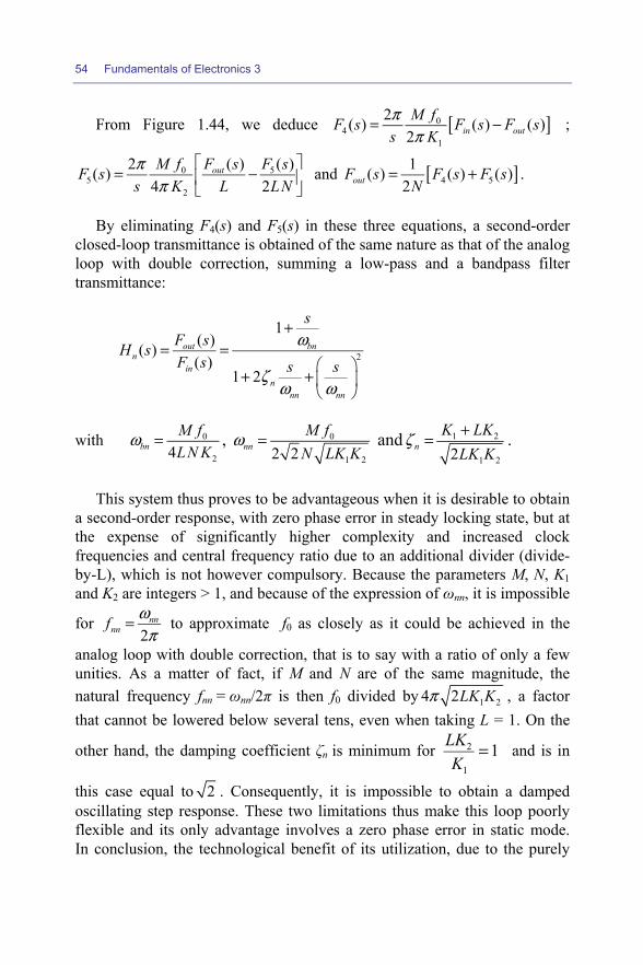
54 Fundamentals of Electronics 3
From Figure 1.44, we deduce [ ]04
1
2( ) ( ) ( )2 in outM fF s F s F s
s Kπ
π= − ;
0 55
2
2 ( ) ( )( )4 2
outM f F s F sF ss K L LNπ
π
= −
and [ ]4 51( ) ( ) ( )
2outF s F s F sN
= + .
By eliminating F4(s) and F5(s) in these three equations, a second-order closed-loop transmittance is obtained of the same nature as that of the analog loop with double correction, summing a low-pass and a bandpass filter transmittance:
2
1( )( )( )
1 2
out bnn
inn
nn nn
sF sH sF s s s
ω
ζω ω
+= =
+ +
with 0
24bnM fLN K
ω = , 0
1 22 2nnM fN LK K
ω = and 1 2
1 22nK LK
LK Kζ += .
This system thus proves to be advantageous when it is desirable to obtain
a second-order response, with zero phase error in steady locking state, but at the expense of significantly higher complexity and increased clock frequencies and central frequency ratio due to an additional divider (divide-by-L), which is not however compulsory. Because the parameters M, N, K1 and K2 are integers > 1, and because of the expression of ωnn, it is impossible
for 2
nnnnf ω
π= to approximate f0 as closely as it could be achieved in the
analog loop with double correction, that is to say with a ratio of only a few unities. As a matter of fact, if M and N are of the same magnitude, the natural frequency fnn = ωnn/2π is then f0 divided by 1 24 2LK Kπ , a factor that cannot be lowered below several tens, even when taking L = 1. On the
other hand, the damping coefficient ζn is minimum for 11
2 =K
LK and is in
this case equal to 2 . Consequently, it is impossible to obtain a damped oscillating step response. These two limitations thus make this loop poorly flexible and its only advantage involves a zero phase error in static mode. In conclusion, the technological benefit of its utilization, due to the purely

Discrete-time Signals and Systems 55
digital nature of the circuits employed and the possibility of controlling its parameters with a microcontroller, must be compared to the inherent drawbacks, to the limitations in terms of frequency and to those imposed on the parameters of the control.
1.4. Sampled systems
1.4.1. Z-transform for systems described by a recurrence equation (or difference equation)
We shift from the LT of the response y(t) of a continuous-time system to that of the corresponding sampled system by applying the “Dirac comb” distribution with time period Te on y(t) exp(−st):
0 00
( ) ( ) ( )exp( ) ( )exp( ) [ ] .ke e e
k k kY z t kT y t st dt y kT skT y k zδ
∞ ∞ ∞ ∞−
=−∞ = =
= − − = − =
The z-transform (ZT) is thus defined by establishing z = exp(sTe) and z−1 = exp(−sTe) corresponding to the delay operator of one sampling period. Denoting the samples by y[k] to shorten the notation y(kTe) and to use the kth-order number of the sequence, we can write:
{ }0
( ) [ ] .k
kZT y t y k z
∞−
=
=
The ZT of a recurrence equation or difference equation exhibiting a linear combination of the different samples y[i], y[i−1], y[i−2], and so on, is thus easily obtained by multiplying the value of each sample by z−i, z−i+1, z−i+2 and so on, according to the delay of the sample with regard to the time origin, measured in the sampling period unit Te. The variable z being dimensionless, the ZT retains the dimension of the function y(t).
The resulting series is convergent provided that |z| > L, in which L is a
convergence radius. From the identity 1
0
11
nni
i
uuu
+
=
−=− , it is deduced that the

56 Fundamentals of Electronics 3
geometric series ( ) ( )( )
1
10
1
1
nni
i
azaz
az
− −−
−=
−=
−∑ converges to
( ) 1
11 az −−
when
n → ∞ only if |az| > 1, that is if 1za
> , hence L = a. We can then
calculate the transform of all ordinary functions with the Heaviside step function U(t) in factors to ensure the causal nature, which allows us to create the dictionary of transforms hereafter (Table 1.1).
y(t) y[k] Y(z) = ZT{y(t)}
δ(t) y[0] = 1/Te * and y[k] = 0 for k ≠ 0 1/Te *
δ(t − kTe) y[k] = 1/Te * and y[k'] = 0 for k' ≠ k
* see below and note in section 7.4.2
z−k/Te *
* see below and note in section 7.4.2
U(t) y[k] = 1 ∀ k ≥ 0 111
−−z
t U(t) y[k] = k ∀ k ≥ 0 ( )21
1
1 −
−
− zz
exp(−αt) U(t)
with α > 0 y[k] = exp(−αkTe) ∀ k ≥ 0 11
1−−− ze eTα
exp(−σ t)cos(ω0t)U(t)
with σ > 0
y[k] = exp(−σkTe) cos(ω0kTe ) ∀ k ≥0 22
01
01
)cos(21)cos(1
−−−−
−−
+−−
zeTzeTze
ee
e
Te
Te
T
σσ
σ
ωω
exp(−σ t) sin(ω0t)U(t)
with σ > 0
y[k] = exp(−σkTe) sin(ω0kTe )
∀ k ≥0 22
01
01
)cos(21)sin(
−−−−
−−
+− zeTzeTze
ee
e
Te
Te
T
σσ
σ
ωω
exp(−σ t)cos(ω0t+ϕ 0)U(t)
with σ > 0
y[k] = exp(−σkTe) cos(ω0kTe +ϕ 0)
∀ k ≥0 22
01
001
0
)cos(21)cos()cos(
−−−−
−−
+−−−
zeTzeTze
ee
e
Te
Te
T
σσ
σ
ωϕωϕ
exp(−σ t) sin(ω0t+ϕ 0)U(t)
with σ > 0 y[k] = exp(−σkTe) sin(ω0kTe +ϕ 0)
∀ k ≥0 22
01
001
0
)cos(21)sin()sin(
−−−−
−−
+−−+
zeTzeTze
ee
e
Te
Te
T
σσ
σ
ωϕωϕ
Table 1.1. Continuous-time, sampled signals and their z-transforms
However, the ZT, such as that presented above, cannot be applied to distributions such as the Dirac impulse δ(t), as the “Dirac comb” distribution is already present in the definition, the signal would therefore be sampled twice. Such an operation would not make sense and it is thus necessary to substitute δ(t) with an ordinary function homogeneous to the reciprocal of
Discrete-time Signals and Systems 57
time and that possesses an area under the curve equal to 1, in order to fulfill the properties of δ(t). By convention and because there is only a single sample per sampling period, a time step of duration Te and amplitude 1/Te is chosen, which ensures the consistency of the computations of the ZT of the impulse response of continuous-time systems with those of already sampled systems.
Properties of the ZT defined by { }0
( ) [ ] k
kZT y t y k z
∞−
=
=
– Lag (with x[k] causal) : if y[k] = x[k− k’] (with k’ > 0), Y(z) = z−k’ X(z)
– Lead: if y[k] = x[k + k’] (with k’ > 0), Y(z) = ' 1
'
0( ) [ ]
kk k
kz X z x k z
−−
=
−
– Time summation, integration, interpolation: by applying the definition
to 0
[ ] [ ]k
iy k x i
=
= , it is shown that 11( ) ( )
1Y z X z
z−=−
. As a matter of fact:
{ } ( )
0 0 0 0 0TZ ( ) [ ] [ ] [ ]
k kk k i k i
k k i k iy t y k z x i z x i z z
∞ ∞ ∞− − − − −
= = = = =
= = =
1 2
0 1 2[0] ( [0] [1]) ( [0] [1] [2]) [0] [1] [2]k k k
k k kx x x z x x x z x z x z x z
∞ ∞ ∞− − − − −
= = =
= + + + + + + = + + +
( )1 2 1 21
0 0 0 0
( )[0] [1] [2] [0] [1] [2]1
k k k k
k k k k
X zx z x z z x z z x x z x z zz
∞ ∞ ∞ ∞− − − − − − − −
−= = = =
= + + + = + + + =− .
For a pure integrator (of transmittance 1/s obtained by LT in the continuous-time domain), we can calculate an approximation to the integral of the samples using the right rectangle method, and by recurrence: y[k] = y[k−1] + Te x[k]. The ZT provides the corresponding transmittance
11)()(
−−=
zT
zXzY e . If rather x[k−1] is chosen (left rectangle method), we obtain
1
1
1)()(
−
−
−=
zzT
zXzY e , whereas the trapeze method makes use of the interpolation
y[k] = y[k−1] + Te (x[k]+ x[k−1])/2, whose ZT is: ( )( )1
1
121
)()(
−
−
−+=
zzT
zXzY e .
Concerning the same integrators which directly manage the samples in the discrete-time domain, the same ZT is obtained but devoid of factor Te. They are often represented by an operation diagram incorporating a delay of one
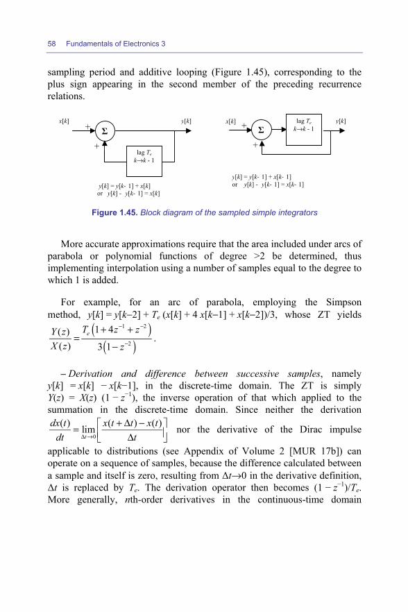
58 Fundamentals of Electronics 3
sampling period and additive looping (Figure 1.45), corresponding to the plus sign appearing in the second member of the preceding recurrence relations.
Figure 1.45. Block diagram of the sampled simple integrators
More accurate approximations require that the area included under arcs of parabola or polynomial functions of degree >2 be determined, thus implementing interpolation using a number of samples equal to the degree to which 1 is added.
For example, for an arc of parabola, employing the Simpson method, y[k] = y[k−2] + Te (x[k] + 4 x[k−1] + x[k−2])/3, whose ZT yields
( )( )
1 2
2
1 4( )( ) 3 1
eT z zY zX z z
− −
−
+ +=
−.
– Derivation and difference between successive samples, namely y[k] = x[k] − x[k−1], in the discrete-time domain. The ZT is simply Y(z) = X(z) (1 − z−1), the inverse operation of that which applied to the summation in the discrete-time domain. Since neither the derivation
0
( ) ( ) ( )limt
dx t x t t x tdt tΔ →
+ Δ − = Δ nor the derivative of the Dirac impulse
applicable to distributions (see Appendix of Volume 2 [MUR 17b]) can operate on a sequence of samples, because the difference calculated between a sample and itself is zero, resulting from Δt→0 in the derivative definition, Δt is replaced by Te. The derivation operator then becomes (1 − z−1)/Te. More generally, nth-order derivatives in the continuous-time domain
+
y[k] = y[k- 1] + x[k]or y[k] - y[k- 1] = x[k]
y[k] = y[k- 1] + x[k- 1]or y[k] - y[k- 1] = x[k- 1]
y[k]x[k]Σ
+
+ lag Tek→k - 1Σ+
lag Tek→k - 1
y[k]x[k]

Discrete-time Signals and Systems 59
are replaced by the differences [ ] [ ]n
e
x k x k nT
− − in the discrete-time domain,
whose ZT are ( ) ( )n
ne
X z z X zT
−− .
– Derivation in the complex z-plane of the ZT: by deriving z−k we obtain −k z−k− 1 from which
{ }( ) 1 '
0 ' 0
( )( ) ( ) [ ] [ ']k k
k k
d TZ x tdX z Y z k x k z y k zdz dz
∞ ∞− − −
= =
= = = − = which cor-
responds by identifying the coefficients of the powers of z to k’ = k+1, and to y[k+1] = −k x[k].
– Poles: for the first-order transmittance (Table 1.1), the denominator cancels for z = z1 = exp(−αTe), corresponding to a real pole −α in the plane of the s variable. The roots of the denominator of the last four second-order expressions of the previous table multiplied by 2 2eTe zσ in order to obtain the poles directly in the z-plane are 0e eT j Tz e eσ ω− ±
± = , which are complex conjugates and correspond to the poles −σ ± jω0 in the plane of the s variable. In these denominators, we recognize the opposite of the sum of poles as the coefficient of z−1 and the product of the poles in the z-plane as the coefficient of z−2.
– Transmittance stability criterion in rational fractions F(z): it follows from the Nyquist criterion that indicates that there should be no poles of F(s) in the right half-plane of the complex plane of the s variable, limited by s = jω, when ω is going from −∞ to +∞. Applying the transformation z = exp(jωTe), the image of z in the complex plane of the z variable follows a circle of radius 1 when ω goes from −π fe to +π fe , then repeatedly beyond this interval. The poles pi = σi ± jωi with positive real part σi give poles zi = exp(σi Te) exp(±jωi Te) in the z-plane, and their images are located outside the circle of radius 1, which cause instability of the system. It should be noted that on the contrary pi = −σs ± jωs with σs > 0 involves poles with negative real parts in the plane of the s variable, characteristic of a stable system and gives poles inside the circle of radius 1 in the z-plane:
A system is stable if its rational transmittance F(z) has only poles inside the circle of radius 1 in the complex plane of the z variable.

60 Fundamentals of Electronics 3
The elementary first-order transmittance 1
11 eTe zα− −−
is thus stable if
α > 0, and since the modulus of the poles of the second-order elementary transmittances is s eTe σ− , these transmittances are equally stable with σs > 0, which corresponds to a damped time response either converging towards 0 or towards a constant, that is also non-divergent.
– Initial and final values: when z → +∞, all terms having non-zero powers of z−1 cancel out for a convergent series Y[z] and therefore only the first term remains, that is:
( ) [0]limz
Y z y→+∞
= , initial value of the time series.
According to the lead theorem: TZ{y(t+Te) − y(t) } = z (Y(z) − y[0]) − Y(z)
but also TZ{y(t+Te) − y(t) } = ( )0
[ 1] [ ] k
ky k y k z
∞−
=
+ − which tends to
y[∞] − y[0] when z →1, which delivers the final value of the series: 1
1 1[ ] ( 1) ( ) (1 ) ( )lim lim lim
k z zy k z Y z z Y z−
→+∞ → →= − = − from the comparison of both results.
– Inverse transform: if we limit ourselves to the values of the original function evaluated only at the sampling times, two techniques can be employed, the second being particularly direct:
- Partial fraction decomposition of the rational function and identification with items found in the dictionary of ZTs (Table 1.1).
- Division of the numerator by the denominator according to the increasing powers of z−1 from 0, that is to say according to the increasingly negative powers of z. According to the definition of ZT, the sample sequence then simply consists of the coefficients of z0, z−1, z−2, z−3, … z−k.

Discrete-time Signals and Systems 61
1.4.2. Continuous-time systems subject to a sampled signal
For a causal continuous-time system whose impulse response is h(t), the response y(t) to an input x(t) is given by the convolution product (Chapter 2
of Volume 2 [MUR 17b]) 0
( ) ( ) ( )y t h x t dτ τ τ∞
= − . If definition
0
( ) ( ) ( )exp( )ek
Y z t kT y t pt dtδ∞ ∞
=−∞
= − − is applied to this convolution product
in order to determine the ZT of the sampled response, it still follows that
0( ) [ ] k
kY z y k z
∞−
=
= .
This expression depends on the discrete samples y[k], which are therefore to be determined. In the same way that linearity and stationarity properties allow us to calculate the output of a continuous-time system by the convolution of the input signal and the impulse response (see Chapter 2 of Volume 2 [MUR 17b]), they can be defined by the discrete convolution:
0 0[ ] [ ] [ ] [ ] [ ]
i iy k x i h k i h i x k i
∞ ∞
= =
= − = − . Then TZ{y(t)} =
( ) ( )
0 0 0 0 0 0[ ] [ ] [ ] [ ] [ ] [ ]k i k i i k i
k i k i i kx i h k i z x i z h k i z x i z h k i z
∞ ∞ ∞ ∞ ∞ ∞− − − − − − −
= = = = = =
− = − = −
0 0
[ ] [ ] ( ) ( )i k
i kx i z h k z X z Y z
∞ ∞− −
= =
= = because the samples h[k−i] are 0 for
k < i for a causal system.
Conclusion: the product of the z-transmittance of either a continuous or sampled system by the ZT of the input signal thus provides the ZT of the output signal.
The z-transmittance of any transfer function involving any physical quantity can thus be determined. In the case where the corresponding impulse response h(t) is available, we apply the definition of the ZT given at the beginning of section 1.4.1.

62 Fundamentals of Electronics 3
When we know the Laplace transmittance T(s) = TL{h(t)}, the simplest method is to return to the corresponding impulse response (see tables of Chapters 1 and 2, Volume 2 [MUR 17b]) and to sample it, or more precisely to calculate h(kTe), which is normalized by the period Te, to obtain h[k] then
∑∞
=
−
0][
k
kzkh . In effect, the convolution in the continuous-time domain is an
integral whose result must be expressed with the same units as the input signal when the system does not change the dimension of the input quantity, which requires that h(t) be inverse time-homogeneous in this case. Nonetheless, this no longer holds with the discrete convolution and h[k] should be calculated as an integral of h(t) over the period Te. In fact, we will always use the rectangle approximation by simply carrying out the product of h(kTe) by Te. This is consistent with the respective dimensions of δ(t) (inverse-time) and U(t) (dimensionless) that appear in h(t). The case of analog filters is treated in the following table based on the impulse responses given in Chapter 2 of Volume 2 [MUR 17b] and the ZT dictionary of section 1.4.1.
H(s) Impulse response h(kTe) H(z)
c
csωω+
(first order low-pass) ωc U(t) exp(−ωc kTe)
11 −−− zeT
ecTec
ωω
c
ss ω+
(first order high-pass) δ(t) − ωc U(t) exp(−ωc kTe) 1
1
11
−−
−−
−−−
zezeT
ec
ec
T
Tec
ω
ωω
2
2 22n
n ns sω
ζω ω+ +
(second order low-
pass)
[ ]enenn kTkTt 2
2−1
−1
)− ζωζζωω
sinexp(
)(U [ ][ ] 221
1
cos21
sin
−−−2−
−2−
2
+−1−
−1⎟⎟
⎠
⎞
⎜⎜
⎝
⎛
−1
zezTe
zTeT
enen
en
Ten
T
enTen
ζωζω
ζω
ζω
ζωζ
ω
2 22n
n n
ss s
ω
ζω ω+ +
(second order
band-pass)
[ ]0cosexp(
)( ϕζωζζωω
+−1−1
)− 2
2 enenn kTkTtU
with sin(ϕ0)=ζ
[ ][ ] 221
01
0
cos21
)cos()cos(
−−−2−
2−−
2
+−1−
−−1−⎟⎟
⎠
⎞
⎜⎜
⎝
⎛
−1
zezTe
TezT
enen
en
Ten
T
enTen
ζωζω
ζω
ζω
ϕζωϕζ
ω
2
2 22 n n
ss sζω ω+ +
(second order
high-pass)
−)(tδ
[ ]02sinexp()( ϕζωζζωω +−1
−1)− 2
2 enenn kTkTtU
[ ][ ] 221
01
0
cos21
)2sin()2sin(
1
−−−2−
2−−
2
+−1−
−−1+⎟⎟
⎠
⎞
⎜⎜
⎝
⎛
−1
−
zezTe
TezT
enen
en
Ten
T
enTen
ζωζω
ζω
ζω
ϕζωϕζ
ω
Table 1.2. Impulse response and z-transform of elementary analog filters

Discrete-time Signals and Systems 63
1.4.3. Switched-capacitor circuits and infinite impulse response (IIR) filters
1.4.3.1. Analysis of the effects of switching on the charges stored in capacitors and the passive first order low-pass filter
MOS switches associated with capacitors and eventually operational amplifiers provide means to build all types of z-transmittance. Type P and I switches (MOS transistors) are respectively switched off during the half sampling period when the control is 0 and switched on (closed contact) when it is 1. P is in phase with integer times and I in inverse phase, that is, switched on in synchronization with half-integer times (see Figure 1.46). There is no overlap of closures over time (“break-before-make switch”) and charge transfers are supposed to be immediate because the resistances of the switch are neglected.
Example of the passive low-pass filter:
P
S E
C2 = C
I
Q2 i2
P
I
k − 1 k − 1/2 k k + 1/2 t / Te
1
0
1
0
C1 = aC
Q1 i1
Figure 1.46. Switch status (0 = switched off or open; 1 = switched on
or closed) and circuit of the low-pass filter
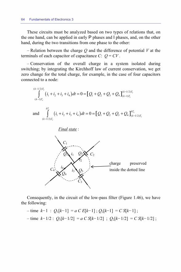
64 Fundamentals of Electronics 3
These circuits must be analyzed based on two types of relations that, on the one hand, can be applied in early P phases and I phases, and, on the other hand, during the two transitions from one phase to the other:
– Relation between the charge Q and the difference of potential V at the terminals of each capacitor of capacitance C: Q = CV .
– Conservation of the overall charge in a system isolated during switching; by integrating the Kirchhoff law of current conservation, we get zero change for the total charge, for example, in the case of four capacitors connected to a node:
( ) [ ]( 1/2)
( 1/2)1 2 3 4 1 2 3 4 ( 1)
( 1)
0e
e
e
e
k Tk Tk T
k T
i i i i dt Q Q Q Q−
−
−−
+ + + = = + + +
and ( ) [ ]1 2 3 4 1 2 3 4 ( 1/2)( 1/2)
0e
e
e
e
kTkTk T
k T
i i i i dt Q Q Q Q −−
+ + + = = + + +
Final state :
C2 Q2
i2
C1
Q1 i1
i4
Q4 C4
C3
i3 Q3 charge preserved inside the dotted line
Consequently, in the circuit of the low-pass filter (Figure 1.46), we have the following:
– time k−1 : Q1[k−1] = a C E[k−1] ; Q2[k−1] = C S[k−1] ;
– time k−1/2 : Q1[k−1/2] = a C S[k−1/2] ; Q2[k−1/2] = C S[k−1/2] ;
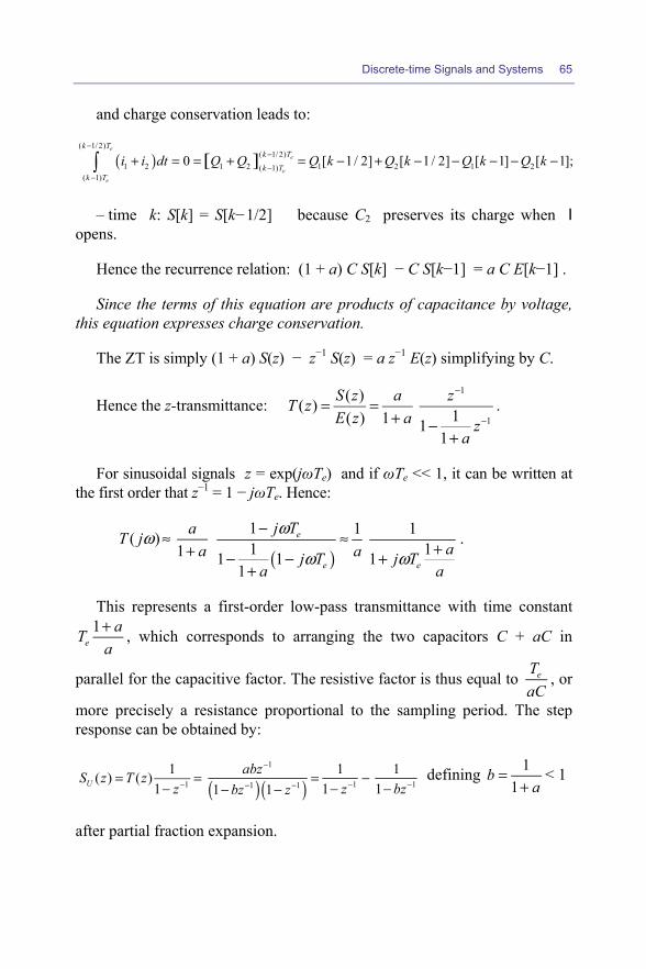
Discrete-time Signals and Systems 65
and charge conservation leads to:
( ) [ ]( 1/ 2)
( 1/ 2)1 2 1 2 1 2 1 2( 1)
( 1)
0 [ 1 / 2] [ 1 / 2] [ 1] [ 1];e
e
ee
k Tk T
k Tk T
i i dt Q Q Q k Q k Q k Q k−
−
−−
+ = = + = − + − − − − −
– time k: S[k] = S[k−1/2] because C2 preserves its charge when I opens.
Hence the recurrence relation: (1 + a) C S[k] − C S[k−1] = a C E[k−1] .
Since the terms of this equation are products of capacitance by voltage, this equation expresses charge conservation.
The ZT is simply (1 + a) S(z) − z−1 S(z) = a z−1 E(z) simplifying by C.
Hence the z-transmittance: 1
1
( )( ) 1( ) 1 11
S z a zT zE z a z
a
−
−= =
+ −+
.
For sinusoidal signals z = exp(jωTe) and if ωTe << 1, it can be written at the first order that z−1 = 1 − jωTe. Hence:
( )1
aT ja
ω ≈+
( )
1 1 11 11 1 1
1
e
e e
j Taaj T j T
a a
ω
ω ω
− ≈ +− − ++
.
This represents a first-order low-pass transmittance with time constant 1
eaT
a+ , which corresponds to arranging the two capacitors C + aC in
parallel for the capacitive factor. The resistive factor is thus equal to eTaC
, or
more precisely a resistance proportional to the sampling period. The step response can be obtained by:
( )( )1
1 1 11 1
1 1 1( ) ( ) 1 1 11 1U
abzS z T zz z bzbz z
−
− − −− −= = = −
− − −− −defining 1
1b
a=
+< 1
after partial fraction expansion.

66 Fundamentals of Electronics 3
The first term corresponds to the ZT of the Heaviside step function and the second term to the ZT of successive samples of amplitude bk according to the table of transforms. It is also possible to find this result by carrying out the division of the numerator by the denominator expanded from the fraction
not decomposed, that is ( )1
( ) 1 k kU
kS z b z
∞−
=
= − .
The amplitudes of the samples sU[k] = 1−bk are the coefficients of z0, z−1, z−2, z−3, … z−k:
k
sU[k] = 1 − bk
0
1
Figure 1.47. Step response of the first-order low-pass filter
The straight line passing through the first two samples (Figure 1.47), equivalent to the tangent at the origin in the continuous-time domain, cuts the ordinate 1 in k ≈ a
ab
+=−1
11 , which again correctly yields a time
constant 1e
aTa+ if we make the analogy with the response of the
continuous-time first-order low-pass circuit.
1.4.3.2. Assembly using operational amplifiers and charge transfer transmittances; basic IIR (infinite impulse response) filters
The use of an operational amplifier (or several) and negative feedback magnifies the possibilities. The basic circuit for obtaining the first-order transmittance, of the first degree in z in the numerator and in the denominator, can be found in Figure 1.48.
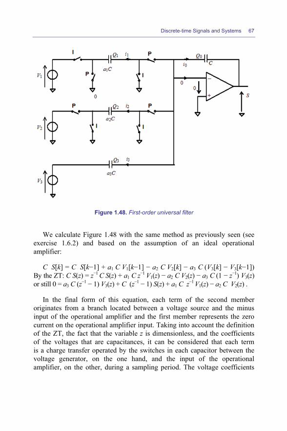
Discrete-time Signals and Systems 67
Figure 1.48. First-order universal filter
We calculate Figure 1.48 with the same method as previously seen (see exercise 1.6.2) and based on the assumption of an ideal operational amplifier:
C S[k] = C S[k−1] + a1 C V1[k−1] − a2 C V2[k] − a3 C (V3[k] − V3[k−1]) By the ZT: C S(z) = z−1 C S(z) + a1 C z−1 V1(z) − a2 C V2(z) − a3 C (1 − z−1) V3(z) or still 0 = a3 C (z−1 − 1) V3(z) + C (z−1 − 1) S(z) + a1 C z−1 V1(z) − a2 C V2(z) .
In the final form of this equation, each term of the second member originates from a branch located between a voltage source and the minus input of the operational amplifier and the first member represents the zero current on the operational amplifier input. Taking into account the definition of the ZT, the fact that the variable z is dimensionless, and the coefficients of the voltages that are capacitances, it can be considered that each term is a charge transfer operated by the switches in each capacitor between the voltage generator, on the one hand, and the input of the operational amplifier, on the other, during a sampling period. The voltage coefficients
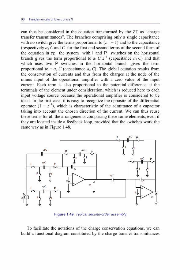
68 Fundamentals of Electronics 3
can thus be considered in the equation transformed by the ZT as “charge transfer transmittances”. The branches comprising only a single capacitance with no switch give the terms proportional to (z−1 − 1) and to the capacitance (respectively a3 C and C for the first and second terms of the second form of the equation in z); the system with I and P switches on the horizontal branch gives the term proportional to a1 C z−1 (capacitance a1 C) and that which uses two P switches in the horizontal branch gives the term proportional to − a2 C (capacitance a2 C). The global equation results from the conservation of currents and thus from the charges at the node of the minus input of the operational amplifier with a zero value of the input current. Each term is also proportional to the potential difference at the terminals of the element under consideration, which is reduced here to each input voltage source because the operational amplifier is considered to be ideal. In the first case, it is easy to recognize the opposite of the differential operator (1 − z−1), which is characteristic of the admittance of a capacitor taking into account the chosen direction of the current. We can thus reuse these terms for all the arrangements comprising these same elements, even if they are located inside a feedback loop, provided that the switches work the same way as in Figure 1.48.
Figure 1.49. Typical second-order assembly
To facilitate the notations of the charge conservation equations, we can build a functional diagram constituted by the charge transfer transmittances
Discrete-time Signals and Systems 69
from all branches and the adders imposing that currents and voltage be equal to 0 on the input of operational amplifiers (see section 1.5 and exercise 1.6.2).
By adding a second assembly based on operational amplifiers and by re-looping on the minus input of the first operational amplifier, we obtain the second-order transmittance, of the second degree in z in the numerator and in the denominator (Figure 1.49 and exercise 1.6.2).
The basic second-order filter thus constructed has a transfer function in z that is written in the following general way:
1 21 2 3
1 21 2 3
( )( )( )( )( )
i i i ni nii
i i i di di
b b z b z z z z zH zd d z d z z z z z
− −
− −
+ + − −= =
+ + − −.
Provided that a branch is introduced and located between the source connected to the input and the second operational amplifier (a2C), as in Figure 1.49, we can choose the relative sign of the coefficients of the numerator and denominator of this transmittance in z (see exercise 1.6.2). By cascading these arrangements, it thus becomes possible to obtain second-, fourth-, sixth-order-; and so on, transmittances with easily computable poles. It is also possible to use a multiple feedback loop-based assembly and to build ladder filters in which each cell, most often of the second order, is equivalent to one among those studied in Chapter 2 of Volume 2 [MUR 17b] for image-matching filters. These cells can incorporate, on the one hand, capacitor admittances proportional to the differential operator (z−1 − 1) apart from the sign as previously reported, and, on the other hand, inductance admittances proportional to the integration operator (z-1 − 1)−1 that have to be developed with an operational amplifier. Strategies that take into account and fix most imperfections of this type of active component and CMOS switch must be implemented (refer to [BAI 96], because a more detailed study of these systems will not be discussed here). We can thus produce ladder filters between two terminations when the solution to matching problems has to be optimized.
Summary: filters based on two capacitors and switched-capacitor circuits including, in addition, an operational amplifier with a negative feedback loop provide z-transfer functions which are rational fractions of the first or second degree in z-1 (see exercises) that can be easily cascaded. The division of the numerator by the denominator leads to unlimited expansion comprising an infinite number of terms, and consequently these filters are

70 Fundamentals of Electronics 3
characterized by an infinite impulse response (IIR). They allow for cutoff or central frequencies to be obtained which are adjustable and proportional to the sampling frequency.
1.4.3.3. Non-switched electrical circuits subject to sampled signals
In mixed arrangements there are non-switched analog filters that are subject to sampled signals because of a switched element that is present upstream in the operational chain. This is the case of the PLL. With a few precautions, we can extend the approach of the previous subsection to the branches also containing resistors. For a branch submitted to the voltage V[k] and comprising only a single resistance R =1/G, the charge transfer is done by way of the current G V[k].
R i(t)u(t) R
i(t) C
uC(t)
t = 0
Figure 1.50. CR circuit
For a branch including a resistance in series with a capacitor, it is best to restart from an analysis in the time-continuous domain. In both cases, it can be assumed that the result depends on the time the voltage is maintained and/or the current can flow. In the case of a CR branch (capacitance-resistance) as in Figure 1.50, subject to a step of voltage u(t) = V0(t) U(t), where U(t) is the unit step, we must solve the equation
dttduC
dttdiRCti )()()( =+ whose solution is (see Appendix in Volume 2
[MUR 17b]): RVt
RCt
RVti 10 )(exp)( −
−= U , with CV1 = q(0-), initial charge at
the terminals of the capacitor corresponding to a voltage uC(0-) = V1 = u(0-) when there is no initial current1.
1 Note: it is necessary here that the circuit be opened for t < 0 in order to preserve the previous charge in the capacitance C which, in the opposite case, would discharge when u(t) =
Discrete-time Signals and Systems 71
We can also calculate uC(t) = u(t) − Ri(t) = 0 11 exp ( )tV t VRC
− − + U .
If the voltage u(t) is a very brief impulse compared to RC, equivalent to a sampled signal in the strict sense, there will be no change in the charge in the capacitor due to the cancellation of the first term in the expression of uC(t). This shows that the effect of the resistance R should be minimized as much as possible with respect to Te/2, which is the closing time of the switches in the switched-capacitor assemblies of previous sections. When, on the contrary, this resistance has a consistent role in defining a time constant useful for filtering, the applied voltages should not be strictly sampled but sampled and held throughout the whole of the sampling period Te. It is nearly always the case in mixed arrangements and we will therefore only discuss the case where the charging starts at time 0 and stops at time t = Te. The change in the charge ΔQRC can thus be calculated as:
0 10 10
0
( ) exp ( ) 1 expe
eT
T e eRC
V T TVtQ i t dt t dt CV VR RC R RC R
Δ = = − − = − − − U .
Since the system is stationary, the recurrence equation between ΔQ[k] and the voltages U[k] = V0 and U[k−1] = V1 can then be deduced by
defining τ = RC, exp eTbτ
=
and β = Te / τ:
( )1[ ] 1 [ ] [ 1]RCQ k C b U k U kβ− Δ = − − −
yielding by the ZT: ( )1 1( ) 1 ( )RCQ z C b z U zβ− − Δ = − − .
When β << 1, which is almost always the case to obtain filtering in the frequency domain where the sampling theorem is valid,
( ) ββ =−−≈− − 111 1b at first order, and ΔQRC[k] and ΔQRC(z) are respectively simplified into ( )]1[][][ −−≈Δ kUkUCkQRC β and
U(t) = 0 is applied for t < 0. However, the switch may be removed when the system is subjected to repetitive unit steps of duration Te (sampled-and-held signal very common in practice), the previous ending at time t = 0-, because the duration of the capacitance discharge then becomes negligible.

72 Fundamentals of Electronics 3
( ) )(1)( 1 zUzCzQRC−−≈Δ β , which is identical to what would be
obtained with a capacitor of capacitance β C instead of the capacitance a3C of the circuit of Figure 1.50.
For a resistance alone, under the same conditions,
000
0
( )e
eT
T eV TQ i t dt dt VR R
Δ = = = , or more specifically [ ] [ ]RQ k C U kβΔ = ,
which gives by the ZT ( ) ( )RQ z C U zβΔ = .
1.4.4. Switched-capacitor circuits adapted to finite impulse response (FIR) filters
Finite impulse response (FIR) filters have the advantage of synthesizing directly from the desired impulse response since the latter is a series in which the coefficients of the successive terms in z–k are the amplitudes of the impulse response at times kTe, with k ∈ [0 , M]. To implement the filter, it is therefore necessary to create stages delaying the sampled signal of one period Te and to assign them an attenuation (or eventually amplification) equal to the value of each coefficient of the filter. This delay operator (Figure 1.51) performs for an analog signal, a function equivalent to a master-slave flip-flop for a logic signal and can be based on the following circuit where the switches P and I always follow the same sequence as previously:
−Q2 Q2
I
C1
S
E P
C2 I
P − +
0
0 Q1 −Q1
V0
Figure 1.51. Delay circuit for samples with period Te

Discrete-time Signals and Systems 73
The offset V0 of the operational amplifier is taken into account.
– At time (k − 1/2)Te, Q1[k − 1/2] = C1 (E[k − 1/2] − S[k − 1/2]) and the capacitor C2 is isolated because of the zero input current of the operational amplifier; therefore:
Q2[k − 1/2] = Q2[k − 1] and S[k − 1/2] = S[k − 1].
– Considering only the voltages at times kTe (k integer) and assuming that they do not vary for a period Te, E[k − 1] = E[k − 1/2], it follows that:
Q1 [k − 1/2] = C1 (E[k − 1] − S[k − 1] ).
– At time k Te, C1 is charged by the offset voltage V0 or Q1[k ]= − C1 V0 and Q2[k ]= C2 ( S[k ] − V0). The armatures of C1 and C2 connected by the switch P are isolated; therefore Q1[k] − Q1[k − 1/2] + Q2[k] − Q2[k − 1/2] = 0.
– Using the previous equations, it follows that:
C1V0 − C1 (E[k − 1] − S[k − 1] ) + C2 ( S[k ] − V0) − C2(S[k − 1] − V0) = 0
C2 ( S[k ] − S[k − 1] ) + C1 S[k − 1] ) = C1 ( E[k − 1] + V0 ).
By establishing 1
2
CaC
= and after ZT:
( )( )1
01 1 1
( ) ( )1 (1 ) 1 (1 ) 1
VzS z a E za z a z z
−
− − −= +
− − − − −.
If we take C1 = C2, a = 1, then we get: ( )1 0
1( ) ( )
1VS z z E z
z−
−= +
−.
There is thus indeed a delay of one period Te of the input signal but the offset voltage V0 is found on output in the form of a step. As it is necessary to arrange M stages of this type in cascade, the offsets will add up from one stage to another and the total could become an annoyance if M exceeds about 10. This assembly is usable provided that it is modified in order to correct the offset (see exercise 1.6.3). To achieve the full FIR filter, it is sufficient to add to the chain of delay cells an adder that weighs every sample delayed by the appropriate coefficient of the impulse response of the
74 Fundamentals of Electronics 3
filter. In CMOS technology, capacitive dividers and operational amplifiers will be used.
1.4.5. Sampled systems modeling using functional blocks
In electronics, a lot of systems deal with electric quantities (currents and voltages). The various ways to determine the z-transmittance were detailed in the preceding sections. In the case of sampled systems, the first operation to perform is precisely that of sampling, using a simple sampler (section 1.2.1) or a zeroth-order sample and hold circuit (section 1.2.2). In both cases, the impulse response being a step signal of amplitude 1 in the interval [0 αTe[ (with 0<α<1), the ZT is equal to 1 because the impulse response is sampled at the origin and for every period. This result illustrates the fact that z-transmittances act on signals already sampled and that renewing this operation brings no further change. Higher order interpolators-samplers achieve the smoothing of signals sampled in the continuous-time domain (section 1.2.3) but their sampled impulse response, which determines their z-transmittance in the discrete-time domain, contains as many non-zero samples as their order. These samples are the coefficients of the numerator of the z-transmittance, while its denominator is equal to 1 since there is no operation on the output samples (non-recursive filter). As will be seen later, for this reason they fall under the category of FIR filters or even of moving average (MA) filters, but with a very insufficient number of coefficients to have a comparable action with that of FIR filters in general. They will therefore not be considered here. In order to get more efficient smoothing in the discrete-time domain, it will be necessary to implement recursive filters (IIR) that perform one or more integrations (see Figure 1.52).
To include all cases, it is necessary to also consider sampled systems regardless of the dimension of the signals, which are not necessarily electric currents or voltages. For instance, this is the case of the PLL for which the block diagram deduced from a continuous-time approximation transformed by the LT acts on phases and frequencies. Insofar as these quantities are actually measured only once per period, it is legitimate to consider such a system to be sampled, provided that the requirement that the sampling theorem be followed is enforced. This is achieved when the phase or frequency modulation is significantly slower than the frequency of the electrical signals but can be irrelevant for complex signals passing through

Discrete-time Signals and Systems 75
the same amplitude several times during the fundamental period. These signals then have a spectrum that extends beyond the Nyquist frequency, as is often the case for digital modulations, exhibiting a very wide range around the carrier frequency, and they can only be taken into account and validly handled by the PLL if they have undergone a frequency filtering beforehand intended to limit their spectral range. This condition is none other than the general precondition necessary for a signal to be processed by a sampled system. There is also another solution where the sampling frequency is forcibly maintained at a constant value by a clock which is both much faster than the signals received by the PLL and independent of them, without fundamentally changing the circuits utilized for the detection of the phase shift. In this latter case, or under the assumption that the sampling period can be regarded as being constant, a sampled model of the PLL can be developed and a transmittance in the domain of the z-variable determined (see exercise 1.6.5).
Figure 1.52. Functional blocks in the domain of the z variable, from left to right and from top to bottom: multiplication by a factor, delay of one sampling period Te, derivation, summation of successive samples, integration using the right rectangle method, integration using the left rectangle method, integration using the trapezoid method, integration using parabolic interpolation, switched-capacitor-based first order passive low-pass filter (the first capacitance is a times larger than the second), switched-capacitor-based first-order passive high-pass filter, first-order low-pass analog filter, first order analog high-pass filter, with b = ωc Te (where ωc is the cutoff angular frequency) and all analog filters, digital or switched-capacitor-based whose transmittance in z is known. In order to shift from the derivator to the differentiator, and to obtain the transmittance of the integrators that directly manage samples we omit Te

76 Fundamentals of Electronics 3
If it is necessary to take into account the variations of the sampling period resulting from frequency modulation for example, this is possible in the context of the state space representation (see section 1.5) provided that the matrix elements be varied according to Te for every period. This is also the case for nonlinear systems. On the other hand, when the period Te can be considered as a constant, eventually at the cost of an approximation, a diagram based on functional blocks can be built for any system, each of them being characterized by a z-transmittance and therefore performing a basic operation on the samples, whether they are digital or analog. As a matter of fact, the ZT of a convolution relation between the impulse response and the input signal can be simply obtained by the product of the ZTs of this impulse response, which is called the z-transmittance, and from that of the input signal, as demonstrated in section 1.4.2. The most common cases are given in Figure 1.52 and for second-order analog filters, the reader should refer to the table given in section 1.4.2.
1.4.6. Synthesis of sampled filters
1.4.6.1. Properties of the transmittance of sampled filters
Sampled filters can be constructed in different ways as already described previously and detailed hereafter; they share common properties however. Their z-transfer function may be deduced from the properties of sampled signals and from the ZT, previously studied. On the one hand, the first approach used to define the ZT (section 1.4.1), which is modeled on the method for obtaining the transmittance H(s) from the continuous-time impulse response h(t) and by applying the ZT instead of the LT allows us to write:
0 00
( ) ( ) ( )exp( ) ( )exp( ) [ ] ,ke e e
k k kH z t kT h t st dt h kT skT h k zδ
∞ ∞ ∞ ∞−
=−∞ = =
= − − = − =
where we denote by h[k] the successive samples of the impulse response for k ranging from 0 to infinity. The result is thus the sum of a series of decreasing (and negative) powers of z with h[k] as coefficients. In the case of a FIR filter, there is a finite number of non-zero coefficients allowing for the weighting of the samples delayed by kTe and it is therefore sufficient to
Discrete-time Signals and Systems 77
employ them as a multiplicative factor for each sample and then to carry out the summation. However, on the other hand, the impulse response being a sampled signal, its Fourier transform, and thereby its spectrum, is periodic in the frequency domain (see section 1.1.1.4). As a consequence, the transmittance of a sampled filter is periodic in the frequency domain with a frequency equal to the sampling frequency fe.
According to the real nature of the impulse response and taking into account the properties of symmetry of the transform deriving thereof, we know that the modulus of the transmittance has even symmetry with respect to the zero frequency and that the argument has odd symmetry. Any information related to the transmittance is therefore contained in the interval [−fe/2 fe/2], which is a frequency interval in which the filter is operational according to the sampling theorem. The frequency fe/2 is often referred to as the Nyquist frequency and is used as a normalization frequency. The validity of the sampling theorem implies that the bandwidth of the filter must be contained in this interval, or equivalently, that the sampling frequency be chosen to satisfy this condition and also to exceed the maximal frequency of the significant components contained in the spectrum of the signal to be filtered. The first operation necessary for the synthesis of a filter is therefore the choice of the sampling frequency fe relative to the characteristic frequency fc desired for the filter (cutoff frequency or central frequency for bandpass and band-stop filters).
1.4.6.2. Approximations for shifting from the jω variable to the z variable
The second synthesis operation involves defining the operational properties of the filter in the form of its transmittance H(z). One of the ways to proceed involves transposing a transmittance H(s) known in the continuous-time domain (see Chapter 2 Volume 2 [MUR 17b]) into the complex plane of the z variable. The first form given for H(z) is that of a series, from which it is not always easy to recover a fraction. In order to obtain a more compact form of H(z) in the form of a rational fraction, a second approach starts from the difference equation governing the linear and stationary system, receiving the samples x[i+k] at input, and delivering samples y[i+k] at output, i being the number of the first sample and k ranging from 0 to n, where n is the order of the filter.

78 Fundamentals of Electronics 3
If 1 10 0
[ ] [ ]n n
n k n kk k
a y i n k b x i n k+ − + −= =
+ − = + − , the ZT gives
10
10
( )
nn k
n kk
nn k
n kk
b zH z
a z
− ++ −
=
− ++ −
=
=
, which can be converted into a product of second-
degree fractions (and of one first-degree fraction if n is odd) once the poles and zeros of this fraction are calculated. This form is particularly interesting in the case of IIR filters to make the analogy with a cascade of second-order and first-order filters (or sections) whose z-transmittance have been previously established.
To draw the frequency response H(jω) = H(j2π f) of the transmittance H(z), it suffices to change variable z = exp(j2π f Te) = exp(j2π f /fe) in H(z). Nevertheless, the resulting expression is not a quotient of two polynomials of the z-variable, which prevents the implementation of the synthesis of H(z) with the basic z-transmittances determined previously, since j2π f = jω = (1/ Te) ln(z). It is then preferable to proceed by approximation, to be chosen from two possible ones: either the bilinear approximation or the approximation of the preserved sampled impulse response. Each one makes it possible to obtain H(z) as a product of fractions where numerators and denominators are first and second degree polynomials of the z variable.
Bilinear transformation
Bilinear approximation consists of using the rational fraction 11
zz
−+
instead of ln(z), whose limited expansion is close enough. The geometric transformation of the circle described by the image of the variable z = exp(jωTe) in the complex plane by means of the
expression 11
zz
−+
provides a straight line falling over the imaginary axis, like
the image of jω, as shown in the following calculation. In the basic version, jω, or more precisely the variable of the transmittance H(s) in harmonic
regime, is replaced by 121e
zfz
−+
, relying on the following calculation. Since
Discrete-time Signals and Systems 79
exp( ) 1 exp( / 2) exp( / 2) sin( / 2)1 tan( / 2)1 exp( ) 1 exp( / 2) exp( / 2) cos( / 2)
e e e ee
e e e e
j T j T j T j Tz j Tz j T j T j T T
ω ω ω ω ωω ω ω ω
− − −− = = = =+ + + −
,
which is a purely imaginary result, this means that ω is replaced by
2fe tan(ωTe/2) = tan( / 2)/ 2
e
e
TTω . Although the image is actually positioned on
the imaginary axis, a systematic error results thereof in the frequency and angular frequency, which is progressively augmented as the ratio tan( / 2)
/ 2e
e
TTω
ω increases. For ωTe = π/4, corresponding to a frequency half the
Nyquist frequency fe /2, the relative deviation is 5.5 % and goes to 27 % for the Nyquist frequency. This frequency shift phenomenon, which is well known in systems for demodulating single-sideband signals, is colloquially likened to a chirp or to a warp. It is more interesting to reduce it to 0 in the neighborhood of the characteristic frequency of the filter fc = ωc/2π by adopting a modified bilinear transformation in which ω is replaced by
( )tan( / 2)
tan / 2c
ec e
TT
ω ωω
, which corresponds to replacing the variable s of
the transmittance H(s) by 11bl
zz
ω −+
where 2
tan
cbl
c
e
fff
πωπ
=
. We verify that
for ω =ωc = 2πfc , the result of the transformation is recovered without error. The relative error increases on both sides of this frequency fc, but it is smaller than in the case of the basic transformation, and it does not greatly deteriorate the frequency response, because it either affects the bandwidth in which H(jω) is close to a constant or affects the stopband in which |H(jω)| is much lower.
It should be noted that this transformation does neither change the degree of the numerator nor change the degree of the denominator, thereby the order of the filter is not changed.
Approximation of the preserved sampled impulse response
When we have the transmittance in the form of a rational fraction, it is possible to decompose it into partial fractions, namely in the form
80 Fundamentals of Electronics 3
of a sum of fractions of the first and second degree. The corresponding responses in any domain whatsoever are thus the sum of the responses of the basic systems of the first and second order studied in this chapter and those of the previous volumes [MUR 17a, MUR 17b]. It is then easy to make the analogy between continuous-time and sampled impulse responses, by comparing the last column of the table in section 2.2.1 of Chapter 2 of Volume 2 [MUR 17b] and the central column of Table 1.1. For the first order, the identification indicates ω1 = α, while for the second order, ζωn = σ , 0
21 ωζω =−n and ζ = sinϕ0. However, the simple second-order elements are first-degree rational fractions in the numerator and of the second-degree in the denominator, obtained by grouping the complex conjugate poles, which corresponds to a weighted sum of the respective impulse responses of the basic low-pass and band-pass filters (see table in section 2.2.1, Chapter 2 of Volume 2 [MUR 17b]) ( )ttth n
nn 2
2−1
−1)−= ζω
ζζωω sinexp()(1
U(t) and
( )ζζωζζωω arcsincosexp()(2 +−1
−1)−= 2
2ttth n
nn
U(t), corresponding, respectively,
to transmittances 2
2 22n
n ns sω
ζω ω+ + and 2 22
n
n n
ss s
ωζω ω+ +
.
As it is necessary to consider the fraction 2
2 22i ni i ni
i ni ni
ss s
μ ω λ ωζ ω ω
++ +
that has a
first-degree numerator where μi and λi are two constants, the corresponding impulse response becomes
( ) ( )2 2
2
exp(( ) sin cos arcsinni i nii i ni i i ni i i
i
th t t tω ζ ω λ ω ζ μ ω ζ ζζ
− ) = 1− + 1− + 1−U(t),
of which the ZT is, according to the dictionary of the ZTs:
2 2 2 1
22 1 2 2
1 sin( 1 ) cos( 1 arcsin )( )
1 2 cos( 1 )
i n e
i n e i n e
Ti i i ni i e i ni i e i
nii T T
i ni i e
e T T zH z
e z T e z
ζ ω
ζ ω ζ ω
μ ζ λ ω ζ μ ω ζ ζωζ ω ζ
− −
− −− −
− + − − − − =
1− − − +
Discrete-time Signals and Systems 81
The same procedure will be followed for a basic term of the first order whose samples are y[k] = exp(−αkTe), which would give
ZT{y(t)}= 11
1 eTe zα− −−, while LT{y(t)}= 1
s α+.
It is thus possible to carry out the transposition of the parameters on an element-wise basis in the partial fraction expansion of H(s) to that of H(z), and therefore to obtain H(z) from H(s) in the form of a rational fraction in z, assuming the conservation of the values of the sampled impulse response at times kTe.
Example
Let the fourth-order type-II Chebyschev filter, inducing 40 dB of rejection in the stopband, with the angular frequency ωc =1 rd/s, be determined using the function “cheb2ap” in MATLAB:
2 2 2 21 2
2 2 2 21 1 1 2 2 2
( )2 2
z z
d d d d
s sH s Ks s s s
ω ωζ ω ω ζ ω ω
+ +=+ + + +
,
with 1zω = 1.0824; 2zω = 2.6131; 1dω = 0.5059 ; 2dω = 0.5591; 1ζ = 0.3383 ;
2ζ = 0.9025 and K=1/100. The poles in the plane of the s variable are: −0.1712 ± 0.4761j and −0.5045 ± 0.2408j. We choose the initial angular frequency ωc =1 rd/s of the stopband equal to a quarter of the sampling angular frequency, that is ωc /ωe = 0.25 which gives Te = 1.5708 s.
The bilinear transformation modified to obtain zero frequency distortion
for ωc is calculated with the coefficient 1 1tan( / 4)
tan
cbl
c
e
ωωπωπ
ω
= = =
rd/s.
The variable s is replaced by ωbl(z−1)/(z+1), which gives:
2 2 2 2 2 2 2 21 2
2 2 2 2 2 2 2 2 2 21 1 1 2 2 2
( 1) ( 1) ( 1) ( 1)( )( 1) 2 ( 1) ( 1) ( 1) 2 ( 1) ( 1)
bl z bl z
bl d bl d bl d bl d
z z z zH z Kz z z z z z
ω ω ω ωω ζ ω ω ω ω ζ ω ω ω
− + + − + +=− + − + + − + − + +
82 Fundamentals of Electronics 3
or even:
2 2 2 2 2 2 21 1 1
2 2 2 2 2 2 21 1 1 1 1 1 1
2 2 2 2 2 2 22 2 2
2 2 2 2 2 2 22 2 2 2 2 2 2
( ) 2 ( )( )( 2 ) 2 ( ) 2
( ) 2 ( )( 2 ) 2 ( ) 2
bl z z bl bl z
bl d bl d d bl bl d bl d
bl z z bl bl z
bl d bl d d bl bl d bl d
z zH z Kz z
z zz z
ω ω ω ω ω ωω ζ ω ω ω ω ω ω ζ ω ω ω
ω ω ω ω ω ωω ζ ω ω ω ω ω ω ζ ω ω ω
+ + − + +=
+ + + − + − +
+ + − + +×+ + + − + − +
that is in numerical values:
2 2
2 2(2.1716) 2 (0.1716) (2.1716) (7.8284) 2 (5.8284) (7.8284)( )(1.5982) 2 ( 0.7441) (0.9136) 2.3218 2 ( 0.6874) 0.3034
z z z zH z Kz z z z
+ + + +=+ − + + − +
and by normalizing the coefficients:
1 2 1 22
1 2 1 21 0.1580 1 1.4890( ) 4.58 10
1 0.9310 0.5716 1 0.5922 0.1307z z z zH z
z z z z
− − − −−
− − − −
+ + + += ×− + − +
.
To achieve the transformation preserving the impulse response, we shall start by expanding H(s) into partial fractions; in other words:
2 2
2 2
2 2
1 2(2 2) 2(2 2)( )100 0.3423 0.2559 1.0092 0.3125
1 0.3977 0.1415 0.3842 0.4821 .100 0.3423 0.2559 1.0092 0.3125
s sH ss s s s
s ss s s s
+ − + +=+ + + +
+ += − ++ + + +
The coefficients λ1, μ1, λ2, μ2, can be deduced by means of identification with the symbolic expression previously given for the last two fractions, then the corresponding z-transmittance:
1 2 1 2
1 2 1 21 0.2248 0.9255 1 3.676 0.3044( ) ,1 1.1206 0.5841 1 0.8414 0.2049
z z z zH zz z z z
− − − −
− − − −
+ + + +=− + − +
which comprises a pair of conjugate zeros and two real zeros.
The frequency responses are given in Figure 1.53 for the transmittance modulus.

Discrete-time Signals and Systems 83
Figure 1.53. Modulus of the transmittances; curve 1 = |H(jω)|; curve 2 = modulus of the ZT obtained by the bilinear approximation described in the text; curve 3 = modulus of the ZT obtained by the approximation which preserves the impulse response as described in the text; curve 4 = modulus of the ZT obtained by the approximation which preserves the impulse response, available in MATLAB (“impinvar”) [MAT 94]. For a color version of this figure, see www.iste.co.uk/muret/ electronics3.zip
It should be noted that differences can be seen, mainly at the level of the cutoff frequency, that is shifted by a factor of approximately 2 , and at the level of the transmittance zeroes, which are displaced or fewer in number. The shift in response no. 3 is probably due to rounding errors, but can be easily corrected by adding an amplification of about 3 dB, as illustrated in Figure 1.54. It can also be observed that the approximation to the preserved impulse response achieved in MATLAB [MAT 94] through the function “impinvar” (curve 4) gives a frequency response further away from the others than the one described above (curve 3), due to a less rigorous process for the computation of the numerator of H(z). It especially suffers from a lack of attenuation in the stopband. In Figure 1.54, the response due to the bilinear approximation (curve 2) was replotted after modification of the pre-stressed angular frequency blω , divided by 2 compared to the previous case, and the vertical shift of curve 3 rectified. Shifts that may appear are dependent on the type of the initial transmittance H(s) and on the accuracy of the calculations. The slopes in the transition band nevertheless remain very comparable. This example also shows that it is possible to preserve both the

84 Fundamentals of Electronics 3
impulse response and the stopband attenuation of the original transmittance, provided that the procedure be rigorously followed as described earlier.
Figure 1.54. Modulus of the transmittances; curve 1 = |H(jω)|; curve 2 = modulus of the ZT obtained by the bilinear approximation described in the text; curve 3 = modulus of the ZT obtained by the approximation which preserves the impulse response as described in the text; curve 4 = modulus of the ZT obtained by the approximation which preserves the impulse response, available in MATLAB (“impinvar”) [MAT 94]. For a color version of this figure, see www.iste.co.uk/muret/ electronics3.zip
1.4.6.3. Types of sampled filters
As previously discussed, sampled filters have a transmittance in the plane of the z variable that can be expressed in the form of a rational fraction:
1 2 11 2 3 1
1 2 11 2 3 1
1 2
1 2
( )
( )( ) ( ) ( )( )( ) ( ) ( )
m mm m
n nn n
z z zm
p p pn
b b z b z b z b zH za a z a z a z b zz z z z z z N zz z z z z z D z
− − − + −+
− − − + −+
+ + + + +=
+ + + + +− − −
= =− − −
,
where the zzi (i =1 to m) and the zpi (i =1 to n) are, respectively, the zeros and the poles of the transmittance in the plane of the z variable, whose map can be obtained in MATLAB using the function “zplane”. The ZT of the input and output signals, respectively, X(z) and Y(z), of the filter are then connected by Y(z) = H(z) X(z).

Discrete-time Signals and Systems 85
By developing this last expression using the first form of the transmittance multiplied in the numerator and in the denominator by zi, and by taking the inverse transform, we get the recurrence equation between the samples of the input and of the output signal, following an inverted approach of that employed in sections 1.4.6.1 and 1.4.6.2:
1 2 3 1
1 2 3 1
[ ] [ 1] [ 2] [ 1] [ ][ ] [ 1] [ 2] [ 1] [ ]
n n
m m
a y i a y i a y i a y i n a y i nb x i b x i b x i b x i m b x i m
+
+
+ − + − + + − + + −= + − + − + + − + + −
.
If all samples of the output signal after time iTe are gathered in the right-hand side and assuming that the denominator is normalized by a1 = 1, we can write the value of the current output sample as follows:
2 3 1 1 2 3 1[ ] [ 1] [ 2] [ ] [ ] [ 1] [ 2] [ ].n my i a y i a y i a y i n b x i b x i b x i b x i m+ += − + − + + − + + − + − + + −
The second member includes both input and output samples in the more general case. Restricted to the case of a causal system, that is to say that assumes the samples of the input signal to be 0 for negative indexes, the sequence of output samples is written as follows:
1
2 1 2
2 3 1 2 3
[0] [0];[1] [0] [1] [0];[2] [1] [0] [2] [1] [0];[3] .
y b xy a y b x b xy a y a y b x b x b xy
== + += + + + +=
The calculation of output samples is exclusively achieved based on multiplication operations using the coefficients of the filter as well as addition, which is implemented in the case of digital filters as detailed further in the text. Here, the coefficients of the filter are none other than those of the variable z−1 in the numerator and the denominator of H(z). Another computation is possible, because Y(z) = H(z) X(z) implies the
validity of the convolution product 0
[ ] [ ] [ ]k
y i h k x i k+∞
=
= − for a causal filter,
this time using the samples of the impulse response which are the coefficients of the series expansion of H(z) according to the decreasing powers of z starting from 0. For the FIR filters described hereafter, the two computation methods are identical.
86 Fundamentals of Electronics 3
The different types of filters can be distinguished according to the respective degrees m and n of the numerator and the denominator of H(z). If n = 0, the denominator of H(z) is a constant, and output samples are then calculated only by the addition and multiplication operations performed on m successive samples of the input signal. The impulse response is a sequence of a finite number of m samples and the filter is then called “finite impulse response (FIR) filter”. This is also an average of successive samples of the input signal weighted by the coefficients bk, which is known as moving because each output sample is calculated by way of the m previous input samples. For this reason, the filter is also known as “MA” (moving average). This type of filter is non-recursive because the output samples do not take part in the calculation.
If m = 0, the numerator of H(z) is a constant, and the n − 1 previous output samples are used to calculate the current output sample. For this reason, the filter is known as recursive or autoregressive (AR). If m ≠ 0 and n ≠ 0, the filter is known as a MA and AR filter or ARMA. In both cases, the impulse response is infinite and these filters are called more generally as “IIR” filters.
IIR filters have the advantage of requiring an order comparable to that of analog filters to obtain an equivalent performance, and thereby exhibit maximal filtering efficiency for a minimal number of second-order cells. They have the disadvantage of having a frequency response which is characterized by a non-constant group velocity, which leads to more distortion when filtering pulses, compared to filters with constant group velocity. They can be subject to stability problems due to feedback (or recursive) loops inherent to their structure.
Conversely, FIR filters are instead unconditionally stable because of the absence of recursive loops (equivalent to a continuous-time feedback loop) but require an order equal to the number of first-order delay cells, much larger, to reach a filtering performance comparable to those of IIR filters. In most cases, they provide a linear frequency phase shift, or equivalently a constant group velocity. They have a number of transmittance zeros much more significant than IIR filters, which in general is an advantage in the stopband and as their name suggests, they show an impulse response of finite length and often devoid of sign change. This implies that the step response at
Discrete-time Signals and Systems 87
any moment does not exceed the final value, which can prove to be a decisive advantage. Nevertheless, due to an order most of the time much higher than that of an IIR filter of comparable frequency response, the phase shift and thereby the delay of the output signal are also substantially increased compared to the input signal. These filters are very useful when it is desired to achieve a moving and weighted average over a series of samples. Although they are theoretically achievable using the analog technique of switched capacitors (see section 1.4.4), digital processing is better suited because it makes it possible to avoid voltage or current offsets and only rounding errors must be controlled. Last but not least, digital FIR filters can automatically increase the number of bits used for representing the output data compared to that of the input data since they include as many additive operations as the order of the filter.
1.4.6.4. Synthesis of IIR filters
There are several possible methods, which in most cases are based on calculation algorithms implemented by signal processing software or software specialized in filter synthesis. The first method starts from known analog prototypes for continuous-time filters, more specifically of the Butterworth, Chebyschev I or II or elliptical types, following the same criteria as those discussed in Chapter 2 of Volume 2 [MUR 17b], in order to adjust the frequency response of the filter to the desired template. The transposition in the domain of the z variable is then carried out using one of the two approximations previously described, either the bilinear transformation or the transformation preserving the impulse response, according to the priority constraint. The Bessel type is not utilized in practice in the domain of the z variable because much better performing linear-phase FIR filters do exist.
Other methods exist, in particular to build multi-band filters, namely presenting a transmittance modulus according to the frequency which is not similar to a conventional low-pass, band-pass, high-pass or band-stop filter template. These methods are called direct insofar as they do not resort to an approximation of the transformation of H(s) into H(z). On the other hand, they are all based on a minimization of the quadratic difference between a required response and the one calculated, in the
88 Fundamentals of Electronics 3
spectral or time domain or still by using both, with at least a transformation from one domain to another. The Yule-Walker method (function “yulewalk” in MATLAB [MAT 94]) computes a transmittance based on a piecewise linear approximation of the curve of the modulus of the requested frequency response, but involving inverse transformations in order to achieve the minimization of the squared deviation between time responses. The “invfreqz” function does the same in MATLAB but from the complex frequency response (modulus and phase). The Prony method (function “prony” in MATLAB) delivers the coefficients of filter calculated based on the desired impulse response, by means of covariance computations; the filter is however not automatically stable. The Steiglitz-McBride method (function “stmcb” in MATLAB) achieves the same based on a time response of the output for an arbitrary input, provided that the numbers of samples are identical on input and on output. These last methods fall under the scope of statistics applied to signal processing, such as the construction of a predictor capable of delivering a current sample value based on the knowledge of previous samples, with a certain error margin. This is more particularly the case of the “lpc” function in MATLAB that calculates the coefficients of a linear prediction filter.
The architecture of these IIR filters implemented in switched-capacitor circuits can always be reduced to a cascading arrangement of second-order cells or sections. Independently of the filter, synthesis is greatly facilitated by the use of graphic subprograms present in software for applied mathematics and signal processing, in which we choose and capture the parameters and characteristics of the desired filter, such as “FDA” (“filter design and analysis tool”) in MATLAB, “xcos” in SciLab and so on. This kind of program is capable of directly delivering the coefficients of each of the second-order sections and of the possible first-order section. Another module is generally dedicated to graphically plotting the various types of response: frequency (modulus and phase), time (impulse, step), complex (zero and pole map), or group delay response. It allows the performance of the filter to be verified and can be complemented by a plot of the response to any input signal by performing its convolution with the impulse response.
1.4.6.5. Synthesis of FIR filters
Different synthesis principles can also be implemented for these filters. These are mainly: windowing; the equalization of the transmittance modulus

Discrete-time Signals and Systems 89
in determined frequency bands; the minimization of the quadratic deviation over the whole of the frequency domain; the use of an algorithm capable of approximating an arbitrarily defined response, including a phase shift that may not be linear with frequency. The coefficients of FIR (or “MA”) filters are defined in a unique way since the transmittance H(z) is a series comprising a finite number of terms in powers of z−1, which is also the numerator of H(z), the denominator being equal to 1.
If we consider a sequence of M samples, windowing consists of transmitting without attenuation the median sample and in symmetrically attenuating the samples located on each of the sides using multiplicative factors decreasing according to a predetermined distribution w[i] containing M non-zero coefficients too, which is also the sampled impulse response. If the impulse response of the ideal low-pass, band-pass, high-pass, band-stop or even multi-band filter, namely with unity transmittance in the bandwidth(s) and zero in the stopband, is hid[i], then the coefficients of the filter are simply w[i] hid[i] because due to the symmetry of w[i] with respect to the median index, the convolution product is equivalent to a simple product. If w[i] is constant and equal to 1, the effect in the case of the low-pass filter is simply that of a truncation, also corresponding to the impulse response of a comb filter (see Figure 1.21), whose transmittance
is written as =
−
+−−
−−==
M
k
Mk
cb zzzzH
01
)1(
11)( . The frequency spectrum
( ) ( ) ( )2/exp)2/sin(
2/)1(sin)exp(1
)1(exp1)( ee
e
e
ecb TjM
TTM
TjTMjjH ω
ωω
ωωω −+=
−−+−−= is obtained
by replacing z by exp(jωTe). This filter is inefficient in terms of attenuation slope beyond the cutoff frequency at −3 dB, neighboring
Mfe
π6 based on a
third-order expansion, because the maximal values of the lobes decrease as f −1, like in a first-order filter.
We thus generally prefer employing windows giving a more pronounced cutoff slope and also retaining a phase factor linear with the frequency such as the one appearing at the end of the expression of Hcb(jω).

90 Fundamentals of Electronics 3
Figure 1.55. Impulse (on the left) and frequency response (on the right) for FIR filters based on rectangular window or comb (in blue), Bartlett or triangular (in green), Chebyschev (in purple), Blackman (in red) and Blackman-Harris windows (in cyan color), with M = 64 coefficients. For a color version of this figure, see www.iste.co.uk/ muret/electronics3.zip.
A few examples are given in Figure 1.55 with the modules of H(f) plotted according to the reduced frequency f /(fe/2) after normalization using the Nyquist frequency fe/2 because, in the argument where the phase
)2/( ee f
fT πω = appears, this Nyquist frequency is naturally present in the
denominator. Other windows like Gaussian, Hamming, Hann, Kaiser, Tukey and raised-cosine can be implemented. The choice is mainly achieved depending on the modification of the spectrum that they provide as they primarily operate to limit the discontinuity between the first and the last sample of a sequence, which is a necessary condition for using the discrete transform, which are then applied to compute a discrete spectrum. The reason has been exposed in section 1.1.3: discrete transforms assume that the signal is periodic with a period equal to the product of the number of samples and the sampling period Te. The number of transmittance zeros is generally equal to that of the number of samples of the impulse response on the interval [−fe/2, fe/2], with some exceptions (example of the triangular window, whose spectrum is the result of the squaring of the one of the rectangular window). Cutoff frequencies at −3 dB are of the same order as
that of the comb filter, that is 2 6 1.56
2 2e ef f
M Mπ≈ , resulting in 0.024
Discrete-time Signals and Systems 91
if referenced to the Nyquist frequency, in the case of the Figure 1.55 for which M = 64.
The second group of methods resorts to a minimization of the quadratic deviation between the calculated and desired transmittance moduli. This is the case when using functions “firls” or “remez” in MATLAB [MAT 94] by defining the frequency bands in which it is desirable to obtain the minimization of the gap. The “remez” algorithm is optimal in the sense that the ripple of the deviation due to the presence of transmittance zeros is equalized in the frequency bands under consideration (equiripple). On the other hand, a discontinuity still remains in general between the first and the last sample of the impulse response. The function “remezord” provides an estimate of the order of the Remez filter based on the normalized break of slope frequencies of the transmittance modulus and of the maximal deviation tolerated between desired and calculated moduli. As for IIR filters, the same graphics programs included in applied mathematics software and comprising a program dedicated to signal processing are capable of achieving the syntheses of FIR filters using the methods described above. The implementation using analog circuits is possible based on the circuit shown in section 1.4.4 and by further adding adders thereto that weigh each sample delayed by the coefficient of z−1 in the series H(z), but at the cost of a very high number of delaying circuits, because the order of such filters is most of the time of several tens, which makes this solution scarcely used.
1.4.7. Filtering and digital processing
The operations that correspond to the mathematical operations previously analyzed in this chapter can be implemented on digital data. We can classify them into two categories, depending on the number of variables upon which the result depends: (1) in the first category, operations which result in a sampled signal only depending on time kTe, or on the index of the time numbering k, and whose result can therefore be expressed by y[k]; (2) in the second category, operations whose final result depends on a second variable, other than the variable kTe, while the latter acts as an internal variable in the
92 Fundamentals of Electronics 3
computation. The first category may refer to computations continuously flowing, also referred to as being “in real time” or in a “streaming” way, especially when the processing system is part of a chain in which the samples follow each other at the rate of the sampling period. The application of such a computational method is slightly more problematic in the second case because it requires the storage of intermediate results. All can be performed by computerized systems, which can be either digital signal processors (DSPs), or functions developed based on those available in instrumentation and signal-processing software and made autonomous (run time). The benefits or requirements to operate by means of computer or micro-computing systems are justified by the possibility of working in floating point, eventually with complex numbers, and using memory storage. It then becomes possible to exploit all the possibilities of computation, of software development, of adapting to external constraints by changing computational parameters and of taking advantage of the memory size that these systems offer. This solution is well suited to the methods of the second category in which the storage in memory of input samples or samples after intermediate computations is essential. It is also well adapted if the constraint of the delay due to computational times is not an imperative priority, as is the case for the processing of signals already recorded in digital format. On the other hand, this solution may result in limitations on the execution speed and on the implementation of micro-programmed circuits of excessive complexity with regard to the task to be achieved, especially in the case where processing should be incorporated into a fixed integrated circuit and without adjustable parameters, as frequently met in embedded electronics. On the other hand, there is the possibility to perform the methods of the first category using standard logic circuits, without recourse to micro-programming or a system for storing data or intermediate results. This case is presented in the following section. The operations of the second category are then briefly discussed.
1.4.7.1. Continuous-flow sample processing, known as “in real-time” or “streaming”
The basic operation consists of multiplying the signed number D (the datum or signal) by an invariable constant C (the coefficient) of a given sign, and updating the result with a delay of one sampling period.

Discrete-time Signals and Systems 93
Let D be the mantissa of the decimal equivalent of a signed binary number and encoded into m bits: D = dm−2×2m−2 + dm−3×2m−3
+ …+ di×2i … +
d1×2 + db0 ; and dm−1 the sign bit. The coefficient C is a fixed, signed number and encoded into n bits, cn−1 being the sign bit and cn−2, cn−3, ... c2, c1, c0 the weights of the powers of 2 of the mantissa in descending order, all known and either equal to 1 or equal to 0. In order to simplify the procedure, we will choose to give bits cn−2, cn−3, … cj,… c2, c1, c0 the weights of the absolute value of C.
The operational principle is shown in Figure 1.56. As described in Chapter 3 of Volume 1 [MUR 17a], the multiplication of D by C can be broken down into (1) the detection of the sign of the result by the function EXCLUSIVE OR, (2) the computation of the absolute value of D providing bits δi (section I, Figure 1.56); (3) the product of the absolute values of D and C implementing the shift of bits δm−2, δm−3, … δi,… δ1, δ0 multiplied by cj of j places to the left and then the addition of the resulting bits for each power of 2 (section II in 1.56); and (4) the encoding of the result as a signed number, illustrated in section III of Figure 1.56. All of these operations require exclusively combinational logic gates and switches. They are implemented in Figure 1.56 in the sets numbered I, II and III along with the representation of signed numbers with a half-scale shift. The function implemented in section IV by an arrangement of master–slave flip-flops allows the synchronization of the result with the clock after a delay of one sampling period. It is not necessary to retain all of the bits of the result, which are m+n−1 in total, and we can delete a number of less significant bits corresponding to a rounding error (i.e. from the right side in section III of Figure 1.56) according to the desired precision.
Exercise: carry out the modifications in the diagram that would allow the 2’s-complement representation of signed numbers to be used.
For many FIR filters, the coefficients are all positive as assumed in Figure 1.56, and consequently it is possible to process unsigned signals. The multiplication operation by a coefficient is then reduced to section II only in Figure 1.56. This simplification of the complexity of the digital circuitry necessary for FIR filters compensates somewhat for the higher number of coefficients compared to IIR filters.
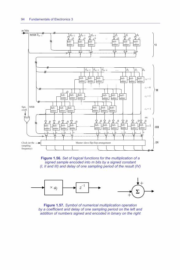
94 Fundamentals of Electronics 3
0 0 0 0 0 0
0
c0 = 1
c1 = 0
c2 = 1
c3 = 1
etc
… δ2 δ1 δ0δm−2 δm−3 δm−4
full-adder
full-adder
full-adder
full-adder
full-adder
half-adder
full-adder
full-adder
full-adder
full-adder
full-adder
full-adder
full-adder
full-adder
half-adder
full-adder
full-adder
half-adder
MSB bm−1 dm−2 dm−3 dm−4 d2 d1 d0
m bits
full-adder
full-adder
full-adder
full-adder
full-adder
half-adder
0 0 0 ... 0 0 1
1 0 1 0 1 0 1 0 1 0 1 0
Sgn. MSBcoeff.
1 0 1 01 0 1 0 1 0 1 01 0 1 0 1 0 1 0
full-adder
full-adder
full-adder
full-adder
full-adder
full-adder
1full-adder
full-adder
full-adder
full-adder
0 0 0 0
Master–slave flip-flop arrangementClock (at thesamplingfrequency)
II
I
III
IV
Figure 1.56. Set of logical functions for the multiplication of a signed sample encoded into m bits by a signed constant
(I, II and III) and delay of one sampling period of the result (IV)
z−1 × aj Σ+
+
Figure 1.57. Symbol of numerical multiplication operation by a coefficient and delay of one sampling period on the left and addition of numbers signed and encoded in binary on the right
Discrete-time Signals and Systems 95
Another solution capable of performing the same operation consists of storing all the results of the product C×D in memory such as a lookup table; the bits of number D are then used as address bits. Such a solution is however likely to require more transistors than the previous one in the silicon wafer. Regardless of the computational method adopted, the basic operators can be symbolized as in Figure 1.57.
In order to achieve an IIR filter, different structures can be employed which make use of the basic operators previously detailed, making it possible to perform the multiplication by a constant, the delay of one sampling period, which is based on an assembly of master–slave flip-flops as in section IV of Figure 1.56, and the addition of signed numbers, summarized by symbols in Figure 1.57.
According to the given expression in 1.4.6.3 in the case where only a second-order transmittance is considered and by normalizing the first coefficient of the denominator of the transmittance to 1, the output is written as follows:
]2[]1[][]2[]1[][ 32132 −+−++−+−= ixbixbixbiyaiyaiy .
To implement a filter of order higher than 2, cascading several second-order sections proves to be a viable solution. If, on the contrary, it is desirable to implement the entire computation related to the full transmittance without breaking it down into second-order sections, the diagrams must be completed at the level of the dashed arrows (Figure 1.58 and 1.59) by adding the branches related to the coefficients b4, b5,… a4, a5 and so on to directly obtain the result given in section 1.4.6.3:
][]2[]1[][][]2[]1[][ 1321132 mixbixbixbixbniyaiyaiyaiy mn −++−+−++−++−+−= ++ .
The system then operates according to an algorithmic sequence taking place following the basic operations arranged vertically in Figure 1.58 and 1.59, which shows other possible algorithms [MAT 94].
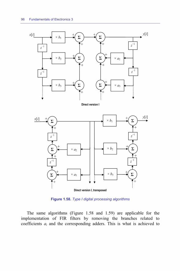
96 Fundamentals of Electronics 3
z−1
× b1 Σ+
+x[i]
z−1
× b2
× b3
Σ+
+
Σ+
+
z−1
Σ+
+
z−1
× a2
× a3
Σ+
+
Σ+
+
y[i]
Direct version I
z−1
× b1 Σ +
+ x[i]
z−1
× b2
× b3
Σ +
+
Σ +
+
× a2
× a3
y[i]
Direct version I, transposed
z−1
Σ+
+
z−1
Σ+
+
Σ+
+
Figure 1.58. Type I digital processing algorithms
The same algorithms (Figure 1.58 and 1.59) are applicable for the implementation of FIR filters by removing the branches related to coefficients ai and the corresponding adders. This is what is achieved to
Discrete-time Signals and Systems 97
implement the improved decimation. In effect, the basic decimation operation, equivalent to subsampling, consists only of taking a sample among N according to a period NTe if Te was the initial period, but it incurs the loss of a huge amount of information since N−1 samples are ignored. In practice, this division of the sample frequency is associated with low-pass filtering allowing for both the recovery of the average value (or the sum) of samples during the interval NTe and the attenuation of the entire portion of the spectrum corresponding to the fluctuations in the amplitude of the samples around this average value. At the same time, the filter implements the anti-aliasing function as a means, before downsampling, to remove in the ideal case or to strongly attenuate the portion of the spectrum that will fold after downsampling (see Figures 1.8 and 1.9). It may be noted that among the FIR filters described in section 1.4.6.5, the Blackman-Harris filter provides the strongest attenuation in stopband but at the expense of a frequency of the first transmission zero twice higher than that of the
Chebyschev filter. Since cutoff frequencies are neighboring 1.56
2ef
N, the
validation of the sampling theorem is not rigorously performed if fe/N is adopted as output sampling frequency. It would be normally preferable to decrease them by a factor of 2 or 4, but this operation would require doubling or quadrupling N. And fourthly, the number of bits with which the result is encoded (often called “resolution”) can be automatically increased following the property described for the basic operator of the multiplication by a coefficient at the beginning of this section (Figure 1.56): if the coefficient is encoded into n bits, which is often taken equal to log2N, and the initial samples into m bits, the result can be encoded into m+n−1 bits at most. All of these properties are used in the sigma-delta converter described in Chapter 2.
The operations necessary for the convolution and correlation computations are similar and can be achieved with the basic operator of Figure 1.56, modified if the multiplicative factor is no longer a constant. In this case, it is enough to add AND gates on the path of the signals so as to either validate the value 0, or the value 1, for each bit cn−1, cn−2, cn−3, ... c2, c1, c0, depending on the value of the multiplication coefficient.
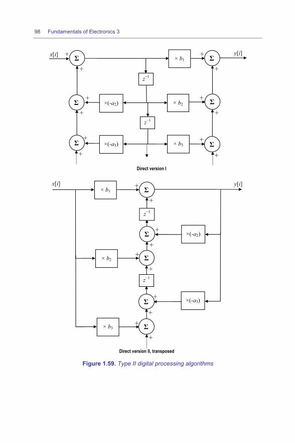
98 Fundamentals of Electronics 3
x[i]
×(-a2)
×(-a3)
Σ+
+
× b2
× b3
Σ+
+
Σ+
+
y[i]
Direct version I
z−1
× b1 Σ+
+x[i]
z−1
× b2
× b3
Σ+
+
Σ+
+
y[i]
Direct version II, transposed
Σ+
+
Σ+
+
z−1
Σ +
+
z−1
Σ +
+
Σ +
+
× b1
×(-a2)
×(-a3)
Figure 1.59. Type II digital processing algorithms
Discrete-time Signals and Systems 99
1.4.7.2. Operations requiring the storage of intermediate results
The operations that require the storage of intermediate results are interpolation or oversampling based on the application of the Shannon formula (see section 1.1.2) and transforms such as DFT, FFT, DCT, MDCT (see section 1.1.3) for the calculation of spectra or their inverses. They can be implemented in real time with the basic functions described in the previous paragraph, provided that functions are added for storing intermediate data that can be achieved by means of a number of shift registers equal to the number of bits utilized. The delay with which the result is output is obviously at least equal to the number of sampling periods needed to perform all operations, but this can still be considered as real-time processing based on operations carried out by an algorithmic system whose rate is imposed by the sampling clock. This option proves interesting if the computational system includes no adjustable parameters and must be fixed by way of cabled logic circuits (usually using a programmable circuit) in its final configuration to deliver a result in real time.
The other way to perform these computations is provided by microprocessors and associated peripherals, and more particularly by computational processors known as DSPs (digital signal processors) or by software running on a computer. Some software programs such as MATLAB and SciLab, are capable of both carrying out the requested operations in RAM in real time and of generating code that will be transferred to ROM in the DSP to turn the application autonomous, which enables development and testing prior to the final implementation. This is the path which is generally chosen if the application has to process pre-recorded data, without any significant constraint on the processing time, or if the computations must be achieved with adjustable parameters that require decision-based choices according to an algorithm involving loops and branches. This is, for example, the case for the search of the maximal correlation between a data set and predetermined templates.
1.5. Discrete-time state-space form
All systems studied in this chapter deal with sampled, analog or digital signals that can be represented by sequences, as described earlier in this chapter. The basic operations present in these systems can be equated to multiplications by a constant, delays of a sampling period Te and summations or differences, following a measurement performed for each
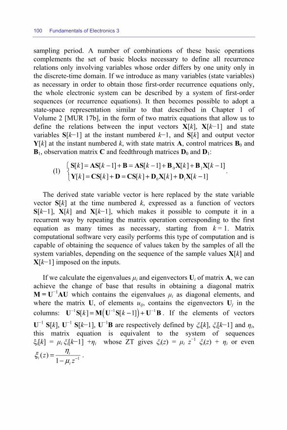
100 Fundamentals of Electronics 3
sampling period. A number of combinations of these basic operations complements the set of basic blocks necessary to define all recurrence relations only involving variables whose order differs by one unity only in the discrete-time domain. If we introduce as many variables (state variables) as necessary in order to obtain those first-order recurrence equations only, the whole electronic system can be described by a system of first-order sequences (or recurrence equations). It then becomes possible to adopt a state-space representation similar to that described in Chapter 1 of Volume 2 [MUR 17b], in the form of two matrix equations that allow us to define the relations between the input vectors X[k], X[k−1] and state variables S[k−1] at the instant numbered k−1, and S[k] and output vector Y[k] at the instant numbered k, with state matrix A, control matrices B0 and B1, observation matrix C and feedthrough matrices D0 and D1:
0 1
0 1
[ ] [ 1] [ 1] [ ] [ 1](1)
[ ] [ ] [ ] [ ] [ 1]k k k k kk k k k k
= − + = − + + − = + = + + −
S AS B AS B X B XY CS D CS D X D X
.
The derived state variable vector is here replaced by the state variable vector S[k] at the time numbered k, expressed as a function of vectors S[k−1], X[k] and X[k−1], which makes it possible to compute it in a recurrent way by repeating the matrix operation corresponding to the first equation as many times as necessary, starting from k = 1. Matrix computational software very easily performs this type of computation and is capable of obtaining the sequence of values taken by the samples of all the system variables, depending on the sequence of the sample values X[k] and X[k−1] imposed on the inputs.
If we calculate the eigenvalues μi and eigenvectors Ui of matrix A, we can achieve the change of base that results in obtaining a diagonal matrix M = U−1AU which contains the eigenvalues μi as diagonal elements, and where the matrix U, of elements uij, contains the eigenvectors Uj in the columns: ( )1 1 1[ ] [ 1]k k− − −= − +U S M U S U B . If the elements of vectors U−1 S[k], U−1 S[k−1], U−1B are respectively defined by ξi[k], ξi[k−1] and ηi, this matrix equation is equivalent to the system of sequences ξi[k] = μi ξi[k−1] +ηi whose ZT gives ξi(z) = μi z−1 ξi(z) + ηi or even
1( )1
ii
i
zz
ηξμ −=
−.
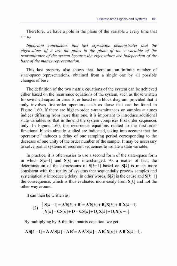
Discrete-time Signals and Systems 101
Therefore, we have a pole in the plane of the variable z every time that z = μi.
Important conclusion: this last expression demonstrates that the eigenvalues of A are the poles in the plane of the z variable of the transmittance of the system because the eigenvalues are independent of the base of the matrix representation.
This last property also shows that there are an infinite number of state-space representations, obtained from a single one by all possible changes of base.
The definition of the two matrix equations of the system can be achieved either based on the recurrence equations of the system, such as those written for switched-capacitor circuits, or based on a block diagram, provided that it only involves first-order operators such as those that can be found in Figure 1.60. If there are higher-order z-transmittances or samples at times indices differing from more than one, it is important to introduce additional state variables so that in the end the system comprises first order sequences only. In Figure 1.60, the recurrence equations related to the first-order functional blocks already studied are indicated, taking into account that the operator z−1 induces a delay of one sampling period corresponding to the decrease of one unity of the order number of the sample. It may be necessary to solve partial systems of recurrent sequences to isolate a state variable.
In practice, it is often easier to use a second form of the state-space form in which S[k−1] and S[k] are interchanged. As a matter of fact, the determination of the expressions of S[k−1] based on S[k] is much more consistent with the reality of systems that sequentially process samples and systematically introduce a delay. In other words, S[k] is the cause and S[k−1] the consequence, which is thus evaluated more easily from S[k] and not the other way around.
It can then be written as:
0 1
0 1
[ 1] [ ] [ ] [ ] [ 1](2)
[ ] [ ] [ ] [ ] [ 1]k k k k kk k k k k
′ ′ ′ ′ ′− = + = + + − = + = + + −
S A S B A S B X B XY CS D CS D X D X
By multiplying by A the first matrix equation, we get:
0 1[ 1] [ ] [ ] [ ] [ 1]k k k k k′ ′ ′ ′ ′− = + = + + −AS A A S AB A A S AB X AB X .
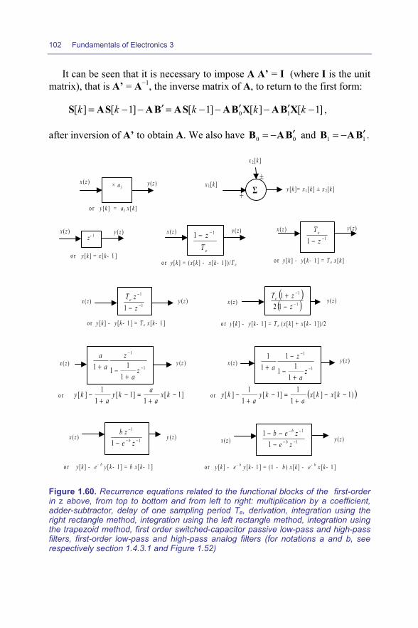
102 Fundamentals of Electronics 3
It can be seen that it is necessary to impose A A’ = I (where I is the unit matrix), that is A’ = A−1, the inverse matrix of A, to return to the first form:
0 1[ ] [ 1] [ 1] [ ] [ 1]k k k k k′ ′ ′= − − = − − − −S AS AB AS AB X AB X ,
after inversion of A’ to obtain A. We also have 0 0′= −B AB and 1 1′= −B AB .
Figure 1.60. Recurrence equations related to the functional blocks of the first-order in z above, from top to bottom and from left to right: multiplication by a coefficient, adder-subtractor, delay of one sampling period Te, derivation, integration using the right rectangle method, integration using the left rectangle method, integration using the trapezoid method, first order switched-capacitor passive low-pass and high-pass filters, first-order low-pass and high-pass analog filters (for notations a and b, see respectively section 1.4.3.1 and Figure 1.52)
× a j Σ±
+
z - 1
eTz 11 −− 11 −− z
T e
o r y [k ] = a j x [k ]
x (z )
x 2 [k ]
y [k ]= x 1 [k ] ± x 2 [k ]
o r y [k ] = x [k - 1 ]o r y [k ] = (x [k ] - x [k - 1 ]) /T e
o r y [k ] - y [k - 1 ] = T e x [k ]
o r y [k ] - e - b y [k - 1 ] = b x [k - 1 ] o r y [k ] - e - b y [k - 1 ] = (1 - b ) x [k ] - e - b x [k - 1 ]
1
1
1 −
−
− zzTe
( )( )1
1
121
−
−
−+
zzT e
o r y [k ] - y [k - 1 ] = T e x [k - 1 ] o r y [k ] - y [k - 1 ] = T e (x [k ] + x [k - 1 ]) /2
1
1
1 −−
−
− zezb
b 1
1
11
−−
−−
−−−
zezeb
b
b
1
1
1111 −
−
+−+ z
a
za
a1
1
111
11
1−
−
+−
−+ z
a
za
o r ]1[1
]1[1
1][ −+
=−+
− kxa
akya
ky o r ( ))1[][1
1]1[1
1][ −−+
=−+
− kxkxa
kya
ky
y (z )
y (z ) y (z ) y (z )
y (z ) y (z )
y (z ) y (z )
y (z ) y (z )
x (z )
x (z ) x (z )
x (z ) x (z )
x 1 [k ]
x (z ) x (z )
x (z ) x (z )
Discrete-time Signals and Systems 103
Provided that the eigenvalues are independent of the chosen base, the comparison of those of A and A’ in a specific base for each representation shows that the eigenvalues of A’ are the inverse of the poles of the system in the plane of the z variable. In the event the notation of the second matrix equation does not appear to be immediate, it is possible to resort to the stationarity property that is always implicitly satisfied in these systems and allows for all the indices of the sequence to be modified by adding or subtracting a unity therefrom. Furthermore, it is useful to calculate the inverse of matrix A or A’ in order to ensure that it is not singular. In fact, a singular matrix indicates that the number of state variables that have been chosen is too high and that these variables are not all independent, which must lead to the revision of the system of recurrence equations.
In conclusion, the representation based on state variables allows us to model all the stationary sampled systems, analog or digital, verifying the sampling theorem, and to obtain the evolution of the sequences of samples of the state variables and on output, usually by employing software for systems of order >2. The calculation method is simpler than in the continuous-time state-space representation as it only requires that stages be concatenated consisting, after each evaluation of S[k] and Y[k], in inserting the result in the second member of the matrix system (1) from k=1 and to iterate. The input variables are the initial data that make it possible for each step to completely evaluate the second member. It is even possible to address the case in which the sampling period is not constant (frequency modulated signals) by adapting the coefficients of the matrices at every computation step and this process can also be applied to systems including blocks having a nonlinear response. In both cases, some matrix coefficients become dependent of state variables and require that they be reexamined and eventually modified at each computational time step. The simulation and analysis of the responses of these systems can be performed by means of software programs (MATLAB, SciLab, etc.) based on a block diagram built using predetermined functional blocks whose parameters have to be detailed (Simulink, xcos, etc.), and that are able to simulate any elementary function that may exist. Finally, by solving one of the two systems of equations, which requires that A or A’ be diagonalized, it is possible to express an output variable after replacement of the state variables according to the input variables at different times. Then by taking the ZT of this recurrence relation, we can deduce the transfer function of this system in the plane of the z variable and the eigenvalues of A or A’ give direct access to the poles of the transmittance.

104 Fundamentals of Electronics 3
1.6. Exercises
1.6.1. Switched-capacitor first-order high-pass filter
Type P and I switches (MOS transistor-based) are respectively closed (switched on) when the command is 1 and open (switched off) when it is zero, corresponding to P in phase with integer times (k − 1)Te, kTe and so on, and I in inverted phase; in other words closed in synchronism with half-integer times (k − 1/2)Te, (k +1/2)Te and so forth. They are “break before make” switches, in such a way that opening happens just before closing.
PS E
C2 = aC I
Q1
Q2 i2
i1 0
P
I
k − 1 k − 1/2 k k + 1/2 t / Te
1
0
1
0
1) Write the equations connecting the charges Q1 and Q2 to voltages E and S for the circuit at time indices k − 1, k − 1/2 and k: Q1[k − 1], Q2[k − 1], Q1[k − 1/2] and so on, as a function of E[k − 1], S[k− 1], E[k − 1/2] and so forth. Also write the relations of charge conservation during the transitions at time indices k − 1/2 and k. Deduce, by eliminating the quantities evaluated at k − 1/2, the recurrence relation between E[k− 1], S[k− 1], E[k] and S[k].
C1 = C
Discrete-time Signals and Systems 105
2) Determine the transmittance in z of the assembly T2(z) = S(z)/E(z) from
the ZT of the previous equation. The parameter a
b+
=1
1 < 1 can be used.
3) Determine the samples of the step response SU(z), that is when
111)( −−
=z
zE , by carrying out the division of the numerator by the
denominator of SU(z) = T2(z)E(z). What is the initial value and toward what final value does it converge?
4) For sinusoidal signals z = exp(jωTe) and if ωTe << 1, it can be written at the first order that z−1 = 1 − jωTe . In this case, determine T2(jω), the nature of this transmittance and the associated time constant. What must be the condition upon a in order for this approximation to be still valid at the cutoff angular frequency? If it is satisfied, is the sampling theorem respected at the cut-off frequency?
Answers:
1) The equations are of the Q=CV and charge conservation types:
a) At time index k − 1:
Q1[k−1] = C(S[k−1] − E[k−1]);
Q2[k−1] = aC S[k−1].
b) At time k−1/2, switch P switches off (opening) and therefore, the charge Q1 does not change:
Q1[k −1/2] = Q1[k − 1].
In addition:
Q1[k−1/2] = C(S[k−1/2] − E[k−1/2])
and Q2[k −1/2] = 0, because C2 is shortly circuit by the switch I which is closing (switching on).
106 Fundamentals of Electronics 3
Therefore it can be inferred that
S[k−1/2] − E[k−1/2] = S[k−1] − E[k−1].
c) At time index k:
Q1[k] = C ( S[k] − E[k] );
Q2[k] = aC S[k].
At the transition k−1/2 → k:
[ ] [ ] [ ] [ ]2/12/10)( 22112/1
21 −−+−−==+−
kQkQkQkQdtiik
k
involving 0 = S[k] − E[k] + a S[k] – (S[k−1] − E[k−1]) from which the recurrence relation is deduced:
(1 + a) S[k] − S[k−1] = E[k] − E[k−1].
2) The ZT gives: (1 + a) S(z) − z−1 S(z) = E(z) − z−1 E(z)
(1 + a − z−1) S(z) = (1 − z−1) E(z).
By establishing ab += 11 : T2(z) 1
1
11
)()(
−
−
−−==
zbzbzE
zS .
3) With 111)( −−
=z
zE , we get: 11
1
1 11
11
11)( −−
−
− −=
−−
−=
zbb
zbzb
zzSu
.
According to the initial value theorem, the sample SU[0] is obtained from SU(z) when z → ∞, which gives SU[0] = b.
By division:
( ) ++++=++++= −−−−−− 3423123211)( zbzbzbbzbzbzbbzSU
corresponding to samples SU[0] = b ; SU[1] = b2 ; SU[2] = b3 ; … ; SU[k] = bk+1.

Discrete-time Signals and Systems 107
Given that b < 1, this series tends to zero and thus reproduces well the step response of a high-pass filter:
k
Su[k]
0
b
4) For sinusoidal signals z = exp(jωTe) and if ωTe << 1, it can be written as z−1 = 1 − jωTe at first order with a relative error smaller than 2% if ωTe < 4; hence:
aT
j
aT
jbTjb
TjbjT
e
e
e
e
ω
ωω
ωω
+=+−=
11)(2
.
that is, the transfer function of a high-pass filter of time constant Te/a. However, in order for this approximation to be applicable to ωc = a/Te , it is
necessary that ωcTe << 1 thereby a << 1. In this case 21
2ec
cf
f ππω
<<=
and the sampling theorem is respected.
1.6.2. Basic switched-capacitor-based filter operator (IIR) using an ideal operational amplifier.
Same functioning conditions of the P- and I-type switches (MOS transistor-based) as in exercise 1.6.1.
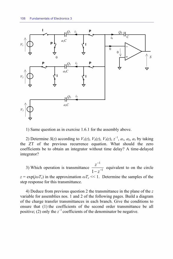
108 Fundamentals of Electronics 3
Pa1C
S
V1
C
I Q1 Q0 i1
V2
V3
I
P
a2C
Q2 i2
0
I
PP
I
Q3 i3
a3C
−
+ 0
i0
0
1) Same question as in exercise 1.6.1 for the assembly above.
2) Determine S(z) according to V1(z), V2(z), V3(z), z−1, a1, a2, a3 by taking the ZT of the previous recurrence equation. What should the zero coefficients be to obtain an integrator without time delay? A time-delayed integrator?
3) Which operation is transmittance 1
1
1 −
−
− zz
equivalent to on the circle
z = exp(jωTe) in the approximation ωTe << 1. Determine the samples of the step response for this transmittance.
4) Deduce from previous question 2 the transmittance in the plane of the z variable for assemblies nos. 1 and 2 of the following pages. Build a diagram of the charge transfer transmittances in each branch. Give the conditions to ensure that (1) the coefficients of the second order transmittance be all positive; (2) only the z−1 coefficients of the denominator be negative.

Discrete-time Signals and Systems 109
Pa1C
S
C
I
E
I
P
a2CI
PP
I
a3C
−
+ 0
0
a4C PP
I I
Assembly no. 1
Assembly no. 2: see Figure 1.49.
Answers:
1) The equations are of the Q=CV and charge conservation types:
a) At time index k − 1:
Q0[k −1] = −C S[k−1],
Q1[k −1] = 0,
Q2[k −1] = −a2 C V2[k −1],
Q3[k −1] = −a3 C V3[k −1].
b) At time index k− 1/2:
Q0[k −1/2] = −C S[k −1/2],
Q1[k −1/2] = −a1 C V1[k −1/2],
Q2[k −1/2] = 0,
Q3[k −1/2] = −a3 C V3[k −1/2].

110 Fundamentals of Electronics 3
During the transition from k − 1 to k −1/2
( ) [ ] [ ] [ ] [ ]2/12/1110)( 03032/1
103
2/1
103 −−−−−+−=+−==+ −
−
−
− kQkQkQkQQQdtii k
k
k
k
involving: a3 ( V3[k −1/2] − V3[k −1] ) + S[k −1/2] − S[k −1] = 0.
c) At time k:
Q0[k] = −C S[k],
Q1[k] = 0,
Q1[k] = −a2 C V2[k],
Q3[k] = −a3 C V3[k].
During the transition from k − 1/2 to k
( )kk
k
k
QQQQdtiiii 2/132102/1
3210 0)( −−
+++−==+++−
involving:
0 = S[k] − S[k −1/2] − a1 V1[k −1/2] + a2(V2[k] − 0) + a3 (V3[k] − V3[k −1/2]).
Nonetheless, according to the transition from k − 1 to k −1/2,
a3 V3[k −1/2] + S[k −1/2] = a3 V3[k −1] + S[k −1], giving after substitution:
S[k] = S[k −1] + a1 V1[k −1/2] − a2 V2[k] − a3( V3[k] − V3[k −1] ).
2) For the sampling theorem to be applied, the voltages must not vary much between the half sampling periods. It may thus be considered that V1[k −1/2] = V1[k −1], which amounts to considering integer index times only for the observation of voltages (if this approximation is not to be carried out, the factor z−1/2 will be used instead of z−1 for this term in the ZT). The ZT of the recurrence equation then gives:
S(z) = z−1 S(z) + a1 z−1 V1(z) − a2 V2(z) − a3 (1 − z−1) V3(z) .

Discrete-time Signals and Systems 111
Hence finally:
)()(1
1)(1
)( 3321211
1
1 zVazVz
azVz
zazS −−
−−
= −−
−.
For a non-delayed integrator, branches 1 and 3 are removed (a1 = 0, a3 = 0) and for a delayed integrator, the branches 2 and 3 are removed (a2 = 0, a3 = 0).
3) If z = exp(jωTe) and ωTe << 1, we get z ≈ 1 + jωTe and z−1 ≈ 1 − jωTe
at first order; then eTjzz
zω1
11
1 1
1
≈−
=− −
−
corresponds to integration in the
time domain (when ωTe << 1, there is also not much difference between
1
1
1 −
−
− zz
and 111
−− z). More accurately,
e
e
TjTj
zz
z ωω+≈
−=
− −1
111
1 is
equivalent to the inverse transmittance of a high-pass filter, but this only makes sense for ω << 1/Te so as to ensure that ωTe << 1 and in this approximation there is no difference between both integrators.
For the step response, we multiply by the ZT of the unit step 111
−− z and
the division of the numerator by the denominator according to the increasing powers of z-1 is performed. Concerning the transmittance 11
1−− z
, the ZT of
the step response is thus ( ) 2121 211
11
−−− +−=
− zzz, which gives
1 + 2 z−1 + 3 z−2 + 4 z−3 + … + (n+1) z−n corresponding to a series of successive
samples 1 ; 2 ; 3 ; … ; n+1, from time zero. For the response ( )21
1
1 −
−
− zz , the
delay theorem simply has to be applied and the whole previous series is delayed by one sample step, or more precisely 0 ; 1 ; 2 ; …n from time zero. Alternatively, a vertical translation of the samples can also be achieved to move
from one series to the other by observing that 11
11 11
1−
−=
− −−
−
zzz .
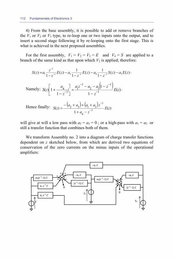
112 Fundamentals of Electronics 3
4) From the base assembly, it is possible to add or remove branches of the V1 or V2 or V3 type, to re-loop one or two inputs onto the output, and to insert a second stage following it by re-looping onto the first stage. This is what is achieved in the next proposed assemblies.
For the first assembly, V1 = V2 = V3 = E and V4 = S are applied to a branch of the same kind as that upon which V2 is applied; therefore:
)()(1
1)(1
1)(1
)( 314121
1
1 zEazSz
azEz
azEz
zazS −−
−−
−−
= −−−
−.
Namely: ( ))(
1
1
11)( 1
132
11
14 zE
z
zaaza
z
azS −
−−
− −
−−−=
−+ .
Hence finally: ( ) ( ))(
1)( 1
4
13132 zE
za
zaaaazS −
−
−+
+++−=
will give at will a low pass with a2 = a3 = 0 ; or a high-pass with a1 = a2 or still a transfer function that combines both of them.
We transform Assembly no. 2 into a diagram of charge transfer functions dependent on z sketched below, from which are derived two equations of conservation of the zero currents on the minus inputs of the operational amplifiers:
E
+ +
+ + a3(z−1−1) C
a1 z−1 C (z−1−1) C
−a5 C
S1 a2 z−1 C
+ +
+ +a4(z−1−1) C
(z−1−1) C
−a7 C
S2
0
0
−a6 C +
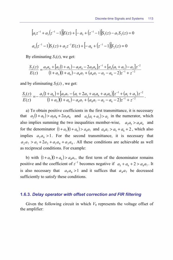
Discrete-time Signals and Systems 113
( )[ ] ( )[ ] 0)()(1)(1 2711
51
31
1 =−−+−+−+ −−− zSazSzazEzaza
( ) ( )[ ] 0)(1)()(1 21
61
211
4 =−+−++− −−− zSzazEzazSza
By eliminating S1(z), we get:
( )[ ] ( )[ ]( )( ) ( ) 21
65747465
22314
1434152432
21121
)()(
−−
−−
+−−−+−++−++−−++=
zzaaaaaaaazaaaazaaaaaaaa
zEzS
and by eliminating S2(z) , we get:
( ) ( )[ ] ( )( )( ) ( ) 21
65747465
231
163613172631
21121
)()(
−−
−−
+−−−+−+++++++−++−=zzaaaaaaaa
zaazaaaaaaaaaazEzS .
a) To obtain positive coefficients in the first transmittance, it is necessary that ( ) 434152 21 aaaaaa +>+ and ( ) 2314 aaaa >+ in the numerator, which also implies summing the two inequalities member-wise, 4352 aaaa > and for the denominator ( )( ) 7465 11 aaaa >++ and 26574 ++> aaaa , which also implies 165 >aa . For the second transmittance, it is necessary that
63613172 2 aaaaaaaa +++> . All these conditions are achievable as well as reciprocal conditions. For example:
b) with ( )( ) ,11 7465 aaaa >++ the first term of the denominator remains positive and the coefficient of z−1 becomes negative if 7465 2 aaaa >++ . It is also necessary that 165 >aa and it suffices that 74aa be decreased sufficiently to satisfy these conditions.
1.6.3. Delay operator with offset correction and FIR filtering
Given the following circuit in which V0 represents the voltage offset of the amplifier:
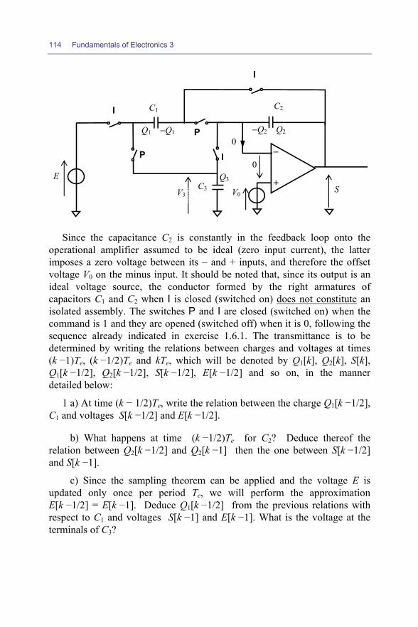
114 Fundamentals of Electronics 3
−Q2 Q2
I
C3 S E
P
C2 I
P − +
0
0 Q1 −Q1
V0
I
C1
Q3
V3
Since the capacitance C2 is constantly in the feedback loop onto the operational amplifier assumed to be ideal (zero input current), the latter imposes a zero voltage between its – and + inputs, and therefore the offset voltage V0 on the minus input. It should be noted that, since its output is an ideal voltage source, the conductor formed by the right armatures of capacitors C1 and C2 when I is closed (switched on) does not constitute an isolated assembly. The switches P and I are closed (switched on) when the command is 1 and they are opened (switched off) when it is 0, following the sequence already indicated in exercise 1.6.1. The transmittance is to be determined by writing the relations between charges and voltages at times (k −1)Te, (k −1/2)Te and kTe, which will be denoted by Q1[k], Q2[k], S[k], Q1[k −1/2], Q2[k −1/2], S[k −1/2], E[k −1/2] and so on, in the manner detailed below:
1 a) At time (k − 1/2)Te, write the relation between the charge Q1[k −1/2], C1 and voltages S[k −1/2] and E[k −1/2].
b) What happens at time (k −1/2)Te for C2? Deduce thereof the relation between Q2[k −1/2] and Q2[k −1] then the one between S[k −1/2] and S[k −1].
c) Since the sampling theorem can be applied and the voltage E is updated only once per period Te, we will perform the approximation E[k −1/2] = E[k −1]. Deduce Q1[k −1/2] from the previous relations with respect to C1 and voltages S[k −1] and E[k −1]. What is the voltage at the terminals of C3?

Discrete-time Signals and Systems 115
2 a) At time kTe, what value does charge Q1[k] assume?
b) Write the charge conservation on the armatures of capacitors C1-C3 and C1-C2 which are in contact during the transition at instant kTe as well as the relations between charges and potentials in C2. Deduce thereof V3[k] − V0 and Q1[k] as a function of C1, C2, C3, S[k] and S[k −1] .
c) According to the previous equations, establish the relation between S[k], S[k −1] and E[k −1] and show that it is correctly independent of V0.
3) We define a = C2/C1. Establish the expression of the transmittance T(z) = S(z)/E(z) for any a.
4) By taking C3 = C1, determine C2 so that T(z) is equivalent to a simple delay of the input signal of one period Te. What is the function of M identical circuits arranged in cascade?
5) It is assumed that the sum of the M output voltages is performed with an identical weighting for each one (comb filter). Establish the ZT of the output of the adder Scb(z) according to E(z) and express the transmittance in a compact form with respect to z, and then with respect to ωTe in the case of a sinusoidal input of frequency f << fe/2 = 1/(2Te).
Answers:
1) a) At time (k −1/2)Te, Q1[k −1/2] = C1 (E[k −1/2] − S[k −1/2] ),
b) and the capacitor C2 is isolated because of the zero input current of the operational amplifier; therefore, Q2[k −1/2] = Q2[k −1]; S[k −1/2] = S[k −1] and Q2[k −1/2] = C2( S[k −1] − V0 ).
c) The potential differences at the terminals of C1 and C3 are such that Q1[k − 1/2] = C1 (E[k − 1] − S[k − 1] ) and V3[k − 1/2] = V0; hence Q3[k − 1/2] = C3V0.
2) a) At time kTe, closing the two switches P located between C1 and C3 yields
Q1[k ] = C1(V3[k] − V0).
116 Fundamentals of Electronics 3
b) The left armature of C1 and the upper armature of C3 form an isolated single system, with the right armature of C1 at voltage V0. Therefore,
Q1[k ] + Q3[k ] − Q1[k − 1/2] − Q3[k − 1/2] = 0;
hence C1(V3[k] − V0) + C3(V3[k] − V0) − C1( E[k − 1] − S[k − 1] ) = 0.
Therefore ( )]1[][][31
203 −−
+=− kSkS
CCCVkV and ( )]1[][][
31
211 −−
+= kSkS
CCCCkQ .
In addition, the armatures of C1 and C2 are put in contact through the switch P and are isolated; therefore Q1[k] − Q1[k − 1/2] + Q2[k] − Q2[k − 1/2] = 0. Since the operational amplifier imposes voltage V0 on the left armature of C2, we also get Q2[k ] = C2 ( S[k ] − V0 ).
c) We deduce by substituting in the second charge conservation equation: ( ) ( ) ( ) ( ) 0]1[][]1[]1[]1[][ 02021
31
21 =−−−−+−−−−−−+
VkSCVkSCkSkECkSkSCC
CC ,
from which it can be inferred that
]1[]1[][ 11231
212
31
21 −=−
−+
+−
+
+kECkSCC
CCCCkSC
CCCC .
3) The ZT is therefore:
)()(1)( 11
31
2
31
2 zEzzSzaCC
CzSaCC
C −− =
−+
+−
+
+
or:
1
31
2
31
2
1
1
)()(−
−
−+
+−
+
+
=za
CCCa
CCC
zEzzS .
4) In order for S(z) = z−1 E(z), it is necessary
that( )
+
+==
+
+ 131
312
31
2 21CCC
CCCaCC
C . Hence the condition
( ) ( )312131 2 CCCCCC +=+ . If we take C3 = C1, 3
2 12
CC = and 32
1
2 ==CCa
have to be imposed.
Discrete-time Signals and Systems 117
The input signal is thus delayed by one sample period, and by arranging M stages in cascade, we can obtain the input signal delayed by kTe on output of the k-th stage, with k ∈ [0 , M], like in a shift register for a binary logic signal.
5) We have 1
)1(
0 11)()()( −
+−−
−−== z
zzEzzEzSM
M kcb and by
substituting z−1 by e−jωTe : ( )( )e
ep Tj
TMjzEjSω
ωω−−
+−−=
exp1)1(exp1)()( namely a
transmittance in sinusoidal regime ( )( ) ( )e
e
e fTjMfT
fTM ππ
π −+ expsin
)1(sin
provided that f < fe/2 be satisfied, of the low-pass type with a “gain” M +1 when f → 0, which is the result of the summation of the input and of the M outputs.
The transmittance is 0 for 1)1( +
=+
=M
fkTM
kf e
ek (the integer
k ∈ [0 , M/2]) and the complex exponential factor involves a delay 2
eMT .
1.6.4. Phase-locked loops
The algebraic phase difference ϕ between the signals s1(t) and s2(t) can be considered as the difference of the instantaneous phase of either one, that is ϕ1(t) − ϕ2(t), determined from the time interval Δt between rising edges. The measurement is carried out by the charge or discharge of a capacitor C0 with constant current during the fraction Δt of the period by the circuit shown on the next page, itself controlled by the sequential logic circuit described in the course (Figure 1.25).
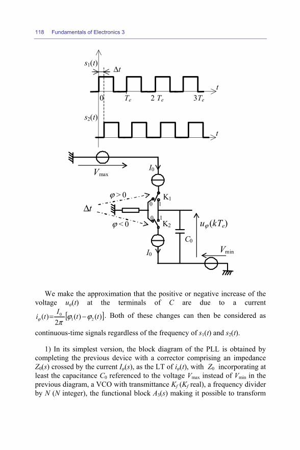
118 Fundamentals of Electronics 3
s1(t)
0 Te 2 Te 3Te t
t
s2(t)
Δt
I0
Δt
uϕ (kTe) C0
I0
K1
K2
0 1
0 1
ϕ > 0
ϕ < 0
Vmax
Vmin
We make the approximation that the positive or negative increase of the voltage uφ(t) at the terminals of C are due to a current
[ ])()(2
)( 210 tt
Iti ϕϕ
πϕ −= . Both of these changes can then be considered as
continuous-time signals regardless of the frequency of s1(t) and s2(t).
1) In its simplest version, the block diagram of the PLL is obtained by completing the previous device with a corrector comprising an impedance Z0(s) crossed by the current Iφ(s), as the LT of iφ(t), with Z0 incorporating at least the capacitance C0 referenced to the voltage Vmax instead of Vmin in the previous diagram, a VCO with transmittance Kf (Kf real), a frequency divider by N (N integer), the functional block A3(s) making it possible to transform
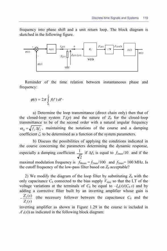
Discrete-time Signals and Systems 119
frequency into phase shift and a unit return loop. The block diagram is sketched in the following figure.
Z0(s) Z0(s) Iφ(s)
Kf
F3(s) Iϕ(s) 0 A0(s)
ϕ2(s)
−
+ A3(s)
VCO
ϕ1(s) ϕ2(s) / N
F3(s)/N
Reminder of the time relation between instantaneous phase and frequency:
=t
dttft0
')'(2)( πϕ .
a) Determine the loop transmittance (direct chain only) then that of the closed-loop system T1(p) and the nature of Z0 for the closed-loop transmittance to be of the second order with a natural angular frequency
221 ffn Δ=ω , maintaining the notations of the course and a damping coefficient ζ1 to be determined as a function of the system parameters.
b) Discuss the possibilities of applying the conditions indicated in the course concerning the parameters determining the dynamic response, especially a damping coefficient
21 if Δf2 is equal to f2max/10 and if the
maximal modulation frequency is fMmax = f2max/100 and f2max= 100 MHz. Is the cutoff frequency of the low-pass filter based on Z0 acceptable?
2) We modify the diagram of the loop filter by substituting Z0 with the only capacitance C0 connected to the bias supply Vmax so that the LT of the voltage variations at the terminals of C0 be equal to –Iφ(s)/(C0 s) and by adding a corrective filter built by an inverting amplifier whose gain is
)()(
1
2
sZsZ− (the necessary follower between the capacitance C0 and the
inverting amplifier as shown in Figure 1.29 in the course is included in A'1(s)) as indicated in the following block diagram:
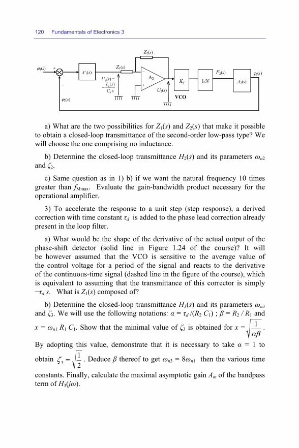
120 Fundamentals of Electronics 3
Z1(s)
Z2(s)
Kf
F2(s) Uϕ(s) =
sCsI
0
)(ϕ− U2(s)
A'1(s)
ϕ2(s)
−
+
A3(s)
VCO
ϕ1(s) ϕ2(s)
1/N
− Α2
+
a) What are the two possibilities for Z1(s) and Z2(s) that make it possible to obtain a closed-loop transmittance of the second-order low-pass type? We will choose the one comprising no inductance.
b) Determine the closed-loop transmittance H2(s) and its parameters ωn2 and ζ2.
c) Same question as in 1) b) if we want the natural frequency 10 times greater than fMmax. Evaluate the gain-bandwidth product necessary for the operational amplifier.
3) To accelerate the response to a unit step (step response), a derived correction with time constant τd is added to the phase lead correction already present in the loop filter.
a) What would be the shape of the derivative of the actual output of the phase-shift detector (solid line in Figure 1.24 of the course)? It will be however assumed that the VCO is sensitive to the average value of the control voltage for a period of the signal and reacts to the derivative of the continuous-time signal (dashed line in the figure of the course), which is equivalent to assuming that the transmittance of this corrector is simply −τd s. What is Z1(s) composed of?
b) Determine the closed-loop transmittance H3(s) and its parameters ωn3 and ζ3. We will use the following notations: α = τd /(R2 C1) ; β = R2 / R1 and
x = ωn1 R1 C1. Show that the minimal value of ζ3 is obtained for x =αβ1 .
By adopting this value, demonstrate that it is necessary to take α = 1 to
obtain 21
3 =ζ . Deduce β thereof to get ωn3 = 8ωn1 then the various time
constants. Finally, calculate the maximal asymptotic gain Am of the bandpass term of H3(jω).
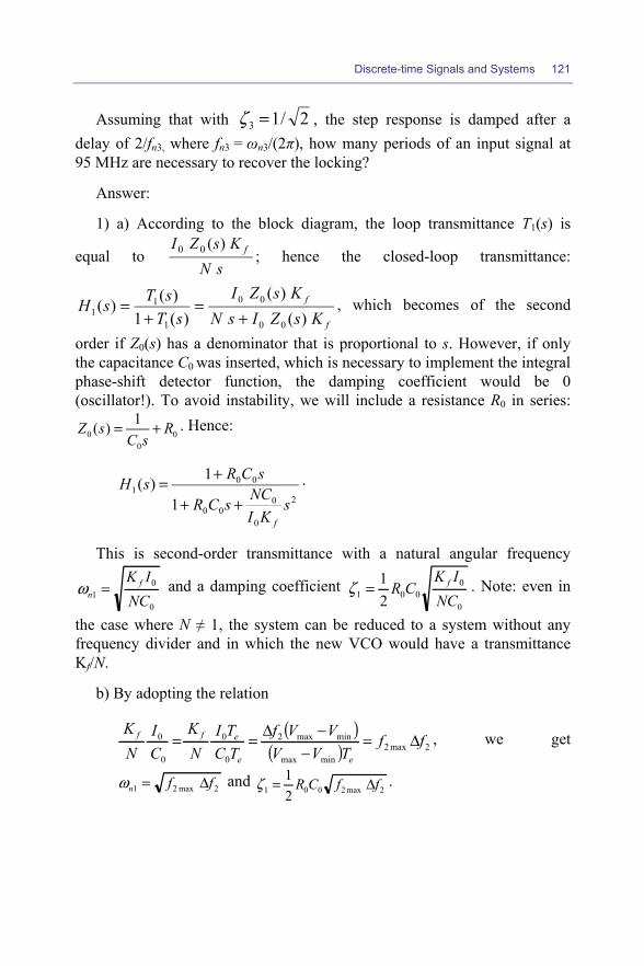
Discrete-time Signals and Systems 121
Assuming that with 2/13 =ζ , the step response is damped after a delay of 2/fn3, where fn3 = ωn3/(2π), how many periods of an input signal at 95 MHz are necessary to recover the locking?
Answer:
1) a) According to the block diagram, the loop transmittance T1(s) is
equal to sN
KsZI f)(00 ; hence the closed-loop transmittance:
f
f
KsZIsNKsZI
sTsTsH
)()(
)(1)()(
00
00
1
11 +
=+
= , which becomes of the second
order if Z0(s) has a denominator that is proportional to s. However, if only the capacitance C0 was inserted, which is necessary to implement the integral phase-shift detector function, the damping coefficient would be 0 (oscillator!). To avoid instability, we will include a resistance R0 in series:
0 00
1( )Z s RC s
= + . Hence:
2
0
000
001
1
1)(s
KINCsCR
sCRsH
f
++
+= .
This is second-order transmittance with a natural angular frequency
0
01 NC
IK fn =ω and a damping coefficient
0
0001 2
1NC
IKCR f=ζ . Note: even in
the case where N ≠ 1, the system can be reduced to a system without any frequency divider and in which the new VCO would have a transmittance Kf/N.
b) By adopting the relation
( )( ) 2max2
minmax
minmax2
0
0
0
0 ffTVV
VVfTCTI
NK
CI
NK
ee
eff Δ=−
−Δ== , we get
2max21 ffn Δ=ω and 2max2001 2
1 ffCR Δ=ζ .
122 Fundamentals of Electronics 3
Numerical application: ==π
ω2
11
nnf 5 MHz and it is thus necessary that
0 0 72
3.15 10R C = =
×45 ns. The first-order filtering of the current I0 is thus
achieved with this time constant, or more specifically a 3.5 MHz cutoff frequency that is not adjustable. However, since the harmonics of the output current of the phase-shift detector are at least at frequencies f2min = 90 MHz and multiples, the filtering is absolutely correct. The frequency fn1 is five times greater than fMmax, which also seems reasonable. On the other hand, if we wanted to accelerate the loop response even further, it would be necessary to increase ωn1 by increasing I0 (or decreasing C0), which would have the disadvantage of limiting the range of linear operation of the phase-shift detector at a value less than 2π.
2) a) We now have:
20 20 2 12
2 2 20 1 0 1 1
( ) ( )( ) 2( )2 ( ) ( ) ( )
f f nK I Z s KI Z sZ sT sC s Z s N s C Z s Ns Z s s
ωππ
= = = .
To obtain a non-zero closed-loop damping coefficient, we have the choice between Z2 including an inductance and a resistance in series and Z1 = R1, or alternatively Z2 = R2 and a capacitance C1 in series with a resistance R1 for Z1. We thus choose the second option, devoid of inductance, which gives:
2212
12112
221
21
221
2
22
1
1)()(1
)()(s
RR
CRsRssZ
RsT
sTsH
nn
n
n
ωωω
ω
++=
+=
+= , namely a
natural angular frequency 2max2
1
2
1
212 ff
RR
RR
nn Δ== ωω and a
damping coefficient 2max21211121
22 2
1121
ffRRCCRRR
n Δ==
ωζ , adjustable
independently of the sensitivity of the phase-shift detector. If we want ωn2 = 2 ωn1 ( fn2 =10 fMmax = 10 MHz) and
21
2 =ζ , then R2 = 4R1 and
=11CR 11,2 ns, corresponding to 14 MHz for the cutoff frequency of the filtering of the current Iφ(s). The closed-loop transmittance is now purely of the low-pass type.
Discrete-time Signals and Systems 123
3) a) The derivative of the actual output of the phase-shift detector is a sequence of impulses smaller than the period except if the loop is completely unlocked. In order for us to continue within the context of a linear approximation, it will be assumed that the VCO reacts to the average value over a period of this signal, which is equivalent to considering the transmittance −τd p. It is theoretically obtained by adding a capacitance Cd = R2 /τd in parallel to the R1-C1 series network, hence the new expression of Z1(s) in the computation of U2(s) that follows (for the practical solution, see section 1.3.3).
b) Now we have 22
01
1
( )( ) 1 d
I s RU s sC R
C s
φ τ
= − + +
and
21 2
3 2
11
( ) 1n
dRT s s
s RC s
ω τ
= + +
for the loop transmittance, from which it is
deduced in closed loop:
( ) 23
2
33
3
2112
211
12
2111
12
11
3
33
21
1
/11
1
)(1)()(
nn
nm
ndd
nd
d
d
ss
sA
CRsCRs
CRCR
sCRCR
sTsTsH
ωωζ
ω
ωττωτ
ττ
++
+=
++
+++
++
=+
=
with αβωτωω +=+= 1111
1213 n
dnn CR
CR ; αωβα
β +=
11 111 n
mCRA
and

124 Fundamentals of Electronics 3
The derivative of the bracket with respect to x is 0 for x =αβ1 ; the
bracket is then equal to αβ2 , that is α = 1 to obtain21
min33 == ζζ .
To obtain ωn3 = 8ωn1, it is then necessary that β = 32, that is R2 = 32 R1.
The time constants are inferred from ωn1 = 3.14×10⁷ rad/s, giving R1 C1 = 5.6 ns and τd = R2 Cd = R2 C1 = 180 ns. We then get a natural frequency fn3 = 8 fn1 = 40 MHz, which significantly approaches
min2max2 ff = 94.8 MHz while maintaining an optimal damping factor. The maximal asymptotic gain of the bandpass part of H3(s) is equal to
21
1=
+=
αα
mA , which provides a contribution close to that of the
low-pass term, thus improving the speed of the step response and therefore the flexibility of the loop. The step response is damped in 2/(40 MHz), or 50 ns, which represents only about five periods of the input signal to restore the lock.
1.6.5. Sampled models of the PLL
By means of initially removing the correction proportional to the phase shift, it has been shown in the previous exercise (question 2) that an effective loop filter was that of the Figure 1.29 with Z2 = R2 and Z1 comprising a resistance R1 in series with a capacitance C1.
1) a) Under these conditions, determine the transmittance G(s) of this loop filter, the shape of its asymptotic Bode diagram and the type of correction that it achieves.
b) Determine what switched-capacitor-based assembly can be achieved by adopting one of the inputs of the basic first-order filtering operator (switched-capacitor-based) of exercise 1.6.2 as input to the filter and by connecting the other two inputs to its output, such that to obtain a filter whose frequency response G1(z) satisfies the same conditions as G(jf)
Discrete-time Signals and Systems 125
in the neighborhood of f → 0 and f = fe/2, assuming fe/2 as being much larger than the frequency of slope break of |G(jf)|.
c) Based on G(s), determine the expression G2(z) of the transmittance of the filter in the domain of the z variable according to the elements of the filter and to ωbl through the modified bilinear transformation, where ωbl is the multiplicative factor in this transformation (same notation as in section 1.4.6.2).
d) From G(s), determine the expression G3(z) of the transmittance of this filter in the domain of the z variable in the approximation of the preserved impulse response. Compare G1(z), G2(z) and G3(z), and give a general expression that can represent the three transfer functions using four real and positive parameters, b1, b2, b3 and b4.
2) Draw the block diagram and establish the transfer function in z of the PLL by adding the correction proportional to the phase shift of question 3 of the previous exercise, as well as the other functional blocks. Give the expression of the transfer function in z of the open-loop T(z) and closed-loop H(z).
Answers:
1) a) We have an inverter arrangement using operational amplifiers
with Z2 = R2 and 11
11)( R
sCsZ += . Hence a gain
sCRsCRsG11
12
1)(
+−= , which
corresponds to a phase-leading or high-pass correction filter.
The Bode diagram of |G(jf)| comprises an asymptote of positive slope +1 in log-log scale or +20 dB/decade in semi-log scale, and a horizontal asymptote beyond the frequency 1/(2πR1C1), with a modulus equal to R2/R1.
b) For f → 0, we have at first-order z−1 = exp(−j2πf /fe) ≈ 1 − j2πf /fe . It is thus necessary that 1 − z−1 be present in the numerator to obtain a transmittance proportional to f in low frequencies. To this end, we adopt as input E(z)=V3(z) and we link V1(z) and V2(z) to S(z) in the first diagram of
exercise 1.6.2, which gives: 1
12
13
1 )1(1)1(
)()()( −
−
+−+−==
zaaza
zEzSzG .

126 Fundamentals of Electronics 3
For f → 0, e
ef ffajaa
ffajjfG/)1(2
/2)(112
301 ++−
=→ π
π is obtained, which gives a
transmittance of the same type as G(jf) but of opposite sign given that we take a2 > a1.
For f = fe/2, z−1 = exp(−jπ) = −1, from which it is deduced that
12
31 2
2)2/(aa
ajfG e ++= which is real such as the high-frequency asymptote
of G(jf) and always positive. This justifies the previous condition that would cause a change of sign not present in G(jf) if it were not satisfied. We will just take the precaution to change the reference voltage of the phase-shift detector in order to find again the plus sign of question 1 in the previous exercise.
c) As part of the modified bilinear transformation, the variable s of
the transmittance G(s) is replaced by 11
+−
zz
blω , where
=
e
c
cbl
ff
f
π
πωtan
2 , to
cancel the error in the frequency at the frequency fc = 1/(2πR1C1), which yields:
11111
112
11
12
2 )1(1)1(
111
11
)( −
−
−++−−=
+−+
+−
−=zCRCR
zCR
zzCR
zzCR
zGblbl
bl
bl
bl
ωωω
ω
ω.
d) For the high-pass filter, the impulse response is given following the table of section 1.4.2 by δ(t) − ωc U(t) exp(−ωc kTe) and the
corresponding ZT by 1
1
11
−−
−−
−−−
zezeT
ec
ec
T
Tec
ω
ωω where ωc = 1/(R1C1). Therefore, we
directly have 1
1
3 11)( −−
−−
−−−=
zezeTzG
ec
ec
T
Tec
ω
ωω .
It can be observed that G1(z) and G2(z) have similar expressions with respect to z, while G3(z) is different in order to satisfy the conservation condition of the impulse response. However, we can write that
112
134)( −
−
−−=
zbbzbbzG in any case.

Discrete-time Signals and Systems 127
2) The functional blocks that have to be added are those that allow us to obtain the integral of the phase shift by means of the capacitor C0, the previous filter, the correction proportional to the phase shift with a real transmittance d in volts/rd (which can be also viewed as a derivative correction of the integral phase shift if the left branch of the block were connected at the output of the first integrator including the capacitance C0, as depicted in the next exercise), the assembly VCO jointly with the frequency divider with the same transmittance as previously and the transformation block of frequency into phase shift using an integrator:
Kf
F2(z)
Uϕ(z) U2(z)
10
0
12 −− zT
CI e
π
ϕ2(z)
112
−− zTeπ
VCO frequency divider
ϕ1(z) ϕ2(z)
1/N 112
134
−
−
−−
zbbzbb
Σ+
+Σ
−+
d
ϕ(z)
from which it can inferred:
( )
−+
−−
−
=−
+
−−
−=
−−
−
−
−−
−
−
1112
134
21
2
0
0
1112
134
10
0
12
1
12
12)(
zdT
zbbzbb
z
TCI
NK
zT
NK
dzbbzbb
zT
CIzT
eef
efe
π
ππ
and
( )( ) ( )
+
−−
−+−
+
−−
−=
+=
−
−
−−
−
−
−
dTzbbzbb
zT
CI
NK
z
dTzbbzbb
zT
CI
NK
zTzTzH
eef
eef
π
π
21
1
21
)(1)()(
112
134
1
2
0
01
112
134
1
2
0
0
.
1.6.6. Discrete-time systems in state-space form
1) Second-order switched-capacitor universal filter (Figure 1.49) already studied in exercise 1.6.2.
128 Fundamentals of Electronics 3
By revisiting the diagram of the charge transfer functions established in question 4 of exercise 1.6.2, or even the two equations of conservation of zero current on each operational amplifier input in the plane of the z variable, deduce the two recurrence relations between the input voltage E[k] and the two state variables S1[k], S1[k−1], S2[k], S2[k−1] at times numbered by indices k and k−1. Build the state matrix in the two forms of state-space representation. Determine the eigenvalues, and compare with the result of question 4 of exercise 1.6.2.
2) Double corrector PLL (question 3 of exercise 1.6.4)
a) Establish the block diagram of this loop according to the answer of exercise 1.6.4 considering the phase ϕ1(s) or the frequency F1(s) as the input variable and by showing the necessary state variables. Therefrom, deduce the open-loop and then the closed-loop transfer function in z;
b) and the corresponding recurrence equations and then the matrices of the most convenient state-space form.
3) Digital filter
By introducing the necessary state variables, establish the recurrence equations that reflect the numerical algorithm of the direct version I of Figure 1.58 by simply restricting the diagrams to the connections drawn in solid line. Deduce thereof the matrix of the most convenient state-space representation, then the poles of the transmittance and their interpretation.
Answer:
1) Second-order switched-capacitor universal filter
We directly deduce from the diagram or from the equations in z−1 :
( ) ( ) 0][][]1[][][]1[]1[ 27111531 =−−−+−−−+− kSakSkSkSakEkEakEa
and
( ) ( ) 0][]1[][]1[][]1[ 22262114 =−−+−−+−− kSkSkSakEakSkSa .
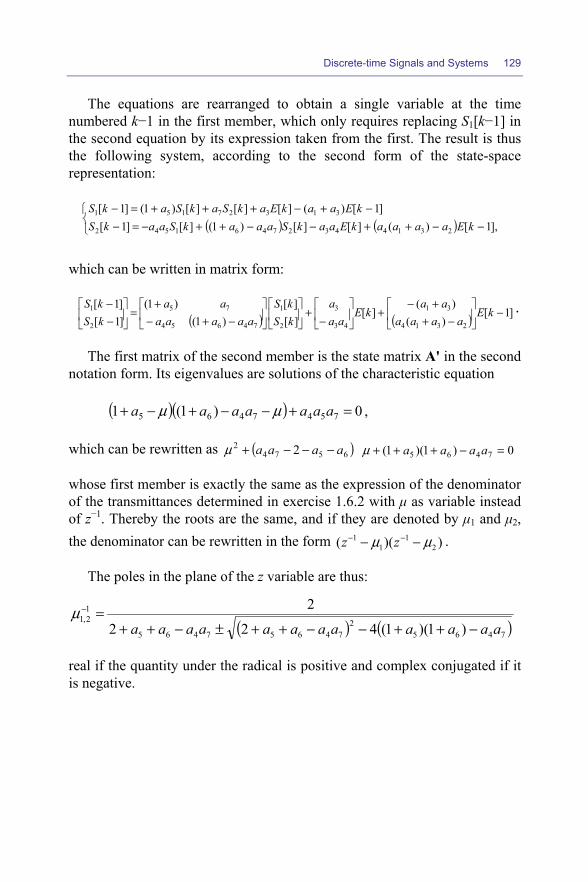
Discrete-time Signals and Systems 129
The equations are rearranged to obtain a single variable at the time numbered k−1 in the first member, which only requires replacing S1[k−1] in the second equation by its expression taken from the first. The result is thus the following system, according to the second form of the state-space representation:
( ) ( )
−−++−−++−=−−+−+++=−
],1[)(][][)1(][]1[]1[)(][][][)1(]1[
23144327461542
31327151
kEaaaakEaakSaaakSaakSkEaakEakSakSakS
which can be written in matrix form:
( ) ( ) ]1[)(
)(][
][][
)1()1(
]1[]1[
2314
31
43
3
2
1
74654
75
2
1 −
−+
+−+
−
+
−+−
+=
−−
kEaaaa
aakE
aaa
kSkS
aaaaaaa
kSkS .
The first matrix of the second member is the state matrix A' in the second notation form. Its eigenvalues are solutions of the characteristic equation
( )( ) 0)1(1 7547465 =+−−+−+ aaaaaaa μμ ,
which can be rewritten as ( )65742 2 aaaa −−−+μ 0)1)(1( 7465 =−+++ aaaaμ
whose first member is exactly the same as the expression of the denominator of the transmittances determined in exercise 1.6.2 with μ as variable instead of z−1. Thereby the roots are the same, and if they are denoted by μ1 and μ2, the denominator can be rewritten in the form ))(( 2
11
1 μμ −− −− zz .
The poles in the plane of the z variable are thus:
( ) ( )74652
74657465
12,1
)1)(1(4222
aaaaaaaaaaaa −++−−++±−++=−μ
real if the quantity under the radical is positive and complex conjugated if it is negative.
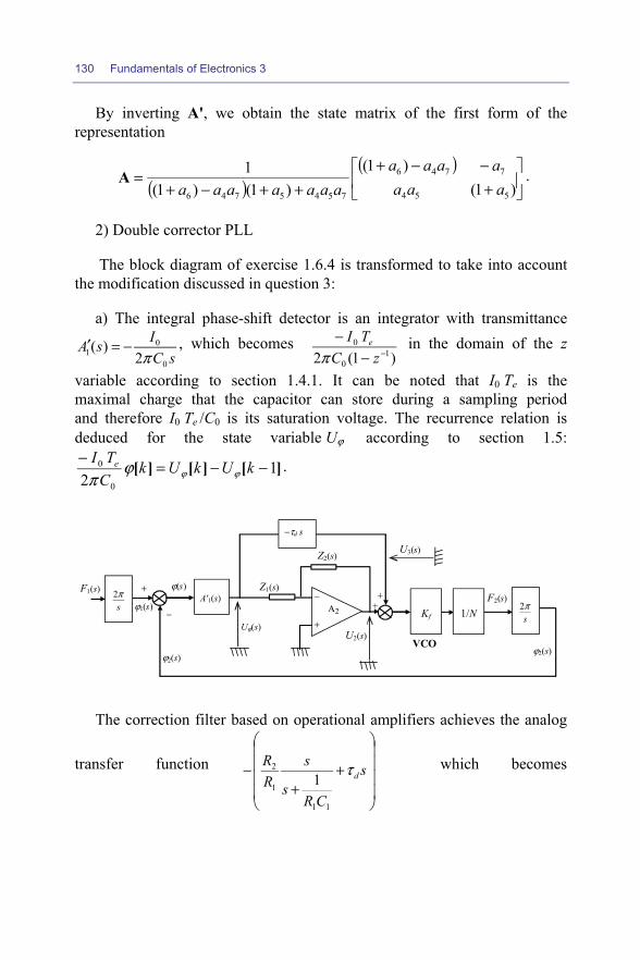
130 Fundamentals of Electronics 3
By inverting A', we obtain the state matrix of the first form of the representation
( )( )
+
−−+++−+
=)1(
)1()1()1(
1554
7746
7545746 aaaaaaa
aaaaaaaA .
2) Double corrector PLL
The block diagram of exercise 1.6.4 is transformed to take into account the modification discussed in question 3:
a) The integral phase-shift detector is an integrator with transmittance 0
10
( )2
IA sC sπ
′ = − , which becomes )1(2 1
0
0−−
−zC
TI e
π in the domain of the z
variable according to section 1.4.1. It can be noted that I0 Te is the maximal charge that the capacitor can store during a sampling period and therefore I0 Te /C0 is its saturation voltage. The recurrence relation is deduced for the state variable Uϕ according to section 1.5:
][][][ 12 0
0 −−=− kUkUkCTI e
ϕϕϕπ
.
Z1(s)
Z2(s)
Kf
F2(s)
Uϕ(s) U2(s)
A'1(s)
ϕ2(s)
−
+
sπ2
VCO
ϕ1(s)
ϕ2(s)
1/N
− Α2
+
ϕ(s) + +
−τd s
U3(s)
sπ2
F1(s)
The correction filter based on operational amplifiers achieves the analog
transfer function
++
− s
CRs
sRR
dτ
11
1
2
1 which becomes
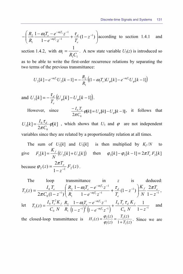
Discrete-time Signals and Systems 131
−+
−−−− −
−−
−−
)1(1
1 11
11
1
21
1
zTze
zeTRR
e
dT
Te
e
e τωω
ω
according to section 1.4.1 and
section 1.4.2, with 11
11CR
=ω . A new state variable U3(z) is introduced so
as to be able to write the first-order recurrence relations by separating the two terms of the previous transmittance:
( )]1[][)1(]1[][ 111
1
222 −−−−=−− −− kUekUT
RRkUekU ee T
eT
ϕω
ϕω ω
and ( )]1[][][3 −−−= kUkUT
kUe
dϕϕ
τ .
However, since ][][][ 12 0
0 −−=− kUkUkCTI e
ϕϕϕπ
, it follows that
][2
][0
03 k
CIkU d ϕπ
τ= , which shows that U3 and ϕ are not independent
variables since they are related by a proportionality relation at all times.
The sum of U2[k] and U3[k] is then multiplied by Kf /N to
give ( )][][][ 322 kUkUNK
kF f += then ][2]1[][ 222 kFTkk eπϕϕ =−−
because )(12
)( 212 zFzT
z e−−
=π
ϕ .
The loop transmittance in z is deduced:
11
1
11
1
21
0
03 1
2)1(1
1)1(2
)(1
1
−−
−−
−−
− −
−+
−−−
−=
zT
NK
zTze
zeTRR
zCTIzT ef
e
dT
Tee
e
e πτωπ ω
ω
,
let ( ) ( ) 1
0
0
121
11
1
2
0
20
3 11
111)(
1
1
−−−−
−−
−+
−−−−=
zNCKTI
zezzeT
RR
NCKTI
zT fde
T
Tefe
e
e τωω
ω
and
the closed-loop transmittance is )(1
)()()()(
3
3
1
23 zT
zTzzzH
+==
ϕϕ
. Since we are
132 Fundamentals of Electronics 3
looking for the transmittance )()(
1
2
zFzF where we have both
)(2
1)( 1
1
1 zTzzF
e
ϕπ
−−= and )(2
1)( 2
1
2 zTzzF
e
ϕπ
−−= , we also have:
)()()(
31
2 zHzFzF = .
b) The synthesis of the recurrence equations is carried out by employing the second form of the state-space representation and by replacing Uφ[k −1] by the second member of the first relation in the following:
][2
][]1[0
0 kCTIkUkU e ϕ
πϕϕ +=− (1)
+−−+=− ][
2][][)1(][]1[
0
0
1
21
1
222
11 kCTIkU
RRkUTe
RRkUekU e
eTT ee ϕ
πω ϕϕ
ωω (2)
Then by shifting from k to k −1, relation (3) is written:
where ϕ[k −1] will be replaced according to the state variables at time k at the end of the procedure and ][2][]1[ 222 kFTkk eπϕϕ −=− (4).
Finally, it is necessary to introduce the feedback loop and the subtractor, with ][][][ 21 kkk ϕϕϕ −= in which ϕ1[k] is an input variable. By shifting from k to k −1, the last equation is written as follows:
][2][]1[]1[ 221 kFTkkk eπϕϕϕ +−−=− (5).

Discrete-time Signals and Systems 133
We thus have in total five state variables: Uϕ, U2, F2, ϕ2 and ϕ.
The input variable ϕ1 depends on the other possible input variable F1
according to ( )]1[][2
1][ 111 −−= kkT
kFe
ϕϕπ
.
By replacing ϕ[k −1] in relation (3) by its expression taken from relation (5), the system can be written in matrix form and we can establish the expression of the state matrix A':
If F1 is the input variable, ϕ1[k −1] will be deduced from ][2][]1[ 111 kFTkk eπϕϕ −=− .
In this case,
−
−=
′=′][][
12002
0000
][][
1
1
0
0
0
0
1
10 k
kF
T
CI
NK
CTI
NK
kkF
e
dfdef
ϕ
π
πττ
ϕBB .
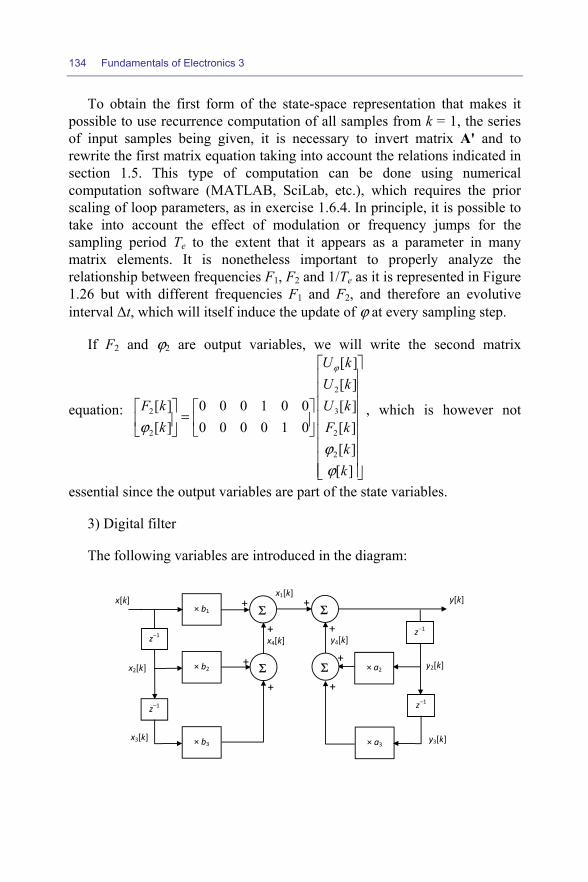
134 Fundamentals of Electronics 3
To obtain the first form of the state-space representation that makes it possible to use recurrence computation of all samples from k = 1, the series of input samples being given, it is necessary to invert matrix A' and to rewrite the first matrix equation taking into account the relations indicated in section 1.5. This type of computation can be done using numerical computation software (MATLAB, SciLab, etc.), which requires the prior scaling of loop parameters, as in exercise 1.6.4. In principle, it is possible to take into account the effect of modulation or frequency jumps for the sampling period Te to the extent that it appears as a parameter in many matrix elements. It is nonetheless important to properly analyze the relationship between frequencies F1, F2 and 1/Te as it is represented in Figure 1.26 but with different frequencies F1 and F2, and therefore an evolutive interval Δt, which will itself induce the update of ϕ at every sampling step.
If F2 and ϕ2 are output variables, we will write the second matrix
equation:
=
][][][][][][
010000001000
][][
2
2
3
2
2
2
kkkFkUkUkU
kkF
ϕϕ
ϕ
ϕ
, which is however not
essential since the output variables are part of the state variables.
3) Digital filter
The following variables are introduced in the diagram:
z−1
× b1 Σ+
+x1[k]
z−1
× b2
× b3
Σ+
+
z−1
Σ+
+
z−1
× a2
× a3
Σ+
+
y[k]
x4[k]
x2[k]
x3[k]
y2[k]
y3[k]
x[k]
y4[k]
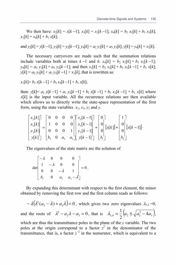
Discrete-time Signals and Systems 135
We then have: x2[k] = x[k −1]; x3[k] = x2[k −1]; x4[k] = b2 x2[k] + b3 x3[k]; x1[k] = x4[k] + b1 x[k];
and y2[k] = y[k −1]; y3[k] = y2[k −1]; y4[k] = a2 y2[k] + a3 y3[k]; y[k] = y4[k] + x1[k].
The necessary carryovers are made such that the summation relations include variables both at times k −1 and k: x4[k] = b2 x2[k] + b3 x2[k −1]; y4[k] = a2 y2[k] + a3 y2[k −1]; and then x1[k] = b2 x2[k] + b3 x2[k −1] + b1 x[k]; y[k] = a2 y2[k] + a3 y2[k −1] + x1[k], that is rewritten as:
x1[k]= b2 x[k −1] + b3 x2[k −1] + b1 x[k];
then: y[k]= a2 y[k −1] + a3 y2[k −1] + b2 x[k −1] + b3 x2[k −1] + b1 x[k] where x[k] is the input variable. All the recurrence relations are then available which allows us to directly write the state-space representation of the first form, using the state variables x2, x3, y2 and y.
[ ] [ ]]1[001
][000
]1[]1[]1[]1[
0100000010000
][][][][
21
2
3
2
233
2
3
2
−
+
+
−−−−
=
kx
b
kx
bkykykxkx
aabkykykxkx
.
The eigenvalues of the state matrix are the solution of
0
0100001000
det
233
=
−−
−−
λλ
λλ
aab
.
By expanding this determinant with respect to the first element, the minor obtained by removing the first row and the first column reads as follows:
( ) 0)( 322 =+−− λλλλ aa , which gives two zero eigenvalues λ1,2 =0,
and the roots of 0322 =−− aa λλ , that is ( )3
2224,3 4
21 aaa −±=λ ,
which are thus the transmittance poles in the plane of the z variable. The two poles at the origin correspond to a factor z2 in the denominator of the transmittance, that is, a factor z−2 in the numerator, which is equivalent to a
136 Fundamentals of Electronics 3
delay of two sampling periods in the discrete-time domain and which indicates that the result of the computation performed by the filter is obtained after this delay. In the expression of the poles which determine the denominator of the transmittance, only the multiplicative coefficients a2 and a3 which are included in the right-hand side of the diagram, are present. This is logical insofar as it is the only part of the diagram where recursivity is present due to the operations carried out on the output samples y[k]. There are two real poles in the plane of the variable z if 3
22 4aa > , and two complex
conjugated poles otherwise. These two poles induce a second-order behaviour. It is also logical that coefficients b1, b2 and b3 play no role in the pole expression of λ3,4 because they modify the input samples without recursivity, inducing a linear combination of the input samples x[k], x[k−1] and x[k−2] sent to the right part of the filter. For this reason, b1, b2 and b3 will appear only in the numerator of the transmittance, which does not influence the poles in any way.