digital guitar amplifier and effects · pdf filereverb ... this project hopes to put to rest...
TRANSCRIPT

Digital Guitar Amplifier and Effects Unit Shaun Caraway, Matt Evens, and Jan Nevarez
Group 5, Senior Design Spring 2014


i
Table of Contents
1. Executive Summary ....................................................................................... 1
2. Project Description ......................................................................................... 2 2.1. Project Motivation and Goals ................................................................... 2
2.2. Objectives ................................................................................................ 3
2.3. Project Requirements and Specifications ................................................ 3
3. Research ........................................................................................................ 4
3.1. Digital Signal Processing ......................................................................... 4
3.1.1. Requirements ................................................................................... 4
3.1.1.1. Sampling Rate ............................................................................... 4
3.1.1.2. Audio Word Size ............................................................................ 5
3.1.2. Processor Comparison ..................................................................... 5
3.1.3. Features ............................................................................................ 6
3.1.3.1. Programming Method .................................................................... 6
3.1.3.2. Real-Time OS ................................................................................ 6
3.1.3.3. Ports Available ............................................................................... 7
3.2. Analog ..................................................................................................... 7
3.2.1. Input .................................................................................................. 7
3.2.2. Output ............................................................................................... 8
3.3. Data Converts ......................................................................................... 9
3.3.1. Analog to Digital Converts ................................................................ 9
3.3.2. Digital to Analog Converts .............................................................. 10
3.4. Communication ..................................................................................... 11
3.4.1. UART .............................................................................................. 11
3.4.2. SPI .................................................................................................. 11
3.4.3. UPP ................................................................................................ 12
3.4.4. EMIF16 ........................................................................................... 12
3.4.5. SRIO ............................................................................................... 12
3.4.6. McBSP ............................................................................................ 13
3.5. Algorithms ............................................................................................. 13
3.5.1. K Method ........................................................................................ 14
3.5.2. Newton’s Method ............................................................................ 15
3.5.3. DK Method ...................................................................................... 16
3.5.4. DK Method Equations ..................................................................... 16

ii
3.5.5. Impedance Decomposition ............................................................. 17
3.5.6. Component Models ........................................................................ 18
3.5.7. Vacuum Tube Models ..................................................................... 18
3.5.8. Diode Model ................................................................................... 20
3.5.9. Transformer Model ......................................................................... 20
3.5.10. Effects Algorithms ....................................................................... 23
3.5.10.1. Delay ........................................................................................ 23
3.5.10.2. Reverb ..................................................................................... 24
3.5.10.3. Chorus ..................................................................................... 25
3.5.10.4. Compression ............................................................................ 26
3.5.10.5. Speaker Cabinet Simulation ..................................................... 27
3.6. Printed Circuit Board ............................................................................. 29
3.6.1. Layer Consideration ....................................................................... 29
3.6.2. OrCad ............................................................................................. 30
3.6.3. Eagle .............................................................................................. 30
3.6.4. Upverter .......................................................................................... 31
3.7. User Interface ........................................................................................ 31
3.7.1. On Board ........................................................................................ 31
3.7.1.1. On Board LCD ............................................................................. 31
3.7.1.2. Microcontroller for the LCD ......................................................... 32
3.7.1.3. Alternate Solution ........................................................................ 32
3.7.2. Computer ........................................................................................ 33
3.8. Power Supply ........................................................................................ 33
3.8.1. Linear Power Supply ...................................................................... 33
3.8.2. Switching Power Supply ................................................................. 34
3.8.3. Power Management ....................................................................... 35
4. Design ......................................................................................................... 37 4.1. Audio Inputs and Outputs ...................................................................... 37
4.1.1. Unbalanced to Balanced Signal ...................................................... 38
4.1.2. Headphone Output ......................................................................... 40
4.1.3. Stereo Output ................................................................................. 43
4.2. Data Convert Design ............................................................................. 44
4.2.1. Analog to Digital Converter ............................................................. 44
4.2.2. Digital to Analog Convert ................................................................ 48
4.2.3. Clocking .......................................................................................... 51

iii
4.3. Digital Signal Processor ........................................................................ 52
4.3.1. Clocking for Processor .................................................................... 52
4.3.2. Memory ........................................................................................... 55
4.3.3. Power On and Boot Sequence ....................................................... 56
4.3.4. Software .......................................................................................... 57
4.4. User Interface ........................................................................................ 59
4.4.1. Hardware Interface ......................................................................... 59
4.4.2. Software Interface ........................................................................... 61
4.4.2.1. Coding ......................................................................................... 62
4.4.2.2. Communication ............................................................................ 63
4.5. Printed Circuit Board Design ................................................................. 64
4.5.1. Printed Circuit Board Requirements ................................................ 65
4.5.2. Analog Board .................................................................................. 65
4.5.3. Digital Board ................................................................................... 65
4.5.3.1. Hardware configuration of the TMS320C6657 ............................. 66
4.5.3.2. Filtered Voltage Supplies ............................................................. 67
4.5.3.3. DDR3 Routing ............................................................................. 69
4.5.4. Bulk Power Supply Board ............................................................... 69
4.6. Power Supply Design ............................................................................ 70
4.6.1. Digital Sub System .......................................................................... 72
4.6.1.1. Power On and Off Sequencing .................................................... 75
4.6.2. User Interface Sub System ............................................................. 75
4.6.3. Input Output Sub System ................................................................ 75
4.6.4. Bulk Power Supply .......................................................................... 76
5. Design Summary ......................................................................................... 79
5.1. Hardware ............................................................................................... 79
5.2. Software ................................................................................................ 81
5.2.1. DSP ................................................................................................ 81
5.2.2. User Interface ................................................................................. 81
6. Prototyping ................................................................................................... 81 6.1. Software Algorithms Optimization ......................................................... 81
7. Project Testing ............................................................................................. 82
7.1. Hardware Specification Testing ............................................................. 82
7.1.1. Audio Input ...................................................................................... 82
7.1.2. Analog to Digital Converter ............................................................. 82

iv
7.1.3. Digital to Analog Converter ............................................................. 83
7.1.4. Audio Output ................................................................................... 83
7.1.5. Power Supply ................................................................................. 83
7.1.6. User Interface Hardware Testing .................................................... 85
7.2. Software Algorithm Testing ................................................................... 86
7.2.1. DSP ................................................................................................ 86
7.2.2. User Interface ................................................................................. 88
8. Administration .............................................................................................. 88
8.1. Milestone Discussion ............................................................................ 88
8.2. Budget and Finance Discussion ............................................................ 89
9. Appendix A – References ............................................................................... I 10. Appendix B – Permissions ............................................................................. II

v
Figure Listing Figure 1 Circuit Demonstration ........................................................................... 18 Figure 2 Triode Simulation ................................................................................. 19 Figure 3 Transformer Model ............................................................................... 21 Figure 4 Gyrator Model ....................................................................................... 23
Figure 5 Implementation of the Multi-Tap Delay ................................................. 24 Figure 6 Feedback Network................................................................................ 25 Figure 7 Cascade Network ................................................................................. 25 Figure 8 Chorus effect Simulation ...................................................................... 26 Figure 9 Transfer Function for Compressor ........................................................ 27
Figure 10 Speaker Cabinet Impulse Network ..................................................... 28 Figure 11 OPA827 Implementation Schematic ................................................... 39 Figure 12 Implementation of LT1028 as a Current to Voltage Convertor ........... 42
Figure 13 DRV 135 Line Drive Implementation Schematic ................................. 43 Figure 14 Frequency Response ADC at 48 kHz ................................................. 44 Figure 15 Frequency Response ADC at 96 kHz ................................................. 44
Figure 16 Bode Plot for High Pass Filter for PCM4222 ...................................... 45 Figure 17 McBSP Bock Diagram ........................................................................ 46 Figure 18 McBSP Data Converter ...................................................................... 47
Figure 19 Left-Justified format for the I2 S protocol ............................................ 47 Figure 20 Dynamic Range and THD + N ............................................................ 48
Figure 21 Signal to Noise Ration and Channel Separation ................................ 49 Figure 22 PCM1794A Block Diagram ................................................................. 49
Figure 23 System Clock Rates ........................................................................... 50 Figure 24 Connection Diagram ........................................................................... 51
Figure 25 Functional Block Diagram ................................................................... 52 Figure 26 LVDS Clock Output to CML Buffer ..................................................... 54 Figure 27 Amplifier Gain Stages ......................................................................... 58
Figure 28 User Interface Schematic ................................................................... 60 Figure 29 Menu Flow Chart ................................................................................ 62
Figure 30 User Interface Class Diagram ............................................................ 63 Figure 31 3-Pin SPI ............................................................................................ 63
Figure 32 Filter Circuit for Filtered Voltage Connection ...................................... 68 Figure 33 Texas Instruments SmartReflex Class 0 Power Supply for C6657 ..... 74 Figure 34 Bulk Power Supply Schematic ............................................................ 79 Figure 35 Spring Senior Design 1 Milestone ...................................................... 89 Figure 36 Summer Senior Design 2 Milestone ................................................... 89

vi
Table Listing Table 1 Processor Comparison ............................................................................ 6 Table 2 Line Level Standers for Professional and Consumer Grade Equipment . 9 Table 3 PCM3168A-Q1 Audio CODEC ................................................................ 9
Table 4 PCM4222 Audio A/D Converter ............................................................. 10 Table 5 PCM3168A-Q1 Specifications ............................................................... 10 Table 6 PCM1794A Specification ....................................................................... 11 Table 7 LCD Screen Comparison ...................................................................... 32 Table 8 Microcontroller Comparison................................................................... 32
Table 9 Power Supply Sequencing .................................................................... 37 Table 10 Texas Instruments OPA827 ................................................................ 40 Table 11 Texas Instruments TPA6120A2 High Fidelity Headphone Amplifier .... 41
Table 12 Comparison of TINE5534 and LT1028 Operational Amplifiers ............ 41 Table 13 Texas Instruments DRV 135 Audio Balanced Line Driver ................... 44 Table 14 Clock Inputs of C6657 ......................................................................... 53
Table 15 C6657 Clock Jitter Requirements ........................................................ 53 Table 16 C6657 Power on Sequence................................................................. 56 Table 17 C6657 Configuration Bits .................................................................... 57
Table 18 Pin Assignments of the MSP430G2553IPW28.................................... 61 Table 19 Bit Patter for SPI Communication ........................................................ 64
Table 20 Peripherals for the C6657.................................................................... 66 Table 21 C6657 Pin Connections for Filtered Voltage Supplies ......................... 68
Table 22 Device Power Requirements ............................................................... 71 Table 23 Power and Current Requirements for each Supply Voltage ................ 72
Table 24 Supply Voltage Regulators .................................................................. 72 Table 25 Power Characteristics of Regulators Utilized by C6657 ...................... 74 Table 26 Power Requirement for Source Regulators of the Bulk Power Supply 77
Table 27 Regulators Implemented on Bulk Power Supply ................................. 78 Table 28 Power Supply Test Loads ................................................................... 84
Table 29 Subsystems Voltage Regulators Max Voltage Ratings ....................... 85 Table 30 C6657 SPI Logic Voltages................................................................... 86
Table 31 Budget and Cost .................................................................................. 90

1
1. Executive Summary
Guitar amplifiers still utilize vacuum tubes as a means to amplify an electric guitar. Many musicians prefer the sound produced by a vacuum tube amplifier versus a transistor or digital implementation amplifier. When driven into a nonlinear state, vacuum tubes will distort in a gradual way that is pleasing to the ear. By contrast, when a transistor is saturated, it can tend to an overall harsh distortion that is not pleasing to the ear. The quality of the produced sound is the primary advantage of the vacuum tube amplifier over modern transistor amplifiers. However, vacuum tubes are relatively bulky, dissipate a large amount of heat, and are susceptible to becoming microphonic, where the vacuum tubes mechanically vibrate producing undesired sound. Their physical size when compared to transistors is a major disadvantage. The physical size of a guitar amplifier and complementary audio components is an area ripe for improvement. The speaker cabinet used for these amplifiers is large in size as well as the effects units that complement these amplifiers. The goal is to model and simulate the characteristics of these components in a digital environment in a compact form that allows portability and ease of use. By implementing everything in the digital domain, the user is afforded a more compact, portable solution to their overall system. The digital domain would also allow the user to obtain more amplifier, speaker, and effects modules than would previously be attainable due to size and lack of available capital. This project wishes to address these issues by creating a standalone device that would simulate vacuum tubes and the amplifiers that utilize them. Furthermore, the project will address a few other issues that arise from the use of these large amplifiers. The unit will also include the speaker cabinet simulations and digital effects that are normally used by musicians. This will reduce the overall cost that a musician would normally incur by investing in every component of a typical guitar rig and allow for far more flexibility than would normally be attainable in the analog domain. There are products that have similar capabilities as the proposed project. However, the available products are relatively expensive and are difficult to operate. Most of these products utilize a general purpose computer in order to run software for simulating such effects. The problem with this method is that it is a general purpose computer that has its resources divided and is not designed for manipulating floating point numbers at a high rate. Simulating a guitar amplifier circuit in real-time becomes a resource intensive task for the computer to handle. This design will utilize a separate DSP processor in order to simulate the amplifier circuit, speaker cabinet, and effects modules. It will need to run in real time and make the user feel as if they have just plugged their guitar into the amplifier that they have selected. The project will also include a more user-friendly interface than current products on the market by exploring new methods with which the user can interact with the device.

2
2. Project Description
2.1. Project Motivation and Goals
When you take a look around at current technology we see advances in many areas of electronics and computer software that were not possible ten years ago. The mindset is to make it smaller, faster, and better. That is the case for most areas of technology, at least for one area: guitar amplifiers. Still stuck in vacuum tube era, guitar amplifiers have not evolved like the rest of the world has. Still requiring a separate heater voltage and current, high plate voltages and large transformers, these devices are completely obsolete. So why are they still present in something such as a guitar amplifier? One reason is the nostalgia that is involved with these devices. Many of the individuals who grew up playing through a big, loud amplifier still prefer those amplifiers because of the way they sound when driven into saturation. There have been attempts to lure these individuals away from these large devices, but they always ended up staying with the vacuum tube amplifiers. Previous attempts failed due to poor design or extreme expense associated with the newer devices. This project hopes to put to rest that digital audio is “sterile” or “cold” sounding and create a new device that can effectively replace the devices of the past. The previous attempts failed not because solid state devices are incapable of reproducing the sound of the much sought after vacuum tube sound. They failed because the understanding of the newer and older devices were not present in order to accurately reproduce the pleasing sound of a vacuum tube in saturation. The goal of this project is to create a system for musicians that accurately replicates the sound of vacuum tube amplifiers, speaker cabinets, and effects units with great sound quality. A DSP algorithm is only as good as the surrounding circuitry that reproduces the sound. This project will be addressing all aspects of the signal path in order to ensure a high quality audio signal is reproduced from the beginning to the end. This entails proper design and high quality components where it is most critical. This project looks to replace the current systems that guitarist currently employ, which includes the amplifier, speaker cabinet, and effects unit. This is important because not only are the amplifiers themselves cumbersome, but so is the speaker cabinets necessary to reproduce the sound and any effects units that may be included in the system. Due to the nature of this project, it will be necessary to implement a powerful DSP in order to accurately replicate the typical system that a guitarist would use. This project also needs to make sure that the user can operate the device without much complication or the need for an overly complicated interface. Below is a diagram that shows the signal flow of the DSP based system.

3
2.2. Objectives
This audio digital guitar amplifier and effects unit will be the next big device for the music industry. The main objective, above all, for this project is to create a reliable, high performance unit with the capability of modeling vacuum tube amplifiers and a various range of guitar effects all in the digital world. This project will require a high performance digital signal processor to ensure the highest quality sound in an efficient amount of time. Since the normal human has the capability to notice a lag in sound from the time they play to the time they hear this project must be able to operate and model all amplifier and effects under this time frame. This project must also be portable since most music performers will be using our product in live concert event halls although it will still need to be plugged in to receive power. Also, we want to make sure that users can easily and readily use our product right after they open it out of the box by having an efficiency designed user interface for everybody to easily understand and use. This product will be able to simulate a range of different amplifier boxes made of vacuum tubes as well as effects unit all in a single unit and be attached to a speaker box to play or allow for headphones to play back all new modeled sounds.
2.3. Project Requirements and Specifications
The requirements and specifications in this section will be the guidelines for each subsequent design portion of this report. Each requirement and specification listed below will be further expanded upon in their respective sections.
The device will be a single self-contained unit. This includes user
interface, and power supply.
It will be powered by a wall outlet taking in 220-V at 60-Hz.
A bulk power supply will be used to create an 18-V DC supply voltage. DC
to DC regulation will then be used to power the TMS320C6657 processor,
Integrated circuits used for DAC and ADC, user interface and other
various features which will require a direct current source.
The device will simulate both vacuum tube amplifiers
The device will simulate 4 different guitar effects:
a. Delay
b. Reverb
c. Compression
d. Chorus
To prevent noticeable delay from input to output all processing of input
signals will be completed in no more than 3 milliseconds.
Electric Guitar Input
Guitar Amplifier Model
Speaker Cabinet Model
EffectsPA System and
Headphone Outputs

4
The device will take input from an electric guitar in the form of a 1/4 inch
mono jack (6.35 mm)
There will be several outputs on the device.
a. 1/8 inch (3.5mm) output for headphones.
b. 1/4 inch (6.35 mm) stereo output.
To interact with the device an integrated user interface will be provided.
This will consist of a LCD graphic module and a set of control nobs and
switches or possibly a LCD touch sensitive screen use to implement a
user graphical interface.
This project has been entered into the Taxes Instruments Innovation Challenge Design Contest. As a result of this the design will require the use of at least 3 different analog integrated circuits or 2 analog integrated circuits and 1 Texas Instrument processor. To meet these requirements the TMS320C6657 Fixed and Floating-Point Digital Signal Processor, MSP430 micro controller, and PCM4222 2-Channel 24 bit Analog to Digital Converter will be used in the design.
3. Research
3.1. Digital Signal Processing
3.1.1. Requirements
In this section we will discuss the requirements for the performance standards for the system. Our process must satisfy both the sound quality and time constraint from our requirements. These two requirements come from a range of different specifications that we must look into for choosing our process. Above those requirements we must make sure that the process is not only capable, but must also be cost effective, and have great accessibility. The specifications for our processor must include audio sampling rate, and audio word size.
3.1.1.1. Sampling Rate
For digital audio processing values are continuously sampled from an analog input single and are stored at certain intervals based of the sampling frequency of the system. Based off the Nyquist sampling theorem we must sample our signal at twice the highest frequency from our device. This will ensure that the signal will be perfectly reconstruction in the digital world for the best sound quality. The sound quality goes up because of the continuity of the reproduced signal. By increasing the sampling frequency the greatest continuity is ensured because the gaps between each stored values goes down. The only issue with a sampling frequency that is to high is the incapability of having a processor to be able to read each value and manipulate it to simulate our different amplifies and effects and send it back out before the next value comes in. For this we must choose a good medium for a frequency to ensure sound quality and time constraints. Since the average human ear has the capability of hearing bandwidths of 20 kHz with some humans being able to hear up to 23 kHz range. To be compliant with Nyquist theorem to sample for human hearing we must be around 44 kHz which is a common frequency band

5
for low grade audio systems. For our project we will be aiming for high grade performance so we will sample at 96 kHz.
3.1.1.2. Audio Word Size
The bit depth of an audio word determines the resolution of the signal being sampled, processed, and transmitted. The larger the bit depth then the greater the quality of the sample. This also varies directly with the signal-to-noise ratio of the output signal. Also the audio word contains quantization error which is the result of truncations of signal values performed when sampling and recording which compromises the signal integrity before it passes through the system. To reduce this error it is best to raise the number of bits to reduce the possibility for truncating audio words. The most commonly used audio word size is 16 bits which is used for compact discs. With 16 bit audio word size we can get a signal-to-noise ratio of about 96 decibels. For our project we will use an audio word size of 24 bits which will result in a signal-to-noise ratio of about 144 decibels.
3.1.2. Processor Comparison
For our digital guitar amplifier unit we looked at various processors and compared them on three different scales to see which would be best to use for our project. The three different metrics we used to compare the processors are frequency, memory space, and energy consumption. For this project we compared the BF537 Blackfin processor by Analog Devices, TMS320C6657 by Texas Instruments, and the TMS320C6457 also by Texas Instruments. The table, Table 1 Processor Comparison, below compares the frequency of the three processors. The frequency will tell us how fast each processor can execute each of the instructions. This metric is our top priority in picking our processor because the sampling rate we choose was 96 kHz. So while sampling at 96 kHz we need to make sure that we can process all our data before the next signal as well as to make sure our lag time is under 3 milliseconds. From the table below we can see that the TMS320C6657 is the best processor since it will run at a max frequency of 1250 MHz. The next metric we will compare is memory space. This is an import metric because with the more memory we have on board the less external memory we will need to add to program on. If we are able to not need any external memory this will speed up our overall unit because we will not need to worry about fetching instructions from memory which can be costly and could affect our ability to meet our time constraints. In Table 1 below we compare the onboard memory for each of the processors. For this comparison we can see there is not much difference between the Blackfin and TMS320C6657 processor. For the last metric we will use to compare processor is energy consumption. This metric will allow us to see how much over all power we will need to run not only the single processor but as the entire system. We would like to make the most cost effect machine possible so the less energy we consume the less we will need to

6
spend on the power supply. From Table 1 we can see that the Blackfin processor BF537 uses the least amount of watts.
Processor Frequency (MHz)
Memory Size (K Bytes
Energy (Watts)
BF537 600 132 0.78
TMS320C6657 1250 128 3.5
TMS320C6457 1200 64 1.57
Table 1 Processor Comparison After looking at all three of these metrics we decided that we will use the TMS320C6657 processor from Texas Instruments. This decision was made because the TMS320C6657 processor out performance the other two processor in speed. Since our biggest concern is timing this processor helps meet our requirements in being able to sample at a rate of 96 kHz and have less than a 3 millisecond lag time.
3.1.3. Features
3.1.3.1. Programming Method
The development of the signal processing applications for the TMS320C6657 process will take place on a PC. The PC will have Code Composer Studio (CCS) from Texas Instruments which will compile and debug all the code. For the development of our project we will use the TMDSEVM6657LS development board with integrated XDS200 emulator from EInfochips. This will allow us to code in Code Composer Studio and run in real time and debug our code. The development board for this project will be running SYS/BIOS Multicore Software Development Kit (MCSDK) from Texas instruments which will be explained more in the Real-Time OS section below. All the code will first be programmed in CCS on the PC and then ported over to the integrated XDS200 emulator through a USB to Serial port using Telnet client commination. This will allows us to interact and run all applications for debugging and test validation. All code for this project will be coded in the C language. For this project we will need simulate an amplifier with tubes which requires extensive math and matrix multiplication. To help with this the use of MATHLIB from Texas Instruments will help to ensure that all matrix multiplications will be done in the most timely and efficient manner.
3.1.3.2. Real-Time OS
The real-time Operating System (OS) we will use for our processor is the SYS/BIOS from Texas Instrument. This is a real-time scheduling and synchronization tool. This is important for us since our DPS processor has two cores to make sure that we are running all our code properly without having to code our own multithreading synchronization. This real-time OS also helps to minimize memory and CPU requirements whenever it can. For our real-time OS

7
we can either code in C or C++ through Code Composer Studios (CCS). We have chosen to do all of our coding for this project C. The real-time operating system is able to cut down on memory size because it modularize only the APIs you use and bound all into the executable program as well as eliminating object creation calls. This is good since we only have a limited amount of space on the processor for coding so it’s not important to import the entire MATHLIB library but the functions that we actual use and need. The real-time OS also structures support for communication and synchronization between threads with the use of semaphores. This will help us do multiple calculations at once that do not share critical sections and are able to run concurrently to help meet our time constraint for our project off less than 3 ms of lag time.
3.1.3.3. Ports Available
There are several ports available to use with the TMS320C6657 processor. The ports will allow us to interface with all of our external peripheral items. The most import thing is to make sure we can program our processor. We also will need to make sure we can communicate with both the analog to digital converter and digital to analog converter. The next item we will need to communicate with is the user interface. The last item we will have to interface with is external memory. The available ports we have to select from to access each of these different peripheral are: SRIO, PCIe, HyperLink, Gigabit Ethernet, 32-Bit DDR3, 16-Bit EMI, Universal Parallel Port (UPP), UART, McBSP, I2C, and SPI ports. Later in this section we will look at these ports in detail. Since the C6657 processor offers a range of different ports to interface with peripheral items each needs to be analyze to find the best possible to interface port to control the user interface, analog-to-digital convert. And the digital-to-analog converter.
3.2. Analog
3.2.1. Input
The input to the device will be an analog signal in the form of a small alternating current sent from an electric guitar. The guitar generates this signal through the use of a transducer that converts the mechanical vibrations of a guitar string into an alternating current. This is done through the use of a magnetic field generated by the pickups on the guitar. When a musician plays the guitar he or she causes the strings of the guitar to vibrate which in turn moves them within the magnetic field generated by the pickup. This disturbance of the field generates an alternating current which is sent from the guitar to an amplifier. To generate the magnetic field pickups employ two methods active, and passive the former being the most common. Active pickups use batteries to induce a magnetic field while passive versions use a ferrous material surrounded by a coil. There are several materials used in the design of the magnets for passive pickups ranging from ferrous steel to alloys. The most widely used material is an alloy of Aluminum Nickel and Cobalt known as Alnico. Not only does the magnetic material used vary but so does the design and shape of the magnetic core. Pickups commonly use either 6 magnetic pole pieces which are small cylinders, or a solid piece of marital known as a blade. Both of which have a coil of wire wrapped around them. Appling different

8
combinations of shapes and material have the ability to alter the sound of the guitar. Using pole pieces of Alnico alloy reportedly generates brighter tighter tones, while their steel counterparts produce a loose fatter tone. Originally pickups were a single coil wrapped around the magnetic material. These early pickups were very susceptible to interference generated by other electronic device and prone to unwanted feedback. However in 1955 Seth Lover ¬an engineer working for Gibson Musical instruments invented a two coil pickup. This two coil pickup became known as the Humbucker, for its ability to remove unwanted hum from the output of the guitar. The Humbucker works by using two coils which are 180 degrees out of phase of each other. This effectively subtracts an unwanted signal such as noise from each other canceling them out. When designing the analog input to the Digital Guitar Amplifier and Effects Unit there are several things that will be considered. To avoid signal degradation and allow for the greatest maximum voltage to be transmitted from the guitar to the device the input impedance of the device will need to be much greater than that of the guitars output. Traditionally guitars featuring active pickups have very low output impedances generally 100-ohms. While guitars featuring passive pickups have higher output impedances ranging from 6k to 10k-ohms. The device will be designed to receive input from an electric guitar via a 1/4 inch mono jack (6.35 mm) however guitars are not the only device that uses this type of jack. Special considerations in the form of over voltage protection may be implemented to protect the device. This would assure that if an active device sourcing more voltage than the input can handle it will not be damaged. When dealing with audio signals noise always needs to be taken into consideration. To help combat unwanted noise the input signal will be converted from an unbalanced signal to a balanced one allowing for common mode rejection to filter noise that may be introduced throughout the processing of the signal within the device.
3.2.2. Output
The device will be designed to output an analog signal to headphones via a 3.5mm output jack, and audio mixing tables, independently powered speakers such as a public address system via a ¼ inch (6.35mm). There is a large range of headphones commonly availed on the market which utilizing some form of transducer to create an audible sound from an input signal. The most commonly used transducers in headphones are moving coils and electrostatics. Headphones featuring the electrostatic transducers require a large voltage input ranging from 100-V to 1000-V, can have input impedances reaching up to 170-Kohms, and can easily cost thousands of dollars. Less costly headphones employ mechanical transducers called moving coil drivers. Headphones ranging from cheap 5 dollar ear buds to more expensive 200 dollar consumer grade headphones. The input impedances of these headphones can be as low as 16-ohms. The device will be designed to provide appropriate output for headphones ranging in input impedances of 16 to 60 ohms. This will allow for low cost and consumer grade headphones to be utilized with the device. To interface the headphones with the device a 3.5mm jack will be made available. The device will also feature a volume

9
control for both the stereo and headphone outputs via the user interface. The volume will be adjusted digitally while the signal is being processed by C6657 DSP chip. The device will provide two channel differential stereo output at line level. Line level is an industry standard for connecting analog audio devices including but not limited to mixing tables, and audio amplifiers. Line level industry standers for professional and consumer grade equipment are listed in the following Table 2
Peak Amplitude
Peak to Peak Amplitude
Nominal Level
Nominal Level
Professional 1.736 V 3.472 v 1.228 Vrms +4 dBu
consumer 0.447 V 0.894 v 0.316 Vrms −10 dBV
Table 2 Line Level Standers for Professional and Consumer Grade Equipment Typically the output impedance of audio equipment souring an output at line level ranges from 100 to 600-ohms. While inputs for line level connections feature input impedances greater than 10000 -ohms. The devices output will designed to source a stereo output at a line level capable of interfacing with professional grade equipment. The output impedance of the device will also be designed to fall within the range of 100 to 600 ohms to allow for the maximum voltage transfer to other equipment featuring much larger input impedances.
3.3. Data Converts
3.3.1. Analog to Digital Converts
In order to process the incoming guitar signal it will need to be converted to a digital signal. The analog to digital converters will play an important role in the integrity of the overall signal that will be processed. The project will implement high quality converters in order to ensure that the guitar signal coming in is represented with minimal distortion. Due to the desire to have the upmost quality and since there are no real restrictions on overall power draw an audio CODEC will not be implemented in this design. Although CODECs provide a convenient package with low power draw, they do not meet the desired specifications for this project. Below are two tables that compares the very best audio CODEC that TI offers with the very best audio A/D converter that TI offers. Table 3 shows some specifications for the PCM3168A-Q1 audio CODEC (A/D converter). Table 4 shows some specifications for the PCM4222 audio A/D converter.
SNR 107 dB (differential)
THD+N -93 dB (differential)
Channels 6
Audio Formats PCM (Right-Justified, Left-Justified,
𝐈𝟐𝐂, and TDM)
Table 3 PCM3168A-Q1 Audio CODEC

10
SNR 122 dB
THD+N -108 dB
Channels 2
Audio Formats PCM (Right-Justified, Left-Justified,
I2C, and TDM)
Table 4 PCM4222 Audio A/D Converter It can be seen that the PCM4222 has better overall dynamic range and SNR. Although the PCM3168A-Q1 has more available channels, this project will only need one channel for the A/D conversion. Both converters output a PCM signal, which will be sent to the DSP as a Left-Justified signal. The PCM4222 is also a hardware controllable device which allows for the use of basic logic switches to control the sampling frequency, HPF, etc. For this project, since the sampling frequency and the mode of operation are going to be static, hardware implementation is all that is required as the need for software control will not be necessary and thus another microcontroller will not be needed.
3.3.2. Digital to Analog Converts
The digital to analog converters for this design play just as much of an important role as the analog to digital converters. The requirements for the digital to analog converters will be to the same standards as to the analog to digital converters. Once again by comparing the PCM3168A-Q1 to a standalone digital to analog converter, there exists a wide disparity in performance. The PCM1794A from Texas Instruments provides excellent performance in a hardware controllable package. The design will require the need for two of these devices due to the fact that there will be a standard stereo output at line level and a headphone amplifier. Both the headphone amplifier and stereo line driver require two channels of fully differential amplification. The main reason for needing two of these devices is there is a desire to control the volume of the headphone amplifier. The stereo line driver will not need to be controlled as the line out standard dictates that 1.228 VRMS be the maximum present signal. In Table 5 and Table 6 show some specifications for the PCM3168A-Q1 and PCM1794A respectively.
SNR 112 dB
THD+N -94 dB
Channels 8
Audio Formats PCM (Right-Justified, Left-Justified,
I2C, and TDM)
Table 5 PCM3168A-Q1 Specifications

11
SNR 127 dB (2V RMS, Stereo)
THD+N 0.0004%
Channels 2
Audio Formats PCM (Right-Justified, Left-Justified,
I2C, and TDM)
Table 6 PCM1794A Specification It can be seen that the PCM1794A has superior performance when compared to the PCM3168A-Q1 (D/A converter). Although there are advantages to using an audio CODEC with respect to power consumption and controllability, the performance required for this design is not adequate enough. Using separate analog to digital and digital to analog components with their own dedicated external clock will provide the best available performance and thus will offer better overall sonic characteristics.
3.4. Communication
3.4.1. UART
The Universal Asynchronous Receiver/Transmitter (UART) peripheral on the TMS320C6657 is a communication port that uses the industry standard TL16C550. This port allows for serial-to-parallel conversion of data to the CPU which will be used to program our processor. The processor can read the UART status at any time as well as be interrupt with the control capability from the UART port. The UART port also allows for a programmable baud which is capable to divide the input clock by divisors from 1 to 65535. The UART on the TMS320C6657 processor also has additional features listed below that might be helpful:
Choice of 1.8V, 2.5v, 3.3V, or 5V supply
Single, dual, and quad channel devices available
Transmit and receive FIFOs of either 16 or 64 Byte depth
Programmable sleep mode and low-power mode
3.4.2. SPI
The Serial Peripheral Interface (SPI) port on the TMS320C6657 processor is used for high-speed synchronous serial port for input and output bit streaming of lengths 2 to 16 bits. This is done by shifting in and out of the device at a pogrommed bit-transfer rate. We can use the SPI peripheral to interface with external I/O or other support compatible devices. This will be useful to us if we would want to control our analog-to-digital converters or an external microcontroller for controlling the user interface. The SPI port on the TMS320C6657 also has additional features listed below that might be helpful:
16-bit shift register
Slave in, master out I/O pin
Slave out, master in I/O pin
Multiple slave chip select I/O pins
Programmable SPI clock frequency range
Programmable Character length (2 to 16 bits)

12
Interrupt capability
Integrated DMA controller
Up to 66 MHz operation
3.4.3. UPP
The Universal Parallel Port (uPP) peripheral on the TMS320C6657 processor is used for high-speed parallel interface that has dedicated data lines but minimal control signals. We can use this design to interface with high speed analog-to-digital converters or digital-to-analog converters. This would be good to help with the speed to make sure we cut down time it takes to convert all our signals to allow for more time to analyze and compute our simulation of amplifiers and effects to meet our time constraint for out project. The uPP peripheral also includes an internal DMA controller to help maximize its throughput and help minimizes the overhead to the CPU. We could also use the uPP port to interface with a field-programmable gate array (FPGA) that could be used to help maintain the proper power to the entire system. The uPP port on the TMS320C6657 also has additional features list below that might be helpful:
Two independent channels with separate data buses
Channels can operate in same op opposing directions simultaneously
I/O speeds up to 75 MHz
8-16 bit data width per channel
Internal DMA
Single and double data rates
Data interleave mode
3.4.4. EMIF16
The External Memory Interface peripheral on the TMS320C6657 processor which utilizes a 16 bit bus (EMIF16). This bus will be used to interface with all sorts of asynchronous memory devices. The EMIF16 can accesses a total of 256 Mbytes of memory by using four chip selects with each at 64 Mbytes per chip select. This port will allow to for devices like ASRAM, NOR, and NAND memory to be accessed. Unfortunately there are several synchronous memories that the EMIF16 does not support which are DDR1, SDRAM, SDR, and Mobile SDR. This peripheral port ton the C6657 processor will allow for the unit to access more memory since the memory on the processor is very limited. The EMIF16 port also has additional features listed below that might be helpful:
8-bit and 16-bit data widths
Programmable cycle timings for each chip select
Extended wait support
Select strobe mode
Page/Burst mode read support for NOR flash
Big and little endian operation
3.4.5. SRIO
The Serial Rapid IO (SRIO) peripheral on the TMS320C6657 processor allows for non-proprietary, high-bandwidth, system-level interconnect. It is a packet-switched

13
interconnect intended primarily as an intrasystem interface for chip-to-chip and board-to-board communications at gigabyte-per-second performance levels. Uses for this architecture can be found to connect microprocessors memory, and memory-mapped I/O devices that operate in networking equipment, memory subsystem, and general-purpose computing. The SRIO line rates supported by the C6657 process device are 1250 Mbps, 2500, Mbps, 3125 Mbps, and 5000 Mbps. The rate scale is used to translate the output of the SRIO PLL to the line rate using the following formula: Line rate Mbps = PLL Output/rate scale. The SRIO port on the C6657 processor also has additional features listed below that might be helpful:
Flexible system architecture that allows peer-to-peer communication
Robust communication with error-detections features
Frequency and port-width scalability
Operation that is not software intensive
High-bandwidth interconnect with low overhead
Low pin count
Low power
Low Latency
3.4.6. McBSP
The multichannel buffered serial port (McBSP) allows for a direct interface with other Texas Instruments DSPs, codecs, or other devices in system. Since the device will be transmitting and convert audio signals this ports primary use is for audio interface. The two primary audio modes that are supported by the McBSP are the AC97 and the IIS modes. This port may also be used and programmed to support other serial formats but Texas Instrument documentation on the McBSP suggest not if a high-speed interface is needed. The McBSP uses a 32-bit-wide control registers which can be accessible via the internal peripheral bus. This port allows for a data path and a control path to connect external devices. This port will be best used for a project to connect the analog-to-digital converter and the digital-to-analog converters to the C6657 processor. Additional features of the McBSP port that may be helpful are:
Full-duplex communication
Double-buffered data register for continuous data stream
Independent framing and clocking for receive and transmit
Direct interface to industry-standard codecs
External shift clock or an internal, programmable frequency shift clock for data transfer
3.5. Algorithms
In order to properly simulate a guitar amplifier, the circuit of the amplifier will need to be simulated in order to ensure that the characteristics of the amplifier are properly captured and replicated. There have been many advances in the area of real-time simulation for non-linear systems of differential equations. Our project intends to use the most recent advances in order to ensure that our models are accurate and able to run in real-time. The goal of the simulations is not to capture the exact sound of the amplifier being simulated, but to capture the characteristics

14
and response of every amplifier. The simulations will include the simulation of the power supply, preamplifier, tone stack, and power amplifier circuits. We will ignore the parasitic components that are inherent in passive components as well as layout parasitic such as PCB inductance, resistance, and capacitance. However, parasitic components of active devices and transformer models will be included as these have a far greater effect on the response of the amplifier than the passive and PCB parasitic.
3.5.1. K Method
Due to the fact that the simulation of active devices (specifically vacuum tubes) are inherently non-linear, we are forced to deviate from the traditional state space representation methods typically used to represent this system. Instead we will adopt the DK method developed by David Yeh in order to simulate a non-linear, differential system. The DK method is an automated process that allows us to quickly construct and solve the non-linear differential equations. The derivation is constructed from the K-method which will need to be reviewed before going to the DK method. The equations that describe the K method are below.
= Ax + Bu + Ci
Equation 1
i = f(v)
Equation 2
v = Dx + Eu +Fi
Equation 3 Where x is the state of the vector being represented in the system, u is the input, and i is the non-linear function which is a function of v. The non-linear function usually results in an implicit equation and it is necessary to use Newton’s Method for solving the implicit equations. In order to approximate the system, the trapezoidal rule is implemented in the form of the Bilinear Transform to solve the system in the discrete time domain. The discretized state update equation using the Bilinear Transform becomes.
xn = H(αI + A)xn−1 + HB(un + un−1) + HC(in + in−1)
Equation 4
Where = (∝ 𝐼 − 𝐴)−1 , I is the identity matrix with the dimensions of A and α = 2/T. The variable v becomes.
𝑣𝑛 = 𝐷𝐻((𝛼𝐼 + 𝐴)𝑥𝑛−1 + 𝐵(𝑢𝑛 + 𝑢𝑛−1) + 𝐶𝑖𝑛−1) + 𝐸𝑢𝑛 + (𝐷𝐻𝐶 + 𝐹)𝑖𝑛
Equation 5

15
The function vn can be broken up into two terms. One that includes a linear parameter and the other contains the non-linear parameter. They can be represented by the following equations.
𝑝𝑛 = 𝐷𝐻((𝛼𝐼 + 𝐴)𝑥𝑛−1 + 𝐵(𝑢𝑛 + 𝑢𝑛−1) + 𝐶𝑖𝑛−1) + 𝐸𝑢𝑛
Equation 6
K = DHC + F
Equation 7 This results in the implicit function for the non-linear function below
in = f(pn + Kin)
Equation 8
The procedure for solving the system involves solving for 𝑝𝑛, in, then update xn. After those variables have been solved for the output can be determined based on the system in the general form below.
y = A0x + B0u + C0i
Equation 9
Where 𝐴0, 𝐵0, 𝐶0 are the coefficient matrices for the output.
3.5.2. Newton’s Method
In order to solve for the implicit equation that exists in in, Newton’s method is necessary to solve the system of equations. It was found by Yeh that iterating on voltages results in faster convergence of the solution. It was also found that the use of homotopy is necessary to ensure convergence for large signals (similar to those that will be found in our simulations). The procedure for solving using Newton’s method is below.
v = Dx + Eu + Ff(v)
Equation 10
vn = pn + Kf(vn)
Equation 11
f(vit) = −vit + pn + Kf(vn)
Equation 12
Taking the Jacobian of the function vn we get.
J(vit) = KJF(vit) − I
Equation 13

16
We finally arrive at the final Newton’s method equation for solving the voltages of the non-linear functions below.
vit+1 = vit − J(vit)−1f(vit)
Equation 14 Homotopy will need to be used to ensure that the initial guess of the system is close enough so that Newton’s method converges. Homotopy works by creating a new parameter in the equation in order to create a continuous path from the point where the parameter is equal to zero and when the parameter is equal to one. Below is a general form of homotopy used in conjunction with Newton’s method. The initial guess of the system is denoted as x* = 0.
𝐻(𝑥, 𝛼) = 𝐹(𝑥) + (𝛼 − 1)𝐹(𝑥∗) = 0
Equation 15 It will be decided during testing if the use of look-up tables for the non-linear functions is a better choice without losing accuracy and taking up too many resources.
3.5.3. DK Method
Although the K method provides an accurate means for deriving the necessary filters for the simulations, there is not an automated way of creating the equations without rigorous mathematical derivations. David Yeh proposed a method in his thesis that would help automate the process to speed up derivations and to create a more general form of the K method. The method takes advantage of the Modified Nodal Analysis (MNA) in order to create conductance, current source, and voltage node vectors to aid in the derivation. In order to avoid singular matrices, each energy storage component must be constructed into discrete companion circuits. Once this occurs than one can proceed and construct the matrices in order to solve the entire system.
3.5.4. DK Method Equations
The DK method will utilize Modified Nodal Analysis in order to build the system of equations for the simulation. The equation below represents the general form of the system to be solved.
Mx (t) = f(t, x, u)
Equation 16 The matrix M will be our conductance vector G, I will be the current source vector, and V is the node voltages and unknown currents. In order to avoid a singular solution in the M matrix, a component wise discretization of energy storage elements must be done. The trapezoidal rule is chosen in order to approximate these elements. This will result in a general form for capacitors and inductors below.

17
𝑥[𝑛] = 𝑍(2𝐺𝑣[𝑛] − 𝑥[𝑛 − 1])
Equation 17
Where 𝐺 = 2𝐶
𝑇, Z = 1 for the capacitor and 𝐺 =
𝑇
2𝐿, Z = -1 for the inductor. The state
is represented by x and v[n] is the voltage across the element. By using the same procedure with the K method we arrive at a general form for the state update equation and Newton’s Method equations as shown below.
v[n] = Ax[n − 1] + Bu[n] + Ci(v[n])
Equation 18
p[n] = Dx[n − 1] + E[u]
Equation 19
f(vit) = −vit + pn + Ff(vn)
Equation 20
J(vit) = KJF(vit) − I
Equation 21
vit+1 = vit − J(vit)−1f(vit)
Equation 22
A = GAe + S, B = GBe, C = GCe, where 𝐴𝑒 = 𝑀−1𝑀1, 𝐵𝑒 = 𝑀−1𝑀2, 𝐶𝑒 = 𝑀−1𝑀3 . The procedure remains the same as the K method with respect to solving for the non-linear, implicit equations.
3.5.5. Impedance Decomposition
One of the drawbacks to using a method such as the DK method or K method is the inherently large matrices that will be constructed in order to simulate the circuits. One method would be to take each stage in a circuit and break it up into blocks to reduce matrix dimensions resulting in faster algorithms. The main drawback of this method is that there is not a clear cut way to accurately simulate the loading affect that each stage would have on previous circuits. Other methods exist for simulating guitar amplifiers, but are either inefficient or focus solely on feed forward circuits. For this project, we propose a method in order to accurately simulate the loading between each stage in order to simplify our matrix dimensions. The Impedance decomposition method takes a stage in any given circuit, say the RC circuit in fig. 1, and adds an arbitrary impedance Z_L in parallel with the circuit. This will serve as a place holding impedance that represents the input impedance of the connecting circuit. Only one more equation is needed in order to represent the input impedance of the connecting circuit. In the case of the vacuum tube amplifier

18
circuit in Figure 1 Circuit Demonstration, if another amplifier circuit is connected to the previous amplifier circuit, there exists an instance where there many become an indefinite solution. In this case the user will simply create a special case for the instance of an indefinite solution and continue with the previously derived formula for the input impedance of the connecting circuit. By decomposing the circuits this way, it can be seen that the entire system can be simplified in order to improve matrix operation speeds within the DSP. The only drawback to this method is that it will require the input impedance to be calculated before each state update, but this is more than a fair trade off considering the reduction of matrix dimensions
Figure 1 Circuit Demonstration
3.5.6. Component Models
In order to successfully model an electronic circuit we need to understand the mathematical models for each component. For our passive components we will be taking the ideal component model for a resistor, capacitor, and inductor. Although these components have parasitic components to them, their effect on the entire system response is minimal and we will ignore these for our project. For active devices, we will consider the majority of these parasitic capacitances and inductances as these do have a considerable effect on the system response. We will look at models for the vacuum tubes, diodes and transformers that exist in a common guitar amplifier.
3.5.7. Vacuum Tube Models
The vacuum tubes that will be modelled in our simulations include the 12ax7a, EL84, EL34, and 6L6GC. These are four of the most common models that can be found in many commercially available guitar amplifiers. We will ignore the effect that the heater circuit has on the active devices, as their only contribution is in the

19
noise floor. For a triode such as the 12ax7a, the equation below developed by Marco Re Cardarilli will be used to simulate the triode.
is = G((Vgc)(Vgc +Vac
μ(Vgc, Vac)+ h(Vgc))
32
Equation 23
ig =is
1 + DVac
Vgc
K
Equation 24
ia = is − ig =
G((Vgc)(Vgc +Vac
μ(Vgc)+ h(Vgc))
32
1 +1
DVac
Vgc
K
Equation 25
Where 𝐺 = ∑ 𝑎𝑖𝑉𝑔𝑐𝑖3
𝑖=0 μ = ∑ 𝑏𝑖𝑉𝑔𝑐𝑖3
𝑖=0 h = ∑ 𝑐𝑖𝑉𝑔𝑐𝑖3
𝑖=0
The coefficients ai, bi, and ci are determined through curve fitting of the datasheet to get the best fit. Figure 2 shows the large signal model that will be used for the triode simulation.
Figure 2 Triode Simulation
For the pentode models, which include the 6L6GC, EL34, and EL84 we will be using Koren’s vacuum tube model, which is shown in the equations below. The grid current for the pentode can be expressed by the equation below derived by Cohen.

20
Ia = E1Ex(1 + sgn(E1)) arctan (Uak
Kvb)
Equation 26
𝐸1 =𝑈𝑔2𝑘
𝐾𝑝log (1 + exp (𝐾𝑝 (
1
𝜇+
𝑈𝑔1𝑘
𝑈𝑔2𝑘))
Equation 27
𝐼𝑠 =exp (𝐸𝑥log (
𝑈𝑔2𝑘
𝜇 + 𝑈𝑔1𝑘)
𝐾𝑔2
Equation 28
𝐼𝑔 = 𝑔𝑐𝑓(𝑉𝑔𝑘 − 𝑔𝑐𝑜)32, 𝑉𝑔𝑘 ≥ 𝑔𝑐𝑜
0, 𝑉𝑔𝑘 < 𝑔𝑐𝑜
Equation 29
Where gcf = 1 ∙ 10−5 and gco = −0.2.
3.5.8. Diode Model
For the simulation of the power supply diodes we will use the standard diode equations below.
𝑖𝐷 = 𝑖𝑠(exp (𝑣𝐷
𝑛𝑣𝑡) − 1)
Equation 30
Where 𝑣𝐷 is the voltage across the diode, n is the ideality coefficient, and 𝑣𝑡 is the thermal voltage which is about 26mV at room temperature. The diode will model will be necessary for accurate power supply simulation, specifically when simulating ripple voltage across each vacuum tube device. There are also distortion circuits that may become present in some amplifier models that utilize a diode clamping circuit to create distortion in between vacuum tube stages.
3.5.9. Transformer Model
There are a couple of models for the output transformer model that will be considered for the simulation. Below is the ideal transformer model that assumes the linear operating region and no loses due to hysteresis, core saturation, parasitic capacitances, parasitic inductances, and resistances of the windings in the transformer.

21
Vs
Vp=
Ns
Np=
ip
is
Equation 31 Although this model will give accurate response for the ideal situation while operating in the linear region, the objective of the simulation is to give the most accurate simulation possible to accurately replicate the distortion typically found in guitar amplifiers. Figure 3 shows the transformer model with the parasitic components of the winding, core hysteresis, and core saturation.
Figure 3 Transformer Model
The model in Figure 3 allows the transformer model to be broken up into an electrical and magnetic model. The resistors, capacitors, and inductors can be considered a part of the circuit model instead of the transformer model. The magnetic core also needs to be modeled in order to accurately model a non-ideal, non-linear transformer. The equation below represents the typical relationship in the magnetic core of the transformer.
B = μH
Equation 32 There exists three common models that the magnetic core can be represented as, the Frohlich model and the Jiles-Atherton (JA) model. The Frohlich model can be expressed as:
B =H
c + b|H|
Equation 33 Where c and b are the parameters that are derived from the material that makes up the transformer core. The JA model can be expressed as
B = μ0(M + H)
Equation 34 Where M is can be derived from the expression:

22
dH
dM= δM
Man − M
ksign (
dH
dt) + c
dMan
dH
Equation 35
𝑀𝑎𝑛 = 𝑀𝑠 (𝑐𝑜𝑡ℎ (𝐻 + 𝛼𝑀
𝑎) −
𝑎
𝐻 + 𝛼𝑀)
Equation 36
Where 𝑀𝑎𝑛, α, a, c, and k are derived from the material properties of the transformer core. When the nonphysical minor loop is going to be generated then
δM = 0 and when the nonphysical minor loop is not going to be generated δM = 1. The Frohlich model has the advantage of being fairly accurate and less computationally complex. The JA model although is the more accurate model is more robust in terms of computational complexity. This means that the JA model may not be suitable for real-time operation, although the models will be compared during testing procedures to verify if the model is too complex. The final model to consider is the gyrator-capacitor model. This model is based on a non-linear capacitor and non-linear resistor. The non-linear capacitor can be expressed as a constant capacitance C in series with a voltage controlled voltage source expressed as:
v(vc) = |avc|nsign(vR)
Equation 37
Where 𝑣𝑐 is the controlling voltage over the constant capacitor and A and N are saturation parameters. The non-linear resistor is implemented as a constant resistor R connected in parallel with the voltage controlled current source which can be expressed as:
i(vR) = |bvR
R|
n
sign(vR)
Where 𝑣𝑅 is the controlling voltage over the constant resistor an b and m are the hysteresis parameters. The main advantage that the gyrator-capacitor has over the Frohlich model is the gyrator-capacitor model will model the hysteresis loop, where the Frohlich model does not model the hysteresis loop. The advantage over the JA model is that the gyrator-capacitor model is more computationally efficient while maintaining good accuracy. The JA model is still more accurate but as stated before requires more computational complexity and could potentially be too robust for real-time simulation. Figure 4 illustrates the equivalent circuit model of the gyrator model.

23
Figure 4 Gyrator Model
3.5.10. Effects Algorithms
For guitarist effects are a very integral portion to the sound of the guitar. There are a few common effects that will be modeled which include, delay, reverb, compression, and chorus. Each algorithm will be covered in detail in order to gain a better understanding of what each effect is supposed to do. For this project the complexity of the algorithms will be kept to a minimum as the main purpose is to demonstrate the convenience that the final prototype will have. A finished product would implement slightly more refined and advanced effects. Since the main focus is on the accuracy of the amplifier algorithms and the fact that there are many advanced algorithms implemented in many other products he focus will be to implement simple effects. Although the distortion from the guitar amplifier is technically an effect, this will not be included in this section as the distortion is part of the amplifier circuit.
3.5.10.1. Delay
The delay effect is a commonly used effect not just guitars, but also for many other sources including percussion, vocals, etc. The basis of the effect is to delay the incoming signal at a certain frequency and sum the processed audio back into the original signal to create the effect of the source being in a large hall or room. Although there exist many types of delays, this design will focus on the multi-tap delay. One way to implement a multi-tap delay is to implement two delay lines and using feedback to create more reflections. Figure 5 shows the system implementation of the multi-tap delay.

24
Figure 5 Implementation of the Multi-Tap Delay
Changing the delay values will affect the frequency of the delay effect. In Equation 38 is the effect represented in the Z domain.
𝐻(𝑧) = 𝑏0 + 𝑏1 (𝑍−𝐷1
1 − 𝑎1𝑍−𝐷1) + 𝑏2 (
𝑍−𝐷1
1 − 𝑎1𝑍−𝐷1) (
𝑍−𝐷2
1 − 𝑎2𝑍−𝐷2)
Equation 38
3.5.10.2. Reverb
Reverb is another common effect used for guitars to simulate the guitar amplifier being in a large acoustic space. The difference between delay and reverb lies mostly in the complexity and in the design of the delay to produce the effect. Reverb consist of three main components which include the direct sound, early reflections, and late reflections. The reverb that will be implemented in this design will be an algorithm that was designed by M.A Schroeder and James A. Moorer to produce a more realistic reverb. The algorithm is implemented by taking four comb filters with a low pass filter in the feedback network like the one in Figure 6 and sending the final signal to two all pass filters in cascade like the one in Figure 7. The parallel comb filters will create the echo effect of the reverb. The purpose of the low pass filter in the feedback of the comb filter is to filter out the excess high end that exists within the feedback signal. This allows the high frequency content to be exponentially suppressed allowing for a more realistic sounding reverb. The purpose of the all pass filter is to emphasis the echo effect that the parallel comb filter network has on the incoming signal.

25
Figure 6 Feedback Network
Figure 7 Cascade Network
3.5.10.3. Chorus
The chorus effect is a unique effect to the electric guitar as it is used to simulate multiple guitars playing together with a slight delay. When a band plays together, everyone is in sync but there still exist a small amount of delay between every musician that plays together. The chorus effect is designed to simulate this phenomenon and “thicken” the sound of one person playing the guitar to allow for a fuller sound when desired. The basic idea of the algorithm is simple: parallel multiple lines of the same signal and add a variable delay between each line. This in affect creates the “chorusing” sound that can be heard if two or three people playing the same instrument where to play the same piece of music in sync with one another. The low frequency oscillator is used to be able to create the random synchronization offset between each delay line. A frequency between 3 Hz to 5 Hz should suffice in order to create a realistic effect. It is important that the low frequency oscillator is not a predictable oscillator. If the oscillator where predictable than the effect of the chorus would be diminished. Figure 8 shows the basic simulation diagram for the chorus effect simulating three instruments.

26
Figure 8 Chorus effect Simulation
To implement the chorus using the difference equation derived from the simulation diagram in Figure 8 the expression becomes:
𝑦(𝑛) = 1
3𝑥(𝑛) +
1
3𝑥(𝑛 − 𝑑1(𝑛)) +
1
3𝑥(𝑛 − 𝑑2(𝑛))
Equation 39 Where d(n) can be expressed as:
𝑑(𝑛) = 𝐷(0.5 + 𝐿𝐹𝑂(𝑛))
Equation 40 The LFO can be implemented using a lookup table or using a DSP on-chip timer.
3.5.10.4. Compression
Dynamics control is an important tool in the audio industry for a couple of reasons. It allows the engineers operating the equipment to better balance the audio to produce a desirable mix to present to the audience and it allows for some creative uses in shaping the tone of an instrument. In the case of a guitar this can help to create longer sustain on notes during solos or a faster attack when playing in genres such as country or jazz. The effect can also be used to help balance some unwanted high frequencies that only occur under dynamic situations. The main idea behind the operation of a compressor is that there exists a threshold with which the user wishes to keep the audio from exceeding. The user can adjust other parameters such as compression ratio, or the ratio for which the audio is reduced with respect to the input. The user can also control the attack time which controls when the compressor is activated and a release time which controls when the compressor is deactivated. All of these parameters will be accessible to the user

27
in the design so as to have full control over the function of the compressor. Figure 9 shows the transfer function output of a compressor set to a ratio of 2:1 set at a threshold of -5 dB.
Figure 9 Transfer Function for Compressor
Although the main job of the compressor is to control the dynamics of the system to ensure it does not increase too rapidly, there is a desired amount of harmonics that are added to the signal from being compressed. In most cases this is a subtle amount, but in the case of a guitar effect, it can be taken to more of an extreme to create a more desirable effect.
3.5.10.5. Speaker Cabinet Simulation
One of the most influential components in a guitarist rig is the speaker cabinet. The speaker cabinet plays two significant roles in the overall effect on the sound of the system. One the speaker that is within the speaker cabinet acts as a natural low pass filter to filter out many of the unwanted add high frequency content. When a guitar amplifier is overdriven and operated in a non-linear region the bandwidth is naturally increased and higher frequencies that had less energy now have greater energy in the frequency spectrum. The speaker itself helps to filter out many of these unwanted signals and creates a final and pleasing sound that many musicians have come to know. There are two types of guitar cabinets that are manufactured and from those two are variants of the two types. The first type is known as an open back cabinet. The design itself is very simple and is chosen for many guitar amplifiers where the amplifier and speaker cabinet are one unit. The open back requires very little attention to detail as there are no parameters needing to be calculated from the speaker to tune the response of both the cabinet and the speaker. The speaker in

28
an open back design is not sealed. The back of the speaker cabinet is left “open” meaning that there is not a backing on the speaker cabinet. The resulting sound is less directional and more even sounding response. They are used in genres such as jazz and country. The closed back design is the complete opposite of the open back design. The speaker is sealed into the cabinet and a backing exists behind the speaker. The result is a more directional sound with an exaggerated low end response and slight loss in the 1 kHz region of the frequency spectrum. The design becomes more complicated as there is a need to tune the frequency response of the system in order to get the desired output. There is also a need to ensure that the speaker cabinet meets the proper design specifications or the speaker can become damaged. With a sealed back system there are a few variants that these designs will come in. The different sizes include a 1x12, 2x12, and 4x12 cabinet. The first number indicates how many speakers are in the cabinet and the second number indicates the diameter of the speaker cone. These are the most common form factors available on the market today and are considered industry standard. Things such as material used in the speaker cabinet and quality of the speaker component are areas that can affect the tone of the audio signal, but these will not be discussed as there are too many variables too account for. As far as the simulation is concerned, there exists a method by convolution on an impulse response in order to simulate these speaker cabinets. These impulse response are created using the actual physical speaker cabinets and their impulse responses are captured and recorded. Once the data has been collected on the speaker cabinet, the file can then be loaded into a convolver in order to recreate the sound of the speaker cabinet with whatever signal is passed through. The dynamic response of the speaker cabinet is not captured though and will need to be modeled in order to get the full effect of the speaker cabinet impulse response. In Figure 10 the equivalent electrical circuit is shown that would be attached to the actual circuit simulation.
Figure 10 Speaker Cabinet Impulse Network
Rc and Lc are the resistance and inductance of the wire coil. Ccs is due to the cone suspension of the physical speaker, Lcm is the cone mass equivalent, and Rcsl is the total loss due to the cone and suspension of the speaker. The linear model will be considered as the non-linear result will come from the impulse response. The purpose of the equivalent circuit is to accurately capture the overall dynamic response one would get if the user were to connect a guitar amplifier to a speaker cabinet.

29
There are available speaker cabinet impulse response available on the market which allow the design to be focused on implementing the impulse responses rather than creating them. The impulse responses usually consist of a speaker, the cabinet type, the microphone used to capture the impulse response, and the position of the microphone with respect to the speaker itself. Some impulse responses will even include a room impulse response in order to simulate the speaker cabinet in a certain room. Redwirz is a company that includes free cabinet impulse responses of four speaker cabinets. Each one uses 17 different microphones in order to achieve a different tone with only a limited amount of speaker cabinets. In order to use these impulse responses the design will need to include a convolver of some sort. The best candidate is the FFT convolution as it can be implemented in real-time. The reason for needing the FFT convolution is due to the fact that many of the cabinet impulse responses available have 2048 samples per impulse response and some will even use 4096 samples to increase the resolution of the impulse response. This means that if traditional convolution is used to convolve the final signal with the impulse response, it would be incredibly taxing to the DSP and cause massive amounts of latency. The FFT convolution was designed to handle higher samples for convolution.
3.6. Printed Circuit Board
3.6.1. Layer Consideration
The final design of this device will implement multiple PCB boards to support its various subsystems. This includes a power supply, input output, user interface, and digital signal processing board. The power supply, and user interface will mostly likely only require single to double sided single layer boards. The Input and Output subsystem however will require a slightly more complicated PCB design as a result of using the PCM4222 ADC and PCM 1794A DAC. Texas instruments produces a small evaluation board for the PCM4222 ADC which requires the use of a 4 layer PCB design. It is assumed at this time that the board needed to implement this devices ADC and DAC will require a 4 layer board. The largest PCB used in this design in the terms of number of layers will be that which is used to implement the DSP subsystem. This DSP subsystem will feature the keystone C6657 digital signal processor from Texas Instruments. A third party Einfochips manufactures a development board for the C6657 and uses a 12 layer PCB design. The development board however is designed to utilize all of the C6657s functionality where this device will not utilize all of these functionalities, see section 4.5 for an outline of the C6657s peripherals utilized in this design. Although it is not anticipated that this devices design will require a 12 layer board it is assumed that at least a 6 to 8 layer board will be needed to support the C6657. This number is an estimate based off previously completed senior design projects featuring similarly complicated processor chips. It is the need for a PCB design of 6 or more layers that will be a driving force in the selection of CAD software that will be used to design this devices schematics and board layouts.

30
3.6.2. OrCad
Up until this point all schematic designs as seen in sections 4.6 Power Supply Design, 4.1 Audio inputs Outputs, and 4.4 User Interface have been created using a 2002 version of Cadence OrCad capture. While this version of software has been capable of laying out the desired schematics it is feared that due to its age of over 10 years there will be compatibility issues with the PCB designs Gerber files and board manufactures due to lack of support of the software. The team also currently only has access to one license of this software and would make it difficult to simultaneously develop hardware designs. Cadence dose offer a free lite versions of their schematic capture and PCB routing software. However there are severe limitations imposed upon these versions. Most notably is the inability to save a design that features more than 75 nets when using the OrCad Capture lite version. It undoubtedly certain that the design schematic of the C6657 will feature more than 75 nets. In addition to this limitation custom parts requiring more than 100 pins cannot be created while using the lite version. The C6657 features a large BGA of 625 pins making the limitation of 100 pins unacceptable for the design of this devices digital subsystem.
3.6.3. Eagle
Cad Soft USA provides a light version of their EAGLE PCB and schematic capture software. The limitations of this lite evaluation version like those imposed by OrCad are too great to be utilized in some of the designs required for this device. The free version of EAGLE limits it users to an area of 4X3.2 inches and only allows for two single layers for PCB designs. These limitations will be sufficient enough to design the power supply and user interface subsystems, but will make it impossible to design the input output and DSP subsystem. In the senior design lab on the University of Central Florida campus the professional version of eagle is made availed for use. Not only does the EAGLE suit of design software meet the needs of this design. It also allows additional parts and footprints to be easily added to its library. Throughout the design of this device a majority of components will be implemented with Texas Instruments parts. Most of these components have already made CAD files that though the use of Ultra Librarian can be downloaded and converted to a format suitable for EAGLE. When a CAD file is not supplied by the manufacture EAGLEs professional version has the capabilities to manually draw and create foot prints for parts. There is also large support for EAGLE within the community of its users, such as the Element 14 web site. With this software made readily available on campus, and its supported features it will be used to design the schematics and PCB layouts of this design. While the lite version is not sufficient enough to design some of the aspects of this device. It is sufficient for others such as the power supply and user interface subsystems. It will not always be feasible to be on campus 24/7 and have access to the professional version. As a result the lite version maybe utilized by the team

31
members on their personal computers to design some of the more basic features of this device.
3.6.4. Upverter
Upverter is a cloud based online Schematic capture and PCB layout design tool. This Cad software allows for multiple users to work on the same design simultaneously from different points computers via the internet. Upverter also features the capability to view and edit files created by other CAD programs such as EAGLE OrCad and Altium. While EAGLE has been selected as the CAD software that will be used to implement this devices design. Using Upverter in addition to EAGLE will allow the design team to simultaneously collaborate on the same design from remote locations and see real time changes made by one another. Upverter provides both paid for monthly subscriptions at $99/month per user and free trials of their services. If the free trial subscription to this service is used the files created by the design teams account will be accessible to the public.
3.7. User Interface
For the user interface we explored two options On Board device interface, or communicate with a computer. The user interface must allow the user too easily change between the different amplifiers as well as change between the different effects. The interface must also be able to at all times show the current state of the system by showing which amplifier and effect that is being modeled at that time. The user interface must also be reliable and not easily break.
3.7.1. On Board
The on board user interface will allow users to change and notice the state of the system at all times. For the on board user interface we must first be able to show the user which amplifier and effects that are currently being modeling. To do this we will attach a screen to the unit box. It is import that the screen is small enough not take up to much room but still be able to show all the different amount of information. Also the on board interface must allow for users to select different amplifiers and effects so there will be buttons and knobs on the system to allow users to select through different items. These items will be setup in a menu list so users can go up and down the list and can proceed to select the item or go back to the last screen.
3.7.1.1. On Board LCD
For the on board LCD we will look into two different Parallel LCD screens. This will allow for us to communicate with the screen using a parallel interface. The two screens we will look at for this Project is the 320x240 Pixel Graphic LCD and the 240x64 Pixel Graphic LCD both from Jameco Electronics. We will compare these two LCD screens on their input voltage, input current, display size, module size, and response time. In Table 7 below you can see the comparison made by these two LCD screens.

32
LCD Screens
Input Voltage
Input Current
Display Size Module Size Response
Time
320x240 Pixel
2.7 - 5.5 V
70 - 80 mA
4.80"Lx3.62"W
6.30"Lx4.30"W
350 ms
240x64 Pixel
3.0 - 5.5 V
12 - 20 mA
5.24"Lx1.54"W
7.09"Lx2.56"W
400 ms
Table 7 LCD Screen Comparison From this table we can see that the first screen has a better overall response time and is bigger in overall size. For our project we are looking for a screen that can be reliable and can also be small enough to fit the unit. To fit better with our design of the unit we chose to use the 240x64 Pixel LCD. The 240x64 Pixel LCD is a better fit because it is half the height of the other screen allowing us to make a smaller more compact unit while still being able to display all the information to the user.
3.7.1.2. Microcontroller for the LCD
To relieve processing from the C6657 it would be best to control the LCD monitor and interactive buttons with a separate microcontroller. This will allow the C6657 processor to continually perform the main function of the unit while the microcontroller for the interface can continually check for user input and update the LCD screen. Then it will notify the C6657 to change which amplifier and effect to module when the user changes the state on the interface. In considering the microcontroller for the user interface we investigated the MSP403G25531PW28 from Texas Instruments and the ATmega88PA from Atmel. In Table 8 we compare these two microcontroller to find the best fit for our project. From this the MSP430 is the better microcontroller because it has more I/O pins as well as more flash memory to program with.
Microcontroller I/O
Pins Active Power SPI Port
Flash Memory SRAM
MSP430 24 .23 mA at 1MHZ,
2.2V Yes 16 KB 512
ATmega 16 .2 mA at 1MHZ, 1.8V Yes 8 KB 1024
Table 8 Microcontroller Comparison
3.7.1.3. Alternate Solution
An alternate solution from the use of push buttons to interface with the MSP430 would be to use the AR1000 series resistive touch screen controller. This would lay over the LCD screen to allow for users to not only see all the information but be able to control the entire unit. This would help make the user interface an easier control unit. This touch screen controller allows for all different kinds of touch modes for making the user interface as easy as possible. The user will be able to simple push to select through the menu items as well as be able to swipe to set the volume or set any number for various controls from range from 1 to 100.

33
3.7.2. Computer
The computer interface will allow users to change and see the state of the device at all times. To do this the computer must be in constant communication with the device to know which amplifier and which effects that are being currently modeled. The computer interface must also be able to change the amplifier and effects that we would like to model. To communicate with our device to the computer we could either connect straight with a USB or connect over the internet by using Wi-Fi. To use the USB connection we would utilize the UART port from the processor and communicate over an RS-232 protocol. This would mean that the device will always have to be next to a computer with the proper software to control the device. If we were to communicate of the internet using a Wi-Fi control this would allow us the flexibility to have the device and computer in separate locations and still be able to control the device. The drawback from communicating over the internet from the USB connection is the speed. The USB is capable of communicating up to a rate of 115200 baud consistently while the internet protocol would be limited to the congestion of the network at the certain time you try to access the unit.
3.8. Power Supply
Linear and switching are the two primary types of power supply regulation, both of which have their own merits. Linear power supplies when compared to their switching counterparts are less efficient, and require larger bulkier passive parts connected externally to the regulators IC package. On the other had linear power supplies are easier to design and produce less electromagnetic interference. While switching power supplies may be more efficient and smaller they are more difficult to design and produce larger amounts of electromagnetic interference.
3.8.1. Linear Power Supply
Linear regulating power supplies operate by first stepping down the mains AC to a lower voltage. This stepped down voltage is then rectified and filtered to produce a DC output, with ideally no ripple. The AC provided by the wall outlet is at such a low frequency (60Hz in United States) large transformers are required to step down the AC current. The use of large transformers is the main reason why linearly regulated power supplies are so much larger than switch mode supplies. There are two types of linear regulators series pass, and shunt. Shunt regulators work by placing a shunt, commonly a zener diode in parallel with a load. The shunt then draws current from the input to maintain a regulated output voltage. If the input voltage varies the zener diode continues to operate in breakdown, as the diode is operated in its breakdown mode the voltage drop across the diode is held constant there by regulating the output voltage. In addition to the ability to regulate the output voltage for varying input voltages the shunt regulator is also capable of regulating the output voltage as the load impedance changes. This form of linear regulation is simpler to implement but not as efficient as series pass regulation. Series pass regulators work by placing an active transistor in series with the source and the load. This transistor is operated in the linear region and is never fully on

34
or off. The amount the transistor is biased on or off is controlled by the output of a difference amplifier. The difference amplifier compares the output of the regulator to a reference voltage. If the output voltage were to increase the output of the difference amplifier will decrees resulting in the series pass transistor turning off more restricting the current flow, and regulating the output voltage. If however the output voltage decreases the output voltage of the amplifier will increase turning the series pass transistor on more allowing more current to flow to the load there by regulating the output voltage. This method is much more efficient than the shunt method described above and is implemented in many linear regulator integrated circuit packages. To regulate the output of a linear power supply there are both fixed and adjustable regulators IC packages available. Fixed regulators like the name implies are only able to regulate the output voltage at a value set by the regulator itself. Variable regulators are capable of providing regulation over a range of voltages through the usage of external components. Since every surface mount component lead will have some Equivalent Series Resistance, Inductance and Capacitance. Having extra components mounted to the PCB used to implement a variable regulator may allow for unwanted noise to appear. For this reason when using linear regulators in this design fixed versions will be sought after. Unlike switching regulator the transistors in a linear regulator are constantly on consuming power. This consumed power is dissipated as heat by the regulator. As a result a heat sinck may be needed to divert thermal energy away from the regulator.
3.8.2. Switching Power Supply
There are three basic switch mode power supply configurations buck which steps down the input, boost which steps up the input, and the buck boost capable of stepping up or down the power supply's input. This is in contrast to the linear regulator which is a step down device. The switch mode power supply works by first rectifying the alternating main current into a fully rectified waveform with the same amplitude as the input. This rectified signal is then filtered via large electrolytic capacitors, and turned into a direct current signal. To step up or down the voltage of the rectified signal it will need to be passed through a transformer. Transformers however only work on alternating signals. Therefore the DC signal is turned into an alternating square wave using a high speed switching MOSFET. This square wave is then either stepped up or stepped down by the transformer. Finally the square wave output of the transformer is rectified and filtered generating the final output of the power supply. The output voltage regulation of a switch mode power supply is controlled by the switching frequency of the MOSFET switch. The output of the supply is fed back into a regulator IC witch adjust the duty cycle of the switch based on the power consumption of the load. The general operating frequency of the MOSFET switch is 50 to 60 KHz. This is a relatively high frequency when compared to the 60 Hz signal utilized by linear power supplies. Due to the fact that switch mode power supplies use such high

35
frequency signals smaller transformers and filter caps are able to be used. This greatly reduces the size and weight of the power supply when compared to a linear version. It is also this high frequency switching that makes switch mode power supply more efficient when it comes to power consumption. The higher power efficiency is a result of the fact that when the switch is fully on there is ideally no voltage across the switch. Then when the switch is fully off there is ideally no current flowing through the switch resulting in zero power consumption. However the switch does not operate ideally and there will be power generated in both the off and on case, as well as the transition period between fully on and off. The loss due to the small amount of current flowing through the switch even when it is considered off is known as the leakage current. This is small and creates a small amount of power which can generally be ignored. When the switch is considered to be on there is still voltage present on the switch which in turn produces power. This is known as conduction loss and is generally much more significant than the leakage loss. It is these losses which prevent the switching power supply from operating at 100% efficiency. While the switch mode power supply maybe highly efficient when compared to its linear counterpart it produces much more noise as a result of high frequency switching. Whenever audio is involved noise becomes a major concern of any design. While switching regulators may more efficient they generate electromagnetic interference. This interference has the potential to show up as noise on the audio signal and require filtering. To avoid any added noise from the bulk power supply linear regulation will be used.
3.8.3. Power Management
The keystone C6657 digital signal processor requires the use of 4 main power rails and 3 other application specific powers supplies that may or may not be needed. The main power supplies consist of CVDD, CVDD1, DCDD18, and DVDD15. The CVDD voltage is used to power the processors core logic. However not every keystone C6657 processor is created equal there will be variations from die to die and chip to chip during the fabrication process. This results in the need for what Texas Instruments calls adaptive voltage scaling (AVS). To properly power the core logic of the chip AVS will be implemented to compensate for the variations that occur during fabrication. Through the use of a switching regulator the proper voltage can be supplied by CVDD. The keystone C6657 uses Texas Instruments Smart Reflex Class 0 technology to properly set the CVDD voltage. The C6657 implements Smart Reflex through the use of a 6 bit code sent from the VCNTL[3:0] (output and three state terminal pins G23, F23, F22) outputs of the processor. The first bit of the control signal is sent from VCNTL[3] pin G23 and corresponds to a command signal. When the command signal goes from low to high it signals that the 6 bit smart reflex code is going to be sent over the VCNTL[2:0] bus. First the most significant 3 bits of the code are sent followed by the 3 least significant bits. Two methods were suggested by Texas Instruments to provide the CVDD power. One method was to use a synchronous buck digital pulse width modulator

36
controller in the form of the UCD92XX family of products. This solution is well suited if multiple keystone processors are going to be utilized on the same board. In this device only one keystone processor is needed and therefore the other suggested method will be used to provide the proper CVDD voltage. This second method uses a LM10011 programmable current DAC for Point of Load Regulators with Adjustable Start up Current. The LM10011 will take the 6 bit code from the VCNTL[2:0] and set the output of a switching DC to DC voltage regulator. The controlled DC to DC regulator must have a compatible feedback circuit to be controlled properly by the LM10011. CVDD1 is a fixed 1-V supply. This voltage is used for the processors internal memory arrays and as a termination voltage for the Hyper Link SerDes interface. The Hyper Link SerDes termination voltage (VDD1 and VDD2) will need to be supplied to two groups of pins. Each group will need to have its connection to CVDD1 filtered to prevent unwanted noise. The CVDD1 voltage must be supplied by its own supply it cannot be supplied by the AVS of CVDD. A linear DC to DC regulator that meets the power requirements of the processor will be used to provide this voltage. DVDD18 is a fixed 1.8-V supply used to power the LVCMOS buffer and PLLs. There are two PPL voltage supply pins the keystone C6657 corresponding to pins Y15 and F20. Each of which will be filtered and connected to the DVDD18 power rail. A linear DC to DC regulator that meets the stability requirements of the processor will be used to provide this voltage. DVDD15 is a 1.5-V fixed power supply used to power the DDR3 IO buffers and regulate the SerDes Hyper link. Each pin used to provide regulating voltage for the SerDes will need to have its connection to DVDD15 filtered. A linear DC to DC regulator that meats the stability requirements of the processor will be used to provide this voltage. There are two additional voltages that may need to be supplied if cretin features are implemented on the keystone C6657. VREF is a 0.75-V reference voltage used for the DDR3 SDRAM interface. It is stated in the data sheet for the C6657 that VREF should be supplied by the DVDD15 power rail through the use of a voltage divider. The DDR3 interface also requires a 0.75-V termination voltage. A special push/pull termination regulator is needed for this. Texas Instruments suggest that the TPS51200 sink/source termination regulator be used to generate this voltage. The Keystone C6657 requires a specific power up sequencing. This power up sequence is the first phase in a 2 phase initialization process. The first phase is the time it takes for the chosen power up sequence to initialize and reach completion. Phase 2 is the device activation phase and consist of properly setting up the various clocks utilized by the processor. The second initialization phase is discussed in the Clocking for Processor 4.3.1 section of this report. There are 2 acceptable sequences available for this processor seen in Table 9. Failure to apply

37
appropriate power sequence may result in reduced long term reliability as well as immediate damage of the C6657 processor. One of these sequence sets the core voltage before the input output voltages. The second sequence sets the input output voltages before the core voltages. The latter sequence allows for compatibility with other Texas Instruments processors. Only one processor will be used in the design of this device therefore the first sequence will be implemented. To prevent overstressing the processor and large amounts of static current the device must also be powered down in a specific sequence. This power-down sequence is the exact reversal of the of the power-up sequence. To properly implement the power on and power down sequences a microcontroller in conjunction with Low Drop Out voltage regulators featuring enable pins will be used. The microcontroller will be used to sequentially enable or disable each of the 4 main power supplies. Initially the first supply in the sequence will be turned on or off and monitored by the microcontroller until its output becomes stable. The micro controller will then turn on or off the next subsequent power supply and monitor its output until it becomes stable. This process will repeat until all 4 main power supplies have been enabled or disabled in the proper sequence. Texas Instruments MSP430G2553 microcontroller and the TPS725XX family of LDO regulators are sufficient components to implement this methodology.
Table 9 Power Supply Sequencing
4. Design
4.1. Audio Inputs and Outputs
The device will receive a unbalanced audio signal in the form of an alternating current from an electric guitar by means of a 1/4 inch (6.35mm) input jack. Generally whenever a signal is to be transmitted between two devices by a physical connection it is desirable to match the impedance of the output to that of the input. By perfectly matching the input and output impedances of the two pieces of connected equipment the maximum power (50% of total power) will be

38
transmitted between them. Where the electric guitar is concerned maximum power transfer is not the primary concern. It is more desirable that the maximum possible voltage be delivered to the receiving end of the transmitted signal. The maximum voltage transfer can be achieved by making the input impedance of a receiving mechanism much greater than the output impedance of the electric guitar. Typically the output impedance of an electric guitar ranges from 100-ohms for guitars using active pickups and 6k to 10k ohms for passive variants. With passive pickups generating output voltage ranging from0.1-V to 1-V and active pickups producing 1-V to 1.5-V outputs. Throughout the design of both the input and output of the device these characteristics will be taken into consideration. After being processed by the key stone C6657 processor the digital signal will be converted back into an analog signal through the use of 2 Texas Instruments PCM1794A 24-bit digital to analog convertors. A left and right differential audio output signal is created by using the suggested current to voltage converter published in the data sheet for the PCM1794A DAC. The two channel differential stereo output will then be further amplified, filtered and made available for both outputs to headphones and larger active equipment such as public address systems, mixing tables and independently powered speakers. The topics in the following sections will cover the design and component selection of both the headphone and stereo output sections of the device.
4.1.1. Unbalanced to Balanced Signal
Balanced and unbalanced are the two primary methods for transmitting audio signals over cables. The balanced method uses two transmission lines to carry a signal from source to destination and a common return path. Exact copies of the signal are sent over the two transmission lines with one signal 180 degrees out of phase of the other. When the signal reaches its destination a difference amplifier subtracts the two signals effectively removing any noise introduced to the signal during transmission. The second method is known as unbalanced audio and is the method utilized by electric guitars. This method uses a single transmission line and a common return path. The unbalanced audio signal is much more likely to allow noise to be transmitted between source and destination since it is incapable of taking advantage of common mode rejection filtering. To convert the analog signal produced by the guitar into a digital signal capable of being processed by the TMSC6657 processor the PCM4222 ADC will be utilized. The PCM4222 ADC features a 2 channel differential input. To take full advantage of these differential inputs the balanced signal from the guitar sent to the device will be turned into a balanced one. There were several methods considered when determining how to transform the unbalanced signal to a balanced one. It would be possible to convert an unbalanced audio signal to a balanced one through the use of an audio transformer. However these were found to be expensive and large when compared to other methods. An alternative is to use of active components such as operational amplifiers to create a differential signal. Several operational amplifiers can be implemented in varying configuration, allowing an input signal to be transformed from an unbalanced one to a fully differential balanced one. The

39
instrumentation amplifier configuration has the benefit of a high common mode rejection ratio, and low DC offsets. However using this method will require a more complicated design requiring the use of at least three standard audio Opamps. An alternate design to this method and the selected one is to use 2 Opamps in a series configuration of 2 inverting Opamps. By feeding the output of one inverting stage into the next 2 audio channels that are 180 degrees out of phase in relation to one another can be created. It is not desired to amplify the signal at this stage in the device and will require the 4 resistors used in the inverting series configuration to be of equal value. By passing the signal through two amplifier stages the 2 generated signals will have noise distortions that are not equal. This is a result of passing the signal through one Opamp and taking its output as one differential channel. Then passing this already now slightly distorted signal through another amplifier further distorting the signal, resulting in a second channel that will be slightly different than the previous. To combat this and maintain the best audio signal quality audio amplifiers designed for high fidelity audio applications will need to be used. The OPA827 from Taxes Instruments offers an outstanding CMMR of 114 dB, and slew rate of only 28 v/us which will help keep the output from oscillating making it the perfect candidate for this application. The PCM4222 ADC features a differential input for left and right channel audio signals. This will require an input buffer which will be supplied by the OPA827 being used to generate the differential input audio signal. The TIOPA827s characteristics and implementation are summarized in Table 10 Texas Instruments OPA827 and Figure 11 OPA827 Implementation Schematic implementation schematic respectively
Figure 11 OPA827 Implementation Schematic

40
Texas Instruments OPA827
PARAMETER CONDITIONS MIN TYP MAX UNITS
Slew Rate VCC = ±4V to ±18 V 28 V/µs
Input Voltage Noise f = 10 kHz 4 nV/√Hz
Input Current Noise f = 10 kHz 2.2 fA/√Hz
Total harmonic distortion
RL = 6000kΩ VO = 3VRMS
0.00004% -128dB
POWER SUPPLY
Specified Operating Voltage
±4 ±18 V
Quiescent Current 5.2 mA/channel
Table 10 Texas Instruments OPA827 The maximum allowable input voltages for all analog input pins (VINL+, VINL–, VINR+, VINR–) of the PCM422 ADC must be within the limits given by Equation 41 to prevent damaging the chip.
–0.3V < (VCC + 0.3V) < +6.0V
Equation 41 The data sheet suggest the optimal operating voltage for VCC1 and VCC2 to be 4V. Using this supply voltage the maximum allowable voltages for the analog pins will be 6V to prevent the voltage supplied to the analog pins from exceeding their maximum value clamping diodes will be implemented at their inputs.
4.1.2. Headphone Output
The stereo output from the PCM1794A DAC will be amplified and sent to a 1/8 inch (3.5mm) jack to allow a user to listen to the output of the device via personal headphones. To properly drive the headphones and allow for the loudest volume achievable by the headphones. It is desirable to deliver as much voltage from the transmitting source to the headphones as possible. The internal impedance of headphones can vary greatly depending on the application for which they were designed for. Headphones intended for portable devices such as MP3 players and cell phones can feature impedance as low as 16 ohms while others intended for use with professional audio equipment can have internal impedance reaching hundreds of ohms. The device will have an output designed to work well with headphones featuring impedances in the range of 16 to 60 ohms. This will allow for low cost to general consumer models of headphones to be efficiently used with the device. Taxes Instruments TPA6120A2 high fidelity headphone amplifier is cabal of driving a minimum load less than that intended to be supported by the device, features a high signal to noise ratio, fast slew rate, and low total harmonic distortion. The characteristics used in the selection of this component are outline in Table 11 Texas Instruments TPA6120A2 High Fidelity Headphone Amplifier.

41
Texas Instruments TPA6120A2 High Fidelity Headphone Amplifier
PARAMETER TEST CONDITIONS MIN TYP MAX UNITS
Load Impedance VCC = ±5 V or ±15 V 16 Ω
Total harmonic
distortion plus noise
VCC = ±12 V, Gain = 3 V/V, RL = 600 Ω, f = 1 kHz
PO = 80 mW
0.00014%
VCC = ±12 V, Gain = 3 V/V RL = 600 Ω, f = 1 kHz
PO =40 mW
0.000065%
V CC = ±15 V, Gain = 3 V/V RL = 600 Ω, f = 1 kHz
PO = 125 mW 0.00012%
V CC = ±15 V, Gain = 3 V/V RL = 600 Ω, f = 1 kHz
PO = 62.5 mW 0.000061%
Signal to noise VCC = ±12 V to ±15 V, f =1 kHz, RL = 32 Ω to 64 Ω
Gain = 2 V/V 125 dB
Gain = 100 V/V 104 db
Slew Rate VCC = ±15 V, Gain = 5 V/V, VO = 20 VPP 1300 V/us
VCC = ±5 V, Gain = 2 V/V, VO = 5 VPP 900
Table 11 Texas Instruments TPA6120A2 High Fidelity Headphone Amplifier The TPA6120A2 is only capable of receiving a maximum differential voltage input of 6V. This voltage will be provided from a current to voltage converter at the output of the PCM1794A DAC. To build the current to voltage converter an operational amplifier will be implemented using a single negative feedback resistor with no input resistance. It is paramount that as little as possible of the audio signal be distorted and remain as true to its form once it has been converted back to an analog signal. When selecting the amplifier for the voltage to current converter low voltage and current input densities were the most sought after features. Both The TINE5534 and LT1028 low noise operational amplifiers were suggested solution given by the PCM1794A DAC and TPA610A2 data sheets respectively. The two operational amplifiers slew rates and noise densities were compared, the values of which can be seen in Table 12 Comparison of TINE5534 and LT1028 Operational Amplifiers. It was decided after comparing the two that the LT1028 will introduce much less noise than the TINE5534 and was selected for this reason.
Linear Technologies 1028 Texas Instruments NE5534
PARAMETER FREQ MIN TYP MAX FREQ MIN TYP MAX UNITS
Slew Rate 11 15 13 13 𝑉/𝑢𝑆
Input Voltage Noise 1 KHz 0.85 1.1 1 KHz 3.5 4.5 𝑛𝑉/√𝐻𝑍
Input Voltage Noise 10 Hz 1.0 1.7 30 Hz 5.5 7 𝑛𝑉/√𝐻𝑍
Input current Noise 1 KHz 1.0 1.6 1 KHz 0.6 0.4 𝑝𝐴/√𝐻𝑍
Input current Noise 10 Hz 4.7 10.0 30 Hz 2.5 1.5 𝑝𝐴/√𝐻𝑍
Table 12 Comparison of TINE5534 and LT1028 Operational Amplifiers The maximum output current of the PCM1794A DAC is 7.8-mA. To prevent the current to voltage converters output from exceeding the maximum differential input voltage of the TPA6102A2 headphone amp the negative feedback resistor of the LT1028 was calculated to be 384 ohms. This however is not a commonly available resistance value and will be replaced by a 360 ohm resistor resulting in a maximum output voltage of 2.808-V. In addition to limiting the maximum voltage of the current to voltage convertors clamping diodes will be placed at the input pins of the TPA6102A2 to prevent them from being driven to high. The data sheet of the PCM1794 DAC also suggest placing a capacitor in parallel with the feedback resistor to create a low pass filter with a cut off frequency of 59 KHz. To calculate

42
the needed capacitance Equation 42 was used. This resulted in a capacitance of 0.295 nF.
𝐶 = 1
2𝜋𝑅𝑓𝑏
Equation 42 The implementation of the LT1028 as a current to voltage convertor with the PCM1794A DAC and TPA6102A2 headphone amplifier is seen in Figure 12 Implementation of LT1028 as a Current to Voltage Convertor.
Figure 12 Implementation of LT1028 as a Current to Voltage Convertor
The TPA6102A2 headphone amplifier is capable of operating with supply voltages in the range of ±5-V to ±15-V according to the data sheet its optimal performance seems to be in a supply voltage range of ±12-V to ±15-V. The TPA6120A2s characteristics of primary concern are summarized in Table 12 Comparison of TINE5534 and LT1028 Operational Amplifiers. To provide the best performance the amplifiers supply voltage will be set to±15-V requiring at most 0.225-W of power. While it may be possible to use a supply of ±12-V requiring only 0.18-W of power there would be a slight reduction in performance. With the device power being supplied by main line current form a wall outlet power consumption is not a major concern and will be taken into consideration in the design of the power supply as seen in section 4.6 of this document.

43
4.1.3. Stereo Output
The device will feature stereo output suitable for audio mixing equipment and independently powered speaker systems. To ensure the best quality signal is delivered from the device to its destination balanced outputs at line level will be generated by the device. The standard magnitude of a line level voltage in the audio industry for professional equipment is 1.23-Vrms, 1.736–Vpeak, and 4dBu nominal level. These standards will be used in the design of the stereo output section of this device. To generate the balanced stereo signal the output of a pair current to voltage converters will provide the input for 2 Texas Instruments DRV135 audio balanced line drivers. The configuration of the current to voltage section utilized with this DAC was of the form suggested by the DACs datasheet. Both the NE5534 and LT1028 operational amplifiers were used to create the current to voltage converters. The implementation of the DRV135 with the PCM1794 and voltage converters can be seen in Figure 13 DRV 135 Line Drive Implementation Schematic. DRV135 device takes an unbalanced audio signal and converts it into a pair of balanced audio signals. The DRV 135 was selected for its low output impedance fast slew rate, and large output voltage swing. The characteristics of the DRV135 are outlined in Table 13 Texas Instruments DRV 135 Audio Balanced Line Driver.
Figure 13 DRV 135 Line Drive Implementation Schematic

44
Texas Instruments DRV135Audio Balanced Line Driver
PARAMETER TEST CONDITIONS MIN TYP MAX UNITS
Slew Rate VCC = ±18 V 15 V/µs
Output Swing 600- Ohms 17 Vrms
Total harmonic distortion plus noise
f = 20Hz to 20kHz,VO = 10Vrms 0.001%
f = 1kHz, VO = 10Vrms 0.0005%
Output Impedance
50 Ω
Table 13 Texas Instruments DRV 135 Audio Balanced Line Driver
4.2. Data Convert Design
4.2.1. Analog to Digital Converter
For this design the part chosen was the PCM4222 from Texas Instruments. Although this converter has a few features that will not be used, it has excellent performance specifications that allows for high quality audio to be achieved. With a SNR of 123 dB (A-weighted) and THD+N of -108 dB, this product exhibits strong characteristics for high quality audio reproduction. The next step is to determine which sampling frequency is to be used for A/D converters. Two frequencies will be considered: 48 kHz and 96 kHz. The word length for the A/D converters will be configured to output a 24-bit word length to realize a theoretical dynamic range of 144 dB, which is beyond what the human ear can perceive. Below are the FFT plots for the A/D converter at both 48 kHz and 96 kHz sampling frequency respectively.
Figure 14 Frequency Response ADC at 48 kHz
Figure 15 Frequency Response ADC at 96 kHz

45
It can be seen that this converter performs very well operating at both 48 kHz and 96 kHz operation. The actual frequency of operation will be determined once prototyping of the design for the overall system is complete. The advantage to operating the A/D converters at 96 kHz is that there is a reduction in aliasing before the analog signal reaches the conversion, although the frequencies of an electric guitar do not extend much beyond 5 kHz. The real advantage comes from the extension of the Nyquist frequency to combat the increasing bandwidth due to the non-linearity of the amplifier algorithms. Although the signal will be up-sampled once in the DSP, the bandwidth of the signal is greatly increased once the signal reaches the amplifier algorithms, which is primarily caused by the modelling of the vacuum tubes, transformers, and diodes in the circuit simulation. The PCM4222 features three modes of operation for sampling frequencies. The normal mode operation is for 8 kHz to 54 kHz sampling frequencies. Double speed is reserved for 54 kHz to 108 kHz operation. The final mode is Quad speed, which is for 108 kHz to 216 kHz operation. The quad speed will not be considered as the target frequency of operation is between 48 kHz and 96 kHz. The format for sending the digital data to the DSP will be PCM with Left-Justified serial data formatting. In order to configure the device for Left-Justified formatting FMT1 (pin 43) and FMT0 (pin 44) need to be set to digital LO for both pins by tying each one to ground. For the sampling frequency selection the FS1 (pin 20) and FS0 (pin 19) need to be LO for normal mode and FS0 will need to be digital HI for double speed. For the word length selection of 24 bits, the OWL1 (pin 41) and OWL0 (pin 42) need to be set to digital LO. To configure the device to enable the PCM output the PCMEN (pin 16) needs to be set to digital HI. Since the A/D will be run in master mode due to the fact that there will be an external clock for not just the A/D converters, but also the two D/A converters that will be used, the A/D will be configured for master mode. In order to configure the device for master mode operation, the pin S/M (pin 39) will be configured to LO by tying the pin to ground. The high pass filter for removing any DC offset that is available on the PCM4222 will be utilized. Below is the bode plot for the digital high pass filter for the PCM4222.
Figure 16 Bode Plot for High Pass Filter for PCM4222

46
It can be seen that no matter what the sampling frequency, the corner frequency is well below the frequency range of a typical electric guitar signal. In order to enable the digital high pass filter the HPFDL (pin 18) needs to be digital LO. All unused pins will either be tied to ground or left floating as some pins depend on certain formats being enabled. In order to interface with the DSP, the McBSP port will be used. This port allows for a 3-wire serial interface, allowing two channels per port. For the A/D converter, we will only require one channel on the McBSP. The D/A converters will take advantage of the 2 channel capabilities of the McBSP, which will be discussed in detail in section 4.2.2. The port will be receiving its clock signal via the A/D converter, which is derived from the external audio clock, which will be discussed in further detail in section 4.2.3. The McBSP will need to be configured in slave mode in order to receive the clock signal. Below is a diagram of the McBSP interface that is available on the TMS320C6657.
Figure 17 McBSP Bock Diagram
The required connections that need to be made from the A/D converters are in the figure below, which shows a typical connection between the data converter and the McBSP on the DSP.

47
Figure 18 McBSP Data Converter
The I2S protocol includes a three wire interface to seamlessly connect to either a
DSP or interface. The lines include a Left/Right word clock (LRCK), which selects
between left and right channels, a bit clock (BCK) for each bit being sent through
the serial port, and a DATA line for the digital data being sent to the DSP or
interface. The figure below shows the timing diagram for the Left-Justified format
for the I2S protocol.
Figure 19 Left-Justified format for the I2 S protocol
The next design consideration will be for the physical hardware implementation of the A/D converter. One of the most important design considerations will be for proper power supply and power supply bypass. If the maximum sampling frequency will be 96 kHz that requires a power supply that can deliver at least 330mW of power. The power supply will also need to be highly regulated in order to ensure that there is minimal amounts of ripple along the power supply lines for the PCM4222 in order to ensure good PSRR. It is important when bypassing the power supply of the PCM4222 to use high quality capacitors with very low ESR and ESL. One good candidate is the SANYO OS-CON aluminum polymer capacitors. These capacitors exhibit very low ESR and ESL as well as a wide range of capacitance values, ranging from 1µF to 2700µF. It will also be important to ensure that the capacitors be placed as close to the pins on the PCM4222 as possible in order to negate any inductance from trace leads. Other areas of consideration include the external clocking circuitry and the input buffer circuit. It is important for the clock to exhibit as low of period jitter and phase jitter as possible to maximize the dynamic range and overall performance of the A/D converters. The input buffer needs to be designed with low noise in mind due to the fact that this signal from the buffer circuits is what will be converted and digitally amplified. This would cause an excess amount of noise to be introduced if the design of the

48
input buffers is not carefully considered. The clocking circuit will be discussed further in 4.2.3.
4.2.2. Digital to Analog Convert
In order to take all of the processed digital information from the DSP and reproduce it as audio information, the design will require the use of a digital to analog converter (DAC). For this design, it will require two DACs, one for the stereo line output and another for the headphone amplifier. The part of choice for the DAC is the PCM1794A. This part was chosen because it has excellent performance with regards to dynamic range, distortion, noise. The device is capable of running from 32 kHz to 192 kHz with a word length of between 16 and 24. According to the graphs in the datasheet in Figure 20 and Figure 21, the best analog dynamic performance for operation between 48 kHz and 96 kHz is when Vcc is operated at 5V. This will be our chosen operating point for the analog power supply.
Figure 20 Dynamic Range and THD + N
It will be investigated further if 48 kHz or 96 kHz will be used. It is desirable to keep both the ADC and DACs at the same sampling frequencies in order to keep the external clock design simple, also being sure not to add unnecessary amounts of jitter in the clock signal by having to divide or multiply the signal. The process of digital to analog converging is not as demanding or as difficult as converting the digital data to an analog voltage, so the higher sampling frequencies in this instance are not as important, so long as we stay within the intended Nyquist frequency. In the case of this particular DAC it appears that the device performs the best at a frequency of 96 kHz, which makes a case for running the data converters at 96 kHz.

49
Figure 21 Signal to Noise Ration and Channel Separation
To interface to the DSP to the DACs, the McBSP will be used much like how it was implemented for the ADC. The DACs will utilize the second McBSP port that is available on the DSP. Time-domain multiplexing (TDM) was considered in order to free up a port, but this will not be necessary as there are only three data converters in the design. TDM requires that the data converters support the format and TDM also increases the complexity of the design. The data format that will be received from the DSP to the DACs is PCM Left-Justified. The diagram for the PCM Left-Justified format is the same that exists in section 4.3.1 and can be used as a reference. The three connections to the DACs for the data transfer include the LRCK, BCK, and DATA lines. The configuration will remain the same as the ADC with one difference. One of the DACs will be the master where the clock signal is sent to the other DAC and to the McBSP. In Figure 22 the functional block diagram of the PCM1794A is shown below for reference to the configuration of the device.
Figure 22 PCM1794A Block Diagram

50
The functional block diagram shows all the inputs and outputs that relate to the PCM1794A. The first thing that needs to be considered is which sampling frequency the DACs will receive. Figure 23 System Clock Rates shows at what frequency the system clock needs to run at in order to achieve a sampling frequency between 32 kHz and 192 kHz.
Figure 23 System Clock Rates
Much like the ADC the DACs will be operated in hardware mode and will not require a microcontroller to operate the device. The next pin to configure is to set the MONO (pin 1) to digital LO in order to ensure both channels of the DACs are in use. After that the CHSL (pin 2) needs to be tied to ground as this feature will not be used since the CHSL selects which channel will be used when the device is configured in mono mode. Once the operation is set to stereo, the device needs to be configured for PCM Left-Justified operation. To configure the device this way pins FMT0 (pin 11) and FMT1 (pin 12) will need to be set to digital HI and LO respectively. The PCM1794A also features a soft mute feature as well as a de-emphasis feature. Both will not be used in this design and will need to be tied to ground in order for them to not be enabled. In order to maximize the performance of the DACs there are a few areas of consideration that need to be recognized. One of the most important aspects is to make sure that the power supply can supply enough current for the devices. Without proper power, the operation of the converters is diminished greatly and will not perform as expected. For this design the power supply needs to supply between 12mA and 23mA for the digital rails of the DACs and 33mA and 35 mA for the analog rails on the DACs. Another design consideration similar to the ADC is the bypass capacitors used for bypassing the power supply pins on the DACs. The Sanyo OS-CON capacitors will be used to bypass the Vcc and Vdd pins on the PCM1794A as they exhibit very low ESR and ESL. The bypass capacitors need to be placed as close to the pins as possible in order to reduce the effect of the inductance that is inherent in the traces of the printed circuit board. Proper bypassing will allow for the device to have good stability and PSRR. The external clocking circuit will be discussed in section 4.2.3, but the clock will need to exhibit less than 10ps of phase and RMS jitter in order to maintain a good SNR. The last area of consideration will need to be in the final output section of the DACs. Since the DACs outputs a variable current signal, it will need to be converted to a variable voltage signal in order to send the signal to either the headphone amplifier or to the line level driver. The circuitry will have an emphasis on low noise operation in

51
order to preserve the dynamic range that is achieved from the DACs. Figure 24 shows a typical connection of the DAC to a current to voltage converter and then to a differential output.
Figure 24 Connection Diagram
4.2.3. Clocking
The data converters used in this design will require a separate external clock in order to sample the analog and digital data coming and going from the converters. While it is tempting to just derive the clock from the main system clock there exists a few flaws in this thinking. The first is that on the physical printed circuit board the traces from the clocking circuit to the data converters will be too long and cause too much period and phase jitter that it will degrade the performance of the ADC and DACs. The other problem with deriving from the system clock is that doing so will require a clock division in order to get the proper frequency to operate the data converters. This process will add even more period and phase jitter. The last problem is that by adding too many auxiliary sources to the system clock it will present to high of a load on the system clock, which could cause instability in the system. Since the DSP and the data converters do not need to be synchronous of each other the data converters and the McBSP port will share the same clock. Jitter is the major concern when designing the externally clocking circuitry. It greatly affects the performance of the data converters and if implemented poorly can result in underwhelming performance. There are several types of jitter to consider when designing the clocking circuit. Period jitter is the deviation from the original ideal clock cycle for every clock cycle in the signal. This relates to phase jitter or the phase noise of the signal. Cycle-to-cycle jitter is the difference between the largest clock cycle and the smallest clock cycle that exists within a given window. Phase noise is the most harmful in the design of external clocks, specifically for delta-sigma converters. The phase noise becomes convoluted in the frequency spectrum which increases the noise floor and reduces the dynamic range performance of the data converters. Reducing the phase noise starts with

52
using crystal oscillators that have low intrinsic jitter. Starting with a low jitter source is the first step to ensuring your clock source is stable. By implementing a local oscillator for the data converters, overall jitter performance can be improved and allow the data converters to perform to their maximum capabilities. Silicon Laboratories produces very low jitter VCXOs that will be adequate for this design. The Si550 series from Silicon Laboratories allows for customizable frequencies directly from the factory with a lead time of only one to two weeks. It exhibits 0.26ps of phase jitter in the projected frequency range for this design. Figure 25 Functional Block Diagram details shows a functional block diagram of the Si550 VCXO. The part is customizable to allow for differential or single-ended clock output as well. The PCM4222 accepts a single-ended clock signal at its system clock pin. By using this part the design will be greatly reduced in terms of complexity and thus will help to reduce the amount of accumulated jitter in the entire circuit. After the ADC generates the clock signal it will be taken to the two DACs and the two McBSP ports. Clock buffers will need to be used in order to ensure proper distribution to all sources as to reduce the jitter going to the load source.
Figure 25 Functional Block Diagram
4.3. Digital Signal Processor
4.3.1. Clocking for Processor
The C6657 uses multiple internal Phase Lock Loops (PLLs) to generate the internal clock signals required by the processor. Including the numerous system and Serializer / Deserializer (SerDes) clock signals. The internal PLLs used to generate these numerous clock signals are set by the PLL controller which is sourced by a single clock signal at the COECLK P/N pins of the processor (AD18 and AE19). In addition to the core clock input the C6657 also features 4 addition clock inputs which are outline in Table 14 Clock Inputs of C6657. Each of the clock inputs of the processor utilize internal Low Jitter Clock Buffers (LJCBs) which feature 100-ohm positive to negative termination and common biasing. While it is possible to use single ended clock sources with the C6657 DSP it is recommended

53
by the hardware design manual to use Low voltage Differential Swing (LVDS) clock sources. Since LJCBs are utilized on the processor featuring common mode biasing the clock sources used by the processor will need to be AC coupled. It is suggested by the Hardware Design Manuel for Keystone I devices to use the suggested AC coupling method for terminating LVDS to CML input provided by the SCAA059C application note.
CORECLKP AD18 Core Clock Input to main PLL.
CORECLKN AE19
SRIOSGMIICLKP AD13 RapidIO/SGMII Reference Clock to drive the RapidIO and SGMII SerDes SRIOSGMIICLKN AE14
DDRCLKP A22 DDR Reference Clock Input to DDR PLL
DDRCLKN B22
PCIECLKP AD14 PCIe Clock Input to drive PCIeSerDes
PCIECLKN AE15
MCMCLKP C25 HyperLink Reference Clock to drive the HyperLinkSerDes MCMCLKN B25
Table 14 Clock Inputs of C6657 To maintain proper operation of the processor and prevent incorrect clock signals from prorating through the device the clock jitter input limitations must be taken into consideration when choosing a clock source for the C6657. Table 15 C6657 Clock Jitter Requirements outlines the Clock jitter requirements for the various clock inputs of the processor. Figure 26 LVDS Clock Output to CML Buffer shows how the clock generator/jitter cleaner will be properly coupled to the C6657s various clock inputs.
Clock Input Jiiter trise / tfall Duty Cycle
Stability
CORECLKp 2.0% of CORECLK input period (pk-pk)3
50 – 350 ps1
45 / 55 ± 100 PPM
CORECLKp 2.0% of CORECLK input period (pk-pk)3
50 – 350 ps1
45 / 55 ± 100 PPM
DDR3p 2.0% of CORECLK input period (pk-pk)3
50 – 350 ps1
45 / 55 ± 100 PPM
DDR3p 2.0% of CORECLK input period (pk-pk)3
50 – 350 ps1
45 / 55 ± 100 PPM
Table 15 C6657 Clock Jitter Requirements For this device it is desired to operate the C6657 at a frequency of 100MHz allowing the audio signal to be processed quickly enough. The clock signal used to generate the core logic clock signal and the DDR3 signal will need meet the jitter requirements listed in Table 15. For this reason the Texas Instruments CDCE62002 Output Clock Generator / Jitter Cleaner will be used as an input to the C6657s main PLL and DDR3 clock. The CDCE62002s is capable of producing
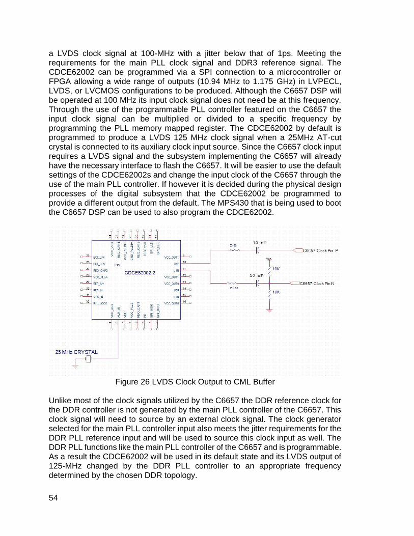
54
a LVDS clock signal at 100-MHz with a jitter below that of 1ps. Meeting the requirements for the main PLL clock signal and DDR3 reference signal. The CDCE62002 can be programmed via a SPI connection to a microcontroller or FPGA allowing a wide range of outputs (10.94 MHz to 1.175 GHz) in LVPECL, LVDS, or LVCMOS configurations to be produced. Although the C6657 DSP will be operated at 100 MHz its input clock signal does not need be at this frequency. Through the use of the programmable PLL controller featured on the C6657 the input clock signal can be multiplied or divided to a specific frequency by programming the PLL memory mapped register. The CDCE62002 by default is programmed to produce a LVDS 125 MHz clock signal when a 25MHz AT-cut crystal is connected to its auxiliary clock input source. Since the C6657 clock input requires a LVDS signal and the subsystem implementing the C6657 will already have the necessary interface to flash the C6657. It will be easier to use the default settings of the CDCE62002s and change the input clock of the C6657 through the use of the main PLL controller. If however it is decided during the physical design processes of the digital subsystem that the CDCE62002 be programmed to provide a different output from the default. The MPS430 that is being used to boot the C6657 DSP can be used to also program the CDCE62002.
Figure 26 LVDS Clock Output to CML Buffer
Unlike most of the clock signals utilized by the C6657 the DDR reference clock for the DDR controller is not generated by the main PLL controller of the C6657. This clock signal will need to source by an external clock signal. The clock generator selected for the main PLL controller input also meets the jitter requirements for the DDR PLL reference input and will be used to source this clock input as well. The DDR PLL functions like the main PLL controller of the C6657 and is programmable. As a result the CDCE62002 will be used in its default state and its LVDS output of 125-MHz changed by the DDR PLL controller to an appropriate frequency determined by the chosen DDR topology.

55
The third input clock for the C6657 required by this design is that of the SRIO / SGMII Reference Clock (SRIOSGMIICLK). At this time the jitter requirements are unknown for this clock source. They are neither listed in the Hardware design guide or the Clocking guide for the C6657. A question regarding this has been posted to the TI E2E forums and as of 4/18/2014 no response has been seen. For now it is assumed that the CDCE62002 will an acceptable solution for this clock input as it is for the other clock inputs of the C6657.
4.3.2. Memory
The C6657 features 2 levels of built in memory at the highest level is the program and data memories. Both of which are built into each of the C6657s 2 cores. These consist of 32KB of memory each per core. Both the program memory and data memory can be set as either cache or SRAM. When used as cache level 1 program memory is direct mapped, while the level 1 data memory is 2 way set associative. Upon reset both of the level one program and data memories are automatically set as caches and will need to be configured if they are desired to be utilized as SRAM. At the second level of the C6657s memory architecture is the 2MB level 2 memory (1 MB per core) and the 1MB Multi Core Shared Memory (MSM). The 2MB of L2 memory can be used as either SRAM, 4 way set associative cache, or as a combination of both. This memory is always set as SRAM upon a reset. The MSM is the most versatile of the memories available on the C6657. It can be configured as a 2nd level memory with the capability to have its contents cached into the L1 program and data memories or as a level 3 memory which can be cached into the L2. The MSM memory can be used a go between for L2 memory and external memory made available to the processor through the use of the External Memory Interface (EMIF). There are 2 EMIFs available on the C6657 a 16 bit EMIF used to provide access to external asynchronous SRAM, and the 32 bit EMIF for interfacing with DDRAM. The 16XEMIF supports both NOR and NAND flash memories in both 16 and 8 bit configurations. Since the device will be capable of simulation different guitar amplifiers and effects there will need to be a place to store the program code. This will be accomplished through the USE of SRAM connected to the C6657 through the 16XEMIF. Currently at this time it is uncertain whether or not the processors combined L1 and L2 memories will be large enough to fully implement the code required by this device. If external RAM is required the C6657 features a built in DDR3 controller among its peripherals. There are several topology’s supported by the DDR3 controller. The smallest of which and what will be implemented if it is determined that RAM is needed is the 8MB X16X 8 banks configuration resulting in 1024 Mb of total memory. To properly set up the DDR3 controller the32 bit DDR_SDRFC register will need to have its lower 7 bits set which correspond to ( In order from Most significant to least significant) IBANK(6:4) EBANK(3:3) PAGESIZE(2:0). Where IBANK corresponds to the number of banks used by the DDRAM. For DDR3 this will always be 8 Banks and correspond to a bit pattern of 100. The page

56
size for 8MBX16X8 1GB configuration results in a page size of 1024 words and will require the PAGSIZE bit pattern to be set to 010. The EBANK portion of the register allows for more than one module of ram to be connected to the DDR3 controller. However in using this configuration this bit will be set to 0. There are 86 pins that must be traced from the processor to the used DDRAM including addresses and data busses, control signals as well as clock signals that will require special attention during the PCB design processes. The number of pins required to support the use of SRAM are however far less resulting in only a total of 51 to accommodate the address and data buses, and control and clock signals. It is highly desirable that the design does not require the use of DDRAM. In not using DDRAM the number of traces can be minimized resulting in the area and or layers needed to implement the processors PCB to be reduced.
4.3.3. Power On and Boot Sequence
When the C6657 is initially turned on it requires that its voltage rails input clock signals be mad availed in a sequential sequence. There are two possible power up sequences one which provides the core logic power before the input and output and another that provides the output before the input. For this design the core before I/O sequence will be used. As described in the power supply design section a MSP430 microcontroller will be used to turn on the voltage rails in the popper order. As each voltage rail become stable clock signals will be allowed to be mad present at different times as well as reset and power on pins of the C6657 asserted. The MSP430 will also be used to set these pins. The time line for the power up sequence is outlined in Table 16 C6657 Power on Sequence.
Sequence Description C6657 PIN
1 Turn on CVDD(Enable the LM10011 and LM21215A-1)
2 Wait 1 second
3 Turn on CVDD1 ( Enable TPS7A8001)
4 Wait 1 second
5 Enable Clock Drivers
6 Turn on DVD1.8 (Enable TPS72515)
7 Wait 1 Second
8 Drive RESESAT Low H5
9 Turn on DVD1.5 (Enable TPS72515) and Drive RESET high
H4
10 Wait 1 second
11 Drive POR High Y18
12 Wait 1 second
13 Drive RESETFULL high J4
Table 16 C6657 Power on Sequence

57
During step 11 outlined in Table 16 C6657 Power on Sequence of the power on sequence the C6657 is configured when the POR (Power-on Reset) pin is asserted. The configuration of the C6657 sets the endian mode, boot mode, and sets up the PCI express peripheral. This is accomplished through the use of 17 input pins. These input pins can have their logic set either by using pull up and pull down resistors, or via an external control source such as an FPG or MCU. Currently in this phase of design and planning it will not be necessary to change the processors configuration. Without the need to have multiple configurations the C6657 can be configured by hardwiring he logic values for the associated configuration pins. This will eliminate the need for an external control device reducing the complexity of the design. The configuration that will be utilized by the C6657 is outlined in Table 17 C6657 Configuration Bits. The C6657 requires that its internal memory be loaded with program and data code. There are several reset conditions which will initiate the boot process. These include the Power-on Reset (POR), Hard Reset, and Soft Reset. The POR will be initiated every time the processor is powered on. During step 11(Seen in Table 16 C6657 Power on Sequence) the processor laches the logic levels seen on the Boot Configuration pins and uses this to determine the selected boot mode. For this design the processor will use the NAND boot mode. In which it will load its boot software from an externally provided NAND flash memory. To lode the boot configuration data on to the processor the C6657 uses a section of code that resides on it ROM known as the ROM Boot Loader. The RBL will look to the external NAND flash memory, transfer the boot code, and automatically configure the processor. According to the data sheet the NAND flash memory used with the C6657 will need to be ONFI compliant and will be the type implemented in this design.
Parameter C6657 PIN Description Value
LENDIAN T25 C6657 endian mode 0 = Bi Endian 1 = Little Endian
1
BOOTMODE[2:0]
U21, T21,
V22
Sets the boot mode for the processor NAND = 011
011
PCIESSMODE[1:0]
W21, V21 PCIE will not be used XX
PCIESSEN AD20 0 = PCIE disabled 1 = PCIE enabled
0
Table 17 C6657 Configuration Bits
4.3.4. Software
All software for the C6657 processor will first be developed on the TMDSEVM6657 development board that uses the TMS320C6657 processor. This will allow for software to be developed while the PCB board design is still being finalized and printed out. The development board allows all the functionality that will be needed

58
to make everything as if it was on its on PCB board. All the code for the C6657 processor will be developed in the C language using Texas Instruments Code Composer v5. The development also allows for debugging with Code Composer to allow for logic tracing and code validation at intermediate steps. In the Figure 27 Amplifier Gain Stages shows the different stages that an analog signal would go through to be amplified. Since there is a natural flow from one end to the other the way to code each amplifier will be to section off this picture for each vacuum tube and create a function that will allow for certain values to be passed through to allow to change that specific values for the vacuum tube. The values that will need to be passed through are the input signal, all resister, capacitor, and power values. This will allow for the function to model to its best ability any vacuum tube. This will also help to cut down code. The vacuum tube function will then be called from the different amplifier functions. This will help model the different vacuum tubes that the signal would travel through to create the proper amplifier effect. The other designs will be for the treble, bass, mid, and volume control stages. These 4 stages will also be functioned out to since the user is able to change these values from the user interface allows for the ability to change the resistor and capacitor levels to best model the amplifier at this stage with the specific user values. The last section in the reference diagram below is the power gain stage which is at the end. This section will also be function out to allow for the need to dynamically change these values when needed for different power gain stages for different amplifier effects. With these different sections for the amplifier modeling there is 6 different functions that will be overall created which will allow for any amplifier to be modeled. Each actual amplifier that will be modeled will have their own function that will run in a loop calling these 6 different functions passing through the proper values to help simulate that specific amplifier. After all the stages for the amplifier the next item is to send it to a model of the speaker cabinet. This is a simple model that will need to send the signal through an RLC circuit which in the software will be its own function.
Figure 27 Amplifier Gain Stages

59
The next is to add effects after the speaker cabinets before it is sent back to an analog signal. For this project the user will be able to model 4 different kinds of effects. The different kinds of effects the user will be able to model is delay, reverb, compression, and chorus. For each of these 4 effects they will have their own functions within the code for easy use to be called from any amplifier to apply the proper effect that the user would.
4.4. User Interface
4.4.1. Hardware Interface
The device will feature an on board user interface mounted to the devices housing. Newhaven displays NHD-2406WG-ATMI-VZ# 240 by 64 pixel graphic display will be used to display an interactive menu to the user. User controls will be mounted next to the graphics display unit which will allow the user to navigate the options that can be implemented by the device. A set of 4 push buttons will be arranged in an evenly spaced cross pattern representing up, right, down, and left. These 4 directional buttons will be used to navigate through the menus options. Next to the 4 directional buttons will be 2 more push buttons representing select and exit. Select will allow the user to select a menu option or enter a sub category of the menu, while exit will allow the user to return to a previous menu category. A micro controller will be used to control the user interface and send data out to the TMS320C6657 DSP chip over a single output pin. To implement the user interface described above a Texas instruments MSP430G2553IPW28 will be used to control the LCD module, generate the menu, receive input from the user controls, and send instructions to the C6657 DSP. The C6657 will receive instructions from the MCU in the form of a unique binary code via its serial port interface peripheral located at pin (SPIDIN) AB14. The SPI peripheral is a synchronous input output port which will be configured in a slave output master input configuration. With the MCU being the slave and the C6657 being the master, this results in 2 of the MCU GPIO pins being used to transfer the instructions code and receive clock input from the C6657.The NHD-2406WG LCD module requires a total of 14 control lines from the MCU. This includes 8 GPIO pins of the MCU to be used for a bi-directional 8 bit data bus, and an additional 6 GPIO pins for various control signals required by the LCD module. The controls for the user interface will implemented via 6 push buttons connected to GPIO pins of the MCU configured in an active low format. The MSP430s input ports cannot tolerate voltage greater than 0.3V above VCC or currents with magnitudes in excess of ±2mA. To prevent damaging the MSP430 all GPIOs used with the active low push buttons will have pull up resistors to VCC. It is recommended by the data sheet the MSP430s power supply voltage VCC be set to a value between 1.8V and 3.6V. With VCC of the MSP430 set to 3V the required pull-up resistor values are calculated in Equation 43 resulting in a resistance of 1500 ohms.

60
𝑅𝑝𝑢𝑙𝑙𝑢𝑝 =3𝑣𝑐𝑐
2𝑚𝐴= 1500Ω
Equation 43 The logic voltage for the MSP430s and LCD modules GPIO pins are given in Equation 44 though Equation 46. If the MSP430s VCC is set to 3V this results in the output pins logic high being 2.7V as given by Equation 44. Using this result with Equation 46 gives a value of VDD equal to 4.9 volts and will be the power supply voltage required by LCD module.
𝑀𝑆𝑃430 𝐿𝑜𝑔𝑖𝑐 𝐻𝑖𝑔ℎ = 𝑉𝐶𝐶 − 0.3
Equation 44
𝑀𝑆𝑃430 𝐿𝑜𝑔𝑖𝑐 𝐿𝑜𝑤 = 𝑉𝑆𝑆 + 0.3
Equation 45
LCD Logic High = VDD – 2.2
Equation 46 Table 18 Pin Assignments of the MSP430G2553IPW28 and Figure 28 User Interface Schematic shows the pin assignments for the MSP430G2553IPW28 and its implementation with the LCD module and C6657 DSP chip.
Figure 28 User Interface Schematic
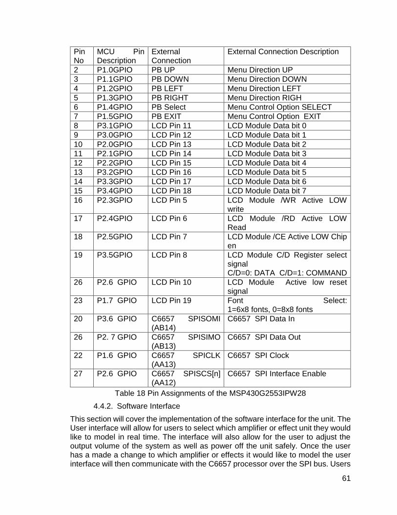
61
Pin No
MCU Pin Description
External Connection
External Connection Description
2 P1.0GPIO PB UP Menu Direction UP
3 P1.1GPIO PB DOWN Menu Direction DOWN
4 P1.2GPIO PB LEFT Menu Direction LEFT
5 P1.3GPIO PB RIGHT Menu Direction RIGH
6 P1.4GPIO PB Select Menu Control Option SELECT
7 P1.5GPIO PB EXIT Menu Control Option EXIT
8 P3.1GPIO LCD Pin 11 LCD Module Data bit 0
9 P3.0GPIO LCD Pin 12 LCD Module Data bit 1
10 P2.0GPIO LCD Pin 13 LCD Module Data bit 2
11 P2.1GPIO LCD Pin 14 LCD Module Data bit 3
12 P2.2GPIO LCD Pin 15 LCD Module Data bit 4
13 P3.2GPIO LCD Pin 16 LCD Module Data bit 5
14 P3.3GPIO LCD Pin 17 LCD Module Data bit 6
15 P3.4GPIO LCD Pin 18 LCD Module Data bit 7
16 P2.3GPIO LCD Pin 5 LCD Module /WR Active LOW write
17 P2.4GPIO LCD Pin 6 LCD Module /RD Active LOW Read
18 P2.5GPIO LCD Pin 7 LCD Module /CE Active LOW Chip en
19 P3.5GPIO LCD Pin 8 LCD Module C/D Register select signal C/D=0: DATA C/D=1: COMMAND
26 P2.6 GPIO LCD Pin 10 LCD Module Active low reset signal
23 P1.7 GPIO LCD Pin 19 Font Select: 1=6x8 fonts, 0=8x8 fonts
20 P3.6 GPIO C6657 SPISOMI (AB14)
C6657 SPI Data In
26 P2. 7 GPIO C6657 SPISIMO (AB13)
C6657 SPI Data Out
22 P1.6 GPIO C6657 SPICLK (AA13)
C6657 SPI Clock
27 P2.6 GPIO C6657 SPISCS[n] (AA12)
C6657 SPI Interface Enable
Table 18 Pin Assignments of the MSP430G2553IPW28
4.4.2. Software Interface
This section will cover the implementation of the software interface for the unit. The User interface will allow for users to select which amplifier or effect unit they would like to model in real time. The interface will also allow for the user to adjust the output volume of the system as well as power off the unit safely. Once the user has a made a change to which amplifier or effects it would like to model the user interface will then communicate with the C6657 processor over the SPI bus. Users
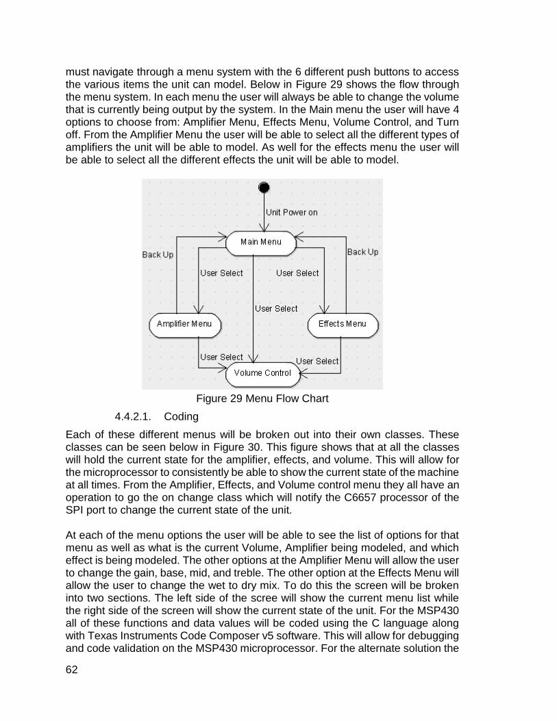
62
must navigate through a menu system with the 6 different push buttons to access the various items the unit can model. Below in Figure 29 shows the flow through the menu system. In each menu the user will always be able to change the volume that is currently being output by the system. In the Main menu the user will have 4 options to choose from: Amplifier Menu, Effects Menu, Volume Control, and Turn off. From the Amplifier Menu the user will be able to select all the different types of amplifiers the unit will be able to model. As well for the effects menu the user will be able to select all the different effects the unit will be able to model.
Figure 29 Menu Flow Chart
4.4.2.1. Coding
Each of these different menus will be broken out into their own classes. These classes can be seen below in Figure 30. This figure shows that at all the classes will hold the current state for the amplifier, effects, and volume. This will allow for the microprocessor to consistently be able to show the current state of the machine at all times. From the Amplifier, Effects, and Volume control menu they all have an operation to go the on change class which will notify the C6657 processor of the SPI port to change the current state of the unit. At each of the menu options the user will be able to see the list of options for that menu as well as what is the current Volume, Amplifier being modeled, and which effect is being modeled. The other options at the Amplifier Menu will allow the user to change the gain, base, mid, and treble. The other option at the Effects Menu will allow the user to change the wet to dry mix. To do this the screen will be broken into two sections. The left side of the scree will show the current menu list while the right side of the screen will show the current state of the unit. For the MSP430 all of these functions and data values will be coded using the C language along with Texas Instruments Code Composer v5 software. This will allow for debugging and code validation on the MSP430 microprocessor. For the alternate solution the

63
AR1000 comes with its own development kit software which will be used to program the user interface which is the AR Configuration Utility (ARCU). This will allow to set up all the different menus and menu options as discussed above.
Figure 30 User Interface Class Diagram
4.4.2.2. Communication
To complete the interface the processor must know which new amplifier or setting that the user has selected. To do this the user interface will communicate to the C6657 processor over the SPI buss. This bus was chosen because its main role is to allow for communication between microprocessors. For this project the SPI buss will be operation in 3-pin option. This is because it is the basic clock for data in and data out SPI interface with a single processor. The 4-pin option allows for multiple SPI slave devices which is not needed since there will only be a single user interface. Below in Figure 31 is the representation of 3-pin SPI option with the master which will be the C6657 main processor and the slave to be the MSP430 microprocessor. This also shows that the C6657 will control the slave clock signal to transmit.
Figure 31 3-Pin SPI

64
For both the master and slave to initiate a data transfer data registers SPIDAT1 which allows for a 16 bit number to be placed in. This then will go over to the master in register SPIBUF to read and decode the number. For this Project there will be a set of numbers that will be defined for the different configurations that could be possible for the user to select. These bit patterns are shown below in Table 19 Bit Patter for SPI Communication.
First 4 Bits Next 8 Bits Control Item
0001 X Amplifier 1
0010 X Amplifier 2
0011 X Effects 1
0100 X Effects 2
0101 X Effects 3
0110 X Effects 4
0111 x Nothing
1000 00000001-1100100 Amplifier Gain Change
1001 00000001-1100100 Amplifier Base Change
1010 00000001-1100100 Amplifier Mid Change
1011 00000001-1100100 Amplifier Treble Change
1100 00000001-1100100 Effects Wet to Dry Change
1101 00000001-1100100 Volume Change
1110 X Nothing
1111 X Nothing
Table 19 Bit Patter for SPI Communication From the Table 19 above you can see how the user will be able to set the different amplifiers or effects. For these selections the last 8 bits will all be set to zero but will not be necessary since the processor will not decode these bits. As well as be able to change the gain, base, mid, treble, and wet to dry values from a range of 1 (bit pattern 00000001) to 100 ( bit pattern 1100100) that will be added to the end of the original 4 bits to tell the difference between which item is being changed. Since the SPI port allows for the 16 bit transmission overall the last 4 bits (since 4 bits are used for the selection and the next 8 for the range from 1 to 100 which gives 12 bits of 16) are also do not care but will be set to zero even though these bits will not be decoded.
4.5. Printed Circuit Board Design
There are several subsystems that make up the entirety of this device, bulk power supply, user interface, analog inputs and outputs, and digital signal processing. To help maintain signal integrity and combat any noise that maybe introduced onto the signal at the various stages of its processing. Each of the sub-systems will be

65
implemented on their own independent printed circuit board. Each board will then be interconnected with each other.
4.5.1. Printed Circuit Board Requirements
As it has been stated many times before one of the primary requirements of this device is to maintain signal integrity at every stage this begins with the power supply and follows through until the final processed audio signal leaves the device. To help maintain signal integrity and prevent noise from being transmitted between each subsystem circuit board counter measures such as electric isolation in the form of optocouplers and filtering may be employed. The device is designed to fit into a 19” Width x 3.5” Height x 17.7”Depth chassis. All 4 sub-system circuit boards will need to fit within these dimensions.
4.5.2. Analog Board
The input output subsystem will be implemented on a single PCB. This board will feature multiple ICs including 1xPCM4222 ADC, 2xPCM1794A DAC, 2xDRV134 line Drivers, and 1xTPA6120A2 headphone amplifier. These device will also require additional external active components such as Opamps to act as input buffers, amplifiers and current to voltage converters. This board will most likely be the second largest implemented by the design second only to digital signal processing subsystem the C6657 DSP chip. Texas Instruments manufactures an Evaluation Module for the PCM4222 ADC. This EVM required the use of a 4 layer 500 x 800 mil (0.5x0.8 inch) board to correctly implement the ADC chip. It is assumed that a board of at least 4 o 5 times that in area as the EVM for the PCM4222 will be required. In addition the EVM is a 4 layer board and will be the assumed number of layers required to implement this designs board.
4.5.3. Digital Board
The digital board is the sub-system which will be used to implement the Keystone TMS320C6657 digital signal processor. The C6657 is a 21-mm by 21-mm plastic BGA package featuring 625 pins. Due the massive amount of pins numerous layers will be required to implement this subsystems PCB. According to the schematic diagrams published by Einfochips the manufactures of the C6657s development board a 12-layer PCB made of FR4_IT168G was required to implement the processor. The development board however is designed to utilize every feature of the C6657 processor for this device not all of the processors capabilities will be utilized. As a result of this it is hopeful that the final PCB design of this sub-system will not require a 12 layer design. Table 20 Peripherals for the C6657 and their uses outlines the 16 available peripherals of the C6657 and their functional use for this devices design.

66
Peripheral Description Function DDR3 Memory Controller (32-bit bus width)
The 32-bit DDR3 Memory Controller bus of the TMS320C6657 is used to interface to JEDEC-standard-compliant DDR3 SDRAM devices
Used to interface with DDR3 SDRAM made availed on the digital sub-system
High-speed 1×/2×/4× Serial RapidIO Port
High Speed Packet Switched Interconnected used for chip to chip and board to board communication
Not used in design
PCIe
The PCI Express (PCIe) module is a multi-lane I/O interconnect providing low pin count, high reliability, and high-speed data transfer.
Not used in design
10/100/1000 Ethernet
Used to transfer data between host and other connected device that are compliant with Ethernet protocol
Not used in design
HyperLink A high speed data communication bus Not used in design
EMIF16X 16 bit External memory interface used to connect to extern flash RAM
Will be used to interface with external NAND flash memory
SPI Serial Port Interface provides high speed synchronous input out
Will be used to communicate with user interface
UART Performs serial to parallel conversion on data received from a connected device
Will not be used in the design
I2C Provides an interface between the processor and other device which support I2C technology
Not used in design
GPIO General-purpose Input Output pins
Table 20 Peripherals for the C6657
4.5.3.1. Hardware configuration of the TMS320C6657
According to the data sheet for the C6657 it is possible to leave pins corresponding to unused peripherals floating without effecting the functionality of the overall device. There will however be a small leakage current of approximately 100-uA at every pin. To prevent these leakage currents pull up or pull down resistors will be implemented at all unused pins. It is also necessary to ensure that any pin routed to a pull up or pull down resistor must never be configured as an output. Some unused peripherals require special care and must have their unused requirements met to ensure proper operation of the processor. The PCIE feature of the C6657 is not needed for the design of this device. Unused pins (W21, V21, and AD20) of the PCIE will be connected to ground via 1-kΩ pull down resistors, and disabled in the memory mapped register. The PCIEs power pin (AA9) will still need to be connected to the VDDR2 power rail. Pins AD14 (PCIECLKP) and AE15 (PCIECLKN) are the power and ground pins for the

67
differential clock inputs corresponding to the PCIE peripheral. Pin AD14 will be need to be connected to the CVDD power rail and pin AE15 will be connected to ground via a 1-kΩ resistor. Ethernet is a feature that will not be utilized by the device. The Serial Gigabit Media Independent Interface and Management Data Input Output is utilized by the Ethernet media Access Controller peripheral of the C6657 and will need to be disabled in the MMR. The SGMII power pin (AA3) will still need to be connected to the peripherals power rail VDDR3. Both the SGMII and Serial Rapid Input Output share the same clock input, because SRIO is utilized by this device its clock configuration will be covered in section 4.3.1 Clocking. The hyperlink feature will not be needed in the implantation of the C6657 on this device. There are 8 pins hyperlink clock and data pins which will be connected to ground via 1-kΩ pull down resistor. The hyperlink peripheral will need to be disables in the MMR and its power pin (M20) will be connected to VDDR1. Pins C25 (MCMCLKP) and B24 (MCMCLKN) are the power and ground pins for the differential clock inputs corresponding to the hyperlink peripheral. Pin C25 will be need to be connected to the CVDD power rail and pin B24 will be connected to ground via a 1-kΩ resistor. The I2C peripheral will not be utilized in the design of this device. Pins AA18 AA17 corresponding to the I2C clock and data respectively will need to be pulled up to the DVDD18 power rail by a 1-kΩ resistor.
4.5.3.2. Filtered Voltage Supplies
There are several voltage regulators that will be used to provide the numerous voltage supplies required by the C6657s core logic and I/O. These regulators will be placed as close to the C6657 as possible and utilizes power planes to router their regulated voltage to each of the necessary power pins. In addition to the 4 core and I/O voltages 3 additional filtered voltages will need to be provided by the CVDD1, DVDD1.5, and DVDD1.8 regulated voltages corresponding to VDDT, AVDDA, and VDDR respectively. An additional 0.75 reference voltage will also need to be made available to the VREFSSL (pin E12) pin of the processor. This voltage can be created through the use of a voltage divider sourced by the DVDD15 voltage rail. According to the hardware design guide for the C56657 it is imperative that resistors with 1% tolerance or better be used to realize the voltage divider. VDDT is a filtered version of the CVDD1 voltage. This voltage will be used to provide termination voltages for the Serial deserializer interface of the C6657. According to the hardware design guide. Each pin group of the SerDes must be connected to the CVDD1 voltage through an individual filter circuit seen in Figure 32 Filter Circuit for Filtered Voltage Connection. The C6657 features two groups of SerDes termination supply pins these are outlined in Table 21 C6657 Pin Connections for Filtered Voltage Supplies.

68
AVDDA is a filter voltage created by the DVD18 regulated voltage used for the core and DDR PLL. For the C6657 this corresponds to only two pins that will need to be connected to this voltage supply. Each pin will need to be connected to AVDDA through an individual filter circuit. The filter circuit used to connect AVDDA to DVDD1.8 is the same as that used for the VDDT voltage and is shown in Figure 32 Filter Circuit for Filtered Voltage Connection VDDR is a filtered voltage created from the DVDD15 voltage and used to provide power to various peripherals supply voltages. Each of the 4 power pins o the C6657 that are connected to this voltage must be connected through an individual filter circuit. This circuit is the same as the other filtered voltage connections and show in Figure 32 Filter Circuit for Filtered Voltage Connection.
Figure 32 Filter Circuit for Filtered Voltage Connection
Core – I/O Filtered Power Supply
C6657 Pin Number
Description
CVDD1 VDDT1 K19, L20, M19, N20
Termination suppl for Hyper Link and SerDes
VDDT2 W8, W10, W12, Y7, Y9, Y11
Terminatin Suply for SGMII , SRIO ,PCIe, and SerDes
DVDD18 AVDDA1,2 Y15 F20 PLL Supply for Core and DDR3
DVDD15 VDDR1 M20 HyperLink SerDes regulator supply
VDDR2 AA9 PCIe SerDes regulator supply
VDDR3 AA3 SGMII SerDes regulator supply
VDDR4 AA5 RIO SerDes regulator supply
VTT E12 VEFSSL
Table 21 C6657 Pin Connections for Filtered Voltage Supplies

69
4.5.3.3. DDR3 Routing
It is uncertain at this time whether or not DDR3 memory will be required by the C6657 to fully realize the design of the device. However if it is special care will need to be taken when routing and laying out the PCB used to implement the C6657 DSP. Due the fact that the DDR3 memory will require a high speed design. There are several aspects of the PCB design process that are outlined by the DDR3 Design requirements for the Key Stone Devices Application report from Texas Instruments that will be followed during the design process. It is suggested that solid power and ground planes be used with DDR3 memory with absolutely no breaks. High speed signal traces will need to be routed between the power planes to reduce electromagnetic interference. In general TI suggest that at least 4 layers be used for routing signals and that the stack up of the PCB layers be symmetric with respect to the top and bottom layers. When routing the address lines form the C6657 DSP to the DRAM module the lines will need to be reference to one of the solid ground planes to provide a low impedance return path. All address lines will also be routed away from the data bus lines. The address traces must not exceed 4.5inches (114.3mm) in length and should be spaced no less than 0.3mm apart. However it is recommended that at least 0.5mm of spacing be provided although this will increase the size of the PCB due to the limited time frame the recommended trace spacing will be used. The control lines for the DDR3 controller like the address control lines will be referenced to a solid ground plane. Unlike the address lines though the control lines will be routed directly from the C6657 DSP to the DRAM module. The best routing method to implement the data lines for the DRAM module is to rout them all on a top layer without the use of any vias. If vias are used there will be added delay in the signal propagation that would need to be considered. The data lines will also be routed adjacent to a solid ground plane.
4.5.4. Bulk Power Supply Board
The bulk power supply will be implemented on a simple two layer printed circuit board. While it would be possible to implement this subsystem on a piece of perf board hand soldering component interconnections would be difficult. It is most certain that any tracks created by hand would be large and require more surface area than those compared to a printed circuit board trace. Since every track acts like a small antenna and has the potential to introduce parasitic, inductance and resistance it is desirable to have as short as tracks as possible. By using a printed circuit board tracks between the component leads can be made much shorter and cleaner than those made by hand. The main power transformer will not be mounted to the printed circuit board implementing the bulk power supply. This decision was made to allow for the printed circuit board to remain as small as possible reducing the overall cost.

70
4.6. Power Supply Design
To properly power the device a bulk power supply will take the 220-V 60Hz mains AC signal from a wall outlet and convert it to a lower voltage DC signal. The overall power system for the device will be designed from back to font meaning the power distribution will be designed for each subsystem before the bulk power supply. First the power consumption and required voltages will be determined for each component used in the design. Next the required supply voltages for each component will be grouped together by magnitude and their required power calculated. Regulators capable of supplying these voltages at the required power will then be chosen. Finally the bulk power supply will be designed to provide a few voltage outputs which in turn will be used to source groups of the different sub-systems voltage regulators. To cut down on possible electromagnetic interference from the bulk power supply regulation of the linear form will be implemented despite its inefficiency and requirement for larger passive components. The bulk power supply will be used to generate several DC voltage rails which will be fed to the various subsystems of the device. These voltage rails will then be used to source other DC to DC LDO step down regulators used to provide the proper supply voltage and power for each component. In designing the bulk power supply for the device the total power consumption requirements for the entire devices hardware design were calculated. While it is straight forward to calculate the power consumption of each individual part used in the design it was slightly more difficult to determine the power consumption of the C6657 DSP chip. The power consumption of the C6657 is not constant and will vary with usage. Obviously the more the processor is working the more power it will require. In addition to this there is also the peripheral usages to consider. The C6657 features a large range of peripherals some of which may or may not be needed, or may be used in varying degrees all of which will effect power consumption. Texas Instrument fortunately provides an excel spreadsheet that allows the user to select what peripherals and the frequencies of their usage to determine the power requirements of the C6657. Currently at the time this document is being written there are some features of the C6657 that are not needed to fully realize the design. However since the final design is not yet completed it was determined that the C6657 should be capable of operating at its full potential with all its features enabled at max usage. In doing this it prevents the power supply design from being a bottle neck in the final design. It would be costly in both time and money to go back and have the power supply PCB redesigned and reprinted. Given the limited time frame to complete this design and the fact that something's will need to be done in parallel such as software development that may or may not require some aspect of the C6657. Over estimating the power requirements was decided to be the best approach when designing the devices power supply. The total power consumption for each component, subsystem and overall design can be seen in Table 22 Device Power Requirements. Once all the required supply voltages and power consumptions for each part used in the design

71
was known the next step was to select DC to DC linear regulators capable of providing the proper voltages and source enough current. The device will feature several printed circuit boards to implement the different subsystems of the design. This includes a board for the analog input output, user interface, and a processor subsystems. In using several printed circuit boards the consumed power for each subsystem or subsystems implement by a single PCB was summed for each individual supply voltage. The results were then divided by the voltages magnitude to determine the required current a regulator will need to be capable of sourcing for each voltage supply. The result of which can be seen in Table 23 Power and Current Requirements for each Supply Voltage. It should be noted that the results in Table 23 do not include the voltage rails needed by C6657, these will be covered in more detail in 4.6.1 Digital Sub System. With the minimum source current and voltage known for each supply voltage regulators could be selected using these two parameters as requirements Table 24 Supply Voltage Regulators outlines the selected regulators and their operating parameters relating to voltage, current, and power.
Sub-System Function Qty PART Supply Volts
quiescent current A
POWER W
INPUT
ADC 1 PCM4222 VCC1 + 4 0.065 0.26
VCC2 + 4 0.065 0.26
VDD + 3.3 0.024 0.0792
Input Buffer 1 OPA827 VSS + 15 0.0052 0.078
VSS - 15 0.0052 0.078
OUTPUT
DAC 2 PCM1794A VCC1 5 0.035 0.35
VCC2R 5 0.035 0.35
VCC2L 5 0.035 0.35
VDD 3.3 0.045 0.297
I/V Converter 2 NE5534 VCC + 15 0.08 2.4
VCC - 15 0.08 2.4
I/V Converter 4 LT1028 VCC + 15 0.0105 0.63
VCC - 15 0.0105 0.63
Stereo Out 2 DRV134 VSS + 15 0.0055 0.165
VSS- 15 0.0055 0.165
Headphone Amp 1 TPA6120A2 VSS + 15 0.015 0.225
VSS - 15 0.015 0.225
UI
UI MCU 1 MSP430G2553 VCC + 3 0.00042 0.00126
Display 1
NHD‐24064WG VSS + 3.5 0.02 0.07
VDD + 5 0.02 0.1
LED + 3.5 0.128 0.448
DSP
Voltage Rail 1 REFLEX CVDD VAR 4.76751
Voltage Rail 1 CVDD1 1 0.78189
Voltage Rail 1 DVDD1.5 1.5 0.32257
Voltage Rail 1 DVD1.8 1.8 0.02343
SR Controller 1 LM10011 VDD + 5 0.00034 0.0017
MCU 1 MSP430G2553 VCC + 3 0.00042 0.00126
Total power consumption of all sub-systems 15.45982
Table 22 Device Power Requirements

72
Board Supply Voltage
Total Power Watts
Total Current Amps
Input Output
3.3 0.3762 0.114
4 0.52 0.13
5 1.05 0.21
15 3.576 0.2384
-15 3.576 0.2384
User Interface
3 0.00126 0.00042
3.5 0.148 0.042286
5 0.02 0.004
Table 23 Power and Current Requirements for each Supply Voltage
Regulator V out
V in min
Vin Max
Vdo+Vout I in I q I out Pin min
Pin max Pout
Volts Amps Watts
TLV70130 3 2.5 24 3.4 0.15003 0.00003 0.15 0.375075 3.60072 0.45
TPS70930 3.3 2.7 30 3.6 0.150001 0.000001 0.15 0.405003 4.50003 0.495
LM1086 3.5 2.6 27 4.8 3.5 2 1.5 9.1 94.5 5.175
LP2985-N 4 2.5 16 4.28 0.150065 0.000065 0.15 0.375163 2.40104 0.6
TPS76850 5 2.7 10 5.23 1.000008 0.000008 1 2.700022 10.00008 5
TL780-15 15 17.5 30 17 1.5055 0.0055 1.5 26.34625 45.165 22.5
LM320-N 15 -18 -25 18 1.504 0.004 1.5 27.072 37.6 22.5
Table 24 Supply Voltage Regulators
4.6.1. Digital Sub System
The Digital sub-system will be used to implement the TMS320C6657 DSP. This processor requires several voltage sources including one AVS (Adaptive Voltage Scaling) source provided by the CVDD voltage rail. This AVS source has its magnitude set based on a 6 bit code sent by the processor to a power supply implementing Texas Instruments SmartReflex Class 0 Technology. The SmartReflex power supply will consist of a LM10011 digitally programmable controller for DC to DC voltage regulators and the LM21215A DC to DC switch mode regulator. The LM10011 will read a 6 bit code sent from the processor over the VCNTL[3:0] bus via the processors tri state pins (from least significant to most significant bit) E22, E23, F23, and G23. The LM10011 digital controller compares the 6 bit code and the output voltage from the LM21215A regulator. A current from the IDAC_OUT pin of the digital controller is then sent to the feedback input pin of the LM21215A regulator causing the voltage regulator to adjust its output based on the magnitude of the current. According to the data sheet for the C6657 CVDD should initialize to a voltage of 1.1V and be capable of supplying voltages in a range from 0.85V to 1.1V (250mV). To obtain this voltage a starting current will need to be set though the use of external hardware for the LM10011 digital controller. This is done with a resistor connected to the set pin of the digital controller. To determine its resistance value the 2 feedback resistors as seen in Figure 33 Texas Instruments SmartReflex Class 0 Power Supply for C6657 will need to first be calculated. To do this
Equation 47 is used to calculate 𝑉𝑜𝑢𝑡_𝐿𝑆𝐵 where resolution is equal to (26) 63 when

73
the LM10011 is operated in the 6 bit mode. Then using the results of Equation 47 𝑅𝐹𝐵_1 can be calculated using Equation 48 where 𝑖𝐿𝑆𝐵 corresponds to 940-nA given
by the data sheet. Initially upon start up the output current of the LM10011 will be
zero (𝐼𝐷𝐴𝐶𝑂𝑈𝑇 = 0) resulting in Equation 49 simplifying and being used to calculate 𝑅𝐹𝐵2. The value for 𝑉𝐹𝐵 is that given by the DC to DC regulator the LM10011 is controlling namely the LM21215A. With required feedback resistor values known
the 𝐼𝐷𝐴𝐶𝑂𝑈𝑇 current can be calculated using Equation 50 and the set pin resistor chosen from table 1 in the LM10011s data sheet.
𝑉𝑜𝑢𝑡_𝐿𝑆𝐵 =𝑉𝑜𝑢𝑡 𝑅𝑎𝑛𝑔𝑒
𝑟𝑒𝑠𝑜𝑙𝑢𝑡𝑖𝑜𝑛=
250𝑚𝑉
63= 0.00396825396 𝑣
Equation 47
𝑅𝐹𝐵1=
𝑉𝑜𝑢𝑡𝐿𝑆𝐵
𝑖𝐿𝑆𝐵=
0.00396825396 𝑣
940 ∗ 10−9 𝑖= 4221.546775Ω
Equation 48
𝑉𝑜𝑢𝑡 = 𝑉𝐹𝐵 ∗ (1 +𝑅𝐹𝐵1
𝑅𝐹𝐵2
) − 𝐼𝐷𝐴𝐶𝑂𝑈𝑇 ∗ 𝑅𝐹𝐵1 ⟹ 𝑅𝐹𝐵2 =𝑅𝐹𝐵1
(𝑉𝑜𝑢𝑡
𝑉𝐹𝐵− 1)
=4221.5Ω
(1.10.6
− 1)= 5065.856 Ω
Equation 49
𝐼𝐷𝐴𝐶𝑂𝑈𝑇 = 1
𝑅𝐹𝐵1
(𝑉𝐹𝐵 ∗ 1 +𝑅𝐹𝐵1
𝑅𝐹𝐵2 − 𝑉𝑜𝑢𝑡) =
1
4222Ω(0.6𝑣 1 +
4222
5066 − 1.1) = 9.35 ∗ 10−9
Equation 50 The calculated IDAC_OUT corresponds to a set Resistor value of 301-ohms.The SmartReflex power supply will be designed using the suggested configuration in Figure 33 Texas Instruments SmartReflex Class 0 Power Supply for C6657 provided by Texas Instruments hardware design manual for the keystone C6657 The C6657 processor in addition to the AVS CVDD voltage requires 3 additional voltages sources, CVDD1, DVDD18, and DVDD15. Each of these voltages will be produced by using DC to DC linear regulation. In choosing regulator models that would be used to provide these voltages several factors were taken into consideration. First of all low noise regulators were desired to prevent as much noise as possible from being introduced to the audio signal. Secondly the TMS320C6657 requires the voltage rails to power up and down in a specific sequence. Resulting in the need for regulators featuring enable pins. Finally to be as efficient as possible and reduce the generation of thermal energy Low Drop Out regulators were chosen. In the end the TPS5725XX and TPS7A8XX family of Texas Instrument linear regulators were selected. These are low noise, LDO, regulators with enable pins. For the DVDD18 and DVDD15 voltages the TPS72518, and TPS72515 fixed voltage regulators respectively were selected. To reduce the complexity of the design and keep things as simple as possible

74
solutions to provide power to the C6657 implementing fixed linear regulators were initially sought after. Unfortunately no fixed regulator could be found that would provide both the regulated 1-V output and required 0.78189 watts or power for the CVDD1 voltage rail. To meet the demands of the CVDD1 voltage the TPS7A8001 variable linear regulator was selected. Like the other regulators used in this sub-system it too has LOD and low noise characteristics. Table 25 Power Characteristics of Regulators Utilized by C6657 outlines the selected regulators used to power the C6657 and their characteristics relating to power consumption and source capabilities. In comparing the Pout column of Table 25 with that of the power column of Table 22 it is clear that this is an acceptable solution to the C6657s power requirements.
Figure 33 Texas Instruments SmartReflex Class 0 Power Supply for C6657
Regulator V out
V in min
Vin Max I in
quiescent current
I out Pin min Pin max
Pout max
Volts Amps Watts
TPS7A8001 1 2.2 6.5 1.00006 0.00006 1 2.200132 6.50039 1
TPS72515 1.5 1.8 6 1.00007 0.00007 1 1.800126 6.00042 1.5
TPS72518 1 1.8 6 1.00007 0.00007 1 1.800126 6.00042 1
LM21215 5.5 2.95 5.5 0.003 4.76751
Total Consumption By Regulators and Total Possible Sourced Power 5.800384 18.50123 8.26751
Table 25 Power Characteristics of Regulators Utilized by C6657 Being that the TPS7A8001 regulator is variable it will need to be configured for the desired output of 1-V using external resistors connected to the feedback pin. The output voltage is calculated using Equation 51. It is suggested by the data sheet of this regulator that smaller values with 1% tolerance be used to reduce the

75
amount of noise injected into the feedback pin. From table 2 of the data sheet the suggested resistor values of 2.94KΩ and 10KΩ were selected.
𝑉𝑜𝑢𝑡 =(𝑅𝐹1 + 𝑅𝐹2)
𝑅𝐹2∗ 0.8 => (
2.94𝐾 + 10𝐾
10𝐾) ∗ 0.8 = 1.0352𝑉
Equation 51
4.6.1.1. Power On and Off Sequencing
To properly power on the keystone TMS320C6657processor the core logic will be provided before the input output voltages. This power on sequence requires that CVDD is first enabled followed by CVDD1 then DVDD18 and finally DVDD15.When the processor is powered off the same sequence is used except in the reverse. To implement the power on and off sequences a MSP430G2553 microcontroller will be included on the digital subsystem. When the user turns on the device via a master switch on the power supply. The microcontroller will then turn on CVDD by sending a high signal to the LM1011 digital controller and LM21215Aswitch mode regulator enable pins. The microcontroller will then sequentially enable each of the reaming linear regulators. When the user wishes to power down the device the microcontroller will simply remove the enable signal from the voltage regulators but in the reverse order. While the device will initially be powered on by toggling the master switch on the main power supply. To properly shut down an option to power off the device will be implemented in the user interface. In doing this the C6657 can properly power down before power is removed from the entire device. A 28 pin DIP package MSP430G2553 microcontroller will be programed using the Texas Instruments MSP430 launch pad. The microcontroller will then be removed from the launch pad and placed onto the digital sub-system via a 28 pin socket mounted on the printed circuit board.
4.6.2. User Interface Sub System
The user interface will consist of a LCD module, a MSP430G3553 microcontroller and a set of controls. This sub-system will be implemented on its own printed circuit board and will require 169.26-mW of power. The New Haven DisplaysNHD-24064WG 264X 64 Parallel pixel graphic LCD module was selected for the device’s user interface. This LCD requires a 5-V 0.1-W power supply, and a 3.5-V 035-W source for its backlight. In addition to the two voltage sources used by the LCD the MSP430 will require a 3-V 1.26-mW source. The user interface sub-systems3, 3.5, and 5 voltages will be supplied by the TLV70130, TLV70235, and TPS76850 linear regulators respectively. The parameters of these regulators are outlined in Table 24 Supply Voltage Regulators.
4.6.3. Input Output Sub System
This sub-system will be built onto a signal PCB and feature both analog to digital and digital to analog converters. These are complicated devices that require

76
multiple supply voltages and the use of external active components such as operational amplifiers. The input portion of sub-system will feature the PCM4222 duel channel 24-bit analog to digital converter. This particular ADC requires 2, 4-V 65-mW and 1, 3.3-V 24-mW power supplies. These three voltages will be supplied by the LP2985-N and TPS70930 linear regulators respectively. The PCM222 ADC requires the use of an input buffer capable of supply a differential input audio signal as discussed in section 4.1 Audio Inputs and Outputs 2 OPA827s Opamp connected in an inverting series configuration will be used to accomplish this. To allow for these Opamps to have both positive and negative voltage outputs both a positive and negative voltage rail of 15-V capable of sourcing 156-mW will be required. The Opamps used as an input buffer to the ADC are not the only components on this sub-system requiring the use of ±15-V supplies. The 2 PCM1794A DACs used at the output will require multiple Opamps to convert their output currents to voltages. This will include 4 LT028 Opamps requiring ±15-V at 157.5-mW per voltage supply and 2 NE5534 Opamps requiring ±15-V at 1.2-W per voltage supply. In addition to these Opamps. The TPA6120A2 headphone amplifier and DRV134 line driver also require ±15-V voltage supplies. In total the voltage regulators used to provide both the positive and negative regulated 15-V will need to be capable of sourcing 3.576-W each. To accomplish this theTL780-15 will be used for the positive rails while the LM320-N will regulate the negative rail. The voltage regulators and their characteristics implemented in this sub-system are outlined in Table 24 Supply Voltage Regulators.
4.6.4. Bulk Power Supply
With the Input Output board being the only sub-system requiring ±15-V this voltage will be provided by 2 regulated voltages from the bulk power supply. Rather than on board DC to DC regulators which would also in tern need to be sourced by the bulk power supply. These two voltages will be supplied by the TL780-15, and LM320-N. The three regulators (TPS70930, LP2985-N and TPS76850) implemented on the input and output board are outlined in Table 24 Supply Voltage Regulators. The input voltages for these three regulators will be sourced by a single regulated output of the bulk power supply. The regulated output will need to in magnitude of at least 5.23-V and less than 10-V so as to exceed the highest dropout plus output voltage ratting of the three sourced regulators, and not exceed the lowest input voltage of the three sourced regulators. In addition the sourcing regulator will need to be capable of providing enough power at the given voltage. To accomplish this theUA7808 by Texas Instruments was selected. This regulator provides 7.7-V at a maximum of 11.55-W exceeding the required 3.5-W and 5.23-V input. The user interface subsystem utilizes regulators that have very similar operating parameters as those used in the input output sub-system. The highest Vdo+Vout is identical to that of the one seen on the input output board. As a result of this the

77
same UA7808 regulator sourcing the input output board will also be used to provide regulated 7.7-V dc signal at 1.18-W. By far the most power consumption will be from the DSP subsystem totaling 5.8954-W. Due to the need to impairment the SmartReflex power supply for the C6657 the LM21215 switch mode power supply will be required. At its maximum out the LM21215 will need to source 4.76751 watts of power. With an input voltage of 5 volts, and input current of 4.5637 amps the total input power to the LM21215 will require 22.81855263 watts of power. This will be sourced from the bulk power supply using a LM1084 linear regulator. In addition to the SmartReflex Supply several other voltage rails will need to be powered by the bulk power supply. This will be accomplished through the use the TPS7A4525 2.5-V which will provide an input voltage for the regulators creating the 1, 1.5 and 1.8 voltage rails. Table 26 Power Requirement for Source Regulators of the Bulk Power Supply.
Sourcing Regulator
Max Ratings Sourcing Regulator
Sourced Regulator
Sub-System
Vin min Volts
Reg P in Wats
UA7808
7.7 Vout TPS70930 I/O 3.6 0.8778077
25 Vin LP2985-N I/O 5.3 1.0015005
9.7 Vdo+Vout TPS76850 I/O 5.23 1.6170616
1.5 A I out TLV70130 UI 3.4 0.003465
0.0043 mA Iq LM1086 UI 4.8 1.139831
TPS76850 UI 5.23 0.0308616
Required Pout Watts
2.48546
TPS7A4525
2.5 Vout TPS7A8001 C6657 1.25 1.954875
30 Vin TPS72515 C6657 1.67 0.537791667
17 Vdo+Vout TPS72518 C6657 2.01 0.032716667
1.5 A Iout TLV70130 C6657 3.4 0.001125
0.0055 mA Iq
Required Pout Watts
2.526508
LM1084
5 Vout LM21215 C6657 22.81855263 22.81855263
27 Vin
6.5 Vdo+Vout
5 A I out
0.005 mA Iq
Required Pout Watts
22.8185526
TL780-15
15 Vout
+15 Volts I/O 4.203 4.203 30 Vin
17 Vdo+Vout
1.5 A Iout
0.0055 mA iq
LM320-N
-15 Vout
-15 Volts I/O 4.176 4.176 -30 Vin
-12 Vdo+Vout
1.5 A Iout
0.0055 mA Iq
Table 26 Power Requirement for Source Regulators of the Bulk Power Supply With linear regulators used to provide outputs of the bulk power supply selected. A transformer capable of sourcing an input voltage that does not exceed the smallest maximum input voltage, but exceeds the largest Vdrop_out+Vout can be

78
selected. Looking at the 5 regulators and their voltage input ratings an input voltage of 18-V was selected. With the input voltage known selected their required input power can be calculated and the necessary transformer specifications determined. Table 27 Regulators Implemented on Bulk Power Supply outlines the power supplies regulators and their characteristics. The total input power for the 5 regulators using an 18-V input that will be directly sourced by the transformer was calculated to be 115.087-W. Finally using this voltage and power ratting a transformer can be selected that is capable of sourcing enough current and providing ±18-V.
Regulator V in
V out Vdo
Vdo+Vout I in I q I out Pout P in
UA7808 18 7.7 2 9.7 0.610862 0.0043 0.606562 4.670527 10.995516
LM1084 18 5 1.3 6.3 4.568710526 0.005 4.563711 22.81855 82.23678947
TPS7A4525 18 2.5 0.3 2.8 1.011603333 0.001 1.010603 2.526508 18.20886
TL780-15 18 15 2 17 0.2335 0.0055 0.228 3.576 4.203
LM320-N -18 15 3 -12 0.232 0.004 0.228 3.576 4.176
Total Input Power 114.72
Table 27 Regulators Implemented on Bulk Power Supply When considering what type of transformer to use in the bulk power supply two options were considered toroidal and laminated steel core. A toroidal transformer when compared to the laminated steel core variant produces less noise, is about half the size, and weighs about half as much. With the reduction of noise being a constant consideration in every aspect of the design the toroidal transformer variant was determined to be the best option despite of its slightly higher cost. A 115 to 230 V AC primary winding with 18 to 36 V AV secondary winding parallel toroidal transformer from Triad Magnetics rated at 160 VA was chosen. This 160-Watts of power is 39% in excess of what is required by the overall design, and will be more than sufficient for the current design plans. Having the 39% extra available power will also allow for changes in the devices design that may have required a redesign of the power supply if this headroom had not been made available. It should be noted that this particular transformer has a secondary parallel winding configuration and is either capable of outputting 18-V AC in a parallel connection, or 36-V AC in series confection. By using the 36-V AC series connection the transformer will be able to provide an output of ±18-V peak AC. The output of this transformer will be rectified by a full bridge rectifier and filtered by electrolytic capacitors to produce an unregulated DC signal. This unregulated DC signal will not be a continuous signal and will have some ripple voltage that is determined by the size of the filtering capacitors. By limiting the ripple voltage to 1-V the input voltage to the regulators will not drop below the lowest actable level of input of 17-V determined by the TL780-15 used to source the positive 15-V output. Through the use of Equation 52 the size of the filtering capacitors were determined to be 37000uF.

79
𝐶 = 𝐼 ∗ Δ𝑡
Δ𝑉= >
4.44𝐴 ∗1
120 𝐻𝑧1𝑉
= 0.037𝐹 = 37000𝑢𝐹
Equation 52 This value of capacitance is an extremely large one and would require physically large and economically expensive capacitors. Rather than use a single 37000uF filtering capacitor several smaller and much cheaper 18000uF capacitors will be placed in parallel to provide the overall necessary capacitance. To protect the device from excessive currents that may result from an accidental short a fuse will be placed on the transformers primary side in line with. In addition to short circuit current protection varistor will be implemented to protect the device from transient pulses that may appear on the main line current coming from the wall outlet. As it is the function of this device to process audio signal integrity and the rejection of noise is a major concern in every design aspect of this device. The power supply is no exception to this. By using a common mode chock on the transformers secondary noise produced by the main line from the wall outlet can be reduced. The design of the bulk power supply can be seen in Figure 34 Bulk Power Supply Schematic.
Figure 34 Bulk Power Supply Schematic
5. Design Summary
5.1. Hardware
The entire system will consist of the 2U chassis that will store the PCBs that contain the DSP, power supply, and analog input and output boards as well as mount user interface. There will be three PCB boards in the unit. One will be at least a six layer board that will make all the connections for the DSP to other peripherals and the power supply. There will need to be a connection made from this board to the
80
analog board to receive and transmit digital data from the data converters. The board then needs to connect to the user interface so as to be able to communicate with the user interface module. Then this board needs to be connected to the power supply in order to receive the power for the device to run. The next board will contain the analog components responsible for receiving and sending the analog signals as well as sending and receiving digital data to and from the DSP. The analog board will need to receive power from the power supply board. The user interface board will connect to the DSP and receive and send signals to the MSP430 that is populated on the user interface board. The MSP430 will be responsible for controlling the LCD screen and push button interface. All boards will need to accept power from the power supply board. The TMS320C6657 has multiple ports available on the processor in order to interface with memory, data converters, LCD screens, etc. For this design the processor needed to use the McBSP, SPI bus, EMIF16 bus, and the EMIF 32 bus DDR3 interface. The McBSP is a bus that was designed with audio data converters in mind. The port will allow the design to seamlessly interface the data converters to the TMS320C6657. The data converters will be connected via three lines in order to receive and send data to the McBSP. The SPI bus will be utilized to interface with the MSP430. The EMIF16 will be used to interface with the flash memory that is needed to store program data. The DDR3 controller and EMIF 32 interface is needed due to the fact that the DSP does not have enough on board memory to operate the algorithms being used in the DSP. The only input needed for the device is for the input of an electric guitar into the device. From there the signal will be first transformed from an unbalanced signal to a balanced signal via two OPA827 operational amplifiers. The PCM4222 has the ability to receive a differential input signal which will help the overall noise performance of the system. After the signal has been processed by the DSP the digital signal will be sent to two PCM1794A D/A converters. One converter will send a signal to a stereo line driver for output to a PA system. The other D/A converter will send its signal to a headphone amplifier where the user will have the option to connect a pair of headphones for personal reference. The user will also have the option of being able to control the overall volume output of the amplifier. The line driver will not need to be volume controlled so nothing further will need to be done to the circuit. The chassis that will hold all of the PCBs will be a 2U rack mountable housing. This will give the user the ability to mount the housing in a rack module in order to keep the device secure and allow the device to be safe from an accidental drop while being transported. The TMS320C6657 will also require a fan and a heat sink in order to keep the device at a safe operating temperature.

81
5.2. Software
5.2.1. DSP
The C6657 processor will be able to apply a range of various different effect filters as well as model different amplifiers. These operations will be optimized for efficiency and run time using appropriate data structures. The C6657 processor will use the Sys/bios real time operating system provided by Texas Instruments. The C programming language will be used to develop the various algorithms to be used on the C6657 processor. This language was chosen because not only is it supported by the Sys/bios real time operating system but it also designed to optimize the running of the C applications. For each amplifier there are various parameters that need to be calculated in order to define what type of amplifier that needs to be applied to the input signal. These mathematical operations along with defining parameters must meet a time requirement to make sure that the user will not notice a lag from the time they play to the time they hear the sound. To receive the signals an interface with the analog to digital converters and the digital to analog converts will need to be developed. This communication with the ADC and the DAC will happen over the McBSP port
5.2.2. User Interface
The user interface will be programmed on an MSP430 that will control the user interface. The MSP430 will control the 264 x 64 pixel graphic LCD as well as several push buttons. The MSP430 will be programmed in the C language. This language was chosen because it is not only supported but will be optimized to run the code to control the user interface. This will allow the MSP430 to show all the various characters to the LCD screen as well as control the push buttons to change the menu options depending on the button. After the user interface is created the next step is to make the communication from the user interface to the C6657 processor. To do this the SPI port will be used. This port will use 4 pins on the MSP430. The MSP430 will be the slave with the master being the C6657 processor. The alternate solution for the user interface is to use the AR1000 touch screen development kit as on overlay for the LCD screen to get rid of the push buttons. This will allow for touch screen capabilities for the user. To code for this interface the AR1000 comes with its own ARCU software kit that allows to program the user interface.
6. Prototyping
6.1. Software Algorithms Optimization
To help make sure that this project will perform at its specific requirements stated above there will need to be significant optimization to the algorithms. Since the unit must be able to model the specific amplifier and effects under 3 ms we must make sure that all the algorithms are at their most efficient and optimized state. Since this project is to be completed in a small time crunch which is the summer of 2014 a development board will be used. This will allow for the testing of the code on the C6657 processor while the PCB board design is being finalized and put together. The development board that will be used for this project is the TMDSEVM6657LS
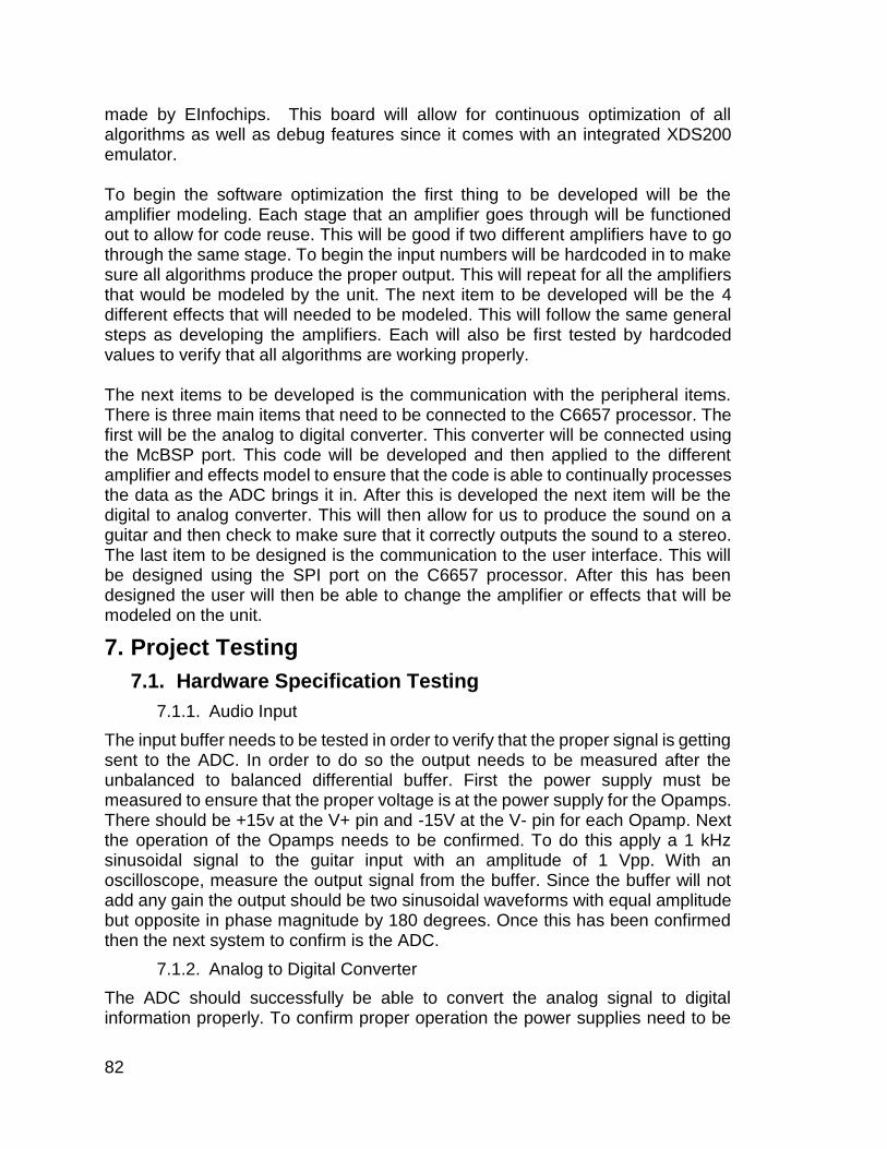
82
made by EInfochips. This board will allow for continuous optimization of all algorithms as well as debug features since it comes with an integrated XDS200 emulator. To begin the software optimization the first thing to be developed will be the amplifier modeling. Each stage that an amplifier goes through will be functioned out to allow for code reuse. This will be good if two different amplifiers have to go through the same stage. To begin the input numbers will be hardcoded in to make sure all algorithms produce the proper output. This will repeat for all the amplifiers that would be modeled by the unit. The next item to be developed will be the 4 different effects that will needed to be modeled. This will follow the same general steps as developing the amplifiers. Each will also be first tested by hardcoded values to verify that all algorithms are working properly. The next items to be developed is the communication with the peripheral items. There is three main items that need to be connected to the C6657 processor. The first will be the analog to digital converter. This converter will be connected using the McBSP port. This code will be developed and then applied to the different amplifier and effects model to ensure that the code is able to continually processes the data as the ADC brings it in. After this is developed the next item will be the digital to analog converter. This will then allow for us to produce the sound on a guitar and then check to make sure that it correctly outputs the sound to a stereo. The last item to be designed is the communication to the user interface. This will be designed using the SPI port on the C6657 processor. After this has been designed the user will then be able to change the amplifier or effects that will be modeled on the unit.
7. Project Testing
7.1. Hardware Specification Testing
7.1.1. Audio Input
The input buffer needs to be tested in order to verify that the proper signal is getting sent to the ADC. In order to do so the output needs to be measured after the unbalanced to balanced differential buffer. First the power supply must be measured to ensure that the proper voltage is at the power supply for the Opamps. There should be +15v at the V+ pin and -15V at the V- pin for each Opamp. Next the operation of the Opamps needs to be confirmed. To do this apply a 1 kHz sinusoidal signal to the guitar input with an amplitude of 1 Vpp. With an oscilloscope, measure the output signal from the buffer. Since the buffer will not add any gain the output should be two sinusoidal waveforms with equal amplitude but opposite in phase magnitude by 180 degrees. Once this has been confirmed then the next system to confirm is the ADC.
7.1.2. Analog to Digital Converter
The ADC should successfully be able to convert the analog signal to digital information properly. To confirm proper operation the power supplies need to be

83
checked. Measure the analog pin and confirm that 5V is applied to this pin. Next check to make sure that the digital pin has 3.3V. Once the power supplies have the proper voltage the next thing to check is the system clock. Measure the system clock pin with an oscilloscope to verify if there is a clock signal present. A periodic square wave should be present at this pin. Once the system clock is confirmed to be present then check to ensure that data is being sent. The left/right clock, bit clock, and data should all be checked. The bit clock and left/right clock should be 128 multiples of one another. To test the data line the same input used for testing the audio inputs should be used. Using an oscilloscope it should be apparent that data is being sent. If data is being sent to and from the DSP than there exists a good connection.
7.1.3. Digital to Analog Converter
The power supplies need to be verified before testing if the DACs are receiving any data. The analog pin should receive 5V from the power supply. Once measured and confirmed using a digital multi-meter test the digital pin. If 3.3V are present then the DACs are receiving the proper voltage. The system clock will need to be measured in the same manner as the ADC clock. Once the clock is confirmed, then the data being sent to the DACs needs to be confirmed. Apply the same 1 kHz sinusoidal signal with an amplitude of 1 Vpp to the input of the audio buffer. Once the processor has finished processing the incoming signal than the procedure for testing the data being received will be the same as the ADC. Once the left/right clock, the bit clock and the data lines have been confirmed using an oscilloscope, then the output buffers need to be tested.
7.1.4. Audio Output
There are two stages to the output for both the headphone amplifier and line driver circuit. The first stage is the current to voltage converters. The output of these converters should be confirmed using an oscilloscope. The next stage is either going to be the headphone amplifier or the line driver. Test each output as there should be the same 1 kHz signal that was sent into the device being sent out of the device. The maximum output for the line driver should be 1.228Vrms. The headphone amplifier will need to be tested by turning the potentiometer use to set the gain and testing if the amplitude modulates. If the signal output is a 1 kHz signal with a 1Vpp magnitude than the device is working as it should.
7.1.5. Power Supply
Due to the fact that the board used to implement the C6657 DSP chip will undoubtedly carry a heavy price tag precautions will be taken to ensure that the subsystem is not damaged by the improper operation of the power supply. Prior to the power supplies implementation with the rest of the design it will be tested to ensure it is operating properly. If garbage is put into the device garbage will be seen at the output of the device. There are 4 regulated voltages produced by the bulk power supply. Each of these will be tested to determine its percent regulation. To do this the load voltages will be measured via a multi meter at no load full load and half load impedances. The

84
half load and full load impedances will be calculated based on the theoretical regulated output voltage along with the maximum and half maximum required currents using Equation 53. These impedances are outlined in Table 28 Power Supply Test Loads. Once each regulator has had its various load voltages measured Equation 54 will be used to determine the respective percent regulations of each regulator both at half load and full load.
𝑅𝑙𝑜𝑎𝑑 = 𝑉𝑟𝑒𝑔𝑢𝑙𝑎𝑡𝑒𝑑
𝑖max/
12
𝑚𝑎𝑥
Equation 53
𝑃𝑒𝑟𝑐𝑒𝑛𝑡 𝑅𝑒𝑔𝑢𝑙𝑎𝑡𝑖𝑜𝑛 = 𝑁𝑜 𝐿𝑜𝑎𝑑 − 𝐿𝑜𝑎𝑑
𝐿𝑜𝑎𝑑∗ 100
Equation 54
Regulator Output Voltage
Half Max Current Amps
Half Load Impedance Ohms
Max Current Amps
Full Load Impedance Ohms
UA7808 7.7 0.1613935 47.70948 0.322787 23.85474
TPS7A4525 2.5 0.5053016 4.94754 1.0106032 2.47377
LM1084 5 2.28185526 2.191199 4.56371052 1.0956
TL780-15 15 0.1192 125.8389 0.2384 62.91946
LM320-N -15 0.1192 125.839 0.2384 62.9195
Table 28 Power Supply Test Loads To facilitate the testing of the power supply at the load impedances calculated in Table 28 Power Supply Test Loads. Two small test boards will be built one for the maximum load ratings and the other for the minimum load ratings. Each test board will featuring a single resistor corresponding to the calculated value for each of the 4 regulators. A connector will be used to connect the board to the output of the power supplies regulators. Then by using a multi meter the load voltage will be measured for each regulator at the corresponding load resistance. Most of the regulators that have their input voltage source by the regulators of the bulk power supply feature max input voltages that are substantially higher than the output voltages of their sourcing regulators. The TPSXX family of regulators used on the DSP subsystem however do not have very high maximum input voltage ratings. The highest being that of the TPS7A8001 with a max of 6.5V. These TPSXX regulators will be sourced by the LM1084 with a fixed output voltage of 5 volts. If this regulator were to have a spike in output voltage of at least 1.5v the regulators used on the DSP board could be damaged and in turn damage the components mounted on the board namely the C6657. The maximum and minimum voltage ratings for each of the subsystems regulators are listen in Table 29 Subsystems Voltage Regulators Max Voltage Ratings.

85
To test the ripple at the output of the sourcing regulators the power supply will be connected to the test boards designed for testing the percent regulation at both half load and full load. The ripple voltage if any seen at the output of each regulator will be measured using an oscilloscope. These varying output voltages will be compared with the maximum and minimum input voltages for each regulator to endure proper operating conditions.
Bulk Power Supply Regulator Sourced Regulator V in min V Vin Max V
UA7808 TLV70130 2.5 24
TPS70930 2.7 30
LM1086 2 2.7
LP2985-N 2.5 16
TPS76850 2.7 10
LM1084 LM21215 2.95 5.5
TPS7A4525 TPS7A8001 2.2 6.5
TPS72515 1.8 6
TPS72518 1.8 6
TLV70130 2.5 24
Table 29 Subsystems Voltage Regulators Max Voltage Ratings
7.1.6. User Interface Hardware Testing
To control the onboard user interface the MSP430G3553 28 pin TSSOP package will be used. Through the use of the MSP-TS430PW28 development board the software required to generate the graphical user interface and communicate to the processor can be developed and tested. This dev board features break out pins which can be used to interface the MSP430s dev board to the LCD display and 6 push buttons needed to implement the devices onboard UI. Once the code has been properly developed to display the menus on the user interface and allow for a user to navigate through them with the use of the push buttons. The portion of code to communicate with the C6657 processor will be developed. It is planned to communicate to the C6657 DSP with the MSP430 through the use of the synchronous SPI interface available on both the MSP430 and C6657. To test the communications software a second MSP430 can be used to simulate the C6657 in a master to slave SPI configuration. This second MSP430 will not need to be the MSP430G3553 28 pin TSSOP package but instead can be the MSP430G3553 20 pin DIP package. In doing this the cheaper launch pad development board can be used to implement the MSP430 simulating the C6657 rather than the more expensive dev board needed for the 28 TSSOP pin variant. To test the communication code signals will be sent from the 28 pin to the 18 pin MSP430 just as they would between the C6657 and the UI. Once the message is received and decoded multiple LEDs will be used to display an encoded message determined during the software development phase. For instance if the user increases the volume via the user interface. The MSP430 simulating the C6657 will illuminate a predetermined pattern of LEDs to show that the volume is being increased. When

86
it is confirmed that the software is properly working the MSP430 28 pin dev board will be interfaced with the C6657 Dev boards SPI to ensure it is possible to control the DSP in this manner. Once the software deployment phase for the user interface is completed a mockup of the user interface will be constructed using perf board with the exact parts intended to be used in the final design. The prototyped UI will then be tested with the C6657 development board to ensure the design works properly. The maximum and minimum logic voltages are outlined in Table 30 C6657 SPI Logic Voltages are those required by the C6657 for proper operation of the SPI peripherals input pins. In the design of the User interface the MSP430 was decided to be powered by Vcc set at 3V and Vss set to 0V. In doing this its logic output voltage levels for each of its pins can be calculated from Equation 55 and Equation 56
𝑉𝑂𝑢𝑡 𝐻 = 𝑉𝑐𝑐 − 0.3𝑉 = 2.7𝑉
Equation 55
𝑉𝑂𝑢𝑡 𝐿 = 𝑉𝑠𝑠 + 0.3𝑉 = 0.3𝑉
Equation 56 While the expected voltage levels for the output logic of the MSP430 exceed the required minimal level for a high signal and do not exceed the maximum level for a low signal. To ensure that proper communication takes place between the UI prototype boards and to prevent damaging the C6657. The UI prototype will be tested to make sure these minimum and maximum ratings are not exceeded before it is interfaced with the DSPs development board.
Parameter Min Max Units
Logic Voltage High 1.17 Volts
Logic Voltage Low 0.63 Volts
Input Current -5 5 uA
Table 30 C6657 SPI Logic Voltages
7.2. Software Algorithm Testing
This section will cover the various test that will be needed to make sure that the digital guitar amplifier and effects unit is working properly. There are two main parts to test for this which are the C6657 DSP by itself as well as the user interface. The man part we are testing for is efficiency to make sure that everything can be ran under 3 ms as well as performance.
7.2.1. DSP
For the C6657 processor we will be testing three major components to make sure that they all work. The different components are amplifier modeling, effects modeling, and proper communication with the various devices hooked up over ports. For each of these components we will first test for accuracy to make sure that all components are working properly and that they are functionally properly

87
and that they are giving the expected results. Then they will be tested for their efficiency in being able to run that model to make sure that every model is meeting our time requirement and that there is no lag in the system. The first component that we will be tested is the amplifying model. For each of the amplifying models we will first test them as their individual model under standard conditions to make sure it produces the right sound as well as to make sure it is under our time requirement of 3 milliseconds. This will be validated in two ways by first making sure that the algorithms in the digital processor are outputting the correct signal number. This will check to make sure that the algorithms are providing answers that are to be expected. The next test will be to play both the digital guitar amplifier next to the actual amplifier unit with vacuum tubes to validate that the sound being produced is the actual sound that should be produced. This test will then be repeated again while having the user adjust one of the five different components of an amplifiers conditions. The five different components that will be individually tested are gain, base, mid, treble, and volume controls. All of these components must pass the two step validation as stated above. Once that all of these components are tested the last test is to test the robustness of the amplifying model by changing each of the five components of each amplifier model to extreme ends to make sure that they also pass the two step validation. If all these components give us their expected number value as well as sound then we will have meet our requirements for this project. The next component that will be tested is the effect modeling. For each of the effects models the first test will be to individual model under standard conditions to make sure it produces the right sound as well as to make sure it is under our time requirement of 3 milliseconds. The validation of the effects model will be done in a two-step process. The first step is to make sure that at the end of the algorithm the proper number in the digital processor are being outputting. The second step is to then make sure that the proper sound is being outputted by playing the digital effects unit next to the actual effects unit we are modeling to hear if the sounds are the same. After the individual testing of the components the next testing will be to change the conditions of the effects unit. There are two components that will be able to change on the effects unit the wet to dry mix and the volume. For each of these components we will take the two step validation stated above to make sure that everything is working properly. After this the next testing will be to make sure that the effects model is robust. To test for this both of the components will have their numbers changed at the same time to their extremes to validate that the system is still producing the proper numbers and the proper sound. The last component for the DSP is to validate the communications. There are four components that are interfaced with the DSP which are user interface, analog-to-digital converter, digital-to-analog converter, and external memory. Each of these components need to be validated to make sure that the right digital signal is being passed on and processed. To test each of these components they will be hooked up to the device individually and then send signals over their various peripheral

88
ports that have been selected. To validate all components excluding the digital-to-analog converter from this test is to send a signal to the processor and then we will check this signal at the processor to make sure that the expect value arrives. The digital-to-analog converter will have to be validated by sending a continuous signals from the processor to the converter and then on an oscilloscope check the output signal to validate the right signal is being produced.
7.2.2. User Interface
For the user interface there are two major components that need to best tested. The first component that is test is the responses from the user. This makes sure that the MSP430 and the LCD screen are displaying the proper items on the screen at all times. To test for this condition the unit will be set up without the connection to the C6657 main processor. We will then begin to press the various buttons and validate that the navigation through the various menu items follows the flow chart in Figure 29. The next item that will be tested is that the proper data is being displayed of the current state of the machine. Since the user can consistently change the amplifier, effects, and volume. To test this the state of the unit will continually be changed to make sure that the screen will always show the proper state after each change. The last component to test is the communication from the user interface with the C6657 processor. This communication will be done over the SPI peripheral port. For this communication there will be predetermine bit patterns that the C6657 will be able to process. Table 19 Bit Patter for SPI Communication shows the patterns that the C6657 processor to decode which will corresponds with the various items that the user interface can change. The ‘X’ In this table stands for a don’t care since that column is only used to change the gain, base, mid, treble, wet to dry, and volume since these items will come along with a number. The user will be able to change this number from 1 to 100. The processor will then know how to adjust itself accordingly which will be tested to make sure works properly.
8. Administration
8.1. Milestone Discussion
In Figure 35 we see the Milestone completion as of 4/21/14 for the spring semester while in Senior Design 1. In Figure 36 you see the Milestone project for the summer semester for Senior Design 2. In this figure you see that the hardware and software sections will be developed in parallel with each other. The planned completion of this project will be July 17, 2014.
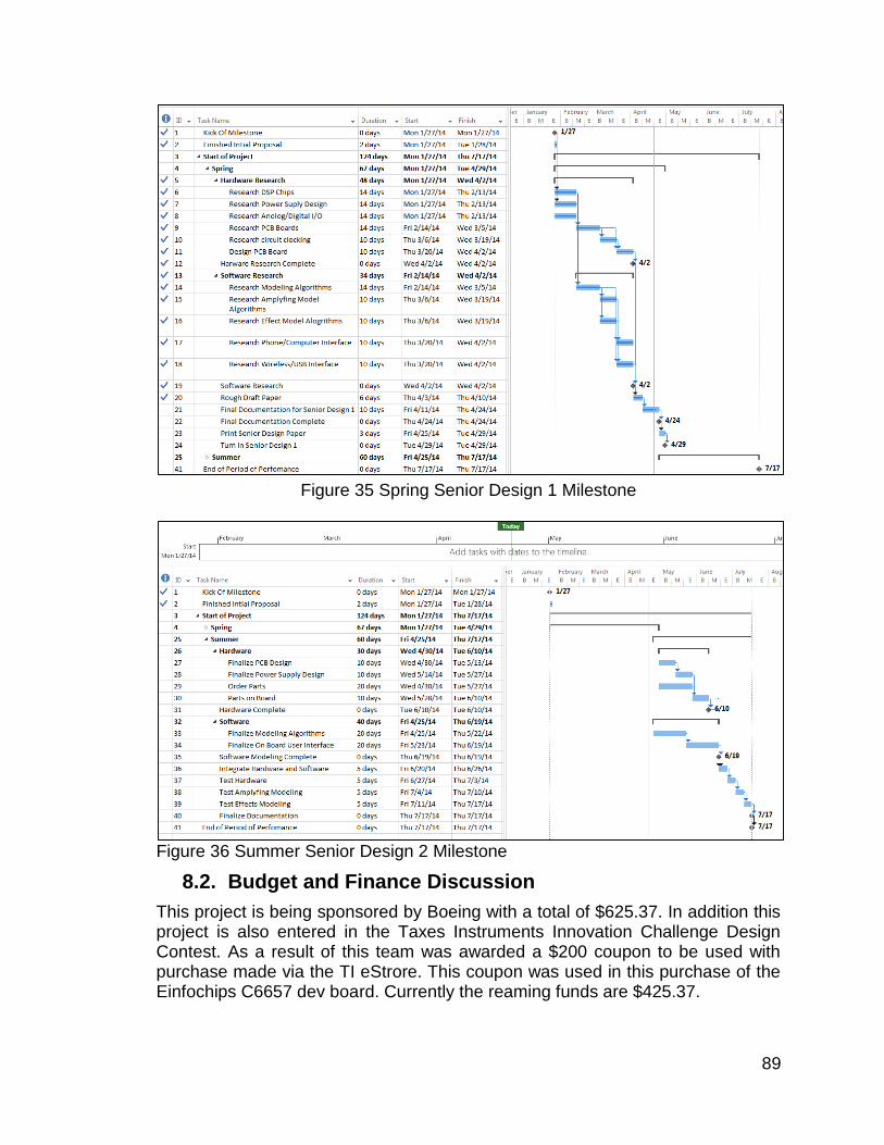
89
Figure 35 Spring Senior Design 1 Milestone
Figure 36 Summer Senior Design 2 Milestone
8.2. Budget and Finance Discussion
This project is being sponsored by Boeing with a total of $625.37. In addition this project is also entered in the Taxes Instruments Innovation Challenge Design Contest. As a result of this team was awarded a $200 coupon to be used with purchase made via the TI eStrore. This coupon was used in this purchase of the Einfochips C6657 dev board. Currently the reaming funds are $425.37.

90
TYPE PART NO Qty Coast Each Total Coast
Regulator
TLV70130 1 $ 0.29 $ 0.29
TPS70930 1 $ 0.29 $ 0.29
LM1086 1 $ 0.76 $ 0.76
LP2985-N 1 $ 0.26 $ 0.26
TPS76850 1 $ 1.10 $ 1.10
TL780-15 1 $ 0.40 $ 0.40
LM320-N 1 $ 0.62 $ 0.62
TPS7A8001 1 $ 1.15 $ 1.15
TPS72515 1 $ 1.35 $ 1.35
TPS725181 1 $ 1.35 $ 1.35
LM21215 1 $ 4.26 $ 4.26
UA7808 1 $ 0.36 $ 0.36
TL780-15 1 $ 0.40 $ 0.40
LM320-N 1 $ 0.62 $ 0.62
LM1084 1 $ 1.65 $ 1.65
Transformer VPT36-4440 1 $ 55.93 $ 55.93
MCU / Logic LM10011 1 $ 0.60 $ 0.60
MSP430G2553IPW28R 2 $ 0.99 $ 1.98
ADC/DAC
PCM4222 1 $ 10.95 $ 10.95
PCM1794A 2 $ 9.22 $ 18.44
Si530 VCXO 1 $ 9.79 $ 9.79
Opamp
NE5534 2 $ 0.54 $ 1.08
LT1028 4 $ 8.75 $ 35.00
OPA827 2 $ 4.50 $ 9.00
Capacitors N/A mult $ 50.00 $ 50.00
Resistors N/A mult $ 50.00 $ 50.00
2U Chassis 546-RMCS19038BK1 1 $ 78.96 $ 78.96
Ouput Amp TPA6120A2 1 $ 2.68 $ 2.68
DRV134 2 $ 1.95 $ 3.90
PCB N/A 3 $ 600.00 $ 600.00
Processor TMS320C6657 1 $ 86.00 $ 86.00
Development board TMS320C6657 Lite EVM 1 $ 400.00 $ 400.00
Display NHD‐24064WG‐ATMI‐VZ# 1 $ 44.94 $ 44.94
Pushbutton 59-111 6 $ 6.33 $ 37.98
Toggle Switch LT-1511-610-012 1 $ 10.55 $ 10.55
Miscellaneous Parts N/A N/A $ 150.00 $ 150.00
Totals $ 1,672.64
Table 31 Budget and Cost

I
9. Appendix A – References
Analog Devices, Inc. 2014. ADSP-BF534/ADSP-BF536/ADSP-BF537. Data
Manual, Analog Devices, Inc. Brown, Marty. 2001. Power Supply Cookbook. Butterworth-Heinemann. Lenk, John D. 1994. Simplified Design of Linear Power Supplies. Butterworth-
Heinemann. Newhaven Display Internation, Inc. 2013. NHD-24064WG-ATMI-VZ#. Datasheet,
Newhaven Display Internation, Inc. Texas Instruments Incorporated. 2007. AC-Coupling Between Differential
LVPECL, LVDS, HSTL, and CML. Application Report, Texas Instruments Incorporated.
Texas Instruments Incorporated. 2010. Clocking Desgn Guide for KeyStone Devices. Application Report, Texas Instruments Incorporated.
Texas Instruments Incorporated. 2013. DDR3 Design Requirements for KeyStone Devices. Application Report, Texas Instruments Incorporated.
Texas Instruments Incorporated. 2011. DDR3 Memory COntroller. User Guide, Texas Instruments Incorporated.
Texas Instruments Incorporated. 2013. DSP Bootloader. User Guide, Texas Instruments Incorporated.
Texas Instruments Incorporated. 2011. External Memory Interface (EMIF16). User Guide, Texas Instruments Incorporated.
Texas Instruments Incorporated. 2010. General Purpose Input/Output (GPIO). User Guide, Texas Instruments Incorporated.
Texas Instruments Incorporated. 2013. Hardware Design Guide for Keystone I Devices. Application Report, Texas Instruments Incorporated.
Texas Instruments Incorporated. 2014. KeyStone I DDR3 Initialization. Application Report, Texas Instruments Incorporated.
Texas Instruments Incorporated. 2013. MSP430G2x53, MSP430G2x13 Mixed Signal Microcontroller. Datasheet, Texas Instruments Incorporated.
Texas Instruments Incorporated. 2012. Multichannel Buffered Serial Port (McBSP). User Guide, Texas Instruments Incorporated.
Texas Instruments Incorporated. 2013. Phase-Locked Loop (PLL). User Guide, Texas Instruments Incorporated.
Texas Instruments Incorporated. 2012. Serial Perpheral Interface (SPI). User Guide, Texas Instruments Incorporated.
Texas Instruments Incorporated. 2012. Serial Rapid IO (SRIO). User Guide, Texas Instruments Incorporated.
Texas Instruments Incorporated. 2014. SYS/BIOS (TI-RTOS Kernel) v6.40. User's Guide, Texas Instruments Incorporated.
Texas Instruments Incorporated. 2014. TMS320C6000 OPtimizing Compiler v7.6. User's Guide, Texas Instruments Incorporated.
Texas Instruments Incorporated. 2010. TMS320C6457. Data Manual, Texas Instruments Incorporated.

II
Texas Instruments Incorporated. 2012. TMS320C6657/57 Fixed and Floating-Point Digital Signal Processor. Data Manual, Texas Instruments Incorporated.
Texas Instruments Incorporated. 2012. TMX320C6657 Evaluation Module Quick Setup Guide. Setup Guide, Texas Instruments Incorporated.
Texas Instruments Incorporated. 2010. Universal Asynchronous Receiver/Transmitter (UART). User Guide, Texas Instruments Incorporated.
Texas Instruments Incorporated. 2012. Universal Parallel Port (uPP). User Guide, Texas Instruments Incorporated.
10. Appendix B – Permissions

III