diagnostic-quality acquisition system for bio-electric
TRANSCRIPT

This is preliminary information on a new product now in development or undergoing evaluation. Details are subject to change without notice.
April 2014 DocID026157 Rev 2 1/85
HM301D
Diagnostic-quality acquisition system for bio-electric sensors and bio-impedance measurements
Datasheet - preliminary data
Features
3 biopotential acquisition channels with integrated analog high pass filters
1 bio-impedance measurement channel with 2- or 4-wire measurement
Digital IQ demodulation
Integrated configurable digital filtering and preprocessing
Pacemaker pulse acquisition with embedded detection function (down to 0.1 mV impulse amplitude)
Input connection matrix allows support for different cable configurations
SPI daisy chain supports up to 4 ICs connection
Programmable analog gain: 8, 16, 32, 64
Low supply voltage: 1.62 V to 3.6 V
Input referred noise: 6 µVPP (300 Hz BW, G=64)
Maximum data rate: 125 kSPS per channel
Less than 1 mA/channel at full bandwidth and resolution
DC and AC lead-off detection
Right leg driver (RLD), Wilson common terminal (WCT) and shield driver (SD)
Clock reconfigurability
Built-in ring oscillator (±5% accuracy)
Built-in crystal oscillator (±0.1% accuracy)
External clock
Low external component count architecture
Allows compliance with medical standards ANSI/AAMI EC11, ANSI/AAMI EC13 and IEC60601-2-27
EMI tolerant
Applications
ECG (electrocardiogram)
Carts for clinical environments
Bedside monitoring
Holter monitors
Automated external defibrillator (AED)
EEG (electroencephalogram)
EMG (electromyography)
Wearable remote monitoring
Medical equipment
LGA 40 L (6 x 6 mm)
Table 1. Device summary
Order codeBiopotential
channelsBio-impedance
channelMarking Package Packaging
HM301DL 3 Yes HM301D LGA 6x6 40L Tray
www.st.com

Contents HM301D
2/85 DocID026157 Rev 2
Contents
1 Description . . . . . . . . . . . . . . . . . . . . . . . . . . . . . . . . . . . . . . . . . . . . . . . . . 7
2 Block diagram . . . . . . . . . . . . . . . . . . . . . . . . . . . . . . . . . . . . . . . . . . . . . . 8
3 Pin configuration . . . . . . . . . . . . . . . . . . . . . . . . . . . . . . . . . . . . . . . . . . . . 9
4 Maximum ratings . . . . . . . . . . . . . . . . . . . . . . . . . . . . . . . . . . . . . . . . . . . 11
5 Electrical characteristics . . . . . . . . . . . . . . . . . . . . . . . . . . . . . . . . . . . . 12
6 Detailed description . . . . . . . . . . . . . . . . . . . . . . . . . . . . . . . . . . . . . . . . 16
6.1 Overview . . . . . . . . . . . . . . . . . . . . . . . . . . . . . . . . . . . . . . . . . . . . . . . . . 16
6.2 Input connection matrix . . . . . . . . . . . . . . . . . . . . . . . . . . . . . . . . . . . . . . 17
6.3 Biopotential channel . . . . . . . . . . . . . . . . . . . . . . . . . . . . . . . . . . . . . . . . . 18
6.3.1 Analog section . . . . . . . . . . . . . . . . . . . . . . . . . . . . . . . . . . . . . . . . . . . . 18
6.3.2 Digital section . . . . . . . . . . . . . . . . . . . . . . . . . . . . . . . . . . . . . . . . . . . . 20
6.3.3 High resolution low bandwidth signal path (HRLB) . . . . . . . . . . . . . . . . 21
6.3.4 Low resolution high bandwidth signal path (LRHB) . . . . . . . . . . . . . . . . 21
6.4 Lead off detection . . . . . . . . . . . . . . . . . . . . . . . . . . . . . . . . . . . . . . . . . . . 22
6.4.1 DC contact check . . . . . . . . . . . . . . . . . . . . . . . . . . . . . . . . . . . . . . . . . . 23
6.4.2 AC contact check . . . . . . . . . . . . . . . . . . . . . . . . . . . . . . . . . . . . . . . . . . 23
6.5 Impedance channel . . . . . . . . . . . . . . . . . . . . . . . . . . . . . . . . . . . . . . . . . 24
6.5.1 Analog section . . . . . . . . . . . . . . . . . . . . . . . . . . . . . . . . . . . . . . . . . . . . 25
6.5.2 Digital section . . . . . . . . . . . . . . . . . . . . . . . . . . . . . . . . . . . . . . . . . . . . 25
6.6 Drivers . . . . . . . . . . . . . . . . . . . . . . . . . . . . . . . . . . . . . . . . . . . . . . . . . . . 26
6.6.1 Right leg driver . . . . . . . . . . . . . . . . . . . . . . . . . . . . . . . . . . . . . . . . . . . . 27
6.6.2 Shield driver . . . . . . . . . . . . . . . . . . . . . . . . . . . . . . . . . . . . . . . . . . . . . . 27
6.6.3 Wilson common terminal (WCT) . . . . . . . . . . . . . . . . . . . . . . . . . . . . . . 27
6.7 TM and RST pin configuration . . . . . . . . . . . . . . . . . . . . . . . . . . . . . . . . . 28
6.8 Digital machine . . . . . . . . . . . . . . . . . . . . . . . . . . . . . . . . . . . . . . . . . . . . . 29
6.8.1 Operating modes . . . . . . . . . . . . . . . . . . . . . . . . . . . . . . . . . . . . . . . . . . 29
6.8.2 Sleep . . . . . . . . . . . . . . . . . . . . . . . . . . . . . . . . . . . . . . . . . . . . . . . . . . . 29
6.8.3 Boot . . . . . . . . . . . . . . . . . . . . . . . . . . . . . . . . . . . . . . . . . . . . . . . . . . . . 29
6.8.4 Standby . . . . . . . . . . . . . . . . . . . . . . . . . . . . . . . . . . . . . . . . . . . . . . . . . 29

DocID026157 Rev 2 3/85
HM301D Contents
85
6.8.5 Ready . . . . . . . . . . . . . . . . . . . . . . . . . . . . . . . . . . . . . . . . . . . . . . . . . . 30
6.8.6 Measure . . . . . . . . . . . . . . . . . . . . . . . . . . . . . . . . . . . . . . . . . . . . . . . . . 30
6.8.7 Fast recovery . . . . . . . . . . . . . . . . . . . . . . . . . . . . . . . . . . . . . . . . . . . . . 31
6.9 GPIO configuration . . . . . . . . . . . . . . . . . . . . . . . . . . . . . . . . . . . . . . . . . . 32
6.10 SPI interface . . . . . . . . . . . . . . . . . . . . . . . . . . . . . . . . . . . . . . . . . . . . . . . 36
6.10.1 SPI read . . . . . . . . . . . . . . . . . . . . . . . . . . . . . . . . . . . . . . . . . . . . . . . . . 36
6.10.2 SPI write . . . . . . . . . . . . . . . . . . . . . . . . . . . . . . . . . . . . . . . . . . . . . . . . 37
6.10.3 Daisy chain SPI . . . . . . . . . . . . . . . . . . . . . . . . . . . . . . . . . . . . . . . . . . . 38
6.10.4 SPI timing . . . . . . . . . . . . . . . . . . . . . . . . . . . . . . . . . . . . . . . . . . . . . . . 41
6.11 Power supply voltage monitor . . . . . . . . . . . . . . . . . . . . . . . . . . . . . . . . . 42
6.12 Registers MAP . . . . . . . . . . . . . . . . . . . . . . . . . . . . . . . . . . . . . . . . . . . . . 42
6.12.1 Application settings (Read/Write) . . . . . . . . . . . . . . . . . . . . . . . . . . . . . . 46
6.12.2 Output flags (read only) . . . . . . . . . . . . . . . . . . . . . . . . . . . . . . . . . . . . . 60
6.12.3 Data registers (readable only if MEAS_MODE = 1) . . . . . . . . . . . . . . . . 61
6.13 Output data format . . . . . . . . . . . . . . . . . . . . . . . . . . . . . . . . . . . . . . . . . . 69
6.13.1 Case 1: complete processed data - 4x packet . . . . . . . . . . . . . . . . . . . . 70
6.13.2 Case 2: pre-filtered data out - 3x packet . . . . . . . . . . . . . . . . . . . . . . . . 71
6.13.3 Header description . . . . . . . . . . . . . . . . . . . . . . . . . . . . . . . . . . . . . . . . . 72
6.14 Data rate . . . . . . . . . . . . . . . . . . . . . . . . . . . . . . . . . . . . . . . . . . . . . . . . . . 74
6.15 Data ready operation . . . . . . . . . . . . . . . . . . . . . . . . . . . . . . . . . . . . . . . . 75
7 Application Information . . . . . . . . . . . . . . . . . . . . . . . . . . . . . . . . . . . . . 77
7.1 DC offset removal . . . . . . . . . . . . . . . . . . . . . . . . . . . . . . . . . . . . . . . . . . . 77
7.2 Multi-chip configuration . . . . . . . . . . . . . . . . . . . . . . . . . . . . . . . . . . . . . . 78
7.3 Supported ECG configurations . . . . . . . . . . . . . . . . . . . . . . . . . . . . . . . . . 80
8 Package mechanical data . . . . . . . . . . . . . . . . . . . . . . . . . . . . . . . . . . . . 81
9 Revision history . . . . . . . . . . . . . . . . . . . . . . . . . . . . . . . . . . . . . . . . . . . 84

List of tables HM301D
4/85 DocID026157 Rev 2
List of tables
Table 1. Device summary . . . . . . . . . . . . . . . . . . . . . . . . . . . . . . . . . . . . . . . . . . . . . . . . . . . . . . . . . . 1Table 2. Pin description . . . . . . . . . . . . . . . . . . . . . . . . . . . . . . . . . . . . . . . . . . . . . . . . . . . . . . . . . . . 9Table 3. Absolute maximum ratings . . . . . . . . . . . . . . . . . . . . . . . . . . . . . . . . . . . . . . . . . . . . . . . . . 11Table 4. Thermal data. . . . . . . . . . . . . . . . . . . . . . . . . . . . . . . . . . . . . . . . . . . . . . . . . . . . . . . . . . . . 11Table 5. Electrical characteristics . . . . . . . . . . . . . . . . . . . . . . . . . . . . . . . . . . . . . . . . . . . . . . . . . . . 12Table 6. Input-referred noise (µVRMS/µVPP) / 3 V analog supply 1 . . . . . . . . . . . . . . . . . . . . . . . . . 15Table 7. Input connection matrix. . . . . . . . . . . . . . . . . . . . . . . . . . . . . . . . . . . . . . . . . . . . . . . . . . . . 17Table 8. Pad connection settings . . . . . . . . . . . . . . . . . . . . . . . . . . . . . . . . . . . . . . . . . . . . . . . . . . . 18Table 9. Biopotential channel gain and IDR . . . . . . . . . . . . . . . . . . . . . . . . . . . . . . . . . . . . . . . . . . . 19Table 10. Functional modes . . . . . . . . . . . . . . . . . . . . . . . . . . . . . . . . . . . . . . . . . . . . . . . . . . . . . . . . 29Table 11. Digital GPIO output signals (DGIO0) . . . . . . . . . . . . . . . . . . . . . . . . . . . . . . . . . . . . . . . . . 32Table 12. Digital GPIO output signals (DGIO1) . . . . . . . . . . . . . . . . . . . . . . . . . . . . . . . . . . . . . . . . . 32Table 13. Digital GPIO output signals (DGIO2) . . . . . . . . . . . . . . . . . . . . . . . . . . . . . . . . . . . . . . . . . 34Table 14. Digital GPIO input signals . . . . . . . . . . . . . . . . . . . . . . . . . . . . . . . . . . . . . . . . . . . . . . . . . . 36Table 15. Read command bytes. . . . . . . . . . . . . . . . . . . . . . . . . . . . . . . . . . . . . . . . . . . . . . . . . . . . . 37Table 16. Write command byte. . . . . . . . . . . . . . . . . . . . . . . . . . . . . . . . . . . . . . . . . . . . . . . . . . . . . . 38Table 17. SPI slave timings (IOVDD = 1.8 V) . . . . . . . . . . . . . . . . . . . . . . . . . . . . . . . . . . . . . . . . . . . 41Table 18. Psmon_out signal . . . . . . . . . . . . . . . . . . . . . . . . . . . . . . . . . . . . . . . . . . . . . . . . . . . . . . . . 42Table 19. Registers MAP . . . . . . . . . . . . . . . . . . . . . . . . . . . . . . . . . . . . . . . . . . . . . . . . . . . . . . . . . . 42Table 20. Registers MAP . . . . . . . . . . . . . . . . . . . . . . . . . . . . . . . . . . . . . . . . . . . . . . . . . . . . . . . . . . 44Table 21. Data registers (readable only if meas_mode bit is 1) . . . . . . . . . . . . . . . . . . . . . . . . . . . . . 44Table 22. SET0 CH_ENABLE (ADDR 27h) . . . . . . . . . . . . . . . . . . . . . . . . . . . . . . . . . . . . . . . . . . . . 46Table 23. SET1 PM_SEL (ADDR 28h) . . . . . . . . . . . . . . . . . . . . . . . . . . . . . . . . . . . . . . . . . . . . . . . . 46Table 24. SET 2 AVG_CTRL (ADDR 29h) . . . . . . . . . . . . . . . . . . . . . . . . . . . . . . . . . . . . . . . . . . . . . 47Table 25. SET3 INCON_HCSEL_1 (2Ah) . . . . . . . . . . . . . . . . . . . . . . . . . . . . . . . . . . . . . . . . . . . . . 47Table 26. SET4 INCON_HCSEL_2 (2Bh) . . . . . . . . . . . . . . . . . . . . . . . . . . . . . . . . . . . . . . . . . . . . . 47Table 27. SET5 INCON_HCSEL_3 (2Ch) . . . . . . . . . . . . . . . . . . . . . . . . . . . . . . . . . . . . . . . . . . . . . 48Table 28. SET6 INCON_AVG_1 (2Dh). . . . . . . . . . . . . . . . . . . . . . . . . . . . . . . . . . . . . . . . . . . . . . . . 48Table 29. SET7 INCON_AVG_2 (2Eh) . . . . . . . . . . . . . . . . . . . . . . . . . . . . . . . . . . . . . . . . . . . . . . . . 49Table 30. SET8 INCON_RLD (2Fh) . . . . . . . . . . . . . . . . . . . . . . . . . . . . . . . . . . . . . . . . . . . . . . . . . . 49Table 31. SET9 CCK_EN_1 (30h) . . . . . . . . . . . . . . . . . . . . . . . . . . . . . . . . . . . . . . . . . . . . . . . . . . . 50Table 32. SET10 CCK_EN_2 (31h) . . . . . . . . . . . . . . . . . . . . . . . . . . . . . . . . . . . . . . . . . . . . . . . . . . 50Table 33. SET11 CCK_CUR (32h) . . . . . . . . . . . . . . . . . . . . . . . . . . . . . . . . . . . . . . . . . . . . . . . . . . . 51Table 34. SET12 CCK_TRSH (33h) . . . . . . . . . . . . . . . . . . . . . . . . . . . . . . . . . . . . . . . . . . . . . . . . . . 52Table 35. SET13 HC_ANA_CTRL (34h) . . . . . . . . . . . . . . . . . . . . . . . . . . . . . . . . . . . . . . . . . . . . . . 53Table 36. SET14 IMP_ANA_CTRL (35h) . . . . . . . . . . . . . . . . . . . . . . . . . . . . . . . . . . . . . . . . . . . . . . 53Table 37. SET15 ECG_DIGFILT_CTRL (36h) . . . . . . . . . . . . . . . . . . . . . . . . . . . . . . . . . . . . . . . . . . 54Table 38. SET16 PM_DIGFILT_CTRL (37h) . . . . . . . . . . . . . . . . . . . . . . . . . . . . . . . . . . . . . . . . . . . 54Table 39. SET17 HC_DIGFILT_CTRL (38h) . . . . . . . . . . . . . . . . . . . . . . . . . . . . . . . . . . . . . . . . . . . 55Table 40. SET18 HC_HPFANA_CTRL (39h) . . . . . . . . . . . . . . . . . . . . . . . . . . . . . . . . . . . . . . . . . . . 55Table 41. SET19 RLD_CTRL (3Ah) . . . . . . . . . . . . . . . . . . . . . . . . . . . . . . . . . . . . . . . . . . . . . . . . . . 56Table 42. SET20 RECOVERY_TIME (3Bh) . . . . . . . . . . . . . . . . . . . . . . . . . . . . . . . . . . . . . . . . . . . . 57Table 43. SET21 PMD_TRSH (3Ch) . . . . . . . . . . . . . . . . . . . . . . . . . . . . . . . . . . . . . . . . . . . . . . . . . 57Table 44. SET22 FILTER_SWTIME (3Dh) . . . . . . . . . . . . . . . . . . . . . . . . . . . . . . . . . . . . . . . . . . . . . 58Table 45. SET23 DIGIO_IO (40h) . . . . . . . . . . . . . . . . . . . . . . . . . . . . . . . . . . . . . . . . . . . . . . . . . . . 58Table 46. SET24 IMP_CUR_EN (44h) . . . . . . . . . . . . . . . . . . . . . . . . . . . . . . . . . . . . . . . . . . . . . . . . 58Table 47. SET25 DIGIO12_SEL (45h) . . . . . . . . . . . . . . . . . . . . . . . . . . . . . . . . . . . . . . . . . . . . . . . . 59Table 48. SET26 DIGIO0_SEL (46h) . . . . . . . . . . . . . . . . . . . . . . . . . . . . . . . . . . . . . . . . . . . . . . . . . 59

DocID026157 Rev 2 5/85
HM301D List of tables
85
Table 49. OUT_FLAG0 (47h) . . . . . . . . . . . . . . . . . . . . . . . . . . . . . . . . . . . . . . . . . . . . . . . . . . . . . . . 60Table 50. OUT_FLAG1 (48h) . . . . . . . . . . . . . . . . . . . . . . . . . . . . . . . . . . . . . . . . . . . . . . . . . . . . . . . 60Table 51. ECG1_DATAOUT_1 (49h) . . . . . . . . . . . . . . . . . . . . . . . . . . . . . . . . . . . . . . . . . . . . . . . . . 61Table 52. CG1_DATAOUT_0 (4Ah) . . . . . . . . . . . . . . . . . . . . . . . . . . . . . . . . . . . . . . . . . . . . . . . . . . 61Table 53. ECG2_DATAOUT_1 (4Bh) . . . . . . . . . . . . . . . . . . . . . . . . . . . . . . . . . . . . . . . . . . . . . . . . . 61Table 54. ECG2_DATAOUT_0 (4Ch) . . . . . . . . . . . . . . . . . . . . . . . . . . . . . . . . . . . . . . . . . . . . . . . . . 62Table 55. ECG3_DATAOUT_1 (4Dh) . . . . . . . . . . . . . . . . . . . . . . . . . . . . . . . . . . . . . . . . . . . . . . . . . 62Table 56. ECG3_DATAOUT_0 (4Eh) . . . . . . . . . . . . . . . . . . . . . . . . . . . . . . . . . . . . . . . . . . . . . . . . . 62Table 57. ECG12_DATAOUT_1 (4Fh) . . . . . . . . . . . . . . . . . . . . . . . . . . . . . . . . . . . . . . . . . . . . . . . . 63Table 58. ECG12_DATAOUT_0 (50h) . . . . . . . . . . . . . . . . . . . . . . . . . . . . . . . . . . . . . . . . . . . . . . . . 63Table 59. ECG23_DATAOUT_1 (51h) . . . . . . . . . . . . . . . . . . . . . . . . . . . . . . . . . . . . . . . . . . . . . . . . 63Table 60. ECG23_DATAOUT_0 (52h) . . . . . . . . . . . . . . . . . . . . . . . . . . . . . . . . . . . . . . . . . . . . . . . . 64Table 61. ECG31_DATAOUT_1 (53h) . . . . . . . . . . . . . . . . . . . . . . . . . . . . . . . . . . . . . . . . . . . . . . . . 64Table 62. ECG31_DATAOUT_0 (54h) . . . . . . . . . . . . . . . . . . . . . . . . . . . . . . . . . . . . . . . . . . . . . . . . 64Table 63. PM1_DATAOUT_1 (55h) . . . . . . . . . . . . . . . . . . . . . . . . . . . . . . . . . . . . . . . . . . . . . . . . . . 65Table 64. PM1_DATAOUT_0 (56h) . . . . . . . . . . . . . . . . . . . . . . . . . . . . . . . . . . . . . . . . . . . . . . . . . . 65Table 65. PM2_DATAOUT_1 (57h) . . . . . . . . . . . . . . . . . . . . . . . . . . . . . . . . . . . . . . . . . . . . . . . . . . 65Table 66. PM2_DATAOUT_0 (58h) . . . . . . . . . . . . . . . . . . . . . . . . . . . . . . . . . . . . . . . . . . . . . . . . . . 66Table 67. IMPEDANCE_PHASE_AC_DATAOUT_1 (59h). . . . . . . . . . . . . . . . . . . . . . . . . . . . . . . . . 66Table 68. IMPEDANCE_PHASE_AC_DATAOUT_0 (5Ah) . . . . . . . . . . . . . . . . . . . . . . . . . . . . . . . . 66Table 69. IMPEDANCE_SQUARING_AC_DATAOUT_1 (5Bh) . . . . . . . . . . . . . . . . . . . . . . . . . . . . . 67Table 70. IMPEDANCE_SQUARING_AC_DATAOUT_0 (5Ch) . . . . . . . . . . . . . . . . . . . . . . . . . . . . . 67Table 71. IMPEDANCE_PHASE_DC_DATAOUT_1 (5Dh) . . . . . . . . . . . . . . . . . . . . . . . . . . . . . . . . 67Table 72. IMPEDANCE_PHASE_DC_DATAOUT_0 (5Eh) . . . . . . . . . . . . . . . . . . . . . . . . . . . . . . . . 68Table 73. IMPEDANCE_SQUARING_DC_DATAOUT_1 (5Fh) . . . . . . . . . . . . . . . . . . . . . . . . . . . . . 68Table 74. IMPEDANCE_SQUARING_DC_DATAOUT_0 (60h) . . . . . . . . . . . . . . . . . . . . . . . . . . . . . 68Table 75. CONTACT_CHECK_DATAOUT_1 (61h) . . . . . . . . . . . . . . . . . . . . . . . . . . . . . . . . . . . . . . 69Table 76. CONTACT_CHECK_DATAOUT_0 (62h) . . . . . . . . . . . . . . . . . . . . . . . . . . . . . . . . . . . . . . 69Table 77. Data format . . . . . . . . . . . . . . . . . . . . . . . . . . . . . . . . . . . . . . . . . . . . . . . . . . . . . . . . . . . . . 70Table 78. Base pocket . . . . . . . . . . . . . . . . . . . . . . . . . . . . . . . . . . . . . . . . . . . . . . . . . . . . . . . . . . . . 70Table 79. Data packet out with 3 HM301D in chain . . . . . . . . . . . . . . . . . . . . . . . . . . . . . . . . . . . . . . 70Table 80. Pre-filtered data out . . . . . . . . . . . . . . . . . . . . . . . . . . . . . . . . . . . . . . . . . . . . . . . . . . . . . . 71Table 81. Header packet bits description in 4x packet case. . . . . . . . . . . . . . . . . . . . . . . . . . . . . . . . 72Table 82. Header packet bits description in 3x packet case. . . . . . . . . . . . . . . . . . . . . . . . . . . . . . . . 72Table 83. C_DATA packet description bits configurations . . . . . . . . . . . . . . . . . . . . . . . . . . . . . . . . . 73Table 84. Contact check and overflow C_DATA vector . . . . . . . . . . . . . . . . . . . . . . . . . . . . . . . . . . . 74Table 85. HRLB data-out sampling frequency vs low pass filter cut-off frequency. . . . . . . . . . . . . . . 74Table 86. LRHB data-out sampling frequency vs low pass filter cut-off frequency. . . . . . . . . . . . . . . 75Table 87. Impedance data-out sampling frequency vs low pass filter cut-off frequency. . . . . . . . . . . 75Table 88. Common ECG configurations . . . . . . . . . . . . . . . . . . . . . . . . . . . . . . . . . . . . . . . . . . . . . . . 80Table 89. LGA 40L (6 x 6 mm) mechanical data . . . . . . . . . . . . . . . . . . . . . . . . . . . . . . . . . . . . . . . . 83Table 90. Document revision history . . . . . . . . . . . . . . . . . . . . . . . . . . . . . . . . . . . . . . . . . . . . . . . . . 84
List of figures HM301D
6/85 DocID026157 Rev 2
List of figures
Figure 1. HM301D block diagram . . . . . . . . . . . . . . . . . . . . . . . . . . . . . . . . . . . . . . . . . . . . . . . . . . . . 8Figure 2. Pin configuration (top view) . . . . . . . . . . . . . . . . . . . . . . . . . . . . . . . . . . . . . . . . . . . . . . . . . 9Figure 3. Biopotential channel block schematic . . . . . . . . . . . . . . . . . . . . . . . . . . . . . . . . . . . . . . . . . 18Figure 4. First decimation filter. . . . . . . . . . . . . . . . . . . . . . . . . . . . . . . . . . . . . . . . . . . . . . . . . . . . . . 20Figure 5. HRLB digital signal path . . . . . . . . . . . . . . . . . . . . . . . . . . . . . . . . . . . . . . . . . . . . . . . . . . . 21Figure 6. LRHB signal path . . . . . . . . . . . . . . . . . . . . . . . . . . . . . . . . . . . . . . . . . . . . . . . . . . . . . . . . 22Figure 7. Contact check architecture . . . . . . . . . . . . . . . . . . . . . . . . . . . . . . . . . . . . . . . . . . . . . . . . . 23Figure 8. Impedance channel architecture. . . . . . . . . . . . . . . . . . . . . . . . . . . . . . . . . . . . . . . . . . . . . 24Figure 9. Impedance channel digital section . . . . . . . . . . . . . . . . . . . . . . . . . . . . . . . . . . . . . . . . . . . 26Figure 10. AVG buffers . . . . . . . . . . . . . . . . . . . . . . . . . . . . . . . . . . . . . . . . . . . . . . . . . . . . . . . . . . . . 27Figure 11. WCT buffer . . . . . . . . . . . . . . . . . . . . . . . . . . . . . . . . . . . . . . . . . . . . . . . . . . . . . . . . . . . . . 28Figure 12. State machine for packets streaming mode (meas_mode = 0) . . . . . . . . . . . . . . . . . . . . . 30Figure 13. State machine for packets streaming mode (meas_mode = 1) . . . . . . . . . . . . . . . . . . . . . 31Figure 14. Single byte reading . . . . . . . . . . . . . . . . . . . . . . . . . . . . . . . . . . . . . . . . . . . . . . . . . . . . . . . 37Figure 15. Double byte reading . . . . . . . . . . . . . . . . . . . . . . . . . . . . . . . . . . . . . . . . . . . . . . . . . . . . . . 37Figure 16. Single byte writing. . . . . . . . . . . . . . . . . . . . . . . . . . . . . . . . . . . . . . . . . . . . . . . . . . . . . . . . 38Figure 17. Example of daisy chain SPI connection with 3 HM301D . . . . . . . . . . . . . . . . . . . . . . . . . . 38Figure 18. Example of daisy chain SPI writing. . . . . . . . . . . . . . . . . . . . . . . . . . . . . . . . . . . . . . . . . . . 39Figure 19. Example of daisy chain SPI reading . . . . . . . . . . . . . . . . . . . . . . . . . . . . . . . . . . . . . . . . . . 40Figure 20. SPI timing . . . . . . . . . . . . . . . . . . . . . . . . . . . . . . . . . . . . . . . . . . . . . . . . . . . . . . . . . . . . . . 41Figure 21. SPI communication - packet data streaming . . . . . . . . . . . . . . . . . . . . . . . . . . . . . . . . . . . 75Figure 22. ECG_OUT registers data reading. . . . . . . . . . . . . . . . . . . . . . . . . . . . . . . . . . . . . . . . . . . . 76Figure 23. Maximum DC offset removal . . . . . . . . . . . . . . . . . . . . . . . . . . . . . . . . . . . . . . . . . . . . . . . 78Figure 24. Example of chain connection: standard 12-lead ECG . . . . . . . . . . . . . . . . . . . . . . . . . . . . 79Figure 25. Package outline for LGA 40L (6 x 6 mm) . . . . . . . . . . . . . . . . . . . . . . . . . . . . . . . . . . . . . . 82

DocID026157 Rev 2 7/85
HM301D Description
85
1 Description
The HM301D is a highly integrated diagnostic-quality biopotential acquisition system with 3 differential channels. Multi master/slave configuration supports up to 16 channels of simultaneous sampling (12 biopotential acquisitions and 4 bio-impedance channels). A fully integrated high-pass filter removes the half-cell DC value to enable the channels to work with the AC component only. Each channel provides high resolution and low noise conversion of biopotential signals up to 10 kHz.
The input connection circuit matrix guarantees maximum flexibility in terms of electrode cables and connectors.
The HM301D includes a dedicated impedance measurement channel that can be used to measure both body impedance average value and variation due to respiration. This channel delivers both the real and the imaginary parts of the body and the breathing impedances. The WCT circuit and driver block implements the driving functions (right leg driver and shield driver) and the Wilson common terminal commonly used in ECG systems.
The electrode-to-skin contact is checked by injecting an AC or DC current. A digital filtering and preprocessing (DFP) block implements configurable band-pass filters, IQ impedance demodulation and enables specific algorithm implementation for lead-off check and pacemaker detection.
The SPI interface allows the exchange of data with both the microcontroller and other HM301D devices in case of chain connection. Full configurability and low power design techniques make it ideal for many applications, including battery-powered devices. High quality recordings are obtained with a small, power-saving system. The 3-channel version is available in a 6 x 6 mm 40-lead LGA.

Block diagram HM301D
8/85 DocID026157 Rev 2
2 Block diagram
Figure 1. HM301D block diagram
Input
Mat r i x
Bi o Pot ent i a l CH3
Chop Amplifier+ADC
DC&AC Contact Check
DRI VERSRLD_COMP
WCT
SD
VSS VSS SGNDSGND AVGIO
XTALIN
XTALOUT
CKEXT
DVSS
CS
SPC
SDI
SDO
VREF
CLOCK
DGIO0
DGIO1
DGIO2
TM1
TM0
NVM
SPI
CONFI G
RST
RLD
VREF
IN3N
IN3P
VREF
IN2P
IN2N
VREF
IN1P
IN1N
Bi o Pot ent i a l CH2
Chop Amplifier+ADC
DC&AC Contact Check
Bi o Pot ent i a l CH1
Chop Amplifier+ADC
DC&AC Contact Check
I mpedanc eChannel
Connec t i on
CIP
CIN
SUPPLYMONI TOR
Imp. ChannelCurrent
Injection FiltersDigital
REFERENCE
VOLTAGE
POR
&
RESET
Dig FiltersLow BW
High RESHRLB
Dig FiltersLow BW
High RESHRLB
Dig FiltersLow BW
High RESHRLB
High BWLowRES
Dig Filters
Dig FiltersHigh BWLowRES
MU
X
AN
A2_
OU
T
AN
A3_
OU
T
AN
A1_
OU
T
VD
D
VD
D
IOV
DD
DV
DD
TEST0
TEST
MUX
AM17580v2

DocID026157 Rev 2 9/85
HM301D Pin configuration
85
3 Pin configuration
Figure 2. Pin configuration (top view)
1
2
3
4
5
6
7
8
9
10
30
29
28
27
26
25
24
23
22
21
11 12 13 14 15 16 17 18 19 20
40 39 38 37 36 35 34 33 32 31
Table 2. Pin description
Pin name Pin n° Type Description
IN1P 1 ANA IN Connected to biopotential channel #1 positive input by default. See input connection matrix to change it
IN1N 2 ANA IN Connected to biopotential channel #1 negative input by default. See input connection matrix to change it
VDD 3 ANA IN Analog supply voltage
IN2P 4 ANA IN Connected to biopotential channel #2 positive input by default. See input connection matrix to change it
IN2N 5 ANA IN Connected to biopotential channel #2 negative input by default. See input connection matrix to change it
VSS 6 ANA GND Analog ground
IN3P 7 ANA IN Connected to biopotential channel #3 positive input by default. See input connection matrix to change it
IN3N 8 ANA IN Connected to biopotential channel #3 negative input by default. See input connection matrix to change it
RLD 9 ANA OUT Connected to Right Leg Driver output by default. See input connection matrix to change it
WCT 10 ANA OUT Wilson Common Terminal output
RLD_COMP 11 ANA IO Input of RLD buffer. To be used for compensation in case of instability of RLD loop

Pin configuration HM301D
10/85 DocID026157 Rev 2
AVGIO 12 ANA IO Average value of electrode signals connected to ASSP (O) or coming from other chain connected ASSPs (I)
SD 13 ANA OUT Driver output of shield cables
ANA1_OUT 14 ANA OUT Channel1 single ended analog output
ANA2_OUT 15 ANA OUT Channel2 single ended analog output
ANA3_OUT 16 ANA OUT Channel3 single ended analog output
TEST0 17 ANA IO Used for TEST purposes. Leave float in normal operation
VSS 18 ANA GND Analog ground
VDD 19 ANA IN Analog supply voltage
VREF 20 ANA IO Reference voltage to or from other chain connected ASSPs
XTALOUT 21 ANA OUT Crystal pin connection
XTALIN 22 ANA IN Crystal pin connection
SGND 23 ANA GND Analog ground
DVDD 24 ANA IN Digital supply voltage
CKEXT 25 DIG IO Clock signal to/from other devices
RST 26DIG OUT POR (when TM0 = TM1 = 0)
DIG IN Enable (when TM0 = 1, TM1 = 0)
TM0 27 DIG IN Configuration pin # 1
TM1 28 DIG IN Configuration pin # 2
DVSS 29 DIG GND Digital ground
SDO 30 DIG OUT SPI Serial Data Output
IOVDD 31 ANA IN Supply voltage for IO pins. It provides the voltage to SPI and GPIOs it must be always lower than VDD.
SDI 32 DIG IN SPI Serial Data Input
CS 33 DIG IN SPI Chip Select
SPC 34 DIG IN SPI Serial Port Clock
DGIO2 35 DIG IO General purpose digital IO
DGIO1 36 DIG IO General purpose digital IO
DGIO0 37 DIG IO General purpose digital IO
SGND 38 ANA GND Analog ground
CIN 39 ANA OUT AC Current Injection Negative pin for Impedance Measurement
CIP 40 ANA OUT AC Current Injection Positive pin for Impedance Measurement
Table 2. Pin description (continued)
Pin name Pin n° Type Description
DocID026157 Rev 2 11/85
HM301D Maximum ratings
85
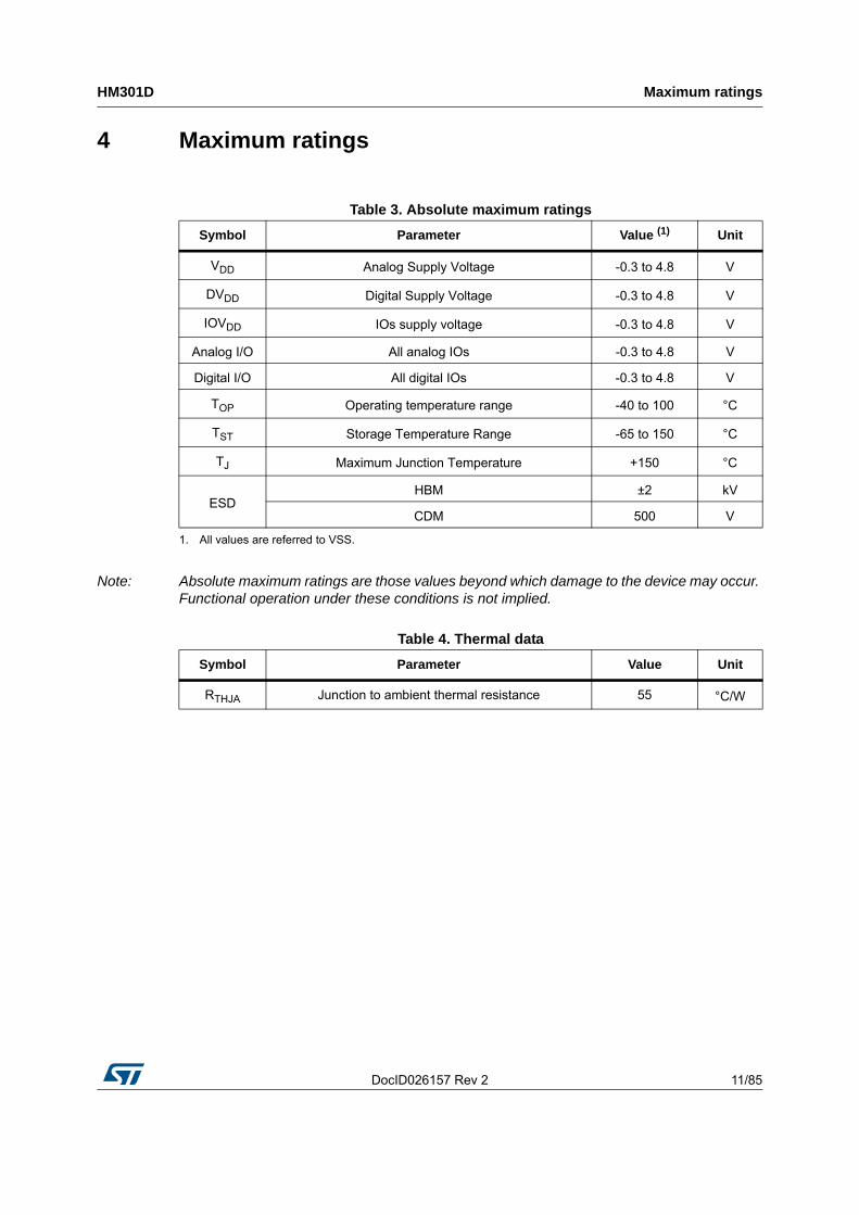
4 Maximum ratings
Note: Absolute maximum ratings are those values beyond which damage to the device may occur. Functional operation under these conditions is not implied.
Table 3. Absolute maximum ratings
Symbol Parameter Value (1)
1. All values are referred to VSS.
Unit
VDD Analog Supply Voltage -0.3 to 4.8 V
DVDD Digital Supply Voltage -0.3 to 4.8 V
IOVDD IOs supply voltage -0.3 to 4.8 V
Analog I/O All analog IOs -0.3 to 4.8 V
Digital I/O All digital IOs -0.3 to 4.8 V
TOP Operating temperature range -40 to 100 °C
TST Storage Temperature Range -65 to 150 °C
TJ Maximum Junction Temperature +150 °C
ESDHBM ±2 kV
CDM 500 V
Table 4. Thermal data
Symbol Parameter Value Unit
RTHJA Junction to ambient thermal resistance 55 °C/W
Electrical characteristics HM301D
12/85 DocID026157 Rev 2
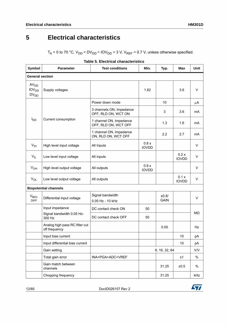
5 Electrical characteristics
TA = 0 to 70 °C, VDD = DVDD = IOVDD = 3 V, VREF = 0.7 V, unless otherwise specified.
Table 5. Electrical characteristics
Symbol Parameter Test conditions Min. Typ. Max Unit
General section
AVDD
IOVDD
DVDD
Supply voltages 1.62 3.6 V
IDD Current consumption
Power down mode 10 A
3 channels ON, Impedance OFF, RLD ON, WCT ON
3 3.6 mA
1 channel ON, Impedance OFF, RLD ON, WCT OFF
1.3 1.6 mA
1 channel ON, Impedance ON, RLD ON, WCT OFF
2.2 2.7 mA
VIH High level input voltage All Inputs0.8 x
IOVDDV
VIL Low level input voltage All inputs0.2 x
IOVDDV
VOH High level output voltage All outputs0.9 x
IOVDDV
VOL Low level output voltage All outputs0.1 x
IOVDDV
Biopotential channels
VBIO-DIFF
Differential input voltageSignal bandwidth
0.05 Hz - 10 kHz
±0.8/ GAIN
V
Input impedance
Signal bandwidth 0.05 Hz-300 Hz
DC contact check ON 50MΩ
DC contact check OFF 50
Analog high pass RC filter cut off frequency
0.05 Hz
Input bias current 10 pA
Input differential bias current 10 pA
Gain setting 8, 16, 32, 64 V/V
Total gain error INA+PGA+ADC+VREF ±1 %
Gain match between channels
31.25 ±0.5 %
Chopping frequency 31.25 kHz
DocID026157 Rev 2 13/85
HM301D Electrical characteristics
85
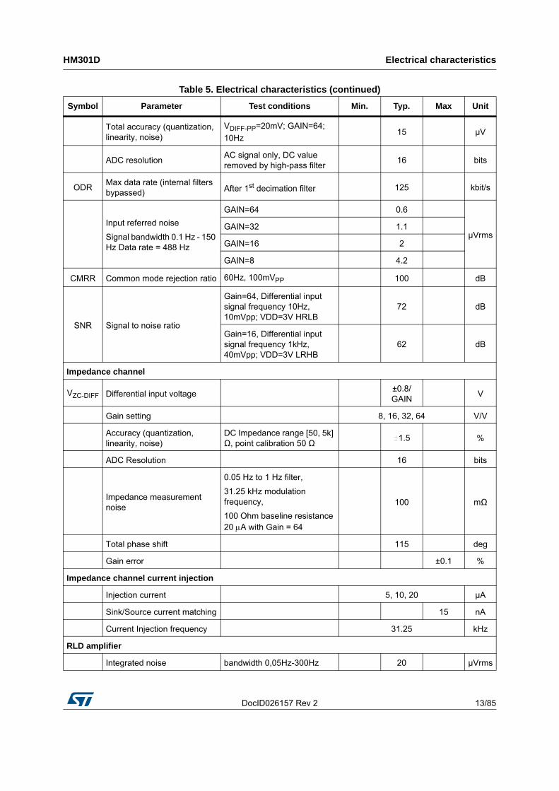
Total accuracy (quantization, linearity, noise)
VDIFF-PP=20mV; GAIN=64;
10Hz15 µV
ADC resolutionAC signal only, DC value removed by high-pass filter
16 bits
ODRMax data rate (internal filters bypassed) After 1st decimation filter 125 kbit/s
Input referred noise
Signal bandwidth 0.1 Hz - 150 Hz Data rate = 488 Hz
GAIN=64 0.6
µVrmsGAIN=32 1.1
GAIN=16 2
GAIN=8 4.2
CMRR Common mode rejection ratio 60Hz, 100mVPP 100 dB
SNR Signal to noise ratio
Gain=64, Differential input signal frequency 10Hz, 10mVpp; VDD=3V HRLB
72 dB
Gain=16, Differential input signal frequency 1kHz, 40mVpp; VDD=3V LRHB
62 dB
Impedance channel
VZC-DIFF Differential input voltage±0.8/ GAIN
V
Gain setting 8, 16, 32, 64 V/V
Accuracy (quantization, linearity, noise)
DC Impedance range [50, 5k] Ω, point calibration 50 Ω
1.5 %
ADC Resolution 16 bits
Impedance measurement noise
0.05 Hz to 1 Hz filter,
31.25 kHz modulation frequency,
100 Ohm baseline resistance 20 A with Gain = 64
100 mΩ
Total phase shift 115 deg
Gain error ±0.1 %
Impedance channel current injection
Injection current 5, 10, 20 µA
Sink/Source current matching 15 nA
Current Injection frequency 31.25 kHz
RLD amplifier
Integrated noise bandwidth 0,05Hz-300Hz 20 µVrms
Table 5. Electrical characteristics (continued)
Symbol Parameter Test conditions Min. Typ. Max Unit

Electrical characteristics HM301D
14/85 DocID026157 Rev 2
Gain f=50Hz 50 dB
Output voltage swing ILIM 880 nAVSS+
0.325VDD-0.35 V
Sink/Source current VDD = 3V 11 µA
Current consumption 90 µA
WCT amplifier
Integrated noise bandwidth 0,05Hz-300Hz 1.5 µVrms
Gain bandwidth product 0.5 MHz
Gain 1 V/V
Sink/Source current 33/18 µA
Output voltage swing VDD=1.8V VREF-0.5VREF+
0.5V
Shield amplifier
Integrated Noise bandwidth 0.05Hz-300Hz 8 µVrms
Gain 1 V/V
Bandwidth 490 Hz
Sink/Source current 10 µA
Output Voltage Swing High Level, VDD=1.8VVREF-
0.63
VREF+
0.59V
Current consumption 11 µA
DC contact check
DC Current 25, 50, 100, 200 nA
DC current accuracy TA=25°C ±5 %
Comparator threshold TA=25°C VSS + 102
VDD- 102
mV
Step threshold 102 mV
AC contact check
Injection current 5, 10, 20 µA
Sink/Source current matching nA
Current Injection frequency See hc_curinj_freq bit 2.5, 5 kHz
Voltage reference
VREF Reference voltage VDD=3.3V; psmon_sel_r=1 1.0 V
Accuracy1 point temperature calibration; TA =25°C ±0.15 %
Table 5. Electrical characteristics (continued)
Symbol Parameter Test conditions Min. Typ. Max Unit

DocID026157 Rev 2 15/85
HM301D Electrical characteristics
85
Integrated noise bandwidth 0.05Hz-300Hz 15 µVrms
Ring oscillator
Frequency 2.00 MHz
Accuracy TA=25°C ±2 %
TA=070°C ±10 %
Current consumption 12 µA
Duty cycle 40 60 %
Crystal oscillator
Frequency4 MHz Crystal, internally divided by 2
2.00 MHz
Accuracy TA=070°C ±0.1 %
Current consumption 68 µA
Duty cycle 40 60 %
External clock
Frequency 2.00 MHz
Low level signal0.1 x
IOVDDV
High level signal0.9 x
IOVDDV
Duty cycle 40 60 %
Table 5. Electrical characteristics (continued)
Symbol Parameter Test conditions Min. Typ. Max Unit
Table 6. Input-referred noise (µVRMS/µVPP) / 3 V analog supply 1
Output data rate (Hz) -3 dB Bandwidth (Hz) Gain = 8 Gain = 16 Gain = 32 Gain = 64
1953 600 6.2/41.5 3.1/20.2 1.56/11.3 0.931/6.8
976 300 5.2/37 2.7/18.7 1.39/10.1 0.81/6.4
651 200 5.5/36 3.78/22.1 1.3/8.4 0.841/5.3
488 150 4.2/28 1.98/14.4 1.1/7.17 0.615/4.2
325 100 4.0/27.1 3.0/17.7 1.01/6.8 0.715/4.5
244 75 3.1/20 1.7/11.1 0.93/5.87 0.554/3.8
163 50 3.1/19.5 1.59/10.04 0.83/6.1 0.7/3.4
122 37 2.4/15.8 1.2/8.1 0.76/4.5 0.46/2.6
81.5 25 2.5/15.5 1.55/8.39 0.78/4.5 0.47/2.6

Detailed description HM301D
16/85 DocID026157 Rev 2
6 Detailed description
6.1 Overview
The HM301D includes three biopotential channels with bio-impedance channel. Even if specifically designed for ECG application, the HM301D is suitable to collect any biopotential signal including EEG and EMG ones.
The biopotential channels measure both the incoming ECG/EEG/EMG and pacemaker (PM) signals and provide both analog (on ANAx_OUT pins) and digital (send out over SPI) outputs. An additional feature of each biopotential channel is the contact check whose purpose is to notify the user when the electrode contact has become poor. This is a DC and AC check and gives an indication on the electrode contact resistance.
The architecture of the biopotential channel is described in more detail in Section 6.3.
The bio-impedance channel provides an accurate measurement of the body and electrode impedance. An AC-current is injected at a configurable frequency through the body; the resulting AC-voltage is measured and processed. In order to get rid of the impedance given by the defibrillator protections resistors, a 4 wires measurement (force and sense) can be implemented by connecting two dedicated electrodes to the injection pins (CIP and CIN). Section 6.5 provides more details about the architecture of this channel.
The input connection circuit allows the use of several kinds of cable connectors based on the application. Any of the input signals on INxy, (x = 1, 2, 3; y = P, N) can be switched to any of the 3 biopotential channel inputs. Also the output of the RLD can be connected to any INxy.
The drivers block (see Section 6.6) provides specific reference signals required in both standard ECG applications and multiple chip configuration (e.g. WCT, RLD, SD).
The Wilson common terminal circuit (see Section 6.6.3) averages the signals present on the R,L and LL electrodes and serves as a reference voltage for unipolar measurements (e.g. ECG: V1,V2…V6).
The right leg drive (see Section 6.6.1) sets a proper DC-voltage at the input of the HM301D by connecting the RLD output to the RL electrode on the body. RLD_COMP pin allows for the use of an external compensation network, if needed. In case of shielded cables a Shield Driver (see Section 6.6.2) is provided.
In order to enable applications with a large number of electrodes (e.g. R, L, LL, V1, V2, V3, …) it is possible to use the HM301D in a multiple chip configuration: up to four devices can be connected using a daisy chain SPI. In this case, all the AVGIO pins are tied together in order to provide the overall common mode signal of all system electrodes.
The HM301D contains a dedicated digital signal processing with the following functionalities:
User configurable signal filtering: low pass and high pass;
Simultaneous processing of both High Resolution/Low Bandwidth (HRLB) and High Bandwidth/Low resolution (HBLR) signals (e.g. ECG and Pacemaker);
IQ impedance demodulation (Real and Imaginary part);
Standard SPI communication;
Device configuration settings;

DocID026157 Rev 2 17/85
HM301D Detailed description
85
The supply monitor gives a 2-bit indication of the battery status. An accurate voltage reference is embedded. The RST pin can be configured to provide a power-on-reset signal or to accept an external enable signal from the MCU.
The clock circuit offers the maximum configurability:
Embedded ring oscillator;
Crystal oscillator;
External clock;
6.2 Input connection matrix
The input connection circuit allows the use of several kinds of connectors. Anyone of the input pins INxy (x = 1, 2, 3; y = P/N) can be switched to any of the 3 biopotential channel inputs and to the RLD driver output.
Since the signals of the input pins can change according to the connector used, also the connections of the AVG buffers block must be changed. This is done by setting the right bits according to the following table:
For all the registers the following configuration is valid:
Table 7. Input connection matrix
Setting Description Default
inputcon_in1p_hcsel_r<2:0> Connect input pad IN1P to one of the 6 health channel inputs
111
inputcon_in1n_hcsel_r<2:0> Connect input pad IN1N to one of the 6 health channel inputs
111
inputcon_in2p_hcsel_r<2:0> Connect input pad IN2P to one of the 6 health channel inputs
111
inputcon_in2n_hcsel_r<2:0> Connect input pad IN2N to one of the 6 health channel inputs
111
inputcon_in3p_hcsel_r<2:0> Connect input pad IN3P to one of the 6 health channel inputs
111
inputcon_in3n_hcsel_r<2:0> Connect input pad IN3N to one of the 6 health channel inputs
111
inputcon_avg1_r<2:0> Connect input AVG buffer1 to any of the 6 input pads INxy (x=1,2,3;y=P/N)
111
inputcon_avg2_r<2:0> Connect input AVG buffer2 to any of the 6 input pads INxy (x=1,2,3;y=P/N)
111
inputcon_avg3_r<2:0> Connect input AVG buffer3 to any of the 6 input pads INxy (x=1,2,3;y=P/N)
111
inputcon_avg4_r<2:0> Connect input AVG buffer4 to any of the 6 input pads INxy (x=1,2,3;y=P/N)
111
inputcon_rld_sel_r<2:0> Connect the RLD out to any of the inputs pads InxN/P, for x=1,2,3. Whatever is the bits configuration, the RLD out is always connected to RLD pin.
111

Detailed description HM301D
18/85 DocID026157 Rev 2
The nomenclature used in the pin description and pin configuration is referred to the default setting of the connection matrix. The RLD driver output can be connected to any of the INxy pads but, in any case, it is always connected to RLD pin.
6.3 Biopotential channel
Figure 3. Biopotential channel block schematic
Figure 3 shows the architecture of one biopotential channel. Each channel can be selectively switched on/off.
The high resolution low bandwidth signal is available in ECGx_DATAOUT registers while the a low resolution high bandwidth signal is available in the output data packet.
6.3.1 Analog section
The input signal first passes through the analog high-pass filter with corner frequency of 0.05 Hz, in this way the DC component is removed maintaining the integrity of the signal even at low frequencies.
Table 8. Pad connection settings
Bits configuration Pad connection
000 IN1P
001 IN1N
010 IN2P
011 IN2N
100 IN3P
101 IN3N
110 NOT CONNECTED
111 NOT CONNECTED
ECG
HPF: 0.05 – 5 Hz
LPF: 25 – 300 Hz
Gain Error Correction
DecimationFilter
Gain Error Correction
PM
HPF: 0.05 – 1 kHz
LPF: 5k – 10 kHz
Singleended
High speed
2 ° order SDADC
Overflow
To digital
PM threshold
INA PGAHPF
ECG
PM
PMD
CHOP
CH1
CH2
CH3
MU
X
CHOP
LPFVREF
AM17596v1

DocID026157 Rev 2 19/85
HM301D Detailed description
85
Due to the very low cut-off frequency, the start-up time of the channel could be very long. In order to avoid this, the HM301D goes in recovery mode in which the high pass filter cut-off frequency is changed to higher values.
At start-up or after overvoltage condition, the cut-off starts from 5 Hz, then goes to 0.7 Hz and finally to 0.05 Hz. The 5 Hz cut-off frequency has a very fast settling speed and will set the common mode level of the instrumentation amplifier. By default, the switching time between the different cut-off frequencies is set at 200 ms but it can be changed in the SET22 register. The recovery mode acts both on analog and digital high pass filters, but the digital filter stops at the frequency which has been set in the hc_dig_pmhpf_sel_r bits.
If the recovery mode is OFF, the cut off frequency of this analog high pass filter can be changed at application level by changing the hc[1,2,3]rhpf_sel_r bits.
After the high pass filter, the signal is chopped and fed to the amplification stage (instrumentation amplifier and programmable gain amplifier). The signal is filtered by a 110 kHz low pass before being supplied to the ADC.
A differential to single-ended block makes the analog signal available at the pins ANA[1,2,3]_OUT. The output voltage of the differential to single-ended block is equal to:
Equation 1
where VREF is 0.7 V or 1 V
The ADC is a 2nd order 16bits working at 2 MHz. Since the DC component of the signal has been already removed by the high-pass filter, the ADC is sampling just the useful part of the signal so that the 16bits provide a very good resolution for any biopotential signal.
The bit stream is then processed in the digital domain.
The following parameters of the analog portion of the biopotential channel can be modified through the SPI interface:
IA Gain: 8, 16 (hc_ina_gain_r);
PGA Gain: 1, 2, 4 (hc_pga_gain_r);
Chopping frequency: 31.2 kHz;
Cut-off frequency of the analog high pass filter (hc[1,2,3]rhpf_sel_r);
Table 9. Biopotential channel gain and IDR
IA GAIN PGA GAIN IDR [mv]
8 1 200
8 2 100
16 2 50
16 4 25
REFINxNINxP V
VVGAINOUTSEDIFF
2_2
Detailed description HM301D
20/85 DocID026157 Rev 2
6.3.2 Digital section
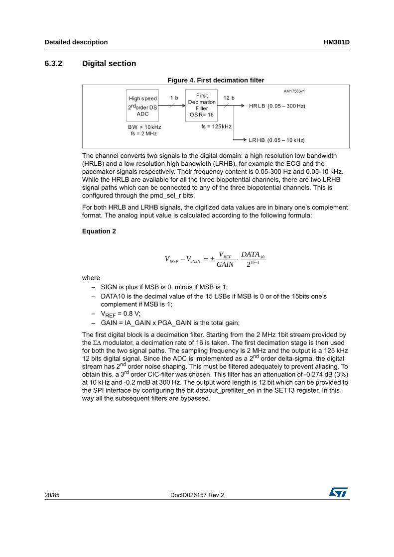
Figure 4. First decimation filter
The channel converts two signals to the digital domain: a high resolution low bandwidth (HRLB) and a low resolution high bandwidth (LRHB), for example the ECG and the pacemaker signals respectively. Their frequency content is 0.05-300 Hz and 0.05-10 kHz. While the HRLB are available for all the three biopotential channels, there are two LRHB signal paths which can be connected to any of the three biopotential channels. This is configured through the pmd_sel_r bits.
For both HRLB and LRHB signals, the digitized data values are in binary one’s complement format. The analog input value is calculated according to the following formula:
Equation 2
where
– SIGN is plus if MSB is 0, minus if MSB is 1;
– DATA10 is the decimal value of the 15 LSBs if MSB is 0 or of the 15bits one’s complement if MSB is 1;
– VREF = 0.8 V;
– GAIN = IA_GAIN x PGA_GAIN is the total gain;
The first digital block is a decimation filter. Starting from the 2 MHz 1bit stream provided by the modulator, a decimation rate of 16 is taken. The first decimation stage is then used for both the two signal paths. The sampling frequency is 2 MHz and the output is a 125 kHz 12 bits digital signal. Since the ADC is implemented as a 2nd order delta-sigma, the digital stream has 2nd order noise shaping. This must be filtered adequately to prevent aliasing. To obtain this, a 3rd order CIC-filter was chosen. This filter has an attenuation of -0.274 dB (3%) at 10 kHz and -0.2 mdB at 300 Hz. The output word length is 12 bit which can be provided to the SPI interface by configuring the bit dataout_prefilter_en in the SET13 register. In this way all the subsequent filters are bypassed.
AM17583v1
High speed
2rdorder DSADC
Firs tDecimation
F ilterOS R = 16
1 b 12 b
BW > 10 kHzfs = 2 MHz
fs = 125 kHz
HR LB (0.05 – 300 Hz)
LR HB (0.05 – 10 kHz)
11610
2 DATA
GAIN
VVV REF
INxNINxP

DocID026157 Rev 2 21/85
HM301D Detailed description
85
6.3.3 High resolution low bandwidth signal path (HRLB)
Figure 5. HRLB digital signal path
After the first decimation filter, a second decimation is performed in order to reduce the sampling frequency and, in the same time, to cut the high frequency signal part. The second decimation for HRLB signal is fixed to 32 and the output sampling frequency is 3.906 kHz. After that, a High Pass Filter is implemented. The -3 dB cut-off frequency is variable with 6 possible values: 0.05, 0.5, 0.7, 1, 2 and 5 Hz (hc_dig_ecghpf_sel_r<0:2>). After the HPF, a FIR filter with selectable bandwidth of 25, 37, 50, 75, 100, 150, 200 and 300 Hz (hc_dig_ecglpf_sel_r < 0 : 2 >) is implemented. At the end, a further decimation by 2 is inserted. Finally, the output signal is sent to the SPI block.
The following parameters can be set through the SPI interface:
Low Pass Filter cut-off frequency: 25, 37.5, 50, 75, 100, 150, 200, 300, 600 Hz (hc_dig_ecglpf_sel_r);
High Pass Filter cut-off frequency: 0.05, 0.5, 0.7, 1, 2, 5 Hz (hc_dig_ecghpf_sel_r);
Cut-off start frequency of the high pass digital filter for the start-up procedure (hc[1,2,3]_dig_hpf_sel_r). Active only when recovery mode is OFF.
6.3.4 Low resolution high bandwidth signal path (LRHB)
The LRHB signal path takes the same signal of 12 bits 125 kHz, coming from the 1st decimation filter, as input. Linear phase response is an important parameter. This can only be achieved by using FIR filters. Implementing FIR filters to filter a 5 kHz with a sampling frequency of 125 kHz will require a lot of taps in the filter. As with the HRLB path low pass filter, a decimation step is performed to lower the sampling frequency so to decrease the required taps in the FIR filters.
The LRHB signal can be provided with different cut off frequencies for low and high pass filters. As shown in Figure 6, the configuration of the digital blocks is changed in case of 5 kHz and 10 kHz low pass cut off frequencies.
A decimation step of 2 is done for the 10 kHz case and a decimation of 4 for the 5 kHz one, in this way the same FIR filter with only 4 taps is used in both cases. Implementing this decimation step with a good pass-band characteristic can be achieved with a CIC decimation filter.
For the 10 kHz low pass filter case, the FIR filter follows the first decimation filter, then a new decimation by 2 and finally the IIR high pass filter.
For the 5 kHz case, the FIR and IIR filters are swapped each other and, the decimation rate of the first filter is doubled.
AM17584v1
High P assFilter
0.05; 0.5; 0.7;1; 2; 5 Hz
FIR F ilterBW = 25; 37;50; 75; 100;
150; 200; 300
16 b 16 b DecimationOS R = 2
fs = 3.906 kHz fs = 0.163 –1.953 kHz
16 b
fs = 82 – 976 Hz
S P I16 bS econd
DecimationFilter
OS R = 32
fs = 3.906 kHz
HR LB (0.05 – 300 Hz)
12 b

Detailed description HM301D
22/85 DocID026157 Rev 2
Figure 6. LRHB signal path
The following parameters can be set through the SPI interface:
Low Pass Filter cut-off frequency: 5, 10 kHz (hc_dig_pmlpf_sel_r);
High Pass Filter cut-off frequency: 0.05, 0.7, 1, 5,1000 Hz (hc_dig_pmhpf_sel_r);
Connection of the two LRHB signal paths to any of the three biopotential channels (pm_sel_r);
The LRHB signal path provides also a signal amplitude detection function. This function is useful as pacemaker detection (PMD) in ECG systems where reduced ODR, fewer MIPS for the host and low power consumption are key features. Integrated hardware detection of the pacemaker pulse allows the device to meet these requirements.
The 9 most significant bits without sign of the LRHB (16 bit) are compared with a user selectable threshold of 9 bit (hc_pmd_thres_r). When the threshold value is higher than the absolute value of the LRHB signal the output signal (PMD) is asserted high. Two PMD signals are available at DGIO1 and DGIO2 outputs. In ECG application these signals provide the pace maker detection signal. Since the comparison is done at digital level, the threshold value must be changed according to the gain setting.
For example, if a 0.2 mV value must be detected at the input of the channel and the threshold is set at 000000001, since one LSB of the ADC is 24 µV, the 0.2 mV represents the 6th bit of the LRHB word with a gain of 8 or the 9th bit with a gain of 64. Since the comparison is done with the 9 MSBs, in the first case the PMD signal will be always low while in the second case the PMD will change in the same way as the 9th bit of the LRHB word.
6.4 Lead off detection
During ECG measurement and especially during a long period of monitoring, the electrode to skin contact check is needed in order to guarantee an adequate impedance value for a good signal acquisition. The HM301D provides two types of contact check: DC and AC
AM17585v1
DecimationF ilter
OS R = 2
F IR F ilterBW = 10 kHz
Decimationby
OS R = 2
16 b 16 b 16 b
fs = 62.5 kHz
IIR F ilterBW = 0.05 Hz;0.7 Hz; 1 Hz;5 Hz; 1 kHz
fs = 62.5 kHz fs = 31.25 kHz
16 b
fs = 31.25 kHz
S PI12 bDecF ilterby16
fs = 31.25 kHz
DecimationF ilter
OS R = 4
Decimationby
OS R = 2
16 b 16 b 16 b
fs = 31.25 kHzfs = 31.25 kHz fs = 15.625 kHz
16 b
fs = 15.625 kHz
S PI12 bDecF ilterby16
IIR F ilterBW = 0.05 Hz;0.7 Hz; 1 Hz;5 Hz; 1 kHz
fs = 15.625 kHz
F IR F ilterBW = 5 kHz
16 b12 b
(a) 10 KHz Low P ass F ilter
(a) 5 KHz Low Pass F ilter
DocID026157 Rev 2 23/85
HM301D Detailed description
85
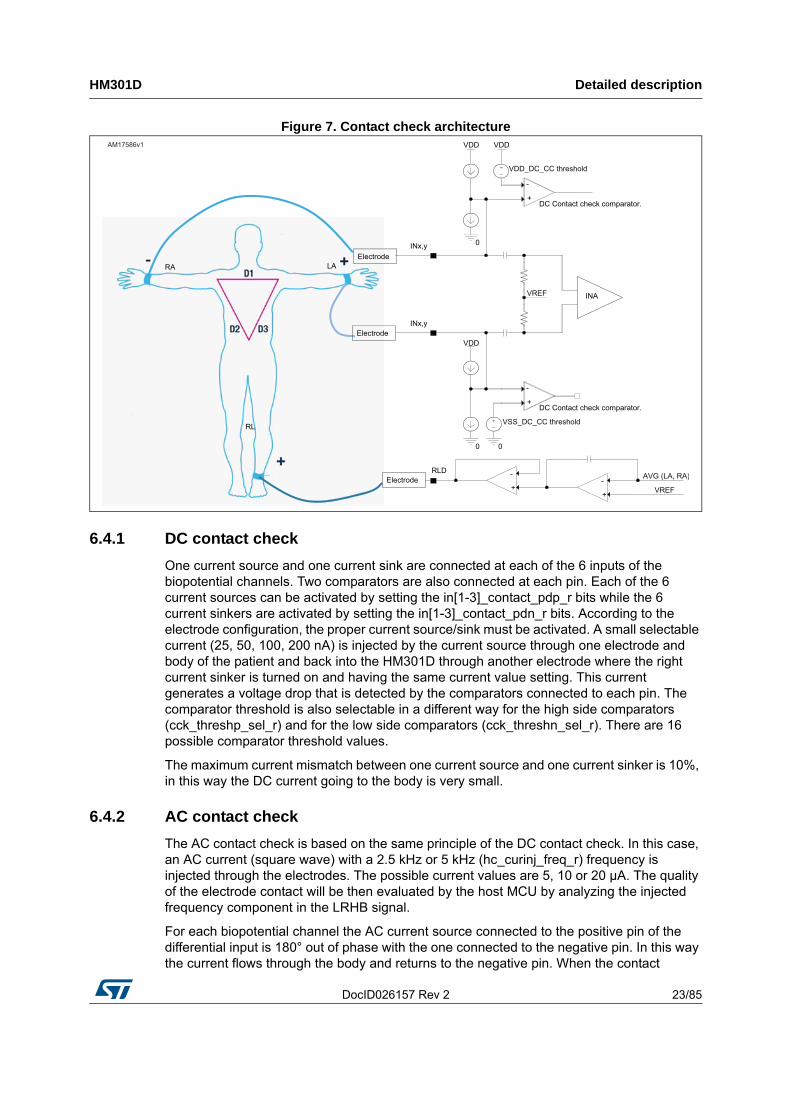
Figure 7. Contact check architecture
6.4.1 DC contact check
One current source and one current sink are connected at each of the 6 inputs of the biopotential channels. Two comparators are also connected at each pin. Each of the 6 current sources can be activated by setting the in[1-3]_contact_pdp_r bits while the 6 current sinkers are activated by setting the in[1-3]_contact_pdn_r bits. According to the electrode configuration, the proper current source/sink must be activated. A small selectable current (25, 50, 100, 200 nA) is injected by the current source through one electrode and body of the patient and back into the HM301D through another electrode where the right current sinker is turned on and having the same current value setting. This current generates a voltage drop that is detected by the comparators connected to each pin. The comparator threshold is also selectable in a different way for the high side comparators (cck_threshp_sel_r) and for the low side comparators (cck_threshn_sel_r). There are 16 possible comparator threshold values.
The maximum current mismatch between one current source and one current sinker is 10%, in this way the DC current going to the body is very small.
6.4.2 AC contact check
The AC contact check is based on the same principle of the DC contact check. In this case, an AC current (square wave) with a 2.5 kHz or 5 kHz (hc_curinj_freq_r) frequency is injected through the electrodes. The possible current values are 5, 10 or 20 µA. The quality of the electrode contact will be then evaluated by the host MCU by analyzing the injected frequency component in the LRHB signal.
For each biopotential channel the AC current source connected to the positive pin of the differential input is 180° out of phase with the one connected to the negative pin. In this way the current flows through the body and returns to the negative pin. When the contact
AM17586v1
VREF
VREF
AVG (LA, RA)
VDD_DC_CC threshold
+
-
+
-
+
-
VSS_DC_CC threshold
+
-
0
0
VDD
VDD
VDD
0
INA
INx,y
INx,y
ElectrodeRA LA
RL
RLD
DC Contact check comparator.
DC Contact check comparator.
Electrode
Electrode

Detailed description HM301D
24/85 DocID026157 Rev 2
between two electrodes, each connected to the positive or negative inputs of two different channels, has to be checked, then it is necessary to reverse the phase of one of two involved AC current generator. The hc[1-3]_phaserev_r bits allow doing it so that any electrode configuration can be implemented.
The AC current generator is enabled by setting the relative hc[1-3]_curinj_en_r bit. In addition, by setting the hc_curinj_en_ext bit it is possible to enable/disable the AC current generators through an external logic signal applied to the DIGIO2 pin. This signal will be AND-ed with the hc[1-3]_curinj_en_r bits, so that only the enabled current generators will be turned on.
6.5 Impedance channel
The goal of the impedance channel is to measure the impedance of the body and to measure the variation of this impedance due to the respiration. In reality the measured impedance won't be the impedance of the body alone but the series connection of the body with the board protections, the 2 electrodes and with skin and gel impedances. These values must be taken into account when reading the impedance values of HM301D.
The impedance circuit detects impedance values by injecting a high frequency square wave AC current through the CIP and CIN pins and monitoring the resulting voltage (Figure 8).
High frequency is imposed both for safety reasons and due to the electrodes' band pass. To avoid electrode polarization the average injected current is minimized.
Figure 8. Impedance channel architecture
The body impedance is used as an indicator to determine biological parameters, such as those used for galvanic skin response evaluation and patient fluid status check. Furthermore, in automated external defibrillator (AED) applications, body impedance evaluation is needed in order to deliver the proper amount of energy to the patient. This function has been designed considering application-specific electrodes (i.e. with polarity).
The modulated impedance (AC impedance) measurement principle is based on bio-impedance measurement on the patient's thorax and allows the measurement of respiration concurrently with the ECG and pacemaker measurements using two standard ECG electrodes. The time variation of body impedance due to respiration and chest movement is measured. This allows breath rate evaluation and provides information about movement artifacts that can affect ECG measurement.
AM17596v1
BPF20 – 50 kHz
LPF 1 Hz
DecimationFilter Demodulator
High speed3 ° order ΣΔ
ADC
Overflow
To digital
INA PGAHPF
ZDC_R
ZAC_R
LPF
From
Hea
lth C
hann
el 1
Gain =8,16GBW>2MHz
Gain =1,2,4GBW>2MHzfc<0.1kHz
Gain =1fc=250 kHz
LPF 1 – 20 HzHPF 0.05 Hz
LPF 1 Hz
LPF 1 – 20 HzHPF 0.05 Hz
ZDC_I
ZAC_I
Analog Digital
BW>10kHzfs =2 MHz
DocID026157 Rev 2 25/85
HM301D Detailed description
85
The impedance is measured by the injection of an AC current at 31.25 kHz and by measuring the resulting voltage across it. The current value can be chosen among three different values: 5, 10 and 20 µA. Since this current is injected using different pins from the ones where the voltage is measured, a 4 wire measure (force and sense principle) is implemented.
Even if unpractical in real applications, using 4 different electrodes is really helpful to improve the accuracy of the impedance measurement. Anyhow using only 2 electrodes but separating the PCB path of force and sense until the cable connector, will bypass all the impedances of the application (protections, PCB tracks, etc) which usually have higher values than the ones that must be measured. For example, in ECG systems, the defibrillator and ESD protection resistors could be as high as 25 k, while the measured body resistance is ~ 0.5 k.
The impedance channel differential input is connected to the same input of biopotential channel 1 (see Figure 1).
The impedance channel outputs a real part and an imaginary part of the modulated impedance. This is obtained by IQ demodulation in the digital part of the channel which introduces additional gain and phase shift.
6.5.1 Analog section
All analog blocks of the impedance channel are the same as their counterparts of the biopotential channel except for the low pass filter which has now a cut-off frequency of 250 kHz.
Another difference is the ADC which is now a 3th order cascaded (2-1) low pass-delta-sigma. A second order converter plus an extra stage that converts the quantization noise are implemented. Therefore the ADC will have 3th order noise shaping.
The following parameters can be set through the SPI interface:
Current injection frequency: 20, 25, 31, 35, 41, 45, 50 kHz (imp_curinj_freq_r);
Current injection value: 5, 10 20 µA (imp_curinj_cur_r);
IA Gain: 8, 16 (imp_ina_gain_r);
PGA Gain: 1,2, 4 (imp_pga_gain_r);
6.5.2 Digital section
Figure 9 shows the 3rd order ADC followed by the filters in the impedance channel. The signal is first decimated and band pass filtered so to get sampling frequency of 4 times the signal frequency. An IQ-demodulator splits the signal in a real (I) and imaginary (Q) component. The result is again decimated before a final high pass filter at 0.05 Hz and low pass filter at 20 Hz or 1 Hz. The high pass filter is used to extract the ac component in combination with the 20 Hz or (after extra decimation) 1 Hz low pass filter. For the dc-component, only the 1 Hz low pass filter is used, without the high pass filter.

Detailed description HM301D
26/85 DocID026157 Rev 2
Figure 9. Impedance channel digital section
The following parameters can be set through the SPI interface:
Digital Low Pass filter cut-off frequency: 1 or 20 Hz (imp_dif_lpf_sel_r)
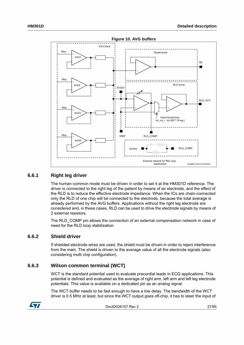
6.6 Drivers
The global architecture for the drivers is shown in Figure 10. The drivers operation is specifically designed for ECG systems. In particular the WCT (Wilson common terminal) is used in unipolar ECG systems, while RLD is the right leg driver for ECG which allows reducing system disturbances. The Shield driver is used in case of shielded cable.
An important role is played by the four AVG buffers. The positive inputs of these buffers are connected to any of the INxy pins by programming the input connection matrix (inputcon_avg[1-4]_r). In this way, the average value of any combination of the biopotential channels can be created. The output of the AVG buffers is fed to the shield driver and RLD driver. Each of the four AVG buffers can be turned on/off by setting the avg_en_buf[1-4]_r bit. It is important to turn on only the AVG buffers used because the summing resistors will be programmed according to the numbers of AVG buffers which are on.
In addition the right number of AVG buffers used must be written in the avg_numb_buf_r bits. This number will represent the total number of AVG buffers used also in the case of multiple connections of HM301D chips, where all the AVGIO pins are tied together.
The topology of the drivers is based on the following considerations:
It should not load the input signal. Therefore the electrode inputs are buffered with unity gain buffers.
The unipolar measurements should have similar accuracy as the bipolar measurements. This basically means that the total noise contribution of the 3 unity gain buffers must be smaller than the total noise contribution of the entire biopotential channel.
The bandwidth of the WCT circuit must be enough to not generate too much delay.
AM17612v1
AC component
ΣΔADCP os t-proc es s ing
F irs tDec imation
F ilterOS R = 25
5 b 16 b
fs = 2 MHz
B P Ffc = fs /4
IQDemodulation
16 b
Q16 b
I16 b 2°Dec imation
F ilterHP F
fc =0.05Hz
Dec imationand L P F
I
QDec imation
and L P FQ16 b
I16 b
fs = 4*fm
fm = modulation frequenc y
times temp = 1/fs
fs = 4*fm
DC component
I16 b
I16 b
Q16 b
Q16 b
DocID026157 Rev 2 27/85
HM301D Detailed description
85
Figure 10. AVG buffers
6.6.1 Right leg driver
The human common mode must be driven in order to set it at the HM301D reference. The driver is connected to the right leg of the patient by means of an electrode, and the effect of the RLD is to reduce the effective electrode impedance. When the ICs are chain-connected only the RLD of one chip will be connected to the electrode, because the total average is already performed by the AVG buffers. Applications without the right leg electrode are considered and, in these cases, RLD can be used to drive the electrode signals by means of 2 external resistors.
The RLD_COMP pin allows the connection of an external compensation network in case of need for the RLD loop stabilization.
6.6.2 Shield driver
If shielded electrode wires are used, the shield must be driven in order to reject interference from the main. The shield is driven to the average value of all the electrode signals (also considering multi chip configuration).
6.6.3 Wilson common terminal (WCT)
WCT is the standard potential used to evaluate precordial leads in ECG applications. This potential is defined and evaluated as the average of right arm, left arm and left leg electrode potentials. This value is available on a dedicated pin as an analog signal.
The WCT buffer needs to be fast enough to have a low delay. The bandwidth of the WCT driver is 0.5 MHz at least, but since the WCT output goes off-chip, it has to steer the input of
RLD_OUT
VREF
+
-
+
-
+
-
+
-
+
- -
+
INxy
INxy
INxy
INxy
AVG block
AVGIO RLD driver
-
+
Shield driver
SD
AVG1
AVG2
AVG3
AVG4
Open/closed looprld_cut_r bit (SET 19 reg.)
RLD_COMP
External network for RDL loop stabilization
RLD_COMPAVGIO
GAMS1103141035SG
Detailed description HM301D
28/85 DocID026157 Rev 2
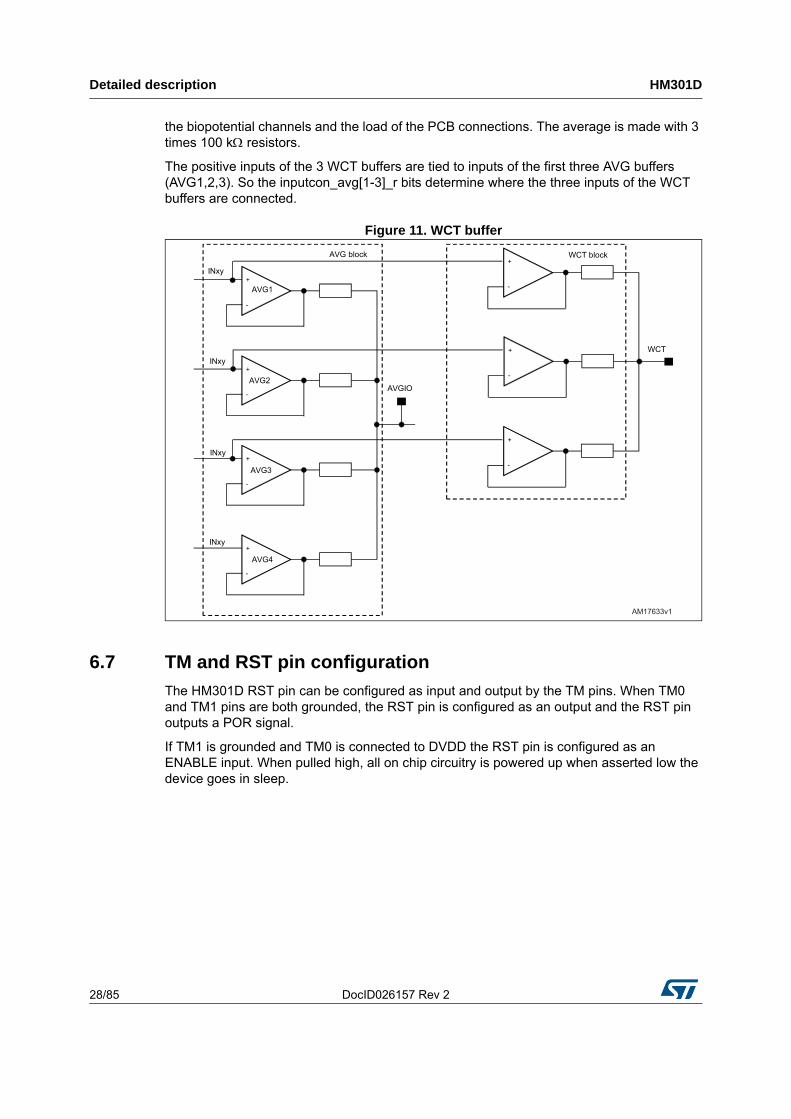
the biopotential channels and the load of the PCB connections. The average is made with 3 times 100 k resistors.
The positive inputs of the 3 WCT buffers are tied to inputs of the first three AVG buffers (AVG1,2,3). So the inputcon_avg[1-3]_r bits determine where the three inputs of the WCT buffers are connected.
Figure 11. WCT buffer
6.7 TM and RST pin configuration
The HM301D RST pin can be configured as input and output by the TM pins. When TM0 and TM1 pins are both grounded, the RST pin is configured as an output and the RST pin outputs a POR signal.
If TM1 is grounded and TM0 is connected to DVDD the RST pin is configured as an ENABLE input. When pulled high, all on chip circuitry is powered up when asserted low the device goes in sleep.
AM17633v1
+
-
+
-
+
-
+
-
INxy
INxy
INxy
INxy
AVG block
AVGIO
+
-
+
-
+
-AVG1
AVG2
AVG3
AVG4
WCT block
WCT

DocID026157 Rev 2 29/85
HM301D Detailed description
85
6.8 Digital machine
The digital part of the HM301D performs the preprocessing and filtering of all the digital signals coming from 4 analog channels. This part has been already described in the biopotential and impedance channel sections. In addition it manages all the device operation related to operating modes, trimming and test procedures, start-up sequence. The digital part can be configured through SPI and has a non-volatile memory which carries the trimming words for the analog building blocks. In HM301D the data can be retrieved by two methods: packets streaming mode and read data command mode. These two procedures can be selected by meas_mode bit (SET22 <7>).
6.8.1 Operating modes
The HM301D has the following operating states: sleep, boot, standby, ready, measure, recovery.
6.8.2 Sleep
This state is active when in any other state the RST pin is asserted low
6.8.3 Boot
This state is reached 100 µs after the RST pin is gone to VDD. This function is implemented with an internal counter so to wait the right time for the analog blocks to be stable. The device stays in this state for 600 µs before automatically moving to standby.
6.8.4 Standby
Packets streaming mode (meas_mode = 0).
This state is reachable in two ways:
– From Boot state. This means that the boot is correctly performed;
– From Measure state, by pulling up the CS pin. This means that the user asks to exit from the Measure mode in order to load through SPI a new configuration (see SPI communication for details).
Read data command mode (meas_mode = 1)
Table 10. Functional modes
TM1 TM0 RST pin Function Description
DVSS DVSS POR Digital Output
The RST pin outputs POR:
· High device off
· Low device on
DVSS DVDD EN Digital Input
The RST pin is configured as Enable:
· High power up
· Low power down
DVDD DVSS RES - Reserved
DVDD DVDD RES - Reserved

Detailed description HM301D
30/85 DocID026157 Rev 2
This state is reachable in two ways
– From Boot state. This means that the boot is correctly performed
– From Measure state putting the settings_ok_r bit to zero
6.8.5 Ready
This state is reached from Standby mode when the bit settings_ok_r (3Dh) is set to 1 and the clock is working correctly. This means that the user has loaded all the configurations and the clock is running correctly. This state is not present when meas_mode = 1.
6.8.6 Measure
Packets streaming mode (meas_mode = 0).
– This state is reachable from the in ready state putting the CS pin low. When entering the measure state the device automatically initiates a first fast recovery procedure end then outputs the data on SPI
– When in measure state the device can pass to stand-by state by pulling the CS pin high.
Read data command mode (meas_mode = 1)
– This state is reachable from standby state putting the settings_ok_r bit to 1. When entering the measure state the device automatically initiates a first fast recovery procedure.
– When in Measure state the device can pass to stand-by state setting the settings_ok_r bit to 1.
Figure 12. State machine for packets streaming mode (meas_mode = 0)
AM17613v1
Sleep
Measure
Ready
Boot
Standby
CS pin high

DocID026157 Rev 2 31/85
HM301D Detailed description
85
Figure 13. State machine for packets streaming mode (meas_mode = 1)
6.8.7 Fast recovery
During an overvoltage, overflow condition or at start-up, i.e. a condition where the input voltage is too large or zero, the digital state machine initiate the recovery mode.
This procedure is activated when entering the Measure state and when an overflow conditions lasts for a longer time than a programmed blanking time. This time is programmable from 2.5 ms to 37.5 ms in 2.5 ms steps by setting the recovery_time_r bits.
The recovery procedure can be disabled by setting recovery_time_r =1111. In this condition, the digital high pass filters are set by the hcx_dig_hpf_sel_r (registers 38h and 39h) and not by the hc_dig_ecghpf_sel_r and hc_dig_pmhpf_sel_r. With the recovery mode disabled, it is possible to change the cut off frequency of the analog high pass filters by changing the hc[1-3]_rhpf_sel_r bits.
At the beginning of the Recovery mode, the HP filters of all the channels, both in the digital as well as in the analog domain, are switched to their highest (5 Hz) cut-off frequency, then they are switched to lower frequencies. From 5 Hz the cut off is changed to 0.7 Hz and then to 0.05 Hz. The timing between two different cut-off frequencies is programmable between 0 and 1 s with 200 ms steps (filter_switchtime1_r / filter_switchtime2_r). So when the maximum time is chosen, the total recovery time is 2 s: 1s for the switching time from 5 Hz to 0.7 Hz and 1s for the switching time from 0.7 Hz to 0.05 Hz.
The digital HP filter is switched in the same way as the analog HP filter. The only difference is that it stops at the frequency which is selected by the hc_dig_ecghpf_sel_r and hc_dig_pmhpf_sel_r bits. For instance, if the user selects a HP cut-off of 0.7 Hz than the filter stops at 0.7 Hz. When it is 1 Hz the filter switches to 1 Hz instead of 0.7 Hz.
During recovery mode all the AC current injection blocks are disabled, so the signals, hcX_curinj_en and imp_curinj_en are set to 0.
AM17614v1
Sleep
Measure
Boot
Standby
settings_ok_r = 1
settings_ok_r = 0

Detailed description HM301D
32/85 DocID026157 Rev 2
6.9 GPIO configuration
The HM301D has 3 digital GPIOs. DGIO0 and DGIO1 are always used as outputs while DGIO2 can be configured as input or output by changing the dgio2_config_r bit (address 40h bit #2).
Each DGIO has his own multiplexer that can be configured by changing the corresponding digiox_mus_sel_r<3:0> (registers SET25 and SET26). The multiplexer configuration is shown in the following tables.
Table 11. Digital GPIO output signals (DGIO0)
Register SET 26 - address 46 hex - <7:4> DGIO0_muxsel_r <3:0>
DGIO0
0000 pm_rsh
0001 clk_o
0010 pmd1
0011 pmd2
0100 imp_adc_pdm1_o
0101 fchop_o
0110 por_o
0111 not used
1000 ecg_rsh
1001 z_rsh
1010 prefilt_rsh
1011 in_contact_out_flag1
1100 in_contact_out_flag4
1101 in_cck_out1
1110 in_cck_out4
1111 hc1_overfow_flag

DocID026157 Rev 2 33/85
HM301D Detailed description
85
Table 12. Digital GPIO output signals (DGIO1)
Register SET 25 - address 45 hex - <3:0> DGIO1_muxsel_r <3:0>
DGIO1
0000 pmd1
0001 hc1_adc_pdm_o
0010 hc2_adc_pdm_o
0011 hc3_adc_pdm_o
0100 imp_adc_pdm2_o
0101 psmon0
0110 not used
0111 ecg_rsh
1000 z_rsh
1001 prefilt_rsh
1010 pm_rsh
1011 in_contact_out_flag2
1100 in_contact_out_flag5
1101 in_cck_out2
1110 in_cck_out5
1111 hc2_overfow_flag

Detailed description HM301D
34/85 DocID026157 Rev 2
Description of the signals:
pm_rsh:
– This signal provides the information about a new data refresh of the LRHB signal path inside the HM301D. This signal must be used to synchronize the MCU readings. In this case the data must be retrieved using the data packet streaming procedure (Meas_mode=0). As soon this signal goes high, the MCU can send a train of 80 clock pulses in order to read 64 bits of the data stream.
ecg_rsh:
– This signal provides the information about a new data refresh of the HRLB signal path inside the HM301D. This signal must be used to synchronize the MCU readings. In this case the data must be retrieved using the normal SPI data reading procedure. As soon this signal goes high, the MCU must read directly the ECG_OUT registers using the word reading procedure as described in Figure 15. To enable the SPI data reading the Meas_mode bit in SET 22 register must be set to 1.
z_rsh:
– This signal provides the information about a new data refresh of the impedance channel path inside the HM301D. This signal must be used as trigger to synchronize the MCU readings. In this case the data must be retrieved using the normal SPI data reading procedure. As soon this signal goes high, the MCU must read directly the Impedance registers using the word reading procedure as described in Figure 15. To enable the SPI data reading the Meas_mode bit in SET 22 register must be set to 1
Table 13. Digital GPIO output signals (DGIO2)
Register SET 25 - address 45 hex - <7:4> DGIO2_muxsel_r <3:0>
DGIO2
(dgio2_config_r=1)
0000 pmd2
0001 hc1_overflow_o
0010 hc2_overflow_o
0011 hc3_overflow_o
0100 imp_overflow_o
0101 psmon1
0110 not used
0111 z_rsh
1000 pm_rsh
1001 imp_overfow_flag
1010 ecg_rsh
1011 in_contact_out_flag3
1100 in_contact_out_flag6
1101 in_cck_out3
1110 in_cck_out6
1111 hc3_overfow_flag

DocID026157 Rev 2 35/85
HM301D Detailed description
85
prefilt_rsh:
– This signal provides the information about a new data refresh of the pre-filtered signals. This signal must be used to synchronize the MCU readings. In this case the data must be retrieved using the data packet streaming procedure. As soon this signal goes high, the MCU can send a train of 48 clock pulses in order to read 64 bits of the pre-filtered data stream.
pmd1, pmd2:
– These signals represent the output of the signal amplitude detection of the LRHB signal path of the biopotential channels. pmd1 and pmd2 can be configured to provide the data of CH1, CH2 and CH3 according to the pm_sel_r bits (address 28h<6:4>).
hc1_adc_pdm_o, hc2_adc_pdm_o, hc3_adc_pdm_o:
– 1bit 2Mhz output streams of the ADCs of the three acquisition channels;
hc1_overflow_o, hc1_overflow_o, hc1_overflow_o, imp_overflow_o:
– Overflow signals of the three acquisition channels and impedance channel;
in_contact_out_flag1, in_contact_out_flag2, in_contact_out_flag3, in_contact_out_flag4, in_contact_out_flag5, in_contact_out_flag6: contact check flags go high if the comparator threshold is crossed. The status of this flags is latched out at the rising edge of internal generated clock.
in_contact_out1, in_contact_out2, in_contact_out3, in_contact_out4, in_contact_out5, in_contact_out6: outputs of the contact check comparator. These signals are the outputs of the contact check comparator and give the same information of the in_contact_out_flagx but in asynchronous way.
hc1_overfow_flag, hc1_overfow_flag, hc1_overfow_flag, imp_overfow_flag:
– HRLB channels and impedance channel overflow flags
imp_adc_pdm1_o:
– First bit of the stream of the ADC of the impedance channel;
imp_adc_pdm2_o:
– Second bit of the stream of the ADC of the impedance channel;
fchop_o:
– Chopping signal for the input amplifiers and signal for AC contact check current injection;
clk_o:
– oscillator output;
Por_o
– Power on reset signal.
psmon0, psmon1
– power supply voltage monitor (see Figure 6.11).
The DGIOx can be also configured as an input.
– To configure DGIO0 as input set dgio0_config_r bit=0 (SET23 DIGIO_IO address 40h bit #0).
– To configure DGIO1 as input set dgio1_config_r bit=0 (SET23 DIGIO_IO address 40h bit #1).
– To configure DGIO2 as input set dgio2_config_r bit=0 (SET23 DIGIO_IO address 40h bit #2).
Following two tables give an overview of the digital input and output mux configuration
Detailed description HM301D
36/85 DocID026157 Rev 2
impinj_ondem_en_i: when low, it disables impedance current injection;
accc_ondem_en_i: when low, it disables AC contact check current injection
By connecting these pins to an MCU IO it is possible to turn on/off the ac current injection and impedance without interrupting the data stream of the SPI port.
6.10 SPI interface
The HM301D SPI port works as a bus slave. The SPI allows writing and reading the registers of the device.
The Serial Interface works with 4 wires: CS, SPC, SDI and SDO.
When in measurement mode the SPI port works in a particular way where no address is needed for reading the data but the device automatically send out the data in a particular output format, see Section 6.13 for details.
The HM301D SPI is capable of being connected in a daisy chain when multiple chips are connected together (see Section 6.10.3).
CS is the serial port enable and it is controlled by the SPI master. It goes low at the start of the transmission and goes back high at the end. SPC is the serial port clock and it is controlled by the SPI master. It is stopped when CS is high (no transmission). SDI and SDO are respectively the serial port data input and output. Those lines are driven at the falling edge of SPC and should be captured at the rising edge of SPC. All the pins are idle when high.
6.10.1 SPI read
The read operation is performed by 32 clock pulses. In the first 16 pulses the master sends the read command byte and a dummy byte (FFh) through SDI pin with CS pin low. After that, the muster must put the CS pin high and send the second 16 clock pulses in order to output the read command byte and the data byte through the SDO pin. The read command byte contains the READ/WRITE bit (MSB) and the register address.
Table 14. Digital GPIO input signals
digioX_mux_sel[3:0] DIGIO0 DIGIO1 DIGIO2
0000 impinj_ondem_en_i accc_ondem_en_i

DocID026157 Rev 2 37/85
HM301D Detailed description
85
Figure 14. Single byte reading
The Figure 15 shows the procedure for a double byte reading.
Figure 15. Double byte reading
6.10.2 SPI write
The SPI Write command is performed with 16 clock pulses. In the first 8th bit the master sends the READ/WRITE command byte; in the second 8th bit the master sends the data byte to write. The command byte contains the READ/WRITE bit (MSB) and the register address (AD(6:0)). Both command byte and data byte must be written in MSB-first format.
Table 15. Read command bytes
WRITE bit (MSB) Register address
1 AD6 AD5 AD4 AD3 AD2 AD1 AD0

Detailed description HM301D
38/85 DocID026157 Rev 2
Figure 16. Single byte writing
6.10.3 Daisy chain SPI
In the daisy chain SPI configuration, the first slave input (SDI) is connected to the MOSI and the first slave output (SDO) is connected to the second slave input (SDI) and so on. The last slave output is connected to the MISO of the master.
Figure 17. Example of daisy chain SPI connection with 3 HM301D
During the period in which CS stays high, the SPI port of each slave is designed to send out during the second group of clock pulses an exact copy of what it received during the first group of clock pulses. So all the SPI ports work as shift registers. When CS is low, all the slaves execute the commands at their respective SDI inputs.
Table 16. Write command byte
WRITE bit (MSB) Register address
0 AD6 AD5 AD4 AD3 AD2 AD1 AD0
SPC
SDI HM301D
SDO Slave1
CS
SPC
SDI HM301D
SDO Slave2
CS
SPC
SDI HM301D
SDO Slave3
CS
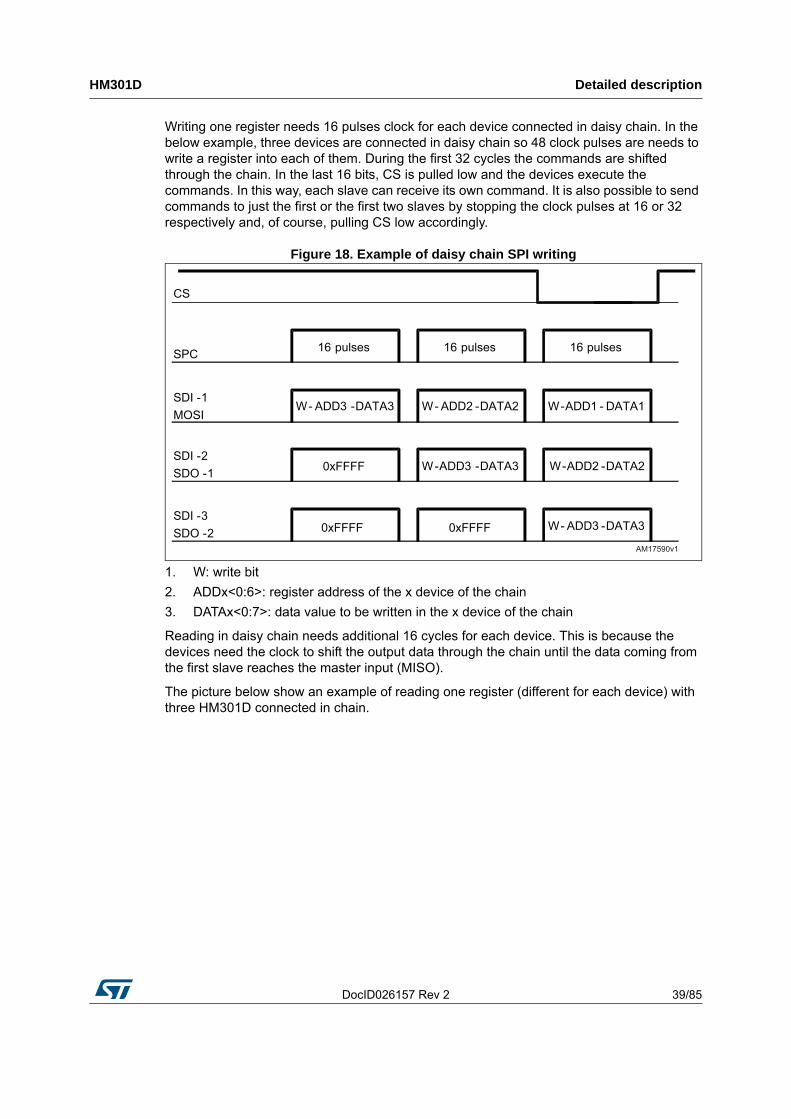
DocID026157 Rev 2 39/85
HM301D Detailed description
85
Writing one register needs 16 pulses clock for each device connected in daisy chain. In the below example, three devices are connected in daisy chain so 48 clock pulses are needs to write a register into each of them. During the first 32 cycles the commands are shifted through the chain. In the last 16 bits, CS is pulled low and the devices execute the commands. In this way, each slave can receive its own command. It is also possible to send commands to just the first or the first two slaves by stopping the clock pulses at 16 or 32 respectively and, of course, pulling CS low accordingly.
Figure 18. Example of daisy chain SPI writing
1. W: write bit
2. ADDx<0:6>: register address of the x device of the chain
3. DATAx<0:7>: data value to be written in the x device of the chain
Reading in daisy chain needs additional 16 cycles for each device. This is because the devices need the clock to shift the output data through the chain until the data coming from the first slave reaches the master input (MISO).
The picture below show an example of reading one register (different for each device) with three HM301D connected in chain.
AM17590v1
16 pulses 16 pulses 16 pulses
W- ADD3 -DATA3
0xFFFF
0xFFFF0xFFFF
CS
SPC
SDI -1MOSI
SDI -2 SDO -1
SDI -3SDO -2
W- ADD2 -DATA2 W-ADD1 - DATA1
W-ADD3 -DATA3 W-ADD2 -DATA2
W- ADD3 -DATA3

Detailed description HM301D
40/85 DocID026157 Rev 2
Figure 19. Example of daisy chain SPI reading
1. R: read bit
2. ADDx<0:6>: register address of the x device of the chain
3. DATAx<0:7>: data value read in the x device of the chain
See 0 for details about reading daisy chain SPI when HM301D is in measurement mode.
AM17591v1
16 pulses 16 pulses 16 pulses
R-ADD3 - 0xFF
0xFFFF
0xFFFF0xFFFF
CS
SPC
SDI-1MOSI
SDI -2 SDO-1
SDI-3SDO-2
R-ADD2 - 0xFF R-ADD1 - 0xFF
R-ADD3 - 0xFF R- ADD2 - 0xFF
R-ADD3 - 0xFF
0xFFFF0xFFFFSDO-3MISO
16 pulses 16 pulses 16 pulses
0xFFFF
0xFFFF 0xFFFF 0xFFFF
x - ADD1 - DATA1
x - ADD1 - DATA1
x - ADD1 - DATA1x - ADD2 - DATA2x - ADD3 - DATA3
x-ADD2 - DATA2
0xFFFF 0xFFFF
0xFFFF

DocID026157 Rev 2 41/85
HM301D Detailed description
85
6.10.4 SPI timing
Figure 20. SPI timing
4. Values are guaranteed at 10 MHz clock frequency for SPI with 4 wires, based on characterization results, not tested in production.
5. Measurement points are done at 0.2 IOVDD and 0.8 IOVDD, for both input and output port.
Table 17. SPI slave timings (IOVDD = 1.8 V)
Symbol Parameter Test condition Min. Max. Unit
tc (SPC) SPI clock cycle 100 ns
fc (SPC) SPI clock frequency 10 MHz
tsu (CS) CS setup time 6 ns
th (CS) CS hold time 8
tsu (SI) SDI input setup time 5
th (SI) SDI input hold time 15
tv (SO) SDO valid output time 50
th (SO) SDO output hold time 9
tdis (SO) SDO output disable time 50
AM17592v1
SPC
CS
SDI
SDO
tsu(CS)
tv(SO)tv(SO) th(SO)
th(SI)tsu(SI)
th(CS)
tdis(SO)
tc(SPC)
MSB IN
MSB OUT LSB OUT
LSB IN

Detailed description HM301D
42/85 DocID026157 Rev 2
6.11 Power supply voltage monitor
The HM301D is able to monitor the level of analog supply voltage and to give a 2 bits signal named psmon_out. The table below shows the meaning of the psmon_out<1:0>.
The psmon_out signal is available for SPI reading in the OUT_FLAG1 register (48h) or in the DIGIO1 and DGIO2 with proper configuration of DGIO multiplexer.
6.12 Registers MAP
Table 18. Psmon_out signal
psmon_out_i<1:0> Supply level
00 AVDD < 1.62 V
01 1.62 V < AVDD < 2.13 V
10 2.13 V < AVDD < 3.6 V
11 AVDD > 3.6 V
Table 19. Registers MAP
Register name Register description Sub address Type
SET0 Enable bits 27h R/W
SET1 Active Pacemaker channels, current injection enables
28h R/W
SET2 AVG Buffers 29h R/W
SET3 Multi chip configuration, input matrix configuration
2Ah R/W
SET4 input matrix configuration 2Bh R/W
SET5 input matrix configuration 2Ch R/W
SET6 input matrix configuration 2Dh R/W
SET7 input matrix configuration 2Eh R/W
SET8 Clock configuration, RLD connection 2Fh R/W
SET9 DC contact check settings 30h R/W
SET10 DC contact check settings 31h R/W
SET11 DC contact check settings 32h R/W
SET12 DC contact check comparators settings 33h R/W
SET13 Gain of biopotential channels, AC contact check current injection
34h R/W
SET14 Impedance channel settings 35h R/W
SET15 Gain of impedance channel, LPF and HPF settings of LBHR path
36h R/W

DocID026157 Rev 2 43/85
HM301D Detailed description
85
SET16 LPF and HPF settings of HBLR path 37h R/W
SET17 Fast startup settings of analog and digital HP filter
38h R/W
SET18 39h R/W
SET19 AC current injection phase, RLD settings, LPF of impedance channel
3Ah R/W
SET20 Recovery time settings, PM detection threshold
3Bh R/W
SET21 PM detection threshold 3Ch R/W
SET22 Start output data, HP filter switching time at start-up
3Dh R/W
SET23 DIGIO2 input or output configuration 40h R/W
SET24 Enable psmon, chop, current injection 44h R/W
SET25 Multiplexer configuration for Digital GPIOs DIGIO1 and DIGIO2
45h R/W
SET26 Multiplexer configuration for Digital GPIO DIGIO0
46h R/W
Output Flags (READ ONLY)
OUT_FLAG0 Overflow flags 47h R
OUT_FLAG1 DC contact check flags 48h R
Table 19. Registers MAP (continued)
Register name Register description Sub address Type

Detailed description HM301D
44/85 DocID026157 Rev 2
Table 20. Registers MAP
Register name Register description Sub address Type
ECG1_DATAOUT_1 49h R
ECG1_DATAOUT_0 4Ah R
ECG2_DATAOUT_1 4Bh R
ECG2_DATAOUT_0 4Ch R
ECG3_DATAOUT_1 4Dh R
ECG3_DATAOUT_0 4Eh R
ECG12_DATAOUT_1 4Fh R
ECG12_DATAOUT_0 50h R
ECG23_DATAOUT_1 51h R
ECG23_DATAOUT_0 52h R
ECG31_DATAOUT_1 53h R
ECG31_DATAOUT_0 54h R
PM1_DATAOUT_1 55h R
PM1_DATAOUT_0 56h R
PM2_DATAOUT_1 57h R
PM2_DATAOUT_0 58h R
IMPEDANCE_PHASE_AC_DATAOUT_1 59h R
IMPEDANCE_PHASE_AC_DATAOUT_0 5Ah R
IMPEDANCE_SQUARING_AC_DATAOUT_1 5Bh R
IMPEDANCE_SQUARING_AC_DATAOUT_0 5Ch R
IMPEDANCE_PHASE_DC_DATAOUT_1 5Dh R
IMPEDANCE_PHASE_DC_DATAOUT_0 5Eh R
IMPEDANCE_SQUARING_DC_DATAOUT_1 5Fh R
IMPEDANCE_SQUARING_DC_DATAOUT_0 60h R
CONTACT_CHECK_ DATAOUT_1 61h R
CONTACT_CHECK_ DATAOUT_0 62h R
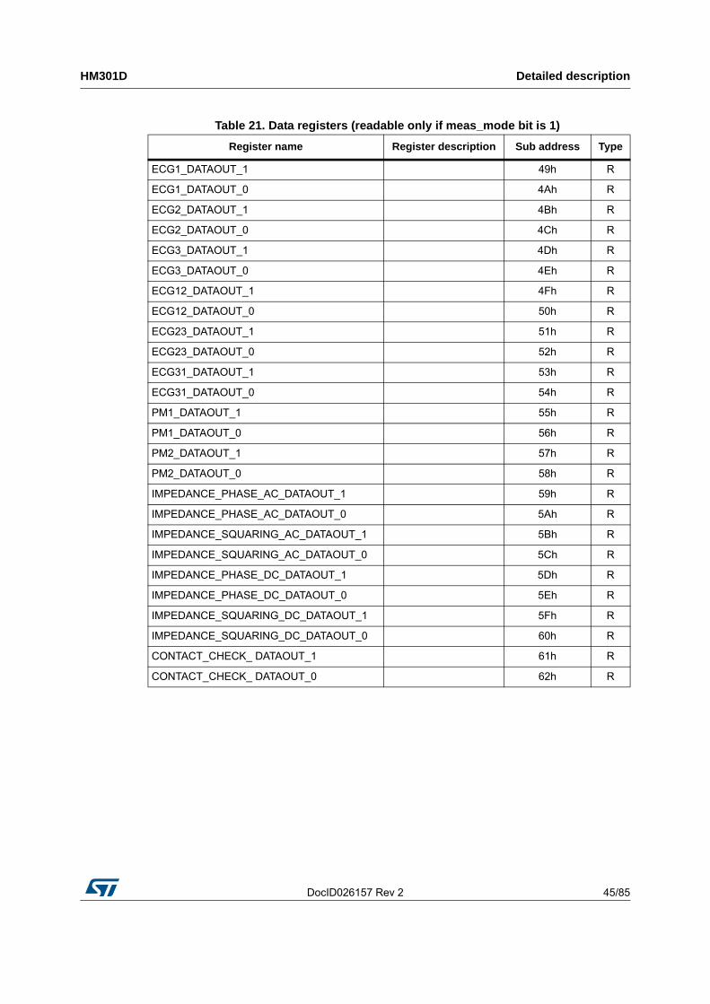
DocID026157 Rev 2 45/85
HM301D Detailed description
85
Table 21. Data registers (readable only if meas_mode bit is 1)
Register name Register description Sub address Type
ECG1_DATAOUT_1 49h R
ECG1_DATAOUT_0 4Ah R
ECG2_DATAOUT_1 4Bh R
ECG2_DATAOUT_0 4Ch R
ECG3_DATAOUT_1 4Dh R
ECG3_DATAOUT_0 4Eh R
ECG12_DATAOUT_1 4Fh R
ECG12_DATAOUT_0 50h R
ECG23_DATAOUT_1 51h R
ECG23_DATAOUT_0 52h R
ECG31_DATAOUT_1 53h R
ECG31_DATAOUT_0 54h R
PM1_DATAOUT_1 55h R
PM1_DATAOUT_0 56h R
PM2_DATAOUT_1 57h R
PM2_DATAOUT_0 58h R
IMPEDANCE_PHASE_AC_DATAOUT_1 59h R
IMPEDANCE_PHASE_AC_DATAOUT_0 5Ah R
IMPEDANCE_SQUARING_AC_DATAOUT_1 5Bh R
IMPEDANCE_SQUARING_AC_DATAOUT_0 5Ch R
IMPEDANCE_PHASE_DC_DATAOUT_1 5Dh R
IMPEDANCE_PHASE_DC_DATAOUT_0 5Eh R
IMPEDANCE_SQUARING_DC_DATAOUT_1 5Fh R
IMPEDANCE_SQUARING_DC_DATAOUT_0 60h R
CONTACT_CHECK_ DATAOUT_1 61h R
CONTACT_CHECK_ DATAOUT_0 62h R

Detailed description HM301D
46/85 DocID026157 Rev 2
6.12.1 Application settings (Read/Write)
Table 22. SET0 CH_ENABLE (ADDR 27h)
BIT Name Default Description
7 sd_en_r 0 Enable Shield driver
6 wct_en_r 0 Enable ALL WCT buffers
5 dig_en_r 0 Enable digital filtering of ALL health channels
4 d2se_en_r 0 Enable diff2se buffer of ALL health channels
3 imp_en_r 0 Enable Impedance Channel
2 hc3_en_r 0 Enable Health Channel 3
1 hc2_en_r 0 Enable Health Channel 2
0 hc1_en_r 0 Enable Health Channel 1
Table 23. SET1 PM_SEL (ADDR 28h)
BIT Name Default Description Configurations
7 DUMMY 0
6pm_sel_r<2>
0
Select active LRHB channels:
000 --> LRHB1 data from CH1; LRHB2 OFF
5pm_sel_r<1>
0 001 --> LRHB1 data from CH2; LRHB2 OFF
4pm_sel_r<0>
0 010 --> LRHB1 data from CH3; LRHB2 OFF
011 --> LRHB1 data from CH1; LRHB2 data from CH2
100 --> LRHB1 data from CH1; LRHB2 data from CH3
101 --> LRHB1 data from CH2; LRHB2 data from CH3
110 --> LRHB1 OFF; LRHB2 OFF
111 --> LRHB1 OFF; LRHB2 OFF
3 hc3_curinj_en_r 0 Enable health channel 3 current injection
2 hc2_curinj_en_r 0 Enable health channel 2 current injection
1 hc1_curinj_en_r 0 Enable health channel 1 current injection
0 rld_en_r 0 Enable RLD driver

DocID026157 Rev 2 47/85
HM301D Detailed description
85
Table 24. SET 2 AVG_CTRL (ADDR 29h)
BIT Name Default Description Configurations
7 avg_numb_buf_r<3> 0
Number of AVG buffers used in the system, this determines the compensation capacitance
0000 --> 0
6 avg_numb_buf_r<2> 0 0001 --> 1
5 avg_numb_buf_r<1> 0 0010 --> 2
4 avg_numb_buf_r<0> 0 0011 --> 3
………
1111 --> 15
3 avg_en_buf4_r 0 Enable AVG buffer 4
2 avg_en_buf3_r 0 Enable AVG buffer 3
1 avg_en_buf2_r 0 Enable AVG buffer 2
0 avg_en_buf1_r 0 Enable AVG buffer 1
Table 25. SET3 INCON_HCSEL_1 (2Ah)
BIT Name Default Description Configurations
7 ndev_bit1 0
Number of devices in application:
00 --> 1 device
6 ndev_bit0 0 01 --> 2 devices
10 --> 3 devices
11 --> 4 devices
5 inputcon_in1n_hcsel_r<2> 1
Connect input pad IN1N to one of the 6 health channel inputs
000 --> CH1 positive
4 inputcon_in1n_hcsel_r<1> 1 001 --> CH1 negative
3 inputcon_in1n_hcsel_r<0> 1 010 --> CH2 positive
011 --> CH2 negative
100 --> CH3 positive
101 --> CH3 negative
110 --> unconnected
111 --> unconnected
2 inputcon_in1p_hcsel_r<2> 1Connect input pad IN1P to one of the 6 channel inputs
Same setting of inputcon_in1n_hcsel_r
1 inputcon_in1p_hcsel_r<1> 1
0 inputcon_in1p_hcsel_r<0> 1
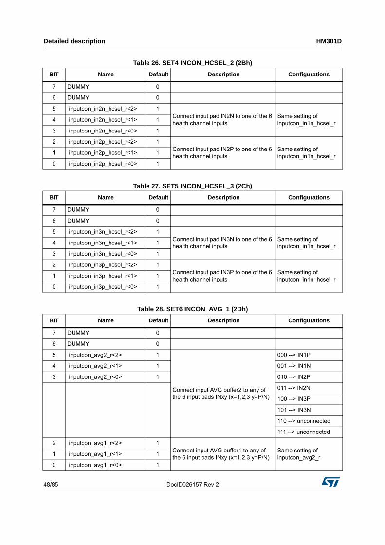
Detailed description HM301D
48/85 DocID026157 Rev 2
Table 26. SET4 INCON_HCSEL_2 (2Bh)
BIT Name Default Description Configurations
7 DUMMY 0
6 DUMMY 0
5 inputcon_in2n_hcsel_r<2> 1Connect input pad IN2N to one of the 6 health channel inputs
Same setting of inputcon_in1n_hcsel_r
4 inputcon_in2n_hcsel_r<1> 1
3 inputcon_in2n_hcsel_r<0> 1
2 inputcon_in2p_hcsel_r<2> 1Connect input pad IN2P to one of the 6 health channel inputs
Same setting of inputcon_in1n_hcsel_r
1 inputcon_in2p_hcsel_r<1> 1
0 inputcon_in2p_hcsel_r<0> 1
Table 27. SET5 INCON_HCSEL_3 (2Ch)
BIT Name Default Description Configurations
7 DUMMY 0
6 DUMMY 0
5 inputcon_in3n_hcsel_r<2> 1Connect input pad IN3N to one of the 6 health channel inputs
Same setting of inputcon_in1n_hcsel_r
4 inputcon_in3n_hcsel_r<1> 1
3 inputcon_in3n_hcsel_r<0> 1
2 inputcon_in3p_hcsel_r<2> 1Connect input pad IN3P to one of the 6 health channel inputs
Same setting of inputcon_in1n_hcsel_r
1 inputcon_in3p_hcsel_r<1> 1
0 inputcon_in3p_hcsel_r<0> 1
Table 28. SET6 INCON_AVG_1 (2Dh)
BIT Name Default Description Configurations
7 DUMMY 0
6 DUMMY 0
5 inputcon_avg2_r<2> 1
Connect input AVG buffer2 to any of the 6 input pads INxy (x=1,2,3 y=P/N)
000 --> IN1P
4 inputcon_avg2_r<1> 1 001 --> IN1N
3 inputcon_avg2_r<0> 1 010 --> IN2P
011 --> IN2N
100 --> IN3P
101 --> IN3N
110 --> unconnected
111 --> unconnected
2 inputcon_avg1_r<2> 1Connect input AVG buffer1 to any of the 6 input pads INxy (x=1,2,3 y=P/N)
Same setting of inputcon_avg2_r
1 inputcon_avg1_r<1> 1
0 inputcon_avg1_r<0> 1

DocID026157 Rev 2 49/85
HM301D Detailed description
85
Table 29. SET7 INCON_AVG_2 (2Eh)
BIT Name Default Description Configurations
7 DUMMY 0
6 DUMMY 0
5 inputcon_avg4_r<2> 1Connect input AVG buffer4 to any of the 6 input pads INxy (x=1,2,3 y=P/N)
Same setting of inputcon_avg2_r
4 inputcon_avg4_r<1> 1
3 inputcon_avg4_r<0> 1
2 inputcon_avg3_r<2> 1Connect input AVG buffer3 to any of the 6 input pads INxy (x=1,2,3 y=P/N)
Same setting of inputcon_avg2_r
1 inputcon_avg3_r<1> 1
0 inputcon_avg3_r<0> 1
Table 30. SET8 INCON_RLD (2Fh)
BIT Name Default Description Configurations
7 DUMMY 0
6 ckext_en 0 Enable clock output0: no clock out on ckext pin 1: clock out on ckext pin
5 clk_sel_r<1> 0Select the internal, external or XTAL oscillator
00 --> Ring Oscillator
4 clk_sel_r<0> 0 01 --> Xtal Oscillator
10 --> External clock
3 psmon_sel_r 1
Change the Common mode voltage of INA.
0-> VREF=0.7V
To use when supply voltage is lower than 2V, typical 1.8V
1-> VREF=1,0V
To use when supply voltage is higher than 2V, typical 3.3V.
2 inputcon_rld_sel_r<2> 1
Connect the RLD output to any of the inputs pads INxN/P, for x=1,2,3
000 --> IN1P
1 inputcon_rld_sel_r<1> 1 001 --> IN1N
0 inputcon_rld_sel_r<0> 1 010 --> IN2P
011 --> IN2N
100 --> IN3P
101 --> IN3N
110 --> unconnected
111 --> unconnected

Detailed description HM301D
50/85 DocID026157 Rev 2
Table 31. SET9 CCK_EN_1 (30h)
BIT Name Default Description Configurations
7 In2n_contact_pdn_r 0Contact check enable signal for N-side of DC contact check connected to in IN2N
0: current off
1: current on
6 In2n_contact_pdp_r 0Contact check enable signal for P-side of DC contact check connected to IN2N
Same as IN2N_contact_en_r
5 In2p_contact_pdn_r 0Contact check enable signal for N-side of DC contact check connected to IN2P
4 In2p_contact_pdp_r 0Contact check enable signal for P-side of DC contact check connected to IN2P
3 In1n_contact_pdn_r 0Contact check enable signal for N-side of DC contact check connected to IN1N
2 In1n_contact_pdp_r 0Contact check enable signal for P-side of DC contact check connected to IN1N
1 in1p_contact_pdn_r 0Contact check enable signal for N-side of DC contact check connected to IN1P
0 in1p_contact_pdp_r 0Contact check enable signal for P-side of DC contact check connected to IN1P
Table 32. SET10 CCK_EN_2 (31h)
BIT Name Default Description Configurations
7 in1n_cont_cur_r<1> 0
Select the current (25/50/100/200nA) of the contact check connected to IN1N
00 --> 25 nA
6 in1n_cont_cur_r<0> 0 01 --> 50 nA
10 --> 100 nA
11 --> 200 nA
5 in1p_cont_cur_r<1> 0 Select the current (25/50/100/200nA) of the contact check connected to IN1P
Same setting of in1n_cont_cur_r4 in1p_cont_cur_r<0> 0
3 in3n_contact_pdn_r 0Contact check enable signal for N-side of DC contact check connected to IN3N
2 in3n_contact_pdp_r 0Contact check enable signal for P-side of DC contact check connected to IN3N
1 in3p_contact_pdn_r 0Contact check enable signal for N-side of DC contact check connected to IN3P
0 in3p_contact_pdp_r 0Contact check enable signal for P-side of DC contact check connected to IN3P

DocID026157 Rev 2 51/85
HM301D Detailed description
85
Table 33. SET11 CCK_CUR (32h)
BIT Name Default Description Configurations
7 in3n_cont_cur_r<1> 0 Select the current (25/50/100/200nA) of the contact check connected to IN3N
Same setting of in1n_cont_cur_r6 in3n_cont_cur_r<0> 0
5 in3p_cont_cur_r<1> 0 Select the current (25/50/100/200nA) of the contact check connected to IN3P
Same setting of in1n_cont_cur_r4 in3p_cont_cur_r<0> 0
3 in2n_cont_cur_r<1> 0 Select the current (25/50/100/200nA) of the contact check connected to IN2N
Same setting of in1n_cont_cur_r2 in2n_cont_cur_r<0> 0
1 in2p_cont_cur_r<1> 0 Select the current (25/50/100/200nA) of the contact check connected to IN2P
Same setting of in1n_cont_cur_r0 in2p_cont_cur_r<0> 0

Detailed description HM301D
52/85 DocID026157 Rev 2
Table 34. SET12 CCK_TRSH (33h)
BIT Name Default Description Configurations
7 cck_threshp_sel_r<3> 0
Select threshold at the Vdd side for the DC contact at ALL inputs (typical values)
0000 --> VDD-60uV
6 cck_threshp_sel_r<2> 0 0001 --> VDD-102mV
5 cck_threshp_sel_r<1> 0 0010 --> VDD-204 mV
4 cck_threshp_sel_r<0> 0 0011 --> VDD-306mV
0100 --> VDD-408 mV
0101 --> VDD-510mV
0110 --> VDD-612mV
0111 --> VDD-714mV
1000 --> VDD-816mV
1001 --> VDD-918mV
1010 --> VDD-1.020 V
1011 --> VDD- 1.122 V
1100 --> VDD-1.224 V
1101 --> VDD-1.326 V
1110 --> VDD-1.427 V
1111 --> VDD-1.529 V
3 cck_threshn_sel_r<3> 0
Select threshold at the VSS side for the DC contact at ALL inputs (typical values)
0000 --> 60uV
2 cck_threshn_sel_r<2> 0 0001 --> 102mV
1 cck_threshn_sel_r<1> 0 0010 --> 204 mV
0 cck_threshn_sel_r<0> 0 0011 --> 306mV
0100 --> 408 mV
0101 --> 510mV
0110 --> 612mV
0111 --> 714mV
1000 --> 816mV
1001 --> 918mV
1010 --> 1.020 V
1011 --> 1.122 V
1100 --> 1.224 V
1101 --> 1.326 V
1110 --> 1. 427 V

DocID026157 Rev 2 53/85
HM301D Detailed description
85
Table 35. SET13 HC_ANA_CTRL (34h)
BIT Name Default Description Configurations
7 dataout_prefilter_en 0 Enable for data out pre-filter
6 hc_pga_gain_r<1> 1
Select the gain of the PGA (1, 2, 4) for ALL health channels
00 --> 4
5 hc_pga_gain_r<0> 1 01 --> 2
10 --> 4/3
11 --> 1
4 hc_ina_gain_r<1> 0
Select the gain of the INA (8 or 16) for ALL health channels
00 --> 8
3 hc_ina_gain_r<0> 0 01 --> 8
10 --> 16
11 --> 16
2 hc_curinj_freq_r 0 Select the current injection frequency (2,5kHz or 5kHz) for ALL health channels
0 --> 2.5 kHz
1 --> 5 kHz
1 hc_curinj_cur_r<1> 0Select the current injection (5uA, 10uA or 20uA) ALL health channels
00 --> 5 µA
0 hc_curinj_cur_r<0> 0 01 --> 10 µA
10 --> 20 µA
Table 36. SET14 IMP_ANA_CTRL (35h)
BIT Name Default Description Configurations
7 DUMMY 0
6 imp_ina_gain_r<1> 0
Select the gain of the INA (8 or 16) for the impedance channel
00 --> 8
5 imp_ina_gain_r<0> 0 01 --> 8
10 --> 16
11 --> 16
4 imp_curinj_cur_r<1> 0Select the current injection (5 µA, 10 µA or 20 µA) impedance channel
00 --> 5 µA
3 imp_curinj_cur_r<0> 0 01 --> 10 µA
10 --> 20 µA
2 imp_curinj_freq_r<2> 0
Select the current injection frequency. This is equal to the chopping frequency
000 --> fchop = 20 kHz
1 imp_curinj_freq_r<1> 0 001 --> fchop = 25 kHz
0 imp_curinj_freq_r<0> 0 010 --> fchop = 31.25 kHz
011 --> fchop = 35.714 kHz
100 --> fchop = 41.667 kHz
101 --> fchop = 45.455 kHz
110 --> fchop = 50 kHz

Detailed description HM301D
54/85 DocID026157 Rev 2
Table 37. SET15 ECG_DIGFILT_CTRL (36h)
BIT Name Default Description Configurations
7 hc_dig_ecghpf_sel_r<2> 1
Digital HPF cut-off frequency selection for the HRLB signal of ALL health channels.
These settings are active when the Recovery mode is ON.
000 --> 5 Hz
6 hc_dig_ecghpf_sel_r<1> 1 001 --> 2 Hz
5 hc_dig_ecghpf_sel_r<0> 0 010 --> 1 Hz
011 --> 0.7 Hz
100 --> 0.5 Hz
101 --> 0.1 Hz
110--> 0.05 Hz
4 hc_dig_ecglpf_sel_r<3> 0
Digital LPF cut-off frequency selection for the HRLB signal of ALL health channels.
1000 --> 600 Hz
3 hc_dig_ecglpf_sel_r<2> 0 0000 --> 300 Hz
2 hc_dig_ecglpf_sel_r<1> 0 0001 --> 200 Hz
1 hc_dig_ecglpf_sel_r<0> 0 0010 --> 150 Hz
0011 --> 100 Hz
0100 --> 75 Hz
0101 --> 50 Hz
0110 --> 37.5 Hz
0111 --> 25 Hz
0 DUMMY 0
Table 38. SET16 PM_DIGFILT_CTRL (37h)
BIT Name Default Description Configurations
7 DUMMY 0
6 imp_pga_gain_r<1> 0Select the gain of the PGA (1, 2, 4) for the impedance channel
00 --> 4
01 --> 2
5 imp_pga_gain_r<0> 010 --> 4/3
11 --> 1
4 DUMMY 0
3 hc_dig_pmhpf_sel_r<2> 0Digital HPF cut-off frequency selection for the LRHB signal of ALL health channels.
These settings are active when the Recovery mode is ON.
000 --> 5 Hz
2 hc_dig_pmhpf_sel_r<1> 1 001 --> 1 Hz
1 hc_dig_pmhpf_sel_r<0> 1 010 --> 0.7 Hz
011 --> 0.05 Hz
100 --> 1 kHz
0 hc_dig_pmlpf_sel_r 0 Digital LPF cut-off frequency selection for the LRHB signal of ALL health channels.
0 --> 10 kHz
1 --> 5 kHz

DocID026157 Rev 2 55/85
HM301D Detailed description
85
Table 39. SET17 HC_DIGFILT_CTRL (38h)
BIT Name Default Description Configurations
7 hc3_dig_hpf_sel_r<2> 0
Digital HP cut off frequency for health channel 3.
These settings are active when the Recovery mode is OFF
000 --> HRLB = 5Hz; LRHB = 5Hz
6 hc3_dig_hpf_sel_r<1> 0 001 --> HRLB = 2Hz; LRHB = 1Hz
5 hc3_dig_hpf_sel_r<0> 0 010 --> HRLB = 1Hz; LRHB = 1Hz
011 --> HRLB = 0.7Hz; LRHB = 0.7Hz
100 --> HRLB = 0.5Hz; LRHB = 0.7Hz
101 --> HRLB = 0.1Hz; LRHB = 0.05Hz
110 --> HRLB = 0.05Hz; LRHB = 0.05Hz
4 hc2_dig_hpf_sel_r<2> 0 Digital HP cut off frequency for health channel 2.
These settings are active when the Recovery mode is OFF
Same setting of hc3_dig_hpf_sel_r3 hc2_dig_hpf_sel_r<1> 0
2 hc2_dig_hpf_sel_r<0> 0
1 hc1_dig_hpf_sel_r<2> 0 Digital HP cut off frequency for health channel 1.
These settings are active when the Recovery mode is OFF
Same setting of hc3_dig_hpf_sel_r0 hc1_dig_hpf_sel_r<1> 0
Table 40. SET18 HC_HPFANA_CTRL (39h)
BIT Name Default Description Configurations
7 hc1_dig_hpf_sel_r<0> 0
6 DUMMY 0
5 hc3_rhpf_sel_r<1> 0 Select cut-off frequency of analog filter connected to HC3.
These settings are active when the Recovery mode is OFF. When Recovery mode is ON they are set at 0.05Hz.
00 --> 5Hz
4 hc3_rhpf_sel_r<0> 0 01 --> 0.7Hz
10 --> 0.05Hz
11 --> 0.05Hz
3 hc2_rhpf_sel_r<1> 0 Select cut-off frequency of analog filter connected to HC2.
These settings are active when the Recovery mode is OFF. When Recovery mode is ON they are set at 0.05Hz.
Same setting of hc3_rhpf_sel_r2 hc2_rhpf_sel_r<0> 0
1 hc1_rhpf_sel_r<1> 0 Select cut-off frequency of analog filter connected to HC1.
These settings are active when the Recovery mode is OFF. When Recovery mode is ON they are set at 0.05Hz.
Same setting of hc3_rhpf_sel_r0 hc1_rhpf_sel_r<0> 0

Detailed description HM301D
56/85 DocID026157 Rev 2
Table 41. SET19 RLD_CTRL (3Ah)
BIT Name Default Description Configurations
7 hc3_phaserev_r 0Reverse the phase of the injection frequency of health channel 3. Used in unipolar measurements.
6 hc2_phaserev_r 0Reverse the phase of the injection frequency of health channel 2. Used in unipolar measurements.
5 hc1_phaserev_r 0Reverse the phase of the injection frequency of health channel 1. Used in unipolar measurements.
4 rld_ref_sel_r<1> 0
Select reference for RLD
00 --> 0.7 V
3 rld_ref_sel_r<0> 0 01 --> 1 V
10 --> 1.49 V
2 vref_sel_r 0Register to select internal or external reference. 0->external reference;1-> internal reference
1 rld_cut_r 0Register to cut or close RLD loop
0 --> Closed
1 --> Open
0 imp_dig_lpf_sel_r 0 Digital LPF cut-off frequency selection for impedance channel
0 --> 20 Hz
1 --> 1 Hz

DocID026157 Rev 2 57/85
HM301D Detailed description
85
Table 42. SET20 RECOVERY_TIME (3Bh)
BIT Name Default Description Configurations
7 DUMMY 0
6 DUMMY 0
5 DUMMY 0
4 recovery_time_r<3> 0
Select the blanking time for overflow detection in steps of 2,5 ms. From 2,5 till 37,5ms. Can be put OFF as well.
0000 --> 2.5 ms
3 recovery_time_r<2> 0 0001 --> 5 ms
2 recovery_time_r<1> 0 0010 --> 7.5 ms
1 recovery_time_r<0> 0 0011 --> 10 ms
0100 --> 12.5 ms
0101 --> 15 ms
0110 --> 17.5 ms
0111 --> 20 ms
1000 --> 22.5 ms
1001 --> 25 ms
1010 --> 27.5 ms
1011 --> 30 ms
1100 --> 32.5 ms
1101 --> 35 ms
1110 --> 37.5 ms
1111 --> Recovery Mode OFF
0 hc_pmd_thres_r<8> 0 Pacemaker detection threshold
Table 43. SET21 PMD_TRSH (3Ch)
BIT Name Default Description Configurations
7 hc_pmd_thres_r<7> 0
Pacemaker detection threshold
6 hc_pmd_thres_r<6> 0
5 hc_pmd_thres_r<5> 0
4 hc_pmd_thres_r<4> 0
3 hc_pmd_thres_r<3> 0
2 hc_pmd_thres_r<2> 0
1 hc_pmd_thres_r<1> 0
0 hc_pmd_thres_r<0> 0

Detailed description HM301D
58/85 DocID026157 Rev 2
Table 44. SET22 FILTER_SWTIME (3Dh)
BIT Name Default Description Configurations
7 Meas_mode 0 Measurement mode selection0-> packets streaming
1-> read data command
6 settings_ok_r 0 Starts measurement mode
5 filter_switchtime2_r<2> 0
Select the switching time for the 2nd cut-off frequency step 0,7Hz-0,05Hz
000 --> 200 ms
4 filter_switchtime2_r<1> 0 001 --> 400 ms
3 filter_switchtime2_r<0> 0 010 --> 600 ms
011 --> 800 ms
100 to 111 --> 1 s
2 filter_switchtime1_r<2> 0Select the switching time for the first cut-off frequency step 5Hz-0,7Hz
Same setting of filter_switchtime2_r
1 filter_switchtime1_r<1> 0
0 filter_switchtime1_r<0> 0
Table 45. SET23 DIGIO_IO (40h)
BIT Name Default Description
7 DUMMY 0
6 DUMMY 0
5 DUMMY 0
4 DUMMY 0
3 DUMMY 0
2 digio2_config_r 1To configure DIGIOx in input or output mode
0: input; 1: output1 digio1_config_r 1
0 digio0_config_r 1
Table 46. SET24 IMP_CUR_EN (44h)
BIT Name Default Description
7 DUMMY 0
6 imp_curinj_en_r 1 Enable impedance current injection (CIP, CIN current generators)
5 Reserved 0
4 Reserved 0
3 Reserved 0
2 Reserved 0
1 Reserved 0
0 Reserved 0

DocID026157 Rev 2 59/85
HM301D Detailed description
85
Table 47. SET25 DIGIO12_SEL (45h)
BIT Name Default Description
7 Digio2_muxsel_r<3> 0
Select input signal for DIGIO26 Digio2_muxsel_r<2> 0
5 Digio2_muxsel_r<1> 0
4 Digio2_muxsel_r<0> 0
3 Digio1_muxsel_r<3> 0
Select input signal for DIGIO12 Digio1_muxsel_r<2> 0
1 Digio1_muxsel_r<1> 0
0 Digio1_muxsel_r<0> 0
Table 48. SET26 DIGIO0_SEL (46h)
BIT Name Default Description
7 Digio0_muxsel_r<3> 0
Select input signal for DIGIO06 Digio0_muxsel_r<2> 0
5 Digio0_muxsel_r<1> 0
4 Digio0_muxsel_r<0> 0
3 DUMMY 0
2 DUMMY 0
1 DUMMY 0
0 DUMMY 0

Detailed description HM301D
60/85 DocID026157 Rev 2
6.12.2 Output flags (read only)
Table 49. OUT_FLAG0 (47h)
BIT Name Def. Description
7 DUMMY
6 imp_overflow_r 0 Impedance Channel is in overflow mode
5 hc3_overflow_r 0 Channel 3 is in overflow mode
4 hc2_overflow_r 0 Channel 2 is in overflow mode
3 hc1_overflow_r 0 Channel 1 is in overflow mode
2 DUMMY 0
1 DUMMY 0
0 DUMMY 0
Table 50. OUT_FLAG1 (48h)
BIT Name Def. Description
7 psmon_out_r<1> 0
6 psmon_out_r<0> 0
5 In3n_contact_out_r 0 IN3N has bad contact. This is an OR of in3n_contact_outp_i &
in3n_contact_outn_i
4 In3p_contact_out_r 0 IN3P has bad contact. This is an OR of in3p_contact_outp_i &
in3p_contact_outn_i
3 In2n_contact_out_r 0 IN2N has bad contact. This is an OR of in2n_contact_outp_i &
in2n_contact_outn_i
2 In2p_contact_out_r 0 IN2P has bad contact. This is an OR of in2p_contact_outp_i &
in2p_contact_outn_i
1 in1n_contact_out_r 0 IN1N has bad contact. This is an OR of in1n_contact_outp_i &
in1n_contact_outn_i
0 in1_contact_out_r 0 IN1P has bad contact. This is an OR of in1p_contact_outp_i &
in1p_contact_outn_i
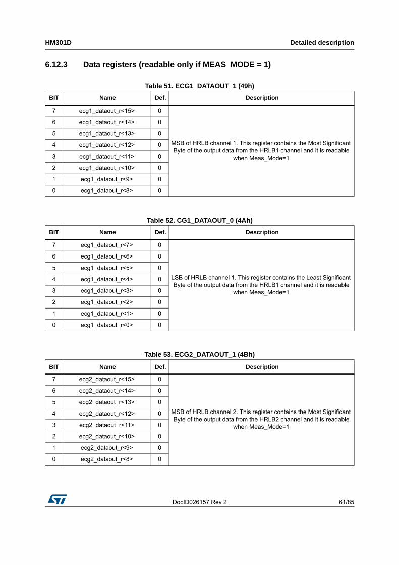
DocID026157 Rev 2 61/85
HM301D Detailed description
85
6.12.3 Data registers (readable only if MEAS_MODE = 1)
Table 51. ECG1_DATAOUT_1 (49h)
BIT Name Def. Description
7 ecg1_dataout_r<15> 0
MSB of HRLB channel 1. This register contains the Most Significant Byte of the output data from the HRLB1 channel and it is readable
when Meas_Mode=1
6 ecg1_dataout_r<14> 0
5 ecg1_dataout_r<13> 0
4 ecg1_dataout_r<12> 0
3 ecg1_dataout_r<11> 0
2 ecg1_dataout_r<10> 0
1 ecg1_dataout_r<9> 0
0 ecg1_dataout_r<8> 0
Table 52. CG1_DATAOUT_0 (4Ah)
BIT Name Def. Description
7 ecg1_dataout_r<7> 0
LSB of HRLB channel 1. This register contains the Least Significant Byte of the output data from the HRLB1 channel and it is readable
when Meas_Mode=1
6 ecg1_dataout_r<6> 0
5 ecg1_dataout_r<5> 0
4 ecg1_dataout_r<4> 0
3 ecg1_dataout_r<3> 0
2 ecg1_dataout_r<2> 0
1 ecg1_dataout_r<1> 0
0 ecg1_dataout_r<0> 0
Table 53. ECG2_DATAOUT_1 (4Bh)
BIT Name Def. Description
7 ecg2_dataout_r<15> 0
MSB of HRLB channel 2. This register contains the Most Significant Byte of the output data from the HRLB2 channel and it is readable
when Meas_Mode=1
6 ecg2_dataout_r<14> 0
5 ecg2_dataout_r<13> 0
4 ecg2_dataout_r<12> 0
3 ecg2_dataout_r<11> 0
2 ecg2_dataout_r<10> 0
1 ecg2_dataout_r<9> 0
0 ecg2_dataout_r<8> 0
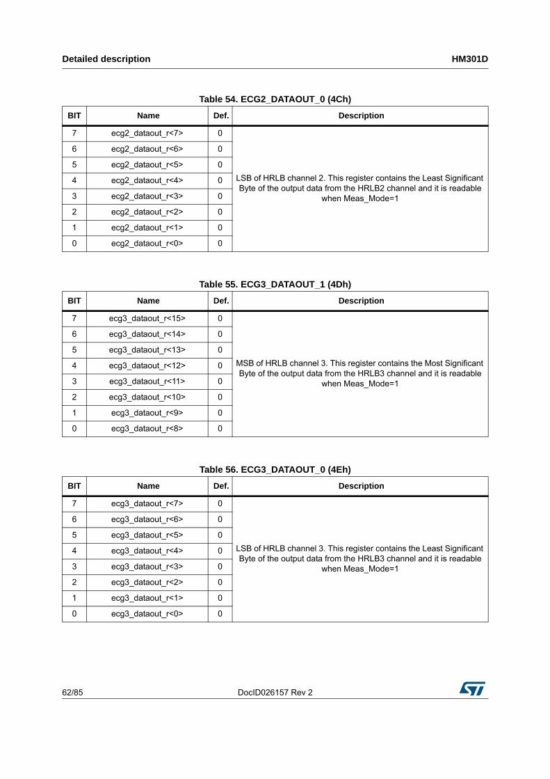
Detailed description HM301D
62/85 DocID026157 Rev 2
Table 54. ECG2_DATAOUT_0 (4Ch)
BIT Name Def. Description
7 ecg2_dataout_r<7> 0
LSB of HRLB channel 2. This register contains the Least Significant Byte of the output data from the HRLB2 channel and it is readable
when Meas_Mode=1
6 ecg2_dataout_r<6> 0
5 ecg2_dataout_r<5> 0
4 ecg2_dataout_r<4> 0
3 ecg2_dataout_r<3> 0
2 ecg2_dataout_r<2> 0
1 ecg2_dataout_r<1> 0
0 ecg2_dataout_r<0> 0
Table 55. ECG3_DATAOUT_1 (4Dh)
BIT Name Def. Description
7 ecg3_dataout_r<15> 0
MSB of HRLB channel 3. This register contains the Most Significant Byte of the output data from the HRLB3 channel and it is readable
when Meas_Mode=1
6 ecg3_dataout_r<14> 0
5 ecg3_dataout_r<13> 0
4 ecg3_dataout_r<12> 0
3 ecg3_dataout_r<11> 0
2 ecg3_dataout_r<10> 0
1 ecg3_dataout_r<9> 0
0 ecg3_dataout_r<8> 0
Table 56. ECG3_DATAOUT_0 (4Eh)
BIT Name Def. Description
7 ecg3_dataout_r<7> 0
LSB of HRLB channel 3. This register contains the Least Significant Byte of the output data from the HRLB3 channel and it is readable
when Meas_Mode=1
6 ecg3_dataout_r<6> 0
5 ecg3_dataout_r<5> 0
4 ecg3_dataout_r<4> 0
3 ecg3_dataout_r<3> 0
2 ecg3_dataout_r<2> 0
1 ecg3_dataout_r<1> 0
0 ecg3_dataout_r<0> 0

DocID026157 Rev 2 63/85
HM301D Detailed description
85
Table 57. ECG12_DATAOUT_1 (4Fh)
BIT Name Def. Description
7 ecg3_dataout_r<15> 0
MSB of ECG12_dataout. This register contains the Most Significant Byte of the half sum between the output data from the ECG1 Chain and the output data from the ECG2 Chain and it is readable when
Meas_Mode=1
6 ecg3_dataout_r<14> 0
5 ecg3_dataout_r<13> 0
4 ecg3_dataout_r<12> 0
3 ecg3_dataout_r<11> 0
2 ecg3_dataout_r<10> 0
1 ecg3_dataout_r<9> 0
0 ecg3_dataout_r<8> 0
Table 58. ECG12_DATAOUT_0 (50h)
BIT Name Def. Description
7 ecg3_dataout_r<7> 0
LSB of ECG12_dataout. This register contains the Least Significant Byte of the half sum between the output data from the ECG1 Chain and the output data from the ECG2 Chain and it is readable when
Meas_Mode=1
6 ecg3_dataout_r<6> 0
5 ecg3_dataout_r<5> 0
4 ecg3_dataout_r<4> 0
3 ecg3_dataout_r<3> 0
2 ecg3_dataout_r<2> 0
1 ecg3_dataout_r<1> 0
0 ecg3_dataout_r<0> 0
Table 59. ECG23_DATAOUT_1 (51h)
BIT Name Def. Description
7 ecg3_dataout_r<15> 0
MSB of ECG23_dataout. This register contains the Most Significant Byte of the half sum between the output data from the ECG2 Chain and the output data from the ECG3 Chain and it is readable when
Meas_Mode=1
6 ecg3_dataout_r<14> 0
5 ecg3_dataout_r<13> 0
4 ecg3_dataout_r<12> 0
3 ecg3_dataout_r<11> 0
2 ecg3_dataout_r<10> 0
1 ecg3_dataout_r<9> 0
0 ecg3_dataout_r<8> 0
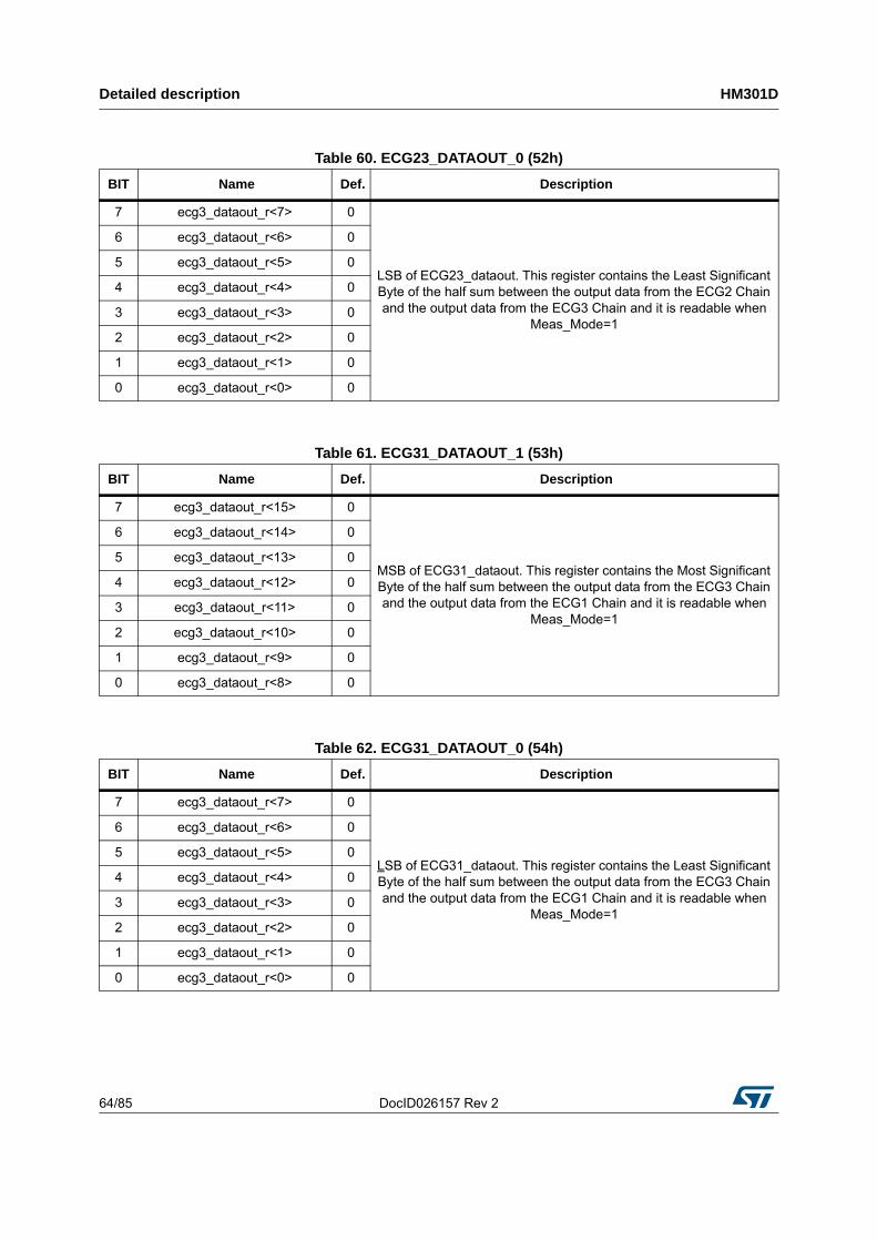
Detailed description HM301D
64/85 DocID026157 Rev 2
Table 60. ECG23_DATAOUT_0 (52h)
BIT Name Def. Description
7 ecg3_dataout_r<7> 0
LSB of ECG23_dataout. This register contains the Least Significant Byte of the half sum between the output data from the ECG2 Chain and the output data from the ECG3 Chain and it is readable when
Meas_Mode=1
6 ecg3_dataout_r<6> 0
5 ecg3_dataout_r<5> 0
4 ecg3_dataout_r<4> 0
3 ecg3_dataout_r<3> 0
2 ecg3_dataout_r<2> 0
1 ecg3_dataout_r<1> 0
0 ecg3_dataout_r<0> 0
Table 61. ECG31_DATAOUT_1 (53h)
BIT Name Def. Description
7 ecg3_dataout_r<15> 0
MSB of ECG31_dataout. This register contains the Most Significant Byte of the half sum between the output data from the ECG3 Chain and the output data from the ECG1 Chain and it is readable when
Meas_Mode=1
6 ecg3_dataout_r<14> 0
5 ecg3_dataout_r<13> 0
4 ecg3_dataout_r<12> 0
3 ecg3_dataout_r<11> 0
2 ecg3_dataout_r<10> 0
1 ecg3_dataout_r<9> 0
0 ecg3_dataout_r<8> 0
Table 62. ECG31_DATAOUT_0 (54h)
BIT Name Def. Description
7 ecg3_dataout_r<7> 0
LSB of ECG31_dataout. This register contains the Least Significant Byte of the half sum between the output data from the ECG3 Chain and the output data from the ECG1 Chain and it is readable when
Meas_Mode=1
6 ecg3_dataout_r<6> 0
5 ecg3_dataout_r<5> 0
4 ecg3_dataout_r<4> 0
3 ecg3_dataout_r<3> 0
2 ecg3_dataout_r<2> 0
1 ecg3_dataout_r<1> 0
0 ecg3_dataout_r<0> 0

DocID026157 Rev 2 65/85
HM301D Detailed description
85
Table 63. PM1_DATAOUT_1 (55h)
BIT Name Def. Description
7 pm1_dataout_r<15> 0
MSB of LRHB channel 1. This register contains the Most Significant Byte of the output data from the LRHB 1 channel and it is readable
when Meas_Mode=1
6 pm1_dataout_r<14> 0
5 pm1_dataout_r<13> 0
4 pm1_dataout_r<12> 0
3 pm1_dataout_r<11> 0
2 pm1_dataout_r<10> 0
1 pm1_dataout_r<9> 0
0 pm1_dataout_r<8> 0
Table 64. PM1_DATAOUT_0 (56h)
BIT Name Def. Description
7 pm1_dataout_r<7> 0
LSB of LRHB channel 1. This register contains the Least Significant Byte of the output data from the LRHB1 channel and it is readable
when Meas_Mode=1
6 pm1_dataout_r<6> 0
5 pm1_dataout_r<5> 0
4 pm1_dataout_r<4> 0
3 pm1_dataout_r<3> 0
2 pm1_dataout_r<2> 0
1 pm1_dataout_r<1> 0
0 pm1_dataout_r<0> 0
Table 65. PM2_DATAOUT_1 (57h)
BIT Name Def. Description
7 pm2_dataout_r<15> 0
MSB of LRHB channel 2. This register contains the Most Significant Byte of the output data from the LRHB2 channel and it is readable
when Meas_Mode=1
6 pm2_dataout_r<14> 0
5 pm2_dataout_r<13> 0
4 pm2_dataout_r<12> 0
3 pm2_dataout_r<11> 0
2 pm2_dataout_r<10> 0
1 pm2_dataout_r<9> 0
0 pm2_dataout_r<8> 0
Detailed description HM301D
66/85 DocID026157 Rev 2
Table 66. PM2_DATAOUT_0 (58h)
BIT Name Def. Description
7 pm2_dataout_r<7> 0
LSB of LRHB channel 2. This register contains the Least Significant Byte of the output data from the LRHB2 channel and it is readable
when Meas_Mode=1
6 pm2_dataout_r<6> 0
5 pm2_dataout_r<5> 0
4 pm2_dataout_r<4> 0
3 pm2_dataout_r<3> 0
2 pm2_dataout_r<2> 0
1 pm2_dataout_r<1> 0
0 pm2_dataout_r<0> 0
Table 67. IMPEDANCE_PHASE_AC_DATAOUT_1 (59h)
BIT Name Def. Description
7 impp_ac_dataout_r<15> 0
MSB of IMPP_AC_dataout. This register contains the Most Significant Byte of the output data from the IMPEDANCE PHASE
AC and it is readable when Meas_Mode=1
6 impp_ac_dataout_r<14> 0
5 impp_ac_dataout_r<13> 0
4 impp_ac_dataout_r<12> 0
3 impp_ac_dataout_r<11> 0
2 impp_ac_dataout_r<10> 0
1 impp_ac_dataout_r<9> 0
0 impp_ac_dataout_r<8> 0
Table 68. IMPEDANCE_PHASE_AC_DATAOUT_0 (5Ah)
BIT Name Def. Description
7 impp_ac_dataout_r<7> 0
LSB of IMPP_AC_dataout. This register contains the Least Significant Byte of the output data from the IMPEDANCE PHASE
AC and it is readable when Meas_Mode=1
6 impp_ac_dataout_r<6> 0
5 impp_ac_dataout_r<5> 0
4 impp_ac_dataout_r<4> 0
3 impp_ac_dataout_r<3> 0
2 impp_ac_dataout_r<2> 0
1 impp_ac_dataout_r<1> 0
0 impp_ac_dataout_r<0> 0
DocID026157 Rev 2 67/85
HM301D Detailed description
85
Table 69. IMPEDANCE_SQUARING_AC_DATAOUT_1 (5Bh)
BIT Name Def. Description
7 impq_ac_dataout_r<15> 0
MSB of IMPQ_AC_dataout. This register contains the Most Significant Byte of the output data from the IMPEDANCE SQUARING AC and it is readable when Meas_Mode=1
6 impq _ac_dataout_r<14> 0
5 impq _ac_dataout_r<13> 0
4 impq _ac_dataout_r<12> 0
3 impq _ac_dataout_r<11> 0
2 impq _ac_dataout_r<10> 0
1 impq _ac_dataout_r<9> 0
0 impq _ac_dataout_r<8> 0
Table 70. IMPEDANCE_SQUARING_AC_DATAOUT_0 (5Ch)
BIT Name Def. Description
7 impq _ac_dataout_r<7> 0
LSB of IMPP_AC_dataout. This register contains the Least Significant Byte of the output data from the IMPEDANCE SQUARING AC and it is readable when Meas_Mode=1
6 impq _ac_dataout_r<6> 0
5 impq _ac_dataout_r<5> 0
4 impq _ac_dataout_r<4> 0
3 impq _ac_dataout_r<3> 0
2 impq _ac_dataout_r<2> 0
1 impq _ac_dataout_r<1> 0
0 impq _ac_dataout_r<0> 0
Table 71. IMPEDANCE_PHASE_DC_DATAOUT_1 (5Dh)
BIT Name Def. Description
7 impp_dc_dataout_r<15> 0
MSB of IMPP_DC_dataout. This register contains the Most Significant Byte of the output data from the IMPEDANCE PHASE
DC and it is readable when Meas_Mode=1
6 impp_dc_dataout_r<14> 0
5 impp_dc_dataout_r<13> 0
4 impp_dc_dataout_r<12> 0
3 impp_dc_dataout_r<11> 0
2 impp_dc_dataout_r<10> 0
1 impp_dc_dataout_r<9> 0
0 impp_dc_dataout_r<8> 0

Detailed description HM301D
68/85 DocID026157 Rev 2
Table 72. IMPEDANCE_PHASE_DC_DATAOUT_0 (5Eh)
BIT Name Def. Description
7 impp_dc_dataout_r<7> 0
LSB of IMPP_DC_dataout. This register contains the Least Significant Byte of the output data from the IMPEDANCE PHASE
DC and it is readable when Meas_Mode=1
6 impp_dc_dataout_r<6> 0
5 impp_dc_dataout_r<5> 0
4 impp_dc_dataout_r<4> 0
3 impp_dc_dataout_r<3> 0
2 impp_dc_dataout_r<2> 0
1 impp_dc_dataout_r<1> 0
0 impp_dc_dataout_r<0> 0
Table 73. IMPEDANCE_SQUARING_DC_DATAOUT_1 (5Fh)
BIT Name Def. Description
7 impq_dc_dataout_r<15> 0
MSB of IMPQ_DC_dataout. This register contains the Most Significant Byte of the output data from the IMPEDANCE SQUARING DC and it is readable when Meas_Mode=1
6 impq _dc_dataout_r<14> 0
5 impq _dc_dataout_r<13> 0
4 impq _dc_dataout_r<12> 0
3 impq _dc_dataout_r<11> 0
2 impq _dc_dataout_r<10> 0
1 impq _dc_dataout_r<9> 0
0 impq _dc_dataout_r<8> 0
Table 74. IMPEDANCE_SQUARING_DC_DATAOUT_0 (60h)
BIT Name Def. Description
7 impq _dc_dataout_r<7> 0
LSB of IMPP_DC_dataout. This register contains the Least Significant Byte of the output data from the IMPEDANCE SQUARING DC and it is readable when Meas_Mode=1
6 impq _dc_dataout_r<6> 0
5 impq _dc_dataout_r<5> 0
4 impq _dc_dataout_r<4> 0
3 impq _dc_dataout_r<3> 0
2 impq _dc_dataout_r<2> 0
1 impq _dc_dataout_r<1> 0
0 impq _dc_dataout_r<0> 0
DocID026157 Rev 2 69/85
HM301D Detailed description
85
6.13 Output data format
In order to optimize the communication between the HM301D and the microcontroller, the HM301D implements an automatic data transmission able to minimize the communication load. In order to read the device data, the MCU doesn't need to send the register addresses to the device but it is the HM301D which continuously sends the data to the MCU. These data are organized in a packet which presents an added header in order to describe the meaning of the data included inside the packet. Anyhow the MCU can stop the data flow by pulling up the CS pin anytime.
All the data values are in binary twos complement format. The table below shows the ideal codes:
Table 75. CONTACT_CHECK_DATAOUT_1 (61h)
BIT Name Def. Description
7 dummy 0
MSB of CC_dataout. This register contains the Most Significant Byte of the output data from the CONTACT CHECK and it is readable
when Meas_Mode=1
6 dummy 0
5 overcurr_p 0
4 overcurr_n 0
3 psmon1 0
2 psmon0 0
1 imp_overflow_flags 0
0 hc_overflow_flag3 0
Table 76. CONTACT_CHECK_DATAOUT_0 (62h)
BIT Name Def. Description
7 hc_overflow_flag2 0
LSB of CC_dataout. This register contains the Least Significant Byte of the output data from the CONTACT CHECK and it is readable
when Meas_Mode=1
6 hc_overflow_flag1 0
5 in_contact_out_flag6 0
4 in_contact_out_flag5 0
3 in_contact_out_flag4 0
2 in_contact_out_flag3 0
1 in_contact_out_flag2 0
0 in_contact_out_flag1 0

Detailed description HM301D
70/85 DocID026157 Rev 2
The HM301D can send the processed data of biopotential channels and impedance channel or the raw data of the biopotential channels just after the first decimation filters (see Figure 4).
The data packet is different according to the type of data that is transmitted.
6.13.1 Case 1: complete processed data - 4x packet
In this case the packet will be formed by four words of 16 bits each (base packet). In case of multi-chip configuration each device provides its own base packet. Those base packets are organized in the following way.
where the c_data can be a biopotential data vector or an impedance data vector or a miscellaneous data vector. In multi-chip configuration, the packet that the MCU receives contains first the header base packet for each device, then the c_data base packet for each device and so on. Of course the first packet the MCU receives is sent by the last device in the chain and so on. For instance, if there are three devices in chain the order of the base packets inside the complete packet is:
For every kind of configuration, every complete packet is updated with the LRHB channel path frequency. This frequency is function of the filters setting and can be 31.25 kHz or 15.625 kHz.
In the following example we use the highest cut-off frequency (fc = 31.25 kHz). Therefore, in the case of three devices in chain, to correctly transfer all the data from the devices to the MCU, a minimum serial clock frequency (fsck) is needed:
fsck = Ndev * LW * Npac * fpm = 3 * 16 * 4 * 31.25 kHz = 6 MHz
where:
Ndev: devices number in chain;
Table 77. Data format
Input Signal Ideal Output Code
≥ VREF/GAIN 7FFFh
+VREF/GAIN/(215-1) 0001h
0 0000h
-VREF/GAIN/(215-1) FFFFh
-VREF/GAIN/(215-(215-1) 8000h
Table 78. Base pocket
16 bits 16 bits 16 bits 16 bits
HEADER C_DATA LRHB1_DATA LRHB2_DATA
Table 79. Data packet out with 3 HM301D in chain
HEADER S3
HEADER S2
HEADER S1
C_DATA S3
C_DATA S2
C_DATA S1
LRHB1 S3
LRHB1 S2
LRHB1 S1
LRHB2 S3
LRHB S2
LRHB S1
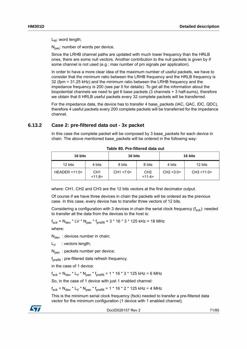
DocID026157 Rev 2 71/85
HM301D Detailed description
85
LW: word length;
Npac: number of words per device.
Since the LRHB channel paths are updated with much lower frequency than the HRLB ones, there are some null vectors. Another contribution to the null packets is given by if some channel is not used (e.g.: max number of pm signals per application).
In order to have a more clear idea of the maximum number of useful packets, we have to consider that the minimum ratio between the LRHB frequency and the HRLB frequency is 32 (fpm = 31.25 kHz) and the minimum ratio between the LRHB frequency and the impedance frequency is 200 (see par 0 for details). To get all the information about the biopotential channels we need to get 6 base packets (3 channels + 3 half-sums), therefore we obtain that 6 HRLB useful packets every 32 complete packets will be transferred.
For the impedance data, the device has to transfer 4 base_packets (IAC, QAC, IDC, QDC), therefore 4 useful packets every 200 complete packets will be transferred for the impedance channel.
6.13.2 Case 2: pre-filtered data out - 3x packet
In this case the complete packet will be composed by 3 base_packets for each device in chain. The above mentioned base_packets will be ordered in the following way:
where: CH1, CH2 and CH3 are the 12 bits vectors at the first decimator output.
Of course if we have three devices in chain the packets will be ordered as the previous case. In this case, every device has to transfer three vectors of 12 bits.
Considering a configuration with 3 devices in chain the serial clock frequency (fsck): needed to transfer all the data from the devices to the host is:
fsck = Ndev * LV * Npac * fprefilt = 3 * 16 * 3 * 125 kHz = 18 MHz
where:
Ndev : devices number in chain;
LV : vectors length;
Npac : packets number per device;
fprefilt : pre-filtered data refresh frequency.
in the case of 1 device:
fsck = Ndev * LV * Npac * fprefilt = 1 * 16 * 3 * 125 kHz = 6 MHz
So, in the case of 1 device with just 1 enabled channel:
fsck = Ndev * LV * Npac * fprefilt = 1 * 16 * 2 * 125 kHz = 4 MHz
This is the minimum serial clock frequency (fsck) needed to transfer a pre-filtered data vector for the minimum configuration (1 device with 1 enabled channel).
Table 80. Pre-filtered data out
16 bits 16 bits 16 bits
12 bits 4 bits 8 bits 8 bits 4 bits 12 bits
HEADER <11:0> CH1 <11:8>
CH1 <7:0> CH2 <11:4>
CH2 <3:0> CH3 <11:0>

Detailed description HM301D
72/85 DocID026157 Rev 2
6.13.3 Header description
The header packet contains the useful info to correctly interpret the whole packet meaning. The header packet is composed by 16bits in case 1 and by 12 bits in case 2:
Table 81. Header packet bits description in 4x packet case
Header bits Name Description Details
15:11 Not used
10 LRHB2_ENLRHB channel 2 data
enable
9 LRHB1_ENLRHB channel 1 data
enable
8:7 NUM_DEV <2:0>Number Devices in daisy
chain configuration
00: 1 device
01: 2 devices
10: 3 devices
11: 4 devices
6 PREFIL_EN Pre-filtered data out enable
5 PMD2LRHB channel 2 data
enable
4 PMD1LRHB channel 1data
enable
3:0 C_DATA_DESC <3:0> C_DATA description See Table 82
Table 82. Header packet bits description in 3x packet case
Header bits Name Description Details
11:9 Not used
8:7 NUM_DEV <2:0> Number Devices in daisy chain configuration
00: 1 device
01: 2 devices
10: 3 devices
11: 4 devices
6 PREFIL_EN Pre-filtered data out enable
5 LRHB2_EN LRHB channel 2 data enable
4 LRHB1_EN LRHB channel 1data enable
3:0 C_DATA_DESC <3:0> C_DATA description See Table 82

DocID026157 Rev 2 73/85
HM301D Detailed description
85
The C_DATA packet contains different data according to the C_DATA_DESC. This is valid only for 4x packet case because in 3x packet case just the channels data is provided and without any filtering.
When the C_DATA vector contains the contact check and overflow data, its 16 bits have the following meaning:
Table 83. C_DATA packet description bits configurations
C_DATA_DESC
[3:0] C_DATA content
0000 No useful data in C_DATA vector
0001 CH1_HRLB data
0010 CH2_HRLB data
0011 CH3_HRLB data
0100 NOT USED
0101 (CH1_HRLB + CH2_HRLB)/2 data
0110 (CH2_HRLB + CH3_HRLB)/2 data
0111 (CH3_HRLB + CH1_HRLB)/2 data
1000 ZC DC_I data
1001 ZC DC_Q data
1010 ZC AC_I data
1011 ZC AC_Q data
1100 Contact Check and overflow data (See Table 82)
1101 NOT USED
1110 NOT USED
1111 NOT USED
Table 84. Contact check and overflow C_DATA vector
Contact check and overflow C_DATA details [C_DATA_DESC=1100]
<15:0> Description
15:14 Not used
13 over_curr_p
12 over_curr_n
11:10 psmon
9 Impedance channel overflow
8 CH3 overflow
7 CH2 overflow

Detailed description HM301D
74/85 DocID026157 Rev 2
6.14 Data rate
The following two tables describe respectively the HRLB data-out sampling frequencies as function of the HRLB low pass filter cut-off frequency and the LRHB data-out sampling frequencies as function of the LRHB low pass filter cut-off frequency.
Also for the impedance channel the data rate is function of low pass filter cut-off frequency; Table 87 provides the two sampling frequencies as function of low pass filter cut-off frequency.
6 CH1 overflow
5 IN3N DC contact check
4 IN3P DC contact check
3 IN2N DC contact check
2 IN2P DC contact check
1 IN1N DC contact check
0 IN1P DC contact check
Table 84. Contact check and overflow C_DATA vector (continued)
Contact check and overflow C_DATA details [C_DATA_DESC=1100]
<15:0> Description
Table 85. HRLB data-out sampling frequency vs low pass filter cut-off frequency
CiaHRLB low pass fcut selector
[hc_dig_ecglpf_sel_r] in SET15 registerLow pass cut-off frequency (-3 dB)
Sampling frequency HRLB data out
1000 600 Hz 1.953 kHz
0000 300 Hz 0.976 kHz
0001 200 Hz 0.651 kHz
0010 150 Hz 0.488 kHz
0011 100 Hz 0.325 kHz
0100 75 Hz 0.244 kHz
0101 50 Hz 0.163 kHz
0110 37 Hz 0.122 kHz
0111 25 Hz 0.0815 kHz
Table 86. LRHB data-out sampling frequency vs low pass filter cut-off frequency
PM low pass fcut selector [hc_dig_pmlpf_sel_r] in SET 16 register
Low pass cut-off frequency (-3 dB)
Sampling frequency PM data out
0 10 kHz 31.25 kHz
1 5 kHz 15.625 kHz

DocID026157 Rev 2 75/85
HM301D Detailed description
85
6.15 Data ready operation
The HM301D has two types of data ready and SPI clock operation: packets data streaming and direct read command mode. These two procedures can be selected by Meas_mode bit of SET22 register (SET22 <7>).
One of the two ways can be used by choosing the proper signal as data ready in one of the DGIOs (refer to Table 11, Table 12 and Table 13). The packets data streaming method must be used if we are interested to retrieve the LRHB data; in this case the data ready signal to monitor is the pm_resh. If we are interested to read only the ECG data then the direct read command procedure must be selected and the data ready signal to monitor is the ecg_rsh.
Figure 21. SPI communication - packet data streaming
If Meas_mode bit is zero, the packets data streaming operation is selected. In case of complete processed data the packet is composed by 4 words of 16 bits and the SPI master must send at least 80 clock pulses only after the Pm_resh signal goes high. The first 16 pulses are used by the HM301D to shift the data into the SPI registers so SDO stays low. While with the other 64 clock pulses the MCU can retrieve the 64bits packet data (Figure 18).
In case of pre-filtered data, the operation is exactly the same except for the fact that the packet is composed by 3 words bits so, just 64 and not 80 bits should be supplied by the MCU. In this case the right signal to be used as data ready is the prefilt_rsh which is output on DGIO0 with DGIO0_muxsel_r=1010 and on DGIO1 with DGIO1_muxsel_r=1001.
In both cases the tDATA_RSHB is the set by the internal clock of the LRHB which can be 31.25 kHz or 15.625 kHz according to the low pass filter selection of the LRHB signal chain.
If just the HRLB signals are of interest, the data can be retrieved using the SPI data read command mode. To select this method the Meas_mode bit must be asserted. In this case
Table 87. Impedance data-out sampling frequency vs low pass filter cut-off frequency
Impedance low pass fcut selector [imp_dig_lpf_sel_r] in SET19 register
Low pass cut-off frequency (-3 dB)
Sampling frequency Impedance data out
0 1 Hz 7.8 Hz
1 20 Hz 156 Hz

Detailed description HM301D
76/85 DocID026157 Rev 2
the ecg_rsh must be used as trigger signal, so when ecg_rsh goes high the microcontroller must directly read the ECG_OUT registers using the direct word reading procedure as described in Figure 19. This ecg_rsh signal is available at DGIO2 with DGIO2_muxsel_r=1010.
Figure 22. ECG_OUT registers data reading
SPC
CS
32 bits
SDIR/W
AD6
AD5
AD4
AD3
AD2
AD1
AD0
R/W
AD6
AD5
AD4
AD3
AD2
AD1
AD0
SDOD7
D6
D5
D4
D3
D2
D1
D0
R/W
AD6
AD5
AD4
AD3
AD2
AD1
AD0
R/W
AD6
AD5
AD4
AD3
AD2
AD1
AD0
R/W
AD6
AD5
AD4
AD3
AD2
AD1
AD0
D7
D6
D5
D4
D3
D2
D1
D0
ECG_rsh

DocID026157 Rev 2 77/85
HM301D Application Information
85
7 Application Information
7.1 DC offset removal
The electrode half-cell potential acts as a DC offset voltage on each of the incoming electrode signals and, depending on the application, also on the outgoing RLD electrode signal. In the biopotential channels and in the impedance channel the DC component is removed by the high pass filters.
The maximum half cell potential (DC_OS) the device can handle is defined by the supply voltage and by the RLD reference voltage RLF_VREF. Since the DC value is removed at the inputs of each acquisition channel, the limiting building block is the output swing of the RLD buffer which is limited by the supply voltage. The output swing towards VSS is limited by the difference between VREF and VSS. The output swing towards VDD is limited by the difference between VDD and RLF_VREF.
The worst case situation is when all half-cell potentials are in the same direction, i.e. positive or negative. In this case from the RLD output buffer towards the input of the health channel two half-cell potentials have to be subtracted. According to the medical standard, the RLD has to deliver 880 nA peak current. This gives an additional voltage drop of 264 mV over the DC current limiting resistor of the RLD. So the maximum output swing the RLD node (after the internal resistor) is VSS+325 mV and VDD-350 mV.
Taking all signals into account, the maximum DC offset can be calculated as the minimum of the following two equations:
Equation 3
Equation 4
For higher VDD, DCOSVDD increases while DCOSVSS stays the same. So, at high VDD, it is beneficial to increase the RLD reference voltage RLD_VREF voltage in order to cope with higher DC offset. The bits rld_ref_sel_r change the RLD reference voltage to 0.7 V, 1.0 V and 1.49 V.
Figure 23 shows the maximal electrode offset versus supply for different reference voltages.
)325.0(_ VSSVREFRLDDCOSVSS
VREFRLDVDDDCOSVDD _)350.0(

Application Information HM301D
78/85 DocID026157 Rev 2
Figure 23. Maximum DC offset removal
7.2 Multi-chip configuration
In order to build a system supporting more than 3 biopotential channels, the HM301D can be used in a multiple chip configuration.
In this configuration the SPI will be configured as daisy chained SPI by connecting the data output of one device to the data input of another. The first and the last devices of the chain will be connected to the MCU. The maximum number of devices that can be connected together is 4.
One of the HM301D chip can be used as analog master in the system: it distributes the WCT signal, drives the shield and right leg and sends out its clock signal to the others. Figure 24 shows an example of 3 HM301D connected together for 12 leads ECG application.
AM17593v1
-0.4
-0.2
0
0.2
0.4
0.6
0.8
1
1.2
1.4
1.6 1.8 2 2.2 2.4 2.6 2.8 3 3.2 3.4 3.6
DC
offs
et [V
]
AVDD [V]
VREF = 0.7 V
VREF = 1.0 V
VREF = 1.49 V

DocID026157 Rev 2 79/85
HM301D Application Information
85
Figure 24. Example of chain connection: standard 12-lead ECG
In multi-chip configuration the data send and received by the MCU through the SPI are formatted in a different way compared to single chip configuration.
AM17594v2
CSSPCSDISDO
CKEXT
AVG
VREF
SD
RLD
WCT
IN2PIN2N
IN1NIN1P
CSSPCSDISDO
CKEXT
AVG
VREF
IN2PIN2N
IN1NIN1P
SD
RLD
WCT
IN3NIN3P
CSSPCSDISDO
CKEXT
AVG
VREF
IN2PIN2N
IN1NIN1P
SD
RLD
WCT
IN3NIN3P
MISOMOSISCKSS
L
LL
R
RL
V1
V4
V5
V6
V2
V3
SHIELD
HM301D
HM301D
HM301DMCU

Application Information HM301D
80/85 DocID026157 Rev 2
7.3 Supported ECG configurations
Even if designed for any type of biopotential acquisition, the HM301D is particularly suited to ECG systems. To address most possible applications, each channel of the HM301D can be connected to the electrodes either as bipolar or unipolar.
At the output of the channel, the bipolar configuration gives the difference between 2 electrodes. Otherwise, the unipolar configuration reads the difference between the single electrode voltage and a reference voltage (the internal reference or WCT from the same chip or from the master chip in a chain connection).
As an example the standard 12-lead electrocardiogram application is shown in Figure 24. It requires the measurement of 12 differential signals, exploiting 9 electrodes. 8 differential channels are obtained by cascading 3 HM301D. The master (IC in the top) is connected to the 3 limb electrodes using a bipolar connection for both channels. It provides a WCT signal, clock timing and drives the RL electrode. HM301D devices, configured as unipolar, measure all 6 chest electrodes with respect to WCT. Combining the resulting 8 outputs, all 12 standards leads can be evaluated.
Table 88. Common ECG configurations
Application Electrodes Connection Channels Device
Standards 12 leads ECG 9 + RL 2 Bipolar + 6 Unipolar 8 3x HM301D
Standards 12 leads ECG 9 + RL 9 Unipolar 9 3x HM301D
Interpolated 12 leads using a 6 wires cable
5 + RL 2 bipolar + 2 unipolar 4 2x HM301D
Interpolated 12 leads using a 6 wires cable
5 + RL 5 unipolar 5 2x HM301D
5 leads wire / EASI 4 + RL 2 bipolar + 1 unipolar 3 1x HM301D
5 leads wire / EASI 4 + RL 4 unipolar 4 2x HM301D
Einthoven’s Triangle 3 + RL 2 bipolar 2 1x HM301D
Einthoven’s Triangle 3 + RL 3 unipolar 2 1x HM301D
Rhythm 2 1 bipolar 1 1x HM301D
Automated External Defibrillator (AED)
2 1 bipolar 1 1x HM301D

DocID026157 Rev 2 81/85
HM301D Package mechanical data
85
8 Package mechanical data
In order to meet environmental requirements, ST offers these devices in different grades of ECOPACK® packages, depending on their level of environmental compliance. ECOPACK® specifications, grade definitions and product status are available at: www.st.com. ECOPACK® is an ST trademark.

Package mechanical data HM301D
82/85 DocID026157 Rev 2
Figure 25. Package outline for LGA 40L (6 x 6 mm)

DocID026157 Rev 2 83/85
HM301D Package mechanical data
85
Table 89. LGA 40L (6 x 6 mm) mechanical data
Symbol(mm)
Min. Typ. Max.
A1 0.810 0.900 0.960
A2 0.660 0.700 0.710
A3 0.150 0.200 0.250
D1 5.850 6.000 6150
E1 5.850 6.000 6150
L1 4.460 4.500 4.540
L2 4.460 4.500 4.540
N1 0.460 0.500 0.540
N2 0.210 0.250 0.290
M 0.060 0.100 0.140
P1 2.690 2.730 2.77
P2 2.690 2.730 2.77
T1 0.310 0.350 0.390
T2 0.310 0.350 0.390
d 0.210 0.250 0.290
K 0.050
Revision history HM301D
84/85 DocID026157 Rev 2
9 Revision history
Table 90. Document revision history
Date Revision Changes
01-Apr-2014 1 Initial release
11-Apr-2014 2 Updated order code Table 1 on page 1
DocID026157 Rev 2 85/85
HM301D
85
Please Read Carefully:
Information in this document is provided solely in connection with ST products. STMicroelectronics NV and its subsidiaries (“ST”) reserve theright to make changes, corrections, modifications or improvements, to this document, and the products and services described herein at anytime, without notice.
All ST products are sold pursuant to ST’s terms and conditions of sale.
Purchasers are solely responsible for the choice, selection and use of the ST products and services described herein, and ST assumes noliability whatsoever relating to the choice, selection or use of the ST products and services described herein.
No license, express or implied, by estoppel or otherwise, to any intellectual property rights is granted under this document. If any part of thisdocument refers to any third party products or services it shall not be deemed a license grant by ST for the use of such third party productsor services, or any intellectual property contained therein or considered as a warranty covering the use in any manner whatsoever of suchthird party products or services or any intellectual property contained therein.
UNLESS OTHERWISE SET FORTH IN ST’S TERMS AND CONDITIONS OF SALE ST DISCLAIMS ANY EXPRESS OR IMPLIEDWARRANTY WITH RESPECT TO THE USE AND/OR SALE OF ST PRODUCTS INCLUDING WITHOUT LIMITATION IMPLIEDWARRANTIES OF MERCHANTABILITY, FITNESS FOR A PARTICULAR PURPOSE (AND THEIR EQUIVALENTS UNDER THE LAWSOF ANY JURISDICTION), OR INFRINGEMENT OF ANY PATENT, COPYRIGHT OR OTHER INTELLECTUAL PROPERTY RIGHT.
ST PRODUCTS ARE NOT DESIGNED OR AUTHORIZED FOR USE IN: (A) SAFETY CRITICAL APPLICATIONS SUCH AS LIFESUPPORTING, ACTIVE IMPLANTED DEVICES OR SYSTEMS WITH PRODUCT FUNCTIONAL SAFETY REQUIREMENTS; (B)AERONAUTIC APPLICATIONS; (C) AUTOMOTIVE APPLICATIONS OR ENVIRONMENTS, AND/OR (D) AEROSPACE APPLICATIONSOR ENVIRONMENTS. WHERE ST PRODUCTS ARE NOT DESIGNED FOR SUCH USE, THE PURCHASER SHALL USE PRODUCTS ATPURCHASER’S SOLE RISK, EVEN IF ST HAS BEEN INFORMED IN WRITING OF SUCH USAGE, UNLESS A PRODUCT ISEXPRESSLY DESIGNATED BY ST AS BEING INTENDED FOR “AUTOMOTIVE, AUTOMOTIVE SAFETY OR MEDICAL” INDUSTRYDOMAINS ACCORDING TO ST PRODUCT DESIGN SPECIFICATIONS. PRODUCTS FORMALLY ESCC, QML OR JAN QUALIFIED AREDEEMED SUITABLE FOR USE IN AEROSPACE BY THE CORRESPONDING GOVERNMENTAL AGENCY.
Resale of ST products with provisions different from the statements and/or technical features set forth in this document shall immediately voidany warranty granted by ST for the ST product or service described herein and shall not create or extend in any manner whatsoever, anyliability of ST.
ST and the ST logo are trademarks or registered trademarks of ST in various countries.Information in this document supersedes and replaces all information previously supplied.
The ST logo is a registered trademark of STMicroelectronics. All other names are the property of their respective owners.
© 2014 STMicroelectronics - All rights reserved
STMicroelectronics group of companies
Australia - Belgium - Brazil - Canada - China - Czech Republic - Finland - France - Germany - Hong Kong - India - Israel - Italy - Japan - Malaysia - Malta - Morocco - Philippines - Singapore - Spain - Sweden - Switzerland - United Kingdom - United States of America
www.st.com