development of cryogenic x-ray detectors interests, resources and capabilities in spain l.fàbrega
TRANSCRIPT

Development of Cryogenic X-ray DetectorsDevelopment of Cryogenic X-ray Detectors
Interests, Resources and Capabilities in
SpainL.Fàbrega
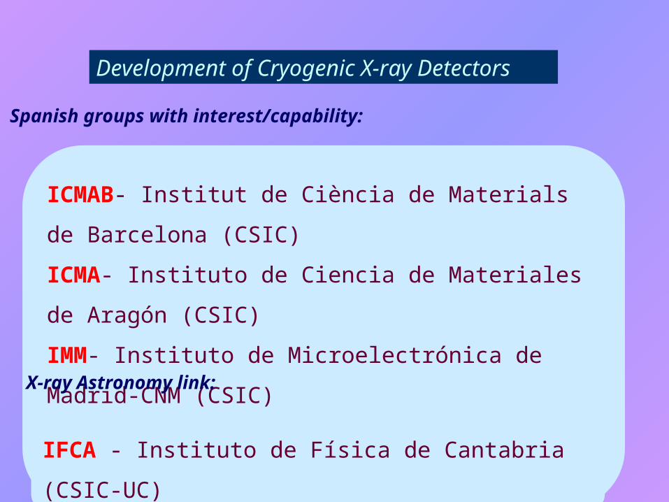
Spanish groups with interest/capability:
ICMAB- Institut de Ciència de Materials de Barcelona (CSIC)
ICMA- Instituto de Ciencia de Materiales de Aragón (CSIC)
IMM- Instituto de Microelectrónica de Madrid-CNM (CSIC)
IMB- Instituto de Microelectrónica de Barcelona-CNM (CSIC)
Development of Cryogenic X-ray Detectors
IFCA - Instituto de Física de Cantabria (CSIC-UC)
X-ray Astronomy link:

ICMAB: Dpt. of Magnetic and Superconducting Materials Epitaxial growth of oxide thin films and heterostructures Correlation structure/properties Superconductors: basic aspects and applications Devices with functional complex oxides:
Electro-optic modulators, tunable filtersMagnetic tunnel junctions
Main recent projectsFacilities
• AFM, SEM, TEM• XPS• Lithography
• THIOX (Thin films for novel oxide devices, ESF, 2002-06)
• SPINOX (New oxides and devices for telecommunications and magnetoelectronics, ESP, 2003-05)
• AMORE (Advanced Magnetic Oxides, UE, 2000-02)
• Oxide thin film technologies for superconducting and spintronic devices (ESP, 1999-2002)
•FAME (Functionalized advanced materials engineering, UE, 2004-)
Groups Expertise

Epitaxy: Characterization and control
1.0µm
0.0 0.20 0.40 0.60 0.80 1.0 1.2 1.4
0.0
1.0
2.0
3.0
4.0
5.0
6.0
7.0
X[µm]
Z[Å
]
SrRuO3 on SrTiO3
AFM
d = 6 nmLCMO
STO
HRTEM
ICMAB
0.25 0.50 0.75 1.00 1.25 1.50
10-4
10-3
10-2
10-1
100
(º)
R (
arb. unit
s)
Experimental data Fit
LCMO, 23.4nmLCMO, 23.4nm
DRX: Grazing Incidence Reflectometry

STO=18 m 28 m 43 m
325 m
1270 m1000 m
50 m
Magnetic tunnel junctions for spintronics: (La,Sr)MnO3/SrTiO3/ (La,Sr)MnO3
Project HEMAGE: ICMAB-IMM-ICMA
-20 -10 0 10 20
202
203
204
TMR 0.5 %?
R(
)
H(kOe)
10 K
RR RR
ICMAB

Wave guide
VRF
LiNbO3
• Lower losses• Higher speed
YBCO
Interface
YSZ
YBa2Cu3O7/YSZ/LiNbO3Projects COSMOS, MAT, SPINOX:
ICMAB-UPC-UB
Electrooptic modulators with superconductors: YBa2Cu3O7 on LiNbO3
ICMAB

Institute of Microelectronics of Madrid- IMM-CNM (CSIC) Dept. Fabrication and Characterization of Nanostructures
Electronic and optoelectronic devices, radiation detectors Magnetic tunnel junctions, Micro-SQUIDS, magneto-optics
Facilities:• UHV sputtering• EBL• MBE • RIBE
•AFM lithography
•Structural, magnetic and optical characterization of nanostructures
Recent main projects:
• NANOMAT (Growth 2001-2004)Self-assembled Nanostructured Materials for Electronic and Optoelectronic Applications
• MONA_LISA (BIO 2000-2003)Development of Novel Conjugated Molecular Nanostructures by lithography and their transport scaling aspects
• NANOMAGIQC (IST 2001-2004)Development of Superconducting circuits and microSQUIDS for the implementation of magnetic clusters based Qbits for Quantum Computing
• HIDEMAR (Growth 2002-2005)High Density nanopatterned Magnetic Recording Media
• NANOCIR (MCYT 2002-2005)Implantable Micro-and nanosystems for medical applications
Groups Expertise

InP
InP
SubstrateInP(001) (doped n+)
InP (doped n++)
InP (doped n+)
InP (doped p+)
InP(doped p++)
Waveguide:
Waveguide
QWR-1.55m
Waveguide SPS lattice match GaInAs/InP SPS GaInP/GaInAs
SubstrateGaAs
(doped n+)
GaInP (doped n++)
GaInP (doped n+)
GaInP (doped p+)
GaInP(doped p++)
Waveguide: GaAs
Waveguide: GaAs
QR-980nm
Project NANOMAT (IST 2001-2004)
Incorporation of self-organized quantum-wires and quantum rings in the active zone of laser diodes
IMM-CNM

sample
Vth
sample
Vox
adsorbed water
sample
x
MOx
dry N2
H2O vapor
Local Oxidation Nanolithography by AFM
250 nm 1 nm
20 nm 5 m
W = 45 nmSiO2
Au
Si
Au/Si
IMM-CNM

Detail of nanoconstrictions : 160 nm length, 35 nm wide.
Micro-SQUIDs fabricated by e-beam lithography at IMM-CSIC
- Dilution refrigerator measurements (spin tunnel and quantum coherence) UB
Project NANOMAGIQC (IST 2001-2004)
IMM-CNM

ICMA: Low Temperature Solid State Physics Department
Applications of SQUIDs and Josephson Junction devices Basic electronic aspects Magnetic and electric measurementsQuantum electrical metrology
Advanced scientific and technical instrumentation Cryogenics, very low temperatures (mK).
Facilities• Josephson Voltage Standard• Quantum Hall resistance Standard• SQUID based CCC for Quantum current standard• EUROMET (EC), CICYT, MIDAS• U. Twente, NMi, NPL, NIST
• VTI ( 9 T, 1.5 K-400 K)•3He (12T, 300 mK-10K)• Dilution ( 9 T, 20 mK-1 K)• Dilution ( 5 T, 10 mK-1 K)
Recent projects
Groups Expertise

10mK – 1K10mK – 1K5T5T
20mK – 1K20mK – 1K10T10T
300mK – 10K300mK – 10K12T12T
The Low Temperature labs The Low Temperature labs have been recently have been recently refurbrishedrefurbrished
ICMA

5 mm
ICMA
Voltage standard based on the Josephson effect
ICMA

1991:
JJ Voltage Standard is transfered from ICMA to
TPYCEA, Madrid
Uncertainty: 1 part in 108
1995:
QHE Resistance Standard to
TPYCEA
Uncertainty: 1 part in 109
2002: CCC-SQUID to Nmi, Holland
Uncertainty: 1 part in 1010
ICMA
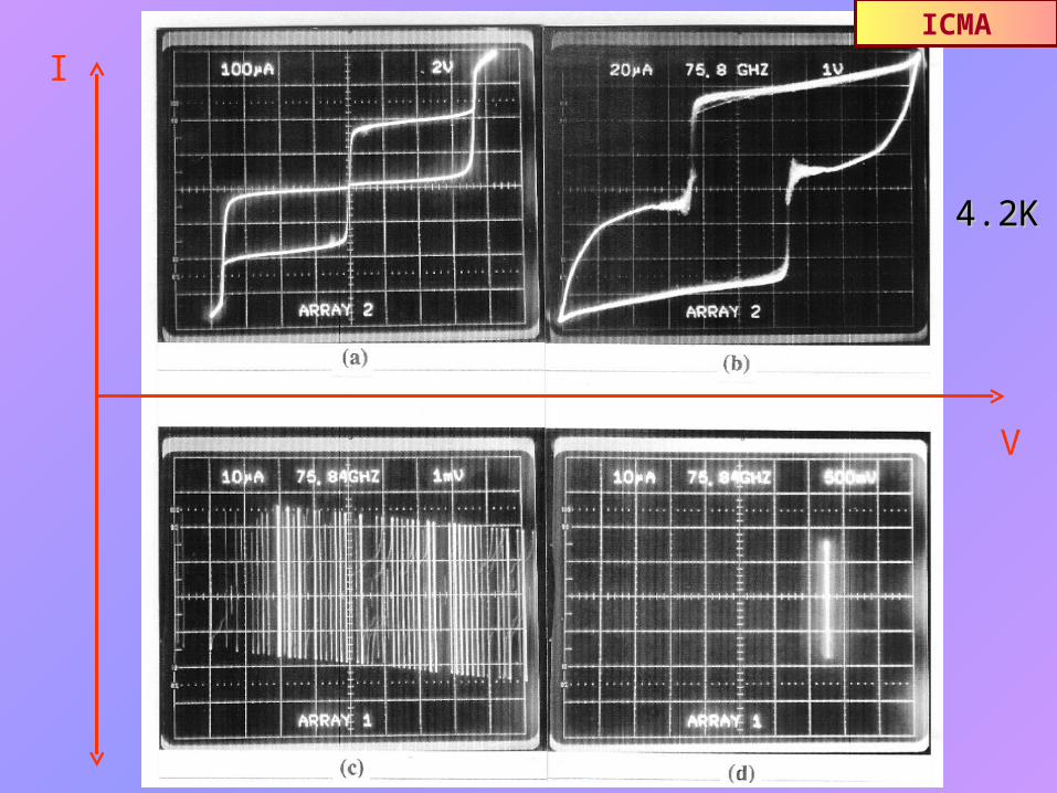
I
V
4.2K4.2K
ICMA

• Dpt. of Nanotechnology Nanolithography, Nanomechanics, Micro/nano systems for sensors
Processes available at the clean room
• Dpt. of Electronic circuits and systems design
Design, modeling and development of microsystems interfaces
• Clean Room 1.000 m2, CMOS Technology, Silicon technology, Micromechanics
• Wet and dry oxidations
• Ion implantation of B, P, As, N and Ar
• Diffusion (several ambients)
• CVD (nitride, polysilicon, oxide, BPSG)
• Metallization (Al-Si, Al-Cu, Al-Cu-Si, TaSi, Ti, Ni, Au*)
• Polyimide
•Wet and dry etching
• Surface and bulk silicon micromechanization
• Anodic bonding
• Packaging (die bonding, wire bonding, smd)
• Photolithography (proximity, step and repeat, double side)
•Nanolithography (e-beam, AFM, nanoimprint)
Institute of Microelectronics of Barcelona IMB-CNM (CSIC)
Groups Expertise
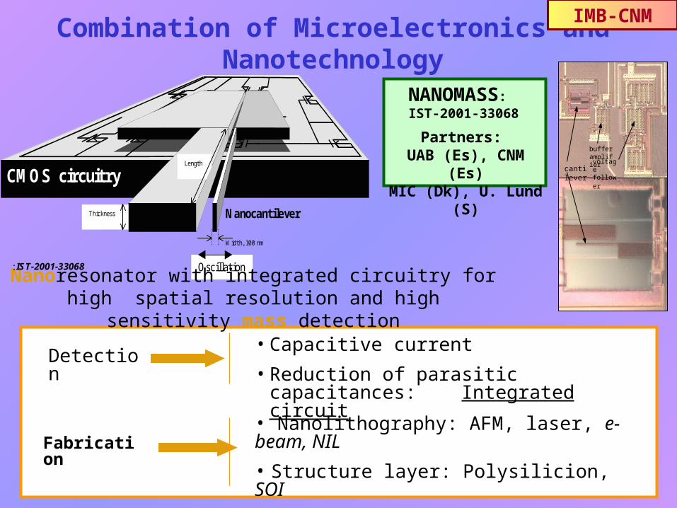
Combination of Microelectronics and Nanotechnology
Oscillation
Thickness
CMOS circuitry
Nanocantilever
Width, 100 nm
Length
Nanoresonator with integrated circuitry for high spatial resolution and high sensitivity mass detection
Fabrication• Nanolithography: AFM, laser, e-beam, NIL
• Structure layer: Polysilicion, SOI
• Combination with CMOS circuit fabrication
Detection• Capacitive current
• Reduction of parasitic capacitances: Integrated circuit
NANOMASS: IST-2001-33068
Partners: UAB (Es), CNM (Es)
MIC (Dk), U. Lund (S)
: IST-2001-33068
cantilever
buffer amplifier
voltage follower
IMB-CNM

Final implementation
ASICs, FPGAs, SoCs developmentASICs, FPGAs, SoCs development• Goals:
– SoC design for extreme environment applications.
– HDL based design methodologies.
– FPGA-ASIC retargeting/co-design.
• Techniques:– IP development with HDL languages
– Synthesis with EDA tools applicable to qualified technologies.
Projects:
SOCCER: SoC from Civilian to Armament Re-use. EUCLID-CEPA2, WEU/WEAO. MBDA (F), THALES Comunications (F), Galileo Avionica S.p.A. (I), CESVIT Microelecttronica SRL (I), SAAB Avionics (S), ASTRIUM - Crisa (E) & CNM-IMB (E). 2002-2005. NANOSAT: VLSI digital modem for LEO satellite communications, PNIE (CICYT), 1995-1997 (INTA (leader), ICM, UPM y CNM/UAB, y 1997-2000 INTA (leader), CNM-IMB & UPM).PEC-31750: Microcontroller for embedded space applications, ESTEC-ESA, 1994-96 (INDRA-Espacio (leader), TGI & CNM-IMB).PRENDA: Project for specification and normalisation on the design of ASICs, GAME (ESPRIT-CE), 1994-95 (Telefónica I+D (leader), Tecnológica, TGI, INDRA-Espacio, SIDSA, UPM-ETSII, UPM-ETSIT & CNM-IMB).
IMB-CNM

Microsystems integrationMicrosystems integration• Goals:
– MOEMS integration to build-up new -instruments for satellite applications.
– Study the use optical wireless links in order to reduce the size, weight and power consumption.
• Techniques:– Flexible MEMS architecture
– Integrated design methodology for MEMS
– IR diffused communication protocols & Optoelectronic devices qualification
Projects:• IDEA: Implementation of a Design Methodology for the Integration of microsystems in a distributed architecture (ESP).• OWLS: Study on Optical Wireless Systems for intra-satellite communications, ESTEC/ESA, 1999-2000 (INTA (leader), UPM & CNM-IMB)• Study of Interfacing Microdevices: Micro and Nanotechnologies considerations , ESTEC/ESA, 1998.
IMB-CNM

Dear Mama: New X-ray Imaging SystemDear Mama: New X-ray Imaging System
• Aim:– To develop a new mammography system based on
advanced photon solid state detectors and read-out circuits (ROIC)
– Advantages: Resolution&Contrast Dose (50 times less than film x-ray)
• Techniques:– Sensor BumpBonding to ROIC
– System based on an array (7*9) of {Sensor+ROIC}
– FPLD flexible control design
• Project: QLRT-2000-01318 (QoL-UE)
IMB-CNM
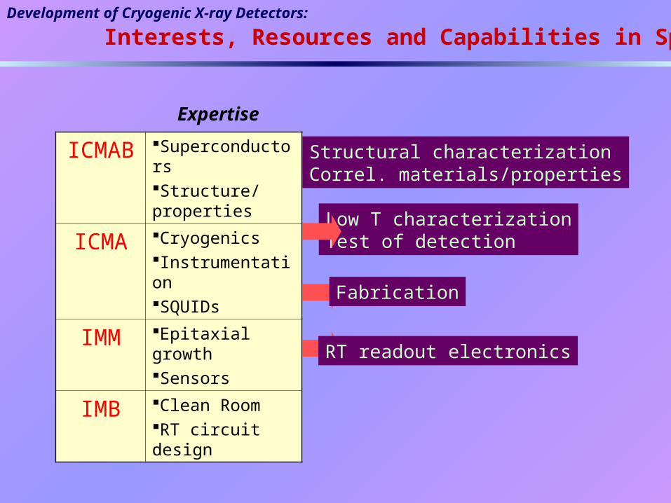
ICMAB SuperconductorsStructure/properties
ICMA CryogenicsInstrumentationSQUIDs
IMM Epitaxial growthSensors
IMB Clean RoomRT circuit design
Expertise
Structural characterizationCorrel. materials/properties
Fabrication
RT readout electronics
Low T characterizationTest of detection
Development of Cryogenic X-ray Detectors:
Interests, Resources and Capabilities in Spain


IMBIMB
New materialsNew materials
IMMIMM
IMBIMB
ICMABICMAB
ReadoutReadout
FabricationFabrication
Struct. charact.Struct. charact.ICMAICMA
TestTest
Development of Cryogenic X-ray Detectors:
Resources and Capabilities in Spain

Cryogenic detectors in Spain:
• Materials can be Fabricated
• Detectors could be Tested
• Detectors could be Developed
NOW
SOON
in the Future