development of an advanced semiconductor laboratory
TRANSCRIPT

Development of an Advanced Semiconductor Laboratory
Richard M. Bemben
Thesis submitted to the faculty of Virginia Polytechnic Institute and State University
in partial fulfillment of the requirements for the degree of
Masters of Science In
Electrical Engineering
Dr. Robert Hendricks, Co-Chairman
Dr. Kathleen Meehan, Co-Chairman
Dr. Joseph Tront
May 4, 2005 Blacksburg, Virginia
Keywords: Semiconductor processing; VTPMOS; advanced laboratory; course and curriculum development; L-Edit®; device design; device fabrication; device testing.

Development of an Advanced Semiconductor Laboratory
Richard M. Bemben
ABSTRACT Engineering faculty and administration at the Virginia Polytechnic Institute and State University (Virginia Tech) have recognized the importance of producing competent scientists and engineers to work in the vast semiconductor industry, especially in the emerging technologies of microelectronics, optoelectronics, and nanotechnology. For this reason, the development of an undergraduate microelectronics minor as well as a more rigorous graduate curriculum has been actively pursued for several years. This paper details the development of an advanced semiconductor processing laboratory course, which serves as a three credit hour capstone course. The course covers circuit layout, semiconductor fabrication, and electrical testing. The following steps were taken in order to accomplish this task: choosing and customizing a computer aided design (CAD) software package for device layout, pMOS process integration on the toolset in the cleanroom facilities at Virginia Tech, and the development of a laboratory manual.

Acknowledgements
I would like to acknowledge Dr. Robert Hendricks and Dr. Kathleen Meehan, who are co-chairs of my graduate committee. Dr. Hendricks provided me with the opportunity and funding to obtain my masters at Virginia Tech. Over the last 4 years he has been a teacher, a valued advisor, and a friend. Equally as important during my tenure at Virginia Tech has been my relationship with Dr. Meehan. She too has been a teacher, a valued advisor, and a friend. Also, her practical processing knowledge was invaluable while I developed the advanced processing laboratory course. Thank you both for direction you have given me. Next I would like to thank the eight students who participated in the first offering of this new laboratory course for permission to reproduce some of their data. Each is identified in the body of the thesis where their work is described. I would like to acknowledge my two roommates, Cyrus Karbassiyoon and Doug Linn, who I have lived with for several years. When I look back on my time at Virginia Tech, I will not remember the buildings or the classes; rather I will remember the relationships that I made. My experiences at Virginia Tech would have been incomplete without your friendships. Doug Linn is also the amateur photographer who took the digital photos in Appendix A. The old adage says to save the best for last, so finally I would like to acknowledge my family. When asked what my greatest strength is, I unfailingly respond that it is the love and support of my family. To mom, dad, and Lisa, knowing that you are always standing behind me has guided me through every accomplishment in my life. Thank you.
iii
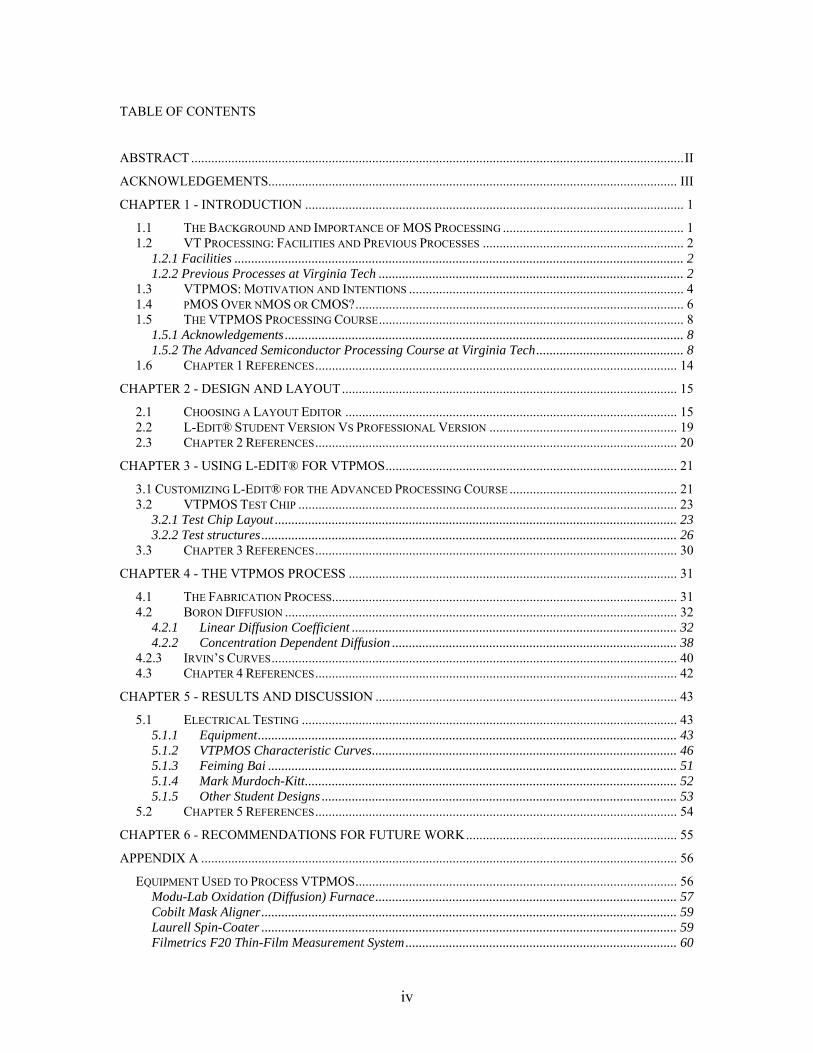
TABLE OF CONTENTS
ABSTRACT ...................................................................................................................................................II ACKNOWLEDGEMENTS.......................................................................................................................... III CHAPTER 1 - INTRODUCTION ................................................................................................................. 1
1.1 THE BACKGROUND AND IMPORTANCE OF MOS PROCESSING ...................................................... 1 1.2 VT PROCESSING: FACILITIES AND PREVIOUS PROCESSES ............................................................ 2
1.2.1 Facilities ...................................................................................................................................... 2 1.2.2 Previous Processes at Virginia Tech ........................................................................................... 2
1.3 VTPMOS: MOTIVATION AND INTENTIONS .................................................................................. 4 1.4 PMOS OVER NMOS OR CMOS?.................................................................................................. 6 1.5 THE VTPMOS PROCESSING COURSE........................................................................................... 8
1.5.1 Acknowledgements ....................................................................................................................... 8 1.5.2 The Advanced Semiconductor Processing Course at Virginia Tech............................................ 8
1.6 CHAPTER 1 REFERENCES............................................................................................................ 14 CHAPTER 2 - DESIGN AND LAYOUT.................................................................................................... 15
2.1 CHOOSING A LAYOUT EDITOR ................................................................................................... 15 2.2 L-EDIT® STUDENT VERSION VS PROFESSIONAL VERSION ........................................................ 19 2.3 CHAPTER 2 REFERENCES............................................................................................................ 20
CHAPTER 3 - USING L-EDIT® FOR VTPMOS....................................................................................... 21 3.1 CUSTOMIZING L-EDIT® FOR THE ADVANCED PROCESSING COURSE .................................................. 21 3.2 VTPMOS TEST CHIP ................................................................................................................. 23
3.2.1 Test Chip Layout ........................................................................................................................ 23 3.2.2 Test structures............................................................................................................................ 26
3.3 CHAPTER 3 REFERENCES............................................................................................................ 30 CHAPTER 4 - THE VTPMOS PROCESS .................................................................................................. 31
4.1 THE FABRICATION PROCESS....................................................................................................... 31 4.2 BORON DIFFUSION ..................................................................................................................... 32
4.2.1 Linear Diffusion Coefficient ................................................................................................. 32 4.2.2 Concentration Dependent Diffusion ..................................................................................... 38
4.2.3 IRVIN’S CURVES......................................................................................................................... 40 4.3 CHAPTER 4 REFERENCES............................................................................................................ 42
CHAPTER 5 - RESULTS AND DISCUSSION .......................................................................................... 43 5.1 ELECTRICAL TESTING ................................................................................................................ 43
5.1.1 Equipment............................................................................................................................. 43 5.1.2 VTPMOS Characteristic Curves........................................................................................... 46 5.1.3 Feiming Bai .......................................................................................................................... 51 5.1.4 Mark Murdoch-Kitt............................................................................................................... 52 5.1.5 Other Student Designs .......................................................................................................... 53
5.2 CHAPTER 5 REFERENCES............................................................................................................ 54 CHAPTER 6 - RECOMMENDATIONS FOR FUTURE WORK............................................................... 55 APPENDIX A .............................................................................................................................................. 56
EQUIPMENT USED TO PROCESS VTPMOS................................................................................................ 56 Modu-Lab Oxidation (Diffusion) Furnace.......................................................................................... 57 Cobilt Mask Aligner............................................................................................................................ 59 Laurell Spin-Coater ............................................................................................................................ 59 Filmetrics F20 Thin-Film Measurement System................................................................................. 60
iv

Optical Microscope............................................................................................................................. 60 Fischer Convection Oven.................................................................................................................... 61 Chemical Safety Gear ......................................................................................................................... 62 Wet Bench ........................................................................................................................................... 63 Electrical Test Station......................................................................................................................... 64
APPENDIX B............................................................................................................................................... 65 INSTALLATION AND STARTUP OF L-EDIT STUDENT V7.12........................................................................ 65
APPENDIX C............................................................................................................................................... 69 ADVANCED SEMICONDUCTOR PROCESSING LABORATORY MANUAL ....................................................... 69
VITA .......................................................................................................................................................... 106
v

LIST OF FIGURES
FIGURE 1 BREAKDOWN OF 15 WEEK SEMESTER FOR THE ADVANCED PROCESSING COURSE AT VIRGINIA TECH.
.............................................................................................................................................................. 9 FIGURE 2 VTPMOS PROCESS FLOW. THE ALTERNATING BLUE AND RED COLORS ARE LABORATORY DAYS
THAT THE STUDENTS MUST BE INVOLVED IN. YELLOW SIGNIFIES OPTIONAL OFFLINE PROCESSING DAYS THAT CAN BE COMPLETED BY THE TA DUE TO TIME CONSIDERATIONS. ............................................... 13
FIGURE 3 STANDARD PAD-FRAME USED IN THE ADVANCED SEMICONDUCTOR PROCESSING COURSE AT VIRGINIA TECH. REPRODUCED FROM RIT LECTURE NOTES .2 .............................................................. 22
FIGURE 4 MAP OF TEST CHIP ......................................................................................................................... 24 FIGURE 5 L-EDIT® LAYOUT SCREENSHOT OF THE TEST CHIP FABRICATED IN THE SPRING 2005 ADVANCED
SEMICONDUCTOR PROCESSING COURSE AT VIRGINIA TECH ................................................................. 25 FIGURE 6 L-EDIT® LAYOUT SCREENSHOT OF VERNIER ALIGNMENT MARKS.................................................. 26 FIGURE 7 L-EDIT® LAYOUT SCREENSHOT OF VAN DER PAUW SHEET RESISTANCE TEST STRUCTURES AND A
KELVIN CONTACT RESISTANCE TEST STRUCTURE ................................................................................ 27 FIGURE 8 L-EDIT® LAYOUT SCREENSHOT OF LINEWIDTH TEST STRUCTURES................................................ 29 FIGURE 9 ROOM-TEMPERATURE RESISTIVITY IN N AND P TYPE SILICON AS A FUNCTION OF IMPURITY
CONCENTRATION. REPRODUCED FROM JAEGER .3 ................................................................................ 34 FIGURE 10 SOLID SOLUBILITY CURVES FOR VARIOUS DOPANTS IN SILICON. REPRODUCED FROM PLUMMER .1
............................................................................................................................................................ 35 FIGURE 11 SPREAD SHEET OF POST-PREDEPOSITION CALCULATIONS............................................................. 36 FIGURE 12 SPREAD SHEET OF POST-DRIVE-IN CALCULATIONS....................................................................... 37 FIGURE 13 SPREADSHEET OF PREDEP CALCULATIONS USING CONCENTRATION DEPENDENT DIFFUSION
COEFFICIENT. ....................................................................................................................................... 39 FIGURE 14 IRVIN’S CURVE FOR P-TYPE CONSTANT-SOURCE DIFFUSION. REPRODUCED FROM JAEGER [3]. .... 40 FIGURE 15 IRVIN’S CURVE FOR P-TYPE LIMITED-SOURCE DIFFUSION. REPRODUCED FROM JAEGER [3]. ........ 41 FIGURE 16 I VS. V CHARACTERISTIC CURVE FOR MOSFET. REPRODUCED FROM [3].D DS ............................. 44 FIGURE 17 I VS. V CHARACTERISTIC CURVE FOR MOSFET. REPRODUCED FROM [3].D GS ............................. 44 FIGURE 18 TYPICAL DRAIN CHARACTERISTIC CURVES FOR RIT TRANSISTOR................................................ 45 FIGURE 19 THRESHOLD VOLTAGE CHARACTERISTIC FOR TYPICAL RIT TRANSISTOR..................................... 46 FIGURE 20 TYPICAL DRAIN CHARACTERISTIC FOR NON-FUNCTIONAL VTPMOS TRANSISTOR. ..................... 47 FIGURE 21 TYPICAL THRESHOLD VOLTAGE CHARACTERISTIC FOR NON-FUNCTIONAL VTPMOS TRANSISTOR.
............................................................................................................................................................ 48 FIGURE 22 TYPICAL DRAIN CHARACTERISTIC FOR FUNCTIONAL VTPMOS TRANSISTOR. ............................. 49 FIGURE 23 TYPICAL THRESHOLD VOLTAGE CHARACTERISTIC FOR FUNCTIONAL VTPMOS TRANSISTOR...... 50 FIGURE 24 (TOP LEFT) RESISTORS, (TOP RIGHT) SEVEN-CIRCLE PLANAR INDUCTOR, (BOTTOM)
INTERDIGITATED CAPACITOR. ALL OF THESE IMAGES WERE TAKEN FROM COURSE WAFERS. .............. 51 FIGURE 25 (LEFT) DIFFUSED RESISTORS (RIGHT) CONTACT RESISTANCE TEST STRUCTURE ............................ 52 FIGURE 26 SIDE CONTROL PANEL OF OXIDATION FURNACE. .......................................................................... 57 FIGURE 27 ENLARGEMENT OF TEMPERATURE CONTROLS. CENTER CONTROLLER IS SET TO DESIRED
TEMPERATURE AND OTHER CONTROLLERS ARE USED TO MONITOR THE TEMPERATURE AT THE FRONT AND BACK OF THE FURNACE. ............................................................................................................... 57
FIGURE 28 ENLARGEMENT OF FLOW METERS THAT CONTROL HOW MUCH NITROGEN AND OXYGEN ENTER THE FURNACE. ............................................................................................................................................ 58
FIGURE 29 BUBBLER SYSTEM TO ACCOMMODATE WET OXIDATIONS............................................................. 58 FIGURE 30 COBILT MASK ALIGNER................................................................................................................ 59 FIGURE 31 LAURELL SPIN COATER. USED TO SPIN PHOTORESIST, SPIN-ON BORON, AND TO CLEAN THE
WAFERS WITH ACETONE AND IPA........................................................................................................ 59 FIGURE 32 FILMETRICS F20 THIN-FILM MEASUREMENT SYSTEM. USED IN THE VTPMOS PROCESS TO
MEASURE OXIDE THICKNESSES. ........................................................................................................... 60 FIGURE 33 OPTICAL MICROSCOPE USED TO VERIFY ALIGNMENT. .................................................................. 60 FIGURE 34 CONVECTION OVEN USED IN BORON PREDEPOSITION. .................................................................. 61 FIGURE 35 PROPER USE OF CHEMICAL SAFETY GEAR. CHEMICAL SAFETY GEAR IS TO BE WORN WHILE
HANDLING HF AND ALUMINUM ETCH. ................................................................................................ 62
vi

FIGURE 36 WET BENCH. LEFT SIDE ACCOMMODATES PHOTORESIST DEVELOPER AND SOLVENTS. RIGHT SIDE ACCOMMODATES HF. .......................................................................................................................... 63
FIGURE 37 ELECTRICAL TEST STATION USED TO CHARACTERIZE DEVICES AS DESCRIBED IN GRAY’S THESIS.64 FIGURE 38 ENLARGEMENT OF 4-POINT PROBE STATION USED TO MEASURE SHEET RESISTANCE.................... 64
vii

LIST OF TABLES
TABLE 1 LAYOUT EDITOR COMPARISONS ...................................................................................................... 18 TABLE 2 EMPIRICAL MEASUREMENTS EXTRACTED FROM RIT PMOS PROCESS............................................. 33 TABLE 3 SHEET RESISTANCE MEASUREMENTS OF BORON DIFFUSION AFTER THERMAL PROCESSING FOR ...... 33 TABLE 4 EMPIRICAL AND THEORETICAL VALUES OF SHEET RESISTANCE AND JUNCTION DEPTH FOR THE
VTPMOS PROCESS AND THE RIT PMOS PROCESS. P = PREDEP, D1 = DRIVE-IN 1, D2 = DRIVE-IN 2. 37 TABLE 5 TABLE OF STUDENT DESIGNS........................................................................................................... 49
viii

Chapter 1 - Introduction
1.1 The Background and Importance of MOS Processing On March 7th, 1933, US. Patent No. 1,900,018 was awarded to Julius Edgar Lilienfeld for his efforts in creating an early version of the metal oxide semiconductor field effect transistor (MOSFET) on a cuprous sulphide substrate [1]. His choice of material, impractical design, and archaic processing techniques leave much to be desired by today’s high-tech silicon semiconductor manufacturing standards, but it had to start somewhere. A more structured proposal of the “field effect”, surface modulation of the conductivity of a semi-conducting material by the application of an electric field, was proposed in 1935 by Liandrat [2]. Unfortunately, transistor research and development was not aggressively pursed until William Shockley, Walter Brattain, and John Bardeen developed the point-contact transistor in 1947 [1], [2]. In the 1950’s and 60’s, the bipolar junction transistor (BJT) gained popularity over the MOSFET because the MOSFET suffered from surface problems and contamination issues [1], [2]. The development of a new fabrication technique, the planar process, in 1960 by Jean Hoerni, the introduction of the integrated circuit (IC) in 1958 by Jack Kilby, and increasing interest in digital computing deemed the MOSFET the transistor of choice and spawned the silicon era [1]. Today, semiconductors are a multi-billion dollar industry. The Wall Street Journal recently stated that the transistor drove the development of computers, satellites, space exploration, and much of modern communications and electronics [3]. In fact, the Semiconductor Industry Association (SIA) puts global semiconductor sales at over $166 billion in 2003 [4]. An industry of this size is very influential in the world economy and requires fresh, well-trained, scientists and engineers to maintain its growth.
1

1.2 VT Processing: Facilities and Previous Processes
1.2.1 Facilities Engineering faculty and administration at the Virginia Polytechnic Institute and State University (Virginia Tech) have recognized the importance of producing competent scientists and engineers to work in the vast semiconductor industry, especially in the emerging technologies of microelectronics, optoelectronics, and nanotechnology. For this reason, the development of an undergraduate microelectronics minor as well as a more rigorous graduate curriculum has been actively pursued for several years [5]. In order to adequately train the students and to accommodate the changing needs of the curriculum, an 1,800 ft2 class 10,000 cleanroom was constructed for laboratory experiment and semiconductor fabrication [6]. Briefly, the cleanroom is equipped with house vacuum, N2 and O2 distributed process gasses, and an 18.3 MΩ de-ionized water system. It contains several furnaces for oxidation and diffusion, mask aligners for feature alignment and photolithographic exposure, a wet etch and development station, wafer spinners, optical microscopes, and a thin film measurement system [6]. A detailed list with photographs of the equipment available is given in the Appendix A.
1.2.2 Previous Processes at Virginia Tech Previously, an elementary semiconductor processing course was available to undergraduate students from all breadths of engineering and the sciences in their sophomore year of studies. The only prerequisite was freshman chemistry. The processing course served as an introduction to silicon semiconductor processing and cleanroom etiquette/protocol [7]. Under the guidance of Dr. Robert Hendricks, David Gray and Christopher Timmons developed the procedures that were used in this elementary semiconductor processing course [8]. Gray later optimized several steps in the fabrication process to increase yield, which he documented in his graduate thesis [7]. A nine step nMOS process that required four photolithography masks was developed. Simple nMOS devices (resistors, p-n junctions, transistors, and simple circuits) were fabricated on 100 mm (4”) <100> Czochralski grown p-type silicon wafers that were generously donated by the Motorola Corporation. Layout was preformed in AutoCAD®
2

and followed 100 µm design rules. These AutoCAD® layouts were converted into photolithography masks, which were printed on standard transparencies using a high-resolution Alps MicrodryTM printer. While advanced students could easily fabricate and use their own mask sets, it was not a course requirement. Processing was broken into six 2-hour processing sessions, which collectively consisted of oxidation, diffusion, etching, photolithography, and physical vapor deposition (PVD). Students then performed electrical testing to characterize the nMOS devices that they fabricated [7], [8]. This course served as a solid introduction to electrical circuits and semiconductor processing and successfully educated students for several semesters. A more advanced fabrication process was proposed in a paper written in 2003 by Charles S. French, a Virginia Tech graduate student in materials science and engineering (MSE). He proposed an advanced semiconductor device laboratory for upper-level undergraduate students with electronics/microelectronics experience. French intended to process CMOS digital logic circuits [9]. CMOS logic requires more processing steps than the aforementioned nMOS process and is, therefore, more complicated. French outlined the specific process steps and developed a thermal budget, but the process was never reduced to practice. Processing CMOS logic would certainly be interesting and beneficial, but it is perhaps too ambitious for the toolset that Virginia Tech currently operates. Without ion implantation capabilities to accurately introduce and control the various impurities required, CMOS processing would be difficult, if not impossible. Also, the lack of chemical vapor deposition (CVD) capabilities means that only one layer of metallization is possible, limiting the number of possible logic circuits that could be created with CMOS logic. French also proposed using L-Edit®, a commercial computer aided design (CAD) layout package, to design the masks used to fabricate the devices (www.tanner.com). Feature size would be scaled down due to the fact that L-Edit® is capable of exporting GDS files, which can be used to fabricate a chrome-on-glass mask-set. Including this design phase into his advanced semiconductor processing lab, French estimated that it would span the first three weeks of the semester [9]. The remainder of the semester would be devoted to fabrication and analysis. This software package was intended to expose the students to a commercial CAD package focused on device layout and to benefit students who plan on working in the semiconductor industry.
3

1.3 VTPMOS: Motivation and Intentions An Interdisciplinary Curriculum for Microelectronics, written by several Virginia Tech faculty members, outlined an ambitious program for students to obtain an education in microelectronics [5]. Hands-on semiconductor processing and characterization experience is necessary to properly educate students in the microelectronics field. Yet, over the past few years, budget cuts have made it necessary to eliminate several courses that were identified in this program. The original undergraduate semiconductor processing laboratory course developed by Hendricks, Gray, and Timmons is one such course that is no longer offered. And as previously stated, French’s course development and process flow was only proposed and never reduced to practice. The end result is that Virginia Tech currently does not have a semiconductor processing laboratory course and the majority of the processing equipment lies dormant in the cleanroom. In an attempt to regain what was lost when the processing laboratory course was cut from the engineering curriculum, a new advanced semiconductor processing laboratory course has been proposed and developed. Acting as principle investigator, Dr. Robert Hendricks solicited one year of funding from the Micron Technologies Foundation, Inc. to accomplish the task of reinstating a processing laboratory course into Virginia Tech’s microelectronics curriculum. The advanced semiconductor processing laboratory course has several similarities as well as several differences compared with the previous processing laboratory course. Thus, a significant level of activity was required to establish this course. Similar to what Gray and Timmons developed, the new process for the advanced laboratory course is a multi-step fabrication process that requires four photomasks. Again, this process is capable of fabricating basic devices such as resistors, transistors, and simple circuits on 100 mm (4”) <100> Czochralski grown silicon wafers that were generously donated by the Motorola Corporation. Technically, the two processes are different because they fabricate different types of logic; nMOS logic circuits were fabricated in the previous course where pMOS logical gates are made during the new course processes. Therefore, the new course must fabricate devices on n-type wafers. Fabricating pMOS logic on n-type wafers alters the set of devices that can be fabricated, due to the limitation of the available processing equipment, and how the devices operate. The previous undergraduate course was intended to annually service 500 multi-disciplinary students [5], [7]. In contrast, this advanced processing course has an intended annual throughput of 15-30 senior-level undergraduate/first-year graduate
4

students who have cleanroom experience or theoretical processing knowledge from previous coursework and serves as a 3 credit hour capstone course. As previously stated, the undergraduate course served simply as an introduction to electronic circuits and semiconductor processing for students with little experience in these areas. Due to the fact that the new course targets experienced upper-level students, the new course can attain levels of sophistication that were not possible in the previous undergraduate course. In fact, it emphasizes three important concentrations within the integrated circuit (IC) manufacturing process. They are logic design and layout at the transistor level, pMOS fabrication, and post-fabrication testing to verify circuit operation. The characterization data obtained enables student to conduct an introductory-level failure mode analysis in which they can evaluate the impact of various fabrication steps on the device and circuit performance. Entire careers in various engineering disciplines have been devoted to a specific aspect of the IC manufacturing process such as IC design, fabrication, packaging, testing, and analysis. Clearly, students that plan a career in one of the aforementioned IC design/fabrication concentrations will benefit from the direct exposure they will receive in this new course. This course is also intended to be equally beneficial for students who do not plan a career in one specific concentration, but are contemplating a career elsewhere in the semiconductor/microelectronics industry. The exposure that these students will receive in this course will enable them to understand and to interact much more efficiently with the design engineers, process engineers, material scientists, and the test engineers, who are all equally important in creating a viable product for the market. Besides the differences in the teaching paradigm that were just mentioned, there are several other technical differences between the new laboratory course and the previous course. For instance, the fabrication process used in the new laboratory course is more sophisticated, where students design more complex logic circuits consisting of transistors with 10µm feature sizes. This is achieved by using a commercial CAD layout program and 10 µm design rules, which is the topic of Chapter 2. This CAD program creates files that can be read by commercial mask making systems and will be used to make a chrome-on-glass mask set. The mask set is then used in a mask aligner that has a resolution of 5 µm. Other differences include: the circuits designed in the new course are composed of pMOSFETs as opposed to the nMOS logic processed in the other course, a different diffusion method is utilized, and several equipment modifications were made. These technical differences will be the discussed and elaborated on in subsequent sections and chapters.
5

1.4 pMOS Over nMOS or CMOS? In an enhancement mode MOSFET the gate is insulated from the substrate by a thin dielectric. When a large enough voltage, the threshold voltage, is applied to the gate a channel is induced between the source and the drain. The channel is composed of carriers that are of the opposite type than the substrate, but they are same type as the source and drain. Then when a voltage is applied across the source and drain, current flows through the channel [10]. When the threshold voltage is applied to the gate of an enhancement mode nMOSFET, an n-type channel is induced in a p-type substrate. On the other hand, when the threshold voltage is applied to the gate of an enhancement mode pMOSFET, a p-type channel is induced in an n-type substrate. There are currently several thousand four inch p-type silicon wafers in storage at Virginia Tech that are ideal for fabricating nMOS logic. In contrast, there are about one hundred four inch n-type wafers in storage available that can be used to fabricate pMOS logic. Constraints on materials, tools, and other costs dominated many of the decisions made during the course of this project. But, despite the availability of wafers to fabricate nMOS logic, the current semiconductor processing course at Virginia Tech was designed around a pMOS process. The following discussion will detail several factors that influenced the decision to process and teach pMOS logic. First and foremost, my formal laboratory training in the field of semiconductor processing was undertaken at Rochester Institute of Technology (RIT). At RIT, I was taught their standard pMOS process that is used to instruct a 10 week undergraduate course. During this training, I became familiar with cleanroom etiquette and protocol, processing techniques, and their toolset. RIT’s willingness to collaborate with Virginia Tech as well as their consent to use, adjust, and/or modify their pMOS process was major motivation to teach pMOS logic. There were strict time constraints, which will be discussed in the following section, for having a process operational at Virginia Tech. Using RIT’s process as a foundation allowed process integration on Virginia Tech’s toolset in a timely manner. Thus, focus could be given to other areas such as choosing and customizing a CAD layout package. Another factor that influenced the decision to fabricate pMOS logic was the diffusion process. As mentioned previously as well as in Appendix C, which discusses the fabrication process in depth, Virginia Tech does not have the equipment to perform ion implantation. Ion implantation precisely introduces a specific dose of impurity (dopant) atoms into the substrate. The alternative methods for introducing impurity atoms are
6

from solid phase diffusion, gas phase diffusion, or using a liquid spin-on deposition source. The pros and cons of these three methods are discussed in Chapter 3, but it is suffice to say that all of these methods are limited to introducing dopants at or close to the substrate’s solid solubility level [2]. This means that the use of these methods will introduce the highest dose possible for a given substrate. Once a certain dopant dose is introduced into a substrate through a process known as pre-dep, the dopant atoms will diffused into the substrate. The spatial distribution of the dopant is determined by the magnitude of the dose and the temperature of the various high temperature thermal processes during and subsequent to the pre-dep. This is called limited source diffusion and the dopant concentration as a function of depth into the substrate generally follows a Gaussian distribution. But, the diffusion of dopants following doses of sufficiently high dopant concentrations, which is what must be dealt with in the the Virginia Tech process, exhibit non-Gaussian diffusion profiles. The diffusion becomes concentration dependent [11]. Regarding the decision to fabricate pMOS logic, high concentration boron diffusion profiles can be easily modeled, resulting in analytical relations between junction depth, sheet resistance, total dose, and surface concentration [11]. On the other hand, the high concentration phosphorous diffusion profile would have to be considered if we were fabricating nMOS logic. Gray’s thesis describes phosphorous diffusion in more detail because he used phosphorous to fabricate nMOS logic in the undergraduate laboratory that he helped develop. He states that phosphorous diffusion is still not fully understood due to unresolved/disputed aspects in the mode of diffusion, the diffusion coefficient, and the effect of precipitation of phosphorous in the silicon [7], [9]. For these reasons, the phosphorous profile is complicated and hard to model, analyze, and optimize. From this discussion, it is obviously advantageous to fabricated pMOS logic because the p-type dopant boron is easier to control, optimize, and analyze than the n-type dopant phosphorous.
7

1.5 The VTPMOS Processing Course The intention of this section is to describe the logistics and teaching objectives of the advanced semiconductor processing course at Virginia Tech. A course outline for a 15 week semester is described. Also, the process flow and laboratory breakdown are discussed and illustrated in Figure 1 and Figure 2.
1.5.1 Acknowledgements Collaboration between Dr. Karl Hirschman (Director of Semiconductor and Microsystems Fabrication Laboratory at RIT), Dr. Robert Hendricks of Virginia Tech, and the Micron Corporation afforded me the opportunity to spend the summer of 2004 working and training at RIT. While at RIT, I modified the layout of their pMOS test chip, learned cleanroom safety and protocol, learned their 10µm pMOS process, and learned how to process on their cleanroom toolset. After understanding the intricacies of the RIT pMOS process and the techniques used to process on their toolset, it was necessary to apply this knowledge with the toolset at Virginia Tech. I began to work on process integration in the fall semester of 2004. This required several process modifications as well as equipment modifications. The process modifications are detailed in Chapter 3 while the equipment modifications are discussed in Chapter 4.
1.5.2 The Advanced Semiconductor Processing Course at Virginia Tech The first objective of the advanced semiconductor processing course is to teach the students how to use the CAD layout software. Depending on how many students have taken courses in very large scale integration (VLSI) or have previous layout experience, the process of teaching the CAD software could take anywhere from one lecture to two weeks. Given the demographic of students that we are targeting for this course, more often than not there will be some students who are not experienced in layout. It is therefore necessary to estimate that two weeks are needed to prepare these students. In these two weeks, the CAD software is described and demonstrated in lecture sessions. Also, a description of the design rules is presented. Chapter 2 describes the details and idiosyncrasies of Tanner’s L-Edit®, the commercial CAD layout software that was chosen for use in the design phase of this course. Tanner maintains a student version of
8

L-Edit® downloaded and installed off of Tanner’s website (www.tanner.com). During the first two weeks students are encouraged to download and gain first-hand experience using the software. Following the first two weeks, the students are given an additional two weeks to design semiconductor devices and logic circuits, lay the devices out using the CAD software, and test (theoretically or through a simulation program such as SPICE) their designs. These designs must conform to the process’s design rules and are limited to a predefined amount of chip real-estate. For many students, these two weeks will be the most intense. A preliminary design is due at the end of the third week and the final designs are due at the end of the fourth week. Ultimately, these designs will be fabricated in the cleanroom and device performance comprises a large portion of the student’s grades. Therefore, these two weeks are very critical and it is necessary to actively participate/aid in the student’s designs to ensure that they are creating devices that can be realized by the VTPMOS fabrication process. At the end of the fourth week of the semester, all student designs are submitted to the course teaching assistant (TA). The TA then combines all of the designs into a single layout file using the professional version of L-Edit® (discussed in Chapter 2). The layout is converted into a file in GDS format, which is universally read by mask-making machines in order to fabricate photomasks. The GDS file is then sent off to a vendor who creates chrome-on glass photomasks specific to the designs encapsulated in the GDS file. The expected turn-around time for the vendor to fabricate the photomasks is one week. The week that is designated for the vendor to fabricate the photomasks is not lost time. Cleanroom safety/protocol and several processing steps can be performed before photomask 1 is needed. Therefore, the first laboratory session is held during the fifth week of the semester. The objective of the first lab is to introduce cleanroom safety/protocol and to prepare the course wafers for the first photolithography step. Please refer Figure 2 and Appendix C for more detail about the process steps accomplished in laboratory session 1.
Layout Fabrication Testing/Writing
Figure 1 Breakdown of 15 week semester for the advanced processing course at Virginia Tech.
1 2 3 4 5 6 7 8 9 10 11 12 13 14 15
9

As seen in Figure 1, there are seven scheduled laboratory sessions. Therefore, weeks five through eleven are dedicated to processing and related laboratory work. The last four weeks of the semester are dedicated to electrical testing and analysis, and to allow the students time in which they compile their final report, which details their devices through the entire layout/design, fabrication, and testing process. The duration of time dedicated to design, fabrication, and testing is illustrated for a 15 week semester by Figure 1.
10

4-Pt. Rs Probe(Predep)
Oxide Etch toremove boron
Boron Predep
Acetone RinseSpin Boron
Strip Resist
Lithography Mask #1
Oxide Etch (Active Area)
5000 Å OxideGrowth
Acetone/IPA Rinse
4-Pt. Rs Probe(Bare wafer)
Laboratory 1
Laboratory 2
Laboratory 3
11

Strip Resist
Oxide Etch (Contact Area)
Lithography Mask #3
Acetone Rinse
Gate Ox (Dry)Growth
Oxide Etch (Gate Area)
Strip Resist
Lithography Mask #2
Acetone/IPA Rinse
5000 Å OxideGrow/Measure
TA Processing
Laboratory 4
TA Processing
Laboratory 5
12

Acetone Rinse
Figure 2 VTPMOS process flow. The alternating blue and red colors are laboratory days that the students must be involved in. Yellow signifies optional offline processing days that can be completed by the TA due to time considerations.
Sputter Al
Lithography Mask #4
Al Etch
Strip Resist
Laboratory 6
Laboratory 7
Test & Analyze
13

1.6 Chapter 1 References [1] R. G. Arns, “The other transistor: early history of the metal-oxide-semiconductor field-effect transistor,” Engineering Science and Education Journal, vol. 7, issue 5, Oct. 1998. [2] J. D. Plummer, M. D. Deal, and P. B. Griffin, Silicon VLSI Technology Fundamentals, Practice and Modeling. Upper Saddle River, NJ: Prentice Hall, 2000, ch. 1&7. [3] C. Rhoads, “AT&T inventions fueled tech boom, and its own fall,” The Wall Street Journal, vol. CCXLV, no. 23, Feb. 2, 2005. [4] Semiconductor Industry Association. (1994-2003) Total Semiconductor World Market Sales & Share. Available: https://www.sia-online.org/downloads/market_shares_94-present.pdf [5] R. W. Hendricks, L. J. Guido, J. R. Heflin, and S. Sarin, “An interdisciplinary curriculum for microelectronics,” Proceedings of the 2001 ASEE Annual Conference & Exposition, June 24--27, 2001, Albuquerque, NM, Session 1526, Available: http://www.asee.org/acPapers/00580_2001.PDF [6] R. W. Hendricks, “An undergraduate microchip fabrication facility,” Proceedings of the 2001 ASEE Annual Conference & Exposition, June 24--27, 2001, Albuquerque, NM, Session 1332, Available: http://www.asee.org/acPapers/01054_2001.PDF [7] D. Gray, “Optimization of the process for semiconductor device fabrication in the MicrON 636 Whittemore cleanroom facility,” M.S. Thesis, Dept. MSE, Virginia Tech, Blacksburg, VA, 2002. Available: http://scholar.lib.vt.edu/theses/available/etd-08152003- 103345/unrestricted/fianlvers4.pdf [8] C. T. Timmons, D. T. Gray, and R. W. Hendricks, “Process development for an undergraduate microchip fabrication facility,” Proceedings of the 2001 ASEE Annual Conference & Exposition, June 24--27, 2001, Albuquerque, NM, Session 2464, Available: http://www.asee.org/acPapers/00808_2001.PDF [9] C. S. French, “Process development and planning for an advanced semiconductor device fabrication laboratory,” unpublished.
[10] A. R. Hambley, Electronics. Upper Saddle River, NJ: Prentice Hall, 2000, ch. 5. [11] R. C. Jaeger, Introduction to Microelectronic Fabrication Volume V. Reading, MA: Addison-Wesley Publishing Company, 1998.
14

Chapter 2 - Design and Layout
2.1 Choosing a Layout Editor Computer aided design (CAD) software packages are very important tools in the design of ICs. CAD software packages used in the IC industry allow users to design, test, and simulate electronic circuits and semiconductor devices before fabrication begins. Like other sophisticated design processes, there are several layers of abstraction in the IC design hierarchy. In general, the hierarchy begins at the behavioral level, and then advances to the RTL level, then to the logic level, then to the structural level, then finally to the layout level [1]. A circuit designer can start the design process from different levels depending on the complexity of the design [1]. As discussed in Chapter 1, the 15-week advanced semiconductor processing laboratory course dedicates four weeks to IC layout and design, in which devices with a minimum feature size of 10 µm are created. Creating photomasks with transparencies and the Alps MicrodryTM printer that were used in the previous undergraduate processing course can not accommodate designs at this feature size. Chrome-on glass photomasks can accommodate 10µm features cost-effectively and were chosen for use in the advanced processing course. Therefore, prior to offering this course, it was necessary to choose a CAD software package capable of exporting layout files in order to fabricate photomasks. For the purposes of this advanced processing course, the designs are expected to be simple enough to begin designing at the layout level. Choosing the lowest level of abstraction as the design environment for this course is beneficial because it will allow the students to understand their designs at the most basic level. Once they are comfortable with low level design of simple structures, they can design more complex devices using advanced tools in advanced VLSI courses such as ECE 4540. Therefore, a minimum requirement for the CAD software package is a layout editor. There are many sophisticated CAD packages available for IC design. The software package chosen for use in the advanced processing course needed to fulfill these following requirements:
1. It must be cost effective. The software license can not exceed the limited budget that the microelectronics funding reserves for design tools.
15

2. It must have a basic layout program which can be customized to the VTPMOS process. This customization includes the capability to create and manipulate process files.
3. Students using this software package in the processing course must be able to learn the software and produce mask ready designs in three to four weeks. Therefore, the user interface must be conducive to a fast learning environment.
4. Due to the fact that this software could and will be used in other courses, as well as in future research and development, ongoing vender support is required. Choosing a software package whose future is uncertain is risky. If discontinued, the time and effort spent learning the intricacies of the particular package would be lost.
5. Speed of integration. The software package must be installed, operational, and the appropriate people must be trained in two to three months.
The following additional considerations were made in choosing the appropriate CAD software package:
1. If possible, the students should be able to obtain copies of either a student version or a professional version of the software so that they can install the package on their home computers.
2. Due to the fact that the majority of students regularly work in a Windows® environment, it is preferred that the software package be Windows® compatible.
3. If licenses are limited by the software vendor, it is preferred that the licenses be allocated by a license server as opposed to license dongles.
4. The layout program should be able to write Spice netlists so that the layouts can be simulated and analyzed in Spice-compatible software.
With these requirements and constraints in mind, three software packages were analyzed. Two of the software packages that were under consideration are commercially available: Laker 2 from the Silicon Canvas Corporation and L-Edit® from Tanner EDA. The third layout package is freeware: LASI by Dr. D. E. Boyce. L-Edit® and Lasi were personally tested for about one day each. Laker 2 was never personally tested, rather several faculty and students met with a software representative from Silicon Canvas for several hours in order to gain insight into that software package. Table 1 compares and contrasts these three software packages based on the most important constraints for the advanced processing course. After careful consideration, L-Edit® was chosen for use in the advanced processing course. There are several aspects of L-Edit® that make it an attractive software package
16

for our needs. First, the user interface is very similar to Microsoft® Paint, which is a very straight forward and intuitive application. The assumption is that many students have had experience with Paint and can quickly adapt to using L-Edit®. Regardless, L-Edit® has the simplest and most intuitive user interface of the three software packages evaluated. Another attractive aspect of L-Edit® is the fact that Tanner offers a free student version that can be downloaded from their website. This is mutually beneficial for the students as well as the faculty and staff administering the course. It enables students to obtain their own copy of the software that they can learn, use, and customize at their leisure. It also reduces the overhead, i.e. workstations and software licenses, required to be maintained by the university.
17

Table 1 Layout editor comparisons
Laker (Silicon Canvas) [2]
L-Edit (Tanner EDA) [3]
LASI (Dr. D. E. Boyce) [4]
Cost Professional version: Low cost
Student version: Free Professional version: Low cost
All versions: Free
OS Unix based Windows based Windows based
Capabilities
- Layout tool with polygon editor -“Magic Cell” advanced device model (i.e. levels of hierarchy) - Interactive DRC/Error viewer.
- Extraction of Spice netlist from layout - Can be used by T-Spice circuit analyzer - Layout is similar to Microsoft® Paint. - Can customize layout environment for our process (i.e. choose visible layers and toolbars)
-Extraction of Spice netlist from the layout using “LasiCkt” command. - Netlists are compatible with HSpice, PSpice, and WINSpice. - “LasiCkt” command is process independent and process specific parameters must be updated in the Spice device models manually.
Limitations -Overly complex for VTPMOS
-Student version cannot produce GDS files
-Complex interface -No vendor support
Support from Publisher
Founded in 2001, Silicon Canvas is a relatively new corporation that is aggressively pursuing the custom layout market. Ongoing support is expected.
Tanner has been around for more than a decade (founded in 1988). Our contact is Wendy Knight and ongoing support is expected.
Due to the fact that the software and website are both authored and maintained by Dr. D. E. Boyce, ongoing support is questionable.
Manual & Help Menu
Adequate help menu and support from the vendor.
The student version comes with several .pdf files that are moderately helpful. Software package lacks good manual.
Cannot be searched by keyword, making it difficult to find answers to specific questions. Index is not helpful.
User Interface
Too complex for the limited window of time the students will have to learn the software.
Intuitive layout menu. Similar to Microsoft® Paint.
Layout menu confusing and overwhelming. Interface not conducive to rapid learning environment.
18

2.2 L-Edit® Student Version Vs Professional Version The student version of L-Edit® has certain intentional limitations that reduce its functionality compared to professional version. The most critical limitation is that the student version cannot convert layout files into GDS format. GDS format is a standardized format that mask-making machines read in order to write photomasks. The professional version of L-Edit® is required to export GDS files. Due to the fact that all student work is done in the student version, Virginia Tech is only required to maintain one copy of L-Edit® Pro to be used by the course teaching assistant. Therefore, using the L-Edit® software package cost effective. In order for TDB files to be compatible with both the professional version and the student version of L-Edit®, they must be developed in the student version. This is an important point because the student version is compatible with the professional version, but the professional version is not backward compatible with the student version. Therefore, any designs created in the professional version cannot be viewed or manipulated in the student version.
19

2.3 Chapter 2 References
[1] N. H. E. Weste, K. Eshraghian, Principles of CMOS VLSI Design: A System Perspective. Reading, MA: Addison-Wesley, 1993, ch. 6. [2] http://www.sicanvas.com/index-3.jsp [3] L-Edit Online User Guide, Tanner Research Inc., Pasadena, CA, 1998. Available: http://www.tanner.com/EDA/products/ledit/student_version.htm [4] http://members.aol.com/lasicad/candr.htm
20

Chapter 3 - Using L-Edit® for VTPMOS
3.1 Customizing L-Edit® for the Advanced Processing Course The paradigm used in the advanced processing course to create a final test chip design is that first the students create their individual designs using L-Edit® student and then submits them to the course teaching assistant (TA). The TA, who has access to L-Edit® Pro, combines all of the designs and any other appropriate test structures into one test chip. Using L-Edit® Pro, the TA then converts the test chip layout to GDS format and sends the file to a vendor to fabricate photomasks. For the purposes of this course, several additional files that are specific to the VTPMOS process were developed. The function of these files is to customize the user interface of the layout program to the four photomask pMOS process that is fabricated in the advanced processing course. Specifically, there are three additional files: VTPMOS_PadFrame.tdb, VTPMOS.xst, and L-Edit Installation-Setup-Startup.pdf. The first custom file listed above is VTPMOS_PadFrame.tdb. Notice that it has a TDB file extension. This file extension signifies a Tanner Database file which is a proprietary, machine-readable format used in the Tanner Tools environment [1]. TDB files contain layout designs and setup information such as layer-rendering information, GDS setup information, design rules, and configuration settings [1]. Therefore, this file contains the custom settings for the VTPMOS process. Importing the VTPMOS_PadFrame.tdb file will import the custom settings for the VTPMOS process. Setups are imported by executing File Replace Setup and choosing the appropriate TDB file [1]. Once VTPMOS_PadFrame.tdb is imported, users will be able to layout IC designs using four layers: Boron Diffusion, Gate Oxide, Contact Cut, and Aluminum. These four layers correspond to the four photomasks that are used in the VTPMOS fabrication process. The file VTPMOS_PadFrame.tdb also contains the layout of the pad frame which the student designs are required to use. These pads serve as electrical test pads and are therefore fabricated with the Aluminum layer. The design of the pad frame itself was developed at RIT [2]. It is a 12 pad layout, two rows of six pads separated by 500µm. Each pad is 100µm x 100µm and the pads are separated by 20µm. The area available between the two pad frame rows, which is the area designated for student designs, is
21
700µm x 500µm. A screenshot of the pad frame used in the advanced processing course is displayed in Figure 3. VTPMOS.xst is the second file designed to customize the user interface. The XST file extension signifies a cross-section definition file [1]. Cross-section definition files are used to enable the functionality of the Cross-Section option found in the Tools menu. Due to the fact that various engineering disciplines view devices and components in different ways, the capability to translate layout design into a device cross-section is an important visualization tool. It should be noted that this XST file is not to scale; it exaggerates certain processing steps, such as the gate oxide growth, so that the user can recognize that the process has occurred.
Figure 3 Standard pad-frame used in the advanced semiconductor processing course at Virginia Tech.
Reproduced from RIT lecture notes2.
Finally, the L-Edit Installation-Setup-Startup.pdf file is an instructional document. It details how to install L-Edit, how to import the VTPMOS custom setup, and how to utilize the VTPMOS.xst cross-sectional viewer. The contents of this file can be found in the appendix.
22

3.2 VTPMOS Test Chip
3.2.1 Test Chip Layout The layout of the test chip used in the advanced semiconductor processing course at Virginia Tech was originally developed at RIT. RIT has a standard pMOS process and maintains the layout of the pMOS test chip that is fabricated using its pMOS process [3]. Collaboration with RIT allowed Virginia Tech to use this pMOS test chip layout as the framework for the test chip to be fabricated in the advanced processing course. The test chip is divided into an 8 x 8 square grid. Each square is 800 µm x 800 µm, yielding a total test chip area of 6400 µm2. Pad-frames, as described in the previous section, are placed in these squares and layout occurs in the design space as illustrated in Figure 3 above. Under the direction of Dr. Karl Hirschman and Dr. Lynn Fuller, both professors in the Microelectronic Engineering Department at RIT, the test chip layout was updated in the summer of 2004. The layout was updated to include an array of transistors. The array of transistors consists of transistors with varying channel lengths and widths. From this array, one can determine the minimum channel length and width that yield functional transistors for a given fabrication process [4]. Also, several process parameters can be extracted by comparing electrical tests preformed on transistors of various sizes [5]. More detail on testing and test structures will be given in Section 3.2.2 and in Chapter 4. The test chip layout was also updated in order to accommodate student designs. The entire periphery of the 8 x 8 square grid, which accounts for 27 800 µm x 800 µm squares, was made available for student designs. Depending on the class size, it is feasible that each student be assigned several squares in order to layout multiple devices. Aside from the student designs and the transistor array, alignment marks, test structures, and digital logic occupy the remaining test chip area. The alignment marks serve to align each photomask level to the previous photomask level [6]. For example, the alignment mark on the second photomask is used in order to align to the first level. The test structures serve to characterize the fabrication process and extract process paramters. As mentioned, more discussion on test structures can be found in Section 3.2.2. Finally, the digital logic consists of simple devices such as inverters and nand/nor gates. Device complexity is limited by the fact that the fabrication process only uses one level of metallization. Figure 4 is a color coded map of the test chip. Figure 5 is a screen shot of
23

the actual test chip that was fabricated in the spring 2005 advanced semiconductor processing course at Virginia Tech. Note that when looking at L-Edit® layout screenshots green signifies boron diffusion, red signifies gate oxide, black signifies contact cut, and blue signifies aluminum metallization.
Test Chip
Key
Student Designs
Transistor Array
Test Structures
Alignment Marks
Digital Logic
Figure 4 Map of test chip
24

a b c d e f g h
1
2
3
4
5
6
7
8
Figure 5 L-Edit® layout screenshot of the test chip fabricated in the spring 2005 advanced semiconductor processing course at Virginia Tech
25

3.2.2 Test structures As seen in Figure 4, the test chip has four squares dedicated to test structures. The purpose of this section is to describe what the test structure are and how they can be used. This section does not provide data and analysis of electrical measurements. Refer to Chapter 4 for data and analysis of electrical measurements. The first test structure square (e4) contains horizontal and vertical alignment verniers as seen in Figure 6. One can determine photomask misalignment using these verniers by studying how the teeth of the two different layers align. When the center teeth align perfectly, then there is no misalignment. If the center teeth do not align, finding the teeth that are aligned and then counting the number of teeth away from the center (multiplied by the step size) yields the misalignment [7]. The step size for this design is one micron.
Figure 6 L-Edit® layout screenshot of vernier alignment marks
26

The second test structure square (b6) contains two Van der Pauw structures and one Kelvin structure. The Van der Pauw structures measure sheet resistance while the Kelvin structure measures contact resistance. Figure 7 is a screenshot of these structures.
1 2
4 3
Figure 7 L-Edit® layout screenshot of Van der Pauw sheet resistance test structures and a Kelvin contact resistance test structure
Jaeger describes Van der Pauw’s method on page 73 of ref. [6]; the sheet resistance of an arbitrarily shaped sample of material may be measured by placing four contacts on the periphery of the sample, injecting a current through one pair of contacts and measuring the voltage through the other pair of contacts. The test structure labeled VDPAUW1 in
27

Figure 7 is the arbitrary shaped diffusion layer described in Jaeger. The test structure labeled VDPAUW2 is the Greek cross structure. According to Walton, using the Greek cross structure yields sheet resistance accuracy better than 0.1% [8]. The intention of using multiple designs is to compare and contrast boron diffusion layer sheet resistance values obtained from the designs as well as the value obtained using the 4-point probe technique described in Gray [9]. The Kelvin structure is labeled CBKR in Figure 7. Notice that the pads are labeled 1-4. As detailed in ref. [8] and ref. [10], the method used in order to obtain the contact resistance is:
1. Force current between pads 1 and 3 and measure the voltage between pads 2 and 4.
2. Reverse the current between pads 1 and 3 and measure the voltage between pads 2 and 4.
3. Force current between pads 2 and 4 and measure the voltage between pads 1 and 3.
4. Reverse the current between pads 2 and 4 and measure the voltage between pads 1 and 3.
5. Average the four resistance values obtained from steps 1-4 which is labeled . cR
6. Calculate the contact resistivity using the formula, ARcc =ρ , where A is the
contact area in units of cm2 and cρ is the specific contact resistance in units of
ohm-cm2 [10].
The third test structure square (b7) contains two simple designs that are used to measure linewidth. It is important to measure linewidth in order to characterize etch uniformity of metal layers as well as lateral diffusion of dopants8. As can be seen in Figure 8, there is one structure used for measuring aluminum and one used for measuring boron diffusion. As detailed in [8], the method used to measure linewidth is:
1. Pass current between the two outer pads and measure the voltage between the two inner pads.
2. Calculate the resistance, , from the values in step 1. 1R
3. Calculate the linewidth from the equation,LR
RWs
1= , where is the sheet
resistance and is the length.
sR
L
28

Figure 8 L-Edit® layout screenshot of linewidth test structures
The fourth test structure square (c7) contains minimal sized transistors, for the VTPMOS process that refers to a channel length and width of 10 µm, that can be used to make measurements described in ref. [5]. Briefly, [5] describes a 30 measurement extraction process that is capable of identifying 13 SPICE level-3 transistor parameters. These techniques and measurements allow process engineers to characterize their fabrication process as well as accurately model device operation.
29

3.3 Chapter 3 References
[1] L-Edit Online User Guide, Tanner Research Inc., Pasadena, CA, 1998. Available: http://www.tanner.com/EDA/products/ledit/student_version.htm [2] Introduction to Computer Aided Design (CAD), Dr. Lynn Fuller of the Rochester Institute of Technology, Rochester, NY, 2003. [3] RIT Microelectronic Engineering Processes, Rochester Institute of Technology, Rochester, NY, 2004. Available: http://www.microe.rit.edu/processes.php [4] K. Hirschman, Rochester Institute of Technology, Rochester, NY, private communication, summer 2004. [5] A. A. Walker, P. Touhy, A. J. Walton, and J. M. Robertson, “A parallel measurement system for the extraction of level 3 SPICE parameters,” Proc. IEEE 1990 Ins. Conference on Microelectronic Test Structures, vol. 3, March 1990, pp. 135-140. [6] R. C. Jaeger, Introduction to Microelectronic Fabrication Volume V. Reading, MA: Addison-Wesley Publishing Company, 1998, ch. 2. [7] Metal Gate BiCMOS Teaching Technology Documentation, University of Utah Microfabrication Laboratory, Utah. Available:
http://microfab.utah.edu/TechnologyLibrary/MetalGateCMOS/Devices/Devices2.htm
[8] A. J. Walton, “Microelectronic test structures”, [9] D. Gray, “Optimization of the process for semiconductor device fabrication in the MicrON 636 Whittemore cleanroom facility,” M.S. Thesis, Dept. MSE, Virginia Tech, Blacksburg, VA, 2002. Available: http://scholar.lib.vt.edu/theses/available/etd-08152003- 103345/unrestricted/fianlvers4.pdf [10] D. K. Schroder, Semiconductor Material and Device Characterization. New York, NY: John Wiley & Sons, Inc., 1990, ch. 3.
30

Chapter 4 - The VTPMOS Process
4.1 The Fabrication Process A flow chart describing the fabrication process is displayed by Figure 2 of Chapter 1. All of the processing details are discussed in the Laboratory Manual which can be found in Appendix C. The Laboratory Manual is a 35 page document describing the step-by-step procedure used to process silicon wafers using the VTPMOS process. Please refer to it for all processing details.
31

4.2 Boron Diffusion
4.2.1 Linear Diffusion Coefficient Boron diffusion is the most complex process that occurs in the VTPMOS fabrication process. After its introduction into the silicon wafer, boron continuously diffuses through the wafer during subsequent thermal processes. Therefore, diffusion is present and must be accounted for in several of the processing steps. This multi-step diffusion begins with predeposition (predep); a step designed to controllably introduce a desired dose of impurity atoms into the silicon wafer [1]. There are several techniques available for the predeposition step. The VTPMOS process introduces impurity atoms by applying a thick coat of a boron spin-on dopant source (Honeywell’s ACCUSPIN® B150 Boron Spin-On Dopant [2]) to the surface of the wafer. The coated wafer is then thermally processed in a furnace at a predetermined diffusion temperature. It is assumed that this spin-on dopant source introduces impurity atoms at the solid solubility limit of the silicon wafer. Therefore, this technique allows a relatively large dose of boron atoms into the silicon wafer. Ion implantation would be needed in order to introduce a smaller, more controlled dose [1]. The thick coat of spin-on dopant supplies the wafer’s surface with a constant-source of impurity atoms during predep. Constant-source diffusions are modeled with an error function profile [3]. After a known dose of impurity atoms is introduced, the spin-on dopant (constant-source) is etched away, leaving only the dose of impurity atoms that diffused during the predep. Now there is a fixed supply of impurity atoms near the wafer’s surface and the following diffusions are considered limited-source diffusions. These impurity atoms are diffused to a predetermined junction depth by subsequent thermal processing called drive-in steps. Limited-source diffusions are modeled with a Gaussian profile. As long as the duration of the limited-source diffusion is greater than that of the constant-source diffusion, the predeposition step is approximately an impulse function [3]. The junction depth and sheet resistance of diffused layers can be calculated by knowing the predep dose and the details of the drive-in steps, hence characterizing the diffusion process. In order to adequately characterize boron diffusion in the VTPMOS process, a combination of theoretical diffusion calculations and laboratory measurements were preformed. The theoretical calculations are compared to the empirical measurements in an attempt to validate the theoretical model. Also, empirical measurements extracted
32

from a very similar pMOS process fabricated at the Rochester Institute of Technology (RIT) are used as a standard to compare VTPMOS values [4].
Table 2 Empirical measurements extracted from RIT pMOS process
Predep Drive-in 1 Drive-in 2 Sheet Resistance, Rs (Ω/) 45-60 80-120 80-120 Junction Depth, Xj (µm) 0.7-1 2.5 3 Predep and drive-in were performed on a blank 100mm (4”) <100> Czochralski n-type silicon wafer. Sheet resistance measurements were preformed using the 4 point-probe technique and the equipment outlined in Gray [5]. The sheet resistance was measured after the predep and after each subsequent thermal process. There are two thermal processes following the boron predep in the VTPMOS process; a 5000Å masking (wet) oxide growth and a 700Å gate (dry) oxide growth. The predep as well as the both oxidations are preformed at 1050°C. The empirical values extracted from these measurements are given in Table 3.
Table 3 Sheet resistance measurements of boron diffusion after thermal processing for
the VTPMOS process using the 4 point-probe technique.
Processing Step Average Sheet Resistance Rs (Ω/) Predeposition 20 5000Å Masking (wet) Oxide Growth 65 700Å Gate (dry) Oxide Growth 70
Before diving into the theoretical calculations to characterize this diffusion process, it is necessary to extract an important parameter of the n-type silicon wafers used in the VTPMOS process. The parameter is the background doping concentration CB and is determined from the graph resistivity vs. impurity concentration in Figure 9. The range of 4-16 ohm-cm is the bulk resistivity specified for the phosphorous (n-type) doped silicon wafers used for this process characterization. As seen in Figure 9, this range corresponds to a background impurity concentration between 3*1014 to just over 1015 atoms per cm3. 1015 was the value chosen for use when evaluating the theoretical calculations. The first attempt to theoretically describe this boron diffusion process begins with the predep. As previously stated, the VTPMOS predeposition is considered constant-source diffusion and is therefore modeled with an error function profile. Recall the assumption that during the predep impurity atoms will diffuse into the silicon wafer at a rate equal to
33

the solid-solubility limit of boron in silicon at 1050°C. Using the solid-solubility graph in Figure 10, the solid-solubility limit of boron in silicon at 1050°C is approximately 2.5*1020 atoms per cm3. Therefore, the VTPMOS wafers that are coated with spin-on boron will maintain a surface impurity concentration (CS) of 2.5*1020 atoms per cm3 during the predep.
Figure 9 Room-temperature resistivity in n and p type silicon as a function of impurity concentration.
Reproduced from Jaeger3.
34

Figure 10 Solid solubility curves for various dopants in silicon. Reproduced from Plummer1.
The following formula is used to characterize constant-source diffusions:
( ) ⎥⎦
⎤⎢⎣
⎡=
Dt
xerfcCtxC j
Sj 2, (1)
where ( )txC j , is the impurity concentration as a function of junction depth and time,
is the surface impurity concentration, is the metallurgical junction depth, t is the
length of time of the thermal process, and is the diffusion coefficient. Solving equation (1) for yields:
SC
jx
D
jx
( ) ( )⎟⎟⎠
⎞⎜⎜⎝
⎛= −
S
jj C
txCerfcDtx
,2 1 (2)
The metallurgical junction depth is defined as the point at which the diffused impurity profile intersects the background concentration [1]. Therefore, ( )txC j , must be set to the
background concentration in order to solve for . The background concentration was
determined from Figure 9, the surface concentration was determined from Figure 10, and the amount of time for the predep is known. Therefore, Figure 11 is a spreadsheet used to calculate the junction depth after the predep.
jx
35

Constants and Variables Calculations After Pre-Dep Temp (C) Diffusion Coefficient (cm^2/sec) 1050 4.642E-14 Temp (K) 1323 xj (cm) after Pre-Dep Intrinsic carrier concentration @ Temp 5.111E-05 9.304E+18 xj (um) after Pre-Dep Boltzmann constant (eV/K) 5.111E-01 8.617E-05 Background Concentration (atoms/cm^3) Dose (cm^-2) 1.00E+15 1.489E+15 Impurity Concentration No (atoms/cm^3) 2.50E+20 Sheet Resistance (Ω/) Pre-Dep Time (sec) 62.61 600
Figure 11 Spread sheet of post-predeposition calculations.
Note: The sheet resistance was obtained by reading the p-type erfc Irvin’s curve which is displayed in the Section entitled Irvin’s Curves. As stated, the spin-on dopant source was removed after the predep. All subsequent thermal processes diffuse the impurity dose, Q , introduced in the predep, deeper into the silicon wafer. The dose can be calculated by:
DtC
Q S
π2
= (3)
The limited-source drive-in processes are characterized by the Gaussian distribution:
( ) ⎟⎟
⎠
⎞
⎜⎜
⎝
⎛−
=Dt
x
Sj
j
eCtxC4
2
, (4)
Again, knowing and setting t ( )txC j , equal to the background concentration is the
appropriate technique to solve for the metallurgical junction depth . Solving equation
(4) for yields: jx
jx
( )⎟⎟⎠
⎞⎜⎜⎝
⎛−=
S
jj C
txCDtx
,ln2 (5)
36

Calculations After Masking Oxide Calculations After Gate Oxide Diffusion Coefficient (cm^2/sec) Diffusion Coefficient (cm^2/sec) 4.642E-14 4.642E-14 Surface Concentration (atoms/cm^3) Surface Concentration (atoms/cm^3) 6.015E+19 4.693E+19 xj (cm) after Drive-In 1 xj (cm) after Drive-In 2 9.846E-05 0.000117397 xj (um) after Drive-In 1 xj (um) after Drive-In 2 9.846E-01 1.173973087 Sheet Resistance (Ω/) Sheet Resistance (Ω/) 70 73
Figure 12 Spread sheet of post-drive-in calculations.
Note: The sheet resistance values were obtained by reading the p-type Gaussian Irvin’s curve which is displayed in the Section entitled Irvin’s Curves.
Table 4 Empirical and theoretical values of sheet resistance and junction depth for the VTPMOS process and the RIT pMOS process. P = Predep, D1 = Drive-in 1, D2 = Drive-in 2
RIT Empirical
P D1 D2
VT Empirical
P D1 D2
VT Theoretical
P D1 D2 Sheet Resistance, Rs
(Ω/) 45-60 80-120 80-120 20 65 70 63 70 73
Junction Depth, Xj (µm)
0.7-1 2.5 3 X X X 0.51 0.98 1.17
Table 4 compares empirical and theoretical sheet resistance and junction depth results for the VTPMOS process. It also displays empirical results from the RIT pMOS process. Currently, Virginia Tech does not have the capability to measure junction depth, so it is difficult to verify the theoretical VTPMOS results. However, the RIT process, which has been run for several years with reproducible results, is very similar to the VTPMOS process in terms of thermal processing times and temperatures. Approximately the same results should be expected from the VTPMOS process. In this case, it appears that the theoretical model is not completely accurate. The VT theoretical junction depth results are much shallower than the empirical RIT
37

measurements. Boron is considered a “fast” diffuser in silicon, supporting the deeper junctions reported by the RIT measurements [1]. Notice that the empirical VT sheet resistance results after the final drive-in closely match the theoretical VT results. However, there is some discrepancy between the results after the predep and the first drive-in. The main reason for the discrepancies in Table 4 is the fact that at high surface concentrations boron diffusion becomes concentration dependent and follows a different theoretical model [1] ,[2]. Since the surface concentration during the predep in the VTPMOS process is approximately the solid solubility concentration, concentration dependent diffusion must be considered. There are also differences in the measured sheet resistance values from the VTPMOS process and the RIT process. The VTPMOS process accommodates lower sheet resistances after the various thermal processes. It is feasible that a higher dopant dose was introduced in the VTPMOS process. Slower diffusion furnace ramp-up and ramp-down times at Virginia Tech could have allowed more dopant to diffuse into the silicon wafer than expected, resulting in lower sheet resistances.
4.2.2 Concentration Dependent Diffusion As discussed in Jaeger [2], if the impurity concentration is greater than the intrinsic carrier concentration at the diffusion temperature, then diffusion becomes concentration dependent. In order to verify that concentration dependent diffusion is occurring, it is necessary to calculate the intrinsic carrier concentration at our thermal processing temperature and compare it to the solid solubility limit of boron in silicon at the same temperature. The following intrinsic carrier concentration (ni) equation for silicon is an empirical fit to experimental data [1]:
( )3605.0
2/316109.3 −−
∗= cmeTn kTeV
i (6)
Given the Boltzmann constant, ⎟⎠⎞
⎜⎝⎛∗= −
KeVk 510617.8 , and an operating temperature of
, one can calculate the intrinsic carrier concentration at that temperature. Using these values the intrinsic carrier concentrations is estimated to be
KCT 13231050 =°=
( )31810304.9 −∗= cmni . As seen from the solid solubility chart, the boron impurity
concentration at 1050°C is about 2.5*1020 (atoms/cm3). Therefore, concentration
38

dependent diffusion must be considered. The following equations describe concentration dependent diffusion for boron [2]:
Junction Depth (cmnDtN
xi
oj 45.2= ) (7)
Diffusion Coefficient ⎟⎟⎠
⎞⎜⎜⎝
⎛=
⎟⎠⎞
⎜⎝⎛ −
sec17.3
259.3 cmeD kT (8)
Surface Impurity Concentration ( 3171078.2 −∗
= cmxR
Njs
o ) (9)
Dose ( )267.0 −= cmxNQ jo (10)
Figure 13 is a spreadsheet of predep calculations using equations (7)-(10). Notice that the theoretical sheet resistance value using the concentration dependent diffusion coefficient is a better match to the empirical VT measurement. Also, the junction depth value in Figure 13 is a better match to the empirical RIT measurement described in the previous section. Therefore, this model more accurately describes the predep process. However, equations (7)-(10) are only valid for constant-source diffusions and cannot be applied to the limited-source diffusions that follow the VTPMOS predep. The model described in the previous section most accurately describes the overall, predep and drive-in, diffusion process.
Constants and Variables Calculations After Pre-Dep Temp (C) Diffusion Coefficient (cm^2/sec) 1050 6.683E-14 Temp (K) 1323 xj (cm) after Pre-Dep Intrinsic carrier concentration @ Temp 8.042E-05 9.304E+18 xj (um) after Pre-Dep Boltzmann constant (eV/K) 8.042E-01 8.617E-05 Background Concentration (atoms/cm^3) Dose (cm^-2) 1.00E+15 1.347E+16 Impurity Concentration No (atoms/cm^3) 2.50E+20 Sheet Resistance (Ω/) Pre-Dep Time (sec) 13.828 600
Figure 13 Spreadsheet of predep calculations using concentration dependent diffusion coefficient.
39

4.2.3 Irvin’s Curves
Figure 14 Irvin’s curve for p-type constant-source diffusion. Reproduced from Jaeger [3].
40

Figure 15 Irvin’s curve for p-type limited-source diffusion. Reproduced from Jaeger [3].
41

4.3 Chapter 4 References [1] J. D. Plummer, M. D. Deal, P. B. Griffin, Silicon VLSI Technology Fundamentals, Practice and Modeling. Upper Saddle River, NJ: Prentice Hall, 2000, chs. 5&6. [2] Accuspin® Boron Spin-On Dopants Product Bulletin, Honeywell International Inc., Sunnyvale, CA, 2002. [3] R. C. Jaeger, Introduction to Microelectronic Fabrication Volume V. Reading, MA: Addison-Wesley Publishing Company, 1998, ch. 4. [4] K. Hirschman, Rochester Institute of Technology, Rochester, NY, private communication, Sept. 2004. [5] D. Gray, “Optimization of the process for semiconductor device fabrication in the MicrON 636 Whittemore cleanroom facility,” M.S. Thesis, Dept. MSE, Virginia Tech, Blacksburg, VA, 2002. Available: http://scholar.lib.vt.edu/theses/available/etd-08152003- 103345/unrestricted/fianlvers4.pdf
42

Chapter 5 - Results and Discussion
5.1 Electrical Testing
5.1.1 Equipment As described in Gray [1], the Virginia Tech semiconductor characterization system consists of Signatone microprobe station with micromanipulators. There are currently three micromanipulators, which is enough to accommodate the electrical testing of individual transistors. The wafer chuck is grounded in order ensure that the substrate is grounded. Voltage and current are supplied to the micromanipulators by a voltage-current module which contains a Keithley source meter. Refer to ref. [1] for a detailed discussion of the Virginia Tech semiconductor characterization system. Gray fully automated data acquisition through the use of a personal computer (PC) and by developing a software characterization application written in LabVIEW 6.1 [1]. Considering transistor characterization, the application is capable of measuring two I-V curves that are commonly used to describe the operation of transistors. Drain characteristic curves, which are sometimes referred to as the family of curves is a measurement of the drain current verses the drain-to-source voltage (ID vs. VDS). Figure 16 displays the drain characteristic curves for an ideal MOSFET [3]. For pMOS transistors, currents and voltages are negative, placing the curves in the third quadrant. The second I-V curve measures the drain current verses the gate-to-source voltage (ID vs. VGS) [2]. Figure 17 displays the drain current verses the gate-to-source voltage curve for an ideal MOSFET [3]. Again, pMOS currents and voltages are negative, placing the curve in the third quadrant.
43

Figure 16 ID vs. VDS characteristic curve for MOSFET. Reproduced from [3].
Figure 17 ID vs. VGS characteristic curve for MOSFET. Reproduced from [3].
Transistors fabricated using the RIT pMOS process and validated at RIT were used as a standard in order to ensure the integrity of the test equipment and test software. Figure 18 and Figure 19 display typical characteristic curves for an RIT transistor. Notice that these curves closely resemble the idea curves and therefore validate the transistors as well as the test equipment.
44

Figure 18 Typical drain characteristic curves for RIT transistor.
45

Figure 19 Threshold voltage characteristic for typical RIT transistor.
5.1.2 VTPMOS Characteristic Curves After the VTPMOS fabrication process was completed, transistors of various sizes from many die across the entire wafer were tested. Both of the aforementioned measurements were preformed characteristic I-V curves were measured. Yield was relatively low and many of these transistor characteristic curves do not resemble the ideal curves, indicating that the transistors are not functioning properly. Figure 20 and Figure 21 display typical drain characteristic curves and a typical ID vs. VGS curve, respectively, for VT transistors that do not function properly. There are several possible reasons to explain why the devices do not function properly [4], [5]. Wafer contamination is most likely responsible for device failure. Aside from particles, photoresist films must be removed after photolighography. Photoresist is an organic compound that is commonly removed through the use of H2SO4 and H2O2 in an industry standard cleaning procedure called an RCA clean [6]. Unfortunately, Virginia Tech does not currently have the capability to perform RCA cleans. Photoresist is stripped with an acetone and IPA rinse. This rinse may or may not remove all of the resist, hence contaminating the wafers during subsequent thermal processes.
46

Figure 20 Typical drain characteristic for non-functional VTPMOS transistor.
Another possible source of contamination arises from the use of city water (as opposed to DI water) to rinse the wafers after oxide etches. Due to the fact that the wet bench in the cleanroom can only etch one wafer at a time, it was necessary to set up a system to batch etch the 20 wafers processed during the advanced processing lab. The wafers were taken out of the cleanroom, an act which exposed the wafers to a certain level of contamination. They were taken into another lab that had a fume hood large enough to accommodate the batch etch. The fume hood is equipped with a city water supply. City water contains unacceptable amounts of dissolved minerals, particulates, bacteria, organics, dissolved oxygen, and silica [7]. The minerals come from salts which separate to form ions and are potent contaminants in semiconductor devices [7].
47

Figure 21 Typical threshold voltage characteristic for non-functional VTPMOS transistor.
While there were many transistors that did not work, the students were able to find and test functioning transistors and resistors at various locations on their wafers. Figure 22 and Figure 23 display functional VTPMOS transistor characteristics. Many of the students preformed the contact etch and aluminum deposition at NASA Goddard while on a field trip. The wafers sent to NASA Goddard had a much higher yield and produced many working transistors. After the contact etch, the students preformed an RCA clean to remove contaminants, and then sputtered aluminum. The RCA clean prior to depositing the metal gate on the gate oxide is partially, if not entirely, responsible for these wafers producing working transistors. This validates the previous contention that inadequate cleaning procedures are responsible for VTPMOS device failure. Cleanroom renovations are scheduled at Virginia Tech and an RCA clean bench will be installed. Once this equipment is in place, yield will increase manifold. Despite the fact that yield was low, several students were able to design, fabricate, and test interesting devices. The next few sections describe various student designs and their results. There were eight students in the advanced semiconductor processing lab in spring 2005. Table 5 displays the devices designed and fabricated by the students.
48

Table 5 Table of student designs
Student Transistor Resistor Capacitor Inductor Digital Logic Test Structure1 √ √ √ √ 2 √ √ 3 √ √ 4 √ √ √ 5 √ √ 6 √ √ √ 7 √ √ √ 8 √ √ √
Figure 22 Typical drain characteristic for functional VTPMOS transistor.
49

Figure 23 Typical threshold voltage characteristic for functional VTPMOS transistor.
50

5.1.3 Feiming Bai Feiming Bai designed, fabricated and tested four types of circuit components:
1. Resistors of varying length to width ratios 2. Two interdigitated capacitors 3. A seven-circle planar inductor 4. PMOSFETs of varying channel length to width ratios
Figure 24 (top left) resistors, (top right) seven-circle planar inductor, (bottom) interdigitated capacitor. All of
these images were taken from course wafers.
51

Figure 24 displays images of Bai’s devices taken from his course wafer. He performed several tests after fabrication. For the resistors, standard I-V curves were measured. He then calculated the sheet resistance and boron diffusion depth using the measured resistance. Bai determined that the sheet resistance of the boron diffused layer was between 75 and 100 Ω/, which is similar to the values found in Chapter 4. Bai also found that the measured resistance was less than the expected resistance because the linewidth of the diffused resistors was different than the designed linewidth [9]. Bai used the interdigitated capacitor to attempt to measure the dielectric constant of the gate oxide. He did so by measuring the frequency dependence of the capacitance using an HP4284a. However, the measured values fell short of the theoretical values that he calculated using Gevorgian’s model, most likely due to the poor integrity of the gate oxide due to contamination. Bia also measured the inductance and resistance dependence on frequency for the seven-circle planar inductor and he determined the resonance and cut-off frequencies [9].
5.1.4 Mark Murdoch-Kitt Mark Murdoch-Kitt designed, fabricated, and tested the following devices:
1. Resistors 2. Multi-finger transistors for op amps used in analog logic 3. Test structure to measure aluminum contact resistance
Figure 25 (left) diffused resistors (right) contact resistance test structure
52

Figure 25 displays wafer images of Mark’s diffused resistors and the contact resistance test structure. When Mark tested the resistors, he found that the I-V characteristic was linear at positive and negative values away from the origin. However, the characteristic was nonlinear at the origin. He determined that there is a Schotty barrier height of 0.42 V for aluminum on p-type silicon [10]. The contact resistance structure consists of a diffused resistor segmented by contacts at various points along the resistor length. The resistance was measured for all of the segments and the contact resistance was calculated using the number of squares, the sheet resistance, and the segment resistances. Mark found that the contact resistance was about 5 Ω, which is consistent with the range of 1-10 Ω given in the literature. The conclusions Mark made with these resistors provide useful insight into the fabrication process [10].
5.1.5 Other Student Designs This section will briefly detail other student designs. I want to emphasize that all of the students were hard working, ambitious, and competent in their designs. John Carpenter designed a clover leaf Van der Pauw structure. Several sources state that the clover leaf structure is the most accurate Van der Pauw sheet resistance structure and John proposed testing this theory. Li Yan designed semi-circular transistors as well as a multi-stage ring oscillator. Heath Conyers (who produced the images in Figure 22 and Figure 23) designed NAND and NOR digital logic gates using resistor-transistor logic and transistor-transistor logic. He proposed testing and comparing gate operation for the different types of logic. Nicholas Tracy designed transistors of varying channel length and width hoping to use ref. [8] to extract SPICE level 3 parameters. Cheng-Hsi Chou designed a seven stage-ring oscillator as well as several transistors and inverters. Robert Mitchell also designed several inverters of various gain in an attempt to fully characterize VTPMOS inverters.
53

5.2 Chapter 5 References [1] D. Gray, “Optimization of the process for semiconductor device fabrication in the MicrON 636 Whittemore cleanroom facility,” M.S. Thesis, Dept. MSE, Virginia Tech, Blacksburg, VA, 2002. Available: http://scholar.lib.vt.edu/theses/available/etd-08152003- 103345/unrestricted/fianlvers4.pdf [2] A. R. Hambley, Electronics. Upper Saddle River, NJ: Prentice Hall, 2000, ch. 5. [3] ECE60L Lecture Notes, University of California at San Diego, San Diego, CA, Spring 2004. Available: http://ecehelpdesk.ucsd.edu/ece60l/ece60l/NOTES/FET.pdf [4] K. Meehan, Virginia Tech, Blacksburg, VA, private communication, April 2005. [5] K. Hirschman, Rochester Institute of Technology, Rochester, NY, private communication, April 2005. [6] J. D. Plummer, M. D. Deal, and P. B. Griffin, Silicon VLSI Technology Fundamentals, Practice and Modeling. Upper Saddle River, NJ: Prentice Hall, 2000, ch. 4. [7] P. Van Zant, Microchip Fabrication A Practical Guide to Semiconductor Processing. New York, NY: McGraw-Hill, ch. 5. [8] A. A. Walker, P. Touhy, A. J. Walton, and J. M. Robertson, “A parallel measurement system for the extraction of level 3 SPICE parameters,” Proc. IEEE 1990 Ins. Conference on Microelectronic Test Structures, vol. 3, March 1990, pp. 135-140. [9] F. Bai, “Advanced semiconductor processing lab”, Term paper (unpublished), ECE Department, Virginia Tech, Blacksburg, VA, 2005. [10] M. Murdoch-Kitt, “Final semiconductor design report”, Term paper (unpublished), ECE Department, Virginia Tech, Blacksburg, VA, 2005.
54

Chapter 6 - Recommendations for Future Work Dr. Karl Hirschman, of the Microelectronic Engineering Department of RIT, has graciously volunteered to perform more electrical tests in an attempt to pin-point the problem that is causing the VTPMOS devices to fail. Once his troubleshooting results have arrived, the process can be modified according to his guidance and attempted again. Once the VTPMOS process is producing working transistors, it would be beneficial to further develop process characterization. First, additional data acquisition applications should be written in order to test Van der Pauw structures, Kelvin structures, and the linewidth structures given in Section 3.2.2. The test methodology for these structures is also described in Section 3.2.2. Also, additional micromanipulators are required in order to test these devices and other devices that have more than three terminals. Extraction of level 3 Spice parameters in order to obtain an accurate transistor model would also be beneficial. A parallel measurement system for the extraction of level 3 Spice parameters, details a process in which 30 measurements are taken on six MOSFETs and an oxide capacitor in order to extract 13 independent dc Spice parameters. One would be able to obtain a Spice model for transistors fabricated using the VTPMOS process by extracting these parameters. This model could be used in the first part of the course when students layout circuits and test their designs. The students could create a Spice Netlist from their layout and the VTPMOS Spice transistor model. Doing so, they would have an accurate circuit simulation of their devices.
55

Appendix A
Equipment Used to Process VTPMOS
• Modu-Lab Oxidation (Diffusion) Furnace (Figure 26, Figure 27, Figure 28, Figure 29)
• Cobilt Mask Aligner (Figure 30) • Laurell Spin Coater (Figure 31) • Filmetrics F20 Thin-Film Measurement System (Figure 32) • Optical Microscope (Figure 33) • Fischer® Convection Oven (Figure 34) • Chemical Gear (Figure 35) • Wet Bench (Figure 36) • Electrical Test Station (Figure 37, Figure 38)
56

Modu-Lab Oxidation (Diffusion) Furnace
Figure 26 Side control panel of oxidation furnace.
Figure 27 Enlargement of temperature controls. Center controller is set to desired temperature and other
controllers are used to monitor the temperature at the front and back of the furnace.
57

Figure 28 Enlargement of flow meters that control how much nitrogen and oxygen enter the furnace.
Figure 29 Bubbler system to accommodate wet oxidations.
58

Cobilt Mask Aligner
Figure 30 Cobilt mask aligner.
Laurell Spin-Coater
Figure 31 Laurell Spin Coater. Used to spin photoresist, spin-on boron, and to clean the wafers with
acetone and IPA.
59

Filmetrics F20 Thin-Film Measurement System
Figure 32 Filmetrics F20 Thin-Film Measurement System. Used in the VTPMOS process to measure
oxide thicknesses.
Optical Microscope
Figure 33 Optical microscope used to verify alignment.
60

Fischer Convection Oven
Figure 34 Convection oven used in boron predeposition.
61

Chemical Safety Gear
Figure 35 Proper use of chemical safety gear. Chemical safety gear is to be worn while handling HF and
Aluminum Etch.
62

Wet Bench
Figure 36 Wet bench. Left side accommodates photoresist developer and solvents. Right side
accommodates HF.
63

Electrical Test Station
Figure 37 Electrical test station used to characterize devices as described in Gray’s thesis.
Figure 38 Enlargement of 4-point probe station used to measure sheet resistance.
64

Appendix B
Installation and Startup of L-Edit Student v7.12 Follow these instructions to install and run L-Edit Student v7.12 on your computer: Install:
1. Place the file L-Edit Student (VTPMOS).zip on your desktop or in another folder location that you prefer
2. Unzip the contents of L-Edit Student (VTPMOS).zip 3. View the contents of the unzipped folder that was just created
The student version of L-Edit is outdated and in order for the color rendering scheme used by the program’s GUI to work correctly, the computer must be set to 256 color mode while operating L-Edit Student v7.12. Run in Windows XP OS:
1. While you are viewing the contents of the unzipped folder, open the folder entitled L-Edit Student v7.12
2. Right-click on the ledit.exe and click on properties 3. Click on the Compatibility tab 4. Check the box marked Run in 256 colors 5. Run ledit.exe
Now when the ledit.exe file is opened in WinXP, the computer will automatically switch into the 256 color mode. When the ledit.exe application is finished running and you close it, the computer will automatically switch out of 256 color mode back to your original settings. Run in other Windows OS: Unlike running ledit.exe in WinXP, you must manually change the color settings before and after using the application.
1. Right-click in any empty space on your desktop 2. Click on Properties 3. Choose the Settings tab 4. Find the color options and change the option to 256 colors 5. Run ledit.exe 6. When you finish running ledit.exe you must change the color setting back to its
original setting by following steps 1-4 (but in step 4 reset the option to your original setting).
65

VTPMOS Setup Follow these instructions to customize L-Edit Student v7.12 for VTPMOS:
1. Start L-Edit 2. File Open, find and select the file VTPMOS_PadFrames.tdb. This imports
the appropriate VTPMOS settings as well as the pad frame we will use. 3. Begin layout
66

The VTPMOS Cross-Sectional Viewer After a device or a component has been laid out, additional insight into the process and the layout can be gained by looking at the device’s cross-section. Follow these instructions to view layout cross-sections for the VT PMOS processes:
1. While working in the layout editor, zoom into the desired area/device that will be cross-sectioned.
2. To enable the cross-sectional viewer go to the Tools menu and select the Cross-
Section option (Tools Cross-Section). Alternatively, choose the button which resides on the far right-hand side of the toolbar. Both of these methods will bring up the Generate Cross-Section window:
3. Browse for and select the VTPMOS.xst file in the Process definition file option. 4. In the Options section of the Generate Cross-Section window, check the box
Pause after first step if you wish to step through the layers one at a time. Checking this option allows you to build the cross-section in the same way that you will process wafers in the cleanroom. Leaving this option unselected will immediately generate the complete cross-section (after the final process step).
5. Notice that once the cross-sectional viewer was selected from the Tools menu, a horizontal line appeared across the entire layout. The line determines the location on the layout that will be cross-sectioned. Choose the desired cross-section by moving the line up and down using the arrows associated with the Vertical coordinate (Y) option.
6. Check the box Auto-fit in window 7. Click OK 8. The cross-sectional viewer will appear at the bottom of the layout window. Step
through the process steps to build the cross-section and to physically view the each step of the VTPMOS process. Recall, leaving the Pause after first step box unchecked will allow the complete cross-section (after the final process step) to appear immediately.
67

List of VTPMOS Files
1. L-Edit Installation-Setup-Startup.pdf 2. VTPMOS.xst 3. VTPMOS_PadFrame.tdb 4. L-Edit Student v7.12 (folder)
68

Appendix C
Advanced Semiconductor Processing Laboratory Manual
69

Spring 2005 Advanced Semiconductor Processing Laboratory Session 1
I. Goal The goal of this laboratory session is to become comfortable with cleanroom protocol and gowning procedures, to prepare wafers for the first masking oxide, and to grow a masking oxide using wet oxidation. II. Tasks
1. Introduce cleanroom protocol including gowning procedures, equipment tour, and safety procedures.
2. Distribute and scribe n-type silicon wafers. Each student will receive two wafers and it will be their responsibility to care for them throughout the duration of the course.
3. Map the sheet resistance of each wafer. 4. Clean the front and back of each wafer in order to remove surface contaminants. 5. Grow 5000 Å masking oxide via wet oxidation growth method.
III. Materials and Equipment
• 100mm (4 inch) <100> Czochralski n-type silicon wafers • Wafer Scribe • 4 point probe system – as described in Gray [1] • Laurell Spin Coater • Acetone • IPA • Modu-Lab Thermal Oxidation Furnace
IV. Procedure
1. Scribe wafers for identification purposes 2. Measure the sheet resistance using the 4 point probe technique 3. Clean both faces of the wafers using an acetone/IPA rinse 4. Ramp oxidation furnace to 600°C and purge with N2 for 10 mins, set the flow rate
to 6 lpm.
70

5. Slowly push wafers into oxidation furnace at 600°C in order to avoid thermal shock.
6. Ramp furnace to 1050°C in N2 environment. 7. Perform 5 min dry oxidation in order to create a good SiO2 surface. Flow O2 at a
rate of 6 lpm. 8. Perform 70 min wet oxidation to grow 5000 Å field oxide. Flow O2 through the
bubbler system at a rate of 1.7-1.9 lpm. 9. Perform 5 min dry oxidation to create a good Si/SiO2 interface. Flow O2 at a rate
of 6 lpm. 10. Turn off the O2 and flow N2 at a rate of 6 lpm. Ramp the furnace down to 600°C. 11. Slowly pull the wafers out of the furnace at 600°C.
71

V. Discussion As discussed in the lecture portion of this course, understanding cleanroom protocol is important from a safety standpoint as well as from a yield standpoint. Harmful chemicals such as hydrofluoric acid (HF) will be used throughout processing. Knowing how to handle and manage hazardous chemicals is critical for individual safety as well as for the safety of the entire class. Also, following appropriate gowning procedures and cleanroom etiquette will decrease the number of particulates introduced to the cleanroom and ultimately increase yield per wafer. These issues will be discussed at the beginning of this laboratory session. Following the cleanroom protocol discussion each student will be given two n-type silicon wafers. The student will scribe SP05-XX# into the back of their wafers where XX is their initials and # is the wafer number (either 1 or 2). This step is necessary in order to identify the wafer owner after processing steps that are batch processed. The proper wafer scribing technique will be demonstrated by the course TA. After scribing the wafers, sheet resistance measurements will be taken on each wafer. In industry, advanced characterization equipment exists in which the wafer is placed on an automated stage that moves to allow tens to hundreds of sheet resistance measurements to be taken all over the wafer. This process is called wafer mapping. Our fabrication facility is not equipped with this type of characterization tool, but we do have the capability of measuring sheet resistance. In our lab, we will place the wafers on a stage that will be moved manually. We will take five measurements at the locations specified in Figure 1 below. The values extracted from the five measurements will be averaged together to obtain an approximate initial sheet resistance of each wafer. For a more detailed description of our measurement system, please refer to David Gray’s thesis which can be found at the university library’s website.
72
2 3
1
4 5
Fig. 1 Sheet resistance measurement locations on n-type silicon wafer.
Once the sheet resistance is measured, the wafers must be cleaned to remove any surface contaminants. Plummer states (Silicon VLSI Technology) that wafer cleaning is usually accomplished by either immersing a cassette of wafers into cleaning baths or through the use of chemical sprays. The standard cleaning procedure used in many microchip fabrication facilities is the RCA clean in which cassettes of wafers are immersed in several baths designed to strip organics, chemical oxides, metals, alkali ions, and most other surface particles [2]. Unfortunately, we currently do not have the wet bench space to implement the RCA cleaning procedure into our pMOS process. Future cleanroom renovations are scheduled that will allow for adequate cleaning procedures, but for now we simply rinse the wafers in acetone and IPA to remove particulates. We use a spinner to spin the wafer and spray acetone and IPA onto the wafer from squirt bottles. The final and most time consuming procedure that we will perform in this laboratory period is a 5000 Å wet oxidation. The thick oxide layer grown during this oxidation will serve as a masking oxide to mask for boron diffusion. The wafers will be oxidized at 1050°C using the procedure described in section III. This wet oxidation procedure was developed using the Deal-Grove model. Deal and Groove worked in the 1960’s to develop a linear parabolic model that is used to describe planar oxidation of silicon [2]. Page 317 in Silicon VLSI Technology gives the explicit expression for oxide thickness in terms of growth time using the Deal-Grove model:
73

⎭⎬⎫
⎩⎨⎧
−+
+= 14/
12 2 BA
tAxOτ (1)
where is the oxide thickness, t is growth time, and Ox τ accounts for any oxide present
at the start of the oxidation. B/A and A are temperature dependent linear and parabolic rate constants that describe silicon oxidation kinetics [2]. Given a specific temperature and a desired oxide thickness , one can solve equation (1) for the growth time t : Ox
τ−⎪⎭
⎪⎬⎫
⎪⎩
⎪⎨⎧
⎥⎥⎦
⎤
⎢⎢⎣
⎡−⎟
⎠⎞
⎜⎝⎛ += 11
24
22
Ax
BAt O (2)
This growth time is the theoretical duration of time planar silicon must be oxidized at the given temperature to obtain the desired oxide thickness. Table I is a spreadsheet that was used to calculate the amount of time required to grow the 5000Å masking oxide at 1050°C. Please note that τ was assumed to be zero for this calculation. For a more detailed discussion of silicon oxidation please refer to Chapter 6 of Silicon VLSI Technology and Chapter 2 of David Gray’s thesis.
Table I Spreadsheet of wet oxidation calculations for the VTPMOS process. (100) Silicon Wet Oxidation Temp (K) C1 (um^2/hr) C2 (um/hr) B Time (hr) 1323 2.14E+02 5.33E+07 4.22E-01 1.20 Time (min)k (eV/K) E1 (eV) E2 (eV) B/A 71.83 8.62E-05 0.71 2.05 8.26E-01 Thickness (um) A 0.5 5.11E-01
Figure 2 displays the oxide thickness at various oxidation temperatures. Recall that we will be operating the furnace at 1050°C. While a curve for 1050°C is not displayed on this graph, it is easy to visualize where it would fall. This visualization is one way to validate the calculation in Table I.
74

Fig. 2 Calculated oxidation rates for (100) silicon in H20 based on the Deal-Grove
model. Reproduced from Plummer [2].
75

Works Cited [1] D. Gray, “Optimization of the process for semiconductor device fabrication in the MicrON 636 Whittemore cleanroom facility,” M.S. Thesis, Dept. MSE, Virginia Tech, Blacksburg, VA, 2002. Available: http://scholar.lib.vt.edu/theses/available/etd-08152003- 103345/unrestricted/fianlvers4.pdf [2] J. D. Plummer, M. D. Deal, P. B. Griffin, Silicon VLSI Technology Fundamentals, Practice and Modeling. Upper Saddle River, NJ: Prentice Hall, 2000, ch. 4&6.
76

Spring 2005 Advanced Semiconductor Processing Laboratory Session 2
I. Goal The goal of this lab is to perform photolithography 1, which defines boron diffused regions. II. Tasks
1. Measure the thickness of the SiO2 layer grown in the previous lab session. 2. Coat the wafers with photoresist. 3. Pattern the resist using photomask 1. 4. Develop the resist to prepare for the HF etch. 5. Etch the SiO2 in HF to create windows in the masking oxide for the boron
predeposition. III. Materials and Equipment
• Filmetrics F20 Thin-Film Measurement System • Laurell Spin Coater • Acetone • IPA • Shipley® S1813 Photoresist • Photomask 1 • Cobilt Mask Aligner • Shipley® MF-319 Photoresist Developer • Shipley® 6:1 basic oxide etch (BOE) • Optical Microscope
IV. Procedure
1. Measure the thickness of the SiO2 layer at the 5 measurement locations specified in Laboratory Session 1 using the Filmetrics F20.
2. Clean the surface of the wafer by Acetone/IPA rinse. 3. Dehydration bake wafer @ ~120ºC for 2 minutes. Cool wafer for 20 seconds. 4. Coat wafer with hexamethyldisilane (HMDS) and Shipley® S1813 positive
photoresist.
77

5. Soft-bake @ ~120ºC for 1 minute. Cool wafer for 20 seconds. 6. Expose wafer for 30 seconds using Cobilt mask aligner. 7. Post-exposure bake @ ~120ºC for 1 minute. 8. Develop wafer for 1 minute in Shipley® MF-319 developer and rinse thoroughly
in H20. 9. Hard-bake @ ~120ºC for 50 seconds. 10. Dip wafer in H20 and then etch wafer for 7 minutes in Shipley® 6:1 BOE.
Agitate the wafers very gently for the first minute and the last minute. Over agitation will cause resist blow-out.
11. Strip photoresist with Acetone/IPA rinse. 12. Inspect wafer under microscope.
78

V. Discussion The first objective of this laboratory session is to measure the thickness of the SiO2 layer grown in the previous laboratory session. Recall that we attempted to grow a 5000Å SiO2 layer to serve as the masking oxide for boron diffusion. The Deal-Grove model of silicon oxidation kinetics, outlined in chapter 6 of Silicon VLSI Technology, was used to theoretically estimate the conditions (time and temperature) required to accomplish this oxidation. It is now possible to determine how accurately our process followed this model by physically measuring the SiO2 thickness. Please refer to the Laboratory Session 1 handout for the details of the 5000 Å oxidation. There are various methods employed to measure the thickness of thin-films. Optical techniques are very common measurement methods because they are non-destructive and reliable for film thicknesses greater than a few tens of nanometers [1]. We will be using the Filmetrics F20 Thin-Film Measurement System to optically measure the SiO2 thickness. This system is accurate at measuring film thicknesses between the range of 100Å to 50µm and works by characterizing the light reflected off of the thin-film [2]. More specifically, when monochromatic light is incident on a transparent thin-film, some of the light is reflected from the thin-film’s surface and some travels through the thin-film only to be reflected by the surface that the thin film resides on. Certain wavelengths of incident light result in constructive interference of the reflected rays where other wavelengths result in destructive interference. Therefore, varying the wavelength of the incident light will result in maximum and minimum intensities of the reflected light. With these maximum and minimum values (maxima and minima), as well as the thin-film’s index of refraction, you can calculate the thickness of the film [1]. The Filmetrics F20 will measure the amount of light reflected from our SiO2 thin-film over a range of wavelengths. It will then analyze this data by comparing it to a series of calculated reflectance spectra [2]. We will use the same five measurement locations that we used in laboratory session 1 to measure the SiO2 thickness across the wafer. The next step in the process is photolithography using the first photomask. The surface of the wafers will be cleaned with an acetone/IPA rinse to remove particulates. After the wafers are cleaned, they will be baked on a hot plate in a process often called a dehydration bake. The intention of this bake is to drive off any water vapor from the wafer’s surface, thus increasing adhesion between the SiO2 and the photoresist [1], [3]. Generally after the dehydration bake and prior to application of the resist, hexamethyldisilane (HMDS) is applied to the wafer’s surface to aid adhesion even
79

further. Put the wafer on the spinner’s chuck. Start the spinner and wait until the wafer is rotating at 6000 rpm. Using a pipette, apply 6-8 drops of HMDS in one squirt and stop the spinner as soon as the HMDS dries (a few seconds after applied). Immediately after the application of the adhesion promoter HMDS, the wafer is coated with photoresist. We will be using Shipley® S1813 positive photoresist. The resist will be poured onto the wafers out of a 40 mL beaker. Pouring directly onto the center of the wafer, it is best to cover about 70-80% of the wafer and then immediately start spinning the wafer (still using program R). It is important to adequately cover the wafer with resist. If too little resist is used during the coating process, there will be triangular streaks on the wafer’s surface and it is necessary to strip the resist and start the process over. After coating the wafer’s surface with photoresist, the wafer is again baked on a hot-plate. This is often called softbaking the wafer. The intention of this bake is to further increase the adhesion of the resist to the wafer [1]. Upon removing the wafer from the hot-plate, the wafer must be cooled before use on the mask aligner. This cooling step is important because our process requires contact printing, meaning that the wafer will be in direct contact with the photomask during exposure. If the resist is too warm, the wafer will get stuck to the photomask. Even with this cooling step, wafers sticking to the photomask occur capriciously. If and when this happens, call the TA to remove the wafer. Do not touch or move the photomask yourself. The wafer will be exposed using photomask 1 for 25 seconds. The TA will demonstrate how the mask aligner operates. Once the wafer has been exposed, another bake is performed. The intention of this bake is to remove standing waves in the resist, which can make straight resist patterns slightly wavy and can be observed under an optical microscope [1]. Once this bake has been completed, develop the wafer for 1 minute in Shipley® MF-319 developer. Agitate the wafer gently for the entire minute and then rinse the wafer thoroughly in H20. Use the nitrogen air gun to dry the wafer. The next step is to hardbake the wafer which will harden the resist and improve etch resistance [1]. The wafer is then etched for 7 minutes (~800Å/min) in 6:1 BOE. Finally the resist is striped from the wafer in an Acetone/IPA rinse and the wafer is examined under an optical microscope. Figure 1 details the lithography procedure used in the VTPMOS process.
80

Fig. 1. VTPMOS photolithography procedure.
Acetone/IPA Rinse Dehydration Bake Application of HMDS (clean wafer surface) (2 min @ 120ºC) (6-8 drops)
Application of Resist Softbake Resist Using Photomask 1, (6000 RPM for ~1um) (1 min @ 120ºC) Expose (30 sec)
Post-Exposure Bake Develop Resist (1 min @ 120ºC) (1 min)
Hardbake (50 sec @ 120ºC)
81

Works Cited [1] J. D. Plummer, M. D. Deal, P. B. Griffin, Silicon VLSI Technology Fundamentals, Practice and Modeling. Upper Saddle River, NJ: Prentice Hall, 2000, chs. 5&6. [2] Operations Manual for the Filmetrics F20 Thin-Film Measurement System, Filmetrics, Inc., San Diego, CA, 2000. [3] The method for applying photoresist was achieved through trail and error combined with conversations with Dr. Kathleen Meehan and information from [1]. [4] VTPMOS process flow was designed from Rochester Institute of Technology’s (RIT) pMOS process: http://www.microe.rit.edu/pdf/pmos.pdf
82

Spring 2005 Advanced Semiconductor Processing Laboratory Session 3
*Red text signifies offline TA processing
I. Goal The goal of this laboratory session is to introduce boron impurity atoms into the silicon wafer. II. Tasks
1. Etch the SiO2 in HF to create windows in the masking oxide for the boron predep. 2. Perform the boron predep to introduce a highly concentrated dose of boron into
the silicon. 3. Etch the boron glass remaining on the surface of the wafer and the initial field
oxide. This etch will remove the initial masking oxide from the wafer. 4. Grow a 5000 Å wet oxide to mask for the gate oxide layer, which is defined by
photomask 2. III. Materials and Equipment
• Shipley® 6:1 BOE • Acetone • IPA • Accuspin® B150 Boron Spin-On Dopant • Laurell Spin Coater • Fischer® Convection Oven • Modu-Lab Boron Diffusion Furnace • Modu-Lab Thermal Oxidation Furnace
IV. Procedure
1. Dip wafer in H20 and then etch wafer for 7 minutes in Shipley® 6:1 BOE. Agitate the wafers very gently for the first minute and the last minute. Over agitation will cause resist blow-out.
2. Clean the wafer’s surface with an Acetone/IPA rinse. 3. Apply Accuspin® B150 boron. The program has two steps: a 10 second 150 rpm
spin followed by a 20 sec 3000 rpm spin. Using a clean pipette, draw a generous
83

portion of B150 from the center of the bottle, trying to avoid air bubbles in the bottle and in the pipette. Center the wafer on the chuck and start the program. Wait until the first spin only has 5 sec remaining and apply a constant stream of B150 to the center of the wafer until there is only 1 sec remaining.
4. Bake wafer(s) in convection oven for 20 min @ 200ºC. 5. Set boron diffusion furnace to 900ºC and purge with 6 lpm of N2 for 10 min. 6. Slowly push the wafer(s) into the center of the diffusion furnace @ 900ºC and
ramp the furnace to 1050ºC. 7. As soon as the furnace reaches 1050ºC, soak the wafers for 5 min in N2 and then
soak the wafers for 5 min in wet O2. 8. After 5 minute wet O2 soak, ramp the furnace down in wet O2 environment and
pull the wafer(s) @ 1000ºC. 9. Etch the wafer(s) for ~15 min in Shipley® 6:1 BOE (making sure B150 has been
completely removed). 10. Inspect wafer(s) under microscope. 11. Clean the wafer(s) with an Acetone/IPA rinse. 12. Ramp oxidation furnace to 900°C and purge with N2 for 10 min, set the flow rate
to 6 lpm. 13. Slowly push wafers into oxidation furnace at 900°C in order to avoid thermal
shock. Wafers are pushed into and pulled from the furnace at elevated temperatures to avoid unwanted dopant diffusion.
14. Ramp furnace to 1050°C in N2 environment. 15. Perform 5 min dry oxidation in order to create a good SiO2 surface. Flow O2 at a
rate of 6 lpm. 16. Perform 70 min wet oxidation to grow 5000 Å field oxide. Flow O2 through the
bubbler system at a rate of 1.7-1.9 lpm. 17. Perform 5 min dry oxidation to create a good Si/SiO2 interface. Flow O2 at a rate
of 6 lpm. 18. Turn off the O2 and flow N2 at a rate of 6 lpm. Ramp the furnace down to
1000°C. 19. Slowly pull the wafers out of the furnace at 1000°C.
84

V. Discussion Diffusion is a very important and complex process. It is important because it defines the source and drain regions of the transistors and the diffused resistors that we are fabricating. It is complex because after the boron impurity atoms are introduced to the silicon wafers, every subsequent thermal process must account for boron diffusion into the silicon lattice. We introduce boron atoms using Accuspin® B-150 spin-on dopant. B-150 is a boron nitrogen polymer designed for deep p-junction diffusion [1]. Using a spin-on dopant is advantageous because unlike solid-source diffusion, every wafer slot in the diffusion furnace can be used for production wafers [1]. However, the spin-on dopant is a temperamental material to work with because it is immersed in a solvent that will readily evaporate in the air at room temperature. When the solvent evaporates the spin-on dopant precipitates. The precipitation causes polymer particles to form both in the bottle and on the silicon wafer. Therefore, careful processing is required in order to obtain good results when working with spin-on dopant. The following guidelines were established through conversations with James Blodgett, a Honeywell technical service engineer [2], Honeywell Electronic Material’s FAQs which can be found at Honeywell’s website [3], and Honeywell’s spin-on glass (SOG) troubleshooting guide [4]. Abiding by the following guidelines will decrease the number of particles that form during the spinning process:
1. The spin-on dopant is generally stored in the cleanroom refrigerator. Warm up is critical for controlling film thickness, particle formation, and spin defects. For a 125mL bottle of spin-on dopant, the suggested minimum warm up time is 5 hours.
2. When transporting and handling the bottle of spin-on dopant avoid shaking and agitating the bottle as much as possible.
3. While using the spin-on dopant, keep the top on the bottle as much as possible in order to avoid evaporation of the solvent.
4. Make sure the pipette used to dispense the spin-on dopant is clean. The pipette can be cleaned by flushing it with either acetone or IPA.
5. Avoid introducing air bubbles into the spin-on dopant. Therefore, squeeze the pipette and then place it into the liquid and draw from the bottle.
6. Due to the fact that particles precipitate on the sides and bottom of the bottle, draw from the middle of the bottle and half way into the liquid.
85

7. Honeywell recommends a dynamic dispense as opposed to a static dispense. The dynamic dispense should be followed by a short delay and then a longer high speed spin (rates depend on desired film thickness).
8. Center the wafer on the wafer chuck as accurately as possible and dispense a quarter sized amount of spin-on dopant onto the center of the wafer.
86

Works Cited [1] Accuspin® Boron Spin-On Dopants Product Bulletin, Honeywell International Inc., Sunnyvale, CA, 2002. [2] James Blodgett, Honeywell International Inc. (Electronic Materials division), Sunnyvale, CA, private communication, March 2005. [3] Honeywell Electronic Materials Frequently Asked Questions, Honeywell International Inc., Sunnyvale, CA. Available:
http://www.honeywell.com/sites/sm/em/faqs_cat19af7e5-f9c6664f06-e0df9bfada07602278603c6cb43673fb_HTM13b1648-fad13fdffc-3e3e4447ab3472a0c2a5e5fdc1e6517d.htm
[4] Honeywell SOG Troubleshooting Guide, Honeywell International Inc., Sunnyvale, CA.
87

Spring 2005 Advanced Semiconductor Processing Laboratory Session 4
*Red text signifies offline TA processing
I. Goal The goal of this lab is to perform photolithography 2, which defines gate oxide regions. Also, the gate oxide is grown by dry oxidation. II. Tasks
1. Coat the wafers with Shipley® S1813 Photoresist. 2. Pattern the resist using photomask 2. 3. Develop the resist to prepare for the HF etch. 4. Etch the SiO2 in HF to create windows in the masking oxide for the gate oxide
growth. 5. Grow 700 Å gate oxide via dry oxidation growth method.
III. Materials and Equipment
• Laurell Spin Coater • Acetone • IPA • HMDS • Shipley® S1813 Photoresist • Photomask 2 • Cobilt Mask Aligner • Shipley® MF-319 Photoresist Developer • Shipley® 6:1 BOE • Optical Microscope • Modu-Lab Thermal Oxidation Furnace
IV. Procedure
1. Measure the thickness of the SiO2 layer at the 5 measurement locations specified in Laboratory Session 1 using the Filmetrics F20.
2. Clean the surface of the wafer by Acetone/IPA rinse. 3. Dehydration bake wafer @ ~120ºC for 2 minutes. Cool wafer for 20 seconds.
88

4. Coat wafer with HMDS and Shipley® S1813 positive photoresist. 5. Soft-bake @ ~120ºC for 1 minute. Cool wafer for 20 seconds. 6. Using Cobilt mask aligner and photomask 2, align wafer using the cross
alignment marks that can be found in the center of each die. 7. Expose wafer for 30 seconds. 8. Post-exposure bake @ ~120ºC for 1 minute. 9. Develop wafer for 1 minute in Shipley® MF-319 developer and rinse thoroughly
in high purity H20. 10. Hard-bake @ ~120ºC for 50 sec. 11. Dip wafer in H20 and then etch wafer for 7 min in Shipley® 6:1 BOE. Agitate the
wafers very gently for the first minute and the last minute. Over agitation will cause resist blow-out.
12. Strip photoresist with Acetone/IPA rinse. 13. Inspect wafer under microscope. 14. Clean the wafer(s) with an acetone/IPA rinse. 15. Ramp oxidation furnace to 900°C and purge with N2 for 10 min, set the flow rate
to 6 lpm. 16. Slowly push wafers into oxidation furnace at 900°C in order to avoid thermal
shock. 17. Ramp furnace to 1050°C in N2 environment. 18. Perform 45 min dry oxidation. Flow O2 at a rate of 6 lpm. 19. Turn off the O2 and flow N2 at a rate of 6 lpm. Ramp the furnace down to
1000°C. 20. Slowly pull the wafers out of the furnace at 1000°C.
89

V. Discussion This lab will introduce the concept of photomask (mask) alignment. Mask alignment is a very important consideration in order to effectively fabricate working devices. After the first photomask, every subsequent photomask must be aligned to the pattern created using the first photomask [1]. Alignment marks are used in order to achieve pattern alignment. But before discussing alignment marks, some fundamental principles surrounding photomasks and photoresist should be reviewed. The VTPMOS lithography process uses Shipley® S1813 positive photoresist. Positive resists polymerize when exposed to ultraviolet (UV) light. The polymerized resist then can be removed with an organic solvent in a process called development [2]. Photomasks are comprised of transparent regions that allow UV light through and opaque regions that block UV light. Considering the use of positive photoresist and the chrome-on-glass mask set used in the VTPMOS fabrication process, the transparent windows in the chrome indicate areas that, after development, should not contain photoresist. These are areas where the wafer is exposed, not protected by photoresist, and processes such as oxide growths, chemical etching, and depositions occur. Alignment marks are incorporated into the chip layout during the chip design. There is a one-to-one correspondence between the number of layers used during the layout design and the number of photomasks that must be used in the fabrication process. Therefore, every layer (photomask), with the exception of the first, must have its own alignment mark in order to align that specific layer properly. Consider Fig. 1 below, which is a screenshot of the alignment mark that is used to align photomask 2. Recall that the green color signifies the boron diffusion layer and the red color signifies the gate oxide layer. Prior to the second lithography process, the wafers have been doped with boron and then a 5000 Å masking oxide was grown. Photomask 2 corresponds to the gate oxide layer and defines the regions in the masking oxide that will be etched in order to grow the gate oxide.
90

Fig. 1 L-Edit® layout screenshot of the alignment mark for photomask 2.
Using a positive photoresist, as described above, regions of the gate oxide layout layer (red) must correspond to the transparent windows on photomask 2. All other regions of photomask 2 are coated with chrome. This means that the alignment mark of Fig. 1, as viewed on photomask 2, will be a window with a chrome cross dissecting its center. Notice that there is a cross-shaped boron diffusion region in Fig. 1. This boron diffusion cross was processed using photomask 1 and introduces topography to the wafer. Aligning the chrome cross of photomask 2 to the boron diffusion cross of the wafer is the goal of using the alignment mark in Fig. 1.
91

Works Cited [1] R. C. Jaeger, Introduction to Microelectronic Fabrication Volume V. Reading, MA: Addison-Wesley Publishing Company, 1998, ch. 2. [2] N. H. E. Weste, K. Eshraghian, Principles of CMOS VLSI Design: A System Perspective. Reading, MA: Addison-Wesley, 1993, ch. 3.
92
Spring 2005 Advanced Semiconductor Processing Laboratory Session 5
I. Goal The goal of this lab is to perform photolithography 3, which defines contact cuts. II. Tasks
1. Coat the wafers with Shipley® S1813 Photoresist. 2. Pattern the resist using photomask 3. 3. Develop the resist to prepare for the HF etch. 4. Etch the SiO2 in HF to create the contact cut windows.
III. Materials and Equipment
• Laurell Spin Coater • Acetone • IPA • Shipley® S1813 Photoresist • Photomask 3 • Cobilt Mask Aligner • Shipley® MF-319 Photoresist Developer • Shipley® 6:1 BOE • Optical Microscope
IV. Procedure
1. Measure the thickness of the SiO2 layer at the 5 measurement locations specified in Laboratory Session 1 using the Filmetrics F20.
2. Clean the surface of the wafer by Acetone/IPA rinse. 3. Dehydration bake wafer @ ~120ºC for 2 minutes. Cool wafer for 20 seconds. 4. Coat wafer with HMDS and Shipley® S1813 positive photoresist. 5. Soft-bake @ ~120ºC for 1 minute. Cool wafer for 20 seconds. 6. Using photomask 3, align wafer using the cross alignment mark that can be found
in the center of each die. 7. Expose wafer for 30 seconds using Cobilt mask aligner. 8. Post-exposure bake @ ~120ºC for 1 minute.
93

9. Develop wafer for 1 minute in Shipley® MF-319 developer and rinse thoroughly in H20.
10. Hard-bake @ ~120ºC for 50 seconds. 11. Dip wafer in H20 and then etch wafer for 90 seconds in Shipley® 6:1 BOE.
Agitate the wafers very gently. Over agitation will cause resist blow-out. 12. Strip photoresist with Acetone/IPA rinse. 13. Inspect wafer under microscope.
94

V. Discussion The discussion in Laboratory Session 4 regarding mask alignment applies to this laboratory session. The only difference is that photomask 3 will be used. Photomask 3 is used to define contact cuts. Fig. 1 below is an L-Edit® layout screenshot of the alignment mark on photomask 3. Recall that the color black signifies contact cuts and green signifies boron diffusion. Again, the contact cut layout layer (black) corresponds to the transparent windows in the chrome-on-glass photomask. Therefore, the alignment mark will appear as a window dissected by a chrome cross. The chrome cross must be aligned to the boron diffused cross.
Fig. 1 L-Edit® layout screenshot of the alignment mark for photomask 3 [1].
95

Spring 2005 Advanced Semiconductor Processing Laboratory Session 6
I. Goal The goal of this laboratory session is to deposit an aluminum film, which will be serve as metal contacts and metal wires in the circuits. II. Tasks
1. Deposition of a ~5000 Å aluminum (Al) film by means of physical vapor deposition (PVD).
III. Materials and Equipment
• Acetone • IPA • Aluminum foil • Digital Scale • Modu-Lab Physical Vapor Deposition Module • Optical Microscope
IV. Procedure
1. Clean the surface of the wafer with acetone/IPA rinse. 2. Using the digital scale, measure .2 g of aluminum foil. Fold the foil in half, both
ways, several times until the foil is in the shape of a small “V”. 3. Deposit a ~5000 Å Al film using the PVD system and the following procedure
[1]: 1. Turn on power strip in the back of the module (white button). 2. Flip the Main Power switch on. 3. Open the gas lines labeled Argon and Nitrogen. 4. Flip the Vent switch to open the lid of the PVD module. 5. Flip the Main Power switch off. It is important to turn off the main
power to the system while working inside the PVD chamber. 6. Place Al snuggly between the coils of the filament. 7. Load wafer on ceiling chuck and hang the chuck. 8. Put in periscope. 9. Close the lid and hold it so that it is centered.
96

10. While holding the lid, flip the Roughing Line switch on. 11. When the left chamber pressure red LED turns on, flip the Roughing
Line switch off and flip the Turbo Exhaust switch on. 12. Flip Turbo Control switch on (bottom left panel). 13. Flip Start switch on the turbo control panel and wait for the green LED
to turn on. 14. Flip High Vacuum switch on (upper panel) and await chamber pump
down. Note: Keep the turbo exhaust line on. 15. Once pump down is complete, signified by the right chamber pressure
red LED turning on, flip the Deposition switch to on. The dial should be at 0.
16. While holding the Pressure Override button in, turn the dial until the filament starts to glow red (usually 30 or 40).
17. Watching through the periscope, once the Al starts to melt into the filament, turn the dial to 90 and watch the Al evaporate.
18. Once all of the Al has evaporated, turn the dial back to 0 and let go of the Pressure Override button.
19. Flip the Deposition switch off. 20. Flip the High Vacuum switch off. 21. Flip Stop on turbo control panel and wait for the green LED to turn
off. 22. Flip Turbo Control switch off. 23. Flip Turbo Exhaust switch off. 24. Wait 20 minutes for chamber to return to atmospheric pressure. 25. Vent chamber. 26. Flip Main Power switch off. 27. Remove wafer. 28. Flip Main Power switch on. 29. Close the lid and flip on the Roughing Line switch until the vacuum
holds the lid. 30. Flip the Roughing Line switch off. 31. Flip Main Power switch off. 32. Close gas lines. 33. Turn off power strip in the back of the module.
97

V. Discussion Now that processes such as oxidation and diffusion have been completed, we move into the fabrication phase referred to as back-end processing. Back-end processing is the term used to describe wiring devices together through interconnect layers, contacts, dielectric layers, and metallization layers [2]. Recall, the VTPMOS process only has one metallization layer. Its purpose is to function as the wiring that connects devices to each other and to the outside world. The same metallization layer also fills the contact holes, defined by photomask 3, to connect the metal wires to the silicon wafer. Aluminum was the metal chosen as the metallization layer in the VTPMOS process. There are several benefits to using Al. First and foremost it is inexpensive, which makes it very attractive for academic use [3]. In fact, we use standard Al foil that can be found in any supermarket. Second, Al has a low bulk resistivity of 2.7 µohm-cm [3]. Wires and interconnects add parasitic resistances to circuits and devices. Minimizing these parasitic resistances by choosing metallization with low resistivity is desired. Finally, Al forms good ohmic contacts, the ability to exhibit a straight-line I-V characteristic with low resistance, with p-type silicon doped greater than 1016 atoms/cm3 [3]. The boron diffused regions of the devices fabricated using the VTPMOS process are doped several orders of magnitude greater than 1016 atoms/cm3, resulting in the formation of ohmic contacts. Chapter 6, pp. 107-111, of Jaeger’s Introduction to Microelectronic Fabrication details a film deposition process that is closely resembles our PVD process. The PVD method employed by the VTPMOS fabrication process is an evaporation process where Al is heated to the point of vaporization and then evaporated. When the Al evaporates it coats, or forms a thin film, over a target wafer’s surface. This process is performed in vacuum in order to control the composition of the deposited material [3]. More specifically, the PVD module consists of a vacuum system and a tungsten filament that is heated to high temperatures by passing current through it. Aluminum foil is folded into an upside-down “V” shape and placed between the loops of the filament [3]. In order to obtain a film approximately 5000 Å thick, 0.2 g of Al foil should be used for this PVD system [4], [5]. Once the foil is in place, the system is pumped down to low pressure using two pumps, a roughing pump and a turbo (high vacuum) pump. When the desired pressure is reached, about 10-4 Pa, current is driven through the filament to reach the temperature at which the Al will melt [3]. As the Al melts, more current is driven through the filament increasing
98

the temperature so that the Al evaporates. The target silicon wafer is mounted directly above the filament. The surface of the target wafer is significantly cooler than the evaporated Al. The result is that Al coats the target wafer in a thin film [4].
99

Works Cited [1] D. Gray, Virginia Tech, Blacksburg, VA, private communication, October, 2004. [2] J. D. Plummer, M. D. Deal, and P. B. Griffin, Silicon VLSI Technology Fundamentals, Practice and Modeling. Upper Saddle River, NJ: Prentice Hall, 2000, ch. 11. [3] R. C. Jaeger, Introduction to Microelectronic Fabrication Volume V. Reading, MA: Addison-Wesley Publishing Company, 1998, ch. 6&7. [4] K. Han, G. Serbousek, and B. Smith, “Physical vapor deposition of Al on Si (100) Wafers,” Senior design project (unpublished), MSE Department, Virginia Tech, Blacksburg, VA, 2001. [5] R. W. Hendricks, Virginia Tech, Blacksburg, VA, private communication, April 2005.
100

Spring 2005 Advanced Semiconductor Processing Laboratory Session 7
I. Goal The goal of this lab is to perform photolithography 4, which defines the metallization. II. Tasks
1. Coat the wafers with Shipley® S1813 Photoresist. 2. Pattern the resist using photomask 4. 3. Develop the resist to prepare for the aluminum (Al) etch. 4. Perform the Al etch.
III. Materials and Equipment
• Laurell Spin Coater • Acetone • IPA • HMDS • Shipley® S1813 Photoresist • Photomask 4 • Cobilt Mask Aligner • Shipley® MF-319 Photoresist Developer • Aluminum Etch (Al Etch III) • Optical Microscope
IV. Procedure
1. Clean the surface of the wafer with acetone/IPA rinse. 2. Dehydration bake wafer @ ~120ºC for 2 minutes. Cool wafer for 20 sec. 3. Coat wafer with HMDS and Shipley® S1813 positive photoresist. 4. Soft-bake @ ~120ºC for 1 minute. Cool wafer for 20 sec. 5. Using photomask 2, align wafer using the cross alignment mark that can be found
in the center of each die. 6. Expose wafer for 30 seconds using Cobilt mask aligner. 7. Post-exposure bake @ ~120ºC for 1 min.
101

8. Develop wafer for 1 minute in Shipley® MF-319 developer and rinse thoroughly in H20.
9. Hard-bake @ ~120ºC for 50 seconds. 10. Dip wafer in aluminum etch for 11 minutes. Agitate the wafer gently. 11. Strip photoresist with acetone/IPA rinse. 12. Inspect wafer under microscope.
102

V. Discussion Mask alignment is slightly different for photomask 4 than it was for photomask 2 and photomask 3 [1]. One can say that the goal of photomask 2 is to define regions where gate oxide exists. Similarly, the goal of photomask 3 is to define regions where contact cuts exist and the goal of photomask 4 is to define regions where metallization exists. Recall that when using a positive photoresist, the transparent windows of the photomask correspond to regions of the wafer that will not be protected by photoresist. On the other hand, the chrome corresponds to regions that will be protected by photoresist. Photomasks 2 and 3 are similar because the transparent windows correspond to regions where gate oxide or contact cuts will exist. The chrome areas of photomasks 2 and 3 correspond to areas that will be protected by photoresist and will not contain gate oxide or contact cuts. The reason is that prior to photolighography 2 and 3, masking oxides are grown across the entire wafer. Photomasks 2 and 3 define areas that will be etched in HF in order to accommodate gate oxide or contact cuts. On the contrary, the transparent windows of photomask 4 correspond to areas that metallization will not exist. The chrome areas of photomask 4 are areas where metallization will exist. This is because the wafer is already covered with metallization prior to photolithography. Since the wafer is covered, it is necessary that the photoresist protects regions where metallization will exist. The rest of the metal covering the wafer’s surface is etched away is a subsequent process. Fig. 1 below is an L-Edit® layout screenshot of the alignment mark for photomask 4. Since the layout metallization layer corresponds to chrome on photomask 4, the alignment mark will be a chrome cross. A diffused layer forms a cross around the perimeter of the chrome cross. In order to properly align, place the chrome cross inside diffused cross. Fig. 2 displays the alignment mark for photomask 2. In order to form the chrome alignment cross, it was necessary to create the transparent window with the gate oxide layer surrounding the cross. This window was not necessary in photomask 4 since the metallization layer corresponds where the chrome will be on the photomask, yielding all other regions as transparent windows.
103

Fig. 1 L-Edit® layout screenshot of the alignment mark for photomask 4 [2].
Fig. 2 L-Edit® layout screenshot of the alignment mark for photomask 2 [2].
104

Works Cited [1] K. Hirschman, Rochester Institute of Technology, Rochester, NY, private communication, January, 2005.
105

Vita
Richard M. Bemben was born in Canandaigua, NY on July 5, 1982. He was raised in Farmington, NY by has mother, Gloria Bemben, and his father, Richard E. Bemben. He has one sibling, Lisa Bemben. In 2000 he began his undergraduate degree at Virginia Tech in computer engineering. In May 2004 he graduated with high honors and began his Masters degree in electrical engineering.
106