semiconductor device laboratory department of electrical
TRANSCRIPT

Third International Symposium on Space Terahertz Technology Page 93
A Schottky/2-DEG Varactor Diode forMillimeter and Submillimeter Wave Multiplier Applications
W. C. B. Peatman, T. W. Crowe, M. Shur, and B. Gelmont
Semiconductor Device LaboratoryDepartment of Electrical Engineering
University of VirginiaCharlottesville, VA 22903
ABSTRACT
A 11
A new Schottky diode is investigated for use as a multiplier element in the millimeter andsubmillimeter wavelength regions. The new diode is based on the Schottky contact at the edgeof a 2-dimensional electron gas (2-DEG). As a negative voltage is applied to the Schottkycontact, the depletion layer between the Schottky contact and the 2-DEG expands and thejunction capacitance decreases, resulting in a non-linear capacitance-voltage characteristic. Inthis paper, we outline the theory, design, fabrication and evaluation of the new device. Recentresults include devices having cutoff frequencies of 1 THz and above. Preliminary multiplierresults are also presented.
I. BACKGROUNDSchottky barrier varactor diodes are used as frequency multiplier elements for local
oscillator (LO) sources for the millimeter and submillimeter wavelength region. These sourcesare used in heterodyne receivers for a variety of applications including radio astronomy,atmospheric studies and plasma diagnostics. For space-based receiver systems, the LO sourcemust be compact, lightweight and reliable; and power and cooling requirements must beminimized. While molecular gas lasers have been used as LO sources for airborneradioastronomy measurements at frequencies as high as 2.5 THz [1,2], the stringentrequirements for space applications will require the use of a solid-state LO source. Althoughstandard varactor diodes have been used to generate 0.7 mW at 474 GHz [3] and 0.2 mW at640 GHz [4], these devices will not provide usable amounts of LO power above about 1 THz[5]. Schottky barrier varistor diodes and quantum well oscillators have been proposed assources of LO power but these technologies will not provide sufficient power to drive the GaAsSchottky barrier mixer diodes used in these receivers [6,7,8]. We report here on a new planarvaractor diode in which the Schottky contact is formed at the edge of the 2-dimensionalelectron gas (2-DEG). This new device, which is essentially the 2-d analog of the standard (3-d) Schottky diode, has unique properties and is a promising candidate for use in millimeter andsubmillimeter wave multiplier applications [9,10]. In addition, it may be possible to use thisdevice to investigate conduction in a 2-d electron gas at frequencies significantly above 100GHz.
Page 94 Third International Symposium on Space Terahertz Technology
Schottky ContactPad
Contact
Schottky Contact
\
>-DEG Depletion Width
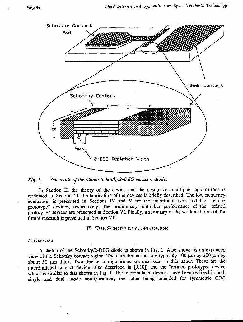
Fig. 1. Schematic of the planar Schottky/2-DEG varactor diode.
In Section II, the theory of the device and the design for multiplier applications isreviewed. In Section IE, the fabrication of the devices is briefly described. The low frequencyevaluation is presented in Sections IV and V for the interdigital-type and the "refinedprototype" devices, respectively. The preliminary multiplier performance of the "refinedprototype" devices are presented in Section VI. Finally, a summary of the work and outlook forfuture research is presented in Section VII.
II. THE SCHOTTKY/2-DEG DIODE
A. Overview
A sketch of the Schottky/2-DEG diode is shown in Fig. 1. Also shown is an expandedview of the Schottky contact region. The chip dimensions are typically 100 um by 200 [im byabout 50 |J.m thick. Two device configurations are discussed in this paper. These are theinterdigitated contact device (also described in [9,10]) and the "refined prototype" devicewhich is similar to that shown in Fig. 1. The interdigitated devices have been realized in bothsingle and dual anode configurations, the latter being intended for symmetric C(V)
Third International Symposium on Space Terahertz Technology Page 95
V a =0
V -Vva - vr
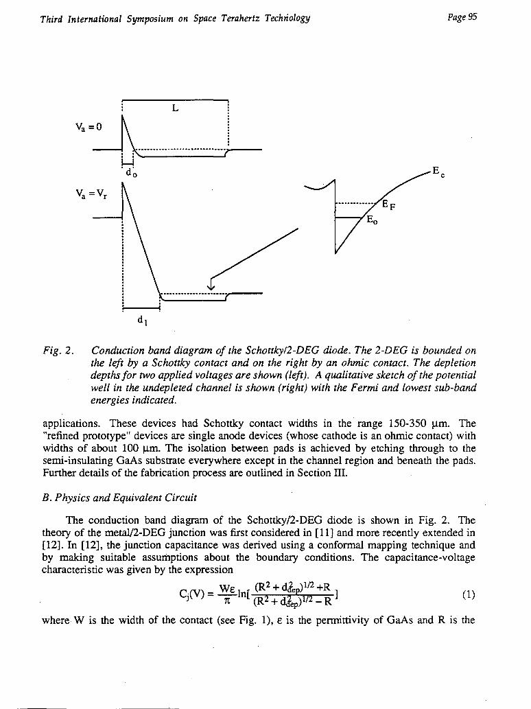
Fig. 2. Conduction band diagram of the Schottky/2-DEG diode. The 2-DEG is bounded onthe left by a Schottky contact and on the right by an ohmic contact. The depletiondepths for two applied voltages are shown (left). A qualitative sketch of the potentialwell in the undepleted channel is shown (right) with the Fermi and lowest sub-bandenergies indicated.
applications. These devices had Schottky contact widths in the range 150-350 Jim. The"refined prototype" devices are single anode devices (whose cathode is an ohmic contact) withwidths of about 100 |im. The isolation between pads is achieved by etching through to thesemi-insulating GaAs substrate everywhere except in the channel region and beneath the pads.Further details of the fabrication process are outlined in Section HI.
B. Physics and Equivalent Circuit
The conduction band diagram of the Schottky/2-DEG diode is shown in Fig. 2. Thetheory of the metal/2-DEG junction was first considered in [11] and more recently extended in[12]. In [12], the junction capacitance was derived using a conformal mapping technique andby making suitable assumptions about the boundary conditions. The capacitance-voltagecharacteristic was given by the expression
/ •p2_ i_H2 \lf2j--o(1)
where W is the width of the contact (see Fig. 1), e is the permittivity of GaAs and R is the
Page 96 Third International Symposium on Space Terahertz Technology
C.(V)
'sh
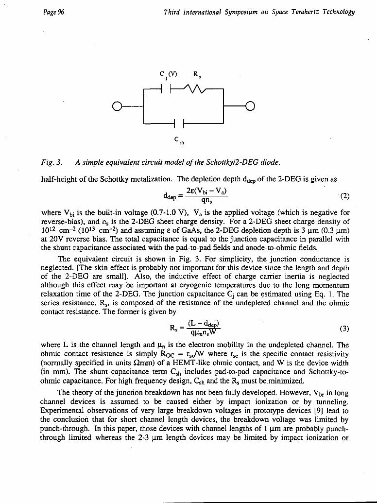
Fig. 3. A simple equivalent circuit model of the Schottky/2-DEG diode.
half-height of the Schottky metalization. The depletion depth2e(Vbi-Va)
, of the 2-DEG is given as
(2)
where Vbi is the built-in voltage (0.7-1.0 V), Va is the applied voltage (which is negative forreverse-bias), and ns is the 2-DEG sheet charge density. For a 2-DEG sheet charge density of1012 crrr2 (1013 crrr2) and assuming e of GaAs, the 2-DEG depletion depth is 3 (im (0.3 Jim)at 20V reverse bias. The total capacitance is equal to the junction capacitance in parallel withthe shunt capacitance associated with the pad-to-pad fields and anode-to-ohmic fields.
The equivalent circuit is shown in Fig. 3. For simplicity, the junction conductance isneglected. [The skin effect is probably not important for this device since the length and depthof the 2-DEG are small]. Also, the inductive effect of charge carrier inertia is neglectedalthough this effect may be important at cryogenic temperatures due to the long momentumrelaxation time of the 2-DEG. The junction capacitance Cj can be estimated using Eq. 1. Theseries resistance, Rs, is composed of the resistance of the undepleted channel and the ohmiccontact resistance. The former is given by
„ _ (L - ddep) (3)
where L is the channel length and m is the electron mobility in the undepleted channel. Theohmic contact resistance is simply ROC = rsc/W where r^ is the specific contact resistivity(normally specified in units Qmm) of a HEMT-like ohmic contact, and W is the device width(in mm). The shunt capacitance term Csh includes pad-to-pad capacitance and Schottky-to-ohmic capacitance. For high frequency design, CSh and the RS must be minimized.
The theory of the junction breakdown has not been fully developed. However, Vbr in longchannel devices is assumed to be caused either by impact ionization or by tunneling.Experimental observations of very large breakdown voltages in prototype devices [9] lead tothe conclusion that for short channel length devices, the breakdown voltage was limited bypunch-through. In this paper, those devices with channel lengths of 1 |im are probably punch-through limited whereas the 2-3 \un length devices may be limited by impact ionization or
Third International Symposium on Space Terahertz Technology Page 97
tunneling, or both. The breakdown voltage may also be limited by the geometry of the anodemetalization (for example, the half-height R) or by processing and material defects. A moredetailed discussion of the breakdown in these devices will be presented in a later paper.
C. Frequency and Power Limitations
Several factors limit the frequency response and power performance of the multiplier. Thefrequency response may be limited by the dynamic cutoff frequency which is usually defined[13] as
where Smax (Smin) is 1/Qnin (l/Qnax)> and Rs is the series resistance of the varactor diode. It isdesirable for the device to have a vco value much higher than the operating frequency to ensurethat the multiplier efficiency is not degraded. To achieve high vco, the series resistance shouldbe as small as possible, the minimum capacitance (near breakdown) should be small and thecapacitance modulation ratio Qnax/Qnin should be large.
Another important quantity which may limit both the frequency response and maximumoutput power is the finite velocity of the electrons traversing the modulation region (theepilayer in GaAs diodes or the 2-DEG channel in the Schottky/2-DEG diode). Recently,Kollberg et al [14] showed how the finite electron velocity limited the current in the 6P4 diodeused by Erickson [3]. Kollberg argued that the ac displacement current could not exceed thesaturation current which in turn is limited by the electron drift velocity. Using Monte Carloanalysis, the effective velocity and the saturation current in the 6P4 diode were estimated (in[14]) to be 2.4 x 107 cm/s and 44 mA, respectively. At input powers beyond that which causesthe current to saturate, the diode's rf impedance increases (since the current cannot). Kollbergused this analysis to simulate the roll-off in efficiency with input power, which was observedby Erickson.
The velocity saturation current is written here for the 2-d case as
Ivs = qnsveffW (5)
where ns is the 2-dimensional sheet charge density, W is the contact width and veff is theeffective velocity of the electrons in the channel. As will be shown, a Schottky/2-DEG diodewith W = 100 |im and ns = 1.85 x 10¹² cirr2 has roughly the same characteristics as the 6P4diode. Assuming the same effective velocity as was used for the 6P4, namely veff = 2.4 x 10⁷
cm/s, Ivs is about 70 mA.
The finite electron velocity may also limit the frequency response if the transit-time forelectrons traversing the modulation region is comparable to the period of the LO frequency,The transit-time corner frequency has been proposed [10] as a useful design parameter for thediode's frequency response, and is defined as
(6)
where L is the channel length (or the epilayer thickness in the standard diode). Note that the
Page 98 Third International Symposium on Space Terahertz Technology
frequency given by Eq. 6 is a corner frequency since, as the frequency increases beyond thisvalue, the maximum if modulation length shortens, resulting in a smaller capacitance ratio andthus to a roll-off in the multiplier efficiency. For example, assuming an effective electronvelocity of 2.4 x 107 cm/s (as was used in [14]), a varactor diode with input frequency of 80GHz will have a maximum modulation length of about 0.48 |0.m. In comparison, the 6P4 diode,which is often used at this frequency, has an epilayer thickness (and maximum dc modulationlength) of about 1.0 urn. Thus, both standard and 2-DEG diodes should be designed to achievea large capacitance modulation ratio within the length given by Eq. 6.
Having outlined the equations for the capacitance, resistance, punch-through voltage (Eq.2 with ddep = L), the dynamic cutoff and the transit-time frequencies and the saturation current,the Schottky/2-DEG diode may be designed for particular applications. This procedure issimplistic but is similar to the design of the state-of-the-art varactors currently in use. Thisdesign procedure was used for the "refined prototype" devices whose results are given inSection V. Before presenting the device results, the fabrication will be briefly reviewed.
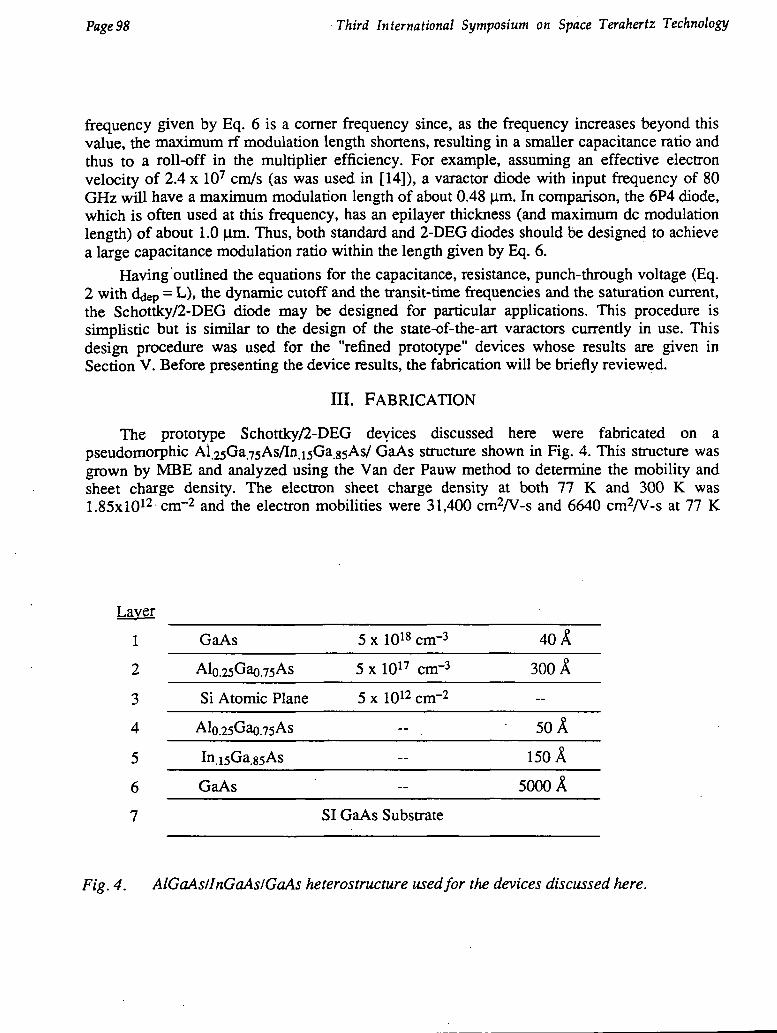
m. FABRICATION
The prototype Schottky/2-DEG devices discussed here were fabricated on apseudomorphic Al.2sGa.75As/In. isGa.gsAs/ GaAs structure shown in Fig. 4. This structure wasgrown by MBE and analyzed using the Van der Pauw method to determine the mobility andsheet charge density. The electron sheet charge density at both 77 K and 300 K was1.85xl012 crrr2 and the electron mobilities were 31,400 cm2/V-s and 6640 cm2/V-s at 77 K
Layer
1
2
3
4
5
6
7
GaAs
Alo.25Gao.7sAs
Si Atomic Plane
Alo.25Gao.7sAs
In.15Ga.85As
GaAs
5 x 1018 cm-3
5 x 1017 cm'3
5 x 1012 cm'2
—
—
—
SI GaAs Substrate
40 A
300 X
~
50A
150 A
5000 A
Fig. 4. AlGoAslInGaAslGaAs heterosiructure used for the devices discussed here.

Third International Symposium on Space Terahertz Technology Page 99
Fig. 5. Scanning electron micrographs of Schottky/2-DEG devices. The interdigitateddevice (top) has anode width of 250 Jim and channel length of 2 Jim. The "refinedprototype" device (bottom) shown here is similar to the devices discussed in SectionV. Here, the anode width is 100 M.IH and the channel length is 5 \im.

Page 100 Tnird International Symposium on Space Terahertz Technology
and 300 K, respectively. The supply and cap layers are substantially depleted to the 2-DEGand/or the surface, to minimize parallel conduction. The ohmic contact consists of anelectroplated SnNi/Ni/Au trilayer which is alloyed at about 380°C. To form the Schottkycontact, a trench is etched through the 2-DEG layer and a Pt/Au contact is electroplated intothe trench. Next, the contact pads are plated and finally a 2-3 micron deep NaOH:H2O2 etch tothe SI-GaAs substrate is performed to isolate the two pads. All lithography levels areperformed using a Karl Suss MJB-3 (405 nm). An SEM photo of the interdigitated device isshown in Fig. 5 (top). A sketch of a "refined prototype" is also shown (bottom). The roughsurface of this device was due to the isolation etch, performed using chlorine reactive ionetching. A subsequent wet chemical etch reduced the surface roughness considerably.
IV. Low FREQUENCY EVALUATION OF INTERDIGITATED DEVICESThe dc evaluation of the Schottky/2-DEG diodes include I(V), C(V) and reverse
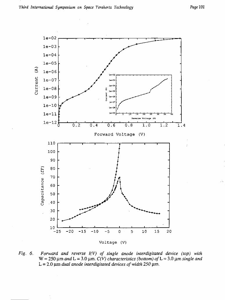
breakdown voltage measurements. First, the interdigitated device results are presented (theseresults were also presented in [10]). The forward and reverse I(V) of a single Schottky/2-DEGdevice is shown in Fig. 6 (top), measured at room temperature. The exponential diodecharacteristic is seen as the linear portion of this semi-log I(V) plot, in the range 0.35 - 0.7 V.The "knee" voltage (at 1 |iA) was 0.512V. The AV values for the current intervals 0.1 - l.OjiA,1.0 - lO.O^iA and 10.0 - 100(iA are 74mV, 74mV and 81mV, corresponding to inverse slopeparameters, V0, of 32.1mV, 32.1mV and 35.2mV, respectively. This corresponds to a diodeideality factor of 1.26. The series resistance of this device was determined to be 56Q. Theexpected 2-DEG channel resistance at room temperature is 6 Q. Allowing for a pessimisticvalue of the ohmic contact resistivity, r^ of 2.5 Qmm, the total series resistance expected forthis device was about 16 Q. The remaining 40 Q series resistance is most likely due toinsufficient plating of the ohmic contacts, as was substantiated by inspection using scanningelectron microscopy. The dual anode devices have no ohmic contact resistance. In thesedevices, the I(V) is dominated by the characteristic of the reverse-biased junction and a seriesresistance measurement cannot be made. However, using Eq. 3, the L = 2(im, W = 250^mdevice resistance is about 4 Q at 295K and about 1.0 Q at 100 K due to the increase in mobilityuponcooling.
The C(V) curves of the single and dual anode interdigitated devices are shown in Fig. 6(bottom). The channel length (gap between fingers) is 2 (im (3 p.m) for the dual (single)Schottky device. The anode widths were 250 jxm for both devices. As expected, the dualSchottky device has a nearly symmetric C(V) characteristic and it's zero-bias capacitance isabout half that of the single anode device. Subtracting the pad-to-pad capacitance which wasmeasured to be 4 fF, this symmetric C(V) device had a dynamic cutoff frequency of about 1THz at 295K and about 4 THz at 100 K. The velocity saturation current (Eq. 5 usingveff = 2.4 x 107 cm/s) is 178 mA. Also, the transit-time corner frequency of the 2 Jim channellength device is about 19 GHz, calculated using Eq. 6. The capacitance levels of the dualanode device is probably too high for most multiplier applications. Nevertheless, multipliertesting of these devices will be performed in the near future.
Third International Symposium on Space Terahertz Technology Page 101
•M
0)OGtO4J•HO
o
110
100
90
80
70
60
50
40
30
20
10-25
0 .2 0.4 0 .6 0 .8 1 .0
Forward Voltage (V)
1.2 1.4
-20 -15 -10 -5 10 15 20
Voltage (V)
Fig. 6. Forward and reverse I(V) of single anode interdigitated device (top) withW = 250 (im and L = 3.0 |im. C(V) characteristics (bottom) ofL = 3.0 (im single andL = 2.0 |im dual anode interdigitated devices of width 250

Page W2 Third International Symposium on Space Terahertz Technology
U-i
1)OC(04->-Hum
o
40
35
30
25
20
15
10
DataFit
10 12 14
Reverse Voltage (V)
C(V) of refined prototype device A. Also shown is a fit (Eq. 1) using R = 0.75 fim,CSh = 8.0 fF, Vbi = 0.7 V andW = 90
Fig. 7.
V. Low FREQUENCY EVALUATION OF REFINED PROTOTYPE DEVICESThe refined prototype devices had two anode width/channel length combinations. The
"A" devices had anode widths of 90 (im (on average) and channel lengths of 2.5 |im while the"B" devices had anode widths of 80 ^im and channel lengths of 3.0 |im. The C(V) characteristicof device A is shown in Fig. 7. The theoretical capacitance, shown fitted to the data, agreeswell with the data except near zero-bias where the fit is lower than the data. The fit assumed areasonable value of the anode metal half-height (R = 0.75 Jim) and a shunt capacitance of 8.0fF. This value of CSh is higher than expected since the pad-to-pad capacitance was measured tobe about 2 fF. The additional shunt capacitance may be due in part to fields between the anodeand ohmic metals. This contribution to the capacitance is not easily determined and is also notsubstracted for the vco calculations. The difference between the theory and the data near zero-bias is either due to inaccuracy of Eq. 1 for the geometry of this device or to effects related tothe leakage current at low bias. We are currently investigating a more general theory of thejunction capacitance for devices of various geometries.
The forward I(V) as a function of temperature of device A is shown in Fig. 8. As thetemperature decreased, several changes occured. First, the entire I(V) curve shifted to highervoltages, as expected due to the temperature dependence of the saturation current (the theory ofthe thermionic saturation current of the Schottky/2-DEG junction is being investigated [15]).At lower currents, the "leakage" current which has been routinely observed at roomtemperature is seen to decrease substantially so that, at 220 K, it is much less than onenanoamp. Finally, the strong temperature dependence of the series resistance is evident at highcurrents.

Third International Symposium on Space Terahertz Technology Page 103
5
le-01
le-02
le-03
le-04
le-05
le-06
le-07
le-08
le-09
le-100
CO
,CO
Oc
CO•HCO0)
30
25
20
15
10
5
0.2 0.4 0.6 0.8
Forward Voltage (V)
23 K40 K60 K80 K100 K120 K140 K160 K180 K200 K220 K240 K260 K280 K299 K
1.0 1 .2
0 50 250 300100 150 200
Temperature (K)
Fig. 8. Forward I(V) (top) and series resistance (bottom) versus temperature of device A.
Page 104 Third International Symposium on Space Terahertz Technology
le-04
le-05
S le-06
O
M0)
le-07
le-08
le-09
40 K —60 K —80 K -J
100 K —120 K140 K168 K190 K200 K220 K240 K —260 K295 K J
0 2 4 6 8 10 12
Reverse Voltage (V)
Fig. 9. Reverse I(V) versus temperature of device A.
14 16 18
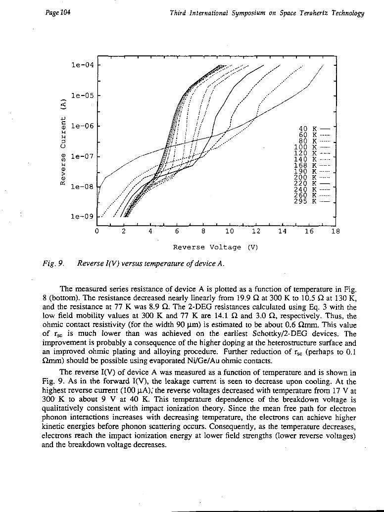
The measured series resistance of device A is plotted as a function of temperature in Fig.8 (bottom). The resistance decreased nearly linearly from 19.9 Q at 300 K to 10.5 Q at 130 K,and the resistance at 77 K was 8.9 Q. The 2-DEG resistances calculated using Eq. 3 with thelow field mobility values at 300 K and 77 K are 14.1 Q and 3.0 Q, respectively. Thus, theohmic contact resistivity (for the width 90 |0.m) is estimated to be about 0.6 Qmm. This valueof r^ is much lower than was achieved on the earliest Schottky/2-DEG devices. Theimprovement is probably a consequence of the higher doping at the heterostructure surface andan improved ohmic plating and alloying procedure. Further reduction of rsc (perhaps to 0.1Qmm) should be possible using evaporated Ni/Ge/Au ohmic contacts.
The reverse I(V) of device A was measured as a function of temperature and is shown inFig. 9. As in the forward I(V), the leakage current is seen to decrease upon cooling. At thehighest reverse current (100 (j.A),"the reverse voltages decreased with temperature from 17 V at300 K to about 9 V at 40 K. This temperature dependence of the breakdown voltage isqualitatively consistent with impact ionization theory. Since the mean free path for electronphonon interactions increases with decreasing temperature, the electrons can achieve higherkinetic energies before phonon scattering occurs. Consequently, as the temperature decreases,electrons reach the impact ionization energy at lower field strengths (lower reverse voltages)and the breakdown voltage decreases.
Third International Symposium on Space Terahertz Technology Page 105
le-02
le-03
le-04*̂ *«
5~ le-05c2 le-06
le-07
le-08
le-09
5
<
cQ)
U
le-04
le-05
le-06
le-07
le-08
"22K"5 OK
"100Ki- "142K1
"200K 1
"263K1
"299K 1
////III
299 K -•2 6 0 K - ~220 K-180 K -140 K -100 K -.
60 K -24 K -
0 0.2 0.4 0.6 0.8 1.0 1.2 1.4
Forward Voltage (V)
10 15 20
Reverse Voltage (V)
25 30
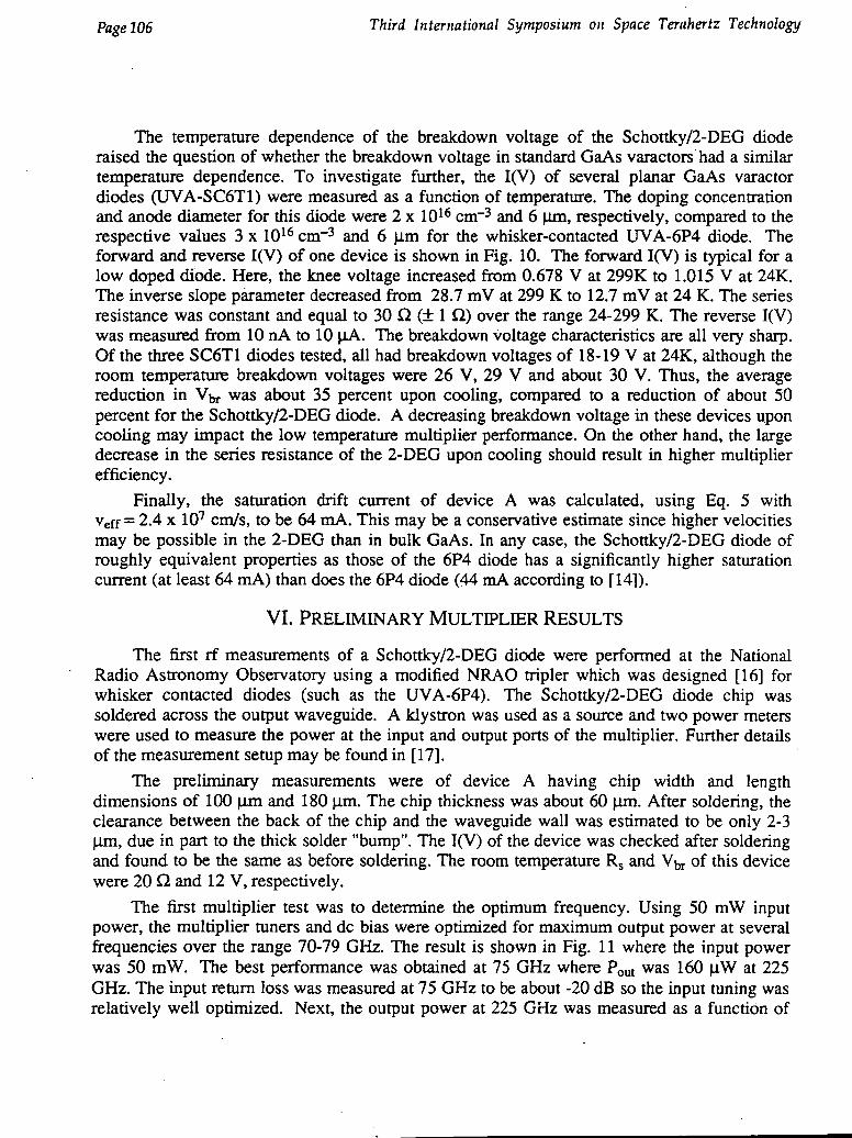
Fig. 10. Forward I(V) (top) and reverse I(V) (bottom) vs. temperature of planar GaAsSchottky diode SC6T1.
Page 106 Third International Symposium on Space Terahertz Technology
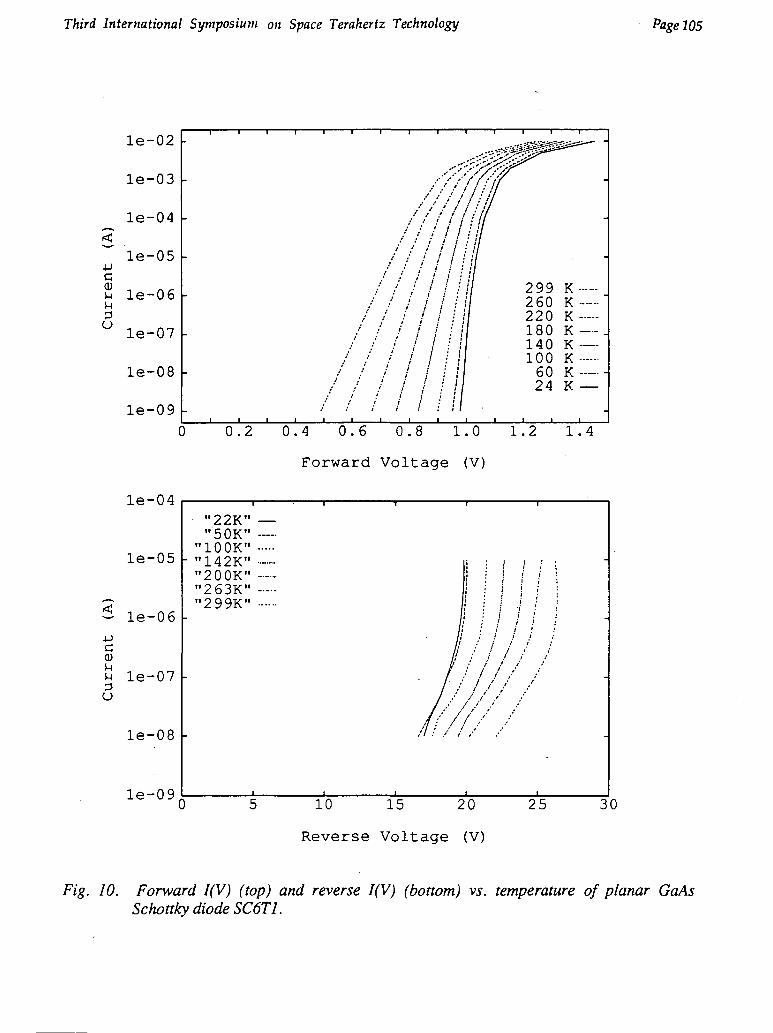
The temperature dependence of the breakdown voltage of the Schottky/2-DEG dioderaised the question of whether the breakdown voltage in standard GaAs varactors had a similartemperature dependence. To investigate further, the I(V) of several planar GaAs varactordiodes (UVA-SC6T1) were measured as a function of temperature. The doping concentrationand anode diameter for this diode were 2 x 1016 cm~3 and 6 urn, respectively, compared to therespective values 3 x 1016 cm~3 and 6 Jim for the whisker-contacted UVA-6P4 diode. Theforward and reverse I(V) of one device is shown in Fig. 10. The forward I(V) is typical for alow doped diode. Here, the knee voltage increased from 0.678 V at 299K to 1.015 V at 24K.The inverse slope parameter decreased from 28.7 mV at 299 K to 12.7 mV at 24 K. The seriesresistance was constant and equal to 30 Q (± 1 Q) over the range 24-299 K. The reverse I(V)was measured from 10 nA to 10 ^lA. The breakdown voltage characteristics are all very sharp.Of the three SC6T1 diodes tested, all had breakdown voltages of 18-19 V at 24K, although theroom temperature breakdown voltages were 26 V, 29 V and about 30 V. Thus, the averagereduction in Vbr was about 35 percent upon cooling, compared to a reduction of about 50percent for the Schottky/2-DEG diode. A decreasing breakdown voltage in these devices uponcooling may impact the low temperature multiplier performance. On the other hand, the largedecrease in the series resistance of the 2-DEG upon cooling should result in higher multiplierefficiency.
Finally, the saturation drift current of device A was calculated, using Eq. 5 withveff = 2.4 x 107 cm/s, to be 64 mA. This may be a conservative estimate since higher velocitiesmay be possible in the 2-DEG than in bulk GaAs. In any case, the Schottky/2-DEG diode ofroughly equivalent properties as those of the 6P4 diode has a significantly higher saturationcurrent (at least 64 mA) than does the 6P4 diode (44 mA according to [14]).
VI. PRELIMINARY MULTIPLIER RESULTSThe first rf measurements of a Schottky/2-DEG diode were performed at the National
Radio Astronomy Observatory using a modified NRAO tripler which was designed [16] forwhisker contacted diodes (such as the UVA-6P4). The Schottky/2-DEG diode chip wassoldered across the output waveguide. A klystron was used as a source and two power meterswere used to measure the power at the input and output ports of the multiplier. Further detailsof the measurement setup may be found in [17].
The preliminary measurements were of device A having chip width and lengthdimensions of 100 (im and 180 |im. The chip thickness was about 60 fim. After soldering, theclearance between the back of the chip and the waveguide wall was estimated to be only 2-3Jim, due in part to the thick solder "bump". The I(V) of the device was checked after solderingand found to be the same as before soldering. The room temperature Rs and Vbr of this devicewere 20 Q and 12V, respectively.
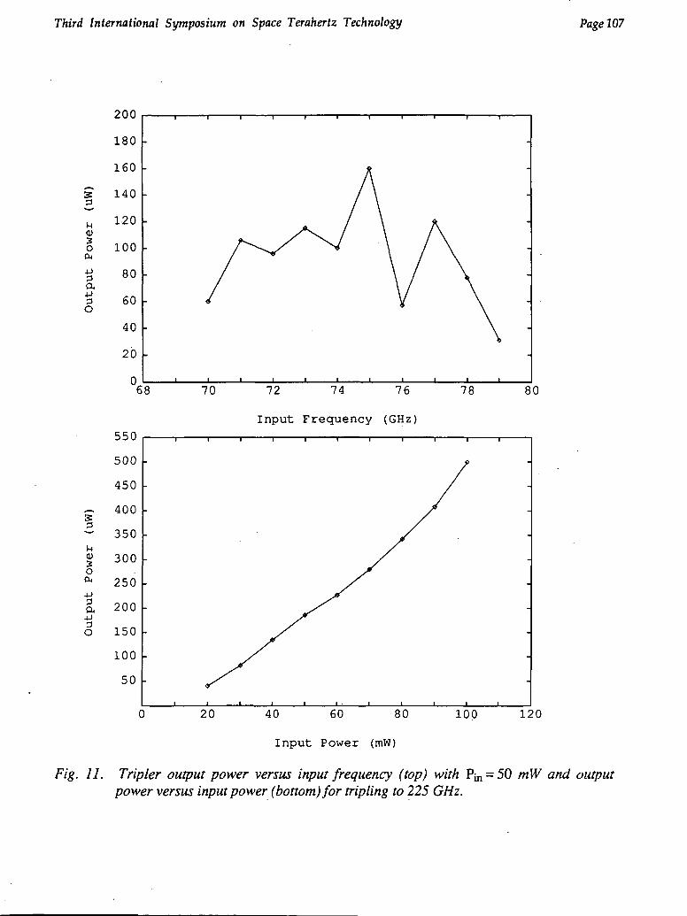
The first multiplier test was to determine the optimum frequency. Using 50 mW inputpower, the multiplier tuners and dc bias were optimized for maximum output power at severalfrequencies over the range 70-79 GHz. The result is shown in Fig. 11 where the input powerwas 50 mW. The best performance was obtained at 75 GHz where Pout was 160 p.W at 225GHz. The input return loss was measured at 75 GHz to be about -20 dB so the input tuning wasrelatively well optimized. Next, the output power at 225 GHz was measured as a function of
Third International Symposium on Space Terahertz Technology Page W7
MOJ
OCM
-P3a
4->3O
33
Ma;
-3o
200
180
160
140
120
100
80
60
40
20
0(
550
500
450
400
350
300
250
200
150
100
50
68 70 72 74 76
Input Frequency (GHz)
78 80
0 20 40 60 80
Input Power (mW)
100 120
Fig. 11. Tripler output power versus input frequency (top) with Pin = 50 mW and outputpower versus input power (bottom) for tripling to 225 GHz.
PageT.08 Third International Symposium on Space Terahertz Technology
the input power, as shown in Fig. 11 (bottom). P-m was varied over the range 20 -100 mW. Asthe input power increased, the output power increased, reaching a maximum value of 500 |iWat 100 mW at the input. This corresponds to an efficiency of 0.5 percent. In comparison,Bradley [17] used this multiplier with a planar GaAs varactor of doping 1.1 x 1017 cm~3 anddiameter 7 |im and obtained 3.7 mW output power and 4.1 percent efficiency at 219 GHz. Thisfirst multiplier measurement of the Schottky/2-DEG diode is encouraging but much higherperformance should be possible. Even the current devices should yield higher multiplierefficiencies if they are thinned to 25 [im or less and if a thinner solder layer is used to reducethe shunt capacitance between the chip and the waveguide wall.
vn. SUMMARY AND FUTURE RESEARCH
In summary, we have reported on the recent progress in the research of a novelSchottky/2-DEG varactor diode. Observations of reduced breakdown voltages upon cooling inboth the standard GaAs and the novel Schottky/2-DEG diodes were in agreement with thetheory of impact ionization. The problem of current saturation was discussed and theSchottky/2-DEG diode of width 90 |im was found to have a significantly higher saturationcurrent than the comparable GaAs 6P4 varactor. Recent improvements to the design andfabrication procedures have resulted in devices having lower series resistance and lowercapacitance. Both single anode and dual anode (with symmetric C(V)) devices have beeninvestigated. The cutoff frequency of the dual anode device was estimated to be 1 THz (4 THz)at 300 K (100 K), whereas the single anode device had cutoff frequency of about 0.6-1.0 THz,depending on the temperature. Preliminary multiplier measurements of a single anode devicewere encouraging, resulting in 500 ^.W output power at 225 GHz with 0.5 percent efficiency.Ongoing research will include more extensive multiplier testing of both the single anode andthe symmetric C(V) devices. Also, shorter channel length devices with Ni/Ge/Au ohmiccontacts will be fabricated to achieve much higher cutoff and transit-time frequencies. Inaddition, AlInAs/InGaAs/InP heterostructures will be investigated. Finally, the theoriesrelating to the junction capacitance and breakdown are being developed and the currenttransport in these devices will be investigated using Monte Carlo simulations.
ACKNOWLEDGEMENTSThis work has been supported by the National Science Foundation under contracts ECS-
8720850 and ECS-9113123 (contract monitors Dr. T. Hsiang and Dr. B. Clifton) and by. theOffice of Naval Research under contract #N00014-90-J-4006 (contract monitor Dr. Y.S. Park).The authors thank R. Bradley and N. Horner of the National Radio Astronomy Observatory forassistance with the multiplier measurements, and T. Hierl of Quantum Epitaxial Designs, Inc.for providing the MBE material and Van der Pauw data.
Third International Symposium on Space Terahertz Technology Page 109
REFERENCES[I] H. P. Ro'ser, "Heterodyne Spectroscopy for Submillimeter and Far-Infrared Wavelengths From 100
urn to 500 |xm," Infrared Physics, Vol. 32, pp. 385-407,1991.
[2] J. Zmuidzinas, A.L. Betz, and R.T. Boreiko, "A Corner-Reflector Mixer Mount for Far InfraredWavelengths," Infrared Phys., Vol. 29, No. 1,119-131,1989.
[3] N. Erickson, "High Efficiency Submillimeter Frequency Multipliers," The 1990 IEEE MTT-S Int.Microwave Symposium, Dallas, TX, May 1990.
[4] P. Zimmermann, private communication, March and May 1990.
[5] T. W. Crowe, W.C.B. Peatman, and E. Winkler, "GaAs Schottky Barrier Varactor Diodes forSubmillimeter Wavelength Power Generation," Microwave and Optical Tech. Lett., Special Issue:Space Terahertz Tech., Vol. 3, No. 1, January 1991.
[6] K. Benson and M.A. Frerking, "Theoretical Efficiency for Triplers Using Nonideal Varistor Diodesat Submillimeter Wavelengths," IEEE Trans. Microwave Theory Tech., Vol. MTT-33, No. 12,1367-1374, Dec. 1985.
[7] C. Kidner, I. Medhi, J. East, G. Haddad, "Performance Limitations of Resonant Tunneling Diodes,"The First Int'l. Symposium on Space Terahertz Technology, Ann Arbor, MI, March 1990.
[8] H. Rothermel, T.G. Phillips, J. Keene, "A Solid-State Frequency Source for Radio Astronomy inthe 100 to 1000 GHz Range," Int. J. Infrared and Millimeter Waves, Vol. 10, No. 1, 83-100, 1989.
[9] W. C. B. Peatman, T. W. Crowe and M. Shur, "Design and Fabrication of Heterostructure VaractorDiodes for Millimeter and Submillimeter Wave Multiplier Applications," Proc. IEEE/CornellConf. on Advanced Concepts in High Speed Semic. Dev. and Circuits, Ithaca, NY, 1991.
[10] W.C.B. Peatman, T.W. Crowe and M. .Shur, "A Novel Schottky/2-DEG Diode for Millimeter andSubmillimeter Wave Multiplier Applications," IEEE Electron Device Lett., Vol. 13, No. 1, pp. 11-13, January 1992.
[II] S.G. Petrosyan and A. Ya Shik, "Contact Phenomena in a two-dimensional electron gas," SovietPhysics Semicond., 23 (6), pp. 696-697, June 1989.
[12] B. Gelmont, M. Shur and C. Moglestue, "Theory of Junction Between Two-Dimensional ElectronGas and P-Type Semiconductor," to be published, IEEE Trans. Electron Devices, Vol. 39, No. 5,May 1992.
[13] P. Penfield and R. Rafuse, Varactor Applications, MIT Press, 1962, p. 86.
[14] E. Kollberg, T. Tolmunen, M. Frerking and J. East, "Current Saturation in Submillimeter WaveVaractors," Proc. Second Int'l. Symp. Space Terahertz Technology, Pasadena, CA, pp. 307-322,1991.
[15] B. Gelmont, M. Shur (unpublished).
[16] J. Archer, "An Efficient 200-290 GHz Frequency Tripler Incorporating A Novel StriplineStructure," IEEE Trans. Micrwave Theory and Tech., Vol. 32, No.' 4, pp. 416-420,1984.
[17] R. Bradley, Ph.D. Thesis, University of Virginia, pp. 42-65 May, 1992.