development of a statistical model for npn bipolar ... · development of a statistical model for...
TRANSCRIPT
Development of a Statistical Model
for NPN Bipolar Transistor Mismatch by
Maurice J. Lamontagne
A Project Report
Submitted to the Faculty
of
WORCESTER POLYTECHNIC INSTITUTE
In partial fulfillment of the requirements for the
Degree of Master of Science
in
Industrial Mathematics
May 2007
APPROVED: ______________________________________________ Jayson D. Wilbur, Advisor ______________________________________________ Bogdan M. Vernescu, Department Head

Abstract Due to the high variation of critical device parameters inherent in integrated circuit manufacturing, modern integrated circuit designs have evolved to rely on the ratios of similar devices for their performance rather than on the absolute characteristics of any individual device. Today's high performance analog integrated circuits depend on the ability to make identical or matched devices. Circuits are designed using a tolerance based on the overall matching characteristics of their particular manufacturing process. Circuit designers also follow a general rule of thumb that larger devices offer better matching characteristics. This results in circuits that are over designed and circuit layouts that are generally larger than necessary. In this project we develop a model to predict the mismatch in a pair of NPN bipolar transistors. Precise prediction of device mismatch will result in more efficient circuit deigns, smaller circuit layouts and higher test yields, all of which lead to into more reliable and less expensive products.
ii

Acknowledgements I would like to thank my project advisor, Professor Jayson Wilbur. Without his guidance and insightfulness this paper would not have been possible. And Professor Suzanne Weekes for keeping me on track during my course of study. I would also like to thank Ted Neira for his advice into the practical matters of what we were trying to accomplish with this paper. Most of all, I would like to thank my wife Kathryn and the rest of my family for their unwavering support and encouragement during my studies at WPI. It has been a long road.
iii

Table of Contents List of Figures ……………………………………………………………..………. v List of Tables ….………………………………………………………………...… vi 1. Introduction …………………………………………………………………..…. 1 1.1. Motivating problem ……………………………………………………..…. 1 1.2. Literature Review ……………………………………………………...…. 5 1.3. Physical model ………………………………………………….……..…. 6 1.4. Plan ………………………………………………………………..…..…. 7 2. Experiment design ………………………………………………………....…. 9 3. Pilot study ……………………………………………………………….....…. 13 3.1. Experimental design ……………………………………………….…..…. 13 3.2. Preliminary statistical model …………………………………………..…. 14 3.3. Simplified model ……………………………………………………....…. 18 3.4. Results of the pilot study ……………………………………………...…. 20 3.5. Sample size calculation for final run …………………………...……..…. 20 4. Final run ……………………………………………………………..……..…. 22 4.1. Design of the final run ………………………………………………...…. 22 4.2. Analysis and final results ………………………..…………………………. 23 4.3. Look-up table …………………………………………………………....…. 27 5. Conclusions …………………………………………………………………..…. 28 6. References …………………………………………………………..………..…. 29 Appendices ……………………………………………………………….……..…. 30 A.1. SAS code for the analysis of the pilot study ………………………..…..…. 30 A.2. SAS code for the determination of the sample size for the final run .…..…. 32 A.3. SAS code for the analysis of the final run ……………………………...…. 35
iv

List of Figures Figure 1.1. Schematic of a common emitter amplifier ………………………....…. 2 Figure 1.2. Pot of common emitter amplifier output voltage …………………..…. 2 Figure 1.3. Schematic of a differential amplifier ……………………………….…. 3 Figure 1.4. Pot of differential amplifier output voltage …………………….…..…. 4 Figure 1.5. An example plot of transistor current vs. base-emitter voltage ….....…. 7 Figure 2.1. Drawing of a matched pair of transistors ………………………......…. 9 Figure 2.2. Drawing of the experimental unit or test die …………………….……. 10 Figure 2.3. Photograph of an experimental wafer ……………………………....…. 11 Figure 2.4. Schematic of test setup ………………………………………...…...…. 11 Figure 2.5. Example of the test output ……………………………………….....…. 12 Figure 3.1. Test order of the experimental units for the pilot study .…………...…. 13 Figure 3.2. Normal quantile plot of the residuals of the preliminary model …...…. 16 Figure 3.3. Normal quantile plot of the residuals of the simplified model ...…...…. 19 Figure 3.4. Plot of the Margin of error of the simplified model vs. sample size .…. 21 Figure 4.1. Test order of the replicates for the final run …………………….….…. 22 Figure 4.2. Normal quantile plot of the residuals of the final model ….……...…. 24 Figure 4.3. Location of outliers ………………………………………………....…. 25 Figure 4.4. Normal quantile plot of the residuals of the final
model with the outliers removed ………………………………………. 26
v

List of Tables Table 2.1. List of the devices used in the experiment …………………...……...…. 10 Table 2.2. Test conditions for the experiment ………………………………….…. 12 Table 3.1. Test order of the devices in each replicate for the pilot study ….…...…. 14 Table 3.2. Results of the analysis of the preliminary model …………………....…. 15 Table 3.3. Results of the analysis of the simplified model ……………………..…. 19 Table 4.1. Final run test order ……………………………………………...…...…. 23 Table 4.2. Final run outliers ………………………………………………….....…. 24 Table 4.3. Final Model Results ………………………………………………....…. 25 Table 4.4. Look-up table ………………………………………………………..…. 27
vi

1. Introduction 1.1. Motivating Problem
The integrated circuit manufacturing industry is built on economies of scale. The
ability to make millions of virtually identical circuit “chips” offset the high development
costs associated with new circuit designs. However, the manufacturing process itself has
poor absolute tolerances. Key electrical parameters, such as bipolar transistor gain can
vary by many percentage points within a manufacturing lot and variations as high as 20
percent from one lot to the next is not uncommon.
It has been shown that the variation of device characteristics for adjacent
components is much smaller than the overall variation in the manufacturing process.
Therefore circuit designs have evolved that rely on the ratio of adjacent devices rather
than on the absolute value of any one component. This strategy has made modern circuits
more complex than those of the past but counter-intuitively, it has also made them easier
to manufacture and more reliable.
This point is illustrated by way of an example. The Common-Emitter (CE)
amplifier shown in Figure 1.1 is a circuit that is widely used due to its simplicity. The
circuit consists of a single transistor, Q1, and two resistors. Its main drawback is that the
output voltage (VOUT) is very sensitive to the gain of the transistor Q1. The gain of Q1,
known as BF, is itself sensitive to changes in the manufacturing process. In fact, BF can
change as much as 40 percent (some nominal value ±20%) over the time that a product
is being made.
1

Figure 1.1 Common-Emitter amplifier circuit schematic
Figure 1.2 Common-Emitter amplifier output voltage
for different levels of BF
2

This sensitivity of C-E amplifier performance to the manufacturing process has
relegated the C-E amplifier to non-critical applications that can handle the wide range of
output voltages. Contrast this design to that of the differential amplifier shown in Figure
1.3. The differential amplifier circuit, or diff-amp, forms the heart of every modern
integrated circuit amplifier design.
Figure 1.3 Differential amplifier circuit schematic
As is seen in Figure 1.3, the diff-amp is much more complicated than the C-E
amplifier, using six transistors instead of just one. It should also be noted that with the
exception of resistor R0, all the circuit components are used in pairs. QP1 is paired with
QP2, QN1 with QN2, and so on. This pairing, or matching of devices, is what makes the
diff-amp robust. Figure 1.4 shows the output voltage of the diff-amp under the same
3

operating conditions as the C-E amplifier of Figure 1.1. It can be seen that the output
voltage of the diff-amp hardly changed at all as BF changed ±20% whereas the output
voltage of the C-E amplifier changed in direct proportion to the change in BF.
Figure 1.4 Differential amplifier output voltage
for different levels of BF
Circuits like the diff-amp rely on the fact that alike components placed adjacent to
one another can be expected to have nearly identical electrical characteristics. The
magnitude of their difference is called device mismatch. The amount of device mismatch
is critical to analog circuit design. Without an accurate estimate of device mismatch,
circuit designers tend to “over design” a circuit so it will be guaranteed to work. This
could mean adding circuit blocks that compensate for a voltage swing as shown in Figure
1.2. This, of course increases the complexity of the circuits, which makes them more
4

difficult to manufacture, affecting manufacturing and test yields, which ultimately drives
up their cost.
It is generally assumed that device mismatch is constant over the operating range
of the devices, although this is rarely quantified. It is also generally assumed that the
magnitude of device mismatch varies inversely with the active area of the devices.
Therefore, in parts of the circuit where device matching is crucial, designers will
typically use the largest device available. This increases the overall physical size of the
circuit again driving up the manufacturing cost.
The primary goal of this project was to determine what affect the transistor active
area and operating conditions have on device mismatch. A lookup table will be compiled
showing the correct size of transistor to use for a user-defined level of device mismatch.
1.2. Literature Review
Drennan et al. (1998) and Ngo et al. (1990) both present deterministic mismatch
models based on device geometry and process parameters. Drennan presents a single,
complete NPN mismatch model to account for all the variation in mismatch, whereas the
Ngo model decomposes the NPN device into a circuit composed of an ideal transistor in
conjunction with various unintended or parasitic devices. Mismatch is then modeled as
the variation in the parasitic devices. Extraction of the parameters for both models
depends on detailed knowledge of bipolar device construction and the manufacturing
process, information that is not always available to the users of a particular process. As
designed, the Drennan model only fits vertical devices. Lateral devices such as PNP
transistors, for which matching is generally less critical would require a separate model.
5
Similarly the Ngo method would require the identification of the parasitic components of
each new device type to be modeled. The model presented here is based on the statistics
of the transistors’ output characteristics and could easily be extended to devices of any
type.
Pergoot et al. (1995) outline a statistical method for analyzing mismatch data.
They present tests for means and normality and ultimately show how to calculate the
sample size needed to guarantee a given confidence level. Holer (2000) goes a different
route, proposing to use Monte Carlo simulations to describe the mismatch in devices
caused by random process variation. In this project we consider the problem of device
selection based on a statistical model for mismatch.
1.3. Physical model
An important test in determining the operating characteristics of a bipolar
transistor is the Gummel test. In the Gummel test, the collector and base currents (IC and
IB) are measured while the base-emitter voltage (VBE) is swept and the collector-emitter
voltage (VCE) is held constant. An example of a Gummel plot is shown in Figure 1.5.
At low base-emitter voltages the collector current can be modeled by the
following equation:
NFVV
SCT
BE
eII =
Where IS is the saturation current and is directly proportional to the active area of the
device, VBE is one of the test conditions and is varied from a low value to a high value,
VT is the thermal voltage and is very sensitive to temperature but unaffected by the
electrical test conditions and NF is called the emission coefficient is usually set equal to 1.
6

Figure 1.5 An example of a Gummel plot
At higher values of VBE the curve deviates from this log-linear behavior due to
internal resistances and a phenomenon known as current crowding. As most circuit
designers avoid this area when device matching is critical, it was decided to limit the
experiment to the log-linear region of operation.
1.4. Plan
The primary goal of this project was to determine what affect the transistor active
area and operating conditions have on device mismatch. Pairs of NPN Bipolar Junction
Transistors (BJT) of various sizes were measured under different operating conditions.
These data will be used to develop a model to predict the amount of mismatch for pairs of
transistors of varying size and test conditions. Finally, a lookup table will be compiled
listing the best transistor size to use for a given level of mismatch and operating
condition. The idea is to develop a tool for circuit designers that is easy to use and
7

implement. All data were collected using the Gummel test described above. Input from
circuit designers was used to determine the range of operating conditions.
The experimental unit in this experiment was a test structure that contained three
matched pairs of NPN BJTs with each transistor pair having a different active area. This
test structure was replicated numerous times on experimental wafers.
Since it was unknown at the start of this project what the final model would be a
pilot study was run first. Due to test time constraints, the sample size for the pilot study
was limited to all available test structures on one experimental wafer. The sample size
was evaluated at the end of the pilot study to make sure it was adequate and a new sample
size was determined for the final run of the experiment. Analysis of the pilot study data
was used to refine the test procedure and statistical model for the final run of the
experiment.
8
2. Design of the Experiment
Due to the discrete nature of the levels, it was decided to use a randomized
complete block design (RCBD) for this experiment. An effects model was developed to
fit the data and analyzed using analysis of variance (ANOVA) techniques. The
experimental factors looked at are AREA and VBE. Due to test time constraints it was
not possible to randomize the testing of the replicates in the pilot study, so REPLICATE
number was added as a factor in the model. After the pilot study was conducted and
analyzed, the experimental setup and model were refined and the final run of the
experiment was conducted and analyzed.
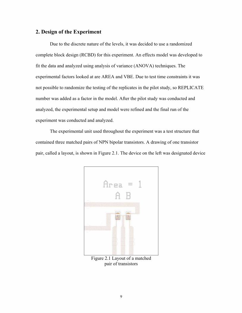
The experimental unit used throughout the experiment was a test structure that
contained three matched pairs of NPN bipolar transistors. A drawing of one transistor
pair, called a layout, is shown in Figure 2.1. The device on the left was designated device
Figure 2.1 Layout of a matched
pair of transistors
9
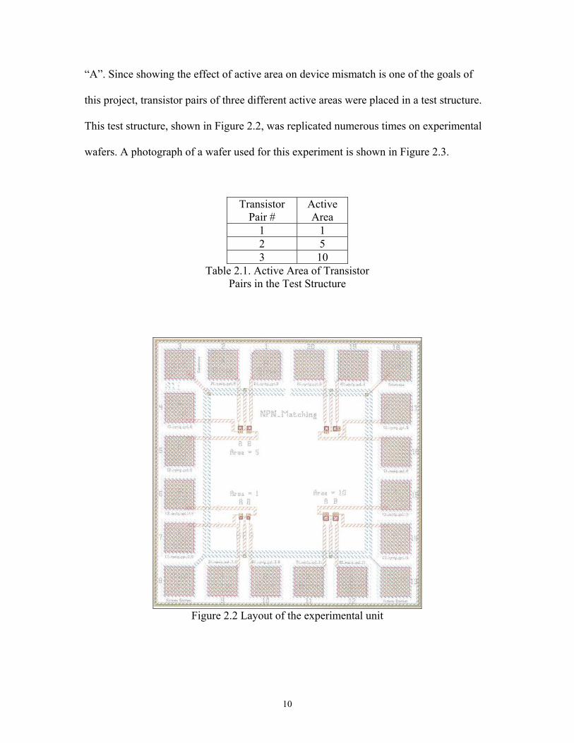
“A”. Since showing the effect of active area on device mismatch is one of the goals of
this project, transistor pairs of three different active areas were placed in a test structure.
This test structure, shown in Figure 2.2, was replicated numerous times on experimental
wafers. A photograph of a wafer used for this experiment is shown in Figure 2.3.
Transistor Pair #
Active Area
1 1 2 5 3 10
Table 2.1. Active Area of Transistor Pairs in the Test Structure
Figure 2.2 Layout of the experimental unit
10

Figure 2.3 Photograph of an Experimental Wafer
The test system consisted of an HP4156 Semiconductor Parameter Analyzer
connected to a probe station through a Keithley 707A switching matrix. The test system
was run by Silvaco Utmost III software, which controlled the test equipment and
recorded the measurements. The schematic of the test setup is shown in Figure 2.4. The
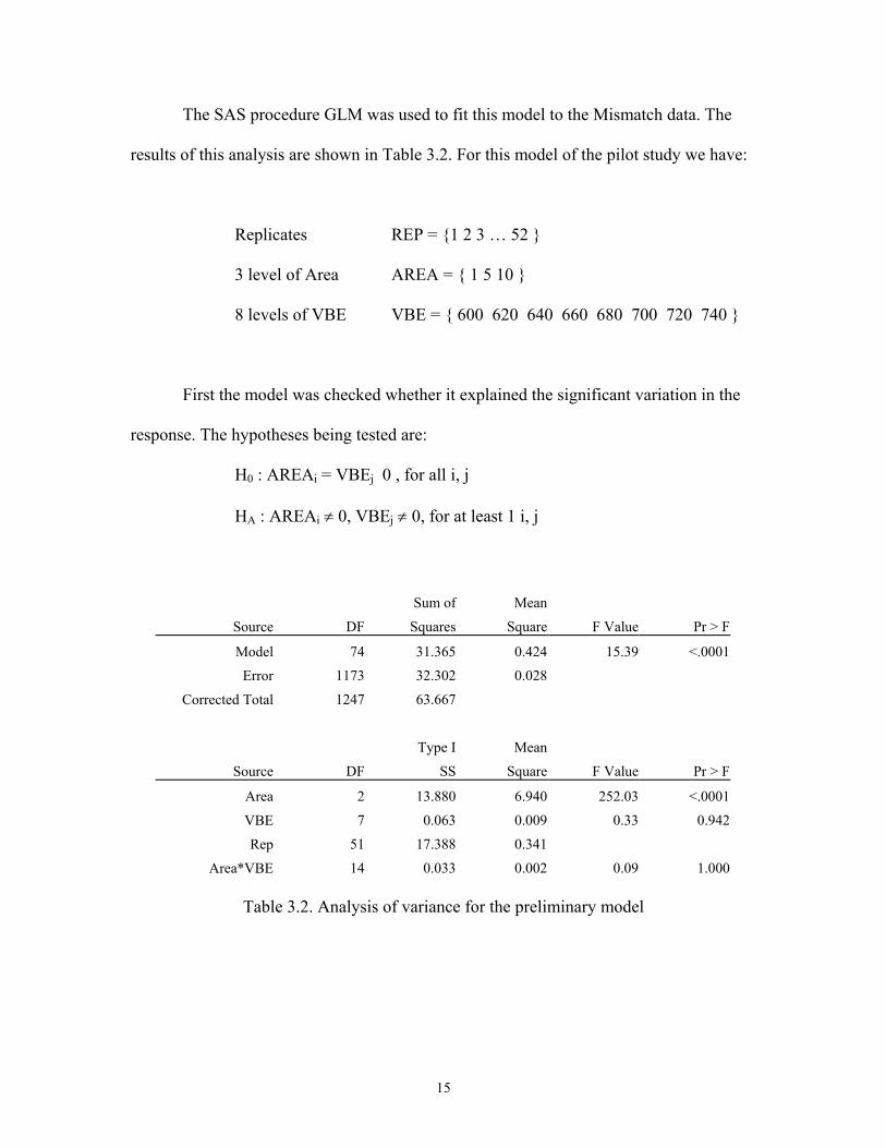
electrical test points are listed in Table 2.2. During testing, the collector-emitter voltage,
VCE, was held constant while the base-emitter voltage, VBE, was swept from the low
value to the high value while the collector current was measured. An example of the test
output is shown in Figure 2.5. This setup was kept constant throughout the experiment.
11
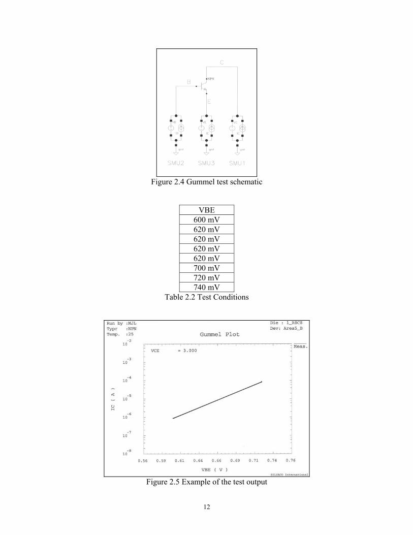
Figure 2.4 Gummel test schematic
VBE 600 mV 620 mV 620 mV 620 mV 620 mV 700 mV 720 mV 740 mV
Table 2.2 Test Conditions
Figure 2.5 Example of the test output
12

3. Pilot Study
3.1. Pilot Study Design
Time on the test equipment used in the pilot study was a limiting factor and
influenced the design of the pilot study. A Randomized Complete Block Design (RCBD)
was chosen for the experiment subject to the following constraints.
1. The sample size was limited to one experimental wafer. Excluding test structures
near the wafer edge, locations that would not normally be manufactured, left a
sample size of fifty-two. This sample size will be checked to determine if it is
large enough to give the needed confidence in the results.
2. Due to test time limitations the replicates were tested in order, without
randomization. The test order of the device pairs within each replicate could not
be randomized as well. Because of this, the replicate number as a block and test
its effects on the response variable.
3. The temperature of the experimental units was not controlled during pilot study.
Figure 3.1 Test order of the replicates in the pilot study
13

Test Order Device
1 Area=5, device “A” 2 Area=5, device “B” 3 Area=1, device “A” 4 Area=1, device “B” 5 Area=10, device “A” 6 Area=10, device “B”
Table 3.1 Test order of the devices in each replicate
3.2. Preliminary Statistical model
The figure of merit, or response variable, for this study is the percent-normalized
mismatch in collector current between device ‘A’ and device ‘B’ of a given matched pair
at a specific test point.
Mismatch = 100 * |ICA – ICB| / ICA
We initially looked for main effects due to AREA and VBE, and the AREA-VBE
interaction. Since the test order was not be randomized we included blocking for the
replicate number.
An effects model was developed to fit the data:
ijkijkjiijk VBEAREAREPVBEAREAy εµ +×++++= )( ; i=1,2,3 j=1,2,..,8 k=1,2,…,52
subject to the constraints:
0== ∑∑j
ji
i VBEAREA
0)()( =×=× ∑∑j
iji
ij VBEAREAVBEAREA
εijk iid N(0, σ2)
14
The SAS procedure GLM was used to fit this model to the Mismatch data. The
results of this analysis are shown in Table 3.2. For this model of the pilot study we have:
Replicates REP = {1 2 3 … 52 }
3 level of Area AREA = { 1 5 10 }
8 levels of VBE VBE = { 600 620 640 660 680 700 720 740 }
First the model was checked whether it explained the significant variation in the
response. The hypotheses being tested are:
H0 : AREAi = VBEj 0 , for all i, j
HA : AREAi ≠ 0, VBEj ≠ 0, for at least 1 i, j
Sum of Mean Source DF Squares Square F Value Pr > F
Model 74 31.365 0.424 15.39 <.0001
Error 1173 32.302 0.028 Corrected Total 1247 63.667
Type I Mean
Source DF SS Square F Value Pr > F
Area 2 13.880 6.940 252.03 <.0001
VBE 7 0.063 0.009 0.33 0.942
Rep 51 17.388 0.341 Area*VBE 14 0.033 0.002 0.09 1.000
Table 3.2. Analysis of variance for the preliminary model
15

We can see from Table 3.2 that the null hypothesis is rejected with the model F-value =
15.39. Therefore at least one of the factors is having an effect on the Mismatch response.
The small P-value, Pr < 0.001, confirms this result. Another check of the significance of
the model is to look at the normality of the residuals. The residuals should be distributed
as iid N(0,σ2) as we assumed when the model was developed. This assumption was
evaluated using a normal quantile plot (Figure 3.2), which showed no serious deviations
from normality.
Figure 3.2 Normal quantile plot of the residuals of the preliminary model
We will now look at the significance of the individual factors in
Table 3.2.
To test the significance of Area:
H0 : AREAi = 0 , for all i
HA : AREAi ≠ 0, for at least 1 i
16
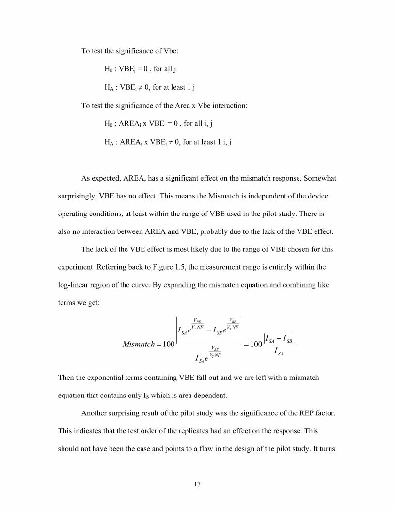
To test the significance of Vbe:
H0 : VBEj = 0 , for all j
HA : VBEi ≠ 0, for at least 1 j
To test the significance of the Area x Vbe interaction:
H0 : AREAi x VBEj = 0 , for all i, j
HA : AREAi x VBEi ≠ 0, for at least 1 i, j
As expected, AREA, has a significant effect on the mismatch response. Somewhat
surprisingly, VBE has no effect. This means the Mismatch is independent of the device
operating conditions, at least within the range of VBE used in the pilot study. There is
also no interaction between AREA and VBE, probably due to the lack of the VBE effect.
The lack of the VBE effect is most likely due to the range of VBE chosen for this
experiment. Referring back to Figure 1.5, the measurement range is entirely within the
log-linear region of the curve. By expanding the mismatch equation and combining like
terms we get:
SA
SBSA
NFVV
SA
NFVV
SBNFV
V
SA
III
eI
eIeI
MismatchT
BE
T
BE
T
BE
−=
−
= 100100
Then the exponential terms containing VBE fall out and we are left with a mismatch
equation that contains only IS which is area dependent.
Another surprising result of the pilot study was the significance of the REP factor.
This indicates that the test order of the replicates had an effect on the response. This
should not have been the case and points to a flaw in the design of the pilot study. It turns
17

out there are a number of factors that may have caused REP to have an effect: The lack of
randomization; No control over the temperature of the replicates; perhaps the test
equipment developed an offset over the course of the experiment. This result stresses the
importance of randomization when performing experiments.
3.3. Simplified Statistical model
The initial results of the pilot study indicate that the factors for VBE and the
AREA-VBE interaction can be dropped from the model, as they are not significant. The
simplified effects model becomes:
ikkiik REPAREAy εµ +++= ; i=1,2,3 k=1,2,…,52
subject to the constraint:
0=∑i
iAREA
εik iid N(0, σ2)
The hypotheses being tested are the same as before:
H0 : AREAi = 0 , for all i
HA : AREAi ≠ 0, for at least 1 i
The SAS procedure GLM was used to perform the analysis with the results of the
analysis shown in Table 3.3. For the simplified model we have:
Replicates REP = { 1 2 … 52 }
3 level of Area AREA = { 1 5 10 }
18
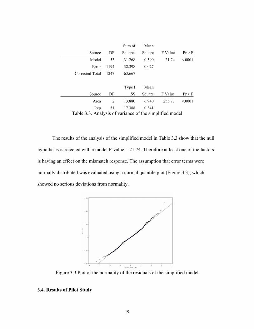
Sum of Mean Source DF Squares Square F Value Pr > F Model 53 31.268 0.590 21.74 <.0001 Error 1194 32.398 0.027
Corrected Total 1247 63.667 Type I Mean
Source DF SS Square F Value Pr > F Area 2 13.880 6.940 255.77 <.0001 Rep 51 17.388 0.341
Table 3.3. Analysis of variance of the simplified model
The results of the analysis of the simplified model in Table 3.3 show that the null
hypothesis is rejected with a model F-value = 21.74. Therefore at least one of the factors
is having an effect on the mismatch response. The assumption that error terms were
normally distributed was evaluated using a normal quantile plot (Figure 3.3), which
showed no serious deviations from normality.
Figure 3.3 Plot of the normality of the residuals of the simplified model
3.4. Results of Pilot Study
19

The pilot study showed that factors for VBE and the AREA-VBE interaction had
no effect and that the proposed model could be simplified to:
ikkiik REPAREAy εµ +++= ; i = 1, 2, 3 k = 1, 2, …, 52
subject to the constraints:
0=∑i
iAREA
εij iid N(0, σ2)
The surprising effect of REP led to changes in the setup of the final run of the
experiment. Modifications to the setup for the final run of the experiment:
1. Randomize the test order of the replicates
2. Randomize the test order of the “A” and “B” devices in each transistor pair
3. Keep the temperature constant throughout the experiment
3.5. Sample Size Calculation for Final Run.
To determine the sample size needed for the final run, the data from the pilot
study were randomly shuffled and reordered. The reordered data were resampled without
replacement for sample sizes ranging from 2 to 52 and analyzed using a SAS macro,
which can be found in Appendix A.3. The margin of error (using α=0.05) was calculated
for each of 25 resamplings. Figure 3.4 displays the average and maximum margin as a
function of sample size. Thus for a margin of error of 0.5 which is typical for this
application, it can be seen that the pilot study sample size of 52 was more than adequate.
It should be noted that any sample size greater than 10 or so would have a sufficiently
low margin of error for the final run of the experiment.
20
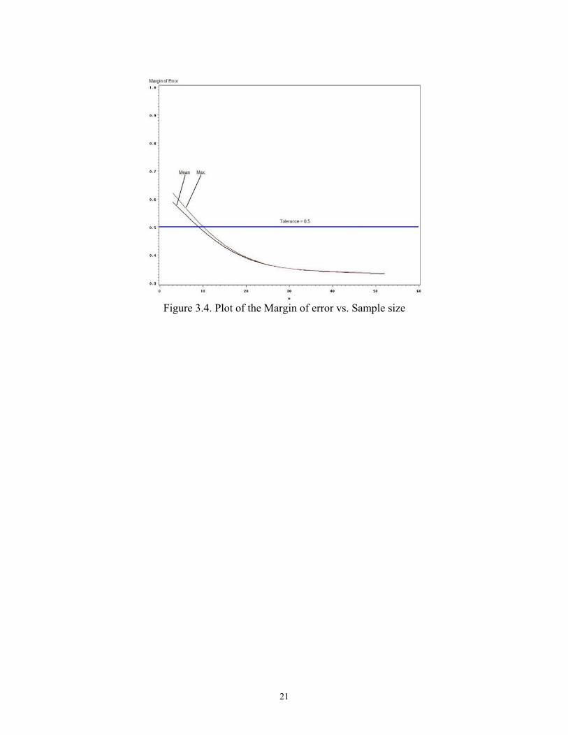
Figure 3.4. Plot of the Margin of error vs. Sample size
21

4. Final Run
4.1. Design of the Final Run
The test circuit and test method for the final run were the same as those for the
pilot study. Changes to the setup of the experiment were noted above in section 3.4.
Namely, the test order of the replicates was randomized for the experiment and the
temperature was controlled and held constant at 25°C.
The pilot study showed that the sample size could be reduced and we would still
achieve the desired level of confidence in the model, therefore the sample size was
reduced to 42 replicates. Figure 4.1 shows the experimental wafer with the test order of
the replicates.
Figure 4.1 Test order of the replicates for the final run of the experiment
The test order for each device in the matched pair was also randomized. The only
constraint was that both devices of a matched pair were tested sequentially. For example,
if the Area10 device ‘B’ was tested first, then Area10 device ‘A’ was tested next.
22

Test Order Test Order Replicate ID 1_A 1_B 5_A 5_B 10_A 10_B
Replicate ID 1_A 1_B 5_A 5_B 10_A 10_B
1 R8C8 4 3 2 1 6 5 22 R8C4 2 1 6 5 4 3 2 R9C5 1 2 4 3 6 5 23 R7C8 5 6 1 2 4 3 3 R6C7 1 2 4 3 5 6 24 R9C7 5 6 3 4 1 2 4 R8C7 4 3 2 1 6 5 25 R3C6 5 6 2 1 3 4 5 R4C6 6 5 3 4 1 2 26 R9C8 3 4 2 1 5 6 6 R8C3 2 1 6 5 3 4 27 R6C8 2 1 6 5 4 3 7 R4C8 4 3 1 2 6 5 28 R4C4 1 2 3 4 5 6 8 R9C6 5 6 4 3 1 2 29 R4C3 5 6 2 1 4 3 9 R3C3 4 3 5 6 2 1 30 R7C5 4 3 5 6 2 1
10 R3C4 4 3 2 1 5 6 31 R6C3 1 2 6 5 4 3 11 R8C5 2 1 6 5 4 3 32 R5C8 2 1 4 3 5 6 12 R3C7 5 6 2 1 3 4 33 R7C3 6 5 3 4 2 1 13 R9C3 5 6 2 1 3 4 34 R3C8 4 3 2 1 5 6 14 R5C5 3 4 1 2 6 5 35 R6C5 3 4 2 1 6 5 15 R7C4 1 2 3 4 5 6 36 R7C6 5 6 4 3 1 2 16 R3C5 1 2 3 4 5 6 37 R6C4 6 5 1 2 4 3 17 R5C3 6 5 1 2 3 4 38 R9C4 1 2 4 3 5 6 18 R6C6 2 1 6 5 3 4 39 R5C4 3 4 1 2 5 6 19 R4C7 4 3 5 6 2 1 40 R7C7 1 2 5 6 3 4 20 R4C5 5 6 3 4 1 2 41 R8C6 4 3 1 2 5 6 21 R5C6 1 2 6 5 4 3 42 R5C7 5 6 2 1 4 3
Table 4.1 Test order of the replicates in the final run of the experiment
4.2. Analysis and Final Results
The data from the final run was analyzed using the simplified model developed in
the pilot study. The effects model for the final run is:
ijjiij REPAREAy εµ +++=
subject to the constraint:
0=∑i
iAREA , i=1, 2, 3
εij iid N(0, σ2)
23

Checking the significance of the model by looking at the normality of the
residuals revealed the presence of outliers in the data
4.2 Plot of the normality of the residuals
Taking a closer look at the outliers showed that the most extreme were from row
3 on the experimental wafer as well as from replicate 40. The fact that every replicate in
row 3 was an outlier points to a defect caused by something specific rather than a random
defect. It is not uncommon for problems in manufacturing to affect large areas of the
wafer. A problem with one of the masking steps could have easily caused this type of
defect. Replicate 40 may have encountered a problem during testing.
Lowest Residuals
Highest Residuals
Rep Row Col Area resid Rep Row Col Area resid 40 R7 C7 5 -0.4343 10 R3 C4 5 0.4659 40 R7 C7 5 -0.4336 25 R3 C6 5 0.4789 40 R7 C7 5 -0.4272 40 R7 C7 1 0.5585 40 R7 C7 5 -0.4073 40 R7 C7 1 0.5622 40 R7 C7 5 -0.4065 40 R7 C7 1 0.5646 40 R7 C7 5 -0.3925 25 R3 C6 5 0.6059 8 R9 C6 1 -0.3735 40 R7 C7 1 0.6135 8 R9 C6 1 -0.3705 40 R7 C7 1 0.6186 8 R9 C6 1 -0.3698 40 R7 C7 1 0.6223
40 R7 C7 5 -0.3639 40 R7 C7 1 0.6236 25 R3 C6 1 -0.3617 40 R7 C7 1 0.6415 8 R9 C6 1 -0.3577 16 R3 C5 5 0.7017
24

Table 4.2 Highest and lowest residuals
Figure 4.3 Location of the final run outliers
Removing the outliers from the dataset reduced the number of replicates to thirty-
five, still more than necessary for a tolerance of 0.5 with α=0.05 from Figure 3.5. The
ANOVA of the reduced data set is shown in Table 4.3. Checking the significance of the
model with the hypotheses:
H0 : AREAi = 0 , for all i
HA : AREAi ≠ 0, for at least 1 i
Sum of Mean
Source DF Squares Square F Value Pr > F
Model 36 24.608 0.684 37.83 <.0001
Error 803 14.510 0.018
Corrected Total 839 39.119
Type I Mean
Source DF SS Square F Value Pr > F
AREA 2 17.877 8.938 494.65 <.0001
REP 34 6.732 0.198 Table 4.3 Analysis of variance for the final run with outliers removed
25

Table 4.3 shows that the null hypothesis is rejected with the F-value of the model
equal to 37.83 with a corresponding P-value <0.0001. Therefore at least one of the
blocking factors, either AREA or REP, is having an effect on the mismatch response.
With the observations identified as outliers removed, the residuals appear to be much
more consistent with a normal distribution.
4.4 Plot of the normality of the residuals
with the outliers removed
Checking for the significance of AREA with the hypotheses:
H0 : AREAi = 0 , for all i
HA : AREAi ≠ 0, for at least 1 i
From table 4.2 it can be seen that AREA is significant with an F-value of 494.65
and P-value <0.0001. The non-zero value of the REP mean square seems to indicate that
there is still something significant with the replicate number. Its effects are being
accounted for by using REP as a blocking factor.
26

4.3 Lookup Table
Circuit designers need information in a format that’s easy to use and understand.
Typically, circuits in which mismatch is critical are designed to tolerate a specified
maximum level of device mismatch. A lookup table that displays the prediction intervals
for new observations for each size of device was determined to be the best way to display
the results of this project.
Because ( )( )22)( ˆ, σσ +≈ AREAAREAnewAREA yyNy
( ) αα ≈++> MSEyszyyP AREAAREAnewAREA )ˆ(ˆ 2)(
Thus the look-up table (See Table 4.4) gives values of MSEyszy AREAAREA ++ )ˆ(ˆ 2α for
various levels of AREA and α. For example, for AREA=1 and α=0.05 we would expect
absolute mismatch to exceed 0.6668 only 5% of the time.
Area Predicted α=0.10 α=0.05 α=0.01 1 0.4451 0.6179 0.6668 0.7586 5 0.1414 0.3142 0.3631 0.4549 10 0.1302 0.3030 0.3519 0.4437
Table 4.4 Look-up Table
27

5. Conclusions
Statistical modeling provides a useful tool in the estimation of important bipolar
device parameters. It can also be used to identify non-essential factors, in this case VBE,
so they can be eliminated from consideration. The importance of randomization in
experimental design cannot be overlooked as shown by the large REP effect in the pilot
study. An effects model was developed without special knowledge of the manufacturing
process making this method useful to users who may not have access to this information.
The method presented in this paper can easily be extended and modified to other device
types such as PNP and CMOS devices.
28

6. References P. G. Drenan (2002) Device Mismatch in BiCMOS Technologies, IEEE Proceedings of the Bipolar/BiCMOS Circuits and Technology Meeting pp.l04-110. P.G. Drennan, C.C. McAndrew, J. Bates (1998) A Comprehensive Vertical BJT Mismatch Model, IEEE Proceedings of the Bipolar/BiCMOS Circuits and Technology Meeting. H. Holer (2000) Measurement and Mismatch modeling of Semiconductor devices in BiCMOS Technology, IEEE Symposium on Circuit and Systems. D. C. Montgomery (2000) Design and Analysis of Experiments, 5th Edition, Wiley. J. Neter, M. H Kutner, W. Wasserman, C. J. Nachtsheim (1996) Applied Linear Statistical Models, 4th Edition, McGraw-Hill/Irwin. T. Ngo, R. Hester, A. Fok, B. Abdi, M. Rencher, B. Burns, I. Miller, (1990) A Process and Geometry Driven Device Macro Model for Statistical Simulation of Bipolar ICs, IEEE Symposium on Circuits and Systems. pp. 85-88. A. Pergoot, B. Graindourze, Er. Janssens, J. Bastos, M. Steyaert, P. Kinget, R. Roovers, W. Sansen, Statistics for Matching (1995) Proceedings of the IEEE International Conference on Microelectronic Test Structures, Vol. 8.
29

Appendix A.1. SAS code for the analysis of the pilot study * ******************************************************************** ; * Pilot Study Analysis Program ; * ; * This program develops a model for the pilot study data. ; * ; * Looked for main effects: ; * Area ; * VBE ; * Replicate - This should NOT have ant effect, but since the ; * test order of the replicates was not randomized ; * in the pilot study we need to check. ; * ; * Interaction: ; * Area x VBE There is some evidence from past experiments that ; * this interaction is real ; * ; * Response ; * ; * Mismatch% = 100*|(ICa - ICb)| / ICa ; * ; * Model ; * ; * Initial: ; * y = u + AREA + VBE + REP + (AREA x VBE) + e ; * Final ; * y = u + AREA + REP + e ; * ; * ******************************************************************** ; * Import excel workbook containing the pilot study data ; PROC IMPORT OUT= Expdata DATAFILE= "pilotdata.xls" DBMS=EXCEL2000 REPLACE; GETNAMES=YES; RUN; * reset titles ; title " "; title2 " "; * sort data by factors; proc sort data=Expdata; by area vbe rep; run; * Part 1: fit model using area, vbe, replicate number, ; * and area-vbe interaction ; title "Pilot Study Preliminary Model"; proc glm data=Expdata; class area vbe rep; model mismatch=area vbe rep area*vbe; output out=mod_out p=pred r=resid stdi=std_err_pred; run;
30
* check normality of residuals; proc univariate data=mod_out normal; var resid; qqplot /normal(MU=EST SIGMA=EST) ; run; * ******************************************************************** ; * Part 2: Fit the simplified model ; * vbe and the area-vbe have no effect so remove them ; * from the model and run it again ; * ******************************************************************** ; title "Pilot Study Simplified Model"; proc glm data=Expdata; class area rep; model mismatch=area rep; output out=mod_out p=pred r=resid stdi=std_err_pred; run; * check normality of residuals; proc univariate data=mod_out normal; var resid; qqplot /normal(MU=EST SIGMA=EST) ; run; ***********************************************************************; * ; * END PROGRAM ; * ; ***********************************************************************;
31

Appendix A.2. SAS code for determining the sample size * ******************************************************************** ; * Pilot Study Analysis Program 2 ; * finalrun_samp_size.sas ; * ; * This program uses the model developed in Pilotstudy1 and ; * calculates the standard error of the predicted value (sep) and ; * margin of error (moe) for increasing sample sizes ; * ; * This will be used to determine the sample size for the final run ; * ; * Model ; * Mismatch = 100 * |(ICa - ICb)| / ICa ; * Mismatch = u + AREA + VBE + REP + e ; * ; * AREA and VBE are discrete variables ; * ; * ******************************************************************** ; * Import excel workbook containing the pilot study data ; PROC IMPORT OUT= pilotdata DATAFILE= "pilotdata.xls" DBMS=EXCEL2000 REPLACE; GETNAMES=YES; RUN; * The macro m_sep uses the GLM procedure to calculate standard error ; * of the predicted value (sep) and margin of error (moe) of the ; * Pilotdata for the given sample size ; %macro m_sep(sampsize= ); * fit model ; proc glm data=Pilotdata noprint; class Vbe Area Rep; model mismatch=Vbe Area Rep; output out=tempmod p=pred r=resid stdi=sep; where newrep <= &sampsize; * only fits the first ; * &samplesize records in each ; * vbe x area combination ; run; * calculate the margin of error (moe) ; data tempmod; set tempmod; moe=1.96*sep; * half-width of confidence interval, ; * alpha=0.05 ; run; * get mean, min, and max values of moe ; proc means data=tempmod noprint; var moe; output out=temp9 min=min max=max mean=mean; ****HERE**** ; run; %mend m_sep;
32

* return the sample size so it can be added to the title ; %macro ssize(sampsize= ); &sampsize; %mend ssize; %macro width; data newtemp; run; %do iperm = 1 %to 25; * number of random reorderings ; data pilotdata; set pilotdata; random=ranuni(0); * Assign a random number to each record ; run; proc sort data=pilotdata; * sort by random number (randomize) ; by Vbe Area random; * within each (VBE x AREA) combination ; run; data pilotdata; set pilotdata; newrep=int((_n_-1)/24)+1; * new rep number within each ; run; * VBE x AREA combination ;
* consider each sample size (within vbe x area combination) ; * from n=2 to n=52 one at a time ; %do i = 2 %to 52 ; %m_sep(sampsize=&i); * estimate margin of error ; data newtemp; set newtemp temp9; * saves output from ****HERE**** ; run; %end; * for i ; run; %end; * for iperm ; run; %mend; * width ; * do width macro; %width data newtemp; * Dataset with results from previous steps ; * (estimated margins of error) ; set newtemp; n=_FREQ_/24; * sample size corresponding to each margin of ; * error listed in the dataset ; run; proc sort data=newtemp; by n; run; symbol1 v=none c=black i=sm70; symbol2 v=none c=red i=sm70;
33

symbol3 v=none c=blue i=sm70; title "Margin of Error vs Sample Size"; proc gplot data=newtemp; plot (mean max)*n/overlay; where n gt 1; run; ***********************************************************************; * ; * END PROGRAM ; * ; ***********************************************************************;
34

Appendix A.3. SAS code for the analysis of the final run * ****************************************************************** ; * Final Run Analysis Program ; * ; * This program fits the model developed in the pilot study to the ; * experimental data. The factor VBE and the (Area x VBE) ; * interaction have been dropped as they had no effect ; * ; * Part 2 checks the constancy of the error variance using the ; * modified levene test. ; * ; * Looked for main effects: ; * Area ; * Replicate - This should NOT have ant effect, but since the test ; * order of the replicates was not randomized in the ; * pilot study we need to check. ; * ; * Response ; * ; * Mismatch% = 100 * |(ICa - ICb)| / ICa ; * ; * Model ; * ; * y = u + AREA + REP + e ; * ; * ****************************************************************** ; * Import excel workbook containing the final run data ; PROC IMPORT OUT= Expdata DATAFILE= "finalrundata.xls" DBMS=EXCEL2000 REPLACE; GETNAMES=YES; RUN; * reset titles ; title " "; title2 " "; * ****************************************************************** ; * Part 1: Fit the model to the entire data set ; * ; * ****************************************************************** ; * sort data before doing proc glm; proc sort data=Expdata; by area rep; run; * fit model using area and replicate number; title "Final run model"; proc glm data=Expdata; class area rep; model mismatch=area rep; output out=mod_out p=pred r=resid stdi=std_err_pred;
35

36
run; * check normality of residuals; *symbol v=dot c=black i=none; title "Normality of the residuals of the final model"; proc univariate data=mod_out normal; var resid; qqplot /normal(MU=EST SIGMA=EST) ; run; * fit model using area and replicate number; title "Final run model with outliers removed"; proc glm data=Expdata; class area rep; model mismatch=area rep; output out=mod_out_no_outlier p=pred r=resid stdi=std_err_pred; where ((rep ne 40) and (ROW ne "R3")); lsmeans area/stderr; run; * check normality of residuals; *symbol v=dot c=black i=none; title "Normality of the residuals with outliers removed"; proc univariate data=mod_out_no_outlier normal; var resid; qqplot /normal(MU=EST SIGMA=EST) ; run; ******************************************************************** ; * ; * END PROGRAM ; * ; ******************************************************************** ;