total dose and dose rate models for bipolar … · 2. structure of an npn bipolar transistor ......
TRANSCRIPT
SANDIA REPORT SAND2013-3769 Unlimited Release Printed May 2013
Total Dose and Dose Rate Models for Bipolar Transistors in Circuit Simulation Philip M. Campbell and Steven D. Wix Prepared by Sandia National Laboratories Albuquerque, New Mexico 87185 and Livermore, California 94550
Sandia National Laboratories is a multi-program laboratory managed and operated by Sandia Corporation, a wholly owned subsidiary of Lockheed Martin Corporation, for the U.S. Department of Energy's National Nuclear Security Administration under contract DE-AC04-94AL85000.
Approved for public release; further dissemination unlimited.

2
Issued by Sandia National Laboratories, operated for the United States Department of Energy by Sandia Corporation. NOTICE: This report was prepared as an account of work sponsored by an agency of the United States Government. Neither the United States Government, nor any agency thereof, nor any of their employees, nor any of their contractors, subcontractors, or their employees, make any warranty, express or implied, or assume any legal liability or responsibility for the accuracy, completeness, or usefulness of any information, apparatus, product, or process disclosed, or represent that its use would not infringe privately owned rights. Reference herein to any specific commercial product, process, or service by trade name, trademark, manufacturer, or otherwise, does not necessarily constitute or imply its endorsement, recommendation, or favoring by the United States Government, any agency thereof, or any of their contractors or subcontractors. The views and opinions expressed herein do not necessarily state or reflect those of the United States Government, any agency thereof, or any of their contractors. Printed in the United States of America. This report has been reproduced directly from the best available copy. Available to DOE and DOE contractors from U.S. Department of Energy Office of Scientific and Technical Information P.O. Box 62 Oak Ridge, TN 37831 Telephone: (865) 576-8401 Facsimile: (865) 576-5728 E-Mail: [email protected] Online ordering: http://www.doe.gov/bridge Available to the public from U.S. Department of Commerce National Technical Information Service 5285 Port Royal Rd. Springfield, VA 22161 Telephone: (800) 553-6847 Facsimile: (703) 605-6900 E-Mail: [email protected] Online ordering: http://www.ntis.gov/ordering.htm
3
SAND2013-3769 Unlimited Release Printed May 2013
Total Dose and Dose Rate Models for Bipolar Transistors in Circuit Simulation
Philip M. Campbell Scientific Computing Systems
Steven D. Wix Component Information and Models
Sandia National Laboratories P.O. Box 5800
Albuquerque, New Mexico 87185-0525
Abstract The objective of this work is to develop a model for total dose effects in bipolar junction transistors for use in circuit simulation. The components of the model are an electrical model of device performance that includes the effects of trapped charge on device behavior, and a model that calculates the trapped charge densities in a specific device structure as a function of radiation dose and dose rate. Simulations based on this model are found to agree well with measurements on a number of devices for which data are available.
4
ACKNOWLEDGMENTS
The authors are grateful to Nathan Nowlin for many helpful comments and for pointing us to important early references.

5
CONTENTS
1. Introduction ................................................................................................................................ 9
2. Structure of an NPN Bipolar Transistor ................................................................................... 11
3. Trends in the Data .................................................................................................................... 13
4. The Effect of Oxide-Trapped Charge – Spread of the Depletion Region................................ 15
5. Analysis of Surface Recombination and a Model for Excess Base Current ............................ 17
6. Comparison of Model with Experiment .................................................................................. 21
7. Structure of the PNP Bipolar Transistor .................................................................................. 23
8. Model for Dose Rate Sensitivity of Trapped Charge............................................................... 25
9. Comparing Simulation with Measurements for the 2N2222 and 2N2907 .............................. 29
10. Measurement and Simulation for Lateral and Substrate PNPs .............................................. 31
11. Summary and Conclusions .................................................................................................... 35
REFERENCES ............................................................................................................................. 37
APPENDIX A Verilog-A Model for 2N2222 with TD Effects ................................................... 39
APPENDIX B Verilog-A Model for 2N2907 with TD Effects ................................................... 47
APPENDIX C Verilog-A Model for LPNP and SPNP Devices with TD Effects ....................... 55
APPENDIX D ELDRS Model for Trapped Charge in 2N2222 and 2N2907 .............................. 63
APPENDIX E ELDRS Model for Trapped Charge in LPNP and SPNP Devices ....................... 71
DISTRIBUTION........................................................................................................................... 79
6
FIGURES
Figure 1. Structure of a substrate NPN bipolar transistor. ........................................................... 11 Figure 2. Excess base current versus base-emitter voltage showing transition points where the
recombination rate moves below the surface and into the bulk. ............................................. 13 Figure 3. Excess base current versus positive oxide charge showing saturation effect. .............. 14 Figure 4. Sufficient oxide-trapped charge is present to extend the depletion region throughout
the intrinsic base. .................................................................................................................... 15 Figure 5. Assumed structure of the emitter/intrinsic-base region. ............................................... 18 Figure 6. Assumed shape of the lateral distribution of recombination current. ........................... 18 Figure 7. Measured excess base current compared with model calculations [9]. ........................ 22 Figure 8. Structure of (a) vertical, (b) lateral, and (c) substrate PNP transistors. ........................ 23 Figure 9. Expansion of depletion region into the emitter from oxide-trapped charge in a PNP
device. ..................................................................................................................................... 24 Figure 10. Measurement and simulation of the dose-rate effect in 2N2222 and 2N2907 at VBE =
0.5 V. ....................................................................................................................................... 29 Figure 11. Measurement and simulation of the dose-rate effect in two PNP devices at VBE = 0.7
V. ............................................................................................................................................. 31 Figure 12. Excess base current in the lateral device versus base-emitter voltage from which
transition points, trV , can be derived. ..................................................................................... 32
TABLES
Table 1. Simulation Parameters for Devices Tested. ................................................................... 30 Table 2. Areal Density Values for Oxice-Trapped Charge and Interface-Trapped Charge. ....... 32

7
NOMENCLATURE
BJT bipolar junction transistor cgs centimeter-gram-second ELDRS enhanced low dose rate sensitivity LPNP lateral PNP MOS metal oxide semiconductor MOSFET metal-oxide semiconductor field-effect transistor NPN negative-positive-negative (transistor) PNP positive-negative-positive (transistor) SNL Sandia National Laboratories SnPb tin-lead SPICE Simulation Program with Integrated Circuit Emphasis, a circuit simulator SPNP substrate PNP SRAM static random-access memory VPNP vertical PNP WR war reserve

8

9
1. INTRODUCTION
Earlier, a total dose model was developed for metal-oxide semiconductor field-effect transistors (MOSFETs) that allows one to analytically predict values for oxide-trapped charge and interface-trapped charge for a given radiation dose [1]. The effects of trapped charge on device characteristics are a shift in threshold voltage and a modification of channel mobility. Experimental data on a number of metal oxide semiconductor (MOS) devices were analyzed successfully with this model, which has been included in the Xyce circuit simulation code.
In this report a comparable model for bipolar junction transistors (BJTs) is discussed. Total dose effects in BJTs are much different than in MOSFETs. The emitter-base junction in BJTs is covered by an oxide layer referred to as the base oxide. This oxide is usually of much lower quality than the gate oxides in MOSFETs because of the BJT fabrication process. In addition, the fields in the gate oxide of MOSFETs are on the order of 1 MV/cm while the fields in the base oxide of a BJT are normally much less than 0.1 MV/cm. Electron-hole recombination plays a more dominant role in an oxide with small fields. Most significantly, BJTs exhibit dose-rate effects (enhanced low dose rate sensitivity, ELDRS) whereas MOSFETs in most cases do not [2] [3] (a possible exception is the radiation-sensing field effect transistor [RADFET]).
The model for total dose effects presented here has two components. The first is an electrical model of device performance that includes the effects of trapped charge on device behavior, and the second is a model that calculates the trapped charge densities in a specific device structure as a function of radiation dose and dose rate. Trapped charge in BJTs has two main effects: (1) a spread in the emitter-base depletion region caused by oxide-trapped charge, and (2) an increase in the surface recombination velocity from interface-trapped charge. These two effects result in an excess base current that follows from increased surface recombination. In the presence of trapped charge, holes reaching the surface in the p-doped base of a negative-positive-negative (NPN) transistor recombine more rapidly. The resulting diffusion current of holes into the region appears externally as an excess base current. Excess base current, BI∆ , lowers the transistor gain, ( )BBC III ∆+/ . In the following section an electrical model is discussed that includes the effects of trapped charge on device performance. This model, which requires values of trapped charge as input parameters, is implemented in Verilog-A (see Appendices A – C).
A number of different processes have been identified as contributing to the dose-rate effect under different conditions [4] [5], probably between 10 and 20. In this report a first-order model for ELDRS is presented that includes seven of the physics effects considered to be most important. The current model is considered a first-order effort because it treats the oxide as “thin.” In other words, the space distribution of carriers in the oxide is neglected along with some transport effects. In addition, a simplified model for the oxide field is used that neglects some of the more complex issues in the oxide field calculation. Future work needs to focus on a more precise treatment of transport and space charge effects (Poisson’s equation), and some additional hydrogen reactions that occur in association with interface trap formation need to be included.

10
11
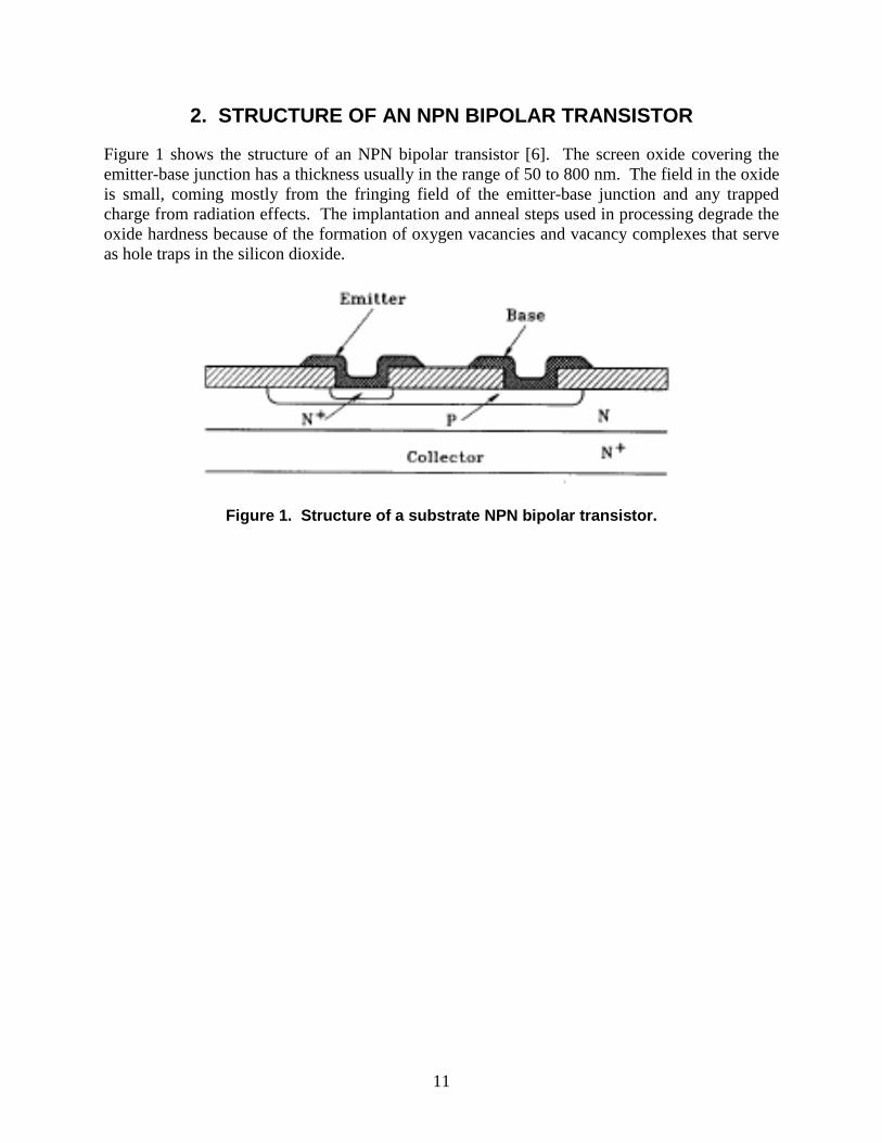
2. STRUCTURE OF AN NPN BIPOLAR TRANSISTOR
Figure 1 shows the structure of an NPN bipolar transistor [6]. The screen oxide covering the emitter-base junction has a thickness usually in the range of 50 to 800 nm. The field in the oxide is small, coming mostly from the fringing field of the emitter-base junction and any trapped charge from radiation effects. The implantation and anneal steps used in processing degrade the oxide hardness because of the formation of oxygen vacancies and vacancy complexes that serve as hole traps in the silicon dioxide.
Figure 1. Structure of a substrate NPN bipolar transistor.

12
13
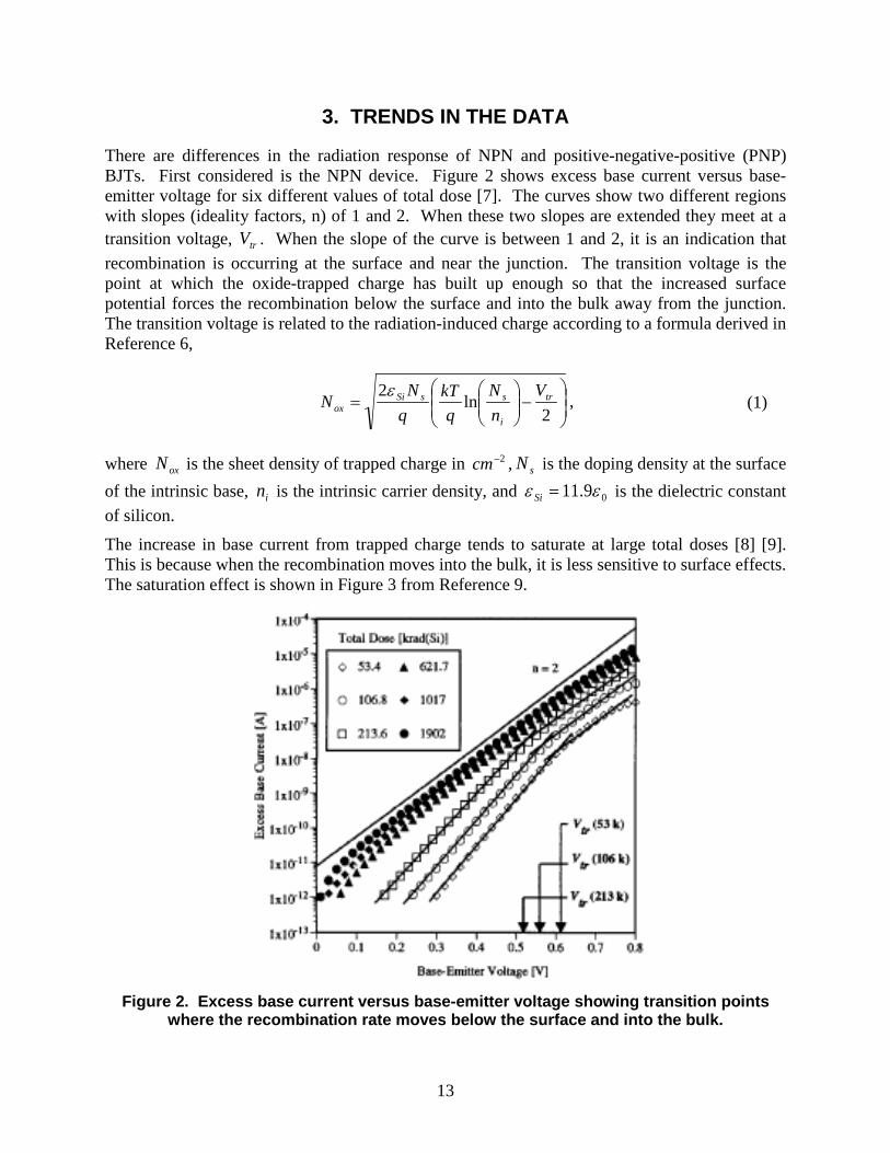
3. TRENDS IN THE DATA
There are differences in the radiation response of NPN and positive-negative-positive (PNP) BJTs. First considered is the NPN device. Figure 2 shows excess base current versus base-emitter voltage for six different values of total dose [7]. The curves show two different regions with slopes (ideality factors, n) of 1 and 2. When these two slopes are extended they meet at a transition voltage, trV . When the slope of the curve is between 1 and 2, it is an indication that recombination is occurring at the surface and near the junction. The transition voltage is the point at which the oxide-trapped charge has built up enough so that the increased surface potential forces the recombination below the surface and into the bulk away from the junction. The transition voltage is related to the radiation-induced charge according to a formula derived in Reference 6,
−
=
2ln
2 tr
i
ssSiox
VnN
qkT
qN
Nε , (1)
where oxN is the sheet density of trapped charge in 2−cm , sN is the doping density at the surface of the intrinsic base, in is the intrinsic carrier density, and 09.11 εε =Si is the dielectric constant of silicon.
The increase in base current from trapped charge tends to saturate at large total doses [8] [9]. This is because when the recombination moves into the bulk, it is less sensitive to surface effects. The saturation effect is shown in Figure 3 from Reference 9.
Figure 2. Excess base current versus base-emitter voltage showing transition points
where the recombination rate moves below the surface and into the bulk.

14
Figure 3. Excess base current versus positive oxide charge showing saturation effect.

15
4. THE EFFECT OF OXIDE-TRAPPED CHARGE – SPREAD OF THE DEPLETION REGION
Because the oxide-trapped charge is positive, the depletion region in an NPN device spreads into the relatively lightly doped p-type base region, as shown in Figure 4. This is because the trapped charge in the oxide repels holes in the base. In a PNP device, the oxide charge expands the depletion region into the emitter.
At the transition voltage corresponding to a certain total dose as shown in Figure 2, sufficient oxide-trapped charge has accumulated to cause recombination to occur throughout the intrinsic base. Once this has happened, the excess base current is proportional to the area of the intrinsic base, as shown in Figure 4. After this point, the effect of trapped charge has saturated and further increases in BI∆ will be small.
Figure 4. Sufficient oxide-trapped charge is present to extend the depletion region
throughout the intrinsic base.

16

17
5. ANALYSIS OF SURFACE RECOMBINATION AND A MODEL FOR EXCESS BASE CURRENT
The excess base currents can be derived from Shockley-Read-Hall recombination theory [10]. The model is derived in Reference 9. The model assumes a rectangular shape for the emitter/intrinsic-base structure, as shown in Figure 5. The variation of recombination rate in the vicinity of the emitter-base junction is somewhat complicated, as demonstrated in Reference 9, so in order to get an analytical solution, a simplified form for the recombination rate versus lateral position is assumed, as shown in Figure 6. With these simplifications, the recombination rate can be integrated over the area of the intrinsic base to obtain
( ) ×
=∆
kTqV
PvqnsurfI beEsurfiB 2
exp5.0
++∆
kTqV
NLN
PL
NLn
L be
sD
ox
E
IB
s
IBi
2exp
2exp
41
22
. (2)
In this expression, intNvv thsurf σ= is the surface recombination velocity, with σ the capture cross section, thv the thermal velocity, and intN the density of trapping centers at the interface. The perimeter of the emitter is EP , and IBL is the extent of the intrinsic base, as shown in Figure 5. oxN is the sheet density of oxide-trapped charge, in is the intrinsic density, and sN is the doping density at the surface of the intrinsic base. L∆ is as shown in Figure 6, but is not
precisely defined. beV is the base-emitter voltage drop, and the Debye length is s
siD Nq
kTL 2
ε= .
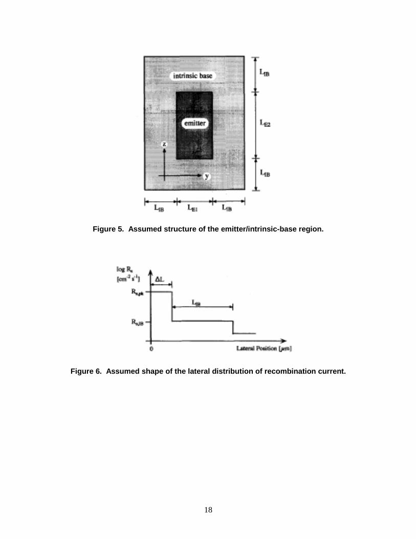
18
Figure 5. Assumed structure of the emitter/intrinsic-base region.
Figure 6. Assumed shape of the lateral distribution of recombination current.
19
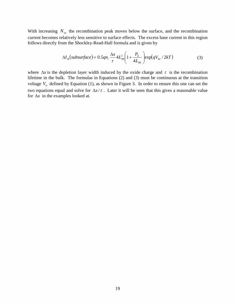
With increasing oxN the recombination peak moves below the surface, and the recombination current becomes relatively less sensitive to surface effects. The excess base current in this region follows directly from the Shockley-Read-Hall formula and is given by
( ) ( )kTqV
LPLxqnsubsurfaceI be
IB
EIBiB 2/exp
4145.0 2
+
∆=∆
τ (3)
where x∆ is the depletion layer width induced by the oxide charge and τ is the recombination lifetime in the bulk. The formulas in Equations (2) and (3) must be continuous at the transition voltage trV defined by Equation (1), as shown in Figure 3. In order to ensure this one can set the two equations equal and solve for τ/x∆ . Later it will be seen that this gives a reasonable value for x∆ in the examples looked at.

20
21
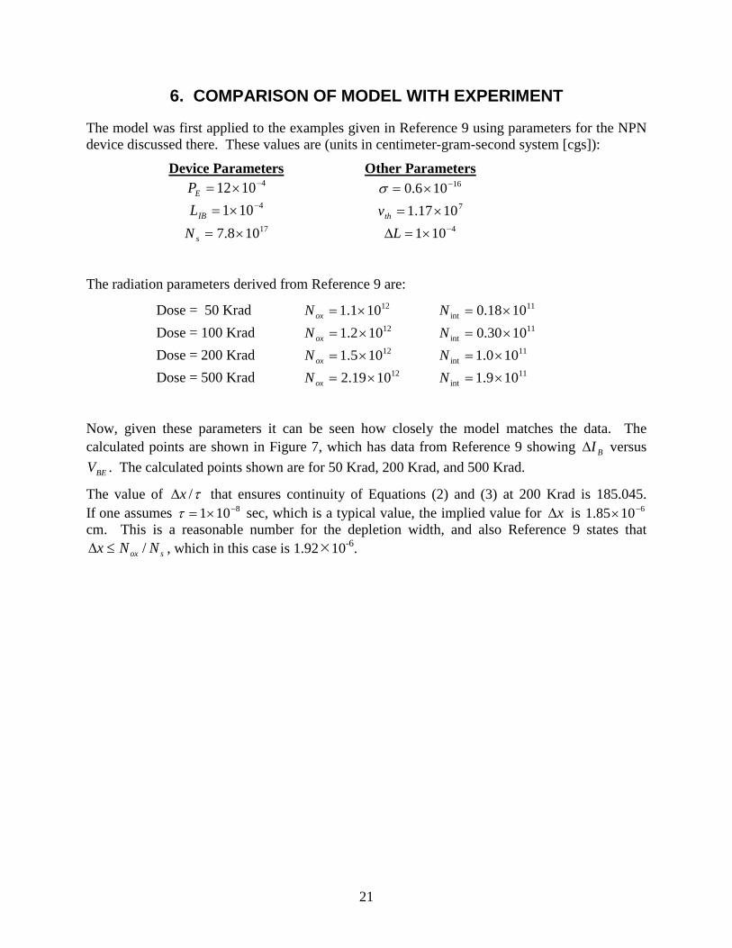
6. COMPARISON OF MODEL WITH EXPERIMENT
The model was first applied to the examples given in Reference 9 using parameters for the NPN device discussed there. These values are (units in centimeter-gram-second system [cgs]):
Device Parameters Other Parameters 41012 −×=EP 16106.0 −×=σ 4101 −×=IBL 71017.1 ×=thv 17108.7 ×=sN 4101 −×=∆L
The radiation parameters derived from Reference 9 are:
Dose = 50 Krad 12101.1 ×=oxN 11int 1018.0 ×=N
Dose = 100 Krad 12102.1 ×=oxN 11int 1030.0 ×=N
Dose = 200 Krad 12105.1 ×=oxN 11int 100.1 ×=N
Dose = 500 Krad 121019.2 ×=oxN 11int 109.1 ×=N
Now, given these parameters it can be seen how closely the model matches the data. The calculated points are shown in Figure 7, which has data from Reference 9 showing BI∆ versus
BEV . The calculated points shown are for 50 Krad, 200 Krad, and 500 Krad.
The value of τ/x∆ that ensures continuity of Equations (2) and (3) at 200 Krad is 185.045. If one assumes 8101 −×=τ sec, which is a typical value, the implied value for x∆ is 61085.1 −× cm. This is a reasonable number for the depletion width, and also Reference 9 states that
sox NNx /≤∆ , which in this case is 1.9210-6.
22
Figure 7. Measured excess base current compared with model calculations [9].
23
7. STRUCTURE OF THE PNP BIPOLAR TRANSISTOR
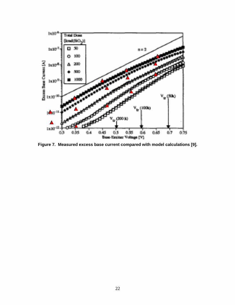
Three basic types of PNP bipolar transistors are shown in Figure 8. Vertical PNP (VPNP) devices are similar in structure to vertical NPN devices. The p-type emitter in the VPNP is heavily doped compared to the base in NPN devices, and the VPNP is usually quite hard to radiation effects. As shown in Reference 8, the substrate PNP (SPNP) is more sensitive to radiation than the VPNP, and the lateral PNP (LPNP) is most sensitive of all. The LPNP is most sensitive because the current flow is lateral and directly under the oxide (close to where the recombination centers are located), whereas in the SPNP the current flow is vertical.
Figure 8. Structure of (a) vertical, (b) lateral, and (c) substrate PNP transistors.
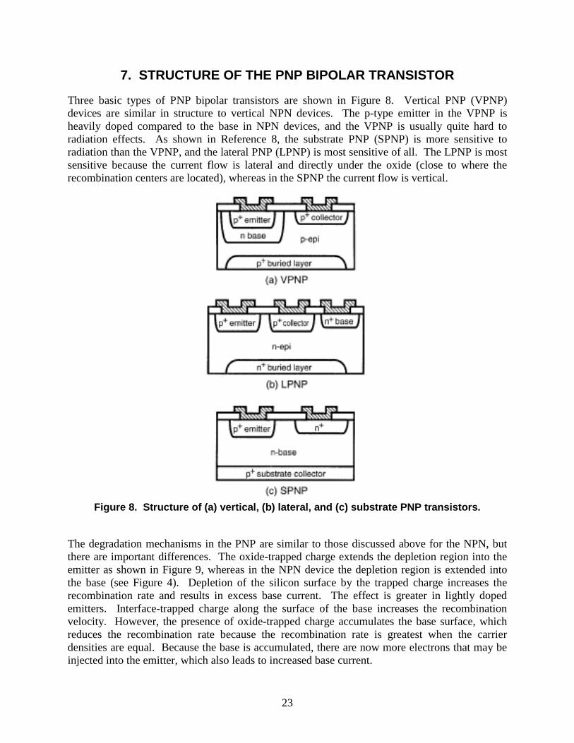
The degradation mechanisms in the PNP are similar to those discussed above for the NPN, but there are important differences. The oxide-trapped charge extends the depletion region into the emitter as shown in Figure 9, whereas in the NPN device the depletion region is extended into the base (see Figure 4). Depletion of the silicon surface by the trapped charge increases the recombination rate and results in excess base current. The effect is greater in lightly doped emitters. Interface-trapped charge along the surface of the base increases the recombination velocity. However, the presence of oxide-trapped charge accumulates the base surface, which reduces the recombination rate because the recombination rate is greatest when the carrier densities are equal. Because the base is accumulated, there are now more electrons that may be injected into the emitter, which also leads to increased base current.
24
As shall be seen in Section 10, the curves for excess base current in PNP devices show characteristics similar to NPN devices, so for the present the model already developed for both NPN and PNP will be used to see how well it does with the PNP data. A model for the effects of trapped charge in an LPNP device is presented in Reference 11, and this or a similar model may need to be included later.
Figure 9. Expansion of depletion region into the emitter from oxide-trapped charge in a
PNP device.
25
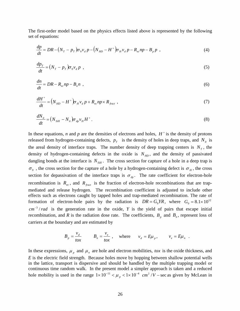
8. MODEL FOR DOSE RATE SENSITIVITY OF TRAPPED CHARGE
When a bipolar device is exposed to ionizing radiation, electron-hole pairs are formed uniformly throughout the base oxide. Holes migrate under the weak fringing field of the emitter-base junction and fields because of any charge trapped in the oxide. Shallow trap sites in the bulk of the oxide can reduce the mobility of the holes as they are trapped and then re-emitted. Holes will also be caught in deep traps in the strained region of the oxide near the silicon interface.
During transport, holes can be captured by hydrogen-containing defects that then release +H in the reaction ,' ++ +→+ HDDHp where DH is the hydrogen-containing defect, D' is the defect with a captured hole, and +H is a proton. With a positive field in the oxide, the +H drifts to the
2/ SiOSi interface, where it reacts with SiH trap precursors to produce unpassivated dangling bonds (interface traps). The reaction creating interface traps can be written
2HSiHSiH +→+ ++ , where SiH is a hydrogen passivated dangling bond in the Si, and +Si is the interface trap. This two-stage model of interface trap buildup is called the hole trapping/hydrogen transport model 2)(HT [12]. Experiments have shown that under a positive field nearly all the +H produced in the oxide is ultimately converted to interface traps [13] [14].
A large number of mechanisms have been identified as contributing to the dose-rate effect in BJTs, probably between 10 and 20. Each of these mechanisms is plausible and probably contributes in various degrees depending on the device structure, fabrication process, and other conditions. A comprehensive review of these mechanisms is given in Reference 5. The mechanisms are grouped into three main categories: (1) space charge models, (2) bimolecular process models, and (3) a binary reaction rate model.
For the purposes here it will not be practical to combine many different dose rate mechanisms in a single model. Instead a few basic processes will be adopted in a first-order (or first-level) model that should apply generally, and additional mechanisms added as required to match the data from different devices. The first-order model includes seven basic processes as follows: (1) hole capture in deep traps near the interface, (2) electron-hole recombination, (3) hydrogen release from capture of transporting holes by hydrogen-containing defects, (4) hydrogen release from trap-mediated recombination involving hydrogen-containing defects, (5) dispersive hole transport, (6) space charge effects from transporting carriers and protons in the oxide, and (7) hydrogen reactions at the interface that produce interface traps.
The principal dose-rate effect in this model results from the competition between hole trapping and electron-hole recombination. This produces a dose-rate effect because the rate of hole trapping depends on the number density of carriers to the first power, and recombination depends on carrier density squared, since both types of carrier are involved. At low dose rates where carrier densities are low, recombination plays less of a role, and at high dose rates where carrier densities are high, recombination dominates. When recombination dominates, holes are removed from the process, resulting in less oxide-trapped charge and less hydrogen release. It is also important to note that recombination is more important when electric fields are low, which is the case in bipolar devices compared to MOSFETs. In a high field situation, the mobile electrons are swept out of the oxide before they can have a significant effect in trapping and recombination.
26
The first-order model based on the physics effects listed above is represented by the following set of equations:
( ) ( ) pBnpRpvHNpvpNDRdtdp
pecdHHDdTT −−−−−−= + σσ 0 , (4)
( ) pvpNdt
dpdTT
T0σ−= , (5)
nBnpRDRdtdn
nec −−= , (6)
( ) fractecdHHD RnpRpvHNdt
dH×+−= +
+
σ , (7)
( ) +−= HvNNdt
dNHdpitSiH
it σ . (8)
In these equations, n and p are the densities of electrons and holes, +H is the density of protons released from hydrogen-containing defects, Tp is the density of holes in deep traps, and itN is the areal density of interface traps. The number density of deep trapping centers is TN , the density of hydrogen-containing defects in the oxide is HDN , and the density of passivated dangling bonds at the interface is SiHN . The cross section for capture of a hole in a deep trap is
0σ , the cross section for the capture of a hole by a hydrogen-containing defect is Hσ , the cross section for depassivation of the interface traps is dpσ . The rate coefficient for electron-hole recombination is ecR , and fractR is the fraction of electron-hole recombinations that are trap-mediated and release hydrogen. The recombination coefficient is adjusted to include other effects such as electrons caught by tapped holes and trap-mediated recombination. The rate of formation of electron-hole pairs by the radiation is YRGDR 0= , where 12
0 101.8 ×=G radcm /3− is the generation rate in the oxide, Y is the yield of pairs that escape initial
recombination, and R is the radiation dose rate. The coefficients, pB and nB , represent loss of carriers at the boundary and are estimated by
toxv
B dp =
toxv
B en = , where pd Ev µ= , ne Ev µ= .
In these expressions, pµ and nµ are hole and electron mobilities, tox is the oxide thickness, and E is the electric field strength. Because holes move by hopping between shallow potential wells in the lattice, transport is dispersive and should be handled by the multiple trapping model or continuous time random walk. In the present model a simpler approach is taken and a reduced hole mobility is used in the range 411 101101 −− ×<<× pµ sec/2 −Vcm as given by McLean in
27
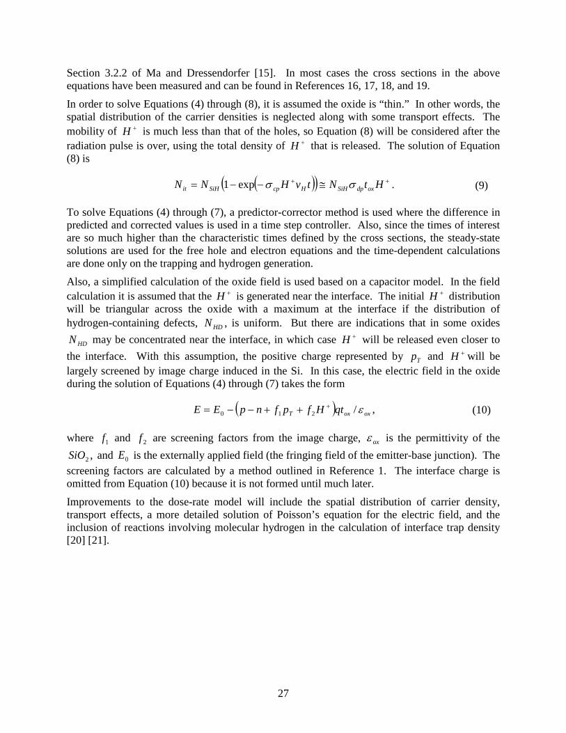
Section 3.2.2 of Ma and Dressendorfer [15]. In most cases the cross sections in the above equations have been measured and can be found in References 16, 17, 18, and 19.
In order to solve Equations (4) through (8), it is assumed the oxide is “thin.” In other words, the spatial distribution of the carrier densities is neglected along with some transport effects. The mobility of +H is much less than that of the holes, so Equation (8) will be considered after the radiation pulse is over, using the total density of +H that is released. The solution of Equation (8) is
( )( ) ++ ≅−−= HtNtvHNN oxdpSiHHcpSiHit σσexp1 . (9)
To solve Equations (4) through (7), a predictor-corrector method is used where the difference in predicted and corrected values is used in a time step controller. Also, since the times of interest are so much higher than the characteristic times defined by the cross sections, the steady-state solutions are used for the free hole and electron equations and the time-dependent calculations are done only on the trapping and hydrogen generation.
Also, a simplified calculation of the oxide field is used based on a capacitor model. In the field calculation it is assumed that the +H is generated near the interface. The initial +H distribution will be triangular across the oxide with a maximum at the interface if the distribution of hydrogen-containing defects, HDN , is uniform. But there are indications that in some oxides
HDN may be concentrated near the interface, in which case +H will be released even closer to the interface. With this assumption, the positive charge represented by Tp and +H will be largely screened by image charge induced in the Si. In this case, the electric field in the oxide during the solution of Equations (4) through (7) takes the form
( ) oxoxT qtHfpfnpEE ε/210+++−−= , (10)
where 1f and 2f are screening factors from the image charge, oxε is the permittivity of the ,2SiO and 0E is the externally applied field (the fringing field of the emitter-base junction). The
screening factors are calculated by a method outlined in Reference 1. The interface charge is omitted from Equation (10) because it is not formed until much later.
Improvements to the dose-rate model will include the spatial distribution of carrier density, transport effects, a more detailed solution of Poisson’s equation for the electric field, and the inclusion of reactions involving molecular hydrogen in the calculation of interface trap density [20] [21].

28

29
9. COMPARING SIMULATION WITH MEASUREMENTS FOR THE 2N2222 AND 2N2907
Figure 10 shows the dose-rate effect in two devices of interest at Sandia National Laboratories (SNL): the 2N2222, which is NPN, and the 2N2907, which is PNP [22]. The degradation plotted is BB II /∆ . These curves show the S-shape typical of the ELDRS effect, namely a saturation at low dose rate that occurs when recombination moves below the surface as in Figure 3, and a flattening at high dose rate. The saturation at high dose rate in the present model is caused by hydrogen release by trap-mediated recombination involving hydrogen-containing defects. At very high dose rates, recombination is high, and because a few percent of recombinations, fractR , release hydrogen by this process, there is a leveling of the dose-rate effect.
Figure 10. Measurement and simulation of the dose-rate effect in 2N2222 and 2N2907 at VBE = 0.5 V.
Red diamonds indicate the simulation.
The simulation points shown in the figures were obtained from Equations (1) through (3) running in Verilog-A under SmartSpice with a numerical solution of Equations (4) through (10) to obtain the trapped charge. The code is given in the Appendices. The parameters used in the simulations are listed in Table 1.
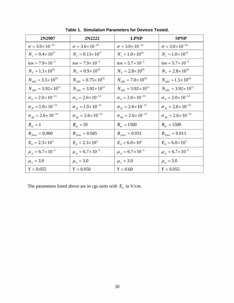
30
Table 1. Simulation Parameters for Devices Tested.
2N2907 2N2222 LPNP SPNP 16100.3 −×=σ 16106.3 −×=σ 16100.3 −×=σ 16100.3 −×=σ 17104.0 ×=sN 171013.0 ×=sN 16100.1 ×=sN 16100.1 ×=sN
5109.7 −×=tox 5109.7 −×=tox 5107.5 −×=tox 5107.5 −×=tox 16101.1 ×=TN 16109.0 ×=TN 16108.2 ×=TN 16108.2 ×=TN
16105.3 ×=HDN 161075.0 ×=HDN 16100.7 ×=HDN 16105.1 ×=HDN 121092.3 ×=SiHN 121092.3 ×=SiHN 121092.3 ×=SiHN 121092.3 ×=SiHN
130 100.2 −×=σ 13
0 100.2 −×=σ 130 100.2 −×=σ 13
0 100.2 −×=σ 13100.1 −×=Hσ 13100.1 −×=Hσ 13106.2 −×=Hσ 13106.2 −×=Hσ 13106.2 −×=dpσ 13106.2 −×=dpσ 13106.2 −×=dpσ 13106.2 −×=dpσ
1=ecR 10=ecR 1500=ecR 1500=ecR
060.0=fractR 045.0=fractR 031.0=fractR 013.0=fractR 3
0 103.2 ×=E 30 103.2 ×=E 3
0 100.6 ×=E 30 100.6 ×=E
5107.6 −×=pµ 5107.6 −×=pµ 5107.6 −×=pµ 5107.6 −×=pµ
0.3=nµ 0.3=nµ 0.3=nµ 0.3=nµ
055.0=Y 050.0=Y 60.0=Y 055.0=Y
The parameters listed above are in cgs units with 0E in V/cm.

31
10. MEASUREMENT AND SIMULATION FOR LATERAL AND SUBSTRATE PNPS
In Reference 23 the dose rate sensitivity of lateral and substrate PNP transistors is investigated experimentally. This section shall attempt to reproduce those measurements with the model developed in Sections 5 and 6. The devices studied in Reference 23 use poly-crystalline emitter technology and have emitter areas of 1.2 mµ × 1.2 mµ . The active base width for the lateral device is 2.6 mµ and for the substrate device is 1.2 mµ . The Doping density at the surface of the base is 316100.1 −× cm , and the oxide thickness is 570 nm. Irradiations involved dose rates between 0.001 and 294 rad(Si)/sec.
The dose-rate effect on excess base current at 20 Krad for both devices is shown in Figures 11 and 12 along with simulation results. The parameters used in the simulations are shown in Table 1.
Figure 11. Measurement and simulation of the dose-rate effect in two PNP devices
at VBE = 0.7 V. Red diamonds indicate the simulation.
32
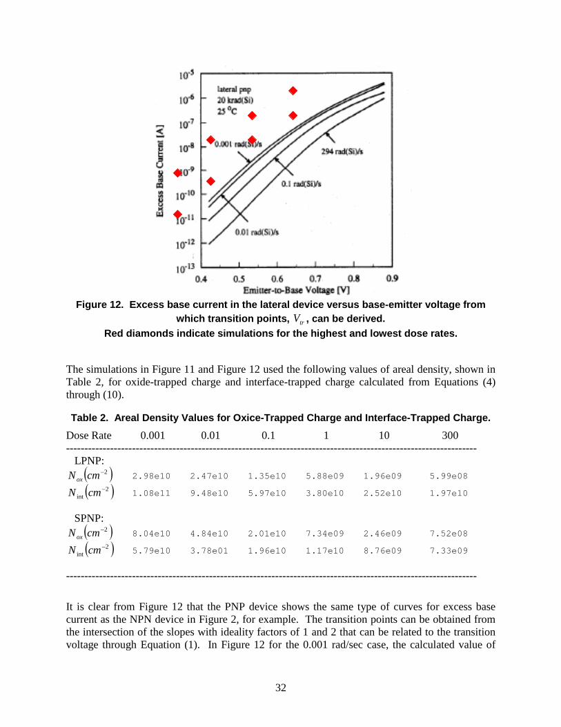
Figure 12. Excess base current in the lateral device versus base-emitter voltage from
which transition points, trV , can be derived. Red diamonds indicate simulations for the highest and lowest dose rates.
The simulations in Figure 11 and Figure 12 used the following values of areal density, shown in Table 2, for oxide-trapped charge and interface-trapped charge calculated from Equations (4) through (10).
Table 2. Areal Density Values for Oxice-Trapped Charge and Interface-Trapped Charge.
Dose Rate 0.001 0.01 0.1 1 10 300 ---------------------------------------------------------------------------------------------------------------- LPNP:
( )2−cmNox 2.98e10 2.47e10 1.35e10 5.88e09 1.96e09 5.99e08
( )2int
−cmN 1.08e11 9.48e10 5.97e10 3.80e10 2.52e10 1.97e10
SPNP:
( )2−cmNox 8.04e10 4.84e10 2.01e10 7.34e09 2.46e09 7.52e08
( )2int
−cmN 5.79e10 3.78e01 1.96e10 1.17e10 8.76e09 7.33e09
----------------------------------------------------------------------------------------------------------------
It is clear from Figure 12 that the PNP device shows the same type of curves for excess base current as the NPN device in Figure 2, for example. The transition points can be obtained from the intersection of the slopes with ideality factors of 1 and 2 that can be related to the transition voltage through Equation (1). In Figure 12 for the 0.001 rad/sec case, the calculated value of

33
oxN given in Table 2 corresponds to a transition voltage 702.0=trV . An inspection of the figure indicates a value of about 69.0=trV .
It is evident from these simulations that the model developed for NPN devices also does a reasonable job of representing the data for PNP devices despite some differences in the physics between the two types of devices.

34

35
11. SUMMARY AND CONCLUSIONS
The objective of this work is to develop a model for total dose effects in BJTs for use in circuit simulation. Total dose effects from radiation exposure are caused by trapped charge in the oxide of the device: the gate oxide in MOSFETs and the base oxide in BJTs. In BJTs the trapped charge causes excess base current from recombination, thereby lowering the gain. A significant complicating factor in BJTs is ELDRS.
If a device that exhibits dose rate sensitivity is exposed to the same total dose at low dose rate or at high dose rate, the radiation damage is much greater in the low dose rate case. The ELDRS situation presents special problems, because it is difficult to do low dose rate experiments in the laboratory because of the long times required. Two situations where ELDRS is a factor are (1) spacecraft missions of long duration through radiation belts and (2) nuclear weapons in storage for many years, the InRad environment.
The model for total dose effects described here has two components. The first is an electrical model of device performance that includes the effects of trapped charge on device behavior, and the second is a model that calculates the trapped charge densities in a specific device structure as a function of radiation dose and dose rate. SNL has developed device models in Verilog-A, including the effects of trapped charge, for four bipolar devices: MMBT2907, MMBT2222, a generic LPNP device and a generic SPNP device. These models require the densities of oxide-trapped charge and interface-trapped charge as input parameters in addition to the usual device parameters for circuit simulation. These devices were chosen for study because measurements that exhibit ELDRS are available in the literature.
A vast amount of work has been done on ELDRS, with well over 100 papers listed in recent surveys of the literature. Most of these studies are academic in nature, focusing on just a few of the possible physics mechanisms involved. Nothing has appeared that presents a comprehensive model capable for use in SPICE-based circuit simulation. This report presents a first-order (or first-level) model for the calculation of trapped charge in BJTs that reproduces well the data reported on the devices listed above.
A large number of physics effects have been identified as contributing to the dose-rate effect in BJTs, probably between 10 and 20. The first-order model presented here includes seven of what are considered to be the most important mechanisms involved in ELDRS. These mechanisms include (1) hole capture in deep traps near the interface, (2) electron-hole recombination, (3) hydrogen release from capture of transporting holes by hydrogen-containing traps, (4) hydrogen release from trap-mediated recombination involving hydrogen-containing defects, (5) dispersive hole transport, (6) space charge effects from transporting carriers and protons in the oxide, and (7) hydrogen reactions at the interface that produce interface traps. The current model is considered a first-level effort because it treats the oxide as “thin.” In other words, the space distribution of carriers in the oxide is neglected along with some transport effects. In addition, a simplified model for the oxide field is used that neglects some of the more complex issues in the oxide field calculation.
36
Future work needs to focus on a more precise treatment of transport and space charge effects (Poisson’s equation), and a number of complex hydrogen reactions that occur in association with interface trap formation need to be included. It may also be necessary to revise the model developed for NPN devices to accommodate the physics differences in PNP devices. On the other hand, the “thin” approximation may be entirely adequate for newer devices built to smaller scale.

37
REFERENCES
1. P. M. Campbell and C. W. Bogdan, Analytical Models for Total Dose Ionization Effects in
MOS Devices, SAND2008-5112. Sandia National Laboratories, Albuquerque, NM, 2008.
2. J. R. Schwank, M. R. Shaneyfelt, D. M. Fleetwood, J. A. Felix, P. E. Dodd, P. Paillet, and V. Ferlet-Cavrois, Radiation Effects in MOS Oxides, IEEE Trans. Nucl. Sci., Vol. 55, pp. 1833-1853, 2008.
3. D. M. Fleetwood, P. S. Winokur, and J. R. Schwank, Using Laboratory X-Ray and Cobalt-60 Irradiations to Predict CMOS Device Response in Strategic and Space Environments, IEEE Trans. Nucl. Sci., Vol. 35, pp. 1497-1505, 1988.
4. R. L. Pease, Total Ionizing Dose Effects in Bipolar Devices and Circuits, IEEE Trans. Nucl. Sci., Vol. 50, pp. 539-551, 2003.
5. R. L. Pease, R. D. Schrimpf, and D. M. Fleetwood, ELDRS in Bipolar Linear Circuits: A Review, IEEE Trans. Nucl. Sci., Vol. 56, pp. 1894-1908, 2009.
6. E. W. Enlow, R. L. Pease, W. Combs, R. D. Schrimpf, and R. N. Nowlin, Response of Advanced Bipolar Processes to Ionizing Radiation, IEEE Trans. Nucl. Sci., Vol. 38, pp. 1342-1351, 1991.
7. S. L. Kosier, R. D. Schrimpf, R. N. Nowlin, D. M. Fleetwood, M. DeLaus, R. L. Pease, W. E. Combs, A. Wei, and F. Chai, Charge Separation for Bipolar Transistors, IEEE Trans. Nucl. Sci., Vol. 40, pp. 1276-1285, 1993.
8. R. D. Schrimpf, Recent Advances in Understanding Total-Dose Effects in Bipolar Transistors, IEEE Trans. Nucl. Sci., Vol. 43, pp. 787-796, 1996.
9. S. L. Kosier, A. Wei, R. D. Schrimpf, D. M. Fleetwood, M. DeLaus, R. L. Pease, and W. E. Combs, Physically Based Comparison of Hot-Carrier-Induced and Ionizing-Radiation-Induced Degradation in BJT’s, IEEE Trans. Nucl. Sci., Vol. 42, pp. 436-443, 1995.
10. W. Shockley and W. T. Read, Jr., Statistics of the Recombination of Holes and Electrons, Phys. Rev., Vol. 87, pp. 835-842, 1952.
11. D. M. Schmidt, A. Wu, R. D. Schrimpf, D. M. Fleetwood, and R. L. Pease, Modeling Ionizing Radiation Induced Gain Degradation of the Lateral PNP Bipolar Junction Transistor, IEEE Trans. Nucl. Sci., Vol. 43, pp. 3032-3039, 1996.
12. M. R. Shaneyfelt, J. R. Schwank, D. M. Fleetwood, P. S. Winokur, K. L. Hughes, G. L. Hash, and M. P. Connors, Interface Trap Buildup in Wet and Dry Oxides, IEEE Trans. Nucl. Sci., Vol. 39, pp. 2244-2251, 1992.
13. B. J. Mrstik and R. W. Rendel, Si-SiO2 Interface State Generation During X-Ray Irradiation and During Post-Irradiation Exposure to Hydrogen Ambient, IEEE Trans. Nucl. Sci., Vol. 38, pp. 1101-1109, 1991.
14. R. E. Stahlbush, A. H. Edwards, D. L. Griscom, and B. J. Mrstik, Post-Irradiation Cracking of H2 and Formation of Interface States in Irradiated MOS Field-Effect Transistors, J. Appl. Phys., Vol. 73, pp. 658-667, 1993.

38
15. T. P. Ma and P. V. Dressendorfer, Ionizing Radiation Effects in MOS Devices and Circuits. Wiley-Interscience, New York, 1989.
16. Tak H. Ning, Capture Cross Section and Trap Concentration of Holes in Silicon Dioxide, J. Appl. Phys., Vol. 47, p. 1079, 1976.
17. S. N. Rashkeev, C. R. Cirba, R. D. Schrimpf, A. Michez, and S. T. Pantelides, Physical Model for Enhanced Interface-Trap Formation at Low Dose Rates, IEEE Trans. Nucl. Sci., Vol. 49, p. 2650, 2002.
18. J. J. Tzou, J. Yuan-Chen Sun, and Chih-Tang Sah, Field Dependence of Two Large Hole Capture Cross Sections in Thermal Oxide on Silicon, Appl. Phys. Lett., Vol. 43, p. 861, 1983.
19. R. Stivers and C. T. Sah, A Study of Oxide Traps and Interface States of the Silicon-Slicon Dioxide Interface, J. Appl. Phys., Vol. 51(12), pp. 6292-6304, 1980.
20. S. N. Rashkeev, D. M. Fleetwood, R. D. Schrimpf, and S. T. Pantelides, Defect Generation by Hydrogen at the Si-SiO2 Interface, Phys. Rev. Lett., Vol. 87, pp. 165506-1–165506-4, 2001.
21. H. P. Hjalmarson, R. L. Pease, S. C. Witczak, M. R. Shaneyfelt, J. R. Schwank, A. H. Edwards, C. E. Hembree, and T. R. Mattsson, Mechanisms for Radiation Dose-Rate Sensitivity of Bipolar Transistors, IEEE Trans. Nucl. Sci., Vol. 50, pp. 1901-1909, 2003.
22. J. Boch, F. Saigne, R. D. Schrimpf, J.-R. Vaille, and L. Dusseau, Physical Model for the Dose-Rate Effect in Bipolar Devices, IEEE Trans. Nucl. Sci., Vol. 53, pp. 3655-3650, 2006.
23. S. C. Witczak, R. D. Schrimpf, K. F. Galloway, D. M Fleetwood, R. L. Pease, J. M. Puhl, D. M. Schmidt, W. E. Combs, and J. S. Suehle, Accelerated Tests for Simulating Low Dose Rate Gain Degradation of Lateral and Substrate PNP Bipolar Junction Transistors, IEEE Trans. Nucl. Sci., Vol. 43, pp. 3151-3160, 1996.
39
APPENDIX A
VERILOG-A MODEL FOR 2N2222 WITH TD EFFECTS
// JAN2N2222 NPN Bipolar Transistor Model with Total Dose Effects // Version 1b August 2, 2011 // P. M. Campbell and D. N. Shirley `include "discipline.h" module JAN2N2222(Coll,Base,Emit); inout Coll,Base,Emit; electrical Coll,Base,Emit,CollP,BaseP,EmitP,gnd; ground gnd; // default parameters for the JAN2N2222 transistor, NPN parameter real Gmin=1.0e-12 from [0:inf); parameter real PTF=0 from [0:inf); parameter real ITF=0 from [0:inf); parameter real VTF=1e3 from [0:inf); parameter real XTF=0 from [0:inf); parameter real XTI=3 from [0:inf); parameter real XTB=0 from [0:inf); parameter real TR=0 from [0:inf); parameter real TF=0 from [0:inf); parameter real FC=0.5 from [0:inf); parameter real XCJC=1.0 from [0:inf); parameter real MJS=0 from [0:inf); parameter real VJS=0.75 from [0:inf); parameter real CJS=0 from [0:inf); parameter real MJC=0.2796 from [0:inf); parameter real VJC=0.5086 from [0:inf); parameter real CJC=1.088e-11 from [0:inf); parameter real MJE=0.3132 from [0:inf); parameter real VJE=0.6879 from [0:inf); parameter real CJE=26.63e-12 from [0:inf); parameter real eg=1.11 from [0:inf); parameter real re=0.1 from [0:inf); parameter real rc=1.271 from [0:inf); // parameter real rb=28.97 from [0:inf); parameter real rb=7.1 from [0:inf); parameter real rbm=0.001 from [0:inf); parameter real irb=0.00145 from [0:inf); parameter real IKR=0.1065 from [0:inf);

40
parameter real nc=1.391 from [0:inf); parameter real ISC=1.015e-13 from [0:inf); parameter real nr=0.9813 from [0:inf); parameter real br=11.82 from [0:inf); parameter real Var=15.46 from (0:inf]; parameter real Vaf=1e99 from (0:inf]; parameter real nk=1.3 from [0:inf); parameter real IKF=1.0 from [0:inf); parameter real ne=1.44 from (0:inf); parameter real ISE=4.589e-15 from (0:inf); parameter real nf=0.9749 from (0:inf); parameter real bf=150.0 from [0:inf); parameter real IS=1.065e-14 from (0:inf); parameter real sigma=3.6e-16; parameter real q=1.6e-19; parameter real ni=1e+10; parameter real vth=1.17e+7; parameter real eps=11.9; parameter real taub=1e-8; // note there is no area parameter here yet real Vbe, Vbc, Vbx, Vcs, VBGmin, VCGmin; real vtF, vtR, vtE, vtC; real nk0, q0, q1, q2, qb, arg; real fe1, fe2, fe3, fc1, fc2, fc3; real Ic, Ib, fcvje, fcvjc, arg1, arg2; real Qbe, Qbc, Qbx, Qcs, Qbed, Qbcd; real deltIB_inv1, deltIB_inv2; real deltIB, deltIB0, deltIB1, deltIB2, deltIB3; real Dose, Nox, NT, Ns, Ld, Pe, deltaL, LIB; real x, deltax1, vsurf, T, Vtran; analog begin @(initial_step) begin fe1 = (VJE/(1-MJE))*(1 - pow((1-FC), 1-MJE)); fe2 = pow((1-FC), (1+MJE)); fe3 = 1 - FC*(1+MJE); fcvje = FC*VJE; fc1 = (VJC/(1-MJC))*(1 - pow((1-FC), 1-MJC)); fc2 = pow((1-FC), (1+MJC)); fc3 = 1 - FC*(1+MJC);

41
fcvjc = FC*VJC; vtF = nf*$vt; vtR = nr*$vt; vtE = ne*$vt; vtC = nc*$vt; if(nk == 0) nk0 = 0.5; else nk0 = nk; // Radiation effects Dose = 0; Nox = 0; NT = 0; // Dose = 20; // Nox = 7.3e10; // NT = 3.3e10; // Nox = 6.6e10; // NT = 3.0e10; // Nox = 5.4e10; // NT = 2.4e10; // Nox = 5.6e10; // NT = 2.5e10; // Nox = 5.6e10; // NT = 2.5e10; // Dose = 30; // Nox = 1.0e11; // NT = 4.6e10; // Nox = 9.9e10; // NT = 4.5e10; // Nox = 8.0e10; // NT = 3.6e10; // Nox = 8.1e10; // NT = 3.7e10; // Nox = 8.1e10; // NT = 3.7e10; // new values for charge // Nox = 1.0e11; // NT = 4.7e10; // Nox = 1.0e11; // NT = 4.6e10; // Nox = 9.3e10; // NT = 4.0e10; // Nox = 7.8e10; // NT = 3.4e10;
42
// Nox = 5.7e10; // NT = 2.5e10; // Device structure for JAN2N2222 Pe = 0.267; // LIB = 12.3e-4; LIB = 10.3e-4; deltaL = 1e-4; // Ns = 1.0e17; Ns = 0.13e17; T = 300; Ld = 743.9*sqrt($vt*eps/Ns); x = Nox/(sqrt(2)*Ld*Ns); vsurf = sigma*vth*NT; Vtran = $vt*2*ln(Ns/ni) - q*Nox*Nox/(eps*8.854e-14*Ns); if(Vtran < 0) Vtran = 0.1; // First calculate deltax from transition point if(Dose == 0) begin deltIB0 = 0; deltax1 = 0; end else begin deltIB0 = 0.5*q*ni; deltIB1 = deltIB0*vsurf*Pe*deltaL*exp(0.5*Vtran/$vt); deltIB2 = deltIB0*vsurf*Pe*LIB*2*(ni/Ns)*(1+4*LIB/Pe)*exp(x*x)*exp(Vtran/$vt); deltIB3 = deltIB0*(4/taub)*LIB*LIB*(1+0.25*Pe/LIB)*exp(0.5*Vtran/$vt); deltax1 = (deltIB1 + deltIB2)/deltIB3; $debug ("Ns = %g, Nox = %g, NT = %g, Vtran = %g", Ns,Nox,NT,Vtran); $debug ("Ld = %g, deltax1 = %g, vsurf = %g", Ld,deltax1,vsurf); end end // $debug ("time = %g", $abstime); // Internal voltage drops V(Coll,CollP) <+ rc*I(Coll); V(Base,BaseP) <+ rb*I(Base); V(Emit,EmitP) <+ re*I(Emit); Vbe = V(BaseP) - V(EmitP); Vbc = V(BaseP) - V(CollP); Vbx = V(Base) - V(CollP); Vcs = V(CollP) - V(gnd);

43
// High current rolloff q0 = (Vbe/IKF+Vbc/IKR)*Gmin; q1 = 1/(1 - Vbc/Vaf - Vbe/Var); if((Vbe > -5*vtF) && (Vbc <= -5*vtR)) begin q2 = (IS/IKF)*(exp(Vbe/vtF)-1) - IS/IKR + q0; $debug ("Vb = %g, first q2 = %g", V(Base),q2); end else if((Vbe <= -5*vtF) && (Vbc > -5*vtR)) begin q2 = (IS/IKR)*(exp(Vbc/vtR)-1) - IS/IKF + q0; $debug ("Vb = %g, second q2 = %g", V(Base),q2); end else if((Vbe > -5*vtF) && (Vbc > -5*vtR)) begin q2 = (IS/IKF)*(exp(Vbe/vtF)-1) + (IS/IKR)*(exp(Vbc/vtR)-1) + q0; $debug ("Vb = %g, third q2 = %g", V(Base),q2); end else if((Vbe <= -5*vtF) && (Vbc <= -5*vtR)) begin q2 = -IS*(IKF+IKR)/(IKF*IKR) + q0; $debug ("Vb = %g, fourth q2 = %g", V(Base),q2); end arg = 1+4*q2; if(arg > 0) qb = 0.5*q1*(1 + pow(arg,nk0)); else qb = q1; $debug ("qb = %g", qb); // SPICE2 BJT, Gummel-Poon Model VBGmin = (Vbe/bf+Vbc/br)*Gmin; VCGmin = ((Vbe-Vbc)/qb - Vbc/br)*Gmin; if((Vbe > -5*vtF) && (Vbc <= -5*vtR)) begin Ic = (IS/qb)*(exp(Vbe/vtF)+qb/br) + ISC + VCGmin; Ib = IS*((exp(Vbe/vtF)-1)/bf-1/br) + ISE*(exp(Vbe/vtE)-1) - ISC + VBGmin; end else if((Vbe <= -5*vtF) && (Vbc > -5*vtR)) begin Ic = -(IS/qb)*(exp(Vbc/vtR)+(qb/br)*(exp(Vbc/vtR)-1)) -ISC*(exp(Vbc/vtC)-1) + VCGmin;
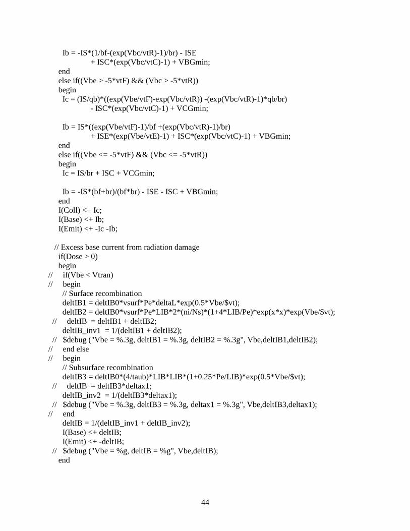
44
Ib = -IS*(1/bf-(exp(Vbc/vtR)-1)/br) - ISE + ISC*(exp(Vbc/vtC)-1) + VBGmin; end else if((Vbe > -5*vtF) && (Vbc > -5*vtR)) begin Ic = (IS/qb)*((exp(Vbe/vtF)-exp(Vbc/vtR)) -(exp(Vbc/vtR)-1)*qb/br) - ISC*(exp(Vbc/vtC)-1) + VCGmin; Ib = IS*((exp(Vbe/vtF)-1)/bf +(exp(Vbc/vtR)-1)/br) + ISE*(exp(Vbe/vtE)-1) + ISC*(exp(Vbc/vtC)-1) + VBGmin; end else if((Vbe <= -5*vtF) && (Vbc <= -5*vtR)) begin Ic = IS/br + ISC + VCGmin; Ib = -IS*(bf+br)/(bf*br) - ISE - ISC + VBGmin; end I(Coll) <+ Ic; I(Base) <+ Ib; I(Emit) <+ -Ic -Ib; // Excess base current from radiation damage if(Dose > 0) begin // if(Vbe < Vtran) // begin // Surface recombination deltIB1 = deltIB0*vsurf*Pe*deltaL*exp(0.5*Vbe/$vt); deltIB2 = deltIB0*vsurf*Pe*LIB*2*(ni/Ns)*(1+4*LIB/Pe)*exp(x*x)*exp(Vbe/$vt); // deltIB = deltIB1 + deltIB2; deltIB_inv1 = 1/(deltIB1 + deltIB2); // $debug ("Vbe = %.3g, deltIB1 = %.3g, deltIB2 = %.3g", Vbe,deltIB1,deltIB2); // end else // begin // Subsurface recombination deltIB3 = deltIB0*(4/taub)*LIB*LIB*(1+0.25*Pe/LIB)*exp(0.5*Vbe/$vt); // deltIB = deltIB3*deltax1; deltIB_inv2 = 1/(deltIB3*deltax1); // $debug ("Vbe = %.3g, deltIB3 = %.3g, deltax1 = %.3g", Vbe,deltIB3,deltax1); // end deltIB = 1/(deltIB_inv1 + deltIB_inv2); I(Base) <+ deltIB; I(Emit) <+ -deltIB; // $debug ("Vbe = %g, deltIB = %g", Vbe,deltIB); end
45
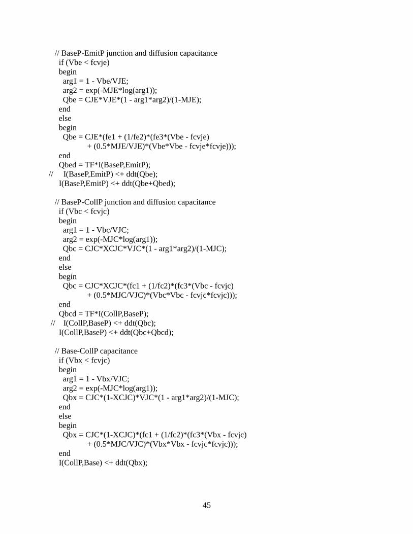
// BaseP-EmitP junction and diffusion capacitance if (Vbe < fcvje) begin arg1 = 1 - Vbe/VJE; arg2 = exp(-MJE*log(arg1)); Qbe = CJE*VJE*(1 - arg1*arg2)/(1-MJE); end else begin Qbe = CJE*(fe1 + (1/fe2)*(fe3*(Vbe - fcvje) + (0.5*MJE/VJE)*(Vbe*Vbe - fcvje*fcvje))); end Qbed = TF*I(BaseP,EmitP); // I(BaseP,EmitP) <+ ddt(Qbe); I(BaseP,EmitP) <+ ddt(Qbe+Qbed); // BaseP-CollP junction and diffusion capacitance if (Vbc < fcvjc) begin arg1 = 1 - Vbc/VJC; arg2 = exp(-MJC*log(arg1)); Qbc = CJC*XCJC*VJC*(1 - arg1*arg2)/(1-MJC); end else begin Qbc = CJC*XCJC*(fc1 + (1/fc2)*(fc3*(Vbc - fcvjc) + (0.5*MJC/VJC)*(Vbc*Vbc - fcvjc*fcvjc))); end Qbcd = TF*I(CollP,BaseP); // I(CollP,BaseP) <+ ddt(Qbc); I(CollP,BaseP) <+ ddt(Qbc+Qbcd); // Base-CollP capacitance if (Vbx < fcvjc) begin arg1 = 1 - Vbx/VJC; arg2 = exp(-MJC*log(arg1)); Qbx = CJC*(1-XCJC)*VJC*(1 - arg1*arg2)/(1-MJC); end else begin Qbx = CJC*(1-XCJC)*(fc1 + (1/fc2)*(fc3*(Vbx - fcvjc) + (0.5*MJC/VJC)*(Vbx*Vbx - fcvjc*fcvjc))); end I(CollP,Base) <+ ddt(Qbx);
46
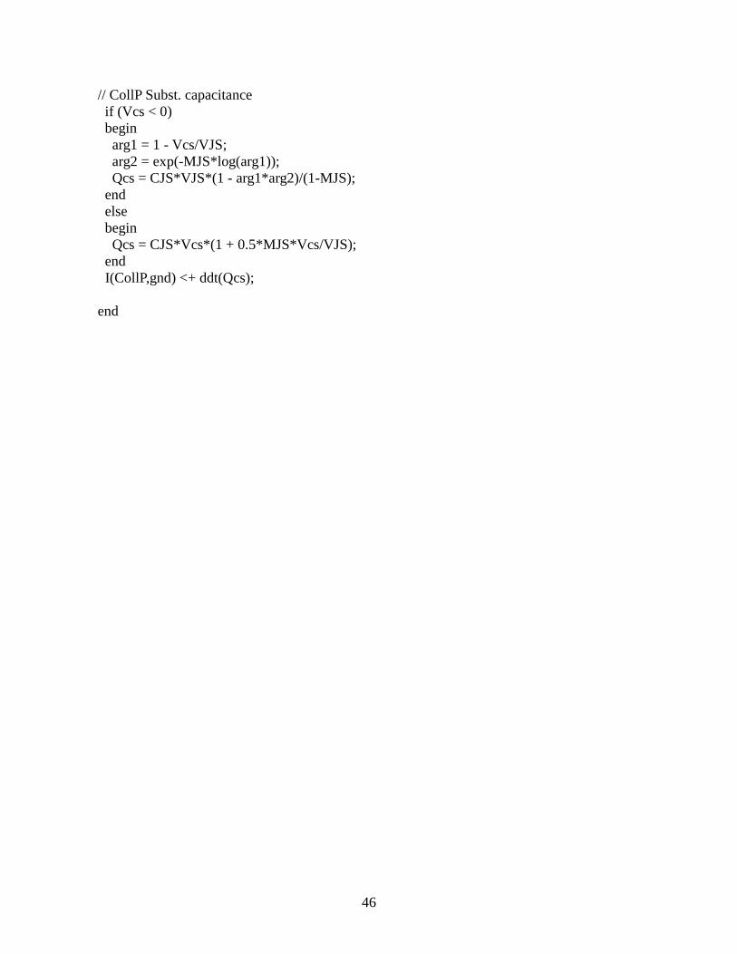
// CollP Subst. capacitance if (Vcs < 0) begin arg1 = 1 - Vcs/VJS; arg2 = exp(-MJS*log(arg1)); Qcs = CJS*VJS*(1 - arg1*arg2)/(1-MJS); end else begin Qcs = CJS*Vcs*(1 + 0.5*MJS*Vcs/VJS); end I(CollP,gnd) <+ ddt(Qcs); end

47
APPENDIX B
VERILOG-A MODEL FOR 2N2907 WITH TD EFFECTS
// JAN2N2907 PNP Bipolar Transistor Model // Version 1b August 4, 2011 // P. M. Campbell and D. N. Shirley `include "discipline.h" module JAN2N2907(Coll,Base,Emit); inout Coll,Base,Emit; electrical Coll,Base,Emit,CollP,BaseP,EmitP,gnd; ground gnd; // default parameters for the JAN2N2907 PNP transistor parameter real Gmin=1.0e-12 from [0:inf); parameter real PTF=0 from [0:inf); parameter real ITF=0 from [0:inf); parameter real VTF=1000 from [0:inf); parameter real XTF=0 from [0:inf); parameter real TR=0 from [0:inf); parameter real TF=0 from [0:inf); parameter real TYPE=-1; parameter real FC=0.5 from [0:inf); parameter real EG=1.11 from [0:inf); parameter real XCJC=1.0 from [0:inf); parameter real XTI=3.0 from [0:inf); parameter real XTB=1.0 from [0:inf); parameter real MJS=0 from [0:inf); parameter real VJS=0.75 from [0:inf); parameter real CJS=0 from [0:inf); parameter real MJC=0.4 from [0:inf); parameter real VJC=0.7 from [0:inf); parameter real CJC=1.00e-12 from [0:inf); parameter real MJE=0.4 from [0:inf); parameter real VJE=0.7 from [0:inf); parameter real CJE=1.00e-12 from [0:inf); parameter real re=0.03108 from [0:inf); parameter real rc=0.6492 from [0:inf); // parameter real rb=21.03 from [0:inf); parameter real rb=4.1 from [0:inf); parameter real rbm=0.001 from [0:inf); parameter real irb=0.0003612 from [0:inf);
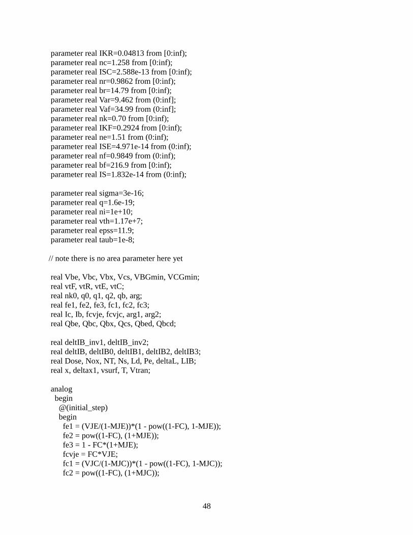
48
parameter real IKR=0.04813 from [0:inf); parameter real nc=1.258 from [0:inf); parameter real ISC=2.588e-13 from [0:inf); parameter real nr=0.9862 from [0:inf); parameter real br=14.79 from [0:inf); parameter real Var=9.462 from (0:inf]; parameter real Vaf=34.99 from (0:inf]; parameter real nk=0.70 from [0:inf); parameter real IKF=0.2924 from [0:inf); parameter real ne=1.51 from (0:inf); parameter real ISE=4.971e-14 from (0:inf); parameter real nf=0.9849 from (0:inf); parameter real bf=216.9 from [0:inf); parameter real IS=1.832e-14 from (0:inf); parameter real sigma=3e-16; parameter real q=1.6e-19; parameter real ni=1e+10; parameter real vth=1.17e+7; parameter real epss=11.9; parameter real taub=1e-8; // note there is no area parameter here yet real Vbe, Vbc, Vbx, Vcs, VBGmin, VCGmin; real vtF, vtR, vtE, vtC; real nk0, q0, q1, q2, qb, arg; real fe1, fe2, fe3, fc1, fc2, fc3; real Ic, Ib, fcvje, fcvjc, arg1, arg2; real Qbe, Qbc, Qbx, Qcs, Qbed, Qbcd; real deltIB_inv1, deltIB_inv2; real deltIB, deltIB0, deltIB1, deltIB2, deltIB3; real Dose, Nox, NT, Ns, Ld, Pe, deltaL, LIB; real x, deltax1, vsurf, T, Vtran; analog begin @(initial_step) begin fe1 = (VJE/(1-MJE))*(1 - pow((1-FC), 1-MJE)); fe2 = pow((1-FC), (1+MJE)); fe3 = 1 - FC*(1+MJE); fcvje = FC*VJE; fc1 = (VJC/(1-MJC))*(1 - pow((1-FC), 1-MJC)); fc2 = pow((1-FC), (1+MJC));

49
fc3 = 1 - FC*(1+MJC); fcvjc = FC*VJC; vtF = nf*$vt; vtR = nr*$vt; vtE = ne*$vt; vtC = nc*$vt; if(nk == 0) nk0 = 0.5; else nk0 = nk; // Radiation effects Dose = 0; Nox = 0; NT = 0; // Dose = 20; // Nox = 9.2e10; // NT = 1.3e11; // Nox = 9.9e10; // NT = 1.4e11; // Nox = 9.2e10; // NT = 1.3e11; // Nox = 7.0e10; // NT = 9.8e10; // Nox = 3.8e10; // NT = 5.2e10; // Nox = 3.6e10; // NT = 5.0e10; // Dose = 30; // Nox = 1.37e11; // NT = 2.0e11; // Nox = 1.48e11; // NT = 2.1e11; // Nox = 1.4e11; // NT = 2.1e11; // Nox = 1.0e11; // NT = 1.5e11; // Nox = 5.7e10; // NT = 7.9e10; // Nox = 5.8e10; // NT = 8.0e10; // Device structure for JAN2N2907 Pe = 0.264; // LIB = 10.6e-4; LIB = 12.6e-4;
50
deltaL = 1e-4; // Ns = 1.0e17; Ns = 0.4e17; T = 300; Ld = 743.9*sqrt($vt*epss/Ns); x = Nox/(sqrt(2)*Ld*Ns); vsurf = sigma*vth*NT; Vtran = $vt*2*ln(Ns/ni) - q*Nox*Nox/(epss*8.854e-14*Ns); if(Vtran < 0) Vtran = 0.1; // First calculate deltax from transition point if(Dose == 0) begin deltIB0 = 0; deltax1 = 0; end else begin deltIB0 = 0.5*q*ni; deltIB1 = deltIB0*vsurf*Pe*deltaL*exp(0.5*Vtran/$vt); deltIB2 = deltIB0*vsurf*Pe*LIB*2*(ni/Ns)*(1+4*LIB/Pe)*exp(x*x)*exp(Vtran/$vt); deltIB3 = deltIB0*(4/taub)*LIB*LIB*(1+0.25*Pe/LIB)*exp(0.5*Vtran/$vt); deltax1 = (deltIB1 + deltIB2)/deltIB3; $debug ("Ns = %g, Nox = %g, NT = %g, Vtran = %g", Ns,Nox,NT,Vtran); $debug ("Ld = %g, deltax1 = %g, vsurf = %g", Ld,deltax1,vsurf); end end // $debug ("time = %g", $abstime); // Internal voltage drops V(Coll,CollP) <+ rc*I(Coll); V(Base,BaseP) <+ rb*I(Base); V(Emit,EmitP) <+ re*I(Emit); Vbe = TYPE*(V(BaseP) - V(EmitP)); Vbc = TYPE*(V(BaseP) - V(CollP)); Vbx = TYPE*(V(Base) - V(CollP)); Vcs = TYPE*(V(CollP) - V(gnd)); // High current rolloff q0 = (Vbe/IKF+Vbc/IKR)*Gmin; q1 = 1/(1 - Vbc/Vaf - Vbe/Var); if((Vbe > -5*vtF) && (Vbc <= -5*vtR)) q2 = (IS/IKF)*(exp(Vbe/vtF)-1) - IS/IKR + q0; else if((Vbe <= -5*vtF) && (Vbc > -5*vtR)) q2 = (IS/IKR)*(exp(Vbc/vtR)-1) - IS/IKF + q0;
51
else if((Vbe > -5*vtF) && (Vbc > -5*vtR)) q2 = (IS/IKF)*(exp(Vbe/vtF)-1) + (IS/IKR)*(exp(Vbc/vtR)-1) + q0; else if((Vbe <= -5*vtF) && (Vbc <= -5*vtR)) q2 = -IS*(IKF+IKR)/(IKF*IKR) + q0; arg = 1+4*q2; if(arg > 0) qb = 0.5*q1*(1 + pow(arg,nk0)); else qb = q1; // SPICE2 BJT, Gummel-Poon Model VBGmin = (Vbe/bf+Vbc/br)*Gmin; VCGmin = ((Vbe-Vbc)/qb - Vbc/br)*Gmin; if((Vbe > -5*vtF) && (Vbc <= -5*vtR)) begin Ic = (IS/qb)*(exp(Vbe/vtF)+qb/br) + ISC + VCGmin; Ib = IS*((exp(Vbe/vtF)-1)/bf-1/br) + ISE*(exp(Vbe/vtE)-1) - ISC + VBGmin; end else if((Vbe <= -5*vtF) && (Vbc > -5*vtR)) begin Ic = -(IS/qb)*(exp(Vbc/vtR)+(qb/br)*(exp(Vbc/vtR)-1)) -ISC*(exp(Vbc/vtC)-1) + VCGmin; Ib = -IS*(1/bf-(exp(Vbc/vtR)-1)/br) - ISE + ISC*(exp(Vbc/vtC)-1) + VBGmin; end else if((Vbe > -5*vtF) && (Vbc > -5*vtR)) begin Ic = (IS/qb)*((exp(Vbe/vtF)-exp(Vbc/vtR)) -(exp(Vbc/vtR)-1)*qb/br) - ISC*(exp(Vbc/vtC)-1) + VCGmin; Ib = IS*((exp(Vbe/vtF)-1)/bf +(exp(Vbc/vtR)-1)/br) + ISE*(exp(Vbe/vtE)-1) + ISC*(exp(Vbc/vtC)-1) + VBGmin; end else if((Vbe <= -5*vtF) && (Vbc <= -5*vtR)) begin Ic = IS/br + ISC + VCGmin; Ib = -IS*(bf+br)/(bf*br) - ISE - ISC + VBGmin; end I(Coll) <+ TYPE*Ic; I(Base) <+ TYPE*Ib; I(Emit) <+ TYPE*(-Ic -Ib);
52
// Excess base current from radiation damage if(Dose > 0) begin // if(Vbe < Vtran) // begin // Surface recombination deltIB1 = deltIB0*vsurf*Pe*deltaL*exp(0.5*Vbe/$vt); deltIB2 = deltIB0*vsurf*Pe*LIB*2*(ni/Ns)*(1+4*LIB/Pe)*exp(x*x)*exp(Vbe/$vt); // deltIB = deltIB1 + deltIB2; deltIB_inv1 = 1/(deltIB1 + deltIB2); // $debug ("Vbe = %g, deltIB1 = %g, deltIB2 = %g", Vbe,deltIB1,deltIB2); // end else // begin // Subsurface recombination deltIB3 = deltIB0*(4/taub)*LIB*LIB*(1+0.25*Pe/LIB)*exp(0.5*Vbe/$vt); // deltIB = deltIB3*deltax1; deltIB_inv2 = 1/(deltIB3*deltax1); // $debug ("Vbe = %g, deltIB3 = %g, deltax1 = %g", Vbe,deltIB3,deltax1); // end deltIB = 1/(deltIB_inv1 + deltIB_inv2); I(Base) <+ TYPE*deltIB; I(Emit) <+ -TYPE*deltIB; end // BaseP-EmitP junction and diffusion capacitance if (Vbe < fcvje) begin arg1 = 1 - Vbe/VJE; arg2 = exp(-MJE*log(arg1)); Qbe = CJE*VJE*(1 - arg1*arg2)/(1-MJE); end else begin Qbe = CJE*(fe1 + (1/fe2)*(fe3*(Vbe - fcvje) + (0.5*MJE/VJE)*(Vbe*Vbe - fcvje*fcvje))); end Qbed = TF*I(BaseP,EmitP); // I(BaseP,EmitP) <+ TYPE*ddt(Qbe); I(BaseP,EmitP) <+ TYPE*ddt(Qbe+Qbed); // BaseP-CollP junction and diffusion capacitance if (Vbc < fcvjc) begin arg1 = 1 - Vbc/VJC; arg2 = exp(-MJC*log(arg1));
53
Qbc = CJC*XCJC*VJC*(1 - arg1*arg2)/(1-MJC); end else begin Qbc = CJC*XCJC*(fc1 + (1/fc2)*(fc3*(Vbc - fcvjc) + (0.5*MJC/VJC)*(Vbc*Vbc - fcvjc*fcvjc))); end Qbcd = TF*I(CollP,BaseP); // I(CollP,BaseP) <+ TYPE*ddt(Qbc); I(CollP,BaseP) <+ TYPE*ddt(Qbc+Qbcd); // Base-CollP capacitance if (Vbx < fcvjc) begin arg1 = 1 - Vbx/VJC; arg2 = exp(-MJC*log(arg1)); Qbx = CJC*(1-XCJC)*VJC*(1 - arg1*arg2)/(1-MJC); end else begin Qbx = CJC*(1-XCJC)*(fc1 + (1/fc2)*(fc3*(Vbx - fcvjc) + (0.5*MJC/VJC)*(Vbx*Vbx - fcvjc*fcvjc))); end I(CollP,Base) <+ TYPE*ddt(Qbx); // CollP Subst. capacitance if (Vcs < 0) begin arg1 = 1 - Vcs/VJS; arg2 = exp(-MJS*log(arg1)); Qcs = CJS*VJS*(1 - arg1*arg2)/(1-MJS); end else begin Qcs = CJS*Vcs*(1 + 0.5*MJS*Vcs/VJS); end I(CollP,gnd) <+ TYPE*ddt(Qcs); End

54
55
APPENDIX C
VERILOG-A MODEL FOR LPNP AND SPNP DEVICES WITH TD EFFECTS
// Bipolar Transistor Model for LPNP and SPNP // Version 1b August 4, 2011 // Fits data from Witczak, et al. (1996) // P. M. Campbell and D. N. Shirley `include "discipline.h" module LPNP(Coll,Base,Emit); //module SPNP(Coll,Base,Emit); inout Coll,Base,Emit; electrical Coll,Base,Emit,CollP,BaseP,EmitP,gnd; ground gnd; // default parameters parameter real Gmin=1.0e-12 from [0:inf); parameter real PTF=0 from [0:inf); parameter real ITF=0 from [0:inf); parameter real VTF=1e99 from [0:inf); parameter real XTF=0 from [0:inf); parameter real TR=0 from [0:inf); parameter real TF=0 from [0:inf); parameter real FC=0.5 from [0:inf); parameter real XCJC=1.0 from [0:inf); parameter real MJS=0 from [0:inf); parameter real VJS=0.75 from [0:inf); parameter real CJS=0 from [0:inf); parameter real MJC=0.33 from [0:inf); parameter real VJC=0.75 from [0:inf); parameter real CJC=11.8377e-12 from [0:inf); parameter real MJE=0.33 from [0:inf); parameter real VJE=0.75 from [0:inf); parameter real CJE=36.2005e-12 from [0:inf); parameter real re=0.0 from [0:inf); parameter real rc=0.5 from [0:inf); parameter real rb=5.5 from [0:inf); parameter real IKR=1e99 from [0:inf); parameter real nc=2 from [0:inf); parameter real ISC=0 from [0:inf); parameter real nr=1 from [0:inf);

56
parameter real br=1 from [0:inf); parameter real Var=100 from (0:inf]; parameter real Vaf=100 from (0:inf]; parameter real nk=1.74 from [0:inf); parameter real IKF=1.12 from [0:inf); parameter real ne=1.230 from (0:inf); parameter real ISE=1.4e-14 from (0:inf); parameter real nf=1.0 from (0:inf); parameter real bf=265 from [0:inf); parameter real IS=7.00e-14 from (0:inf); parameter real sigma=3e-16; parameter real q=1.6e-19; parameter real ni=1e+10; parameter real vth=1.17e+7; parameter real eps=11.9; parameter real taub=1e-8; // note there is no area parameter here yet real Vbe, Vbc, Vbx, Vcs, VBGmin, VCGmin; real vtF, vtR, vtE, vtC; real nk0, q0, q1, q2, qb, arg; real fe1, fe2, fe3, fc1, fc2, fc3; real Ic, Ib, fcvje, fcvjc, arg1, arg2; real Qbe, Qbc, Qbx, Qcs, Qbed, Qbcd; real deltIB, deltIB0, deltIB1, deltIB2, deltIB3; real Dose, Nox, NT, Ns, Ld, Pe, deltaL, LIB; real x, deltax1, vsurf, T, Vtran; analog begin @(initial_step) begin fe1 = (VJE/(1-MJE))*(1 - pow((1-FC), 1-MJE)); fe2 = pow((1-FC), (1+MJE)); fe3 = 1 - FC*(1+MJE); fcvje = FC*VJE; fc1 = (VJC/(1-MJC))*(1 - pow((1-FC), 1-MJC)); fc2 = pow((1-FC), (1+MJC)); fc3 = 1 - FC*(1+MJC); fcvjc = FC*VJC; vtF = nf*$vt; vtR = nr*$vt; vtE = ne*$vt;

57
vtC = nc*$vt; if(nk == 0) nk0 = 0.5; else nk0 = nk; // Radiation effects Dose = 0; Nox = 0; NT = 0; // from tdose15x.c // Dose = 20; // Nox = 5.05e10; // NT = 1.30e11; // Nox = 3.63e10; // NT = 9.90e10; // Nox = 1.60e10; // NT = 5.41e10; // Nox = 6.55e09; // NT = 3.65e10; // Nox = 1.94e09; // NT = 2.43e10; // Nox = 5.90e08; // NT = 2.04e10; // Nox = 3.54e08; // NT = 2.06e10; // Device structure for LPNP Pe = 4.8e-4; LIB = 2.6e-4; deltaL = 1e-4; Ns = 1.0e16; // Device structure for SPNP // Pe = 4.8e-4; // LIB = 1.2e-4; // deltaL = 1e-4; // Ns = 1.0e16; T = 300; Ld = 743.9*sqrt($vt*eps/Ns); x = Nox/(sqrt(2)*Ld*Ns); vsurf = sigma*vth*NT; Vtran = $vt*2*ln(Ns/ni) - q*Nox*Nox/(eps*8.854e-14*Ns); if(Vtran < 0) Vtran = 0.1;
58
// First calculate deltax from transition point if(Dose == 0) begin deltIB0 = 0; deltax1 = 0; end else begin deltIB0 = 0.5*q*ni; deltIB1 = deltIB0*vsurf*Pe*deltaL*exp(0.5*Vtran/$vt); deltIB2 = deltIB0*vsurf*Pe*LIB*2*(ni/Ns)*(1+4*LIB/Pe)*exp(x*x)*exp(Vtran/$vt); deltIB3 = deltIB0*(4/taub)*LIB*LIB*(1+0.25*Pe/LIB)*exp(0.5*Vtran/$vt); deltax1 = (deltIB1 + deltIB2)/deltIB3; end $debug ("Ns = %g, Nox = %g, NT = %g, Vtran = %g", Ns,Nox,NT,Vtran); $debug ("Ld = %g, deltax1 = %g, vsurf = %g", Ld,deltax1,vsurf); end // $debug ("time = %g", $abstime); // Internal voltage drops V(Coll,CollP) <+ rc*I(Coll); V(Base,BaseP) <+ rb*I(Base); V(Emit,EmitP) <+ re*I(Emit); Vbe = V(BaseP) - V(EmitP); Vbc = V(BaseP) - V(CollP); Vbx = V(Base) - V(CollP); Vcs = V(CollP) - V(gnd); // High current rolloff q0 = (Vbe/IKF+Vbc/IKR)*Gmin; q1 = 1/(1 - Vbc/Vaf - Vbe/Var); if((Vbe > -5*vtF) && (Vbc <= -5*vtR)) q2 = (IS/IKF)*(exp(Vbe/vtF)-1) - IS/IKR + q0; else if((Vbe <= -5*vtF) && (Vbc > -5*vtR)) q2 = (IS/IKR)*(exp(Vbc/vtR)-1) - IS/IKF + q0; else if((Vbe > -5*vtF) && (Vbc > -5*vtR)) q2 = (IS/IKF)*(exp(Vbe/vtF)-1) + (IS/IKR)*(exp(Vbc/vtR)-1) + q0; else if((Vbe <= -5*vtF) && (Vbc <= -5*vtR)) q2 = -IS*(IKF+IKR)/(IKF*IKR) + q0; arg = 1+4*q2; if(arg > 0) qb = 0.5*q1*(1 + pow(arg,nk0)); else qb = q1;
59
// SPICE2 BJT, Gummel-Poon Model VBGmin = (Vbe/bf+Vbc/br)*Gmin; VCGmin = ((Vbe-Vbc)/qb - Vbc/br)*Gmin; if((Vbe > -5*vtF) && (Vbc <= -5*vtR)) begin Ic = (IS/qb)*(exp(Vbe/vtF)+qb/br) + ISC + VCGmin; Ib = IS*((exp(Vbe/vtF)-1)/bf-1/br) + ISE*(exp(Vbe/vtE)-1) - ISC + VBGmin; end else if((Vbe <= -5*vtF) && (Vbc > -5*vtR)) begin Ic = -(IS/qb)*(exp(Vbc/vtR)+(qb/br)*(exp(Vbc/vtR)-1)) -ISC*(exp(Vbc/vtC)-1) + VCGmin; Ib = -IS*(1/bf-(exp(Vbc/vtR)-1)/br) - ISE + ISC*(exp(Vbc/vtC)-1) + VBGmin; end else if((Vbe > -5*vtF) && (Vbc > -5*vtR)) begin Ic = (IS/qb)*((exp(Vbe/vtF)-exp(Vbc/vtR)) -(exp(Vbc/vtR)-1)*qb/br) - ISC*(exp(Vbc/vtC)-1) + VCGmin; Ib = IS*((exp(Vbe/vtF)-1)/bf +(exp(Vbc/vtR)-1)/br) + ISE*(exp(Vbe/vtE)-1) + ISC*(exp(Vbc/vtC)-1) + VBGmin; end else if((Vbe <= -5*vtF) && (Vbc <= -5*vtR)) begin Ic = IS/br + ISC + VCGmin; Ib = -IS*(bf+br)/(bf*br) - ISE - ISC + VBGmin; end I(Coll) <+ Ic; I(Base) <+ Ib; I(Emit) <+ -Ic -Ib; // Excess base current from radiation damage if(Vbe < Vtran) begin // Surface recombination deltIB1 = deltIB0*vsurf*Pe*deltaL*exp(0.5*Vbe/$vt); deltIB2 = deltIB0*vsurf*Pe*LIB*2*(ni/Ns)*(1+4*LIB/Pe)*exp(x*x)*exp(Vbe/$vt); deltIB = deltIB1 + deltIB2; $debug ("Vbe = %g, deltIB1 = %g, deltIB2 = %g", Vbe,deltIB1,deltIB2); end else

60
begin // Subsurface recombination deltIB3 = deltIB0*(4/taub)*LIB*LIB*(1+0.25*Pe/LIB)*exp(0.5*Vbe/$vt); deltIB = deltIB3*deltax1; $debug ("Vbe = %g, deltIB3 = %g, deltax1 = %g", Vbe,deltIB3,deltax1); end I(Base) <+ deltIB; I(Emit) <+ -deltIB; // BaseP-EmitP junction and diffusion capacitance if (Vbe < fcvje) begin arg1 = 1 - Vbe/VJE; arg2 = exp(-MJE*log(arg1)); Qbe = CJE*VJE*(1 - arg1*arg2)/(1-MJE); end else begin Qbe = CJE*(fe1 + (1/fe2)*(fe3*(Vbe - fcvje) + (0.5*MJE/VJE)*(Vbe*Vbe - fcvje*fcvje))); end Qbed = TF*I(BaseP,EmitP); // I(BaseP,EmitP) <+ ddt(Qbe); I(BaseP,EmitP) <+ ddt(Qbe+Qbed); // BaseP-CollP junction and diffusion capacitance if (Vbc < fcvjc) begin arg1 = 1 - Vbc/VJC; arg2 = exp(-MJC*log(arg1)); Qbc = CJC*XCJC*VJC*(1 - arg1*arg2)/(1-MJC); end else begin Qbc = CJC*XCJC*(fc1 + (1/fc2)*(fc3*(Vbc - fcvjc) + (0.5*MJC/VJC)*(Vbc*Vbc - fcvjc*fcvjc))); end Qbcd = TF*I(CollP,BaseP); // I(CollP,BaseP) <+ ddt(Qbc); I(CollP,BaseP) <+ ddt(Qbc+Qbcd); // Base-CollP capacitance if (Vbx < fcvjc) begin arg1 = 1 - Vbx/VJC; arg2 = exp(-MJC*log(arg1));
61
Qbx = CJC*(1-XCJC)*VJC*(1 - arg1*arg2)/(1-MJC); end else begin Qbx = CJC*(1-XCJC)*(fc1 + (1/fc2)*(fc3*(Vbx - fcvjc) + (0.5*MJC/VJC)*(Vbx*Vbx - fcvjc*fcvjc))); end I(CollP,Base) <+ ddt(Qbx); // CollP Subst. capacitance if (Vcs < 0) begin arg1 = 1 - Vcs/VJS; arg2 = exp(-MJS*log(arg1)); Qcs = CJS*VJS*(1 - arg1*arg2)/(1-MJS); end else begin Qcs = CJS*Vcs*(1 + 0.5*MJS*Vcs/VJS); end I(CollP,gnd) <+ ddt(Qcs); $debug ("Vbe = %g, I(Base) = %.7g", Vbe,I(Base)); end endmodule

62
63
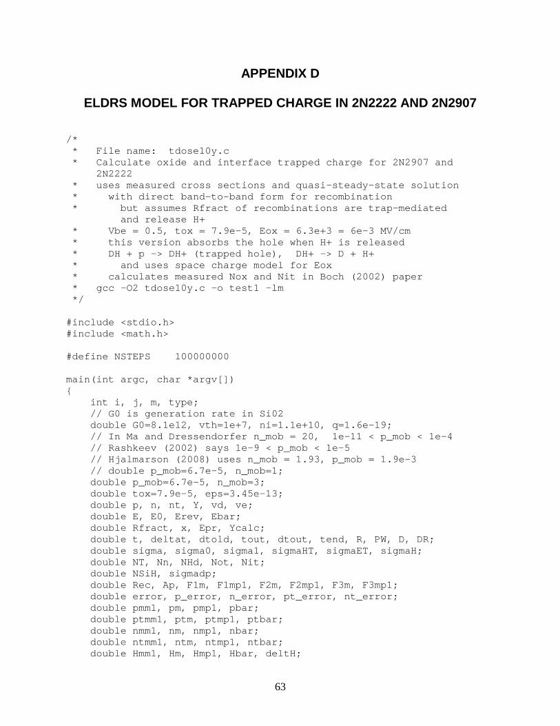
APPENDIX D
ELDRS MODEL FOR TRAPPED CHARGE IN 2N2222 AND 2N2907
/* * File name: tdose10y.c * Calculate oxide and interface trapped charge for 2N2907 and 2N2222 * uses measured cross sections and quasi-steady-state solution * with direct band-to-band form for recombination * but assumes Rfract of recombinations are trap-mediated and release H+ * Vbe = 0.5, tox = 7.9e-5, Eox = 6.3e+3 = 6e-3 MV/cm * this version absorbs the hole when H+ is released * DH + p -> DH+ (trapped hole), DH+ -> D + H+ * and uses space charge model for Eox * calculates measured Nox and Nit in Boch (2002) paper * gcc -O2 tdose10y.c -o test1 -lm */ #include <stdio.h> #include <math.h> #define NSTEPS 100000000 main(int argc, char *argv[]) { int i, j, m, type; // G0 is generation rate in Si02 double G0=8.1e12, vth=1e+7, ni=1.1e+10, q=1.6e-19; // In Ma and Dressendorfer n_mob = 20, 1e-11 < p_mob < 1e-4 // Rashkeev (2002) says 1e-9 < p_mob < 1e-5 // Hjalmarson (2008) uses n_mob = 1.93, p_mob = 1.9e-3 // double p_mob=6.7e-5, n_mob=1; double p_mob=6.7e-5, n_mob=3; double tox=7.9e-5, eps=3.45e-13; double p, n, nt, Y, vd, ve; double E, E0, Erev, Ebar; double Rfract, x, Epr, Ycalc; double t, deltat, dtold, tout, dtout, tend, R, PW, D, DR; double sigma, sigma0, sigma1, sigmaHT, sigmaET, sigmaH; double NT, Nn, NHd, Not, Nit; double NSiH, sigmadp; double Rec, Ap, F1m, F1mp1, F2m, F2mp1, F3m, F3mp1; double error, p_error, n_error, pt_error, nt_error; double pmm1, pm, pmp1, pbar; double ptmm1, ptm, ptmp1, ptbar; double nmm1, nm, nmp1, nbar; double ntmm1, ntm, ntmp1, ntbar; double Hmm1, Hm, Hmp1, Hbar, deltH;

64
double R1m, R1mp1, T1m, T1mp1, Bp, T2m, T2mp1, Bn; double Ngen, n_recomb, n_trans, p_recomb, p_trans; double pss, nss, p_sum, n_sum; double XR1m, XR1mp1, XR2m, XR2mp1; // type = 0; // for 2N2907 type = 1; // for 2N2222 // For 20 Krad // D = 2.0e+4; // PW =2.0e7; // DR = 0.001 rad/sec // PW =2.0e6; // DR = 0.01 rad/sec // PW =2.0e5; // DR = 0.1 rad/sec // PW =2.0e4; // DR = 1 rad/sec // PW =2.0e3; // DR = 10 rad/sec // PW =2.0e2; // DR = 100 rad/sec // PW =2.0e1; // DR = 1000 rad/sec // For 30 Krad D = 3.0e+4; // PW =3.0e7; // DR = 0.001 rad/sec // PW =3.0e6; // DR = 0.01 rad/sec // PW =3.0e5; // DR = 0.1 rad/sec // PW =3.0e4; // DR = 1 rad/sec // PW =3.0e3; // DR = 10 rad/sec PW =3.0e2; // DR = 100 rad/sec // PW =3.0e1; // DR = 1000 rad/sec tend = 2*PW; // tend = 10*PW; // dtout = tend/20; dtout = PW/20; if(type == 0) // 2N2907 NT = 1.3e+16; else if(type ==1) // 2N2222 NT = 9e+15; Nn = 2.0e14; if(type == 0) // 2N2907 NHd = 3.5e16; else if(type ==1) // 2N2222 NHd = 7.5e15; // Ma and Dressendorfer quote 2.7e-14 < sigma0 < 1.4e-13 sigma0 = 2.0e-13; // value quoted by Ning // 1e-14 < sigma < 1e-12 Coulomb attractive electron traps sigma1 = 3.0e-13; // cross section sigmaH quoted by Fleetwood (2008) = 1e-13 if(type == 0) // 2N2907 sigmaH = 1.1e-13; else if(type ==1) // 2N2222 sigmaH = 1.0e-13;

65
if(type == 0) // 2N2907 Rec = 1; else if(type ==1) // 2N2222 Rec = 1e+1; // in this run n~1e8, and Rec*n=1/taup where taup=1e-8 // Rec = 0; // fraction of recombinations that release an H+ if(type == 0) // 2N2907 Rfract = 0.06; else if(type ==1) // 2N2222 Rfract = 0.042; // E0 is in MV/cm, Eeb = 6.3e-3 if(type == 0) // 2N2907 E0 = 2.3e-3; else if(type ==1) // 2N2222 E0 = 2.3e-3; E0 *= 1e+6; // Y values consistent with Ma and Dressendorfer p. 108 if(type == 0) // 2N2907 Y = 0.055; else if(type ==1) // 2N2222 Y = 0.050; Epr = fabs(E0*1e-6); x = log10(Epr); Ycalc = 0.49*(1+tanh(1.2*x)); R = D/PW; DR = G0*Y*R; vd = E0*p_mob; ve = E0*n_mob; Bp = vd/tox; Bn = ve/tox; // sigmaHT = sigma0*pow(E0,-0.55); // sigmaET = sigma1*pow(E0,-1.5); sigmaHT = sigma0; sigmaET = sigma1; printf(" D = %.3e, PW = %.3e, R = %.3e, DR = %.3e, tox = %.3e\n", D,PW,R,DR,tox); printf(" NT = %.3e, sigma0 = %.3e, sigma1 = %.3e, Rec = %.3e\n", NT,sigma0,sigma1,Rec); printf(" pmob = %.3e, nmob = %.3e, vd = %.3e, ve = %.3e\n", p_mob,n_mob,vd,ve); printf(" E0 = %.3e, Y = %.2e, Ycalc = %.3e, Rfract = %.3e\n", E0,Y,Ycalc,Rfract); printf(" NHd = %.3e, sigmaH = %.3e\n", NHd,sigmaH); printf("\n"); t = 0; tout = 0;
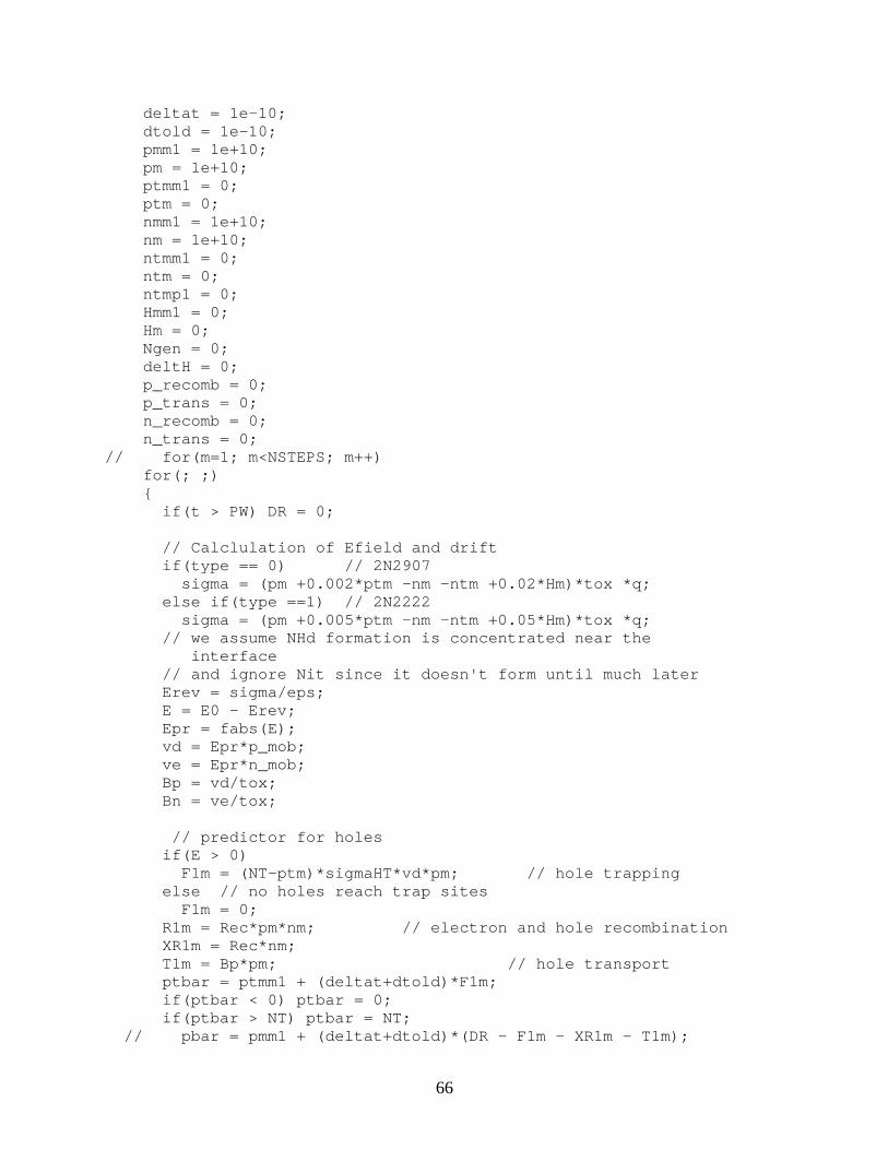
66
deltat = 1e-10; dtold = 1e-10; pmm1 = 1e+10; pm = 1e+10; ptmm1 = 0; ptm = 0; nmm1 = 1e+10; nm = 1e+10; ntmm1 = 0; ntm = 0; ntmp1 = 0; Hmm1 = 0; Hm = 0; Ngen = 0; deltH = 0; p_recomb = 0; p_trans = 0; n_recomb = 0; n_trans = 0; // for(m=1; m<NSTEPS; m++) for(; ;) { if(t > PW) DR = 0; // Calclulation of Efield and drift if(type == 0) // 2N2907 sigma = (pm +0.002*ptm -nm -ntm +0.02*Hm)*tox *q; else if(type ==1) // 2N2222 sigma = (pm +0.005*ptm -nm -ntm +0.05*Hm)*tox *q; // we assume NHd formation is concentrated near the interface // and ignore Nit since it doesn't form until much later Erev = sigma/eps; E = E0 - Erev; Epr = fabs(E); vd = Epr*p_mob; ve = Epr*n_mob; Bp = vd/tox; Bn = ve/tox; // predictor for holes if(E > 0) F1m = (NT-ptm)*sigmaHT*vd*pm; // hole trapping else // no holes reach trap sites F1m = 0; R1m = Rec*pm*nm; // electron and hole recombination XR1m = Rec*nm; T1m = Bp*pm; // hole transport ptbar = ptmm1 + (deltat+dtold)*F1m; if(ptbar < 0) ptbar = 0; if(ptbar > NT) ptbar = NT; // pbar = pmm1 + (deltat+dtold)*(DR - F1m - XR1m - T1m);
67
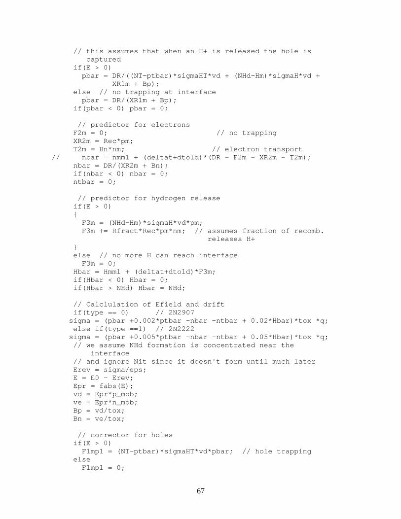
// this assumes that when an H+ is released the hole is captured if(E > 0) pbar = DR/((NT-ptbar)*sigmaHT*vd + (NHd-Hm)*sigmaH*vd + XR1m + Bp); else // no trapping at interface pbar = DR/(XR1m + Bp); if(pbar < 0) pbar = 0; // predictor for electrons F2m = 0; // no trapping XR2m = Rec*pm; T2m = Bn*nm; // electron transport // nbar = nmm1 + (deltat+dtold)*(DR - F2m - XR2m - T2m); nbar = DR/(XR2m + Bn); if(nbar < 0) nbar = 0; ntbar = 0; // predictor for hydrogen release if(E > 0) { F3m = (NHd-Hm)*sigmaH*vd*pm; F3m += Rfract*Rec*pm*nm; // assumes fraction of recomb. releases H+ } else // no more H can reach interface F3m = 0; Hbar = Hmm1 + (deltat+dtold)*F3m; if(Hbar < 0) Hbar = 0; if(Hbar > NHd) Hbar = NHd; // Calclulation of Efield and drift if(type == 0) // 2N2907 sigma = (pbar +0.002*ptbar -nbar -ntbar + 0.02*Hbar)*tox *q; else if(type ==1) // 2N2222 sigma = (pbar +0.005*ptbar -nbar -ntbar + 0.05*Hbar)*tox *q; // we assume NHd formation is concentrated near the interface // and ignore Nit since it doesn't form until much later Erev = sigma/eps; E = E0 - Erev; Epr = fabs(E); vd = Epr*p_mob; ve = Epr*n_mob; Bp = vd/tox; Bn = ve/tox; // corrector for holes if(E > 0) F1mp1 = (NT-ptbar)*sigmaHT*vd*pbar; // hole trapping else F1mp1 = 0;

68
R1mp1 = Rec*nbar*pbar; // electron and hole recombination XR1mp1 = Rec*nbar; T1mp1 = Bp*pbar; // hole transport ptmp1 = ptm + 0.5*deltat*(F1m+F1mp1); if(ptmp1 < 0) ptmp1 = 0; if(ptmp1 > NT) ptmp1 = NT; // pmp1 = pm + deltat*(DR - 0.5*(F1m+F1mp1) – 0.5*(XR1m+XR1mp1) - 0.5*(T1m+T1mp1)); // this assumes that when an H+ is released the hole is captured if(E > 0) pmp1 = DR/((NT-ptmp1)*sigmaHT*vd + (NHd-Hbar)*sigmaH*vd + XR1mp1 + Bp); else // no trapping at interface pmp1 = DR/(XR1mp1 + Bp); // steady state value if(pmp1 < 0) pmp1 = 0; // corrector for electrons F2mp1 = 0; // no trapping XR2mp1 = Rec*pmp1; T2mp1 = Bn*nbar; // electron transport // nmp1 = nm + deltat*(DR - 0.5*(F2m+F2mp1) – 0.5*(T2m+T2mp1)); nmp1 = DR/(XR2mp1 + Bn); // steady state value if(nmp1 < 0) nmp1 = 0; ntmp1 = 0; // corrector for hydrogen release if(E > 0) { F3mp1 = (NHd-Hbar)*sigmaH*vd*pmp1; F3mp1 += Rfract*Rec*pmp1*nmp1; // assumes fraction of recomb. releases H+ deltH += deltat*Rfract*Rec*pmp1*nmp1; // correction for conservation calc. } else // no more H can reach interface F3mp1 = 0; Hmp1 = Hm + deltat*0.5*(F3m+F3mp1); if(Hmp1 < 0) Hmp1 = 0; if(Hmp1 > NHd) Hmp1 = NHd; if(ptmp1 > 0) pt_error = fabs(ptbar - ptmp1)/ptmp1; else pt_error = 1; error = pt_error; t += deltat; tout += deltat; Ngen += DR*deltat; p_recomb += XR1mp1*pmp1*deltat; n_recomb += XR2mp1*nmp1*deltat; p_trans += Bp*pmp1*deltat;
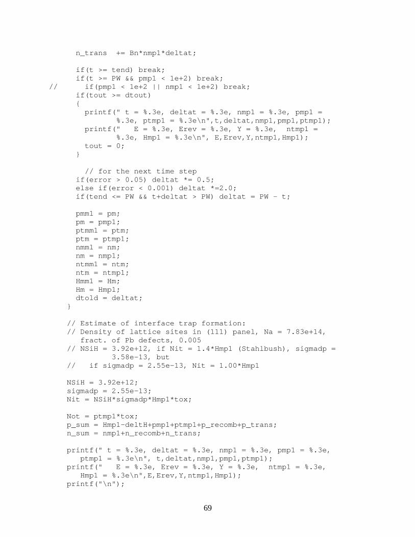
69
n_trans += Bn*nmp1*deltat; if(t >= tend) break; if(t >= PW && pmp1 < 1e+2) break; // if(pmp1 < 1e+2 || nmp1 < 1e+2) break; if(tout >= dtout) { printf(" t = %.3e, deltat = %.3e, nmp1 = %.3e, pmp1 = %.3e, ptmp1 = %.3e\n",t,deltat,nmp1,pmp1,ptmp1); printf(" E = %.3e, Erev = %.3e, Y = %.3e, ntmp1 = %.3e, Hmp1 = %.3e\n", E,Erev,Y,ntmp1,Hmp1); tout = 0; } // for the next time step if(error > 0.05) deltat *= 0.5; else if(error < 0.001) deltat *=2.0; if(tend <= PW && t+deltat > PW) deltat = PW - t; pmm1 = pm; pm = pmp1; ptmm1 = ptm; ptm = ptmp1; nmm1 = nm; nm = nmp1; ntmm1 = ntm; ntm = ntmp1; Hmm1 = Hm; Hm = Hmp1; dtold = deltat; } // Estimate of interface trap formation: // Density of lattice sites in (111) panel, Na = 7.83e+14, fract. of Pb defects, 0.005 // NSiH = 3.92e+12, if Nit = 1.4*Hmp1 (Stahlbush), sigmadp = 3.58e-13, but // if sigmadp = 2.55e-13, Nit = 1.00*Hmp1 NSiH = 3.92e+12; sigmadp = 2.55e-13; Nit = NSiH*sigmadp*Hmp1*tox; Not = ptmp1*tox; p_sum = Hmp1-deltH+pmp1+ptmp1+p_recomb+p_trans; n_sum = nmp1+n_recomb+n_trans; printf(" t = %.3e, deltat = %.3e, nmp1 = %.3e, pmp1 = %.3e, ptmp1 = %.3e\n", t,deltat,nmp1,pmp1,ptmp1); printf(" E = %.3e, Erev = %.3e, Y = %.3e, ntmp1 = %.3e, Hmp1 = %.3e\n",E,Erev,Y,ntmp1,Hmp1); printf("\n");

70
if(type == 0) printf(" Running 2N2907 from tdose10y\n"); else if(type == 1) printf(" Running 2N2222 from tdose10y\n"); printf(" D = %.3e, PW = %.3e, R = %.3e, tend = %.3e, Ngen = %.3e\n", D,PW,R,tend,Ngen); printf(" pmp1= %.3e, ptmp1= %.3e, p_recomb= %.3e, p_trans= %.3e, sum= %.3e\n", pmp1,ptmp1,p_recomb,p_trans,p_sum); printf(" nmp1= %.3e, ntmp1= %.3e, n_recomb= %.3e, n_trans= %.3e, sum= %.3e\n",nmp1,ntmp1,n_recomb,n_trans,n_sum); printf(" t = %.3e, Not = %.3e, Nit = %.3e\n", t,Not,Nit); }
71
APPENDIX E
ELDRS MODEL FOR TRAPPED CHARGE IN LPNP AND SPNP DEVICES
/* * File name: tdose13y.c * Calculate oxide and interface trapped charge for Lateral and substrate PNP BJT * uses measured cross sections and quasi-steady-state solution * with direct band-to-band form for recombination * but assumes Rfract of recombinations release H+ * Vbe = 0.7, tox = 5.7e-5, Eox = 1.23e+4 V/cm * to use this value of Eox you need to lower p_mob and n_mob * if Eox and n_mob are too high, electrons leave and can't recombine * this version absorbs the hole when H+ is released * DH + p -> DH+ (trapped hole), DH+ -> D + H+ * and uses space charge model with screening for Eox * calculates measured Nox and Nit in Witczak, etal (1996) * gcc -O2 tdose13y.c -o test1 -lm */ #include <stdio.h> #include <math.h> #define NSTEPS 100000000 main(int argc, char *argv[]) { int i, j, m, type; // G0 is generation rate in Si02 double G0=8.1e12, vth=1e+7, ni=1.1e+10, q=1.6e-19; // In Ma and Dressendorfer (3.2.2) n_mob = 20, 1e-11 < p_mob < 1e-4 // Rashkeev (2002) says 1e-9 < p_mob < 1e-5 // Hjalmarson (2008) uses n_mob = 1.93, p_mob = 1.9e-3 // double p_mob=6.7e-5, n_mob=10; double p_mob=6.7e-5, n_mob=3; // double p_mob=6.7e-5, n_mob=1; double tox = 0.57e-4, eps=3.45e-13; double p, n, nt, Y, vd, ve, Usrh, Vpr; double E, E0, Erev, Ebar; double Rfract, x, Epr, Ycalc; double t, deltat, dtold, tout, dtout, tend, R, PW, D, DR; double sigma, sigma0, sigma1, sigmaHT, sigmaET, sigmaH; double NT, Nrec, NHd, Not, Nit; double NSiH, sigmadp; double Rec, Ap, F1m, F1mp1, F2m, F2mp1, F3m, F3mp1;

72
double error, p_error, n_error, pt_error, nt_error; double pmm1, pm, pmp1, pbar; double ptmm1, ptm, ptmp1, ptbar; double nmm1, nm, nmp1, nbar; double ntmm1, ntm, ntmp1, ntbar; double Hmm1, Hm, Hmp1, Hbar, deltH; double R1m, R1mp1, T1m, T1mp1, Bp, T2m, T2mp1, Bn; double Ngen, n_recomb, n_trans, p_recomb, p_trans; double pss, nss, p_sum, n_sum; double XR1m, XR1mp1, XR2m, XR2mp1; type = 1; // for LPNP // type = 0; // for SPNP // For 20 Krad D = 2.0e+4; PW =2.0e7; // DR = 0.001 rad/sec // PW =2.0e6; // DR = 0.01 rad/sec // PW =2.0e5; // DR = 0.1 rad/sec // PW =2.0e4; // DR = 1 rad/sec // PW =2.0e3; // DR = 10 rad/sec // PW =2.0e2; // DR = 100 rad/sec // PW =6.66e1; // DR = 300 rad/sec tend = 2*PW; // tend = 10*PW; // dtout = tend/20; dtout = PW/20; deltat = 1e-10; dtold = 1e-10; if(type) { NT = 2.8e+16; // for LPNP NHd = 7.0e16; // for LPNP } else { NT = 2.8e+16; // for SPNP NHd = 1.5e16; // for SPNP } Nrec = 2.0e14; // Ma and Dressendorfer quote 2.7e-14 < sigma0 < 1.4e-13 sigma0 = 2.0e-13; // value quoted by Ning // 1e-14 < sigma < 1e-12 Coulomb attractive electron traps sigma1 = 6.0e-14; // cross section sigmaH quoted by Fleetwood (2008) = 1e-13 sigmaH = 2.6e-13; if(type) Rec = 1.5e+3; // for LPNP

73
else Rec = 1.5e+3; // for SPNP // in this run, n~1e2 and Rec*n=1/taup where taup=2e-5 // Rec = 0; // fraction of recombinations that release an H+ if(type) Rfract = 0.031; // for LPNP else Rfract = 0.013; // for SPNP // E0 is in MV/cm, Eeb = 1.23e-2 E0 = 0.006; // E0 = 0.012; E0 *= 1e6; // Y values consistent with Ma and Dressendorfer p. 108 if(type) Y = 0.06; // for LPNP else Y = 0.055; // for SPNP Epr = fabs(E0*1e-6); x = log10(Epr); Ycalc = 0.49*(1+tanh(1.2*x)); Vpr = tox*E0; // Usrh=0.5*sigma1*vth*Nrec*ni*(exp(Vpr/0.0258)- 1)/(exp(Vpr/0.0516)+1); R = D/PW; DR = G0*Y*R; vd = E0*p_mob; ve = E0*n_mob; Bp = vd/tox; Bn = ve/tox; // sigmaHT = sigma0*pow(E0,-0.55); // sigmaET = sigma1*pow(E0,-1.5); printf(" D = %.3e, PW = %.3e, R = %.3e, DR = %.3e, tox = %.3e\n", D,PW,R,DR,tox); printf(" NT = %.3e, sigma0 = %.3e, sigma1 = %.3e, Rec = %.3e\n", NT,sigma0,sigma1,Rec); printf(" pmob = %.3e, nmob = %.3e, vd = %.3e, ve = %.3e\n", p_mob,n_mob,vd,ve); printf(" E0 = %.3e, Y = %.2e, Ycalc = %.3e, Rfract = %.3e\n", E0,Y,Ycalc,Rfract); printf(" NHd = %.3e, sigmaH = %.3e\n", NHd,sigmaH); // printf(" Usrh = %.3e\n", Usrh); printf("\n"); t = 0; tout = 0; pmm1 = 1e+10;
74
pm = 1e+10; ptmm1 = 0; ptm = 0; nmm1 = 1e+10; nm = 1e+10; ntmm1 = 0; ntm = 0; ntmp1 = 0; Hmm1 = 0; Hm = 0; Ngen = 0; deltH = 0; p_recomb = 0; p_trans = 0; n_recomb = 0; n_trans = 0; // for(m=1; m<NSTEPS; m++) for(; ;) { if(t > PW) DR = 0; // Calclulation of Efield and drift // sigma = (pm +ptm -nm -ntm +Hm)*tox *q; sigma = (pm +0.005*ptm -nm -ntm +0.12*Hm)*tox *q; // we assume NHd formation is concentrated near the interface // and ignore Nit since it doesn't form until much later Erev = sigma/eps; E = E0 - Erev; Epr = fabs(E); vd = Epr*p_mob; ve = Epr*n_mob; Bp = vd/tox; Bn = ve/tox; // predictor for holes if(E > 0) F1m = (NT-ptm)*sigma0*vd*pm; // hole trapping else // no holes reach trap sites F1m = 0; R1m = Rec*pm*nm; // electron and hole recombination XR1m = Rec*nm; T1m = Bp*pm; // hole transport ptbar = ptmm1 + (deltat+dtold)*F1m; if(ptbar < 0) ptbar = 0; if(ptbar > NT) ptbar = NT; // pbar = pmm1 + (deltat+dtold)*(DR - F1m - XR1m - T1m); // this assumes that when an H+ is released the hole is captured if(E > 0) pbar = DR/((NT-ptbar)*sigma0*vd + (NHd-Hm)*sigmaH*vd + XR1m + Bp);
75
else // no trapping at interface pbar = DR/(XR1m + Bp); if(pbar < 0) pbar = 0; // predictor for electrons F2m = 0; // no trapping XR2m = Rec*pm; T2m = Bn*nm; // electron transport // nbar = nmm1 + (deltat+dtold)*(DR - F2m - XR2m - T2m); nbar = DR/(XR2m + Bn); if(nbar < 0) nbar = 0; ntbar = 0; // predictor for hydrogen release if(E > 0) { F3m = (NHd-Hm)*sigmaH*vd*pm; F3m += Rfract*Rec*pm*nm; // assumes fraction of recomb. releases H+ } else // no more H can reach interface F3m = 0; Hbar = Hmm1 + (deltat+dtold)*F3m; if(Hbar < 0) Hbar = 0; if(Hbar > NHd) Hbar = NHd; // Calclulation of Efield and drift // sigma = (pbar +ptbar -nbar -ntbar +Hbar)*tox *q; sigma = (pbar +0.005*ptbar -nbar -ntbar + 0.12*Hbar)*tox *q; // we assume NHd formation is concentrated near the interface // and ignore Nit since it doesn't form until much later Erev = sigma/eps; E = E0 - Erev; Epr = fabs(E); vd = Epr*p_mob; ve = Epr*n_mob; Bp = vd/tox; Bn = ve/tox; // corrector for holes if(E > 0) F1mp1 = (NT-ptbar)*sigma0*vd*pbar; // hole trapping else F1mp1 = 0; R1mp1 = Rec*nbar*pbar; // electron and hole recombination XR1mp1 = Rec*nbar; T1mp1 = Bp*pbar; // hole transport ptmp1 = ptm + 0.5*deltat*(F1m+F1mp1); if(ptmp1 < 0) ptmp1 = 0; if(ptmp1 > NT) ptmp1 = NT; // pmp1 = pm + deltat*(DR - 0.5*(F1m+F1mp1) –
76
0.5*(XR1m+XR1mp1) - 0.5*(T1m+T1mp1)); // this assumes that when an H+ is released the hole is captured if(E > 0) pmp1 = DR/((NT-ptmp1)*sigma0*vd + (NHd-Hbar)*sigmaH*vd + XR1mp1 + Bp); else // no trapping at interface pmp1 = DR/(XR1mp1 + Bp); // steady state value if(pmp1 < 0) pmp1 = 0; // corrector for electrons F2mp1 = 0; // no trapping R1mp1 = Rec*pbar; XR2mp1 = Rec*pbar; T2mp1 = Bn*nbar; // electron transport // nmp1 = nm + deltat*(DR - 0.5*(F2m+F2mp1) – 0.5*(T2m+T2mp1)); nmp1 = DR/(XR2mp1 + Bn); // steady state value if(nmp1 < 0) nmp1 = 0; ntmp1 = 0; // corrector for hydrogen release if(E > 0) { F3mp1 = (NHd-Hbar)*sigmaH*vd*pmp1; F3mp1 += Rfract*Rec*pmp1*nmp1; // assumes fraction of recomb. releases H+ deltH += deltat*Rfract*Rec*pmp1*nmp1; // correction for conservation calc. } else // no more H can reach interface F3mp1 = 0; Hmp1 = Hm + deltat*0.5*(F3m+F3mp1); if(Hmp1 < 0) Hmp1 = 0; if(Hmp1 > NHd) Hmp1 = NHd; if(ptmp1 > 0) pt_error = fabs(ptbar - ptmp1)/ptmp1; else pt_error = 1; error = pt_error; t += deltat; tout += deltat; Ngen += DR*deltat; p_recomb += XR1mp1*pmp1*deltat; n_recomb += XR2mp1*nmp1*deltat; p_trans += Bp*pmp1*deltat; n_trans += Bn*nmp1*deltat; Usrh = 0.25*sigma1*vth*Nrec*(pmp1+nmp1); if(t >= tend) break; if(t >= PW && pmp1 < 1e+2) break; // if(pmp1 < 1e+2 || nmp1 < 1e+2) break;
77
if(tout >= dtout) { printf(" t = %.3e, deltat = %.3e, nmp1 = %.3e, pmp1 = %.3e, ptmp1 = %.3e\n", t,deltat,nmp1,pmp1,ptmp1); printf(" E = %.3e, Erev = %.3e, Y = %.3e, ntmp1 = %.3e, Hmp1 = %.3e\n",E,Erev,Y,ntmp1,Hmp1); tout = 0; } // for the next time step if(error > 0.05) deltat *= 0.5; else if(error < 0.001) deltat *=2.0; if(tend <= PW && t+deltat > PW) deltat = PW - t; pmm1 = pm; pm = pmp1; ptmm1 = ptm; ptm = ptmp1; nmm1 = nm; nm = nmp1; ntmm1 = ntm; ntm = ntmp1; Hmm1 = Hm; Hm = Hmp1; dtold = deltat; } // Estimate of interface trap formation: // Density of lattice sites in (111) panel, Na = 7.83e+14, fract. of Pb defects, 0.005 // NSiH = 3.92e+12, if Nit = 1.4*Hmp1*tox (Stahlbush), sigmadp = 3.58e-13, but // if sigmadp = sighmaH, Nit = 1.02*Hmp1 NSiH = 3.92e+12; sigmadp = 2.6e-13; Nit = NSiH*sigmadp*Hmp1*tox; Not = ptmp1*tox; p_sum = Hmp1-deltH+pmp1+ptmp1+p_recomb+p_trans; n_sum = nmp1+n_recomb+n_trans; printf(" t = %.3e, deltat = %.3e, nmp1 = %.3e, pmp1 = %.3e, ptmp1 = %.3e\n",t,deltat,nmp1,pmp1,ptmp1); printf(" E = %.3e, Erev = %.3e, Y = %.3e, ntmp1 = %.3e, Hmp1 = %.3e\n",E,Erev,Y,ntmp1,Hmp1); printf("\n"); if(type) printf(" Running LPNP, tdose13y\n"); else printf(" Running SPNP, tdose13y\n"); printf(" D = %.3e, PW = %.3e, R = %.3e, tend = %.3e, Ngen =
78
%.3e\n", D,PW,R,tend,Ngen); printf(" pmp1= %.3e, ptmp1= %.3e, p_recomb= %.3e, p_trans= %.3e, sum= %.3e\n", pmp1,ptmp1,p_recomb,p_trans,p_sum); printf(" nmp1= %.3e, ntmp1= %.3e, n_recomb= %.3e, n_trans= %.3e, sum= %.3e\n",nmp1,ntmp1,n_recomb,n_trans,n_sum); printf(" t = %.3e, Not = %.3e, Nit = %.3e\n", t,Not,Nit); }
79
DISTRIBUTION
1 MS0352 J. Bryson, 1344
1 MS0352 C. Hembree, 1344
1 MS0525 S. D. Wix, 1734
1 MS0525 A. Nunez, 1734
1 MS0525 B. Conder, 1734
1 MS0525 R. Thompson, 1734
1 MS0525 J. Marchiondo, 1734
1 MS0807 P. M. Campbell, 9328
1 MS0807 D. N. Shirley, 9328
1 MS1072 F. Sexton, 1752
1 MS1072 P. Dodd, 1752
1 MS1072 M. Shaneyfelt, 1752
1 MS1072 N. Nowlin, 1754
1 MS1072 C. Begay, 1754
1 MS1179 L. J. Lorence, 1341
1 MS1179 H.P. Hjalmarson, 1341
1 MS1243 S. Lott, 5510
1 MS1322 J. Aidun, 1425
1 MS1323 S. Hutchinson, 1445
1 MS1323 E. Keiter, 1445
1 MS9154 W. P. Ballard, 8200
1 MS0899 Technical Library, 9536 (electronic)

80

OFFICIAL USE ONLY