development of a high bandwidth preamplifier and ...iubphys/undergraduate/theses/behnke.pdf ·...
TRANSCRIPT

A
THESIS
SUBMITTED IN PARTIAL FULFILLMENT OF THE REQUIREMENTS
FOR THE HONORS DEGREE OF
BACHELOR OF SCIENCE IN PHYSICS
Development of a High Bandwidth Preamplifier and Associated Components for the PICASSO Dark Matter
Detector
Edward Roland Behnke
August 25,2004
Supervisor: Signature Dr. Ilan Levine
Co-signer
Dr. Richard Van Kooten

A
THESIS
SUBMITTED IN PARTIAL FULFILLMENT OF THE REQUIREMENTS
FOR THE HONORS DEGREE OF
BACHELOR OF SCIENCE IN PHYSICS
Development of a High Bandwidth Preamplifier and Associated Con~ponents for the PICASSO Dark Matter
Detector
Edward Roland Behnke
Supervisor: Signature Dr. Ilan Levine
Co-signer
Dr. Richard Van Kooten

A
THESIS
SUBMITTED nu PARTIAL FULFILLMENT OF THE REQUIREMENTS
FOR THE HONORS DEGREE OF
BACHELOR OF SCIENCE IN PHYSICS
Development of a High Bandwidth Preamplifier and Associated Components for the PICASSO Dark Matter
Detector
Edward Roland Behnke
Department of Physics Indiana University
August 26,2004
Supervisor: Signature Dr. Ilan Levine
Co-signer Signature Dr. Richard Van Kooten


Contents
1 Purpose of this Document ............................................................................................... 1 2 Dark Matter ...................................................................................................................... 1 3 Picasso Overview ............................................................................................................. 4
.......................................................................................................... 3.1 IUSB's Responsibilities -5 ............................................................ 4 IUSB Preamp Conceptually and its Performance 6
.............................................................................................. 4.1 Motivation for the IUSB Design 6 ............................................................. ............................. 4.2 The Start of the IUSB Project .... 6
4.3 What has been accomplished to Date ....................................................................................... 6 4.4 General IUSB Design Goals .................................................................................................... 7
5 Preamp electrical Properties ........................................................................................... 7 6 Preamp design .................................................................................................................. 8
6.1 Op amp selection criteria ......................................................................................................... 8 ......................................................................................................... 6.2 On board power supplies -8
................................................................................................................ 6.3 Temperature sensors -8 6.4 High Pass filter design ............................................................................................................. 8
............................................................................................................. 6.5 Low pass filter design -8 ...................................................................................................................... 6.6 DC level shifting 8
6.7 Synthetic Grounding ................................................................................................................ 8 ............................................................................................ 7 Construction of the Preamp 9
..................................................................................................... 7.1 Circuit Board Layout Tools 9 7.2 Board Printing Methodology ................................................................................................... 9
...................................................................................... 7.3 Board Etching Tools and techniques 1 ................................................................................................................ 7.4 Drilling and cutting 12
7.5 Silver plating .......................................................................................................................... 12 7.6 Via techniques without plated through holes ......................................................................... 13
......................................................................................................... 7.7 Solder paste application 13 ................................................................................................................ 7.8 Parts application 1 4
............................................................................................... 7.9 Solder reflow in toaster oven 14 ................................................................................................................ 7.10 Trim and touchup 1 5
.......................................................................................... 7.1 1 Adding parts to bottom of board 15 ............................................................................................................ 7.12 Power Off Testing 1 6
.................................................................................................................... 7.13 Final assembly 1 6 .......................................................................................................................... 7.14 DC testing 1 6
7.15 AC testing ............................................................................................................................ 16 ........................................................................... 7.16 Characterization of electrical parameters 1 6
............................................................................................................... 7.1 7 Signal Acquisition 1 6 ................................................................................................ 8 Piezoelectric Transducer 17
................................................................................. 8.1 Piezoelectric Transducer Construction -17 ................... ....................................................... 8.1.1 Choice of Piezoelectric Element ... 19
................................................................................................ 8.1.2 Construction of Housing 1 9 ............................................................................................. 8.1.3 Construction of Wear Plate 19
..................................................................................................................... 8.1.4 Assembly 1 9 ............................................................................................................................. 8.1.5 Testing 19
9 Future work planned ...................................................................................................... 20 1

Contents
9.1 Quad Preamp with Temperature Sensors and Test Fixture .................................................... 20 ............... 9.2 Potential Bubble Healing Using Sound Waves or A Pre-Amp Head Test Method 20
................................................................................................................. 1 0 Attachments 2 1 ................................................................................................................................ 10.1 Funding 21
............................................................................................................................ 10.2 Schematics 22 ............................................................................................... 10.2.1 Current Implementation -22
............................................................................................................ 10.2.2 Head Assembly -24 ........................................................................................... 10.3 Attached PICASSO Documents 24
................................................................................................. 10.3.1 Summer Meeting Notes 24 . . ...................................................................................... 10.3.2 Notes fiom Patent Application 36 10.4 PowerPoint Presentations ..................................................................................................... 51
................................................................................................... 10.4.1 Argonne Powerpoint 5 1 ................................................................... 10.4.2 Montreal First Annual Bubble Conference 61 .
............................................................................................... 10.4.3 Spring APS Powerpoint -67 1 1 References .................................................................................................................... 75

Development of a High Bandwidth Preamplifier and Associated Components for the PICASSO Dark Matter
Detector
Edward R Behnke Indiana University Bloomington and Indiana University South Bend
August 26 ,2004
Abstract. The goal of this project was to expand the bandwidth of the PICASSO detector (at least for our investigative purposes), both to higher and lower frequencies, to insure that all relevant signals are being sensed. In addition, as a result of various meetings we are attempting to complete a preamp assembly, to compete for installation in the October 2004 1 Kg detector, to be placed in the Sudbury Mine in Canada. We have also developed a method to manufacture piezoelectric transducers, which promise to save considerable monies for the group, and have proposed a system of four detectors (heads) feeding into a single output channel placed in a ring around the circumference of the detector, as a way of increasing sensitivity, using our low cost transducers. To expand the measurable frequencies (most of the energy appears to be in the audio range - around 5 Hz), we are working with audio frequency transducers, both condenser microphones (related to capacitors) and dynamic microphones (speaker type devices - small electric motors). We will also be working with much higher frequency piezoelectric transducer, than the currently used commercial transducer, to expand the higher frequency areas (we don't expect much of result here, because of the predicted attenuation rate at high frequencies of the detector's constituent gel at high frequencies). Other ideas which show promise are some sort of device, like a solenoid, which would impart a square wave pulse (very broad frequency response waveform) to allow the gated sensors to be tested individually during the compression phase of the measurement cycle. We are investigating temperature sensors arrangements and electronics, which could either be built into the piezoelectric transducers or encapsulated in a similar cap. Additionally, we are investigating the development of a multipurpose transducer, each containing a piezoelectric sensor for high frequencies (high audio to 1 MHz), a condenser transducer for audio (50 Hz to 29 KHz) and a temperature sensor, and possibly including all up front or core electronics. This document covers the pre-amplifier design, operation, and manufacturing techniques, but also touches on most of the above.
1 Purpose of this Document The purpose of this document is to provide a history and some details of my nearly one and a half year involvement with the IUSB Picasso research group. The project has involved considerable effort to setup a lab, design the necessary electronics (which has resulted in a provisional patent involving an aspect of the pre-amp), create and document manufacturing techniques, fabricate assemblies, and design test fwtures, which are allowing us to investigate bubble detection physics for the PICASSO project. Also appended to the end are the Powerpoint notes fiom five talks I gave during this time and notes associated with Picasso collaboration and the provisional patent. I make no pretense to have written every word contained herein, but all mistakes are solely mine.
2 Dark Matter One of the longest standing and most important questions [l] in astrophysics and particle physics is "what is the dark matter?" Since the mid 1930s [2] there has been evidence that there is more
1

gravitating material in objects larger than the scale of a star, than can be accounted for by the amount of light coming fiom those objects[3]. The evidence has become more convincing and more detailed, including for example the observations of X-ray data fiom gravitationally bound heated gases [4] and the gravitational lensing of distant galaxies [5]. Also, evidence has accumulated that the deficit of light fiom all of this extra mass is not because the mass is concentrated in clumps of ordinary matter, such as high mass planets [6]. Even more recently, studies of the asymmetries in the distribution of relic radiation from the last scattering in the early universe [7] make a compelling case that a large fraction of gravitating matter stopped interacting with ordinary matter (protons, electron, neutrons, etc) just after the Big Bang.
The neutralino, a particle predicted by generic extensions [8] of the standard description of particles and their interactions, and assumed to have normal weak nuclear interactions with ordinary matter, is a prime candidate for the dark matter. The lightest (but still very massive) of the supersymmetric partners to ordinary matter, neutralinos, should be the sole relic of this class of particles created in the big bang. There are a number of direct search techniques [9] being developed to find evidence for the existence of these primordial Weakly Interacting Massive Particles (WIMPS). The common point of all these searches is to look for nuclei of ordinary matter which appear to get scattered for no apparent reason (The incoming WIMP would not be seen, since it does not interact with ordinary matter through the strong force, or the electromagnetic force.) The rate of these interactions should change as a function of time of year, since the earth changes its direction of motion and thus relative kinetic energy of the detector target nuclei with respect to the galactic cloud of WIMPS, as illustrated in figure 1. The annual modulation of this nuclear scattering rate is the signal being searched for by all operating dark matter search experiments. (In addition to an annual modulation, some future experiments will try to measure the direction of the WIMPS by looking at the direction of the nuclear recoils.) With a problem as central as the search for dark matter, complementary approaches are important.
Of the several pieces of evidence, I will discuss two. The fust is the orbital velocities of stars on the outskirts of galaxies. One such galaxy is shown below; you will note an easily identifiable central mass and a thin sheet of stars forming the outskirts of the galaxy. Newton's laws predict the velocity of a star outside the clearly defined central mass as:
From this we would expect that the velocity of a star farther fiom the central mass would be less than a star closer to the central mass. This is not what is seen.
If instead of assuming a central mass we assume a uniform mass distribution, Newton's formula becomes:
2

Again, this is not what is seen. What is seen is that velocities in the outskirts remain relatively constant. One can guess that this is because both of the above models are in operation; essentially causing a fixed velocity of the stars in the outskirts and that some unseen mass is being observed resulting in the apparent velocity discrepancies. This is approximately what is seen.
Galaxy with Central Mass
A second piece of evidence is that of excess gravitational lensing. General Relativity predicts gravitational lensing or bending of light due to the perturbing presence of matter. In the figure below you can see the effect of a large cluster of galaxies on a distant galaxy as viewed from an observer's perspective. This is the expected result. If the mass distribution were uniform enough and the observed galaxy centered directly behind the cluster, a halo would be observed around the cluster of galaxies. The problem is that the amount of bending that is measured in our picture is ten times what the observed visible mass would cause.

- - - - - - - - - - -
Gravitational Lensing of Light from a Distant Galaxy
One example of gravitation lensing - note the smears or partial halos of light
3 Picasso Overview The PICASSO ( htt1~ j~ic'1\\0 1p5 L I I I I O I ~ I ~ cLt1 LC! ) collaboration's [lo] approach exploits the bubble chamber technique developed by Glaser [I I], as adapted for neutron dosimetry by Apfel [12] to try to listen to the results of WIMP collisions with Fluorine nuclei in moderately superheated droplet detectors [DD]. DD serve as both the neutralino target and the nuclear recoil detectors. The detectors consist of a polymerized gel which suspends liquid droplets in a superheated state. The
Freon-like liquids (e.g. C4FI0 and C3F8) are kept at temperatures above their normal boiling point (Tb= -1.7 OC, Tb= -36.7 OC, respectively.) According to the standard theory of bubble chambers (eg. as in the classic paper by Seitz [13]), these superheated liquids undergo explosive phase transformation to a gas, if a sufficient energy "spike" is deposited in a small enough volume, for example by a nucleus recoiling from scattering by a WIMP (The detectors have sensitivity to neutron kinetic energies as low as 10keV.) The majority of the energy of this phase transition is emitted in acoustic waves. The PICASSO collaboration has been attempting to detect [14] WIMP interactions, by detecting these acoustic signals.
This technique has several attractive features. First, in the case that the neutralino interaction is spin dependent, rather than coherent, the WIMP cross section with 1 9 ~ is higher than for any other nucleus, meaning that a smaller amount of target material is required for a given sensitivity. Second, the technique is relatively insensitive to most background radiation. In principle, radioactive contamination of detector materials is one of the biggest problems that this type of experiment needs to overcome, since the decay products (a,P,y, recoiling decay nuclei) can mimic the signal. The DD technique has the advantage that, with the proper operating conditions, the detector is insensitive to P,y and minimum ionizing particles. Third, the detector should be relatively inexpensive to manufacture and purifjr (-$50,00O/ton active material.) Fourth, the detector can be operated at roughly room temperature. Fifth, it is possible to add complementary event detection ability with the addition of liquid scintillator to the droplet mixture.
3.1 IUSB's Responsibilities Many technical problems need to be overcome on the way to a 103kg detector (shown schematically in figure 4). The IUSB team has taken responsibility for studying acoustic properties of the detector (Attenuation length, speed of sound, frequency content as a function of droplet size, event selection criteria, and event localization.) These become more important to understand in detail as the size of the detector grows. It is crucial to know how large detectors can be made without losing efficiency for signals far from the sensors. Studying the event frequency and amplitude as a function of droplet size will help one understand the efficiency of the detector and will help in developing event selection criteria to reject acoustic or electrical signals from sources other than true bubble events. Event localization will be important in attempting to eliminate "hot" regions in the detector.
IUSB will also be studying different types of acoustic sensors and placement of the sensors. Ideally, the sensors would be placed on the inside walls of the detectors so that they would couple acoustically to the gel directly, rather than having the signals travel through the container walls as they do now. But this requires finding sensors that will not be damaged by being submerged in the caustic gel, and which will not be sources of radioactive contamination, which would trigger bubbles.
4 IUSB Preamp Conceptually and its Performance
4.1 Motivation for the IUSB Design The current PICASSO preamplifier is bandwidth limited at somewhere below 1 MHz. Phase shifting and decreasing gain set in at about this point. Thus all measured responses occur below this point. We at IUSB decided that the preamp should not be a limiting factor in the bandwidth, within the constraints of current technology. We set out to design a circuit with a bandwidth of at least 5 MHz. We can go much higher, but the current piezoelectric transducers which we have found seem to set this as an upper limit. This may in fact be more bandwidth than the current experiment needs, but will allow room to grow.
The problems encountered in this design and the solutions to them are the topic of this paper.
4.2 The Start of the IUSB Project IUSB started actively participating in the PICASSO experiment starting in May, 2003. The first project was to build a low cost laboratory consisting of two PCs for data acquisition, electronic components, piezoelectric acoustic sensors, and (BTI) DDs purchased with startup funds fiom the PI, Ilan Levine, and an oscilloscope emulation card on loan fiom the UniversitC de MontrCal. A complete developmental 1-channel data acquisition system to take acoustic signals from a piezoelectric sensor, send them to a preamplifier, and from there send them to the ADC card interfaced with the data acquisition computer has been developed. Both waveforms and Fourier transforms of these signals have been studied in a preliminary fashion. In addition, the differences between these signals and generated noise signals (both acoustic and electrical), are being examined.
4.3 What has been accomplished to Date The main accomplishment has been to develop a preamplifier for reading the piezoelectric sensors with little signal loss, a flat gain over a wide frequency range, and with no DC voltage difference established across the sensor. Typical circuits found to read these devices seem to rely on the Q value for specific sensors, discard a fair portion of the signal (and thus requiring more gain-which means more noise and roll om and establish a voltage difference across the crystal, due to bias current of the op-amp ( which stresses the crystal.) The group developed what is believed to be a novel circuit which solves all of these problems, and delivers a low noise signal (with little amplification needed) and a nearly flat gain from 1,500 Hz to 2MHz. Although the response of the particular sensor currently being used is much more restricted than this range, the preamplifier was developed with the intention of testing a wide variety of sensors. The circuit has been submitted to the Indiana University office of technology transfer for possible patenting. In figure 5 the performance of the fiont end of the circuit is shown. The gain is flat from 50Hz to 5MHz. Figure 6 shows the performance of the entire circuit from 50Hz to 5MHz. The gain is roughly constant from 1,500 Hz to 2MHz. The flat response can easily be extended in both the high frequency and low frequency bands, if desired.

4.4 General IUSB Design Goals Our design goal was to build a circuit having a large bandwidth with a flat frequency response, and additionally having minimal phase shifting as a function of frequency. FET front ends seem to carry the burden of reduced high fiequency response and have reasonably large phase shifting at higher frequencies. Wanting to study higher frequency transducers we invented a method of coupling high frequency low noise op amps (which do not have FET front ends) to a piezoelectric transducer. The IUSB design reduces or removes the dc load on the transducer which could change the apparent response of the piezo, as these transducers respond to dc levels by generating a responding voltage, both to mechanical and electrical stress. We think that it is likely that this dc level could color the piezo signal we are trying to detect. The design of the IUSB circuit was motivated by the result that when our high frequency op amp was loaded by a piezo transducer has no apparent dc load allowing the output to float. To eliminate the floating we added a resistor to the input, this caused an offset voltage. This offset places physical strain on the transducer resulting in a generated voltage with leakage - the net effect was an oscillation that ensued in a couple of minutes, usually destroying all devices in the circuit. This oscillation is eliminated with the synthetic ground, the heart of the IUSB circuit.
We experimented with many types of preamps. JFET front ends were best for interfacing to the piezoelectric transducers. A piezoelectric transducer looks like a capacitor electrically but if you apply a voltage to it deforms the crystal. When trying to use a piezoelectric transducer to drive a standard op amp the inputs float away from ground. Eventually the circuit starts to oscillate and for most of our test circuits, destruction was imminent.
We solved this problem by placing a fixed load resistor across to ground to act as a high impedance reference and we then sense the resulting offset voltage with a JFET op-amp, set up as a low pass filter. The JFET op-amp then integrates the resulting signal to the average DC voltage set by the load resistor. This is then used to drive a voltage follower op amp which provides a virtual ground at the average offset voltage to the piezoelectric sensor. The net effect is to make the DC voltage across the piezo zero and stop all oscillation, allowing for high speed ultra low noise op amps to be used as the interface device.
5 Preamp electrical Properties
We, Indiana University, through the Patent Office ART1 have a provisional patent on the circuit described above - the attached notes are the formative paperwork of the application for patent. They describe the electrical properties in great detail.
As a brief summary, we achieved our goals. We have developed a very flat gain high bandwidth amplifier capable of coupling to a piezoelectric transducer. This will allow exploration of frequency spectrums - given the appropriate piezoelectric transducer - not currently explored.

6 Preamp design The input or synthetic ground section is nonstandard but the remaining stages are textbook implementations. The high pass filter is somewhat special - it is a suggestion of the manufacture Analog Devices.
6. I Op amp selection criteria We searched for the highest bandwidth op amps that we could find. They had to have a high slew rate and very low noise. This is not as straight forward as it sounds. The devices from National Semiconductor, which don't report low noise levels compare favorably with Analog Device parts which claim very low noise specifications.
6.2 On board power supplies The Picasso project uses VME crates to power the pre-amps. The onboard power supplies are a possible source of noise and coupling of individual circuits. Additionally the bench supplies we were using in the lab developed considerable noise, in the form of oscillation on the power inputs as we increased their supply voltage. The onset of oscillation occurred suddenly at a particular voltage. This seemed power supply dependant. When we inserted standard card power supplies IC's it seemed to correct the problem. The units chosen are sufficient to power a quad head.
6.3 Temperature sensors The Picasso experiment is temperature dependant. As a side thought we inserted a temperature sensor on the circuit board and intend to add a sensor to sense the temperature of the experimental gel at the location of the piezoelectric transducer. The device chosen can be calibrated, but the "off the shelf accuracy" is accurate through ow range to within about 2 degrees.
6.4 High Pass filfer design This is a specialized design to take advantage of the high band width of the op amps and is from the manufacture.
6.5 Low pass filter design This is the standard classical filter.
6.6 DC level shifting This is a set of standard tantalum electrolytic capacitors wired plus to plus to allow them to decouple and pass ac voltages. It seems to work to very high frequencies (at least 5 MHz square waves - our maximum).
6.7 Synthetic Grounding This is the novel part of our circuit. It is a method of allowing for the quiescent bias current induced offset, normal to high speed op-amps, averaging the resulting voltage, filtering it and then sending the resulting voltage level to the other side of a piezoelectric transducer as a DC level. Note the schematic and of course the patent application notes for further information.
8
7 Construction of the Preamp We will discuss some of the specialized techniques required to build the double sided surface mount assemblies we required in the final implementation.
7. f Circuit Board Layout Tools At the beginning of the project we started using DIP type devices and proto boards. We progressed to hand wired Vector boards. At this stage the schematics were developed, f ~ s t in AutoCAD LT then finally in AutoCAD. This necessitated building custom libraries of parts.
The next generation of parts was only available as surface mount parts. This meant a new piece of software needed to be found and learned. We used Eagle software Version 4.1 1r2 for Windows (www.cadsoft.de). This software, is the fiee version, it is capable of generating the art work for a double sided or two layer boards the size of a half a euro card (about 2 in x 4 in). Again the extensive library only contained some of the needed parts, so the library needed to be extended.
We encountered several problems with our first implementations. Vias which connect top traces to bottom traces are normally accomplished by plated thru holes. We did not have that capability. Our work around was to feed wire thru each hole. The software's autorouter liked to place the vias under components. This caused many problems as there was insufficient room for the wire under surface mount parts. We solved this and many more problems by limiting the location of holes and which side of the board connections were made. You will note attached schematics, traces, and component locations in the attachment section. You can get a feeling of the magnitude of the problems fiom examining these. All components are placed on the final board by hand, the traces are automatically routed by the software, based on the rules we established.
7.2 Board Printing Methodology There are several methods to make traces on copper boards. The majority of my experience was with photosensitive boards which are exposed and developed much like black and white photographs, then etched. This method is dependent of having very good light sources and a good darkroom. We had neither.
A second method that is popular is based on the fact that laser printers and copy machines transfer black plastic to paper, as their method of operation. We bought a commercially available transfer paper and spent several weeks trying to transfer an image to copper with very little luck. Because of this we purchased a modified laminator. We worked with this machine for a couple of months, never getting a very good transfer. We tried all variations of controlling cleanliness and multiple passes through the machine. Finally a call to the paper and laminator supplier yielded a method of increasing the heat output. By varying the feedback resistor on the heat selection switch, we increased the heat fiom about 200 deg F to about 500 deg F. This worked, we were actually able to transfer images to very dirty copper. This yielded boards that no longer required considerable

touch up before etching. We apply an additional green film layer to further protect the black. This is laminated on the black after removal of the paper in a water bath.
Basically the method is to print multiple copies of both sides of the traces on special transfer paper being carell to only touch the paper using rubber gloves cleaned with alcohol. This is then laminated onto a board which has been cleaned very carefully, first with unscented Dawn dishwashing soap and 400 wet dry sandpaper, then the water is removed by washing with pure alcohol. Next the paper containing the resist is drilled (alignment holes only), using the Dremel. One side is applied to the double sided very clean and slightly rough board, using Avery labels cut into thin strips. Next the alignment holes are drilled through the board and the second side is carefully aligned and taped using a light table. Both sides are laminated by using four passes - one each direction - in hopes of defeating label lifting (the label lifts the heated rollers as they pass, causing incomplete transfer. Next the cooled assembly is quickly placed into a tank of water and the paper is allowed to slowly lift off the board, leaving the plastic on the board. This is then carefully dried and a layer of green transfer film it applied to both sides and ran thru the laminator a couple of times, being very carell to keep the film stretched flat. The film is then ripped off leaving the tracks further protected by a green coating and is ready to etch, after careful inspection and touch up, using the dissecting scope, we etch the board in the etchant bath.
Etch Resist Transfer Assembly (Laminator)
This is a commercial laminator. It is usually used to laminate layers of plastic for ID badges etc. The temperature used is far too low to transfer the plastic fiom the laser printer to the circuit board
The unit we purchased was supposed to have been modified. I highly suspect it had not been. These units are available fiom office supply stores, and this brand can be modified.

7.3 Board Etching Tools and techniques We are using sodium persulfate to etch our boards. We have some ferric chloride, but haven't used it. The method requires that the fluid be warmed to about 100 deg F and that it be stirred gently throughout the etch cycle of about 30 minutes.
All the components of the purchased assembly worked fme except the stirring method.
Etching Tank Assembly
This is a commercially available tank from Digi-Key - GC.
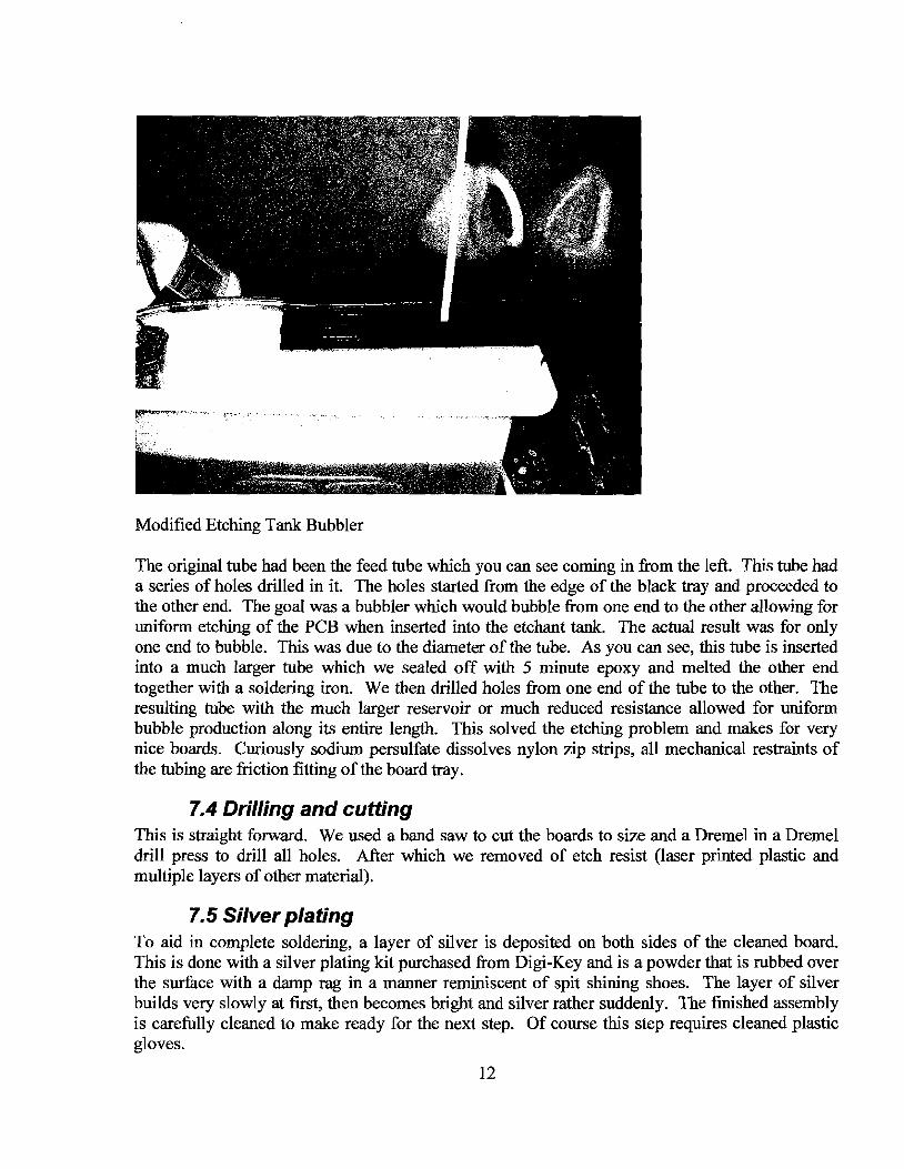
Modified Etching Tank Bubbler
The original tube had been the feed tube which you can see coming in fiom the left. This tube had a series of holes drilled in it. The holes started from the edge of the black tray and proceeded to the other end. The goal was a bubbler which would bubble fiom one end to the other allowing for uniform etching of the PCB when inserted into the etchant tank. The actual result was for only one end to bubble. This was due to the diameter of the tube. As you can see, this tube is inserted into a much larger tube which we sealed off with 5 minute epoxy and melted the other end together with a soldering iron. We then drilled holes from one end of the tube to the other. The resulting tube with the much larger reservoir or much reduced resistance allowed for uniform bubble production along its entire length. This solved the etching problem and makes for very nice boards. Curiously sodium persulfate dissolves nylon zip strips, all mechanical restraints of the tubing are friction fitting of the board tray.
7.4 Drilling and cutting This is straight forward. We used a band saw to cut the boards to size and a Dremel in a Dremel drill press to drill all holes. After which we removed of etch resist (laser printed plastic and multiple layers of other material).
7.5 Silver plating To aid in complete soldering, a layer of silver is deposited on both sides of the cleaned board. This is done with a silver plating kit purchased from Digi-Key and is a powder that is rubbed over the surface with a damp rag in a manner reminiscent of spit shining shoes. The layer of silver builds very slowly at first, then becomes bright and silver rather suddenly. The finished assembly is carefully cleaned to make ready for the next step. Of course this step requires cleaned plastic gloves.

7.6 Via techniques without plated through holes We tried many ways to form electrical connection fiom the top to the bottom of the board. The first was a purchased kit that put a hollow sleeve in each hole, which was to be crimped. This was a problem, primarily due to the size of the holes needed (too large) and was quite expensive. The next was a series of wires with a very sharp kink making a wire that would not fall through the holes. These were very time-consuming to manufacture and fell out part of the time when the board was inverted. We tried simple loops joining any two vias. This was also very time- consuming. The obvious next step was a long length of wire joining many vias, stiching - this worked quite nicely and is the technique used. This is done carefully to insure that wire touches trace on both the top and the bottom of the board. Additional care is taken to insure that the bottom loops are uniform enough for the board to set level on the cooking tray. The top is routed in such a way as to allow easy placement of components on the top of the.
Note Wire Stitching of via's
7.7 Solder paste application Solder paste is a mixture of small spheres of solder interspersed in a liquid flux. When the flux flashes off, the solder forms reliable joints on all exposed surfaces.
Again clean plastic gloves are used to prevent contamination of the surfaces. We use a hypodermic style injector with plastic tips to coat all via surfaces and wires both top and bottom

and all component pads. It is much easer to add components to finished boards if the pads have a layer of solder. All marginal traces are repaired using an application of solder paste. All excess solder paste between traces is removed by mechanical separating it or scrapping it to the nearest trace or pad. Bridged components are only a small problem, as the surface tension and component design is such to form a reliable connection if a reasonable amount of paste is applied.
Both the solder paste and the partially completed assemblies are refrigerated when not being used over night.
7.8 Parts application All top surface parts are applied to the solder paste. When we lay out a board, all polarized capacitors, diodes and chips face the same direction, allowing for easy assembly and testing. A good pair of bent tweezers is needed for parts placement. They are specially constructed to open to the correct dimensions required by normal parts, will handle the very small parts and seem to shed solder paste, or at least are very easy to clean. Surprisingly, placement of parts is quite easy, even after coffee, using the stereoscopic microscope. Some could place most parts using the naked eye.
7.9 Solder reflow in toaster oven We are using a technique found on the internet at:
It is a very usable article on how to use a common toaster oven as a solder reflow oven.
A summary of the technique is to set the temperature for 4 minutes at 200 deg F, 1.5 min at 325 deg F, and 30 sec at 425 deg F (The final measured temperatures are 150 deg, 200 deg, and 250 deg F). At the end of the cooking cycle (you can see the flux flash off and the soldering take place) the oven is tapped to seat components and the door is opened to allow cooling with the board left in the oven for a few minutes to prevent temperature shock. The board is then cleaned according to the type of flux used.

Solder Reflow Oven with Element Shield in Place
You will note that the door connection is removed or bent out of the way so that the tray will stay in the oven for cooling. This is in part to allow for a gentler cooling cycle and in part because the parts would just love to slide off the board.
7.10 Trim and touchup After cleaning, all via wires are trimmed, and the board is touched up. We use a Weller soldering station made up of a WSL temperature controller and a WMP 60 watt iron. This assembly is very well matched to the job.
7. I 1 Adding parts to bottom of board The first try at adding parts to the bottom of the boards were to apply solder paste and manually heat the part. As you might imagine the surface tension caused the very small parts to disappear into the solder on the tip of the iron. The next try was to hold the part on one end and heat to other to reflow solder left fiom the solder paste by the method described above. This worked quite well. The other end was quite easy to solder, after the first had cooled. There is a bit of magic involved in applying small components, but the finished board work quite well - meaning we didn't destroy parts during the heating cycles.
7.12 Power Off Testing At this point all components are inspected for proper orientation, all traces are inspected for shorts and or breaks, all supplies are tested for shorts using a multimeter. In general any easy problems are fixed before power is applied.
7.13 Final assembly Next the I/O connectors and wires are soldered to the board, an aluminum box is milled and connectors are added to it, stand offs are installed for the board and the unit is assembled.
7.14 DC testing Here the final assembly is again tested using a multimeter for any obvious dc problems.
7.15 A C testing This is where the power is applied. The first step is to check components for excessive heat (parts in wrong). The next step is to verify supply voltages and grounds at all IC's. The next step is to check all op amp inputs for correct voltages (amplifiers always have the same voltage on both the plus and minus inputs - comparators can have different voltages). In general, tracing from the front to the back of the circuit will show that either the board is entirely dead or functioning properly, both are quite related, so care must be taken.
7.16 Characterization of electrical parameters This is the point where all seems well and signals are applied to the inputs and followed through the entire circuit. After the circuit is shown to be working properly it can be characterized using signal generators or other types of inputs.
7.17 Signal Acquisition The next step is to use the completed assembly to acquire real signals.

8 Piezoelectric Transducer Due to the high cost of commercial transducer of about $1 50, we developed a low cost alternative. It is possible that they may prove acceptable to the experiment both as a cost savings and as a controllable fiequency range device. The following outlines their construction. Much work remains to be done. Many different elements are commercially available. The actual attachment may benefit by a circuit board to reduce heat inflow during the cap to wear plate attachment. A circuit board would also allow a multipurpose head containing a low frequency element like a condenser microphone element and an on board temperature sensor. The power supply on the pre amplifier board would easily allow for multiple sensors and off card preamplifiers to feed the main amplifier unit, summing the resulting signals into one output.
8.1 Piezoelectric Transducer Construction
Cap Assembly with BNC Connector and Wire Lead
This is a picture of the piezoelectric transducer container. It is required to provide electrical shielding, electrical connection to one side of the piezo chip and a mechanical furture to hold all the needed parts. We suspect there are many potential solutions, but this one cost 40 cents for the cap. We use a BNC connector, but other output types could be used, or even a cable bundle could exit a simple hole with a protective grommet. The faraday cage would be defeated unless shielded bundles were used and a bit of care taken at the exit.

Piezoelectric Chip with Wire Solder Pasted to Assembly
This is scrap from circuit board fabrication. One side has the copper etched off. This allows us a complete copper layer to shield the sensor in a faraday cage. These parts were joined using solder paste and our solder reflow system. Normally the wire will be joined in a separate operation, but solder paste would be applied before reflow. Great care must be taken to hold the board level as the sensor slides when the solder melts. This would probably be cured if the attachment were made into a circuit board with attachment pads. Surface tension of the solder and the edges of the pads being larger than the connecting traces should suffice to lock the transducer in place till the solder cooled.
Destructive Testing of Assembly before Trimming
This picture is of a piezoelectric assembly that failed during construction. The wire came off the top of the piezoelectric element during joining, due to the heat, rendering the assembly useless.
18

This was caused by the mechanical connection of the wire being stressed, causing the wire to separate fiom the top of the piezo chip. This was solved by bending the wire before attachment of the cap to the wear plate, to "spring" the wire in place, allowing it to stay in place even if the solder on the top melts - this method works quite nicely. This failure allowed destructive analysis. As you can see the board is quite bent and the copper torn off from the force required to pull it apart. The cap and the circuit board were joined together using solder paste fiom our surface mount supplies and a Radio Shack miniature soldering 1 torch butane tool.
8.1 .I Choice of Piezoelectric Element We are investigating a wide variety of sensors to determine which would best solve our problems. At present it seems that sensors in the audio range are best. But our preamp has opened a window that has previously been closed to the project and higher frequencies need to be investigated.
8.1.2 Construction of Housing We have adopted an easily obtainable housing, a standard end cap for copper plumbing. The criteria are only that it holds the output connector and forms a faraday cage when joined to the wear plate.
8.1.3 Construction of Wear Plate We have determined that the wear plate or the working surface of the sensor can be printed circuit board material by using a commercial sensor and looking thru a layer of the material, it seems that there is little or no attenuation. This could be an active area of investigation. Most commercial wear plates seem to be ceramic.
8.1.4 Assembly This device is made in steps.
First the cap assembly is milled and assembled, Second the piezo element is reflowed on to the wear plate, Third the cap assembly is joined to the wear plate using solder paste and a mini-torch.
8.1.5 Testing These devices either work or not. This means that you can test them either by driving them with a known good signal from a good transducer, driven by a signal generator, or look at a known good signal from a detector. We have yet to set up a standard test fixture to quickly characterize and certify working units, work which will need to occur if we build hundreds of transducers.

9 Future work planned
9.1 Quad Preamp with Temperature Sensors and Test Fixture We are planning to test a quad sensor which would consist of one output channel with 4 JFET sensors or our high fi-equency fi-ont ends implemented as head assemblies. Most of the IC7s we have worked with have the capability to be gated on and off with a integral pin. This, coupled with the pulse from a solenoid, described in the next section, would allow us to determine the health of individual piezoelectric sensors in addition to the associated electronics. This would be done during the compression phase and change in temperature period which lasts for several hours.
9.2 Potential Bubble Healing Using Sound Waves or A PreAmp Head Test Method
We plan on testing a device like a solenoid pounding on a metal plate glued to the gel vessel to both test the health of individual sensors and their electronics and to see if the gel would heal faster as the result of a bit of energy. Conceptually, if the bubble is a thousand fold expansion in size, then this creates a very large surface area, possibly during the compression phase, a bit of gas is caught in the folds of the collapsed bubble, causing re-inflation if the pressure is removed too quickly. Vibration of the gel might cause the trapped gas to be expelled faster, through a mechanism liked dynamic verses static coefficients of fiction. In any case we could test the electronics and sensors using the noise.

10 Attachments
10.1 Funding
Summer 2003 -partial travel funding was covered by an IUSB SMART Committee grant.
The Argonne Trip travel portion was covered by a IUSB SMART Committee grant.
The Montreal Trip for the First Annual Bubble Conference is to be covered in part by an IUSB SMART Committee grant.
The Spring APS meeting is to be covered by IUSB Physics Department Monies.
Material to populate lab and build circuitry came fiom IUSB and Dr. Levine's startup funds.
Specialized build equipment like Dremels, grounded tip soldering irons etc. were fiom my shop - most have or are being replaced with new equipment.
Two binocular microscopes are on generous loan fiom the IUSB Biological Sciences Department.
Josh and my time were donated in the interest of physics.

10.2 Schematics
10.2.1 Current Implementation
10.2.1.1 Schematic - Piezo Buffer - Bandpass

10.2.1.2 Top Layer
10.2.1.3 Component Placement
10.2.1.4 Bottom Layer

10.2.2 Head Assembly
10.2.2.1 Schematic - Head +
Indiana University South Bend E R B ~ ~ L . lLpvine
TITLE: Piezo Head PICASSO
Document Number: I U S B - ~ O ~ ~ - L B O O ~ ~ RT
Date: 4/29/2004 09:11:03p ISheet: 1/1
10.2.2.2 Component placement
10.3 Attached PICASSO Documents
10.3.1 Summer Meeting Notes

about 12 1, while the center has a gain of 133 1 (-63 dB). We have found a gain of about 100 useful when measuring the signals directly from the 8ml tube The data taken on the tube with a gain of 1300 had many "clipped" (events which were of too large an amplitude for our CSLITE ADC card - lvrms) and there might have been high frequency aliasing in the FFT as a result.
We have not mounted the power protection ferrite directly on the board. It is possible on future generations. We have no problem in our environment with RF piggy backing on the power. A suggestion is Digi-Key Steward EM1 Cylindrical Bead Cores part number 240-2136-ND for .59 us.
The transducers are just in their first stage of development. (A cartoon of this device is shown in appendix 11.) Nevertheless, even in this crude form, they seem to have sensitivity comparable to the commercial transducers (although as will be seen below, they don't display high frequency peaks.) Now, the parts for one of these devices cost a total of about $5, as compared with the purchase price of the commercial transducers which is about $150. They are also quite easy to construct and we can, when the time comes, produce hundreds of these at IUSB. The results are promising enough that we may be able to sufficiently develop these devices so that they can be installed as secondary sensors on the lkg detector as suggested below. We have far enough to go in the R&D of these devices that they will most likely not be good choices as a primary sensor on the short time frame before the October installation. The construction is done using a solder reflow technique for both the attachment to the Piezo and to the mounting board. As a result they are quite robust mechanically. If you wish we can construct a sample for you to do destructive testing. We have some construction ideas that we have not yet tried, but they are primarily related to construction and not life expectance. We would like to try different piezos to attempt to get more high frequencies.
10.3.1.2 Data taken with the devices: On June 10, 12, and 14, we made various measurements using the new surface mount circuit (NC), an old Vector board circuit (OC), the new (hand built) transducer (NT) and a commercial transducer (CT) identical to the ones now being used by PICASSO at SNO.
In the first set of measurements (runs 453-460), the CT and NT were coupled to an 8ml " l ~ m - spiked BTI bubble detector using duct-tape for pressure and Vaseline as acoustical coupling. A photograph of this setup is shown in figure 1 below. Initially, the CT was coupled to the NC, and the NT was coupled to the OC. The tube was activated and data was taken in a "setup" run. This run (453) was deliberately noisy. We activated and deactivated the tube, tapped the tube, and turned on a computer known to cause electrical noise in the system. Appendix III contains a set of 8 event types seen in this run ("good events", various types of noise, and one type of event which we have not yet classified as "good" or "noise.")
In subsequent runs we took data with varying circuitlpiezo combinations as well as some runs where only one sensor was used. Summaries of the seven good runs are given below. A detailed analysis of this data is needed and will be done later. General observations: The efficiencies of the two transducers seem comparable. All runs were roughly 242 seconds long and had between 36 and 43 events. The trigger was sometimes set to be from the NT and sometimes set to be from the

Figure2: Test setup for fish tank measurements. Commercial transducer coupled to end of fish tank glass using duct tape and Vaseline again. Signal being sent to new circuit (loose wires are temperature probe lines not yet connected to banana plugs. 8ml activated tube is supported by Plexiglas tank cover with insertion holes every 5cm. The tank is filled with water. The distance from the center of the tube to the ceramic face of the transducer is 2.5 cm in this instance. Seen in the upper left corner of the photograph is a home built WSB transducer.

Fish tank data: The fish tank measurements might have inadvertently been made with a gain of 100. 2.5cm, 28 events, 244sec 7.5cm, 17 events, 244sec 12.5cm, 8 events, 240sec
Rate vs dist dt15 and new amp
1 0.16, 1 I
0 ! 0 2 4 6 8 10 12 14
Tube-sensor distance (cm)
Now, the tube is spiked so that true event rate is about one event every 10 seconds or 0.1 evls. So, the result at 2.5 cm is consistent with 100% efficiency, albeit with a low statistical significance.
10.3.1.3 Other Measurements:
Flatness of gain: A rough check of the flatness of the gain was made by taking a sinusoidal signal from a signal generator, reducing the signal to a very small value and observing the preamp output voltage as the frequency of the generator was dialed from 500Hz to 5MHz. The output voltage as observed on an oscilloscope did not change appreciably with frequency.
Measurement of temperature: We read the signal coming from the surface mounted temperature probe (on the NC) using a DVM. We read voltages of X up to Y indicating temperatures of A to B.
10.3.1.4 Possibilities for development:
We have the following questionslsuggestions about the next version of the preamp: EM1 (electro magnetic interference) isolation ferrite bead location - either on the PWB or on the power cable: Parts reduction by optimizing the circuit for cost rather than performance.

Reduce the number of gain stages as we have plenty of bandwidth and could spend some on fewer devices and optimize the synthetic gnd, possibly by sharing op amps with the temp sensor. Removing some protection circuitry around the on card power supplies. Add more interface connectors to the PWB. Add more inputs per card. Given the cost of our IUSB transducer, we could use arrays of transducers, possibly 4 transducers per output card, where the signal fiom four transducers are summed into one output. We are considering building a 6 inch round tank with schedule 40 pipe and placing 2 rings each containing 4 transducers summed into one channel. If the rings are spaced 3 inches apart with the top ring centered on our bubble tube, we could test for blind spots and signal level by moving the bubble tube around in the water constrained by the top ring. This tank could be filled with jell for more realism. Each piezo input circuit can be gated (a feature of the AD8021 op amp. This would mean that if a test audio signal was supplied, the health of the detector could be tested. The signal could be one that resonates with the Freon liquid, possibly with the added advantage that we might convert the Freon to jell fiiction from static to dynamic coefficients of fiiction and reduce the healing time of micro fractures in the jell by detaching Freon fiom the side walls and hence fiom within the micro fractures in less time than the current method. Our chemistry department has a ultrasonic stirrer that we will test soon. The temperature sensing device chosen may not be optimal - we added it on a whim, at least in part as a way to asses the health of the PWB assembly. It has a plus and minus 2 deg C response - possibly calibratable with the addition of a potentiometer on the PWB, assuming appropriate linearity. This could be researched and the external devices fed thru the detector electronics. We can make temp sensors which would look very much like the piezo transducer only in % inch copper end caps with a shielded cable leaving thru a rubber grommet.
To summarize our current potential goals are: Build 3 more copies of the current circuit - one with filtering to send to Montreal. Build and test more piezo transducers. Optimize current circuit for cost. Test additional kinds of temp sensors. Build a 6 inch tube tank to test the ring sensor idea and to test the response of the temp sensors. This would consist of two rings for the two channels we have available in our gage scope board. Test this arrangement for the ability to determine the health of the detector by gating and sensing each transducer one at a time. Add visual goodness indicator to each assembly thru the use of diodes which would be green if circuitry was healthy or red if not. Test heating and cooling by placing the 6 inch tube assembly in an environmental test chamber (which we could construct) and monitoring the response with the temperature sensing system.

Approx cost of current circuit. Resistors - 28 ea x x .024 =
AD8021 - 3 ea x 2.00 =
AD8022 - 1 ea x 3.50 =
LF412 - 1 ea x .87 =
LF347 - 1 ea x 1.73 =
LM62- 1 eax 1.43 =
uA78- 1 ea x .56 =
uA79- 1 ea x -56 =
1OuFta.t-14eax.69= .O1 uF cer - 12 ea x .022 =
.22 uF poly - 2 ea x .46 =
.33uF-2eax.46=
.15uf-2eax.40= ESlD-4eax .28 =
Ceramic cap - 3 ea x .50 =
Box- 1 eax9.00= BNC - 3 ea x 2.00 =
PWB- % ea x 8.36 =
Hardware - misc -2.00 =
Approx Total cost of hardware = 49.50
Rule of thumb is that final cost is about 5 times the material cost. In volume the material cost will be closer to 33.00 which leads to an estimated cost of about 165.00 per assemble. If we set up production and buy the PWB we could - using student labors possibly shave this some. In any case a commercial house should quote it, as while I have quote hundreds of commercial and military jobs - it was in a former life.
Appendix I: The IUSB PICASSO preamp: Appendix Ia Partlist
Exported fiom Piezo Buffer - Bandpass.sch at 611 512004 02:49:27p
EAGLE Version 4.1 1r2 Copyright (c) 1988-2004 CadSoft
Part Value Device Package Library Sheet
32

.33 uf
.15 uf
.15 uf
.33 uf 10 UF 10 UF 10 UF 10 UF .22 UF .01 UF 1.5 PF 10 UF 10 UF .01 UF .01 UF 1.5 PF 10 UF 10 UF .01 UF .01 UF 1.5 PF 10 LIF 10 LIF -01 UF .01 UF 10 UF 10 LIF open 1.5 PF open open open open open .01 UF .01 UF .01 UF .22 UF 10 UF 10 UF
ESlD ESlD ESlD ESlD LF 412
SM-C-POLY C3216 Eds SM-C-POLY C3216 Eds SM-C-POLY C3216 Eds SM-C-POLY C3216 Eds SMC-TANT CT3528 Eds SMC-TANT CT3528 Eds SMC-TANT CT3528 Eds SMC-TANT CT3528 Eds SM-C-POLY C3216 Eds SMC-DEC C0805 Eds SMC-CER C0402 Eds SMC-TANT CT3528 Eds SMC-TANT CT3528 Eds SMC-DEC C0805 Eds SMC-DEC C0805 Eds SMC-CER C0402 Eds SMC-TANT CT3528 Eds SMC-TANT CT3528 Eds SMC-DEC C0805 Eds SMC-DEC C0805 Eds SMC-CER C0402 Eds SMC-TANT CT3528 Eds SMC-TANT CT3528 Eds SMC-DEC C0805 Eds SMC-DEC C0805 Eds SMC-TANT CT3528 Eds SMC-TANT CT3528 Eds
SMC-CER C0402 Eds SMC-CER C0402 Eds SMC-CER C0402 Eds SMC-CER C0402 Eds SMC-CER C0402 Eds SMC-CER C0402 Eds SMC-CER C0402 Eds SMC-DEC C0805 Eds SMC-DEC C0805 Eds SMC-DEC C0805 Eds SM-C-POLY C3216 Eds SMC-TANT CT3528 Eds SMC-TANT CT3528 Eds ESlD DO2 14AC diode ESlD DO2 14AC diode ESlD DO2 14AC diode ESlD DO2 14AC diode AD8022D SO08 Eds

IC2 AD 8022 AD8022D SO08 Eds 1 IC3 A7 AD8021 SO8 Eds 1 IC4 A7 AD802 1 SO8 Eds 1 IC5 A7 AD802 1 SO8 Eds 1 IC7 LF347D LF347D SO14 linear 1 LSPl LSPlO LSP 10 LSPlO solpad 1 LSP2 LSPlO LSP 10 LSPlO solpad 1 LSP3 LSPlO LSP 10 LSPlO solpad 1 LSP4 LSPlO LSP 10 LSPlO solpad 1 LSP5 LSPlO LSPlO LSPlO solpad 1 LSP6 LSPlO LSP 10 LSPlO solpad 1 LSP7 LSPlO LSP 10 LSPlO solpad 1 LSP8 LSPlO LSP 10 LSPlO solpad 1 LSP9 LSPlO LSPlO LSPlO solpad 1 LSPlO LSPlO LSP 10 LSPlO solpad 1 LSPll LSPlO LSPlO LSPlO solpad 1 LSP12 LSPlO LSPlO LSPlO solpad 1 LSP13 LSPlO LSPlO LSPlO solpad 1 LSP14 LSPlO LSP 10 LSPlO solpad 1 LSP15 LSPlO LSPlO LSPlO solpad 1 LSP16 LSPlO LSPlO LSPlO solpad 1 LSP17 LSPlO LSPlO LSPlO solpad 1 LSP18 LSPlO LSP 10 LSPlO solpad 1 LSP19 LSPlO LSPlO LSPlO solpad 1 LSP20 LSPlO LSP 10 LSPlO solpad 1 LSP21 LSPlO LSPlO LSPlO solpad 1 POWER MDO5SS MDINO5 SS con-yamaichi 1 R1 75 ' SMR-118WATT-0805 R0805 Eds 1 R2 lOK SMR-118 WATT-0805 R0805 Eds 1 R3 825 SIVIR-118 WATT-0805 R0805 Eds 1 R4 49 SMR-118 WATT-0805 R0805 Eds 1 R5 75 SMR- 118 WATT-0805 R0805 Eds 1 R6 825 SMR-118 WATT-0805 R0805 Eds 1 R7 49 SMR-118WATT-0805 R0805 Eds 1 R8 75 SMR-118WATT-0805 R0805 Eds 1 R9 825 SMR-118WATT-0805 R0805 Eds 1 R10 49 SMR-118WATT-0805 R0805 Eds 1 R11 49 SMR-118 WATT-0805 R0805 Eds 1 R12 825 SMR-118WATT-0805 R0805 Eds 1 R13 75 SMR-118WATT-0805 R0805 Eds 1 R14 49 SMR-118WATT-0805 R0805 Eds 1 R15 49 SMR-118WATT-0805 R0805 Eds 1 R16 open SMR-118WATT-0805 R0805 Eds 1 R17 open SMR-118WATT-0805 R0805 Eds 1 R18 open SMR-118WATT-0805 R0805 Eds 1 R19 49 SIVIR-118 WATT-0805 R0805 Eds 1
34

open SMR-118WATT-0805 R0805 Eds 1 1 M SMR-118WATT-0805 R0805 Eds 1 49 SMR-118WATT-0805 R0805 Eds 1 49 SMR-118WATT-0805 R0805 Eds 1 49 SMR-118WATT-0805 R0805 Eds 1 49 SMR-118WATT-0805 R0805 Eds 1 49 SMR-118WATT-0805 R0805 Eds 1 49 SMR-118WATT-0805 R0805 Eds 1 49 SMR-118WATT-0805 R0805 Eds 1 LM62 LM62 SOT23 transistor-small-signal 1 +8 V 78MXXL TO252 v-reg 1
-8 V 79XXL TO252 v-reg

10.3.2 Notes from Patent Application
PIEZO OR PIEZO-LIKE TRANSDUCER PREAMPLIFER/COUPLING DEVICE
10.3.2.1 FIELD OF THE INVENTION You need to change the labling of figure 1 to match the text. In the text, the component are labled 101, 103 etc, but the figure lists them as 501,503, etc. [0001] This invention relates generally to acoustic sensors and, more particularly, relates to an improved electronic circuit architecture and methodology for coupling to piezo electric sensors or like devices for sensing a wide range of acoustic frequencies.
10.3.2.2 BACKGROUND [0002] It is often desirable to study acoustic or sonic signals having a broad frequency spectrum. For example, the sonic signal created by the explosive liquid-to-gas phase transitions of droplets of superheated liquids suspended in a gel is such a signal. These signals can be detected by piezo- electric crystals which produce a voltage pulse when exposed to the sonic signal. However, it is sometimes desirable with respect to such signals to read the voltage signals which the crystals produce with a near-uniform electronic response for frequencies up to about 10 times the expected maximum sound signal. Thus it is desirable to detect, amplify, and study the electrical response from a wide range of piezo-electric sensors across a broad spectrum, such as the fkquency range fiom near DC to about 5 MHz. [0003] Ordinary op-amp circuits generally prove unsatisfactory in this capacity because the load impedance on the piezo is typically too low (attenuating, beyond useful levels, the amplitude of the piezo's output signals), or on the other hand the DC impedance may be too high, causing a large DC offset voltage that can stress the piezo crystal and thus change its frequency response. Although AC coupling of the piezo to an amplifier to eliminate the DC offset has been attempted, this system has generally worked only for a cold circuit. When such a circuit subsequently warms up, oscillation and resultant op-amp failure have been observed. [0004] Some existing high-fiequency coupling devices try to capitalize on the high Q of the piezo crystal. However, the resultant effective frequency range of analysis is by definition substantially restricted, making this type of solution unacceptable for effective broad spectrum detection.
10.3.2.3 BRIEF SUMMARY OF THE INVENTION [0005] Embodiments of the invention provide a novel system and method for coupling to an acoustically responsive crystal or crystals for detecting a very wide range of signal frequencies. In an embodiment of the invention, a synthetic ground at the offset voltage is created and used. The synthetic ground is established dependent upon the choice of the load resistance that the piezo- electric transducer must drive and the op-amp in the first stage of amplification. In addition, associated circuitry is provided to remove the offset, allowing coupling of a piezo transducer to a very broad-band amplifier chain.

[0006] Additional features and advantages of the invention will be made apparent fiom the following detailed description of illustrative embodiments which proceeds with reference to the accompanying figures.
10.3.2.4 BRIEF DESCRIPTION OF THE DRAWINGS [0007] While the appended claims set forth the features of the present invention with particularity, the invention, together with its objects and advantages, may be best understood fiom the following detailed description taken in conjunction with the accompanying drawings of which: [0008] Figure 1 is circuit diagram showing a DC offset circuit and coupling circuit according to an embodiment of the invention, as well as a traditional amplifier stage for use with the foregoing; [0009] Figure 2 is a table (Table 1) showing the response of the fiont end of the circuit demonstrating flat gain from 50 Hz to 5 m z ; [OOlO] Figure 3 is fiequency response graph showing the response of the fiont end of the circuit demonstrating flat gain fiom 50 Hz to 5MHz; [OOl 11 Figure 4 is a table (Table 2) showing the gain of the amplifier as a whole (fiom T1 to T3) over the fiequency range 50 Hz to 5MHz, using a signal generator; [0012] Figure 5 is a fiequency plot showing the gain of the amplifier as a whole (fiom T1 to T3) over the fiequency range 50 Hz to 5MHz, using a signal generator; [0013] Figure 6 is a table (Table 3) showing the gain of the amplifier as a whole (fiom T1 to T3) over the fiequency range 500 Hz to 2.5 MHz, using a piezo "speaker" to drive the detector piezo; and [0014] Figure 7 is a fiequency plot showing the gain of the amplifier as a whole (fiom T1 to T3) over the fiequency range 500 Hz to 2.5 MHz, using a piezo "speaker" to drive the detector piezo.
10.3.2.5 DETAILED DESCRIPTION [0015] The invention pertains to acoustically responsive sensors (e.g. sensors that transform a pressure signal to an electrical signal or vice versa) and encompasses, in embodiments of the invention, a novel system and architecture that allows for signal detection and coupling circuitry for allowing use of piezo or piezo-like sensors for broad spectrum detection and amplification. In one embodiment of the invention, a synthetic ground at an offset voltage is created and used. The need for a synthetic ground is established by the load resistance the piezo-electric transducer must drive the characteristics of the op-amp in the first stage of amplification, and the need not to establish a DC voltage difference across the sensor. Subsequent circuitry removes the offset, allowing coupling of a piezo transducer to a very broad-band amplifier chain. [0016] The innovative synthetic ground portion of the circuit 101 of Figure 1 is represented within outline 103. Everything before input 3 to LM617 1 is part of the synthetic ground portion 103 of the circuit 101. The innovative coupling stage is shown within outline 105. The portions of the circuit after signal T2 comprise a conventional 3-stage amplification circuit. [0017] Because of the flat response of this circuit, it is suitable for use with a variety of sensors. The invention provides roughly flat gain up to about 5MHz in an embodiment, and can be extended to provide flat response out to at least 10MHz (in fact, the 10 MHz is what we will be doing, but the upper end is limited only by the slew rate of the op amps used-with the op amps we use, we could easily go to 5OMHz.. .) on the high end and to frequencies lower than 1,500Hz on the lower end. The invention is suitable for any application that uses one or more piezo-electric sensors or other acoustically responsive sensors. Examples of other applications include failure
analyses of jet engines, bearings, surfaces, etc. In addition, the invention may also be suitable for use in audio-frequency microphones, sonar applications (both drive and detection), medical applications, cameras (e.g. range fmders), and others. An additional anticipated application is in removing DC voltages and only passing through AC voltages for actuation of artificial muscles. In general, suitable applications that will benefit from the invention include any application using sound sensors, vibration sensors, or speakers or other actuators or acoustic sources. (The invention is useful for any device that delivers little current, needs an amplifier, and should not see a DC voltage across the device). [0018] Preamp Design [0019] The illustrated amplifier circuit is able to read signals from currently employed piezoelectric sensors as well as a large variety of other types or variations of sensors. The amplifier circuit has essentially flat response to very low voltage signals with frequencies in the llcHz to 5MHz range, and is able to read piezo's with little signal loss and without establishing a DC voltage difference across the piezo itself. [0020] One problem with piezoelectric sensors is that they cannot drive significant current and so to get an adequate signal from them, you typically need to read them with a high-impedance op- amp configuration (which is meant to have low impedance to ground.) The op-amps are active and drive bias currents to insure that the two inputs are at the same voltage, and this results in an offset voltage of a few volts on the "output" side of the Piezo. This large voltage drop across the piezo will stress the crystal and may result in performance changes as a function of frequency, and causes the op-amp to oscillate making it unusable. We constructed a synthetic ground to feed this offset to the "input" side of the piezo as shown in Figure 1 so that the DC voltage drop across the piezo is reduced to zero. [0021] Functional description of the amplifier circuit [0022] Referring to element 103 of circuit 10 1 shown in Figure 1, to circuit diagram 1, the preamp circuit is composed of 3 logical stages. The input stage 103, which is connected to both sides of the piezoelectric sensor, ensures that both sides of the piezo are at the same DC voltage so that there is no stress on the crystal. This is accomplished with a set of two JFET op-amps which take the DC offset (labeled TI) and feed it back to the other side of the sensor, while stripping almost all AC response from the piezo transducer. Because of the JFET's very high input impedance, this does not cause further DC load to increase the offset voltage. The choice of the lOkR resistor and 0.22pF polypropylene capacitor between the two JFET op-amps, which has a 3 dB point at about 700 Hz, charges up to a DC level centered about the T1 DC offset average, and passes nearly all AC to system ground, resulting in an apparent system ground at Tl's average DC offset. The large (1.5MR) resistor to ground insures that there is minimal current demand on the sensor, allowing for a much smaller overall system gain, and lowered noise, which is coupled to overall gain. [0023] The second stage 105 starts with a high bandwidth input decoupling op-amp with a gain of two. This stage is just meant to take the signal from the piezo and feed it to the next stages of amplification with the absolute DC offset removed (This is the purpose of the pair of 10pF polar Tantalum capacitors configured as non-polar AC coupling.) The unity gain AC coupling op-amp insures a stable input to the subsequent 3 stage amplifier 107. The input to this stage is labeled T1 and the output of this stage is labeled T2. The third logical component has 3 standard stages of gain, each with a gain of 7.5 as illustrated. The gain of each stage is kept low so that the slew rate limits of the op-amps do not suppress high frequency signals. The output of the amplifier, labeled T3, has a 56R resistor to ensure that the output op-amp does not encounter an apparent short to

ground at high frequencies as a result of the test equipment load capacitance. This also cures the tendency of the gage-scope ADC card to cause the output stage to oscillate, which is also controlled by a feedback capacitor of 10 pF in the final stage of amplification. The overall gain from the combination of op-amps, is calculated as about 833 from the various resistor combinations on the op-amps, but this is reduced by the 56 Q output resistor if and only if the output line is terminated with a 56 Q resistor at the gage scope input, resulting in a properly balanced load. As will be seen, the net gain fiom T1 to T3, for the flat response region of the amplifier, is about 700, with no output termination. [0024] The techniques and results of several tests are reported below. The tests reported involved measurements of the circuit's response to a signal fed in from a signal generator (also referred to as "BK" herein). The input to the circuit occupied the position normally occupied by the piezo transducer (the piezo is shown in the diagram attached to a coaxial connecter). Subsequently, we verified the response of the circuit by sending a generated voltage to a piezo acting as a speaker which is acoustically coupled to the "sensor" piezo that is observed by the circuit. [0025] Measurement 1 [0026] The first set of tests consisted of taking a fixed input voltage sine signal from a signal generator, and measuring the voltage at various points at the front-end of the circuit, from T1 to T2. The frequency of the sine wave was varied from 50Hz to 5MHz while keeping the input amplitude fixed. Because the overall gain of the circuit was designed to be about 800, and the maximum output of the circuit should be 1Volt peak or 2 volts peak to peak (set by gage scope inputs), the input voltage must be below 11800 V (pp), or about 2 mVpp. In order to create such a small, well-regulated voltage, we built a reduction circuit parallel to the normal input of the amplifier. This consisted of a high bandwidth fractional gain amplifier, to reduce the voltage being sent to the normal input point, T1. Another consideration is that for a signal which is large enough to measure, with our oscilloscope, at the input (>20mV), the output voltage (16V) would exceed the voltage of the power supply powering the chips (-7V). [0027] Accordingly, the circuit was tested in two stages. The "front end" 105 fiom T1 to T2 was tested in measurement 1. (Test of the latter part of the circuit is "Measurement 2".) The test input line has a gain reduction stage as a front end to our amplifier circuit. The reduction stage reduced the input voltage by a factor of about 20. We sent a 2V(pp) sine wave into the test input to our circuit, presenting a 0.1 lV(pp) input signal into the circuit proper, at the point labeled T1. The voltage of the signal coming from the generator (BK), the voltage at the normal circuit input point (labeled TI), the voltage on the output of the first stage decoupling amplifier (labeled T5), and the voltage at the output of the AC coupling stage amplifier (labeled T2) were measured as the frequency of the signal generator was varied from 50Hz to 5MHz. When these tests were complete, the wires connecting the reduction stage to the amplifier were severed, to insure that these components don't interact with the amplifier, and the piezolsynthetic ground portion of the circuit was connected to TI. [0028] The results of measurement 1 are shown in the table and graph of Figures 2 and 3 respectively ("First stage response.") The two volt input fiom the BK remained constant over the entire frequency range. What is more, the reduction to 0.1 1 volt at T1 was constant as a function of frequency. From the figure and table it is clear that the gain = 2 and unity gain stages also had constant gain, as a function of frequency, all the way from 50Hz to 5MHz. Now, this knowledge of the flat performance allows us to insert even smaller signals into the circuit fiom the BK. Even though the voltage at the point T1 was too small to measure, fiom the above measurements, we

can infer what the voltage was at T1 given a measured input voltage from the signal generator before the fractional gain stage. [0029] Measurement 2 [0030] We use the above result to insert a well known signal into the circuit through the fractional gain stage which will be small enough that we can study the gain of the entire amplifier. The signal generator voltage was set and measured to be 0.2V. From our above measurements, we can have confidence that the calculated signal at TI, the normal signal input point, is 0.0 1 1V (1 1 mV). We measure the voltage at T3, as well as the BK signal. The ratio T3lT1 is the gain of the amplifier as a whole and the results of these measurements are shown in Figures 4 and 5. The gain is essentially flat over the region 1,500 Hz to 2MHz. The tailing off at low frequencies is a function of the selected values of the lOpF offset capacitors which remove the DC voltage offsets which grow with each stage of amplification. The loss of gain at high frequencies is due to the limited slew rate of the selected operational amplifiers. These boundaries are well below and well above the performance limits of the piezo electric sensors which are the current PICASSO standard. [003 I.] Measurement 3 [0032] After the above tests of the circuit with a signal generator input, the lines connecting the circuit to the test input line were severed and a direct test of the circuit was done by driving a piezo-electric crystal with the signal generator and detecting the acoustic signal of the speaker piezo with a piezo acting as a sensor connected to the circuit. The signal generator frequency was varied over the useful frequency of the crystals (from about 500Hz to 2.5MHz). The signals at T1 and T2 were measured. The difference between this test and the above tests is that the synthetic ground was now part of the circuit and actual piezo signals were being read. The signal from T2 on should be completely independent of the front end. As long as the gain T21T1 is the same as in the above tests, this proves that the synthetic ground, which allows the piezos to operate well, does not change the gain of the circuit. Although the voltages at T1 and T2 varied (the crystals have resonances at many frequencies), the gain stayed at 2 over the frequencies at which the crystals operate. So the synthetic ground has functioned as hoped. The results of this test are shown in the table and graph of Figures 6 and 7 respectively. [0033] Measurement 4 [0034] At this point, we attached the piezo-sensor to a BTI droplet detector which had been spiked with 241Americium. The recoiling nucleus (237~eptunium) from the decay of the Americium causes an explosve phase transition of the Freon droplet to a gas bubble. The amount of 2 4 1 ~ t n is enough to cause roughly one bubble event every 10 seconds. It turned out that the circuit amplification was so large that these events created voltage pulses larger than plus and minus 1 volt at T3. This exceeded the maximum signal that our compu-scope ADC card can measure. This causes the card to "clip " the signal, making it look like a square wave, and introducing artificial spectral response frequencies in the Fourier Transform of the waveform, as related to the fundamental frequency being clipped. We introduced a 27a resistor to ground to reduce the amplitude of the signal coming out at T3, temporarily, in order to just have small enough signals to do initial observations, this formed a divider with the output resistor of 56a, a division of about 3. This resulted in our seeing signals smaller than 2 Volt pp, as desired. [0035] Initial observations [0036] The bubble events have two high frequency peaks at about 80kHz and 160 kHz, little at higher frequencies, and a fair amount of signal in the low frequency regions. Noise events, by contrast, seem to have no high frequency components, no matter how we generated them (tapping

the BTI container, tapping the table, running a pencil along the table, etc.) All of the noise was lower in fi-equency than 100 kHz. Thus, one brief observation is that real bubble events seem to have high frequency peaks not present in noise. [0037] It will be appreciated that an improved system and method for sonic measurement have been described. In view of the many possible embodiments to which the principles of this invention may be applied, it should be recognized that the embodiments described herein with respect to the drawing figures are meant to be illustrative only and should not be taken as limiting the scope of invention. For example, those of skill in the art will recognize that the illustrated embodiments can be modified in arrangement and detail without departing fi-om the spirit of the invention. Therefore, the invention as described herein contemplates all such embodiments as may come within the scope of the following claims and equivalents thereof.

103.2.6 CLAIMS m CLAIM: 1. A detection and amplification circuit for providing wide-band gain having substantially flat response comprising: a preamplifier stage for applying a predetermined DC offset to a sensor element and for providing an sensor output; a coupling stage coupled to the preamplifier stage for receiving the sensor output and for removing any DC offset fiom the sensor output, and for providing an AC output; and an amplification stage coupled to the coupling stage for receiving the AC output and for providing an amplified version of the AC output.
2. The detection and amplification circuit according to claim 1, wherein the sensor element comprises at least one piezo-electric crystal.
3. A method for acoustically sensing a disturbance to produce an amplified sensor signal using an acoustically responsive sensor comprising the steps of: applying a DC offset to the acoustically responsive sensor and receiving at the sensor a pressure disturbance, to produce a sensor signal having therein a DC offset; removing the DC offset fiom the sensor signal to produce an AC sensor signal; and amplifying the AC sensor signal using a broad-band amplifier to produce an amplified sensor signal.
4. The method according to claim 3, wherein the sensor element comprises at least one piezo- electric crystal.
5. An apparatus for acoustically sensing a disturbance to produce an amplified sensor signal using an acoustically responsive sensor comprising: means for applying a DC offset to the acoustically responsive sensor and receiving at the sensor a pressure disturbance, to produce a sensor signal having therein a DC offset; means for removing the DC offset fiom the sensor signal to produce an AC sensor signal; and means for amplifying the AC sensor signal using a broad-band amplifier to produce an amplified sensor signal.

103.2.7 ABSTRACT OF TIFE DISCLOSURE [00381 An improved system and method for coupling to an acoustically responsive crystal or crystals for detecting a very wide range of signal frequencies employs a synthetic ground equal to the DC offset voltage. The synthetic ground is established by the choice of the load resistance that the piezo-electric transducer must drive and the op-amp in the first stage of amplification. Novel coupling circuitry is provided to remove the offset, allowing coupling of a piezo transducer to a very broad-band amplifier chain. [0039]
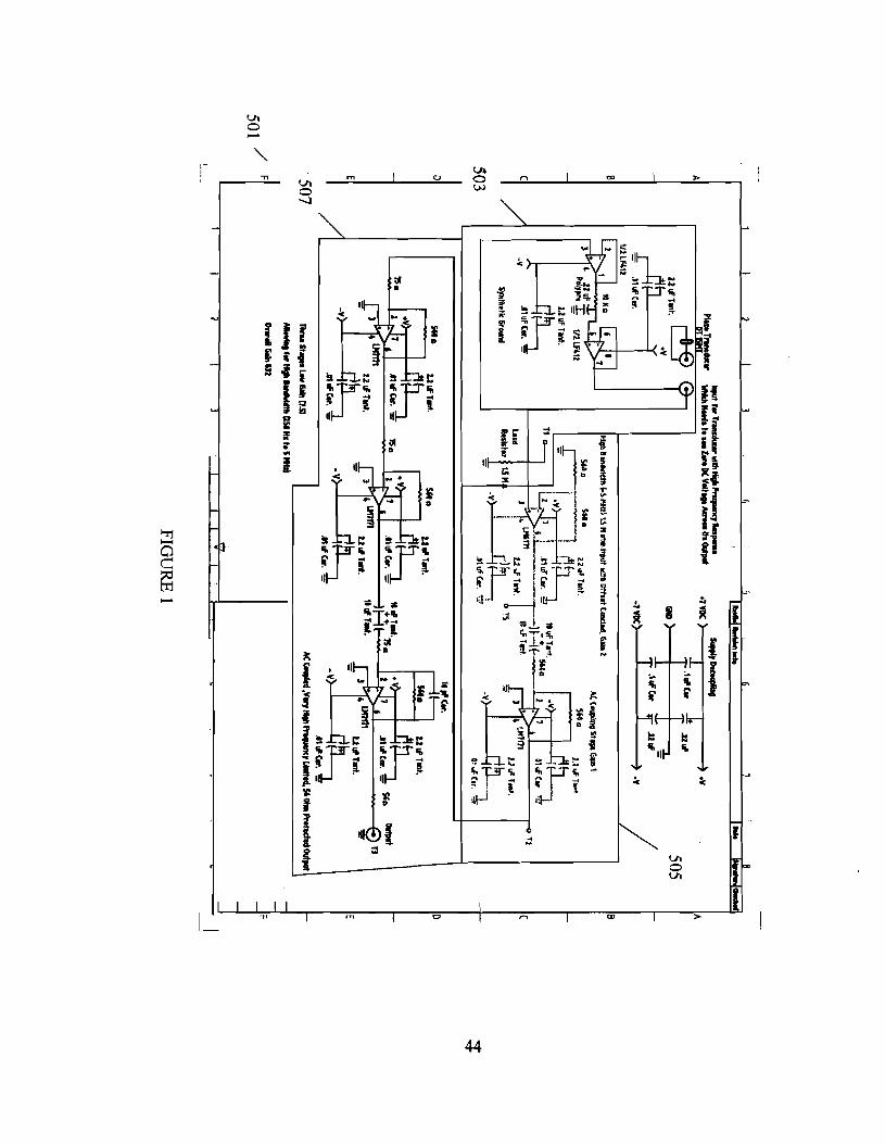
'dl 0 w
- \ -
n I V, n I w I s- I
*
-
.u
'dl u 0 I
0 U 4
A
z f :: sl
S -
r
1 I I I I I r n I CI n m I I Z
- I

1 5,000,000 12 10.108 10.215 10.215 ( Table 1 : The response of the front end of the circuit was
Frequency (Hz) 50
tested and foundto have a flat gain from 50 Hz to 5 m z .
FIGLTRE 2
BK 2
T1 0.1 1
T5 0.22
T2 0.135
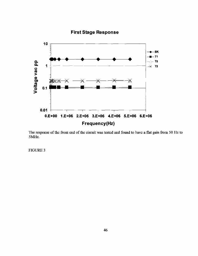
First Stage Response
The response of the fkont end of the circuit was tested and found to have a flat gain fkom 50 Hz to 5MHz.
FIGURE 3

1,000,000 2,000,000 3,000,000 4,000,000 5,000,000
Table 2: The gain of the amplifier as a whole (from T1 to T3) over the frequency range 50 Hz to SMHz, using a signal generator.
0.2 0.2 0.2 0.2 0.2
0.011 0.011 0.011 0.011 0.01 1
7.3 6.65 5.75 4.9 4.1
663.6364 604.5455 522.7273 445.4545 372.7273

Frequency
The gain of the amplifier as a whole (fiom T1 to T3) over the frequency range 50 Hz to SMHz, using a signal generator.
FIGURE 5

Table 3: The gain of the amplifier as a whole (from T1 to T3) over the frequency range 500 Hz to 2.5 MHz, using a piezo "speaker" to drive the detector piezo.

Piezo-driven voltages
The gain of the amplifier as a whole (from T1 to T3) over the frequency range 500 Hz to 2.5 MHz, using a piezo "speaker" to drive the detector piezo.
FIGURE 7

10.4 Po werPoint Presentations The following attached PowerPoint presentations are all related. They were built fi-om the Argonne presentation.
10.4.1 Argonne PowerPoint This presentation was given to the students and facility of IUSB before the Argonne presentation.
Slide 1
Slide 2
OclDbrr 24.2W3 Bldg. 401 Fm Galley Ui 245 pn
A Piezo Transducer For The PICASSO Dark Matter Detector
Ed Behnke Indiana University South Bend
For the Picasso Collaboration
Presentation Funded By an Indiana Uniyemity Souih Bend RBD Committee SMART Grant
Current Work Fine tune our surface mount capability and investigate faster lower noise op-amps. Investigate acoustic coupling response in gel. Develop soflware and hardware solutions to allow determination of bubble location within detector. Develop submergible detector to allow for direct coupling to the gel.
p;c&,*4
Hello, My name is Ed Behnke fi-om Indiana University South Bend. I will talk about the development of an amplifier for the Picasso dark matter detector.
I would like to thank the IUSB R&D committee for funding my talk
The Picasso Collaboration consists of scientists fiom five institutions in the US, Canada and Italy
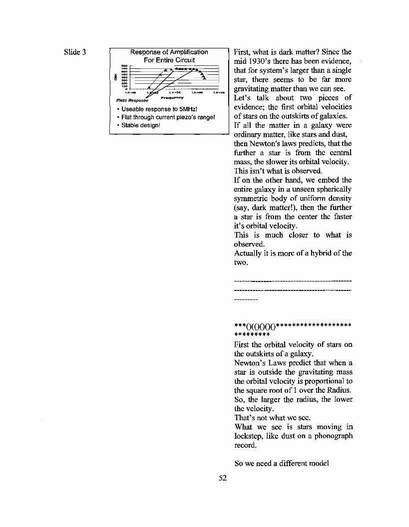
Slide 3 -
Response of Amplification For Entire Circuit
800 700 eon 500 8 :: 100 100
0 1. e
Piezo
Useable response to 5MHz! Flat through current piezo's range! Stable design!
First, what is dark matter? Since the mid 1930's there has been evidence, that for system's larger than a single star, there seems to be far more gravitating matter than we can see. Let's talk about two pieces of evidence; the first orbital velocities of stars on the outskirts of galaxies. If all the matter in a galaxy were ordinary matter, like stars and dust, then Newton's laws predicts, that the further a star is fiom the central mass, the slower its orbital velocity. This isn't what is observed. If on the other hand, we embed the entire galaxy in a unseen spherically symmetric body of uniform density (say, dark matter!), then the further a star is fiom the center the faster it's orbital velocity. This is much closer to what is observed. Actually it is more of a hybrid of the two.
***O(()()()O******************* ********* First the orbital velocity of stars on the outskirts of a galaxy. Newton's Laws predict that when a star is outside the gravitating mass the orbital velocity is proportional to the square root of 1 over the Radius. So, the larger the radius, the lower the velocity. That's not what we see. What we see is stars moving in lockstep, like dust on a phonograph record.
So we need a different model

Slide 8
Slide 9
Piezoelectric Transducers convert ~resrure waves to electric s iana!~ 1
What 1s P~eroelectricity? Permanently palartzed sollds
normally have free charges on thdr surfaces whlch cancel poladzatlon. 4, *.
Sensor - --- -1
~ i i o n i o ~ ~ o r c y d IT rrom Pressure sensitive capacitor- ~ C O U % < ~ C rhmkr)cmncavrptemparan maanet tvDe device " I l l d l - . O&ut p;;pOrtional to size of ' transducer and magnitude of wave.
pressure wave - Can build Piezoelectric - Hi h voltage signals but can't acoustic transducers! delver much power.
Piezoelectric transducers convert pressure waves from acoustic signals into electrical signals. Basically if you bend some types of crystal they create a voltage across the sensor plates If you apply a voltage to the sensor plates it bends the crystal. Its output is mostly voltage and not much current.
The graph is the response of our sensor - sensitivity as a function of frequency. Typical amplifiers take advantage of only a small slice of the frequency. In particular, they use a resonance peak like the one at 150 KHz, and throw all the rest away. Not knowing the frequency content of our bubble, we wish to keep the entire sprectrurn.
The overall detection sequence is as follows: A wimp causes a bubble event. We listen for a bubble, with a piezoelectric acoustic sensor, which converts it to a small electrical signal. We amplifj the signal with the IUSB preamp (see robust signal). We then feed this signal into a digitizer board in our computer.
We believe that our amplifier is unique and IU is in the process of applying for a patent on it.
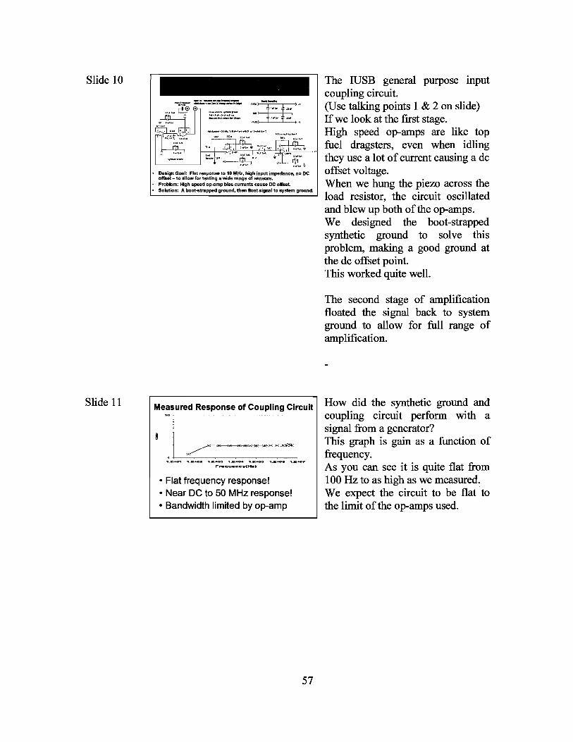
Slide 10
Slide 11
- Design Goal: Flat response to 10 MHz, high input impedance, no DC offset - to allow for testing a vide range of sensora. - Problem: High speed op-amp bias currents cause DC offset - Solution: A bootabapped ground, then float signal to system ground.
Measured Response of Coupling Circuit
m--m---x-)fC~--
* ./- .I =-.I *--I r -a r.e- r e - o s . . ~ - o m q r - o ~
F-gu-nsy("z)
Flat frequency response! Near DC to 50 MHz response! Bandwidth limited by op-amp
The IUSB general purpose input coupling circuit. (Use talking points 1 & 2 on slide) If we look at the first stage. High speed op-amps are like top fuel dragsters, even when idling they use a lot of current causing a dc offset voltage. When we hung the piezo across the load resistor, the circuit oscillated and blew up both of the op-amps. We designed the boot-strapped synthetic ground to solve this problem, making a good ground at the dc offset point. This worked quite well.
The second stage of amplification floated the signal back to system ground to allow for full range of amplification.
How did the synthetic ground and coupling circuit perform with a signal from a generator? This graph is gain as a function of frequency. As you can see it is quite flat from 100 Hz to as high as we measured. We expect the circuit to be flat to the limit of the op-amps used.

Slide 12
Slide 13
Slide 14
Amplification Stage (Standard) Number of hplifisation Stages Due b Slew Rate Limited Bandwidth
Ovcr~ l l systcrn grin about 300 as cornprrd lo 5,000 in standard cireuilr
- Output - plus and minus one volt at system ground. - Slew rates limit maximum anylification per stage . The final stage interfaces to equipment
Response of Amplification For Entire Circuit
Useable response to 5MHz! Flat through current piezo's range! Stable design!
function of time. F r m hentiurn spiked detectors
of same event.
KHz not observed in
This is the main amplification stage. It is built using standard techniques. Because of the robustness of the first stage, our overall system gain is about 300 as compared to 5,000 in standard circuits.
So, how does the entire circuit perform? Again gain as a function of frequency. You can see that we have usable response to about 5 MHz. Our Piezo response is in the flat portion.
How does the circuit perform on real bubble events? The top trace is of the sound wave from a real bubble, amplitude as a function of time (describe) No we aren't seeing wimp's yet, we are using an americium spiked detector to simulate wimps.
The bottom trace is the amplitude as a function of frequency. In particular we see content at 80 and 160 KHz which we don't see in noise events. This should allow us to discriminate noise verses real bubbles.

Slide 15
Slide 16
Preserves all sensor response, allows us to distinguish bubble events vs. noise events1 Lower gain demands!
IUSB to start mapping acoustic properties of detector and various
- Short Term Goals
Catalog bubble event waveforms and frequency content from different sources. Determine attenuation length and sensor angle dependence in water tank. Catalog noise events - generated by known sources. Using two transducers -determine speed of sound in water tank.
piCa4'l
******* We use Americium spiked detectors to simulate Wimp induced bubbles.
Conclusion: (Basically read)
Thanks.
IUSB's short term goals are:
Read the list

Slide 17
Slide 18
Slide 19
Long Term Goals Develop surface mount capability and investigate faster lower noise op-amps. Investigate acoustic coupling response in gel. Develop soflware and hardware solutions to allow determination of bubble location within detector. Develop submergible detector to allow for direct coupling to the gel.
pc'-3b -
Picasso Collaboration Status
- PICASSO shows that the . superheated droplet technique works
-6 detectors with - 60 g active mass installed underground at SNO - clean room facility for production of Inrger modules ready at Montreal
- next step: 1 kg aclive mass by '04
purification work lo reduce alpha- ---mnac\ ,,, background ongoing
envisage 10 kg to 100 kg during 2005 ?.'&$a -
Our Long Term Goals at IUSB are:
Read the list.
Future Goals and present conclusions
Currently 6 one liter detectors are in use. Possible inclusion of Roman lead in detectors Eventual roll out
The Picasso Detector The Dream Detector

Slide 20 DM N t u t r ~ l i b s c a r c h ~ : p m n t ~ +tun
Spin drpndenf
PIC. P.blhle.4 (I@
16nh. UL. LC dbpby
- PIC. IrrnygLTm (In,,
' O = 'm 6m '- .. P..]."dl.lD uumv,s'l
A Novel Piezo Coupling
Ed Behnke Indiana University South Bend
Forthe Picasso Collaboration
Pmsantstion Funded By en Indiana Universiiy South Bend RBD Cornmike
10.4.2 Montreal First Annual Bubble Conference Slide 1 Hello, My name is Ed Behnke ficom
Indiana University South Bend. I will talk about the development of an amplifier for the Picasso dark matter detector.
I would like to thank the IUSB R&D committee for funding my talk

Slide 2
Slide 3 The PICASSO Detection Technique IUSB IS re~pons~bls for the RSD ofthe acoumc proplbas, and radlmssay technques
Piaaelectric acoustic sensor mrns \ nconstic wave into tiny rlretrieul
IUSB Piezo amplifier OscRlacope md.Dr
Acoustic shock waves from phase transition
The overall real time detection sequence is as follows: A wimp interaction causes phase transition or a bubble event with about one half the energy in the ultrasound signal. The picasso experiment uses ultrasonic sensors (currently externally mounted piezoelectric transducers) to detect this signal TUSB is responsible for studying the acoustic properties of the detector fiom the generation of the bubble to the point where I The electronic signal leaves the transducer. (including understanding the speed of sound, angular dependence of emcienmcy attenuation, etc.)
In order to accomplish this the first step in our program was to develop a preamplifier with little filtering of the signal and with a gain which was unifiom over a wide range of hquencies. I will describe the problems in reading the transducer in an unbiased fashion and how we have solved this
We listen with a piezoelectric acoustic transducer, which converts
62

Slide 4
the acoustic signal into a small electrical signal. We amplify the signal with a broadband preamp. We then feed this signal into a digitizer board in our computer for storage and eventual offline analysis.
We believe that our amplifier is novel, as we have been unable to find other similar implementations and that it solves the interface problem to the piezo electric transducer.
Piezoelectric Transducers convert pressure waves to electric signals
I Piezoelectric transducers convert What is Piezoelectricity? a
Permanenlly polarized solids - pressure waves from acoustic signals into electrical signals. Basically if you bend some types of crystal they create a voltage across the sensor plates If you apply a voltage to the sensor plates it bends the crystal. Its output is mostly voltage and not much current.
The graph is the response of our sensor - sensitivity as a function of fiequenc y . Typical amplifiers take advantage of only a small slice of the frequency. In particular, they use a resonance peak like the one at 150 KHz, and throw all the rest away. Not knowing the frequency content of our bubble, we wish to keep the entire sprectrum.

Slide 5
Slide 6
- Design Goal: Flat response to 10 MHz, high input impedance, no DC offset - to allow for testing a rride range of sensors. Problem: Huh speed op-amp bias cunent.5 cause DC offset. Solution: A bootabapped ground, men float signal to system ground.
The IUSB general purpose input coupling circuit. (Use talking points 1 & 2 on slide) If we look at the first stage. High speed op-amps are like top fuel dragsters, even when idling they use a lot of current causing a dc offset voltage. When we hung the piezo across the load resistor, the circuit oscillated and blew up both of the op-amps. We designed the boot-strapped synthetic ground to solve this problem, making a good ground at the dc offset point. This worked quite well.
Measured Response of Coupling Circuit
The second stage of amplification floated the signal back to system ground to allow for full range of amplification.
b l o l , , , , ,
x-x- x *--x-x--& A-
How did the synthetic ground and coupling circuit perform with a signal from a generator? This graph is gain as a function of frequency. As you can see it is quite flat from 100 Hz to as high as we measured. We expect the circuit to be flat to the limit of the op-amps used.
, I _ e r O l l . m r 0 1 r . e m l r . e m 4 -.ems - . e m - - . E m 7
,=rrqurnsyc-,
Flat frequency response! Near DC to 50 MHz response! Bandwidth limited by op-amp
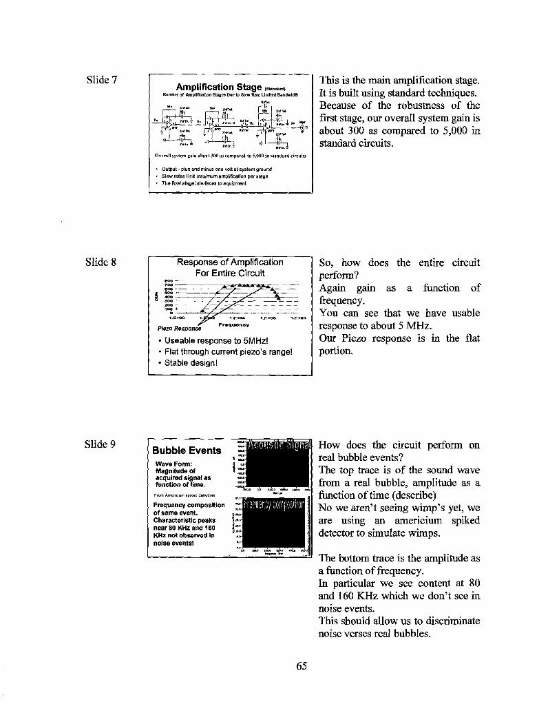
Slide 8
Slide 9
Amplification Stage (Smnad, Number of I\mplifiwUon Stages Dueto Slev Rab LimltedBandwidth
n*k =
Ovcrall syacm sin nbout 300 us camgrrd to 5,000 in slandanl circuits
. Output - plus and minus one volt at system gmund. Slew rabs limit maximumarrplificalion per stage . The final stage interfaces to equipment
Response of Amplification For Entire Circuit
-0-3 700
800 5.30
8 2: 200
100 0
1.
Piezo Response F-uency
Useable response to SMHz! Flat through current piezo's range! Stable design!
This is the main amplification stage. It is built using standard techniques. Because of the robustness of the first stage, our overall system gain is about 300 as compared to 5,000 in standard circuits.
So, how does the entire circuit perform? Again gain as a function of fkequenc y. You can see that we have usable response to about 5 MHz. Our Piezo response is in the flat portion.
How does the circuit perform on real bubble events? The top trace is of the sound wave
acquired signal as function of time. fkom a real bubble, amplitude as a Frm henuurn hplkpd detectors function of time (describe) Frequency composition 2 of same event. No we aren't seeing wimp's yet, we Characteristic peaks 12 are using an americium spiked near 80 KHz and 160 1: KHZ not observed in detector to simulate wimps.
The bottom trace is the amplitude as a function of frequency. In particular we see content at 80 and 160 KHz which we don't see in noise events. This should allow us to discriminate noise verses real bubbles.
Slide 7

Slide 10
Slide 11
Current Work
Catalog bubble event waveforms and frequency content from different sources. Determine attenuation length and sensor angle dependence in water tank. Catalog noise events - generated by known sources. Using two transducers - determine speed of sound in water tank.
Current Work Develop surface mount capability and investigate faster lower noise op-amps. Investigate acoustic coupling response in gel. Develop software and hardware solutions to allow determination of bubble location within detector. Develop submergible detector to allow for direct coupling to the gel.
, T - ' r ' h ~ b - ..
******* We use Americium spiked detectors to simulate Wimp induced bubbles.
WSB's short term goals are:
Read the list
Our Long Term Goals at WSB are:
Read the list.

Slide 12
Slide 13
IUSB circuit is unique and has- been submitted for patenting! Preserves all sensor response, allows us to distinguish bubble events vs. noise events! Lower gain demands!
IUSB to start mapping acoustic properties of detector and various
Conclusion: (Basically read)
Thanks.
10.4.3 Spring APS Powerpoint This presentation was given to the students and faculty of IUSB before the spring meeting.

Slide 1
Slide 2
Slide 3
MeeUng - Denver
An Innovative Piezoelectric Sensor Preamplifier for the Picasso Dark Matter
Detector
Edward Behnke Indiana University South Bend
Forthe Picasso Collaboration
Hello, My name is Ed Behnke fiom Indiana University South Bend. I will talk about the development of a preamplifier amplifier for the Picasso dark matter detector.
The p=b Collaboration I
The PICASSO Detection Technique IUSB ir reswnuble far the RBD d Ihe acoustic propemes, and radioassay technique6
Pie2aelmtric acoustic sensor hlms \ amustic wave inlo tiny clcctricrl
Acoustic shock waves from phase IransiUon
The Picasso Collaboration consists of scientists fiom five institutions in the US, Canada and Italy
This is the starting point
I will discuss the piezo and the electronic fiont end

Slide 4 I Piezoelectric Transducers convert pressure waves to electric signals I
What is Piezoelectricity? a
Permanently polarized solids normally have free charges on melr surla- which cancel polartralion. ,,
Sensor + , - Plate0 ?-"
+( !J~,(:J~ PI> I U s ~ mmEe+d.Yhm.LYOUn - .
~ ~ n o r n o o l ofryslal (V rrom Pressure sensitive capacitor- ~nrvvstir shucks)cmnravu empormr). magnet type device
; " ~ p o ' ' ~ , " ~ ; ~ , " ' a o d . Output proportional to size of
~ w v c o m p iti onor, bbbk transducer and magnitude of
-a,=. pressure wave
--r Can build Piezoelectric - Hi h voltage signals but can't acoustic transducers! delver much power.
A piezoelectric transducers converts pressure waves from the bubble induced acoustic signals from the detector into electrical signals.
Piezoelectric transducers work by converting mechanical energy into an electrical signal. Basically if you bend the crystal it generates a voltage across its sensor plates. Conversly, if you apply a voltage to the sensor plates, this generates a mechanical deformation in the crystal. A piezoelectric crystal of the size we use mostly generates voltage and not much current. Since the crystal is not a good conductor its quiesent response is ill defined (it doesn't tie
-
the input to system ground when no signal is present.
The graph is the response of the current picasso sensor - sensitivity as a function of frequency.
Typical coupling circuits take advantage of only a small slice of the frequency bandwidth of the transducer.. In particular coupling amplifiers commonaly use a resonance peak like the one at 150 KHz, and throw the remaining signal away.
Since we are studying the frequency content of our bubble generated signal, we want to keep the entire sprectrum, as linearly as possible.

Slide 5 This is the IUSB general purpose input coupling circuit.
-2- zzzrEmw---~z .,- ;-) .. I ,,,,, z? *_,>?" .,,..". % 11.- f=.* 1 & ?&f LT:=:,,-
7.x)
Id* 7 =* ) (Use talking points 1 & 2 on slide)
Design Goal: Flat response to 10 MHz, high input impedance, no DC offset- to allow for testing a wide range of sensors. - Problem: High speed opqmp bias currents cause DC o f k t - Solution: A bootatrapped ground, men float signal to system ground.
Specifically the quiescent current which is in the order micro amps for a standard speed transistor op amp. It small fiaction of that for JFE
bias of 2 high is a
T OP amps, but the ones we found have significant phase shift as a function of frequency and a reduced usable bandwidth.
If we look at the first stage, we are tying the input to ground with a fixed 1 M resistor. This multiplied by the quiescent bias current gives an offset of a couple volts.
When we attached the piezo across the load resistor, the circuit oscillated severely and blew the op- amps.
To rectifl this condition we designed the boot-strapped synthetic ground. This worked, stopping all oscillation, making a good ground at the dc offset point. This worked quite well.
The second stage of amplification floated the signal back to system ground to allow for full range of amplification.

Slide 6
Slide 7
Slide 8
Measured Response of Coupling Circuit
, , , , , 1 /--x- X--- ~ ~ r n r n - X - ~
.l_e-o1 *.--or r.=-oa .=-or ..--as r.e-aa r.e-o7
Fr-qu-nsy#-,
Flat frequency response! Near DC to 50 MHz response! Bandwidth limited by op-amp
Amplification Stage (Standard) Nurnkr of Amplification Stag- Due to Slew Rate Limited Bsndwldth
Ovcmll system gain abont 300 as comparcd to 5,000 in standard circuits
- Output - plus and minus one volt at system ground. - Slew rates limit rraximum amplification per stage The final stage interfaces to equipment
Response of Amplification For Entire Circuit
Useable response to 5MHz! Flat through current piezo's range! Stable design!
How did the synthetic ground and coupling circuit perform with a signal fiom a generator? This graph is gain as a function of fiequenc y . As you can see it is quite flat from 100 Hz to as high as we measured. We expect the circuit to be flat to the limit of the op-amps used.
This is the main amplification stage. It is built using standard techniques. Because of the robustness of the first stage, our overall system gain is about 300 as compared to 5,000 in standard circuits.
So, how does the entire circuit perform? Again gain as a function of fiequency. You can see that we have usable response to about 5 MHz. Our Piezo response is in the flat portion.

Slide 9
Slide 10 New IUSB Transducer
..l.bn
How does the circuit perform on real bubble events? The top trace is of the sound wave fiom a real bubble, amplitude as a function of time (describe) No we aren't seeing wimp's yet, we are using an americium spiked detector to simulate wimps.
The bottom trace is the amplitude as a function of frequency. In particular we see content at 80 and 160 KHz which we don't see in noise events. This should allow us to discriminate noise verses real bubbles.
******* We use Americium spiked detectors to simulate Wimp induced bubbles.
This is the output of the head circuit. This has the new higher bandwidth op amps which are low noise.
The red is the first amplifier signal with no piezo attached. The second is the output of the head with a standard piezo attached and triggered with a tap.
You can see that there is not much noise. We are still working on this portion of the circuit and will increase its gain. Primarily it looks like it will stay very quiet.

Slide 1 1
Slide 12
Slide 13
Current Work
Finish the electronics and develop custom piezoelectric transducers. Study attenuation length and sensor angle dependence in water tank. Catalog events - generated by known sources. Using two transducers -determine speed of sound in water tank.
, P r ' ~ b b -
Current Work
Fine tune our surface mount capability and investigate faster lower noise op-amps. Investigate acoustic coupling response in gel. Develop soflware and hardware solutions to allow determination of bubble location within detector. Develop submergible detector to allow for direct coupling to the gel.
P i C s b b d
Our design preserves sensor
Appears t o allow us t o distinguish bubble events vs. noise events! Lower gain demands!
IUSB to start mapping acoustic
IUSB's short term goals are:
Read the list
Our Long Term Goals at IUSB are:
Read the list.
Conclusion: (Basically read)
Thanks.


I I References
[l] Connecting Quarks With the Cosmos: Eleven Science Questions for the New Century, committee on the Physics of the Universe, National Research Council of the National Academies, National Academic Press, 2003
[2] F. Zwicky, Helv. Phys. Acta 6, 1 10, F. Zwicky, Astrophysical Journal, vol. 86, p.2 17, 1937.
[3] S. Shore, The Tapestry of Modern Astrophysics, John Wiley & Sons, Inc., 2003, ISBN 0-471- 16816-5(S. Shore, now at the University of Pisa, is a PICASSO collaborator.)
[4] Lewis, Aaron D.; Buote, David A.; Stocke, John T. 2003, ApJ, 586,135 (Abell 2029 but a good paper to reference for dark matter halos) the observations, in X-rays, of the galaxy cluster Abell 2029 http://www.msfc.nasa.gov/news/photos/photoaallerlv/chandra/chana5.html or ROSAT http://apod.gsfc.nasa.(zov/apod~ap990404.html. D. Laurence et al., The Astrophysical Journal, vol. 428, no. 2, pt. 1, p. 544-554
P I Such as the lensing by Abell 2218: http:lkubblesite.orgldiscoveries/l Oth~photos/~aphics/slide36med.ipg and http://~wst.gsfc.nasa.aov/science/mavlens.htm
[6]C. Alcock, et a1 (The MACHO Collaboration) ApJ, 471,774 (1996)
[7] B. Bernadis et al., BOMERANG Coll., Nature 404 (2000) 955, Abroe, M.E. et al, (MAXIMA) "Correlations Between the WMAP and MAXIMA Cosmic Microwave Background Anisotropy Maps," 2003. Submitted to ApJ. astro-phl0308355, C.L. Bennet et al.,(WMAP) ApJS 138, 1 and D.N. Spergel et. al., (WMAP) ApJS, 148, 175 (cosmological parameters fiom WMAP)astro- ph10202209.
[8]A. Bottino et al., Phys. Lett. B295 (1992)330
[9] ANUS, CASPAR, CDMS, CRESST, CUORE , DAMA, DRIFT, EDELWEISS, GENIUS, HDMS, IGEX, LIBRA, MACHe3, MAJORANA, NAIAD, ORPHEUS, PICASSO, ROSEBUD, UKDMC, ZEPLIN.
[10]The PICASSO eroject In -da to Search for Supersymmetric Objects) collaboration:
M. Di Marco, P. Doane, M.H. Genest, R. Gornea, M. BernabC-Heider, C. Leroy, L. Lessard, J.P. Martin, U. Wichoski, V. Zacek, Universite de Montreal, Montreal. OB, Canada.
A.J. Noble, Queens University, Kingston, ON, Canada.
E. Behnke, J. Behnke, W. Feighery, I. Levine, C. Muthusi, J. Neurenberg, R. Nyrnberg, Indiana University South Bend, IN, USA.
75