design of high-bandwidth and high-linearity input buffers
TRANSCRIPT

David Barros Leonardo
Licenciatura em Ciências da Engenharia Electrotécnica e de Computadores
Design of High-Bandwidth and High-LinearityInput Buffers for ADCs
Dissertation submitted in partial fulfillmentof the requirements for the degree of
Master of Science inEngenharia Electrotécnica e de Computadores
Adviser: João Carlos da Palma Goes,Prof. Doutor, NOVA University of Lisbon
Examination Committee
Chairperson: André MoraRaporteur: Luís Bica Oliveira
November, 2020


Design of High-Bandwidth and High-Linearity Input Buffers for ADCs
Copyright © David Barros Leonardo, Faculty of Sciences and Technology, NOVA Univer-
sity Lisbon.
The Faculty of Sciences and Technology and the NOVA University Lisbon have the right,
perpetual and without geographical boundaries, to file and publish this dissertation
through printed copies reproduced on paper or on digital form, or by any other means
known or that may be invented, and to disseminate through scientific repositories and
admit its copying and distribution for non-commercial, educational or research purposes,
as long as credit is given to the author and editor.
This document was created using the (pdf)LATEX processor, based in the “novathesis” template[1], developed at the Dep. Informática of FCT-NOVA [2].[1] https://github.com/joaomlourenco/novathesis [2] http://www.di.fct.unl.pt


Acknowledgements
I would like to thank all the professors who were part of my academic path and who were
kind enough to share some of their knowledge with me. I would like to give a special
thanks to Professor Luís Oliveira for all the help given at the beginning of my master’s
degree and a huge thanks to Professor João Goes for having accepted to advise and to
have advised me in this work.
I am thanking the people at Xilinx Ireland for the opportunity of an internship while
working at my thesis. Special thanks to Vincent Callaghan, Bruno Vaz, Roswald Francis
and Sohaib Afridi for their patience and will to teach me all of the important things for
for my work there.
I will not forget my peers, friends and colleagues and their dedication, I would like to
thank everyone who made me the person I am today. I would like to give special thanks
to Francisco Matos, Diogo Pereira, Lucas Fioravanço and Clarisse Feio for all the support
they gave me during my years in college and a special word for Miguel Calado for keeping
my spirits high in the last stage of the thesis.
Finally, I would like to thank my parents, for all the work, effort and dedication that
they have shown in all these years, and my little sister, for always being concerned with
things that would never bother me.
v


Abstract
Nowadays on-chip Input Buffers (IBs) for direct conversion front-ends are realized
with a higher voltage supply than that of the core voltage of the technology, mainly for
linearity purposes. This, in turn, makes it mandatory to have more than one voltage
source to supply a single chip in addition to having devices capable of handling higher
voltages.
This work explores the possibility of having IBs supplied with the technology’s core
voltage to standardize all of the devices and reducing the different voltage supply sources
and/or voltage regulators needed for operating the front-end drivers of the Analog to
Digital Converters (ADCs).
A new input buffer architecture will be presented and compared to some prior input
buffer implementations in the same conditions. This new architecture presents good
linearity and bandwidth results and can be used for input buffers with the added benefit
of not needing higher voltages nor special devices.
This new architecture is based off an existing one with another feedback loop to
improved high-frequency peaking and linearity issues. This architecture achieves better
results in bandwidth, a SNDR of 58 dB with and output voltage of 600 mV peak-to-peak
differential. Furthermore, this buffer achieves a better efficiency linearity-wise when
comparing to other buffers in the same conditions.
Keywords: ADC, Input Buffer, CMOS, High Linearity, High Bandwidth, Direct Conver-
sion, Harmonic Distortion, Intermodulation Distortion.
vii


Resumo
Nos dias que correm, Input Buffers (IBs) para interfaces de alta frequência dos circui-
tos de conversão directa em receptores de áudio são alimentados com tensões superiores à
tensão de alimentação nominal da tecnologia, principalmente por questões de linearidade.
Isto obriga ao uso de várias fontes de tensão para alimentar um único chip bem como a
utilização de transístores capazes de suportar maiores níveis de tensão.
Neste trabalho é explorada a possibilidade de usar IBs com tensão de alimentação no-
minal para uniformizar todos os transístores utilizados dentro de um projecto e diminuir
a necessidade de mais do que um nível de tensão para a operação dos drivers dos Analog
to Digital Converters (ADCs).
Será apresentada uma nova arquitectura e esta será comparada, nas mesmas condições,
com várias implementações de input buffer existentes na literatura. Esta nova arquitec-
tura apresenta bons resultados em termos de linearidade e largura de banda, podendo
ser utilizada para projectos de alta frequência sem a necessidade de diferentes tipos de
dispositivos ou diferentes níveis de tensão.
Esta nova arquitectura é baseada noutra acrescentando uma malha de realimentação
para melhorar a linearidade e peakings na largura de banda a altas frequências. Esta
arquitectura tem melhores resultados em termos de largura de banda, um SNDR de 58
dB com um sinal de saída com 600 mV pico-a-pico diferencial. Para além disto, este
buffer é mais eficiente em termos de linearidade quando comparado com outros buffers
nas mesmas condições.
Palavras-chave: ADC, Input Buffer, CMOS, Linearidade, Largura de Banda, Converão
Directa, Distorção Harmónica, Distorção de Intemodulação.
ix


Contents
List of Figures xv
List of Tables xvii
Acronyms xix
1 Introduction 1
1.1 Motivation and Background . . . . . . . . . . . . . . . . . . . . . . . . . . 1
1.2 Objectives and Original Contribution . . . . . . . . . . . . . . . . . . . . . 4
1.3 Thesis Organization . . . . . . . . . . . . . . . . . . . . . . . . . . . . . . . 5
2 review of state-of-the-art 7
2.1 General Purpose Buffers . . . . . . . . . . . . . . . . . . . . . . . . . . . . 8
2.1.1 Common Drain Input Buffer . . . . . . . . . . . . . . . . . . . . . . 8
2.1.2 Cascaded Source Follower Input Buffer . . . . . . . . . . . . . . . . 11
2.1.3 Super Source Follower Input Buffer . . . . . . . . . . . . . . . . . . 12
2.1.4 Flipped Voltage Follower Input Buffer . . . . . . . . . . . . . . . . 13
2.2 Input Buffers Design . . . . . . . . . . . . . . . . . . . . . . . . . . . . . . 13
2.2.1 Differential Source Follower Input Buffer . . . . . . . . . . . . . . 13
2.2.2 Differential Super Source Follower Input Buffer . . . . . . . . . . . 14
2.2.3 Input Buffer with Current Feedback . . . . . . . . . . . . . . . . . 15
2.2.4 Push-Pull Input Buffer . . . . . . . . . . . . . . . . . . . . . . . . . 16
2.2.5 Vgs-controlled Cascaded Source Follower Input Buffer . . . . . . . 17
2.3 Other implementations . . . . . . . . . . . . . . . . . . . . . . . . . . . . . 18
2.3.1 BiCMOS solution . . . . . . . . . . . . . . . . . . . . . . . . . . . . 18
2.4 Final thoughts . . . . . . . . . . . . . . . . . . . . . . . . . . . . . . . . . . 19
3 Study and simulation of the voltage buffers 21
3.1 The Process Guidelines and Simulating Conditions . . . . . . . . . . . . . 21
3.2 Sizing . . . . . . . . . . . . . . . . . . . . . . . . . . . . . . . . . . . . . . . 22
3.2.1 Sizing Main Buffer Transistors . . . . . . . . . . . . . . . . . . . . . 22
3.2.2 Sizing Current Biasing Circuitry . . . . . . . . . . . . . . . . . . . 23
3.2.3 Sizing Feedback . . . . . . . . . . . . . . . . . . . . . . . . . . . . . 24
xi

CONTENTS
3.3 Simulation testbench . . . . . . . . . . . . . . . . . . . . . . . . . . . . . . 25
3.4 Simulations setup and objectives . . . . . . . . . . . . . . . . . . . . . . . 26
3.4.1 DC Simulation . . . . . . . . . . . . . . . . . . . . . . . . . . . . . . 27
3.4.2 AC Simulation . . . . . . . . . . . . . . . . . . . . . . . . . . . . . . 27
3.4.3 Transient-noise Simulation . . . . . . . . . . . . . . . . . . . . . . . 27
4 Analysis and Results of the state-of-the-art 29
4.1 Source Follower Input Buffer Analysis . . . . . . . . . . . . . . . . . . . . 29
4.1.1 DC Analysis (SF) . . . . . . . . . . . . . . . . . . . . . . . . . . . . 29
4.1.2 AC Analysis (SF) . . . . . . . . . . . . . . . . . . . . . . . . . . . . 30
4.1.3 Transient-noise Analysis (SF) . . . . . . . . . . . . . . . . . . . . . 31
4.2 Super Source Follower Input Buffer Analysis . . . . . . . . . . . . . . . . . 33
4.2.1 DC Analysis (SSF) . . . . . . . . . . . . . . . . . . . . . . . . . . . . 33
4.2.2 AC Analysis (SSF) . . . . . . . . . . . . . . . . . . . . . . . . . . . . 33
4.2.3 Transient-noise Analysis (SSF) . . . . . . . . . . . . . . . . . . . . . 34
4.3 Cascaded Source Follower Input Buffer Analysis . . . . . . . . . . . . . . 36
4.3.1 DC Analysis (CSF) . . . . . . . . . . . . . . . . . . . . . . . . . . . 36
4.3.2 AC Analysis (CSF) . . . . . . . . . . . . . . . . . . . . . . . . . . . . 37
4.3.3 Transient-noise Analysis (CSF) . . . . . . . . . . . . . . . . . . . . 37
4.4 Current Feedback Input Buffer Analysis . . . . . . . . . . . . . . . . . . . 39
4.4.1 DC Analysis (Current Feedback Input Buffer (Current Feedback IB)) 39
4.4.2 AC Analysis (Current Feedback IB) . . . . . . . . . . . . . . . . . . 40
4.4.3 Transient-noise Analysis (Current Feedback IB) . . . . . . . . . . . 41
4.5 Vgs-controlled Cascaded Source Follower Input Buffer . . . . . . . . . . . 43
4.5.1 DC Analysis (Vgs-controlled Cascaded Source Follower (CSF) Input
Buffer (IB)) . . . . . . . . . . . . . . . . . . . . . . . . . . . . . . . . 43
4.5.2 AC Analysis (Vgs-controlled CSF IB) . . . . . . . . . . . . . . . . . 43
4.5.3 Transient-noise Analysis (Vgs-controlled CSF IB) . . . . . . . . . . 44
4.6 Summary of all the analyses . . . . . . . . . . . . . . . . . . . . . . . . . . 46
5 Proposed Architecture 49
5.1 Circuit Schematic and Proposed Idea . . . . . . . . . . . . . . . . . . . . . 49
5.2 DC Analysis . . . . . . . . . . . . . . . . . . . . . . . . . . . . . . . . . . . 50
5.3 AC Analysis . . . . . . . . . . . . . . . . . . . . . . . . . . . . . . . . . . . 51
5.4 Transient-noise Analysis . . . . . . . . . . . . . . . . . . . . . . . . . . . . 53
5.5 Proposed Buffer with Improvements . . . . . . . . . . . . . . . . . . . . . 56
5.5.1 DC Analysis . . . . . . . . . . . . . . . . . . . . . . . . . . . . . . . 57
5.5.2 AC Analysis . . . . . . . . . . . . . . . . . . . . . . . . . . . . . . . 58
5.5.3 Transient-noise Analysis . . . . . . . . . . . . . . . . . . . . . . . . 59
6 Conclusion 65
6.1 Final Comparisons . . . . . . . . . . . . . . . . . . . . . . . . . . . . . . . . 65
xii

CONTENTS
6.2 Final conclusion of the work . . . . . . . . . . . . . . . . . . . . . . . . . . 68
Bibliography 69
xiii


List of Figures
1.1 High level design of a direct-conversion Receiver System (Rx) comprising an
IB and an ADC. . . . . . . . . . . . . . . . . . . . . . . . . . . . . . . . . . . . 2
1.2 High level representation (a) and implementation (b) of a buffer. . . . . . . . 3
1.3 Basic common-drain topology [12]. . . . . . . . . . . . . . . . . . . . . . . . . 3
2.1 Source Follower Design. . . . . . . . . . . . . . . . . . . . . . . . . . . . . . . 9
2.2 Small-Signal equivalent with Ideal Current Source (no parasitic effects, no
body effect.) . . . . . . . . . . . . . . . . . . . . . . . . . . . . . . . . . . . . . 9
2.3 Cascaded Source Follower Design. . . . . . . . . . . . . . . . . . . . . . . . . 11
2.4 Super Source Follower. . . . . . . . . . . . . . . . . . . . . . . . . . . . . . . . 12
2.5 Flipped Voltage Follower [20]. . . . . . . . . . . . . . . . . . . . . . . . . . . . 13
2.6 Differential Source Follower IB [16]. . . . . . . . . . . . . . . . . . . . . . . . 14
2.7 Differential Super Source Follower IB [16]. . . . . . . . . . . . . . . . . . . . . 15
2.8 Current Feedback Input Buffer. . . . . . . . . . . . . . . . . . . . . . . . . . . 16
2.9 Push-Pull Input Buffer [14]. . . . . . . . . . . . . . . . . . . . . . . . . . . . . 17
2.10 Cascaded Source Follower with Vgs control [26]. . . . . . . . . . . . . . . . . 18
2.11 BiCMOS PMOS input buffer [6]. . . . . . . . . . . . . . . . . . . . . . . . . . . 19
3.1 Source Follower. . . . . . . . . . . . . . . . . . . . . . . . . . . . . . . . . . . . 22
3.2 Current Feedback buffer (Current Mirror Feedback Highlighted). . . . . . . . 24
3.3 Simulation testbench for all the simulated buffers. . . . . . . . . . . . . . . . 25
3.4 Current Mirror used to BIAS all the simulated circuits. . . . . . . . . . . . . . 26
4.1 Source Follower DC Operating point. . . . . . . . . . . . . . . . . . . . . . . . 30
4.2 Source Follower Frequency Response. . . . . . . . . . . . . . . . . . . . . . . . 30
4.3 Source Follower Output (time). . . . . . . . . . . . . . . . . . . . . . . . . . . 31
4.4 Source Follower Output (frequency). . . . . . . . . . . . . . . . . . . . . . . . 31
4.5 Source Follower 2 Tone Analysis Output (time). . . . . . . . . . . . . . . . . . 32
4.6 Source Follower 2 Tone Analysis Output (frequency). . . . . . . . . . . . . . . 32
4.7 Super Source Follower DC Operating point. . . . . . . . . . . . . . . . . . . . 33
4.8 Super Source Follower Frequency Response. . . . . . . . . . . . . . . . . . . . 34
4.9 Super Source Follower Output (time). . . . . . . . . . . . . . . . . . . . . . . . 34
4.10 Super Source Follower Output (frequency). . . . . . . . . . . . . . . . . . . . 35
xv
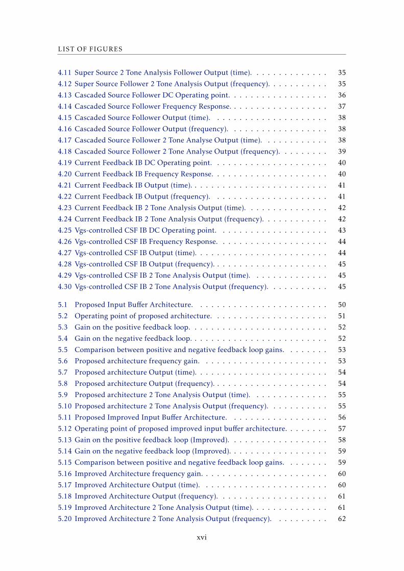
LIST OF FIGURES
4.11 Super Source 2 Tone Analysis Follower Output (time). . . . . . . . . . . . . . 35
4.12 Super Source Follower 2 Tone Analysis Output (frequency). . . . . . . . . . . 35
4.13 Cascaded Source Follower DC Operating point. . . . . . . . . . . . . . . . . . 36
4.14 Cascaded Source Follower Frequency Response. . . . . . . . . . . . . . . . . . 37
4.15 Cascaded Source Follower Output (time). . . . . . . . . . . . . . . . . . . . . 38
4.16 Cascaded Source Follower Output (frequency). . . . . . . . . . . . . . . . . . 38
4.17 Cascaded Source Follower 2 Tone Analyse Output (time). . . . . . . . . . . . 38
4.18 Cascaded Source Follower 2 Tone Analyse Output (frequency). . . . . . . . . 39
4.19 Current Feedback IB DC Operating point. . . . . . . . . . . . . . . . . . . . . 40
4.20 Current Feedback IB Frequency Response. . . . . . . . . . . . . . . . . . . . . 40
4.21 Current Feedback IB Output (time). . . . . . . . . . . . . . . . . . . . . . . . . 41
4.22 Current Feedback IB Output (frequency). . . . . . . . . . . . . . . . . . . . . 41
4.23 Current Feedback IB 2 Tone Analysis Output (time). . . . . . . . . . . . . . . 42
4.24 Current Feedback IB 2 Tone Analysis Output (frequency). . . . . . . . . . . . 42
4.25 Vgs-controlled CSF IB DC Operating point. . . . . . . . . . . . . . . . . . . . 43
4.26 Vgs-controlled CSF IB Frequency Response. . . . . . . . . . . . . . . . . . . . 44
4.27 Vgs-controlled CSF IB Output (time). . . . . . . . . . . . . . . . . . . . . . . . 44
4.28 Vgs-controlled CSF IB Output (frequency). . . . . . . . . . . . . . . . . . . . . 45
4.29 Vgs-controlled CSF IB 2 Tone Analysis Output (time). . . . . . . . . . . . . . 45
4.30 Vgs-controlled CSF IB 2 Tone Analysis Output (frequency). . . . . . . . . . . 45
5.1 Proposed Input Buffer Architecture. . . . . . . . . . . . . . . . . . . . . . . . 50
5.2 Operating point of proposed architecture. . . . . . . . . . . . . . . . . . . . . 51
5.3 Gain on the positive feedback loop. . . . . . . . . . . . . . . . . . . . . . . . . 52
5.4 Gain on the negative feedback loop. . . . . . . . . . . . . . . . . . . . . . . . . 52
5.5 Comparison between positive and negative feedback loop gains. . . . . . . . 53
5.6 Proposed architecture frequency gain. . . . . . . . . . . . . . . . . . . . . . . 53
5.7 Proposed architecture Output (time). . . . . . . . . . . . . . . . . . . . . . . . 54
5.8 Proposed architecture Output (frequency). . . . . . . . . . . . . . . . . . . . . 54
5.9 Proposed architecture 2 Tone Analysis Output (time). . . . . . . . . . . . . . 55
5.10 Proposed architecture 2 Tone Analysis Output (frequency). . . . . . . . . . . 55
5.11 Proposed Improved Input Buffer Architecture. . . . . . . . . . . . . . . . . . 56
5.12 Operating point of proposed improved input buffer architecture. . . . . . . . 57
5.13 Gain on the positive feedback loop (Improved). . . . . . . . . . . . . . . . . . 58
5.14 Gain on the negative feedback loop (Improved). . . . . . . . . . . . . . . . . . 59
5.15 Comparison between positive and negative feedback loop gains. . . . . . . . 59
5.16 Improved Architecture frequency gain. . . . . . . . . . . . . . . . . . . . . . . 60
5.17 Improved Architecture Output (time). . . . . . . . . . . . . . . . . . . . . . . 60
5.18 Improved Architecture Output (frequency). . . . . . . . . . . . . . . . . . . . 61
5.19 Improved Architecture 2 Tone Analysis Output (time). . . . . . . . . . . . . . 61
5.20 Improved Architecture 2 Tone Analysis Output (frequency). . . . . . . . . . 62
xvi

List of Tables
3.1 Specifications of the simulation. . . . . . . . . . . . . . . . . . . . . . . . . . . 21
3.2 Buffer Transistors Sizing. . . . . . . . . . . . . . . . . . . . . . . . . . . . . . . 23
3.3 Current Sources Sizing. . . . . . . . . . . . . . . . . . . . . . . . . . . . . . . . 24
4.1 Summary from the Source Follower Simulation Analysis. . . . . . . . . . . . 32
4.2 Summary from the Super Source Follower Simulation Analysis. . . . . . . . . 35
4.3 Summary from the Cascaded Source Follower Simulation Analysis. . . . . . 39
4.4 Summary from the Current Feedback IB Simulation Analysis. . . . . . . . . . 42
4.5 Summary from the Vgs-controlled CSF IB Simulation Analysis. . . . . . . . . 45
4.6 Comparison between tested designs analysis. . . . . . . . . . . . . . . . . . . 46
5.1 Summary from the Proposed Buffer Simulation Analysis. . . . . . . . . . . . 55
5.2 Summary from the Improved Buffer Simulation Analysis. . . . . . . . . . . . 61
5.3 Comparison between simulated designs analysis. . . . . . . . . . . . . . . . . 62
6.1 Comparison between tested designs analysis. . . . . . . . . . . . . . . . . . . 66
6.2 Comparison between tested designs analysis (@ 1.08 V supply voltage). . . . 67
6.3 Comparison between tested designs analysis (@ 1.32 V supply voltage). . . . 68
xvii

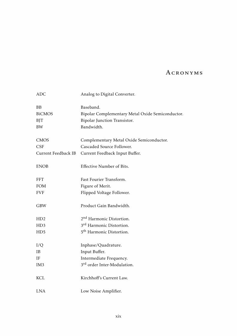
Acronyms
ADC Analog to Digital Converter.
BB Baseband.
BiCMOS Bipolar Complementary Metal Oxide Semiconductor.
BJT Bipolar Junction Transistor.
BW Bandwidth.
CMOS Complementary Metal Oxide Semiconductor.
CSF Cascaded Source Follower.
Current Feedback IB Current Feedback Input Buffer.
ENOB Effective Number of Bits.
FFT Fast Fourier Transform.
FOM Figure of Merit.
FVF Flipped Voltage Follower.
GBW Product Gain Bandwidth.
HD2 2nd Harmonic Distortion.
HD3 3rd Harmonic Distortion.
HD5 5th Harmonic Distortion.
I/Q Inphase/Quadrature.
IB Input Buffer.
IF Intermediate Frequency.
IM3 3rd order Inter-Modulation.
KCL Kirchhoff’s Current Law.
LNA Low Noise Amplifier.
xix

ACRONYMS
MOS Metal Oxide Semiconductor.
MSAAC Matlab tool for Symbolic Analysis of Analog Circuits.
NMOS N-channel Metal Oxide Semiconductor.
OpAmp Operational Amplifier.
OTA Operational Transconductance Amplifier.
PMOS P-channel Metal Oxide Semiconductor.
RF Radio Frequency.
SC Sampling-Capacitor.
SF Source Follower.
SFDR Spurious-Free Dynamic Range.
SNDR Signal to Noise and Distortion Ratio.
SNR Signal to Noise Ratio.
SSF Super Source Follower.
TF Transfer Function.
TH Track-and-Hold.
THD Total Harmonic Distortion.
VCMI Input Common-Mode Voltage.
xx

Chapter
1Introduction
This Chapter provides the motivation and purpose for this project. It points out the main
features of Input Buffers (IBs) and the challenges of its design. Finally, it presents the
organization of this thesis and its main contributions.
1.1 Motivation and Background
Nowadays, most signal processing operations are done in the digital domain, implying
the necessity of having Analog to Digital Converters (ADCs) serving as an A/D interface
between the physical world and the digital world.
For this reason, ADCs have increased the sampling rate, improving the maximum
allowed Bandwidth (BW) of the input signal, converting signals directly from Radio
Frequency (RF). This is a practice to either reduce or eliminate the need for analog mixers
and complex filters. We make these operations in the digital domain with the help of
software.
Presently, the ADC is closer to the antenna on receiver systems. As a result, this kind
of RF ADCs must be able to convert signals with frequencies in the GHz range. Besides
the intrinsic speed necessary of the ADC, these conversions come with another level of
complexity since the Low Noise Amplifier (LNA) might not be able to drive the ADC
without rising significantly the power dissipation of the receiving system.
The driving of the RF ADCs is done by analog buffers, as shown in figure 1.1. This
block drives the ADC without changing the input signal, serving as an interface between
the LNA and the ADC, making those blocks independent of each other. A good buffer
should have the following specifications:
• high linearity, so that it does not alter input signal properties;
• high bandwidth, because the input signal should be at RF range;
1

CHAPTER 1. INTRODUCTION
• low output resistance, so that it can drive the ADC;
• high input impedance, to limit the influence in the input signal;
• low power dissipation targeting handset applications;
• low footprint (area) for reducing cost.
Figure 1.1: High level design of a direct-conversion Receiver System (Rx) comprising anIB and an ADC.
Figure 1.1 represents the direct-conversion front-end architecture. The direct-conversion
is becoming more relevant for its advantages [11]. These advantages include flexibility,
power dissipation, reduced system complexity and reduced weight [7, 10, 11]. The down-
conversion process is done in the digital domain [10] and the Inphase/Quadrature (I/Q)
demodulator can be replace by just one ADC while the demodulation is done in the
digital domain [11].
The LNA on the figure is mandatory for impedance matching of the antenna. As
stated earlier, the input buffer input impedance is desired to be with an high value. This
block connects to the antenna (or the selection filter in the figure) and determines the
performance of the receiver [2]. The LNA is supposed to amplify the input signal with the
minimum noise figure possible [1] while achieving an input impedance matching in all
of the signal bandwidth of 50 Ω [1, 2] to minimize any influence on the receiving signal
[3]. Usually this amplifier is done with a common gate or common source configuration
[23].
An ideal voltage buffer (figure 1.2 a) serves as an interface between two distinct cir-
cuits to eliminate any influence that they can have on one another. Meaning that the
input impedance should be high, and the output impedance should be zero so that the
buffer would be capable of driving whichever load [19], while achieving good linearity
[13]. An Operational Amplifier (OpAmp) in unity gain configuration (figure 1.2 b) can
implement an ideal voltage buffer.
2

1.1. MOTIVATION AND BACKGROUND
(a) Ideal Input Buffer Representa-tion.
(b) OpAmp voltage Input Buffer.
Figure 1.2: High level representation (a) and implementation (b) of a buffer.
Traditionally the most common voltage buffer is the well-known source-follower
(Complementary Metal Oxide Semiconductor (CMOS) transistor in common-drain con-
figuration) shown in figure 1.3, but with some studies, there have been new designs that
implement different buffers with different strengths, that are efficient for some applica-
tions.
Figure 1.3: Basic common-drain topology [12].
Perfect analog unity buffers can be described as circuits characterized by a Transfer
Function (TF) = 1, meaning that the output is a replica of the input. Typically the gain,
defined by the ratio between the output signal and the input signal, is a ratio between 2
expressions. In voltage buffers, usually, there are some similarities between the numerator
and the denominator. If both terms are equal then we have a perfect unity voltage buffer.
3
CHAPTER 1. INTRODUCTION
Let’s imagine that a buffer’s TF is determined by
gm + s ·Cgsgm + s ·
(Cgs +Cgd
) (1.1)
where we see similarities between the numerator and denominator. If the equation (1.1)
is rearranged togm + s ·Cgs[
gm + s ·Cgs]+ s ·Cgd
(1.2)
then the similarities are much easier to perceive. If in equation (1.2) we substitute the nu-
merator by B and the remaining of the denominator by C we can simplify the expression
asB
B+C. (1.3)
emphasizing the problem of analog buffers. Term C is the difference between a real buffer
and an ideal perfect buffer. In a perfect buffer C = 0, which makes equation (1.3) = 1,
for this reason CB is sometimes called follow-up error (FE) meaning the error that takes
the buffer away from the ideal unitary buffer. However, the description of C is valuable
in a real voltage buffer to check how it behaves and how it differs from a perfect buffer
with different frequency ranges.
Since the perfect unity voltage buffer is not achievable, the perfect topology for this
building-block does not exist. Usually, each case uses one architecture that satisfies the
need for each implementation. The main differences rely on optimizing the buffer in some
specifications and compare this new design with others in terms of simplicity, linearity,
and power consumption. There are, however, some topologies that, instead of trying to
achieve a unity gain, ultimately try to achieve higher gains to limit the need for extra gain
blocks in the signal path.
1.2 Objectives and Original Contribution
The first objective of this thesis is to study, simulate, and compare different input voltage
buffer designs already described in the literature. It will examine the ability of these
buffers to work at high speed with a load of 1 pF with a voltage supply of 1.2 V, for 130
nm technology.
The second objective is to propose a new buffer design and do the same tests and
simulations to compare its performance with the state-of-the-art input buffers.
This thesis presents a new functional buffer design described in chapter 5. This archi-
tecture will be explained, with all the considerations taken into account. The proposed
new buffer achieves superior performance when compared with the state-of-the-art. Re-
garding this new architecture, a paper was submitted to ISCAS 2021 with the authorship
of David Leonardo, João Goes and João Melo.
4

1.3. THESIS ORGANIZATION
1.3 Thesis Organization
This work is organized as follows.
In chapter 2 is described as a general idea about voltage buffer designs. It will show
some architectures already published in the literature, deriving their transfer function
and some thoughts about each buffer.
In chapter 3 there will be presented the systematic buffer simulation analysis. It
will show the simulation guidelines that every simulation followed, both in technology,
capacitive load, and sizing of the devices. Furthermore, it explains all the simulations
done and what can be expected to extract from them.
In chapter 4 the simulation results of some of the voltage input buffers, presented in
chapter 2, will be shown. Here, it will be possible to see how each design in previous
works compares to each other when carried out the same analysis.
In chapter 5 a new IB architecture will be presented and studied with the same type
of simulations that every other buffer. The same chapter provides an in-depth analysis of
the new architecture and an improvement to the design.
In chapter 6 will be drawn some conclusions about the work. This final chapter will
reinforce the comparisons between all the buffers, concluding the best performances
between all the designs.
5

Chapter
2review of state-of-the-art
Analog voltage buffers were used for quite some time as output stages of gain blocks, like
Operational Amplifiers (OpAmps) [8, 17, 27], since the gain block first stages’ output
impedance was high and was hard to drive whatever circuitry implemented after the
block. High output impedance would degrade the performance of the circuit comprised
of this block. By implementing a last-stage common-drain class A, B, or AB output buffer,
the output impedance lowers and the block can drive circuits with more ease. Also, this
output stage isolates the gain stages from the load effects.
Nowadays, analog buffers are used for different applications. With the need to down-
convert signals from RF into Baseband (BB) the buffers are used as an isolator from the
effects that come from analog designs like mixers (that could kickback large signals that
could influence the LNA). Eventually, the analog mixer can be removed from the receiving
chain and the ADC can move closer to the antenna. Now, the problem is that the front-
end Track-and-Hold (TH) circuit that samples the input signal to be quantized by the
ADC can be a source of interference and have quite low switched impedance. Therefore,
an input buffer is used as an interface between the input signal and the ADC.
The input buffer needs to isolate the input from the Sampling-Capacitor (SC) sam-
pling stage of the ADC while maintaining to feed the input signal to the ADC with low
distortion. However, this can be difficult to implement as most of the buffers comprise
non-linear devices. The non-linearities of the input buffer severely impact the perfor-
mance of the ADC.
Bearing this in mind, the design of Input Buffer (IB) must follow the specification of
the ADC to minimize the effect of the buffer on the overall ADC dynamic performance.
An input buffer must not just have a high input bandwidth with unity-gain, but also have
high enough Signal to Noise Ratio (SNR), Signal to Noise and Distortion Ratio (SNDR),
Spurious-Free Dynamic Range (SFDR), as well as enough Effective Number of Bits (ENOB)
7

CHAPTER 2. REVIEW OF STATE-OF-THE-ART
to allow driving a moderate to high effective resolution ADC.
This chapter describes several buffer projects in the literature as well as an analysis
of the transfer function of most of these projects. Since some designs are difficult to
analyze by hand, it was used the Matlab tool for Symbolic Analysis of Analog Circuits
(MSAAC) toolbox. MSAAC mainly uses a netlist to derive the transfer function of the
circuit - within a given error.
It is taken into consideration that some of the designs can be used for a multitude of
tasks. As such, they will be shown in the first section as general-purpose designs. Then it
is shown some of the buffers already designed to implement IB for properly driving ADC.
2.1 General Purpose Buffers
Generally, buffers can be used either to interface between circuits or to limit the influence
of a part of the circuit in whatever comes next. For this reason, traditionally, voltage
buffers have been used as the last stage of amplifiers, so that the output resistance of the
amplifier circuit is low and to achieve higher speed. This section shows some possibility
of voltage buffers that can be readily used as input buffers for driving ADCs but due to
their simplicity, they are versatile for other applications.
2.1.1 Common Drain Input Buffer
The classic Source Follower (SF) topology, figure 2.1, can be used as one of the main
building-blocks of current mirrors, differential Operational Transconductance Amplifiers
(OTAs), and class AB output-stage [8], as well as, interfacing with a front-end for ADC.
Due to its simplicity, the common-drain configuration is the first design option for
voltage buffers. The output voltage extracted on the source of a CMOS transistor is
almost a perfect copy of its gate voltage, aside for the Vgs [12]. This fact makes this circuit
a simple yet effective voltage buffer when nominal power-supply is not a big concern (e.g.
VDD > 1.8 V).
A CMOS implementation ensures a minimum input current [6] since the input resis-
tance is defined by the input impedance of the gate of a transistor.
8

2.1. GENERAL PURPOSE BUFFERS
Figure 2.1: Source Follower Design.
Ignoring the body effect and the parasitic capacitances (low-frequency model) and
assuming M2 as an ideal current source, figure 2.2 represents the small-signal equivalent
of figure 2.1. With this, it is possible to extract an approximated TF of the SF.
Figure 2.2: Small-Signal equivalent with Ideal Current Source (no parasitic effects, nobody effect.)
By inspection on figure 2.2, it is possible to obtain an equation that relates vin and vgs,
vgs1 = vin − vout , (2.1)
as well as apply the Kirchhoff’s Current Law (KCL) to the drain node to obtain another
equation that relates vgs and vout
vout ·Rds1 = gm1 ∗ vgs1. (2.2)
By rearranging equation (2.2) and replacing Rds1 for 1gds1
it can be written
vout =gm1
gds1· vgs1, (2.3)
9

CHAPTER 2. REVIEW OF STATE-OF-THE-ART
if (2.1) is substituted in (2.3) then
vout =gm1
gds1· (vin − vout) , (2.4)
where by extracting voutvin
from (2.4) we get the familiar gain expression,
voutvin
=
gm1gds1
gm1gds1
+ 1. (2.5)
If the intrinsic gain gm1gds1
is far larger than 1, then (2.5) could be written as voutvin≈ 1,
which is the ideal buffer. Note, however, that even the SF doesn’t have gain of 0 dB, but it
can be approximately that.
The previous study was done without considering any parasitic effects to simplify the
calculations. However, these should be taken into account since the purpose of this work
is to design high bandwidth buffers. Therefore, it is important to assume the parasitic
effects and find out their impact on the bandwidth. Taking into consideration some of
these effects, the transfer function of the SF can be described as
TF =gm1 + s ·Cgs1
gm1 + gds1 + gds2 + s ·(Cgd2 +Cgs1
) (2.6)
that even without much error (2.6) can still be approximated to a unity gain TF if gm >> gdsand Cgs >> Cgd . However, as frequency increases, the effect of Cgd2 becomes stronger and
it limits the useful bandwidth of the buffer.
This design (Figure 2.1), however, has some limitations that were analyzed and opti-
mized in different studies. Limitations in the output resistance have been studied in [9,
12, 18]. Linearity issues with this design were studied in [21, 25], as well as studies to try
and overcome the offset at the output [9].
One of the major problems with this topology is the non-linearity that comes with a
lack of isolation of just a single transistor [21] and the strong dependence of vgs regarding
signal variations.
On another note, even though this configuration theoretically has the lowest output
resistance of all the three single transistor configurations, the output resistance (Ro) is
roughly around 1/gm, in [12, 22] the output resistance is calculated to be
Rout =1
gm + gmb||RL, (2.7)
where Rout is the output resistance, gm is the intrinsic gain of the device, RL is the load of
the buffer and gmb represents the body-effect transconductance. This value can be around
some kΩ and thus may be higher than expected. This makes it necessary to increase the
bias current and increase the aspect ratio WL , increasing the power dissipation and the
area of the buffer [16].
10

2.1. GENERAL PURPOSE BUFFERS
2.1.2 Cascaded Source Follower Input Buffer
One of the issues associated with the simple source follower is the DC level shifting. This
can be more or less problematic depending on each specific problem and application.
In [26] is presented a design with offset cancellation on the output. This design uses
two cascaded complementary source followers to reduce the offset at the output. As
shown in figure 2.3 the Cascaded Source Follower (CSF) uses two level-shifters to cancel
the offset effect that appears when using just one of them.
Figure 2.3: Cascaded Source Follower Design.
This can, ultimately, reduce the offset of vo − vi to vgs2 − vgs1 that can be theoretically
zero but a simple change on the process or working temperature can alter the offset [26].
As far as the transfer function, assuming that M3 and M4 are ideal current sources,
the TF can be approximated to
TF =gm1 · gm2 + s ·
(Cgs1 · gm2 +Cgs2 · gm1
)gm1 · gm2 + gm1 · gds2 + gm2 · gds1 + s ·
(Cgd2 · gm2 +Cgs1 · gm2 +Cgs2 · gm1
) . (2.8)
Taking a look at equation (2.8) it is possible to describe it as a buffer by rearranging
some of the terms
TF =gm1 · gm2 + s ·
(Cgs1 · gm2 +Cgs2 · gm1
)[gm1 · gm2 + s ·
(Cgs1 · gm2 +Cgs2 · gm1
)]+ gm1 · gds2 + gm2 · gds1 + s ·
(Cgd2 · gm2
) . (2.9)
However, this TF was simplified by considering M3 and M4 as ideal current sources.
If that was not the case, the corruption factor on (2.9) would be larger thanks to the
parasitic capacitors on both of these transistors.
This architecture has some improvements in maintaining the Input Common-Mode
Voltage (VCMI) at the output but it does still have the same problem with the output
resistance of the basic Source Follower, meaning that power dissipation can be an issue.
11
CHAPTER 2. REVIEW OF STATE-OF-THE-ART
2.1.3 Super Source Follower Input Buffer
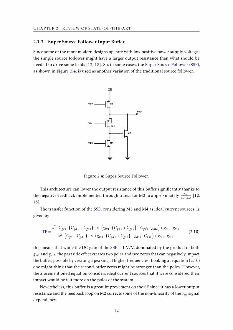
Since some of the more modern designs operate with low positive power supply voltages
the simple source follower might have a larger output resistance than what should be
needed to drive some loads [12, 18]. So, in some cases, the Super Source Follower (SSF),
as shown in Figure 2.4, is used as another variation of the traditional source follower.
Figure 2.4: Super Source Follower.
This architecture can lower the output resistance of this buffer significantly thanks to
the negative-feedback implemented through transistor M2 to approximately gds1gm1·gm2
[12,
18].
The transfer function of the SSF, considering M3 and M4 as ideal current sources, is
given by
TF =s2 ·Cgs1 ·
(Cgd1 +Cgs2
)+ s ·
(gm1 ·
(Cgd1 +Cgs2
)−Cgd1 · gm2
)+ gm1 · gm2
s2 ·(Cgs1 ·Cgd1
)+ s ·
(gm1 ·
(Cgd1 +Cgs2
)+ gds1 ·Cgs1
)+ gm1 · gm2
(2.10)
this means that while the DC gain of the SSF is 1 V/V, dominated by the product of both
gm1 and gm2, the parasitic effect creates two poles and two zeros that can negatively impact
the buffer, possible by creating a peaking at higher frequencies. Looking at equation (2.10)
one might think that the second-order zeros might be stronger than the poles. However,
the aforementioned equation considers ideal current sources that if were considered their
impact would be felt more on the poles of the system.
Nevertheless, this buffer is a great improvement on the SF since it has a lower output
resistance and the feedback loop on M2 corrects some of the non-linearity of the vgs signal
dependency.
12
2.2. INPUT BUFFERS DESIGN
2.1.4 Flipped Voltage Follower Input Buffer
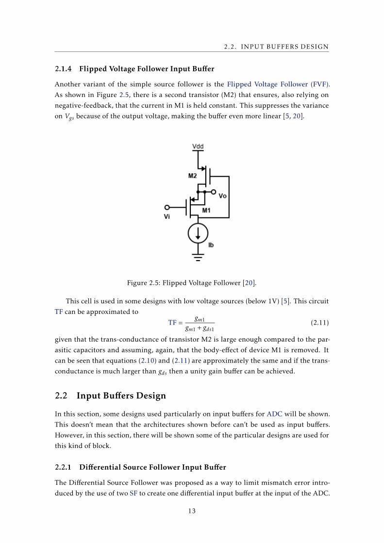
Another variant of the simple source follower is the Flipped Voltage Follower (FVF).
As shown in Figure 2.5, there is a second transistor (M2) that ensures, also relying on
negative-feedback, that the current in M1 is held constant. This suppresses the variance
on Vgs because of the output voltage, making the buffer even more linear [5, 20].
Figure 2.5: Flipped Voltage Follower [20].
This cell is used in some designs with low voltage sources (below 1V) [5]. This circuit
TF can be approximated to
TF =gm1
gm1 + gds1(2.11)
given that the trans-conductance of transistor M2 is large enough compared to the par-
asitic capacitors and assuming, again, that the body-effect of device M1 is removed. It
can be seen that equations (2.10) and (2.11) are approximately the same and if the trans-
conductance is much larger than gds then a unity gain buffer can be achieved.
2.2 Input Buffers Design
In this section, some designs used particularly on input buffers for ADC will be shown.
This doesn’t mean that the architectures shown before can’t be used as input buffers.
However, in this section, there will be shown some of the particular designs are used for
this kind of block.
2.2.1 Differential Source Follower Input Buffer
The Differential Source Follower was proposed as a way to limit mismatch error intro-
duced by the use of two SF to create one differential input buffer at the input of the ADC.
13

CHAPTER 2. REVIEW OF STATE-OF-THE-ART
This approach originally proposed in [16], instead of using two completely independent
SF for each one of the differential inputs, introduces a differential loop between the two
SF [16].
Using a fully-differential topology improves the performance of the design by ideally
cancelling the even-order harmonics. Otherwise, merely duplicating most parts of the
circuit may lead to area and power dissipation increase [4].
In figure 2.6 it is shown the design of the differential source follower input buffer.
Figure 2.6: Differential Source Follower IB [16].
Using a cross-coupled pair at the output nodes with transistor M3 and its counterpart
the even-harmonic distortion is further attenuated. However, this affects the performance
of the circuit in terms of bandwidth and gain [16].
2.2.2 Differential Super Source Follower Input Buffer
The Super Source Follower was proposed to decrease output resistance and thus increase
the bandwidth of the buffer, making it able to work at higher frequencies [16]. However,
this approach was single-ended and, consequently, two independent circuits are used
when buffering a fully-differential input. This can bring mismatch errors between the
two circuits and, ultimately, it can degrade the linearity. In figure 2.7 it is represented by
a differential super source follower design.
14

2.2. INPUT BUFFERS DESIGN
Figure 2.7: Differential Super Source Follower IB [16].
Similarly to the Differential Source Follower, the Differential Super Source Follower
creates a cross-coupled loop between the two circuits, to make a fully differential circuit.
In [16] it is reported that this technique improves buffer linearity and speed, while also
having the added benefit of having active gain in the buffer.
2.2.3 Input Buffer with Current Feedback
The Current Feedback Input Buffer (Current Feedback IB) differs from the SSF since its
feedback is done by current instead of voltage. This feedback maximizes the linearity of
the simple Source follower architecture [24].
Figure 2.8 shows one design with current feedback. In it, the main device M1’s drain
voltage is used to regulate the Vgs of M2. This will regulate the current flowing on M2’s
branch that is mirrored by a wide-swing dynamic cascode current mirror composed by
M3 and M4. This feedback is controlled by the current mirroring factor between devices
M3A and M3B, and devices M4A and M4B.
Analyzing the feedback loop on figure 2.8 it is possible to conclude that there is some
positive feedback. If the voltage Vin increases then increases the voltage Vgs on transistor
M1 which makes the current flowing through the transistor larger. This in turn increases
the voltage on the source Vout and lowers the one on the drain. By lowering the voltage
at the drain of M1, the same voltage applied to the source of M2, this lowers the current
flowing in M2 because the Vgs of this transistor decreases. By decreasing the current the
voltage on the drain of M2 decreases which decreases the Vgs of M3A, making the current
15

CHAPTER 2. REVIEW OF STATE-OF-THE-ART
Figure 2.8: Current Feedback Input Buffer.
flowing on the cascode smaller and, consequently, increasing vout.
Parasitic capacitance in the feedback loop needs to be minimized so that the AC cur-
rent lost to charge these parasitic capacitors is kept at a minimum [24] and the feedback
is fast enough to improve the signal bandwidth.
This input buffer transfer function is given by
TF =2 · gm2 · (gm4 + 2 · gds4)
2 · gm2 · (gm4 + 2 · gds4) + s ·Cgd5 · gm4(2.12)
this makes this circuit fairly dependent on frequency. Taking into consideration (2.12)
this circuit acts as an ideal buffer until the effect of the parasitic capacitor Cgd5 is felt.
2.2.4 Push-Pull Input Buffer
Another way of designing an input buffer is by using a push-pull configuration design
[14].
As shown in figure 2.9 this buffer is an AC-coupled class-AB push-pull source follower.
The decoupling of the input means that this block cannot be used as a low-frequency
buffer. However, it does not need another low-pass filter for applications at higher fre-
quencies, where a baseband might not be needed.
As stated before, this design has an AC coupling at the input to each gate of the
devices. The bias point is achieved by generating each voltage from VB1 to VB4. The
resistors need to be sized to not change the input value at each device. Since all the
devices above Vin and Vout are N-channel Metal Oxide Semiconductor (NMOS) and all
devices below are P-channel Metal Oxide Semiconductor (PMOS) then when the input
rises the NMOS devices pull the output since the Vgs of said devices will increase, while
the PMOS devices push it because their Vgs will decrease. If the input lowers then the
16

2.2. INPUT BUFFERS DESIGN
Figure 2.9: Push-Pull Input Buffer [14].
reverse happens. Because of this behavior, this configuration is called a "push-pull"input
buffer.
Another drawback of this circuit is due to the requirement of a positive (high) supply
voltage (VDD) together with a negative VSS. In [14], VDD = 1.35 V and VSS = -0.45 V have
been used.
Push-pull source followers are commonly used as the last stages of amplifiers for their
power dissipation optimization and providing the required low output resistance.
2.2.5 Vgs-controlled Cascaded Source Follower Input Buffer
The CSF tries to guarantee that the output common mode be equal to the input common
mode. As stated before there are some mismatch problems with just using two cascaded
source followers. There are a number of techniques that can improve the performance of
th CSF [26]. One of these uses a negative feedback loop to control the Vgs of the cascaded
common-drain device. Figure 2.10 shows the technique design.
17

CHAPTER 2. REVIEW OF STATE-OF-THE-ART
Figure 2.10: Cascaded Source Follower with Vgs control [26].
The negative feedback reduces output impedance and keeps Vgs2 ≈ Vgs1, reducing
both constant and input-dependent component of the output signal. M3’s gate and source
are connected to M1’s source and gate, respectively, to sense any variation on Vgs2. M1
and M3 form a differential-pair with a current-mirror load comprised of M4 and M5.
If there is any variance in Vgs of the common-drain devices, the gate voltage of M9 is
adjusted to change the current trough M2 until Vgs1 ≈ Vgs2.
2.3 Other implementations
Some other types of implementation were not covered in this chapter but can be consid-
ered.
2.3.1 BiCMOS solution
This solution (Figure 2.11), described in [6], uses BiCMOS technology to improve linearity
while attempting to maintain a high speed. This solution was not considered since it uses
BiCMOS technology while this work only focuses on CMOS technology.
This buffer comprises a two-stage OpAmp in a unity gain configuration, using a
global feedback solution [6]. The first stage is a PMOS differential pair with some Bipolar
Junction Transistor (BJT) as an active load. In the last stage, there are two more BJT in
a Darlington structure. To keep the output with the same value as the input, the first is
18

2.4. FINAL THOUGHTS
Figure 2.11: BiCMOS PMOS input buffer [6].
feedback to the M1 device that is the counterpart of the differential pair of the input. If
the input changes, the current from 2I becomes unbalanced in the differential pair and
the circuit will converge to the point where the output equals the input.
2.4 Final thoughts
Every implementation of input buffers shown and described in this chapter was trying to
answer some particular problems of previous designs. In the following chapters of this
work, some of these architectures will be simulated on the same basis to achieve some
understanding of the best architectures for this work.
In the next chapter, it will be shown an overview of the simulation guidelines that are
followed in this work. As well as want will be the priorities to achieve and what are the
constraints that were imposed. It will be also shown, an overview of the simulation setup
used in every simulated buffer and how every device on the design was sized.
19


Chapter
3Study and simulation of the voltage buffers
3.1 The Process Guidelines and Simulating Conditions
In this chapter, it will be discussed the sizing and the simulation of some of the buffers
shown in Chapter 2 (review of state-of-the-art) as well as comparisons between them.
With that in mind, this work was done with some specifications (Table 3.1), so that
the comparisons can be done with fairness. This means that these specifications have
been used to systematize the process for all the designs to be simulated in a comparable
condition.
Table 3.1: Specifications of the simulation.
Technology 1.2 V, 130 nm CMOSCapacitive Load 1 pFInput impedance > 10 MΩ
Open Loop Gain ≈ 1 V/VDevices type No IO devices; Only standard core devices are used
Voltage Supply 1.2 V ± 10%
Besides the contents on Table 3.1, there was the need to size all the transistors similarly.
Otherwise, some misconceptions could be made regarding the operation of the circuits.
For this reason, the transistors were divided into three different groups so that their sizing
could follow a systematic design procedure.
Current Biasing - The transistors that implemented the ideal current source to bias the
buffer;
Main Buffer Transistors - The main transistors that implemented the common-drain
buffering function;
21

CHAPTER 3. STUDY AND SIMULATION OF THE VOLTAGE BUFFERS
Feedback - The implemented current mirror to create either negative or positive feed-
back.
All the transistors in every different design but within the same group were sized
in the same way, with NMOS transistors having a different sizing than the PMOS. The
voltage setup was made by a similar circuit in every design, with some room to optimize
said voltages, mainly so that all the transistors were in the saturation regime (i.e. the
active region).
3.2 Sizing
This section will describe the sizing of each group talked about in Section 3.1. For this,
the simplest design, the Source Follower (Section 2.1.1), will be used as a reference circuit
and the process to size will be shown.
Figure 3.1 shows the design of the source follower. In this design, M1 is the buffer
transistor NMOS while M2 acts as a current source.
Figure 3.1: Source Follower.
This means that M1 will be sized as in the "Main Buffer"transistor group and M2 as
in the "Current Biasing"group.
3.2.1 Sizing Main Buffer Transistors
Starting with M1, "Main Buffer"Transistors will be designed with speed as a major concern,
this means that the channel length used will be set to the minimum possible. In the given
technology it is 120 nm. The Vdsat will be chosen at around 100 mV ±25 mV so that the
signal can have a dynamic range high enough for future designs. Lastly, the current used
in buffer transistors is 1 mA as shown in Table 3.1.
With these values, knowing that the drain current, for the strong inversion region, of
the transistor (ID ) can be approximated to
ID =K2· WL·(Vgs −Vth
)2(3.1)
22

3.2. SIZING
where Vgs is the voltage from the gate to the source of the transistor and Vth is the thresh-
old voltage needed for the transistor to start conducting and assuming that the transistor
is in strong inversion Vgs −Vth ≈ Vdsat then, if this is done to equation (3.1)
ID =K2· WL·V 2
dsat (3.2)
where ID is the biasing current of the transistor, K is a technological design parameter,
W is the channel width and L is the channel length. Since the only value not know is the
channel width it’s possible to solve equation (3.2) regarding that parameter as
W =2 · ID ·LK ·V 2
dsat
. (3.3)
The channel length (L) used for these transistors was the technology minimum channel
length. Using the minimum value for L increases the speed of the transistor and, because
of this, increases the bandwidth of the buffer. Since we want high speed input buffers it is
recommended to use lower channel length. Solving equation (3.3) the designated values
can be seen as
W =2 · 1000 · 120 · 10−9
500 · 0.12 (m) (3.4)
which means that the channel width of NMOS buffer transistors should be W = 48 µm.
In Table 3.2 is shown the dimensions of NMOS and PMOS Buffer Transistors.
Table 3.2: Buffer Transistors Sizing.
Buffer Transistors
NMOS PMOSL W L W
120 nm 48 µm 120 nm 160 µm
Some important actions were taken regarding the body-effect of these devices. Bear-
ing in mind that the body-effect trans-conductance limits the gain of the block. This
attenuation is particularly important in buffer designs since the buffer does not achieve
high gains the body-effect will most assuredly create an attenuation. This attenuation can
be less noticeable if the body effect is taken out of the main buffer devices. This means
that every bulk of any transistor in a common-drain configuration has been shorted to
the source of the same device, so that the voltage between source and bulk is zero and
there is no body-effect, this is valid for every advanced "triple-well"process.
3.2.2 Sizing Current Biasing Circuitry
Current Biasing transistors define the current that flows in each branch of the circuit. The
way it was implemented in this work is simply from the use of multiplier transistors. This
means that the voltage bias circuit was implemented with certain sized transistors and the
current biasing transistors are equal in size and replicated the number of times necessary
23
CHAPTER 3. STUDY AND SIMULATION OF THE VOLTAGE BUFFERS
to provide a multiplied current. If, for example, we had a voltage biasing transistor MBIAS
that creates a voltage VBIAS with a current IBIAS, if in the branch that its implemented a
current source with 10 × IBIAS, then that means that the implementation of that source
would be ten parallel transistors equal to MBIAS.
In Table 3.3 there are discriminated all of the base transistors and their driving current
for each of the BIAS voltages.
Table 3.3: Current Sources Sizing.
PMOS NMOS
VBP VCASP VCASN VBNL W L W L W L W
360 nm 48 µm 360 nm 5.3 µm 480 nm 2.7 µm 360 nm 14.4 µm
3.2.3 Sizing Feedback
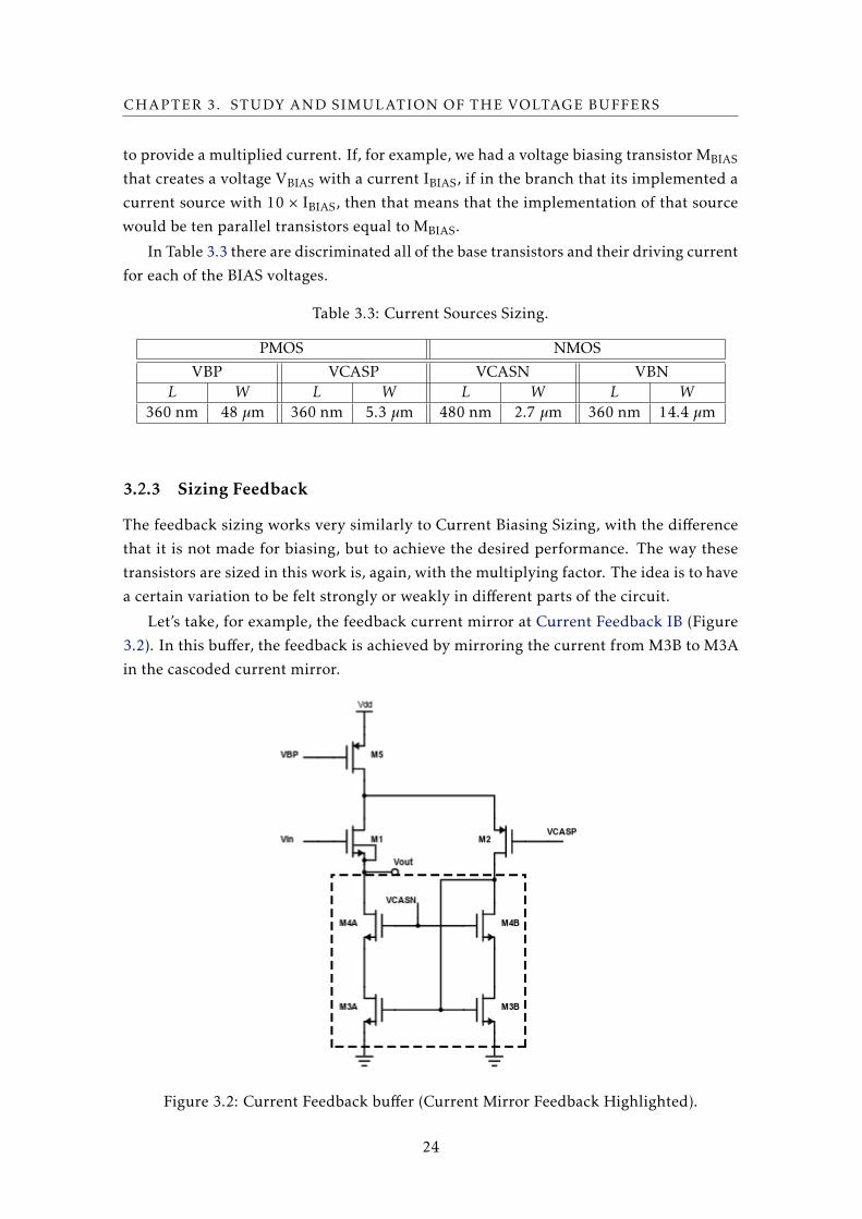
The feedback sizing works very similarly to Current Biasing Sizing, with the difference
that it is not made for biasing, but to achieve the desired performance. The way these
transistors are sized in this work is, again, with the multiplying factor. The idea is to have
a certain variation to be felt strongly or weakly in different parts of the circuit.
Let’s take, for example, the feedback current mirror at Current Feedback IB (Figure
3.2). In this buffer, the feedback is achieved by mirroring the current from M3B to M3A
in the cascoded current mirror.
Figure 3.2: Current Feedback buffer (Current Mirror Feedback Highlighted).
24

3.3. SIMULATION TESTBENCH
If the feedback mirroring factor needs to be 1:4 [24], then this means that M3A needs
to be made of 4 transistors the same size as M3B so that the size of the later is 4 times
smaller than the first.
3.3 Simulation testbench
For all simulations, the same setup was used. This setup was a high-level design with
all the simulated outside influence as shown in figure 3.3. It is shown that there is no
input interference to the buffer, as well as no AC coupling. This was used so that the DC
of the signal was the one injected at the input of the buffer and was easier to achieve the
pretended value, given by the voltage source.
Figure 3.3: Simulation testbench for all the simulated buffers.
It is possible to check that the output is modeled as a single load capacitor with a
normalized value of 1 pF. This model some of the effects of the circuit that follows the
buffer. The value of the capacitor was the same between simulations. Because of this,
bandwidth values were achieved in the same conditions between all simulations.
All of the buffers have been simulated in a differential simulation to increase the
dynamic range of the output signal and some better noise and distortion values. The
circuits are the same circuit replicated with differential input voltages. This simulation
setup was used in all non-differential designs to achieve a pseudo-differential buffer.
Talking more about the DC operating point, the voltages were mainly achieved by
a single circuit common to all simulated buffers. However, even though the schematic
of the current mirrors was always the same, the sizing of the devices was not. This
was necessary to achieve some variance between DC operating points between all of the
designs. In figure 3.4 it is shown this same schematic and the only devices tuned in each
25

CHAPTER 3. STUDY AND SIMULATION OF THE VOLTAGE BUFFERS
buffer simulation were M1 and M8, the ones achieving the cascode biasing voltages VCASP
and VCASN, respectively.
Figure 3.4: Current Mirror used to BIAS all the simulated circuits.
From the DC supply to the input supply, the input signal had three components that
were simulated. The first one was the common-mode component of the signal. The
common-mode was used to bias the circuit into the preferred operating point. This value
was tuned with DC simulation until all the devices were in the desired region for their
operation. The second input signal component simulated was the AC component. This
one was used to simulate the buffer with varying frequency of the input signal to obtain
the bode diagram and the bandwidth. Lastly, a sinusoidal wave was supplied to the input
of the buffer to be used in a transient simulation. This wave’s properties were adjusted to
have an output signal wave with around 600 mV (≈ VDD/2) amplitude and the frequency,
although shared between all buffers, was chosen with the results of the AC simulations.
Even though all the simulation had the same simulation testbench, the input signal’s
components varied depending on the buffer. The only factor that was constant across
every design was the frequency of the input signal. Both the common-mode and the input
amplitude were changed depending on the desired performance of the buffer.
3.4 Simulations setup and objectives
In this section, some of the objectives behind every simulation will be presented. This
section will not look at any result of any buffer, instead, it will indicate what were the
ideas and thought process behind every simulation, as well as mentioning every few
aspects worth noting in the next chapter.
26

3.4. SIMULATIONS SETUP AND OBJECTIVES
3.4.1 DC Simulation
The main objective of the DC simulation was to verify and tune the operation point of
every transistor. DC values of current and Vgs voltages were checked if they were within
parameters or if there were any possible improvements.
The output common-mode was checked to see if the buffer would work with all the
restrictions. This value would have to be enough to keep all of the transistors in saturation
(i.e. active region) even with the variation of the signal.
Another important point was the output driving current, for comparison purposes.
While the total DC current was necessary to compare the power dissipation between
buffers, the output current should be around the same values regardless of the architec-
ture so that the comparison between bandwidths of the designs is kept in the same fair
conditions in every buffer.
3.4.2 AC Simulation
The AC simulation served two purposes. The first one being the bandwidth value of
every simulated buffer and the second one being the choice of the input frequency for the
transient analysis.
Regarding bandwidth, all of the buffers were simulated with a varying frequency from
1 Hz to 100 GHz and all bode’s gain and phase diagrams were plotted. From these graphs,
a few things were accounted for later comparisons. The DC gain, or lack thereof, to
compare the need for higher amplitudes at the input. As a reminder, the transient-noise
simulation was done to keep an output amplitude of 600 mV. Maintaining this value with
a strong attenuation could be impractical at the input. Another important characteristic
was the flatness of the band. Some designs have frequency peakings that can severely
impact the expected performance of the buffers at higher frequencies.
Ultimately, the results of these simulations were used to get a value of frequency high
enough to keep the circuits at some stress levels. The frequency chosen would need to
be the same in all of the buffers. That meant that the stress level would not be equal in
all designs. However, it was decided that keeping the same frequencies would suit better
and fairer comparisons.
3.4.3 Transient-noise Simulation
The last analysis was transient-noise analysis. All the circuits were simulated with 100
cycles of the input with a constant frequency. These simulations were done following the
results of the prior simulations.
The transient-noise simulation was used to simulate every circuit reaction to a "real"signal.
This simulation was stressed to an input signal with a certain amplitude, to achieve the
targeted output amplitude and frequency consistent between buffers.
27

CHAPTER 3. STUDY AND SIMULATION OF THE VOLTAGE BUFFERS
This simulation has been used to calculate the Fast Fourier Transform (FFT) of the
output signal. With the FFT calculated some values were extracted from it. Namely
the SNDR and the Total Harmonic Distortion (THD) between others. Even though the
distortion is usually compared regarding THD, the values of distortion of the first five
harmonics were calculated independently, named 2nd Harmonic Distortion (HD2) to 5th
Harmonic Distortion (HD5). As stated in the last section (AC Simulation), the amplitude
of the output in these simulations was set to be about 600 mV (≈ VDD/2). This was done
so that the comparisons between buffers were, once again, done with similar conditions
among buffers.
Another aspect of this analysis is that it was prepared to allow the double-tone simula-
tion, by having two different input signals with similar frequency and the same amplitude.
This simulation gives a metric of how the circuit reacts to a signal composed of two differ-
ent frequencies close to each other. The maximum differential output swing was, again,
set to 600 mV.
One important note to make when talking about FFT is to have some coherent window
to minimize spectral leakage. In this work, the coherent window was achieved by making
the input frequency a multiple of a frequency bin. This frequency bin is a function of
the sampling frequency, in this work 2 GHz, and the number of points per period. These
bins were also used for the inter-modulation analyzes, by having both frequencies one
bin shift from the frequency chosen for the input signal on a regular transient simulation.
The next chapter describes the simulation study of some voltage-buffer architectures
presented in chapter 2 - review of state-of-the-art - following the details of this chapter.
In the end, the information is summarized in a table regarding the most important values
of the simulations.
28

Chapter
4Analysis and Results of the state-of-the-art
Continuing from the last chapter, this one presents the results of the electrical simulations.
These reports discriminate each simulation in each design. Comparisons between the sim-
ulations’ results are made. Finally, the designs will be categorized for their performance,
advantages, and disadvantages.
Every simulated buffer was analyzed independently with the same procedure. Firstly,
each architecture shows some results regarding the DC simulation. With this, we validate
the DC bias operating point of each device and annotate currents values.
Secondly, we use the AC analysis to compare each bandwidth and acknowledge the
input frequency for the transient-noise analysis, as stated in Chapter 3 - Study and simu-
lation of the voltage buffers.
Finally, a more extensive transient-noise analysis is done. This simulation allows us
to compare the different values of distortion and noise that affect each design.
4.1 Source Follower Input Buffer Analysis
This section will present the three analyses of the basic Source Follower (SF). Being the
simplest circuit, there were no problems to size and simulate it.
4.1.1 DC Analysis (SF)
The sizing of the circuit was easy to achieve, as only two devices comprise this buffer,
one of which is a current source to the buffer main-device. The main concern was to
get the current to be as close as possible to the nominal 1 mA target. Figure 4.1 shows
the current to be approximately the target current. The same figure shows room for the
output to achieve 150 mV amplitude, pretended for the transient-noise analysis 600 mV
peak-to-peak differential amplitude.
29

CHAPTER 4. ANALYSIS AND RESULTS OF THE STATE-OF-THE-ART
Figure 4.1: Source Follower DC Operating point.
Note that the bias voltage VBN was achieved with a current mirror not shown in the
schematic. The circuit used to achieve said voltage was shown in figure 3.4 on page 26.
The sizing for this circuit was chosen to have the VBN necessary for the desired operating
point of the circuit.
4.1.2 AC Analysis (SF)
The AC analysis of the SF had not many problems. With only one pole at the output, the
design is always stable. Figure 4.2 shows that the gain of the block is close to 1 V/V (0
dB). The system is dominated by one pole that influences the frequency response since
the gain is constant until a frequency when it decays about 20 dB per decade.
Figure 4.2: Source Follower Frequency Response.
Lastly, it is important to point out that the simulated bandwidth of the system is
around 1.5 GHz. This is the point when the gain degrades 3 dB compared to the initial
value.
30

4.1. SOURCE FOLLOWER INPUT BUFFER ANALYSIS
4.1.3 Transient-noise Analysis (SF)
The transient-noise analysis for the SF was easy to tune for the target output amplitude
voltage as shown in figure 4.3. This figure shows just the output signal and it looks
like a perfect sinusoidal wave. However, to be able to measure the distortion value it is
necessary to get the FFT of this signal.
Figure 4.3: Source Follower Output (time).
The signal FFT is shown in figure 4.4. With this figure, we can see some trends. First,
the DC power bin/spur (i.e. the offset bin) is minimal (around -100 dB) this happens
because the output is differential, meaning that the common-mode at each branch cancels
one another. Second, the strongest power spur comes from the frequency of the input
signal meaning that the wave that we saw in figure 4.3 is close to the input frequency.
There are another two points marked in figure 4.4, the second is with double the frequency
of the input signal and the third with three times the frequency of the same signal. These
points are harmonics of the signal, used to calculate HD2 and 3rd Harmonic Distortion
(HD3) respectively, and the lower they are the lesser the harmonic distortion of the output
signal.
Figure 4.4: Source Follower Output (frequency).
Paying attention now to the inter-modulation analysis, figure 4.5 shows the mix of
two different frequency signals.
The signal FFT is shown in figure 4.6. Here it is possible to see two different peaks;
these are the fundamental harmonics of the two tones selected for this analysis. The two
31

CHAPTER 4. ANALYSIS AND RESULTS OF THE STATE-OF-THE-ART
Figure 4.5: Source Follower 2 Tone Analysis Output (time).
other marked points are the points to calculate the 3rd order Inter-Modulation (IM3). This
value is the difference between the lowest fundamental harmonic power (in this case 125
MHz) and the highest power of the inter-modulation (in this case 62.5 MHz).
Figure 4.6: Source Follower 2 Tone Analysis Output (frequency).
All the results are compiled in table 4.1. These include results from all 4 different
analyses.
Table 4.1: Summary from the Source Follower Simulation Analysis.
Current 2 mABandwidth 1.5 GHz
DC Gain -0.7 dBInput Frequency 109 MHz
Offset Spur -121 dBHD2 -80 dBHD3 -55 dBIM3 70 dB
SFDR 55 dBENOB 8.0 bits
Current refers to the sum of all of the currents flowing through the differential circuit.
In figure 4.1 the operation point shown is just one of the circuits meaning that the current
32

4.2. SUPER SOURCE FOLLOWER INPUT BUFFER ANALYSIS
is doubled when a differential circuit is used. These values will be used as a reference for
all future results.
4.2 Super Source Follower Input Buffer Analysis
This section will present the three analyses of the Super Source Follower. This circuit was
meant to be an improvement over the last one. With the voltage feedback, the output
resistance decreases and the bandwidth should increase.
4.2.1 DC Analysis (SSF)
The sizing of the circuit followed the following guidelines. The current through PM1, the
main device, was set to be 1 mA. Meanwhile, the feedback current, through NM1, was
set to be around 14 of the value through the main device. The DC operation bias point of
the circuit is visible in figure 4.7.
Figure 4.7: Super Source Follower DC Operating point.
4.2.2 AC Analysis (SSF)
The AC analysis of the SSF, figure 4.8, showed the first problems with complex buffer
systems. With 2 poles and 1 zero, the frequency response of this buffer shows a peaking
close to the cutoff frequency. This peaking can degrade some of the linearity performance
of the buffer at a higher frequency.
It is also important to note that the registered bandwidth is 1.7 GHz. Even though
increasing the current through the feedback device would improve the bandwidth, by
doing it, the peaking shown would increase as well.
33

CHAPTER 4. ANALYSIS AND RESULTS OF THE STATE-OF-THE-ART
Figure 4.8: Super Source Follower Frequency Response.
4.2.3 Transient-noise Analysis (SSF)
In this simulation, the target output voltage of 600 mV was achieved without problems
(Figure 4.9), and the results were as expected. Again, the sinusoidal wave is not able to
give information about the linearity performance of the buffer, for that, it is necessary to
transform the time signal to the frequency domain.
Figure 4.9: Super Source Follower Output (time).
The signal FFT is shown in figure 4.10. Like what was shown in the SF section, the
DC value is negligible and the input frequency is the strongest signal shown. In this case,
the HD2 is far more attenuated compared to other frequencies, while HD3 is still the
strongest harmonic of the signal.
Regarding the two-tone analysis, the same pattern can be seen in time in figure 4.11.
Again looking at the time wave gives little to no information.
Looking at the signal FFT, however, can show a lot more information. Again it is
possible to see the two-tone frequency in addition to the power of the IM3.
Table 4.2 shows some of the numeric results of these simulations showing the perfor-
mance of the simulated circuit.
34

4.2. SUPER SOURCE FOLLOWER INPUT BUFFER ANALYSIS
Figure 4.10: Super Source Follower Output (frequency).
Figure 4.11: Super Source 2 Tone Analysis Follower Output (time).
Figure 4.12: Super Source Follower 2 Tone Analysis Output (frequency).
Table 4.2: Summary from the Super Source Follower Simulation Analysis.
Current 2.6 mABandwidth 1.7 GHz
DC Gain -0.8 dBInput Frequency 109 MHz
Offset Spur -105 dBHD2 -85 dBHD3 -61 dBIM3 66 dB
SFDR 61 dBENOB 8.5 bits
35

CHAPTER 4. ANALYSIS AND RESULTS OF THE STATE-OF-THE-ART
Comparing the results from table 4.2 and 4.1 on page 32, it is possible to understand
that the SSF has some advantages compared to the SF. There is a 6 dB increase in harmonic
distortion and the ENOB rises half a bit. However, the bandwidth decreases contrary to
what was expected. As stated before the bandwidth of the SSF can increase but that
will increase the frequency peaking, visible in figure 4.8. This decrease in bandwidth
happened because the SSF was not sized to the best performance. Note that the current
flowing through the main device need to be the same to derive some conclusions and that
current can be, in some way, not ideal for this design, when compared to the SF.
4.3 Cascaded Source Follower Input Buffer Analysis
The Cascaded Source Follower is an improvement from a single-ended Source Follower.
The main concept of this buffer is to eliminate the common-mode shift between output
and input. Even though this problem is not as present in the differential signal domain,
the same analysis was made to this buffer.
4.3.1 DC Analysis (CSF)
Since the CSF is in its essence two SF. The sizing of the circuit was made by having two
1 mA branches. However, this can be optimized since the first branch drives the second.
Since the second branch load should be around the fF range, it is possible to reduce the
first stage current to limit the overall circuit’s power dissipation. However, the currents
were sized to 1 mA in both stages, as shown in Figure 4.13.
Figure 4.13: Cascaded Source Follower DC Operating point.
As stated before, this buffer meant to keep the common-mode from the input at the
output. To achieve this both Vgs of the two main devices (PM0 and NM0) should be the
36

4.3. CASCADED SOURCE FOLLOWER INPUT BUFFER ANALYSIS
same. Since this circuit would be used in a differential topology this problem was not
addressed on its sizing. However, with close inspection of the values of Vgs it is possible
to see that, without the differential pair, the output common-mode would be shifted by
50mV compared to the input common-mode.
4.3.2 AC Analysis (CSF)
Since the output stage of this buffer is a regular Source Follower it was not expected to
have any improvement in the bandwidth of this system and because of the absence of
zeros from the system, it was not expected to have any peaking in the frequency. This
assumption can be confirmed by figure 4.14 where the frequency response of the CSF is
shown.
Figure 4.14: Cascaded Source Follower Frequency Response.
Lastly, it is important to point out that the bandwidth of the system is around 1.6
GHz.
4.3.3 Transient-noise Analysis (CSF)
The transient-noise analysis for the CSF was as simple to set up as the SF one. The
cascaded nature does have a small impact on the attenuation of the signal however that
was not a major problem for this circuit. Figure 4.15 shows the signal variance across
time. The voltage achieved is around 600 mV peak to peak with a differential output.
The time-domain of the signal does not show the distortion caused by the circuit,
for that it was used a FFT to transform the time domain to frequency domain shown in
figure 4.16. Here it is possible to see the same peak at the input frequency and all of the
output signal’s harmonics. Note that, even though the CSF was supposed to decrease the
common-mode of the system, the DC power in figure 4.16 is around 100 dB like every
other circuit shown previously. This happens since the common-mode cancellation is
done with a differential topology, meaning that the single-ended topology does not need
any common-mode cancellation.
To check the inter-modulation distortion, a two-tone signal was used at the input. In
figure 4.17 the output of the buffer is shown. In close inspection, it is possible to see
37

CHAPTER 4. ANALYSIS AND RESULTS OF THE STATE-OF-THE-ART
Figure 4.15: Cascaded Source Follower Output (time).
Figure 4.16: Cascaded Source Follower Output (frequency).
that the signal is somewhat different from the signal at figure 4.11 on page 35, yet this
difference is expected and shown in the FFT of the signal.
Figure 4.17: Cascaded Source Follower 2 Tone Analyse Output (time).
The FFT of the previous signal is a bit different from the previous ones because the
tone with higher power at the output is the lower frequency one. However, this analysis
does not require that the same frequency has the highest power across designs.
The measurements recorded in all of the three analyses are shown in the table 4.3.
38

4.4. CURRENT FEEDBACK INPUT BUFFER ANALYSIS
Figure 4.18: Cascaded Source Follower 2 Tone Analyse Output (frequency).
Table 4.3: Summary from the Cascaded Source Follower Simulation Analysis.
Current 4 mABandwidth 1.6 GHz
DC Gain -1.5 dBInput Frequency 109 MHz
Offset Spur -90 dBHD2 -73 dBHD3 -56 dBIM3 59 dB
SFDR 57 dBENOB 8.1 bits
Comparing the results from the CSF and the SF (tables 4.3 and 4.1, respectively) it
can be noted that they are pretty similar regarding linearity. Since the CSF is nothing
more than two SF this was the expected result. By properly sizing the current on the first
stage it’s possible to reduce The power dissipation of the CSF.
4.4 Current Feedback Input Buffer Analysis
Current Feedback IB uses a current feedback loop instead of the voltage feedback of the
SSF. This can increase the voltage dynamic range of the signal and have some improve-
ments regarding noise and distortion.
4.4.1 DC Analysis (Current Feedback IB)
For the sizing of the circuit, [24] states that a 14 ratio between the current of the main
device and the feedback current provides the best noise-canceling results. However, the
frequency response presents some irregularities at higher frequencies. This effect can
be minimized by increasing the feedback current, that’s why in figure 4.19 the feedback
loop has a bit more current than expected. If the proposed ratio was kept, there would be
a resonance at higher frequencies meaning that the linearity will suffer in the transient-
noise analysis.
39

CHAPTER 4. ANALYSIS AND RESULTS OF THE STATE-OF-THE-ART
For these reasons, the feedback mirroring factor was increased to 12 , the least current
that was able to negate the linearity issues with the transient-noise analysis.
Figure 4.19: Current Feedback IB DC Operating point.
4.4.2 AC Analysis (Current Feedback IB)
The AC analysis of the Current Feedback IB shows the problem of this design. The pole-
zero system of this circuit creates a peaking in frequency (Figure 4.20). This can be
regulated by increasing or decreasing the currents in each branch. Notwithstanding, it
is important to note that the change of the current ratio will have a major impact on the
buffer’s linearity.
Figure 4.20: Current Feedback IB Frequency Response.
The bandwidth, calculated by the point with 3 dB decrease compared to the DC value,
is 1.0 GHz but because of the abrupt peaking, the results at high frequency should be
somewhat unpredictable if nothing more is used to regulate the frequency response.
40

4.4. CURRENT FEEDBACK INPUT BUFFER ANALYSIS
4.4.3 Transient-noise Analysis (Current Feedback IB)
The transient-noise analysis did not present problems, the input frequency was fairly
smaller compared to the frequency where the peaking exists. Figure 4.21 shows the
differential output signal. Using an FFT the time domain signal was brought to the
frequency domain, where it is possible to look at the power of each frequency.
Figure 4.21: Current Feedback IB Output (time).
The signal FFT is shown in figure 4.22. The marked frequencies are the fundamental
harmonic power, the second harmonic power, and the third harmonic power.
Figure 4.22: Current Feedback IB Output (frequency).
Setting up the 2 tone analysis and extracting the time wave presented no problem.
The maximum differential output swing was set up to 600 mV and the result is presented
in figure 4.23.
Checking the signal on frequency domain in figure 4.24, the same aspect as the other
designs appears with two clear power spikes at the fundamental harmonics frequencies.
In the next table 4.4 the results of the analysis are shown.
41
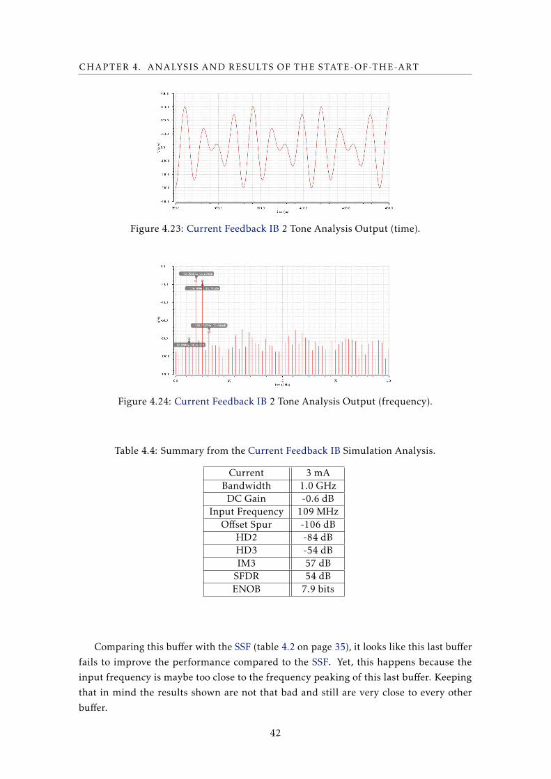
CHAPTER 4. ANALYSIS AND RESULTS OF THE STATE-OF-THE-ART
Figure 4.23: Current Feedback IB 2 Tone Analysis Output (time).
Figure 4.24: Current Feedback IB 2 Tone Analysis Output (frequency).
Table 4.4: Summary from the Current Feedback IB Simulation Analysis.
Current 3 mABandwidth 1.0 GHz
DC Gain -0.6 dBInput Frequency 109 MHz
Offset Spur -106 dBHD2 -84 dBHD3 -54 dBIM3 57 dB
SFDR 54 dBENOB 7.9 bits
Comparing this buffer with the SSF (table 4.2 on page 35), it looks like this last buffer
fails to improve the performance compared to the SSF. Yet, this happens because the
input frequency is maybe too close to the frequency peaking of this last buffer. Keeping
that in mind the results shown are not that bad and still are very close to every other
buffer.
42

4.5. VGS-CONTROLLED CASCADED SOURCE FOLLOWER INPUT BUFFER
4.5 Vgs-controlled Cascaded Source Follower Input Buffer
The Vgs-controlled CSF IB uses a negative feedback loop to reduce the Vgs variances of
each cascaded devices on the CSF design. This feedback loop is responsible to reduce the
impact of input-dependant Vgs variations on the circuit, increasing linearity.
4.5.1 DC Analysis (Vgs-controlled CSF IB)
For the sizing of the circuit, the main objective was to ensure the output current through
the NM1 device. All the currents and operating points of each device are shown in
figure 4.25. For linearity and bandwidth results, the current used in both branches of
the differential pair of PM5 and PM8 does not have the same current. Note that, even
though PM8 is not is a traditional common-drain topology, [26] recommends to remove
this device’s body-effect.
Figure 4.25: Vgs-controlled CSF IB DC Operating point.
It is reported in [26] the use of a compensation capacitor to increase the phase margin.
However, since the simulated results were under the reported behavior, this capacitor
was not used in these simulations.
4.5.2 AC Analysis (Vgs-controlled CSF IB)
The AC analysis of the Vgs-controlled CSF IB, shown in figure 4.26 shows that this design
also has a peaking at higher frequencies. However, this peaking is not as noticeable as
the Current Feedback IB’s. Furthermore, the DC Gain of this design is comparable to
the designs with one buffer stage, meaning that the feedback loop is also increasing the
overall design’s gain.
43

CHAPTER 4. ANALYSIS AND RESULTS OF THE STATE-OF-THE-ART
Figure 4.26: Vgs-controlled CSF IB Frequency Response.
The bandwidth value of this design, calculated by the point with a 3 dB decrease
compared to the DC value, is 1.2 GHz. The peaking is felt around frequencies of the 100
MHz range.
4.5.3 Transient-noise Analysis (Vgs-controlled CSF IB)
The transient-noise analysis did not present problems, considering that the DC gain of
this IB is comparable to every other one-staged buffer, the input voltage amplitude did
not stress the operating point of any device. Figure 4.27 shows the differential output
signal. Using an FFT the time domain signal was brought to the frequency domain, where
it is possible to look at the power of each frequency.
Figure 4.27: Vgs-controlled CSF IB Output (time).
The signal FFT is shown in figure 4.28. The marked frequencies are the fundamental
harmonic power, the second harmonic power, and the third harmonic power.
Setting up the 2 tone analysis and extracting the time wave presented no problem.
The maximum differential output swing was set up to 600 mV and the result is presented
in figure 4.29.
Checking the signal on frequency domain in figure 4.30, the same aspect as the other
designs appears with two clear power spikes at the fundamental harmonics frequencies.
In the next table 4.5 the results of the analysis are shown.
44
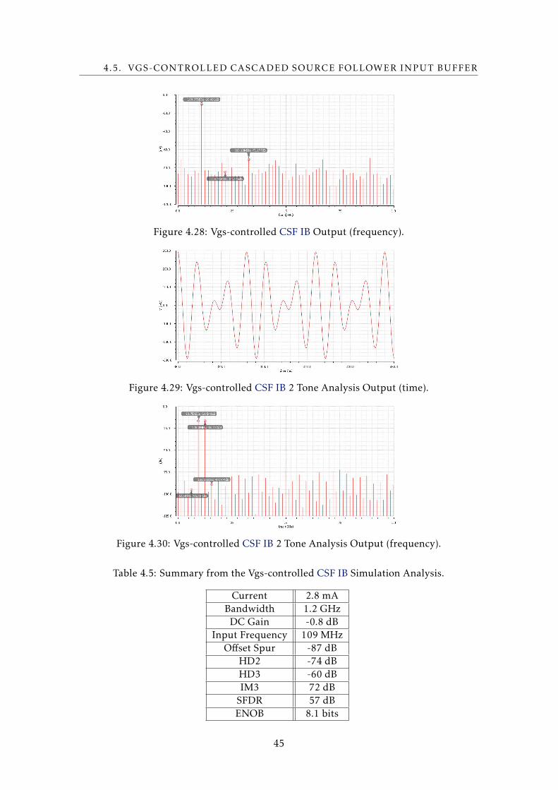
4.5. VGS-CONTROLLED CASCADED SOURCE FOLLOWER INPUT BUFFER
Figure 4.28: Vgs-controlled CSF IB Output (frequency).
Figure 4.29: Vgs-controlled CSF IB 2 Tone Analysis Output (time).
Figure 4.30: Vgs-controlled CSF IB 2 Tone Analysis Output (frequency).
Table 4.5: Summary from the Vgs-controlled CSF IB Simulation Analysis.
Current 2.8 mABandwidth 1.2 GHz
DC Gain -0.8 dBInput Frequency 109 MHz
Offset Spur -87 dBHD2 -74 dBHD3 -60 dBIM3 72 dB
SFDR 57 dBENOB 8.1 bits
45

CHAPTER 4. ANALYSIS AND RESULTS OF THE STATE-OF-THE-ART
Comparing this buffer with the CSF (table 4.3 on page 39) there are many similarities
between the two. One difference is regarding the bandwidth and the total current of the
devices. Since this one has uses less current and has one more feedback loop it is expected
that the bandwidth decreases as well. Another difference regards the DC Gain that, in
this architecture, is doubled than that of the CSF.
4.6 Summary of all the analyses
In this chapter, some buffers were tested in the same conditions. Now, a fair comparison
can be done between all of them. In table 4.6 such comparison is drawn.
Table 4.6: Comparison between tested designs analysis.
SF SSF CSFCurrent
FeedbackIB
Vgs-Controlled
CSF IBCurrent (mA) 2.0 2.6 4.0 3.0 2.8
Bandwidth (GHz) 1.5 1.7 1.6 1.0 1.2DC Gain (dB) -0.7 -0.8 -1.5 -0.6 -0.8
Input Frequency (MHz) 109 109 109 109 109Offset Spur (dB) -121 -105 -90 -106 -87
HD2 (dB) -80 -85 -73 -84 -74HD3 (dB) -55 -61 -56 -54 -60IM3 (dB) 70 66 59 57 72
SFDR (dB) 55 61 57 54 57ENOB (bits) 8.0 8.5 8.1 7.9 8.1
Regarding current, most of all simulated designs use around the 2.5 mA. The CSF is
the only one not on this mark, mostly because the first stage was not power-optimized
and was drawing 1 mA like the second stage.
Bandwidth wise, there was a major performance boost on the SSF. There still is the
problem regarding peaking on the SSF and Current Feedback IB designs. The was most
assuredly from some pole-zero frequency response that probably should need some more
study to prevent or minimize the effects without changing much of the current. Another
way to reduce this effect is by using some outside regulation.
The DC Gain of all topologies was similar and around -0.7 dB. Yet, the CSF had -1.5
dB gain. This difference is explained by the use of two different buffer stages, while every
other buffer had just one device in common mode configuration, the CSF had 2 devices.
By assuming that each device attenuates the output by 0.7 dB having a gain of around
-1.4 dB with 2 of these devices is expected. However, the Vgs-controlled CSF IB topology
does not have this problem, this happens because of the feedback loops in the design.
Regarding HD2, or any even harmonic distortion, no design was much affected by this.
The differential nature of the buffers reduces even harmonic distortion, as shown in this
analysis. HD3, and odd harmonic distortion, is a major concern not easily solvable. Out
46

4.6. SUMMARY OF ALL THE ANALYSES
of all of the tested designs, the best performance was achieved by the SSF, this might have
happened since it was the buffer with feedback that had the most output swing available.
The ENOB is mostly used for data converters. Yet, because the buffer will limit the
effectiveness of the ADC it is used here to have a better understanding of the efficiency
of the buffer. In this category, the best buffer is SSF while all the other four have pretty
similar results.
Comparing SFDR the best result comes from the SSF, which is not surprising since
this metric, in this case, would be mostly limited by the HD3, as it is possible to see in
the figures representing the spectrum of each tested design.
The next chapter presents a new buffer architecture and the ideas behind the design.
Furthermore, the proposed buffer will be subject to the same analysis done. Lastly, the
proposed design will suffer some improvements to maximize its performance.
47


Chapter
5Proposed Architecture
A new architecture is studied for a high-bandwidth and high-linearity IB. The main ideas
and schematic are presented briefly, followed by the simulation of the new IB and some
improvements. Lastly, at the end of this chapter, some comparisons are made between
this architecture and the state-of-the-art.
5.1 Circuit Schematic and Proposed Idea
The schematic of the proposed architecture, shown in figure 5.1, is based on some pre-
viously shown buffer architectures with two different feedback branches. Firstly the
transistors M1 and M2 form a cascaded source follower in which the two have a different
branch of feedback loops. The first feedback loop happens in the loop of M7, M8, M9,
and M4. If the voltage at the gate of M2 rises while V out is constant the Vgs of M2 rises
and the current increases. With that increase the drain of M2 will decrease, decreasing
as well the Vgs of M7 (VCASP is constant) and the current through M7. The decrease in
current in M7 will decrease the drain voltage that is the gate voltage on M4, meaning
that the Vgs decreases, its current decreases, and V out increases. This one serves as a
positive feedback loop to guarantee some bandwidth by quickly raising V out when the
input increases.
The second feedback loop starts from the voltage of the gate of M4 and M9 to M14.
Completing the example above, if the voltage at the gate of M14 decreases then the current
decreases, since Vgs decreases. This will increase the drain voltage of M14, which is the
same as the M5 gate voltage. The increase of the gate voltage will reduce Vgs, decreasing
the current and lowering the drain voltage of M5. The drain voltage of M5 is the gate
of M2 contrary to the supposed rise of the last paragraph, meaning that this is negative
feedback.
49

CHAPTER 5. PROPOSED ARCHITECTURE
Figure 5.1: Proposed Input Buffer Architecture.
The last two devices that need introduction are M10 and M11. These devices are
responsible to assure that M8 is always in the strong-inversion state.
5.2 DC Analysis
Since this buffer is the one with the most branches, it should be the one with the most
power drained out of all simulated. The sizing was done to have a current of 1 mA flowing
through M2, in accordance with the guidelines. There is no need to have a high current
flowing through M1. In this case the current was sized to be 350 µA.
The current feedback ratio in the first feedback loop was sized to be around 1/3 of
the current flowing through M2. This means that the current from M7 and M9 was set
to be around 333 µA. The higher this ratio the higher the bandwidth and the higher the
peaking at higher frequencies.
The second feedback loop was sized to be 1/1. This choice was made taking into
account that the results were better with a higher ratio and, since the current in M1 will
be lower compared to M2, it was decided that the same current could be used in this
feedback loop.
Moreover, M10 and M11 were set to drive M8 with a significantly higher current
so they were set to have 3mA. These values were simulated to have some significant
improvements on the bandwidth with minimal increases in the power needed for the
block. This current minimized the total peaking of the buffer.
50

5.3. AC ANALYSIS
Figure 5.2 shows the operating point that was used for the next simulations. Even
though the sizing of the transistors was achieved and every device is in the strong inver-
sion region, it is possible to see that there is no comfort range for most of the devices. One
way to increase this range would be to decrease the use of cascode devices. However, since
the desired operation point was achieved, it was decided to continue with said devices.
Figure 5.2: Operating point of proposed architecture.
Aside from that, there was caution in sizing M10 and M11, the devices used to bias
M8 into the strong-inversion region. If there was a small variance of the current between
the two of them then there would be the same variance between devices M7 and M9. The
said variance could have some negative impact on the buffer’s performance. As such,
devices M10 and M11 were sized to have the same current flowing through them.
5.3 AC Analysis
In this AC analysis, the study was divided into 3 stages. The first one refers to the
output/input of M1 controlled by the negative feedback, the second one refers to the
output/input of M2 controlled by the positive feedback and the last one refers to the full
buffer output/input.
Figure 5.3 represents the gain between the gate and the source of M2. This transfer
function is similar to the gain of the Current Feedback IB in figure 4.20 on page 40.
This trace represents the positive feedback and it is noticeable the peaking at a higher
frequency. With the sizing presented in figure 5.2 the bandwidth between the gate and
the source of M2 is about 2.6 GHz.
In figure 5.4 it is possible to see the outwards loop gain, between the gate and source
of M1. This trace is the first to have a "negative"peaking mostly because it is a negative
feedback loop. At the same higher frequency this loop will decrease the gain with a similar
effect to the previous one. In this loop, the bandwidth achieves around 7 GHz. However,
it is important to note that the node capacitance shouldn’t be that high considering that
51

CHAPTER 5. PROPOSED ARCHITECTURE
Figure 5.3: Gain on the positive feedback loop.
it is, essentially, the gate of M2. This assures the increase in bandwidth should increase,
since the load is smaller, which validates the assumption that the current through M1
does not need to be that high, compared to M2.
Figure 5.4: Gain on the negative feedback loop.
Figure 5.5 shows the two traces together and check that both peakings are achieved
at similar frequency ranges. This is a good aspect of this architecture since, if the sizing
is well achieved, the two peakings should cancel each other into a constant gain of the
buffer until the cutoff frequency.
The result of the total buffer is shown in figure 5.6, here the gain is mostly flat until
the cutoff frequency. The total bandwidth achieved is around 2.5 GHz. This means that
the negative feedback is controlling the positive feedback peaking, as was expected. It
is important to note that this value is smaller than any individual value of the stages,
however, the gain is, overall, flatter than any other.
52

5.4. TRANSIENT-NOISE ANALYSIS
Figure 5.5: Comparison between positive and negative feedback loop gains.
Figure 5.6: Proposed architecture frequency gain.
5.4 Transient-noise Analysis
The transient-noise analysis was used to calculate the linearity of the buffer. A single
tone input wave was used to determine the harmonic distortion of the system. In figure
5.7 the output sine wave is visible. This wave was aimed to have 600 mV peak-to-peak
differential voltage to be able to compare with all other buffers studied before.
The time wave was decomposed into all the frequency power FFT presented in figure
5.8. It’s possible to see the fundamental harmonic peak, in this figure. Besides, are
marked the 2nd and 3rd harmonics.
After the single tone analysis, the double-tone analysis was set and the process re-
peated. In figure 5.9 the time wave is shown as the output of the buffer when the input is
composed of two different frequency signals. The target was to have an output wave with
a maximum voltage of 600 mV peak-to-peak differential.
53

CHAPTER 5. PROPOSED ARCHITECTURE
Figure 5.7: Proposed architecture Output (time).
Figure 5.8: Proposed architecture Output (frequency).
Taking a look at the FFT of the previous signal, in figure 5.10 it is possible to see
the fundamental harmonics of the different signals. Even though it looks like the inter-
modulation is worst in this buffer compared to the previous ones, this is certainly not the
case, since the inter-modulation frequencies are, in fact, better, yet the reason why it is
fairly different from previous buffers is that most of the other frequencies got attenuated
even more and, for the sake of showing up all the calculated points on the FFT, the scale
is different on this one figure.
Lastly, in table 5.1 it’s compiled some results of the previous analysis.
54

5.4. TRANSIENT-NOISE ANALYSIS
Figure 5.9: Proposed architecture 2 Tone Analysis Output (time).
Figure 5.10: Proposed architecture 2 Tone Analysis Output (frequency).
Table 5.1: Summary from the Proposed Buffer Simulation Analysis.
Current 10 mABandwidth 2.3 GHz
DC Gain -2.0 dBInput Frequency 109 MHz
Offset Spur -96 dBHD2 -87 dBHD3 -53 dBIM3 68 dB
SFDR 53 dBENOB 7.9 bits
Regarding current, it is important to note that most of it (6 mA) comes from the extra
branch used to drive the cascoded NMOS. That branch can give more or less flatness to
55

CHAPTER 5. PROPOSED ARCHITECTURE
the overall frequency gain by increasing or decreasing the current, respectively.
The last point can improve bandwidth by flattening the gain until higher frequencies
but that would increase the power dissipation slightly.
In terms of linearity, the results were not as expected. That is why we made some
variations to try and get some better performances.
5.5 Proposed Buffer with Improvements
As stated in section 5.2 - DC Analysis, some devices are at almost barely in strong inver-
sion, and that some variation on the Vds of said devices would take them out of the strong
inversion, creating non-linearity issues. Trying to keep the same ideas behind the circuit,
figure 5.11 shows the last circuit changes compared to figure 5.1. The only difference is
that transistor M13 from 5.1 does not show up in figure 5.11.
Figure 5.11: Proposed Improved Input Buffer Architecture.
Regarding the buffer’s TF, it was used MSAAC to achieve some expression on the gain.
However, even with a high tolerance for expression errors, it proved to be too complex to
analyze. Yet, if we ignore the parasitic effect of every device, the DC Gain expression of
the circuit is found to be
DC Gain =gm1 · (gm4 + gm9)
gm1 · (gm4 + gm9) + gm4 · (gds1 + gds5) + gm9 · gds1, (5.1)
with 10% error. The DC Gain expression is affected by the first stage of the design, as it
will be reinforced in the following analysis. It is also possible to check that most of the
56

5.5. PROPOSED BUFFER WITH IMPROVEMENTS
corruption factor is dominated by gm4 meaning that, optimally, to achieve an ideal buffer
these values should be the smallest possible.
5.5.1 DC Analysis
Naturally, since most of the problems were regarding linearity, taking out the M13 device
proved to be a sound improvement. This device is a cascode for M12, responsible to
protect the drain of the latter against significant voltage variations. However, it is signifi-
cantly easier to remove than the M8 device. Since eliminating the latter one would mean
to lose the extra freedom from the boosted current.
With this changes it was possible to reduce the total current of the circuit. For this
DC operating point the current through M1 and M2 were unchanged, 350 µA and 1 mA
respectively. The current through M9 and M7 was lower to about 1/4 of M2’s current
value (i.e. 250 µA). The second feedback loop’s current was lower as well. It was chosen a
current feedback ratio of 1/3 meaning that the current flowing in M14 and M12 is about
116 µA. Lastly the current in M10 and M11 was lowered to 1 mA.
All these changes were done to achieve the best results of bandwidth and linearity
with the least possible total current. However, the same functions described earlier apply.
Meaning that the current through M2 was chosen because of the guidelines. M1’s current
was chosen to achieve a certain bandwidth. M7’s current was chosen for bandwidth and
peaking concerns. Finally, M11’s current was chosen to limit the total peaking of the
buffer.
In figure 5.12 the operating point of the buffer is shown. Note that the currents on
all branches have been further optimized to have the minimum necessary biasing current
for this buffer. In the end, with this simplification, it was possible to achieve the same
results with a little more than half of the previous power dissipation.
Figure 5.12: Operating point of proposed improved input buffer architecture.
57

CHAPTER 5. PROPOSED ARCHITECTURE
This change does improve current consumption. However, this is working with al-
most the absolute minimum to have a stable and improved performance. The linearity
performance is so noticeable that even with this low power budget it is relevant.
5.5.2 AC Analysis
Similarly, as with the first proposed architecture, the AC analysis was divided into three.
The first one refers to the first stage buffer by M1 device, the second one to the second
stage buffer by M2 device, and the last one with the total buffer.
Figure 5.13 represents the positive feedback loop gain. It has the peaking at high
frequency and a bandwidth of around 2.2 GHz. This peaking is the main reason why an
outside negative feedback loop is used.
Figure 5.13: Gain on the positive feedback loop (Improved).
The negative feedback loop TF is shown in figure 5.14. Here the peaking is negative
so that they would cancel each other when together. Since M1 only has to drive the gate
of M2 the bandwidth of this buffer is better, even though there is less current through M1
compared to M2. The bandwidth of this branch is 6.1 GHz.
For easy comparison between the two figures 5.13 and 5.14 were compiled together
in figure 5.15 where it is possible to confirm that both peakings are roughly at the same
frequency.
Figure 5.16 shows the buffer total TF. Note that this operation point flattens the
response much better than the one on figure 5.6 with the same current. This, again,
might be a reason to decrease the circuit’s biasing current. The overall bandwidth of the
system is 2.2 GHz.
So far the overall bandwidth is almost the same between designs, however, the im-
proved version does improve the flatness of the TF, making so that the buffer can have a
better performance at higher frequencies without a need for outside calibrations. If the
flatness is important then it is advised to consider increasing the current on devices PM4
58

5.5. PROPOSED BUFFER WITH IMPROVEMENTS
Figure 5.14: Gain on the negative feedback loop (Improved).
Figure 5.15: Comparison between positive and negative feedback loop gains.
and NM7 of figure 5.12 since higher currents on this branch tends to decrease the effect
of the total peaking.
5.5.3 Transient-noise Analysis
The transient-noise analysis followed the same pattern as all the previous ones. Firstly a
single tone input was used in a way to achieve a 600 mV peak-to-peak differential output
voltage. The output signal is presented in figure 5.17.
This wave, aside from confirming the output maximum level, does not provide much
information. It is necessary to use its FFT to extract some more information. Figure 5.18
shows the fundamental harmonic frequency as well as the second and third harmonic
power. In this, it is possible to see that both of these harmonic distortions got slightly
improved over figure 5.8.
59
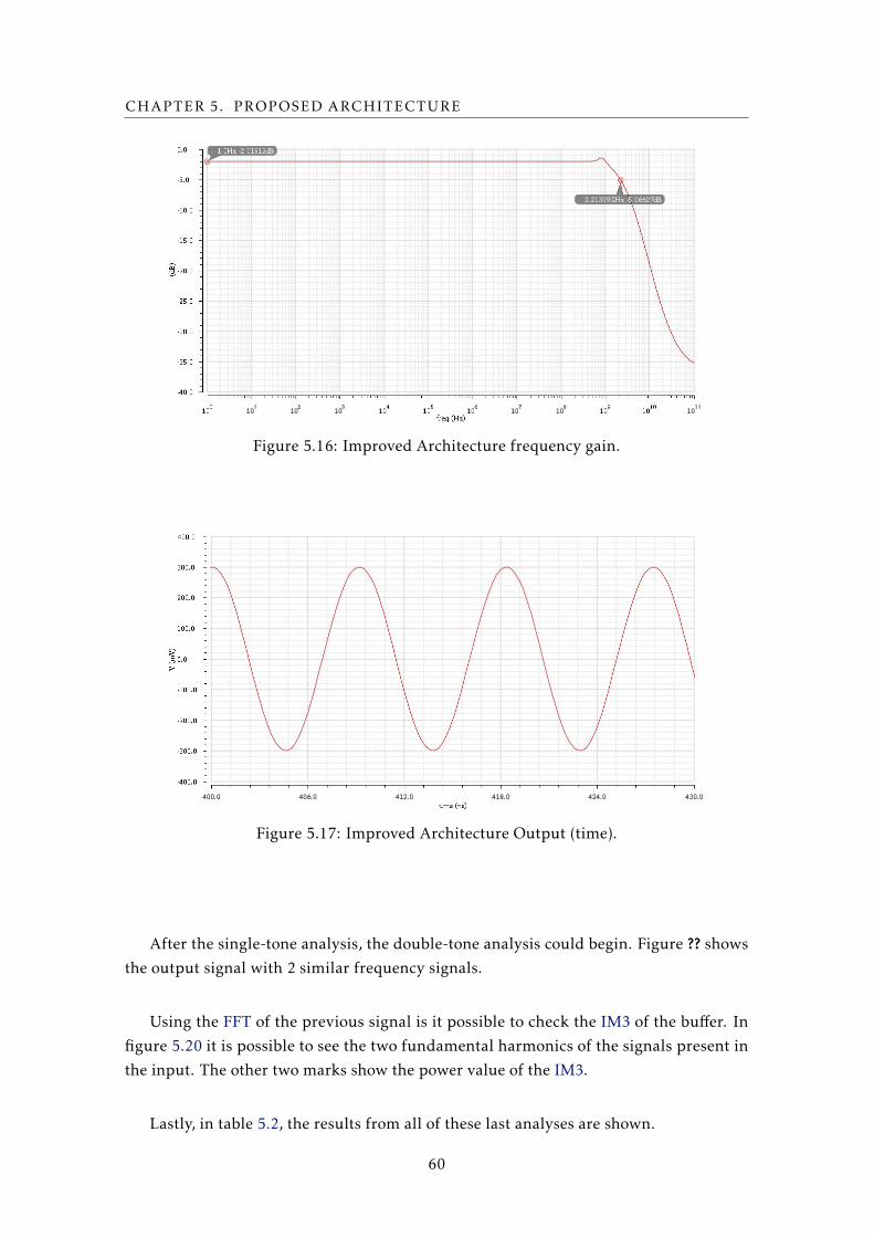
CHAPTER 5. PROPOSED ARCHITECTURE
Figure 5.16: Improved Architecture frequency gain.
Figure 5.17: Improved Architecture Output (time).
After the single-tone analysis, the double-tone analysis could begin. Figure ?? shows
the output signal with 2 similar frequency signals.
Using the FFT of the previous signal is it possible to check the IM3 of the buffer. In
figure 5.20 it is possible to see the two fundamental harmonics of the signals present in
the input. The other two marks show the power value of the IM3.
Lastly, in table 5.2, the results from all of these last analyses are shown.
60

5.5. PROPOSED BUFFER WITH IMPROVEMENTS
Figure 5.18: Improved Architecture Output (frequency).
Figure 5.19: Improved Architecture 2 Tone Analysis Output (time).
Table 5.2: Summary from the Improved Buffer Simulation Analysis.
Current 5.5 mABandwidth 2.2 GHz
DC Gain -2.0 dBInput Frequency 109 MHz
Offset Spur -95 dBHD2 -81 dBHD3 -66 dBIM3 65 dB
SFDR 66 dBENOB 9.3 bits
It is possible to see a noticeable improvement over the values on table 5.1. This
improvement certifies that there was too much strain on some of the first design’s devices.
61

CHAPTER 5. PROPOSED ARCHITECTURE
Figure 5.20: Improved Architecture 2 Tone Analysis Output (frequency).
Because the output needs to be at a predefined value besides this buffer having low DC
gain, it was necessary to have an input signal with high amplitude. The high input voltage
might have been responsible to cause all the non-linearity in the previous buffer.
Of course, since this one had such a better performance in both AC and transient-noise
analysis, it would be recommended to try and decrease the current supply further to make
it more competitive with the simulated buffers in chapter 4 - Analysis and Results of the
state-of-the-art. However, this simple change was made to improve the proposed buffer.
Table 5.3 shows the improvement without the cascoded transistor.
Table 5.3: Comparison between simulated designs analysis.
Proposed IB Proposed Improved IBCurrent 10 mA 5.5 mA
Bandwidth 2.3 GHz 2.2 GHzDC Gain -2.0 dB -2.0 dB
Input Frequency 109 MHz 109 MHzOffset Spur -96 dB -95 dB
HD2 -87 dB -81 dBHD3 -53 dB -66 dBIM3 68 dB 65 dB
SFDR 53 dB 66 dBENOB 7.9 bits 9.3 bits
It is possible to see that overall the improved proposed input buffer is 10 dB better
compared to the proposed buffer in terms of SFDR. While the power dissipated by the
improved design is about half of that of the first proposed design, both bandwidths are
pretty much the same.
The DC gain is the same in both input buffers and is mostly limited by the first stage
gain. Equation (5.1) shows that most of the DC gain depends just on the first stage
62

5.5. PROPOSED BUFFER WITH IMPROVEMENTS
meaning that, to improve the overall gain it is most important to improve the first stage
gain.
Linearity wise, the improved proposed buffer does have a better performance in all
regards. This design is not as restrained by the change of the voltage levels of the input.
However, in terms of IM3, the first proposed design does come out ahead but by a small
margin.
Still about linearity, the value of HD3 is lower than that of the Current Feedback IB
in table 4.4 in page 42. However, the value of HD2 is actually bigger than the value on
that same table. This indicates that the second feedback loop may improve HD3 while
degrading HD2 what, in this case, is preferable. The HD2 value will be attenuated since
it is used a differential input buffer.
In the next chapter, the comparison between these two architectures will be done
against all previous designs.
63


Chapter
6Conclusion
Over the course of the last two chapters, there was a series of simulations done to several
different buffer designs. In this chapter, the last comparisons will be drawn between all
studied designs. This chapter presents an overall conclusion on the work done, problems
faced, and future work that could be pursued to further improve this investigation.
6.1 Final Comparisons
In chapter 4 - Analysis and Results of the state-of-the-art - it was studied 4 different ar-
chitectures. They were the Source Follower (Section 4.1), Super Source Follower (Section
4.2), Cascaded Source Follower (Section 4.3) and Current Feedback IB (Section 4.4).
In chapter 5 - Proposed Architecture - a new buffer design was presented, as well as an
improvement more suited for low voltage supply.
At the end of both of these chapters was shown a table compiling the results of all of
the analyses to make an easy comparison between designs of the same chapter, however,
there was not a comparison between all the designs.
Table 6.1 shows all of the results into a single compacted table for easy comparison.
65
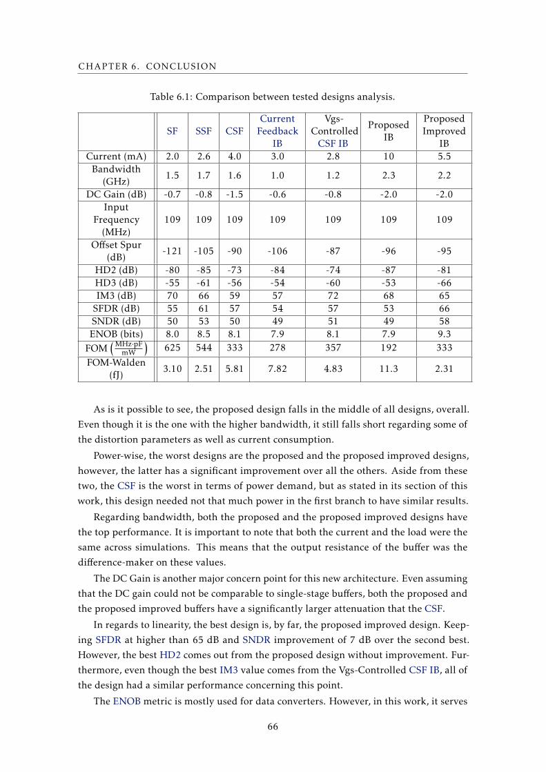
CHAPTER 6. CONCLUSION
Table 6.1: Comparison between tested designs analysis.
SF SSF CSFCurrent
FeedbackIB
Vgs-Controlled
CSF IB
ProposedIB
ProposedImproved
IBCurrent (mA) 2.0 2.6 4.0 3.0 2.8 10 5.5
Bandwidth(GHz)
1.5 1.7 1.6 1.0 1.2 2.3 2.2
DC Gain (dB) -0.7 -0.8 -1.5 -0.6 -0.8 -2.0 -2.0Input
Frequency(MHz)
109 109 109 109 109 109 109
Offset Spur(dB)
-121 -105 -90 -106 -87 -96 -95
HD2 (dB) -80 -85 -73 -84 -74 -87 -81HD3 (dB) -55 -61 -56 -54 -60 -53 -66IM3 (dB) 70 66 59 57 72 68 65
SFDR (dB) 55 61 57 54 57 53 66SNDR (dB) 50 53 50 49 51 49 58ENOB (bits) 8.0 8.5 8.1 7.9 8.1 7.9 9.3
FOM(MHz·pF
mW
)625 544 333 278 357 192 333
FOM-Walden(fJ)
3.10 2.51 5.81 7.82 4.83 11.3 2.31
As is it possible to see, the proposed design falls in the middle of all designs, overall.
Even though it is the one with the higher bandwidth, it still falls short regarding some of
the distortion parameters as well as current consumption.
Power-wise, the worst designs are the proposed and the proposed improved designs,
however, the latter has a significant improvement over all the others. Aside from these
two, the CSF is the worst in terms of power demand, but as stated in its section of this
work, this design needed not that much power in the first branch to have similar results.
Regarding bandwidth, both the proposed and the proposed improved designs have
the top performance. It is important to note that both the current and the load were the
same across simulations. This means that the output resistance of the buffer was the
difference-maker on these values.
The DC Gain is another major concern point for this new architecture. Even assuming
that the DC gain could not be comparable to single-stage buffers, both the proposed and
the proposed improved buffers have a significantly larger attenuation that the CSF.
In regards to linearity, the best design is, by far, the proposed improved design. Keep-
ing SFDR at higher than 65 dB and SNDR improvement of 7 dB over the second best.
However, the best HD2 comes out from the proposed design without improvement. Fur-
thermore, even though the best IM3 value comes from the Vgs-Controlled CSF IB, all of
the design had a similar performance concerning this point.
The ENOB metric is mostly used for data converters. However, in this work, it serves
66

6.1. FINAL COMPARISONS
as a metric for the performance of the design. Note that most of the buffers in these
conditions were pretty constant with 8 bits with the SSF coming off around with 8.5 bits
ENOB. The best one on this metric was once again the improved design with more than
9 bits ENOB.
The first Figure of Merit (FOM) was proposed in [15]. It describes a way of calculating
a FOM by relating the Product Gain Bandwidth (GBW) with the capacitive load and the
power dissipation of the OpAmp. In [15] it is used
GBW ·CL
P ower(6.1)
to calculate the value of this FOM. In this work, since the DC gain is around 0 dB instead
of using GBW we used BW. These values represent the efficiency of the block in term
of BW. In this case, the higher the value means better performance. Naturally, because
it had only one stage and had no feedback, the SF was the best design in this regard
followed by the SSF. Note that this FOM does not consider linearity.
The FOM-Walden is used to categorizing ADCs. However, since it takes into account
the linearity it was used here to categorize the buffer in terms of linearity. This FOM is
calculated byP ower
2SNDR−1.76
6.02 · 2 ·BW(6.2)
to account for the power, bandwidth, and linearity of the ADCs. Notice that, in case of
the Walden FOM, the lower the number the better the efficiency of the IB. Regarding its
values, the proposed improved IB has the best FOM-Walden.
Finally, the same simulations were done with some variation at the supply voltage.
These simulations serve the purpose of an overview of the variation of the buffer’s working
conditions. Table 6.2 represents the change of the supply voltage to less 10% of its original
value.
Table 6.2: Comparison between tested designs analysis (@ 1.08 V supply voltage).
SF SSF CSFCurrent
FeedbackIB
Vgs-Controlled
CSF IB
ProposedIB
ProposedImproved
IBBandwidth
(GHz)1.5 1.7 1.6 1.0 1.1 2.2 2.1
IM3 (dB) 67 59 51 59 65 57 61SFDR (dB) 55 58 49 53 57 50 59
ENOB (bits) 7.9 8.3 8.0 7.8 8.1 7.6 9.0
Overall all of the buffers suffered some degradation in their performance. This degra-
dation was more significant in complex designs like the Current Feedback IB and both
proposed architectures. Even though the improved buffer suffered the most degradation
in its performance, it is still the best buffer overall.
Continuing checking the variation at the supply voltage, Table 6.3 presents the results
with an increase of 10% of the supply voltage.
67

CHAPTER 6. CONCLUSION
Table 6.3: Comparison between tested designs analysis (@ 1.32 V supply voltage).
SF SSF CSFCurrent
FeedbackIB
Vgs-Controlled
CSF IB
ProposedIB
ProposedImproved
IBBandwidth
(GHz)1.5 1.8 1.6 1.0 1.3 2.4 2.3
IM3 (dB) 67 67 66 56 72 68 65SFDR (dB) 55 60 54 54 58 56 64
ENOB (bits) 8.0 8.4 8.0 7.9 8.2 8.0 9.3
With the increase of the supply voltage every buffer had some minor performance
improvement. Note that the biggest change was Vgs-Controlled CSF IB IM3 improvement,
however the SFDR on that buffer did not improve by the same rate, none the less this
buffer was the one with an overall performance improvement with higher supply voltages.
6.2 Final conclusion of the work
In summary, the proposed improved design looks like a functional input buffer design
for high linearity and high bandwidth purposes. It is important to note that the proposed
improved buffer had such performance on this technology (130 nm) with the constraints
labeled on table 3.1 on page 21. This means that in different technologies the proposed
buffers can have some distinct performances. However, it is possible to predict that
there should be some advantages of using more recent buffer designs in new technologies,
mainly regarding bandwidth and die area.
One final note, most of the buffers used in the industry do not follow the guidelines
of this work and usually are supplied with a voltage higher than the core voltage of the
technology. The higher voltage improves the performance of the buffer, as seen comparing
tables 6.1 and 6.3. However, this work was used to compare buffers with core devices.
Using core devices improves the speed of the buffer and eliminates the need for higher
voltages.
As a continuation of this work, further analysis of both proposed and proposed im-
proved designs in deep nanoscale technologies to investigate if these designs scale better
into newer FinFET and FD-SOI technologies.
68

Bibliography
[1] A. Bevilacqua and A. M. Niknejad. “An ultra-wideband CMOS LNA for 3.1 to 10.6
GHz wireless receivers.” In: 2004 IEEE International Solid-State Circuits Conference(IEEE Cat. No.04CH37519). 2004, 382–533 Vol.1. doi: 10.1109/ISSCC.2004.
1332754.
[2] Bo-Yang Chang and C. F. Jou. “Design of a 3.1-10.6GHz low-voltage, low-power
CMOS low-noise amplifier for ultra-wideband receivers.” In: 2005 Asia-Pacific Mi-crowave Conference Proceedings. Vol. 2. 2005, 4 pp. doi: 10.1109/APMC.2005.
1606458.
[3] F. Bruccoleri, E. A. M. Klumperink, and B. Nauta. “Noise cancelling in wideband
CMOS LNAs.” In: 2002 IEEE International Solid-State Circuits Conference. Digest ofTechnical Papers (Cat. No.02CH37315). Vol. 1. 2002, 406–407 vol.1. doi: 10.1109/
ISSCC.2002.993104.
[4] J. Carrillo, M. Dominguez, F. Duque, and G. Torelli. “Low-voltage wide-swing fully
differential CMOS voltage buffer.” In: Aug. 2011, pp. 122–125. doi: 10.1109/
ECCTD.2011.6043292.
[5] R. G. Carvajal, J. Ramirez-Angulo, A. J. Lopez-Martin, A. Torralba, J. A. G. Galan, A.
Carlosena, and F. M. Chavero. “The flipped voltage follower: a useful cell for low-
voltage low-power circuit design.” In: IEEE Transactions on Circuits and Systems I:Regular Papers 52.7 (2005), pp. 1276–1291. issn: 1558-0806. doi: 10.1109/TCSI.
2005.851387.
[6] P. Costa, C. Fiocchi, U. Gatti, and F. Maloberti. “High-performance BiCMOS output
buffer design strategies.” In: 1999 IEEE International Symposium on Circuits andSystems (ISCAS). Vol. 2. 1999, 168–171 vol.2. doi: 10.1109/ISCAS.1999.780645.
[7] C. Erdmann, E. Cullen, D. Brouard, R. Pelliconi, B. Verbruggen, J. Mcgrath, D.
Collins, M. De La Torre, P. Gay, P. Lynch, P. Lim, A. Collins, and B. Farley. “16.3
A 330mW 14b 6.8GS/s dual-mode RF DAC in 16nm FinFET achieving -70.8dBc
ACPR in a 20MHz channel at 5.2GHz.” In: 2017 IEEE International Solid-StateCircuits Conference (ISSCC). 2017, pp. 280–281. doi: 10 . 1109 / ISSCC . 2017 .
7870370.
69

BIBLIOGRAPHY
[8] Fan You, S. H. K. Embabi, and E. Sanchez-Sinencio. “Low-voltage class AB buffers
with quiescent current control.” In: IEEE Journal of Solid-State Circuits 33.6 (1998),
pp. 915–920. doi: 10.1109/4.678659.
[9] F. A. Farag. “High performance CMOS buffer amplifier with offset cancellation.”
In: 2013 Saudi International Electronics, Communications and Photonics Conference.
2013, pp. 1–4. doi: 10.1109/SIECPC.2013.6551015.
[10] A. Glascott-Jones, N. Chantier, F. Bore, and M. Wingender. “Direct conversion
techniques for radar systems.” In: 2013 14th International Radar Symposium (IRS).Vol. 1. 2013, pp. 288–295.
[11] A. Glascott-Jones, N. Chantier, F. Bore, M. Wingender, O. Gentaz, and M. Torres.
“High speed ADCs for direct conversion techniques in array radar systems.” In:
2013 IEEE International Symposium on Phased Array Systems and Technology. 2013,
pp. 69–73. doi: 10.1109/ARRAY.2013.6731801.
[12] P. R. Gray, R. G. Meyer, P. J. Hurst, and S. H. Lewis. Analysis and Design of AnalogIntegrated Circuits. 4th. USA: John Wiley & Sons, Inc., 2001. isbn: 0471321680.
[13] Y. Ha, M. Li, and A. Q. Liu. “Low-voltage high driving capability CMOS buffer
used in MEMS interface circuits.” In: ICECS’99. Proceedings of ICECS’99. 6th IEEEInternational Conference on Electronics, Circuits and Systems (Cat. No. 99EX357).Vol. 3. IEEE. 1999, pp. 1313–1316.
[14] B. Hershberg, D. Dermit, B. v. Liempd, E. Martens, N. Markulic, J. Lagos, and J.
Craninckx. “3.1 A 3.2GS/s 10 ENOB 61mW Ringamp ADC in 16nm with Back-
ground Monitoring of Distortion.” In: 2019 IEEE International Solid- State CircuitsConference - (ISSCC). 2019, pp. 58–60. doi: 10.1109/ISSCC.2019.8662290.
[15] Hiok-Tiaq Ng, R. M. Ziazadeh, and D. J. Allstot. “A multistage amplifier technique
with embedded frequency compensation.” In: IEEE Journal of Solid-State Circuits34.3 (1999), pp. 339–347. doi: 10.1109/4.748185.
[16] I. Hwang, D. Kim, J. Roh, M. Lee, S. Nah, and M. Song. “An 8-b cascaded folding
A/D converter with a new fully differential source follower.” In: 2013 EuropeanConference on Circuit Theory and Design (ECCTD). 2013, pp. 1–4.
[17] Joongsik Kih, Byungsoo Chang, and Deog-Kyoon Jeong. “Class-AB large-swing
CMOS buffer amplifier with controlled bias current.” In: IEEE Journal of Solid-StateCircuits 28.12 (1993), pp. 1350–1353. doi: 10.1109/4.262009.
[18] Y. Kong, S. Xu, and H. Yang. “An Ultra Low Output Resistance and Wide Swing
Voltage Follower.” In: 2007 International Conference on Communications, Circuitsand Systems. 2007, pp. 1007–1010. doi: 10.1109/ICCCAS.2007.4348217.
[19] E. Ozalevli, M. Qureshi, and P. Hasler. “Low-voltage floating-gate CMOS buffer.”
In: June 2006, 4 pp. –1875. doi: 10.1109/ISCAS.2006.1692974.
70

BIBLIOGRAPHY
[20] J. Ramirez-Angulo, R. G. Carvajal, A. Torralba, J. Galan, A. P. Vega-Leal, and J.
Tombs. “The flipped voltage follower: a useful cell for low-voltage low-power
circuit design.” In: 2002 IEEE International Symposium on Circuits and Systems.Proceedings (Cat. No.02CH37353). Vol. 3. 2002, pp. III–III. doi: 10.1109/ISCAS.
2002.1010299.
[21] H. Rapakko and J. Kostamovaara. “On the Performance and Use of an Improved
Source–Follower Buffer.” In: IEEE Transactions on Circuits and Systems I: RegularPapers 54.3 (2007), pp. 504–517. issn: 1558-0806. doi: 10.1109/TCSI.2006.
887609.
[22] B. Razavi. Fundamentals Of Microelectronics. 2nd. USA: John Wiley & Sons, Inc.,
2014.
[23] A. Tanaka, H. Kodama, and A. Kasamatsu. “Low noise amplifier with center fre-
quency hoping for an MB-OFDM UWB receiver.” In: June 2004, pp. 420 –423. isbn:
0-7803-8373-7. doi: 10.1109/UWBST.2004.1321008.
[24] B. Vaz, A. Lynam, B. Verbruggen, A. Laraba, C. Mesadri, A. Boumaalif, J. Mcgrath,
U. Kamath, R. De Le Torre, A. Manlapat, D. Breathnach, C. Erdmann, and B. Farley.
“16.1 A 13b 4GS/s digitally assisted dynamic 3-stage asynchronous pipelined-SAR
ADC.” In: 2017 IEEE International Solid-State Circuits Conference (ISSCC). 2017,
pp. 276–277. doi: 10.1109/ISSCC.2017.7870368.
[25] Xianping Fan and P. K. Chan. “Analysis and design of low-distortion CMOS source
followers.” In: IEEE Transactions on Circuits and Systems I: Regular Papers 52.8
(2005), pp. 1489–1501. issn: 1558-0806. doi: 10.1109/TCSI.2005.851711.
[26] G. Xing, S. H. Lewis, and T. R. Viswanathan. “A Unity-Gain Buffer with Reduced
Offset and Gain Error.” In: IEEE Custom Integrated Circuits Conference 2006. 2006,
pp. 825–828. doi: 10.1109/CICC.2006.320831.
[27] A. Zhuk, A. Bugakova, E. Ovsepyan, and N. Dmitriyenko. “The Complementary
Buffer Amplifiers with Low Static Current Consumption for Low-Voltage Analog
Microcircuits.” In: June 2018, pp. 86–89. doi: 10.1109/EDM.2018.8435041.
71