development and design
TRANSCRIPT


The Hong Kong Polytechnic University
Department of Electronic and Information Engineering
Development and Design
of
Light-emitting-diode (LED) Lighting
Power Supplies
Xiaohui QU
A thesis submitted in partial fulfillment of the requirements for
the degree of Doctor of Philosophy
November 2009

CERTIFICATE OF ORIGINALITY
I hereby declare that this thesis is my own work and that, to the best of my
knowledge and belief, it reproduces no material previously published or written,
nor material that has been accepted for the award of any other degree or diploma,
except where due acknowledgement has been made in the text.
(Signed)
Xiaohui QU (Name of Student)

To my family

Abstract
Light-emitting-diode (LED) light sources, which are more compact, capable
to change color in real time, less dissipative and more durable, are finding more
applications than conventional light bulbs in domestic, commercial and indus-
trial environments. However, LEDs have nonlinear optical, thermal and electri-
cal characteristics, which are major hurdles for widespread lighting applications.
Specifically, stabilizing colors of LED lights is a challenging task, which includes
color light intensity control using switching mode power converters, color point
maintenance against LED junction temperature change, and limiting LED device
temperature to prolong LED lifetime. Also, requirements such as high power
factor, long lifetime, accurate current control and high efficiency pose challenges
to the design of LED ballast circuits.
This thesis is devoted to the study and design of effective LED lighting
systems to overcome the inherent deficiencies and provide solutions for modern
lighting applications. The main contributions of this thesis are summarized as
follows:
1. To stabilize the colors of LED lights, we present an LED junction temper-
ature measurement technique for a pulse-width-modulation (PWM) diode
forward current controlled red, green and blue (RGB) LED lighting system.
The technique has been automated and can stabilize the color effectively
without the need for using expensive feedback systems involving light sen-
sors. Performance in terms of chromaticity and luminance stability for a
i

temperature compensated RGB LED system will be presented.
2. LED light sources have a long life expectancy. The lifetime of LED lumi-
naires are thus determined by their electronic ballasts. It is found that the
lifetime of power converters is limited by the high-voltage electrolytic ca-
pacitors which normally have the shortest lifetime compared to other com-
ponents in the system. A first-stage isolated power-factor-correction (PFC)
pre-regulator is proposed, which allows the storage capacitor to be located
in the secondary side of the isolation transformer. Low-voltage large ca-
pacitors of longer lifetime can therefore be used to extend the overall life-
time of the LED luminaires. Steady-state state-space averaging analysis is
performed for designing the converter in discontinuous conduction mode
(DCM). A prototype converter is built to verify performance of the pro-
posed PFC LED pre-regulator.
3. The concept of secondary capacitors is extended to operate the same PFC
pre-regulator in continuous conduction mode (CCM) for high-power ap-
plications (> 300 W). The arrangement of power delivery is identified as
the first non-cascading structure. Two secondary transformer windings and
a post LED current driver are arranged to form a second non-cascading
structure to improve efficiency. Additional buck current drivers can be
connected in parallel to drive more LEDs independently. Since the energy
from one output winding can directly be used to drive the LED without
going through another power stage, a higher efficiency can be guaranteed.
4. In applications with power lower than 25 W, the current harmonics require-
ments are less stringent as stated in some international standards. A high-
step-down-ratio and high-efficiency resonant assisted buck converter for
LED light sources is proposed, which also has the lifetime of capacitor
extended. The circuit is simple and efficient, without using isolation trans-
formers. Analysis and experimental verification are presented.
ii

Publications
Journal Papers
1. Xiaohui Qu, S. C. Wong, and Chi K. Tse, “Resonant assisted buck con-
verter for offline driving of high brightness LED replacement lamps,” sub-
mitted to IEEE Transactions on Power Electronics.
2. Xiaohui Qu, S. C. Wong, and Chi K. Tse, “Current-fed isolated PFC pre-
regulator for multiple LED lamps with extended lifetime,” submitted to
IEEE Transactions on Power Electronics.
3. Xiaohui Qu, S. C. Wong, and Chi K. Tse, “Non-cascading structure for
electronic ballast design for multiple LED lamps with independent bright-
ness control,” IEEE Transactions on Power Electronics, vol. 25, no. 2, pp.
331-340, Feb. 2010.
4. Xiaohui Qu, S. C. Wong, and Chi K. Tse, “Temperature measurement tech-
nique for stabilizing light output of RGB LED lamps,” IEEE Transactions
on Instrumentation and Measurement, vol. 59, no. 3, pp. 661-670, Mar.
2010.
iii
Conference Papers
1. Xiaohui Qu, S. C. Wong, and Chi K. Tse, “Resonant assisted buck con-
verter for offline driving of high brightness LED replacement lamps,” sub-
mitted to IEEE Energy Conversion Congress and Exposition (ECCE), 2010.
2. Xiaohui Qu, S. C. Wong, and Chi K. Tse, “Ballast for independent bright-
ness control of multiple LED lamps,” in Proceedings of IEEE Energy Con-
version Congress and Exposition (ECCE), pp. 2821-2826, Sep. 2009, San
Jose, USA.
3. Xiaohui Qu, S. C. Wong, and Chi K. Tse, “Electronic ballast for multiple
LED lamps with independent brightness control,” in Proceedings of IEEE
International Symposium on Circuits and Systems (ISCAS), pp. 2878-2881,
May 2009, Taipei, Taiwan.
4. Xiaohui Qu, S. C. Wong, and Chi K. Tse, “Isolated PFC pre-regulator
for LED lamps,” in Proceedings of IEEE Industrial Electronics Society
(IECON), pp. 1980-1987, Nov. 2008, Orlando, USA.
5. Xiaohui Qu, S. C. Wong, and Chi K. Tse, “Color control system for RGB
LED light sources using junction temperature measurement,” in Proceed-
ings of IEEE Industrial Electronics Society Conference (IECON), pp. 1363-
1368, Nov. 2007, Taipei, Taiwan.
iv

Acknowledgements
It is my pleasure and honor to have pursued my Ph.D. degree program at
the Hong Kong Polytechnic University. Time flies fast and it now comes to the
end of my Ph.D. period. In the past three years, it has been full of challenges,
happiness and achievements in both my study and life. This has been a special,
valuable and memorable experience for me.
First of all, I would like to thank Dr. Siu-Chung Wong and Prof. Michael
Tse, my supervisors, for their patient guidance, valuable advices and sustained
encouragement throughout the course of my candidature. Without their endless
support, I can not finish my Ph.D. study and submit the thesis successfully. Their
profound knowledge and immense enthusiasm on research impress me deeply. It
is wonderful to work with them and discussion with them always benefits me.
I would also like to thank Dr. Martin Chow, Dr. Y. M. Lai, Dr. S. C. Tan,
Prof. X. Ruan, Dr. Q. Chen, Dr. Herbert Iu for their kind suggestions on my
research. At the same time, I wish to thank all the colleagues in the Applied
Nonlinear Circuits and Systems Research Group and the friends I met in Hong
Kong. They include Xi Chen, Zhen Li, Yuehui Huang, Sufen Chen, Ming Li,
Jie Zhang, Ruoxi Xiang, Junfeng Sun, Xiumin Li, Xiujuan Zheng, Ada Zheng,
Grace Chu, Alan Lun, Song Xiong, Guorong Zhu, Xiaofan Liu, Qingfeng Zhou,
Ben Cheng, Martin Cheung, Kam-cheung Tam and Anson Lo. The time with you
will never be forgotten.
v

I gratefully acknowledge my host supervisor Prof. Fred. C. Lee for his guid-
ance during my study at the Virginia Polytechnic and State University. I would
like to thank Prof. D. Boroyevich and Dr. S. Wang for significant discussions.
Thanks also go to the members at the Center for Power Electronics Systems for
their help and friendship.
I sincerely thank The Hong Kong Polytechnic University for the financial
support of my study.
Last, but far from the least, special thanks go to my parents, my sister, and
my cute nephew, Ming Xin. I am deeply grateful for their persistent love and
constant care over the years.
Thank you!
vi

Contents
Abstract i
List of Publications iii
Acknowledgements v
Abbreviations xxii
Nomenclature List xxiii
1 Introduction 1
1.1 Motivation . . . . . . . . . . . . . . . . . . . . . . . . . . . . . 1
1.2 Literature Review . . . . . . . . . . . . . . . . . . . . . . . . . 7
1.2.1 LED Color Control and Dimming Methods . . . . . . . 7
1.2.2 Power Converters for LEDs . . . . . . . . . . . . . . . 10
1.3 Objective of the Thesis . . . . . . . . . . . . . . . . . . . . . . 12
1.4 Outline of the Thesis . . . . . . . . . . . . . . . . . . . . . . . 13
vii

2 Basics of LEDs 15
2.1 Physical Principle of LEDs . . . . . . . . . . . . . . . . . . . . 15
2.2 Materials for LEDs . . . . . . . . . . . . . . . . . . . . . . . . 18
2.3 Opto-Electrical Properties of LEDs . . . . . . . . . . . . . . . . 18
2.3.1 Current-Voltage Characteristic . . . . . . . . . . . . . . 19
2.3.2 Luminous Flux Emission . . . . . . . . . . . . . . . . . 20
2.3.3 Light Spectrum Characteristic . . . . . . . . . . . . . . 23
2.3.4 Lifetime and Failure . . . . . . . . . . . . . . . . . . . 23
2.4 Color and White Light with LEDs . . . . . . . . . . . . . . . . 24
2.5 Requirements for LED Luminaires . . . . . . . . . . . . . . . . 29
2.6 Summary . . . . . . . . . . . . . . . . . . . . . . . . . . . . . 31
3 Light Color Stabilization Using Temperature Measurement Technique 33
3.1 Introduction . . . . . . . . . . . . . . . . . . . . . . . . . . . . 33
3.2 Overview of RGB LED Color Control . . . . . . . . . . . . . . 34
3.3 Technique of Junction Temperature Compensation and Experi-
mental Measurements . . . . . . . . . . . . . . . . . . . . . . . 36
3.4 Implementation of RGB LED Junction Temperature Measure-
ment Technique in Light Color Stabilization . . . . . . . . . . . 41
3.5 Evaluation . . . . . . . . . . . . . . . . . . . . . . . . . . . . . 49
3.6 Summary . . . . . . . . . . . . . . . . . . . . . . . . . . . . . 51
viii

4 Electronic Ballasts for Multiple LED Lamps with Independent Bright-
ness Control 52
4.1 Introduction . . . . . . . . . . . . . . . . . . . . . . . . . . . . 52
4.2 Limitations of Conventional PFC Regulator in Converting En-
ergy Through High Leakage Inductance Transformer . . . . . . 54
4.3 PFC Current Regulator for LED Lamps . . . . . . . . . . . . . 55
4.4 Analysis and Implementation of the New PFC Pre-Regulator . . 57
4.4.1 Steady-State Waveforms . . . . . . . . . . . . . . . . . 57
4.4.2 Basic Assumptions for State-space Averaging . . . . . . 63
4.4.3 Averaging Over Converter Switching Frequency . . . . 64
4.4.4 Small-Signal Response of the Converter . . . . . . . . . 67
4.4.5 Dynamics Near Line Frequency . . . . . . . . . . . . . 68
4.5 Experimental Evaluation . . . . . . . . . . . . . . . . . . . . . 73
4.6 Summary . . . . . . . . . . . . . . . . . . . . . . . . . . . . . 79
5 Non-cascading Structure for Electronic Ballasts 80
5.1 Introduction . . . . . . . . . . . . . . . . . . . . . . . . . . . . 80
5.2 PFC Pre-Regulator Operating in CCM . . . . . . . . . . . . . . 82
5.3 Analysis and Implementation of Non-Cascading Output Config-
uration . . . . . . . . . . . . . . . . . . . . . . . . . . . . . . . 86
5.3.1 Theoretical Analysis for Efficiency Improvement . . . . 86
5.3.2 Optimization with Independent Brightness Control . . . 87
ix

5.3.3 Extension to More Structures . . . . . . . . . . . . . . . 92
5.4 Experimental Evaluation . . . . . . . . . . . . . . . . . . . . . 93
5.5 Summary . . . . . . . . . . . . . . . . . . . . . . . . . . . . . 101
6 Resonant Assisted Buck Converter for Low-power Lighting Applica-
tions 102
6.1 Introduction . . . . . . . . . . . . . . . . . . . . . . . . . . . . 102
6.2 Overview of the Resonant Assisted Buck Converter . . . . . . . 104
6.3 Analysis and Implementation . . . . . . . . . . . . . . . . . . 105
6.3.1 Operation Near Switching Frequency . . . . . . . . . . 106
6.3.2 Converter Design for Line Frequency Operation . . . . . 112
6.3.3 Design Procedures and Implementation of the Converter 112
6.4 Experimental Evaluation . . . . . . . . . . . . . . . . . . . . . 114
6.5 Summary . . . . . . . . . . . . . . . . . . . . . . . . . . . . . 119
7 Conclusion 121
7.1 Contributions of the Thesis . . . . . . . . . . . . . . . . . . . . 121
7.2 Suggestions for Future Work . . . . . . . . . . . . . . . . . . . 123
Bibliography 139
x

List of Figures
1.1 Comparison of luminous efficacy among different types of light-
ing devices. . . . . . . . . . . . . . . . . . . . . . . . . . . . . 2
1.2 Distribution of electricity energy utilization in the U.S. in 2008 . 3
1.3 Global market share 10 year forecast for lighting . . . . . . . . 4
1.4 Various LED lamps from different manufacturers. . . . . . . . . 4
1.5 Examples of commercial luminaires . . . . . . . . . . . . . . . 5
2.1 Effects of bias at the p-n junction of LED. . . . . . . . . . . . . 16
2.2 Forward current v.s. forward voltage of Lamina BL-4000 RGB
LEDs at 25 C ambient temperature. For each color, LEDs have
2 diodes connected in series [1]. . . . . . . . . . . . . . . . . . 20
2.3 Forward current v.s. forward voltage of red Lamp in the pack-
age of Lamina NT-43F0-0424 RGB LEDs at different heat sink
temperatures [2]. . . . . . . . . . . . . . . . . . . . . . . . . . 20
2.4 Luminous flux v.s. forward current of Lamina NT-43F0-0424
RGB LEDs at junction temperature Tj = 25 C [2]. . . . . . . . 22
2.5 Normalized flux v.s. junction temperature of Lamina NT-43F0-
0424 RGB LEDs at forward current IF = 350 mA [2]. . . . . . . 22
xi

2.6 Dominant wavelength shift of Seoul Semi Z-Power LEDs [3]. (a)
Dominant wavelength shift v.s. junction temperature at forward
current IF = 350 mA. (b) Dominant wavelength shift v.s. forward
current at ambient temperature TA = 25 C. . . . . . . . . . . . 24
2.7 Useful lifetime of an Lumileds Luxeon K2 white LED [4]. (a)
For different junction temperatures at IF = 1.5 A. (b) For different
forward currents at Tj = 125 C. . . . . . . . . . . . . . . . . . 25
2.8 CIE 1976 (u′, v′) chromaticity diagram. The outer curved bound-
ary is the monochromatic locus with wavelengths shown in nanome-
ters. . . . . . . . . . . . . . . . . . . . . . . . . . . . . . . . . 27
3.1 Color coordinates of typical LED of center wavelengths rang-
ing from 700 nm to 380 nm. Adjacent dots are separated by 5
nm in center wavelength. LEDs with center wavelengths of 624
nm (red), 525 nm (green) and 465 nm (blue) can generate color
points such as white, light red, light green and light blue within
the triangle shown in this figure. . . . . . . . . . . . . . . . . . 35
xii

3.2 Experimental light tristimulus X versus diode voltage (digital)
of (a) red LED light, (b) green LED light and (c) blue LED light
at different duty cycles. Diamonds, circles and triangles are data
points for X , Y and Z respectively and lines are fitted with the
data points. Duty cycles are descending from top to bottom with
d = 1.0 to d = 0.4 respectively for each component in X . Note
that Z in X of red light is almost zero and not shown in this fig-
ure. (d) gives relationships between actual (two diodes in series
connection) diode forward voltage and digital temperature Vdi for
i = r, g, b. The data points in (d) are measured using heat sink
temperature as variation parameter ranging from 20 C to 75 C
in obtaining the corresponding diode forward voltages (junction
temperatures). . . . . . . . . . . . . . . . . . . . . . . . . . . . 38
3.3 Evaluation of color points of the LEDs with center wavelengths
of 624 nm (red), 525 nm (green) and 465 nm (blue), marked
with small diamonds, changing with different heat sink tempera-
tures for a constant current driven (a) red (b) blue and (c) green
LEDs. Lines are least-square-fits of data points using second de-
gree polynomials. Shown in (d) are corresponding drifts of color
points relative to the color point at heat sink temperature of 30C. Note that the color space of CIE 1976 uniform chromaticity
scale is used here to give an even perceptual color difference. . . 39
3.4 Switching converter with PWM control as constant current driver. 41
3.5 Schematic of the RGB LED color control system. . . . . . . . . 42
3.6 LED lamp with LED microcontroller system which is composed
of three PWM current drivers and PIC18F1320 control circuitries. 42
3.7 LED diode forward voltage waveforms; upper trace for red LED,
middle trace for green LED and lower trace for blue LED. . . . 43
xiii

3.8 Functional block “level and gain adjustment” of Fig. 3.5. . . . . 43
3.9 Comparison of digital diode forward voltage Vdi and heat sink
temperature. The LEDs are driven by PWM current of 330 mA
and duty cycle of d = 0.8. Heat sink temperature is externally
controlled for a step change from 25 C to 35 C at t = 9 s. . . . 44
3.10 Comparison of digital diode forward voltage Vdi and heat sink
temperature. The sampled digital diode forward voltages are shown
as dots and the lines superimposed with the dots are calculated
using Eq. (3.7). The LEDs are driven by PWM current of 330
mA and duty cycle of d = 0.5. Heat sink temperature is kept at 25C while a step change from d = 0.5 to d = 0.8 is applied to the
blue channel. . . . . . . . . . . . . . . . . . . . . . . . . . . . 45
3.11 Automatic measurement and calibration suite. . . . . . . . . . . 45
3.12 Evaluation of output color points, marked as small diamonds,
changing with different heat sink temperatures for set-point col-
ors at (a) light red (b) light blue (c) light green and (d) D65
white, marked as small triangles. Lines are least-square-fits of
data points using second degree polynomials. . . . . . . . . . . 46
3.13 Evaluation of output brightness difference in Y value, correspond-
ing to Fig. 3.12. Data points triangles, squares, and circles are for
D65 white, light blue and light red respectively with set point at
Y = 2600. Data points diamonds are for light green with set point
at Y = 2000 and Y-axis at the right. Lines are least-square-fits of
data points using second degree polynomials. . . . . . . . . . . 48
xiv

3.14 Evaluation of output color difference using ∆u′v′, corresponding
to Fig. 3.12. Data points triangles, squares, circles, and diamonds
are for D65 white, light blue, light red and light green respec-
tively shown in Fig. 3.1. Lines are least-square-fits of data points
using second degree polynomials. . . . . . . . . . . . . . . . . 48
3.15 Evaluation of (a) output brightness, (b) color coordinate and (c)
∆u′v′ at three set points of D65 white, changing with different
heat sink temperatures. Data points shown as triangles, circles
and diamonds correspond to set points at Y = 1600, Y = 2600
and Y = 4200, respectively. . . . . . . . . . . . . . . . . . . . . 50
4.1 Classical design of LED power supply consisting of a two-stage
PFC voltage regulator driving point-of-load current regulated LED
lamps. . . . . . . . . . . . . . . . . . . . . . . . . . . . . . . . 54
4.2 Simplified circuit of the proposed PFC pre-regulator with an equiv-
alent transformer secondary load. . . . . . . . . . . . . . . . . . 56
4.3 Transformer secondary side equivalent load of T in Fig. 4.2. . . 58
4.4 Simplified waveforms of iL for the boost converter and iT (= ip)
for the half-bridge converter. im and vm are current and voltage
of the mutual inductor Lm respectively. . . . . . . . . . . . . . 59
4.5 Three states of the discontinuous inductor current mode operation
of the input boost converter, where iC is the capacitor discharging
current. . . . . . . . . . . . . . . . . . . . . . . . . . . . . . . 64
4.6 Four major states of the half-bridge converter for a period of 2TS .
The arrows indicate actual current direction and Cp1 = Cp2 = Cp. 65
4.7 Comparison of the calculated and experimental values of VO0
VS,VO1
VS,VD0
VS
and VD1
VS. . . . . . . . . . . . . . . . . . . . . . . . . . . . . . . 73
xv

4.8 Magnitude and phase of output-to-control transfer function Eq.
(4.34) at d = 0.4. (a) Theoretical calculation. (b) Experimental
results. . . . . . . . . . . . . . . . . . . . . . . . . . . . . . . . 75
4.9 Experimental waveforms of vD, iin and iL at full load and 100
Vrms AC input. . . . . . . . . . . . . . . . . . . . . . . . . . . 76
4.10 Experimental waveforms of vD, iin and iL at full load and 240
Vrms AC input. . . . . . . . . . . . . . . . . . . . . . . . . . . 76
4.11 Power factor versus output power at two different line input volt-
ages. . . . . . . . . . . . . . . . . . . . . . . . . . . . . . . . . 77
4.12 Efficiency versus output power at two different line input voltages. 77
4.13 Gate drive voltages of S1, S2, and S3 and the corresponding cur-
rent waveform ip. . . . . . . . . . . . . . . . . . . . . . . . . . 77
4.14 Voltage waveforms of vd (see Fig. 4.4) and vds of S1 and S3. . . 78
5.1 Circuit schematic of the proposed LED ballast with a front-end
PFC pre-regulator on the transformer primary and post-end LED
current regulators on the secondary connected in the non-cascading
configuration. The PFC pre-regulator is chosen to operate at CCM. 81
5.2 Simplified waveforms of iL for the boost converter and iT (= ip)
for the half-bridge converter. im and vm are current and voltage
of the mutual inductor Lm, respectively. The resonance of Lp
and Cp ends when ip(t) meets im(t), thus the period Tr in (4.26)
satisfies Tr
2≤ TS . . . . . . . . . . . . . . . . . . . . . . . . . . 83
5.3 Switching converter with PWM control as a constant current driver.
The connection point G is shown in Fig. 5.1. . . . . . . . . . . . 89
xvi

5.4 Efficiency η2 of the buck converter in the non-cascading structure
at different values of Vo. Dotted lines are theoretical calculations
and diamonds are experimental data points. . . . . . . . . . . . 89
5.5 Efficiency surface η′2 as a function of Vo and vCB2
. For a given
Vo, the efficiency η′2 is minimum and maximum when vCB2
= 0 V
and vCB2= 12 V respectively. . . . . . . . . . . . . . . . . . . . 90
5.6 Efficiency η′2 versus vCB2
at different values of Vo from Fig. 5.5. 90
5.7 Efficiency η′2 versus Vo at vCB2
= 12 V from Fig. 5.5 . . . . . . . 91
5.8 Average efficiency η′2 as a function of CB1 or CB2. For a given
η′2, the values of CB1 and CB2 are in one-to-one correspondence. 93
5.9 η′2 as a function of LED counts in series. VLED is calculated using
an integer multiple of 3.6 V. Three curves are plotted for the buck
converter using synchronous rectifier, Schottky diode and ultra-
fast recovery diode with forward voltage of 0.05 V, 0.5 V and
1.0 V, respectively. . . . . . . . . . . . . . . . . . . . . . . . . 93
5.10 η′2 as a function of the number of parallel connected LEDs. Driv-
ing current of integer multiple of 350 mA are used for the calcu-
lations. . . . . . . . . . . . . . . . . . . . . . . . . . . . . . . . 94
5.11 Comparison of the calculated and experimental values of VO0,
VO1, VD0 and VD1 normalized to VO0. . . . . . . . . . . . . . . . 95
5.12 Experimental waveforms of vD, iin and iL at full load and 100 Vrms
AC input. . . . . . . . . . . . . . . . . . . . . . . . . . . . . . 96
5.13 Experimental waveforms of vD, iin and iL at full load and 240 Vrms
AC input. . . . . . . . . . . . . . . . . . . . . . . . . . . . . . 96
xvii

5.14 Power factor versus output power at two different line input volt-
ages. . . . . . . . . . . . . . . . . . . . . . . . . . . . . . . . . 97
5.15 Efficiency versus output power at two different line input voltages. 97
5.16 Gate drive voltages of S1, S2, and S3 and the corresponding cur-
rent waveform ip. . . . . . . . . . . . . . . . . . . . . . . . . . 97
5.17 Voltage waveforms of vd (see Fig. 5.2) and vds of S1 and S3. . . 98
5.18 Evaluation of brightness control of the circuit in Fig. 5.3 with Q2
and without Q2 (which is replaced by a short circuit). The two
control techniques give identical brightness at duty cycle being 1.
Squares and triangles are measured data points with and without
Q2 respectively. Solid lines are fitted lines of the measured data
sets. Dotted lines are ideal linear responses of brightness con-
trol. The differences in ideal and measured brightness are due to
the lower LED luminous efficacy at higher junction temperature
when the LED is operating at higher output power. . . . . . . . 99
5.19 Waveforms of LED driving current generated by the converter
shown in Fig. 5.3. . . . . . . . . . . . . . . . . . . . . . . . . . 99
5.20 Waveforms of LED driving current generated by the converter
shown in Fig. 5.3 with Q2 being replaced by a short circuit. It is
observed that iLED is not zero when VPWM = 1. . . . . . . . . . 100
5.21 Voltage ripples of vCB1, vCB2 and the LED driving current iLED. 100
6.1 Two buck converters cascade together to drive an LED lamp. . . 106
6.2 High-step-down-ratio resonant assisted buck converter. (a) The
converter circuit. (b) Circuit model for the input stage. (c) Circuit
model for the output stage. . . . . . . . . . . . . . . . . . . . . 106
xviii

6.3 Illustrative waveforms of the high-step-down-ratio resonant as-
sisted buck converter shown in 6.2 (a). . . . . . . . . . . . . . . 107
6.4 L2 as a function of C1, giving current ripple level of ∆iL2
IL2= 20 %. 115
6.5 Power loss in diodes at output current ripple level of ∆iL2
IL2= 20 %. 115
6.6 Efficiency of converter with different values of C1 at 100 Vrms
AC input with output current ripple level of ∆iL2
IL2= 20 %. . . . . 116
6.7 Normalized illuminance efficacy and corresponding current rip-
ple versus different values of C2. . . . . . . . . . . . . . . . . . 116
6.8 Experimental waveforms of vin, iin, VLED and ILED at two line
input voltages. (a) 100 Vrms AC input. (b) 240 Vrms AC input. 117
6.9 Experimental waveforms of vA, v1, iL1 and iL2 at two peaks of
input voltage. (a) 141 V (peak of 100 Vrms line input). (b) 339
V (peak of 240 Vrms line input). . . . . . . . . . . . . . . . . . 118
6.10 Converter efficiency versus line input voltage at rated power. . . 119
6.11 Converter waveforms v1, iL2 and iLED dimmed by vrec using trail-
ing edge control at the same output ripple current of 20 %. (a)
C1 = 220 nF and L2 = 457 µH. (b) C1 = 470 nF and L2 = 204
µH. . . . . . . . . . . . . . . . . . . . . . . . . . . . . . . . . 120
xix

List of Tables
1.1 Typical LED lamp characteristic from some manufacturers. . . . 5
2.1 Current limits for lighting equipment with Class C (≥ 25 W) and
Class D (< 25 W). . . . . . . . . . . . . . . . . . . . . . . . . 31
4.1 Components and parameter values used in experiments. . . . . . 74
4.2 Calculated (cal) and measured (mea) voltage stress vD(max) and
current stress ip(max) at different duty cycles. . . . . . . . . . . . 74
5.1 Components and parameter values used in experiments. . . . . . 95
5.2 Calculated (cal) and measured (mea) voltage stress vD(max) and
current stress ip(max) at different output powers. . . . . . . . . . 95
xx

Abbreviations
ACM average-current-mode
AM amplitude modulation
CCM continuous conduction mode
CCT correlated color temperature
CIE international commission on illumination
CRI color rendering index
DCM discontinuous conduction mode
DOE department of energy
DSP digital signal processor
HID high intensity discharge
IEC international electrotechnical commission
LCD liquid-crystal-display
LED light-emitting-diode
OIDA optoelectronics industry development association
PF power factor
xxi

PFC power-factor-correction
PWM pulse-width modulation
RGB red, green and blue
SPD spectral power distribution
SSL solid state lightings
ZVS zero-voltage-switching
xxii

Nomenclature List
Unless otherwise specified, some commonly-used symbols in the thesis are
defined as follows.
Symbol Description
vin, Vm Input line voltage, peak of the input line voltage
iin, Vm Input line current, peak of the input line current
fs, Ts Switching frequency, switching period
fl, Tl Input line frequency, switching period
VO Output DC voltage
IO Output DC current
vrec Rectified line voltage
d, dof Duty cycle of turn-on, duty cycle of turn-off
L Inductance
C Capacitance
iL, IL Inductance current, peak of the inductance current
iref , Iref Reference current, peak of the reference current
iC Capacitor current
iD Diode current
R Resistive load
RS Sensing resistor
Pin, Po Input power, output power
xxiii

xxiv

Chapter 1
Introduction
1.1 Motivation
The first electrical light source, the incandescent bulb, was invented by
Swan and Edison in 1879 [5–7]. The hot source filament is heated up to a high
temperature to emit light up to the human visible light spectrum. Approximately
90 % of the power consumed by an incandescent bulb is emitted as heat, rather
than visible light.
Gas discharge lamps date back to the beginning of the 20th Century [8,9]. In
1938, General Electric (GE) Company in Great Britain introduced low-pressure
mercury discharge lamps for commercial applications. The inside of the tube is
coated with a phosphor powder. Such lamps are called fluorescent lamps [10–12].
Mercury atoms and ions are excited through acceleration of electrons to emit UV
radiation which is converted to visible light using phosphor. Thus, the overall
luminous efficacy of gas discharge lamps is the product of radiation efficiency and
conversion efficiency. There is approximately 23 % of power converted to visible
light. Later, different types of gas discharge lamps, such as low-pressure sodium
1

2 Chapter 1. Introduction
lamps, high-pressure discharge lamps [13, 14], high-intensity discharge (HID)
lamps [15], appeared with higher luminous efficiency. However, there has been
little efficacy improvement for the last ten years and very limited improvement is
expected for the future.
An alternative light source, semiconductor solid state light-emitting-diode
(LED) [16, 17], employs the effect of injection electroluminescence, which is a
process of generation of light utilizing a direct conversion of electrical energy
to potential energy of electrons. An LED is a direct band-gap semiconductor
p-n junction diode. When electric current flows through the junction, holes and
electrons are injected into the depletion region and go into the respective neutral
region. These diffused excess electrons and holes acquire potential energy equal
to the band gap energy and may recombine causing light emission. LEDs [18–
21] use charge injection to replace the energy-dissipative acceleration of charge
carriers in the light generation process, having theoretical radiative efficiency of
up to 100 %. Compared with other light sources, LEDs have luminous efficacy
grown exponentially as shown in Fig. 1.1.
1920
0
50
100
150
200
1940 1960 1980 2000 2020
Lum
inous
Eff
icac
y (
lm/W
)
Year
Incandescents
Fluorescent
Electrical
Discharge
Lamps
High Pressure
Sodium
Metal Halide
Mercury Vapor
Conventional Incandescent
Tungsten Halogen
Shaped Reflectors
LEDs
Figure 1.1: Comparison of luminous efficacy among different types of lightingdevices.
In 2008, lighting accounts for 22 % of the total electricity energy used in
the U.S. as reported by the Department of Energy (DOE) of the U.S. [22], as

Chapter 1. Introduction 3
depicted in Fig. 1.2, and the demands for energy are increasing. To promote
more energy saving, there is a popular and prospective trend to employ more
energy efficient lighting alternatives and to gradually reduce energy inefficiecnt
incandescent bulbs. Some governments have introduced measures to phase out
incandescent lamps [23]. Brazil and Venezuela started to phase them out in
2005 [24], and other nations are scheduling phase-outs of incandescent lamps:
Australia, Ireland and Switzerland [25] in 2009, Argentina [26], Italy, Russia and
the United Kingdom [27] by 2011, Canada in 2012 [28], and the U.S. between
2012 and 2014. The Optoelectronics Industry Development Association (OIDA)
have forecast that solid stage lighting will exceed 25 % by 2015. During this
period, fluorescent lighting will tend to saturate at about 40 % of all lighting rev-
enues, while incandescent lighting will decline to 30 % share in 2015 as shown
in Fig. 1.3 [29].
Other
78%
Lighting
22%
Commerical
51%Residential 27%
Industrial 14%
Outdoor Stationary
8%
Figure 1.2: Distribution of electricity energy utilization in the U.S. in 2008
With the rigid growth of technology in semiconductors [30–34], it is be-
lieved that LEDs will become a major lighting device in the coming years [35–
39]. Fig. 1.4 and Fig. 1.5 exhibit a variety of LED lamps and fixtures from dif-
ferent dominant manufacturers, such as Cree, Lumileds, Nichia, Osram, Lamina,
Soeul semi, etc. Table 1.1 gives typical LED lamps’ characteristics from these
manufactures recently, where the lumen per watt is catching up with florescent
lamps. Improvement in the light output of high flux LEDs are rapidly giving
rise to many new applications and products, particularly in the general illumina-

4 Chapter 1. Introduction
2003 2004 2005 2006 2007 2008 2009 2010 2011 2012 2013 2014 2015 2016
0%
10%
20%
30%
40%
50%
60%
70%
80%
90%
100%
SSL devices Incandescent/Other Fluorescent Lamps
Figure 1.3: Global market share 10 year forecast for lighting
tion area [40]. Besides, LED luminaires offer several desirable advantages over
the traditional lamps including compactness, lacking of UV and IR radiation,
longevity, mechanical ruggedness, fast response, reliability, mercury free, wide
color range, ease of control and instant color changing capacity. Consequently,
LEDs have great potential in numerous applications from traffic signal, signal-
ing, liquid-crystal-display (LCD) back lighting [41–43], detector system [44],
biomedical apparatus [45], general decorative illumination, etc. Therefore, more
and more investigations have focused on the new opportunities in lighting design,
control of the intensity and the color itself, and spatial distribution of light, along
with practical implementation of LED luminaires.
Figure 1.4: Various LED lamps from different manufacturers.
Despite considerable advantages, LEDs have inherent nonlinear character-

Chapter 1. Introduction 5
Figure 1.5: Examples of commercial luminaires
Table 1.1: Typical LED lamp characteristic from some manufacturers.Viewing Typical Lumens (lm) Typical Typical Typical Therm. Max.
White LED Angle 350 500 700 1 1.4 1.5 2.8 5 Current Voltage Power Resist. Junct.Degrees mA mA mA A A A A A mA Vf (V) W C/W C CRI
Osram LW W5SM Cool 120 52-97 104.3 350 3.2 1.1 6.5 125 80
Lumileds
LXLW-PWC1-0100 Cool 120 100 350 3 1.1 10 150 70LXML-PWC1-0100 Cool 140 100 180 350 3.15 1.1 10 150 70LXK2-PWC4-0220 Cool 120 105 185 220 300 1000 3.65 3.7 5.5 150 70LXK2-PWW4-0180 Warm 120 85 150 180 250 1000 3.65 3.7 5.5 150 75
Cree
XR E Series Cool 90 107 350 3.3 1.2 8 150 75XR E Series Warm 90 80.6 350 3.3 1.2 8 150 80MC E Series Cool 110 107.5 350 3.2 1.1 3 150 75MC E Series Warm 110 80 350 3.2 1.1 3 150 80XP E Series Cool 115 114 350 3.2 1.1 9 150 75XP E Series Warm 115 87.4 350 3.2 1.1 9 150 80
Nichia
NS9W153MT Cool 120 350 350 10.5 3.7 10 150NS3W183T Cool 120 120 350 3.5 1.2 15 135NS3L183T-H3 Warm 120 95 350 3.5 1.2 15 135 85NS6W083BT Cool 120 100 300 3.3 1.0 10 120
Seoul Semi W42180 Cool 127 100 350 3.25 1.1 7.2 145 75
istics varying with time, current, temperature and from device to device. As a
consequence, there are still some remaining issues involving optical, thermal,
electrical, and temporal behaviors to be solved in LEDs applications, before they
can be a dominant force in general illumination applications [46, 47].
First of all, the accurate adjustment of desired color chromaticity and bright-
ness as well as good maintenance of the selected chromaticity and brightness
during operation is required in both display backlighting and general lighting. In
general, the desired color is a mixture of three primary colors, each with fixed
chromaticity, but with adjustable brightness. So red, green and blue (RGB) LEDs
can be used to mix color by calculating their respective required intensities and
then adjusting corresponding driving currents [48–51]. However, the output in-
tensity of LEDs is not an absolute and linear function of the driving current.

6 Chapter 1. Introduction
Chromaticity of three color LEDs will shift at different currents [52]. There-
fore, the required brightness is not easy to calculate and fixed chromaticity may
not persist. To make things worse, the supplied electric power will heat up the
LEDs that results in junction temperature rise of several tens of degree Celsius,
depending on the thermal resistance of the device and its enclosure. The junction
temperature rise will lead to RGB primary chromaticity further shifting and their
emission intensity decreasing. The nonlinear relationships of light output inten-
sity and RGB chromaticity varying with driving current and junction temperature
make it complex to control the system because the impact is hard to be quantified.
Also, the severe problem of overheating may destroy the LEDs, or reduce their
lifetime [53, 54]. White light from RGB LEDs is not ideal for general lighting
which requires a spectrum of light that resembles the black body radiation for
better color rendering. An alternative simpler and cheaper method of generating
white light is to use a monochrome emitter such as a blue LED with phosphor
conversion.
LEDs need drivers to regulate the driving current [55]. Although it does not
demand high voltage for ignition like fluorescent [56–58] and other electrical dis-
charge lamps [59–63], in terms of device variation, driving a single or multiple
LED lamps from an offline power source to relatively low-voltage LED loads,
where the typical forward voltages of red, green, blue and white LEDs are 2.4
V, 3.55 V, 3.75 V, and 3.75 V, poses challenges to the spower converter design
with desired performance, such as high power factor, low input current harmon-
ics, high electrical efficiency, accurate driving current, fast dynamic response, as
well as sufficient lifetime matching with that of LEDs in order to compete with
existing light sources. The highly temperature sensitive LED necessitates thermal
management and precision control methods for color maintenance.
Motivated by these challenges of using LEDs in practical implementations,
this project will investigate the characteristics and the decoupling of the influence
among electrical, thermal, and optical domains, with the ultimate aim to design
Chapter 1. Introduction 7
an effective LED lighting system suitable for modern applications.
1.2 Literature Review
The first commercially usable LEDs were developed in the 1960’s. In fact,
due to their low luminous intensity and relative high cost, LEDs have been used
for low-brightness applications for decades. It is only recently that the widespread
application of LEDs becomes possible after the introduction of high-flux LEDs.
With the advancement of technology of new materials and manufacturing pro-
cesses, the high-flux LEDs are attracting more and more attention from both
academia and industry. In this section, a literature review will be given based
on the research in the recent decade. Two categories will be divided according to
color control methods and power converters for LEDs.
1.2.1 LED Color Control and Dimming Methods
The concept of color can be divided into two parts: chromaticity and bright-
ness (or luminance). In the RGB mixed-color system, all color can be acquired
by adjusting the different brightness of RGB LEDs, each of which should have
fixed chromaticity. Dimming methods are important to generate various colors
with corresponding brightness. Generally speaking, there are two approaches for
dimming an LED.
One can be accomplished by modulating the amplitude of the DC biasing
current for LED driving. This amplitude modulation (AM) can be easily imple-
mented by linear power supplies or the current feedback control loop in a power
converter. Sauerlander et al. [64] observed and showed that diving an LED with
AM current has a better performance in luminous efficacy than other modulation
methods including pulse width modulation (PWM). However, AM is not suitable

8 Chapter 1. Introduction
for applications where an accurate control of color chromaticity and brightness
is needed, e.g., for LCD displays, because the output lumen is not linearly pro-
portional to the driving current. Moreover, Muller-Mach et al. [65] showed that
the spectrum of InGaN-based blue LEDs shifts toward shorter wavelengths with
increasing the driving current. Similarly, the other color LEDs also have this
phenomenon. Dyble et al. [52] did experiments to systematically quantify the
chromaticity shifts based on white LEDs when dimming using AM and PWM.
It was reported that the RGB mixed-color white LED system showed very large
chromaticity shifts, resulting from changes in spectral power distribution (SPD)
including amplitude, peak wavelength, and the shape of the spectrum. It is read-
ily understood that even small amplitude and peak wavelength position changes
of certain color LEDs can cause perceivable color changes [66, 67].
The PWM method is another dimming scheme. During the turn-on dura-
tion, the current is constant and it assures a constant color chromaticity in the
International Commission on Illumination (CIE) gamut, without consideration
of temperature effects caused by heat during operation. PWM has the ability to
achieve lower current ranges and the linear control of light intensities compared
to AM. Usually, a modulation frequency higher than 100 Hz is used to prevent the
perception of individual light pulses, causing a flickering effect. Dyble et al. [52]
also observed the chromaticity shift using PWM experimentally. But the chro-
maticity shift is not caused by the driving current but the junction temperature of
the LED. Nakamura et al. [68], Kish and Fletcher [69], and Tamura et al. [70] had
found that heat at junction of the LED would cause the spectrum to change am-
plitude, peak wavelength position and shape. Hong [71] investigated that RGB
LEDs had different sensitivities to heat: the light output of red LEDs changes
the most with heat, followed by green and blue. Therefore, for the mixed-color
RGB LED system, some active feedback system controls must be incorporated
to obtain the non-perceivable chromaticity shift. Currently, the chromaticity shift
caused by the PWM method is easier to correct than that by AM method. Thus,
PWM is commonly used for LED dimming [72–75].

Chapter 1. Introduction 9
Although the nonlinearity of the forward driving current to the LED color
output can be reduced using PWM control of the fixed forward current drive,
the nonlinearity of the junction temperature to the LED output is still a remain-
ing hurdle for precise dimming. Thus, much research goes to search meth-
ods for acquiring the junction temperature of LEDs so as to utilize a junction
temperature-dependent luminous flux characteristic normally provided by manu-
facturer’s datasheet for the further control. Gu and Narendran et al. [76, 77] pro-
posed a non-contact method for determining the junction temperature of phosphor-
converted white LEDs. But the methodology uses a wavelength shift to determine
the junction temperature and it is not easy to apply in consumer products. Pinho
et al. [78] determined the junction temperature using the heatsink temperature,
the thermal resistance, and the input power. But it totally depends on the thermal
resistance from junction to package of LEDs given in the datasheet and this can
cause measurement errors. Mineiro Sa Jr. et al. [79] proposed to explore the
linear function between the forward voltage and the junction temperature, where
the forward voltage is easily measured and then the junction temperature can be
determined by a linear function. The method allows discarding the influence of
the intrinsic series resistance of the LED in the mathematical model of the I-V
characteristic curve avoiding measurement errors. However, no information was
given on how to correct the influence of the junction temperature of LEDs espe-
cially when several LEDs share a common package and heat sink.
The feedback color control of RGB LED lamps is known to maintain the
color and the brightness accurately without information of the junction temper-
ature. Heatsink temperature feedforward, flux feedback, their combination, and
chromaticity coordinates feedback have been suggested previously as color con-
trol concept by Muthu et al. [48] and partly validated in [49–51, 80–85]. The
feedback controller can be accounted for using an or several optical sensor(s).
Detailed operation steps and control schemes are given in these papers, whilst
good system performance was also verified under dimming. However, as the
feedback control uses a light intensity sensor whose value varies as the LED

10 Chapter 1. Introduction
dims down, measuring errors can be quite large when the intensity gets small.
Furthermore, optical sensors are also semiconductors and need calibration over
time, increasing the running cost.
Much prior work has been focused on the LEDs’ color control, eliminating
the complexity caused by temperature variation. Although the reported works
have dealt with their respective methodologies and design procedures, they are all
relatively complicated and expensive, preventing them from being widely used in
the application of LEDs.
1.2.2 Power Converters for LEDs
LEDs are operated at a voltage higher than their cut-in voltages, above
which their currents increase rapidly. Their powers are therefore better controlled
with current modulation. Connecting LEDs to the AC power grid, a voltage step-
down power converter is needed. This LED power converter must comply with
industry standards. The standards consist of current quality, power factor lim-
itation, current harmonics restriction, lifetime matching, conversion efficiency,
etc.
European Union has claimed that the input current harmonics of lighting
equipment must meet the requirements specified by EN 61000-3-2 Class C stan-
dard [86]. Much research has been directed toward power-factor-correction (PFC)
topologies [87–91] and control schemes [92,93] in LED applications over the past
decades. Ye et al. [94] studied and compared several single-stage offline PFC pre-
regulators for driving LEDs, including boost converter, SEPIC converter [95],
forward converter, flyback converter [87], and half-bridge converter [90, 91].
These topologies are suitable for different power capacities and different cus-
tomer requirements. In general, these papers were devoted to improve power
factor (PF) and efficiency in the pre-regulator stage. Little attention was directed
to the LED current and the light control. Besides, these papers did not consider

Chapter 1. Introduction 11
the lifetime of the converters whilst using high-voltage (up to 450 V) low-lifetime
electrolytic capacitors [96], which limited the lifetime of the converter.
Van der Broeckl et al. [97] removed the output capacitor from the converter
and fed LEDs directly by pulsating currents. Although LEDs show an extreme
fast light to current response, the color shift due to the pulsating current especially
in some topologies such as flyback converter cannot be neglected. Also, the low
input-voltage converter needs a front-end PFC pre-regulator, whose output charge
hold-up capacitor cannot be removed easily. Qin and Hui et al. [98] proposed a
method to decrease charge hold-up capacitance so that high-capacity electrolytic
capacitors can be avoided and relative low-capacity long-lifetime polyester or
ceramic capacitors can be used. The disadvantage of the method is the increase
of inductance of the LC filter. The huge inductor is not acceptable. Gu et al.
[99] also proposed a method to reduce the storage capacitor in the PFC power
supply, sacrificing the performance of the input current. In this paper, a third
harmonic current was injected into the input current flow under the prerequisite
of ensuring the power factor and input current harmonics satisfying some current
limitations. As a result, the output voltage ripple could be broadened so that
the output capacitor could be reduced. A serious shortcoming is that the current
ripple flowing into the LEDs is too large, reducing luminous efficacy of the LEDs.
The above work generally uses LED strings connected in series so that the
output voltage can be as high as 40-50 V. This will facilitate the post-PFC DC/DC
converter design with higher efficiency and wider topology selection. Neverthe-
less, LED characteristics can vary from device to device. Thus, one driver per
LED chip would be preferable in terms of high color accuracy for sophisticated
lighting applications, like LCD display and general illumination. Driving such
LEDs from an offline power system to low-voltage loads will introduce many
challenges in the converter design. For instance, high voltage-conversion ratio
would be implemented by isolation transformer with high turns ratio, thus bring-
ing relatively large leakage inductance which needs passive snubber circuits in

12 Chapter 1. Introduction
reducing either voltage or current stress [100]. In addition, snubber circuits will
decrease the efficiency and increase the cost of LED drivers.
Current control can be easily realized by using a current feedback control
loop in the power converter. Traditional control schemes including average-
current-mode control, peak-current-mode control, hysteresis-current-mode con-
trol and so on, are available in LED applications.
As a result, a durable LED driver system with high efficiency and inde-
pendent color or brightness control is still needed for modern and sophisticated
applications.
1.3 Objective of the Thesis
The main objective of our work is to investigate the implementation issues
of high-brightness LEDs and develop effective LED lighting systems with the
motivation of improving the performance catering to different modern applica-
tions. Due to inherent nonlinear characteristics of LEDs, new methodologies
and concepts will be investigated to alleviate or eliminate the negative effects in
the accurate color and brightness realization. Likewise, device variation makes
a combination of LEDs connected in series or parallel working as a single load
driven by one LED driver not practical. On the contrary, one driver per LED in-
creases the size and the cost of the driver system in addition to the considerations
of electrical issues such as lifetime, efficiency, reliability, etc.
This thesis aims to provide design solutions for effective and simple LED
driver systems via decoupling and solving the above issues. Analytical studies
will be reported and experimental measurements will be provided to verify the
effectiveness and performance of the proposed systems.

Chapter 1. Introduction 13
1.4 Outline of the Thesis
This thesis is organized as follows.
Chapter 1 introduces the recent development of high-power LEDs for solid
state lighting. A literature review on the illumination technology of LEDs in the
recent decade is provided. The potential improvement of LED lighting systems
is discussed. The research motivation and objectives, as well as an outline of this
thesis are presented.
Chapter 2 describes the fundamental aspects of high-brightness LEDs, in-
cluding physical, electrical, thermal and optical characteristics and their compari-
son with other kinds of light sources. Some basic colorimetry principles are given
to evaluate light generated uniquely by LEDs. The demands for LED applications
are detailed and the construction of an effective LED system is identified as the
research subject.
Chapter 3 proposes a simple and practical temperature measurement tech-
nique for color control to overcome the thermal drifts of color and brightness of
LEDs. The operation principle and implementation technique are outlined. The
effectiveness of the technique is experimentally verified.
Chapter 4 analyzes the challenges in the design of power converters for LED
lighting applications. A new low-power isolated PFC pre-regulator is proposed.
The pre-regulator allows longer-lifetime, lower-voltage charge storage capacitor
to be used in the transformer secondary extending the system lifetime. Voltage
and current stresses for power devices have been estimated and experimentally
verified.
Chapter 5 extends the power level of the circuit described in Chapter 4.
Details on the development of the non-cascading construction to achieve high
running efficiency of the whole LED ballast without additional cost are given.

14 Chapter 1. Introduction
Chapter 6 proposes a high-step-down-ratio and high-efficiency resonant as-
sisted buck converter for offline driving of high-brightness LED light sources.
The transformerless design allows efficiency gain in non-isolated applications.
The elimination of high ripple currents on the storage capacitor can extend the
capacitor lifetime to match that of LEDs. The resonance makes sure that the free-
wheeling current partly flows across the low-voltage Schottky diode to further
reduce loss. A prototype converter is built to verify performance of the proposed
LED ballast.
Finally, Chapter 7 gives a conclusion to the thesis. The major work and
contributions are reiterated. Some suggestions for future research are given.

Chapter 2
Basics of LEDs
In this chapter, the physics of the LED device is introduced. A detailed
discussion focusing on thermal, optical and electrical characteristics of LEDs is
given. The methodology of using RGB tricolor LEDs to generate color lights,
along with some technical specifications for LED applications is described. Fi-
nally, the goals in constructing an illustrative LED system is identified.
2.1 Physical Principle of LEDs
LEDs are electroluminescence light sources in contrast to pyroluminescence
incandescent lamps and photoluminescence fluorescent lamps. The essence to
electroluminescence is the charge carrier injection across a p-n junction into a
zone where the injected carriers can convert their excess energy to light. The
process is the principle of light emission in diodes and detailed as follows.
The so-called p-n junction is a junction formed by combining P-type and
N-type semiconductors together in very close contact. Due to different doped
materials, P-type semiconductor has the majority carriers being holes and the mi-
15

16 Chapter 2. Basics of LEDs
nority carriers being electrons whilst N-type semiconductor has the contrary ones.
In a p-n junction, without an external applied voltage, an equilibrium condition
is reached in which a potential difference called diffusion voltage VD is formed
across the junction. Electrons near the p-n junction interface tend to diffuse into
the P region. As electrons diffuse, they leave positively charged ions (donors) in
the N region. Similarly, holes near the p-n interface begin to diffuse into the N
region leaving negatively charged ions (acceptors) in the P region. The regions
nearby the p-n interfaces lose their neutrality and become charged, forming the
space charge region or depletion region, whereas the left P region and N region
are kept neutral.
hole electron
P region N region
Space charge
region
E field
Energy
Conduction Band
Valence Band
Vbais
recombination
photon
Fermi Level
eVD-eVbias
Trap
R
Figure 2.1: Effects of bias at the p-n junction of LED.
If an external bias is applied in forward direction (P region positive, N region
negative) as shown in Fig. 2.1, the barrier height in the energy axis will reduce.
If the forward bias is comparable with Eg
e, where Eg is the minimum band gap
energy of the semiconductor material, the barrier height becomes small enough
that a large amount of electrons are injected into the P region and holes into the
N region. The excess diffusion of majority carriers will reduce the width of space

Chapter 2. Basics of LEDs 17
charge region and lead to weaker inner electric field strength with the increasing
forward bias voltage. When a diffusing electron meets a hole in the space charge
region, it falls from high occupied conduction band into a lower energy level,
valence band, and releases energy in the form of photons. This action is known
as radiative combination.
Not all electron-hole recombination emits lights. During non-radiative re-
combination, the electron energy is converted to heat, not lights. Usually, defects
in the crystal are the most common cause for non-radiative recombination. These
defects have energy level structures that are different from substitutional semi-
conductor atoms. Typical non-radiative transitions may take place via such deep
levels (traps), as shown in the lower part of Fig. 2.1, or localized shallow state due
to an impurity atom [101]. In light-emitting devices, non-radiative recombination
events are indubitably unwanted. Some technologies in fabrication of LEDs aim
to maximize the radiative process and minimize the non-radiative process.
If a reverse bias is applied, like the other common diodes, the majority car-
rier diffusion is prohibited due to the negative external electric field which forces
the minority carriers to drift to corresponding regions so that the minimal re-
verse electric current flows across the p-n junction, called saturated current. The
strength of the inner electric field increases as the reverse-bias voltage increases.
Once the electric field intensity increases beyond a critical level, the p-n junc-
tion depletion zone breaks-down and current begins to flow, usually by either the
zener or avalanche breakdown processes. Both of these breakdown processes are
non-destructive and are reversible and the semiconductor will fail if excessive
current is allowed.

18 Chapter 2. Basics of LEDs
2.2 Materials for LEDs
To have radiative emission, the band gap energy of the material must be at
least equal to the required photon energy. Denoting λ as the wavelength of the
light emitted, the minimum band gap energy Eg is:
Eg =hc
λ(2.1)
where h is Planck’s Constant, and c is the speed of light in vacuum. Thus, the
wavelength of light emitted, and therefore its color, depend on the band gap en-
ergy of material forming the p-n junction. Certainly, the band gap energy depends
on the semiconductor materials.
The basic materials for nearly all LEDs belong to the large class of group
III–V compounds. LED development began with infrared and red devices made
with GaAs. Advances in materials science have made possible the production of
devices with ever-shorter wavelengths, producing light in a variety of colors. Cur-
rent high brightness LEDs rely on three III–V heterostructure material systems,
which are AlGaAs, AlGaInP and AlGaInN. AlGaAs LEDs emit red light. Col-
ors of AlGaInP LEDs are mainly red, red-orange, or yellow and AlGaInN LEDs
are for green, blue or white colors. They cover all the spectrum of visible lights
that human eyes can perceive. The most recent development of the nitride mate-
rial system yielded blue and near-UV LEDs, which made possible generation of
white light.
2.3 Opto-Electrical Properties of LEDs
Because LEDs are direct band-gap semiconductor p-n junction, its energy
band gap changes with temperature and current. This results in changes in the
optical and electrical characteristics of LEDs. The detailed properties and perfor-

Chapter 2. Basics of LEDs 19
mance of LEDs are introduced as follows.
2.3.1 Current-Voltage Characteristic
The current-voltage (I-V) characteristic of LEDs accords with that of a com-
mon p-n junction. Its functional equation can be described as:
I = IS(expeV
nkTj
− 1) (2.2)
where IS is the diode’s reverse saturation current, k is Boltzmann’s constant, n is
the ideality factor and Tj is junction temperature in Kelvin scale.
Under reverse-bias conditions, V is negative and diode current saturates.
IS is dependent on many factors such as the active region area, charge carriers
concentrations and their lifetimes. Under typical forward-bias conditions, the ex-
ponent of the exponential function in Eq. (2.2) illustrates that the current strongly
increases as the diode voltage becomes large. It is noted that there is a voltage
at which the current begins to increase rapidly, named as threshold voltage, Vth.
This voltage can be given by Vth ≈ VD ≈ Eg
e, determined by the semiconductor
materials. Fig. 2.2 shows three I-V characteristics of RGB LEDs made from dif-
ferent materials. Along with different values of band gap energy, the red, green
and blue LEDs have different threshold voltages.
Eq. (2.2) indicates that the I-V curve is affected by junction temperature
Tj , which is actually the temperature of the active region crystal lattice. Junction
temperature is a critical parameter to the LED characteristics. Heat contributed
to junction temperature can be generated in the contacts, cladding layers, and
the active region. The heat in the LED die can be diffused only by heat sink or
external cooling whereas the conventional lamps can emit most heat by radiation.
High junction temperature leads to low forward voltage when a constant forward
current flows across the semiconductor. Fig. 2.3 demonstrates the characteristic

20 Chapter 2. Basics of LEDs
Red
Green
Blue
0 1 2 3 4 5 6 7 8 9
100
200
300
400
500
600
0
Forward Voltage (V)
Forward Current (mA)
Figure 2.2: Forward current v.s. forward voltage of Lamina BL-4000 RGB LEDsat 25 C ambient temperature. For each color, LEDs have 2 diodes connected inseries [1].
variation on a sample red LED semiconductor due to the junction temperature
change via adjusting the heat sink temperature.
100ºC
75ºC
50ºC
25ºC
0ºC
Heat Sink
Temperature
3 3.5 4 4.5 5 5.5
100
200
300
400
500
600
0
700
800
900
Forward Current (mA)
Forward Voltage (V)
Figure 2.3: Forward current v.s. forward voltage of red Lamp in the package ofLamina NT-43F0-0424 RGB LEDs at different heat sink temperatures [2].
2.3.2 Luminous Flux Emission
From the previous elucidation, the active region of an ideal LED emits one
photon for every electron injected. Thus, the ideal active region has an internal
quantum efficiency of unity. Higher injection current denotes more recombina-

Chapter 2. Basics of LEDs 21
tion of electron-hole pairs and more simultaneous emission of photons. Photons
emitted by the active region should escape from the LED die. In an ideal LED,
all photons emitted by the active region are also emitted into free space. Such an
LED has unity extraction efficiency. However, in a real LED, light emitted by the
active region may be reabsorbed in the substrate of the LED or reflected back to
the substrate, referred to as total internal reflection. Such possible mechanisms
reduce the ability of light to escape from the semiconductor into the free space.
The optical flux, also called radical flux, is the light power of a source emitted
into the free space with the unit of watt (W). It is a radiometric quantity.
The recipient of the light is the human eye. It is observed that sensitivity of
the human eye varies with the light wavelength. The luminous efficiency function
or eye sensitivity function, V (λ), provides the conversion between radiometry
and photometry.
Luminous flux is a photometric quantity, representing the light power of a
source perceived by the human eye. The unit of luminous flux is the lumen (lm).
It is defined as follows: a monochromatic light source emitting an optical power
of (1/683) watt at 555 nm has a luminous flux of 1 lumen. Accordingly, luminous
flux, Φ, is obtained from the radiometric light power using the equation:
Φ = 683lm
W
∫λ
V (λ)P (λ)dλ, (2.3)
where P (λ) is the spectral power density, i.e., the light power emitted per unit
wavelength. Meanwhile, the optical power emitted by a light source is given by
P =
∫λ
P (λ)dλ (2.4)
Luminous efficacy is defined as below with the unit of lm/W.
luminous efficacy =Φ
P= 683
lm
W
∫λV (λ)P (λ)dλ∫λP (λ)dλ
, (2.5)

22 Chapter 2. Basics of LEDs
Larger injection current increases the amount of photons released, therefore
luminous flux. But the luminous flux is not linear with the injected current. This
is caused by the reduced internal quantum efficiency, where the increased injec-
tion electrons increase the chance of non-radiative recombination. Fig. 2.4 shows
the trends of luminous flux with the increasing forward current at the junction
temperature of 25 C.
100 200 300 400 500 6000 700 800 900
Luminous Flux (lm)
50
RedGreenBlue
0
100
150
200
250
Forward Current (mA)
1000
Figure 2.4: Luminous flux v.s. forward current of Lamina NT-43F0-0424 RGBLEDs at junction temperature Tj = 25 C [2].
Moveover, the internal quantum efficiency also depends on the junction tem-
perature. Fig. 2.5 depicts the luminous flux degradation due to the increasing
junction temperature.
0 25 50 75 100-25 125 150
Junction Temperature (ºC)
Norm
alized Flux
0.2
0.6
0.8
0.4
0
1
1.2
1.4
1.6
Red
Green
Blue
Figure 2.5: Normalized flux v.s. junction temperature of Lamina NT-43F0-0424RGB LEDs at forward current IF = 350 mA [2].

Chapter 2. Basics of LEDs 23
2.3.3 Light Spectrum Characteristic
The spectrum of LED emission is relatively narrow compared with the range
of the entire visible spectrum (from 370 nm to 830 nm), and therefore LED emis-
sion is perceived by the human eye as monochromatic. The dominant emission
wavelength depends on the band gap energy of an LED semiconductor. Hereby,
the dominant wavelength of LED spectra will shift with the junction temperature
and the driving current. It is reported that the dominant wavelength will shift
toward longer wavelengths with increasing temperature [49]. Fig. 2.6 shows the
dominant wavelength shifts with the junction temperature and the forward cur-
rent. The wavelength shift is large up to ten nanometer that color point variation
of the emitted light may be perceived by the human eye.
2.3.4 Lifetime and Failure
LEDs have preponderant long lifetime up to 100,000 hours, competing with
other lamps such as incandescent lamps with only 1000 hours, fluorescent lamps
with about 20,000 hours, and HID lamps with 30,000 hours.
The most common symptom of LED failure is the gradual lowering of the
light output and the efficiency loss. Sudden failure, unlike incandescent and fluo-
rescent lamps, is rare. To quantitatively classify lifetime in a standardized manner
it has been suggested to use the terms L75 and L50 which are the times it will
take for a given LED to reach 75 % and 50 % light output respectively. With the
development of high-power LEDs, the devices are subjected to higher junction
temperatures and higher current densities than traditional devices. This will cause
stress on the material and may cause early light-output degradation, as shown in
Fig. 2.7.

24 Chapter 2. Basics of LEDs
Dom
inan
t W
avel
ength
Shift (n
m)
6
8
10
0
25 50 75 100
Junction Temperature (ºC)
125 150
2
4
12
(a)
Forward Current (mA)
100 200 300 400 500 6000 700 800 900 1000
Dominant Wavelength Shift (nm)
6
8
-4
0
2
4
-2
(b)
Figure 2.6: Dominant wavelength shift of Seoul Semi Z-Power LEDs [3]. (a)Dominant wavelength shift v.s. junction temperature at forward current IF = 350mA. (b) Dominant wavelength shift v.s. forward current at ambient temperatureTA = 25 C.
2.4 Color and White Light with LEDs
LEDs are monochromatic light sources. Mixing different monochromatic
LEDs can produce color lights, including white light. To quantify the sensation
of color, CIE has defined color spaces and standardized the measurement of color
by means of color-matching functions and chromaticity diagrams.

Chapter 2. Basics of LEDs 25
Hours10,0001000 100,000
Norm
aliz
ed L
um
en M
ainte
nan
ce
0.6
0.8
1.0
0
0.2
0.4Tj=115ºC
Tj=125ºC
Tj=135ºC
Higher Tj
Lower Tj
(a)
Hours
10,0001000 100,000
Norm
alized Lumen M
aintenance
0.6
0.8
1.0
0
0.2
0.40.35A0.7A1A1.5A
Higher IF Lower IF
(b)
Figure 2.7: Useful lifetime of an Lumileds Luxeon K2 white LED [4]. (a) Fordifferent junction temperatures at IF = 1.5 A. (b) For different forward currentsat Tj = 125 C.
The CIE 1931 XYZ color space is one of color spaces, which uses three
tristimulus X, Y, and Z to describe a color sensation. The tristimulus values of
a color are the amounts of three RGB primary colors (ideal and not existent in
the light spectrum) in a three-component additive color model needed to match
that test color. Color-matching functions, called x(λ), y(λ), and z(λ), are the
numerical description of the chromatic response of the CIE standard observer.
For a given spectral power density, P (λ), the degree of stimulation required to

26 Chapter 2. Basics of LEDs
match the color of P (λ) is given by
X =
∫λ
x(λ)P (λ)dλ
Y =
∫λ
y(λ)P (λ)dλ
Z =
∫λ
z(λ)P (λ)dλ (2.6)
The CIE XYZ color space was deliberately designed so that the Y parameter
was a measure of the brightness or luminance of a color. The chromaticity of a
color was then specified by the two derived chromaticity coordinates u′ and v′ in
Eq. (2.7).
u′ =4X
X + 15Y + 3Z
v′ =9Y
X + 15Y + 3Z(2.7)
The relative CIE 1976 (u′, v′) chromaticity diagram can be plotted as shown
in Fig. 2.8. Monochromatic or pure colors are found on the perimeter of the
chromaticity diagram. White light is found in the middle of the diagram. All
visible colors can be characterized in terms of their locations in the chromaticity
diagram.
From Eqs. (2.6) and (2.7), the chromaticity coordinate of light is a linear
combination of the individual chromaticity coordinates. The principle of color
mixing in the chromaticity diagram is shown in Fig. 2.8. The mixing of two
colors will produce all colors in the straight line connecting the chromaticity co-
ordinates of the two colors. Likewise, three colors, typical RGB colors, will be
mixed to generate all colors in the enclosed triangle, called color gamut. The
mixing of multi-component light has the same principle. Usually, RGB color
mixing is commonly used in practice to produce the color or white light. Ad-
justing the intensities of RGB LEDs, the color of mixed light can be changed

Chapter 2. Basics of LEDs 27
u’Chromaticity coordinate
0.10.0 0.2 0.3 0.50.4 0.6
0.1
0.0
0.2
0.3
0.5
0.4
0.6 520 540560 570 580
590600 610 620
640 680
510
500
490
480
470
460
450
440
380
v’Chromaticity coordinate
Figure 2.8: CIE 1976 (u′, v′) chromaticity diagram. The outer curved boundaryis the monochromatic locus with wavelengths shown in nanometers.
instantly. Besides using RGB color-mixing, there is another method to make
white light, namely phosphor-conversion LEDs. A blue or UV LED is utilized
to emit the blue or UV light, which excites the phosphor and emits light with a
longer wavelength. The synthetical light is white light.
There are several qualified indexes in colorimetry to define and quantify the
light quality. According to these indexes, some international standards guide the
manufacturers for qualifying LED luminaires.
Color Difference
Human eyes can detect color changes. The color difference of two light
colors in the CIE 1976 chromaticity diagram is the distance between chromaticity
coordinates of two colors and can be represented by ∆u′v′ where
∆u′v′ =√
(u′ − u′o)
2 + (v′ − v′o)
2 (2.8)

28 Chapter 2. Basics of LEDs
(u′o, v
′o) is the acquired chromaticity coordinate and (u′, v′) is the chromaticity
coordinate of the measured light. The CIE (u′, v′) chromaticity diagram provides
the color difference perceived by human eyes, which is approximately propor-
tional to the geometric distance. Usually, a color distance of ∆u′v′ < 0.0035 is
indistinguishable to human eyes.
Color Rendering Index
The white light used for illumination has to hold the ability to properly
render the true color of the objects irradiated by the white light. The ability to
render the color of an object is assessed in terms of color rendering index (CRI).
CRI can be labeled from 0 to 100. A higher CRI denotes a better color rendering
ability, which means that the light source is closer to sunlight and suitable for
illumination. Incandescent lights are regarded as approximate sunlight with CRI
of 100. Nowadays, white LEDs have a relatively high CRI of more than 75, as
shown in Table. 1.1.
Correlated Color Temperature
Relying on the color-mixing mechanism, every color point including the
white color in the chromaticity diagram will have a number of optical spectra to
generate the light at this chromaticity coordinate. To standardize the spectrum
of the white light, the Planckian black-body radiation spectrum is used as one
standard, which is changing only with the temperature of the body, namely color
temperature. With increasing temperature, the wavelength of the black-body ra-
diation spectrum becomes shorter. Therefore, a series of points are located in the
chromaticity diagram at different temperatures and the trace is called Planckian
locus. If the color of white light is not located on the locus, but close to the curve,
correlated color temperature (CCT) is used to define its color temperature, whose

Chapter 2. Basics of LEDs 29
color coordinate is closest to the color of the evaluated white color.
2.5 Requirements for LED Luminaires
LED luminaire is a complete LED lighting system consisting of a light
source and a driver (or ballast) together with parts to distribute light, to position
and protect the light source, and to connect the light source to the electrical power
grid. To utilize the LED luminaires reasonably, some international commissions
have made lighting industry reference standards and require the products to meet
the criteria. Typically, there are two well-known standards: Energy Star program
requirements for solid state lightings (SSL) specified by Department of Energy,
U.S. [102] and International Electrotechnical Commission (IEC) standards [103].
The Energy Star criteria cover the requirements for SSL products used for
general illumination, including those with significant decorative functions. It
does not apply to the indication applications such as traffic lights and exit signs.
The requirements can be divided into two parts focusing on LED light sources
and ballasts. For the LED light sources, CCT must accord with one of the 8 nom-
inal CCTs within an accepted tolerance: 2700 K, 3000 K, 3500 K, 4000 K, 4500
K, 5000 K, 5700 K, 6500 K. CRI is no less than 75 for indoor applications. Life-
time, defined as the duration within which the output lumen is kept to 70 % of the
initial lumens, must compete with 35,000 hours. Moreover, over the lifetime, the
change of chromaticity should be within 0.007 and the variation of chromatic-
ity in different directions should be within 0.004 on the CIE (u′, v′) chromaticity
diagram. Besides, additional requirements for CCT, luminaire efficiency, zonal
lumen density, and minimum light output are defined for some special applica-
tions, for example, portable desk task lights, outdoor pathway lights and so on.
For the power supply requirements, the power factor must be no less than
0.9 for commercial products and 0.7 for residential products. The operating fre-

30 Chapter 2. Basics of LEDs
quency of LEDs should be above 100 Hz to avoid visible flickers. The minimum
operation temperature, noise and transient response are also taken into consider-
ation.
IEC publishes international standards for all electrical, electronic and re-
lated technologies. IEC standards are categorized by assessment functions. There-
fore, the following reference documents apply to LED luminaires. EN 60598
[104] specifies general requirements for luminaires covering classification, mark-
ing, mechanical and electrical constructions, where luminaires can be incandes-
cent, fluorescent, HID, and LED lamps. 25 subsections are grouped by a par-
ticular usage, e.g. floodlight and hand-lamps, and additional requirements are
added and detailed in each subsection. EN 62031 [105] is a safety standard for
LED modules for general lighting applications. The standard presents the tech-
nical knowledge from the fields of the semiconductor industry and those of the
traditional electrical lamps. Also, EN61347 part 2-13 [106] specifies particular
safety requirements for the electronic control gear of LED modules. Moreover,
emission of radio-frequency disturbances from all lighting equipment is limited
in EN 55015 [107] and electromagnetic compatibility requirements are listed in
EN 61000 [86].
In particular, EN 61000 part 3-2 applies to all kinds of electrical and elec-
tronic equipment that have an input current of up to 16 A per phase and deals
with the limits of harmonic currents injected into the public supply system. Un-
like the power factor requirement of Energy Star, it specifies limits of harmonic
components of the input current which may be produced by different types of
equipment. The standard establishes 4 classes of equipment, each with its own
harmonic emission limits. All kinds of lighting equipment including dimmers
with input power above 25 W should comply with Class C limits while the equip-
ment with power below 25 W should satisfy Class D limits. The harmonic limit
of each order is listed in Table. 2.1.
Although IEC has not proposed rigorous requirements about the LED light

Chapter 2. Basics of LEDs 31
Table 2.1: Current limits for lighting equipment with Class C (≥ 25 W) and ClassD (< 25 W).
Harmonic Maximum permissible Harmonic Maximum permissibleorder harmonic current (%) order harmonic current
n for Class C n (mA/W) for Class D2 23 30 · circuit power factor 3 3.45 10 5 1.97 7 7 1.09 5 9 0.5
11 ≤ n ≤ 39 3 11 0.35(odd only) 13 ≤ n ≤ 39 3.85/ n
(odd only)
quality, good quality of input current is imposed in the design of electric ballasts
by both commissions. To shape the input current, the PFC pre-regulators become
necessary in electric ballasts. The principles of different PFC techniques, such as
average current control, current programmed control, critical conduction mode
and hysteretic control etc, as well as the basics of the power converters can easily
be found in [108, 109]. And for cost and maintenance consideration, the electric
ballast must have size saving, longevity matching with that of LED sources and
high efficiency for energy saving.
2.6 Summary
In this chapter, we have briefly reviewed the thermal, electrical and optical
characteristics of LEDs. The optical to thermal and electrical characteristics are
nonlinear. Our focus in this research is to find techniques which can overcome the
nonlinearities and construct an effective LED driver system to meet the require-
ments of different applications. In Chapter 3, an effective color control method
using a junction temperature measurement technique is proposed, analyzed, and
experimentally verified. Combined with the color control method, LED ballasts
are explored with independent brightness control in Chapter 4 and further effi-

32 Chapter 2. Basics of LEDs
ciency improvement in Chapter 5. In Chapter 6, we propose an economical and
high-efficiency LED ballast for general applications supporting ordinary incan-
descent dimming devices.

Chapter 3
Light Color Stabilization Using Tem-
perature Measurement Technique
3.1 Introduction
In Chapter 2, LEDs are introduced as direct band-gap semiconductor p-n
junction diodes. The band gap of the semiconductor, controlled by mixing differ-
ent proportions of III-V elements from the Periodic Table, defines the light color
frequency of the diode. The band gap of the LED therefore changes from time
to time during operation where the junction temperature changes with the power
dissipation and the ambient temperature. The LED junction temperature estima-
tion has been done using linear current drivers [79]. However, in practice, LEDs
are often driven by switching power converters for the better efficiency, causing
difficulties in measuring signals buried in the noisy switching environment. This
also poses engineering challenges in correcting color drifts due to device and
temperature variations.
In this chapter, we will focus on the color drift due to the temperature vari-
33

34 Chapter 3. Light Color Stabilization
ation. The nonlinearity of the forward driving current to the LED light and the
color output can be reduced dramatically using the PWM control of the fixed
forward current drive, resulting in a one-step calibration of the device variation
compensation at some chosen light intensity outputs. A simple and practical
technique for color control is proposed here by measuring the optical and elec-
trical characteristics of the LED during the turn-on duration of the PWM for-
ward driving current. The forward-voltage-to-junction-temperature variation is
roughly linear under the fixed driving current. This property has been widely
exploited for sensing the ambient temperature. Thus, the temperature compensa-
tion can be achieved by detecting instantly the diode forward voltage with some
proper noise reduction techniques.
Section 4.2 gives an overview of the RGB LED color lighting system. The
LED diode junction temperature compensation technique is given in Section 3.3.
Implementation details of the system are given in Section 3.4. The performance
of the proposed compensation technique is evaluated in Section 3.5. Section 3.6
concludes this chapter.
3.2 Overview of RGB LED Color Control
The data points on the CIE 1976 chromaticity diagram shown in Fig. 3.1
give the color coordinates (u′, v′) of typical red, green and blue LEDs having
wavelengths from 380 nm to 700 nm for a step size of 5 nm. The diagram was
made in a way to give an even color perceptible difference for the distance of two
color points independent of the absolute positions of the color points. A color
distance of ∆u′v′ =√
(∆u′)2 + (∆v′)2 < 0.0035 is indistinguishable to human
eyes. Errors within this small distance are considered very acceptable for most
applications. Mixing the light intensity of the three LEDs having wavelengths
of 624 nm, 525 nm and 465 nm can produce all colors within the triangle whose
corners are at the color coordinates of the RGB LEDs. The color accuracy of light

Chapter 3. Light Color Stabilization 35
0 0.1 0.2 0.3 0.4 0.5 0.6 0.7
624 nm
0
0.1
0.2
0.3
0.4
0.5
0.6
u ′
v′
525 nm
465 nm
700 nm
380 nm
light redlight green
light blue
white
Figure 3.1: Color coordinates of typical LED of center wavelengths ranging from700 nm to 380 nm. Adjacent dots are separated by 5 nm in center wavelength.LEDs with center wavelengths of 624 nm (red), 525 nm (green) and 465 nm(blue) can generate color points such as white, light red, light green and lightblue within the triangle shown in this figure.
mixed by the RGB LEDs is therefore dependent on 1) the stability of the color
points of the RGB LEDs; and 2) the accuracy of LED light dimming method.
The color accuracy at color points of white, light red, light green and light
blue within the triangle in Fig. 3.1 will be used for the evaluation of the proposed
compensation technique in Section 3.5.
We assume that the light stability of color points of LEDs is largely de-
pendent on the junction temperatures TR, TG and TB of the red, green, and blue
diodes. Like in other previous studies [19, 42, 46, 49, 50, 90, 110], the effects of
component aging are ignored here. Such effects can be compensated using a sim-
ilar technique here and taking into consideration the thermal history in relation to
device aging. Alternatively, the aging speed can be effectively controlled by lim-
iting the LED temperatures below a maximum threshold. The aging process thus
is very slow and does not affect the result of our proposed temperature compen-
sation technique. If desired, it can also be compensated by regular calibrations

36 Chapter 3. Light Color Stabilization
using additional LED light measurement fixtures for specific applications.
An intended light output is usually expressed in terms of the so called tris-
timulus, denoted by X = (X Y Z)t, and also the dimming factor, denoted by
d = (dr dg db)t and given by
d = fT (X), (3.1)
where fT is a column vector function whose parameters change with T , which
is a column vector of the LED junction temperatures, i.e., T = (TR TG TB)t.
Note that T depends on both d and the ambient temperature.
Without precise information of the temperature change inside the LED diode
junction, the control of the light output from Eq. (3.1) can only be achieved by
a feedback loop that senses the light outputs from the RGB LEDs and adjusts
the control parameter d to compensate for the light output drifts as defined from
fT [49]. Indirect temperature compensation techniques like sensing the temper-
ature of the heat sink on which the LEDs are mounted [50, 111] may suffer from
poor response to the change in temperature [110]. Although the method used
in [110] measures the LED forward voltage directly, it does not use PWM control
for simplicity. The method of two-diode driving voltages [19] may cause exces-
sive errors in estimating the diode junction temperature and increase the system
complexity. Thus, light sensing is still important for ensuring high performance.
3.3 Technique of Junction Temperature Compen-
sation and Experimental Measurements
Eq. (3.1) can be highly nonlinear if inappropriate control methods and/or
working color ranges are used [110]. It is widely known that dimming using
PWM is preferred over the use of amplitude modulation because of the linear

Chapter 3. Light Color Stabilization 37
relationship between the duty cycle d and the LED color light output. We have
confirmed this by experimental measurement, as shown in Figs. 3.2 (a), (b) and
(c). The tristimulus X = (X Y Z)t changes linearly with the junction tempera-
ture and hence also with the A/D converted values of RGB diode voltages when
drivers operate at a stable duty cycle as in Fig. 3.2 (d). Also, the tristimulus X
changes linearly with the duty cycle at a stable junction temperature. Measure-
ment errors due to switching noise and digitization can be reduced by the method
of boxcar averaging. So, we can simply measure the above linear correspondence
at several duty cycle values, such as in Figs. 3.2 (a), (b) and (c) and derive the cor-
responding tristimulus at the other duty cycle values accordingly. The linearity of
the dependence of RGB lights on the RGB diode voltages makes programming
very simple. Moreover, the color points of the LEDs with center wavelengths
of 624 nm (red), 525 nm (green) and 465 nm (blue) in Fig. 3.1 drifts with the
increase in junction temperature caused by heat sink temperature are very sig-
nificant, as illustrated in Fig. 3.3 where the color variation ∆u′v′ can be as high
as 0.026 for a change of heat sink temperature from 30 C to 82 C for the blue
LED.
We use the Lamina BL-4000 RGB LED light engine [1] to illustrate how
essential parameters contained in fT of Eq. (3.1) can be found. Each color chan-
nel of the RGB LED consists of a series connection of two corresponding color
LEDs. The LEDs behave essentially as diodes with a higher cut-in voltage. At
a typical driving current of 350 mA to each color channel, the LED produces
forward diode voltages of 4.5 V, 6.7 V and 7.6 V for red, green and blue channel
LEDs respectively. At this driving current, they consume a total electrical power
of 6.7 W and provide a total luminous flux of 120 lm. At any forward diode
voltage below 3 V, the LEDs consume virtually no electrical power. In our ex-
perimental setup, a constant current of 330 mA during the turn-on duration of the
PWM cycle is applied to all the red, green and blue LEDs at ambient tempera-
ture. We have measured data indicated in Figs. 3.2 (a), (b) and (c) to obtain Xor,
Xog, and Xob versus diode forward voltages of the LEDs, i.e., Vdr, Vdg and Vdb,

38 Chapter 3. Light Color Stabilization
1000
1500
2000
2500
3000
3500
4000
4500
5000
4500 4600 4700 4800 4900 5000 5100 5200 5300 5400 500
1000
1500
2000
2500
Diode voltage (digital)
X Y
X Yd = 1.0
d = 0.8
d = 0.6
d = 0.4
(a)
1000
1500
2000
2500
3200 3400 3600 3800 4000 4200 4400 4600
200
400
600
800
1000
Diode voltage (digital)
Y
Z
X
Y
X
Z
d = 1.0
d = 0.8
d = 0.6
d = 0.4
(b)
2000
3000
4000
5000
6000
4000 4500 5000 5500 6000 6500
200
400
600
800
1000
Diode voltage (digital)
Z
Y
X
X
Y
Z
d = 1.0
d = 0.8
d = 0.6
d = 0.4
(c)
6.2
6.4
6.6
6.8
7.0
7.2
7.4
7.6
3000 3500 4000 4500 5000 5500 6000
4.3
4.4
4.5
4.6
4.7
4.8
4.9
Blu
e an
d g
reen
LE
D d
iod
e fo
rwar
d v
olt
age,
V
Red
LE
D d
iod
e fo
rwar
d v
olt
age,
VDiode voltage (digital)
red
blue
green
75°
20°
75°
20°
20°
75°
4.2
(d)
Figure 3.2: Experimental light tristimulus X versus diode voltage (digital) of (a)red LED light, (b) green LED light and (c) blue LED light at different duty cy-cles. Diamonds, circles and triangles are data points for X , Y and Z respectivelyand lines are fitted with the data points. Duty cycles are descending from top tobottom with d = 1.0 to d = 0.4 respectively for each component in X . Note thatZ in X of red light is almost zero and not shown in this figure. (d) gives rela-tionships between actual (two diodes in series connection) diode forward voltageand digital temperature Vdi for i = r, g, b. The data points in (d) are measuredusing heat sink temperature as variation parameter ranging from 20 C to 75 Cin obtaining the corresponding diode forward voltages (junction temperatures).
at (dr, dg, db) = (1, 1, 1), (0.8, 0.8, 0.8), (0.6, 0.6, 0.6), and (0.4, 0.4, 0.4). We use
the LED heat sink temperature as the variation parameter. Sufficient time is al-
lowed for the forward diode voltages to settle down before taking measurements.
Thus, diode forward voltages (junction temperatures) are measured with one-to-

Chapter 3. Light Color Stabilization 39
0.5204
0.5206
0.5208
0.5210
0.5212
0.5214
0.5216
0.5218
0.519 0.52 0.521 0.522 0.523 0.524 0.525
u′
v ′
30° 35.5°
48.5°
56.5°
62°
69°
73.5°
82°
(a)
0.18
0.185
0.19
0.195
0.2
0.205
0.144 0.146 0.148 0.15 0.152 0.154 0.156
u′
v′
30°
35.5°
48.5°
56.5°
62°
69°
73.5°
82°
(b)
0.5747
0.5748
0.5749
0.5750
0.5751
0.5752
0.5753
0.5754
0.5755
0.088 0.089 0.09 0.091 0.092 0.093 0.094 0.095
u′
v′
30°
35.5°
48.5°
56.5°
62°
69°
73.5°82°
(c)
-0.004
′
0
0.005
0.01
0.015
0.02
0.025
-0.012 -0.008 0 0.004
∆v′=
v(T
) −
v(3
0)
∆u = u′(T) − u′(30)
red LED
green LED
blue LED
82°C55°C
′′
0.008
(d)
Figure 3.3: Evaluation of color points of the LEDs with center wavelengths of624 nm (red), 525 nm (green) and 465 nm (blue), marked with small diamonds,changing with different heat sink temperatures for a constant current driven (a)red (b) blue and (c) green LEDs. Lines are least-square-fits of data points us-ing second degree polynomials. Shown in (d) are corresponding drifts of colorpoints relative to the color point at heat sink temperature of 30 C. Note that thecolor space of CIE 1976 uniform chromaticity scale is used here to give an evenperceptual color difference.
one correspondence to heat sink temperatures. We will show later in Section 3.4
that heat sink temperature and junction temperatures indicated by diode forward
voltages can vary differently depending on diode working conditions.

40 Chapter 3. Light Color Stabilization
As explained in Section 3.2, the mixed color is therefore given asXo
Yo
Zo
= dr
Xor
Yor
Zor
+ dg
Xog
Yog
Zog
+ db
Xob
Yob
Zob
(3.2)
where Xoi
Yoi
Zoi
=
αi1Vdi + αi2
αi3Vdi + αi4
αi5Vdi + αi6
(3.3)
with i = r, g, b and αij being coefficients of least square fits from Figs. 3.2 (a),
(b) and (c).
Since Xor, Xog, and Xob are linearly independent, it is always possible to
determine a unique d such that (3.2) is satisfied. If Xor, Xog, and Xob are temper-
ature invariant and d is well controlled, the light color output will be very stable
as given in (3.2). However, the three color bases Xor, Xog, and Xob are temper-
ature dependent, as given in (3.3). Using (3.2) and (3.3), the desired color can
be achieved. This technique will be implemented in Section 3.4 and evaluated in
Section 3.5.
The transformation of (X,Y, Z) to other CIE color space systems is mono-
tonic. For instance, the relation between XY Z (tristimulus) and u′v′ (chromatic-
ity) is simply as Eq. (2.7). The whole process can be done automatically with the
help of a well calibrated visible light spectrometer.

Chapter 3. Light Color Stabilization 41
3.4 Implementation of RGB LED Junction Tem-
perature Measurement Technique in Light Color
Stabilization
The Lamina BL-4000 RGB LED light engine is selected for detailed study
and illustration. We use switching converters as LED drivers to improve the
power efficiency. Each red, green and blue light channel is driven separately
by a current-controlled switching converter, as shown in Fig. 3.4. The switching
converter behaves essentially as a current source whose magnitude is controlled
by a PWM signal. Our converter is modified from a control IC LT1510 designed
for battery chargers operating at a switching frequency of 200 kHz [112]. Com-
ponent values have been optimized for fast transient of the output current under a
PWM gate pulse, VPWM, which is applied at a frequency of 200 Hz to the MOS
transistor, as shown in Fig. 3.4.
Three identical circuits, each resembling Fig. 3.4, are used for driving the
red, green and blue LED channels, the schematic of which is shown in Fig. 3.5.
0.22µF120µH 0.1µF
20µF
0.2µF
0.1µF
15kΩ
300Ω
1kΩ
SW
BOOST
GND
SENSE
VCC
PROG
VC
BATVPWM
VPower
LEDR, G or B
LT1510
Figure 3.4: Switching converter with PWM control as constant current driver.

42 Chapter 3. Light Color Stabilization
The LED drivers are controlled by the microcontroller PIC18F1320. Fig. 3.6
shows a photo of the LED with the microcontroller and power converters. Fig. 3.7
shows typical waveforms of the forward voltage across the red, green and blue
diodes under the constant current at 330 mA which is pulse-width modulated for
the brightness control. The power flow of the buck switching power converter
shown in Fig. 3.4 is unidirectional. When the current source turns on, the diode
LED driver
Leveland gain
adjustment
Twoother
channels
VPWM Bat
inout
PWM out
A/D in
PWM outA/D in
PWM outA/D in
PIC18C132
Red LED
Blue LEDGreen LED
Figure 3.5: Schematic of the RGB LED color control system.
Figure 3.6: LED lamp with LED microcontroller system which is composed ofthree PWM current drivers and PIC18F1320 control circuitries.

Chapter 3. Light Color Stabilization 43
red
green
blue
Figure 3.7: LED diode forward voltage waveforms; upper trace for red LED,middle trace for green LED and lower trace for blue LED.
−
+LT1882
Vref = 2.5V
Vr,g,b
to A/D in
Figure 3.8: Functional block “level and gain adjustment” of Fig. 3.5.
voltage increases abruptly. When the current source turns off, the small ripple
filtering capacitor of 0.1 µF discharges its energy to the diode. The diode voltage
drops rapidly when it is above the diode cut-in voltage, where the diode current is
at its high level. When the diode voltage falls below the diode cut-in voltage, the
diode current becomes very small. Thus we observe a slow decay of the diode
voltage after the current source turns off. However, as the charge of the 0.1 µF is
small, it contributes negligibly to the brightness of the LEDs. Then, the voltage
during the turn-on duration is detected and converted to the digital format suitable
for the PIC18F1320 programming.

44 Chapter 3. Light Color Stabilization
3500
4000
4500
5000
5500
6 8 10 12 14 16 18 20 24
26
28
30
32
34
36
Dig
ital
Tem
per
ature
Hea
t si
nk T
emper
ature
( )
°C
Time (s)
Vdr
Vdb
Vdg
°C
Figure 3.9: Comparison of digital diode forward voltage Vdi and heat sink tem-perature. The LEDs are driven by PWM current of 330 mA and duty cycle of d =0.8. Heat sink temperature is externally controlled for a step change from 25 Cto 35 C at t = 9 s.
During the calibration phase, the digital format of the scaled diode turn-on
voltages as in Fig. 3.2 (d) is sent from the PIC18F1320 to a personal computer
via the RS232 connection at a rate of 200 samples per second. A voltage scaling
circuit shown in Fig. 3.8 is used for the functional block “level and gain adjust-
ment”. The scaling relationships are given as
Vdr = 6328.2Vr − 22533, (3.4)
Vdg = 3286.9Vg − 17968, (3.5)
Vdb = 4577.6Vb − 28059, (3.6)
where Vi (i = r, g, b) is the actual diode turn-on voltage in volt.
The digital temperature Vdi (i = r, g, b) being boxcar averaged for the noise

Chapter 3. Light Color Stabilization 45
4000
4500
5000
5500
6000
9 9.5 10 10.5 11 23
23.5
24
24.5
25
25.5
26
26.5
27
Dig
ital
Tem
per
ature
Hea
t si
nk T
emper
ature
( )
°C
Time (s)
Vdb
Vdr
Vdg
°C
Figure 3.10: Comparison of digital diode forward voltage Vdi and heat sink tem-perature. The sampled digital diode forward voltages are shown as dots and thelines superimposed with the dots are calculated using Eq. (3.7). The LEDs aredriven by PWM current of 330 mA and duty cycle of d = 0.5. Heat sink tempera-ture is kept at 25 C while a step change from d = 0.5 to d = 0.8 is applied to theblue channel.
Temperature controller
TC-XX-PR-59
LED
microcontroller
system RS232
connections
Thermalelectric
assembly
(LED lamp inside)
Spectrometer
Figure 3.11: Automatic measurement and calibration suite.
reduction is further smoothened using a simple integrator formula, i.e.,
Vdi,current = βVdi,measured + (1 − β)Vdi,previous (3.7)

46 Chapter 3. Light Color Stabilization
0.51
0.5105
0.511
0.5115
0.512
0.5125
0.513
0.5135
0.319 0.3195 0.32 0.3205 0.321 0.3215 0.322
u′
v′
set point
30°
35.5°
48.5°
56.5°
62°
69°
73.5°82°
(a)
0.419
0.4195
0.42
0.4205
0.421
0.4215
0.422
0.168 0.169 0.17 0.171 0.172 0.173
u′
v′
set point
30°
35.5°
48.5°56.5°
62°69°
73.5°
82°
(b)
0.528
0.5285
0.529
0.5295
0.53
0.5305
0.531
0.5315
0.532
0.117 0.118 0.119 0.12
u′
v ′set point
35.5°
48.5°
56.5°
62°
69°
73.5°
82°
(c)
0.4686
0.4688
0.469
0.4692
0.4694
0.4696
0.4698
0.47
0.4702
0.4704
0.195 0.196 0.197 0.198 0.199 0.2
u′
v′
set point
30°
48.5° 56.5°
62°
69°
73.5°82°
(d)
Figure 3.12: Evaluation of output color points, marked as small diamonds, chang-ing with different heat sink temperatures for set-point colors at (a) light red (b)light blue (c) light green and (d) D65 white, marked as small triangles. Lines areleast-square-fits of data points using second degree polynomials.
where the current value of the digital temperature Vdi,current is taken as the weighted
value of the actually measured one Vdi,measured and the previously updated one
Vdi,previous, and β is essentially an integration constant which is adjusted to smoothen
the averaged waveform. In continuous time, Eq. (3.7) can be written [113] as
dVdi(t)
dt=
ln(1 − β)
δ(Vdi(t) − Vdi,measured) , (3.8)
where δ is the time between measurements. Taking expectation of the above

Chapter 3. Light Color Stabilization 47
linear equation gives a noise free equation:
dVdi(t)
dt=
ln(1 − β)
δ
(Vdi(t) − Vdi,measured
), (3.9)
which gives Vdi(t) − Vdi,measured = Vo exp(− t
τ
), where τ = − δ
ln(1−β)and Vo is
the disturbance amplitude. Here, we use β = 0.05 to give a response time constant
of τ ≈ 0.1 s as shown in Fig. 3.10.
Then, Vdi is compared graphically with the measured diode voltages. As
illustrated in Fig. 3.9, the waveforms of the heat sink temperature and diode for-
ward voltages, indicates that the temperatures of heat sink, red, blue and green
LED junctions are varying differently during transient and converging to differ-
ent values at steady state depending on the values of duty cycles and the heat sink
temperature. Fig. 3.10 shows that the digital temperatures of the red, green and
blue LEDs are varying differently even though the heat sink is maintained at a
temperature of 25 C. The digital temperatures shown as points in Fig. 3.10 are
sample points taken from the A/D circuitry of the microcontroller. The digital
noises are effectively filtered out by Eq. (3.7) giving solid lines in Fig. 3.10 that
essentially follow the trends of the noisy points at the expense of a small time
delay.
The computer is also connected to a spectroradiometric system from Oceanop-
tics Inc. to measure the absolute or relative irradiance of LED lights [114] through
a USB local bus connection, as shown in Fig. 3.11. Then, SpectraSuite Software
calculates tristimulus XY Z, hue u′v′w′, and other correlated color parameters
from the spectrum distribution. Note that the spectroradiometric system can be
easily programmed to automate the measurements. The 18 unknown coefficients
in Eq. (3.3) can be calculated from the data obtained from this computer con-
trolled system. The algorithm is as follows. For each duty cycle value equal to
1, 0.8, 0.6 and 0.4, we measure the tristimulus XY Z corresponding to the digital
diode forward voltage while the LED heat sink is heated up from room temper-

48 Chapter 3. Light Color Stabilization
2520
2540
2560
2580
2600
2620
30 40 50 60 70 80
1960
1980
2000
2020
2040
2060
2080
2100
Heat sink Temperature ( )°C
Y Y
Figure 3.13: Evaluation of output brightness difference in Y value, correspondingto Fig. 3.12. Data points triangles, squares, and circles are for D65 white, lightblue and light red respectively with set point at Y = 2600. Data points diamondsare for light green with set point at Y = 2000 and Y-axis at the right. Lines areleast-square-fits of data points using second degree polynomials.
0
0.001
0.002
0.003
0.004
0.005
30 40 50 60 70 80
Heat sink Temperature ( )°C
∆u′v ′
Figure 3.14: Evaluation of output color difference using ∆u′v′, correspondingto Fig. 3.12. Data points triangles, squares, circles, and diamonds are for D65white, light blue, light red and light green respectively shown in Fig. 3.1. Linesare least-square-fits of data points using second degree polynomials.

Chapter 3. Light Color Stabilization 49
ature to about 100 C. The measurement is done for each of the red, green, blue
LEDs. Results are shown earlier in Figs. 3.2(a), (b) and (c).
By curve-fitting in Figs. 3.2(a), (b) and (c), the coefficients can be obtained
as Xor
Yor
Zor
=
2.2421 ∗ Vdr − 6832.1
1.0281 ∗ Vdr − 3183.5
0.0 ∗ Vdr − 0.0
(3.10)
Xog
Yog
Zog
=
0.020625 ∗ Vdg + 818.925
0.232025 ∗ Vdg + 1695.625
0.039175 ∗ Vdg + 96.865
(3.11)
Xob
Yob
Zob
=
0.07005 ∗ Vdb + 618.8
−0.01385 ∗ Vdb + 590.725
0.406475 ∗ Vdb + 3429.75
(3.12)
These coefficients are then used for a test run of color accuracy in the com-
puter. If the color accuracy is within tolerance, they will be programmed into
the PIC18F1320 for stand-alone real-time control of light colors.
3.5 Evaluation
Four color points are chosen to evaluate the performance of the proposed
method. We examine the color and brightness change with temperature at four
different points on the color coordinates, namely D65 white, light red, light green
and light blue, with corresponding CIE 1976 chromaticity coordinates at (u′, v′) =
(0.196, 0.469), (0.32, 0.51), (0.12, 0.53) and (0.17, 0.42), respectively, as shown
in Fig. 3.1. For about 50 C change in temperature of the heat sink, the position of
color point on the CIE 1976 u′v′ plane and the brightness in Y value are plotted
in Fig. 3.12 and Fig. 3.13 respectively. The maximum color difference is 0.0041
which has been recorded for D65 white, as shown in Fig. 3.14. To show the

50 Chapter 3. Light Color Stabilization
1600
1800
2000
2200
2400
2600
2800
3000
30 40 50 60 70 80
3600
3800
4000
4200
4400
4600
4800
5000
Heat sink Temperature ( )°C
Y Y
set point Y = 4200
set point Y = 1600
set point Y = 2600
(a)
48.5°
0.469
0.4695
0.47
0.4705
0.195 0.196 0.197 0.198 0.199 0.2
u′
v′
set point
30°
35.5°40°
56.5°62°
69°73.5°
82°set point Y=1600
set point Y=2600
set point Y=4200
(b)
0
0.001
0.002
0.003
0.004
0.005
30 40 50 60 70
Heat sink Temperature ( )°C
∆u′v′
set point Y=1600
set point Y=2600
80
set point Y=4200
(c)
Figure 3.15: Evaluation of (a) output brightness, (b) color coordinate and (c)∆u′v′ at three set points of D65 white, changing with different heat sink temper-atures. Data points shown as triangles, circles and diamonds correspond to setpoints at Y = 1600, Y = 2600 and Y = 4200, respectively.
effectiveness of the proposed method in dimming operation, the brightness (Y
value) and chromaticity coordinates for three brightness values of D65 white have
been evaluated and reported in Fig. 3.15 for different heat sink temperatures. The
measurement also employs the afore-described spectroradiometric setup under
the same condition so that the experimental results are consistent and reliable.
The error is mainly due to switching noise and the precision of the duty cycle that
can be made very small by using boxcar averaging, digital filtering and a high bit

Chapter 3. Light Color Stabilization 51
resolution timer of the micro-controller. Users can simply input the desired color
tristimulus values and then the microcontroller system can automatically adjust
the duty cycles of RGB LED drivers for stable color light intensity output without
the use of any other devices such as sensors.
3.6 Summary
Color control is an important issue in the design and manufacture of LED
lighting systems. Due to device variation, aging and sensing nonlinearity, achiev-
ing color precision within tolerance for a large number of LEDs is often a difficult
task. Measurement of LED turn-on voltage during the on-state of PWM periods
has been proposed to stabilize the LED light color. The implementation tech-
nique is outlined and verified by some experimental data. The technique can
control the color effectively, and can also dramatically reduce the complexity and
eliminate the need for using expensive feedback systems involving light sensors.
In the next chapter, electronic ballasts will be developed for independent control
of brightness for LED light sources.

Chapter 4
Electronic Ballasts for Multiple LED
Lamps with Independent Brightness
Control
4.1 Introduction
Due to nonlinearity between the lumen output and the driving current, LEDs
are normally driven by a constant current source controlled via pulse width mod-
ulation for the precise control of brightness and color. Therefore, in the RGB
mixing color system, the red, green or blue LED lamps may be driven by three
independent switching mode power converters respectively to achieve the instant
color changing ability and keep the desired color stabilization compensating the
effect of junction temperature as described in Chapter 3. Furthermore, for de-
vice variation, at most one current driver per LED may be needed to produce the
desired color and brightness of light. Usually, a small number of LED lamps hav-
ing thermal-electrical-optical properties within tolerance are selected and driven
together for the reduction of cost and volume.
52

Chapter 4. Electronic Ballasts with Independent Brightness Control 53
Driving several LED light engines independently from an offline power
source poses technical challenge in many aspects of the power converter design.
High power factor and low input current harmonics have become the manda-
tory design criteria for switching power supplies. A typical design using the
“classical” two-stage PFC circuit is shown in Fig. 4.1 [115]. The specific chal-
lenges in using this circuit are described as follows. Firstly, LED lamps have a
lifetime of about 100,000 hours while conventional PFC power converters em-
ploying high-voltage electrolytic capacitors have much shorter lifetimes of about
5,000 hours [96]. These high-voltage electrolytic capacitors are utilized in most
single-stage PFC circuits [116, 117]. Secondly, to generate light with the desired
color and brightness, three stages are effectively needed, which limit the overall
efficiency. Thirdly, a high turns-ratio transformer is required to provide a low-
voltage level at the secondary suitable for an LED controller. This, however, is
accompanied by a significant leakage inductance on the primary side of the trans-
former, causing a dramatic increase in the power loss due to passive snubberings,
thermal stress and device stress, and making the lifetime of the converter much
shorter than that of LED lamps.
With consideration of these issues, an electronic ballast for multiple LED
lamps is proposed in this thesis to overcome the above limitations. The LED bal-
last is essentially a dual non-cascading structure. The first-stage non-cascading
structure is an isolated current-fed PFC pre-regulator. In the proposed design, the
short-lifetime high-voltage storage capacitor at the primary is replaced by a long-
lifetime low-voltage capacitor at the secondary, thus extending the overall system
lifetime. Furthermore, the high-voltage stress on the main switch, which is typi-
cal in current-fed converters, is reduced substantially by appropriately exploiting
the transformer leakage inductance. The design uses two secondary transformer
windings and an LED current driver to form a second non-cascading structure
to improve efficiency. Multiple non-cascading structures can be used for LED
lamps for the instant independent brightness control. The analysis and design
of the PFC pre-regulator will be focused in this chapter and the details of the

54 Chapter 4. Electronic Ballasts with Independent Brightness Control
PFCpre-regulator
dc-dcstepdownconverter
PWMcurrentsource LED
lampLEDLEDLEDlamplamplamp
main storage
capacitor
mainsAC
Figure 4.1: Classical design of LED power supply consisting of a two-stage PFCvoltage regulator driving point-of-load current regulated LED lamps.
non-cascading structure will be described in the following chapter.
This chapter is organized as follows. Section 4.2 gives an overview of limi-
tations of the conventional PFC power converter design when using power trans-
formers with large parasitic leakage inductance. The new PFC current regulator
is given in Section 4.3. Analysis and implementation of the pre-regulator are
given in Section 4.4. The performance of the proposed regulator is evaluated in
Section 4.5, and a summary is given in Section 4.6.
4.2 Limitations of Conventional PFC Regulator in
Converting Energy Through High Leakage In-
ductance Transformer
Transformer isolation for a PFC regulator is mostly implemented using fly-
back or forward topologies, and occasionally designed with the resonant topol-
ogy [118]. Resonant topology can easily make use of the transformer leakage
inductance to form a resonant tank in transforming energy from the primary to
the secondary [119]. Moreover, despite such an advantage, the practical imple-
mentation often uses a cascading structure as shown in Fig. 4.1, that requires an

Chapter 4. Electronic Ballasts with Independent Brightness Control 55
expensive high-voltage storage capacitor on the primary [118, 120].
The conventional PWM-type transformer isolation design for PFC regulator
rarely considers the transformer leakage inductance [115, 121–123]. The rela-
tively large leakage inductance of a high turns-ratio transformer may render the
passive snubber circuit inadequate in reducing either voltage or current stress,
reducing the operational lifetime of the main switches.
In the following section, we will introduce a new PFC pre-regulator which
allows the use of a non-cascading structure and does not require a high-voltage
storage capacitor on the primary side of the PFC pre-regulator.
4.3 PFC Current Regulator for LED Lamps
We show in Fig. 4.2 a boost input stage operating in discontinuous con-
duction mode (DCM) for automatic power factor correction for low-power LED
lamp applications. The input line filter including Lf and Cf is used to filter the
high switching frequency current harmonics. The main switch S1 is switching
at a fixed frequency fS with the duty cycle d, and controls the amount of input
power to the regulator. We use a transformer model of Lp and Lm for the analy-
sis of the new pre-regulator. An equivalent rectifying load consisting of a diode
bridge and the output loading CO and RO reflected on the primary has been used
for simplicity.
The output current iD of the boost inductor in Fig. 4.2 is pulsating and can-
not be connected directly to the legs of an isolation transformer with large leak-
age inductance Lp unless its current ip has been equalized to that of iD. An
alternative current drive must be applied to the transformer to maintain zero volt-
second within a period, or else the current of the mutual inductance Lm will
keep increasing and be saturated easily. An easy solution is to connect iD to a
half-bridge circuit with small resonant bridging capacitors Cp absorbing the dif-

56 Chapter 4. Electronic Ballasts with Independent Brightness Control
L
S1
S2
S3
DVS
Cp
Cp
iD
iL
iS1
iT
1
2
Lp Lm
CO RO
vT
im
iO
vm
vd
vO
mains
AC
Lf
Cf
T
Figure 4.2: Simplified circuit of the proposed PFC pre-regulator with an equiva-lent transformer secondary load.
ference of currents of the two inductors, and clamp the voltages they connected to
an acceptable level. The two half-bridge switches S2 and S3 split and distribute
iD alternately in reverse order to the two legs of the primary of transformer T
which is shown as iT in Fig. 4.2. The two switches of the half-bridge circuit
is driven non-overlappingly and alternately at half the switching frequency fS/2
of the boost converter for a fixed duty cycle. A sufficient dead-time of the two
switches will allow current of the leakage and large mutual inductances of the
transformer to turn on one of the two body diodes of the switches, and will as-
sure later zero-voltage-switching (ZVS) of either S2 or S3. In this way, energy is
transferred directly from the boost inductor to the transformer secondaries with
little loss and storage. Although the large transformer mutual inductance helps
soft switching of S2 and S3, it does not intervene much the power flow from the
primary to the secondary. Its effect will be ignored in our estimation of power
transfer function in the next section.
Two secondary output windings of the transformer per LED are used in
the non-cascading output configuration shown in Fig. 4.3. One of the outputs
is connected without processing in series with the other output which is current
regulated by a PWM buck converter to drive an LED. Additional identical sec-
ondary circuits or buck converters can be built to drive more LEDs independently.

Chapter 4. Electronic Ballasts with Independent Brightness Control 57
The energy from the output without processing can directly contribute to drive
the LED with an unity power efficiency. The analysis and design of this non-
cascading output configuration is presented in the next chapter.
In the next section, the steady-state waveforms will be studied for calculat-
ing suitable component values of the LED lamps PFC pre-regulator.
4.4 Analysis and Implementation of the New PFC
Pre-Regulator
4.4.1 Steady-State Waveforms
Fig. 4.4 gives the typical waveforms of voltages and currents of the power
converter. The corresponding current flow diagrams for various states are given
in Figs. 4.5 and 4.6. The boost converter is driven by gate drive vg1 while the two
half-bridge switches are driven by the two non-overlapping gate drives vg2 and
vg3. As the waveforms of the half-bridge circuit are half-wave symmetrical, we
can simply limit our consideration to states 2 and 3. Similar analysis can easily be
applied on states 4 and 1. The operation of the converter is explained as follows:
• At the beginning of state 2, S1 turns on. Inductor current iL starts to in-
crease as shown in Fig. 4.5 (a). Diode D is reverse biased and isolated
from the half-bridge converter.
• At the same time, S2 turns off. Inductor current ip starts to increase by a
voltage difference of vCp2 − vO as described by Fig. 4.6 (b), charging up
the capacitor Cp2 and delivering power in reverse direction to the output
through the output diode rectifying bridge. As a result the voltage vm acted
on Lm reverses polarity with the same voltage amplitude of vO, its current
starts to ramp up at a constant rate.

58 Chapter 4. Electronic Ballasts with Independent Brightness Control
LF
CB1
T
CB2
CF
DF
LED
S4Vin Vout
G
G
Vin Vout
Buck Converter
LED
Figure 4.3: Transformer secondary side equivalent load of T in Fig. 4.2.
• After a short dead-time, S3 turns on, continuing to charge up the capacitor
Cp2 and delivering power to the output.
• Inductor current ip starts reversing its polarity and marks the end of state 2,
as indicated in Fig. 4.6 (c).
• Lp resonates with Cp2, discharging Cp2 and delivering power to the output.
• S1 turns off. Inductor current iL charges up both Cp1 and Cp2, boosting up
the resonant amplitudes of capacitor voltage Cp2 and inductor current ip.
• ip resonates to its peak and decreases sinusoidally until its magnitude equals
the ramping magnitude of im, i.e., ip ≈ im and io = ip − im ≈ 0. Inductors
Lp and Lm combine together as a single inductor until the end of state 3.
• During both states 2 and 3, the output current is given by io = ip − im ≥ 0.
• The above sequences repeat with S2, Cp2 replaced by S3, Cp1, respectively.
These high-frequency switching waveforms vary with the much slower frequency
varying the line voltage within a rectified line cycle. Both quantities at these two
different time resolutions are important for calculating the converter dynamics.
For consistency, for any state variable x, we will denote by x(t) the detailed

Chapter 4. Electronic Ballasts with Independent Brightness Control 59
State1 State2 State3 State4
1gv
2 3,g gv v
Li
sdT 2 sd T
2gv 2gv3gv
LpI
mi
Ti
/ 2Dv
/ 2Dv−
mpI−
pkI
mv
Tv
Ov
Ov−
t
mpI
Dvdv
oi
Figure 4.4: Simplified waveforms of iL for the boost converter and iT (= ip)for the half-bridge converter. im and vm are current and voltage of the mutualinductor Lm respectively.
waveform, and by x the averaged values of x(t) to accommodate any change at
the line frequency.
The detailed waveforms of vCp1(t), vCp2(t) and iD(t), ip(t) determine the
voltage and current stresses of power switches S1, S2, and S3. We consider t = 0

60 Chapter 4. Electronic Ballasts with Independent Brightness Control
and t = TS as the start of state 2 and by the end of state 3, respectively. We have
Lpdip(t)
dt= vCp2(t) − vO, (4.1)
Cp
dvCp2(t)
dt= iD(t) − ip(t), (4.2)
Cp
dvCp1(t)
dt= iD(t), and (4.3)
Lmdim(t)
dt= vO, (4.4)
which satisfy the boundary conditions ip(0) = 0, ip(T1) = im(T1), vCp1(0) =
VC10, vCp2(0) = VC20, vCp1(dTS) = VC1d, vCp2(dTS) = VC2d, im(0) = −Imp and
im(TS) = Imp within states 2 and 3 for a duration of TS (= 1/fS). From Fig. 4.2
or 4.4, we have
iD(t) =
0 0 ≤ t < dTS
vSdLd2
[(d + d2)TS − t] dTS ≤ t < (d + d2)TS
0 (d + d2)TS ≤ t < TS
(4.5)
Integrating (4.1) to (4.4), we obtain
ip(t) =
VC20−vO
Zrsin (ωrt) 0 ≤ t < dTS
VC20−vO
Zrsin (ωrt)
+vSdTS
L[1 − cos ωr(t − dTS)]
+VC1d+VC2d−vS
L
[sin ωr(t−dTS)
ωr
−(t − dTS)]
dTS ≤ t < T1
im(t) T1 ≤ t < TS
(4.6)

Chapter 4. Electronic Ballasts with Independent Brightness Control 61
vCp2(t) =
vO + (VC20 − vO) cos (ωrt) 0 ≤ t < dTS
vO + (VC20 − vO) cos (ωrt)
+vSdTSZr
Lsin ωr(t − dTS)
+Lp(VC1d+VC2d−vS)
L[
cos ωr(t − dTS) − 1] dTS ≤ t < T1
vCp2(T1) − vO
2LmCp
(t − T1)(t − Ts + T1) T1 ≤ t < TS
(4.7)
vCp1(t) =
VC10 0 ≤ t < dTS
VC10 +[
vSdTS(t−dTS)CpL
dTS ≤ t <
− (VC10+VC20−vS)(t−dTS)2
2CpL
](d + d2)TS
v2Sd2T 2
S
2CpL(VC10+VC20−vS)(d + d2)TS
≤ t < TS
(4.8)

62 Chapter 4. Electronic Ballasts with Independent Brightness Control
and
im(t) =vO
Lm
t − Imp, (4.9)
(4.10)
where
Imp =vOTS
2Lm
, (4.11)
ωr =
√1
LpCp
, and (4.12)
Zr =
√Lp
Cp
. (4.13)
The current stresses of S1 and S2 (or S3) are given by max(iD(t)) and
max(ip(t)), respectively. They all experience the same voltage stress max(vD(t)),
and are calculated as follows.
max(iD(t)) =vS
LdTS, (4.14)
max(ip(t)) = ip(tm1), and (4.15)
max(vD(t)) = max(vCp1(t) + vCp2(t)
)≤ max(vCp1(t)) + max(vCp2(t))
≤ vCp1(tm2) + vCp2 ((d + d2)TS) , (4.16)
where
tm1 = dTS +π
ωr
− 1
ωr
sin−1
(2VSdTSωr(VC1d + VC2d − VS)
V 2S d2T 2
Sω2r + (VC1d + VC2d − VS)2
)(4.17)
tm2 = dTS +1
ωr
tan−1
(Lp(VC1d + VC2d − VS)
VSdTSZr
)(4.18)

Chapter 4. Electronic Ballasts with Independent Brightness Control 63
and tm1, tm2 ∈ [dTS, T1).
Basically, all the detailed waveforms depend on their corresponding initial
boundary values which can be approximated using their averaged values. As a
consequence, a full analysis of the steady-state solution using state-space method
may be prohibitively complicated. We will use the following method of state-
space averaging to estimate the system dynamics near the line frequency.
4.4.2 Basic Assumptions for State-space Averaging
We assume that
1. The switching frequency fS is much higher than the line frequency fl of
the line input voltage vS ,
2. The switching-period-averaged capacitor voltages are used for calculating
dynamics at a much lower line frequency,
3. The discontinuous conduction current iL of the input inductor L provides
power factor correction,
4. The converter is lossless,
5. The mutual inductance Lm is much larger than the leakage inductance Lp,
and its effect on output current can be ignored, and
6. The secondary leakage inductance Ls is much smaller than Lp, and its ef-
fect can be ignored.
Such assumptions allow analyzing converter dynamics at the switching frequency
and the line frequency separately. They also allow analyzing the boost stage and
half-bridge stage separately. Figs. 4.5 and 4.6 show the operation states of the
separated boost and half-bridge converters, respectively.

64 Chapter 4. Electronic Ballasts with Independent Brightness Control
(a) State duration dTS . Switch S1 turns on. iL starts to increase. Diode D is reversebiased and turned off.
+−
L
vS
Cp
Cp
iD
iL
iCvD
(b) State duration d2TS . Switch S1 turns off. iL forces diode D to turn on and starts todecrease.
+−
L
vS
Cp
Cp
iD
iL
iCvD
(c) State duration (1 − d − d2)TS . iL just decrease to zero, turning diode D off.
+−
L
vS
Cp
Cp
iD
iL
iCvD
Figure 4.5: Three states of the discontinuous inductor current mode operation ofthe input boost converter, where iC is the capacitor discharging current.
4.4.3 Averaging Over Converter Switching Frequency
Using state-space averaging, all instantaneous voltages and currents calcu-
lated in the last subsection have to be averaged and represented by the their aver-
aged values within half of a period, i.e., one TS . However, we are interested only
in their averaged values and will ignore their detailed waveforms. Therefore, the
instantaneous current ip(t) of Lp and the instantaneous voltage vCp2(t) of Cp2 in

Chapter 4. Electronic Ballasts with Independent Brightness Control 65
State 1: Just after the current iT4 in (d) decrease to zero and reverse its current directionto enter this state.
T
Cp1
Cp2
iD
-iT1
State 2: Just after S2 turns off, the leakage inductance forces the body diode of S3 toconduct. After a short dead time, S3 is turned on at zero voltage.
T
Cp1
Cp2
iD
-iT2
State 3: Just after the current iT2 in (b) decreases to zero and reverses its currentdirection.
T
Cp1
Cp2
iD
iT3
State 4: Just after S3 turns off, the leakage inductance forces the body diode of S2 toconduct. After a short dead time, S2 is turned on at zero voltage.
T
Cp1
Cp2
iD
iT4
Figure 4.6: Four major states of the half-bridge converter for a period of 2TS .The arrows indicate actual current direction and Cp1 = Cp2 = Cp.

66 Chapter 4. Electronic Ballasts with Independent Brightness Control
the resonant tank shown in Fig. 4.6 are approximated as
vCp2(t) − vO = Lpdip(t)
dt, and (4.19)
Cp
d(vCp2(t))
dt= −ip(t), (4.20)
where ip(0) = 0 and vCp2(0) = vD/2 are the initial values at the beginning of
half the resonant cycle. Integrating Eq. (4.19) and Eq. (4.20), and considering
only the positive portion of ip(t), we have
ip(t) =vD/2 − vO
Zr
sin (ωrt), and (4.21)
vCp2(t) = vO + (vD/2 − vO) cos (ωrt), (4.22)
for 0 < t < πωr
and
ip(t) = 0, and (4.23)
vCp2(t) = vO, (4.24)
for πωr
≤ t < TS .
It can be observed from Eq. (4.21) to Eq. (4.24) that
1
TS
∫ TS
0
ip(t)dt =2
π
vD/2 − vO
Zr
(4.25)
It is expected that vCp2(t) will be charged up back to vD/2 by the end of the other
half period. The averaged output current and capacitor discharging current over
half a switching period is therefore given as
iO =2
π
vD/2 − vO
Zr
, and (4.26)
iC =vO
vD
iO. (4.27)

Chapter 4. Electronic Ballasts with Independent Brightness Control 67
Similarly, from Figs. 4.4 and 4.5, the peak current of L is obtained as
ILp =vS
LdTS, and (4.28)
ILp =vD − vS
Ld2TS. (4.29)
Referring to Fig. 4.4 and using Eq. (4.28) and Eq. (4.29), the duty cycles
and averaged currents iS and iD of a switching period are calculated as
d + d2 =vD
vD − vS
d, (4.30)
iS =d2TS
2L
vDvS
vD − vS
, and (4.31)
iD =d2TS
2L
v2S
vD − vS
. (4.32)
4.4.4 Small-Signal Response of the Converter
The control-to-output response will be important for the design of the closed
loop system. Eliminating vD from (4.26) and (4.31) and using the lossless ap-
proximation of vSiS = vOiO = v2O/ZO, we arrive at
v2O
(2vO − vS + πvOZr
ZO
)ZO
−d2TSv2
S
(2vO + πvOZr
ZO
)2L
= 0. (4.33)
Perturbing (4.33) using d → D + d and vO → VO + v and linearizing, the
control-to-output small signal response is given as
v
d=
2DTSVOV 2S ZOZ
2LVO(3VOZ − 2VSZO) − D2TSVSZOZ, (4.34)

68 Chapter 4. Electronic Ballasts with Independent Brightness Control
where
Z = 2ZO + πZr (4.35)
Equation (4.34) is approximately a single-pole system which simplifies the
design of the closed loop system. Other small-signal responses can be readily
derived using the state-space averaging method and are omitted here.
4.4.5 Dynamics Near Line Frequency
The averaged state variables have been calculated in the last subsection. In
this subsection, the dynamics of the averaged state variables varying near the line
frequency will be determined. The input voltage is rectified as a positive half-
sine, i.e.,
vS = VS |sin 2πflt| . (4.36)
From (4.31), we have
iS =d2TS
2L
VS |sin 2πflt|1 − vS/vD
, (4.37)
which is approximated as
iS = IS |sin 2πflt| , (4.38)
where the effective IS will be determined after vD is obtained later in this sub-
section. Based on assumption 4 and the fact that the two capacitors Cp have
relatively small intermediate storage compared to the output capacitor CO, the
instantaneous power balance at the line frequency gives
vOiO = vSiS =VSIS
2(1 − cos 4πflt) . (4.39)

Chapter 4. Electronic Ballasts with Independent Brightness Control 69
The output voltage can be calculated using
dvO
dt=
iOCO
− vO
ROCO
. (4.40)
Multiplying both side of (4.40) by vO, using (4.39), and rearranging, we have
1
2
dv2O
dt+
v2O
ROCO
=iOvO
CO
=VSIS
2CO
(1 − cos 4πflt) . (4.41)
Integrating (4.41), the steady-state output voltage is given by
v2O =
VSISRO
2
(1 − cos 4πflt + 2πflROCO sin 4πflt
1 + (2πflROCO)2
)≈ VSISRO
2
(1 − sin 4πflt
2πflROCO
)if 2πflROCO ≫ 1. (4.42)
Basically, the converter will operate at a fundamental frequency of 2fl according
to (4.39). We will approximate every variable up to the fundamental frequency
component of the form
xA ≈ XA0 + XA1 sin(4πflt + θA), (4.43)
where XA0, XA1, and θA are the DC value, the magnitude and phase of the fun-
damental frequency component of xA, respectively. Using approximation (4.43),
(4.42) becomes
vO = VO0 − VO1 sin(4πflt), (4.44)
where
VO0 =
√VSISRO
2, and (4.45)
VO1 =VO0
4πflROCO
. (4.46)

70 Chapter 4. Electronic Ballasts with Independent Brightness Control
From (4.39) and (4.44), the output current is determined as
iO = IO0 + IO1 sin(4πflt −
π
2
), (4.47)
where
IO0 =VO0
RO
, and (4.48)
IO1 = IO0. (4.49)
The output voltage and current shown in (4.44) and (4.47) can be determined
if the input power is known. However, the input power also depends on the output
voltage vD of the boost stage governed by (4.26). Equation (4.26) can be rewritten
as
g ≡ iO −(
2
π
vD/2 − vO
Zr
)= 0. (4.50)
Substituting vD = VD0 +VD1 sin(4πflt+θD) into (4.50), the following equalities
from harmonic balance hold:
∫ 12fl
0
g(t) dt = 0∫ 12fl
0
sin(4πflt)g(t) dt = 0∫ 12fl
0
cos(4πflt)g(t) dt = 0
(4.51)
Solving (4.51) for vD ≈ VD0+VD1 sin (4πflt − θD) gives four possible solutions,
of which only one satisfies VD0 > VO0, i.e.,
VD0 = VO0(2 +K3π
RO
) (4.52)
VD1 = VO0
√K2
4 + K25 (4.53)
θD = π + tan−1 K4
K5
(4.54)

Chapter 4. Electronic Ballasts with Independent Brightness Control 71
where
K1 =TSRO
2L(4.55)
K2 =1
4πflROCO
(4.56)
K3 =
√Lp
Cp
(4.57)
K4 = 2K2 (4.58)
K5 = −K3π
RO
(4.59)
Now, we can estimate the effective value IS of (4.38) from (4.37). The input
power is calculated by multiplying (4.36) by (4.37) as
vSiS =d2TS
2LV 2
S
1
1 − vS/vD
sin2 2πflt, (4.60)
where the term 11−vS/vD
is highly nonlinear and the harmonic components are
difficult to obtain in analytical forms. We will adopt an empirical approximation
as follows:
1
1 − vS/vD
≈ 1 +sin 4πflt
VD0/VS + VD1/VS − 1, (4.61)
which approximates the waveform using the DC and fundamental components.
Substituting (4.61) into (4.60) and averaging over Tl = 12fl
, the averaged input
power is
VSIS
2=
1
Tl
∫ Tl
0
vSiS dt
=d2TSV 2
S
2L
(1
2+
4
3π
1
(VD0 + VD1)/VS − 1
). (4.62)
Hence, the equivalent current magnitude is given as
IS =d2TSVS
L
(1
2+
4
3π
1
(VD0 + VD1)/VS − 1
). (4.63)

72 Chapter 4. Electronic Ballasts with Independent Brightness Control
The averaged output power is approximated using (4.42) and (4.46) as
V 2O0 +
V 2O1
2
RO
= V 2O0
1 +K2
2
2
RO
. (4.64)
Equalizing (4.62) and (4.64), we get
V 2O0 − K6V
2S
(1
2+
4
3π
VS
K7VO0 − 1
)= 0, (4.65)
where
K6 = d2 2K1
2 + K22
, and (4.66)
K7 = 2 +2K3
RO
+√
K24 + K2
5 . (4.67)
A real root of (4.65) is calculated as
VO0 = VS
(1
3K7
+ (4π)13
3K27K6 + 2
6K7K8
+
(2
π
) 13 K8
6K7
), (4.68)
where K8 is given in (4.69).
K8 = (18(4 − π)K27K6 + 4π
+ 3√
2√
K27K6 [4(8 − 3π)π + 12K2
7K6(24 − 12π + π2) − 3K47K
26π
2])13 ,
(4.69)
The calculation of the steady-state solutions is summarized as follows. Given
circuit parameters K1 in (4.55), K2 in (4.56), d and K3 in (4.57), VO0 can be cal-
culated using (4.68), VO1 using (4.46), VD0 using (4.52), and VD1 using (4.53).

Chapter 4. Electronic Ballasts with Independent Brightness Control 73
0
0.5
1
1.5
2
2.5
3
0.1 0.2 0.3 0.4 0.5
Calculation curve
Experimental data
d
0DV
0OV
1DV
1OV
Figure 4.7: Comparison of the calculated and experimental values of VO0
VS,VO1
VS,VD0
VS
and VD1
VS.
4.5 Experimental Evaluation
A prototype of the proposed PFC pre-regulator has been built for driving
LED lamps having a total power up to 100 W. Using the result of the last section,
we arrive at the components and parameter values shown in Table 4.1.
The details are as follows. With the maximum line input voltage being
240√
2 = 340 V, take VD0 = 400 V to ensure the proper operation of the boost
input stage. The transformer turns ratio is estimated from (4.52) as VD0 ≈ 2VO0,
which gives n = 16.5 for a secondary output voltage of 12 V. The average power
for a line cycle is given as P = VSIS
2. Rearranging gives IS = 2P
VS. Sub-
stituting 2IS = ILp into (4.28) gives L =V 2
S d
4fSP. To ensure DCM operation,
dmax(vS) ≤ dcrit(vS) = 1 − vS
vDfrom (4.30). Hence, dcrit(100
√2) = 0.646.
Choose dmax (100√
2) = 0.5. Consequently, L =V 2
S dmax(100√
2)
4fSP= 250 µH. This
inductor value can maintain DCM operation and provides the required output
power at dmax(240√
2) = 0.087 ≤ dcrit(240√
2) = 0.151. A step-down trans-
former with turns ratio given in Table 4.1 is constructed. The leakage inductance
at the primary is measured as Lp = 35 µH. Cp is chosen such that it resonates
with Lp with a half period shorter than (1 − dmax)TS , minimizing the energy
stored in Lp before the start of next state, thus minimizing the circulating cur-

74 Chapter 4. Electronic Ballasts with Independent Brightness Control
Table 4.1: Components and parameter values used in experiments.
Components/parameters ValuesL 253 µHCp 69 nFLp 35 µHLm 1.85 mHturn ratio n:1:1 33:2:2CB1, CB2 5.8 mF/50 V, 5.8 mF/50 Vfs 100 kHzfl 50–60 Hzvin 100-240 Vrms ACS1 NTP6N60S2, S3 IRF840D CSD6060Secondary Rectifier Diode MBR2545
Table 4.2: Calculated (cal) and measured (mea) voltage stress vD(max) and currentstress ip(max) at different duty cycles.
Duty cycle of S1 vD(cal)(V) vD(mea)(V) ip(cal)(A) ip(mea)(A)0.1 213 180 0.98 1.050.2 250 240 1.30 1.30.3 316 305 1.59 1.450.4 388 380 1.90 1.590.5 465 460 2.28 1.75
rent, i.e. ωr(1 − dmax)TS > π. Therefore LpCp ≤(
(1−dmax)TS
π
)2
, and Cp ≤
72.3 nF. Choose Cp = 69 nF. The output capacitors CB1 and CB2 should be large
enough to serve as voltage hold-up capacitor at 2fl for maximum loading condi-
tions. For the existing values of CB1 and CB2, we have vO1
vO0< 0.1. The lifetimes
of CB1 and CB2 can follow the equation: Lcap = LBMv2∆T10 [96], where LB
is the base lifetime at the maximum core temperature and Mv is a voltage multi-
plier which is designated as the ratio of capacitor rated voltage to applied voltage.
∆T is the temperature rise in the capacitor. Here, we use 5.8 mF/ 50 V Vishay
aluminum electrolytic capacitors with LB of 12,000 hours [124]. Using Mv =
50/12, the lifetimes of CB1 and CB2 can achieve 50,000 hours matching with that
of LED lamps. In practice, the voltage fluctuation can be as high as vO1
vO0= 0.5,

Chapter 4. Electronic Ballasts with Independent Brightness Control 75
1 10 100 103-40
-30
-20
-10
0
10
20
f (Hz)
-40
-20
0
-80
-60
-120
-100
Gain (dB)
Phase (deg)
(a)
(b)
Figure 4.8: Magnitude and phase of output-to-control transfer function Eq. (4.34)at d = 0.4. (a) Theoretical calculation. (b) Experimental results.
taking into consideration the regulation provided by the LED current driver. In
this case, CB1 and CB2 can take the value of 1.1 mF. With all these component
values found, constants K1 to K8 as well as voltage and current stresses can be
determined according to the procedure described in Section 4.4.
Fig. 4.7 shows a comparison of the normalized voltages of the experimental
and calculated results of the PFC pre-regulator for different values of duty cycle

76 Chapter 4. Electronic Ballasts with Independent Brightness Control
[Ch2]dv
[Ch4]ini
[Ch3]Li
Figure 4.9: Experimental waveforms of vD, iin and iL at full load and 100 VrmsAC input.
[Ch2]dv
[Ch4]ini
[Ch3]Li
Figure 4.10: Experimental waveforms of vD, iin and iL at full load and 240 VrmsAC input.
d. We use a loading resistance for the transformer secondary windings of 1.73
Ω which corresponds to RO = 1.73 Ω × n2 = 471 Ω in the primary. Table 4.2
compares the calculated values of voltage and current stress using (4.15) and
(4.16) with the measured values.
The theoretical calculation of the small-signal transfer function using d =

Chapter 4. Electronic Ballasts with Independent Brightness Control 77
0.92
0.94
0.96
0.98
1
0 20 40 60 80 100
Vin=100V
Vin=240V
Po(W)
PF
Figure 4.11: Power factor versus output power at two different line input voltages.
0.6
0.65
0.7
0.75
0.8
0.85
0.9
0 20 40 60 80 100 Po(W)
Vin=100V
Vin=240V
η
Figure 4.12: Efficiency versus output power at two different line input voltages.
1 [Ch2]gv
[Ch4]pi
2 [Ch1]gv 3 [Ch3]gv
Figure 4.13: Gate drive voltages of S1, S2, and S3 and the corresponding currentwaveform ip.

78 Chapter 4. Electronic Ballasts with Independent Brightness Control
[Ch2]dv
_ 1 [Ch1]ds Sv
_ 3 [Ch4]ds Sv
Figure 4.14: Voltage waveforms of vd (see Fig. 4.4) and vds of S1 and S3.
0.4 in Eq. (4.34) is given in Fig. 4.8 (a), and Fig. 4.8 (b) is the related exper-
imental graph consistent to the theoretical results. Figs. 4.9 and 4.10 show the
experimental waveforms of vD, iL and iin at full load conditions for 100 Vrms
and 240 Vrms AC input, respectively, where iin is the line input current observed
using a line filter. The power factors and efficiencies measured at 100 Vrms and
240 Vrms AC input are shown in Figs. 4.11 and 4.12, respectively, for different
power loadings. The lower power factor measured at 240 Vrms AC input is due
to a larger d2 which makes the boost inductor input less resistive. The results
are consistent with that reported in [125]. The efficiency figures are typical for
low output voltage design where a relatively high ratio of rectifying diode drop
to output voltage has been observed. Fig. 4.14 shows the voltage stress of the
switching MOSFETs. Even without the use of snubber circuits [123], the voltage
ringings across the power switches are relatively small.

Chapter 4. Electronic Ballasts with Independent Brightness Control 79
4.6 Summary
One challenge of the design of power converters for LED lighting applica-
tions is to extend the lifetime of the converters such that the durability of LEDs
can be put to the practical advantage. The main problem with conventional power
converters is the use of high-voltage storage capacitors which limits the lifetime
of LED lighting systems. This chapter presents a new isolated PFC pre-regulator
for LED lighting applications. The pre-regulator does not require a high-voltage
charge storage capacitor on the transformer primary. Instead, low-voltage hold-
up capacitors can be used on the transformer secondary to reduce cost and extend
the lifetime of capacitors. Voltage and current stress for power devices have been
estimated and experimentally verified. In the next chapter the concept of non-
cascading structure for the design of the LED ballast will be discussed. Demon-
stration of operating the converter in continuous conduction mode will also be
given for power higher than 100 W.

Chapter 5
Non-cascading Structure for Elec-
tronic Ballasts
5.1 Introduction
A technique for eliminating the high-cost short-lifetime high-voltage capac-
itor using an isolated DCM current-fed PFC circuit has been described in Chapter
4. In this chapter, we operate the circuit in continuous conduction mode (CCM),
as shown in Fig. 5.1, to permit the high power factor to be achieved easily with
the conventional average-current-mode (ACM) control method [126]. The circuit
structure and analysis are the same as that in Chapter 4 except the control scheme.
Two secondary output windings of the transformer are used in the non-
cascading output configuration [120]. One of the outputs is connected directly
(without being processed) in series with the other output which is then current
regulated by a PWM buck converter to drive an LED lamp. Additional buck con-
verters and identical secondary connections can be included to drive more LEDs
independently. Since the energy from one output winding can directly be used to
80

Chapter 5. Non-cascading Structure for Electronic Ballasts 81
L
S1
S2
S3
DVS
Cp
Cp
iD
iL
iS1
iT
1
2
Lp Lm
T
vT
im
iO
vm
vd
VO
mains
AC
LF
CB1
CB2
CF
DF
LED
S4Vin V out
G
G
Vin Vout
Buck Converter
LED
vCB1
vCB2
VLED
Figure 5.1: Circuit schematic of the proposed LED ballast with a front-end PFCpre-regulator on the transformer primary and post-end LED current regulatorson the secondary connected in the non-cascading configuration. The PFC pre-regulator is chosen to operate at CCM.
drive the LED without going through the other power stage, a higher efficiency
can be guaranteed.
In the following sections, we will focus on how to optimize the design of
the non-cascading structure to achieve high efficiency based on the CCM PFC
pre-regulator.

82 Chapter 5. Non-cascading Structure for Electronic Ballasts
5.2 PFC Pre-Regulator Operating in CCM
The upper circuit in Fig. 5.1 is a boost input stage operating in CCM for
high-power LED lamp applications. The main switch S1 is programmed at a
fixed frequency fS using ACM control to shape the input current and control the
amount of power supplied to the current regulators. Thus, the input line filter can
be removed, which is different from that in DCM operation described in Chapter
4. We continue to use the transformer model consisting of Lp and Lm, as shown
in Chapter 4, for the analysis of the CCM pre-regulator. For simplicity of the PFC
pre-regulator, an equivalent rectifying load consisting of a diode bridge and the
output load (CO and RO) reflected on the primary is used for analysis.
Fig. 5.2 shows typical waveforms of voltages and currents of the power
converter. As shown previously in a similar analysis for the DCM operation in
Chapter 4, the derivation of the exact waveforms of vCp1(t), vCp2(t), iD(t), and
ip(t) (which are used to determine the voltage and current stress of the power
switches S1, S2, and S3) can be very complex. Here, we will adopt the follow-
ing approximate method. The boost input stage and the half-bridge converter are
considered as separate stages. They are connected using the averaged state vari-
ables. The inductor L is sufficiently large that iD(t), ip(t) and vD(t) reach their
maximum during the time when S1 conducts. The voltage and current stress are
approximated as
max(iD(t)) = iS +vS
2LdTS, (5.1)
max(ip(t)) =vCp − vO
Zr
, and (5.2)
max(vD(t)) = 2vCp , (5.3)
where iS , vCp are averaged values within a switching cycle and Zr =√
Lp/Cp.
Here, for brevity, we denote x as the averaged value of x(t). Therefore, once
the averaged state variables are known, the peak of the instantaneous quantities

Chapter 5. Non-cascading Structure for Electronic Ballasts 83
State1 State2 State3 State4
1gv
2 3,
g gv v
Li
sdT
2gv 2gv3gv
Si
mi
Ti
mpI−
mv
Tv
Ov
Ov−
t
mpI
dv
oi
Li∆
sT
Figure 5.2: Simplified waveforms of iL for the boost converter and iT (= ip)for the half-bridge converter. im and vm are current and voltage of the mutualinductor Lm, respectively. The resonance of Lp and Cp ends when ip(t) meetsim(t), thus the period Tr in (4.26) satisfies Tr
2≤ TS .
within a switching cycle can be readily estimated. It is assumed that Cp and Lp
start to resonate due to the voltage difference vCp − vO when S2 (or S3) conducts.
It is also assumed that vCp(0) = vCp(t) = vCp . The leakage inductor current is
calculated as
ip(t) =vCp − vO
Zr
sin ωrt, (5.4)

84 Chapter 5. Non-cascading Structure for Electronic Ballasts
where ωr = 1√LpCp
, t = 0 at the time S2 turns on, and the resonance ends at
t = πωr
= Tr
2. Hence, the averaged output current is calculated using
iO =1
TS
∫ Tr2
0
ip(t)dt ≈ 2
π
vCp − vO
Zr
(5.5)
The input voltage is rectified as a positive half sinusoid, i.e.,
vS = VS |sin 2πflt| . (5.6)
As a result of ACM control,
iS = IS |sin 2πflt| . (5.7)
Using approximation of the instantaneous power balance at the line frequency,
we obtain
vO = VO0 − VO1 sin(4πflt), (5.8)
where VO0 is the dc component and VO1 is the fundamental at 2fl, i.e.,
VO0 =
√VSISRO
2(5.9)
VO1 =VO0
4πflROCO
(5.10)
The output current is determined as
iO = IO0 + IO1 sin(4πflt −
π
2
), (5.11)

Chapter 5. Non-cascading Structure for Electronic Ballasts 85
where
IO0 =VO0
RO
and IO1 = IO0. (5.12)
The output voltage and current shown in (5.8) and (5.11) can be determined
if the input power is known. However, the input power also depends on the output
voltage vD of the boost stage governed by (5.5). Equation (5.5) can be rewritten
as
g ≡ iO −(
2
π
vD/2 − vO
Zr
)= 0. (5.13)
Substituting vD = VD0 +VD1 sin(4πflt+θD) into (5.13), the following equalities
from harmonic balance hold:
∫ 12fl
0
g(t) dt = 0∫ 12fl
0
sin(4πflt)g(t) dt = 0∫ 12fl
0
cos(4πflt)g(t) dt = 0
(5.14)
Solving (4.51) with vD ≈ VD0 + VD1 sin (4πflt − θD) gives four possible solu-
tions, of which only one satisfies VD0 > VO0, i.e.,
VD0 = VO0(2 +K3π
RO
) (5.15)
VD1 = VO0
√K2
4 + K25 (5.16)
θD = π + tan−1 K4
K5
(5.17)

86 Chapter 5. Non-cascading Structure for Electronic Ballasts
where
K1 =TSRO
2L, K2 =
1
4πflROCO
, (5.18)
K3 =
√Lp
Cp
, K4 = 2K2, and K5 = −K3π
RO
. (5.19)
The calculation of the steady-state solutions is summarized as follows. Given
circuit parameters K1 to K5 in (5.18) to (5.19), and VO0 being regulated by the
outer voltage loop, VO1 can be calculated using (5.10), VD0 using (5.15), and VD1
using (5.16).
5.3 Analysis and Implementation of Non-Cascading
Output Configuration
5.3.1 Theoretical Analysis for Efficiency Improvement
We denote η1 and η2 as the efficiency of the isolated PFC converter and the
buck converter, respectively, and define k as the percentage of the output power
from the pre-regulator that goes directly to the LED load. For our non-cascading
structure, the overall efficiency η is given as
η = kη1 + (1 − k)η1η2, (5.20)
where k < 1, η1 < 1, and η2 < 1.
Rearranging (5.20) gives
η = η1 (η2 + k(1 − η2)) = η1η′2. (5.21)
Obviously, η′2 is the equivalent efficiency of the “improved” buck converter. Re-

Chapter 5. Non-cascading Structure for Electronic Ballasts 87
ferring to Fig. 4.3, the LED is connected in series with two voltage sources con-
sisting of Vout and vCB2. The power provided by the output of the buck converter
and vCB2can be calculated as ILEDVout and ILEDvCB2
, respectively, where ILED
is the LED driving current. The corresponding input power of the buck converter
is therefore given as ILEDVout/η2 = ILED(VLED − vCB2)/η2, where VLED is the
voltage across an LED. Hence, further simplification gives
η′2 =
VLED
vCB2+ (VLED − vCB2
)/η2
, (5.22)
k =vCB2
vCB2+ (VLED − vCB2
)/η2
. (5.23)
Typical forward diode voltages of red, green, blue and white LEDs are 2.4 V, 3.55
V, 3.75 V and 3.75 V, respectively. Different packages of LED lamps may inte-
grate identical LEDs in series or parallel producing forward voltages and currents
in multiple of that from a single LED.
From the voltage transfer property of the buck converter, 0 < dbuck =VLED−vCB2
vCB1
< 1, we have the following inequality
0 ≤ vCB2< VLED < vCB1
+ vCB2= Vo (5.24)
Specifically, if vCB2is equal to 0, the circuit reduces to the conventional cascad-
ing structure. For practical applications, VLED is fixed and η2 in (5.22) can be
estimated by calculating the power dissipation of the buck converter. Hence, it is
available to determine vCB2and Vo for the maximum of η′
2.
5.3.2 Optimization with Independent Brightness Control
Now we illustrate, using an example, the technique of optimizing efficiency
for the non-cascading configuration. Suppose that the LED lamps are series-
connected, composing of four blue LEDs with VLED = 14.45 V. Three such

88 Chapter 5. Non-cascading Structure for Electronic Ballasts
series-connected LEDs are connected in parallel to draw a driving current of
1020 mA. A current source based on a buck topology using LT1510 operat-
ing at a switching frequency of 200 kHz is used for illustration. Fig. 5.3 gives
the schematic of the buck switching converter behaving essentially as a current
source whose magnitude is controlled by a PWM signal. PWM gate pulses, VPWM
and VPWM, which are applied at a frequency of 200 Hz to the MOS transistors
Q1 and Q2 respectively, can change the intensity of the lamp instantaneously at
a fixed color point. For lighting applications where 100 % dimming is normally
not necessary, Q2 in Fig. 5.3 can be removed. Here, without loss of generality,
VPWM is kept low and Q2 is replace by a short circuit. We have calculated the
power dissipation in the IC circuit [112], including loss dissipated in the bias and
driver, switch resistance, switch transition, current sensing resistor, conduction
loss of the buck inductor and the freewheeling diode, where the buck inductor
parasitic resistance of 0.45 Ω and the Schottky freewheeling diode voltage drop
during on-stage of 0.5 V are used in the calculation. Fig. 5.4 plots the efficiency
η2 of the buck converter versus vCB1for different values of Vo (= vCB1
+ vCB2).
From Fig. 5.4, when Vo is constant, η2 increase with vCB1because of larger duty
cycle and smaller conduction current flowing into DF .
From (5.22) and Fig. 5.4, we can plot the efficiency η′2 versus vCB2
and Vo to
form a surface, as shown in Fig. 5.5, where the surface with projection inside the
red triangle on the vCB2-Vo plane is non-operational for the IC as it needs a supply
voltage vCB1higher than 7.8 V. To help visualize how η′
2 changes with vCB2and
Vo, a family of curves are given in Fig. 5.6. These curves illustrate that η′2 is much
higher at vCB2≈ 12 V for the whole range of Vo. Therefore, the maximum η′
2
must be on the line of interception between the efficiency plane and the vertical
plane at vCB2=12 V. The line is redrawn in Fig. 5.7, where the maximum of η′
2
occurs at (vCB2, Vo) = (12 V, 19.8 V), as shown in Fig. 5.5.

Chapter 5. Non-cascading Structure for Electronic Ballasts 89
0.22µF120µH 0.1µF
20µF
0.2µF
0.1µF
4.7kΩ
300Ω
1kΩ
SW
BOOST
GND
SENSE
VCC
PROG
VC
BATVPWM
E
LEDR, G or B
LT1510
G
G
G
G
DF
CF
VPWM
Q1
Q2
Figure 5.3: Switching converter with PWM control as a constant current driver.The connection point G is shown in Fig. 5.1.
8 10 12 14 16 18 20 22 24
0.65
0.7
0.75
0.8
0.85
0.9
0.95
1(V)
BCv
0.6
2η
=20VoV
=24VoV
Figure 5.4: Efficiency η2 of the buck converter in the non-cascading structure atdifferent values of Vo. Dotted lines are theoretical calculations and diamonds areexperimental data points.
According to (5.8), the capacitor voltages at 2fl can be expressed as follows:
vCB1(t) = vCB10
− vCB11sin(4πflt), (5.25)
vCB2(t) = vCB20
− vCB21sin(4πflt), (5.26)
Vo(t) = vCB1(t) + vCB2
(t) (5.27)

90 Chapter 5. Non-cascading Structure for Electronic Ballasts
15
20
25
30
024
68
1012
140.88
0.89
0.9
0.91
0.92
0.93
0.94
Vo (V)
vC
B2
(V)
η2’
(12,19.8)
(12,27)
(12,24)
(12,21.8)(12,21)
Figure 5.5: Efficiency surface η′2 as a function of Vo and vCB2
. For a given Vo,the efficiency η′
2 is minimum and maximum when vCB2= 0 V and vCB2
= 12 Vrespectively.
=18VoV
=20VoV
=24VoV
=28VoV
=30VoV
=14.45VoV
0.89
0.9
0.91
0.92
0.93
0.94
2 'η
0 2 4 6 8 10 12 14
2(V)
BCv
Figure 5.6: Efficiency η′2 versus vCB2
at different values of Vo from Fig. 5.5.
where vCB11and vCB21
satisfy (5.10), depending on the values of the filtering
capacitors CB1 and CB2 and the transformer coupling coefficient. Rewrite (5.10)

Chapter 5. Non-cascading Structure for Electronic Ballasts 91
212V
BCv =
16 18 20 22 24 26 28 30
(V)oV
14.45
0.89
0.9
0.91
0.92
0.93
0.94
2 'η
Figure 5.7: Efficiency η′2 versus Vo at vCB2
= 12 V from Fig. 5.5
by considering their respective reactive powers:
CB1 =(1 − k)Po
4πflvCB10vCB11
(5.28)
CB2 =kPo
4πflvCB20vCB21
(5.29)
It should be noted thatvCB10
vCB20
≡vCB11
vCB21
= m1
m2for unity coupling of the transformer
of turns ratio of n : m1 : m2.
Equations (5.25) to (5.29) indicate that the non-cascading converter is not
operating at a single efficiency point of η′2, but rather operating along the line
segments centered at the chosen point of (VCB20, Vo0), as shown in Fig. 5.5. The
line segments centered at VCB2= 12 V and Vo = 19.8, 21, 21.8, 24 and 27 V are
illustrated in Fig. 5.5. To minimize the cost of filtering capacitors, the maximum
allowable vCB21is calculated from (5.24), i.e.,
max(vCB21) = VLED − vCB20
= 14.45 − 12 = 2.45 V. (5.30)
Shown in Fig. 5.5 are line segments in the vCB2projection limited to 2max(vCB21
) =
4.9 V, where the operating points at (12 V, 19.8 V) and (12 V, 21 V) would not

92 Chapter 5. Non-cascading Structure for Electronic Ballasts
lead to the use of minimum filtering capacitors.
Clearly, the efficiency η′2 varies periodically in half-line-period along one of
the efficiency curves, as illustrated in Fig. 5.5. The average efficiency η′2 for the
non-cascading converter is calculated by substituting (5.22), (5.25), (5.26) and
(5.27) into the following expression:
η′2(vCB20
, Vo0 , vCB21) =
2
Tl
∫ Tl/2
0
η′2(vCB2
(t), Vo(t))dt (5.31)
Using (5.28), (5.29) and (5.31), we get Fig. 5.8, which shows the rela-
tionship between CB1 (or CB2) and η′2. Three curves are calculated at different
values of (vCB20, Vo0) with vCB21
varying from 2.45 V to 1.225 V by increasing
the values of CB1 and CB2.
5.3.3 Extension to More Structures
To give an idea of how the efficiency of the non-cascading converter changes
with different numbers of LED lamps in parallel and in series, Fig. 5.9 gives the
maximum η′2 for three parallel connections of different number of series con-
nected LEDs at a total current of 1020 mA. Also shown in Fig. 5.9 are effi-
ciencies for the same buck converter using synchronous rectifiers [127], Schottky
diode and ultra-fast diode with a forward voltage of 0.05 V, 0.5 V and 1.0 V,
respectively. Fig. 5.10 shows the maximum η′2 for different number of parallel
connection of LEDs at VLED = 14.45 V.
In practice, RGB or white LEDs may have different values of VLED and thus
the maximum η′2 may vary. We also note that separate PFC transformer turns
ratios should be used for red, green and blue LEDs to achieve the corresponding
maximum efficiency.

Chapter 5. Non-cascading Structure for Electronic Ballasts 93
0.924 0.9245 0.925 0.9255 0.926 0.9265 0.927 0.9275 0.928 0.92851
1.5
2
2.5
3
3.5
4x 10
3
η2’
CB
1 (
F)
4
3
5
6
7
8
9x 10 3
CB
2 (
F)
(vC
B2
, Vo)
(12V, 27V) (12V, 24V) (12V, 21.8V)
Figure 5.8: Average efficiency η′2 as a function of CB1 or CB2. For a given η′
2, thevalues of CB1 and CB2 are in one-to-one correspondence.
0.7
0.75
0.8
0.85
0.9
0.95
1
0 1 2 3 4 5 6
Synchronous Rectifier
Schottky Diode
Ultra-fast Recovery Diode
LED counts in series
2 'η
Figure 5.9: η′2 as a function of LED counts in series. VLED is calculated using an
integer multiple of 3.6 V. Three curves are plotted for the buck converter usingsynchronous rectifier, Schottky diode and ultra-fast recovery diode with forwardvoltage of 0.05 V, 0.5 V and 1.0 V, respectively.
5.4 Experimental Evaluation
A prototype of the proposed LED electronic ballast has been built for driv-
ing LED lamps having a total power up to 100 W. The PFC pre-regulator is reg-
ulated using the conventional ACM control. Using the results of the last two

94 Chapter 5. Non-cascading Structure for Electronic Ballasts
0 1 2 3 4 5
The number of parallel connected LEDs
0.9
0.92
0.94
0.96
0.98
2 'η
0.88
Synchronous Rectifier
Schottky Diode
Ultra-fast Recovery Diode
Figure 5.10: η′2 as a function of the number of parallel connected LEDs. Driving
current of integer multiple of 350 mA are used for the calculations.
sections, we arrive at the components and parameter values shown in Table 5.1.
In particular, Cp is chosen according to ωr =√
1/LpCp such that ωrTS > π.
This allows the energy stored in Lp to be completely discharged before the start
of the next switching state, thus minimizing circulating current. The output volt-
age vCB2is designed at 12 V to give the optimum efficiency. The transformer
turns ratio in Table 4.1 gives Vo = 24 V. Thus, the efficiency of the buck converter
in the non-cascading structure can be obtained from Fig. 5.4 as 66.8 %. Also, k
is obtained using (5.23) as 76.6 %. The output capacitors CB1 and CB2 should
be large enough to serve as voltage hold-up capacitor at 2fl for the maximum
loading condition. Considering the minimum operation voltage requirement of
the the LED current driver, the voltage fluctuation can be as high as vO1
vO0< 0.2. In
the experimental setup, we usevCB21
vCB20
= 13.5-1212 = 0.125 to achieve a much larger
range of voltage safety operation region. The output capacitors are calculated
using (5.25) and (5.26) as CB1 = 2.12 mF and CB2 = 6.72 mF. We use capacitors
of 2.2 mF / 50 V and 6.9 mF / 50 V for CB1 and CB2, respectively.
Fig. 5.11 shows a comparison of the normalized voltages of the experimen-
tally measured and calculated results of the PFC pre-regulator for the different
values of the output power PO. Table 5.2 compares the calculated values of volt-

Chapter 5. Non-cascading Structure for Electronic Ballasts 95
Table 5.1: Components and parameter values used in experiments.
Components/parameters ValuesL 2.92 mHCp 242 nFLp 35 µHLm 1.85 mHturns ratio n:m1:m2 33:2:2CB1, CB2 2.2 mF/50 V, 6.9 mF/50 Vfs 100 kHzfl 50–60 Hzvin 100–240 Vrms ACS1 NTP6N60S2, S3 IRF840D CSD6060secondary rectifier diode MBR2545Q2 70N06L
Table 5.2: Calculated (cal) and measured (mea) voltage stress vD(max) and currentstress ip(max) at different output powers.
Power(W) vD(cal)(V) vD(mea)(V) ip(cal)(A) ip(mea)(A)20 405 420 0.382 0.38540 414 434 0.765 0.7760 423 446 1.151 1.1880 432 458 1.539 1.65100 441 470 1.926 2.03
0
0.5
1
1.5
2
2.5
0 20 40 60 80 100
Calculation curveExperimental data
Po (W)
VD0
VO0
VO1VD1
Figure 5.11: Comparison of the calculated and experimental values of VO0, VO1,VD0 and VD1 normalized to VO0.
age and current stress using (5.2) and (5.3) with the measured values.
Figs. 5.12 and 5.13 show the experimentally measured waveforms of vd, vin

96 Chapter 5. Non-cascading Structure for Electronic Ballasts
[Ch1]dv
[Ch3]ini
[Ch2]inv
Figure 5.12: Experimental waveforms of vD, iin and iL at full load and 100 VrmsAC input.
[Ch1]dv
[Ch3]ini
[Ch2]inv
Figure 5.13: Experimental waveforms of vD, iin and iL at full load and 240 VrmsAC input.
and iin at full load conditions for 100 Vrms and 240 Vrms AC input, respec-
tively. We see that iin is regulated as a nearly perfect sinusoidal waveform at
110 Vrms AC input. The power factors and efficiencies measured at 100 Vrms
and 240 Vrms AC inputs are shown in Figs. 5.14 and 5.15, respectively, for dif-
ferent loadings. The low power factor measured at 240 Vrms AC input is due
to the converter operating into DCM at the low power level, making the boost

Chapter 5. Non-cascading Structure for Electronic Ballasts 97
0 20 40 60 80 100 Po(W)
0.97
0.98
0.99
1
0.96
Power Factor
Vin=100V
Vin=240V
Figure 5.14: Power factor versus output power at two different line input voltages.
0.65
0.7
0.75
0.8
0.85
0.9
η
0 20 40 60 80 100 Po(W)
Vin=100V
Vin=240V
Figure 5.15: Efficiency versus output power at two different line input voltages.
1 [Ch2]gv
[Ch4]pi
2 [Ch3]gv 3 [Ch1]gv
Figure 5.16: Gate drive voltages of S1, S2, and S3 and the corresponding currentwaveform ip.

98 Chapter 5. Non-cascading Structure for Electronic Ballasts
[Ch1]dv
_ 1 [Ch2]ds Sv
_ 3 [Ch3]ds Sv
Figure 5.17: Voltage waveforms of vd (see Fig. 5.2) and vds of S1 and S3.
inductor current difficult to track the sinusoidal reference current. The efficiency
figures are typical for low output voltage design where a relatively high ratio of
rectifying diode drop to output voltage has been observed. Fig. 5.16 gives the
gate signal sequences of three MOSFETs S1, S2 and S3 and the resonant current
ip flowing into the transformer primary. Fig. 5.17 shows the voltage stress of the
switching MOSFETs. Even without the use of snubber circuits [123], the voltage
ringings across the power switches are relatively small.
The measured efficiency η2 of the buck converter is plotted as diamonds
in Fig. 5.4. An evaluation of the effectiveness in the brightness control of the
circuit in Fig. 5.3 is shown in Fig. 5.18. The corresponding waveforms of PWM
current generated by the converter with and without the incorporation of Q2 in
Fig. 5.3 are shown in Figs. 5.19 and 5.20 respectively. Fig. 5.21 gives the voltage
ripple across storage capacitors CB1 and CB2 and the LED lamps can operate
effectively. The measured η′2 are 92.07 % and 92.14 % for the circuit in Fig. 5.3
with and without Q2 respectively, and η2 is 89.26 %. An improvement of as high
as nearly 3 % in efficiency has been achieved with very little additional cost.

Chapter 5. Non-cascading Structure for Electronic Ballasts 99
0
0.2
0.4
0.6
0.8
1
0 0.2 0.4 0.6 0.8 1
Ideal Brightness with Q2 or w/o Q2
Measured Brightness with Q2 or w/o Q2
Normalized Brightness
______
Duty cycle of PWMV
Figure 5.18: Evaluation of brightness control of the circuit in Fig. 5.3 with Q2
and without Q2 (which is replaced by a short circuit). The two control techniquesgive identical brightness at duty cycle being 1. Squares and triangles are mea-sured data points with and without Q2 respectively. Solid lines are fitted lines ofthe measured data sets. Dotted lines are ideal linear responses of brightness con-trol. The differences in ideal and measured brightness are due to the lower LEDluminous efficacy at higher junction temperature when the LED is operating athigher output power.
[Ch1]PWMV
______
[Ch3]PWMV
[Ch4]LEDi
Figure 5.19: Waveforms of LED driving current generated by the convertershown in Fig. 5.3.

100 Chapter 5. Non-cascading Structure for Electronic Ballasts
[Ch1]PWMV
[Ch4]LEDi
Figure 5.20: Waveforms of LED driving current generated by the convertershown in Fig. 5.3 with Q2 being replaced by a short circuit. It is observed thatiLED is not zero when VPWM = 1.
2 [Ch3]CBv
[Ch4]LEDi
1 [Ch1]CBv
Figure 5.21: Voltage ripples of vCB1, vCB2 and the LED driving current iLED.

Chapter 5. Non-cascading Structure for Electronic Ballasts 101
5.5 Summary
The efficiency and lifetime of LED lamps are approaching and expected to
exceed those of fluorescent lamps. Driving the LED lamps independently from
an offline power supply poses a number of design challenges, e.g., maintaining
low harmonics of input current, ensuring long lifetime of power converters, and
achieving precise light control and high running efficiency. Chapter 4 and this
chapter present an effective LED ballast for driving multiple LED lamps inde-
pendently. The first stage is an isolated PFC converter which uses low-voltage
capacitors at the secondary sides to reduce cost and extend the converter life-
times. The non-cascading structures improve the overall efficiency at nearly no
cost. Analysis and design methods have been given. Experimental verifications
have shown excellent agreement with theoretical predictions. In the next chapter,
a low-cost transformerless converter will be developed for the retrofit of incan-
descent lamps.

Chapter 6
Resonant Assisted Buck Converter
for Low-power Lighting Applications
6.1 Introduction
To promote energy saving, many governments in the world, such as United
States, European Union and Australia, have implemented measures to phase out
energy inefficient incandescent light bulbs. Energy efficient LED lamps in a
PAR30 style housing can be direct replacements of the incandescent light bulbs.
In Chapters 4 and 5, LED ballasts of various power levels for the indepen-
dent brightness control are illustrated. The ballasts use high-frequency step-down
transformers and associated soft-switching techniques to achieve the required
step-down ratio. The designs allow low-voltage capacitors having long lifetime
to be used in the secondaries of the transformer, matching the life expectancy
of LEDs. The designs also utilize two non-cascaded structures for efficiency
improving. In this chapter, the same objectives of long lifetime and efficiency
optimization will be used to design the LED replacement lamp.
102

Chapter 6. Resonant Assisted Buck Converter 103
LED lamps are prospective successors of incandescent lamps with much
higher efficacy of about 90 lm/W and 75 lm/W for cool and warm white LEDs re-
spectively as listed in Table 1.1 in Chapter 1. Compared with incandescent lamps,
LED replacement lamps in a PAR30 style housing are expected to have more
than 80 % energy saving and much longer lifetime. Earlier energy-saving lamps
for home applications do not work properly with the existing dimmer switches.
To gain the public acceptance, the LED replacement lamp should be designed
to work with dimmer switches, such as conventional leading-edge dimmers or
trailing-edge MOSFET dimmers.
To produce 1000 lm (typical luminance flux from a 60 W incandescent
lamp), approximately 12 LEDs of 1 W each are needed to be integrated into a
PAR30 style housing. Here, we use high flux white LED, XREWHT-L1-0000-
00C02 from Cree, Inc. The LED has luminous efficacy of 100 lm/W driven by
a current of 350 mA at a junction temperature Tj of 25 C [128]. The 12 LEDs
are configured in parallel with two branches of 6 LEDs each in series. Therefore,
the LED ballast should provide an output current of 700 mA at a typical load-
ing voltage of approximately (3.3×6 =) 19.8 V at Tj of 25 C from a universal
line voltage of 100 to 240 Vrms. For such a high-voltage step-down ratio, a trans-
former is usually used. However, such a transformer has large leakage inductance
whose energy needs to be re-cycled or dissipated properly. Otherwise the energy
will appear as voltage or current stress to the devices connected, complicating the
ballast design or reducing the converter efficiency. Consequently, transformer-
less design can be more attractive, especially in the low power and cost effective
applications.
The traditional PWM single-switch buck converter is among the most ef-
ficient transformerless step-down converters. However, to provide power factor
correction, the buck converter operating in CCM normally requires an averaged
current controller with considerable cost. Such averaged current programmed
power converters are mostly not compatible with existing dimmer switches, re-

104 Chapter 6. Resonant Assisted Buck Converter
ducing the popularity of the replacement lamps built. The CCM buck converter
may also suffer from loss caused by the high reverse recovery current of the high-
voltage freewheel diode. On the contrary, the buck converter operating in DCM
is input resistive with the simple duty cycle control, providing the natural power
factor correction. As the freewheeling diode turns off naturally, the diode recov-
ery current does not exist ensuring high efficiency.
A small LC line filter in front of the buck converter can provide enough
filtration of the high frequency switching current ripples operating in either CCM
or DCM, meeting the requirements of current harmonics limitation as specified
in EN 61000-3-2 Class C in Table 2.1 in Chapter 2 for ballasts below 25 W.
However, the output switching ripple current of DCM operated buck converter
flowing into the charge storage capacitor is several times that in CCM. It will
reduce the lifetime of the capacitor, as well as the lifetime of the replacement
lamp.
In this chapter, a high-step-down-ratio and high-efficiency resonant assisted
buck converter for low-power and cost effective LED replacement lamps is pro-
posed to achieve the design objectives of long lifetime and efficiency optimization
mentioned above. Section 6.2 introduces the characteristics of the converter. The
detailed analysis and implementation of the converter are given in Section 6.3.
The performance of the proposed LED driver system is evaluated in Section 6.4.
Section 6.5 concludes this chapter.
6.2 Overview of the Resonant Assisted Buck Con-
verter
The buck converter operating in discontinuous conduction mode is input
resistive with the simple duty cycle control, providing the natural power factor
correction. The buck converter operating in continuous conduction mode can

Chapter 6. Resonant Assisted Buck Converter 105
provide a continuous driving current that reduces the current stress on the charge
storage capacitor and thereby extends its lifetime. Using two buck converters
connected in cascade as shown in Fig. 6.1 can provide power factor correction
and reduce switching current ripple to the charge storage capacitor. However a
two-stage design is less efficient.
Figure 6.2 (a) shows the high-step-down-ratio resonant assisted buck con-
verter. The idea is to eliminate switch S2 in Fig. 6.1, thus we can reclaim the
switching and conduction loss due to S2. To synthesize the functionality of S2,
L1 and C1 are designed near resonant with the resonant frequency several times
higher than the switching frequency. The switch S1 is turned on for a duration
of dT . Typical waveforms of the converter are illustrated in Fig. 6.3. The diode
D1 clamps the current iL1 of L1 at a single direction, forcing it to operate at dis-
continuous current mode. Likewise, the voltage v1 is clamped by D2 to form
a sequence of half-sine waveforms. The second stage is an ordinary buck con-
verter consisting of D2, L2, C2 and the LED lamp. Consequently, the resonant
frequency 12π
√L2C2
is designed to be much lower than the frequency of v1, i.e. the
switching frequency fS = 1T
of S1. Essentially, the current iL2 can be approxi-
mated as a current source loading to the first stage circuit, as shown in Fig. 6.2
(b). The volt-second of v1 in Fig. 6.2 (c) can be used to calculate the steady-state
current iL2 and ILED.
6.3 Analysis and Implementation
The proposed circuit in Fig. 6.2 (a) will drive LEDs directly from universal
mains with an input line filter consisting of Lf and Cf . Both the dynamics at
the switching frequency and the line frequency are important for designing the
converter. We will formulate the states of operation at switching frequency in the
next subsection. The information obtained will be used subsequently to design
converters for offline applications.

106 Chapter 6. Resonant Assisted Buck Converter
+−
L1 L2
D1 C1 D2 C2
ILEDv1
VE
VLEDS1
LED
S2
Figure 6.1: Two buck converters cascade together to drive an LED lamp.
L1 L2
D1 C1 D2 C2
ILEDv1 VLED
S1
LED
vAVE
mains
AC
Lf
Cf
(a)
+−
L1
D1 C1 D2 IL2
v1
VE
S1 vA
(b)
L2
C2
ILEDv1 VLED
LED+−
(c)
Figure 6.2: High-step-down-ratio resonant assisted buck converter. (a) The con-verter circuit. (b) Circuit model for the input stage. (c) Circuit model for theoutput stage.
6.3.1 Operation Near Switching Frequency
The operation of the proposed converter has been highlighted in the last
section. In this section, the detailed operation of the converter will be described.
As shown in Fig. 6.3, there are four main states of operation within a switching
cycle. State 1 is the duration when S1 turns on. The inductor current iL1 reaching
zero marks the end of state 2. The capacitor voltage v1 reaching zero marks the
end of state 3. The remaining time of the switching cycle is defined as state 4.
For simplicity, we assume S1, D1 and D2 being ideal switches. The system of
equations is formulated as follows.
1) State 1 At the beginning of a switching cycle, because of discontinuous
operations of L1 and C1, we have iL1 = 0 and vC1 = 0. The continuous operation
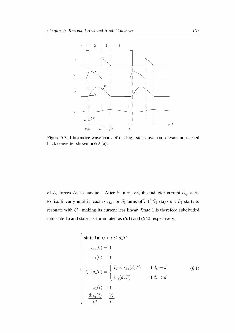
Chapter 6. Resonant Assisted Buck Converter 107
vA
iL1
v1
iL2
t
0 dT TαΤ βΤ
1 2 3 4
V1
V2
I 1
daT
Figure 6.3: Illustrative waveforms of the high-step-down-ratio resonant assistedbuck converter shown in 6.2 (a).
of L2 forces D2 to conduct. After S1 turns on, the inductor current iL1 starts
to rise linearly until it reaches iL2 , or S1 turns off. If S1 stays on, L1 starts to
resonate with C1, making its current less linear. State 1 is therefore subdivided
into state 1a and state 1b, formulated as (6.1) and (6.2) respectively.
state 1a: 0 < t ≤ daT
iL1(0) = 0
v1(0) = 0
iL1(daT ) =
Ia < iL2(daT ) if da = d
iL2(daT ) if da < d
v1(t) = 0
diL1(t)
dt=
VE
L1
(6.1)

108 Chapter 6. Resonant Assisted Buck Converter
state 1b: daT < t ≤ dT
iL1(daT ) = iL2(daT )
v1(daT ) = 0
iL1(dT ) = I1
v1(dT ) = V1
diL1(t)
dt=
VE − v1(t)
L1
dv1(t)
dt=
iL1(t) − iL2(t)
C1
(6.2)
2) State 2 After S1 turns off, L1 and C1 resonate until iL1 = 0. When
iL1 = 0, diode D1 turns off, preventing iL1 from flowing in reverse direction. The
voltage vA is equal to v1, as indicated in Fig. 6.3. The system of equations of state
2 is formulated as follows.
state 2: dT < t ≤ αT
iL1(dT ) = I1
v1(dT ) = V1
iL1(αT ) = 0
v1(αT ) = V2
diL1(t)
dt=
−v1(t)
L1
dv1(t)
dt=
iL1(t) − iL2(t)
C1
(6.3)
3) State 3 After iL1 = 0, capacitor voltage v1 is continuously discharged by
iL2 until it reaches zero. The voltage v1 is kept at zero because iL2 turns on D2

Chapter 6. Resonant Assisted Buck Converter 109
just after v1 = 0. The system of equations of state 3 is formulated as follows.
state 3: αT < t ≤ βT
iL1(t) = 0
v1(αT ) = V2
v1(βT ) = 0
dv1(t)
dt=
−IL2
C1
(6.4)
4) State 4 The voltage v1 is kept at zero because iL2 turns on D2 just after
v1 = 0. The system of equations of state 4 is formulated as follows.
state 4: βT < t ≤ T
iL1(t) = 0
v1(t) = 0
(6.5)
The inductance L2 is designed to be relatively large for the small current
ripple in driving the LED strings. Due to the small current ripple of iL2 , we may
assume that iL2(t) ≈ iL2(t) = IL2 . IL2 varies slowly relative to the time scale
of the switching frequency. Therefore, it can be assumed constant at the time
scale of T . Solving (6.1) and (6.2), we obtain I1(d) and V1(d) in (6.6) and (6.7)
respectively.
I1(d) =
VEdT
L1
if da ≥ d
IL2 +VE
Zr
sin ωr(d − da)T if da < d
(6.6)
V1(d) =
0 if da ≥ d
VE
[1 − cos ωr(d − da)T
]if da < d
(6.7)

110 Chapter 6. Resonant Assisted Buck Converter
where
da =IL2L1
VET, (6.8)
ωr =
√1
L1C1
, and (6.9)
Zr =
√L1
C1
. (6.10)
For high-voltage-step-down applications, ωr(d − da)T is small. Using the
approximation of limx→0 sin x ≈ x, (6.6) can be simplified to
I1(d) ≈ VEdT
L1
. (6.11)
The input power to the power converter can therefore be calculated as
PIN =1
T
∫ dT
0
VEiL1dt ≈ T
2L1
(dVE)2 (6.12)
Solving (6.3), we obtain the following equations for state 2
iL1(t + dT ) = (I1 − IL2) cos ωrt + IL2 −V1
Zr
sin ωrt, and (6.13)
v1(t + dT ) = V1 cos ωrt + (I1 − IL2)Zr sin ωrt. (6.14)
In (6.13) and (6.14), the dependency of I1 and V1 on d are not indicated for clarity.
Rearranging, we get
iL1(t + dT ) = A cos(ωrt + σ) + IL2 , and (6.15)
v1(t + dT ) = AZr sin(ωrt + σ), (6.16)

Chapter 6. Resonant Assisted Buck Converter 111
where
A =√
(I1 − IL2)2 + (V1/Zr)2, and (6.17)
σ = tan−1 V1/Zr
I1 − IL2
. (6.18)
Putting the right hand side of (6.13) to zero, the boundaries of state 2 are
obtained as
α = d +θ − σ
ωrT, and (6.19)
V2 =√
I1(I1 − 2IL2)Z2r + V 2
1 , (6.20)
where
θ = cos−1 −IL2
A. (6.21)
In order that (6.20) has a solution, the following design constraint can be imposed
I1 − 2IL2 ≥ 0. (6.22)
To reduce the conduction time of D1, α can be made small by using a higher ωr.
Solving (6.4), we have
β =V2C1
IL2T+ α. (6.23)
If V2 = 0, we have β = α, where iL1 and v1 reach zero at the same time.

112 Chapter 6. Resonant Assisted Buck Converter
6.3.2 Converter Design for Line Frequency Operation
The converter is controlled by the duty cycle d for the automatic power
factor correction. The input line voltage can be described as
vin(t) = Vm sin ωlt (6.24)
Thus, the instantaneous input power over a line cycle of angular frequency ωl is
given from (6.12) as
PIN(t) =T
2L1
(dVm)2 sin2 ωlt (6.25)
The output voltage VLED is being held up by the charge storage capacitor C2. We
may therefore assume VLED being constant. From power balance and (6.25), we
have
IL2(t) =POUT
VLED
=PIN
VLED
=T
2L1VLED
(dVm)2 sin2 ωlt
=T
4L1VLED
(dVm)2 (1 − cos 2ωlt) (6.26)
The average of IL2 over a line cycle gives ILED. Hence,
ILED = IL2(t) =IL2,max
2=
T
4L1VLED
(dVm)2 (6.27)
6.3.3 Design Procedures and Implementation of the Con-
verter
Based on the line and switching frequency analysis in Sections 6.3.1 and
6.3.2, the design procedures of the converter are given as follows.

Chapter 6. Resonant Assisted Buck Converter 113
1. Denote ILED as the rated DC current of the LEDs.
2. IL2,max is determined as 2ILED from (6.27).
3. To make sure that L1 operates in DCM, d ≤ VLED
vin,max. The maximum duty
cycle dmax is given as dmax = VLED
Vm,min.
4. L1 is determined using L1 = T4VLEDILED
(dmaxVm,min)2 from (6.27). To en-
sure DCM, L1 should be smaller than this value.
5. C1 is determined from fr ≤ fs, where fr is given by (6.9). So C1 ≥
( T2π
)2 1L1
.
6. The maximum of v1 should occur during state 2 in a switching period. From
(6.16), v1 =√
V 21 + (I1 − IL2)
2Z2r and assuming relatively small V1, we
get
v1,max ≈ (I1 − IL2)Zr (6.28)
where I1 is given in (6.6). v1,max occurs at maximum vin such that IL2
equals 2ILED.
7. L2 can be determined using its allowable peak-to-peak current ripples ∆iL2.
From Fig. 6.2(c), we have
L2diL2
dt=
v1,max sin ωrt − VLED dT < t ≤ αT
V2 − IL2
C1t − VLED αT < t ≤ βT
(6.29)
where α, β and V2 are calculated using (6.19), (6.23) and (6.20) respec-
tively.
Integrating (6.29) gives
L2 =1
∆iL2
[v1,max
ωr
(cos ωrT0 − cos ωr(α − d)T ) − VLED ((α − d)T − T0)
]+
1
∆iL2
(V2T1 −
IL2T21
2C1
− VLEDT1
)(6.30)

114 Chapter 6. Resonant Assisted Buck Converter
where T0 = 1ωr
sin−1 VLED
v1,maxand T1 = V2−VLED
V2(β − α)T .
8. C2 is obtained using its allowable peak-to-peak voltage ripple ∆VC2 from
power balance between the input and the output for half of a line period.
From (6.26) and (6.27), IC2(t) = IL2(t)− ILED. Integrating IC2(t) for half
a line period, we have
C2 =POUT
4πflVLED∆VC2
(6.31)
6.4 Experimental Evaluation
A prototype converter shown in Fig. 6.2 (a) has been constructed for perfor-
mance evaluations. For the rated power output of 19.8 V× 0.7 A = 13.72 W, L1
is chosen as 70 µH using design procedures 1 to 4 described in the last section.
The corresponding maximum duty cycle is 0.105 at 100 Vrms AC line input. The
switching frequency is designed at 56 kHz to reduce the switching loss at part
load [129]. Most PWM IC chips do not provide PWM signals of adequate accu-
racy near a duty cycle of 0.1. To generate the required PWM signals efficiently,
the switching frequency is quartered from a 230 kHz PWM generator using D
flip-flops, effectively generating duty cycle from 0 to 0.25 at 56 kHz. Using the
design procedure 5, C1 should be larger than 115 nF. From (6.28), v1,max = 58.6
V. To have ∆iL2
IL2= 20 %, L2 is detemined as 649 µH using (6.30). Fig. 6.4 gives
the value of L2 varying with C1 at a current ripple level of ∆iL2
IL2= 20 %. With
the same ripple current, larger C1, corresponding with smaller L2, will make D1
conduct more and D2 conduct less as indicated in (6.19) and (6.23) respectively.
In practice, the voltage rating of D2 should be above v1,max, Schottky diodes with
a low forward voltage smaller than 0.5 V can be used. While the voltage rating of
D1 is the maximum amplitude of the input AC voltage, an ordinary silicon diode
for D1 having the forward voltage of about 1 V is used. Fig. 6.5 illustrates the

Chapter 6. Resonant Assisted Buck Converter 115
C1 (nF)
L2 (mH)
115 200 300 800400 500 600 700
0
0.2
0.4
0.6
0.3
0.5
0.7
0.1
Figure 6.4: L2 as a function of C1, giving current ripple level of ∆iL2
IL2= 20 %.
0.6
0.8
1
1.2
1.4
C1 (nF)
115 200 300 800400 500 600 700
D1 and D2
conductOnly D1 conducts
D1 conducts in DCM
Buck Converter
Loss_diode (W
)
Figure 6.5: Power loss in diodes at output current ripple level of ∆iL2
IL2= 20 %.
calculated power loss distributed on diodes at the peak voltage of 141 V of the
AC main. When C1 is smaller than 291 nF, D1 and D2 conduct together. Due to
the lower conduction voltage of the Schottky diode D2, the loss in the diodes is
smaller with smaller C1. Fig. 6.6 gives the experimentally measured efficiency
versus the capacitance of C1 with L2 given by Fig. 6.4. Hence, to improve the
efficiency, large L2 and small C1 are selected. Here, we use C1 of 220 nF and
L2 of 457 µH. C2 is 1500 µF to ensure less than 10 % voltage ripple feeding on

116 Chapter 6. Resonant Assisted Buck Converter
100 200 300 400 500 600 7000.918
0.92
0.922
0.924
0.926
0.928
η
0.93
C1 (nF)
Figure 6.6: Efficiency of converter with different values of C1 at 100 Vrms ACinput with output current ripple level of ∆iL2
IL2= 20 %.
0.98
0.985
0.99
0.995
1
1.005
0 2 4 6 8 10 12 14C2 (mF)
Norm
alized Illuminance Efficacy
0
0.1
0.2
0.3
0.4
0.5
Norm
alized current ripple
Figure 6.7: Normalized illuminance efficacy and corresponding current rippleversus different values of C2.
the LED load. As analyzed in Section 6.2, a 63 V rated Vishay capacitor of C2 is
used. Long-lifetime polyester film or ceramic capacitors can be used for C1. D1
is Fairchild ultra-fast diode MUR860. D2 is IR Schottky diode MBR20100CT.
Fig. 6.8 shows the experimental waveforms of vin, iin, VLED and ILED for
100 V and 240 Vrms AC input, respectively, where iin is the line current observed
in front of a line filter consisting of Lf = 300 µH and Cf = 220 nF. LED load
is two parallel branches of 6 cool white Cree LEDs connected in series. Power

Chapter 6. Resonant Assisted Buck Converter 117
[Ch4]LEDI
[Ch2]LEDV
[Ch3]ini
[Ch1]inv
(a)
[Ch4]LEDI
[Ch2]LEDV
[Ch3]ini
[Ch1]inv
(b)
Figure 6.8: Experimental waveforms of vin, iin, VLED and ILED at two line inputvoltages. (a) 100 Vrms AC input. (b) 240 Vrms AC input.
factor is measured to be 0.996 and 0.988 for the two line voltages respectively.
Note that the voltage ripple is about 10 % of VLED. The current ripple is measured
to be as high as 270 mA for ILED = 700 mA. Fig. 6.7 illustrates the normalized
illuminance efficacy (Lux/W) versus C2, showing very little impact of current
ripples on illuminance efficacy. Fig. 6.9 gives the waveforms of vA, v1, iL1 and

118 Chapter 6. Resonant Assisted Buck Converter
[Ch1]Av
1 [Ch2]v
1 [Ch3]Li
2 [Ch4]Li
(a)
[Ch1]Av
1 [Ch2]v
1 [Ch3]Li
2 [Ch4]Li
(b)
Figure 6.9: Experimental waveforms of vA, v1, iL1 and iL2 at two peaks of inputvoltage. (a) 141 V (peak of 100 Vrms line input). (b) 339 V (peak of 240 Vrmsline input).
iL2 at the peak of 100 and 240 Vrms inputs. The small iL2 switching ripples
guarantee the longer lifetime of the output capacitor C2. The efficiency shown
in Fig. 6.10 is typical for low-current applications where switching loss becomes
relatively high with the higher input voltage.

Chapter 6. Resonant Assisted Buck Converter 119
80 100 120 140 160 180 200 220 240 2600.9
0.905
0.91
0.915
0.92
0.925
0.93
Vin (rms, V)
η
Figure 6.10: Converter efficiency versus line input voltage at rated power.
Fig. 6.11 gives two sets of experimental waveforms of the rectified voltage
vrec after the bridge rectifier, v1, iL2 and ILED when the LEDs are dimmed at 100
V rms AC input using trailing edge control. Fig. 6.11(a) uses C1 = 220 nF and
L2 = 457 µH. Fig. 6.11(b) uses C1 = 470 nF and L2 = 204 µH. The values of
C1 and L2 follow Fig. 6.4. Obviously, Fig. 6.11(b) shows more ringings in L2
just after turning off of vrec by the dimmer. The measured efficiencies are 90.56
% and 89.69 % for Figs. 6.11(a) and (b) respectively, showing better efficiency of
using smaller C1.
6.5 Summary
A high-step-down-ratio high-efficiency transformerless resonant assisted buck
converter for LED lamps is proposed for applications of incandescent lamp retrofits.
The discontinuous-conduction-mode operation of the inductor current allows the
simple duty cycle control to achieve both power factor correction and dimmer
device compatibility. Optimization with a resonant assisted filter eliminates the
switching frequency current ripples to the output charge hold-up capacitor, ex-
tending its lifetime. Thus low-cost high-density electrolytic capacitor can be used
in LEDs lighting applications with lifetimes comparable with those of LEDs. The

120 Chapter 6. Resonant Assisted Buck Converter
[Ch2]recv
1 [Ch1]v
2 [Ch3]Li
[Ch4]LEDi
(a)
[Ch2]recv
1 [Ch1]v
2 [Ch3]Li
[Ch4]LEDi
(b)
Figure 6.11: Converter waveforms v1, iL2 and iLED dimmed by vrec using trailingedge control at the same output ripple current of 20 %. (a) C1 = 220 nF and L2 =457 µH. (b) C1 = 470 nF and L2 = 204 µH.
resonant assisted filter also allows using the low-forward-voltage Schottky diode
to improve the converter efficiency. Theoretical calculation and design proce-
dures have been presented for the converter. Experimental verifications have
shown excellent agreement with theoretical predictions.

Chapter 7
Conclusion
In this concluding chapter, we summarize the findings that have been ac-
complished in this project. Some possible future work and potential areas for
further development are also presented.
7.1 Contributions of the Thesis
LED lamps are praised as green lamps in the light of their green properties,
such as energy saving, mercury free, long durability, UV and IR radiation free.
These merits are attracting more attention to LED lighting applications in the in-
dustry. In this thesis, through the studies of color maintenance and LED ballasts,
comprehensive guidelines are provided for designing appropriate LED systems.
Specifically, the contributions of the thesis are stated as follows.
1. Chapter 3 investigates color control methods and analyzes the nonlinear
effects of junction temperature to color precision. A temperature compen-
sation technique using the LED turn-on voltage during the on-state of a
PWM period has been proposed. The technique can control the color ef-
121

122 Chapter 7. Conclusion
fectively, dramatically reduce the complexity, and eliminate the need for
using expensive feedback systems involving lighting sensors. The system
has been ported to a fully automatic computerized system for industrial
implementation.
2. Chapter 4 proposes a transformer isolated boost PFC pre-regulator oper-
ating in discontinuous conduction mode for LED ballasts in order to sat-
isfy the current harmonic limits and achieve high voltage step-down. The
pre-regulator uses the resonant technique to take advantage of the leakage
inductance commonly found in high voltage step-down transformers. The
resonant circuit allows the output charge storage capacitor to be placed
at the secondary of the transformer. In this way, the short-lifetime high-
voltage charge storage capacitor is no longer required. Instead, a low-
voltage long-lifetime capacitor can be used to extend the overall system
lifetime. The resonance structure also takes full advantage of the leakage
inductance of the high turns-ratio transformer to alleviate the voltage and
current stresses, improving the lifetime of main switching components.
3. Chapter 5 derives the conditions for the converter in Chapter 4 to be op-
erated in continuous conduction mode for high power applications. This
chapter also presents a non-cascading configuration at the secondary of the
PFC pre-regulator to improve the overall efficiency via two output wind-
ings of the transformer. One of the outputs is connected directly (without
being processed) in series with the other output which is then current reg-
ulated by a PWM buck converter to drive an LED lamp. Since the energy
from one output winding can directly be used to drive the LED without
going through another power stage, a higher efficiency can be guaranteed.
A detailed design and optimization procedures are given and the results are
verified by experiments.
4. Finally, in applications with power lower than 25 W, the current harmonic
requirements are less stringent as stated in some international standards. A

Chapter 7. Conclusion 123
high-step-down-ratio and high-efficiency resonant assisted buck converter
for LED lamps is proposed in Chapter 6 for the application of incandescent
replacement lamps. The transformerless design boosts the converter effi-
ciency. The discontinuous conduction mode operation allows simple duty
cycle control and is compatible with dimmer devices.
7.2 Suggestions for Future Work
The unique features of LEDs arouse great concern and interest of academia
and industry in lighting applications. Based on the previous work and experience
gathered in the recent decade, and the work done in this project, suggestions for
extensions and potential areas for further studies are proposed here.
PWM of the LED driving current and measurement of the LED diode for-
ward voltage have been used for light color maintenance in Chapter 3. Investi-
gation of other current modulation methods is an interesting topic to study. The
use of PWM current driving provides predictable relationship between duty cycle
and light intensity with minimum alteration of other light properties. However,
the PWM dimming technique may have poor efficacy when the LED is driven
at some high current levels where the optical light output becomes saturated. In
such applications where the LEDs are driven near saturation for optimization of
the total achievable output lumen, dimming by AM will be a better alternative to
achieve a higher luminous efficacy. However, it is predicted that the AM dim-
ming for color maintenance can be complicated. The kinds of relationships that
exist among the electrical-thermal-optical behavior remain unknown. With the
boost in digital-signal-processor (DSP) programming powers, the compensation
may be achievable even if complex computations are involved.
For a LED having 75 lm/W, about 90 % of its electrical energy will be con-
verted to heat. Almost 90 % of the heat generated is not radiative and needs to be

124 Chapter 7. Conclusion
removed conductively. Thermal management of the LED light source becomes
an important issue for LED lighting applications in order to keep the LED below
its operating temperature. Otherwise its light output may be reduced and chip
degradation accelerated. Thermal management components such as heat sinks,
piezo fans, thermoelectric coolers, metal core PCBs and heat pipes are actively
researched for LED applications. Optimization of these thermal management
components specifically for LED applications can improve light output and pro-
long LED lifetime.
In the research of LED ballasts, we have proposed several driving circuits
for different power-level applications, targeting at improving lifetime and effi-
ciency. Other areas such as integrated magnetics and soft switching can be inves-
tigated to improve the power density and cost of LED ballasts.
For ease of thermal management, a single LED can provide about 100 lm
light output. In many applications, such as those used in stadiums, high lumen
flux of more than 1000 lm per lamp is needed. Several LED lamps are connected
in series or parallel to provide enough brightness driven by a single ballast for
cost saving. LED binning is used to overcome device variation in electrical and
optical properties, but this increases the cost. Therefore, circuits for automatic
current sharing or voltage sharing can be an important topic for investigation.

Bibliography
[1] BL-4000 Series datasheet, “RGB + LED light engine,” Lamina Lighting
Inc., 2005.
[2] Atlas Series datasheet, “Atlas LED light engines datasheet,” Lamina
Lighting Inc., 2006.
[3] X42180 datasheet, “X42180 technical data sheet,” Seoul Semiconductor
Inc., 2009.
[4] Philips Technology white paper, “Understanding power LED lifetime
analysis,” Philips Lumileds Lighting Int., 2007.
[5] R. Friedel and P. Israel, Edison′s Electric Light: Biography of an Invention.
New Jersey, NJ: Rutgers University Press, 1986.
[6] T. Hughes, American Genesis: A Century of Invention and Technological
Enthusiasm. Chicago, IL: The University of Chicago Press, 1990.
[7] L. J. Davis, Fleet Fire: Thomas Edison and the Pioneers of the Electric
Revolution. New York, NY: Arcade Publishing, 2003.
[8] J. Waymouth, Electric Discharge Lamps. Cambridge, MA: The MIT
Press, 1971.
[9] D. O. Wharmby, “Electrodeless lamps for lighting: a review,” Proceedings
of IEE Science, Measurement and Technology, vol. 140, pp. 465–473, Nov.
1993.
125

126 BIBLIOGRAPHY
[10] W. Elenbaas, Fluorescent Lamps. London, U.K.: Macmillan, 1971.
[11] J. A. Sigler, J. F. Crutchfield, and H. C. Wilins, The Fluorescent Lamp.
New York, NY: McGraw-hill Book Company, 1975.
[12] K. H. Butler, Fluorescent Lamp Phosphors: Technology and Theory. New
Jersey, NJ: Pennsylvania State University Press, 1980.
[13] W. Elenbaas, The High Pressure Mercury Vapor Discharge. London,
U.K.: Interscience Publishers, 1951.
[14] ——, High-Pressure Mercury Vapor Lamps and Their Applications.
Eindhoven, Netherlands: Philips Technical Library, 1965.
[15] P. Flesch, Light and Light Sources: High-Intensity Discharge Lamps.
Berlin, Germany: Springer, 2006.
[16] A. Zukauskas, M. S. Shur, and R. Gaska, Introduction to Solid-State Light-
ing. New York, NY: Wiley, 2002.
[17] E. F. Schubert, Light-Emitting Diodes. London, U.K.: Cambridge Uni-
versity Press; 2nd edition, 2006.
[18] M. S. Shur and A. Zukauskas, UV Solid-State Light Emitters and Detec-
tors. Netherlands: Kluwer, 2004.
[19] F. Richard, Light-emitting Diodes: A Guide to the Technology and its Ap-
plications. Bracknell, UK: BSRIA, 2005.
[20] G. Held, Introduction to Light Emitting Diode Technology and Applica-
tions. London, U.K.: Taylor and Francis; 1st edition, 2008.
[21] P. Mottier, LED for Lighting Applications. New York, NY: Wiley-ISTE,
2009.
[22] Department of Energy, U.S. [Online]. Available: http://www.energy.gov/

BIBLIOGRAPHY 127
[23] C. DiLouie, Advanced Lighting Controls: Energy Savings, Productivity,
Technology and Applications. Lilburn, GA: The Fairmont Press; 1st edi-
tion, 2005.
[24] D. Derbyshire, “Revolt! robbed of their right to buy traditional light bulbs,
millions are clearing shelves of last supplies,” The Daily Mail, 2009.
[25] (2008) Grosses lichterloschen fur die gluhbirnen. [On-
line]. Available: http://www.tagesanzeiger.ch/leben/rat-und-tipps/
Grosses-Lichterlschen-fr-die-Glhbirnen/story/25999013
[26] (2009) Desde 2011, no podran venderse mas lamparas incandescentes.
[Online]. Available: http://www.lanacion.com.ar/nota.asp?nota$ $id=
1091978
[27] L. Cockcroft, “Traditional light bulbs to be phased out in favour of low-
energy alternative,” The Daily Telegraph, 2009.
[28] B. Tenille, “Critics blast environment plan as out of sync with science,”
The Globe and Mail, 2007.
[29] (2007) Oida market forecast for solid stage lighting. [Online]. Available:
http://wrtassoc.com/
[30] S. Nakamura and G. Fasol, The Blue Laser Diode: GaN Based Light Emit-
ters and Lasers. Berlin, Germany: Springer-Verlag, 1997.
[31] S. Nakamura and S. F. Chichibu, Introduction to Nitride Semiconductor
Blue Lasers and Light Emitting Diodes. London, U.K.: Taylor and Fran-
cis, 2000.
[32] J. Kalinowski, Organic Light-Emitting Diodes: Principles, Characteris-
tics and Processes, New York, NY, 2004.

128 BIBLIOGRAPHY
[33] J. Edmond, A. Abare, M. Bergman, J. Bharathan, and et al., “High effi-
ciency GaN-based LEDs and lasers on SiC,” Journal of Crystal Growth,
vol. 272, pp. 242–250, Nov. 2004.
[34] B. Johnstone, Brilliant!: Shuji Nakamura and the Revolution in Lighting
Technology. New York, NY: Prometheus Books, 2007.
[35] N. Holonyak, Jr., “Is the light emitting diode (LED) an ultimate lamp?,”
American Journal of Physics, vol. 68, no. 9, pp. 864–866, Sep. 2000.
[36] J. Tsao, “Solid-state lighting: lamps, chips and materials for tomorrow,”
in Proceedings of Conference on Lasers and Electro-Optics (CLEO), May
2005, pp. 143–143.
[37] Y. Narukawa, J. Narita, T. Sakamoto, K. Deguchi, T. Yamada, and
T. Mukai, “Ultra-high efficiency white light-emitting diodes,” Japanese
Journal of Applied Physics, vol. 45, pp. L1084–L1086, Oct. 2006.
[38] M. R. Krames, O. B. Shchekin, R. Mueller-Mach, G. O. Mueller, L. Zhou,
G. Harbers, and M. G. Craford, “Status and future of high-power light-
emitting diodes for solid-state lighting,” IEEE/OSA Journal of Display
Technology, vol. 3, no. 2, pp. 160–175, Jun. 2007.
[39] (2009) Renewables global states report 2009 update. [Online]. Available:
http://www.ren21.net/pdf/RE$ $GSR$ $2009$ $Update.pdf
[40] M. S. Shur and A. Zukauskas, “Solid-state lighting: toward superior il-
lumination,” Proceedings of IEEE, vol. 93, no. 10, pp. 1691–1703, Oct.
2005.
[41] C. C. Chen, C. Y. Wu, and T. F. Wu, “LED back-light driving system for
LCD panels,” in Proceedings of IEEE Applied Power Electronics Confer-
ence and Exposition (APEC), Mar. 2006, pp. 381–385.

BIBLIOGRAPHY 129
[42] C. C. Chen, C. Y. Wu, Y. M. Chen, and T. F. Wu, “Sequential color LED
backlight driving system for LCD panels,” IEEE Transactions on Power
Electronics, vol. 22, no. 3, pp. 919–925, May 2007.
[43] H. J. Chiu, Y. K. Lo, T. P. Lee, S. C. Mou, and H. M. Huang, “Design
of an RGB LED backlight circuit for liquid crystal display panels,” IEEE
Transactions on Industrial Electronics, vol. 58, no. 7, pp. 2793–2795, Jul.
2009.
[44] K. Saucke, G. Pausch, J. Stein, H. G. Ortlepp, and P. Schotanus, “Stabiliz-
ing scintillation detector systems with pulsed LEDs: a method to derive
the led temperature from pulse height spectra,” IEEE Transactions on Nu-
clear Science, vol. 52, no. 6, pp. 3160–3165, Dec. 2005.
[45] A. E. Moe, N. Banani, L. A. Lee, B. Marquardt, and D. M. Wilson,
“Enhanced fluorescence emission using a programmable, reconfigurable
LED-array based light source,” vol. 3, Sep. 2004, pp. 2090–2093.
[46] D. A. Steigerwald, J. C. Bhat, D. Collins, R. M. Fletcher, M. O. Holcomb,
and M. J. Ludowise, “Illumination with solid state lighting technology,”
IEEE Journal of Selected Topics in Quantum Electronics, vol. 8, no. 2, pp.
310–320, Mar./Apr. 2002.
[47] E. F. Schubert and H. W. Yao, Light-emitting diodes: research, manufac-
turing and applications. SPIE-Int. Society for Optical Engine, 2006.
[48] S. Muthu, F. J. Schuurmans, and M. D. Pashley, “Red, green, and blue
LEDs for white light illumination,” IEEE Journal of Selected Topics in
Quantum Electronics, vol. 8, no. 2, pp. 333–338, Mar./Apr. 2002.
[49] ——, “Red, green, and blue LED based white light generation: issues and
control,” in Proceedings of IEEE Industry Application Society Conference
(IAS), Oct. 2002, pp. 327–333.

130 BIBLIOGRAPHY
[50] S. Muthu and J. Gaines, “Red, green, and blue LED based white light gen-
eration: implementation challenges and control design,” in Proceedings of
IEEE Industry Application Society Conference (IAS), Oct. 2003, pp. 515–
522.
[51] B. Ackermann, V. Schulz, C. Martiny, A. Hilgers, and X. Zhu, “Control of
LEDs,” in Proceedings of IEEE Industry Application Society Conference
(IAS), Oct. 2006, pp. 2608–2615.
[52] M. Dyble, N. Narendran, A. Bierman, and T. Klein, “Impacts of dimming
white LEDs: Chromaticity shifts due to different dimming methods,” Pro-
ceedings of International Society for Optical Engineering (SPIE), pp. 280–
288, Jul./Aug. 2005.
[53] G. Farkas, A. Poppe, J. Schanda, and K. Muray. (2004) Complex
characterization of power LEDs: simultaneous measurement of
photometric/radiometric and thermal properties. [Online]. Available:
http://www.knt.vein.hu/staff/schandaj/SJCV-Publ-2005/503.pdf
[54] N. Narendran and Y. Gu, “Life of LED-based white light sources,”
IEEE/OSA Journal of Display Technology, vol. 1, no. 1, pp. 167–171, Sep.
2005.
[55] S. Winder, Power Supplies for LED Driving. Burlington, MA: Newnes,
2008.
[56] L. R. Nerone, “Design of a 2.5-Mhz, soft-switching, class-D converter for
electrodeless lighting,” IEEE Transactions on Power Electronics, vol. 12,
no. 3, pp. 507–516, May 1997.
[57] B. Y. Shmuel, M. Shvartsas, and S. Glozman, “Statics and dynamics of
fluorescent lamps operating at high frequency: modeling and simulation,”
IEEE Transactions on Industry Applications, vol. 38, no. 6, pp. 1486–
1492, Nov/Dec. 2002.

BIBLIOGRAPHY 131
[58] T. E. Jang, H. J. Kim, and H. Kim, “Dimming control characteristics of
electrodeless fluorescent lamps,” IEEE Transactions on Industrial Elec-
tronics, vol. 56, no. 1, pp. 93–100, Jan. 2009.
[59] J. H. Campbell, “Initial characteristics of high intensity discharge lamps
on high frequency power,” Journal of Illumimating Engineering Society,
vol. 64, no. 12, pp. 713–722, Dec. 1969.
[60] R. Fiorello, “Powering a 35W DC metal halide HID lamp using the
UCC3305 HID lamp controller,” Unitrode Application Note U-161, 1999.
[61] ——, “Low-cost high power-density electronic ballast for automotive HID
lamp,” IEEE Transactions on Power Electronics, vol. 15, no. 2, pp. 361–
368, Mar. 2000.
[62] W. S. Kim, B. H. Cho, and K. C. Lee, “Design and analysis of high-voltage
transformer for HID lamp igniter,” in Proceedings of IEEE Applied Power
Electronics Conference and Exposition (APEC), vol. 2, Mar. 2005, pp.
1043–1047.
[63] H. J. Chiu, T. H. Song, S. J. Cheng, C. H. Li, and Y. K. Lo, “Design
and implementation of a single-stage high-frequency HID lamp electronic
ballast,” IEEE Transactions on Industrial Electronics, vol. 55, no. 2, pp.
674–683, Feb. 2008.
[64] G. Sauerlander, D. Hente, H. Radermacher, E. Waffenschmidt, and J. Ja-
cobs, “Driver electronics for LEDs,” in Proceedings of IEEE Industry Ap-
plication Society Conference (IAS), vol. 5, Oct. 2006, pp. 2621–2626.
[65] R. Mueller-Mach, G. O. Mueller, M. R. Krames, and T. Trottier, “High-
power phosphor-converted light-emitting diodes based on III-nitrides,”
IEEE Journal of Selected Topics in Quantum Electronics, vol. 8, no. 2,
pp. 339–345, Mar./Apr. 2002.

132 BIBLIOGRAPHY
[66] G. Wyszecki and W. S. Stiles, Color Science. New York, NY: Wiley,
1982.
[67] D. L. MacAdam, Color Measurements: Theme and Variations. New
York, NY: Springer-Verlag, 1985.
[68] S. Nakamura, T. Mukai, and M. Senoh, “Candela-class high-brightness
GaInN/AlGaN double-heterostructure blue-light-emitting diodes,” Ap-
plied Physics Letters, vol. 64, no. 13, pp. 1687–1689, Mar. 1994.
[69] G. B. Stringfellow and M. G. Craford, High Brightness Light Emitting
Diodes. San Diego, CA: Academic Press, 1997.
[70] T. Tamura, T. Setomoto, and T. Taguchi, “Illumination characteristics of
lighting array using 10 candela-class white LED under AC 100V opera-
tion,” Journal of Luminescence, vol. 87-89, pp. 1180–1182, Apr. 2000.
[71] E. Hong, “A non-contact method to determine junction temperature of
hihg-brightness(AlGaInP) light emitting diodes,” Master thesis, Rensse-
laer Polytechnic Institute, Troy, NY, 2003.
[72] W. S. Oh, D. Cho, K. M. Cho, G. W. Moon, B. Yang, and T. Jang, “A novel
two-dimensional adaptive dimming technique of X-Y channel drivers for
LED backlight system in LCD TVs,” IEEE/OSA Journal of Display Tech-
nology, vol. 5, no. 1, pp. 20–26, Jan. 2009.
[73] X. Xu and X. Wu, “High dimming ratio LED driver with fast transient
boost converter,” in Record of IEEE Power Electronics Specialists Confer-
ence (PESC), Jun. 2008, pp. 4192–4195.
[74] H. M. Huang, S. H. Twu, S. J. Cheng, and H. J. Chiu, “A single-stage
SEPIC PFC converter for multiple lighting LED lamps,” in Proceedings
of IEEE International Sympomium on Electronic Design, Test and Appli-
cation, Jan. 2008, pp. 15–19.

BIBLIOGRAPHY 133
[75] M. Doshi and R. Zane, “Reconfigurable and fault tolerant digital phase
shifted modulator for luminance control of LED light sources,” in Record
of IEEE Power Electronics Specialists Conference (PESC), Jun. 2008, pp.
4185–4191.
[76] Y. Gu and N. Narendran, “A non-contact method for determining junction
temperature of phosphor-converted white LEDs,” in Proceedings of Inter-
national Society for Optical Engineering (SPIE), vol. 5187, Jan. 2004, pp.
107–114.
[77] N. Narendran, Y. Gu, and R. Hosseinzadeh, “Estimating junction tempera-
ture of high-flux white LEDs,” in Proceedings of International Society for
Optical Engineering (SPIE), vol. 5366, Jan. 2004, pp. 158–160.
[78] P. Pinho, E. Tetri, and L. Halonen, “Synergies of controller-based LED
drivers and quality solid-stage lighting,” in Proceeding of IEEE Research
in Microelectronics and Electronics, Jun. 2006, pp. 405–408.
[79] E. Mineiro Sa Jr., F. L. M. Antunes, and A. J. Perin, “Junction temperature
estimation for high power light-emitting diodes,” in Proceedings of IEEE
International Symposium on Industrial Electronics (ISIE), Jun. 2007, pp.
3030–3035.
[80] A. Perduijn, S. de Krijger, J. Claessens, and et al. (2003) Light output feed-
back solution for RGB LED backlight applications. [Online]. Available:
http://www.philipslumileds.com/pdfs/LOPFeedback4backlight.PDF
[81] A. Zukauskas, R. Vaicekauskas, and F. I. et al, “Quadrichromatic white
solid state lamp with digital feedback,” in Proceedings of International
Society for Optical Engineering (SPIE), vol. 5187, Jan. 2004, pp. 185–
198.

134 BIBLIOGRAPHY
[82] I. E. Ashdown, “Neural networks for LED color control,” in Proceedings
of International Society for Optical Engineering (SPIE), vol. 5187, Jan.
2004, pp. 215–226.
[83] P. Deurenberg, C. Hoelen, J. van Meurs, and J. Ansems, “Achieving color
point stability in RGB multi-chip LED modules using various color con-
trol loops,” in Proceedings of International Society for Optical Engineer-
ing (SPIE), vol. 5941, Jul./Aug. 2005, pp. 63–74.
[84] K. Lim, J. C. Lee, G. Panotopoulos, and R. Helbing, “Illumination and
color management in solid state lighting,” in Proceedings of IEEE Industry
Application Society Conference (IAS), Oct. 2006, pp. 2616–2620.
[85] J. Garcia, M. A. Dalla-Costa, J. Cardesin, J. M. Alonso, and M. Rico-
Secades, “Dimming of high-brightness LEDs by means of luminous flux
thermal estimation,” IEEE Transactions on Power Electronics, vol. 30,
no. 2, pp. 1107–1114, Apr. 2009.
[86] EN 61000-3-2, “Electromagnetic compatibility (EMC) – Part 3-2: Limits–
limits for harmonic current emissions (equipment input current ≤ 16 A per
phase),” 2006.
[87] M. Rico-Secades, A. J. Calleja, J. Ribas, E. L. Corominas, J. M. Alonso,
and J. Garcia, “Driver for high efficiency LED based on flyback stage
with current mode control for emergency lighting system,” in Proceedings
of IEEE Industry Application Society Conference (IAS), Oct. 2004, pp.
1655–1659.
[88] G. Spiazzi, S. Buso, and G. Meneghesso, “Analysis of a high-power-factor
electronic ballast for high brightness light emitting diodes,” in Record of
IEEE Power Electronics Specialists Conference (PESC), Jun. 2005, pp.
1494–1499.

BIBLIOGRAPHY 135
[89] M. Rico-Secades, A. J. Calleja, J. Ribas, E. L. Corominas, J. M. Alonso,
J. Cardesin, and J. Carcia-Garcia, “Evaluation of a low-cost permanent
emergency lighting system based on high-efficiency LEDs,” IEEE Trans-
actions on Industry Applications, vol. 41, no. 5, pp. 1386–1390, Sep./Oct.
2005.
[90] H.-J. Chiu and S.-J. Cheng, “LED backlight driving system for large-scale
LCD panels,” IEEE Transactions on Power Electronics, vol. 54, no. 5, pp.
2751–2760, Oct. 2007.
[91] G. Carraro, “Solving high-voltage off-line HB-LED constant current
control-circuit issues,” in Proceedings of IEEE Applied Power Electron-
ics Conference and Exposition (APEC), Feb. 2007, pp. 1316–1318.
[92] J. Sebastian, D. G. Lamar, M. Arias, M. Rodriguez, and M. M. Hernando,
“A very simple control strategy for power factor correctors driving high-
brightness light-emitting diodes,” in Proceedings of IEEE Applied Power
Electronics Conference and Exposition (APEC), Feb. 2008, pp. 537–543.
[93] Y. Hu and M. M. Jovanovic, “LED driver with self-adaptive drive voltage,”
IEEE Transactions on Power Electronics, vol. 23, no. 6, pp. 3116–3125,
Nov. 2008.
[94] Z. Ye, F. Greenfield, and Z. Liang, “A topology study of single-phase
offline AC/DC converters for high brightness white LED lighting with
power factor pre-regulation and brightness dimmable,” in Proceedings of
IEEE Conference on Industrial Electronics, Control and Instrumentations
(IECON), Nov. 2008, pp. 1961–1967.
[95] ——, “Offline SEPIC converter to drive the high brightness white LED
for lighting applications,” in Proceedings of IEEE Conference on Indus-
trial Electronics, Control and Instrumentations (IECON), Nov. 2008, pp.
1994–2000.

136 BIBLIOGRAPHY
[96] S. K. Maddula and J. C. Balda, “Lifetime of electrolytic capacitors in re-
generative induction motor drives,” in Record of IEEE Power Electronics
Specialists Conference (PESC), Jun. 2005, pp. 153–159.
[97] H. van der Broeckl, G. Sauerlander, and M. Wendt, “Power driver topolo-
gies and control schemes for LEDs,” in Proceedings of IEEE Applied
Power Electronics Conference and Exposition (APEC), Feb. 2007, pp.
1319–1325.
[98] Y. Qin, S. H. Chung, D. Y. Lin, and S. Y. R. Hui, “Current source ballast
for high power lighting emitting diodes without electrolytic capacitor,” in
Proceedings of IEEE Conference on Industrial Electronics, Control and
Instrumentations (IECON), Nov. 2008, pp. 1968–1973.
[99] L. Gu, X. Ruan, M. Xu, and K. Yao, “Means of eliminating electrolytic ca-
pacitor in AC/DC power supplies for LED lightings,” IEEE Transactions
on Power Electronics, vol. 24, no. 5, pp. 1399–1408, May 2009.
[100] H. Chung, S. Y. R. Hui, and W. H. Wang, “An isolated ZVS/ZCS flyback
converter using the leakage inductance of the coupled inductor,” IEEE
Transactions on Industrial Electronics, vol. 45, no. 4, pp. 679–682, Aug.
1998.
[101] K. Gillessen and W. Schairer, Light Emitting Diodes: An Introduction.
New Jersey, NJ: Prentice Hall, 1987.
[102] Department of Energy, U.S., “ENERGY STAR program requirements for
solid state lighting luminaires,” Dec. 2008.
[103] International Electrotechnical Commission (IEC). [Online]. Available:
http://www.iec.ch/
[104] EN 60598-1, “luminaires – Part1: General requirements and tests,” 2008.
[105] EN 62031, “LED modules for general lighting – safety specifications,”
2008.

BIBLIOGRAPHY 137
[106] EN 61347-2-13, “Lamp controlgear – Part 2-13: Particular requirements
for d.c. or a.c. supplied electronic controlgear for LED modules,” 2006.
[107] EN 55015, “Limits and methods of measurement of radio disturbance char-
acteristics of electrical lighting and similar equipment,” 2009.
[108] A. I. Pressman, Switching power supply design. New York, NY: McGraw
Hill, 1998.
[109] R. W. Erickson and D. Maksimovic, Fundamentals of power electronics.
Norwell, MA: Kluwer Academic Publishers, 2001.
[110] G. D. Youle, “Light source control system,” U.S. Patent 7 067 993, Jun.,
2006.
[111] L. De Oto and T. E. Clary, “LED brightness compensation system and
methods,” European Patent EP1 901 587A2, Mar., 2008.
[112] Linear Technology. (1995) Constant-voltage / constant-current bat-
tery charger. [Online]. Available: http://www.datasheetcatalog.com/
datasheets pdf/L/T/1/5/LT1510.shtml
[113] V. Misra, W. Gong, and D. Towsley, “Fluid-based analysis of a network
of AQM routers supporting TCP flows with application to RED,” ACM
SIGCOMM Computer Communication Review, vol. 30, no. 4, pp. 151–
160, Oct. 2000.
[114] Oceanoptic Inc. (2008, Nov.) LED brightness compensation system and
methods. [Online]. Available: http://www.oceanoptics.com/
[115] O. Garcia, J. A. Cobos, R. Prieto, P. Alou, and J. Cueda, “Single phase
power factor correction: a survey,” IEEE Transactions on Power Electron-
ics, vol. 18, no. 3, pp. 749–755, May 2003.

138 BIBLIOGRAPHY
[116] H. Wei, I. Batarseh, G. Zhu, and P. Kornetzky, “A single-switch AC-
DC converter with power factor correction,” IEEE Transactions on Power
Electronics, vol. 15, no. 3, pp. 421–430, May 2000.
[117] Q. Zhao, M. Xu, F. C. Lee, and J. Qian, “Single-switch parallel power
factor correction AC-DC converters with inherent load current feedback,”
IEEE Transactions on Power Electronics, vol. 19, no. 4, pp. 928–936, Jul.
2004.
[118] T. F. Wu, J. C. Hung, S. Y. Tseng, and Y. M. Chen, “A single-stage fast
regulator with PFC based on an asymmetrical half-bridge topology,” IEEE
Transactions on Industrial Electronics, vol. 52, no. 1, pp. 139–150, Feb.
2005.
[119] D. Fu, F. C. Lee, Q. Yang, and F. Wang, “A novel high-power-density
three-level LLC resonant converters with constant-power-factor-control
for charging appilcations,” IEEE Transactions on Power Electronics,
vol. 23, no. 5, pp. 2411–2420, Sep. 2008.
[120] C. K. Tse, “Circuit theory of power factor correction in switching convert-
ers,” International Journal of Circuit Theory and Applications, vol. 31,
no. 2, pp. 157–198, Feb. 2003.
[121] S. Luo, W. Qiu, W. Wu, and I. Batarseh, “Flyboost power factor correction
cell and a new family of single-stage AC/DC converters,” IEEE Transac-
tions on Power Electronics, vol. 20, no. 1, pp. 25–34, Jan. 2005.
[122] A. Lazaro, A. Barrado, M. Sanz, V. Salas, and E. Olıas, “New power fac-
tor correction AC-DC converter with reduced storage capacitor voltage,”
IEEE Transactions on Industrial Electronics, vol. 54, no. 1, pp. 384–397,
Feb. 2007.
[123] M. K. H. Cheung, M. H. L. Chow, and C. K. Tse, “Practical design and
evaluation of a 1 kW PFC power supply based on reduced redundant

BIBLIOGRAPHY 139
power processing principle,” IEEE Transactions on Industrial Electronics,
vol. 55, no. 2, pp. 665–673, Feb. 2008.
[124] Vishay BC components. (2008) Aluminum capacitors power standard
miniature snap-in 056/057 psm-si. [Online]. Available: http://www.
farnell.com/datasheets/415179.pdf
[125] D. D. C. Lu, H. H. C. Iu, and V. Pjevalica, “A single-stage AC/DC con-
verter with high power factor, regulated bus voltage, and output voltage,”
IEEE Transactions on Power Electronics, vol. 23, no. 1, pp. 218–228, Jan.
2008.
[126] P. C. Todd, “UC3854 controlled power factor correction circuit design,”
Unitrode application note U-134, 1997.
[127] D. Fu, F. C. Lee, and M. Xu, “A novel driving scheme for synchronous
rectifiers in LLC resonant converters,” IEEE Transactions on Power Elec-
tronics, vol. 24, no. 5, pp. 1321–1329, May 2009.
[128] XR-E Series datasheet, “Cree Xlamp XR-E LED data sheet,” Cree Inc.,
2009.
[129] J. Sun, M. Xu, Y. Ren, and F. C. Lee, “Light-load efficiency improve-
ment for buck voltage regulators,” IEEE Transactions on Power Electron-
ics, vol. 24, no. 3, pp. 742–751, Mar. 2009.