design of measurement circuits for sic...
TRANSCRIPT
DEGREE PROJECT IN ELECTRONICS AND COMPUTER ENGINEERING,FIRST CYCLE, 15 CREDITSSTOCKHOLM, SWEDEN 2016
Design of measurement circuits for SiC experimentKTH student satellite MIST
MATTHIAS ERICSON
JOHAN SILVERUDD
KTH ROYAL INSTITUTE OF TECHNOLOGYSCHOOL OF INFORMATION AND COMMUNICATION TECHNOLOGY


Abstract
SiC in Space is one of the experiments on KTH’s miniature satellite, MIST. The experiment carries out tests on bipolar junction transistors of silicon and silicon carbide. This thesis describes how the characteristics of a transistor can be measured using analog circuits. The presented circuit design will work as a prototype for the SiC in Space experiment. The prototype measures the base current, the collector current, the base-emitter voltage as well as the temperature of the transistor. This thesis describes how a test circuit may be designed. The selected design has been constructed in incremental steps, with each design choice explained. Different designs have been developed. The designs have been verified with simulations. We have also constructed and tested three different prototypes on breadboards and printed circuit boards. Keywords: MIST, CubeSat, Silicon carbide, Amplifiers, PCB design, Analog electronics, Bipolar Junction Transistors, Measurement circuit.


Abstract
SiC in Space är ett av experimenten på KTHs miniatyrsatellit, MIST. Experimentet utför test på bipolära transistorer av kisel och kiselkarbid. Detta examensarbete förklarar hur transistorns karakteristik kan mätas med analoga kretsar. Den framtagna kretsdesignen kommer att fungera som en prototyp till SiC in Space-experimentet. Prototypen mäter basströmmen, kollektorströmmen, bas-emitter-spänningen samt temperaturen för transistorn. Detta examensarbete förklarar hur en testkrets kan designas. Den valda designen byggs i inkrementella steg, där varje designval förklaras. Olika designer har utvecklats. Designerna har verifierats genom simuleringar. Vi har också konstruerat och testat tre olika prototyper på kopplingsdäck och kretskort. Nyckelord: MIST, CubeSat, Kiselkarbid, Förstärkare, Kretskortsdesign, Analog elektronik, Bipolära transistorer, Mätkrets.


Acknowledgment We would like to thank our supervisor Bengt Molin and examiner professor Carl-Mikael Zetterling for the support they have provided during this project. We also would like to thank our fellow team members for their collaboration in the SiC in Space project; Mikael André, Simon Johansson, and Hannes Paulsson. Stockholm, June 2016 Matthias Ericson and Johan Silverudd


1
Table of Contents
List of figures ........................................................................................................................ 3
List of tables .......................................................................................................................... 4
List of abbreviations .......................................................................................................... 5
1 Introduction ................................................................................................................. 7 1.1 Background ..................................................................................................................... 7 1.2 Problem............................................................................................................................. 7 1.3 Purpose ............................................................................................................................. 8 1.4 Goal ..................................................................................................................................... 8 1.5 Benefits, Ethics, and Sustainability ......................................................................... 8 1.6 Delimitations .................................................................................................................. 8 1.7 Outline ............................................................................................................................... 9
2 Method ........................................................................................................................ 10 2.1 Duration and location ................................................................................................ 10 2.2 Organization .................................................................................................................. 10 2.3 Literature ....................................................................................................................... 10 2.4 Circuit design ................................................................................................................ 10 2.5 Software .......................................................................................................................... 10 2.6 Testing ............................................................................................................................. 11
3 Theory ......................................................................................................................... 12 3.1 Bipolar Junction Transistor ..................................................................................... 12 3.2 Operational Amplifier ................................................................................................ 13
3.2.1 Non-inverting amplifier .....................................................................................................15 3.2.2 Inverting amplifier ...............................................................................................................16 3.2.3 Buffer .........................................................................................................................................17 3.2.4 Differential amplifier ..........................................................................................................18 3.2.5 Instrumental amplifier .......................................................................................................20
3.3 Temperature ................................................................................................................. 21
4 System architecture ............................................................................................... 24 4.1 DC/DC converter .......................................................................................................... 24 4.2 Test circuitry ................................................................................................................. 24 4.3 Microcontroller ............................................................................................................ 25
5 Test circuits ............................................................................................................... 26 5.1 Supply voltage .............................................................................................................. 26
5.1.1 Power matrix ..........................................................................................................................26 5.1.2 Linear DC/DC converter from battery power ..........................................................26 5.1.3 Decoupling capacitors ........................................................................................................26
5.2 Adjustable settings...................................................................................................... 27 5.2.1 Switches ...................................................................................................................................27 5.2.2 Current generator ................................................................................................................30 5.2.3 Using a DAC .............................................................................................................................31 5.2.4 Using a DAC with operational amplifier......................................................................31 5.2.5 Constant collector-emitter voltage ...............................................................................31
5.3 Measurement ................................................................................................................ 33
2
5.3.1 Voltage divider ......................................................................................................................33 5.3.2 Buffer .........................................................................................................................................34 5.3.3 Instrumental amplifier .......................................................................................................34 5.3.4 Temperature measurement .............................................................................................35 5.3.5 Over voltage protection .....................................................................................................36 5.3.6 Measuring using pulsed mode ........................................................................................37
5.4 EMC ................................................................................................................................... 37 5.4.1 Immunity .................................................................................................................................38 5.4.2 Emissions .................................................................................................................................39
5.5 Conclusion ...................................................................................................................... 40
6 Selection of components ....................................................................................... 41 6.1 Restrictions ................................................................................................................... 41 6.2 Temperature requirements .................................................................................... 41 6.3 Components ................................................................................................................... 42
6.3.1 Op-amp LT1638H .................................................................................................................42 6.3.2 Instrumental amplifier AD8226ARZ ............................................................................42 6.3.3 Si BJT MMBT2369alt1 ........................................................................................................43 6.3.4 MOSFET FDC637AN ............................................................................................................43 6.3.5 Temperature sensor LMT85DCKT ................................................................................43 6.3.6 Diode 1N4148 ........................................................................................................................43 6.3.7 Resistors ...................................................................................................................................43 6.3.8 Capacitors ................................................................................................................................43
7 Simulations ............................................................................................................... 44 7.1 Si BJT ................................................................................................................................ 45 7.2 SiC BJT .............................................................................................................................. 47
8 Printed circuit board ............................................................................................. 49 8.1 Prototype 1 .................................................................................................................... 49 8.2 Prototype 2 .................................................................................................................... 50 8.3 Prototype 3 .................................................................................................................... 51 8.4 SiC BJT Pattern ............................................................................................................. 52
9 Measurements .......................................................................................................... 53 9.1 Temperature sensor ................................................................................................... 53 9.2 System tests ................................................................................................................... 54 9.3 Power consumption.................................................................................................... 56 9.4 DC current gain ............................................................................................................ 57
10 Conclusions ........................................................................................................... 59 10.1 Future work ................................................................................................................... 59
References .......................................................................................................................... 62
Appendix A Datasheets .................................................................................................. 64
Appendix B Simulation schematics ........................................................................... 65
Appendix C Prototypes .................................................................................................. 67

3
List of figures
Figure 1 BJT with base and collector resistors ...................................................................12
Figure 2 Operational amplifier .................................................................................................13
Figure 3 Operational amplifier internal ................................................................................14
Figure 4 Non-inverting amplifier .............................................................................................15
Figure 5 Inverting amplifier ......................................................................................................16
Figure 6 Buffer with Op-Amp ....................................................................................................17
Figure 7 Differential amplifier ..................................................................................................18
Figure 8 Instrumental amplifier ...............................................................................................20
Figure 9 System architecture ....................................................................................................24
Figure 10 Simple bias BJT ...........................................................................................................27
Figure 11 Adjustable base current with switches .............................................................28
Figure 12 High and low side switches ...................................................................................28
Figure 13 Adjustable base current with low side switches ...........................................29
Figure 14 High side switch .........................................................................................................29
Figure 15 Adjustable base current with high side switches .........................................30
Figure 16 Adjustable base current with DAC ......................................................................31
Figure 17 The relationship between IC, IB, and VCE............................................................32
Figure 18 Constant VCE with feedback loop .........................................................................32
Figure 19 Adjustable base current with DAC together with amplifier and measurement points .....................................................................................................................33
Figure 20 Adjustable base current with DAC. Together with amplifier and measurement with voltage divider .........................................................................................33
Figure 21 DAC with voltage divider ........................................................................................35
Figure 22 SiC pattern on PCB ....................................................................................................36
Figure 23 Voltage clamp ..............................................................................................................36
Figure 24 Low pass filter on instrumental amplifier input ...........................................38
Figure 25 Final test circuit design ...........................................................................................40
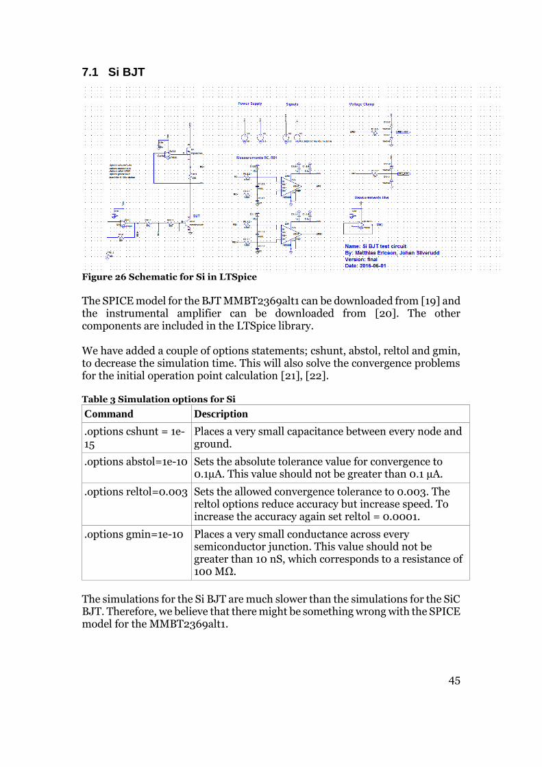
Figure 26 Schematic for Si in LTSpice ....................................................................................45
Figure 27 Simulation results for Si BJT using pulse mode .............................................46
Figure 28 Simulation results for Si BJT using DC sweep ................................................46
Figure 29 Gummel plot from Si BJT ........................................................................................46
Figure 30 Schematic for SiC in LTSpice .................................................................................47
Figure 31 Simulation results for SiC BJT using pulse mode ..........................................48
Figure 32 Simulation results for SiC BJT using DC sweep ..............................................48
Figure 33 Gummel plot from Si BJT ........................................................................................48
Figure 34 Prototype 1 ..................................................................................................................49
Figure 35 Prototype 2 with components added. ...............................................................50
Figure 36 Prototype 3 ..................................................................................................................51
Figure 37 SiC pattern ....................................................................................................................52
Figure 38 Temperature sensor test ........................................................................................53
Figure 39 Si measurement results. From DC sweep ........................................................54
Figure 40 Si measurement results. From pulse mode with slow filter .....................54
Figure 41 Si measurement results. From pulse mode with fast filter .......................55
Figure 42 Results from prototype 3 .......................................................................................56

4
Figure 43 Power consumption Vcc .........................................................................................56
Figure 44 Gummel Log-Linear plot from manual DC sweep .........................................58
Figure 45 Gummel Log-Log plot from manual DC sweep ..............................................58
List of tables
Table 1 Thermal conductivity factors ....................................................................................22
Table 2 Component values for figure 25 ...............................................................................40
Table 3 Simulation options for Si .............................................................................................45
Table 4 Temperature sensor .....................................................................................................53
Table 5 Power consumption ......................................................................................................57

5
List of abbreviations
ADC Analog-to-Digital Converter BJT Bipolar Junction Transistor CAD Computer Aided Design COTS Commercial Off The Shelf DAC Digital-to-Analog Converter DC Direct Current DUT Device Under Test EDA Electronic Design Automation EMC Electromagnetic compatibility EMI Electromagnetic interference IC Integrated Circuit KTH Kungliga Tekniska Högskolan (Royal Institute of Technology) LEO Low Earth Orbit MOSFET Metal Oxide Semiconductor Field Effect Transistor MIST MIniature STudent satellite MCU Microcontroller unit OBC On Board Computer Op-amp Operational Amplifier PCB Printed Circuit Board RDS Resistance across Drain and Source SiC Silicon Carbide SMD Surface Mounted Device SPICE Simulation Program with Integrated Circuit Emphasis TID Total ionizing dose VBE Voltage Base to Emitter VCE Voltage Collector to Emitter VG Voltage level Gate VGS Voltage Gate to Source VS Voltage level Source WOV Working on Venus

6

7
1 Introduction
This chapter gives an introduction to our bachelor thesis and will include the background, goals, and purpose of the project.
1.1 Background
KTH Space Center are as of January 28, 2015, designing a CubeSat miniature satellite. The project is called MIST (MIniature STudent satellite) and gives students an opportunity to develop an actual satellite. The MIST will carry a number of experiments on board:
CubeProp, a propulsion system prototype for CubeSats
RATEX-J, a prototype mass spectrometer
PiezoLEGS, test of piezoelectric linear motor
CUBES, x-ray background explorer
MoreBac, Microfluidic Orbital Resuscitation of Bacteria
SEUD, experiment for a new method for trapping data errors
SiC in Space, an experiment for silicon carbide bipolar junction transistors)[1].
The MIST project is estimated to end in 2017 and the launch is expected to take place shortly after. The satellite will be placed in LEO (Low earth orbit). LEO is defined to be an orbit located between 161 km and 322 km over the earth[2]. The main purpose of SiC in Space is to test and verify that a bipolar junction transistor (BJT) of silicon carbide (SiC) works in space. The experiment is also associated with the Working on Venus project. This is a much larger mission aimed towards sending a number of probes to the surface of Venus. One of the main challenges with landing on Venus is the extreme temperature. The landers would need semiconductors that are very heat resistant. A semiconductor that might be able to withstand Venus environment is SiC. The SiC in Space experiment will help to understand how the SiC BJT behaves in space. BJTs are able to amplify small currents into larger currents. For direct current this characteristic is called the DC current gain, denoted as β. The DC current gain is dependent on several parameters, including the temperature. BJTs made of silicon carbide are able to withstand extreme environments. Previous studies have shown that SiC BJTs remain operational at very high temperatures[3].
1.2 Problem
There are three main differences regarding constructing electronics for use in space compared to on earth[4].
Large temperature variations
Higher dose of radiation
Vacuum We need to be careful with our selection of components since we only are allowed to use COTS (Commercial Off The Shelf) products. The space environment will also make it difficult to test the circuits under its normal

8
operating conditions. The circuits need to be stable and robust as we cannot change anything once the satellite has been launched. The experiments and the satellite itself are powered by solar panels. The solar panels will charge the battery when the satellite is on the light side of the earth. Our experiment needs to be as power efficient as possible so it will not drain the battery. There are also restrictions on the size of the PCB (Printed Circuit Board). The SiC in Space experiment will use the PC104 standard which is 94x90 mm.
1.3 Purpose
The purpose of the SiC in Space experiment is to measure how the environment in low earth orbit affects the DC current gain of a silicon carbide BJT. Particularly how the temperature changes the DC current gain. This thesis describes how the characteristics of a transistor could be measured using analog circuitry. This thesis will also examine some of the environmental challenges of constructing electronics in low earth orbit.
1.4 Goal
Our goal is to be able to construct a prototype on a PCB at the end of the project. The prototype should contain circuitry to measure the DC current gain for both a SiC and a Si BJT. The PCB will need to be constructed together with the two other groups within the SiC in Space project.
1.5 Benefits, Ethics, and Sustainability
The SiC in Space experiment will hopefully aid in our understanding of SiC. Electronics made of SiC handles extreme environments very well. In the future, we might be able to put electronics in an extreme environment, where it is not possible today, for example, in automatic control systems inside engines[5].
1.6 Delimitations
This thesis will implement the SiC BJT as a regular BJT with different values for VBE. It will not try to evaluate the functionality of the SiC BJT. Nor will it explain the physics of the SiC BJT. The SiC in Space project consists of two other theses. The goal of the “Design of microcontroller circuit and measurement software for SiC and Morbac experiment”[6] is to design the software for the microcontroller. “Design of power supplies for Sic and Piezo LEGS experiment”[7] will select the linear DC/DC regulator for the experiment. Therefore, we will refrain from approaching the software design or the selection of the linear DC/DC regulator.

9
1.7 Outline
Chapter 2 Method describes the method we used and how the project was organized. Chapter 3 Theory provides the theoretical background for our design and measurements. Chapter 4 System architecture contains a brief description of the system architecture. Chapter 5 Test circuitry describes the design process for our test circuit, as well as a final version of the test circuit. Chapter 6 Simulations describes how the simulations were conducted and the simulations results. Chapter 7 PCB presents the different prototypes we have developed. Chapter 8 Measurement will present results we have obtained using the measurement circuits. This chapter will also show the power consumption and the calculation of the DC current gain. Chapter 9 Conclusions contains our conclusions together with future work. Appendix A contains datasheets for the components. Appendix B contains schematics from the simulations. Appendix C contains schematics, PCB layout and bill of material for the different prototypes.

10
2 Method
2.1 Duration and location
This bachelor degree project was conducted from 3 March, 2016, to 3 June, 2016, which corresponds to 10 weeks of full-time studies. The project was carried out at ICT-KTH in Kista, Stockholm. During the degree project, we had access to one classroom as well as an electronics laboratory.
2.2 Organization
The SiC in Space project was divided into three different degree projects. The SiC in Space worked close together but each group was focusing on different parts of the experiments. Our group has been focusing on the test circuits and how the different characteristics of BJTs could be measured.
The two other groups were responsible for the microcontroller and the DC/DC converter for the test circuitry. The microcontroller group selected and designed the software for the experiment. This included the communication with the OBC (On Board Computer). They also assisted the MoreBac experiment. The DC/DC converter group made the selections of a suitable DC/DC converter for the SiC in Space experiment, as well as another DC/DC converter for the PiezoLEGS experiment.
An interface between the different parts of the project had to be determined. The interface would enable the groups to work separately on their own. Without a defined interface the project should not be able to progress. A large part of the interface was already determined at the start of the project.
2.3 Literature
Our project started out with a literature study which lasted three weeks. The focus of the literature study was to see how to the environment in LEO (Low Earth Orbit) would affect the circuit design, specifically how a component's temperature could be measured in LEO. We also did some research on what type of components or materials to avoid. Finally, we studied semiconductors like BJT and diodes, since this project involved a lot of analog electronics.
2.4 Circuit design
We have mostly used an empirical design approach as a basic measurement circuit is simple to design. The difficult part is to make it robust, low power and knowing what types of components we can use in LEO. By making simulations and then analyzing the results we were steadily able to improve our circuit design.
2.5 Software
We have used LTSpice for our simulations. LTSpice is a freeware SPICE simulator developed by Linear Technology. LTSpice has both a schematic

11
viewer and a waveform viewer. It is also possible to add third party SPICE models to the software. To design the PCB we have been using Diptrace. Diptrace is an EDA/CAD program. The program enables the design of schematics, PCB layouts and components patterns. The files can then be exported as Gerber files. We have been using a freeware version of the program limiting us to two layer PCBs. We have been using Mathematica to generate graphs.
2.6 Testing
A simple starting point would be to use a breadboard. The breadboard would be something in between the simulator and a PCB, enabling us to use the intended components. It is also very simple to change the circuit design on a breadboard if needed. It is, therefore, be a good step to take before doing a PCB.
A PCB is necessary to design. After all, the experiment will be on a PCB someday. A PCB has very little room for changes once it has been produced. Simulations and a breadboard need to be used before any PCB goes into manufacturing. The manufacturing of a PCB could be done locally at KTH, as there is a milling machine at KTH. This method is also relatively fast. If time permits we could let a professional PCB company manufacture our prototypes. However, this could prove time consuming. The more the project progresses, the more we expect to use a PCB to test our circuit. At the end of the project, we expect to put together a PCB which includes the work of all groups in SiC in Space. This would enable us to do a final system test.

12
3 Theory
3.1 Bipolar Junction Transistor
A bipolar junction transistor (BJT) is a component that enables a small current to control a larger current. The BJT is made up of a semiconducting material. This material is typically silicon, but this experiment will also involve BJTs that are made of silicon carbide. A BJT consist of three different connectors; the base, the collector, and the emitter. These are doped in a way so they form pn-junctions between the base and collector, respectively between the base and emitter.
Figure 1 BJT with base and collector resistors
The current through a diode can be described by the Shockley diode equation. This is an exponential function given by:
𝐼 = 𝐼𝑆(𝑒𝑉𝐷
𝑛∗𝑉𝑇 − 1) (3.1)
I is the current through the diode, IS is the reverse bias saturation current, VD is the voltage across the diode, VT is the thermal voltage and n is an ideality factor. This means that a small change in the voltage across the diode results in a much larger change in current through the diode. The base-emitter junction is basically a diode. The base-emitter voltage will remain approximately the same for different currents because of the exponential nature of a diode. The VBE of the silicon carbide BJT will differ

13
greatly from the silicon BJT. The base-emitter voltage of the SiC BJT is about 2.5 V compared to the base-emitter voltage of silicon, which is 0.7 V. The base current will be amplified as a larger collector current by the BJT. The relationship between the collector current and base current is called the DC current gain, β. 𝐼𝐶 = 𝛽 ∗ 𝐼𝐵 (3.2)
𝛽 =𝐼𝐶
𝐼𝐵
(3.3)
It is possible to bias the BJT with a voltage source by adding a resistor to the base. The current through the resistor increases linearly with the voltage across it. This will make the base current much easier to control.
𝐼𝐵 =𝑉𝑖𝑛 − 𝑉𝐵𝐸
𝑅𝐵
(3.4)
3.2 Operational Amplifier
An operational amplifier (op-amp) is a component that initially was used for calculating different arithmetic operations. An operational amplifier can also be used for calculation derivation and integration. There are more than mathematical uses for an op-amp, as will be shown subsequently.
Figure 2 Operational amplifier
An op-amp has two inputs and one output. The outputs are called the inverting and non-inverting inputs (See figure 2). An ideal model of an op-amp can be used when designing circuits by hand. The ideal model gives a good approximation of the real op-amp.
Infinite amplification
Infinite input resistance
No output resistance
The op-amp can be viewed as a dependent voltage source which depends on the two inputs.

14
The voltage difference between the inverting and the non-inverting inputs will be amplified and sent to the output. The output is limited to the supply voltage and will obviously not reach infinity. This will make the op-amp work as a comparator.
Figure 3 Operational amplifier internal
𝐴(𝑉+ − 𝑉−) = 𝑉𝑜𝑢𝑡 (3.5) If the voltage of the non-inverting input is greater than the voltage of the inverting input, the output will equal the positive supply of the op-amp. If however the inverting input is greater than the non-inverting input, the output will equal the negative supply instead. To obtain any other function than a comparator a feedback loop is needed. Feedback is when an output signal, or a part of it, is fed back to the inputs. The functions needed in the test circuits are:
Amplifier
Buffer
Differential amplifier
Negative feedback is needed in in order to get these functions. It means that the output is fed back into the inverting input. This will cause the op-amp to drive the voltages of the inputs close together. If there is a difference between the input voltages, the output will respond in a way that eliminates the difference.

15
3.2.1 Non-inverting amplifier
Figure 4 Non-inverting amplifier
The signal that is going to be amplified should be fed into the non-inverting input. 𝑉𝑖𝑛 = 𝑉+ (3.6)
This causes the output react in such a way that the voltages on the inputs are kept at the same level. 𝑉− = 𝑉+ (3.7)
Since the voltage over R1 is known, it could easily be calculated. 𝑉− = 𝑅1 ∗ 𝐼𝑜𝑢𝑡 (3.8)
The current that goes in the feedback loop is the same for the both resistors. Because of the infinite input resistance on the op-amp. The current will affect the voltages over the resistors, which in turn become the output voltage. 𝑉𝑜𝑢𝑡 = 𝐼𝑜𝑢𝑡(𝑅1 + 𝑅2) (3.9)
The amplification of a signal is the ratio between the output and input signal. How great the amplification is depends solely on the resistors.
𝑉𝑜𝑢𝑡 = 𝑉− 𝑅1 + 𝑅2
𝑅1
(3.10)
𝐴𝑉 =𝑉𝑜𝑢𝑡
𝑉𝑖𝑛=
𝑅1 + 𝑅2
𝑅1
(3.11)

16
3.2.2 Inverting amplifier
Figure 5 Inverting amplifier
The current that flows through the R1 resistor has to equal the current that flows through the R2 resistor, since no current flows into an ideal op-amp. The current that flows through R1 is determined by the voltage over R1, divided by its resistance. 𝑉𝑖𝑛 − 𝑉−
𝑅1=
𝑉− − 𝑉𝑜𝑢𝑡
𝑅2
(3.12)
If the non-inverting input is connected to ground it will force the inverting input to be grounded as well. Knowing this, the expression could be further simplified. 𝑉𝑖𝑛 − 0
𝑅1=
0 − 𝑉𝑜𝑢𝑡
𝑅2
(3.13)
𝐴𝑉 =𝑉𝑜𝑢𝑡
𝑉𝑖𝑛= −
𝑅2
𝑅1
(3.14)
The amplification of an inverting amplifier depends on the ratio between R1 and R2. Note that the inverting amplifier will provide a negative amplification.

17
3.2.3 Buffer
Figure 6 Buffer with Op-Amp
If the op-amp has no other components in the feedback loop it becomes a buffer. The buffer does not change the input signal in any way. There are more reasons of using an op-amp than for amplifying signals. As mentioned before, an op-amp has a very high input resistance and a very low output resistance. These features are very important to ensure accurate voltage measurements. This experiment will get its data entirely through voltage readings. It is, therefore, important to provide as accurate readings as possible.
The voltage difference between the two input terminals is amplified and presented on the output as mentioned before. 𝑉𝑜𝑢𝑡 = 𝐴(𝑉+ − 𝑉−) (3.5)
This causes the inverting output to have the same voltage as the output.
𝑉− = 𝑉𝑜𝑢𝑡 (3.15)
This will be amplified as before.
𝑉𝑜𝑢𝑡 = 𝐴(𝑉+ − 𝑉𝑜𝑢𝑡) (3.16)
The expression can be rewritten as below to show how the output depends on the non-inverting input.
𝑉𝑜𝑢𝑡 +
𝑉𝑜𝑢𝑡
𝐴= 𝑉+
(3.17)
The fraction on the left-hand side approaches zero because of the high amplification of the op-amp. The expression could, therefore, be simplified even further.
𝑉𝑜𝑢𝑡 = 𝑉+ (3.18)
As can be seen, the output of a buffer will obtain the value of its input.

18
3.2.4 Differential amplifier
Figure 7 Differential amplifier
A differential amplifier delivers an output that corresponds to the voltage difference between the two inputs.
𝑉+ = 𝑉𝐵
𝑅4
𝑅3 + 𝑅4
(3.19)
𝑉− = 𝑉+ (3.7)
The current that flows through R2 are the same as the one that flows through R1. 𝑉𝐴 − 𝑉𝐵
𝑅4
𝑅3 + 𝑅4
𝑅2=
𝑉𝐵𝑅4
𝑅3 + 𝑅4− 𝑉𝑜𝑢𝑡
𝑅1
(3.20)
This expression could be rewritten to obtain the output voltage.
𝑉𝑜𝑢𝑡 =
𝑅1
𝑅2(𝑅1 + 𝑅2
𝑅1𝑉𝐵
𝑅4
𝑅3 + 𝑅4− 𝑉𝐴)
(3.21)
If the resistance of R1 equals the resistance of R4 and the resistance of R2 equals the resistance of R3, this turns out to be a simple expression.
𝑉𝑜𝑢𝑡 =𝑅1
𝑅2(𝑉𝐵 − 𝑉𝐴)
(3.22)
If the resistances of R1 and R2 are equal, the output voltage will be the actual voltage difference between the inputs. 𝑉𝑜𝑢𝑡 = 𝑉𝐵 − 𝑉𝐴 (3.23)

19
This experiment will measure voltages across resistors in which differential amplifiers will come in handy. Instead of measuring the voltage before and after a resistor using an ADC, and calculating the difference using an MCU, the difference could be obtained instantly. This will reduce the number of ADCs needed and simplify the work of the MCU.
It is important to dimension the resistors correctly. Firstly, if they are selected too small the differential amplifier will draw an unnecessary large current. This is not preferable since the experiment will operate on a satellite. Secondly, if the resistor ratios are not fully matched the differential amplifier will not produce a correct result. All the resistors in the differential amplifier have to be equal in order to get the actual voltage difference of the inputs. Thirdly, there are limitations on the size of the PCB. The size of the final PCB will be according to the PC104 standard which limits the size down to 90x94 mm. In order to use an op-amp as a differential amplifier, it requires four external resistors. Since the experiment measures the voltages across the resistors base and collector for both the silicon and the silicon carbide transistors, this will result in four differential amplifiers and 16 resistors.
There is, however, another drawback to be taken into account when using a differential amplifier. The input resistance of a differential amplifier is very low and differs between the inputs. The input resistance of the non-inverting input is: 𝑅𝐼𝑁+ = 𝑅3 + 𝑅4 (3.24)
The input resistance of the inverting input will vary depending on the voltage of the non-inverting input.
𝑉+ = 𝑉𝐵
𝑅4
𝑅3 + 𝑅4
(3.20)
𝑉− = 𝑉+ (3.7)
𝑉− = 𝑉𝐵
𝑅4
𝑅3 + 𝑅4
(3.25)
𝐼𝑅2 =𝑉𝐴 − 𝑉𝐵
𝑅4
𝑅3 + 𝑅4
𝑅2
(3.26)
𝑅𝐼𝑁− =𝑉𝐴
𝐼𝑅2=
𝑉𝐴
𝑉𝐴 −𝑉𝐵 𝑅4
𝑅3 + 𝑅4
𝑅2
(3.27)

20
𝑅𝐼𝑁− = 𝑅2
𝑉𝐴
𝑉𝐴 −𝑉𝐵 𝑅4
𝑅3 + 𝑅4
(3.28)
As can be seen, the input resistance will vary. The input resistance will be parallel to the resistance in which we will measure the voltage across. This will be a problem when performing measurements due to the varying signals.
3.2.5 Instrumental amplifier
Fortunately, there is a component that offers the function of a differential amplifier but is better suited for our purpose. This component is called an instrumental amplifier. An instrumental amplifier consists of three op-amps.
Figure 8 Instrumental amplifier
The circuit looks quite familiar to what was described earlier in 3.2.3 and 3.2.4. By adding buffer stages to the inputs the instrumental amplifier will have a high, and constant input resistance. The output voltage can be calculated with superposition, by first calculating each input contribution separately and then adding them together.
𝑉𝑜𝑢𝑡 = (𝑉2 − 𝑉1)𝑅3
𝑅2(1 +
2𝑅1
𝑅𝐺)
(3.29)
If R3 equals R2 we get a simpler expression.
𝑉𝑜𝑢𝑡 = (𝑉2 − 𝑉1)(1 +2𝑅1
𝑅𝐺)
(3.30)
When bought as an IC (Integrated Circuit) only the RG resistor needs to be added. The other resistors are already matched and the feedback network is

21
contained on the inside of the IC. The RG resistor will control the gain to the output. If RG is much larger than R1 the gain will be 1. This can also be achieved by removing the RG completely. 𝑉𝑜𝑢𝑡 = 𝑉2 − 𝑉1 (3.31)
Our intention is to use the instrumental amplifier as a differential amplifier with buffers on the inputs. An instrumental amplifier offers great performance when it comes to measurements. It is a very convenient solution to use because it does not require much work from the user to get it up and running. The resistors are already matched and the feedback network is contained on the inside of the IC, and the gain is easily controlled with RG. We could, therefore, focus solely on selecting an instrumental amplifier that meets our requirements by comparing datasheets.
3.3 Temperature
There are three different ways heat can be transferred by; radiation, conduction, and convection [8]. By radiation the heat is transferred as electromagnetic radiation from the object’s surface, by conduction heat is transferred through a material and by convection the heat is transferred through a fluid or gas.
An object which absorbs all incoming electromagnetic radiation is called a black body. A black body is, therefore, a perfect emitter. An object which does not absorb all of the incoming radiations, but reflects parts of the radiation is called a gray body. For example, the sun is approximately a black body and the earth is a gray body.
Radiation emitted by a body is given by Stefan-Boltzmann law:
𝑄 = 𝜀𝜎𝐴𝑟𝑇4 (3.32) Where 𝜎 is Stefan-Boltzmann constant, Ar is the radiating surface area, T is the temperature in Kelvin and ɛ is a ratio between what the body emits and what it would have emitted if it were a black body. Therefore ɛ equals one for a black body.
Heat is energy generated by moving particles. When the temperature rises the particles movement increases. Heat can be transferred through a material by particles colliding. This is called thermal conduction.
Fourier’s law gives the amount of energy that flows through a unit area per unit time: �⃑� = −𝑘𝛻𝑇 (3.33)

22
q is the amount of energy(heat) that flows through a unit area per unit time. q is a vector which means that it describes the heat’s magnitude and direction. k is the material's thermal conductivity. ∇T is the temperature gradient. The temperature T can be described as a scalar field in three dimensions(𝑥, 𝑦, 𝑧). ∇T is given by:
𝛻𝑇 = 𝜕𝑇
𝜕𝑥𝑖 +
𝜕𝑇
𝜕𝑦𝑗 +
𝜕𝑇
𝜕𝑧𝑘
(3.34)
i, j and k are the unit vectors. This means that ∇T is a vector field where each point is a vector pointing in the warmest direction. And -∇T vector field where each point is a vector pointing in the coldest direction. Therefore, we can assume that heat will move in the same directions in all materials. But the rate of heat transfer is determined by the thermal conductivity.
The material’s conductivity varies a lot between different materials. Table 1 Thermal conductivity factors [9]
Materials K (W/m°K) K (W/in°C)
Copper 355 9
Aluminum 175 4.44
FR4 .25 0.006
Solder 63/67 39 1
Air .0275 0.0007
Table 1 shows the conductivities for different materials. High conductivity means that heat is easily transferred through the material. As shown by Table 1 metals like copper and aluminum transfers heat much better than the FR4 laminate. Another way to compare how good a material transfer heat is to calculate thermal conductance GT or the thermal resistance RT.
𝐺𝑡 =𝐿
𝑘 ∗ 𝑊 ∗ 𝑡=
𝐿
𝑘 ∗ 𝐴𝐶𝑆
(3.35)
𝑅𝑡 =𝑘 ∗ 𝑊 ∗ 𝑡
𝐿=
𝑘 ∗ 𝐴𝐶𝑆
𝐿
(3.36)

23
Where k is the thermal conductivity, L is the length, W is the width, t is the thickness and Acs is the area cross section of the heat flow. Since the atmosphere is very thin in the satellite’s orbit, convection will virtually have no effect on the satellites temperature[8]. This differs from earth where heat is transferred away from the electrical components through the air.

24
4 System architecture
The SiC in Space project consists of three different bachelor degree projects. Each project designs different part of the experiment. This section will describe briefly what part each project will design.
Figure 9 System architecture
4.1 DC/DC converter
The linear regulator LT3062 has been selected as the DC/DC converter which will convert the battery voltage of 14 V down to 10 V. The SiC in Space experiment will be shut down by using a shutdown pin on the LT3062. This pin is controlled by the microcontroller. The design of the DC/DC converter is covered in[7] .
4.2 Test circuitry
The test circuitry will bias and measure the SiC and Si BJTs. It should be possible to change the base current and the VCE voltage. The microcontroller will read the measurement as voltage. The collector and base currents will be measured as voltage and calculated afterward. This is done by measuring the voltage drop across a known resistance. The VBE will be measured directly as a voltage, since it does not need any conversion. The temperature will also be measured as a voltage. This voltage needs to be converted to degrees Celsius through calculation or by using a lookup table. The test circuits will be biased by two inputs. VIN sets the base current and the VCESet sets the VCE voltage. Both inputs are analog, and therefore, they need a continuous signal to bias the circuit.

25
The test circuit is supplied with 10 V by the DC/DC converter. The test circuits are also shut down by shutting down the DC/DC converter. This is controlled by the microcontroller.
4.3 Microcontroller
The microcontroller is responsible for reading the measurement, control the biasing, start and shut down the experiment and communicating with the rest of the satellite. The STM32L053C8T6 from STMicroelectronics will be used for this project. The STM32L053C8T6 has ten ADCs for reading the measurements, and one DAC to control the biasing. The software design and selection of the microcontroller for the SiC in Space experiment is covered in [6].

26
5 Test circuits
This chapter will describe the design processes, the components we have used and why we selected them. We want to use as small currents as possible so that our experiment will not drain the battery. The test circuit needs to be robust and have low complexity to minimize the risk of failure.
To measure the base and collector current the experiment measures the voltage drops across different resistors. These voltage drops can in turn be measured by the ADCs of the microcontroller.
5.1 Supply voltage
5.1.1 Power matrix
There are two power matrices on the MIST satellite; one with 3.3 V and one with 5 V. The different experiments will be connected to either the 3.3 V or the 5 V matrix. It has not yet been decided by MIST which power matrix SiC in Space will be connected to. Both voltage levels are too low for the SiC BJT, but they might work for the Si BJT. However, to keep the circuitry for the SiC BJT and the Si BJT as similar as possible we will just use the same supply voltage for both transistors. The microcontroller operates at 3.3 V. If the experiment is connected to the 5 V power supply the microcontroller needs to be supplied through a 3.3 V linear DC/DC converter.
5.1.2 Linear DC/DC converter from battery power
The MIST satellite will be powered by solar panels when in orbit. The solar panels will charge a battery. The battery will deliver a voltage between 12 V and 14 V. To operate the SiC BJT the experiment needs around 10 V. By using a linear DC/DC converter we can convert the battery voltage down to 10 V. This is the goal of [7].
5.1.3 Decoupling capacitors
To increase the stability of the power supply the experiment will have decoupling capacitors between the power rail and ground. The decoupling capacitors act as small power reservoirs in case the supply voltage should drop. If so, the power collected within the capacitor will discharge to keep the voltage from decreasing. The decoupling capacitors can also act as short circuits for rapid changes in voltage. If a transient in the form of a voltage spike would propagate through the power supply it would be connected directly to ground. Thus protecting the circuitry. Usually, different components are decoupled separately. The decoupling capacitors are placed as close to the component they are supposed to decouple. The size of the decoupling capacitors is typically found in the components

27
datasheet. Sometimes the manufacturer also provides a recommended PCB layout for decoupling. In our design we have used the decoupling capacitors recommendations found the in the datasheets from the manufacturers.
5.2 Adjustable settings
We want the test circuit to be able to run in different modes. The idea is to let the microcontroller set the base current. This will also change the collector current. In the following sections, we will present various solutions.
5.2.1 Switches
Figure 10 Simple bias BJT
The simplest way to biasing a BJT is to add a resistor between a voltage source and the base. This will enable a current flowing through the base. The base current is dependent on the size of RB since VBE is almost constant. The base current will in turn control the collector current. The collector current could be measured by measuring the voltage across the collector resistor. The base current can be made adjustable by adding more RB resistors and controlling them with switches.

28
Figure 11 Adjustable base current with switches
MOSFETs makes good switches since they are controlled with voltage and not current like BJTs. It is important where the switches are placed since the position of the switch decides whether we need to use a high or a low side switch. A low side switch is located close to the ground and a high side switch is located close to VCC.
Figure 12 High and low side switches
The difficulty arises when the switch is shut off. Since RDS is very small (between 10 mΩ to 10 Ω) compared to RB (a couple of kΩ), most of the VCC voltage will be distributed across RB. This is not a problem for a low side switch. To turn the MOSFET on again the gate-source voltage needs to be greater than the threshold voltage.

29
𝑉𝐺𝑆 > 𝑉𝑡ℎ (5.1)
⇒ 𝑉𝐺 > 𝑉𝑡ℎ + 𝑉𝐵𝐸 = 𝐸𝑛 > 𝑉𝑡ℎ + 𝑉𝐵𝐸 (5.2)
Figure 13 Adjustable base current with low side switches
For the high side switch, VS is approximately VCC. 𝑉𝐺𝑆 > 𝑉𝐶𝐶 + 𝑉𝑡ℎ (5.3)
Figure 14 High side switch
This is solved by using two MOSFETs; one with p-channel and one with n-channel (see figure 14). When En is low, Q1 is off and Q2 VGS gets pulled to VCC.

30
This means that Q2 is also off. When En is high, current will flow through R1 down to ground. If the voltage drop over R1 is high enough Q2 VGS will drop below Vth and get turned on.
Figure 15 Adjustable base current with high side switches
The main issue with this solution is that we need a lot of components and signaling lines whereas the space on the PCB is limited. For the high side switch, we need to draw a current through the R1 resistor. This will increase our power consumption.
5.2.2 Current generator
Another simple solution is to use a current generator to set the base current. The current generator will generate a very precise current. This means that it is not necessary to measure the base current by measuring the voltage drop across the base resistor. The problem with using a current generator is the component itself. Some are too advanced and others need external components we cannot use. More advanced current generators have their own microcontroller controlling the component and handling the communication interface (usually I2C or SPI). This is an added complexity we do not want, as we want the test circuit to be as robust and stable as possible. The added complexity might introduce more parameters which may fail. More simple current generators work by adding an external resistor to control the output current. By using a digital potentiometer it is possible to change the output current. However, digital potentiometers are sensitive to vibrations and they will probably not function well after the launch.

31
5.2.3 Using a DAC
A simple solution which does not increase the complexity of circuitry is to use a digital-to-analog converter (DAC) on the microcontroller and add a resistor to the base of the BJT. The DAC outputs a voltage between 0.2 V - 3.1 V with 12-bits resolution. The DAC can deliver a current up to 16mA, which is more than enough. The output voltage from the DAC is divided between the resistor and VBE.
𝐼𝐵 =𝑉𝑖𝑛 − 𝑉𝐵𝐸
𝑅𝐵
(3.4)
Figure 16 Adjustable base current with DAC
This might work fine for the Si BJT since VBE is only around 0.7 V. However, for the SiC BJT VBE is closer to 2.5 V. This means that the experiment only can use a small interval of the DAC to set the base current.
5.2.4 Using a DAC with operational amplifier
By using a DAC together with an amplifier the experiment can use a larger interval of the DAC output. By connecting an op-amp to the 10 V power supply it is possible to get much larger input signals. To avoid saturating the op-amp the gain should not be greater than 10 / 3.1 ≈ 3.2. To measure base current the experiment needs to use a voltage divider since the input signal will be too large to measure once it has been amplified. It will also be easier to calculate the power consumption since the base current will be drawn from the op-amp and not the microcontroller.
5.2.5 Constant collector-emitter voltage
The DC current gain is not only depending on the temperature. It also dependent on the collector-emitter voltage, VCE. For a small VCE voltage, the DC current gain increases with VCE. After a certain point, the VCE voltage has little impact on the DC current gain. The point at which this happens differs between different BJTs, but it is usually around 0.4 V for a regular small-signal BJT.

32
Figure 17 The relationship between IC, IB, and VCE.
Measured on the MMBT2369ALT1G (Si BJT)
To set a constant VCE we use an op-amp, together with an n-channel MOSFET. The MOSFET and RC are connected in the negative feedback loop. The idea is to set VCE with the non-inverting input of the op-amp. IC (and therefore the voltage across RC) will still be controlled by IB. The remaining voltage from VCC will be distributed across the MOSFET’s VDS and the RC. This makes VCE adjustable. However, since the microcontroller only has one DAC we will connect VCESET to VDD 3.3 V.
Figure 18 Constant VCE with feedback loop

33
5.3 Measurement
The microcontroller has ten ADC inputs to measure voltage. Each BJT has three measurement points and one temperature sensor. This is eight measurements in total. Since the microcontroller is supplied by 3.3 V the ADC can only measure voltages in the interval 0 V- 3.3 V. The following sections will describe different couplings used to measure the currents and voltage levels for the BJTs.
5.3.1 Voltage divider
Figure 19 Adjustable base current with DAC together with amplifier and measurement points
The microcontroller output is only able to provide voltages up to 3.1 V. This will greatly limit the range of possible settings since the output voltage needs to be larger than the BJT’s base-emitter voltage. This is usually around 0.7 V for silicon and 2.5 V for silicon carbide. To increase the interval of useful DAC outputs the output signal is amplified about 3 times, giving the output signal a range up to 9.3 V.
There might be problems when the microcontroller wants to read the voltage across the resistor. If the microcontroller is providing 3.1 V, it means that the output of the amplifier will be about 9.3 V. The 9.3 V are then distributed across the resistor and the base-emitter-junction. This causes the voltage across the resistor to be approximately 8.6 V if the BJT is made of silicon. The microcontroller can only measure voltages up to its supply voltage of 3.3 V. A voltage divider could be used in order to solve this problem.
Figure 20 Adjustable base current with DAC. Together with amplifier and measurement with voltage divider
This causes the voltage that previously were across the single resistor to be spread out over two resistors.

34
𝑅 = 𝑅1 + 𝑅2 (5.4)
Since the resistance of the previous resistor equals the total resistance of R1 and R2, the current then stays the same.
𝐼𝑅 =𝑉𝑅
𝑅
(5.5)
The voltage across R1 is given by its resistance multiplied by the current that flows through it. 𝑉𝑅1 = 𝑅1 ∗ 𝐼𝑅 (5.6)
If the expression is rewritten as below, it is easy to see how the relation between the R1 and R2 resistor will affect the voltage across each resistor.
𝑉𝑅1 = 𝑉𝑅 ∗ 𝑅1
𝑅1 + 𝑅2
(5.7)
The reason to use a voltage divider is to reduce the voltage across the resistor that the microcontroller is measuring the voltage over. A suitable voltage divider would ensure that the microcontroller would not get voltages over 3.3 V. The maximum voltage across R1 should, therefore, be around 3.3 V. If the resistance of R2 is twice the resistance of R1, the voltage across R1 would be a less than a third of 9.3 V.
5.3.2 Buffer
One of the difficulties with measuring current or voltages is that the measuring itself has an effect on the result. A solution is to add buffers between the ADCs and the measurement points. Since the op-amp and measuring object are not connected in series the voltage at the measuring point will stay the same. This is due to the high input resistance of the op-amp (a couple of MΩ). The current through the object that will be measured will stay unaffected. The op-amp only needs a small bias current of usually a couple of nA. The issue with using only a buffer is that the voltage at the measuring point has to be lower than 3.3 V. A better solution is presented in section 5.3.3. However, we can use a buffer to measure the VBE. The base-emitter voltage will be around 0.7 V for the Si BJT and about 2.5 V for the SiC BJT.
5.3.3 Instrumental amplifier
The instrumental amplifier outputs the voltage difference between two points. This makes it possible to measure voltage levels over 3.3 V, as long as the difference between the points is between 0 V- 3.3 V. Instrumental amplifiers have very high input resistance and only draw a small bias current, making them good for measurements. The instrumental amplifier will give the voltage

35
difference as a single voltage on its output. This makes it easier for the ADC to read the voltage across a particular resistor. The MCU can obtain the difference straight away instead of measuring two points using two ADC each and then calculating the difference.
Figure 21 DAC with voltage divider
There are limitations on the size of the PCB. The size of the final PCB will be according to the PC104 standard which limits the size down to 90x94 mm. In order to use an op-amp as a differential amplifier would require four external resistors to set up. Since the experiment measures the voltages across the resistors base and collector for both the silicon and the silicon carbide transistors, it will result in four differential amplifiers and 16 resistors. By using the instrumental amplifier we will save space on the PCB.
5.3.4 Temperature measurement
Changes in temperature can affect the behavior of semiconductors. Therefore, it is interesting for the experiment to measure the temperature of the BJTs. The temperature measurement of the BJTs in space differs from how it could be done on earth. The atmosphere in low earth orbit is very thin which greatly reduces the impact of the thermal convection[8].
The PCB mainly consist of the two materials; copper and FR-4 laminate. Copper is a much better heat conductor than the FR-4 laminate. If a BJT is placed close to a temperature sensor, its heat could spread through the copper traces. This type of heat transportation is called thermal conduction. The other type of heat transfer is radiation. The radiated heat will probably be much smaller than the conducted heat due to the small area surface of the SiC BJT.

36
Figure 22 SiC pattern on PCB
The picture displays a subsection of a prototype. The SiC transistor will be glued upon the big square in the middle (1). The square is 7x7 mm to give a sense of its size. On its right-hand side is the temperature sensor (2). Between them is a thick copper trace. (3) is connected to the ground via the sensor. This copper trace is intended to work as a transportation medium for the heat. Even though the (3) is connected to ground, the SiC BJT is not connected to ground through (1). The same method will be used for the Si BJT. Note that the copper plane near the BJT has been removed.
We have not been able to test this method. Therefore, this needs to be further investigated in future work.
5.3.5 Over voltage protection
The instrumental amplifiers need to be connected to the 10 V VCC. This means that they are able to provide up to 10 V on the ADCs. According to STM32l053C8T6’s datasheet, the maximum input voltage is 7.4 V. A voltage spike from the instrumental amplifier output might damage the ADC. To protect the ADC voltage clamps will be used.
Figure 23 Voltage clamp

37
If the voltage level at the ADC input gets larger than the VDD of 3.3 V, the diode connected to VDD will start to draw a current. The diode will not draw any significant current until the voltage across it is approximately 0.7 V, due to the exponential nature of the diode. The current will cause a voltage drop across the resistor R, thus lowering the ADC input voltage. The same thing will happen with the diode connected to ground if the ADC input voltage drops below ground.
The two diodes are present at the ADC input of the microcontroller according to the microcontroller’s datasheet. However, we don’t know how to dimension the resistance since our knowledge of the microcontroller is limited. Therefore, we have added an additional voltage clamp on the ADC input which might turn out to be redundant.
5.3.6 Measuring using pulsed mode
Due to self-heating the experiment might have to conduct measurements in pulses[5], [9]. This is easily done in the software. Self-heating is mainly a concern for the SiC BJT. But we should use the same measuring technique for both BJTs. We have however not been able to perform any tests on the SiC BJT. Therefore, we do not know if this is something we need to concern ourselves with. Self-heating might not actually be a problem since we use very small currents.
5.4 EMC
Electrical components can emit electromagnetic energy through radiation or conduction. This electromagnetic energy can interfere with other electrical components. EMC (Electromagnetic compatibility) is divided into two classes; immunity and emission. Immunity means that a component must be able to resist a certain amount of EMI (Electromagnetic interference). Emission means that a component cannot generate an interference larger than a certain amount. There are four main types of coupling:
Conductive coupling occurs when an interference couples through direct electrical connections.
Inductive coupling occurs when the interference couples through a magnetic field.
Capacitive coupling occurs when an interference couples through an electric field.
Radiative coupling occurs when an interference is introduced through an electromagnetic field.
We have followed the guidelines for EMC provided in the datasheets.

38
5.4.1 Immunity
To increases our circuits immunity we have added a low pass filter on the instrumental amplifier’s inputs. This will reduce noise from RFI (Radio frequency interference).
Figure 24 Low pass filter on instrumental amplifier input
We used CC= 47 pF, CD = 470 pF and R = 4.02 kΩ. CD should at least be 10 greater than Cc. According to the datasheet, the cut-off frequency should be.
𝑓𝑑𝑖𝑓𝑓 =1
2𝜋𝑅(2𝐶𝐷 + 𝐶𝐶)= 40 𝑘𝐻𝑧
(5.8)
𝑓𝐶𝑀 =1
2𝜋𝑅𝐶𝐶= 842 𝑘𝐻𝑧
(5.9)
Immunity needs to be investigated further since we do not know how many experiments will run at the same time. Nor do we know if the satellite will transmit data while the SiC in Space experiment is running. This experiment will also contain a switching DC/DC converter on the PCB. This will cause interference. We do not know if the filter is necessary or not. On the other hand, if the interference will show to have a larger impact than expected, similar filters might be needed to be put on the op-amps.

39
5.4.2 Emissions
During most part of the time the circuit will use DC. This does not necessarily mean that our emissions will be small. The input signal Vin from the microcontroller has a fairly fast rise time of about 3 µs[6]. Its settling time is between 7 µs – 12 µs according to the datasheet. The op-amps have a slew rate of 0.4 V/µs. This means that the op-amps can keep up with the DAC for small changes in voltage.
trise = 1.2
0.4= 3 µ𝑠
(5.10)
⇒ 𝑡𝑟𝑖𝑠𝑒 ≤ 3 µ𝑠 , 𝑤ℎ𝑒𝑛 𝑉𝑑𝑖𝑓𝑓𝑒𝑟𝑒𝑛𝑐𝑒 ≥ 1.2 𝑉 (5.11)
The base and collector will change with the same speed as the input signal since the transistors are faster than the op-amps. The filter on the instrumental amplifier stops the fast signal to propagate any further. When designing the layout on the PCB the switching on the Vin signal needs to be taken into account. The fast signal traces should be kept short. The traces can also be separated by a grounded trace to reduce the emission. It is also important to try to minimize the loops between the signal traces and the ground.

40
5.5 Conclusion
Figure 25 Final test circuit design
Table 2 Component values for figure 25
Name Value Si Value SiC Units Comment VCC 10 10 V Power supply VDD 3.3 3.3 V Power supply R1 10k 10k Ω Amplification R2 22k 22k Ω Amplification RFILTER 4.02k 4.02k Ω RFI-Filter CC 47p 47p F RFI-Filter CD 470p 470p F RFI-Filter RVC 10k 10k Ω Voltage Clamp RB1 47k 16k Ω Base Resistor RB2 100k 22k Ω Base Resistor RC 300 510 Ω Collector Resistor
Schematics, PCB layout, bill of materials and simulations can be found in the appendix.

41
6 Selection of components
This chapter will go through the restrictions we have when selecting different components. This section will present the different components we selected and why we have selected them.
6.1 Restrictions
We are not able to use any specially manufactured components or space graded components. The one exception is the SiC BJT which will be manufactured at KTH ICT. The experiment needs to be built using COTS products. This does not need to be a problem. “Design of a cubesat computer architecture using COTS hardware for terrestrial thermal imaging”[10] shows that it is possible to construct a successful CubeSat using COTS. Ionized radiation will not be an issue. According to simulations done by the MIST team the satellite will only experience a TID (Total ionizing dose) of about 0.66 Gy - 1.38 Gy [11]. Most commercial products are tolerant to about 20 Gy – 100 Gy[12]. Some components can be assumed to have a tolerance of at least 300Gy[13]. This includes anything not containing a semiconductor, BJT, or single junction diodes. This is a very high tolerance for a commercial product, compared to a product graded as radiation tolerant (200 Gy – 500 Gy) or radiation hardened (2 kGy – 10 kGy)[12]. Some types of components should be avoided due to the special environment in LEO. This includes components which do not work in a vacuum or that are sensitive to vibrations. For example, potentiometers accuracy deteriorate when exposed to heavy vibrations. The SiC in Space team has expressed the needs of a list with component types that should be avoided to the MIST team. There is currently a draft contain different materials which should be avoided. This includes among other metals lead and antimony for softening solder. It might be an issue using solders just containing Sn (tin) since alloys containing a high concentration of Sn may develop Sn whiskers[14]. Sn whiskers are small hair-like structures growing out of the Sn surface, hence the name. Sn whiskers are actually able to, at worst case, create short circuits [15]. There are some strategies to reduce the risks of Sn whiskers, like using a matte Sn or using a barrier layer like nickel[16]. But what type of solder to use for the final test circuit needs to be investigated further.
6.2 Temperature requirements
The SiC in Space experiment has temperature requirements of -40°C – 105 °C. Most manufacturers have various grades on the operational temperature for their components. There is no commercial standard for these grades, but it is generally accepted that the range of a commercial product is between 0 °C – 85 °C, an industrial graded between -40 °C – 85 °C and a military graded between -55 °C – 125 °C. Components in one grade are not necessarily better than components in another grade. So care has to be taken when selecting components. Preferably should the datasheet be consulted to investigate what

42
the manufacturer has defined as the operating conditions and temperature range.
A previous study on thermal analysis has been conducted by the MIST team. It states that the SiC in Space experiment will experience a temperature between -2 °C – 30 °C [8]. However, the design of the satellite has changed since the thermal analysis was made and, therefore, a new thermal analysis will be made.
6.3 Components
In this section, the selected components will be presented.
6.3.1 Op-amp LT1638H
The LT1638 is an operational amplifier manufactured by Linear Technology. The LT1638 is included in the circuit simulator LTSpice’s library. There are three different versions of the LT1638. LT1638I, LT1638C, and LT1638H. The experiment will use the H version which has the largest temperature range, from -40 °C to 125 °C. The I and C versions have only a temperature range between -40 °C to 80 °C. The LT1638 is a rail-to-rail op-amp with a single supply range of -0.4 V to 44 V. It has a low power consumption with a maximum supply current of 275 µA and an input bias current of 50 nA. It is also fairly fast with a slew rate of 0.4 V/µS.
The amplifier has a SOIC(Small Outline Integrated Circuit) case (S8 package) with two amplifier units and eight pins. This is good since it will save space on the PCB. The SOIC case is for SMDs (Surface Mounted Device) which makes soldering easy.
6.3.2 Instrumental amplifier AD8226ARZ
The AD8226ARZ is a rail-to-rail instrumental amplifier manufactured by Analog Devices. It has a temperature range specified from -40 °C to 125 °C. It has a wide power supply range from 2.2 V to 36 V for single supply. The AD8226 is a low power version. The typical power supply current is 350 µA and the maximum supply current is 600 µA at 125 °C. The input bias current is only typically 30 nA. It has a high CMRR of 86 dB for a gain of 1. It has an input resistance of 0.4 GΩ and an input capacitance of 2 pF.
It uses the same case as the LT1638H, the SOIC S8. The instrumental amplifier only needs one external resistor to set the gain. The gain resistor is calculated by
𝑅𝐺 =49.4 𝑘Ω
𝐺𝑎𝑖𝑛 − 1
(6.1)
To set the gain to 1, the resistor pins should be left floating. The manufacturer also provides a SPICE model for simulations. This model can be imported to LTSpice.

43
6.3.3 Si BJT MMBT2369alt1
To try to emulate the SiC BJT we selected a BJT with low DC current gain. The MMBT2369alt1 has a low DC current gain of 20 to 120 and can draw a continuous collector current up to 200 mA. The MMBT2369alt1 is manufactured by On Semiconductor. It has a large temperature range from -55 °C to 150 °C. It is also included in the LTSpice library. The casing is the SOT-23, which is an SMD with three pins.
6.3.4 MOSFET FDC637AN
The FDC637AN is an n-channel MOSFET manufactured by Fairchild Semiconductor. It has a large temperature range from -55 °C to 150 °C. Like the BJT, it can draw a continuous collector current up to 6.2 A. It has a low threshold voltage of 0.82 mV. It is also included in the LTSpice library. The casing is the SuperSOT which is an SMD with six pins.
6.3.5 Temperature sensor LMT85DCKT
The LMT85DCKT is a precision CMOS temperature sensor from Texas Instruments. It has a high accuracy of ±0.4 °C and a temperature range from -50 °C to 150 °C. It has a simple interface with just one output pin. The output voltage is linearly and inversely proportional to temperature. Its output voltage is not dependent on the supply voltage. The supply voltage can vary between 1.8 V to 5.5 V. This means that it cannot use the 10 V power supply. The input supply current is very low, typically between 5.4 µA to 9 µA. We were unable to find a SPICE model for this component from the manufacturer.
6.3.6 Diode 1N4148
The 1N4148WS is small signal diode from Multicomp. It has a maximum junction temperature of 150 °C. The 1N4148 is included in the LTSpice library.
6.3.7 Resistors
Since the currents are calculated from the voltage drop across the resistors we have selected very accurate resistors. The resistors have a low tolerance of 0.1% and a low temperature coefficient of 25 ppm/°C. Ppm stands for parts per million. For example, if the temperature changes with 145 °C a resistor will change with:
145 ∗25
106≈ 0.36%.
(6.2)
6.3.8 Capacitors
The capacitors used in filters needs to have a good tolerance so the filters characteristics will not change. The experiment uses capacitors with a tolerance of 5% or 1% for the filter capacitors. The tolerance is not as important for the decoupling capacitors. The filter capacitors also need to have a suitable temperature coefficient, similar to the resistors. We selected capacitors with 30 ppm/°C.

44
7 Simulations
Simulations were conducted in Linear Technology's software LTSpice IV. LTSpice is a freeware SPICE simulator. It has schematic capturing for circuit design and waveform view to present simulation results and does not have any limitation on the numbers of nodes. Furthermore, it has also a large library of components. A lot of the components are from Linear Technology, but the library also includes passive devices like resistors, capacitors, and diodes from other manufacturers. It is also possible to import third party SPICE models for components that are not included in the library. However, some type of files, like .cir-files, needs to be imported locally. This means that the simulation files will not always be portable. Otherwise, LTSpice is fairly easy to use. [17], [18] provide additional information on how to use LTSpice.
We used transient simulation when simulating the circuit. The simulations start with an initial operation point calculation. The simulation then runs for 5 ms with a maximum time step of 100 µs. The voltage sources initially set to 0 V to simplify the operating point calculation for LTSpice. The voltage is then brought up to the maximum value during 20 µs. This is necessary for the Si BJT test circuit to keep the simulation time below a couple of minutes.
We used a voltage source V1 to generate the input signal (called Uin in the simulations) and V2 to generate a voltage to set the collector-emitter voltage (called UceSet in the simulations).
We used pulsed mode to generate the Uin signal, trying to emulate the input signals from the DAC. We used the following settings:
Rise time: 10 µs
Fall time: 10 µs
On time: 1 ms
Period: 2 ms If a DC sweep is wanted we recommend using pulses with a rise time equivalent to the simulation run time. This makes the pulse seem like a DC sweep. This method seems actually faster than using the DC sweep simulation profile.
V2 (UceSet) is set to a DC voltage of 3.3 V to emulate VDD.
45
7.1 Si BJT
Figure 26 Schematic for Si in LTSpice
The SPICE model for the BJT MMBT2369alt1 can be downloaded from [19] and the instrumental amplifier can be downloaded from [20]. The other components are included in the LTSpice library.
We have added a couple of options statements; cshunt, abstol, reltol and gmin, to decrease the simulation time. This will also solve the convergence problems for the initial operation point calculation [21], [22]. Table 3 Simulation options for Si
Command Description
.options cshunt = 1e-15
Places a very small capacitance between every node and ground.
.options abstol=1e-10 Sets the absolute tolerance value for convergence to 0.1µA. This value should not be greater than 0.1 µA.
.options reltol=0.003 Sets the allowed convergence tolerance to 0.003. The reltol options reduce accuracy but increase speed. To increase the accuracy again set reltol = 0.0001.
.options gmin=1e-10 Places a very small conductance across every semiconductor junction. This value should not be greater than 10 nS, which corresponds to a resistance of 100 MΩ.
The simulations for the Si BJT are much slower than the simulations for the SiC BJT. Therefore, we believe that there might be something wrong with the SPICE model for the MMBT2369alt1.

46
Figure 27 Simulation results for Si BJT using pulse mode
Figure 28 Simulation results for Si BJT using DC sweep
Figure 29 Gummel plot from Si BJT

47
7.2 SiC BJT
Figure 30 Schematic for SiC in LTSpice
We received two SPICE models for the SiC BJT. One is for 25 °C and the other one for 100 °C.
Temperature 25 °C[23] .MODEL npn_25C NPN IS= 1.072e-047 NF= 1.076 ISE= 9.18e-031 NE= 1.869 BF= 50.50 VAF= 1500 IKF= 0.390 ISC= 3.274e-023 NR= 1.07 NC = 2.828 VAR= 42.18 IKR = 68.80e-6 BR= 0.1678 RB= 8 RE= 37 RC= 125 VJE= 2.933 CJE= 4.881E-12 MJE= 0.4939 VJC= 2.727 CJC= 1.158E-12 MJC=0.4938 EG= 3.2
Temperature 100 °C[23] .MODEL npn_100C NPN IS = 2.99e-045 NF = 1.105 ISE = 7.143e-031 NE = 1.796 BF = 35.20 VAF = 448 IKF = 0.210 ISC = 1.644e-020 NR = 1.080 NC = 3.121 VAR = 47 IKR = 48.8e-6 BR = 0.2178 RB = 1.520 RE = 27 RC = 110 VJE = 2.952 CJE = 4.966E-12 MJE = 0.5208 VJC = 2.717 CJC = 1.118E-12 MJC = 0.5 EG = 3.2
The SPICE model for the instrumental amplifier can be downloaded from [20]. The other components are included in the LTSpice library.
We have added the option statement “gmin” to decrease simulation time and solve convergence problems for the initial operation point calculation[21], [22].
.options gmin=1e-10 places a very small conductance of 0.1 nS across every semiconductor junction. This value should not be greater than 10 nS, which corresponds to a resistance of 100 MΩ. We also used the .temp statement, since we got different SPICE models for different temperatures. The temp statement sets a global temperature for the circuit and has to be changed manually when changing the BJTs. However, we have not added any temperature dependencies to the other components, so the capacitors and resistors have the same value for both temperatures.

48
Figure 31 Simulation results for SiC BJT using pulse mode
Figure 32 Simulation results for SiC BJT using DC sweep
Figure 33 Gummel plot from Si BJT

49
8 Printed circuit board
In this chapter, we will present the different PCBs we have designed. We will describe what they contain and how they can be used. We have designed three different PCB during this project. The different designs are called prototype 1, 2 and 3. The different prototypes contain different circuitry and were constructed during different stages of the project.
8.1 Prototype 1
Figure 34 Prototype 1
Prototype 1 was the first PCB to be designed. It was, however, the last PCB we received due to slow manufacturing. It is 50x50 mm and has two layers. Unfortunately, we have not had time to solder and test this PCB.
Prototype 1 was made by a professional manufacturer in contrast to the other PCBs, which we have milled ourselves.
It was designed early on in the project and does not contain certain parts, compared to the other prototypes. It does neither contain the low pass filter on the instrumental amplifiers, nor does it have the voltage clamps. It does not have a separate power supply for temperature sensors. Instead, the prototype uses a voltage divider from VCC. This means that it is not possible to measure the power consumption.
Prototype 1 has four input signals. Udac_Si and Uceset_Si set the base current of the respective transistor. Udac_SiC and Uceset_Sic sets the constant collector-emitter voltage. It is possible to test the Si BJT and SiC BJT separately.

50
There are eight outputs on prototype 1. These are providing the VRC, VRB1, VBE and VTEMP for both the Si and SiC. It is supplied with 10 V on the VCC pin.
The schematic and PCB layout are included in the appendix.
8.2 Prototype 2
Prototype 2 is a two-layer milled PCB with the dimensions 50x50 mm. It only contains one Si BJT and no SiC BJT. Unlike prototype 1 this prototype contains both the low pass filters and the voltage clamps. The two temperature sensors have a different width on the traces connecting them to the Si BJT. The temperature sensors also have a different power supply, VDD, which improves the energy consumption significantly from prototype 1. The temperature sensor only draws about 5 µA – 10 µA. The voltage clamps also use the VDD supply. This will protect the microcontroller from voltage spikes. Prototype 2 has two inputs for signals; VIN and VCESET. Prototype 2 is supplied with 10 V VCC.
Figure 35 Prototype 2 with components added.
There are were a few issues with prototype 2. The main issue was the inputs on the instrumental amplifier, measuring the RC voltage, were connected the wrong way around. This meant that the output from the instrumental amplifier had to be negative. This is not possible since we are not supplying any negative voltages. This was a design mistake. We corrected this by removing bits of the traces, creating interruptions. We then used wires to connect each trace to its intended input. This solved the problem.
As mentioned earlier prototype 2 has low pass filters on the instrumental amplifiers inputs. Prototype 2 does however have a slower filter with: CC = 470 pF, CD = 4700 pF, R = 4.02 kΩ

51
𝑓𝑑𝑖𝑓𝑓 =
1
2𝜋𝑅(2𝐶𝐷 + 𝐶𝐶)= 4.0 𝑘𝐻𝑧
(8.1)
𝑓𝐶𝑀 =1
2𝜋𝑅𝐶𝐶= 84 𝑘𝐻𝑧
(8.2)
8.3 Prototype 3
Figure 36 Prototype 3
Prototype 3 is a PCB that was constructed together with the other SiC in Space groups. It contains both this test circuit as well as a microcontroller and a DC/DC-converter. This prototype contains the complete test circuit as shown in section 5.5.
The PCB has the same dimensions and drill holes as the PC104 standard, 96x90 mm. There are a lot of improvements that could be done to this PCB layout. This prototype suits more as a proof of concept than a final device.
Unfortunately, the conversion from the schematic to the PCB layout failed. This resulted in OpUbe (which is one IC containing two op-amps) being split into two separate ICs. The connections with ground and VCC were also lost. We had to solder wires to the corresponding pins to connect the op-amps.
How to use this prototype will be covered more thoroughly in [6] since the microcontroller controls the input and output of the prototype.

52
8.4 SiC BJT Pattern
Figure 37 SiC pattern
The intended SiC BJT will not be contained inside a package and has to be glued onto the PCB surface directly. The yellow squares mark out where copper is going to be placed. Bond wires in gold will be used to connect the base, collector and emitter to its corresponding pad. As can be seen, there will be copper for each of the BJT connectors. The fourth square in the middle will not be connected to the BJT electrically. It is on that square that the SiC BJT will be mounted. The purpose of the square in the middle is to gather heat from the BJT so it can be transported to the temperature sensor.
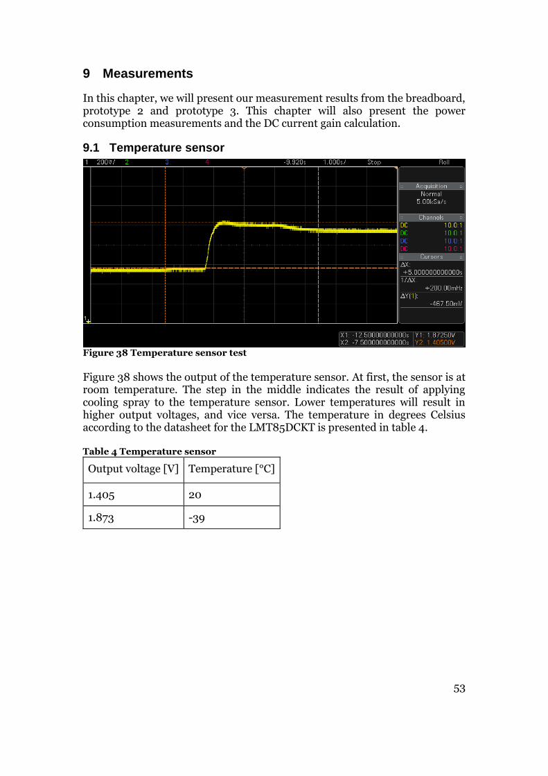
53
9 Measurements
In this chapter, we will present our measurement results from the breadboard, prototype 2 and prototype 3. This chapter will also present the power consumption measurements and the DC current gain calculation.
9.1 Temperature sensor
Figure 38 Temperature sensor test
Figure 38 shows the output of the temperature sensor. At first, the sensor is at room temperature. The step in the middle indicates the result of applying cooling spray to the temperature sensor. Lower temperatures will result in higher output voltages, and vice versa. The temperature in degrees Celsius according to the datasheet for the LMT85DCKT is presented in table 4. Table 4 Temperature sensor
Output voltage [V] Temperature [°C]
1.405 20
1.873 -39

54
9.2 System tests
All the results below was obtained using the Si BJT. We had not received the SiC BJT at the time for these tests.
Figure 39 Si measurement results. From DC sweep
The test in figure 39 was done on a breadboard. We used a signal generator to generate the Vin signal (yellow line). A saw-tooth signal was selected to emulate a DC Sweep. The signal was set to have a peak-to-peak voltage of 3.0 V and a frequency of 500 Hz. VCE was set to 3.3 V
The green line is the VRB1, blue is VBE and red is VRC.
Figure 40 Si measurement results. From pulse mode with slow filter
In figure 40 we built our circuit on a breadboard. We generated pulses from 0 V to 3.3 V with a frequency of 500 Hz on the input. VCE was set to 3.3 V. The breadboard contains the slow filter with:
𝐶𝐶 = 470 𝑝𝐹
𝐶𝐷 = 4700 𝑝𝐹 𝑅 = 4.02 𝑘𝛺

55
which gives a cut-off frequency of:
𝑓𝑑𝑖𝑓𝑓 = 4.0 𝑘𝐻𝑧
𝑓𝑐𝑚 = 84.0 𝑘𝐻𝑧
The green line is the VRB1, blue is VBE and red is VRC.
Figure 41 Si measurement results. From pulse mode with fast filter
In figure 41 we use a breadboard. We generated a pulse from 0 V to 3.3 V on the input. And used a frequency of 500 Hz. VCE is set to 3.3 V.
The breadboard contains the fast filter with:
𝐶𝐶 = 47 𝑝𝐹 𝐶𝐷 = 470 𝑝𝐹 𝑅 = 4.02 𝑘𝛺
which gives a cut-off frequency of:
𝑓𝑑𝑖𝑓𝑓 = 40 𝑘𝐻𝑧
𝑓𝑐𝑚 = 840 𝑘𝐻𝑧
The green line is the VRB1, blue is VBE and red is VRC.

56
Figure 42 Results from prototype 3
Figure 42 shows the outputs from prototype 3. The microcontroller uses USART (Universal Synchronous/Asynchronous Receiver/Transmitter) to send the data. The data can then be presented in a program that displays the data as graphs. This program was written by the microcontroller group using the Processing environment [6].
9.3 Power consumption
Figure 43 Power consumption Vcc
This test will only show the power consumption on the VCC. Keep in mind that there is also a VDD supply. However, the power consumption on VDD is very low in comparison to VCC. VDD only supplies the temperature sensor and the input to the op-amp that sets the collector-emitter voltage. The temperature sensor draws only between 5 µA and 10 µA. The op-amp only needs a bias current of 20 nA – 50 nA. This corresponds to a maximum power consumption of:
𝑃 = (10 µ𝐴 + 50 𝑛𝐴) ∗ 3.3 𝑉 = 33.2 µ𝑊 (9.1)

57
Therefore, we disregard the power consumption from VDD.
To measure the power consumption we added a resistor of 99.57 Ω in series with VCC. VCC was set to about 11 V to make sure that the supply voltage to the circuit was at least 10 V. We used saw-tooth input with 3.3 V peak-to-peak and frequency of 500 Hz. Figure 43 shows the voltage drop over the 99.57 Ω resistor. The result is also presented in Table 5. Table 5 Power consumption
Voltage [V] Current [mA] Power [mW]
Maximum 0.651 6.54 65.38
Minimum 0.108 1.08 10.85
9.4 DC current gain
We used prototype 2 together with a signal generator to perform a manual DC sweep. The purpose of this test was to measure the DC current gain of the BJT. The voltages across the base and collector resistors were measured in order to get their corresponding currents. The sweep went from 0.1 V to 3.3 V, with an inclination of 0.1 V per measurement point.

58
Figure 44 Gummel Log-Linear plot from manual DC sweep
Figure 45 Gummel Log-Log plot from manual DC sweep

59
10 Conclusions
During this project, we have evaluated different designs and components for a test circuit. The final design has been integrated together with the DC/DC-converter and the microcontroller. The experiment has then been implemented on a PCB. The test circuit has been proven to work together with the other parts of the SiC in Space project. It has also been proven to work independently. Our goal was to make a functional prototype of the experiment. This goal has been met since the experiment is working, as shown in the results although the experiment lacks a SiC BJT as of now. We were able to build the experiments only using COTS components. This is very fortunate since the circuit can be made much cheaper than if it had to be built using space graded components. The results that we got from the experiment showed that the DC current gain remained at around 100. This was unexpected. We expected, based on our simulations, that the DC current gain initially would be lower and then increase with the collector current. The constant DC current gain might have been caused by the small interval of currents that we used. The DC current gain might actually have changed, but was too small for us to measure. By using a larger interval of currents we might be able to receive measurement results that are more similar to the simulation results. It will take a while to get a PCB made by a professional manufacturer. This was something that we expected. To cope with the situation we used alternative methods as well. These methods included building the circuit on a breadboard and milling a PCB at KTH. However, you could get far by using simulations. One limiting factor was the lack of a SiC BJT. We have not been able to perform any test with it on a breadboard or PCB. The results we have obtained from the SiC BJT originates from simulations.
10.1 Future work
The method of measuring temperature has to be further investigated. We have neither been able to prove if it works nor if this is a preferable method. The circuit should be tested in different ambient temperatures to see how it will behave. This still needs to be done.
More work needs to be done regarding the EMC aspect. We need to measure how much EMI is generated and how much the MIST project tolerates. We also need to investigate how much interference our circuit can expect and whether the RFI-filters is needed or if the immunity needs to increase further.
The selection of the Si BJT needs to be reevaluated since the DC current gain was very constant. The first thing to test would be to use larger currents. We might have used a too small collector current to actually see any change in the DC current gain.

60
We have not calculated any measurement errors. The instrumental amplifiers have a voltage offset on the output and the resistors values changes with temperature. There are also a number of other parameters which affects our measurement error. Therefore, more work has to be done to determine how big the measurement errors are.

61

62
References
[1] “KTH | The Student Satellite MIST.” [Online]. Available:https://www.kth.se/en/sci/centra/rymdcenter/studentsatellit/studentsat elliten-mist-1.481707. [Accessed: 31-May-2016].
[2] S. May, “What Is Orbit?,” NASA, 01-Jun-2015. [Online]. Available: http://www.nasa.gov/audience/forstudents/5-8/features/nasa-knows/what-is-orbit-58.html. [Accessed: 08-Jun-2016].
[3] R. Hedayati, L. Lanni, A. Rusu, and C. M. Zetterling, “Wide Temperature Range Integrated Bandgap Voltage References in 4H-SiC,” IEEE Electron Device Lett., vol. 37, no. 2, pp. 146–149, Feb. 2016.
[4] O. Thorheim, S. D. Engineer, and D. Respons, “Electronics in space,” Data Respons, 10-Nov-2014. .
[5] M. M. R. Ahmed, N. A. Parker-Allotey, P. A. Mawby, M. Nawaz, and C. Zaring, “Characterization of the static and dynamic behavior of a SiC BJT,” in Power Electronics and Motion Control Conference, 2008. EPE-PEMC 2008. 13th, 2008, pp. 2472–2477.
[6] H. Paulsson and M. André, “Design of microcontroller circuit and measurement software for SiC and MOREBAC experiment,” KTH Information and Communication Technology, Stockholm, Bachelor’s Thesis TRITA-ICT-EX-2016:38, Jun. 2016.
[7] S. Johansson, “Design of power supplies for Sic and Piezo LEGS experiment,” KTH Information and Communication Technology, Stockholm, Bachelor Thesis TRITA-ICT-EX-2016:36, Jun. 2016.
[8] A. Berggren, “Design of Thermal Control System for the Spacecraft MIST,” KTH, Stockholm, 2015.
[9] S. Frankeser, S. Hiller, G. Wachsmuth, and J. Lutz, “Using the on-state-Vbe,sat-voltage for temperature estimation of SiC-BJTs during normal operation,” in Renewable Energy and Energy Management; Proceedings of PCIM Europe 2015; International Exhibition and Conference for Power Electronics, Intelligent Motion, 2015, pp. 1–8.
[10] C. Nagarajan, R. G. D’souza, S. Karumuri, and K. Kinger, “Design of a cubesat computer architecture using COTS hardware for terrestrial thermal imaging,” in 2014 IEEE International Conference on Aerospace Electronics and Remote Sensing Technology (ICARES), 2014, pp. 67–76.
[11] Y. Akisheva and R. Farid, “Radiation Dose Analysis of the MIST Satellite,” KTH.
[12] “Lesson(s) Learned: Space Radiation Effects on Electronic Components in Low-Earth Orbit.” [Online]. Available: http://llis.nasa.gov/lesson/824.[Accessed: 31-May-2016].
[13] D. Sinclair and J. Dyer, “Radiation Effects and COTS Parts in SmallSats,” Sinclair Interplanetary, Skybox Imaging, Toronto, Ontario, Canada,Mountain View, California, USA.
[14] S. Godard Desmarest, “Reliability of Pb-free solders for harsh environment electronic assemblies,” Mater. Sci. Technol., vol. 28:3.
[15] J. A. Brusse, G. J. Ewell, and J. P. Siplon, “Tin Whiskers: Attributes And Mitigation,” 2002. [Online]. Available:

63
http://nepp.nasa.gov/whisker/reference/tech_papers/brusse2002-paper-tin-whiskers-attributes-and-mitigation-CARTS-europe.pdf. [Accessed: 31-May-2016].
[16] M. Osterman, “Mitigation Strategies for Tin Whiskers,” 28-Aug-2002.[Online]. Available: http://www.calce.umd.edu/lead-free/tin-whiskers/TINWHISKERMITIGATION.pdf. [Accessed: 31-May-2016].
[17] Linear technology, “LTspice Getting Started Guide,”LTspiceGettingStartedGuide, 2011. [Online]. Available:http://cds.linear.com/docs/en/software-and-simulation/LTspiceGettingStartedGuide.pdf. [Accessed: 01-Jun-2016].
[18] “Solutions - LTspice.” [Online]. Available:http://www.linear.com/solutions/ltspice. [Accessed: 01-Jun-2016].
[19] “Simulation Models: MMBT2369AL.” [Online]. Available:http://www.onsemi.com/PowerSolutions/supportDoc.do?type=models&rpn=MMBT2369AL. [Accessed: 01-Jun-2016].
[20] “AD8226 Datasheet and Product Info | Analog Devices.” [Online].Available:http://www.analog.com/en/products/amplifiers/instrumentation-amplifiers/ad8226.html#product-overview. [Accessed: 01-Jun-2016].
[21] “Solving SPICE Convergence Problems,” http://www.intusoft.com/.[Online]. Available: http://www.intusoft.com/articles/converg.pdf.[Accessed: 01-Jun-2016].
[22] “Convergence problems? - LTwiki-Wiki for LTspice.” [Online].Available: http://ltwiki.org/?title=Convergence_problems%3F. [Accessed:01-Jun-2016].
[23] R. Hedayati, L. Lanni, A. Rusu, and C. M. Zetterling, “WideTemperature Range Integrated Bandgap Voltage References in 4H#x2013;SiC,” IEEE Electron Device Lett., vol. 37, no. 2, pp. 146–149, Feb.2016.

64
Appendix A Datasheets
Si BJT MMBT2369ALT1G http://www.onsemi.com/PowerSolutions/product.do?id=MMBT2369AL [Accessed: 08-Jun-2016]
Temperature sensor LMT85DCKT http://www.ti.com/product/LMT85 [Accessed: 08-Jun-2016]
Operational amplifier LT1638HS8 http://www.linear.com/product/LT1638 [Accessed: 08-Jun-2016]
Instrumental amplifier AD8226ARZ http://www.analog.com/en/products/amplifiers/instrumentation- amplifiers/ad8226.html#product-overview [Accessed: 08-Jun-2016]
MOSFET FDC637AN https://www.fairchildsemi.com/products/discretes/fets/mosfets/FDC637AN.html#status-price-package [Accessed: 08-Jun-2016]
22 kΩ, 100 kΩ, 6.8 kΩ, 15 kΩ, 82 Ω, 12 kΩ, 27 kΩ, 100 kΩ, 6.65 kΩ, 4.7 kΩ ERA3AEBxxxV http://industrial.panasonic.com/cdbs/www-data/pdf/RDA0000/AOA0000C237.pdf [Accessed: 08-Jun-2016]
510 Ω CPF0603B510RE1 http://www.te.com/usa-en/product-4-1676481-8.html#pdp-docs-features [Accessed: 08-Jun-2016]
4.02 kΩ CPF0603B4K02E1http://www.te.com/usa-en/product-1-1879224-3.html [Accessed: 08-Jun-2016]
300 Ω CPF0603B300RE1 http://www.te.com/usa-en/product-4-1676481-2.html [Accessed: 08-Jun-2016]
3.24 Ω ERJ3EKF3241V
http://industrial.panasonic.com/cdbs/www-data/pdf/RDA0000/AOA0000C86.pdf [Accessed: 08-Jun-2016]
0.1µF, 470pF, 4700pF, 0603NxxxJ500CT http://www.farnell.com/datasheets/1958513.pdf [Accessed: 08-Jun-2016]
1 µF C0603C105K4RACTU http://www.farnell.com/datasheets/1851736.pdf [Accessed: 08-Jun-2016]
47 pF MCMT18N470F250CT http://www.farnell.com/datasheets/1825496.pdf [Accessed: 08-Jun-2016]
Diode 1N4148WShttp://www.farnell.com/datasheets/1695880.pdf [Accessed: 08-Jun-2016]

65
Appendix B Simulation schematics
LTSpice Si BJT test circuit

66
LTSpice SiC BJT test circuit

67
Appendix C Prototypes
Prototype 1 Schematic

68
Prototype 1 PCB

69
Prototype 1 Bill of materials Name Description Type Comments
Diff_Rb_Si Instrumental amplifier AD8226ARZ
Diff_Rb_SiC Instrumental amplifier AD8226ARZ
Diff_Rc_Si Instrumental amplifier AD8226ARZ
Diff_Rc_SiC Instrumental amplifier AD8226ARZ
DUT_Si Silicon BJT MMBT2369alt11
DUT_SiC Produced at KTH
J1 Connector Input
J2 Connector Output
Op_Si Operational amplifier LT1638HS8
Op_SiC Operational amplifier LT1638HS8
Op_Ube Operational amplifier LT1638HS8
Q1 MOSFET FDC637AN
Q2 MOSFET FDC637AN
R1_Si Resistor 22 kΩ Amplification
R1_SiC Resistor 22 kΩ Amplification
R2_Si Resistor 10 kΩ Amplification
R2_SiC Resistor 10 kΩ Amplification
Rb1_Si Resistor 47 kΩ Base resistor 1, Si
Rb1-SiC Resistor 15 kΩ Base resistor 1, SiC
Rb2_Si Resistor 100 kΩ Base resistor 2, Si
Rb2_SiC Resistor 22 kΩ Base resistor 2, SiC
Rc_Si Resistor 300 Ω Collector resistor, Si
Rc_SiC Resistor 510 Ω Collector resistor, SiC
Rss1.1 Resistor 6.65 kΩ Sensor Supply
Rss1.2 Resistor 6.65 kΩ Sensor Supply
Rss2.1 Resistor 3.24 kΩ Sensor Supply
Rss2.2 Resistor 3.24 kΩ Sensor Supply
Temp_Si Temperature sensor LMT85DCKT
Temp_SiC Temperature sensor LMT85DCKT

70
Prototype 2 Schematic
71
Prototype 2 PCB Milled
72
Prototype 2 Bill of materials Name Description Type Comments
C1.1 Capacitor 47 pF/470 pF Fast/Slow, RFI-filter, CC
C1.2 Capacitor 470 pF/4700 pF Fast/Slow, RFI-filter, CD
C1.3 Capacitor 47 pF/470 pF Fast/Slow, RFI-filter, CC
C2.1 Capacitor 47 pF/470 pF Fast/Slow, RFI-filter, CC
C2.2 Capacitor 470 pF/4700 pF Fast/Slow, RFI-filter, CD
C2.3 Capacitor 47 pF/470 pF Fast/Slow, RFI-filter, CC
D1.1 Diode 1N4148 Voltage clamp
D1.2 Diode 1N4148 Voltage clamp
D2.1 Diode 1N4148 Voltage clamp
D2.2 Diode 1N4148 Voltage clamp
Diff1 Instrumental amplifier AD8226
Diff2 Instrumental amplifier AD8226
DUT Silicon BJT MMBT2369alt1 Device Under Test
J1 Connector Inputs
J2 Connector Outputs
Op1 Operational amplifier LT1638
Op2 Operational amplifier LT1638
Q1 MOSFET FDC637AN
R1 Resistor 10 kΩ Amplification
R2 Resistor 22 kΩ Amplification
R1.1 Resistor 4.02 kΩ RFI-filter
R1.2 Resistor 4.02 kΩ RFI-filter
R1.3 Resistor 10 kΩ Voltage clamp
R2.1 Resistor 4.02 kΩ RFI-filter
R2.2 Resistor 4.02 kΩ RFI-filter
R2.3 Resistor kΩ Voltage clamp
RB1 Resistor 47 kΩ Base resistor 1
RB2 Resistor 100 kΩ Base resistor 2
RC Resistor 300 Ω Collector resistor
Temp1 Temperature sensor LMT85DCKT
Temp2 Temperature sensor LMT85DCKT

73
Prototype 3 Schematic

74
Prototype 3 PCB Milled
75
Prototype 3 Bill of materials Name Description Type Comments
10K1 Resistor 10 kΩ DC/DC-converter
10uF Capacitor 10 μF DC/DC-converter
10uFu Capacitor 10 μF DC/DC-converter
1nF Capacitor 1 nF DC/DC-converter
47K Resistor 47 kΩ DC/DC-converter
750K Resistor 750 kΩ DC/DC-converter
B1 Button RESET MCU
C1 Capacitor 100 nF MCU
C2 Capacitor 0.1 μF Decoupling
C3 Capacitor 0.1 μF Decoupling
C4 Capacitor 0.1 μF Decoupling
C5 Capacitor 10 μF MCU
C6 Capacitor 10 μF MCU
C7 Capacitor 100 nF MCU
C8 Capacitor 100nF MCU
C10 Capacitor 100 nF MCU
C11 Capacitor 100 nF MCU
C12 Capacitor 1 μF MCU
C13 Capacitor 100 nF MCU
C1.1.1 Capacitor 47 pF RFI-filter
C1.1.2 Capacitor 470 pF RFI-filter
C1.1.3 Capacitor 47 pF RFI-filter
C1.1.4 Capacitor 1 μF Decoupling
C1.1.5 Capacitor 0.1 μF Decoupling
C1.2.1 Capacitor 47 pF RFI-filter
C1.2.2 Capacitor 470 pF RFI-filter
C1.2.3 Capacitor 47 pF RFI-filter
C1.2.4 Capacitor 1 μF Decoupling
C1.2.5 Capacitor 0.1 μF Decoupling
C2.1.1 Capacitor 47 pF RFI-filter
C2.1.2 Capacitor 470 pF RFI-filter
C2.1.3 Capacitor 47 pF RFI-filter
C2.1.4 Capacitor 1 μF Decoupling
C2.1.5 Capacitor 0.1μF Decoupling
C2.2.1 Capacitor 47 pF RFI-filter
C2.2.2 Capacitor 470 pF RFI-filter
C2.2.3 Capacitor 47 pF RFI-filter
C2.2.4 Capacitor 1 μF Decoupling
C2.2.5 Capacitor 0.1 μF Decoupling
DC_in MCU
Diff1.1 AD8226ARZ
Diff1.2 AD8226ARZ
Diff2.1 AD8226ARZ
Diff2.2 AD8226ARZ
F1 Fuse_1812 Fuse MCU
I2C 644456-3 Pin-header MCU
76
J5 SWD Pin-header MCU
L2 Ferrit 0805 220 MCU
MMBT2369ALT1G Si BJT DUT
Op1 Operational amplifier LT1638HS8
Op2 Operational amplifier LT1638HS9
OpUbe Operational amplifier LT1638HS10 Error not connected
OpUbe0 Operational amplifier LT1638HS11 Error not connected
Q1 MOSFET FDC637AN
Q2 MOSFET FDC637AN
R6 Resistor 10 k MCU
R7 Resistor 0 Ω MCU
R.2.2 Resistor 22 kΩ Amplification
R1.1 Resistor 10 kΩ Amplification
R1.2 Resistor 22 kΩ Amplification
R1.1.1 Resistor 4.02 kΩ RFI-filter
R1.1.2 Resistor 4.02 kΩ RFI-filter
R1.1.3 Resistor 10 kΩ RFI-filter
R1.2.1 Resistor 4.02 kΩ RFI-filter
R1.2.2 Resistor 4.02 kΩ RFI-filter
R1.2.3 Resistor 10 kΩ RFI-filter
R2.1 Resistor 10 kΩ Amplification
R2.1.1 Resistor 4.02 kΩ RFI-filter
R2.1.2 Resistor 4.02 kΩ RFI-filter
R2.1.3 Resistor 10 kΩ RFI-filter
R2.2.1 Resistor 4.02kΩ RFI-filter
R2.2.2 Resistor 4.02kΩ RFI-filter
R2.2.3 Resistor 10 kΩ RFI-filter
RB1.1 Resistor 47 kΩ Base resistor 1
RB1.2 Resistor 100 kΩ Base resistor 2
RB2.1 Resistor 15 kΩ Base resistor 1
RB2.2 Resistor 22 kΩ Base resistor 2
RC1 Resistor 300 Ω Collector resistor
RC2 Resistor 510 Ω Collector resistor
SiCBJT SiC BJT DUT
Temp1 LMT85DCKT Temperature sensor
Temp2 LMT85DCKT Temperature sensor
U1 3062 MCU
U2 MCU, LQFP48 STM32L053C MCU
U7 LM1117 3.3 V MCU
USART 644456-4 Pin-header MCU
Vin 644456-2 Pin-header MCU

77

TRITA TRITA-ICT-EX-2016:37
www.kth.se