design, implementation, modeling, and optimization of … · design, implementation, modeling, and...
TRANSCRIPT
Design, Implementation, Modeling, and Optimization of Next Generation Low-Voltage
Power MOSFETs
by
Abraham Yoo
A thesis submitted in conformity with the requirements for the degree of Doctor of Philosophy
Department of Materials Science and Engineering University of Toronto
© Copyright by Abraham Yoo 2010
ii
Design, Implementation, Modeling, and Optimization of Next
Generation Low-Voltage Power MOSFETs
Abraham Yoo
Doctor of Philosophy
Department of Materials Science and Engineering
University of Toronto
2010
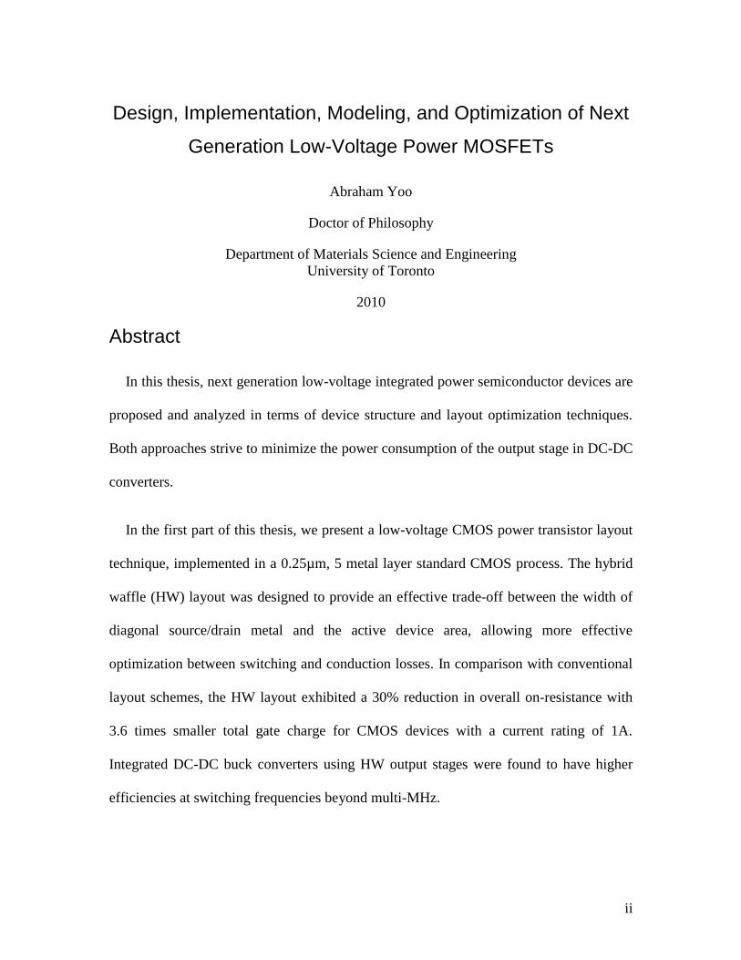
Abstract
In this thesis, next generation low-voltage integrated power semiconductor devices are
proposed and analyzed in terms of device structure and layout optimization techniques.
Both approaches strive to minimize the power consumption of the output stage in DC-DC
converters.
In the first part of this thesis, we present a low-voltage CMOS power transistor layout
technique, implemented in a 0.25µm, 5 metal layer standard CMOS process. The hybrid
waffle (HW) layout was designed to provide an effective trade-off between the width of
diagonal source/drain metal and the active device area, allowing more effective
optimization between switching and conduction losses. In comparison with conventional
layout schemes, the HW layout exhibited a 30% reduction in overall on-resistance with
3.6 times smaller total gate charge for CMOS devices with a current rating of 1A.
Integrated DC-DC buck converters using HW output stages were found to have higher
efficiencies at switching frequencies beyond multi-MHz.

iii
In the second part of the thesis, we present a CMOS-compatible lateral superjunction
FINFET (SJ-FINFET) on a SOI platform. One drawback associated with low-voltage SJ
devices is that the on-resistance is not only strongly dependent on the drift doping
concentration but also on the channel resistance as well. To resolve the issue, a SJ-
FINFET structure consisting of a 3D trench gate and SJ drift region was developed to
minimize both channel and drift resistances. Several prototype devices were fabricated in
a 0.5µm CMOS compatible process with nine masking layers. In comparison with
conventional SJ-LDMOSFETs, the fabricated SJ-FINFETs demonstrated approximately
30% improvement in Ron,sp. This is a positive indication that the SJ-FINFET can become
a competitive power device for sub-100V rating applications.

iv
Acknowledgements
First of all, I would like to thank Prof. Wai Tung Ng for his supervision,
encouragement, and invaluable counsel throughout my Ph.D. program. Without whose
presence my development as both a student and an individual would not have progressed
as rapidly. I wish to further acknowledge Prof. Johnny Sin (Hong Kong University of
Science and Technology) and Yasuhiko Onishi (Visiting Scientist from Fuji Electric
Corp.) who have contributed to my knowledge in the field, which better enabled me to
carry out and finish my research project on time.
I would like to express appreciation to all the members in the Smart Power Integration
& Semiconductor Devices Research Group for their fruitful discussions over the course
of this research, particularly M. Chang, O. Trescases, H. Wang, E. Xu, G. Wei, and Q.
Fung. I would also like to express my appreciation to all the staff in Nanoelectronic
Fabrication Facility (NFF) at HKUST who provided me with various IC fabrication
support.
Financial support from the University of Toronto Open Fellowship, the Natural
Sciences and Engineering Research Council of Canada, and the Auto21 Network of
Centres of Excellence of Canada are gratefully acknowledged.
Lastly, I would like to extend my appreciation to my wife, Mia Yoo for her patience,
consideration and support during the past four years. She has been wonderful and a true
partner. Also, special thanks to my mother and parents-in-law for their constant support
and encouragement throughout the studies.

v
Table of Contents
Table of Contents .............................................................................................................. v
List of Tables .................................................................................................................. viii
List of Figures ................................................................................................................... ix
List of Glossary .............................................................................................................. xiv
List of Symbols ............................................................................................................... xvi
Chapter 1 Introduction ..................................................................................................... 1
1.1 Technology and Market Trends in Power Semiconductors ...................................... 1
1.2 Advantages of Power MOSFET Devices ................................................................. 3
1.3 Application Fields for Current and Future Power MOSFETs .................................. 4
1.4 Thesis Objectives and Organization ......................................................................... 6
Chapter 2 Power MOSFETs – a Brief Overview ........................................................... 7
2.1 Fundamentals of MOS Device .................................................................................. 7
2.2 Types of Power MOSFETs ..................................................................................... 11
2.2.1 Traditional Vertical Power MOSFETs ............................................................ 12
2.2.2 Traditional Lateral Power MOSFETs .............................................................. 14
2.3 CMOS-based Power MOSFETs ............................................................................. 18
2.3.1 Monolithic Integration: Standard CMOS Process ........................................... 18
2.3.2 CMOS Layout Techniques for Power Integrated Circuits ............................... 20
2.4 Super-Junction (SJ) Power MOSFETs ................................................................... 25
2.4.1 Device Concept and Characteristics ................................................................ 25
2.4.2 Current Status and Challenges of SJ Power MOSFETs .................................. 27
Chapter 3 Analytical Layout Modeling of Power MOSFET ...................................... 30
3.1 Analysis of Basic MOS Finger Structure................................................................ 30
3.2 Modeling of Conventional Multi-Finger (MF) Layout ........................................... 33

vi
3.3 Modeling of Regular Waffle (RW) Layout ............................................................ 36
3.4 Proposed Hybrid Waffle (HW) Layout ................................................................... 38
3.4.1 Lfinger-Optimization of HW Layout Structure .................................................. 40
3.4.2 Performance Evaluation via FOM ................................................................... 42
3.4.3 Simulated Characteristics of Different Layout Structures ............................... 48
3.5 Summary ................................................................................................................. 53
Chapter 4 High Speed CMOS Output Stage for Integrated DC-DC Converter ...... 54
4.1 Output Stage Design based on 5V Hybrid Waffle Layout ..................................... 55
4.1.1 Design of Low-Side Switch: N-channel MOSFETs ........................................ 56
4.1.2 Design of High-Side Switch: P-channel MOSFETs ........................................ 59
4.1.3 Power Connection Routings ............................................................................ 61
4.1.4 ESD Protection, Power Clamp, and Guard Rings ............................................ 62
4.2 IC Fabrication and Packaging ................................................................................. 66
4.3 Test PCB Design ..................................................................................................... 68
4.4 Experimental Results and Discussion ..................................................................... 70
4.4.1 On-Resistance Measurements .......................................................................... 70
4.4.2 Gate-drive Loss Measurements ........................................................................ 75
4.4.3 Efficiency Measurements ................................................................................. 77
4.5 Summary ................................................................................................................. 79
Chapter 5 Device Structure and Analysis of the SJ-FINFET on SOI ........................ 80
5.1 Device Structure and Operating Concept ............................................................... 81
5.2 Process Simulations ................................................................................................ 87
5.2.1 Simulation of P-body Formation ..................................................................... 87
5.2.2 Simulation of SJ-drift Formation ..................................................................... 89
5.2.3 Simulation of N+ Source/Drain Contact Formation ........................................ 91
5.3 Device Simulations ................................................................................................. 92
5.3.1 Mesh Structure and Grid Refinement .............................................................. 92
5.3.2 Off-State Simulations ....................................................................................... 94
5.3.3 On-State Simulations ....................................................................................... 99

vii
5.4 Comparison with Conventional SJ-LDMOS and Si Limit ................................... 103
5.4.1 Specific On-Resistance and Mobility Profiles ............................................... 103
5.4.2 Electric Field Distribution .............................................................................. 105
5.4.3 Trade-off Relationship between Ron,sp and BV .............................................. 108
5.5 Summary ............................................................................................................... 109
Chapter 6 Device Fabrication and Characterization of the SJ-FINFET on SOI .... 110
6.1 Process Design Considerations ............................................................................. 110
6.2 SJ-FINFET in a 0.5µm Standard CMOS Process Flow ........................................ 116
6.3 Layout, Mask and Test Structures ........................................................................ 127
6.4 Experimental Results and Discussion ................................................................... 132
6.4.1 Transfer Characteristics ................................................................................. 133
6.4.2 Output Characteristics .................................................................................... 134
6.4.3 Specific On-Resistance for Different N/P Pillar Width Ratio ....................... 136
6.4.4 Breakdown Voltage for Different SJ-drift Regions ....................................... 137
6.4.5 Comparison with Fabricated SJ-LDMOSFETs ............................................. 138
6.5 Summary ............................................................................................................... 141
Chapter 7 Conclusions .................................................................................................. 142
References: ..................................................................................................................... 144
APPENDIX-I: Calculation Methods of Parasitic Resistors ...................................... 154
APPENDIX-II: Parameter Extractions for Power MOSFETs ................................. 157
APPENDIX-III: Process Flow of SJ-FINFET ............................................................ 160
List of Publication ......................................................................................................... 167

viii
List of Tables
Table 3.1 Data for different NN matrix of RW layout structures .................................. 36
Table 3.2 Data for different NN matrix of HW layout structures .................................. 38
Table 3.3 Parameter Summary of Trench-Gate Power MOSFETs ................................... 42
Table 3.4 Parameter Summary of Lateral-Diffusion Power MOSFETs ........................... 42
Table 3.5 Efficiency Simulation Conditions: Conventional Power MOSFETs ............... 43
Table 3.6 Parameter Summary of CMOS-based Power MOSFETs ................................. 44
Table 3.7 Efficiency Simulation Conditions: CMOS-based Power MOSFETs ............... 44
Table 3.8 Simulation Data Summary of MF, RW, and HW Layout Structures ............... 52
Table 4.1 Target Specification .......................................................................................... 54
Table 4.2 Summary of 5V power MOSFETs with Hybrid Waffle Layout Structure ....... 55
Table 4.3 Package Description of the Integrated HW Output Stage ................................ 67
Table 4.4 Summary of on-resistance measurements......................................................... 71
Table 4.5 Data comparison between simulated and measured on-resistances. ................. 75
Table 4.6 Summary of Gate-Drive Power Calculated from Measurements ..................... 76
Table 5.1: Parameters considered for both process and device simulations ..................... 86
Table 6.1 Parameters and specifications of the SOI wafer used in the fabrication ........ 111
Table 6.2 Summary of SJ-FINFET process parameters ................................................. 126
Table 6.3 Summary of SJ-FINFET layout design rules .................................................. 128
Table 6.4 SJ-FINFET Mask Information ........................................................................ 129

ix
List of Figures
Fig. 1.1 Evolution of power semiconductors. ..................................................................... 2
Fig. 1.2 Annual estimate and forecast of worldwide power semiconductor market........... 3
Fig. 1.3 Power device technologies and applications with respect to their voltages and
current ratings. ....................................................................................................... 5
Fig. 2.1 Basic Structure of a MOS transistor (n-type MOSFET) ....................................... 9
Fig. 2.2 An equivalent circuit for n-type MOSFET showing the parasitic capacitances and
resistances. ............................................................................................................. 9
Fig. 2.3 Types of Power Semiconductor Devices ............................................................. 11
Fig. 2.4 Structure of V-MOSFET. .................................................................................... 12
Fig. 2.5 Structure of DMOSFET....................................................................................... 13
Fig. 2.6 Structure of UMOSFET....................................................................................... 14
Fig. 2.7 Basic Structure of LDMOSFET .......................................................................... 15
Fig. 2.8 A RESURF LDMOSFET structure at full depletion ........................................... 17
Fig. 2.9 Functional elements of smart power technology ................................................. 18
Fig. 2.10 A conventional multi-finger (MF) layout structure ........................................... 21
Fig. 2.11 A modified version of MF layout structure with wider metal layers ................ 22
Fig. 2.12 A conventional Regular Waffle (RW) layout structure ..................................... 22
Fig. 2.13 Cross-section of a SJ-DMOSFET...................................................................... 26
Fig. 2.14 Ron,sp versus BV for different power device technologies [62-70]. ................... 29
Fig. 3.1 A basic MOS finger layout with simple interconnect resistive components. ...... 30
Fig. 3.2 (a) Two different MOS finger layouts with min. and max. metal-1 widths, ....... 31
Fig. 3.3 (a) Ron and (b) Ron,sp vs. Wtotal for different numbers of MOS fingers. ............... 32
Fig. 3.4 Conventional MF layout structure with parasitic resistors. ................................. 33
Fig. 3.5 A MF NMOS layout (10 MOS fingers) structure with minimum design rules. .. 35
Fig. 3.6 Corresponding schematic resistance model of the MF NMOS layout. ............... 35
Fig. 3.7 Schematic of (a) 44 regular waffle layout and (b) the corresponding resistance
model. .................................................................................................................. 37
Fig. 3.8 Hybrid waffle structure: (a) a layout and (b) a corresponding resistance model. 39
Fig. 3.9 Simulated Ron and Qg data for different Lfinger values of HW layouts. ................ 40

x
Fig. 3.10 FOM-1 & FOM-2 versus different Lfinger of HW layout structures. .................. 41
Fig. 3.11 FOM vs. Efficiency for conventional power MOSFETs. .................................. 43
Fig. 3.12 Efficiency vs. Conventional FOM for CMOS-based Power MOSFETs. .......... 45
Fig. 3.13 Cross-sectional views of Trench-gate, LDMOS, and CMOS power MOSFETs.
............................................................................................................................ 45
Fig. 3.14 Efficiency vs. New FOM for CMOS-based Power MOSFETs. ........................ 48
Fig. 3.15 Gate charge characteristics of (a) MF and (b) HW layout structures ................ 49
Fig. 3.16 RON and QG plots as a function of MF, RF and HW layout active areas. .......... 50
Fig. 3.17 Comparison of power conversion efficiencies for both MF and HW layout
structures as a function of switching frequency and for different load currents:51
Fig. 4.1 Power MOSFET Output Stage: (a) Layout and (b) Schematic ........................... 55
Fig. 4.2 HW_NMOS unit-cell: (a) Active, (b) M1, (c) M2, (d) M3, (e) M4, and (f) M5. 56
Fig. 4.3 HW_NMOS unit-cell: (a) Layout and (b) Schematic (w/o parasitics) ................ 57
Fig. 4.4 Gate Segmentations of NMOS array: (a) layout and (b) schematic. ................... 58
Fig. 4.5 Layout comparison between segments: (a) Gate_N<6> and (b) Gate_N<0>. .... 58
Fig. 4.6 HW_PMOS unit-cell: (a) Active, (b) M1, (c) M2, (d) M3, (e) M4, and (f) M5 . 59
Fig. 4.7 Gate Segmentations of PMOS array: (a) layout and (b) schematic. .................... 60
Fig. 4.8 Layout comparison between segments: (a) Gate_P<0> and (b) Gate_P<6>. ..... 60
Fig. 4.9 Power Connection Routing Layouts: (a) M1-M3 and (b) M4-M5 layers. .......... 61
Fig. 4.10 Metal stress relief pattern on a routing metal wire. ........................................... 61
Fig. 4.11 2kV HBM and 400 MM ESD protection circuit, (a) layout (b) schematic. ...... 62
Fig. 4.12 ESD Protection Circuit Under Input Pad: (a) layout and (b) schematic. ........... 63
Fig. 4.13 Power Clamp, esd_nclamp5v_ 500p4U, (a) layout and (b) schematic. ............ 64
Fig. 4.14 p-type high resistance poly-resistor, rphripoly, (a) layout and (b) schematic. .. 65
Fig. 4.15 Seal and guard ring layout. ................................................................................ 65
Fig. 4.16 A micrograph of an integrated output stage using Hybrid Waffle layout in
TSMC 0.25µm standard CMOS technology...................................................... 66
Fig. 4.17 A micrograph of source/drain metal runners (M3-M5). .................................... 67
Fig. 4.18 A micrograph of the packaged HW chip. .......................................................... 68
Fig. 4.19 a) System Overview and b) X-ray Image of QFN-12 package. ........................ 68
Fig. 4.20 Test PCB: (a) layout (silkscreen-view) and (b) photograph. ............................. 69

xi
Fig. 4.21 Test circuits for on-resistance measurements: (a) NMOS and (b) PMOS ........ 70
Fig. 4.22 Measured on-resistance vs. # of segments at different voltage ratings. ............ 73
Fig. 4.23 Comparison between simulated and measured on-resistances: ......................... 74
Fig. 4.24 Total dynamic and gate-drive power measurements. ........................................ 76
Fig. 4.25 Measured power conversion efficiency of HW output stage with a test
conditions: fs = 6.25MHz, Vin = 2.7V, Vout = 1.8V, L = 2.2 µH, and C = 100nF.
............................................................................................................................ 77
Fig. 4.26 10MHz switching characteristic at Iout = 158mA. ............................................. 78
Fig. 4.27 Measured power conversion efficiency of HW segmented output stage at
10MHz switching frequency: Vin = 3.6V, Vout = 1.8V, L = 1µH, and C = 56nF.
............................................................................................................................ 78
Fig. 5.1 Basic idea of SJ-FINFET structure: (a) a fin-gate and (b) with a SJ-drift region 81
Fig. 5.2 (a) Overview of the proposed lateral SJ-FINFET structure and (b) Schematic
cross-sections along the cut-lines: A-A‟ and B-B‟ .............................................. 83
Fig. 5.3 Ideal device structure of the proposed SJ-FINFET. ............................................ 85
Fig. 5.4 P-body formation of the SJ-FINFET: (a) a trench formation by reactive ion
etching process, (b) after 45° tilted B+ ion implantation and thermal annealing
process, (c) a doping concentration profile along X-cut line at X=2, and (d) a
doping concentration profile along Y-cut at Y=-3. ............................................. 88
Fig. 5.5 P-pillar formation of the SJ-FINFET structure: (a)-(d) are the cross-sections
along the B-B‟ cut line after 12° tilted B+ ion implantation (left) and thermal
diffusion (right) steps and (e)-(h) are the corresponding doping profiles for
different B+ ion implantation doses. .................................................................... 90
Fig. 5.6 N+ source/drain contact formation of the SJ-FINFET: (a) after 45° tilted dual-
implant of n-type dopant species (i.e. arsenic and phosphorus) and thermal
diffusion steps, and (b) a doping concentration profile along Y-cut line at Y=-3.
............................................................................................................................. 91
Fig. 5.7 Unit-cell of the SJ-FINFET: a) w/ and b) w/o any oxide materials .................... 93
Fig. 5.8 Contour plots of the electrostatic potential distribution in off-state for a proposed
SJ-FINFET with p-pillar impurity concentration of 9.25 x 10¹⁶
cm3
under charge
balance: a) w/ and b) w/o any oxide materials ................................................... 96

xii
Fig. 5.9 Contour plots of the electric field distribution in off-state for a proposed SJ-
FINFET with p-pillar impurity concentration of 9.25 x 10¹⁶
cm3
under charge
balance: a) w/ and b) w/o refined mesh structure. .............................................. 97
Fig. 5.10 The relationship between BV and charge imbalance for the proposed SJ-
FINFET with Ldrift of 3.0 µm and 6.0 µm, Wn = Wp = 0.3 µm and trench depths
(Wside) of 2.0 µm and 3.0 µm. ............................................................................ 98
Fig. 5.11 I-V characteristics of the proposed SJ-FINFETs during off-state for various drift
region lengths. .................................................................................................... 98
Fig. 5.12 Transfer characteristics of the SJ-FINFET with Ldrift = 3.5 µm. ....................... 99
Fig. 5.13 On-state simulations: (a) electron current density distribution and (b) output
characteristics of the SJ-FINFET with Ldrift =4.5 µm and device area = 1 mm2.
.......................................................................................................................... 101
Fig. 5.14 I-V characteristics of the proposed SJ-FINFETs during on-state for various drift
region lengths. .................................................................................................. 102
Fig. 5.15 The trade-off relationship between BV and Ron,sp of the SJ-FINFET for different
drift region lengths. .......................................................................................... 102
Fig. 5.16 Specific on-resistance profile along C-C‟ cut line during on-state for
conventional SJ SOI-LDMOS and the proposed SJ-FINFETs ........................ 104
Fig. 5.17 Mobility profile along C-C‟ cut line during on-state for conventional SJ SOI-
LDMOS and the proposed SJ-FINFET with Wside = 3 µm. ............................. 105
Fig. 5.18 Comparison of the electric field distribution (along the C-C‟ cut line) for the SJ-
FINFETs with two different values of NA at ND= 7.4 × 10¹⁶
cm3
and Wside = 2
µm. ................................................................................................................... 106
Fig. 5.19 Electric field distribution comparison between the conventional SJ-LDMOS and
SJ-FINFETs at NA = 9.25 × 10¹⁶
cm3
and ND = 7.4 × 10¹⁶
cm3
. ................... 107
Fig. 5.20 Performance comparison between SJ simulation results with different trench
gate depths and previously published data. ...................................................... 108
Fig. 6.1 Standard CMOS process flow with additional steps for the lateral SJ-FINFET
implementation. ................................................................................................. 112
Fig. 6.2 Six sequential processing steps required for the deep trench isolation region. . 113
Fig. 6.3 Process Flow of the SJ-FINFET (Part 1 of 5) ................................................... 121

xiii
Fig. 6.4 Layout design rules for the proposed SJ-FINFET device on a SOI platform. .. 127
Fig. 6.5 A full test chip layout of both SJ-FINFET and SJ-LDMOS device. ................. 131
Fig. 6.6 Some of the process structures: (a) critical dimensions and (b)-(c) alignment
marks. ................................................................................................................ 131
Fig. 6.7 Micrograph of the fabricated test integrated chip (Optical: × 200). .................. 132
Fig. 6.8 Top-view of SJ-FINFET device: (a) a layout and (b) a corresponding fabricated
structures. .......................................................................................................... 133
Fig. 6.9 SEM images of fabricated SJ-FINFET: (a) a transistor array and (b) a cross-
section after Al and oxide etchings. .................................................................. 133
Fig. 6.10 Ids - Vgs transfer characteristic of the fabricated SJ-FINFET at Vgs = 0.1 V. .. 134
Fig. 6.11Output I-V characteristics of the fabricated (a) SJ-LDMOSFET and (b) SJ-
FINFET devices, Ldrift = 3.5 µm and Wtotal = 200 µm. .................................... 135
Fig. 6.12 The specific on-resistance of the fabricated SJ-FINFETs for different n/p pillar
width ratios and SJ-drift trench (DTI) widths. ................................................. 136
Fig. 6.13 The relationship between BV and P-pillar dose for the fabricated SJ-FINFET
devices with Ldrift of 3.5 µm and 6 µm, Wn = Wp = 0.3 µm and Wside of 2.7 µm.
.......................................................................................................................... 137
Fig. 6.14 On-resistance data comparison as a function of the gate width (W) of the
fabricated SJ-FINFET and SJ-LDMOSFETS, Ldrift = 3.5 µm. ........................ 138
Fig. 6.15 Ron,sp data comparison between SJ-FINFET and SJ-LDMOS for different Ldrift.
.......................................................................................................................... 139
Fig. 6.16 Micrographs of the SJ-FINFETs with different drift lengths: (a) Ldrift = 3.5 µm,
(b) Ldrift = 6.0 µm, (c) ) Ldrift = 10.0 µm and (d) ) Ldrift = 12.0 µm for Wtotal = 200
µm. ................................................................................................................... 139
Fig. 6.17 Performance comparison between the fabricated SJ-devices and previously
published data. Data from [102], [104], [114] are for conventional
LDMOSFETs. Data from [103], [111-113] are for conventional SJ-
LDMOSFETs. .................................................................................................. 140

xiv
List of Glossary
ASIC: Application Specific Integrated Circuits
ASSP: Application-Specific Standard Products
BJT: Bipolar Junction Transistor
BV: Breakdown Voltage
BOX: Buried Oxide Layer (SOI Wafer)
CAGR: Cumulative Average Growth Rate
CMOS: Complementary Metal Oxide Semiconductor
CMP: Chemical Mechanical Polishing
DMOS: Double Diffused MOS
DTI: Deep Trench Isolation
ESD: Electro-Static Discharge
FET: Field Effect Transistor
FOM: Figure of Merit
FINFET: Fin-Field Effect Transistor
GTO: Gate Turn-off Thyristor
HW: Hybrid-Waffle (Layout Style)
HS: High-Side (Output Switch)
HBM: Human Body Model (ESD)
IGBT: Insulated Gate Bipolar Transistor
ICP-RIE: Induced Coupled Plasma RIE
LDMOSFET: Lateral Double-Diffused MOSFET
LS: Low-Side (Output Switch)

xv
LOCOS: LOCal Oxidation of Silicon
LTO: Low Temperature Oxide
MOS: Metal Oxide Semiconductor
MF: Multi-Finger (Layout Style)
MM: Machine Model (ESD)
PIC: Power Integrated Circuits
PECVD: Plasma Enhanced CVD
QFN: Quad Flat No-Lead (Package Type)
RESURF: Reduced SURface Field
RIE: Reactive Ion Etching
RW: Regular-Waffle (Layout Style)
SOA: Safe Operation Area
SEG: Selective Epitaxial Growth
SAD: Substrate-Assisted Depletion
SJ: Super-Junction
SOI: Silicon-On-Insulator
SFB: Silicon Fusion Bonded (SOI Wafer)
STI: Shallow Trench Isolation

xvi
List of Symbols
Cgd: Gate to Drain Capacitance, or Miller Capacitance
Cgs: Gate to Source Capacitance
Ciss: Input Capacitance
Coss: Output Capacitance
Crss: Reverse Transfer Capacitance
si : Dielectric Constant of Silicon (=1.03×10⁻¹²
F/cm)
ox : Dielectric Constant of Oxide (=3.45×10⁻¹²
F/cm)
Ec: Critical Electric Field
fs: Converter Switching Frequency
Lg: Gate or Channel Length
Ldrift: Drift Length
NA: Acceptor or Hole Doping Concentration
ND: Donor or Electron Doping Concentration
in : Intrinsic Carrier Concentration
Pcond: Conduction Power Loss
Pdyn: Dynamic Power Loss
Pgate: Gate-Drive Power Loss
Psw: Switching Power Loss
q : Electronic Charge (=1.60×10⁻¹⁹
C)
Qg: Total Gate Charge
Qgs: Gate to Source Charge

xvii
Qgd: Gate to Drain Charge
Rg: Gate Resistance
Ron: On-Resistance
Ron,sp: Specific On-Resistance (Ron × Area)
Rp: Project Range of Implant
Sn or Sp: Cross-sectional Area of n-drift or p-drift region
Tox: Oxide Thickness or Gate Oxide Thickness
Tepi: Epi. Thickness (SOI Wafer)
on : Turn-On Delay
off : Turn-Off Delay
ch : Carrier Mobility in the Channel
Vth: Threshold Voltage
Vin: Input Supply Voltage
Vout: Output Voltage
Vgate: Gate Voltage
Vgs: Gate to Source Voltage
Vds: Drain to Source Voltage
Wg: Gate or Channel Width
Wd: Depletion Width
Wn or Wp: n-pillar or p-pillar Width
Wside: Trench Gate Depth
Wtop: Top Gate Width
Wtotal: Total Channel Width

1
Chapter 1 Introduction
Over the last decade, there has been a growing research interest in the area of high-
efficient power integrated circuits (PICs) for various electronic applications. Especially
portable electronics products, such as cell phones, laptops, MP3 players, PDAs, digital
cameras, and other compact battery powered products have gained tremendous popularity
in the market place during the last few years. Power management ICs play a critical role
in these systems to offer a long battery operating time and many power-saving features at
the same time. The most important and largest device block in power management IC is
the output power stage, which can switch or regulate large amounts of power using many
parallel-connected power transistors. MOS power transistors have several advantages
over their bipolar counterparts, including a majority carrier device, simpler drive
requirements, and lower forward voltages. These advantages make MOS transistors
extremely useful power devices [1-4]. In this chapter, power device technology, market
trends, advantages/disadvantages, their current and future applications, and the objectives
of this thesis will be addressed.
1.1 Technology and Market Trends in Power Semiconductors
The growth of today‟s power electronics has been centering on AC-DC inverters and
DC-DC converters as the key system topologies. This has been accelerated by several
evolutionary changes and breakthroughs in the areas of power semiconductor device and
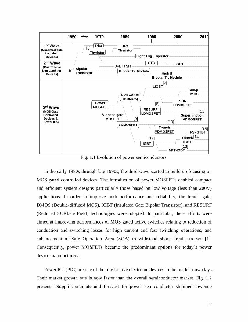
process technologies. Fig. 1.1 shows the historical growth of power semiconductor
devices. In the 1960s, the introduction of the thyristor generated the first wave in the
history of power semiconductor devices and opened up many possibilities for the growth
of power electronics as a whole. In the second half of the 1970s, the bipolar transistor
module and the gate turn-off thyristor (GTO) were introduced for the growing demand of
power conversion equipment and they quickly became the focus of power electronics
growth. This started the second wave in the chronological evolution of power
semiconductor devices [5].
2
Fig. 1.1 Evolution of power semiconductors.
In the early 1980s through late 1990s, the third wave started to build up focusing on
MOS-gated controlled devices. The introduction of power MOSFETs enabled compact
and efficient system designs particularly those based on low voltage (less than 200V)
applications. In order to improve both performance and reliability, the trench gate,
DMOS (Double-diffused MOS), IGBT (Insulated Gate Bipolar Transistor), and RESURF
(Reduced SURface Field) technologies were adopted. In particular, these efforts were
aimed at improving performances of MOS gated active switches relating to reduction of
conduction and switching losses for high current and fast switching operations, and
enhancement of Safe Operation Area (SOA) to withstand short circuit stresses [1].
Consequently, power MOSFETs became the predominant options for today‟s power
device manufacturers.
Power ICs (PIC) are one of the most active electronic devices in the market nowadays.
Their market growth rate is now faster than the overall semiconductor market. Fig. 1.2
presents iSuppli‟s estimate and forecast for power semiconductor shipment revenue
1950 1970 1980 1990 2000 2010∼1950 1970 1980 1990 2000 2010∼1st Wave
(Uncontrollable
Latching
Devices)
2nd Wave(Controllable
Non-Latching
Devices)
3rd Wave(MOS-Gate
Controlled
Devices &
Power ICs)
Triac
Bipolar
Transistor
RC
ThyristorThyristor
GTO
Light Trig. Thyristor
JFET / SIT
Bipolar Tr. ModuleHigh β
Bipolar Tr. Module
GCT
RESURF
LDMOSFET
IGBT
NPT-IGBT
Trench
VDMOSFET
Trench
IGBT
FS-IGTBT
Superjunction
VDMOSFET
LDMOSFET
(EDMOS)SOI-
LDMOSFET
Sub-µ
CMOS
V-shape gate
MOSFET
VDMOSFET
Power
MOSFET
LIGBT[7]
[8]
[9][10]
[11]
[12]
[13]
[14]
[15]
[6]

3
during the period from 2006 to 2011 [16]. The power semiconductor market is expected
to increase at a cumulative average growth rate (CAGR) of 8% per year to $15.5 billion
in 2011. Among several different power device technologies, the switching regulator,
power management ASIC/ASSP (Application-Specific Integrated Circuits or Standard
Products), and low voltage power MOSFET applications are currently contributing more
than half of total market revenue. Especially, the switching regulator and low voltage
power MOSFETs are used in almost all portable electronics and automotive components.
In recent years, with the rising output of whole systems, these two products are
developing relatively faster than the others as demonstrated in this figure.
Fig. 1.2 Annual estimate and forecast of worldwide power semiconductor market.
1.2 Advantages of Power MOSFET Devices
In general, bipolar transistors are not suitable for high speed switching applications
because they saturate when their collector-base junctions is forward-biased. Saturation
greatly increases the amount of minority carrier charges stored in both the neutral base
and collector. A transistor cannot turn-off until these stored charges recombine or diffuse
across a junction. A typical power bipolar transistor therefore exhibits a saturation delay
of about a microsecond. This delay effectively places an upper limit on switching speeds
LV LV LV
LV LV
LV
SWR SWR SWR SWR SWR SWR
$16B

4
of about 500 kHz [3]. On the other hand, MOS transistors are majority carrier devices.
They do not exhibit any saturation delay, thus they can switch at speed in excess of multi
MHz [3]. Another advantage of power MOSFETs are their simple drive circuitry. The
average current through the gate drive of a typical one-amp power MOSFET is only a
few milliamps. Bipolar transistors generally require much higher drive currents due to a
low current gain ().
Power MOSFETs can also conduct large currents at very low drain-to-source
voltages. The behavior of a MOS transistor under these conditions can be derived from
the Shichman-Hodges theory for the linear region [17]. The simplified theory reveals a
linear relationship between the drain-to-source voltage and the drain current. The
transistor behaves as if it is a resistor whose value is known as the on-resistance. The on-
resistance can be reduced to arbitrarily small values by increasing the W/L ratio.
However, in practice, considerations such as die size, cost, metallization resistance, and
bond-wire resistance place practical limitation upon the on-resistance. In general, the
limitations are more severe in low voltage power MOSFETs (<100V) because they
require more precise circuit topologies and interconnections. Hence, there are many on-
going research projects to overcome those limitations at device design/fabrication, circuit
design, wafer, and package levels.
1.3 Application Fields for Current and Future Power MOSFETs
Power MOSFETs are ideally suited for use in many electronic applications, such as
automotive circuits, motor and solenoid drives, inverters in electronic ballast, consumer
appliances, telecommunications, display drivers, switching power suppliers, factory
automation, etc. as illustrated in Fig. 1.3. The applications for power semiconductor
technology stretch over a very wide range of power levels. The voltage and current
handling needs for both device technologies and applications are summarized in this
diagram. For many portable applications, the DC-DC converters are popular for
conversion of battery power to an appropriate DC output voltage [18-19]. Another fast
growing application field is the automotive industry; particularly in hybrid, electric, and

5
fuel cell vehicles. Low voltage power MOSFETs (<100V) are widely used in engine
control, vehicle dynamic control, vehicle safety, and body electronics subsystems in both
electric and conventional internal combustion engine vehicles [20-21].
Fig. 1.3 Power device technologies and applications with respect to their voltages and
current ratings.
Although silicon devices have dominated power electronics, the performance limit of
silicon as a semiconductor material is starting to become a serious issue. This implies that
new materials are needed to satisfy the future requirements of high performance power
devices. Wide band gap semiconductors, such as SiC [22-25] and GaN [26-31], recently
gained much attention as novel power devices with certain advantages over silicon in
terms of higher critical field, mobility and operating temperature. However several issues
including process, reliability, interconnection and packaging need to be solved before
these new materials will enjoy a reasonable market share. Therefore, despite the
limitations of silicon as a semiconductor material, it still has plenty of thrust until the
wide band gap materials become popular.
GTO
HVIC
DMOST/IGBT
Linear IC
Bipolar
Thyristor
IGBTPower
SupplyBattery
control
Smart PIC
(BCD)
Motor
Control
DC/DC converterAutomation
Electronics
Factory
Automation
Triac
HVDCAD/DC
converter
Motor
Control
Lamp
Ballast
Telecom
Circuits
Display
Driver
Digital IC
CMOS
1 10 100 1000 100000.0
01
0.0
10.1
110
100
1000
Device Blocking Voltage Rating (V)
Devic
e C
urr
ent
Rating (
A)
GTO
HVIC
DMOST/IGBT
HVIC
DMOST/IGBT
Linear IC
Bipolar
Linear IC
Bipolar
Thyristor
IGBTPower
SupplyBattery
control
Battery
control
Smart PIC
(BCD)
Smart PIC
(BCD)
Motor
Control
Motor
Control
DC/DC converterDC/DC converterAutomation
Electronics
Automation
Electronics
Factory
Automation
Factory
Automation
Triac
HVDCAD/DC
converter
AD/DC
converter
Motor
Control
Motor
Control
Lamp
Ballast
Lamp
Ballast
Telecom
Circuits
Display
Driver
Digital IC
CMOS
1 10 100 1000 100000.0
01
0.0
10.1
110
100
1000
Device Blocking Voltage Rating (V)
Devic
e C
urr
ent
Rating (
A)

6
1.4 Thesis Objectives and Organization
The objectives of the thesis are to design, implement, and optimize the next
generation of low-voltage silicon power MOSFETs. New device structure and layout
optimization techniques are proposed and analyzed for sub-100V applications. Both
approaches strive to minimize the power consumption of the output stage in DC-DC
converters.
Chapter 2 describes the state of the art of power semiconductor devices. It provides a
review of the recent developments in vertical and lateral power semiconductor
technologies. Also, it discusses the fundamental device physics concerning power
semiconductors, several of the important physical models for both circuit and device
simulations, and some of the related topics including layout techniques and super-
junction concept.
In Chapter 3, the analytical layout modeling of three different layout structures is
presented. Specific attention is given to a new layout strategy named “Hybrid Waffle”
structure. Layout optimization and performance evaluation via simulations are also given.
In Chapter 4, experimental work such as the integrated circuit implementation on a DC-
DC converter, test circuit board design, and various electrical measurements are
presented for verification purposes.
In Chapter 5, a novel device structure that is suitable for practical implementation of
lateral superjunction FINFET (SJ-FINFET) is proposed, simulated and compared with
other conventional power MOSFETs. Both process and device simulation studies are
presented to extract and validate the specific processing conditions and the optimal
device characteristics, respectively. In Chapter 6, the performance advantage of the SJ-
FINFET over the conventional SJ-LDMOSFET is verified experimentally. Detailed
fabrication process scheme is presented followed by various electrical measurement
results of the devices.
Finally, in Chapter 7, conclusions and suggestions for future work are discussed.

7
Chapter 2 Power MOSFETs – a Brief Overview
2.1 Fundamentals of MOS Device
Metal-oxide-semiconductor (MOS) is a major class of integrated circuits. MOS
technology is used in microprocessors, microcontrollers, static RAM, and other digital
logic circuits. Also, it is used for a wide variety of analog circuits such as image sensors,
data converters, and highly integrated transceivers for many types of applications [3].
Two important characteristics of the Complementary MOS (CMOS) technology are high
noise immunity and low static power consumption. Significant power is only drawn when
the transistors are switching between on and off states. Consequently, MOS circuitry
dissipates less power and is denser than other implementations having the same
functionality. As this advantage has grown and become more important, the vast majority
of modern integrated circuit manufacturing is on CMOS processes.
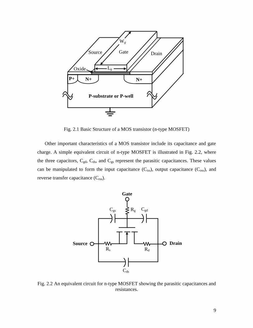
The basic structure of MOS transistor (i.e. n-type MOSFET) is shown in Fig. 2.1,
where n+ represents heavily doped n-type silicon with low resistivity. The difference
between the source and drain is that the source n+ is shorted to the p-substrate by the
source metal. This is important for fixing the potential of the p-substrate for normal
device operation. For power device applications, the MOSFET is necessary to be off
when the voltage on the gate is zero. The turn-on of the MOSFET relies on the formation
of a conductive channel on the surface of the semiconductor, when a positive (or
negative) voltage is applied on the gate of the n-type (or p-type) MOSFET. For the n-type
MOSFET, as Vg increases, electrons gather at the interface between the oxide and silicon,
and a charged layer is formed to provide a "channel" for the current. When this
phenomenon occurs, the value of Vg is called the threshold voltage (Vth). In
semiconductor physics, the Vth is defined as the applied gate voltage required to make the
surface of the silicon strongly inverted (i.e. as n-type in terms of carrier concentration as
the p-type substrate. The threshold voltage can be written as [32]:

8
m s
ox
ssdep
fpthC
QQV
2 (Eq.2.1)
where i
afp
n
N
q
kTln (Eq.2.2)
afpsidep NqQ 4 (Eq.2.3)
ox
oxox
TC
(Eq.2.4)
The definitions of the other symbols are:
1)` k is the Boltzmann's constant: k =1.38×10⁻²³
J/K,
2)`T is the absolute temperature,
3)` q is the electronic charge: q =1.60×10⁻¹⁹
C,
4)` aN is the acceptor doping concentration of the substrate,
5)` in is the intrinsic carrier concentration of the silicon,
6)` si is the dielectric constant of silicon: si =1.03×10⁻¹²
F/cm,
7)` ssQ is the fixed charge located in the oxide close to the oxide-silicon interface,
8)` ox is the dielectric constant of oxide: ox =3.45×10⁻¹²
F/cm, and
9)` oxT is the thickness of the gate oxide.
The resistance from drain to source of the MOSFET is determined by the property of
the charged layer in the channel, and can be expressed as [32]:
)( thgsoxchg
oxg
chVVW
TLR
(Eq.2.5)
where nch is the carrier mobility in the channel. The definition of gL (gate length) and
gW (gate width) are shown in Fig. 2.1.
9
Fig. 2.1 Basic Structure of a MOS transistor (n-type MOSFET)
Other important characteristics of a MOS transistor include its capacitance and gate
charge. A simple equivalent circuit of n-type MOSFET is illustrated in Fig. 2.2, where
the three capacitors, Cgd, Cds, and Cgs represent the parasitic capacitances. These values
can be manipulated to form the input capacitance (Ciss), output capacitance (Coss), and
reverse transfer capacitance (Crss).
Fig. 2.2 An equivalent circuit for n-type MOSFET showing the parasitic capacitances and
resistances.
Gate
Source Drain
Cgs Cgd
Cds
Rg
Rs Rd
N+ N+
Lg
P+
P-substrate or P-well
Drain Source Gate
Oxide
Wg

10
Among these capacitors, the gate-drain capacitance Cgd, known as a Miller
capacitance is the most important parameter because it provides a feedback loop between
the device‟s output and its input. The switching behavior of the MOSFET is also
governed by the charging and discharging of the input capacitance which is the sum of
the gate-to-source capacitance (Cgs) and the gate-to-drain capacitance (Cgd). The gate
resistance (Rg) is also important because the switching delay is directly proportional to a
product of the distributed gate resistance and its capacitance.
However, the nonlinearity of the parasitic capacitances and the incomplete data on
their variation over the full range of relevant voltages, make a gate circuit by
conventional methods exceedingly difficult. To overcome this problem, it has become
standard practice to specify the total gate charge, Qg that has to be supplied in order to
establish a particular drain current under given test conditions. Data sheets from most
manufacturers normally divide the Qg into that required to charge the gate-to-source
capacitance, Qgs, and that required to supply the gate-to-drain capacitance, Qgd. The merit
of the gate charge parameter is that it is relatively insensitive to the drain current and the
precise circuit conditions used, and it is quite independent of temperature [1]. It allows a
very simple design methodology for obtaining the desired switching time, and it enables
the total charge and the total energy required to be easily estimated. The resulting average
current and power needed from the gate circuit can be also obtained throughout a
multiplication of the operating frequency.
Another important parameter of a MOS transistor is the breakdown voltage. It is the
reverse biased voltage in which a substrate-drain (or body-drift) diode breaks down and
significant current starts to flow between the source and drain by the avalanche
multiplication process. For drain voltages below the rated avalanche voltage and with no
bias on the gate, the drain voltage is entirely supported by the reverse biased p-n junction.
With a poor MOSFET design and process, punch-through breakdown can be observed
when the depletion region from the drain (or drift) junction reaches the source region at
drain voltages below the avalanche voltage. This also provides a current path between
source and drain and causes a soft breakdown characteristic.

11
2.2 Types of Power MOSFETs
The simple MOS structure was initially not suitable for discrete power ICs, because
in order to achieve the low channel resistance, shorter channel length ( gL ) and thinner
gate oxide ( oxT ) were mandatory. Since both gL and oxT are related to the breakdown
voltage of the MOS device, the MOS structure is not considered for the choice of power
devices, especially in medium and high voltage power ICs. For instance, if gL is too
small, the punch-through of n+pn
+ (or p
+np
+) of N-type (or P-type) MOSFET will occur;
if oxT is too thin, the oxide directly adjacent to the drain can be damaged or destroyed by
the electric field. To alleviate the effect of the electrical field on the gate oxide, several
traditional power MOS device structures have been developed and commercialized, as
illustrated in Fig. 2.3. In terms of a device structure, the power MOSFET family can be
divided into two different categories: lateral and vertical power MOSFETs.
Fig. 2.3 Types of Power Semiconductor Devices
Power Semiconductor Devices
CMOS LDMOS RESURF
2-terminal devices
Schottky diodePiN diode Power MOSFET
3-terminal devices
JFET IGBT BJT Thyristor
Lateral Vertical
UMOS V-MOS DMOS Cool MOS
Traditional Power MOSFETs
Minority carrier devices
Majority carrier devicesPower Semiconductor Devices
CMOS LDMOS RESURF
2-terminal devices
Schottky diodePiN diode Power MOSFET
3-terminal devices
JFET IGBT BJT Thyristor
Lateral Vertical
UMOS V-MOS DMOS Cool MOS
Traditional Power MOSFETs
Minority carrier devices
Majority carrier devices
12
Some well known examples of vertical power MOSFETs include V-MOS (V-shaped
MOS), DMOS (Double-diffusion MOS), UMOS (U-shaped MOS), and Cool MOS™
(Vertical Super-junction MOS from Infineon Technologies). The common lateral power
devices include LDMOS (Lateral Double-diffused MOS), RESURF (Reduced SURface
Field) LDMOS and CMOS power transistors. In the following sections, both traditional
vertical and lateral power MOSFETs are briefly discussed in terms of their intrinsic
structures and associated operating principles.
2.2.1 Traditional Vertical Power MOSFETs
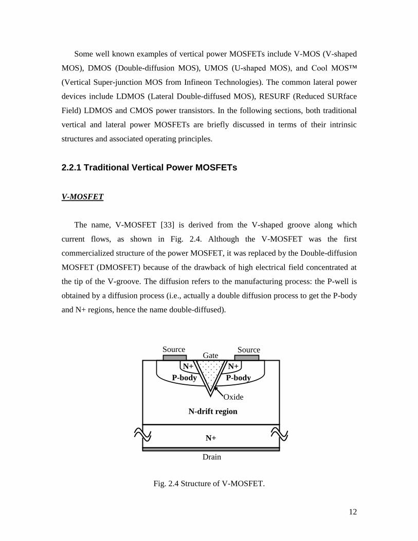
V-MOSFET
The name, V-MOSFET [33] is derived from the V-shaped groove along which
current flows, as shown in Fig. 2.4. Although the V-MOSFET was the first
commercialized structure of the power MOSFET, it was replaced by the Double-diffusion
MOSFET (DMOSFET) because of the drawback of high electrical field concentrated at
the tip of the V-groove. The diffusion refers to the manufacturing process: the P-well is
obtained by a diffusion process (i.e., actually a double diffusion process to get the P-body
and N+ regions, hence the name double-diffused).
Fig. 2.4 Structure of V-MOSFET.
Gate Source Source
P-body
N+ N+
P-body
N-drift region
N+
Drain
Oxide

13
DMOSFET
In Fig. 2.5, the cross-sectional vertical structure of the DMOSFET [33] is illustrated.
When Vg is higher than the threshold voltage and Vds is positive, the electron current of
the DMOSFET travels horizontally through the channel and then vertically down to the
drain. A more direct and shorter current path can be achieved if the channel is orientated
vertically instead of along the silicon surface. This idea is realized later by the structure
of the UMOSFET.
Fig. 2.5 Structure of DMOSFET.
UMOSFET
Similar to V-MOSFET, the UMOSFET is named from the U-shaped groove formed
in the gate region, as shown Fig. 2.6. In comparison with the DMOSFET structure, the
UMOSFET has no JFET effect, which is caused by the depletion of the region between
wells in the DMOSFET. The UMOSFET has higher channel density to significantly
reduce the on-resistance and also it has no sharp oxide tip (as in the V-MOSFET). This is
because that the corners of the gate oxide located in the n-drift region can be rounded by
isotropic etching. In order to prevent the catastrophic destruction of the gate oxide due to
the high electrical field at the corner of the trench, the p-body is usually designed to be
Source Source Gate Oxide
N+ N+
P-body P-body
N-drift region
Drain
N+

14
relatively deep. Also, the doping concentration at the bottom of the p-body is high
enough to ensure that the breakdown voltage occurs first at the junction of the p-body and
the n-drift region. As a result, the voltage can be clamped to save the gate oxide [34].
Fig. 2.6 Structure of UMOSFET.
2.2.2 Traditional Lateral Power MOSFETs
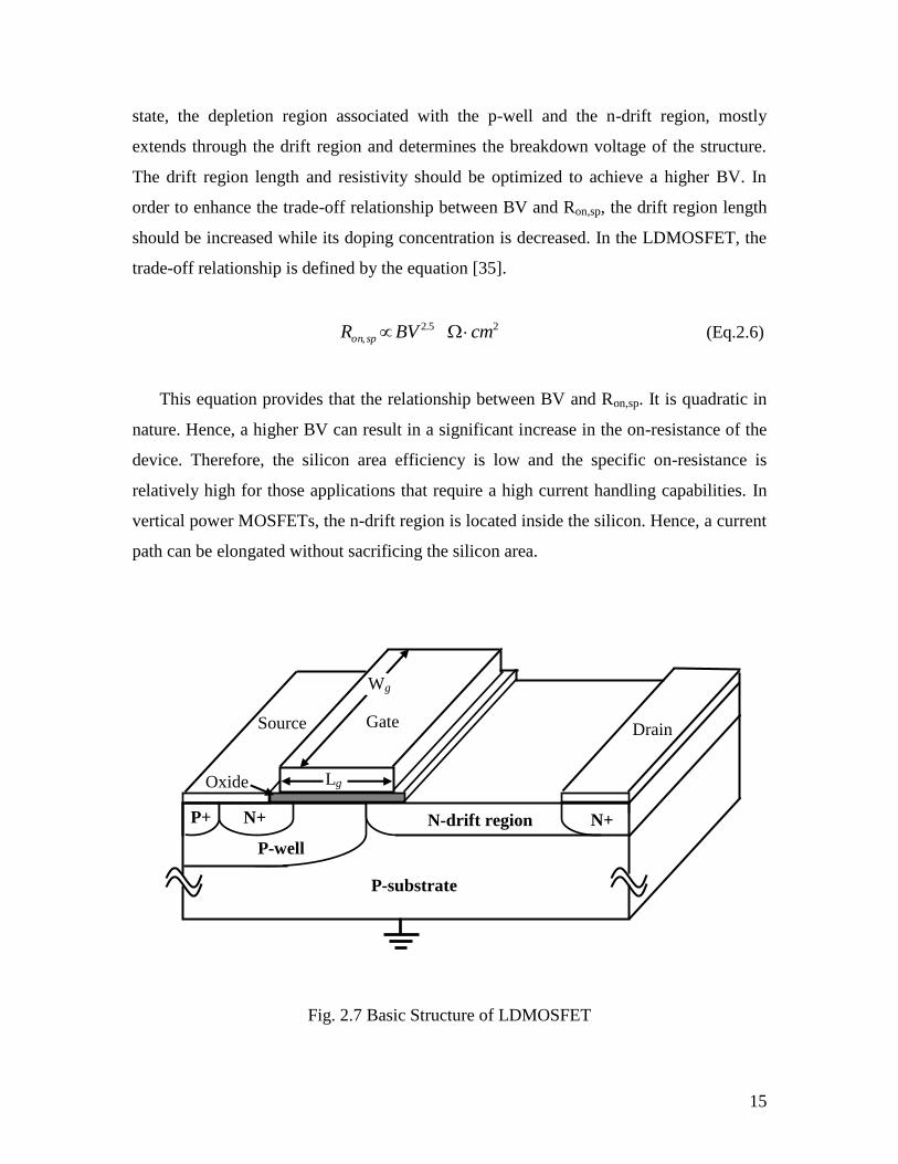
Lateral Double Diffused MOSFET (LDMOSFET)
The lateral double diffused MOSFET is the predominant power device in the
implementation of PICs because of many attractive electrical characteristics such as high
input impedance, low on-resistance, high breakdown voltage and fast switching speed. A
typical LDMOSFET structure is as illustrated in Fig. 2.7. In this structure, the current
flows laterally on the surface from the source to the drain electrode and the channel
region is implemented using double implantation of the p-well and the n+ source regions
through the same opening window. One of the main advantages in the LDMOSFET is
that it can be easily integrated into a standard CMOS process. In the on-state, when a
positive voltage, higher than the threshold voltage is applied to the gate, a conductive
channel forms at the surface of the p-well and electrons flow from the n+ source through
the highly conductive channel and the n-drift layer to the n+ drain electrode. In the off-
Drain
Source Source
N-drift region
N+
Source Gate Gate
Oxide
N+ N+ N+ N+
P-body P-body P-body
15
state, the depletion region associated with the p-well and the n-drift region, mostly
extends through the drift region and determines the breakdown voltage of the structure.
The drift region length and resistivity should be optimized to achieve a higher BV. In
order to enhance the trade-off relationship between BV and Ron,sp, the drift region length
should be increased while its doping concentration is decreased. In the LDMOSFET, the
trade-off relationship is defined by the equation [35].
25.2, cmBVR spon (Eq.2.6)
This equation provides that the relationship between BV and Ron,sp. It is quadratic in
nature. Hence, a higher BV can result in a significant increase in the on-resistance of the
device. Therefore, the silicon area efficiency is low and the specific on-resistance is
relatively high for those applications that require a high current handling capabilities. In
vertical power MOSFETs, the n-drift region is located inside the silicon. Hence, a current
path can be elongated without sacrificing the silicon area.
Fig. 2.7 Basic Structure of LDMOSFET
N+ N+
Lg
P+
P-substrate
Drain Source Gate
Oxide
Wg
N-drift region
P-well

16
RESURF(Reduced SURface Field) LDMOSFET
In 1979, Appels and Vaes suggested the RESURF concept [36], which allows
significant improvement in the voltage blocking capability of lateral device. The cross
section of a RESURF LDMOSFET is as shown in Fig. 2.8. There are two different diodes
shown with the associated junctions such as a lateral junction at the n-drift/p-well
boundary and a vertical junction at the n-drift/p-substrate boundary. At an optimum
thickness and concentration of the n-drift layer, the depletion layer from both horizontal
and vertical n/p junctions allows the electric field at the surface to be lower than the
critical electric field. A higher breakdown occurs at the junction between the p-substrate
and n-drift layer when the electric field reaches the critical value, Ec.
Under the conditions, the thickness of the epitaxial layer, te must equal to the
depletion width, Wd in that layer as defined by the following equation [36].
se
sed
NNq
BVtW
(
)(2 (Eq.2.7)
where εs denotes the dielectric constant of silicon, q is the electronic charge, and Ne and
Ns are the doping concentration in the epitaxial layer and the substrate respectively. The
corresponding parallel plane breakdown voltage is then given by [36].
)(2
2
se
Cs
NNq
EBV
(Eq.2.8)
where Ec is the critical electric field in silicon. The charge density, Ne te in the epitaxial
layer is given by [36].
q
EtN C
see (Eq.2.9)

17
If Ne >> Ns, (Eq. 2.21) can be simplified to
2121021 cmtN ee (Eq.2.10)
A well designed silicon RESURF device, satisfying the above condition, can withstand
approximately 15 V/µm of drift region length.
The RESURF structure allows the optimized performance at high voltages in the off-
state, because the n-drift layer is fully depleted of charge carriers and the surface field is
reduced to a value of less than the critical electric field. The surface electric field profile
is uniform and has a flat shape at the surface. In the past decades, the RESURF
technology has been successfully commercialized for many lateral power semiconductor
devices such as diodes and LDMOS transistors for 20 – 1200V [37]. Although the
maximum blocking voltage of the RESURF LDMOSFET is greater than the conventional
LDMOSFET, this increase is limited to a few hundred volts because the lightly doped
epitaxial drift layer causes an increase in the on-resistance of the device.
Fig. 2.8 A RESURF LDMOSFET structure at full depletion
N+ P+
N-drift region
N+
P-well
P-substrate
te
E
Y
Ec
Gate
X
E Es < Ec

18
2.3 CMOS-based Power MOSFETs
The majority of today‟s VLSI chips are implemented with deep submicron CMOS
technologies. Therefore, the integration of other types of power MOSFETs into the
design requires additional fabrication process and time. In the following sections, the
monolithic integration of output power transistors and the associated layout techniques,
based on a standard CMOS technology is briefly discussed.
2.3.1 Monolithic Integration: Standard CMOS Process
Monolithic integration of output power semiconductors with digital and analog
circuitry includes power devices, signal processing, sensing, and protection circuits on
the same chip, as illustrated in Fig. 2.9. Monolithic solutions for power conversion and
amplification are highly desirable not only for the reduction of volume, weight and
electromagnetic interferences, but also for increasing efficiency, performance and
reliability of the overall system. A wide range of applications is predictable for these
monolithic solutions, since the power delivered by a power IC into a load can be several
to hundreds of watts. Many approaches are being investigated to search for new strategies
to reduce the cost and size of PICs [38-43].
Fig. 2.9 Functional elements of smart power technology
Smart Power ICs
Power Devices Control CircuitsSensing &
ProtectionInterface
IGBT
LDMOS
VDMOS
SJ-MOS
Bi-CMOS
CMOS
HV Level Shifter
Gate Drive Circuit
Analog Circuits
Over Temperature
Over Current
Under Voltage
Over Voltage
Logic Circuits
CMOS LSI

19
Monolithic integration is aimed at performing complex switching functions at high
frequencies, motivating progress in this area, and pushing manufacturers to launch
application-specific PICs into the market, especially for low-voltage power applications.
The impact of smart power technology on the recent advances in telecommunication and
automobile industries is remarkable because the drastic cost and size reductions are
possible by applying these monolithic solutions. For examples, a significant performance
gain and cost reduction can be easily achieved by implementing a standard CMOS or
CMOS-compatible processes to build up all necessary blocks required in smart power ICs.
Previous smart power devices have always used design rules and technologies which
are less efficient than that used for CMOS devices. In the early 80‟s, the first smart power
devices were fabricated with 2.5 or 4µm design rules while CMOS used 1µm design
rules. When CMOS devices used submicron IC design rules, smart power devices were
fabricated with 1 or 2µm design rules [5]. This difference was essentially linked (i) to the
more complex fabrication that must be taken into account: isolation, edge terminations
for power devices and combination of different kinds of devices, and (ii) to the rapid
development of CMOS devices driven by larger market forces. Recently, the design rules
for smart power devices went down to 0.35-0.13µm, which offers a greater possibility of
integrated CMOS-based power ICs. This strong drive towards integration leads to a
single chip system for low voltage power applications. Some manufacturers prefer a
mixed technology (e.g. Bi-CMOS); however, overall design rules do not help to reduce
the device area, because most of the chip size is determined by the on-chip power devices.
Since low voltage power MOSFETs implemented in a deep submicron CMOS process
exhibit much shorter switching delays than those in conventional power MOSFETs, this
allows the CMOS devices to operate in the MHz range for high-efficient mobile
applications. Nevertheless, one of the drawbacks is that more advanced CMOS
technology is accompanied with larger parasitic interconnect resistances and capacitances.
Without any processing and device structural changes, performance improvement can be
only gained by introducing a new layout structure. In the next section, several different
layout techniques for CMOS power device applications will be discussed in detail.

20
2.3.2 CMOS Layout Techniques for Power Integrated Circuits
As the switching frequency of power converters continues to increase, both switching
and gate-drive power losses start to limit the efficiency of output power stage.
Particularly, conventional vertical power MOSFETs have relatively large gate to drain
overlap area. This introduces a significant switching delay (τ = RC) since a large input
capacitance requires more charging and discharging time for each turn on and off
transition of a power MOSFET. On the other hand, CMOS-based power MOSFETs have
much smaller input gate capacitance due to smaller gate-drain/source overlap capacitance,
gate oxide capacitance and parasitic fringing capacitance. Therefore, CMOS power
MOSFETs have been the best choice for mobile SMPS applications operating in the
multi-MHz range. However, the distributed parasitic resistance associated with metal
interconnects to the source and drain terminals strongly affect the total on-resistance of a
large CMOS device (with a high W/L ratio). The previous research by Kayayama et.al
[18] demonstrated that simple power device models, which do not consider the effects of
metal resistance, can produce more than 50% variation in the Ron simulation for large
power MOS devices. The impact of the parasitic resistance is extremely dependent upon
the layout style of the power MOSFETs and the positioning of external source/drain
connections. Many efforts [41-44] have been made in the past to optimize the CMOS
layout to provide minimum parasitic resistance and capacitance. Some examples are
summarized in the following sections.
Multi-Finger (MF) Layout Structure
The multi-finger (MF) CMOS layout structure has been widely used in almost all
smart PICs. In general, MOS transistor with large device widths are needed to achieve
low channel resistance, and to maximize the operating frequency, the minimum gate or
channel length is used. To reduce the distributed gate resistance, a common layout
practice is to decompose it into many parallel transistors of smaller widths. This
conventional layout technique is known as a multi-finger distribution, as shown Fig. 2.10.
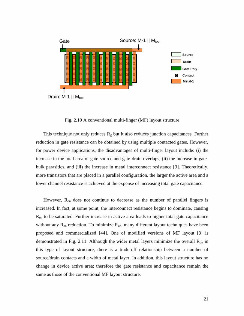
21
Fig. 2.10 A conventional multi-finger (MF) layout structure
This technique not only reduces Rg but it also reduces junction capacitances. Further
reduction in gate resistance can be obtained by using multiple contacted gates. However,
for power device applications, the disadvantages of multi-finger layout include: (i) the
increase in the total area of gate-source and gate-drain overlaps, (ii) the increase in gate-
bulk parasitics, and (iii) the increase in metal interconnect resistance [3]. Theoretically,
more transistors that are placed in a parallel configuration, the larger the active area and a
lower channel resistance is achieved at the expense of increasing total gate capacitance.
However, Ron does not continue to decrease as the number of parallel fingers is
increased. In fact, at some point, the interconnect resistance begins to dominate, causing
Ron to be saturated. Further increase in active area leads to higher total gate capacitance
without any Ron reduction. To minimize Ron, many different layout techniques have been
proposed and commercialized [44]. One of modified versions of MF layout [3] is
demonstrated in Fig. 2.11. Although the wider metal layers minimize the overall Ron in
this type of layout structure, there is a trade-off relationship between a number of
source/drain contacts and a width of metal layer. In addition, this layout structure has no
change in device active area; therefore the gate resistance and capacitance remain the
same as those of the conventional MF layout structure.
Gate
Drain: M-1 || Mtop
Source: M-1 || Mtop
Source
Drain
Gate Poly
Contact
Metal-1
22
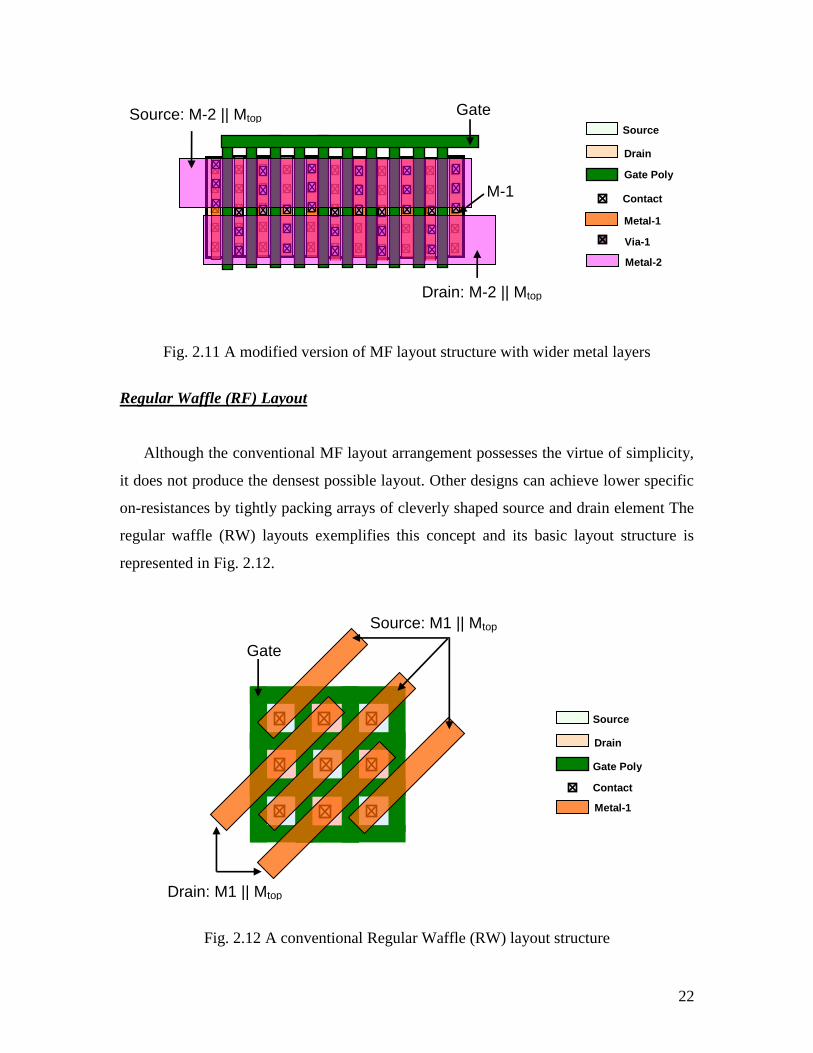
Fig. 2.11 A modified version of MF layout structure with wider metal layers
Regular Waffle (RF) Layout
Although the conventional MF layout arrangement possesses the virtue of simplicity,
it does not produce the densest possible layout. Other designs can achieve lower specific
on-resistances by tightly packing arrays of cleverly shaped source and drain element The
regular waffle (RW) layouts exemplifies this concept and its basic layout structure is
represented in Fig. 2.12.
Fig. 2.12 A conventional Regular Waffle (RW) layout structure
Gate Source: M-2 || Mtop
Drain: M-2 || Mtop
M-1
Source
Drain
Gate Poly
Contact
Metal-1
Via-1
Metal-2
Drain: M1 || Mtop
Source: M1 || Mtop
Gate
Source
Drain
Gate Poly
Contact
Metal-1

23
The RW layout uses a mesh of horizontal and vertical poly gate stripes to divide the
source/drain implant into an array of squares. Each square contains a single contact. By
alternately connecting these contacts to the source and drain metallization, one can
arrange four drains around each source and four sources around each drain [44]. The
drain and source metallization consists of a series of diagonal stripes of metal-1 and
upper parallel metal layers as shown in this figure.
An analysis of the W/L ratios achieved for a given device area shows that the waffle
layout structure provides an increase in packing density equal to [3]:
gategate
gate
MF
RW
SL
S
LW
LW
2
)/(
)/( (Eq.2.11)
where RWLW )/( of the waffle layout and MFLW )/( of the conventional multi-finger
layout are measured from two devices consuming equal die areas.
The RW layout offers a better packing density than the MF layout as long as the
spacing between the gates, gateS exceeds the gate length, gateL . Almost all power
MOSFET layout structures meet this requirement. For example, the layout rules specify a
minimum drawn gate length of 2µm, a minimum contact width of 1µm, and a minimum
spacing poly-to-contact of 1.5µm. Using these rules, Eq.2.11 indicates that the waffle
transistor provides approximately 33% higher transconductance than the conventional
multi-finger transistor. By allowing the source/drain area to be shared by more poly-
silicon gates, the waffle layout minimizes the active area, leading to smaller junction
capacitance. A small parasitic capacitance has not only a beneficial effect on the speed
requirement, but also on the power consumption of the chip, which is one of the key
issues in integrated design nowadays. In addition, the characteristic (i.e. compactness) of
the waffle layout leads to the reduction of thermal noise because the gate resistance is
also decreased.

24
However, the waffle-type transistor has three crucial deficiencies. First, due to the
restriction of minimum CMOS design rules (e.g. minimum metal width and spacing) of
the first metallization level, the source/drain diffusion area should be larger than the
minimum dimension to accommodate the metal lines connecting the source/drain regions
through the contacts. The metallization invariably contributes a significant portion of the
Ron of the transistor, and in more recent CMOS process technology nodes, it often
becomes the dominant factor. If one assumes that the metallization contributes about half
the total Ron, then the improvement gained by using the waffle layout drops by half, or
from 33% to 16% for the previous example.
The situation is actually even worse, because the waffle layout is difficult to properly
route the metal layers. The metal-1 layer stripes must repeatedly cross the gate poly and
this introduces a significant step-induced metal thinning [44]. Second, the waffle
transistor contains a large number of bends in its channels. These bends produce sharp
corners in the source/drain regions that avalanche at lower voltages than the remaining
parts of the transistors. Such a localized avalanche limits the amount of energy in which
the waffle transistor can dissipate. This limitation becomes more apparent in high voltage
power applications. Third, the waffle layout structure makes no provision for backgate
contacts (e.g. p+ substrate contact or n+ contact for n-well). Unless the transistor is used
in combination with a heavily doped substrate or a buried layer to provide a substrate or
well contact, it is quite susceptible to de-biasing and latch-up issues. In Chapter 3, a new
waffle-type layout structure, named “hybrid-waffle” will be introduced. This new layout
strategy will provide a breakthrough to overcome those disadvantages of the conventional
waffle layout, described in this section.

25
2.4 Super-Junction (SJ) Power MOSFETs
A new device concept called Super-Junction (SJ) [11] was introduced about a decade
ago, to improve the trade-off relationship between the breakdown voltage and the specific
on-resistance in medium to high voltage devices. The SJ concept was first applied and
commercialized to vertical structures [45-48]. In the next sub-sections, the basic SJ
structure and its operating principle are reviewed and the current status of SJ vertical
power MOSFETs is briefly discussed followed by the status of fabrication technologies
and challenges.
2.4.1 Device Concept and Characteristics
Vertical superjunction DMOSFETs were introduced commercially and achieved a
significant improvement in the trade-off between Ron,sp and BV over conventional
VDMOSFETs. Vertical SJ devices such as COOLMOSTM
[49] and MDmeshTM
[50]
assume complete charge balance of the depletion layer. This can be achieved by
introducing alternating n- and p-pillars in the drift region, which allows drastically
increasing the doping in this region. Even though the current conduction area is reduced
by additional p-pillars, a significant reduction in Ron,sp of the devices is achieved by using
heavy doping concentrations in the n-pillar.
Fig. 2.13 shows a cross-section of a SJ-DMOSFET, which has a concept similar to a
multi-RESURF idea (refer to the section 2.2.2). The SJ-structure allows a doping level of
the n-drift region, which is typically one order of magnitude higher than that those in
standard high-voltage MOSFETs. The additional charge is counterbalanced by the
adjacent charges of the p-pillar, thus contributing to a horizontal electrical field without
affecting the vertical field distribution. The electric field inside the structure is fixed by
the net charge of the two oppositely doped pillars. As a result, a nearly flat electric field
distribution can be achieved when both regions counterbalance each other perfectly.
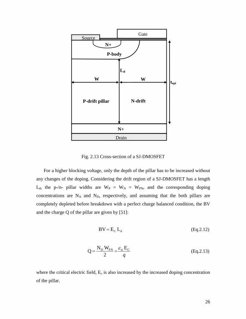
26
Fig. 2.13 Cross-section of a SJ-DMOSFET
For a higher blocking voltage, only the depth of the pillar has to be increased without
any changes of the doping. Considering the drift region of a SJ-DMOSFET has a length
Ld, the p-/n- pillar widths are WP = WN = WPN, and the corresponding doping
concentrations are NA and ND, respectively, and assuming that the both pillars are
completely depleted before breakdown with a perfect charge balanced condition, the BV
and the charge Q of the pillar are given by [51]:
dC LEBV (Eq.2.12)
q
CsiPND E
2
WNQ
(Eq.2.13)
where the critical electric field, Ec is also increased by the increased doping concentration
of the pillar.
W
P
P-body
Gate
Drain
Source
N+
N+
tepi W
N
P-drift pillar N-drift
pillar
Ld

27
Because the current flows only through the n-pillar, the specific on-resistance can be
expressed as [51]:
2Csin
PN
Dn
dsp on,
E 2
BVW
N q
LR
(Eq.2.14)
This equation clearly shows the linear relationship between the BV and the specific on-
resistance of SJ-DMOSFETs instead of the power relationship for the case of
conventional power MOSFETs. To achieve the best performance in the SJ structure,
precisely charge balanced p- /n- pillars must be formed at exactly the same doping level
to have equal amount of positive and negative charges. By carefully choosing the suitable
pillar width, doping concentration and drift region depth, the SJ device can substantially
outperform over the conventional power MOSFETs, especially in the medium to high
voltage ranges.
2.4.2 Current Status and Challenges of SJ Power MOSFETs
Several fabrication technologies have been implemented to realize SJ power
MOSFETs. The technologies and issues are briefly discussed in the following sections.
Multi-epitaxy technology [52-55]
This is the first technology used to fabricate the SJ device (i.e. COOLMOSTM
). The
devices were manufactured by multiple depositions of epitaxial layers and subsequent
boron and phosphorus implant process steps on a highly doped n+ substrate. The
diffusion process was followed to form vertically alternating n-/p- pillars. This is still
only available technology to fabricate the commercialized SJ power MOSFETs. Similar
to other SJ devices, it is quite difficult to achieve a perfect charge balance in the n-/p-
pillars. Any charge imbalance causes a degradation of the breakdown voltage. The
sensitivity of the BV to the charge imbalance is another difficulty in current
28
manufacturing environment. The multi-depositions of epitaxial layers are not compatible
with a standard CMOS process technology.
Deep Trench Etching with Vapor Phase Doping [56-58]
In this method, an n-type epitaxial layer was first grown on n+ substrates. After B+
ion implantation, a hexagonal trench was etched all the way down to the bottom of the
substrate and then boron is diffused into the sidewalls of the trench by using a Vapor
Phase Doping (VPD) process. A subsequent thermal annealing was required to drive-in
the boron impurities. The trenches were first deposited by thin dry oxide liners and then
gap-filled by TEOS deposition. Uniformity of p-pillar region formed by VPD process is
one of main processing issues. Also, the half of current conduction area in the drift region
is wasted by the TEOS gap-filling step.
Poly-Si Flanked VDMOS [59]
In this method, a thin thermal oxide liner was added between the n-/p- pillars as an
inter-diffusion barrier. Deep trenches were formed by etching n-epitaxial layer on the n+
substrate and then the thin oxide liner was grown inside the trenches. They were then
gap-filled with p-type polysilicon and then planarized by CMP process. Main issue
within this technology is that the quality of p-pillar region is even worse than the
epitaxial growth method. The polysilicon has a relatively high defect density in
comparison with a single crystalline Si-substrate or epitaxial layer. High temperature
annealing steps may reduce the defect densities (throughout the grain growth); however
the high thermal budget would result in the dopant redistribution. Also, it induces a stress
from various interfaces between the substrate and other deposited layers.
Deep Trench Etching and Selective Epitaxial Growth [60-62]
Similar to the deep trench etching with VPD process, the deep trenches were first
formed on the n-type epi wafer and then the trenches were filled by a selective epitaxial
growth (SEG) technique (e.g. p-type epi. silicon). The device was further improved with
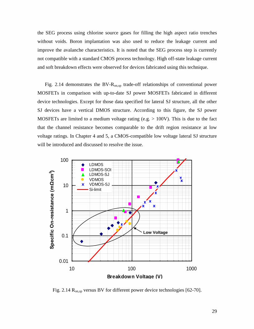
29
the SEG process using chlorine source gases for filling the high aspect ratio trenches
without voids. Boron implantation was also used to reduce the leakage current and
improve the avalanche characteristics. It is noted that the SEG process step is currently
not compatible with a standard CMOS process technology. High off-state leakage current
and soft breakdown effects were observed for devices fabricated using this technique.
Fig. 2.14 demonstrates the BV-Ron,sp trade-off relationships of conventional power
MOSFETs in comparison with up-to-date SJ power MOSFETs fabricated in different
device technologies. Except for those data specified for lateral SJ structure, all the other
SJ devices have a vertical DMOS structure. According to this figure, the SJ power
MOSFETs are limited to a medium voltage rating (e.g. > 100V). This is due to the fact
that the channel resistance becomes comparable to the drift region resistance at low
voltage ratings. In Chapter 4 and 5, a CMOS-compatible low voltage lateral SJ structure
will be introduced and discussed to resolve the issue.
Fig. 2.14 Ron,sp versus BV for different power device technologies [62-70].
0.01
0.1
1
10
100
10 100 1000
Breakdown Voltage (V)
Sp
ecif
ic O
n-r
esis
tan
ce (
mΩ
cm
2 )
LDMOS
LDMOS-SOILDMOS-SJ
VDMOSVDMOS-SJ
Si-limit
Low Voltage
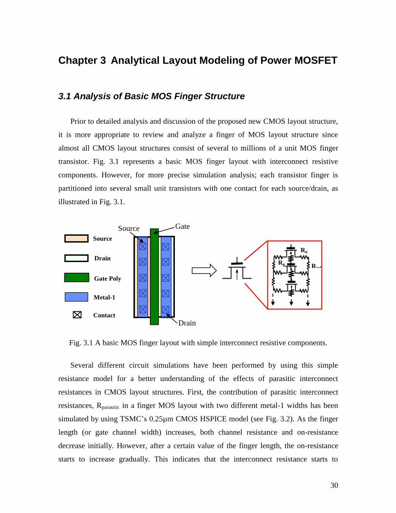
30
Chapter 3 Analytical Layout Modeling of Power MOSFET
3.1 Analysis of Basic MOS Finger Structure
Prior to detailed analysis and discussion of the proposed new CMOS layout structure,
it is more appropriate to review and analyze a finger of MOS layout structure since
almost all CMOS layout structures consist of several to millions of a unit MOS finger
transistor. Fig. 3.1 represents a basic MOS finger layout with interconnect resistive
components. However, for more precise simulation analysis; each transistor finger is
partitioned into several small unit transistors with one contact for each source/drain, as
illustrated in Fig. 3.1.
Fig. 3.1 A basic MOS finger layout with simple interconnect resistive components.
Several different circuit simulations have been performed by using this simple
resistance model for a better understanding of the effects of parasitic interconnect
resistances in CMOS layout structures. First, the contribution of parasitic interconnect
resistances, Rparasitic in a finger MOS layout with two different metal-1 widths has been
simulated by using TSMC‟s 0.25µm CMOS HSPICE model (see Fig. 3.2). As the finger
length (or gate channel width) increases, both channel resistance and on-resistance
decrease initially. However, after a certain value of the finger length, the on-resistance
starts to increase gradually. This indicates that the interconnect resistance starts to
Rc
Rm1 Rg
Drain
Source Gate
Source
Drain
Gate Poly
Contact
Metal-1
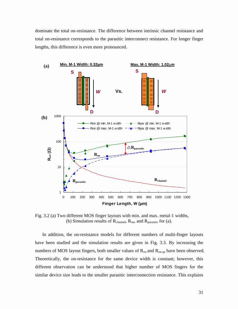
31
dominate the total on-resistance. The difference between intrinsic channel resistance and
total on-resistance corresponds to the parasitic interconnect resistance. For longer finger
lengths, this difference is even more pronounced.
Fig. 3.2 (a) Two different MOS finger layouts with min. and max. metal-1 widths,
(b) Simulation results of Rchannel, Ron, and Rparasitic for (a).
In addition, the on-resistance models for different numbers of multi-finger layouts
have been studied and the simulation results are given in Fig. 3.3. By increasing the
numbers of MOS layout fingers, both smaller values of Ron and Ron,sp have been observed.
Theoretically, the on-resistance for the same device width is constant; however, this
different observation can be understood that higher number of MOS fingers for the
similar device size leads to the smaller parasitic interconnection resistance. This explains
1
10
100
1000
0 100 200 300 400 500 600 700 800 900 1000 1100 1200 1300
Finger Length, W (µm)
Ro
n (
Ω)
Ron @ min. M-1 w idth Rpar @ min. M-1 w idth
Ron @ max. M-1 w idth Rpar @ max. M-1 w idth
Rchannel
Ron
Rparasitic
(a)
(b)
△Rparasitic
Vs.
Min. M-1 Width: 0.32µm Max. M-1 Width: 1.02µm
S
D
S
D
W W

32
why many layout designers do not always use the maximum finger length allowed in the
design rule. It is also interesting to note that a smaller technology node of standard
CMOS process provides the smaller on-resistance characteristics for the same device size.
Advanced CMOS technologies have more metal layers and this allows a greater reduction
in parasitic interconnect resistance.
Fig. 3.3 (a) Ron and (b) Ron,sp vs. Wtotal for different numbers of MOS fingers.
0
5
10
15
20
25
30
35
40
0 200 400 600 800 1000 1200 1400 1600 1800 2000
Total Finger Length, Wtotal (µm)
Ro
n,s
p (m
Ω·m
m2)
Ref[48] (0.8um)
1 finger (TSMC 0.25um)
3 fingers (TSMC 0.25um)
10 fingers (TSMC 0.25um)
20 fingers (TSMC 0.25um)Ref. 0.8µm CMOS [71]
1 finger 3 fingers 10 fingers
20 fingers
(b) [71]
1
10
100
1000
0 200 400 600 800 1000 1200 1400 1600 1800 2000
Total Finger Length, W total (µm)
Ro
n (
Ω)
Ref [48] (0.8um)
1 finger (TSMC 0.25um)
3 fingers (TSMC 0.25um)
10 fingers (TSMC 0.25um)
20 fingers (TSMC 0.25um)
Ref. 0.8µm CMOS [71]
1 finger
3 fingers
10 fingers
20 fingers
(a) [71]
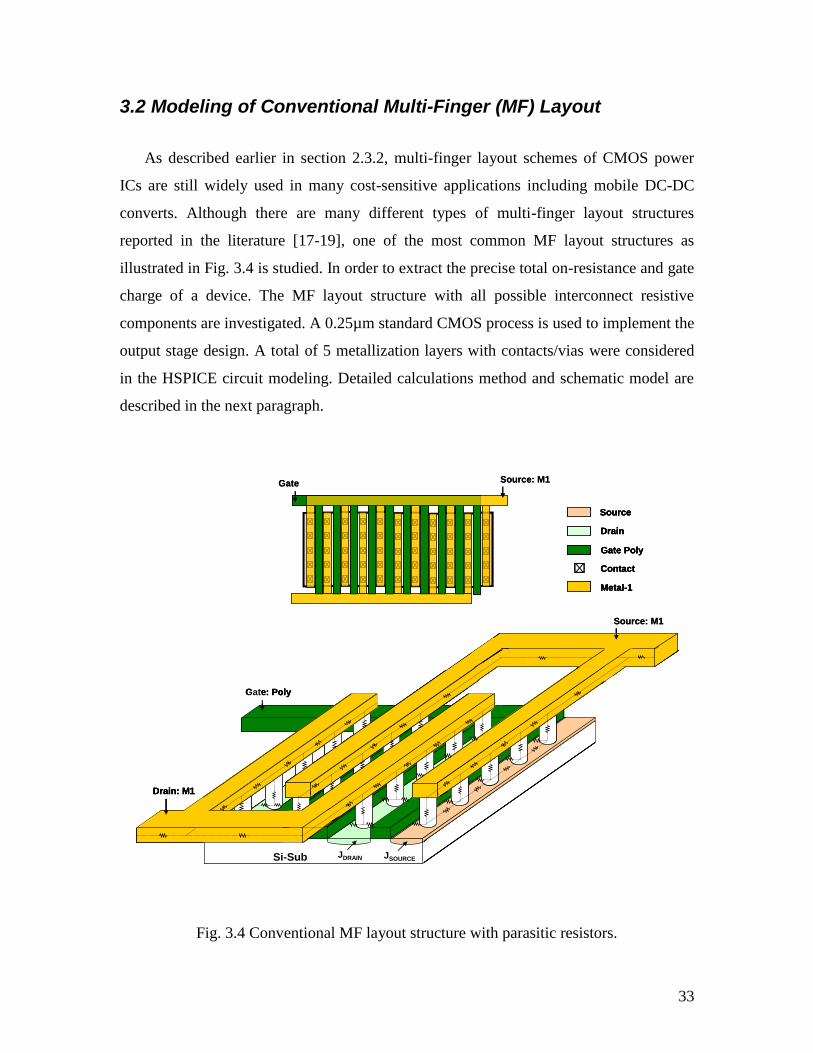
33
3.2 Modeling of Conventional Multi-Finger (MF) Layout
As described earlier in section 2.3.2, multi-finger layout schemes of CMOS power
ICs are still widely used in many cost-sensitive applications including mobile DC-DC
converts. Although there are many different types of multi-finger layout structures
reported in the literature [17-19], one of the most common MF layout structures as
illustrated in Fig. 3.4 is studied. In order to extract the precise total on-resistance and gate
charge of a device. The MF layout structure with all possible interconnect resistive
components are investigated. A 0.25µm standard CMOS process is used to implement the
output stage design. A total of 5 metallization layers with contacts/vias were considered
in the HSPICE circuit modeling. Detailed calculations method and schematic model are
described in the next paragraph.
Fig. 3.4 Conventional MF layout structure with parasitic resistors.
Gate Source: M1
Source
Drain
Gate Poly
Contact
Metal-1
Source: M1
Drain: M1
Gate: Poly
JSOURCEJDRAINSi-Sub
Gate Source: M1
Source
Drain
Gate Poly
Contact
Metal-1
Source
Drain
Gate Poly
Contact
Metal-1
Source: M1
Drain: M1
Gate: Poly
JSOURCEJDRAINSi-Sub
Drain: M1
Gate: Poly
JSOURCEJDRAINSi-Sub

34
TSMC‟s 0.25µm standard CMOS process provides two different types of transistors;
(a) 2.5V logic thin gate oxide MOSFETs and (b) 5V high-voltage I/O thick gate oxide
MOSFETs. Two important differences between transistors (a) and (b) are the breakdown
voltage (BV) and the minimum channel length, Lgate of the MOSFET. Since our target
specifications require an actual 7V-BV, the 5V thick gate oxide MOSFET was only
option for the final DC-DC converter output stage design. It is noted that the minimum
drawn channel length of the thick gate oxide transistor is 0.5µm, which is the twice as
long as the minimum channel length of the 2.5V logic transistor in TSMC‟s 0.25µm
standard CMOS process. By carefully examining the given minimum design rules of the
thick gate oxide transistors, a MF layout structure with 10 gate fingers was first
constructed and then a corresponding model with various resistive components was
developed as demonstrated in Fig. 3.5 and Fig. 3.6, respectively.
The calculation methods for these resistors are quite straight forward since there are
only two different directions of current flowing; lateral and vertical. For the vertical
direction, the corresponding resistive component can be estimated by contact/via
resistances. By adding more number of contacts (or vias) in parallel, the vertical
resistance between top and bottom layers can be simplified as: Rvertical = (Rcontact for a
contact) / (# of contacts). For the lateral direction, the corresponding resistance is mainly
from a metal layer. Since the sheet resistance of each metal layer is provided from the
foundry technology file, the lateral resistance on each metal layer can be simplified as:
Rlateral = Rsheet (Lmetal/Wmetal). Based on these two simple calculation methods, each
interconnect resistor denoted in Fig. 3.6 was extracted for the model. More detailed
information on all these calculations can be found in Appendix-I.
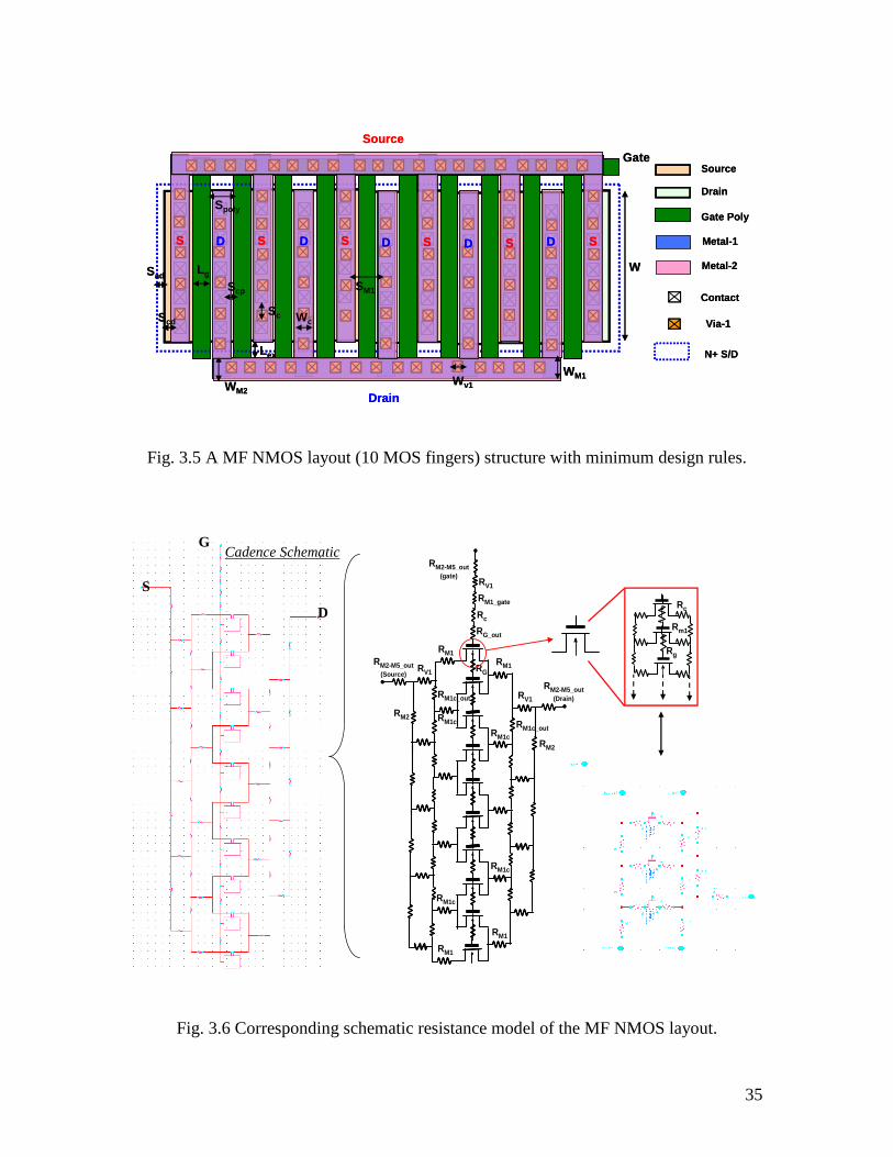
35
Fig. 3.5 A MF NMOS layout (10 MOS fingers) structure with minimum design rules.
Fig. 3.6 Corresponding schematic resistance model of the MF NMOS layout.
Rc
Rm1
Rg
RG
RG_out
RM1
RM1c
RM1c_out
RV1
RM2
RM2-M5_out
(Drain)
RM1
RM1c
RM1c_out
RV1
RM2
RM1
RM1
RM1c
RM1c
RM2-M5_out
(Source)
Rc
RM1_gate
RV1
RM2-M5_out
(gate)
Cadence Schematic
S
D
G
Source
Drain
Gate Poly
Contact
Metal-1
Metal-2
Via-1
N+ S/D
Source
Drain
Gate Poly
Contact
Metal-1
Metal-2
Via-1
N+ S/D
Lg
Drain
Source
Gate
WM2
Wc
W
S D S SSD SD SD D
WM1
Scd
Sad
Spoly
Sc
Scp
Lex
Wc
SM1
Wv1
Lg
Drain
Source
Gate
WM2
Wc
W
S D S SSD SD SD DS D S SSD SD SD D
WM1
Scd
Sad
Spoly
Sc
Scp
Lex
Wc
SM1
Wv1

36
3.3 Modeling of Regular Waffle (RW) Layout
As previously discussed in the section 2.3.2, a regular waffle layout (RW) design was
invented to maximize the active channel width for a given area. By sharing a source/drain
contact with four surrounding transistors, the RW layout has offered a lower Ron in
comparison to that of MF. However, for large size RW devices, the metal lines used to
connect the source and drain are of very long and narrow dimensions, leading to
excessive parasitic series resistance. As a result, the advantage of RW layout structure is
quickly diminished.
To validate the performance differences between RW and MF structures in a standard
0.25µm CMOS process, the resistance model for a RW layout structure was developed.
Fig. 3.7 represents a 44 RW layout structure with the corresponding resistance model.
The minimum width of a unit transistor in the RW layout was calculated as 0.74 µm by
considering the minimum diffusion length, contact size, and gate poly width. The detailed
calculations for each interconnect resistor can be seen in Appendix-I. By analyzing the
minimum design rules, the actual device size and total width required for a specific RW
layout structure can be also extracted from the model. Different sizes of RW layout
structures are summarized in Table 3.1.
Table 3.1 Data for different NN matrix of RW layout structures
W
(µm)
L
(µm)
Wtotal
(µm)
Die Size
(mm2)
Unit-cell
Pitch (µm)
# of unit cells
in x-axis
# of unit cells
in y-axis 0.74 0.50 133 0.0002 1.24 10 10
0.74 0.50 562 0.0006 1.24 20 20
0.74 0.50 3626 0.0039 1.24 50 500
0.74 0.50 14652 0.0155 1.24 100 100
0.74 0.50 58904 0.0618 1.24 200 200
0.74 0.50 132756 0.1388 1.24 300 300
Notes
Unit-cell Pitch = W + 2(L/2) = W + L = W + 0.5µm = 1.24µm
Wtotal = W × (Total # of MOS Fingers) = W × 2[(# of Unit-cells in x-/y-axis)2 – (# of Unit-cells in y-axis)]
Die Size = [(Unit-cell Pitch) × (# of Unit-cell in x-/y-axis) + 0.5]2 × (0.001)
2

37
Fig. 3.7 Schematic of (a) 44 regular waffle layout and (b) the corresponding resistance
model.
Source: M-1 || M-5
Gate Poly
Drain: M-1 || M-5
Lg
W
Scp
Wc,v1-v4
WM1-M5
Sc-c
(a)
4RcSource
Drain RM1 || M5
Rout
Rroute
Rroute
Rout
Rroute
4Rv1-4
(b)
Unit-cell

38
3.4 Proposed Hybrid Waffle (HW) Layout
In the hybrid waffle layout as illustrated in Fig. 3.8(a), the unit transistor widths are
designed to be several times wider than the minimum contact size allowed. Similar to the
conventional waffle layout structures, the HW layout structure also maximizes the active
channel width by sharing a source/drain contact with four surrounding transistors,
however, the much of layout area is occupied by metal interconnection rather than the
active area. The basic idea of HW layout came from [72] such that the wider metal
interconnections can lower the overall on-resistance of the power transistors, especially
for low voltage CMOS devices. In addition, the reduced overall device width and
source/drain junctions will result in a lower gate and parasitic capacitance. Detailed
calculation methods for each parasitic resistor denoted in Fig. 3.8(b) can be seen in
Appendix-I. Also, Table 3.2 summarizes the total width and die size required for different
NN matrix of HW layout structures. Since all parameters are a function of the MOS
finger length, several different values were considered in the simulation to find out if
there exists an optimal Lfinger value or not. More details will be given in the next
following section.
Table 3.2 Data for different NN matrix of HW layout structures
W
(µm)
L
(µm)
Wtotal
(µm)
Die Size
(mm2)
Unit-cell
Pitch
(µm)
# of unit
cells in x-
axis
# of unit
cells in y-
axis
5.0 0.50 900 0.0049 6.82 10 10
5.0 0.50 2100 0.0108 6.82 15 15
5.0 0.50 3800 0.0191 6.82 20 20
5.0 0.50 6000 0.0297 6.82 25 25
5.0 0.50 8700 0.0426 6.82 30 30
5.0 0.50 11900 0.0578 6.82 35 35
5.0 0.50 15600 0.0754 6.82 40 40
5.0 0.50 19800 0.0953 6.82 45 45
5.0 0.50 24500 0.1175 6.82 50 50
5.0 0.50 29700 0.1421 6.82 55 55
5.0 0.50 35400 0.1689 6.82 60 60
Notes
Unit-cell Pitch = W + 2(0.22) + 2(0.14) + 2(0.3) + 0.5 = 6.82µm
Wtotal = W × (Total # of MOS Fingers) = W × 2[(# of Unit-cells in x-/y-axis)2 – (# of Unit-cells in y-axis)]
Die Size = [(Unit-cell Pitch) × (# of Unit-cell in x-/y-axis) + 0.5 + 2(0.22) + 2(0.3) + 2(0.14)]2 × (0.001)
2

39
Fig. 3.8 Hybrid waffle structure: (a) a layout and (b) a corresponding resistance model.
GS
D
GS
D
G
D
S
G
D
S
Rc
RM1-CtV
Rx1
= (Rv1 + RM2 +Rv2)
Rroute
Rout
RM3 || M5
(a)
(b)
Rroute
SC
WM3
W
Lg
Lex
SM3
LM3
Ld
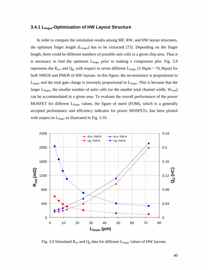
40
3.4.1 Lfinger-Optimization of HW Layout Structure
In order to compare the simulation results among MF, RW, and HW layout structures,
the optimum finger length (Lfinger) has to be extracted [73]. Depending on the finger
length, there could be different numbers of possible unit cells in a given chip area. Thus it
is necessary to find the optimum Lfinger prior to making a comparison plot. Fig. 3.9
represents the Ron, and Qg, with respect to seven different Lfinger (3.36µm ~ 76.36µm) for
both NMOS and PMOS of HW layouts. In this figure, the on-resistance is proportional to
Lfinger and the total gate charge is inversely proportional to Lfinger. This is because that the
larger Lfinger, the smaller number of units cells (or the smaller total channel width, Wtotal)
can be accommodated in a given area. To evaluate the overall performance of the power
MOSFET for different Lfinger values, the figure of merit (FOM), which is a generally
accepted performance and efficiency indicator for power MOSFETs, has been plotted
with respect to Lfinger as illustrated in Fig. 3.10.
Fig. 3.9 Simulated Ron and Qg data for different Lfinger values of HW layouts.
0
0.04
0.08
0.12
0.16
0.2
0.24
0
400
800
1200
1600
2000
2400
0 10 20 30 40 50 60 70 80
QG
(nC
)
RO
N(m
Ω)
Lfinger (µm)
Ron: NMOS Ron: PMOS
Qg: NMOS Qg: PMOS

41
Fig. 3.10 FOM-1 & FOM-2 versus different Lfinger of HW layout structures.
In Fig. 3.10, two different FOMs: FOM-1= Ron x Qg, FOM-2= Ron,sp x Qg, (Ron,sp =
Ron Area) are represented. Both NMOS and PMOS have the minimum FOM value
when Lfinger is close to 5 ~ 12 µm. Although a small FOM value of the power MOSFET
generally leads to higher power efficiency, however it is suspected that this may not be a
good performance indicator for a low voltage CMOS technology since low voltage
CMOS processes have a much smaller total gate charge, Qg value. Hence, the optimum
Lfinger is more accurately verified from the power efficiency versus Lfinger plot for a
constant load current. The efficiency simulation results of both SPICE and MATLAB
give an optimal Lfinger of approximately 5 µm. It is noted that all DC-DC converter
efficiency simulation and gate drive/controller design works for the final output stage
were done by Marian Chang [74], a MASc student whom I worked together for the same
research project from ON-Semiconductor Corp.
0
3
6
9
12
15
18
21
24
0
10
20
30
40
50
60
70
80
0 10 20 30 40 50 60 70 80
FO
M-2
(n
C∙m
Ω∙m
m2)
FO
M-1
(n
C∙m
Ω)
Lfinger (µm)
FOM-1: NMOS FOM-1: PMOS
FOM-2: NMOS FOM-2: PMOS

42
3.4.2 Performance Evaluation via FOM
In the previous section, the conventional FOM was suspected as not a good
performance indicator for a low voltage CMOS technology. As a result, the further
investigations on the suitability of this FOM for different power MOSFET structures are
carried out in this section. Conventional trench gate and lateral diffusion MOSFETs with
similar voltage ratings and operating conditions are carefully selected from several
manufactures for a comparative analysis of FOMs. For trench gate and other
conventional lateral diffusion power transistors, the high side and low side switches are
chosen separately as they are packaged individually. In this evaluation, a single p-channel
power MOSFET is selected as the high side switch in combination with different n-
channel power MOSFETs as the low side switch. This simplifies the output stage
evaluation regarding the n-channel power MOSFET. The device specifications and
typical operating conditions stated in the datasheets are summarized in both Table 3.3 and
Table 3.4.
Table 3.3 Parameter Summary of Trench-Gate Power MOSFETs
Trench-Gate
power NMOS Si5920DC Si1450DH Si8424DB SiA414DJ Si1050X Si8404DB
Vds (V) 8 8 8 8 8 8
Vgs (V) 5 5 5 5 5 5
Ron @ 4.5V (Ω) 0.032 0.047 0.031 0.011 0.086 0.031
Qg @ 4.5V (nC) 7.3 4.24 20 19 7.1 20
QRR (nC) 3 3.6 88 20 3.7 88
Vf (V) 0.8 0.8 0.6 0.8 0.8 0.6
IL (A) 4 4 12.2 12 1.34 12.2
FOM 234 199 620 209 611 620
Datasheet [75] [76] [77] [78] [79] [80]
Table 3.4 Parameter Summary of Lateral-Diffusion Power MOSFETs
n-type LDMOS MGSF1N02LT1 MMBF0201NLT1 NTA4153N NTK3134N
Vds (V) 20 20 20 20
Vgs (V) 12 12 6 6
Ron @ 4.5V (Ω) 0.115 1 0.127 0.2
Qg @ 4.5V (nC) 3 1.4 1.82 1.16
QRR (nC) 5 5 3 3
Vf (V) 0.8 0.85 0.67 0.75
IL (A) 1 0.3 0.6 0.89
FOM 345 1400 230 232
Datasheet [81] [82] [83] [84]

43
From the datasheets, the dynamic characteristics of these conventional power
MOSFETs were evaluated at 1MHz and the efficiency simulation was performed with the
conditions summarized in Table 3.5. With these operating conditions, a current-
programmed control loop was designed by Marian Chang [74] to achieve a phase margin
of around 60 degrees, and a cut-off frequency of one-fifteenth to one-tenth of the
switching frequency. The results were plotted in Fig. 3.11. As expected, an inversely
proportional relationship was found in those two different devices. This indicates that the
conventional FOM, which is a product of Ron and Qg, is an effective performance
indicator for output stages designed with trench gate and lateral diffusion MOSFETs.
Table 3.5 Efficiency Simulation Conditions: Conventional Power MOSFETs
Parameters Simulator values for Trench MOS Simulator values for LDMOS
Vds 4.5V 4.5V
Vgs 4.5V 4.5V
Vout 1.8V 1.8V
IL Nominal IL Nominal IL
fs 400 kHz, 800kHz, and 1.2MHz 500 kHz, 1MHz, and 1.5MHz
Fig. 3.11 FOM vs. Efficiency for conventional power MOSFETs.
70
75
80
85
90
95
0 300 600 900 1200 1500
Eff
icie
ncy (
%)
FOM (nC∙mΩ)
Trench MOS
LDMOS
@ fs = 1 MHz
@ fs = 800 kHz

44
A similar analysis of efficiency vs. conventional FOM was performed for CMOS-
based power MOSFETs with different total gate widths implemented in Cadence
Virtuoso. Both Ron and Qg were extracted through HSPICE simulation and the detailed
simulation conditions are summarized in Appendix-II. The extracted values for different
NMOSFETs are listed in Table 3.6. For a comparison with efficiency, the conventional
FOM was first calculated for each NMOSFET. The efficiency simulation of these
converters was performed with test conditions summarized in Table 3.7. The simulation
results of power conversion efficiency are plotted in Fig. 3.12 with respect to the
conventional FOM.
Table 3.6 Parameter Summary of CMOS-based Power MOSFETs
CMOS Power NMOS #1 #2 #3 #4 #5 #6
Total Gate Width (mm) 8.7 11.9 15.6 19.8 24.5 29.7
Vds Breakdown Voltage (V) 7
Vgs (V) 5.5
Ron @ 3.3V (mΩ) 330 245 195 165 149 147
Qg @ 3.3V (nC) 0.038 0.052 0.068 0.086 0.106 0.129
QRR (nC) 1
Vf (V) 0.6
IL (A) 0.4
FOMConventional 12.44 12.63 13.18 14.16 15.82 18.92
Table 3.7 Efficiency Simulation Conditions: CMOS-based Power MOSFETs
Parameters Simulator values
Vds 3.3V
Vgs 3.3V
Vout 0.8V
IL 0.4 A
fs 5 MHz, 10MHz, and 15MHz
In contrast to the simulated result in Fig. 3.11, the conventional FOM was found to be
clearly not a good performance indicator for CMOS-based power MOSFETs. The lower
FOM value no longer guarantees a higher efficiency or better design performance. This
observation can be understood through the difference in device structure. As illustrated in
Fig. 3.13, standard CMOS inherently has a much smaller overlap area between its poly-
silicon gate electrode and the source/drain diffusion area than the conventional power
MOSFETs. Therefore, CMOS-based power MOSFETs have a smaller Qg, and a different
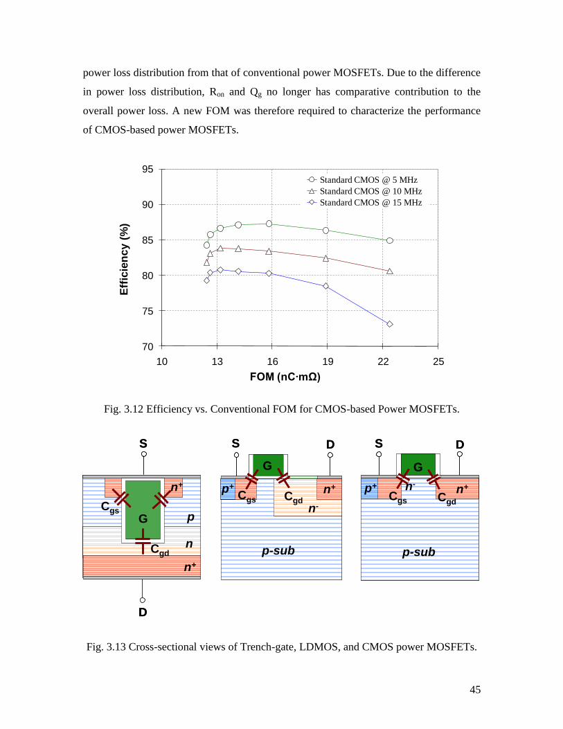
45
power loss distribution from that of conventional power MOSFETs. Due to the difference
in power loss distribution, Ron and Qg no longer has comparative contribution to the
overall power loss. A new FOM was therefore required to characterize the performance
of CMOS-based power MOSFETs.
Fig. 3.12 Efficiency vs. Conventional FOM for CMOS-based Power MOSFETs.
Fig. 3.13 Cross-sectional views of Trench-gate, LDMOS, and CMOS power MOSFETs.
n
n+
Cgs
p-sub
p+
D
S
Cgd
Cgs
n+
p
n+n-
Cgd
G
G
DSDS
p+ n+
n-
p-sub
G
Cgs Cgd
n
n+
Cgs
p-sub
p+
D
S
Cgd
Cgs
n+
p
n+n-
Cgd
G
G
DSDS
p+ n+
n-
p-sub
G
Cgs Cgd
70
75
80
85
90
95
10 13 16 19 22 25
Eff
icie
ncy (
%)
FOM (nC∙mΩ)
Standard CMOS @ 5 MHz
Standard CMOS @ 10 MHz
Standard CMOS @ 15 MHz

46
New Figure of Merit (FOM)
From the literature review in [85], Colino and Schultz proposed a new FOM method
using different weighting factors for each FOM element which depends on a specific
topology and circuit conditions. However, they have not specified on how these
weighting factors can be chosen. In this section, a systematic approach is developed by
analyzing the major loss mechanisms in a synchronous buck converter to determine these
weighting factors.
For different DC-DC converter topologies, various power loss equations can be used
to determine the weighting factors of the new FOM. Although the weights of the
conduction loss and gate-drive loss for CMOS-based power MOSFETs are different from
those for conventional power MOSFETs, they are still two the major power loss
contributing factors [86]. Hence, Ron and Qg are also two important key parameters to be
considered for characterization. The new FOM equation can be defined as:
gONNew QBRAFOM (Eq.3.1)
where Aand B are the weighting factors. To determine the values of these weighting
factors, the equation for conduction and gate-drive loss are stated [2]:
DRIP HSONLHScond )(2
)( Conduction loss: HS switch
)1()(2
)( DRIP LSONLLScond Conduction loss: LS switch
SLSgHSggggate fQQVP )( )()( Total gate-drive loss
condP is proportional to the square of output load current. By assuming that the HS and
LS switches have similar Ron as they are generally designed to be for CMOS power
MOSFETs, the constant A in Eq.3.1 is the square of the typical output load current. The
assumption of similar Ron for both the HS and LS switches is quite reasonable when the
duty cycle is not always much above or much below 50%. To further illustrate the design

47
decision, one can consider an application where Vout varies from 1.8 to 3.3V when Vin is
held at 5.5V. In this case, the duty cycle varies from 36% to 66%, thus the conduction
time for both the HS and LS switches would be comparable over the operating range.
This indicates that their on-resistances should also be designed to have comparable values.
When choosing an appropriate power MOSFET for a specific application, the designers
are usually aware of the operating switching frequency (fs) and the supply voltage level
(Vin). Hence, these two parameters can be used to calculate the weighting factor of Qg. In
order to account for the total Qg from both the HS and LS switches when only the Qg of
the LS switch is known, it is necessary to note that Qg of a PMOS is about three times
larger than that of an NMOS. Since the effective mass of a hole is much larger than that
of an electron, this results in a lower mobility for hole. By considering this fact, the
PMOS switch should be approximately three times larger than the NMOS to achieve
similar Ron. Therefore, the total Qg would be approximately four times of Qg (LS). This can
be reflected by defining the constant B in Eq.3.2.
inS VfB 4 (Eq.3.2)
Nevertheless, if Qg for the PMOS is known, it can be included as the total Qg, and the
constant B will not require a scaling factor of 4. Simultaneously, SPICE simulation for
Qg extraction may not produce an accurate value of Qg when the size of PMOS is too
large. When only Qg of NMOS is extracted, the new FOM equation can be defined as:
)()(2 4 LSginSLSONLNew QVfRIFOM (Eq.3.3)
To confirm the validity of the proposed FOM, the efficiency (as plotted in Fig. 3.12)
vs. the new FOM for the CMOS-based power MOSFETs is re-plotted in Fig. 3.14. In
contrast to the traditional FOM, the new FOM data trend represents the corresponding
power conversion efficiency more accurately [87]. This can be explained by the fact that
the new FOM reflects the conduction and switching power losses more effectively as it
has a unit in watt. Therefore, this new FOM developed for low voltage CMOS transistors
is a more accurate indicator of the overall device performance.
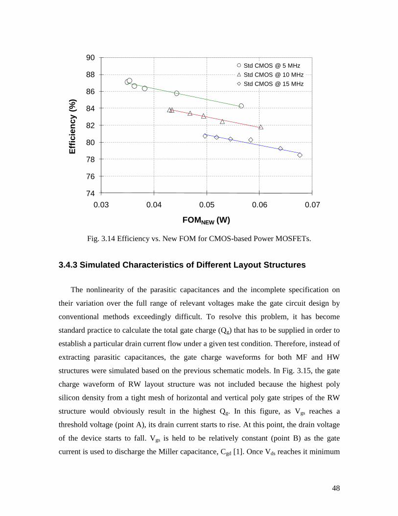
48
Fig. 3.14 Efficiency vs. New FOM for CMOS-based Power MOSFETs.
3.4.3 Simulated Characteristics of Different Layout Structures
The nonlinearity of the parasitic capacitances and the incomplete specification on
their variation over the full range of relevant voltages make the gate circuit design by
conventional methods exceedingly difficult. To resolve this problem, it has become
standard practice to calculate the total gate charge (Qg) that has to be supplied in order to
establish a particular drain current flow under a given test condition. Therefore, instead of
extracting parasitic capacitances, the gate charge waveforms for both MF and HW
structures were simulated based on the previous schematic models. In Fig. 3.15, the gate
charge waveform of RW layout structure was not included because the highest poly
silicon density from a tight mesh of horizontal and vertical poly gate stripes of the RW
structure would obviously result in the highest Qg. In this figure, as Vgs reaches a
threshold voltage (point A), its drain current starts to rise. At this point, the drain voltage
of the device starts to fall. Vgs is held to be relatively constant (point B) as the gate
current is used to discharge the Miller capacitance, Cgd [1]. Once Vds reaches it minimum
74
76
78
80
82
84
86
88
90
0.03 0.04 0.05 0.06 0.07
Eff
icie
ncy (
%)
FOMNEW (W)
Std CMOS @ 5 MHz
Std CMOS @ 10 MHz
Std CMOS @ 15 MHz
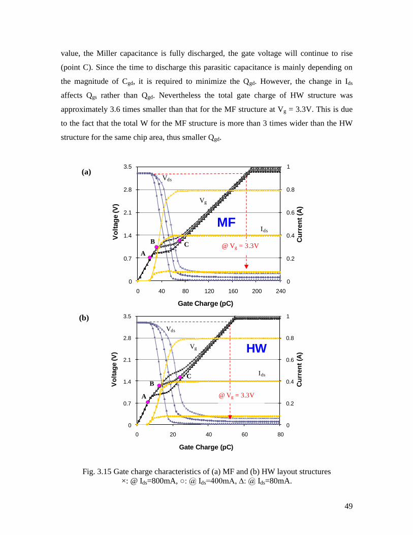
49
value, the Miller capacitance is fully discharged, the gate voltage will continue to rise
(point C). Since the time to discharge this parasitic capacitance is mainly depending on
the magnitude of Cgd, it is required to minimize the Qgd. However, the change in Ids
affects Qgs rather than Qgd. Nevertheless the total gate charge of HW structure was
approximately 3.6 times smaller than that for the MF structure at Vg = 3.3V. This is due
to the fact that the total W for the MF structure is more than 3 times wider than the HW
structure for the same chip area, thus smaller Qgd.
Fig. 3.15 Gate charge characteristics of (a) MF and (b) HW layout structures
×: @ Ids=800mA, ○: @ Ids=400mA, ∆: @ Ids=80mA.
0
0.2
0.4
0.6
0.8
1
0
0.7
1.4
2.1
2.8
3.5
0 40 80 120 160 200 240
Cu
rren
t (A
)
Vo
ltag
e (V
)
Gate Charge (pC)
Vg
Vds
Ids
MF
@ Vg = 3.3V
0
0.2
0.4
0.6
0.8
1
0
0.7
1.4
2.1
2.8
3.5
0 20 40 60 80
Cu
rren
t (A
)
Vo
ltag
e (V
)
Gate Charge (pC)
Vg
Vds
Ids
@ Vg = 3.3V
HW
(a)
(b)
A
B C
A
B C
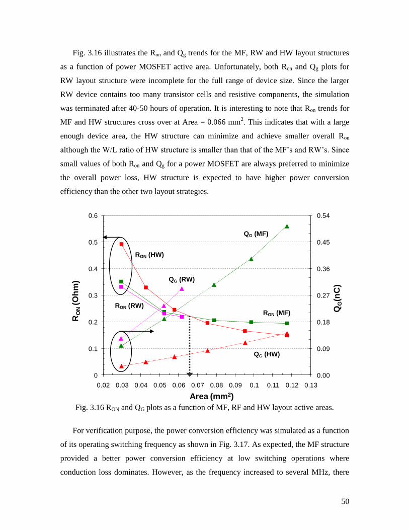
50
Fig. 3.16 illustrates the Ron and Qg trends for the MF, RW and HW layout structures
as a function of power MOSFET active area. Unfortunately, both Ron and Qg plots for
RW layout structure were incomplete for the full range of device size. Since the larger
RW device contains too many transistor cells and resistive components, the simulation
was terminated after 40-50 hours of operation. It is interesting to note that Ron trends for
MF and HW structures cross over at Area = 0.066 mm2. This indicates that with a large
enough device area, the HW structure can minimize and achieve smaller overall Ron
although the W/L ratio of HW structure is smaller than that of the MF‟s and RW‟s. Since
small values of both Ron and Qg for a power MOSFET are always preferred to minimize
the overall power loss, HW structure is expected to have higher power conversion
efficiency than the other two layout strategies.
Fig. 3.16 RON and QG plots as a function of MF, RF and HW layout active areas.
For verification purpose, the power conversion efficiency was simulated as a function
of its operating switching frequency as shown in Fig. 3.17. As expected, the MF structure
provided a better power conversion efficiency at low switching operations where
conduction loss dominates. However, as the frequency increased to several MHz, there
0.00
0.09
0.18
0.27
0.36
0.45
0.54
0
0.1
0.2
0.3
0.4
0.5
0.6
0.02 0.03 0.04 0.05 0.06 0.07 0.08 0.09 0.1 0.11 0.12 0.13
QG(n
C)
RO
N(O
hm
)
Area (mm2)
RON (HW)
QG (HW)
QG (MF)
QG (RW)
RON (MF) RON (RW)
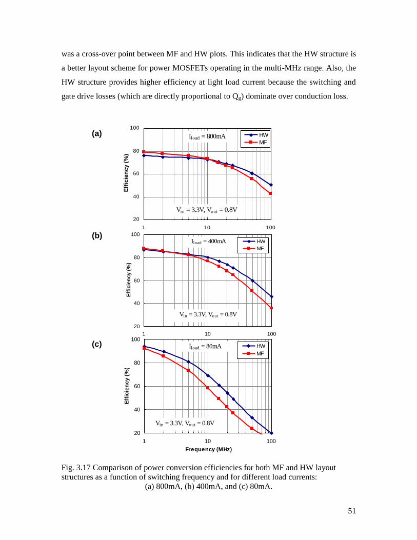
51
was a cross-over point between MF and HW plots. This indicates that the HW structure is
a better layout scheme for power MOSFETs operating in the multi-MHz range. Also, the
HW structure provides higher efficiency at light load current because the switching and
gate drive losses (which are directly proportional to Qg) dominate over conduction loss.
Fig. 3.17 Comparison of power conversion efficiencies for both MF and HW layout
structures as a function of switching frequency and for different load currents:
(a) 800mA, (b) 400mA, and (c) 80mA.
20
40
60
80
100
1 10 100
Frequency (MHz)
Eff
icie
ncy (
%)
HW
MF
Vin = 3.3V, Vout = 0.8V
Iload = 800mA
20
40
60
80
100
1 10 100
8
Eff
icie
ncy (
%)
HW
MF
Vin = 3.3V, Vout = 0.8V
Iload = 400mA
(a)
(b)
(c)
20
40
60
80
100
1 10 100
Frequency (MHz)
Eff
icie
ncy (
%)
HW
MF
Vin = 3.3V, Vout = 0.8V
Iload = 80mA

52
In comparison with the MF and RW layouts, the HW structure demonstrates smaller
FOM even though its overall on-resistance at the small die area is higher than that of
MF‟s and RW‟s. This is due to a relatively smaller QG data of HW structures, as
summarized in Table 3.8.
Table 3.8 Simulation Data Summary of MF, RW, and HW Layout Structures
NMOS @ Vin=3.3V, Vdd=3.3V, Id=400mA
L
(µm)
Wtotal
(µm)
Area
(mm2)
Ton
(ps)
Toff
(ps)
RON
(mΩ)
QG
(nC)
FOM
(nC·mΩ)
Multi-
Fingers
(MF)
0.50 20172 0.0295 15.5 214.9 352 0.099 34.80
0.50 36388 0.0523 25.7 472.8 237 0.190 44.96
0.50 54582 0.0788 38.4 914.2 206 0.306 63.00
0.50 71354 0.0985 68.9 1452.2 199 0.393 78.16
0.50 86520 0.1175 118.1 2370.3 194 0.504 97.71
Regular
Waffle
(RW)
0.50 27981 0.0295 18.6 305.2 332 0.137 45.48
0.50 49835 0.0523 37.1 882.7 231 0.260 60.06
0.50 58904 0.0618 N/A N/A 219 0.324 70.96
Hybrid
Waffle
(HW)
0.50 6000 0.0297 9.8 108.5 493 0.030 14.78
0.50 8700 0.0426 17.8 168.5 330 0.044 14.50
0.50 11900 0.0578 30.2 261.4 245 0.061 15.01
0.50 15600 0.0754 41.1 325.6 195 0.083 16.12
0.50 19800 0.0953 53.6 437.9 165 0.109 17.97
0.50 24500 0.1175 68.4 554.2 149 0.141 20.99

53
3.5 Summary
This chapter presented the simulation-based research on a low-voltage CMOS power
transistor layout technique, implemented in a 0.25µm standard CMOS technology that is
suitable for high speed switching power devices. The proposed hybrid waffle (HW)
layout technique organizes MOSFET fingers in a square grid arrangement. It was
designed to provide an effective trade-off between the width of diagonal source/drain
metal and the active device area, allowing more effective optimization between switching
and conduction losses. In comparison with conventional multi-finger (MF) layout
geometries, the HW layout structure for the power MOSFET was found to exhibit
approximately 30% reduction in overall on-resistance with 3.6 times smaller total gate
charge for CMOS devices with a current rating of 1A. Moreover, it was found that the
conventional FOM was no longer a suitable indicator of overall device performance,
especially for the low voltage CMOS power transistors. Therefore, a new FOM was
proposed to model specifically the power loss distribution for the CMOS output-stages.
By adding two different weighting factors for both conduction and switching losses, the
new FOM could reflect the overall device performance more accurately. Lastly, the
integrated output-stage using the HW structure could achieve higher simulated power
conversion efficiencies at switching frequencies beyond multi-MHz. This performance
gain was obtained without additional processing step or changes in a device structure, and
will be very attractive for next generation low voltage integrated power converters.

54
Chapter 4 High Speed CMOS Output Stage for Integrated
DC-DC Converter
To increase the speed and decrease the power consumption of microprocessors, the
integrated DC-DC converter should operate with high efficiency. Although much effort
has gone toward improving the performance of the converter through advanced circuit
designs [17-21], the most convenient way to optimize the power MOSFET is most likely
by changing the layout structure without any variation of fabrication process. The
previous chapter has introduced a new layout strategy named “Hybrid Waffle” power
MOSFETs and compared the simulated performances of several different schematic
models. However, the best way to confirm actual device performance is by testing the
fabricated device. In this chapter, HW power MOSFET arrays with connection routing,
ESD protection, power clamps, and I/O pads are designed, fabricated and tested to
achieve the target specification list in Table 4.1.
Table 4.1 Target Specification
Maximum Die Size 1.68mm2 (1.4mm x 1.2mm)
MOSFET Features
Input Voltage Range (V) 2.5 to 5.5
Max. Output Current (mA) 800
Peak Current Limit (A) 1.2
Frequency Operating Range (MHz) Min: 2 Typical: 10 Max: 12
P-channel On-resistance (mΩ)
VIN = 3.3, ILOAD = 400mA 210
N-channel On-resistance (mΩ)
VIN = 3.3, ILOAD = 400mA 120
Absolute Maximum Ratings
Minimum Voltage All Pins (V) -0.3
Maximum Voltage All Pins (V) 6
Maximum Operating Voltage All Pins (V) 6
Operating Ambient Temperature Range (oC) -40 to 85
Storage Temperature Range -55 to 150
Junction Operating Temperature -40 to 125
ESD Withstand Voltage
Human Body Model (kV)
Machine Model (V)
2.0
400
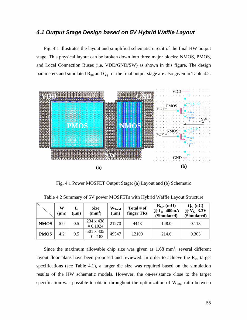
55
4.1 Output Stage Design based on 5V Hybrid Waffle Layout
Fig. 4.1 illustrates the layout and simplified schematic circuit of the final HW output
stage. This physical layout can be broken down into three major blocks: NMOS, PMOS,
and Local Connection Buses (i.e. VDD/GND/SW) as shown in this figure. The design
parameters and simulated Ron and Qg for the final output stage are also given in Table 4.2.
Fig. 4.1 Power MOSFET Output Stage: (a) Layout and (b) Schematic
Table 4.2 Summary of 5V power MOSFETs with Hybrid Waffle Layout Structure
W
(μm)
L
(μm)
Size
(mm2)
WTotal
(μm)
Total # of
finger TRs
RON (mΩ)
@ Ids=400mA
(Simulated)
QG (nC)
@ VG=3.3V
(Simulated)
NMOS 5.0 0.5 234 x 438
= 0.1024 21270 4443 148.0 0.113
PMOS 4.2 0.5 501 x 435
= 0.2183 49547 12100 214.6 0.303
Since the maximum allowable chip size was given as 1.68 mm2, several different
layout floor plans have been proposed and reviewed. In order to achieve the Ron target
specifications (see Table 4.1), a larger die size was required based on the simulation
results of the HW schematic models. However, the on-resistance close to the target
specification was possible to obtain throughout the optimization of Wtotal ratio between
PMOS NMOS
SW
VDD GND
(b) (a)
VDD
SW
GND
NMOS
PMOS
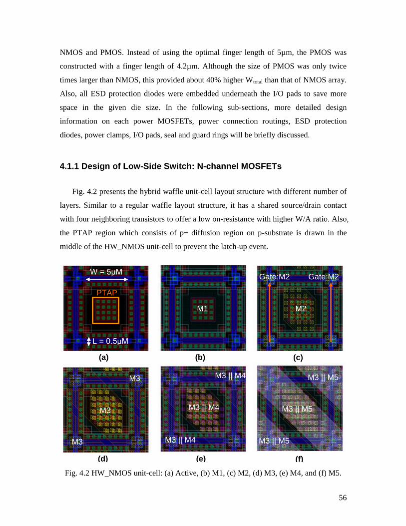
56
NMOS and PMOS. Instead of using the optimal finger length of 5µm, the PMOS was
constructed with a finger length of 4.2µm. Although the size of PMOS was only twice
times larger than NMOS, this provided about 40% higher Wtotal than that of NMOS array.
Also, all ESD protection diodes were embedded underneath the I/O pads to save more
space in the given die size. In the following sub-sections, more detailed design
information on each power MOSFETs, power connection routings, ESD protection
diodes, power clamps, I/O pads, seal and guard rings will be briefly discussed.
4.1.1 Design of Low-Side Switch: N-channel MOSFETs
Fig. 4.2 presents the hybrid waffle unit-cell layout structure with different number of
layers. Similar to a regular waffle layout structure, it has a shared source/drain contact
with four neighboring transistors to offer a low on-resistance with higher W/A ratio. Also,
the PTAP region which consists of p+ diffusion region on p-substrate is drawn in the
middle of the HW_NMOS unit-cell to prevent the latch-up event.
Fig. 4.2 HW_NMOS unit-cell: (a) Active, (b) M1, (c) M2, (d) M3, (e) M4, and (f) M5.
PTAP
W = 5μM
M1 M2
Gate:M2 Gate:M2
L = 0.5μM
(a) (b) (c)
M3
M3
M3 || M4 M3 || M5
M3 || M4
(f)
M3 || M5
(e) (d)
M3 || M4 M3 || M5 M3
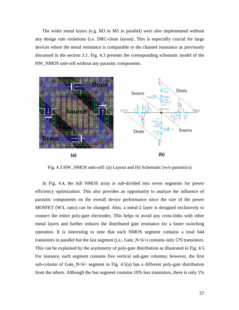
57
The wider metal layers (e.g. M3 to M5 in parallel) were also implemented without
any design rule violations (i.e. DRC-clean layout). This is especially crucial for large
devices where the metal resistance is comparable to the channel resistance as previously
discussed in the section 3.1. Fig. 4.3 presents the corresponding schematic model of the
HW_NMOS unit-cell without any parasitic components.
Fig. 4.3 HW_NMOS unit-cell: (a) Layout and (b) Schematic (w/o parasitics)
In Fig. 4.4, the full NMOS array is sub-divided into seven segments for power
efficiency optimization. This also provides an opportunity to analyze the influence of
parasitic components on the overall device performance since the size of the power
MOSFET (W/L ratio) can be changed. Also, a metal-2 layer is designed exclusively to
connect the entire poly-gate electrodes. This helps to avoid any cross-links with other
metal layers and further reduces the distributed gate resistance for a faster switching
operation. It is interesting to note that each NMOS segment contains a total 644
transistors in parallel but the last segment (i.e., Gate_N<6>) contains only 579 transistors.
This can be explained by the asymmetry of poly-gate distribution as illustrated in Fig. 4.5.
For instance, each segment contains five vertical sub-gate columns; however, the first
sub-column of Gate_N<6> segment in Fig. 4.5(a) has a different poly-gate distribution
from the others. Although the last segment contains 10% less transistors, there is only 1%
Drain
Source
Drain
(b) (a)
Source
Source
Drain
Drain
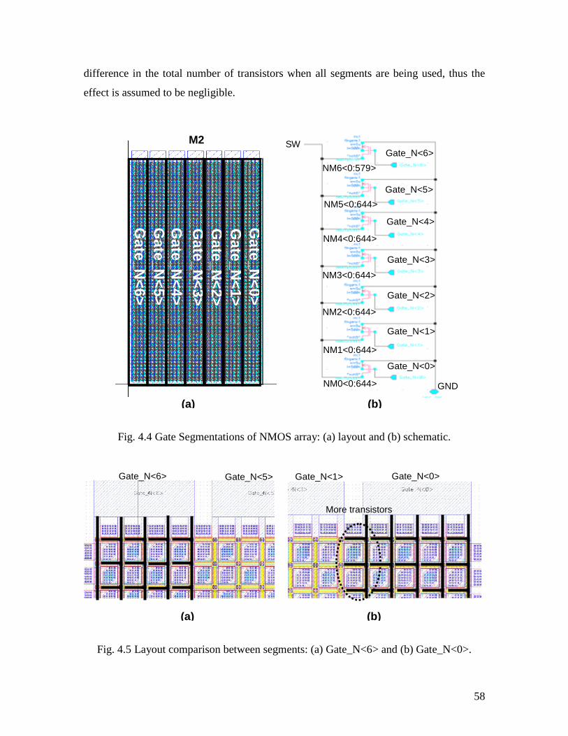
58
difference in the total number of transistors when all segments are being used, thus the
effect is assumed to be negligible.
Fig. 4.4 Gate Segmentations of NMOS array: (a) layout and (b) schematic.
Fig. 4.5 Layout comparison between segments: (a) Gate_N<6> and (b) Gate_N<0>.
(a) (b)
Gate_N<6> Gate_N<5> Gate_N<1> Gate_N<0>
More transistors
(a) (b)
Gate
_N
<6
>
Gate
_N
<5
>
Gate
_N
<4
>
Gate
_N
<3
>
Gate
_N
<2
>
Gate
_N
<1
>
Gate
_N
<0
>
M2 Gate_N<6>
Gate_N<5>
NM6<0:579>
NM5<0:644>
NM4<0:644>
NM3<0:644>
NM2<0:644>
NM1<0:644>
NM0<0:644>
Gate_N<4>
Gate_N<3>
Gate_N<2>
Gate_N<1>
Gate_N<0>
SW
GND
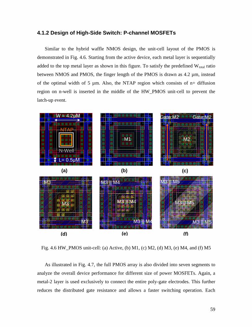
59
4.1.2 Design of High-Side Switch: P-channel MOSFETs
Similar to the hybrid waffle NMOS design, the unit-cell layout of the PMOS is
demonstrated in Fig. 4.6. Starting from the active device, each metal layer is sequentially
added to the top metal layer as shown in this figure. To satisfy the predefined Wtotal ratio
between NMOS and PMOS, the finger length of the PMOS is drawn as 4.2 µm, instead
of the optimal width of 5 µm. Also, the NTAP region which consists of n+ diffusion
region on n-well is inserted in the middle of the HW_PMOS unit-cell to prevent the
latch-up event.
Fig. 4.6 HW_PMOS unit-cell: (a) Active, (b) M1, (c) M2, (d) M3, (e) M4, and (f) M5
As illustrated in Fig. 4.7, the full PMOS array is also divided into seven segments to
analyze the overall device performance for different size of power MOSFETs. Again, a
metal-2 layer is used exclusively to connect the entire poly-gate electrodes. This further
reduces the distributed gate resistance and allows a faster switching operation. Each
(a) (b) (c)
M3
M3
M3 || M4 M3 || M5
M3 || M4
(f) (e) (d)
M3 || M4 M3 || M5 M3
W = 4.2μM
L= 0.5μM
N-Well
NTAP
Gate:M2 Gate:M2
M1 M2
M3 || M5
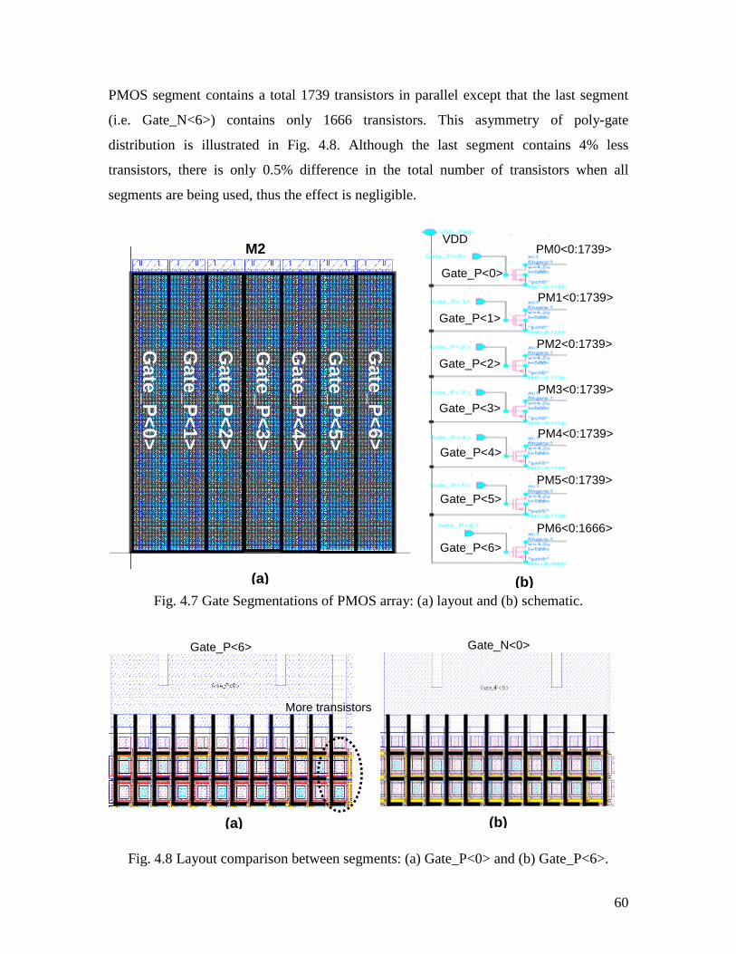
60
PMOS segment contains a total 1739 transistors in parallel except that the last segment
(i.e. Gate_N<6>) contains only 1666 transistors. This asymmetry of poly-gate
distribution is illustrated in Fig. 4.8. Although the last segment contains 4% less
transistors, there is only 0.5% difference in the total number of transistors when all
segments are being used, thus the effect is negligible.
Fig. 4.7 Gate Segmentations of PMOS array: (a) layout and (b) schematic.
Fig. 4.8 Layout comparison between segments: (a) Gate_P<0> and (b) Gate_P<6>.
(a) (b)
More transistors
Gate_P<6> Gate_N<0>
(a) (b)
M2
Gate
_P
<0
>
Gate
_P
<1
>
Gate
_P
<2
>
Gate
_P
<3
>
Gate
_P
<4
>
Gate
_P
<5
>
Gate
_P
<6
>
Gate_P<0>
Gate_P<1>
PM0<0:1739>
PM1<0:1739>
PM2<0:1739>
PM3<0:1739>
PM4<0:1739>
PM5<0:1739>
PM6<0:1666>
Gate_P<2>
Gate_P<3>
Gate_P<4>
Gate_P<5>
Gate_P<6>
VDD
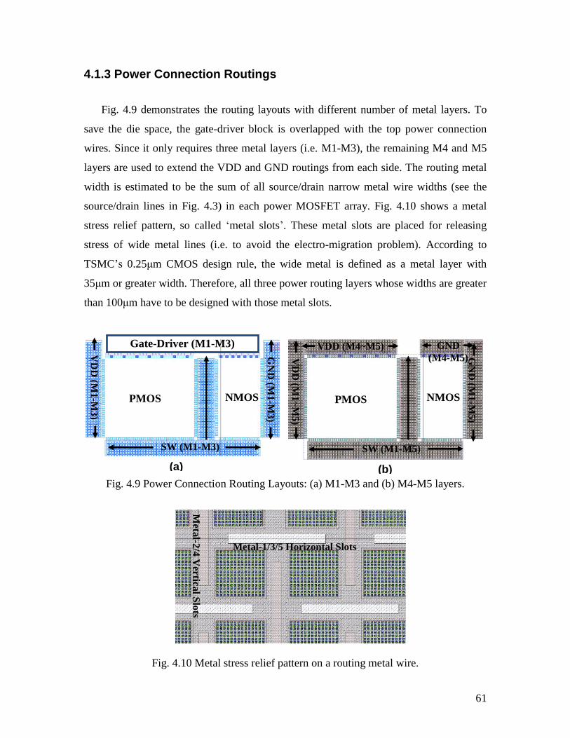
61
4.1.3 Power Connection Routings
Fig. 4.9 demonstrates the routing layouts with different number of metal layers. To
save the die space, the gate-driver block is overlapped with the top power connection
wires. Since it only requires three metal layers (i.e. M1-M3), the remaining M4 and M5
layers are used to extend the VDD and GND routings from each side. The routing metal
width is estimated to be the sum of all source/drain narrow metal wire widths (see the
source/drain lines in Fig. 4.3) in each power MOSFET array. Fig. 4.10 shows a metal
stress relief pattern, so called „metal slots‟. These metal slots are placed for releasing
stress of wide metal lines (i.e. to avoid the electro-migration problem). According to
TSMC‟s 0.25μm CMOS design rule, the wide metal is defined as a metal layer with
35μm or greater width. Therefore, all three power routing layers whose widths are greater
than 100μm have to be designed with those metal slots.
Fig. 4.9 Power Connection Routing Layouts: (a) M1-M3 and (b) M4-M5 layers.
Fig. 4.10 Metal stress relief pattern on a routing metal wire.
Metal-1/3/5 Horizontal Slots
Meta
l-2/4
Vertica
l Slo
ts
(a) (b)
SW (M1-M3)
PMOS NMOS
GN
D (M
1-M
3)
Gate-Driver (M1-M3) VDD (M4~M5)
PMOS NMOS
GND
(M4-M5) VD
D (M
1~
M5)
SW (M1-M5)
VD
D (M
1-M
3)
GN
D (M
1-M
5)

62
4.1.4 ESD Protection, Power Clamp, and Guard Rings
ESD (Electro Static Discharge) protection circuits are required for all IC components
that are likely to experience electro static discharges to the internal circuit, such as at an
input pad, an output pad, or a power rail. Fig. 4.11 shows the ESD protection diode and
power clamp layouts. In order to satisfy the 2kV HBM (Human Body Model) and 400V
MM (Machine Model) target specifications, several different components were combined
together. There were four main instances used in this layout; (i) esd_nclamp5v_500p4U,
(ii) resistor_172k, (iii) pad_io_100×100, and (iv) pad_o_100×100. More detailed
descriptions are given in the following sections.
Fig. 4.11 2kV HBM and 400 MM ESD protection circuit, (a) layout (b) schematic.
(iv)
(a)
esd_nclamp5v_500p4U
resistor_172k
pad_io_100x100
pad_o_100x100
(b)
(iii)
(ii)
(i)
VDD
GND
VDD
GND
VDD
GND
VDD
GND
VDD
GND
VDD
GND VDD
GND
Out: PT
In: DPWM_N
In: EN Out: EN
Out: DPWM_N In: DPWM_P Out: DPWM_P
In: CLK
In: SP Out: SP
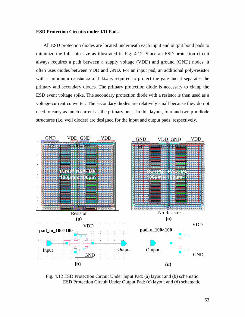
63
ESD Protection Circuits under I/O Pads
All ESD protection diodes are located underneath each input and output bond pads to
minimize the full chip size as illustrated in Fig. 4.12. Since an ESD protection circuit
always requires a path between a supply voltage (VDD) and ground (GND) nodes, it
often uses diodes between VDD and GND. For an input pad, an additional poly-resistor
with a minimum resistance of 1 kΩ is required to protect the gate and it separates the
primary and secondary diodes. The primary protection diode is necessary to clamp the
ESD event voltage spike. The secondary protection diode with a resistor is then used as a
voltage-current converter. The secondary diodes are relatively small because they do not
need to carry as much current as the primary ones. In this layout, four and two p-n diode
structures (i.e. well diodes) are designed for the input and output pads, respectively.
Fig. 4.12 ESD Protection Circuit Under Input Pad: (a) layout and (b) schematic.
ESD Protection Circuit Under Output Pad: (c) layout and (d) schematic.
Resistor
GND
VDD
M2
M1/M3/M4
INPUT PAD: M5 100μm x 100μm
VDD GND
OUTPUT PAD: M5
100μm x 100μm
No Resistor
VDD VDD GND GND
M1/M3/M4
M2
Output Input
(b)
(a) (c)
(d)
VDD
GND
Output
VDD
GND
pad_o_100×100 pad_io_100×100
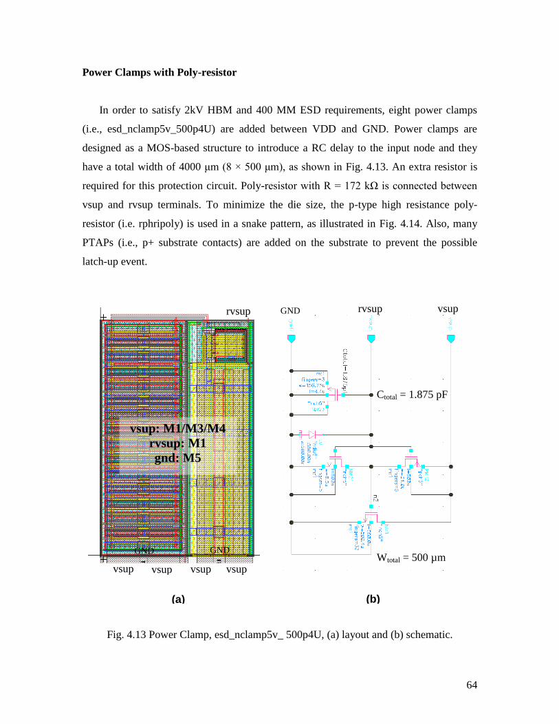
64
Power Clamps with Poly-resistor
In order to satisfy 2kV HBM and 400 MM ESD requirements, eight power clamps
(i.e., esd_nclamp5v_500p4U) are added between VDD and GND. Power clamps are
designed as a MOS-based structure to introduce a RC delay to the input node and they
have a total width of 4000 μm (8 × 500 μm), as shown in Fig. 4.13. An extra resistor is
required for this protection circuit. Poly-resistor with R = 172 kΩ is connected between
vsup and rvsup terminals. To minimize the die size, the p-type high resistance poly-
resistor (i.e. rphripoly) is used in a snake pattern, as illustrated in Fig. 4.14. Also, many
PTAPs (i.e., p+ substrate contacts) are added on the substrate to prevent the possible
latch-up event.
Fig. 4.13 Power Clamp, esd_nclamp5v_ 500p4U, (a) layout and (b) schematic.
(b) (a)
GND vsup
Ctotal = 1.875 pF
Wtotal = 500 µm
vsup: M1/M3/M4
rvsup: M1
gnd: M5
rvsup
vsup vsup vsup vsup
GND GND
rvsup

65
Fig. 4.14 p-type high resistance poly-resistor, rphripoly, (a) layout and (b) schematic.
Seal and Guard Rings
For physical stress damage and additional latch-up preventions, seal and guard rings
are employed, respectively. For instance, the seal ring is essentially a huge substrate
contact around the outside of each chip. It is basically a chunk of metal. All metal layers
in the process are stacked on top of each other, in order to keep any cracks that occur at
the edge of the die from working their way into the circuitry inside. Also, to prevent the
latch-up, a guard ring is used to surround the die (i.e., p+ in p-well and n+ in n-well).
Both seal and guard rings used in the output stage are shown in Fig. 4.15.
Fig. 4.15 Seal and guard ring layout.
Guard Ring
Seal Ring
(b) (a)
vsup
GND
rvsup
rvsup
vsup
p-type polysilicon
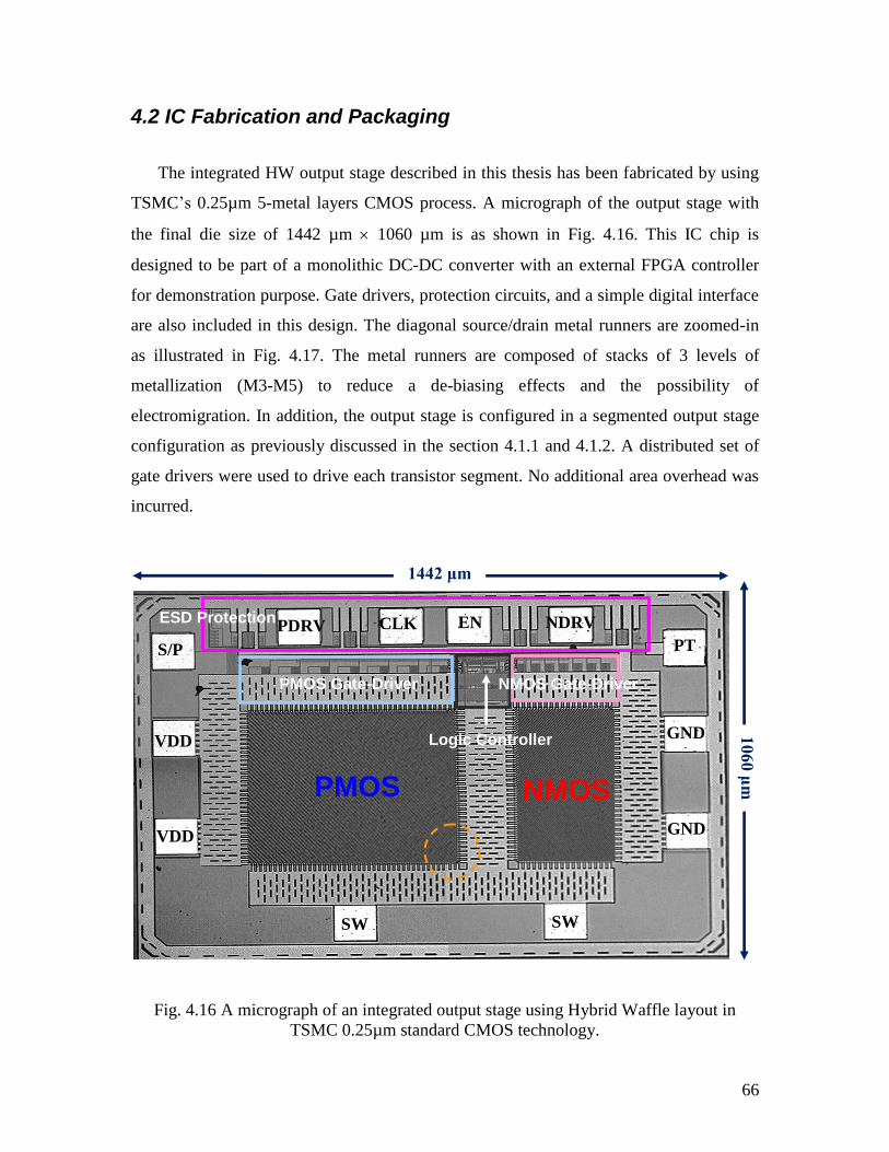
66
4.2 IC Fabrication and Packaging
The integrated HW output stage described in this thesis has been fabricated by using
TSMC‟s 0.25µm 5-metal layers CMOS process. A micrograph of the output stage with
the final die size of 1442 µm 1060 µm is as shown in Fig. 4.16. This IC chip is
designed to be part of a monolithic DC-DC converter with an external FPGA controller
for demonstration purpose. Gate drivers, protection circuits, and a simple digital interface
are also included in this design. The diagonal source/drain metal runners are zoomed-in
as illustrated in Fig. 4.17. The metal runners are composed of stacks of 3 levels of
metallization (M3-M5) to reduce a de-biasing effects and the possibility of
electromigration. In addition, the output stage is configured in a segmented output stage
configuration as previously discussed in the section 4.1.1 and 4.1.2. A distributed set of
gate drivers were used to drive each transistor segment. No additional area overhead was
incurred.
Fig. 4.16 A micrograph of an integrated output stage using Hybrid Waffle layout in
TSMC 0.25µm standard CMOS technology.
PMOS NMOS
SW
VDD GND
S/P
PDRV CLK EN NDRV
PT
GND
SW
VDD
1442 μm
Logic Controller
PMOS Gate-Driver NMOS Gate-Driver
ESD Protection
1060 μm
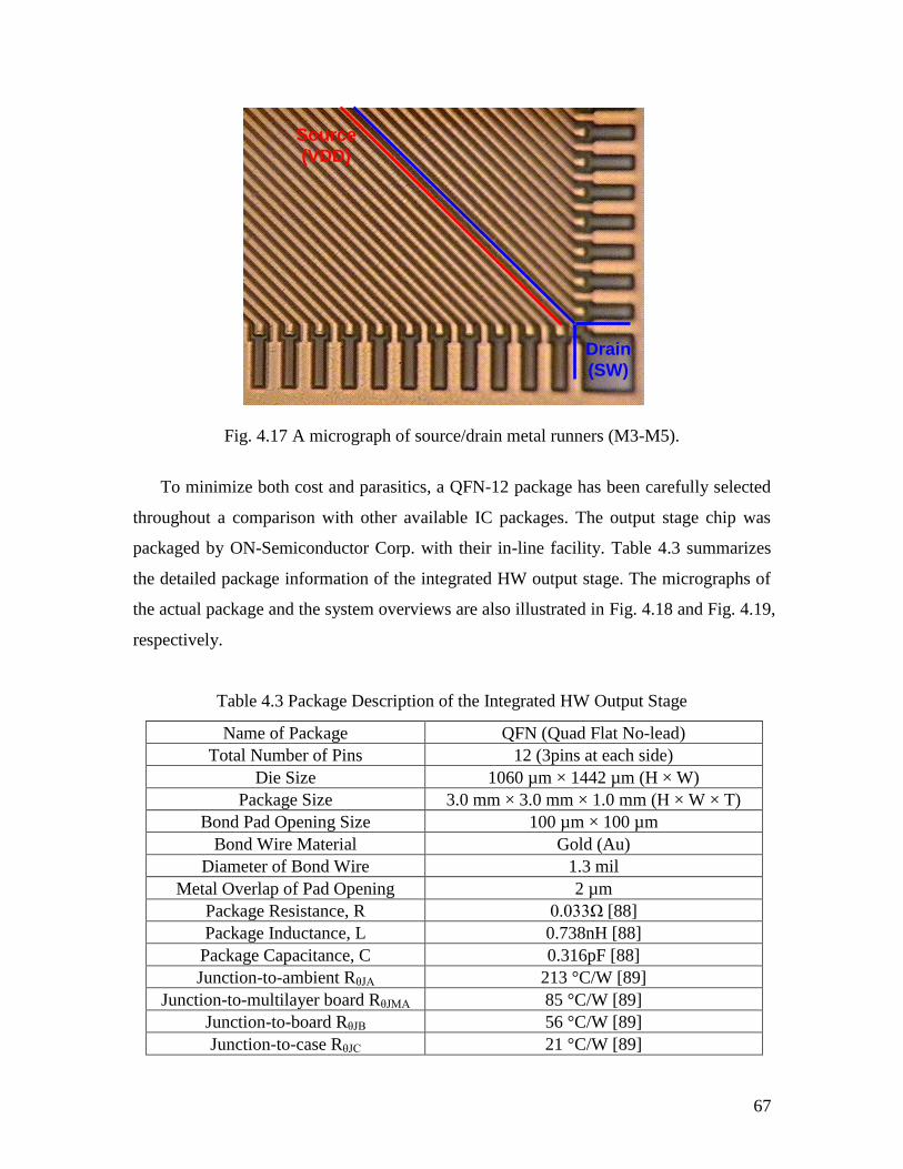
67
Fig. 4.17 A micrograph of source/drain metal runners (M3-M5).
To minimize both cost and parasitics, a QFN-12 package has been carefully selected
throughout a comparison with other available IC packages. The output stage chip was
packaged by ON-Semiconductor Corp. with their in-line facility. Table 4.3 summarizes
the detailed package information of the integrated HW output stage. The micrographs of
the actual package and the system overviews are also illustrated in Fig. 4.18 and Fig. 4.19,
respectively.
Table 4.3 Package Description of the Integrated HW Output Stage
Name of Package QFN (Quad Flat No-lead)
Total Number of Pins 12 (3pins at each side)
Die Size 1060 µm × 1442 µm (H × W)
Package Size 3.0 mm × 3.0 mm × 1.0 mm (H × W × T)
Bond Pad Opening Size 100 µm × 100 µm
Bond Wire Material Gold (Au)
Diameter of Bond Wire 1.3 mil
Metal Overlap of Pad Opening 2 µm
Package Resistance, R 0.033Ω [88]
Package Inductance, L 0.738nH [88]
Package Capacitance, C 0.316pF [88]
Junction-to-ambient RθJA 213 °C/W [89]
Junction-to-multilayer board RθJMA 85 °C/W [89]
Junction-to-board RθJB 56 °C/W [89]
Junction-to-case RθJC 21 °C/W [89]
Source
(VDD)
Drain
(SW)
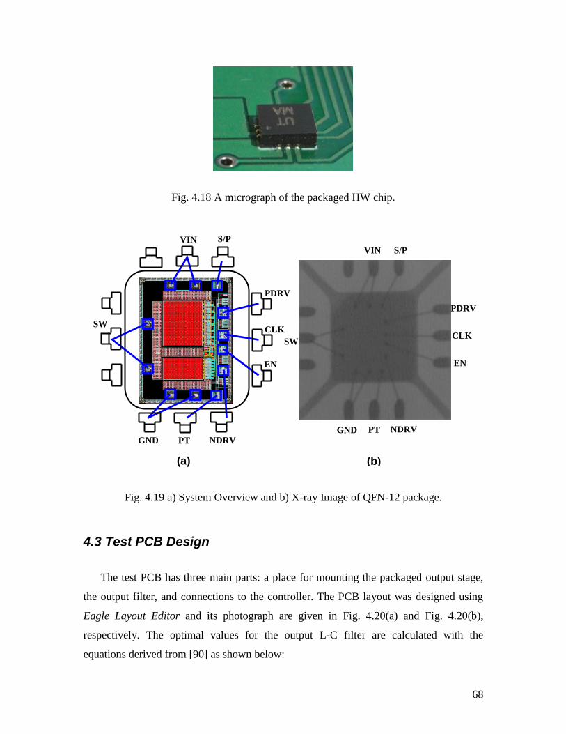
68
Fig. 4.18 A micrograph of the packaged HW chip.
Fig. 4.19 a) System Overview and b) X-ray Image of QFN-12 package.
4.3 Test PCB Design
The test PCB has three main parts: a place for mounting the packaged output stage,
the output filter, and connections to the controller. The PCB layout was designed using
Eagle Layout Editor and its photograph are given in Fig. 4.20(a) and Fig. 4.20(b),
respectively. The optimal values for the output L-C filter are calculated with the
equations derived from [90] as shown below:
SW
VIN S/P
PDRV
CLK
EN
NDRV PT GND
SW
VIN S/P
CLK
EN
NDRV PT GND
(b) (a)
PDRV

69
SL
outinf
fi
DVVL
2
)( (Eq.4.1)
SC
Lf
fv
iC
8 (Eq.4.2)
where Li is a load current variation and Cv is a tolerance of output voltage.
To control the output stage, an Altera Cyclone III FPGA development kit is used. The
controller code programmed into Cyclone III is scripted by Marian Chang. The
programmable electronic load, HP6051A, is connected to the output of the L-C filter as a
load for the output stage with current ranging from 10 to 800 mA. Standard lab
equipments are employed for power supply, and measurements of voltage and current.
Fig. 4.20 Test PCB: (a) layout (silkscreen-view) and (b) photograph.
Connectors to FPGA
Output
Filter
ADC
Transceivers
LDOs
(a) (b)
Output Stage

70
4.4 Experimental Results and Discussion
4.4.1 On-Resistance Measurements
The overall resistances of the n- and p-type HW power MOSFETs were measured
with one to seven parallel segments by using a combination of HP E3631A DC Power
Supply and Agilent 3441A Digital Multi-meter. The test circuits for on-resistance
measurements for both the high-side and the low-side power MOSFETs are as shown in
Fig. 4.21. By attaching an external resistor to each test circuit, the on-resistances were
able to be measured. For NMOS, the Ron calculation method is following as:
extswx
sw
ds
swON(LS)
)/RV(V
V
I
VR
(Eq.4.3)
For PMOS,
extsw
swsup
ds
swsup
ON(HS)/RV
)V(V
I
)V(VR
(Eq.4.4)
From these two equations, several Ron measurements for different number of each
PMOS and NMOS segments are calculated and the data are summarized in Table 4.4.
Fig. 4.21 Test circuits for on-resistance measurements: (a) NMOS and (b) PMOS
VIN
+ -
VX
On
Off REXT
VSW
VGND
VSUP
Off
On
REXT
VSW
VGND
(b) (a)

71
Table 4.4 Summary of on-resistance measurements.
NMOS: QFN-12 PMOS: QFN-12
# of Segment = 1 # of Segment = 1
VIN (V) 2.5 3.3 5.0 VIN (V) 2.5 3.3 5.0
REXT (Ω) 19.25 19.25 19.25 REXT (Ω) 19.25 19.25 19.25
IDS (A) 0.098 0.099 0.100 IDS (A) 0.126 0.152 0.226
VX (V) 1.999 1.998 1.998 VX (V) 2.667 3.164 4.614
VSW (V) 0.111 0.086 0.066 VSW (V) 2.427 2.920 4.348
VGND (V) 0 0 0 VGND (V) 0 0 0
RON (Ω) 1.134 0.870 0.662 RON (Ω) 1.904 1.609 1.178
Ratio 4.85 4.38 3.91 Ratio 5.29 5.21 4.51
# of Segment = 2 # of Segment = 2
VIN (V) 2.5 3.3 5.0 VIN (V) 2.5 3.3 5.0
REXT (Ω) 19.25 19.25 19.25 REXT (Ω) 19.25 19.25 19.25
IDS (A) 0.101 0.101 0.102 IDS (A) 0.129 0.155 0.231
VX (V) 1.998 1.998 1.998 VX (V) 2.611 3.108 4.601
VSW (V) 0.060 0.048 0.038 VSW (V) 2.483 2.977 4.445
VGND (V) 0 0 0 VGND (V) 0 0 0
RON (Ω) 0.601 0.476 0.374 RON (Ω) 0.992 0.847 0.676
Ratio 2.57 2.40 2.21 Ratio 2.76 2.74 2.59
# of Segment = 3 # of Segment = 3
VIN (V) 2.5 3.3 5.0 VIN (V) 2.5 3.3 5.0
REXT (Ω) 19.25 19.25 19.25 REXT (Ω) 19.25 19.25 19.25
IDS (A) 0.102 0.102 0.102 IDS (A) 0.133 0.158 0.230
VX (V) 1.998 1.998 1.998 VX (V) 2.641 3.138 4.530
VSW (V) 0.043 0.034 0.028 VSW (V) 2.551 3.047 4.428
VGND (V) 0 0 0 VGND (V) 0 0 0
RON (Ω) 0.424 0.336 0.275 RON (Ω) 0.679 0.575 0.443
Ratio 1.82 1.69 1.62 Ratio 1.89 1.86 1.70
# of Segment = 4 # of Segment = 4
VIN (V) 2.5 3.3 5.0 VIN (V) 2.5 3.3 5.0
REXT (Ω) 19.25 19.25 19.25 REXT (Ω) 19.25 19.25 19.25
IDS (A) 0.102 0.102 0.103 IDS (A) 0.133 0.159 0.235
VX (V) 1.998 1.998 1.998 VX (V) 2.630 3.124 4.615
VSW (V) 0.035 0.029 0.024 VSW (V) 2.558 3.054 4.531
VGND (V) 0 0 0 VGND (V) 0 0 0
RON (Ω) 0.344 0.282 0.230 RON (Ω) 0.542 0.441 0.357
Ratio 1.47 1.42 1.36 Ratio 1.51 1.43 1.37

72
# of Segment = 5 # of Segment = 5
VIN (V) 2.5 3.3 5.0 VIN (V) 2.5 3.3 5.0
REXT (Ω) 19.25 19.25 19.25 REXT (Ω) 19.25 19.25 19.25
IDS (A) 0.102 0.102 0.103 IDS (A) 0.131 0.161 0.235
VX (V) 1.998 1.998 1.998 VX (V) 2.576 3.170 4.603
VSW (V) 0.031 0.026 0.021 VSW (V) 2.515 3.107 4.530
VGND (V) 0 0 0 VGND (V) 0 0 0
RON (Ω) 0.299 0.249 0.207 RON (Ω) 0.467 0.390 0.310
Ratio 1.28 1.25 1.23 Ratio 1.30 1.26 1.19
# of Segment = 6 # of Segment = 6
VIN (V) 2.5 3.3 5.0 VIN (V) 2.5 3.3 5.0
REXT (Ω) 19.25 19.25 19.25 REXT (Ω) 19.25 19.25 19.25
IDS (A) 0.102 0.103 0.103 IDS (A) 0.128 0.162 0.228
VX (V) 1.998 1.998 1.998 VX (V) 2.521 3.167 4.461
VSW (V) 0.027 0.023 0.019 VSW (V) 2.468 3.111 4.397
VGND (V) 0 0 0 VGND (V) 0 0 0
RON (Ω) 0.264 0.223 0.188 RON (Ω) 0.415 0.347 0.280
Ratio 1.13 1.12 1.11 Ratio 1.15 1.12 1.07
# of Segment = 7 # of Segment = 7
VIN (V) 2.5 3.3 5.0 VIN (V) 2.5 3.3 5.0
REXT (Ω) 19.25 19.25 19.25 REXT (Ω) 19.25 19.25 19.25
IDS (A) 0.103 0.103 0.103 IDS (A) 0.128 0.162 0.234
VX (V) 1.999 1.999 1.999 VX (V) 2.518 3.168 4.558
VSW (V) 0.024 0.020 0.017 VSW (V) 2.472 3.118 4.497
VGND (V) 0 0 0 VGND (V) 0 0 0
RON (Ω) 0.234 0.199 0.169 RON (Ω) 0.360 0.309 0.261
Ratio 1.00 1.00 1.00 Ratio 1.00 1.00 1.00
The Ron measurements for three different voltage ratings are plotted in Fig. 4.22. The
overall on-resistance for each NMOS and PMOS is found to be decreased as the number
of segments in the output stage is increased. Since the higher number of segments refers
to the higher number of HW unit cells or the larger power MOSFET area, these results
confirm the functionality of the on-chip segmentation control logics.
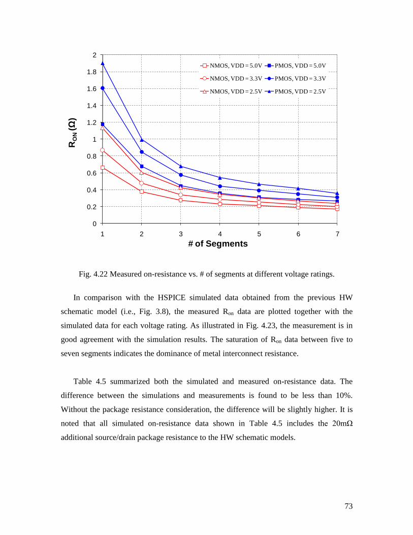
73
Fig. 4.22 Measured on-resistance vs. # of segments at different voltage ratings.
In comparison with the HSPICE simulated data obtained from the previous HW
schematic model (i.e., Fig. 3.8), the measured Ron data are plotted together with the
simulated data for each voltage rating. As illustrated in Fig. 4.23, the measurement is in
good agreement with the simulation results. The saturation of Ron data between five to
seven segments indicates the dominance of metal interconnect resistance.
Table 4.5 summarized both the simulated and measured on-resistance data. The
difference between the simulations and measurements is found to be less than 10%.
Without the package resistance consideration, the difference will be slightly higher. It is
noted that all simulated on-resistance data shown in Table 4.5 includes the 20mΩ
additional source/drain package resistance to the HW schematic models.
0
0.2
0.4
0.6
0.8
1
1.2
1.4
1.6
1.8
2
1 2 3 4 5 6 7
RO
N(Ω
)
# of Segments
NMOS, VDD = 5.0V PMOS, VDD = 5.0V
NMOS, VDD = 3.3V PMOS, VDD = 3.3V
NMOS, VDD = 2.5V PMOS, VDD = 2.5V
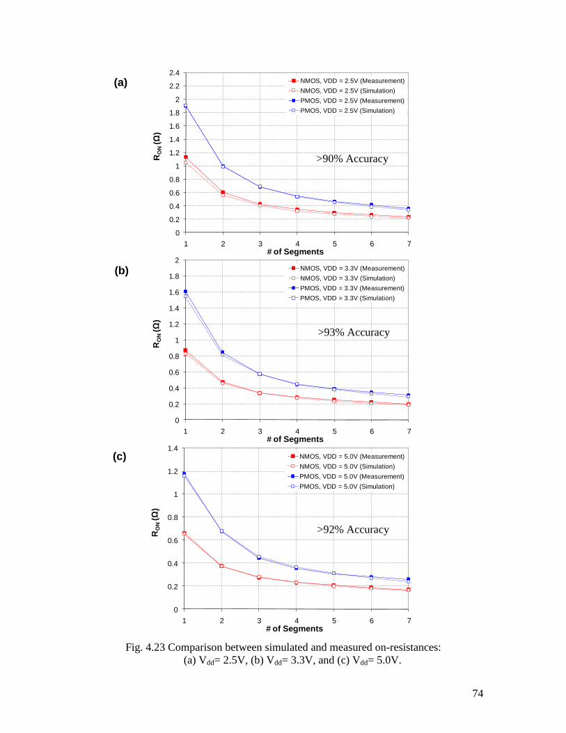
74
Fig. 4.23 Comparison between simulated and measured on-resistances:
(a) Vdd= 2.5V, (b) Vdd= 3.3V, and (c) Vdd= 5.0V.
(a)
(b)
(c)
0
0.2
0.4
0.6
0.8
1
1.2
1.4
1 2 3 4 5 6 7
RO
N(Ω
)
# of Segments
NMOS, VDD = 5.0V (Measurement)
NMOS, VDD = 5.0V (Simulation)
PMOS, VDD = 5.0V (Measurement)
PMOS, VDD = 5.0V (Simulation)
0
0.2
0.4
0.6
0.8
1
1.2
1.4
1.6
1.8
2
1 2 3 4 5 6 7
RO
N(Ω
)
# of Segments
NMOS, VDD = 3.3V (Measurement)
NMOS, VDD = 3.3V (Simulation)
PMOS, VDD = 3.3V (Measurement)
PMOS, VDD = 3.3V (Simulation)
0
0.2
0.4
0.6
0.8
1
1.2
1.4
1.6
1.8
2
2.2
2.4
1 2 3 4 5 6 7
RO
N(Ω
)
# of Segments
NMOS, VDD = 2.5V (Measurement)
NMOS, VDD = 2.5V (Simulation)
PMOS, VDD = 2.5V (Measurement)
PMOS, VDD = 2.5V (Simulation)
>92% Accuracy
>93% Accuracy
>90% Accuracy

75
Table 4.5 Data comparison between simulated and measured on-resistances.
NMOS RON @ VIN = 2.5V RON @ VIN = 3.3V RON @ VIN = 5.0V
# of Segments Meas.
(V)
Sim.
(V)
Error
(%)
Meas.
(V)
Sim.
(V)
Error
(%)
Meas.
(V)
Sim.
(V)
Error
(%)
1 1.134 1.048 7.6 0.870 0.829 4.8 0.662 0.655 1.0
2 0.601 0.559 7.0 0.476 0.458 3.9 0.374 0.375 0.2
3 0.424 0.401 5.6 0.336 0.335 0.4 0.275 0.281 2.2
4 0.344 0.321 6.5 0.282 0.273 3.2 0.230 0.232 1.0
5 0.299 0.273 8.8 0.249 0.234 6.3 0.207 0.201 2.9
6 0.264 0.239 9.4 0.223 0.207 7.2 0.188 0.179 4.8
7 0.234 0.216 7.7 0.199 0.188 5.6 0.169 0.164 3.1
PMOS RON @ VIN = 2.5V RON @ VIN = 3.3V RON @ VIN = 5.0V
# of Segments Meas.
(V)
Sim.
(V)
Error
(%)
Meas.
(V)
Sim.
(V)
Error
(%)
Meas.
(V)
Sim.
(V)
Error
(%)
1 1.904 1.909 0.3 1.609 1.545 4.0 1.178 1.161 1.4
2 0.992 0.984 0.8 0.847 0.812 4.1 0.676 0.678 0.4
3 0.679 0.688 1.3 0.575 0.576 0.2 0.443 0.455 2.6
4 0.542 0.541 0.2 0.441 0.449 1.7 0.357 0.367 2.8
5 0.487 0.449 3.8 0.390 0.379 3.0 0.310 0.311 0.2
6 0.415 0.386 6.9 0.347 0.331 4.5 0.280 0.271 3.4
7 0.360 0.338 6.1 0.309 0.288 6.7 0.261 0.239 8.4
4.4.2 Gate-drive Loss Measurements
The total input gate charge measurement is also desirable to analyze the trade-off
relationship between Ron and Qg in a segmented output stage. However, Qg was not able
to be measured directly because there was no test point at the gate terminals of the power
MOSFETs. Therefore, the gate-drive loss, Pgate which is proportional to Qg, was
measured instead as part of the total dynamic power consumption, Pdyn. As shown in Fig.
4.24, the total Pdyn was measured during switching includes the gate-drive loss, diode
conduction and reverse recovery loss, switching loss, shoot-through loss, and power
consumed by the protection circuits and level-shifters in the switching mode [91-92].
Since the measurements are taken by setting the load current to zero, the diode and
switching losses which are proportional to the load current are approximately zero.
Moreover, the gate-drive loss should be theoretically zero when no segment is enabled.

76
However, there was a minimum power consumption of approximately 10 mW at no
segment. In order to extract the true Pgate, the dynamic losses of the level-shifter and over-
current protection circuits were subtracted from the total Pdyn. The Pgate data for different
number of segments are summarized in Table 4.6. By considering the Wtotal ratio between
NMOS and PMOS, the Pgate data for different number of each NMOS and PMOS
segments could be estimated from the measured total Pgate.
Fig. 4.24 Total dynamic and gate-drive power measurements.
Table 4.6 Summary of Gate-Drive Power Calculated from Measurements
# of Segments 1 2 3 4 5 6 7
Pgate-Total (mW) 1.89 4.08 5.83 8.45 9.81 12.19 13.38
Pgate-PMOS (mW) 1.32 2.85 4.08 5.91 6.86 8.53 9.36
Pgate-NMOS (mW) 0.57 1.23 1.75 2.54 2.95 3.66 4.02
Ratio to 1-segment 1.0 2.2 3.1 4.5 5.2 6.5 7.1
0
5
10
15
20
25
0 1 2 3 4 5 6 7 8
Po
wer
(mW
)
# of Segments
Pdyn_total
Pgate_total
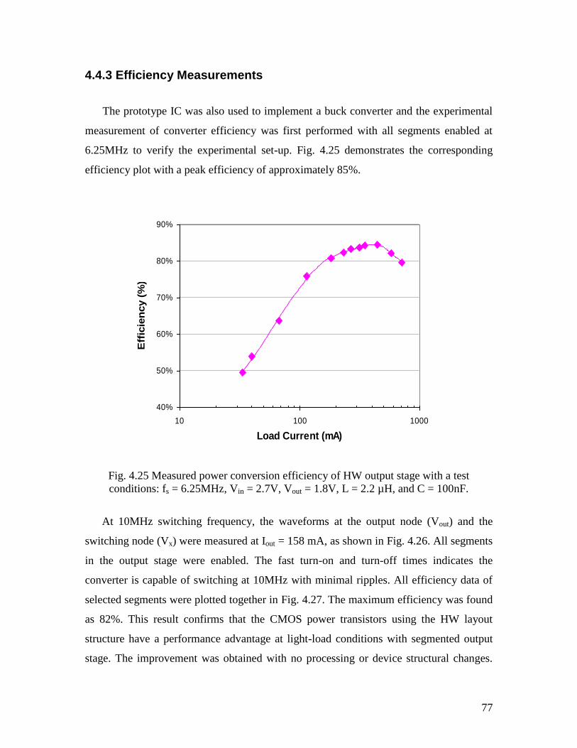
77
4.4.3 Efficiency Measurements
The prototype IC was also used to implement a buck converter and the experimental
measurement of converter efficiency was first performed with all segments enabled at
6.25MHz to verify the experimental set-up. Fig. 4.25 demonstrates the corresponding
efficiency plot with a peak efficiency of approximately 85%.
Fig. 4.25 Measured power conversion efficiency of HW output stage with a test
conditions: fs = 6.25MHz, Vin = 2.7V, Vout = 1.8V, L = 2.2 µH, and C = 100nF.
At 10MHz switching frequency, the waveforms at the output node (Vout) and the
switching node (Vx) were measured at Iout = 158 mA, as shown in Fig. 4.26. All segments
in the output stage were enabled. The fast turn-on and turn-off times indicates the
converter is capable of switching at 10MHz with minimal ripples. All efficiency data of
selected segments were plotted together in Fig. 4.27. The maximum efficiency was found
as 82%. This result confirms that the CMOS power transistors using the HW layout
structure have a performance advantage at light-load conditions with segmented output
stage. The improvement was obtained with no processing or device structural changes.
40%
50%
60%
70%
80%
90%
10 100 1000
Load Current (mA)
Eff
icie
ncy (
%)
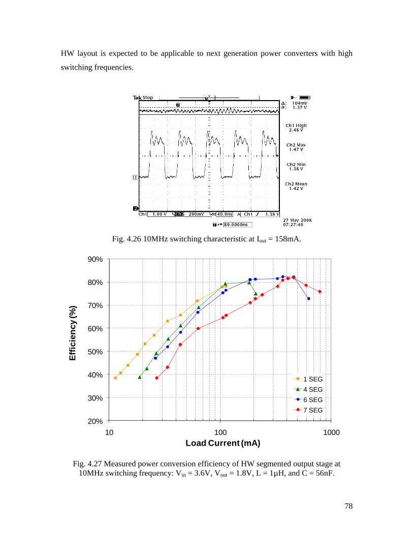
78
HW layout is expected to be applicable to next generation power converters with high
switching frequencies.
Fig. 4.26 10MHz switching characteristic at Iout = 158mA.
Fig. 4.27 Measured power conversion efficiency of HW segmented output stage at
10MHz switching frequency: Vin = 3.6V, Vout = 1.8V, L = 1µH, and C = 56nF.
20%
30%
40%
50%
60%
70%
80%
90%
10 100 1000
Eff
icie
nc
y (%
)
Load Current (mA)
1 SEG
4 SEG
6 SEG
7 SEG

79
4.5 Summary
This chapter covers the HW layout technique for the design of CMOS power
transistors in a low voltage DC-DC buck converter. A prototype IC that contains
integrated gate drivers, protection circuits and CMOS output power transistors was
implemented in a standard 0.25µm CMOS process. The experimental measurements of
the on-resistance and gate-drive loss confirmed the advantages of the HW structure in a
VLSI based process, making the MOSFET a suitable candidate for on-chip, high
frequency switch mode DC-DC converters. The performance improvement was obtained
with no processing or device structural changes. The measured overall on-resistances for
both the n- and p-type power MOSFETs were in good agreement with the earlier
simulation results. Also, the segmentation of the power MOSFET array enhanced the
converter efficiency at the light-load conditions. The maximum measured efficiencies of
the converter switching at 6.25 MHz and 10MHz were 85% and 82%, respectively.
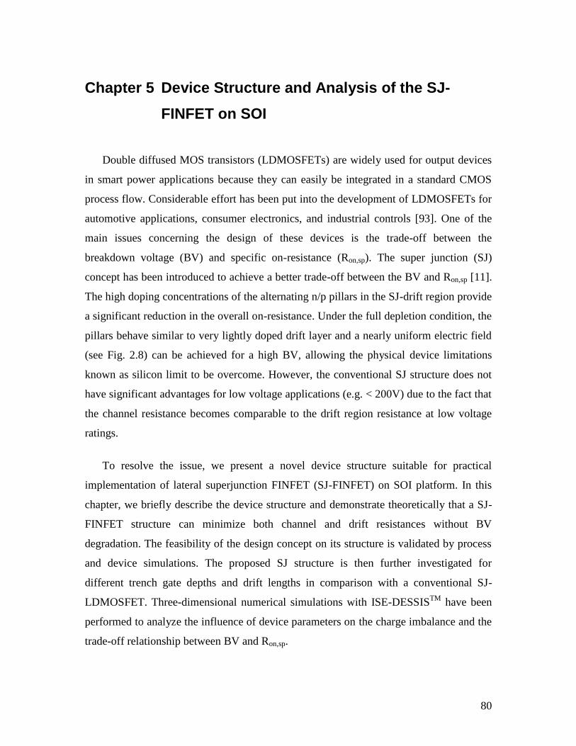
80
Chapter 5 Device Structure and Analysis of the SJ-
FINFET on SOI
Double diffused MOS transistors (LDMOSFETs) are widely used for output devices
in smart power applications because they can easily be integrated in a standard CMOS
process flow. Considerable effort has been put into the development of LDMOSFETs for
automotive applications, consumer electronics, and industrial controls [93]. One of the
main issues concerning the design of these devices is the trade-off between the
breakdown voltage (BV) and specific on-resistance (Ron,sp). The super junction (SJ)
concept has been introduced to achieve a better trade-off between the BV and Ron,sp [11].
The high doping concentrations of the alternating n/p pillars in the SJ-drift region provide
a significant reduction in the overall on-resistance. Under the full depletion condition, the
pillars behave similar to very lightly doped drift layer and a nearly uniform electric field
(see Fig. 2.8) can be achieved for a high BV, allowing the physical device limitations
known as silicon limit to be overcome. However, the conventional SJ structure does not
have significant advantages for low voltage applications (e.g. < 200V) due to the fact that
the channel resistance becomes comparable to the drift region resistance at low voltage
ratings.
To resolve the issue, we present a novel device structure suitable for practical
implementation of lateral superjunction FINFET (SJ-FINFET) on SOI platform. In this
chapter, we briefly describe the device structure and demonstrate theoretically that a SJ-
FINFET structure can minimize both channel and drift resistances without BV
degradation. The feasibility of the design concept on its structure is validated by process
and device simulations. The proposed SJ structure is then further investigated for
different trench gate depths and drift lengths in comparison with a conventional SJ-
LDMOSFET. Three-dimensional numerical simulations with ISE-DESSISTM
have been
performed to analyze the influence of device parameters on the charge imbalance and the
trade-off relationship between BV and Ron,sp.
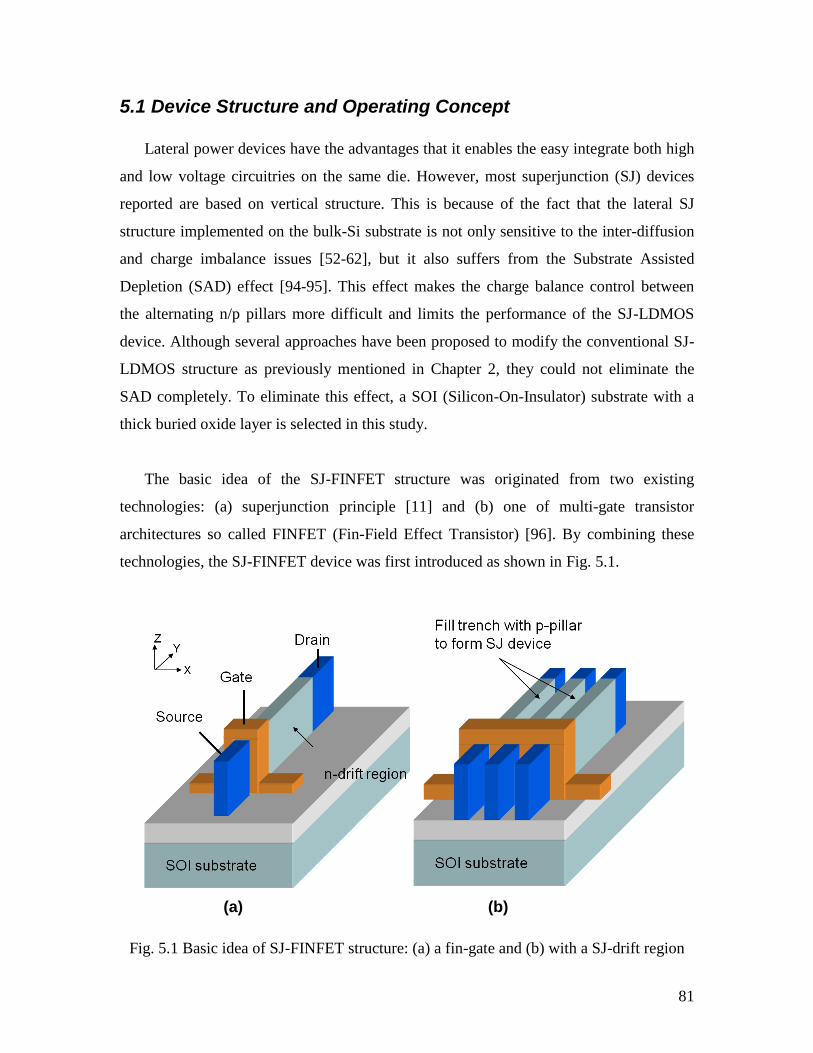
81
5.1 Device Structure and Operating Concept
Lateral power devices have the advantages that it enables the easy integrate both high
and low voltage circuitries on the same die. However, most superjunction (SJ) devices
reported are based on vertical structure. This is because of the fact that the lateral SJ
structure implemented on the bulk-Si substrate is not only sensitive to the inter-diffusion
and charge imbalance issues [52-62], but it also suffers from the Substrate Assisted
Depletion (SAD) effect [94-95]. This effect makes the charge balance control between
the alternating n/p pillars more difficult and limits the performance of the SJ-LDMOS
device. Although several approaches have been proposed to modify the conventional SJ-
LDMOS structure as previously mentioned in Chapter 2, they could not eliminate the
SAD completely. To eliminate this effect, a SOI (Silicon-On-Insulator) substrate with a
thick buried oxide layer is selected in this study.
The basic idea of the SJ-FINFET structure was originated from two existing
technologies: (a) superjunction principle [11] and (b) one of multi-gate transistor
architectures so called FINFET (Fin-Field Effect Transistor) [96]. By combining these
technologies, the SJ-FINFET device was first introduced as shown in Fig. 5.1.
Fig. 5.1 Basic idea of SJ-FINFET structure: (a) a fin-gate and (b) with a SJ-drift region
(a) (b)

82
However, one of issues within this initial structure is that it needs to fill the trench with
an epitaxial layer, whose growth technique is generally not compatible with modern
CMOS processes. Also, it has a relatively poor crystalline quality due to a higher
dislocation density. To solve this problem, several attempts have been reported by using a
doped poly-Si as an alternative [97] but the inter-diffusion is another issue because a
dopant (e.g. boron) from the as-deposited poly-Si can easily diffuse into the n-pillar or
segregate at the interface during a high temperature thermal processing step.
In general, the on-resistance of a lateral SJ structure can be reduced by increasing the
n/p-drift region doping concentrations (ND, NA), narrowing the n/p-drift region pillar
widths (WN, WP) and increasing their height (Tepi). Normally, the minimum n/p-drift
region pillar widths are limited by the processing rules. Therefore, increasing Tepi is an
effective way to reduce the on-resistance of lateral SJ structures however this should be
followed by the deep n/p pillar formations in the drift region. Since the project range (Rp)
of a high energy ion implantation can only reach up to approximately 1µm depth, a
sidewall doping of the trench by a tilted implantation is only a conventional technique to
form a deep uniform p-pillar layer without any major processing changes (i.e. CMOS-
compatibility issues).
The overview of the proposed lateral SJ-FINFET is illustrated in Fig. 5.2(a). The
proposed device structure has an embedded trench gate on the side wall and a channel on
the top surface. It is designed to increase the total channel width (i.e. Wtop + Wside) and
provide a more effective conduction path to the drift region. The cross-sections of the
proposed device structure are also demonstrated in Fig. 5.2. It can be seen that the cross-
sectional area of n-drift (Sn) is larger than that of p-drift (Sp) within the SJ unit-cell. This
asymmetric SJ drift structure are analyzed for different voltage rating in order to examine
its effect on the on-resistance and the sensitivity of the BV due to charge imbalance. To
achieve fully depleted SJ-drift region where Sn is larger than Sp, the doping concentration
of the p-drift layer (NA) should be greater than the n-drift doping concentration (ND). For
trench depths of 2 and 3 µm, NA is calculated to be about 23% and 16% greater than ND,
respectively. This indicates that the increase in NA is less pronounced for a deeper trench
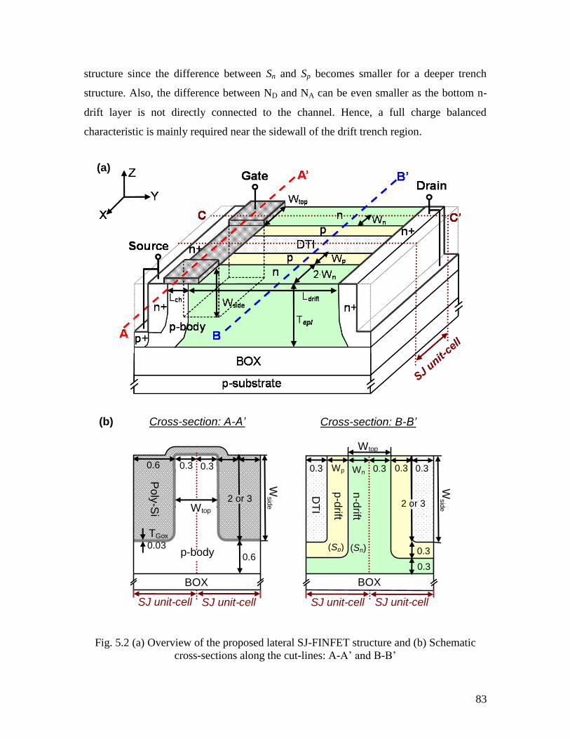
83
structure since the difference between Sn and Sp becomes smaller for a deeper trench
structure. Also, the difference between ND and NA can be even smaller as the bottom n-
drift layer is not directly connected to the channel. Hence, a full charge balanced
characteristic is mainly required near the sidewall of the drift trench region.
Fig. 5.2 (a) Overview of the proposed lateral SJ-FINFET structure and (b) Schematic
cross-sections along the cut-lines: A-A‟ and B-B‟
Cross-section: A-A’ Cross-section: B-B’
SJ unit-cell SJ unit-cell
(Sn) (Sp)
BOX
DT
I
p-d
rift
n-d
rift
Wp 0.3 Wn 0.3 0.3 0.3
0.3
0.3
2 or 3
Wtop
Wsid
e
(a)
(b)
SJ unit-cell SJ unit-cell
BOX
p-body
0.3
Wtop
Poly
-Si
0.6 0.3
0.6
Wsid
e
2 or 3
TGox 0.03
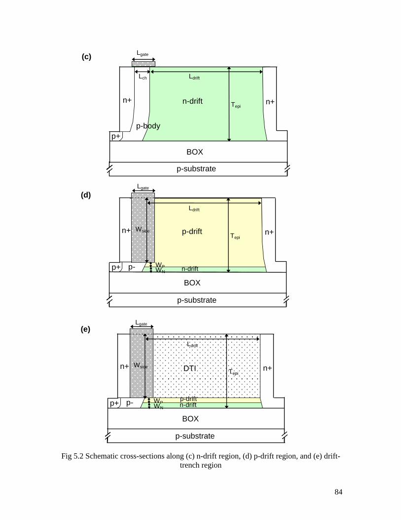
84
Fig 5.2 Schematic cross-sections along (c) n-drift region, (d) p-drift region, and (e) drift-
trench region
(c)
(d)
n+
Tepi
BOX
p-substrate
p-body
Lch Ldrift
n+ n+
p+
Lgate
n-drift
(e)
n+
Tepi
BOX
p-substrate
p-
Ldrift
n+ n+
p+
p-drift
n-drift WN WP
Lgate
Wside
n+
BOX
p-substrate
p-
n+ n+
p+ n-drift WN WP
Lgate
Wside Tepi
Ldrift
p-drift
DTI

85
The initial n-drift doping concentration for d = 0.3 µm was calculated by [11].
)cm(1041.1 36/76/712 dND (Eq.5.1)
deviceSJlateralorverticalfor1/3or1/2
where d is the width of n/p drift layer (only if pn WW d ) and is the optimal doping
coefficient (0 < < 1).
Dividing the unit-cell along the center of the structure as shown in Fig. 5.2(a), the
widths of n/p pillars within the SJ unit-cell are the same (i.e. 0.3 µm). The charge
imbalance between n-drift and p-drift layers directly affects the value of breakdown
voltage (BV). Thus, it is important to evaluate the effect of charge imbalance in order to
achieve the maximum BV. Based on the calculated ND (= 7.4 x 10¹⁶
cm3
), the charge
imbalance simulations with several NA are performed for different trench depths and drift
lengths later in the section 5.3. The ideal SJ-FINFET structure is given as a reference in
Fig. 5.3. Lastly, Table 5.1 represents the technological and geometrical parameters
considered for both process and device simulation works in this chapter.
Fig. 5.3 Ideal device structure of the proposed SJ-FINFET.

86
Table 5.1: Parameters considered for both process and device simulations
Parameter Value
Drift length, Ldrift (µm)
n-drift width, 2∙Wn (µm)
n-drift doping concentration, ND (cm-3
)
p-drift width, Wp (µm)
p-drift doping concentration, NA (cm-3
)
p-body doping concentration, Np-body (cm-3
)
p-substrate doping concentration, Nsub (cm-3
)
n+ source/drain contact, Ns/d (cm-3
)
p+ contact, Np+(cm-3
)
Gate oxide thickness, TGox (nm)
Top channel width, Wtop (µm)
Side channel width, Wside (µm)
Gate length, Lgate (µm)
Channel length, Lch (µm)
SOI thickness, Tepi (µm)
Buried oxide thickness, TBOX (µm)
3.0, 3.5, 4.0, 4.5, 5.0, 6.0, 8.0, and 12.0
0.6
7.4 × 10¹⁶
0.3
9.8, 9.2, 8.7, 8.2, 7.8, and 7.4 × 10¹⁶
5.0 × 10¹⁷
2.0 × 10¹⁴
1.0 × 10²⁰
5.0 × 10¹⁹
35
0.6
2.0 and 3.0
1.0
0.5
2.6 and 3.6
2.0

87
5.2 Process Simulations
Process simulations are performed based on 2D process simulator, TSUPREM4 [99]
to extract the specific processing conditions (e.g. dopant, does, energy, angle,
temperature, time, etch rate, gas, etc.) required for the SJ-FINFET structure. Three
important process modules such as a) P-body formation, b) SJ-drift formation, and c) N+
source/drain contact formation were mainly investigated to validate the SJ-FINFET
device concept and optimize the device parameters. The cross-sections along B-B‟ and C-
C‟ cut lines (shown in Fig. 5.2(a)) were simulated to evaluate the feasibility of those
process modules. The dose and energy of the multiple high energy ion implantations were
optimized to meet their specifications. The accurate numerical models, i.e. diffusion
model PD. TRANS, oxidation model VISCOELA and ion implantation MONTE CARLO
model were used in process steps to get more accurate process simulation results. More
detailed descriptions are given in the following sub-sections.
5.2.1 Simulation of P-body Formation
As shown in Fig. 5.2(c)-(e), the proposed SJ-FINFET structure requires an embedded
trench gate on the side wall and a channel on the top surface to provide a more effective
conduction path to the drift region. Since the minimum n/p-drift region pillar widths are
dictated by process limitations, increasing the trench gate depth (i.e., Wside) is a promising
solution to reduce the overall on-resistance. However, this requires a deep uniform P-
body formation under the gate region. In Fig. 5.4(a), the photo-mask defines the location
where the deep trench structure should be created. The reactive ion etching (i.e.
anisotropic etching) is the next process step to form the deep source/drain trench structure
with 0.6µm width and 3µm depth. In order to meet its specification (i.e. dimension), the
precise etching rate, over-etch, and time were needed for both screen oxide and Si-
substrate with a fined mesh structure. After a 45° tilted B+ ion implantation was
simulated, the photoresist was then removed prior to a thermal diffusion step. Throughout
the optimization of several different annealing conditions (i.e. temperature and duration),
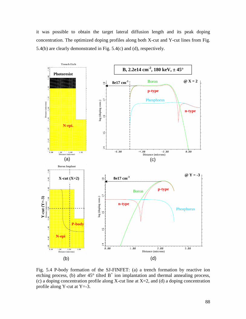
88
it was possible to obtain the target lateral diffusion length and its peak doping
concentration. The optimized doping profiles along both X-cut and Y-cut lines from Fig.
5.4(b) are clearly demonstrated in Fig. 5.4(c) and (d), respectively.
Fig. 5.4 P-body formation of the SJ-FINFET: (a) a trench formation by reactive ion
etching process, (b) after 45° tilted B+ ion implantation and thermal annealing process,
(c) a doping concentration profile along X-cut line at X=2, and (d) a doping concentration
profile along Y-cut at Y=-3.
N-epi.
p-type
B, 2.2e14 cm-2
, 180 keV, ± 45° Photoresist
(a)
(b)
(c)
(d)
Boron
Phosphorus
n-type
8e17 cm-3 @ X = 2
@ Y = -3 X-cut (X=2)
p-type Boron
Phosphorus
n-type
8e17 cm-3
N-epi
P-body
log
(d
op
ing c
on
c.)
Distance (microns)
Distance (microns)
log
(d
op
ing
co
nc.)
Boron Implant
Distance (microns)
Dis
tan
ce
(mic
ro
ns)
Distance (microns)
Dis
tan
ce
(mic
ron
s)
Y-c
ut
(Y=
-3)
Trench Etch

89
5.2.2 Simulation of SJ-drift Formation
The process simulations of the SJ-drift formation were carried out for the cross-
sections along the line B-B‟ cut line, as shown in Fig. 5.2(a), to determine the optimized
process parameters. The simulated structure for the cross-section through B-B‟ is also
given in Fig. 5.5(a)-(d). Similar to the P-body formation, a deep trench structure is
created by anisotropic dry-etching, but the silicon nitride (Si3N4) hard-mask layer was
considered instead of using the photoresist. Since the width of the drift trench limits the
device performance, a narrow deep trench structure is always preferred in the SJ-drift
region. However, this causes an issue as the sidewall doping process becomes more
difficult due to the shadowing effect [98]. To minimize this effect in a practical
implantation situation, a thin Si3N4 hard-mask layer with a thickness of 2000Å was
grown on a sacrificial oxide rather than using a relatively thick photoresist itself.
Together with the trench etch and tilted ion implantation processes, the SJ-drift
structure can be integrated on the SOI platform. By considering the aspect ratio of the
trench structure, the P-pillar formation was simulated by a 12° tilted B+ ion implantation
with maximum energy of 45 KeV and dose of 4 × 10¹³
cm-2
. After removing the Si3N4
hard-mask, it was followed by a 250-min annealing for drive-in, as shown in Fig. 5.5(e).
The doping profiles of the SJ-drift region with different implant doses were also extracted
as illustrated in Fig. 5.5(f)-(h) because the condition of exact charge balance is important
in obtaining the stable high breakdown voltage during a blocking mode. Since the width
of the alternating n/p pillars was chosen as 0.3 µm and the corresponding optimal doping
concentration (ND) was calculated as 7.4 × 10¹⁶
cm3
, as described in the section 5.1, the
doping profile of the P-pillar region in Fig. 5.5(g) demonstrates a best match. It has a
fairly uniform doping concentration with some considerably low distortion at the
junctions due to lateral diffusion and at the surface due to charge segregation into the
field oxide. It is noted that these simulation results are validated with the fabricated
devices later in Chapter 6.
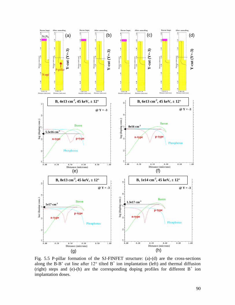
90
Fig. 5.5 P-pillar formation of the SJ-FINFET structure: (a)-(d) are the cross-sections
along the B-B‟ cut line after 12° tilted B+ ion implantation (left) and thermal diffusion
(right) steps and (e)-(h) are the corresponding doping profiles for different B+ ion
implantation doses.
Y-c
ut
(Y=
-3)
(a)
Y-c
ut
(Y=
-3)
Y-c
ut
(Y=
-3)
Y-c
ut
(Y=
-3)
(b) (c) (d)
p-type
B, 4e13 cm-2
, 45 keV, ± 12°
(e) (f)
(g) (h)
Boron
Phosphorus
n-type n-type
5.5e16 cm-3
B, 6e13 cm-2
, 45 keV, ± 12°
B, 8e13 cm-2
, 45 keV, ± 12° B, 1e14 cm-2
, 45 keV, ± 12°
p-type
Boron
Phosphorus
@ Y = -3
8e16 cm-3
@ Y = -3
1.3e17 cm-3
@ Y = -3
Boron Boron
Phosphorus Phosphorus
n-type n-type
p-type p-type
1e17 cm-3
@ Y = -3
Si3N4
N-epi
P-pillar
log
(d
op
ing
co
nc.)
log
(d
op
ing
co
nc.)
log (
do
pin
g c
on
c.)
log (
do
pin
g c
on
c.)
Distance (microns) Distance (microns)
Distance (microns) Distance (microns)
Distance (microns) Distance (microns) Distance (microns) Distance (microns) Distance (microns) Distance (microns) Distance (microns) Distance (microns)
Boron Impt. After annealing Boron Impt. Boron Impt. After annealing Boron Impt. After annealing After annealing
Dis
tan
ce (
mic
ro
ns)
Dis
tan
ce (
mic
ro
ns)
Dis
tan
ce (
mic
ro
ns)
Dis
tan
ce (
mic
ro
ns)
Dis
tan
ce (
mic
ro
ns)
Dis
tan
ce (
mic
ro
ns)
Dis
tan
ce (
mic
ro
ns)
Dis
tan
ce (
mic
ro
ns)
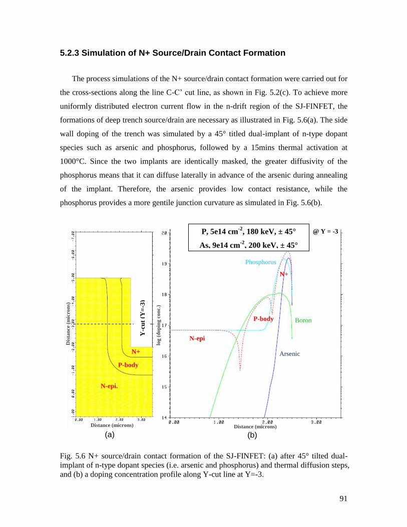
91
5.2.3 Simulation of N+ Source/Drain Contact Formation
The process simulations of the N+ source/drain contact formation were carried out for
the cross-sections along the line C-C‟ cut line, as shown in Fig. 5.2(c). To achieve more
uniformly distributed electron current flow in the n-drift region of the SJ-FINFET, the
formations of deep trench source/drain are necessary as illustrated in Fig. 5.6(a). The side
wall doping of the trench was simulated by a 45° titled dual-implant of n-type dopant
species such as arsenic and phosphorus, followed by a 15mins thermal activation at
1000°C. Since the two implants are identically masked, the greater diffusivity of the
phosphorus means that it can diffuse laterally in advance of the arsenic during annealing
of the implant. Therefore, the arsenic provides low contact resistance, while the
phosphorus provides a more gentile junction curvature as simulated in Fig. 5.6(b).
Fig. 5.6 N+ source/drain contact formation of the SJ-FINFET: (a) after 45° tilted dual-
implant of n-type dopant species (i.e. arsenic and phosphorus) and thermal diffusion steps,
and (b) a doping concentration profile along Y-cut line at Y=-3.
N-epi.
P, 5e14 cm-2
, 180 keV, ± 45°
As, 9e14 cm-2
, 200 keV, ± 45°
(b)
Y-c
ut
(Y=
-3)
P-body
N+
(a)
P-body Boron
Phosphorus
N+
@ Y = -3
Arsenic
N-epi
log
(d
op
ing c
on
c.)
Distance (microns) Distance (microns)
Dis
tan
ce (
mic
ron
s)

92
5.3 Device Simulations
After the process simulation, the full device structure and doping profile were created
by ISE-MESH and imported to ISE-DESSIS to obtain the electrical characteristics. ISE-
MESH is a three dimensional grid generation tool. The device simulator, ISE-DESSIS
accepts the three dimensional device structure exported from ISE-MESH. Various
physical and numerical models [100], e.g. Shockley-Read-Hall recombination model,
Conwell-Weisskopf model for carrier-carrier scattering, Canali model for velocity
saturation, Lombardi model for mobility degradation at interfaces, Bennet-Wilson model
for band gap and electron affinity, Overstraeten-de Man model for impact ionization and
avalanche generation model were used to get more accurate device simulation results. A
constant n-doped SOI substrate of 7.4 × 10¹⁶
cm3
with a 2um thick buried oxide layer
was considered in the simulations. A highly doped polysilicon gate was specified in ISE-
DESSIS by including a metal electrode with a barrier of -0.55 eV defined as the
difference in eV between the polysilicon Fermi level and the intrinsic Fermi level. The
detailed simulation results of the SJ-FINFET structure will be discussed in the following
sub-sections.
5.3.1 Mesh Structure and Grid Refinement
In Fig. 5.7, the unit-cell (i.e. repetitive structure) of the SJ-FINFET device is
illustrated with or without any oxide layers. The device structure was constructed by ISE-
MESH, a dimension independent and modular grid generator which generates a high-
quality spatial discretization for 3D devices. For more efficient simulations, the initial
mesh structure of the SJ-FINFET was re-fined (or re-meshed) as many times as possible
when required. It is important to note that a mesh should be created with a minimum
number of vertices to achieve a desired level of accuracy. To avoid a convergence issue,
the mesh had to be denser in some critical areas where both high current density (e.g.
channel and drift region) and high electric field (e.g. channels, drains, and depletion
regions) were expected. As shown in Fig. 5.7(b), the SJ-FINFET contains very tiny
vertical mesh spacing in the channel at the oxide interface (i.e., in order of 1Å). For the
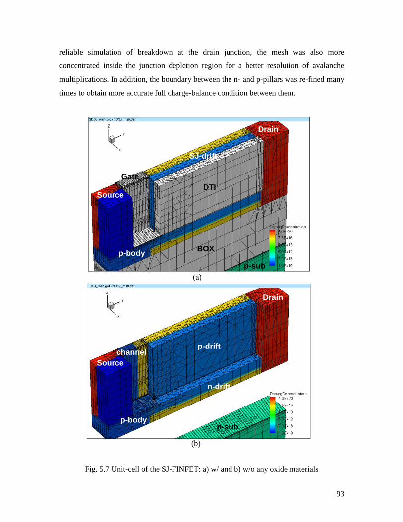
93
reliable simulation of breakdown at the drain junction, the mesh was also more
concentrated inside the junction depletion region for a better resolution of avalanche
multiplications. In addition, the boundary between the n- and p-pillars was re-fined many
times to obtain more accurate full charge-balance condition between them.
Fig. 5.7 Unit-cell of the SJ-FINFET: a) w/ and b) w/o any oxide materials
(a)
(b)
BOX p-body
SJ-drift
Drain
Source DTI
Gate
p-sub
p-sub
p-drift
n-drift
channel
Source
p-body
Drain

94
5.3.2 Off-State Simulations
The simulated SJ-FINFET device had several different drift region lengths with a
trench gate depth (i.e. Wside) of 2 µm. The widths of the alternating n/p pillar were Wn =
Wp = 0.3 µm and because in actual device operation each pillar is depleted by two
neighboring pillars, only one half of the SJ-FINFET structure was considered in the
simulations. In the device simulations, the optimal doping concentrations of the pillars
were initially calculated as ND= 7.4 × 10¹⁶
cm3
and NA = 9.25 × 10¹⁶
cm3
from the Eq.
5.1 and subsequently optimized by simulations.
The off-state equi-potential and electric field contour plots of the SJ-FINFET with
Ldrift = 3.5 µm at the breakdown point are shown in Fig. 5.8 and Fig. 5.9, respectively. As
avalanche breakdown begins, free electrons are accelerated by the electric field to very
high speeds. If their velocity is high enough, when they strike an atom, they knock an
electron free from it (i.e. ionization). Both the original electron and the newly freed one
are then accelerated by the electric field and strike other atoms. As this process continues,
the number of free electrons moving through the material increases exponentially, thus
avalanche breakdown can result in the flow of very large current. Fig. 5.9 demonstrates a
relatively uniform electric field distribution over the entire drift region. This indicates
that the pillars are depleted mutually and charge compensation is in effect. A breakdown
voltage of 65V was achieved for this SJ-FINFET on SOI corresponding to an average
lateral electric field of 18.5V/µm.
The operating principle of the SJ device is based on charge compensation. The charge
imbalance between n-drift and p-drift layers directly affects the value of BV. Thus, it is
important to evaluate the effect of charge imbalance in order to achieve the maximum BV.
Fig. 5.10 presents the relationship between BV and charge imbalance. It can be seen that
the variation of Ldrift has no effect on the charge imbalance but the increase of trench
depth from 2 µm to 3 µm gives a 5% positive shift of the charge imbalance (%) for the
optimal BV. This can be explained by the fact that the areas of n-/p- pillars (i.e. Sn and Sp
from Fig. 5.2(b)) are always constant at a fixed trench depth whether Ldrift increases or

95
not. However, the ratio between Sn and Sp becomes smaller for a deeper trench structure.
Therefore, the difference between ND and NA would also be smaller as the trench depth is
increased. In this figure, the BV of SJ-FINFET is highly sensitive to the charge
imbalance in the pillars. If charge imbalance between the pillars exists, the gradient of the
electric field in the drift region is proportional to the pillars doping concentrations for a
specific charge imbalance (%) with the resultant p-p-n+ (for NA > ND) or p-n-n
+ (for ND >
NA) diode having effectively highly doped drift region. Such high sensitivity imposes
stringent requirements for a precisely controlled fabrication process.
The BV simulations of the SJ-FINFET were also carried out for several different drift
lengths while the optimum charge balanced conditions were maintained in all cases. In
this analysis, Ldrift was varied from 3 µm to 12 µm and all other parameters were kept the
same. In Fig. 5.11, the BV is found to increase linearly with a slope of about 18 V/µm
while Ldrift is increased from 3 µm to 6 µm. As the drift length becomes greater than 6
µm, the slope begins to reduce; eventually reaching about 15 V/µm at Ldrift = 12 µm.
Since the avalanche failure mechanism occurs near the gate edge on the drain side, this
result suggests that a further optimization of field plate is necessary for drift lengths
greater than 6 µm.
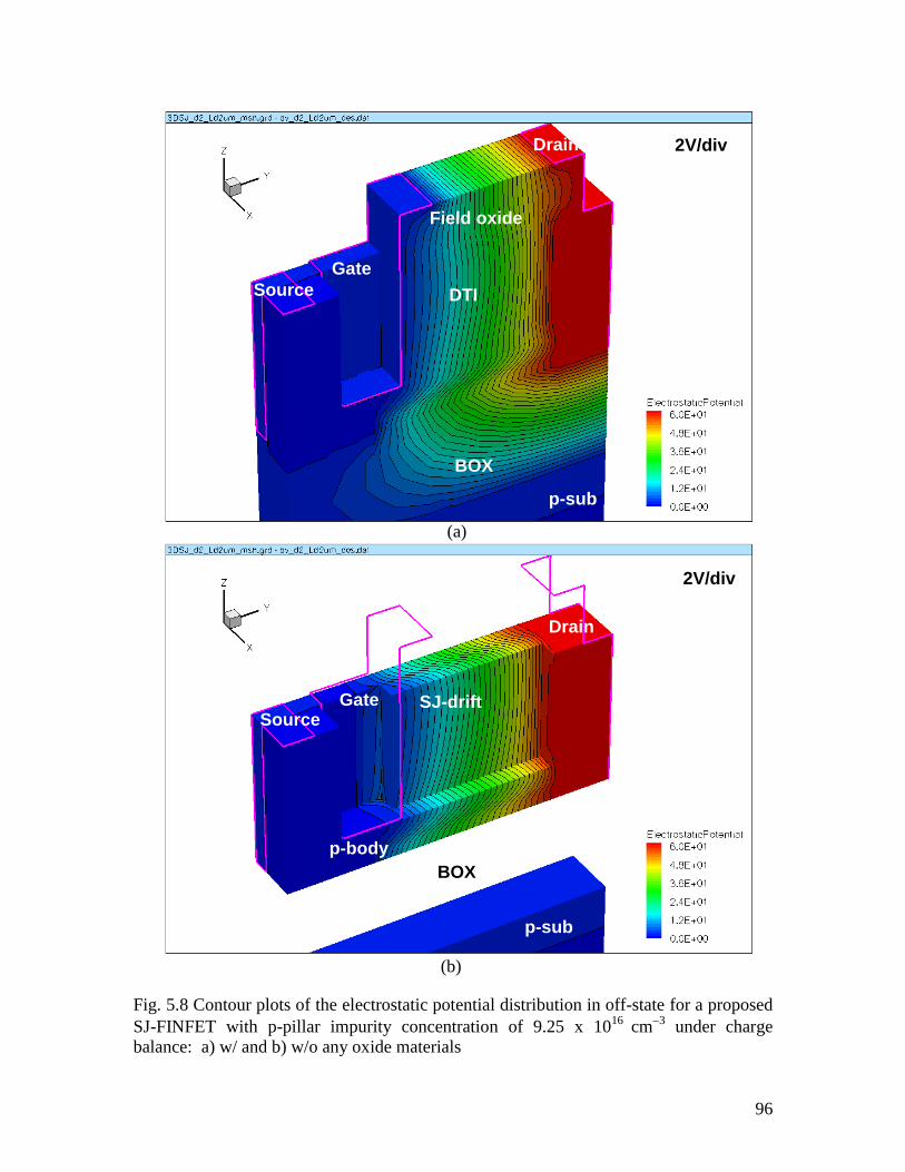
96
Fig. 5.8 Contour plots of the electrostatic potential distribution in off-state for a proposed
SJ-FINFET with p-pillar impurity concentration of 9.25 x 10¹⁶
cm3
under charge
balance: a) w/ and b) w/o any oxide materials
BOX
Field oxide
Drain
Source DTI
Gate
p-sub
Source Gate
p-body
BOX
p-sub
SJ-drift
Drain
2V/div
2V/div
(a)
(b)
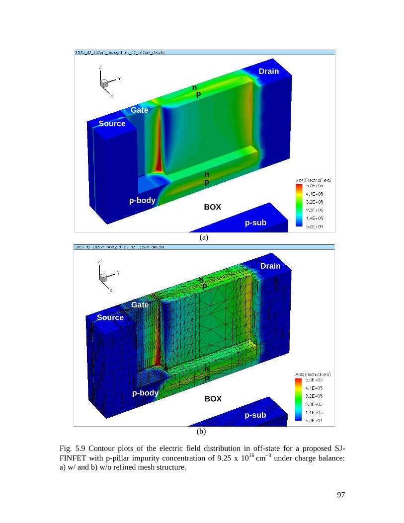
97
Fig. 5.9 Contour plots of the electric field distribution in off-state for a proposed SJ-
FINFET with p-pillar impurity concentration of 9.25 x 10¹⁶
cm3
under charge balance:
a) w/ and b) w/o refined mesh structure.
BOX
n
Drain
Source
Gate
p-sub
Source
Gate
p-body BOX
p-sub
Drain
(a)
(b)
p
BOX
n p
p-body
n p
n p
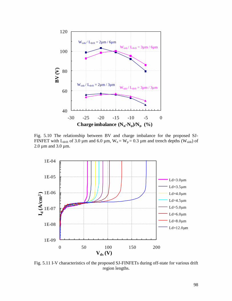
98
Fig. 5.10 The relationship between BV and charge imbalance for the proposed SJ-
FINFET with Ldrift of 3.0 µm and 6.0 µm, Wn = Wp = 0.3 µm and trench depths (Wside) of
2.0 µm and 3.0 µm.
Fig. 5.11 I-V characteristics of the proposed SJ-FINFETs during off-state for various drift
region lengths.
40
60
80
100
120
-30 -25 -20 -15 -10 -5 0
BV
(V
)
Charge imbalance (Nn-Np)/Np (%)
Wside / Ldrift = 2µm / 6µm
Wside / Ldrift = 3µm / 6µm
Wside / Ldrift = 3µm / 3µm Wside / Ldrift = 2µm / 3µm
1E-09
1E-08
1E-07
1E-06
1E-05
1E-04
0 50 100 150 200
I d(A
/cm
2 )
Vds (V)
Ld=3.0μm
Ld=3.5μm
Ld=4.0μm
Ld=4.5μm
Ld=5.0μm
Ld=6.0μm
Ld=8.0μm
Ld=12.0μm
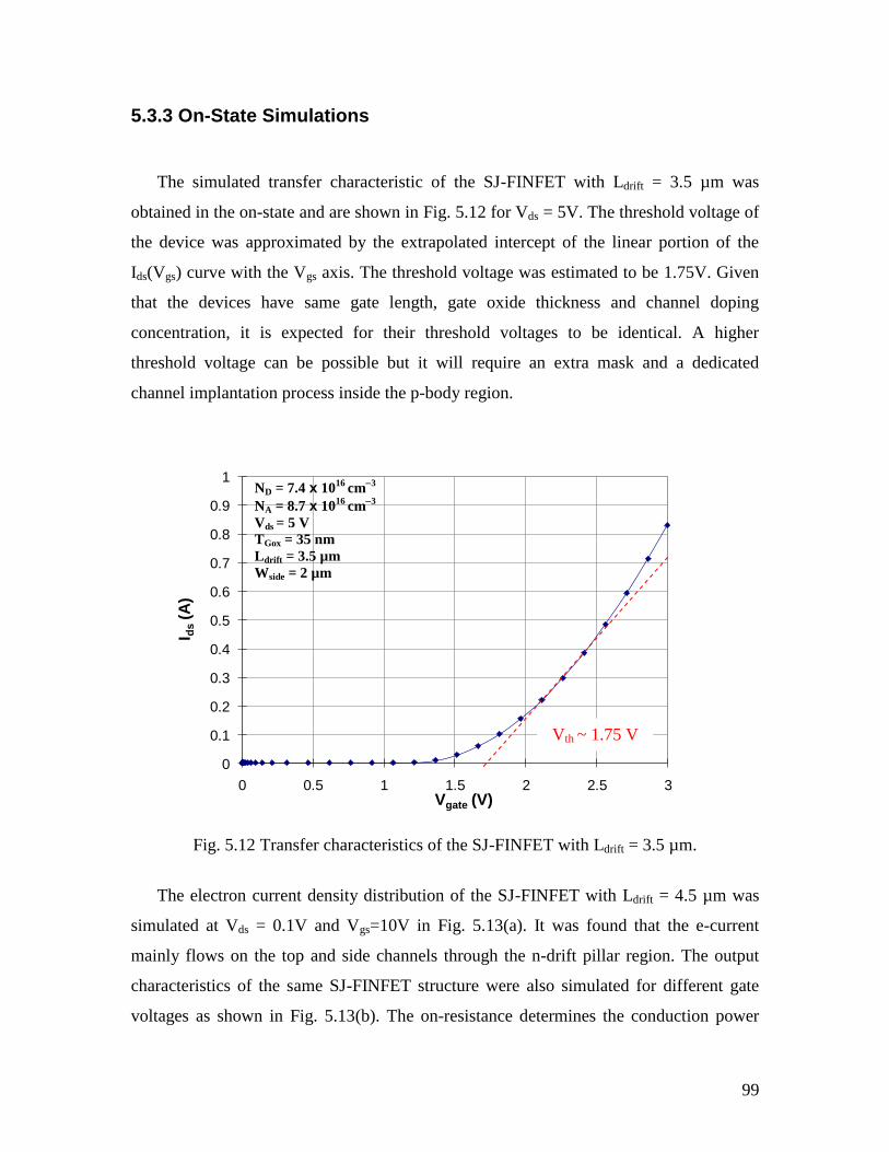
99
5.3.3 On-State Simulations
The simulated transfer characteristic of the SJ-FINFET with Ldrift = 3.5 µm was
obtained in the on-state and are shown in Fig. 5.12 for Vds = 5V. The threshold voltage of
the device was approximated by the extrapolated intercept of the linear portion of the
Ids(Vgs) curve with the Vgs axis. The threshold voltage was estimated to be 1.75V. Given
that the devices have same gate length, gate oxide thickness and channel doping
concentration, it is expected for their threshold voltages to be identical. A higher
threshold voltage can be possible but it will require an extra mask and a dedicated
channel implantation process inside the p-body region.
Fig. 5.12 Transfer characteristics of the SJ-FINFET with Ldrift = 3.5 µm.
The electron current density distribution of the SJ-FINFET with Ldrift = 4.5 µm was
simulated at Vds = 0.1V and Vgs=10V in Fig. 5.13(a). It was found that the e-current
mainly flows on the top and side channels through the n-drift pillar region. The output
characteristics of the same SJ-FINFET structure were also simulated for different gate
voltages as shown in Fig. 5.13(b). The on-resistance determines the conduction power
0
0.1
0.2
0.3
0.4
0.5
0.6
0.7
0.8
0.9
1
0 0.5 1 1.5 2 2.5 3
I ds
(A)
Vgate (V)
ND = 7.4 x 10¹⁶
cm3
NA = 8.7 x 10¹⁶
cm3
Vds = 5 V
TGox = 35 nm
Ldrift = 3.5 µm
Wside = 2 µm
Vth ~ 1.75 V

100
dissipation. In a linear region, the device acts as a resistor with almost a constant on-
resistance, Ron defined by Vds / Ids. To extract the specific on-resistance (Ron,sp), the area
factor which implies how many unit-cells can be substituted into the final device, should
be defined in the device input file. The simulated Ron,sp of the device was 0.498 mΩ∙cm2
at VG = 10V. Since the BV is independent of the SJ depth, the greater pillar height is
preferred for a higher electron current density, however the shadowing effect from the
tilted ion implantation (as addressed in the section 5.2) should be minimized along with
other process limitations such as etching selectivity, trench profile (i.e. aspect ratio),
minimum processing rule, high dislocation density in the n-epi, etc.
In Fig. 5.14, the I-V characteristics of the SJ-FINFETs with Wside = 2 µm were
simulated in the on-state for different Ldrift while the optimum charge balanced conditions
(ND= 7.4 x 10¹⁶
cm3
and NA = 9.25 x 10¹⁶
cm3
) were maintained in all cases. In this
analysis, Ldrift was varied from 3 µm to 12 µm and all other parameters were kept the
same. Note that the specific on-resistance for each Ldrift can be calculated from the plot.
As the drift length of the SJ-FINFET increases, the drain-to-source current is found to be
decreased. Since the drift resistance is proportional to the drift length, it is obvious that a
smaller amount of current flows through a longer current path.
Lastly, Fig. 5.15 plots BV and Ron,sp as a function of Ldrift for two different trench gate
depths (i.e. Wside = 2 µm or 3µm). This confirms that a low Ron,sp can be achieved by
using high aspect ratio trench. This fact can be utilized to overcome the problem of BV
sensitivity to the charge imbalance. A recommended solution is that first one should
determine a required increase of the drift region length to offset the degradation in BV
and finally to negate the resulting increase in Ron,sp by adopting a higher aspect ratio
pillars.

101
Fig. 5.13 On-state simulations: (a) electron current density distribution and (b) output
characteristics of the SJ-FINFET with Ldrift =4.5 µm and device area = 1 mm2.
0
0.2
0.4
0.6
0.8
1
1.2
1.4
1.6
1.8
2
2.2
0 0.02 0.04 0.06 0.08 0.1
I ds
(A)
Vds (V)
VG = 10 V
VG = 5 V
VG = 3 V
(a)
(b)
VG = 10 V, VDS = 0.1 V
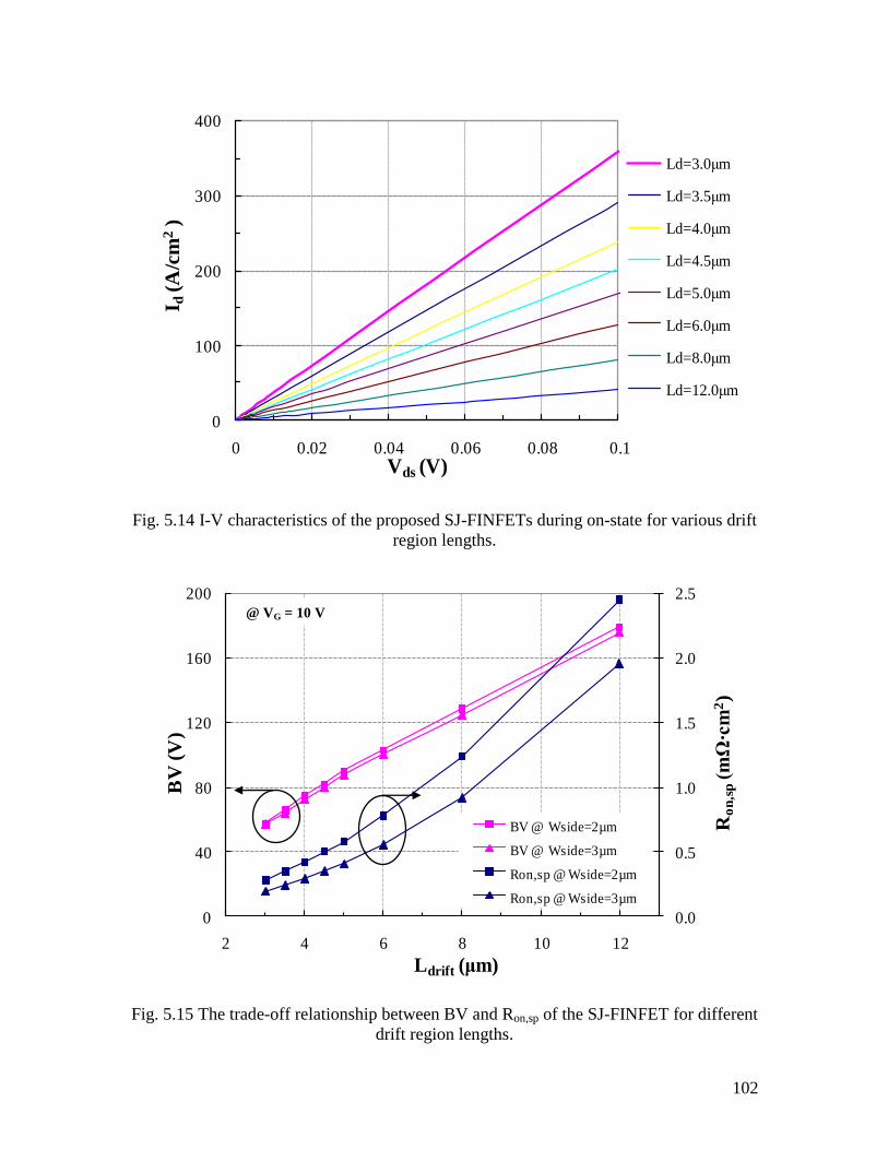
102
Fig. 5.14 I-V characteristics of the proposed SJ-FINFETs during on-state for various drift
region lengths.
Fig. 5.15 The trade-off relationship between BV and Ron,sp of the SJ-FINFET for different
drift region lengths.
0.0
0.5
1.0
1.5
2.0
2.5
0
40
80
120
160
200
2 4 6 8 10 12
Ro
n,s
p(m
Ω·cm
2)
BV
(V
)
Ldrift (μm)
BV @ Wside=2µm
BV @ Wside=3µm
Ron,sp @ Wside=2µm
Ron,sp @ Wside=3µm
@ VG = 10 V
0
100
200
300
400
0 0.02 0.04 0.06 0.08 0.1
I d(A
/cm
2 )
Vds (V)
Ld=3.0μm
Ld=3.5μm
Ld=4.0μm
Ld=4.5μm
Ld=5.0μm
Ld=6.0μm
Ld=8.0μm
Ld=12.0μm

103
5.4 Comparison with Conventional SJ-LDMOS and Si Limit
Traditional SJ devices have not yet been widely applied in low voltage (e.g. < 200V)
applications. One drawback associated with the low voltage SJ devices is that the on-
resistance is not strongly depending on the drift doping concentration because the channel
resistance starts to become comparable to the drift resistance. To resolve the issue, the SJ-
FINFET was previously proposed and simulated to obtain its electrical characteristics. In
this section, the simulated results of the SJ-FINFET device are compared with
conventional SJ-LDMOS and the ideal silicon limit. Throughout the detailed comparison
analysis, e.g. the electric field distribution, mobility and specific on-resistance profiles,
the advantages of the SJ-FINFET structure have been verified and confirmed prior to the
actual device fabrication. A conventional planar gate SJ-LDMOS structure was designed
to be identical as the SJ-FINFET structure, except the 3D trench gate and its U-shaped
n/p pillars. The simulated performance of the SJ-FINFET structure was also compared
with the previously published data.
5.4.1 Specific On-Resistance and Mobility Profiles
Fig. 5.16 presents the specific on-resistance profiles along the SJ-FINFET cross
section with Ldrift = 3 µm. In comparison with the conventional SJ-LDMOS structure, the
proposed SJ-FINFET devices with the trench depths of 2 µm and 3 µm demonstrate a
58% and 74% reduction in channel resistance, and a 44% and 60% reduction in drift-
resistance, respectively. This is due to the fact that the majority of electron current is
concentrated near the top surface of n-drift layer in the conventional planar gate SJ device.
However, the proposed SJ device uses an embedded trench gate not only to reduce the
channel resistance but also to relax the electron current crowding near the top of the n-
drift region pillar. It also suggests that increasing the trench depth is not effective in
reducing the drift resistance of the conventional SJ-LDMOS transistor with short drift
region length. To achieve more uniformly distributed electron current flow in the n-drift
region of the SJ-FINFET structure, the formations of deep trench source/drain junctions
are necessary.
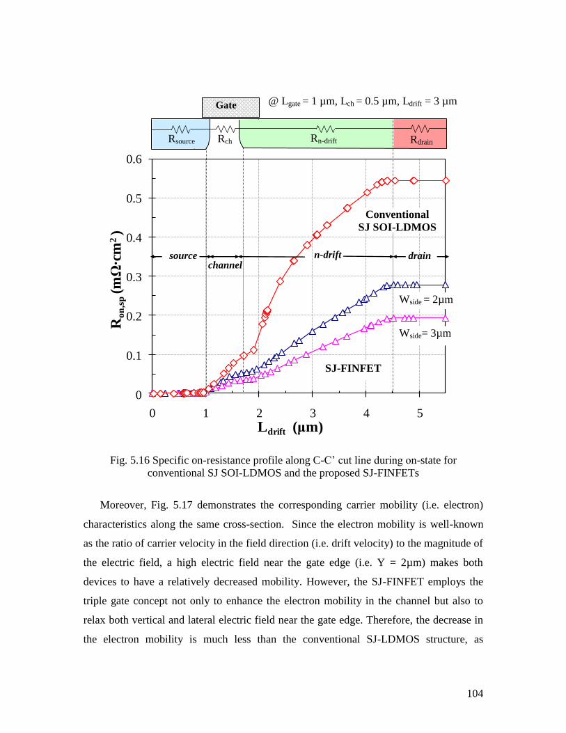
104
Fig. 5.16 Specific on-resistance profile along C-C‟ cut line during on-state for
conventional SJ SOI-LDMOS and the proposed SJ-FINFETs
Moreover, Fig. 5.17 demonstrates the corresponding carrier mobility (i.e. electron)
characteristics along the same cross-section. Since the electron mobility is well-known
as the ratio of carrier velocity in the field direction (i.e. drift velocity) to the magnitude of
the electric field, a high electric field near the gate edge (i.e. Y = 2µm) makes both
devices to have a relatively decreased mobility. However, the SJ-FINFET employs the
triple gate concept not only to enhance the electron mobility in the channel but also to
relax both vertical and lateral electric field near the gate edge. Therefore, the decrease in
the electron mobility is much less than the conventional SJ-LDMOS structure, as
0
0.1
0.2
0.3
0.4
0.5
0.6
0 1 2 3 4 5
Ron
,sp
(mΩ·c
m2 )
Ldrift (μm)
@ Lgate = 1 µm, Lch = 0.5 µm, Ldrift = 3 µm
n-drift source
Wside= 3µm
Wside = 2µm
SJ-FINFET
drain channel
Rch Rn-drift Rdrain Rsource
Gate
Conventional
SJ SOI-LDMOS
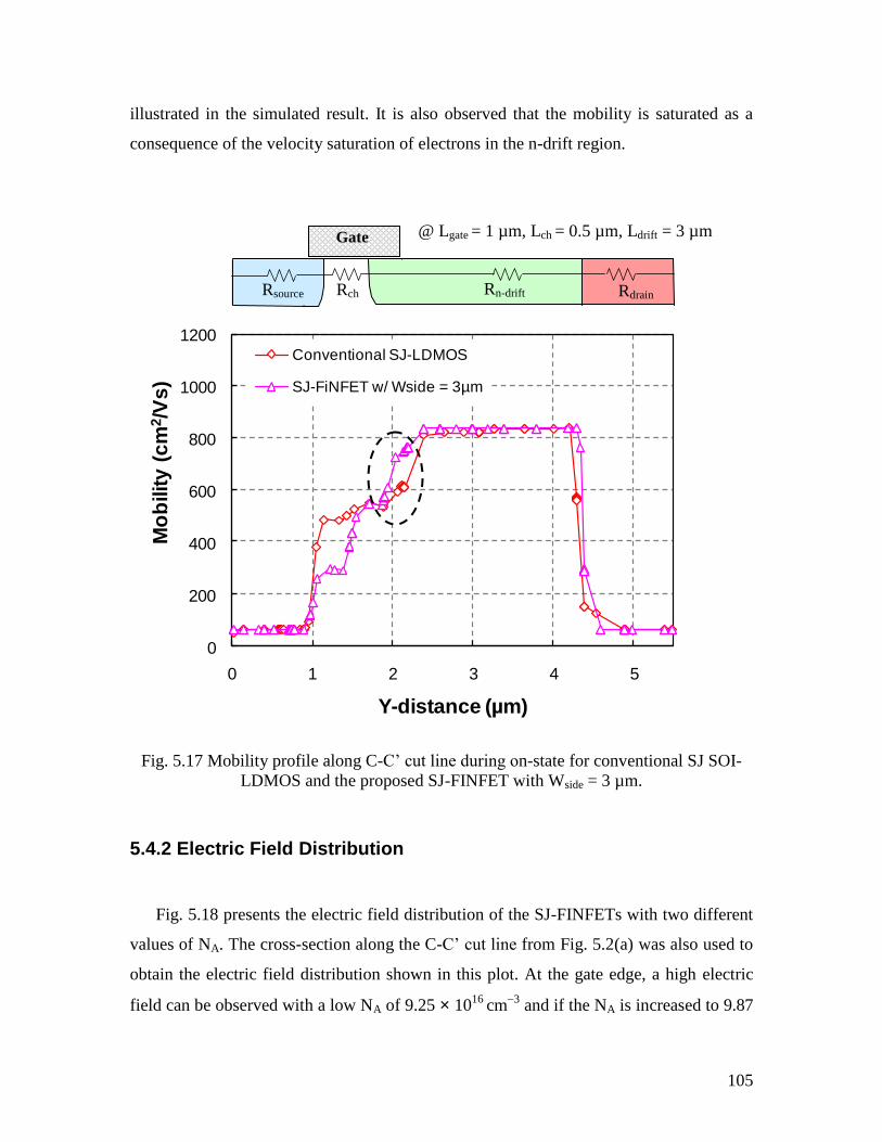
105
illustrated in the simulated result. It is also observed that the mobility is saturated as a
consequence of the velocity saturation of electrons in the n-drift region.
Fig. 5.17 Mobility profile along C-C‟ cut line during on-state for conventional SJ SOI-
LDMOS and the proposed SJ-FINFET with Wside = 3 µm.
5.4.2 Electric Field Distribution
Fig. 5.18 presents the electric field distribution of the SJ-FINFETs with two different
values of NA. The cross-section along the C-C‟ cut line from Fig. 5.2(a) was also used to
obtain the electric field distribution shown in this plot. At the gate edge, a high electric
field can be observed with a low NA of 9.25 × 10¹⁶
cm3
and if the NA is increased to 9.87
0
200
400
600
800
1000
1200
0 1 2 3 4 5
Mo
bilit
y (
cm
2/V
s)
Y-distance (µm)
Conventional SJ-LDMOS
SJ-FiNFET w/ Wside = 3µm
@ Lgate = 1 µm, Lch = 0.5 µm, Ldrift = 3 µm
Rch Rn-drift Rdrain Rsource
Gate
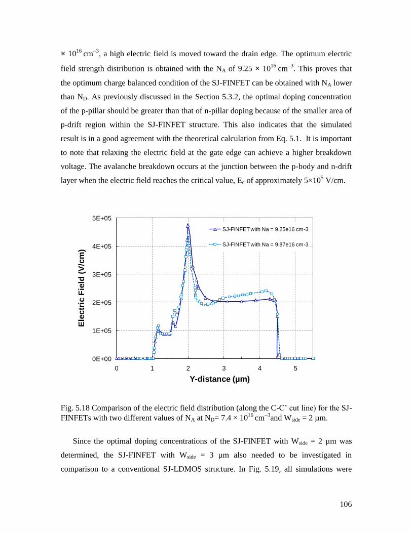
106
× 1016
cm3
, a high electric field is moved toward the drain edge. The optimum electric
field strength distribution is obtained with the NA of 9.25 × 10¹⁶
cm3
. This proves that
the optimum charge balanced condition of the SJ-FINFET can be obtained with NA lower
than ND. As previously discussed in the Section 5.3.2, the optimal doping concentration
of the p-pillar should be greater than that of n-pillar doping because of the smaller area of
p-drift region within the SJ-FINFET structure. This also indicates that the simulated
result is in a good agreement with the theoretical calculation from Eq. 5.1. It is important
to note that relaxing the electric field at the gate edge can achieve a higher breakdown
voltage. The avalanche breakdown occurs at the junction between the p-body and n-drift
layer when the electric field reaches the critical value, Ec of approximately 5×10⁵ V/cm.
Fig. 5.18 Comparison of the electric field distribution (along the C-C‟ cut line) for the SJ-
FINFETs with two different values of NA at ND= 7.4 × 10¹⁶
cm3
and Wside = 2 µm.
Since the optimal doping concentrations of the SJ-FINFET with Wside = 2 µm was
determined, the SJ-FINFET with Wside = 3 µm also needed to be investigated in
comparison to a conventional SJ-LDMOS structure. In Fig. 5.19, all simulations were
0E+00
1E+05
2E+05
3E+05
4E+05
5E+05
0 1 2 3 4 5
Ele
ctr
ic F
ield
(V
/cm
)
Y-distance (µm)
SJ-FINFET with Na = 9.25e16 cm-3
SJ-FINFET with Na = 9.87e16 cm-3
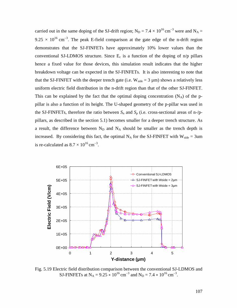
107
carried out in the same doping of the SJ-drift region; ND = 7.4 × 10¹⁶
cm3
were and NA =
9.25 × 10¹⁶
cm3
. The peak E-field comparison at the gate edge of the n-drift region
demonstrates that the SJ-FINFETs have approximately 10% lower values than the
conventional SJ-LDMOS structure. Since Ec is a function of the doping of n/p pillars
hence a fixed value for those devices, this simulation result indicates that the higher
breakdown voltage can be expected in the SJ-FINFETs. It is also interesting to note that
that the SJ-FINFET with the deeper trench gate (i.e. Wside = 3 µm) shows a relatively less
uniform electric field distribution in the n-drift region than that of the other SJ-FINFET.
This can be explained by the fact that the optimal doping concentration (NA) of the p-
pillar is also a function of its height. The U-shaped geometry of the p-pillar was used in
the SJ-FINFETs, therefore the ratio between Sn and Sp (i.e. cross-sectional areas of n-/p-
pillars, as described in the section 5.1) becomes smaller for a deeper trench structure. As
a result, the difference between ND and NA should be smaller as the trench depth is
increased. By considering this fact, the optimal NA for the SJ-FINFET with Wside = 3um
is re-calculated as 8.7 × 10¹⁶
cm3
.
Fig. 5.19 Electric field distribution comparison between the conventional SJ-LDMOS and
SJ-FINFETs at NA = 9.25 × 10¹⁶
cm3
and ND = 7.4 × 10¹⁶
cm3
.
0E+00
1E+05
2E+05
3E+05
4E+05
5E+05
6E+05
0 1 2 3 4 5
Ele
ctr
ic F
ield
(V
/cm
)
Y-distance (µm)
Conventional SJ-LDMOS
SJ-FINFET with Wside = 2µm
SJ-FINFET with Wside = 3µm
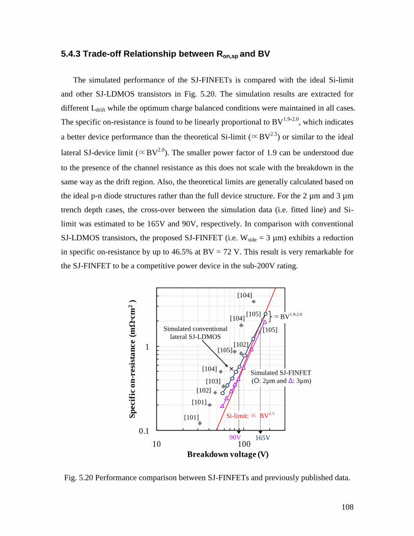
108
5.4.3 Trade-off Relationship between Ron,sp and BV
The simulated performance of the SJ-FINFETs is compared with the ideal Si-limit
and other SJ-LDMOS transistors in Fig. 5.20. The simulation results are extracted for
different Ldrift while the optimum charge balanced conditions were maintained in all cases.
The specific on-resistance is found to be linearly proportional to BV1.9-2.0
, which indicates
a better device performance than the theoretical Si-limit (∝BV2.5
) or similar to the ideal
lateral SJ-device limit (∝BV2.0
). The smaller power factor of 1.9 can be understood due
to the presence of the channel resistance as this does not scale with the breakdown in the
same way as the drift region. Also, the theoretical limits are generally calculated based on
the ideal p-n diode structures rather than the full device structure. For the 2 µm and 3 µm
trench depth cases, the cross-over between the simulation data (i.e. fitted line) and Si-
limit was estimated to be 165V and 90V, respectively. In comparison with conventional
SJ-LDMOS transistors, the proposed SJ-FINFET (i.e. Wside = 3 µm) exhibits a reduction
in specific on-resistance by up to 46.5% at BV = 72 V. This result is very remarkable for
the SJ-FINFET to be a competitive power device in the sub-200V rating.
Fig. 5.20 Performance comparison between SJ-FINFETs and previously published data.
0.1
1
10 100
Sp
ecif
ic o
n-r
esi
sta
nce (
mΩ·c
m2
)
Breakdown voltage (V)
∝BV1.9-2.0
[102]
[103]
[104]
[105]
Simulated conventional
lateral SJ-LDMOS
Simulated SJ-FINFET
(О: 2µm and Δ: 3µm)
Si-limit: ∝ BV2.5
90V
165V
[102]
[101]
[105]
[104]
[105]
[104]
[101]

109
5.5 Summary
In this chapter, a novel device structure suitable for practical implementation of
lateral superjunction FINFET (SJ-FINFET) on SOI platform was proposed and studied
for next generation of sub-200V rating power applications. The SJ-FINFET structure
with heavily doped alternating U-shaped n/p pillars was developed to minimize both
channel and drift resistances, and to mitigate electron current crowding near the top of n-
drift region. The feasibility of the design concept was validated by a two dimensional
process simulator, TSUPREM-4TM
for three important process modules such as a) P-body
formation, b) SJ-drift formation, and c) N+ source/drain contact formation. In comparison
with the conventional planar gate SJ-LDMOS device, the SJ-FINFET device was also
investigated for different trench gate depths and drift lengths. Three dimensional
numerical simulations with ISE-DESSISTM
have been performed to analyze the influence
of device parameters on the charge imbalance and the trade-off relationship between BV
and Ron,sp. To summarize, the SJ-FINFET structure exhibits low Ron,sp with voltage
ratings below 200V. With the optimized charge balanced SJ-drift region, the SJ-FINFETs
were found to be able to overcome the Si-limit with the breakdown voltages of 165 V and
90 V, respectively. This is a positive indication that the SJ-FINFET can become a
competitive power device for sub-200V applications [106]. In the next chapter, the
detailed fabrication process of the SJ-FINFET would be presented followed by the
experimental measurement results of both SJ-FINFET and SJ-LDMOS devices. The
issues related to the optimization of the SJ structure and process integration would be also
discussed.
110
Chapter 6 Device Fabrication and Characterization of
the SJ-FINFET on SOI
The focus of this chapter is to explore the suitability of the SJ-FINFET in low voltage
applications. It presents a CMOS-compatible lateral SJ-FINFET on a SOI substrate.
Using tilted ion implantation and deep trench RIE techniques, a SJ-FINFET consists of a
corrugated 3D trench gate and SJ drift region was implemented in a submicron CMOS
technology. The performance advantage of the SJ-FINFET over the conventional SJ-
LDMOSFET was also verified experimentally. The current work represents the first
experimental confirmation that the super-junction concept is advantageous for sub-100V
applications. In the following sub-sections, the detailed fabrication process scheme is
presented followed by various electrical measurement results of the devices. The issues
related to the optimization of the SJ-structure and process integration are also discussed.
6.1 Process Design Considerations
The first-generation lateral SJ-FINFET was developed at the Nanoelectronic
Fabrication Facility (NFF) in Hong Kong University of Science and Technology
(HKUST) to validate its performance advantages over the conventional planar gate SJ-
LDMOS structure. The prototype devices were fabricated on a customized 4” SOI
(Silicon-On-Insulator) substrate from a wafer supplier, Ultrasil Corporation. As described
in the previous chapter, the charge balance between the alternating n-/p- pillars is
strongly affected by the substrate-assisted depletion (SAD) effect. To eliminate this
dependence, a high quality silicon fusion bonded (SFB) SOI wafer with a thick buried
oxide layer was selected as a starting material. The substrate consists of an n-type
epitaxial device layer with a <100> surface crystallographic orientation and a resistivity
of 0.1 to 0.2 Ω∙cm. The resistivity was chosen to allow the doping concentration of the n-
drift region to be as close as its optimal value (i.e. ND = 7.4 x 10¹⁶
cm3
), as calculated
from the section 5.1. The thickness of the device layer, handle layer and buried oxide

111
layer were 3.5µm, 500µm, and 2µm, respectively. The detailed specifications of the SOI
wafer are described in Table 6.1.
Table 6.1 Parameters and specifications of the SOI wafer used in the fabrication
Parameters Specifications
SOI Wafer: Silicon Fusion Bonding (SFB)
Diameter 100 ± 0.2 mm
Crystal Orientation (100) ± 0.5 degree
Flat Standard: <100>
Overall Thickness 505.5 ± 25 µm
Thickness Variation < 2 µm
Surface/Backside Polished / Lapped
Device Layer (Epi.)
Type / Dopant N-type / Phosphorus
Thickness 3.5 ± 0.5 µm
Resistivity 0.1 – 0.2 Ω∙cm
Buried Oxide Layer (BOX)
Type of Oxide Thermal Oxide
Thickness 2.0 ± 0.1 µm
Handle Wafer (Substrate)
Type / Dopant P-type / Boron
Thickness 500 ± 25 µm
Resistivity 60 – 70 Ω∙cm
The SJ-FINFET fabrication was compatible with a standard 0.5µm CMOS flow. To
realize the SJ-FINFET, new optional process modules were developed that can be added
to the baseline CMOS technology. Fig. 6.1 represents a condensed flow chart for the SJ-
FINFET process. For example, two different deep trench etches are necessary prior to the
formation of the gate electrode. The sidewall doping of the trenches can be performed by
a tilted ion implantation. With additional thermal diffusion steps, the doped trench
regions are activated as the P-body and P-drift (i.e. SJ-drift) regions, respectively. Gate
lithography and etch, gate oxidation, in-situ (n-doped) amorphous silicon deposition,
poly-crystallization, poly-silicon etch and doping annealing are then carried out to form
the gate electrode. When a positive potential higher than the threshold voltage is applied
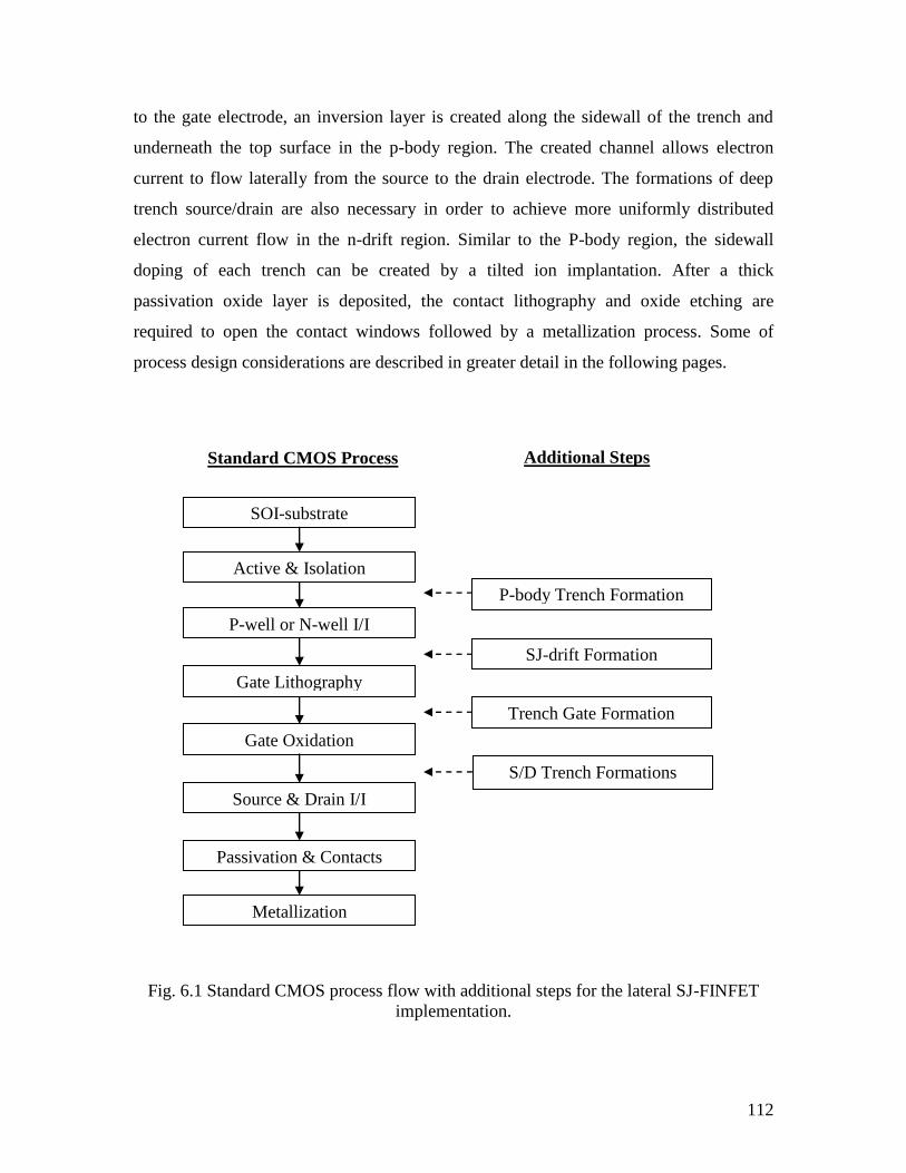
112
to the gate electrode, an inversion layer is created along the sidewall of the trench and
underneath the top surface in the p-body region. The created channel allows electron
current to flow laterally from the source to the drain electrode. The formations of deep
trench source/drain are also necessary in order to achieve more uniformly distributed
electron current flow in the n-drift region. Similar to the P-body region, the sidewall
doping of each trench can be created by a tilted ion implantation. After a thick
passivation oxide layer is deposited, the contact lithography and oxide etching are
required to open the contact windows followed by a metallization process. Some of
process design considerations are described in greater detail in the following pages.
Fig. 6.1 Standard CMOS process flow with additional steps for the lateral SJ-FINFET
implementation.
Standard CMOS Process Additional Steps
P-body Trench Formation
SJ-drift Formation
Trench Gate Formation
SOI-substrate
Active & Isolation
P-well or N-well I/I
Gate Lithography
Gate Oxidation
Source & Drain I/I
Passivation & Contacts
Metallization
S/D Trench Formations

113
Deep Trench Isolation (DTI) process
LOCOS (LOCal Oxidation of Silicon) isolation technique is the most popular scheme
in bulk CMOS technology. In this technique, active areas are protected by a silicon
nitride layer and the field oxide is thermally grown outside the active area. However, the
lateral encroachment of the field oxide, called “bird‟s beak”, occurs at the edge of active
area and is proportional to the thickness of the field oxide [107]. One solution to this
problem is to use a STI (Shallow Trench Isolation) process. This process is generally
used on CMOS process technology nodes of 250 nanometers and smaller. However, a
deep trench isolation (DTI) technique starts to become more popular in the recent years,
especially for power electronic devices. Since the SJ-FINFET structure requires its
channel region on both top surface and the sidewall of the trenches, the DTI process was
chosen as an isolation technique. By connecting the isolation region to the thick buried
oxide layer, more complete isolation could be achieved. Fig. 6.2 demonstrates the
processing steps required to create the DTI region as an example. First, a trench is etched
into the substrate. After under-etching of the oxide pad, a thermal oxide is grown inside
the trench. After the formation of a thin oxide layer, the rest of the trench is filled with an
oxide followed by the thermal densification. The excessive oxide is removed with CMP
and then the nitride mask can be finally removed as shown in this figure.
Fig. 6.2 Six sequential processing steps required for the deep trench isolation region.
(a) Stack and trench etching (b) Pad oxide under-etching (c) Liner oxidation
(f) Nitride strip (e) CMP (d) CVD oxide gap-fill
Pad Oxide
Isolat. Oxide
Isolat. Oxide
Isolat. Oxide
Silicon Silicon
Nitride Nitride
Resist Resist Liner Oxide

114
P-body and SJ-drift implantations
The P-body implantation was one of critical steps in the proposed SJ-FINFET
structure. The implantation dose must be high enough to degrade the parasitic BJT
structure while minimizing the damages to the surface silicon layer. Carrier lifetime
depends on the impurity dose and the thermal budge in later processing steps. Based on
the literature and process simulation results (refers to the section 5.2.1), a high angle B+
tilted ion implantation with an energy of 190 keV and doses between 2×10¹⁴
/cm2 and
3×10¹⁴
/cm2 were studied experimentally. This resulted in a projected range of 5100Å
with a standard deviation of approximately 900 Å. The projected range could be adjusted
by choosing different implantation energy, however 190 keV was the maximum
allowable implant energy offered from NFF at HKUST. Since the lateral diffusion length
of the P-body region (i.e. width of the p-body region) was targeted as 1.2µm, the
cumulated thermal annealing period throughout the overall fabrication process had to be
considered. Also, the high dose implantation should be carried out before the gate
oxidation to avoid damaging the thin gate oxide layer. Another critical process step was
the SJ-drift formation by a low angle tilted implantation. Since the widths of alternating
n/p pillars were limited by the processing design rule, it was difficult to create the width
of the p-pillar narrower than 0.5 µm. To overcome such a processing limit, the high
doped alternating U-shaped n/p pillars were formed by a combination of the B+ tilted ion
implantation and deep trench RIE techniques. With accurate control of the thermal
diffusion process, the width of the alternating pillars could be narrower than the
minimum processing rule. The tilted ion implantation with energy of 45 keV and four
different doses of 2×10¹³
/cm2, 4×10
13/cm
2, 6×10
13/cm
2, and 1×10
14/cm
2 were examined
experimentally. The target width of the p-pillar was 0.3 µm.
Short channel effect
As the channel length of a MOSFET is reduced, it starts to behave different from a
transistor with a long channel. The deviation arises as a result of two dimensional
potential distribution and high electric field in the channel region. In particular, a

115
threshold voltage rolls off as the channel length is reduced. The short channel effect
(SCE) complicates device operation and degrade device performance. As a result, this
effect needs to be minimized so that a short channel device can preserve the electrical
characteristics of a long channel device.
The minimum channel length, Lmin in which a long channel sub-threshold behavior
can be preserved can be calculated from the empirical relation [108].
1/32DSoxjmin ])W(WtX[0.4L (Eq.6.1)
where jX is the junction depth in µm, oxt is the thickness of gate oxide in Å, and
)W(W DS is the sum of source and drain depletion width in µm.
Thermal budget and wafer warpage
Dopant redistribution is one of the major concerns for the thermal budget in process
integration. In addition, the thermal budget induces a stress from various interfaces
between the substrate and other deposited layers. Since the SJ-FINFET fabrication
requires a deep trench isolation region filled with LTO and the silicon nitride layer as a
hard mask, the wafer warpage should be considered as another process design issue. To
minimize the degree of the wafer warpage, several methods had to be considered. First,
the low stress silicon-rich nitride was used as the hard-masking layer, instead of the
stoichiometric silicon nitride because it induces a less tensile stress. The thickness of the
deposited nitride layer was further reduced to obtain even less tensile stress. Another
method was that the thermal SiO2 liner (compressive stress) was grown inside the trench
prior to the LTO gap-filling and densification processes (tensile stress). This results that a
high tensile stress induced by LTO could be reduced. Also, all stress layers deposited at
the backside of the wafer were not completely removed for the stress neutralization
purpose. Lastly, the thermal budget was limited to 900 °C after all high dose
implantations.

116
6.2 SJ-FINFET in a 0.5µm Standard CMOS Process Flow
In this section, the process flow of the lateral SJ-FINFET will be briefly discussed
with reference to Fig. 6.3, which includes the three dimensional schematic view of each
major processing step. A total of nine masks were used in this fabrication.
MASK #1 – Active / Isolation
The fabrication started with the dry oxidation of a 300Å thin pad oxide on the SOI
wafer followed by a 2500Å thick nitride deposition. As described in the previous section
(see Fig. 6.2), Mask #1 was then used to define active and isolation regions. First, a deep
trench (depth = 3.5 µm) was etched into the n-epi device layer. After under-etching of the
oxide pad, a 300 Å thin dry oxide liner was grown inside the trench. After the formation
of the liner, the rest of the trench was filled with a 4.5 µm thick of low temperature oxide
(LTO) at 425°C by a CVD furnace. This was then followed by the thermal densification
at 900°C for 30 minutes in N2 gas. Unlike PECVD or thermal SiO2 films, which have
compressive stress, LTO films are normally deposited with tensile stress, ranging from 1
x 108 to 3 x 10
9 dynes/cm
2 [109]. Moreover, they exhibit lower film densities and high
etch rates in buffered hydrofluoric acid (BHF). Therefore, the densification process was
necessary to obtain a higher film density and low HF etch rate. Not only this helps to get
more stable oxide but also it removes H contamination which is incorporated into the film
both during deposition, including PECVD, and post deposition through moisture
absorption. For the planarization purpose, the excessive oxide was removed with CMP
and then the nitride layer was completely wet-etched at 165°C by H3PO4. Consequently,
this leads to define both active and isolation regions on the SOI wafer. Since our research
is mainly focused on the SJ-FINFET device fabrication, the active region will be only
considered in the next processing steps.
MASK #2 – P-body
As illustrated in Fig. 6.3(a) to (e), another pad oxide of 300Å was thermally grown on
the top of the SOI substrate and then Mask #2 was used to define the specific location
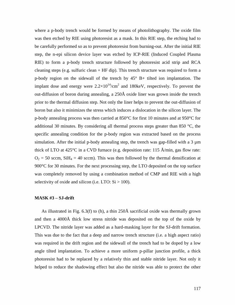
117
where a p-body trench would be formed by means of photolithography. The oxide film
was then etched by RIE using photoresist as a mask. In this RIE step, the etching had to
be carefully performed so as to prevent photoresist from burning-out. After the initial RIE
step, the n-epi silicon device layer was etched by ICP-RIE (Induced Coupled Plasma
RIE) to form a p-body trench structure followed by photoresist acid strip and RCA
cleaning steps (e.g. sulfuric clean + HF dip). This trench structure was required to form a
p-body region on the sidewall of the trench by 45° B+ tilted ion implantation. The
implant dose and energy were 2.2×10¹⁴
/cm2 and 180keV, respectively. To prevent the
out-diffusion of boron during annealing, a 250Å oxide liner was grown inside the trench
prior to the thermal diffusion step. Not only the liner helps to prevent the out-diffusion of
boron but also it minimizes the stress which induces a dislocation in the silicon layer. The
p-body annealing process was then carried at 850°C for first 10 minutes and at 950°C for
additional 30 minutes. By considering all thermal process steps greater than 850 °C, the
specific annealing condition for the p-body region was extracted based on the process
simulation. After the initial p-body annealing step, the trench was gap-filled with a 3 µm
thick of LTO at 425°C in a CVD furnace (e.g. deposition rate: 115 Å/min, gas flow rate:
O2 = 50 sccm, SiH4 = 40 sccm). This was then followed by the thermal densification at
900°C for 30 minutes. For the next processing step, the LTO deposited on the top surface
was completely removed by using a combination method of CMP and RIE with a high
selectivity of oxide and silicon (i.e. LTO: Si > 100).
MASK #3 – SJ-drift
As illustrated in Fig. 6.3(f) to (h), a thin 250Å sacrificial oxide was thermally grown
and then a 4000Å thick low stress nitride was deposited on the top of the oxide by
LPCVD. The nitride layer was added as a hard-masking layer for the SJ-drift formation.
This was due to the fact that a deep and narrow trench structure (i.e. a high aspect ratio)
was required in the drift region and the sidewall of the trench had to be doped by a low
angle tilted implantation. To achieve a more uniform p-pillar junction profile, a thick
photoresist had to be replaced by a relatively thin and stable nitride layer. Not only it
helped to reduce the shadowing effect but also the nitride was able to protect the other

118
silicon active area from the high energy implantation. After Mask #3 was used to define
the drift trench pattern, the nitride layer was etched and stopped by an end-point detection
method. This was then followed by ICP-RIE to create the drift trench structure with a
depth of 2.6 µm and a width of 0.6 µm. After the trench formation, the sidewall doping of
the trench was carried out by a 12° B+ tilted implantation with energy of 45 keV and four
different doses of 2×10¹³
/cm2, 4×10
13/cm
2, 6×10
13/cm
2, and 1×10
14/cm
2 for each different
SOI wafer. To obtain the optimal charge balanced condition in the SJ-drift region, it was
necessary for each SOI wafer to have a different charge imbalance (%) condition. Since
the p-drift region should be connected to the p-body and eventually to p+ body contact to
form a SJ-diode structure, a 45° B+ tilted implantation with energy of 80 keV and dose of
3.5×10¹³
/cm2 was also carried out with 90° and 270° rotations of the SOI wafer, as shown
in Fig. 6.3(g). Similar to the earlier p-body trench structure, the drift trench was also
filled with LTO followed by densification and CMP planarization steps. After that, the
nitride hard mask was completely removed by H3PO4.
MASK #4 – Trench Gate
As illustrated in Fig. 6.3(i) to (j), a thin 250Å pad oxide was first grown and a high
resolution photoresist was spin-coated and soft-baked on the top of the oxide. After the
photoresist was patterned with Mask #4, another high aspect ratio trench was formed by
ICP-RIE. This was then followed by the pad oxide removal and gate oxidation steps. A
high quality 35nm thin oxide was grown as a gate oxide at 950°C in dry O2. The quality
of the gate oxide is very crucial in determining the performance of the device. To
enhance the quality of the oxide, a small amount of NH3 was introduced into the thermal
growth cycle to reduce the amount of the mobile ionic charge in the oxide. After the gate
oxide growth, the substrate was immediately deposited by in-situ n-doped amorphous
silicon at 570°C. In a conventional CMOS process, a polysilicon gate is doped
simultaneously with a source/drain implant step. However, the SJ-FINFET requires a
corrugated 3D trench MOS gate and this makes the polysilicon gate difficult to be doped
by an implantation technique. Hence, a polysilicon deposition step had to be replaced by
an n-doped amorphous silicon deposition and then re-crystallized into the n-doped

119
polysilicon gate by RTP (1000 °C and 30 seconds). To avoid the wafer warpage issue, the
poly-silicon deposited at the backside of the SOI wafer was completely removed prior to
the RTP step.
MASK #5 –Gate Poly
As illustrated in Fig. 6.3(k), the conventional gate mask (i.e. Mask #5) was used to
define the entire gate electrode. For a better step coverage, the polysilicon was etched by
ICP-RIE and stopped at the oxide interface by end-point-detection. For comparison
purpose, the planar gate SJ-LDMOS devices were also fabricated on the same wafer
without the previous trench gate mask (i.e. Mask #4).
MASK #6 – N+ source / drain
As shown in Fig. 6.3(l) to (o), the formations of deep trench source/drain were
necessary to achieve more uniformly distributed electron current flow in the n-drift
region. Mask #2 was re-used to ensure that a high energy n+ source implantation do not
block the p-body tail underneath the n+ source region. Mask #6 was then used to define
the n+ drain region. The sidewall doping of each trench was carried out by a 45° titled
dual-implant of n-type dopant species such as arsenic and phosphorus. Since the two
implants were identically masked, the greater diffusivity of the phosphorus meant that it
would diffuse laterally in advance of the arsenic during annealing of the implant.
Therefore, the arsenic provides a low contact resistance while the phosphorus provides a
more gentle junction curvature.
MASK #7 – P+ contact
As demonstrated in Fig. 6.3(p) to (r), the photoresist was patterned using the Mask #7.
This was followed by dry etching process using plasma, thereby forming a 3µm depth of
trench structure as shown in Fig. 6.3(q). This trench structure was required for p+ contact
implant. Boron implantation with energy of 180keV and dose of 5×10¹⁴
/cm2 was
implemented and then a 4µm thick LTO passivation layer was deposited, densified, and

120
planarized. The passivation oxide should be thick enough to reduce the parasitic
capacitance between the metal pad and the substrate.
MASK #8 – Contact openings
Mask #8 was used to open the contact windows for the gate and source/drain contacts,
as shown in Fig. 6.3(s). To open the contact windows, a 3µm thick LTO filled in the
trenches was initially removed by RIE and then the oxide residues were completely
removed by a chemical etching to ensure a good electrical contact between the metal
wiring layer and the silicon.
MASK #9 – Metallization
A 1 µm of aluminum (Al-1wt% Si) layer was sputtered on the SOI wafer, at a
sputtering rate of 182 Å/sec. Mask #8 was used for metal patterning as illustrated in Fig.
6.3(t). Aluminum was dry etched at an etching rate of 1500 Å/min and the photoresist
was then removed by an O2 plasma ashing. In the final step, the wafer was annealed in a
forming gas (5% hydrogen, 95% nitrogen) for 30 minutes at 400 °C to reduce the contact
resistance and the interface trapped charge in the gate oxide.
Process Specifications
More detailed information such as the process step number, processing condition, and
equipment are summarized in Appendix-V. The process was characterized at various
stages. The typical process and electrical parameters obtained from the fabrication test
structure are listed in Table 6.2. The layer thickness and step height were measured using
the NanoSpec 4000 and the Alpha-Step 200 surface profiler. The sheet resistance of the
poly gate was measured using a 4-pint probe. The contact resistance was obtained from
the measurement of the 6-terminal Kelvin structure [110].
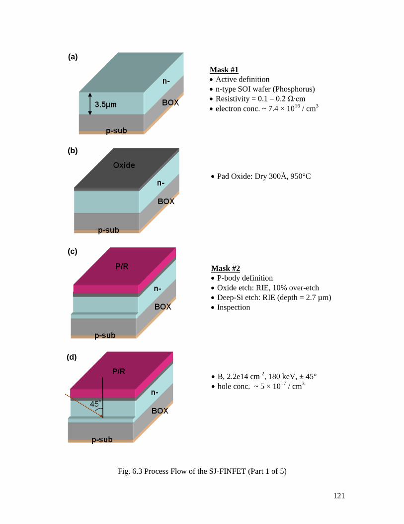
121
Fig. 6.3 Process Flow of the SJ-FINFET (Part 1 of 5)
(a)
(b)
(c)
(d)
Mask #1
Active definition
n-type SOI wafer (Phosphorus)
Resistivity = 0.1 – 0.2 Ω∙cm
electron conc. ~ 7.4 × 10¹⁶
/ cm3
Pad Oxide: Dry 300Å, 950°C
Mask #2
P-body definition
Oxide etch: RIE, 10% over-etch
Deep-Si etch: RIE (depth = 2.7 µm)
Inspection
B, 2.2e14 cm-2
, 180 keV, ± 45°
hole conc. ~ 5 × 10¹⁷
/ cm3
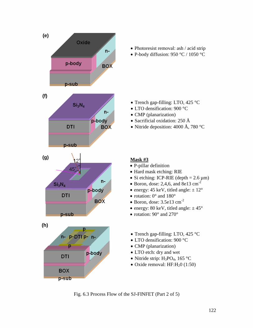
122
Fig. 6.3 Process Flow of the SJ-FINFET (Part 2 of 5)
(e)
(f)
(g)
(h)
Photoresist removal: ash / acid strip
P-body diffusion: 950 °C / 1050 °C
Trench gap-filling: LTO, 425 °C
LTO densification: 900 °C
CMP (planarization)
Sacrificial oxidation: 250 Å
Nitride deposition: 4000 Å, 780 °C
Mask #3
P-pillar definition
Hard mask etching: RIE
Si etching: ICP-RIE (depth = 2.6 µm)
Boron, dose: 2,4,6, and 8e13 cm-2
energy: 45 keV, titled angle: ± 12°
rotation: 0° and 180°
Boron, dose: 3.5e13 cm-2
energy: 80 keV, titled angle: ± 45°
rotation: 90° and 270°
Trench gap-filling: LTO, 425 °C
LTO densification: 900 °C
CMP (planarization)
LTO etch: dry and wet
Nitride strip: H3PO4, 165 °C
Oxide removal: HF:H20 (1:50)
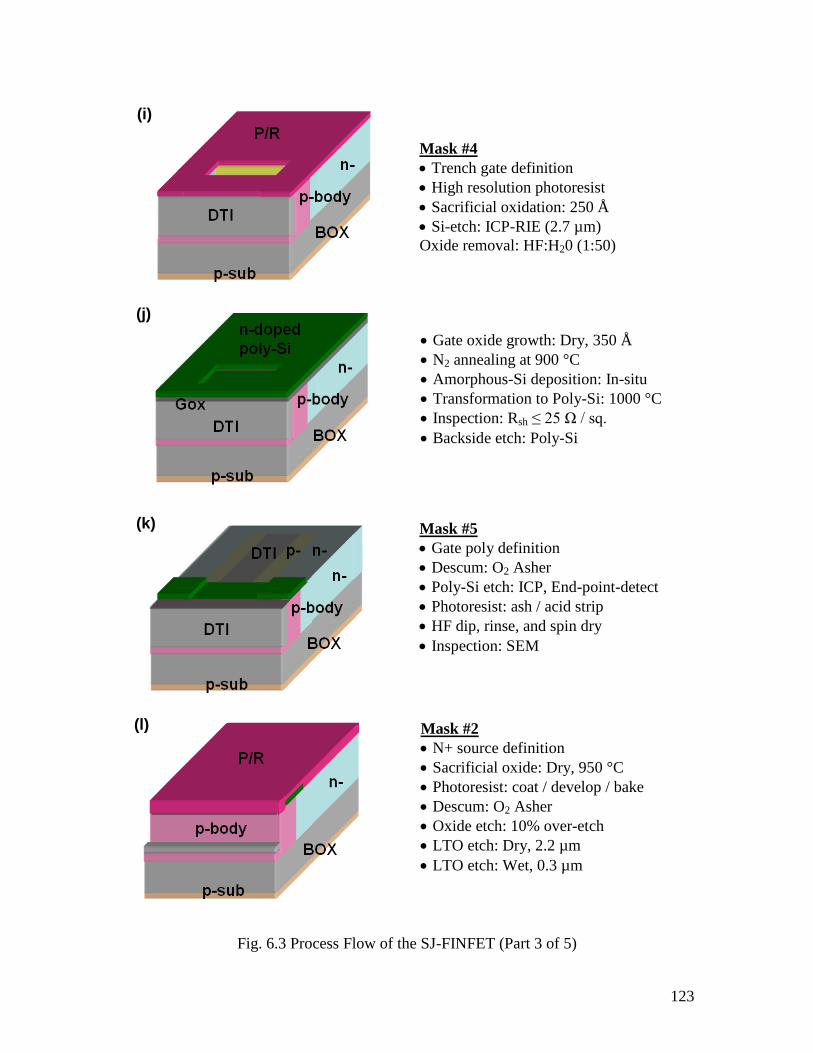
123
Fig. 6.3 Process Flow of the SJ-FINFET (Part 3 of 5)
(i)
(j)
(k)
(l)
Mask #4
Trench gate definition
High resolution photoresist
Sacrificial oxidation: 250 Å
Si-etch: ICP-RIE (2.7 µm)
Oxide removal: HF:H20 (1:50)
Gate oxide growth: Dry, 350 Å
N2 annealing at 900 °C
Amorphous-Si deposition: In-situ
Transformation to Poly-Si: 1000 °C
Inspection: Rsh ≤ 25 Ω / sq.
Backside etch: Poly-Si
Mask #5
Gate poly definition
Descum: O2 Asher
Poly-Si etch: ICP, End-point-detect
Photoresist: ash / acid strip
HF dip, rinse, and spin dry
Inspection: SEM
Mask #2
N+ source definition
Sacrificial oxide: Dry, 950 °C
Photoresist: coat / develop / bake
Descum: O2 Asher
Oxide etch: 10% over-etch
LTO etch: Dry, 2.2 µm
LTO etch: Wet, 0.3 µm
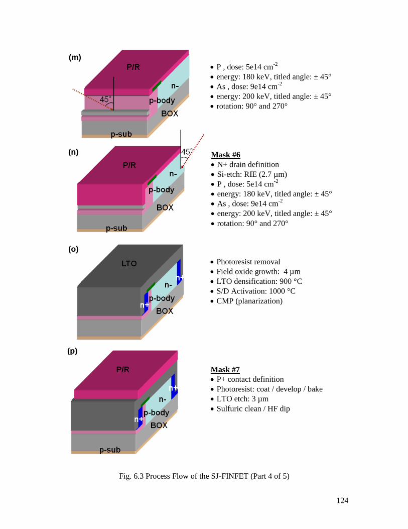
124
Fig. 6.3 Process Flow of the SJ-FINFET (Part 4 of 5)
(m)
(n)
(o)
(p)
P , dose: 5e14 cm-2
energy: 180 keV, titled angle: ± 45°
As , dose: 9e14 cm-2
energy: 200 keV, titled angle: ± 45°
rotation: 90° and 270°
Mask #6
N+ drain definition
Si-etch: RIE (2.7 µm)
P , dose: 5e14 cm-2
energy: 180 keV, titled angle: ± 45°
As , dose: 9e14 cm-2
energy: 200 keV, titled angle: ± 45°
rotation: 90° and 270°
Photoresist removal
Field oxide growth: 4 µm
LTO densification: 900 °C
S/D Activation: 1000 °C
CMP (planarization)
Mask #7
P+ contact definition
Photoresist: coat / develop / bake
LTO etch: 3 µm
Sulfuric clean / HF dip
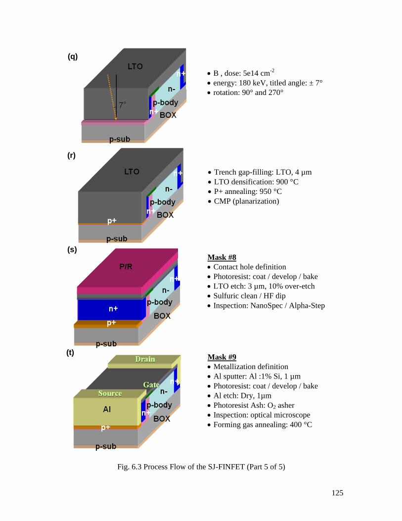
125
Fig. 6.3 Process Flow of the SJ-FINFET (Part 5 of 5)
(q)
(r)
(s)
(t)
B , dose: 5e14 cm-2
energy: 180 keV, titled angle: ± 7°
rotation: 90° and 270°
Trench gap-filling: LTO, 4 µm
LTO densification: 900 °C
P+ annealing: 950 °C
CMP (planarization)
Mask #8
Contact hole definition
Photoresist: coat / develop / bake
LTO etch: 3 µm, 10% over-etch
Sulfuric clean / HF dip
Inspection: NanoSpec / Alpha-Step
Mask #9
Metallization definition
Al sputter: Al :1% Si, 1 µm
Photoresist: coat / develop / bake
Al etch: Dry, 1µm
Photoresist Ash: O2 asher
Inspection: optical microscope
Forming gas annealing: 400 °C
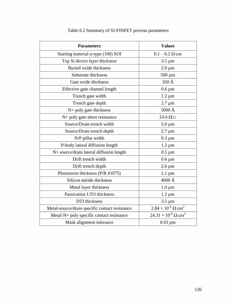
126
Table 6.2 Summary of SJ-FINFET process parameters
Parameters Values
Starting material n-type (100) SOI 0.1 – 0.2 Ω∙cm
Top Si device layer thickness 3.5 µm
Buried oxide thickness 2.0 µm
Substrate thickness 500 µm
Gate oxide thickness 350 Å
Effective gate channel length 0.6 µm
Trench gate width 1.2 µm
Trench gate depth 2.7 µm
N+ poly gate thickness 5000 Å
N+ poly gate sheet resistance 24.6 Ω/□
Source/Drain trench width 5.0 µm
Source/Drain trench depth 2.7 µm
N/P pillar width 0.3 µm
P-body lateral diffusion length 1.2 µm
N+ source/drain lateral diffusion length 0.5 µm
Drift trench width 0.6 µm
Drift trench depth 2.6 µm
Photoresist thickness (P/R #1075) 1.1 µm
Silicon nitride thickness 4000 Å
Metal layer thickness 1.0 µm
Passivation LTO thickness 1.2 µm
DTI thickness 3.5 µm
Metal-source/drain specific contact resistance 2.84 × 10⁻⁶
Ω∙cm2
Metal-N+ poly specific contact resistance 24.31 × 10⁻⁶
Ω∙cm2
Mask alignment tolerance 0.03 µm
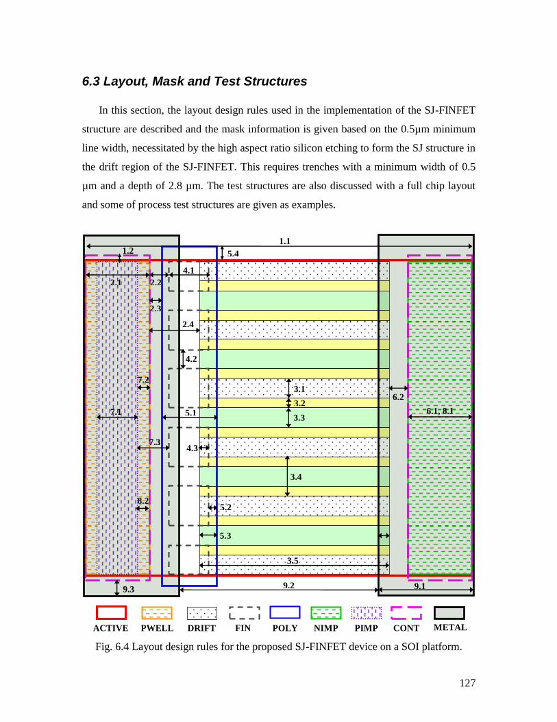
127
6.3 Layout, Mask and Test Structures
In this section, the layout design rules used in the implementation of the SJ-FINFET
structure are described and the mask information is given based on the 0.5µm minimum
line width, necessitated by the high aspect ratio silicon etching to form the SJ structure in
the drift region of the SJ-FINFET. This requires trenches with a minimum width of 0.5
µm and a depth of 2.8 µm. The test structures are also discussed with a full chip layout
and some of process test structures are given as examples.
Fig. 6.4 Layout design rules for the proposed SJ-FINFET device on a SOI platform.
METAL ACTIVE PWELL DRIFT FIN POLY NIMP PIMP CONT
1.1 1.2
2.1 2.2
2.3
2.4
3.1
3.2
3.3
3.4
3.5
4.1
4.2
4.3
5.1
5.2
5.3
6.1, 8.1
6.2
7.1
7.3
7.2
8.2
9.1 9.2
5.4
9.3

128
Defining design rules involves the consideration of factors such as the lateral
diffusion, minimum device area and maximum misalignment of the equipment. Mask
alignment error can be defined as the mask alignment tolerance (0.03 µm for ASML
Stepper 5000) multiplied by the square root of the number of alignment steps. In this
design, a minimum line width of 0.5 µm and an alignment tolerance of 0.1 µm were used.
The layout design rules for the low voltage SJ-FINFET devices are illustrated in Fig. 6.4
and summarized in Table 6.3.
Table 6.3 Summary of SJ-FINFET layout design rules
Mask Layout
Rule No. Description
Dimension
(µm)
ACTIVE 1.1 Minimum width 12.2
1.2 Minimum clearance to contact opening 0.3
PWELL
2.1 Minimum width 3.6
2.2 Minimum clearance to trench gate 0.6
2.3 Minimum clearance to gate poly 0.5
2.4 Minimum clearance to drift edge 1.4
DRIFT
3.1 Minimum width of drift trench 0.5
3.2 Minimum p-pillar diffusion length 0.25
3.3 Minimum spacing between p-pillars 0.6
3.4 Minimum spacing between drift trenches 1.2
3.5 Minimum length of drift trench 3.0
FIN
4.1 Minimum width 0.9
4.2 Minimum spacing between trench gates 0.6
4.3 Minimum overlap between FIN and DRFIT 0.1
POLY
5.1 Minimum width 1.4
5.2 Minimum overlap between FIN and POLY 0.1
5.3 Minimum overlap between POLY and drift edge 0.2
5.4 Minimum extension of poly to active 0.5
NIMP 6.1 Minimum width 3.6
6.2 Minimum clearance to drift edge 0.6
PIMP
7.1 Minimum width 3.6
7.2 Minimum overlap between PWELL and PIMP 0.6
7.3 Minimum clearance to trench gate 1.5
CONT 8.1 Minimum width 3.6
8.2 Minimum overlap between PIMP and CONT 0.6
METAL
9.1 Minimum width 5.0
9.2 Minimum spacing between metal lines 5.0
9.3 Minimum overlap between CONT and METAL 0.5

129
Instead of a conventional contact aligner which loads the mask directly in contact
with the substrate and exposes the photoresist, a 5× i-line (λ=365nm) stepper was used as
a photolithography tool for a better resolution and tolerance. This corresponds to the fact
that the feature size on the mask will be five times larger than the drawn layout size. The
SJ-FINFET fabrication requires a total of nine masking layers and the mask information
is as summarized in Table 6.4.
Table 6.4 SJ-FINFET Mask Information
Mask Layer Description Polarity (layer #)
1. ACTIVE Active and Isolation (DTI) Clear (3)
2. PWELL Trench for p-body & n+ source Dark (237)
3. DRIFT Trench for p-drift region formation Dark (63)
4. FIN Trench gate formation Dark (4)
5. POLY Polysilicon gate formation Clear (13)
6. NIMP Trench for n+ drain region Dark (8)
7. PIMP Trench for p+ contact Dark (7)
8. CONT Contact openings Dark (15)
9. METAL Al-Metallization Clear (16)
The entire test chip layout is as illustrated in Fig. 6.5. The total area of the layout is
100,000 µm 100,000 µm (or 500,000 µm 500,000 µm for the mask). The test chip
contains various process and device test structures of different sizes. It consists of six
groups of test elements (A-F):
(A) This group includes a large inter-digitated (i.e. multi-finger) SJ-FINFET structure
with a total gate width of 111,600 µm.

130
(B) This group includes a large inter-digitated SJ-LDMOS structure with a total gate
width of 111,600 µm for a comparison purpose.
(C) This group includes various single and multi-finger SJ-FINFET and SJ-LDMOS
structures for different gate width (10, 20, 40, 80, 100, and 200 µm) and SJ-
diodes with different drift lengths (3.5, 4.5, 6, 8, 10, and 12µm). Each device has
connected to the test pads with size of 100 µm 100 µm for DC measurement.
(D) This group includes several multi-finger SJ-FINFET (W = 200 µm) structures for
different n/p width ratios (0.67, 1.00, 1.33, and 1.67) and SJ-drift trench widths
(0.6, 0.8, 1.0, and 1.2). They are also subdivided into different drift length for a
comparison purpose.
(E) This group includes several multi-finger SJ-FINFET (W = 200 µm) structures for
different source/drain trench width (3.6 - 5µm), gate length (1-1.8µm with a 0.1
µm increment), and field plate length (0.1-0.9 with a 0.1 µm increment). Also, it
contains the test structures for contact resistance, sheet resistance (a Kelvin cross
with 6 terminals), and open/short circuit (i.e. leakage current) measurements of
the various layers.
(F) Lastly, this group includes various process test structures required for film
thickness, step height and coverage (i.e. monitoring etching) measurements. The
alignment marks and critical dimension (e.g. SEM inspection) structures are also
included as illustrated in Fig. 6.6.
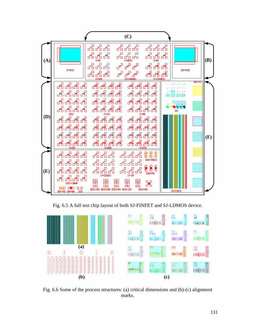
131
Fig. 6.5 A full test chip layout of both SJ-FINFET and SJ-LDMOS device.
Fig. 6.6 Some of the process structures: (a) critical dimensions and (b)-(c) alignment
marks.
(c) (b)
(a)
(A)
(D)
(E)
(B)
(C)
(F)
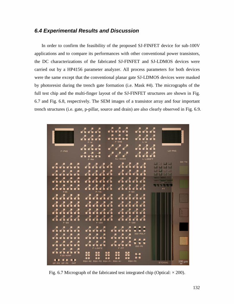
132
6.4 Experimental Results and Discussion
In order to confirm the feasibility of the proposed SJ-FINFET device for sub-100V
applications and to compare its performances with other conventional power transistors,
the DC characterizations of the fabricated SJ-FINFET and SJ-LDMOS devices were
carried out by a HP4156 parameter analyzer. All process parameters for both devices
were the same except that the conventional planar gate SJ-LDMOS devices were masked
by photoresist during the trench gate formation (i.e. Mask #4). The micrographs of the
full test chip and the multi-finger layout of the SJ-FINFET structures are shown in Fig.
6.7 and Fig. 6.8, respectively. The SEM images of a transistor array and four important
trench structures (i.e. gate, p-pillar, source and drain) are also clearly observed in Fig. 6.9.
Fig. 6.7 Micrograph of the fabricated test integrated chip (Optical: × 200).
100 µm
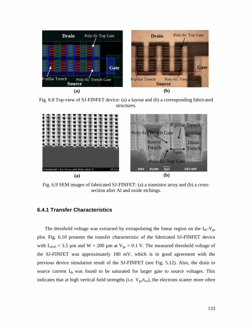
133
Fig. 6.8 Top-view of SJ-FINFET device: (a) a layout and (b) a corresponding fabricated
structures.
Fig. 6.9 SEM images of fabricated SJ-FINFET: (a) a transistor array and (b) a cross-
section after Al and oxide etchings.
6.4.1 Transfer Characteristics
The threshold voltage was extracted by extrapolating the linear region on the Ids-Vgs
plot. Fig. 6.10 presents the transfer characteristic of the fabricated SJ-FINFET device
with Ldrift = 3.5 µm and W = 200 µm at Vgs = 0.1 V. The measured threshold voltage of
the SJ-FINFET was approximately 180 mV, which is in good agreement with the
previous device simulation result of the SJ-FINFET (see Fig. 5.12). Also, the drain to
source current Ids was found to be saturated for larger gate to source voltages. This
indicates that at high vertical field strengths (i.e. Vgs/tox), the electrons scatter more often
(a) (b)
P-pillar Trench
Source
Trench Drain
Trench
Poly-Si: Top Gate
Ldrift
Poly-Si: Trench Gate
P-pillar Trench
Source
Poly-Si: Top Gate Drain
(a)
Poly-Si: Trench Gate
(b)
Gate
Drain
Source
Gate
Poly-Si: Top Gate
Poly-Si: Trench Gate P-pillar Trench
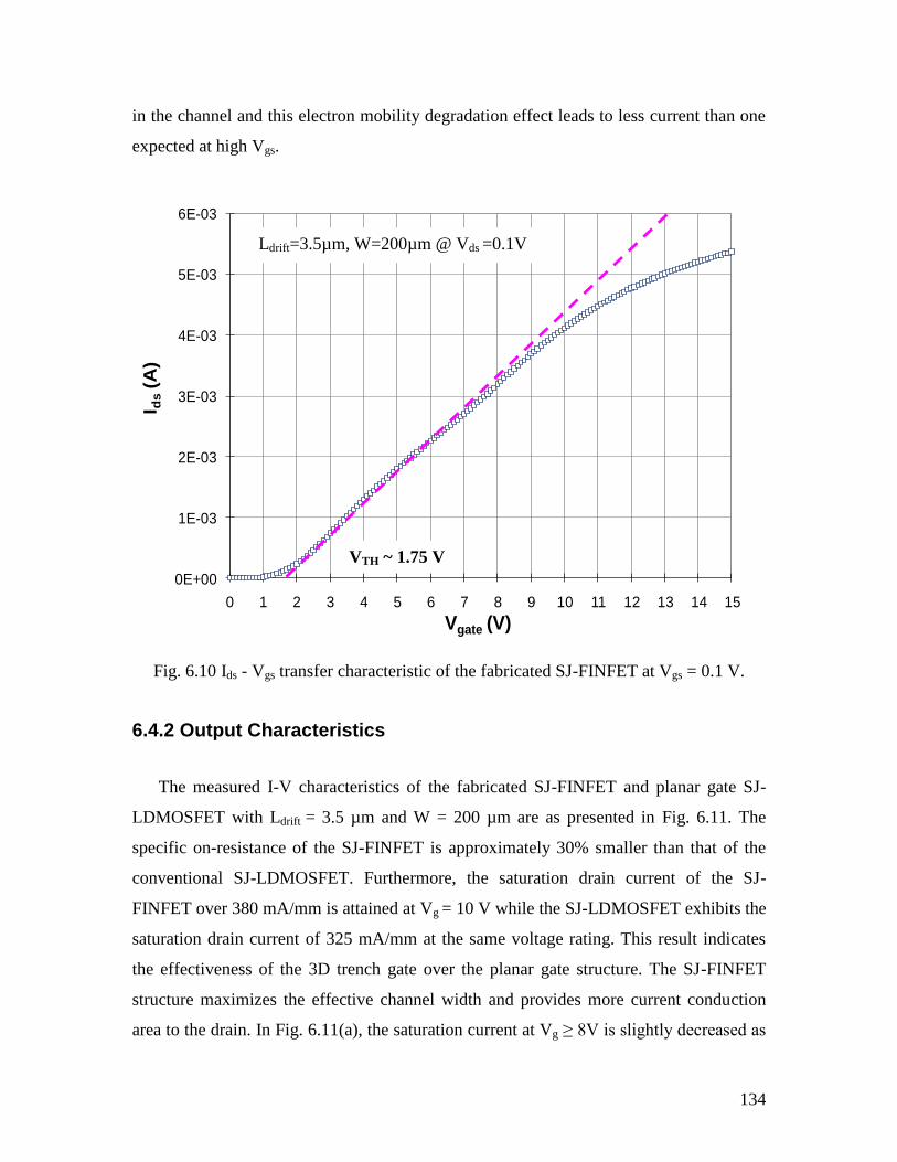
134
in the channel and this electron mobility degradation effect leads to less current than one
expected at high Vgs.
Fig. 6.10 Ids - Vgs transfer characteristic of the fabricated SJ-FINFET at Vgs = 0.1 V.
6.4.2 Output Characteristics
The measured I-V characteristics of the fabricated SJ-FINFET and planar gate SJ-
LDMOSFET with Ldrift = 3.5 µm and W = 200 µm are as presented in Fig. 6.11. The
specific on-resistance of the SJ-FINFET is approximately 30% smaller than that of the
conventional SJ-LDMOSFET. Furthermore, the saturation drain current of the SJ-
FINFET over 380 mA/mm is attained at Vg = 10 V while the SJ-LDMOSFET exhibits the
saturation drain current of 325 mA/mm at the same voltage rating. This result indicates
the effectiveness of the 3D trench gate over the planar gate structure. The SJ-FINFET
structure maximizes the effective channel width and provides more current conduction
area to the drain. In Fig. 6.11(a), the saturation current at Vg ≥ 8V is slightly decreased as
0E+00
1E-03
2E-03
3E-03
4E-03
5E-03
6E-03
0 1 2 3 4 5 6 7 8 9 10 11 12 13 14 15
I ds
(A)
Vgate (V)
Ldrift=3.5µm, W=200µm @ Vds =0.1V
VTH ~ 1.75 V
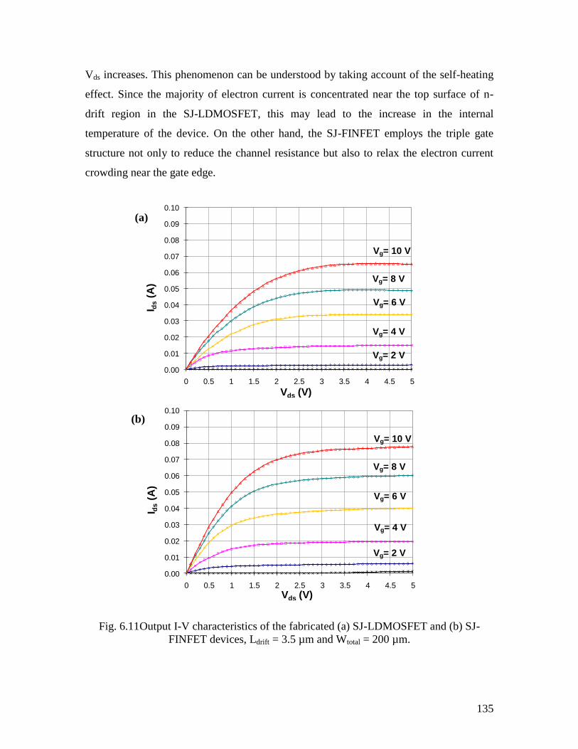
135
Vds increases. This phenomenon can be understood by taking account of the self-heating
effect. Since the majority of electron current is concentrated near the top surface of n-
drift region in the SJ-LDMOSFET, this may lead to the increase in the internal
temperature of the device. On the other hand, the SJ-FINFET employs the triple gate
structure not only to reduce the channel resistance but also to relax the electron current
crowding near the gate edge.
Fig. 6.11Output I-V characteristics of the fabricated (a) SJ-LDMOSFET and (b) SJ-
FINFET devices, Ldrift = 3.5 µm and Wtotal = 200 µm.
0.00
0.01
0.02
0.03
0.04
0.05
0.06
0.07
0.08
0.09
0.10
0 0.5 1 1.5 2 2.5 3 3.5 4 4.5 5
I ds
(A)
Vds (V)
0.00
0.01
0.02
0.03
0.04
0.05
0.06
0.07
0.08
0.09
0.10
0 0.5 1 1.5 2 2.5 3 3.5 4 4.5 5
I ds
(A)
Vds (V)
(a)
(b)
Vg= 2 V
Vg= 4 V
Vg= 6 V
Vg= 8 V
Vg= 10 V
Vg= 2 V
Vg= 4 V
Vg= 6 V
Vg= 8 V
Vg= 10 V
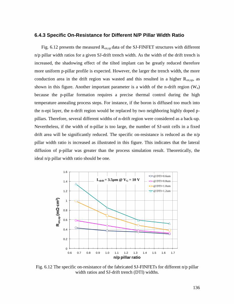
136
6.4.3 Specific On-Resistance for Different N/P Pillar Width Ratio
Fig. 6.12 presents the measured Ron,sp data of the SJ-FINFET structures with different
n/p pillar width ratios for a given SJ-drift trench width. As the width of the drift trench is
increased, the shadowing effect of the tilted implant can be greatly reduced therefore
more uniform p-pillar profile is expected. However, the larger the trench width, the more
conduction area in the drift region was wasted and this resulted in a higher Ron,sp, as
shown in this figure. Another important parameter is a width of the n-drift region (Wn)
because the p-pillar formation requires a precise thermal control during the high
temperature annealing process steps. For instance, if the boron is diffused too much into
the n-epi layer, the n-drift region would be replaced by two neighboring highly doped p-
pillars. Therefore, several different widths of n-drift region were considered as a back-up.
Nevertheless, if the width of n-pillar is too large, the number of SJ-unit cells in a fixed
drift area will be significantly reduced. The specific on-resistance is reduced as the n/p
pillar width ratio is increased as illustrated in this figure. This indicates that the lateral
diffusion of p-pillar was greater than the process simulation result. Theoretically, the
ideal n/p pillar width ratio should be one.
Fig. 6.12 The specific on-resistance of the fabricated SJ-FINFETs for different n/p pillar
width ratios and SJ-drift trench (DTI) widths.
0
0.2
0.4
0.6
0.8
1
1.2
1.4
1.6
0.6 0.7 0.8 0.9 1.0 1.1 1.2 1.3 1.4 1.5 1.6 1.7
Ro
n,s
p(m
Ω∙c
m2)
n/p pillar ratio
@ DTI=0.6um
@ DTI=0.8um
@ DTI=1.0um
@ DTI=1.2um
Ldrift = 3.5µm @ VG = 10 V

137
6.4.4 Breakdown Voltage for Different SJ-drift Regions
The operating principle of the SJ device is based on charge compensation. The charge
imbalance between n-drift and p-drift layers directly affects the value of BV. Thus, it is
important to evaluate the effect of charge imbalance in order to achieve the maximum BV.
Fig. 6.13 presents the relationship between BV and p-pillar dose. Since the n-pillar
doping concentration is fixed (i.e. n-epi device layer), the variation of p-pillar dose has
the same effect of giving different charge balance conditions in the SJ-drift region. It can
be seen that the optimal breakdown voltage is obtained at the p-pillar dose of 8 ×
1013
/cm2. This can be explained by the fact that the cross-sectional areas of n-/p- pillars
are different from each other; therefore the ND and NA should be also different. In this
figure, the BV of SJ-FINFET is highly sensitive to the p-pillar or charge imbalance (%)
in the pillars. If charge imbalance between the pillars exists, the gradient of the electric
field in the drift region is proportional to the pillars doping concentrations for a specific
charge imbalance (%) with the resultant p-p-n+ (for NA > ND) or p-n-n
+ (for ND > NA)
diode having effectively highly doped drift region. Such high sensitivity imposes
stringent requirements for a precisely controlled fabrication process.
Fig. 6.13 The relationship between BV and P-pillar dose for the fabricated SJ-FINFET
devices with Ldrift of 3.5 µm and 6 µm, Wn = Wp = 0.3 µm and Wside of 2.7 µm.
0
20
40
60
80
100
3.0E+13 5.0E+13 7.0E+13 9.0E+13 1.1E+14
BV
(V
)
P-pillar Dose (cm-2)
Wside / Ldrift = 2.7µm / 6.0µm
Wside / Ldrift = 2.7µm / 3.5µm
B, 8e13 cm-2, 45keV, 12
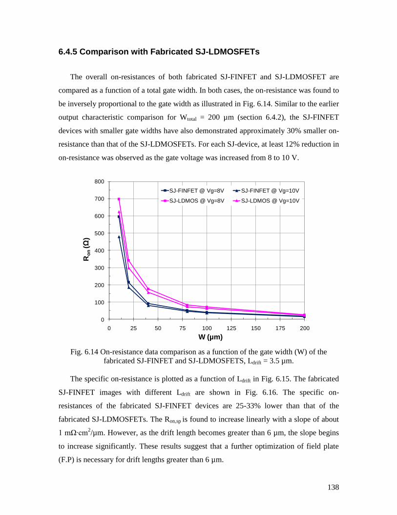
138
6.4.5 Comparison with Fabricated SJ-LDMOSFETs
The overall on-resistances of both fabricated SJ-FINFET and SJ-LDMOSFET are
compared as a function of a total gate width. In both cases, the on-resistance was found to
be inversely proportional to the gate width as illustrated in Fig. 6.14. Similar to the earlier
output characteristic comparison for Wtotal = 200 µm (section 6.4.2), the SJ-FINFET
devices with smaller gate widths have also demonstrated approximately 30% smaller on-
resistance than that of the SJ-LDMOSFETs. For each SJ-device, at least 12% reduction in
on-resistance was observed as the gate voltage was increased from 8 to 10 V.
Fig. 6.14 On-resistance data comparison as a function of the gate width (W) of the
fabricated SJ-FINFET and SJ-LDMOSFETS, Ldrift = 3.5 µm.
The specific on-resistance is plotted as a function of Ldrift in Fig. 6.15. The fabricated
SJ-FINFET images with different Ldrift are shown in Fig. 6.16. The specific on-
resistances of the fabricated SJ-FINFET devices are 25-33% lower than that of the
fabricated SJ-LDMOSFETs. The Ron,sp is found to increase linearly with a slope of about
1 mΩ∙cm2/µm. However, as the drift length becomes greater than 6 µm, the slope begins
to increase significantly. These results suggest that a further optimization of field plate
(F.P) is necessary for drift lengths greater than 6 µm.
0
100
200
300
400
500
600
700
800
0 25 50 75 100 125 150 175 200
Ro
n(Ω
)
W (µm)
SJ-FINFET @ Vg=8V SJ-FINFET @ Vg=10V
SJ-LDMOS @ Vg=8V SJ-LDMOS @ Vg=10V
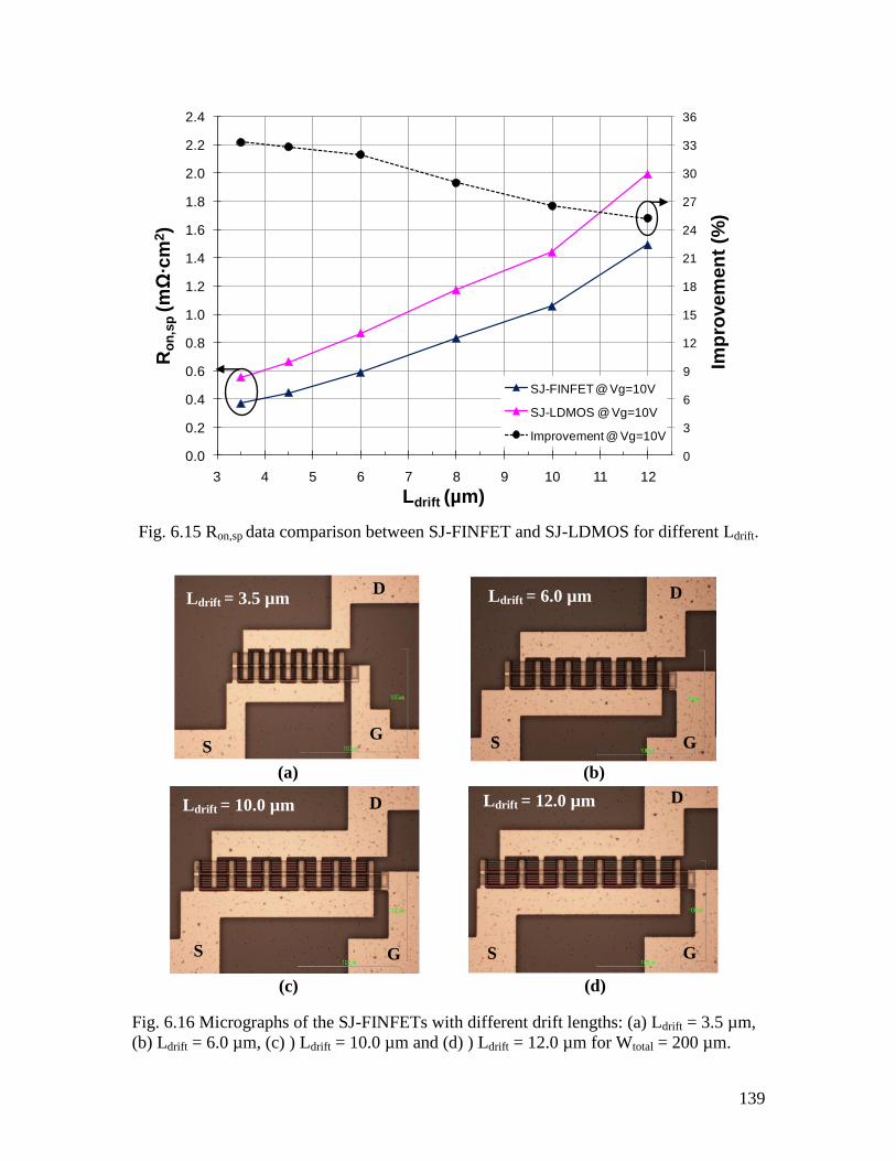
139
Fig. 6.15 Ron,sp data comparison between SJ-FINFET and SJ-LDMOS for different Ldrift.
Fig. 6.16 Micrographs of the SJ-FINFETs with different drift lengths: (a) Ldrift = 3.5 µm,
(b) Ldrift = 6.0 µm, (c) ) Ldrift = 10.0 µm and (d) ) Ldrift = 12.0 µm for Wtotal = 200 µm.
0
3
6
9
12
15
18
21
24
27
30
33
36
0.0
0.2
0.4
0.6
0.8
1.0
1.2
1.4
1.6
1.8
2.0
2.2
2.4
3 4 5 6 7 8 9 10 11 12
Imp
rovem
en
t (%
)
Ro
n,s
p(m
Ω∙c
m2)
Ldrift (µm)
SJ-FINFET @ Vg=10V
SJ-LDMOS @ Vg=10V
Improvement @ Vg=10V
(a) (b)
(d) (c)
Ldrift = 3.5 µm Ldrift = 6.0 µm
Ldrift = 10.0 µm Ldrift = 12.0 µm
G S
D
G S
D
G S
D
G S
D
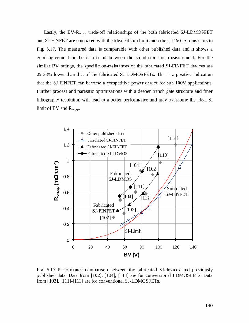
140
Lastly, the BV-Ron,sp trade-off relationships of the both fabricated SJ-LDMOSFET
and SJ-FINFET are compared with the ideal silicon limit and other LDMOS transistors in
Fig. 6.17. The measured data is comparable with other published data and it shows a
good agreement in the data trend between the simulation and measurement. For the
similar BV ratings, the specific on-resistances of the fabricated SJ-FINFET devices are
29-33% lower than that of the fabricated SJ-LDMOSFETs. This is a positive indication
that the SJ-FINFET can become a competitive power device for sub-100V applications.
Further process and parasitic optimizations with a deeper trench gate structure and finer
lithography resolution will lead to a better performance and may overcome the ideal Si
limit of BV and Ron,sp.
Fig. 6.17 Performance comparison between the fabricated SJ-devices and previously
published data. Data from [102], [104], [114] are for conventional LDMOSFETs. Data
from [103], [111]-[113] are for conventional SJ-LDMOSFETs.
Si-
Limi
t
0
0.2
0.4
0.6
0.8
1
1.2
1.4
0 20 40 60 80 100 120 140
Ro
n,s
p(m
Ω∙c
m2 )
BV (V)
Other published data
Simulated SJ-FINFET
Fabricated SJ-FINFET
Fabricated SJ-LDMOS
Simulated
SJ-FINFET
Si-Limit
Fabricated
SJ-FINFET
Fabricated
SJ-LDMOS
[102]
[104]
[103]
[104] [102]
[111]
[112]
[113]
[114]
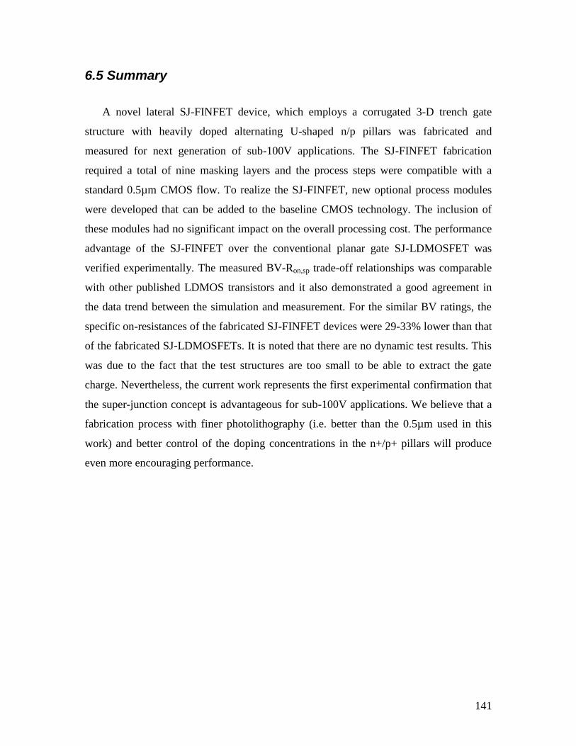
141
6.5 Summary
A novel lateral SJ-FINFET device, which employs a corrugated 3-D trench gate
structure with heavily doped alternating U-shaped n/p pillars was fabricated and
measured for next generation of sub-100V applications. The SJ-FINFET fabrication
required a total of nine masking layers and the process steps were compatible with a
standard 0.5µm CMOS flow. To realize the SJ-FINFET, new optional process modules
were developed that can be added to the baseline CMOS technology. The inclusion of
these modules had no significant impact on the overall processing cost. The performance
advantage of the SJ-FINFET over the conventional planar gate SJ-LDMOSFET was
verified experimentally. The measured BV-Ron,sp trade-off relationships was comparable
with other published LDMOS transistors and it also demonstrated a good agreement in
the data trend between the simulation and measurement. For the similar BV ratings, the
specific on-resistances of the fabricated SJ-FINFET devices were 29-33% lower than that
of the fabricated SJ-LDMOSFETs. It is noted that there are no dynamic test results. This
was due to the fact that the test structures are too small to be able to extract the gate
charge. Nevertheless, the current work represents the first experimental confirmation that
the super-junction concept is advantageous for sub-100V applications. We believe that a
fabrication process with finer photolithography (i.e. better than the 0.5µm used in this
work) and better control of the doping concentrations in the n+/p+ pillars will produce
even more encouraging performance.

142
Chapter 7 Conclusions
In this thesis, the development and experimental verification of the next generation
low-voltage power MOSFETs have been described. In the first part of the thesis, the
feasibility of monolithic integration of a high speed, high efficiency buck converter was
investigated in terms of the layout optimization. In particular, the unit-cell structure of the
hybrid waffle (HW) layout, implemented in a 0.25µm, 5 metal layer standard CMOS
process was optimized for minimum specific on-resistance with enhanced switching
characteristics. Analytical layout models containing parasitic resistors and capacitors
were proposed. This allowed more accurate power loss calculations for the final output
stage design. The HW layout technique organized MOSFET fingers in a square grid
arrangement. It was designed to provide an effective trade-off between the width of
diagonal source/drain metal and the active device area, allowing more effective
optimization between switching and conduction losses. In comparison with conventional
layout schemes, the HW layout was found to exhibit a 30% reduction in overall on-
resistance with 3.6 times smaller total gate charge for CMOS devices with a current
rating of 1A. The performance improvement was obtained with no processing or device
structural changes. The measured overall on-resistances for both the n- and p-type HW
power MOSFETs were in good agreement with the simulation results. Also, the
maximum measured efficiencies of the converter switching at 6.25 MHz and 10MHz
were 85% and 82%, respectively.
The focus of the second part of this thesis was to explore the suitability of the super-
junction (SJ) concept in low voltage power MOSFETs. Conventional SJ devices do not
have significant advantages over LDMOS devices in sub-100V rating applications. This
is due to the fact that the channel resistance becomes comparable to the drift region
resistance. A lateral super-junction FINFET (SJ-FINFET) with a corrugated 3-D trench
gate was presented to resolve this issue. Using highly doped alternating ultra thin n/p
pillars (the FINs) as the SJ drift region, the proposed devices could provide a new degree
of freedom in the trade-off between on-resistance and breakdown voltage. Three-
dimensional numerical simulations using ISE-DESSISTM
was performed to analyze the

143
effect of various device parameters. Several prototype devices were fabricated in a 0.5µm
CMOS process with nine masking layers. In comparison with conventional planar gate
SJ-LDMOSFETs, the fabricated SJ-FINFETs demonstrated approximately 30%
improvement in Ron,sp. This is a positive indication that the SJ-FINFET can become a
competitive power device for sub-100V applications. Further process and parasitic
optimizations with a deeper trench gate structure and finer lithography resolution will
lead to a better performance and may overcome the ideal Si limit of BV and Ron,sp.
Future work may take advantage of new developments in interconnects and contact
processes by incorporating Cu interconnects to reduce de-biasing effects and make use of
borderless contacts to increase the packing density. Consideration can be also given to
reduce the gate resistance using special silicide materials and new layout techniques to
further reduce the chip area for a given current carrying capability. Other future work
may consider modifying the existing process flow of the SJ-FINFET to achieve better
control of the doping concentrations between the pillars. In addition, the fabrication
process of the SJ-FINFET with finer photolithography should be considered in
combination with the HW layout strategy.

144
References:
[1] B. E. Taylor, Power MOSFET Design, New York: John Wiley, 1993.
[2] P. Antogentti, Power Integrated Circuits: Physics, Design, and Applications, New
York : McGraw-Hill, 1986.
[3] A. Hastings, The Art of Analog Layout, 2nd
ed., Upper Saddle River, NJ:
Pearson/Prentice Hall, 2006.
[4] D. A. Grant and J. Gowon, Power MOSFET Theory and Applications, New York:
John Wiley, Interscience, 1989.
[5] G. Majumdar, Future of Power Semiconductors, IEEE Power Electronics
Specialists Conference, pp.10-14, 2004.
[6] G. Hall and et al., SCR Manual, 1st ed., General Electric Co., Auburn, NY, 1958.
[7] M. Darwish and K. Board, LATERAL RESERFED COMFET, Electronics Letters,
pp. 519-520, 1984.
[8] S. Colak, B. Singer, and E. Stupp, Lateral DMOS Power Transistor Design, IEEE
Electron Device Letters, pp. 51–53, 1980.
[9] Y. Tarui, Y. Hayashi, and T. Sekigawa, Diffusion Self-aligned MOST: A New
Approch for High Speed Device, Suppl. to J. Japan Soc. of Appl. Phys., 39, pp.
105, 1970.
[10] D. Ueda, H. Takagi, A. Shimano, and G. Kano, A New Vertical Sidewall
Channel Power MOSFET with Rectangular Grooves, 16th Int. Conf. Solid-State
Devices and Materials, pp. 313, 1984.
[11] T. Fujihira, Theory of Semiconductor Superjunction Devices, Jpn. J. Appl. Phys.,
Vol. 36, pp. 6254, 1997.
[12] B.J. Baliga, M. S. Adler, P.V. Gray, and R.P. Love, The Insulated Gated Rectifier
(IGR): A New Power Switching Device, IEDM Tech. Digest, pp. 264-267, 1982.
[13] H.R. Chang, B.J. Baliga, J.W. Kretchmer, and P.A. Piacente, Insulated Gate
Bipolar Transistor (IGBT) with a Trench Gate Structure, IEDM Tech. Digest, pp.
674-677, 1987.

145
[14] G. Miller and J. sack, A New Concept for A Non Punch Through IGBT with
MODFET Like Switching Characteristics, IEEE Power Electronics Specialists
Conference, R1, pp. 21-25, 1989.
[15] T. Laska, M. Munzer, F. Pfirsch, C. Scheffer, and T. Schmidt, The Field-Stop
IGBT (FS IGBT) - A New Power Device Concept with A Great. Improvement
Potential, ISPSD‟00 Proceedings, pp. 355-358, 2000.
[16] M. Vukicevic, Data Processing Market to Dominate Power Semiconductor
Market in 2007: Market Tracker, iSuppli Corp., Q1, 2007.
[17] H. Shichman and D.A. Hodges, Modeling and Simulation of Integrated-Gate
Field-Effect Transistor Switching Circuits, IEEE J. Solid-State Circuits, Vol. SC-
3, pp.285-289, 1968.
[18] Y. Katayama, M. Edo, T. Denta, T. Kawashima, and T. Ninomiya, Optimum
Design Method of CMOS IC for DC-DC Converter that integrates Power Stage
MOSFETs, IEEE Power Electronics Specialists Conference, pp. 4486-4491, 2004.
[19] Z. J. Shen, D. N. Okada, F. Lin, S. Anderson, and X. Cheung, Lateral Power
MOSFET for Megahertz-Frequency, High-Density DC/DC Converters, IEEE
Trans. Power Electronics, Vol.21, No.1, pp.11-17, 2006.
[20] Z. J. Shen, A. Masrur, V. Garg and J. Monroe, Automotive Electric Power and
Energy Management – A System Approach, Global Automotive Manufacturing
and Technology, April, 2003.
[21] M.J. Gielniak and Z. J. Shen, Power Management Strategy Based on Game
Theory for Fuel Cell Hybrid Electric Vehicles, IEEE Vehicular Technology
Conference, Vol.6, pp 4422-4426, 2004.
[22] T. Kachi, GaN power Devices for Automotive Applications, IEEE Compound
Semiconductor IC Symposium, pp.1-4, 2007.
[23] J.W. Palmour, R. Singh, R.C. Glass, O. Kordina, and C.H. Carter, Silicon Carbide
for Power Devices, IEEE Power Semiconductor Devices and IC‟s, pp.25-32, 1997.
[24] H.R. Chang, E. Hanna, and A.V. Radun, Development and Demonstration of
Silicon Carbide Motor Drive Inverter Modules, IEEE Power Electronics
Specialist Conference, Vol.1, pp.15-19, 2003.
146
[25] T. Funaki, M. Matsushita, M. Sasagawa, T. Kimoto, and T. Hikihara, A Study on
SiC Devices in Synchronous Rectification of DC-DC Converter, IEEE Applied
Power Electronics Conference, pp.339-344, 2007.
[26] H. Kambayashi, Y. Niiyama, S. Ootomo, T. Nomura, M. Iwami, Y. Satoh, S.
Kato, and S. Yoshida, Normally Off n-Channel GaN MOSFETs on Si Substrates
Using an SAG Technique and Ion Implantation, IEEE Electron Device Letters,
vol. 28, no.12, pp. 1077-1079, 2007.
[27] C. S. Suh, Y. Dora, N. Fichtenbaum, L. McCarthy, S. Keller, and U. K. Mishra,
High-Breakdown Enhancement-Mode AlGaN/GaN HEMTs with Integrated Slant
Field-Plate, IEDM Tech Dig., pp.911-913, 2006.
[28] T. Morita, M. Yanagihara, H. Ishida, M. Hikita, K. Kaibara, H. Matsuo, Y.
Uemoto, T. Ueda, T. Tanaka, and D. Ueda, 650V 3.1mΩcm2 GaN-based
Monolithic Bidrectional Switch Using Normally-Off Gate Injection Transistor,
IEDM Tech Dig., pp.865-868, 2007.
[29] M. Sugimoto, H. Ueda, M. Kanechika, N. Soejima, T. Uesugi, and T. Kachi,
Vertical device operation of AlGaN/GaN HEMTs on free-standing n-GaN
substrates, IEEE Power Conversion Conference, pp.368-372, 2007.
[30] W. Saito, M. Kuraguchi, Y. Takada, K. Tsuda, Y. Saito, I. Omura, and M.
Yamaguchi, Current Collapseless High-Voltage GaN-HEMT and its 50-W Boost
Converter Operation, IEDM Tech Dig., pp.869-872, 2007.
[31] T. Nanjo, M. Takeuchi, M. Suita, Y. Abe, T. Oishi, Y. Tokuda, and Y. Aoyagi,
Remarkable Breakdown Voltage Enhancement in AlGaN Channel HEMTs,
IEDM Tech Dig., pp.397-400, 2007.
[32] D.A. Neamen, Semiconductor Physics and Devices: Basic Principles 2ed., New
York : McGraw-Hill, 1997.
[33] S.C. Sun, and J.D. Plummer, Modeling of the On-resistance of LDMOS, VDMOS,
and VMOS Power Transistors, IEEE Transactions on Electron Devices, vol.27,
Issue2, pp.356-367, 1980.
[34] D. Ueda, H. Takagi and G. Kano, An Ultra-Low On-Resistance Power MOSFET
Fabricated by Using a Fully Self-Aligned Process, IEEE Transactions on Electron
Devices, pp.926-930, 1987.
147
[35] P. M. Shenoy, A. Bhalla and G. M. Dolny, Analysis of the Effect of Charge
Imbalance on the Static and Dynamic Characteristics of the Super Junction
MOSFET, ISPSD‟99 Proceedings, vol. 35, pp.99-102, 1999.
[36] J.A. Appels and H.M.J. Vaes, HV Thin Layer Devices (RESURF Devices),
IEDM‟79 Proceedings, pp.238-241, 1979.
[37] T. Efland, C.Y. Tsai, J. Erdeljac, J. Mitros, and L. Hutter, A performance
comparison between new reduced surface drain “RSD” LDMOS and RESURF
and conventional planar power devices rated at 20V, ISPSD‟97 Proceedings,
pp.185-188, 1997.
[38] J.A.V. der Pol, et al., A-BCD: An Economic 100V RESURF Silicon-On-Insulator
BCD Technology for Consumer and Automotive Applications, ISPSD‟00
Proceedings, pp.327-330, 2000.
[39] T. Kubota, K. Watanabe, K. Karouji, M. Ueno, Y. Kawaguchi, and A. Nakagawa,
Cost-Effective Approach in LDMOS with Partial 0.35µm Design into
Conventional 0.6µm Process, ISPSD‟03 Proceedings, pp.245-248, 2003.
[40] M. Darwish, Scaling Issue in Lateral Power MOSFETs, ISPSD‟98 Proceedings,
pp.329-332, 1998.
[41] A. Van den Bosch, M.S.J. Steyaert, and W.Sansen, A High-Density, Matched
Hexagonal Structure in Standard CMOS Technology for High-Speed Applications,
IEEE Trans. Semiconductor Manufacturing, Vol.13, Issue.2, pp.167-172, 2000.
[42] J.D. Plummer and J.D. Meindl, A Monolithic 200-V CMOS Analog Switch, IEEE
J. Solid-State Circuits, Vol.SC-11, 6, pp.809-817, 1976.
[43] Y. Chen, Y. Fu, X. Cheng, T.X. Wu, and Z.J. Shen, Modeling and Analysis of
Metal Interconnect Resistance of Power IC‟s, ISPSD‟07 Proceedings, pp.253-256,
2007.
[44] L. Baker, R. Currences, S. Law, M. Le, C. Lee, S.T. Lin, and M. Teene, A Waffle
Layout Technique Strengthens the ESD Hardness of the NMOS Output Transistor,
EOS/ESD Symp. Proc. EOS-11, pp.175-181, 1989.
[45] L. Lorenz, I. Zverev, A. Mittal and J. Hancock, CoolMOS – A New Approach
Toward System Miniaturization and Energy Saving, Industry Applications
Conference, vol.5, pp.2974-2981, 2000.
148
[46] D. J. Coe, High Voltage Semiconductor Device, U.S. Patent 4754310, 1988.
[47] X. Chen, Semiconductor Power Device with Alternating Conductivity type High-
Volt-age Breakdown Region, U.S Patent 5216275, 1993.
[48] J. Tihanyi, Power MOSFET, U.S Patent 5438215, 1995.
[49] L. Lorenz, G. Deboy, A. Knapp and M. Marz, COOLMOSTM
– a new milestone
in high voltage Power MOS, ISPSD‟99 Proceedings, pp.3-10, 1999.
[50] M. Saggio, D. Fagone and S. Musumeci, MDmeshTM
: innovative technology for
high voltage Power MOSFETs, ISPSD‟00 Proceedings, pp.65-68, 2000.
[51] T. Fujihira and Y. Miyasaka, Simulated Superior Performances of Semiconductor
Superjunction Devices, ISPSD‟98 Proceedings, pp.423-426, 1998.
[52] C. Tolksdorf, J. Schuize, I. Eisele and G. Deboy, Lateral Compensation Structures
Can Break the Silicon Limit, IEEE Power Electronics Specialists Conference,
pp.585-590, 2004.
[53] R. P. Zingg, New Benchmark for RESURF, SOI and Super-junction Power
Devices, ISPSD‟01 Proceedings, pp.343-346, 2001.
[54] M. Rub, M. Bar, G. Deml, H. Kapels, M. Schmitt, S. Sedlmaier, C. Tolksdorf and
A. Willmeroth, A 600V 8.7Ω∙mm2 Lateral Superjunction Transistor, ISPSD‟06
Proceedings, pp.1-4, 2006.
[55] W. Saito, I. Omura, S. Aida, S. Koduki, M. Izumisawa, H. Yoshioka, H. Okumura,
M. Yamaguchi and T. Ogura, A 15.5mΩ∙cm2 – 680V Superjunction MOSFET
Reduced On-Resistance by Lateral Pitch Narrowing, ISPSD‟06 Proceedings,
pp.300-303, 2006.
[56] C. Rochefort, R. van Dalen, N. Duhayon and W. Vandervorst, Manufacturing of
High Aspect-ratio p-n junction using Vapor Phase Doping for Application in
Multi-Resurf Devices, ISPSD‟02 Proceedings, pp.237-240, 2002.
[57] R. Van Dalen and C. Rochefort, Vertical multi-RESURF MOSFETs Exhibiting
Record Low Specific Resistance, IEEE International Electron Device Meeting,
pp.31.1.1-31.1.4, 2003.
[58] R. Van Dalen and C. Rochefort, Electrical Characterization of Vertical Vapor
Phase Doped RESURF MOSFETs, ISPSD‟04 Proceedings, pp.451-454, 2004.
149
[59] K. P. Gan, X. Yang, Y. C. Liang, G. S. Samudra and Y. Liu, A Simple
Technology for Superjunction Device Fabrication: Polyflanked VDMOSFET,
IEEE Electron Device Letters, vol.23, no.10, pp.627-629, 2002.
[60] S. Yamauchi, T. Shibata, S. Nogami, T. Yamaoka, Y. Hattori and H. Yamaguchi,
200V Superjunction MOSFET Fabricated by High Aspect Ratio Trench Filling,
ISPSD‟06 Proceedings, pp.63-66, 2006.
[61] T. Minato, T. Nitta, A. Uenisi, M. Yano, M. Harada and S. Hine, Which is cooler,
Trench or Multi-Epitaxy? Cutting edge approach for the Silicon limit by the Super
Trench power MOS-FET (STM), ISPSD‟00 Proceedings, pp.73-76. 2000.
[62] A. Sugi, M. Takei, K. Takahashi, A. Yajima, H. Tomizawa and H. Nakazawa,
Super Junction MOSFETs above 600V with Parallel Gate Structure Fabricated by
Deep Trench Etching and Epitaxial Growth, ISPSD‟08 Proceedings, pp.165-168,
2008.
[63] P. Moens, F. Bauwens, J. Baele, K. Vershinin, E. De Backer, E.M. Sankara
Narayanan and M. Tack, XtreMOSTM
: The First Integrated Power Transistor
Breaking the Silicon Limit, IEEE International Electron Device Meeting, pp.445-
449, 2006.
[64] Y. Chen, K.D. Buddharaju, Y.C. Liang, G.S. Samudra and H.H. Feng,
Superjunction Power LDMOS on Partial SOI Platform, ISPSD‟07 Proceedings,
pp.177-180, 2007.
[65] R. Zhu, V. Parthasarathy, V. Khemka and A. Bose, A 0.250Micron Smart Power
Technology Optimized for Wireless and Consumer Applications, ISPSD‟03
Proceedings, pp.178-181, 2003.
[66] F. Kawai, T. Onishi, T. kamiya, H. Ishimabushi, H. Eguchi, K. Nakahama, H.
Aoki and K. Hamada, Multi-Voltage SOI-BiCDMOS for 14V and 42V
Automotive Applications, ISPSD‟04 Proceedings, pp.165-168, 2004.
[67] T. Kubota, K. Watanabe, K. Karouji, M. Ueno, Y. Anai, Y. Kawaguchi and A.
Nakagawa, Cost-Effective Approach in LDMOS with Partial 0.35µm Design into
Conventional 0.6µm Process, ISPSD‟03 Proceedings, pp.245-248, 2003.

150
[68] V. Parthasarathy, V. Khemka, R. Zhu and A. Rose, SOA Improvement by a
Double RESURF LDMOS Technique in a Power IC Technology, IEEE
International Electron Device Meeting, pp.75-78, 2000.
[69] V. Khemka, V. Parthasarathy, R. Zhu, A. Bow and T. Roggenbauer, Floating
RESURF (FRESURF) LDMOSFET Devices with Breakthrough BVds-Rdson,
ISPSD‟04 Proceedings, pp.415-418, 2004.
[70] R. Ng, F. Udrea, K. Sheng, K. Ueno, G. A. J. Amaratunga and M. Nishiura,
Lateral Unbalanced Super Junction (USJ)/3D-RESURF for High Breakdown
Voltage on SOI, ISPSD‟01 Proceedings, pp.395-398, 2001.
[71] M. Daarwish, J. Huang, M. Liu, M. Shekar, R. Williams, M. Cornel, Scaling
Issues in Lateral Power MOSFETs, ISPSD‟98 Proceedings, pp.329-332, 1998.
[72] O. Trescases, W.T. Ng, H. Nishio, M. Edo, and T. Kawashima, A Digitally
Controlled DC-DC Converter Module with a Segmented Output Stage for
Optimized Efficiency, ISPSD‟06 Proceedings, pp.409-413, 2006.
[73] A. Yoo, M. Chang, O. Trescases, and W. T. Ng, High Performance Low-Voltage
Power MOSFETs with Hybrid Waffle Layout Structure in a 0.25µm Standard
CMOS Process, ISPSD‟08 Proceedings, pp.95-98, 2008.
[74] M. Chang, Multi-MHz Output Stage Design for Integrated DC-DC Converters,
MASc Thesis, University of Toronto, 2008.
[75] “Si5920DC Dual N-Channel 1.5-V (G-S) MOSFET,” Datasheet, Vishay Siliconix,
2007, available: http://www.vishay.com.
[76] “Si1450DH N-Channel 8-V (D-S) MOSFET,” Datasheet, Vishay Siliconix, 2006,
available: http://www.vishay.com.
[77] “Si8424DB N-Channel 1.2-V (G-S) MOSFET,” Datasheet, Vishay Siliconix,
2006, available: http://www.vishay.com.
[78] “SiA414DJ N-Channel 8-V (D-S) MOSFET,” Datasheet, Vishay Siliconix, 2007,
available: http://www.vishay.com.
[79] “Si1050X N-Channel 8-V (D-S) MOSFET,” Datasheet, Vishay Siliconix, 2006,
available: http://www.vishay.com.
[80] “Si8404DB N-Channel 1.5-V (G-S) MOSFET,” Datasheet, Vishay Siliconix,
2006, available: http://www.vishay.com.

151
[81] “MGSF1N02LT1 N-Channel SOT-23,” Datasheet, ON Semiconductor, 2005,
available: http://www.onsemi.com.
[82] “MMBF0201NLT1 N-Channel SOT-23,” Datasheet, ON Semiconductor, 2006,
available: http://www.onsemi.com.
[83] “NTA4153N Single N-Channel SC-75 and SC-89,” Datasheet, ON
Semiconductor, 2007, available: http://www.onsemi.com.
[84] “NTK3134N Single N-Channel with SOT-723,” Datasheet, ON Semiconductor,
2006, available: http://www.onsemi.com.
[85] S. L. Colino and S. P. Schultz, Figure of Merit for High-Frequency Switches,
Power Electronics Technology Exhibition & Conference, Oct. 2006.
[86] A. Yoo, M. Chang, O. Trescases, H. Wang, and W. T. Ng, FOM (Figure of Merit)
Analysis of Low Voltage Power MOSFETs in DC-DC Converter, IEEE Electron
Devices and Solid-State Circuits, pp.1039-1042, 2007.
[87] A. Yoo, M. Chang, O. Trescases, and W. T. Ng, Smart Power IC Design
Methodology Based on a New Figure of Merit (FOM) for Standard CMOS
Technology, IEEE 8th
International Seminar on Power Semiconductor, Aug, 2008.
[88] F. Mortan and L. Wright, Quad Flatpack No-Lead Logic Packages, Application
Report, SCBA017D, Texas Instruments, February, 2004.
[89] Quad Flat Pack No-Lead (QFN), Application Note, AN1902, Rev.3.0, Freescale
Semiconductor, December, 2005.
[90] “IRLR8713PbF,” Datasheet, 2005, International Rectifier, available
http://www.irf.coom.
[91] R.W. Erickson and D. Maksimovic, Fundamentals of Power Electronics 2ed.,
Boston, Kluwer Academic Publishers, 2001
[92] S. Maniktala, Switching Power Supplies A to Z, Oxford, 2006.
[93] F. Udrea, “State-of-the-art technologies and devices for high-voltage integrated
circuits,” IET Circuits, Devices & Systems, vol. 1, no.5, pp.357-365, 2007.
[94] H. M. Zhong, Y. C. Liang, G. S. Samudra and X. Yang, Practical Superjunction
Device Performance under Given Thermal Cycles, Semi. Sci. and Tech., vol.19,
pp.987-996, 2004.

152
[95] E. Napoli and F. Udrea, “Substrate engineering for improved transient breakdown
voltage in SOI lateral power MOS,” IEEE Electron Device Letters, vol. 27, no. 8,
pp. 678-680, 2006.
[96] X. Huang, W. C. Lee, C. Kuo, D. Hisamoto, L. Chang, J. Kedzierski, E. Anderson,
H. Takeuchi, Y. K. Choi, K. Asano, V. Subramanian, T. J. King, J. Bokor and C.
Hu, Sub 50-nm FinFET: PMOS, IEDM Tech Dig., pp.67-70, 1999.
[97] L. Theolier, K. Isoird, F. Morancho, J. Roig, H. Mahfoz-Kotb, M. Brunet and P.
Dubreuil, Deep trench MOSFET structures study for a 1200 Volts application, in
Proc. Eur. Conf. Power Electron. Appl., pp.1-9, 2007.
[98] G. Krieger, G. Spandini, P. P. Cuevas and J. Schuur, Shadowing Effects Due to
Tilted Arsenic Source/Drain Implant, IEEE Transactions on Electron Devices,
vol.16, no.11, pp.2558-2461, 1989.
[99] Synopsys TSUPREM-4, User Guide, Synopsys Inc., 2004.
[100] ISE-DESSIS 10.0 Reference Manual, Integrated System Engineering AG, 2004.
[101] S. Pendharkar, R. Pan, T. Tamura, B. Todd and T. Efland, 7 to 30V state of art
power device implementation in 0.25µm LBC7 BiCMOS-DMOS process
technology, in Proc. ISPSD, pp. 419-422, 2004.
[102] V. Khemka, V. Parthasarathy, R. Zhu, A. Bose, and T. Roggenbauer, Floating
RESURF (FRESURF) LDMOSFET Devices with Breakthrough BVdss-Rdson, in
Proc. ISPSD, pp. 415-418, 2004.
[103] R. Zhu, V. Khemka, A. Bose, and T. Roggenbauer, Stepped-Drift LDMOSFET: A
Novel Drift Region Engineered Device for Advanced Smart Power Technology,
in Proc. ISPSD, pp. 333-336, 2006.
[104] T. Nitta, S. Yanagi, T. Miyajima, K. Furuya, Y. Otsu, H. Onoda, and K. Hatasako,
Wide Voltage Power Device Implementation in 0.25µm SOI BiC-DMOS, in Proc.
ISPSD, pp. 341-344, 2006.
[105] R. van Dalen, and C. Rochefort, Vertical multi-RESURF MOSFETs exhibiting
record low specific resistance, IEDM Technical Digest, pp. 737-740, 2003.
[106] A. Yoo, Y. Onishi, H.P.E. Xu, and W.T. Ng, Low Voltage Lateral SJ-FINFETs
with Deep Trench p-Drift Region, IEEE Electron Device Lett., vol. 30, no. 8, pp.
858-860, 2009.
153
[107] J. A. Appels, E. Kooi, M. M. Paffen, J. J. H. Schatorji and W. H. C. G. Verkuylen,
Philips Res. Rep., vol.25, 118, 1970.
[108] S. M. Sze, Physics of Semiconductor Devices, Wiley, New York, 1981.
[109] R. Doering and Y. Nishi, Handbook of Semiconductor Manufacturing
Technology, 2nd
ed., CRC Press, New York, 2006.
[110] D. K. Schroder, Semiconductor Material and Device Characterization, 3rd
ed.,
Wiley, New York, 2006.
[111] S. Alves, F. Morancho, J. M. Reynes, J. Margheritta, I. Deram, and K. Isoird,
Experimental validation of the Floating Island concept: realization of low on-
resistance FLYMOSTM
transistors, Eur. Phys. J. Appl. Phys., 32, pp. 7-13, 2005.
[112] G. E. J. Koops, E. A. Hijzen, R.J.E. Hueting, and M.A.A. in „t Zandt, “RESURF
stepped oxide (RSO) MOSFET for 85V having a record-low specific on-
resistance,” in Proc. ISPSD, pp. 185-188, 2004.
[113] J. Lin, M. Lin, and L. Lin, “Characteristics of Superjunction Lateral-Double-
Diffusion Metal Oxide Semiconductor Field Effect Transistor and Degradation
after Electrical Stress,” Jpn. J. Appl. Phys., vol. 45, no. 4A, pp. 2451-2454, 2006.
[114] P. Wessels, M. Swanenberg, J. Claes, and E. R. Ooms, “Advanced 100V, 0.13
gm BCD process for next generation automotive applications,” in Proc. ISPSD,
pp. 1-4, 20006.

154
APPENDIX-I: Calculation Methods of Parasitic Resistors
Multi-Finger (MF) Layout
Contact Resistance Rc for NMOS = 7.4Ω / (# of contacts) Rc for PMOS = 5.8Ω / (# of contacts) Rc_gate for NMOS = 7.0Ω / (# of gate contacts) Rc_gate for PMOS = 6.1Ω / (# of gate contacts) Via-1 Resistance Rv1 = (4.0Ω) / (# of vias) Metal-1 Resistance Rm1 = (0.076 Ω /sq.) x (# of squares) = 0.076 x (Wc + Sc) / WM1 = 0.169 Ω RM1 = 0.076 x [(Wc + Sc + 2Lex + 2WM1 + SM1)/2] / WM1 = 0.544 Ω RM1c = 0.076 x (Wc/2 + Sc/2 + Lex + WM1/2) / WM1 = 0.204 Ω RM1c-out = 0.076 x (WM1/2 + SM1/2) / WM1 = 0.341 Ω RM1-gate = 0.076 x (Wc/2 + Wv1/2) / WM1= 0.078 Ω Poly-Resistance Rg = (5.3 Ω /sq.) x (# of squares) = 5.3 x (Wc + Sc) / Lg = 4.60 Ω RG = 5.3 x (Wc + Sc + 2Lex + 2Lg + Spoly ) / Lg = 24.38 Ω RG-out = 5.3 x (Wc/2 + Sc/2 + Lex + Lg + Scp + Wc+ 0.12 + 0.43 – 0.06) / Lg = 18.02 Ω Metal-2 Resistance (same calculations for Metal-3 to 5) RM2 = 0.076 x (SM1 + WM1) / Wm2 = 0.567 Ω RM2-out for Source = 0.076 x (0.43 + 0.12 + WC+ Scp + Lg + Scp + Wc/2) / WM2= 0.488 Ω RM2-out for Drain = 0.076 x (0.43 + 0.12 + WC+ Scp + Lg + Scp + Wc + Scp + Lg + Scp + Wc/2) / WM2 = 0.798 Ω RM2-out for Gate = 0.076 x (LM1ex-0.06) / WM2 = 0.052 Ω Device Area Area = Width * Height = (2 x (0.43+0.12)+11Wc+ 20Scp+10Lg) x [W+ 2(Lex+WM2)] = 12.72 x (1.06 + W)
Regular-Waffle (RW) Layout
@ Lfinger= 0.74µm (minimum width of a unit transistor width for a RW layout structure)
Contact and Via Resistances Rc = 7.4 Ω / # of contacts = 7.4 Ω / (1) = 7.4 Ω Rv1 = 4.0 Ω / # of via-1 = 4.0 Ω / (1) = 4.0 Ω

155
Rv2 = 4.0 Ω / # of via-2 = 4.0 Ω / (1) = 4.0 Ω Rv3 = 4.0 Ω / # of via-3 = 4.0 Ω / (1) = 4.0 Ω Rv4 = 4.0 Ω / # of via-4 = 4.0 Ω / (1) = 4.0 Ω Metal-1 Resistance WM1 = SQRT(2 x (W+0.6)^2)/2-0.4= 0.55 µm LM1= SQRT(2 x (W+0.6)^2)= 1.90 µm RM1= 0.076 Ω x (WM1 / LM1) = 0.263 Ω Metal-2 Resistance WM2 = SQRT(2 x (W+0.6)^2)/2-0.4= 0.55 µm LM2= SQRT(2 x (W+0.6)^2)= 1.90 µm RM2= 0.076 Ω x (WM2 / LM2) = 0.263 Ω Metal-3 Resistance WM3 = SQRT(2 x (W+0.6)^2)/2-0.4= 0.55 µm LM3= SQRT(2 x (W+0.6)^2)= 1.90 µm RM3= 0.076 Ω x (WM3 / LM3) = 0.263 Ω Metal-4 Resistance WM4 = SQRT(2 x (W+0.6)^2)/2-0.4= 0.55 µm LM4= SQRT(2 x (W+0.6)^2)= 1.90 µm RM4= 0.076 Ω x (WM4 / LM4) = 0.263 Ω Metal-5 Resistance WM5 = SQRT(2 x (W+0.6)^2)/2-0.4= 0.55 µm LM5= SQRT(2 x (W+0.6)^2)= 1.90 µm RM5= 0.041 Ω x (WM5 / LM5) = 0.142 Ω Metal 1||5 Resistance RM1 || M5 =1/(1/(8+(1/(1/(RM1+8)+1/ RM2))+1/RM3+1/(8+(1/(1/8+ RM5+1/ RM4)) = 0.247 Ω External Routing Resistances Rout =2 x RM1 || M5 + (1/(1/0.076+1/0.076+1/0.076+1/0.076+1/0.041))*(70/(SQRT(2) x WM1)) = 1.668 Ω Rroute=(1/(1/Rsh_m1 + 1/ Rsh_m2 + 1/ Rsh_m3 + 1/ Rsh_m4 + 1/ Rsh_m5) x (2 W / 100)) = 0.0002 Ω
Hybrid-Waffle (HW) Layout
@ Lfinger = 12.36 µm (a MOS finger size of the HW layout structure)
Contact and Via Resistances Rc = 7.4 Ω / # of contacts = 7.4 Ω / (20) = 0.370 Ω # of contacts β= (W-2(LOD-CO)) / Wc, If β = odd, then # of contacts = (β+1)/2

156
If β = even, then # of contacts = β/2 Rv1 = 4.0 Ω / # of via-1 = 4.0 Ω / (309) = 0.0129 Ω # of via-1 [(W-2(Sm2))
2 / (Wv1)
2] x 30%
Rv2 = 4.0 Ω / # of via-2 = 4.0 Ω / (246) = 0.0163 Ω # of via-2 [(SQRT(2(W-2(Sm2))
2)-Wm3/2) x Wm3] / (Wv2)
2 x 30%
Rv3 = 4.0 Ω / # of via-3 = 4.0 Ω / (268) = 0.0149 Ω # of via-3 [(SQRT(2(W
2)-Wm4/2) x Wm4 / 2 ] / (Wv3)
2 x 30%
Rv4 = 4.0 Ω / # of via-4 = 4.0 Ω / (268) = 0.0149 Ω # of via-4 [(SQRT(2(W
2)-Wm5/2) x Wm5 / 2 ] / (Wv4)
2 x 30%
Metal-1 Resistance RM1 = 0.076 Ω x [(W/2) + LOD-CO + Wc / 2] / (W/2) = 0.0796 Ω RM1-CtV = RM1 + RC = 0.4496 Ω Metal-2 Resistance RM2 = [Resistivity of Al / (W-0.8)] x [thickness of M2 / (W-0.8)] @ t = 0.57µm, Resistivity = 2.82e-8 Ohm·m Therefore, RM2 =[(2.82e-8*1000000)/(W-0.8)] x [0.57/(W-0.8)] = 0.00012028 Ω Metal-3 Resistance WM3 = SQRT[2(W+2Lex + Lg)
2]/2 – 0.4 = 9.63 µm
LM3 = SQRT[2(W+2Lex + Lg)2] = 20.05 µm
RM3 = 0.076 Ω x (WM3 / LM3) = 0.158 Ω Metal-4 Resistance WM4 = SQRT[2(W+2Lex + Lg)
2]/2 – 0.4 = 9.63 µm
LM4 = SQRT[2(W+2Lex + Lg)2] = 20.05 µm
RM4 = 0.076 Ω x (WM4 / LM4) = 0.158 Ω Metal-5 Resistance WM5 = SQRT[2(W+2Lex + Lg)
2]/2 – 0.4 = 9.63 µm
LM5 = SQRT[2(W+2Lex + Lg)2] = 20.05 µm
RM5 = 0.041 Ω x (WM5 / LM5) = 0.085 Ω Metal 3||5 Resistance RM1 || M5 =((2xRv4+RM5)x(RM4)x(2*Rv3+RM3))/((RM4)x(2xRv3+RM3)+(2xRv4+RM5)x(2xRv3+RM3)+(2xRv4+ RM5)x(RM4)) = 0.049 Ω External Routing Resistances Rout =2 x RM3 || M5 + (1/(1/0.076+1/0.076+1/0.041)) x (70/(SQRT(2) x WM5)) = 0.200 Ω Rroute= (1/(1/ Rsh_m3 + 1/ Rsh_m4 + 1/ Rsh_m5) x (2 W / 100)) = 0.005 Ω

157
APPENDIX-II: Parameter Extractions for Power MOSFETs
In order to extract the on-resistance (Ron), input gate charge (Qg), and turn-on and
turn-off delays (Ton and Toff) of the output transistors used in efficiency simulations in
Chapter 3, the following circuits were constructed in Cadence Schematic and simulated
with TSMC 0.25µm HSPICE model.
A. On-Resistance (Ron) Extraction
The Ron of both NMOS and PMOS used in the CMOS-based power output stage are
extracted with the test circuit shown in Fig. A.
Fig. A. On-resistance extraction circuit from Cadence schematic
Vg
Ids
CMOS-based
Power NMOS
Vds
D
S
G
Vg
Ids
CMOS-based
Power PMOS
Vds
D
S
G
GND GND
Bias Conditions for NMOS
- Ids = 100 / 400 / 800mA
- Vg = 2.5 / 3.3 / 5.5V
- Vds = Measured
Therefore, Ron = Vds / Ids
Bias Conditions for PMOS
- Ids = 100 / 400 / 800mA
- Vg = -2.5 / -3.3 / -5.5V
- Vds = Measured
Therefore, Ron = Vds / Ids

158
B. Input Gate Charge (Qg) Extraction
The Qg data are extracted with the test circuit shown in Fig. B. In order to provide the
constant current (Id1) to DUT, the value of Vg1 is first extracted through a parametric Vds
vs. Ids plot to determine the gate voltage at which the current through the MOSFET is
equal to 100/400/800mA. M1 then acts as a current load to M2 from which we extract the
Qg. It is also noted that M1 and M2 are the same CMOS-based power MOSFET devices.
Fig. B. Input gate charge extraction circuit from Cadence schematic.
Bias Conditions for NMOS (PMOS)
- Vdd = 3.3V(-3.3V)
- Vg1 = 1.682 / 1.342 / 0.972V for NMOS
- Vg1 = -2.254 / -1.765 / -1.194V for PMOS
for Id1 = 800 / 400 / 100mA, respectively.
- Ig = 1.1mA (-2.2mA)
- Pulse Width = 50ns
- Period = 100ns
- Vg2 = Measured in Transient Simulation
- Vds = Measured in Transient Simulation
- Id2 = Measured in Transient Simulation
Therefore, Qg = Ig x time @ Vg2 = 3.3V (-3.3V)
Vdd
Vg1
Id1
Id2
Vg2
Vds
Ig
GND
DUT
M1
M2
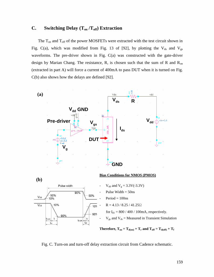
159
C. Switching Delay (Ton /Toff) Extraction
The Ton and Toff of the power MOSFETs were extracted with the test circuit shown in
Fig. C(a), which was modified from Fig. 13 of [92], by plotting the Vds and Vgs
waveforms. The pre-driver shown in Fig. C(a) was constructed with the gate-driver
design by Marian Chang. The resistance, R, is chosen such that the sum of R and Ron
(extracted in part A) will force a current of 400mA to pass DUT when it is turned on Fig.
C(b) also shows how the delays are defined [92].
Fig. C. Turn-on and turn-off delay extraction circuit from Cadence schematic.
Vdd
R
Ids
Vgs
Vds
Vg
GND
GND
Vdd
Bias Conditions for NMOS (PMOS)
- Vdd and Vg = 3.3V(-3.3V)
- Pulse Width = 50ns
- Period = 100ns
- R = 4.13 / 8.25 / 41.25Ω
for Id1 = 800 / 400 / 100mA, respectively.
- Vgs and Vds = Measured in Transient Simulation
Therefore, Ton = Td(on) + Tr and Toff = Td(off) + Tf
(a)
(b)
DUT
Pre-driver

160
APPENDIX-III: Process Flow of SJ-FINFET
Fabrication Steps on 4” N-type SOI Wafer
Step
No. Process Equipment Requirements
0 Alignment Mark
0.1 Sulfuric clean WET-A1: Standard Clean 120°C, 10min
0.2 HF dip WET-A2: HF:H20 (1:50) 1min
0.3 DI rinse / Spin dry DI rinse, Spin dry-1 and -2 4 cycles
0.4 Photoresist coating SVG Coater Track Program 1-4-7, P/R=1075
0.5 Pre-bake SUSS Hot Plate 90°C, 1min
0.6 Photoresist exposure ASML Stepper 5000 Energy: 350 (i-line)
0.7 Soft-bake SUSS Hot Plate 110°C, 1min
0.8 Photoresist develop SVG Developer Track Program 1-7
0.9 Hard-bake Imperial V 120°C, 10min
0.10 Descum IPC-4000 O2 Asher 2min
0.11 Inspection Optical microscope Check the mask pattern
0.12 Silicon plasma etch LAM 490 (Front) Etch = 120nm
0.13 Photoresist O2 ashing IPC-4000 O2 Asher 20min
0.14 Photoresist acid strip WET-E4: Resist Strip 120°C, 10min, P/R inspect
0.15 Inspection Alpha-Step Depth measurement
1 Active / Isolation
1.1 Sulfuric clean WET-A1: Standard Clean 120°C, 10min
1.2 HF dip WET-A2: HF:H20 (1:50) 1min
1.3 DI rinse / Spin dry DI rinse, Spin dry-1 and -2 4 cycles
1.4 Pad oxide growth D1: Dry Oxidation 300Å, 950°C
1.5 Nitride Deposition B2: CVD Furnace Nitride 2500 Å, 780°C
1.6 Photoresist coating SVG Coater Track Program 1-4-7, P/R=1075
1.7 Pre-bake SUSS Hot Plate 90°C, 1min
1.8 Mask #1: Active ASML Stepper 5000 Energy: 350 (i-line)
1.9 Soft-bake SUSS Hot Plate 110°C, 1min
1.10 Photoresist develop SVG Developer Track Program 1-7
1.11 Hard-bake Imperial V 120°C, 10min
1.12 Descum IPC-4000 O2 Asher 2min
1.13 Nitride Etch AME-8110 Etcher: P2 End-point detection
1.14 Inspection NanoSpec / Alpha-Step Step-thickness
1.15 Oxide Etch AME-8110 Etcher: P3 10% over-etch
1.16 Inspection NanoSpec / Alpha-Step Step-thickness
1.17 Deep-Si Etch DRY-ICP-Si S011, Etch = 3.6µm, 70 cycles
1.18 Inspection NanoSpec / Alpha-Step Step-thickness
1.19 Photoresist Ash IPC-4000 O2 Asher 20min
1.20 Photoresist acid strip WET-E4: Resist Strip 120°C, 10min, P/R inspect
1.21 Sulfuric clean WET-A1: Standard Clean 120°C, 10min
1.22 HF dip WET-A2: HF:H20 (1:50) 1min
1.23 DI rinse / Spin dry DI rinse, Spin dry-1 and -2 4 cycles
1.24 Liner Oxidation D1: Dry Oxidation 500 Å, 1000°C
1.25 Isolation Oxide Depo. B4: CVD Furnace LTO 4.5µm, 425°C, 115 Å /min,
O2:50 sccm SiH4: 40 sccm

161
Step
No. Process Equipment Requirements
1.26 DTI Densification D4: Annealing 900°C, 30min
1.27 CMP: Planarization CMP1: Strasbaugh 6EC 4.0µm removal
1.28 Post-CMP Cleaning CMP2: USI wafer washer DI wafer
1.29 LTO Dry-etch AME-8110 Etcher: P3 Etch: 4000 Å
1.30 LTO Wet-etch WET-A2: HF:H20 (1:50) Etch: 1000 Å , 16min
1.31 Nitride Removal WET-C1: Nitride Strip H3PO4 @ Temp=165°C,
Selectivity: Si3N4:LTO > 25
1.32 Pad Oxide Removal WET-A2: HF:H20 (1:50) 25°C, 5min
1.33 DI rinse / Spin dry DI rinse, Spin dry-1 and -2 4 cycles
2 PBODY: P-Body
2.1 Sulfuric clean WET-A1: Standard Clean 120°C, 10min
2.2 HF dip WET-A2: HF:H20 (1:50) 1min
2.3 DI rinse / Spin dry DI rinse, Spin dry-1 and -2 4 cycles
2.4 Sacrificial Oxidation D1: Dry Oxidation 250 Å, 850C, 10min, 950C,
35min
2.5 Nitride Deposition B2: CVD Furnace Nitride 4000 Å, 780C
2.6 Photoresist coating SVG Coater Track Program 1-4-7, P/R=1075
2.7 Pre-bake SUSS Hot Plate 90C, 1min
2.8 Mask #2: PBODY ASML Stepper 5000 Energy: 350 (i-line)
2.9 Soft-bake SUSS Hot Plate 110C, 1min
2.10 Photoresist develop SVG Developer Track Program 1-7
2.11 Hard-bake Imperial V 120°C, 10min
2.12 Descum IPC-4000 O2 Asher 2min
2.13 Nitride Etch AME-8110 Etcher: P2 End-point detection
2.14 Inspection NanoSpec / Alpha-Step Step-thickness
2.15 Oxide Etch AME-8110 Etcher: P3 10% over-etch
2.16 Inspection NanoSpec / Alpha-Step Step-thickness
2.17 Deep-Si Etch DRY-ICP-Si S011, Etch = 2.2um, 36 cycles
2.18 Inspection NanoSpec / Alpha-Step Step-thickness
2.19 Photoresist Ash IPC-4000 O2 Asher 20min
2.20 Photoresist acid strip WET-E4: Resist Strip 120°C, 10min, P/R inspect
2.21 Sulfuric clean WET-A1: Standard Clean 120°C, 10min
2.22 HF dip WET-A2: HF:H20 (1:50) 1min
2.23 DI rinse / Spin dry DI rinse, Spin dry-1 and -2 4 cycles
2.24 Inspection SEM: Cross-section Cross-section by test wafer #1.
2.25 Tilted Implant: 45deg. Varian CF3000 Species=Boron,
Energy(keV)=180,
Dose(/cm2)=2.2E14, Tilt=45deg
2.26 Nitride Removal WET-C1: Nitride Strip H3PO4 @ Temp=165°C,
Selectivity: Si3N4:LTO > 25
2.27 Pad Oxide Removal WET-A2: HF:H20 (1:50) 5min, 25C
2.28 DI rinse / Spin dry DI rinse, Spin dry-1 and -2 4 cycles
2.29 Trench Ox. Liner D1: Dry Oxidation 250A, 850C, 10min, 950C,
35min,
2.30 P-body diffusion D4: Annealing 950C, 10min, 1050C, 45min
2.30 LTO Gap-Filling B4: CVD Furnace LTO 3.0µm, 425°C, 115 Å/min,
O2:50 sccm SiH4: 40 sccm
2.31 LTO Densification D4: Annealing 850C, 10min, 900C, 30min
2.32 CMP: Planarization CMP1: Strasbaugh 6EC 2.5um LTO removal
2.33 Post-CMP Cleaning CMP2: USI wafer washer DI wafer
2.34 LTO Dry-etch AME-8110 Etcher: P3 Etch: 5000Å

162
Step
No. Process Equipment Requirements
2.35 LTO Wet-etch WET-A2: HF:H20 (1:50) Etch: 1000Å , 16min
3 SJ-drift
3.1 Sulfuric clean WET-A1: Standard Clean 120°C, 10min
3.2 HF dip WET-A2: HF:H20 (1:50) 1min
3.3 DI rinse / Spin dry DI rinse, Spin dry-1 and -2 4 cycles
3.4 Sacrificial Oxidation D1: Dry Oxidation 250Å, 850°C, 5min, 950°C,
35min, 850°C, 5min
3.5 Nitride Deposition B2: CVD Furnace Nitride 5000 Å, 780C, 8Hrs
3.6 Photoresist coating SVG Coater Track Program 1-4-7, P/R=1075
3.7 Pre-bake SUSS Hot Plate 90°C, 1min
3.8 Mask #3: IP ASML Stepper 5000 Energy: 320 (i-line)
3.9 Soft-bake SUSS Hot Plate 110°C, 1min
3.10 Photoresist develop SVG Developer Track Program 1-7
3.11 Hard-bake Imperial V 120°C, 10min
3.12 Descum IPC-4000 O2 Asher 2min
3.13 Nitride Etch AME-8110 Etcher: P2 End-point detection
3.14 Inspection NanoSpec / Alpha-Step Step-thickness
3.15 Oxide Etch AME-8110 Etcher: P3 10% over-etch
3.16 Inspection NanoSpec / Alpha-Step Step-thickness
3.17 Deep-Si Etch DRY-ICP-Si S011, Etch = 2.2µm, 36 cycles
3.18 Inspection NanoSpec / Alpha-Step Step-thickness
3.19 Photoresist Ash IPC-4000 O2 Asher 20min
3.20 Photoresist acid strip WET-E4: Resist Strip 120°C, 10min, P/R inspect
3.21 Sulfuric clean WET-A1: Standard Clean 120°C, 10min
3.22 HF dip WET-A2: HF:H20 (1:50) 1min
3.23 DI rinse / Spin dry DI rinse, Spin dry-1 and -2 4 cycles
3.24 Inspection SEM: Cross-section Cross-section by test wafer #2.
3.25 Tilted Implant: 2 x L/R
and 2 x T/B
Varian CF3000 Species=Boron,
Energy(keV)=80/45,
Dose(/cm2)=3.5E13/2,4,6,and
8E13, Tilt=45deg / 12deg
3.25A Trench Ox. Liner D1: Dry Oxidation 200Å, 850°C, 10min, 950°C,
20min,
3.26 LTO Gap-Filling B4: CVD Furnace LTO 3.0µm, 425°C, 115 Å/min,
O2:50 sccm SiH4: 40 sccm
3.27 LTO Densification D4: Annealing 850°C, 10min, 900°C, 20min
3.28 CMP: Planarization CMP1: Strasbaugh 6EC 2.5µm removal
3.29 Post-CMP Cleaning CMP2: USI wafer washer DI wafer
3.30 LTO Dry-etch AME-8110 Etcher: P3 Etch: 5000Å
3.31 LTO Wet-etch WET-A2: HF:H20 (1:50) Etch: 1000Å , 16min
3.32 Nitride Removal WET-C1: Nitride Strip H3PO4 @ Temp=165°C,
Selectivity: Si3N4:LTO > 25
3.33 Pad Oxide Removal WET-A2: HF:H20 (1:50) 25°C, 5min
3.34 DI rinse / Spin dry DI rinse, Spin dry-1 and -2 4 cycles
4 Trench Gate
4.1 Sulfuric clean WET-A1: Standard Clean 120°C, 10min
4.2 HF dip WET-A2: HF:H20 (1:50) 1min
4.3 DI rinse / Spin dry DI rinse, Spin dry-1 and -2 4 cycles
4.4 Photoresist coating SVG Coater Track Program 1-4-7, P/R=1075
4.5 Pre-bake SUSS Hot Plate 90°C, 1min

163
Step
No. Process Equipment Requirements
4.6 Mask #4: OD2 ASML Stepper 5000 Energy: 350 (i-line)
4.7 Soft-bake SUSS Hot Plate 110°C, 10min
4.8 Photoresist develop SVG Developer Track Program 1-7
4.9 Hard-bake Imperial V 120°C, 10min
4.10 Descum IPC-4000 O2 Asher 2min
4.11 Deep-Si Etch DRY-ICP-Si S011, Etch = 2µm, 36 cycles
4.12 Photoresist Ash IPC-4000 O2 Asher 20min
4.13 Photoresist acid strip WET-E4: Resist Strip 120°C, 10min, P/R inspect
4.14 Sulfuric clean WET-A1: Standard Clean 120°C, 10min
4.15 HF dip WET-A2: HF:H20 (1:50) 1min
4.16 DI rinse / Spin dry DI rinse, Spin dry-1 and -2 4 cycles
4.17 Inspection SEM: Cross-section Cross-section by test wafer #3.
4.18 Gate oxide growth D1: Dry Oxidation 300Å, 850°C, 10min, 950°C,
40min
4.19 Amorphous-Si
deposition (In-situ)
CVD Furnace A3 Poly 5000Å, 570°C
4.20 Gate Transformation to
Poly-Si
RTP-600S: Rapid Thermal 1000°C, 30sec, 900°C, 30min
4.21 Photoresist coating SVG Coater Track Program 111, P/R 204
4.22 Hard-bake Imperial V 120°C, 30min
4.23 Backside Poly-Si Etch LAM 490 Etch rate = 400nm/min, EPT by
Channel 12.
4.24 Backside Gox Etch WET-C3: BOE Etch 25°C, 1min
4.25 DI rinse / Spin dry DI rinse, Spin dry-1 and -2 4 cycles
4.26 Photoresist acid strip WET-E4: Resist Strip 120°C, 10min, P/R inspect
4.27 DI rinse / Spin dry DI rinse, Spin dry-1 and -2 4 cycles
5 Gate Poly
5.1 Photoresist coating SVG Coater Track Program 1-4-7, P/R=1075
5.2 Pre-bake SUSS Hot Plate 90°C, 10min
5.3 Mask #5: POLY1 ASML Stepper 5000 Energy: 350 (i-line)
5.4 Soft-bake SUSS Hot Plate 110°C, 10min
5.5 Photoresist develop SVG Developer Track Program 1-7
5.6 Hard-bake Imperial V 120°C, 10min
5.7 Descum IPC-4000 O2 Asher 2min
5.8 Poly-Si Etch DRY-ICP-Poly Etch = 5000Å, EPD
5.9 Photoresist Ash IPC-4000 O2 Asher 20min
5.10 Photoresist acid strip WET-E4: Resist Strip 120°C, 10min, P/R inspect
5.11 Sulfuric clean WET-A1: Standard Clean 120°C, 10min
5.12 HF dip WET-A2: HF:H20 (1:50) 1min
5.13 DI rinse / Spin dry DI rinse, Spin dry-1 and -2 4 cycles
5.14 Inspection NanoSpec / Alpha-Step Step-thickness
5.15 Inspection SEM: Cross-section Cross-section by test wafer #4.
6 N+ Source
6.1 Sacrificial Oxidation D1: Dry Oxidation 250Å, 850°C, 10min, 950°C,
35min
6.2 Nitride Deposition B2: CVD Furnace Nitride 4000Å, 780°C
6.3 Photoresist coating SVG Coater Track Program 147, P/R=1075
6.4 Pre-bake SUSS Hot Plate 90C, 1min
6.5 Mask #2: PBODY ASML Stepper 5000 Energy: 350 (i-line)
6.6 Soft-bake SUSS Hot Plate 110°C, 1min

164
Step
No. Process Equipment Requirements
6.7 Photoresist develop SVG Developer Track Program 17
6.8 Hard-bake Imperial V 120°C, 10min
6.9 Descum IPC-4000 O2 Asher 2min
6.10 Nitride Etch AME-8110 Etcher: P2 End-point detection
6.11 Inspection NanoSpec / Alpha-Step Step-thickness
6.12 Oxide Etch AME-8110 Etcher: P3 10% over-etch
6.13 Inspection NanoSpec / Alpha-Step Step-thickness
6.14 LTO Etch AME-8110 Etcher: P3 Etch = 1.8um
6.15 Inspection NanoSpec / Alpha-Step Measure the LTO thickness
6.16 Photoresist Ash IPC-4000 O2 Asher 20min
6.17 Photoresist acid strip WET-E4: Resist Strip 120°C, 10min, P/R inspect
6.18 Tilted Implant: 45deg. Varian CF3000 Species=Phosphorous,
Energy(keV)=180,
Dose(/cm2)=7E14, Tilt=45deg
6.19 Trench Ox. Liner D1: Dry Oxidation 200Å, 850°C, 10min, 950°C,
20min,
6.20 LTO Gap-Filling B4: CVD Furnace LTO 3.0µm, 425°C, 115 Å/min,
O2:50 sccm SiH4: 40 sccm
6.21 LTO Densification D4: Annealing 850°C, 10min, 900°C, 20min
6.22 CMP: Planarization CMP1: Strasbaugh 6EC 2.5µm removal
6.23 Post-CMP Cleaning CMP2: USI wafer washer DI wafer
6.24 LTO Dry-etch AME-8110 Etcher: P3 Etch: 4000Å
6.25 LTO Wet-etch WET-A2: HF:H20 (1:50) Etch: 1000Å , 16min
6.26 Sulfuric clean WET-A1: Standard Clean 120°C, 10min
6.27 HF dip WET-A2: HF:H20 (1:50) 1min
6.28 DI rinse / Spin dry DI rinse, Spin dry-1 and -2 4 cycles
7 N+ Drain
7.1 Photoresist coating SVG Coater Track Program 1-4-7, P/R=1075
7.2 Pre-bake SUSS Hot Plate 90°C, 1min
7.3 Mask #6: NIMP ASML Stepper 5000 Energy: 350 (i-line)
7.4 Soft-bake SUSS Hot Plate 110°C, 1min
7.5 Photoresist develop SVG Developer Track Program 1-7
7.6 Hard-bake Imperial V 120°C, 10min
7.7 Descum IPC-4000 O2 Asher 2min
7.8 Oxide Etch AME-8110 Etcher: P3 10% over-etch
7.9 Inspection NanoSpec / Alpha-Step Step-thickness
7.10 Deep-Si Etch DRY-ICP-Si S011, Etch = 2.1µm, 36 cycles
7.11 Inspection NanoSpec / Alpha-Step Step-thickness
7.12 Tilted Implant: -45deg. Varian CF3000 Species=Phosphorous/Arsenic,
Energy(keV)=180/200,
Dose(/cm2)=E, Tilt=45deg
7.13 Photoresist Ash IPC-4000 O2 Asher 20min
7.14 Photoresist acid strip WET-E4: Resist Strip 120°C, 10min, P/R inspect
7.15 Sulfuric clean WET-A1: Standard Clean 120°C, 10min
7.16 HF dip WET-A2: HF:H20 (1:50) 1min
7.17 DI rinse / Spin dry DI rinse, Spin dry-1 and -2 4 cycles
7.18 Trench Ox. Liner D1: Dry Oxidation 200Å, 850°C, 10min, 950°C,
20min,
7.19 LTO Gap-Filling B4: CVD Furnace LTO 4.0µm, 425°C, 115 Å/min,
O2:50 sccm SiH4: 40 sccm
7.20 LTO Densification D4: Annealing 850C, 10min, 900C, 20min

165
Step
No. Process Equipment Requirements
7.21 S/D Annealing RTP-600S: Rapid Thermal 1000°C, 15min
7.22 CMP: Planarization CMP1: Strasbaugh 6EC 1.0µm removal
7.23 Post-CMP Cleaning CMP2: USI wafer washer DI wafer
8 P+ Contact
8.1 Photoresist coating SVG Coater Track Program 1-4-7, P/R=1075
8.2 Pre-bake SUSS Hot Plate 90°C, 1min
8.3 Mask #7: PIMP ASML Stepper 5000 Energy: 350 (i-line)
8.4 Soft-bake SUSS Hot Plate 110°C, 1min
8.5 Photoresist develop SVG Developer Track Program 1-7
8.6 Hard-bake Imperial V 120°C, 10min
8.7 Descum IPC-4000 O2 Asher 2min
8.8 LTO Etch AME-8110 Etcher: P3 Etch = 2.8µm
8.9 Photoresist Ash IPC-4000 O2 Asher 20min
8.10 Photoresist acid strip WET-E4: Resist Strip 120°C, 10min, P/R inspect
8.11 Sulfuric clean WET-A1: Standard Clean 120°C, 10min
8.12 HF dip WET-A2: HF:H20 (1:50) 2min
8.13 DI rinse / Spin dry DI rinse, Spin dry-1 and -2 4 cycles
8.14 Inspection NanoSpec / Alpha-Step / SEM Step-thickness, Cross-section
8.14A HF dip (optional) WET-A2: HF:H20 (1:50) + 1min until no LTO
8.15 Ion Implant: default Varian CF3000 Species=Boron,
Energy(keV)=180,
Dose(/cm2)=E, Tilt=7deg
8.16 Trench Ox. Liner D1: Dry Oxidation 200Å, 850°C, 10min, 950°C,
20min,
8.17 LTO Gap-Filling B4: CVD Furnace LTO 4.0µm, 425°C, 115 Å/min,
O2:50 sccm SiH4: 40 sccm
8.18 LTO Densification D4: Annealing 900°C, 20min
8.19 CMP: Planarization CMP1: Strasbaugh 6EC 1.0µm removal
8.20 Post-CMP Cleaning CMP2: USI wafer washer DI wafer
9 Contact Openings
9.1 Photoresist coating SVG Coater Track Program 1-4-7, P/R=1075
9.2 Pre-bake SUSS Hot Plate 90°C, 1min
9.3 Mask #8: CONT ASML Stepper 5000 Energy: 350 (i-line)
9.4 Soft-bake SUSS Hot Plate 110°C, 1min
9.5 Photoresist develop SVG Developer Track Program 1-7
9.6 Hard-bake Imperial V 120°C, 10min
9.7 Descum IPC-4000 O2 Asher 2min
9.8 LTO Etch AME-8110 Etcher: P3 Etch = 3µm, 10% over-etch
9.9 Photoresist Ash IPC-4000 O2 Asher 20min
9.10 Photoresist acid strip WET-E4: Resist Strip 120°C, 10min, P/R inspect
9.11 Sulfuric clean WET-A1: Standard Clean 120°C, 10min
9.12 HF dip WET-A2: HF:H20 (1:50) 2min
9.13 DI rinse / Spin dry DI rinse, Spin dry-1 and -2 4 cycles
9.14 Inspection NanoSpec / Alpha-Step Step-thickness
9.14A HF dip (optional) WET-A2: HF:H20 (1:50) + 1min until no LTO
9.14B Inspection (optional) NanoSpec / Alpha-Step Step-thickness
10 Metallization
10.1 Al Sputter Deposition Varian 3180: Al:1wt%Si Thickness = 1µm,
Rate = 18.2nm/sec.

166
Step
No. Process Equipment Requirements
10.2 DI rinse / Spin dry DI rinse, Spin dry-1 and -2 4 cycles
10.3 Photoresist coating SVG Coater Track Program 1-4-7, P/R=1075
10.4 Pre-bake SUSS Hot Plate 90°C, 1min
10.5 Mask #9: M1 ASML Stepper 5000 Energy: 350 (i-line)
10.6 Soft-bake SUSS Hot Plate 110°C, 1min
10.7 Photoresist develop SVG Developer Track Program 1-7
10.8 Hard-bake Imperial V 120°C, 10min
10.9 Descum IPC-4000 O2 Asher 2min
10.10 Inspection SEM: Cross-section Cross-section by test wafer #5.
10.11 Al Etch AME-8130 Etch = 1µm, Rate = 150nm/min
10.12 Inspection NanoSpec / Alpha-Step Step and Oxide Thickness
10.13 DI rinse / Spin dry DI rinse, Spin dry-1 and -2 4 cycles
10.14 Photoresist Ash IPC-4000 O2 Asher 20min
10.15 Inspection Optical Microscope P/R removal inspect
10.16 DI rinse / Spin dry DI rinse, Spin dry-1 and -2 4 cycles
10.17 Forming Gas Anneal ASM C4: FGA Time=30min, Temp=400°C,
N2:H2=20:1
10.18 Electrical Test HP4156: Parameter Analyzer

167
List of Publication
Journal and Conference Papers
A. Yoo, J. C. W. Ng, J. K. O. Sin, and W. T. Ng, “Sub-100V Lateral SJ-FINFETs in
a 0.5µm CMOS-compatible Process,” IEEE Transactions on Electron Devices, Aug,
2010. (Submitted)
A. Yoo, J. C. W. Ng, J. K. O. Sin, and W. T. Ng, “High Performance CMOS-
compatible Superjunction FINFETs for Sub-100V Applications,” IEEE International
Electron Devices Meeting, Dec, 2010. (Accepted for oral presentation)
A. Yoo and W. T. Ng, “Sub-200V Lateral SJ-FINFETs with Low On-Resistance,”
IEEE 10th
International Seminar on Power Semiconductors, ISPS‟10, Prague, Czech
Republic, September 1-3, 2010. (Accepted for oral presentation)
A. Yoo, Y. Onishi, H. P. E. Xu, and W. T. Ng, “Low Voltage Lateral SJ-FINFETs
with Deep Trench p-Drift Region,” IEEE Electron Device Letters, vol. 30, no. 8, pp.
858-860, 2009.
A. Yoo, M. Chang, O. Trescases, and W. T. Ng, “Smart Power IC Design
Methodology Based on a New Figure of Merit (FOM) for Standard CMOS
Technology,” IEEE 8th
International Seminar on Power Semiconductors, ISPS‟08,
Prague, Czech Republic, Aug 27-29, 2008.
A. Yoo, M. Chang, O. Trescases, and W. T. Ng, “High Performance Low-Voltage
Power MOSFETs with Hybrid Waffle Layout Structure in a 0.25µm Standard CMOS
Process,” IEEE 20th
International Symposium on Power Semiconductors and IC‟s,
ISPSD‟08 Proceedings, pg.95-98, Orlando, Florida, USA, May 18-22, 2008.
A. Yoo, M. Chang, O. Trescases, H. Wang, and W.T. Ng, “FOM (Figure of Merit)
Analysis of Low Voltage Power MOSFETs in DC-DC Converter,” IEEE Electron
Devices and Solid-State Circuits, pg.1039-1042, Tainan, Taiwan, 2007.
W. T. Ng and A. Yoo, “Advanced Lateral Power MOSFETs for Power Integrated
Circuits,” Solid-State and Integrated Circuit Technology, ICSICT‟10, Shanghai,
China, Nov 1-4, 2010. (Submitted)
H. Wang, A. Yoo, H. P. E. Xu, and W.T. Ng, “A Floating RESURF EDMOS with
enhanced Ruggedness and Safe operating Area,” IEEE Internal Conference on
Electron Devices and Solid-State Circuits, Taiwan, 2007.
H. Wang, A. Yoo, H. P. E. Xu, and W.T. Ng, “A Floating RESURF EDMOS with
enhanced Safe Operating Area,” International Workshop on the Physics of
Semiconductor Devices, India, 2007.
W. T. Ng, M. Chang, A. Yoo, J. Langer, T. Hedquist, and H. Schweiss, “High Speed
CMOS Output Stage for Integrated DC-DC Converters,” Solid-State and Integrated
Circuit Technology, ICSICT‟08, Beijing, China, 2008.
Patents
A. Yoo, H.S. Kang, and H.J. Shin, “Shared Contact Structure Having Corner
Protection Pattern, Semiconductor Devices, and Methods of Fabricating the Same,”
US Patent Application No. US11/377,455, March 17, 2006.