design and implementation of carry select adder without ...206-209).pdf · it discuss about the...
TRANSCRIPT

ICETET 2014 | DS0EC033 P a g e | 206
Design and Implementation of Carry Select Adder without using Multiplexer
P.Mahipal Reddy1, S.Kumaraswamy2 and B.Dharma3
1 2 3 Department of Electronics & Communication Engineering, 1 2 3 Sree Chaitanya College o Engineering, Karimnagar, Telangana, India – 505 481
1: [email protected] , 2 [email protected] and 3 [email protected]
ABSTRACT
Design of high performance digital adder with reduced area and low power consumption is an important
requirement in advanced digital processors for faster computation. In digital adder circuits, the speed of
addition is limited by the time required for a carry to propagate through the adder. Many different approaches
had already been suggested to improve the performance of the adder. Carry Select Adder is one among them
and is used to solve the problem of carry propagation delay by independently generating multiple carries and
then select a carry to generate the final sum. The speed of operation of such an adder is limited by carry
propagation from input to output. Our work is based on designing an optimized adder for advanced
processors. It discuss about the implementation of Carry Select Adder without using Multiplexer for final
selection. Parallel adder configuration is also used to reduce the delay between stages. Removing the MUX
stage will reduce the area as well as propagation delay to give much higher performance for the adder. The
Kogge Stone parallel approach will generate fast carry for intermediate stages.
Keywords: CSA, MUX.
I. INTRODUCTION
This approach will reduce the problem of existing
scheme and CSA [2] is one among them which will
reduce the carry propagation delay problem. In CSA,
requirement of producing two adders and final
selection multiplexers make it consuming more area,
even though carry propagation delay is reduced
much. Buffering inverters are to be added
appropriately to support these large loads and there
is a corresponding increase in the delay. Brent &
Kung [3] proposed the fan-out trees such that the
lateral fan-out of each node is restricted to unity, as
for the Kogge Stone graph, but without the explosion
of wires.
Although looks attractive it increases the logical
depth. This illustrates the approach of carry select
adder implementation to achieve minimum delay
and reduced area without increasing the fan-out.
II. RIPPLE CARRY ADDER
There are many carry select adder approaches
available but most of them use ripple carry adders
[1] to implement the adder.
Disadvantages of existing system
Delay is more.
It requires more area.
Power consumption is more
In electronics, an adder or summer is a digital circuit
that performs addition of numbers. In many
computers and other kinds of processors, adders are
used not only in the arithmetic logic unit(s), but also
in other parts of the processor, where they are used
to calculate, table indices, addresses and similar
operations.
Although adders can be constructed for many
numerical representations, such as binary-coded
decimal or excess-3 the most widely recognized
adders work on binary numbers. In cases where
two's complement or ones' complement is being
used to represent negative numbers, it is trivial to
modify an adder into an added. Other signed
number representations require a more complex
adder.
The adder we are using here is a ripple carry adder.
It is possible to create a logical circuit using multiple
full adders to add N-bit numbers. Each full adder
Proceedings of International Conference on Emerging Trends in
Electronics & Telecommunications (ICETET) 13th - 14th December -2014
Karimnagar, Telangana, India (DS0EC033)
ISSN (online): 2349-0020
ISSN (print): 2394-4544

Proceedings of International Conference on Emerging Trends in Electronics & Telecommunications (ICETET-14)
13th - 14th December -2014, Karimnagar, Telangana, India; ISSN (online): 2349-0020, ISSN (print): 2394-4544
ICETET 2014 | DS0EC033 P a g e | 207
inputs a Cin, which is the Cout of the previous adder.
This kind of adder is called a ripple-carry adder [5],
since each carry bit "ripples" to the next full adder.
Note that the first (and only the first) full adder may
be replaced by a half adder.
The ripple carry adder is implemented using full
adder as the basic building block.
Fig.1. 4 Bit Ripple Carry Adders
The Fig.1 shows 4 bit ripple carry adder which is
constructed with using 4 full adders. The input carry
in the least significant position is 0. Each full adder
receives the corresponding bits of A and B and the
input carry and generate the sum bit for S and the
output carry. The output carry in each position is the
input carry of the next-higher-order position.
It can be inferred, that for N bit addition, the
proposed ripple carry adder architecture uses only
N reversible gates and produces only 3N garbage
outputs. But, the ripple carry adder [4] using our
proposed gate (PG) is the most optimized one.
III. PROPOSED SYSTEM
To generate the fast carry for intermediate stages by
using kogge-stone adder. The carry propagation
delay of adder is proportional to log2 (n) and the
number of logic elements used is proportional to
nlog2 (n), where n is the number of bits used in
addition. In this the carry select adder is
implemented It mainly focus on to improve the
performance of adder with reduced area, high speed
and low power consumption. In digital adder
circuits, the speed of addition is limited by the time
required for a carry to propagate through the adder.
Carry Select Adder (CSA)[6] is one among them and
is used to solve the problem of carry propagation
delay by independently generating multiple carries
and then select a carry to generate the final sum.
IV. DESIGN AND IMPLEMENTATION
Kogge-Stone (KS) adder is a parallel prefix form
Look ahead Adder [2]. Kogge-Stone adder can be
represented as a parallel prefix graph consisting of
carry operator nodes. The time required to generate
carry signals in this prefix adder is proportional to
log n. It is the fastest adder with focus on design
time and is the common choice for high performance
adders in industry.The better performance of Kogge-
Stone adder is because of its minimum logic depth
and bounded fan-out. On the other side it occupies
large silicon area.
The carry equations of KS adder are shown below.
The carry propagation delay of the adder is
proportional to log2 (n) and the number of logic
elements used is proportional to nlog2 (n), where n
is the number of bits used in addition. The carry for
different stages are
incpgc .001 (1)
incppgpgc 010.112 )( (2)
1121223 )( cppgpgc (3)
incpppp
gpgppgpgc
0123
011232334 )()(
(4)
11234
122343445 )()(
cpppp
gpgppgpgc
(5)
22345
233454556 )()(
cpppp
gpgppgpgc
(6)
33456
344565667 )()(
cpppp
gpgppgpgc
(7)
incpppppppp
pggppgpg
ppppgpgppgpgc
01234567
10123233
4567455676778
)]}()[(
{)()(
(8)
Fig. 2. 4 Bit Kogge Stone Adder.

Proceedings of International Conference on Emerging Trends in Electronics & Telecommunications (ICETET-14)
13th - 14th December -2014, Karimnagar, Telangana, India; ISSN (online): 2349-0020, ISSN (print): 2394-4544
ICETET 2014 | DS0EC033 P a g e | 208
Fig. 2 shows the 4 bit implementation of KS adder.
Implementation uses 31 two input logic elements
and has 8 units delay. For delay calculation XOR is
considered to have two units delay and all the other
elements have single unit delay.
Carry input for the intermediate stages can be
realized using Kogge Stone approach and by doing
so we can eliminate the carry propagation through
multiplexers as in CSA. CSA has lesser area
utilization compared to KS adder. Area utilization of
CSA can still be reduced by realizing the Cin=1 adder
from Cin=0 adder, instead of going for a separate
adder. Two different such realizations are discussed
in the next section.
V. KOGGE STONE CARRY SELECT ADDER
Fig. 3 shows the proposed method of
implementation of CSA. Here instead of using
simple Excess ladder, first zero finding logic is used.
Fig.3. Carry Select Adder with KS adder (c in =0).
If Cin =0, logic will select the KS Adder output as the
final output from LSB to MSB until it finds the first
occurrence of a zero. The proposed adder uses lesser
logic elements compared to CSA with MUX.
A) KS Adder The below analysis is the result of the
KS ADDER in Fig.4 which the inputs area, b and Cin.
The output is s and Cout. The input is taken as a=1111
and b=0101 and the output we get is s= 0100 and
carry out Cout =1.
Fig. 4. KS Adder.
B) SA with 16 bit KS adder
Fig. 5. CSA with 16 bit KS Adder.
The above analysis is the result of the 4bit with KS
CSA adder in which the inputs are ‘a’,‘b’ and Cin
and the output is ‘s’ and carry out is Cout . The input
is taken as a=Fh’4 and b=6h’4 and the output we get
is s=5h’4 and the carry out Cout=1.
The above analysis is the result of the 16bit KS CSA
adder in Fig.5 which the inputs are ‘a’ and ‘b’ and
the output is Sout and carry out is Cout. The input is
taken as a=FFFF h’4 and b=0000 h’4 and the output
we get is s=FFFF h’4 and the carry out Cout=0.
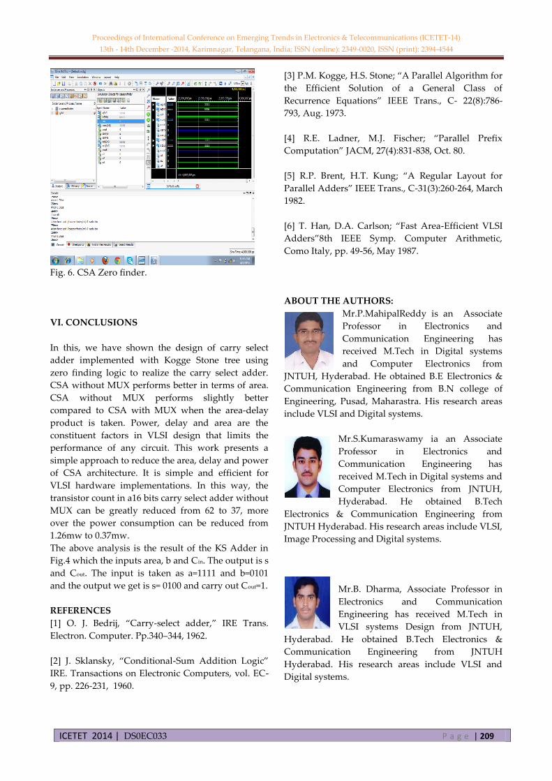
ii) CSA Zero finder From Fig.6 the input is taken as
a=1111 and b=0000 and the output we get is S=0000
and the carry out Cout.
Proceedings of International Conference on Emerging Trends in Electronics & Telecommunications (ICETET-14)
13th - 14th December -2014, Karimnagar, Telangana, India; ISSN (online): 2349-0020, ISSN (print): 2394-4544
ICETET 2014 | DS0EC033 P a g e | 209
Fig. 6. CSA Zero finder.
VI. CONCLUSIONS
In this, we have shown the design of carry select
adder implemented with Kogge Stone tree using
zero finding logic to realize the carry select adder.
CSA without MUX performs better in terms of area.
CSA without MUX performs slightly better
compared to CSA with MUX when the area-delay
product is taken. Power, delay and area are the
constituent factors in VLSI design that limits the
performance of any circuit. This work presents a
simple approach to reduce the area, delay and power
of CSA architecture. It is simple and efficient for
VLSI hardware implementations. In this way, the
transistor count in a16 bits carry select adder without
MUX can be greatly reduced from 62 to 37, more
over the power consumption can be reduced from
1.26mw to 0.37mw.
The above analysis is the result of the KS Adder in
Fig.4 which the inputs area, b and Cin. The output is s
and Cout. The input is taken as a=1111 and b=0101
and the output we get is s= 0100 and carry out Cout=1.
REFERENCES
[1] O. J. Bedrij, ‚Carry-select adder,‛ IRE Trans.
Electron. Computer. Pp.340–344, 1962.
[2] J. Sklansky, ‚Conditional-Sum Addition Logic‛
IRE. Transactions on Electronic Computers, vol. EC-
9, pp. 226-231, 1960.
[3] P.M. Kogge, H.S. Stone; ‚A Parallel Algorithm for
the Efficient Solution of a General Class of
Recurrence Equations‛ IEEE Trans., C- 22(8):786-
793, Aug. 1973.
[4] R.E. Ladner, M.J. Fischer; ‚Parallel Prefix
Computation‛ JACM, 27(4):831-838, Oct. 80.
[5] R.P. Brent, H.T. Kung; ‚A Regular Layout for
Parallel Adders‛ IEEE Trans., C-31(3):260-264, March
1982.
[6] T. Han, D.A. Carlson; ‚Fast Area-Efficient VLSI
Adders‛8th IEEE Symp. Computer Arithmetic,
Como Italy, pp. 49-56, May 1987.
ABOUT THE AUTHORS:
Mr.P.MahipalReddy is an Associate
Professor in Electronics and
Communication Engineering has
received M.Tech in Digital systems
and Computer Electronics from
JNTUH, Hyderabad. He obtained B.E Electronics &
Communication Engineering from B.N college of
Engineering, Pusad, Maharastra. His research areas
include VLSI and Digital systems.
Mr.S.Kumaraswamy ia an Associate
Professor in Electronics and
Communication Engineering has
received M.Tech in Digital systems and
Computer Electronics from JNTUH,
Hyderabad. He obtained B.Tech
Electronics & Communication Engineering from
JNTUH Hyderabad. His research areas include VLSI,
Image Processing and Digital systems.
Mr.B. Dharma, Associate Professor in
Electronics and Communication
Engineering has received M.Tech in
VLSI systems Design from JNTUH,
Hyderabad. He obtained B.Tech Electronics &
Communication Engineering from JNTUH
Hyderabad. His research areas include VLSI and
Digital systems.