design and construction of a voltage source converter for
TRANSCRIPT

TVE-MFE; 19001
Examensarbete 30 hpMaj 2019
Design and construction of a voltage source converter for a laboratory setup
Henrik Lindblom
Masterprogram i förnybar elgenereringMaster Programme in Renewable Electricity Production

Teknisk- naturvetenskaplig fakultet UTH-enheten Besöksadress: Ångströmlaboratoriet Lägerhyddsvägen 1 Hus 4, Plan 0 Postadress: Box 536 751 21 Uppsala Telefon: 018 – 471 30 03 Telefax: 018 – 471 30 00 Hemsida: http://www.teknat.uu.se/student
Abstract
Design and construction of a voltage source converterfor a laboratory setup
Henrik Lindblom
The grid stability and reliability is facing new challenges as the emerging number of intermittent renewable sources connected to the grid is increasing. With the introduction of the insulated-gate bipolar transistor, the three-phase VSC has grown more popular and is used in many applications.
In this thesis a two-Level Voltage Source Converter was designed and constructed with rated IGBT modules at 1200V and 150A. It focuses on the design, construction and control of said converter. The control is done through the LabVIEW FPGA module. Tests showed that the converter is working according to wanted specifications and can be used in a laboratory setup.
TVE-MFE; 19001Examinator: Irina TemizÄmnesgranskare: Mikael BergkvistHandledare: Markus Gabrysch

Contents
1 Introduction 11.1 Background . . . . . . . . . . . . . . . . . . . . . . . . . . . . . . . . . . . . . . . . 11.2 Objectives . . . . . . . . . . . . . . . . . . . . . . . . . . . . . . . . . . . . . . . . . 11.3 Limitations . . . . . . . . . . . . . . . . . . . . . . . . . . . . . . . . . . . . . . . . 21.4 Report structure . . . . . . . . . . . . . . . . . . . . . . . . . . . . . . . . . . . . . 2
2 Theory 32.1 Voltage source converter . . . . . . . . . . . . . . . . . . . . . . . . . . . . . . . . . 32.2 Space vectors and reference frame . . . . . . . . . . . . . . . . . . . . . . . . . . . . 5
2.2.1 Clarke transform . . . . . . . . . . . . . . . . . . . . . . . . . . . . . . . . . 62.2.2 Park transform . . . . . . . . . . . . . . . . . . . . . . . . . . . . . . . . . . 6
2.3 Phase-locked loop . . . . . . . . . . . . . . . . . . . . . . . . . . . . . . . . . . . . . 72.4 dq-current control . . . . . . . . . . . . . . . . . . . . . . . . . . . . . . . . . . . . 8
2.4.1 DC voltage control . . . . . . . . . . . . . . . . . . . . . . . . . . . . . . . . 92.5 Bipolar SPWM . . . . . . . . . . . . . . . . . . . . . . . . . . . . . . . . . . . . . . 9
3 Design of bidirectional converter 113.1 IGBT module . . . . . . . . . . . . . . . . . . . . . . . . . . . . . . . . . . . . . . . 113.2 Gate driver - 2SC0108T driver core . . . . . . . . . . . . . . . . . . . . . . . . . . . 12
3.2.1 Primary side . . . . . . . . . . . . . . . . . . . . . . . . . . . . . . . . . . . 123.2.2 Half bridge mode . . . . . . . . . . . . . . . . . . . . . . . . . . . . . . . . . 143.2.3 Secondary side . . . . . . . . . . . . . . . . . . . . . . . . . . . . . . . . . . 153.2.4 Active clamping . . . . . . . . . . . . . . . . . . . . . . . . . . . . . . . . . 17
3.3 DC capacitor . . . . . . . . . . . . . . . . . . . . . . . . . . . . . . . . . . . . . . . 17
4 LabView implementation 194.1 Measurements . . . . . . . . . . . . . . . . . . . . . . . . . . . . . . . . . . . . . . . 194.2 Bipolar SPWM . . . . . . . . . . . . . . . . . . . . . . . . . . . . . . . . . . . . . . 214.3 PLL . . . . . . . . . . . . . . . . . . . . . . . . . . . . . . . . . . . . . . . . . . . . 224.4 abc to dq transform . . . . . . . . . . . . . . . . . . . . . . . . . . . . . . . . . . . . 224.5 Current control . . . . . . . . . . . . . . . . . . . . . . . . . . . . . . . . . . . . . . 23
4.5.1 id and iq current control . . . . . . . . . . . . . . . . . . . . . . . . . . . . . 234.5.2 DC voltage control . . . . . . . . . . . . . . . . . . . . . . . . . . . . . . . . 24
4.6 dq to abc transform . . . . . . . . . . . . . . . . . . . . . . . . . . . . . . . . . . . . 254.7 Converter safety . . . . . . . . . . . . . . . . . . . . . . . . . . . . . . . . . . . . . 274.8 Real Time . . . . . . . . . . . . . . . . . . . . . . . . . . . . . . . . . . . . . . . . . 27
5 Results 295.1 Setup . . . . . . . . . . . . . . . . . . . . . . . . . . . . . . . . . . . . . . . . . . . 295.2 id and iq current control test . . . . . . . . . . . . . . . . . . . . . . . . . . . . . . 305.3 DC voltage control test . . . . . . . . . . . . . . . . . . . . . . . . . . . . . . . . . 32
6 Conclusions and future work 35
Bibliography 35
Appendix A Low voltage side schematic 38
Appendix B High voltage side schematic 39

Chapter 1
Introduction
1.1 Background
The grid stability and reliability is facing new challenges as the emerging number of grid-connectedintermittent renewable sources to the grid increases. Renewable resources often have an intermit-tent nature that can affect voltage and frequency fluctuation that varies with weather condition.Thus, the electric grid cannot rely only on renewable resources unless there is a huge capacityof electric storage or fast-response dispatchable sources such as hydro power with a dam or gasturbine.
Power electronics such as the Insulated gate bipolar junction transistor IGBT is considered to beone of the key technologies when introducing renewable energy sources. Converters built on this iswhat allows for efficient integration of renewable energy sources into the grid. They are the core forvoltage-source-converter-high-voltage direct current (VSC-HVDC) transmission technology and itovercomes the limitations of long distance AC transmission [1].
The VSC is inherently bi-directional in its power flow, meaning that the transmission permits activeand reactive power flow in either direction. It can be controlled to generate or absorb reactivepower independently of the active power flow. There are several applications where the VSC-HVDC transmission technology can be utilized such as, supply of power to isolated areas withoutgenerating resources, interconnection of two or more asynchronous AC networks and linking remoteoffshore wind-power plants to the mainland networks [2].
1.2 Objectives
A three-phase bi-directional AC-DC converter will be designed and constructed with rated IGBTmodules at 1200V and 150A. The constructed converter will be tested and its control will beimplemented in LabVIEW’s FPGA enviroment using a compactRIO. The aim is to build a studentlaboratory test setup with said converter, this includes
• Literature survey. The literature survey includes a general description of HVDC technology.
• Construction and testing of the converter. Once built, the converter will be tested both inrectification mode and in inverter mode.
• Control of the converter. The converter is controlled by a CompactRIO which is setup in theLabVIEW FPGA environment.
1

Uppsala University 2018 CHAPTER 1
1.3 Limitations
This master thesis focuses on the design, construction and control of a three-phase bi-directionalAC-DC converter. The technical aspect of connecting this to the grid is discussed and the theoryrevolves around it. However in this thesis the converter will not be connected to the grid but onlytested with a resistive load both for rectifying mode and inverting mode.
The converter control will be used in student laboratories and in the future it will be connectedwith another converter to form a HVDC-link. This thesis lays the ground for this implementationwith the control programming being able to control two converters at the same time.
1.4 Report structure
The report begins with an introduction to the HVDC converter and the objectives that guided thismasters thesis, followed by a more in depth description of the theory behind the voltage sourceconverter and its control.
The following chapters will describe the construction and design of the converter and the controlwhich is set up in the LabVIEW FPGA environment. Finally the results, finding and reflectionswill be presented.
2

Chapter 2
Theory
This chapter gives an introduction to the voltage source converter and covers the mathematicalmodel of the converter, reference frame transformation and control in the dq-reference frame.
2.1 Voltage source converter
Today there exist a wide variety of voltage source converters (VSC). With the introduction ofthe insulated-gate bipolar transistor (IGBT) the three-phase VSC has grown more popular and istoday used in many applications.
Diode clamped (NPC), flying capacitors (FCs) and cascaded H-bridge (CHB) are types of three-phase VSC converters to name a few. All these are multi-level converters and are derived from the2-level converter which is shown in figure 2.1 and is the one used in this thesis [3].
/2VDC
− /2VDC
VDC
2
VDC
2
0
vta
vtb
vtc
ia
ib
ia
Figure 2.1: Schematic of an ideal two-level VSC.
It is called 2-level since the AC sides of the converter can assume two voltage levels, VDCand −VDC . The converter can supply a bidirectional power flow between the DC-side and thethree-phase AC system [4].
The converter is controlled with pulse width modulation (PWM) as switching strategy. Fromthis and [4] p. 120 it can be derived that the AC-side terminal voltages of the ideal converter is.
3

Uppsala University 2018 CHAPTER 2
Vta = ma(t)VDC
2
Vtb = mb(t)VDC
2
Vtc = mc(t)VDC
2
(2.1)
where m(t) is a three-phase balanced modulation signal. With this it is possible to controlactive and reactive power flow of the converter. This will be further explained in chapter 2.4.
Figure 2.2 shows the VSC converter connected to the grid and a DC source. It also showsthe current controlled real/reactive power controller. The control is preformed in the dq-frame.With this configuration the converter can regulate the power flow with simple PI controllers ascompensators.
Seven measurements are needed for the control, phase voltages, phase currents and the DCvoltage. It is also good to monitor the DC current. These are then transformed into the dq-frameand fed into the compensators which either regulates the currents id and iq or VDC to a referencevalue. The compensator then returns the modulation signals in dq-frame. The chosen PWMstrategy takes the signals and output the switching pulses for the IGBTs.
θabc
dqPLL
PWM
θabc
dq
R L
R L
R Lva
vb
vc
vd vq id iq
VDC
mqmd
ia
ib
ic
iDC
Compensators in dq − f rame
CDC
VDCVDC,ref
id,ref iq,ref
vtb
vta
vtc
Figure 2.2: Schematic diagram of a current-controlled real-/reactive-power controller in dq-frame.
If the AC system is assumed to be ideal with a balanced sinusoidal three-phase source whichhas a constant frequency, the dynamics from of figure 2.2 can be described by
Ldiadt
= vta − va −Ria
Ldibdt
= vtb − vb −Rib
Ldicdt
= vtc − vc −Ric
(2.2)
depending on the control strategy, the VSC can be used as either a real-/reactive power con-troller or a DC voltage controller [4].
4

Uppsala University 2018 CHAPTER 2
2.2 Space vectors and reference frame
When controlling a three-phase VSC system some sort of closed loop compensator needs to beimplemented in order to obtain a wanted power flow. If it is desired to control a current i(t) ati(t)ref that is connected to a three-phase system, it means that it is a sinusoidal signal that needsto be tracked. In that case the steady-state value varies with time.
The compensator structure for sinusoidal command tracker is far more complex than a DCcommand tracker which has a time-invariant steady state value [4]. Therefore, the sinusoidalsignals of a balanced three phase system is converted to a DC-valued signal the control design canbe simplified. A balanced three-phase sinusoidal system can be expressed as
va(t) = V cos(ωt+ θ0)
vb(t) = V cos(ωt+ θ0 −2π
3)
vc(t) = V cos(ωt+ θ0 −4π
3)
(2.3)
If the quantities are voltages then va,b,c are phase voltages and V are the peak values. θ0 is theinitial phase angle. The phases time-response can be seen in figure 2.3 A. This system can in turnbe described by a space vector which is a complex function of time. In polar form it is given by
~v(t) =2
3(va(t) + ej
2π3 vb(t) + ej
4π3 vc(t)) (2.4)
This vector is presented in figure 2.4. The zero-sequence component can normally be disregardedand therefore it is possible to reduce the three-phase system to a equivalent two-phase system thathas a 90 phase-shift [1]. This transformation is called the Clarke transformation [5]. It is alsoknown as the αβ-frame. If the αβ-frame is then rotated around an angle θ a DC-valued signal isobtained as seen in figure 2.3 C. This transformation is called the park transformation [6] and itsimplifies the analysis and control of the system.
0 0.01 0.02 0.03 0.04
Time [S]
-1
-0.8
-0.6
-0.4
-0.2
0
0.2
0.4
0.6
0.8
1
0 0.01 0.02 0.03 0.04
Time [S]
-1
-0.8
-0.6
-0.4
-0.2
0
0.2
0.4
0.6
0.8
1
0 0.01 0.02 0.03 0.04
Time [S]
0
0.2
0.4
0.6
0.8
1
A B C
Figure 2.3: Time response for A) abc reference frame. B) αβ reference frame. C) dq reference frame.
5

Uppsala University 2018 CHAPTER 2
Figure 2.4: Space vector in the abc-, αβ- and dq-frame.
2.2.1 Clarke transform
The space vector from equation 2.4 can be rewritten and be given by its real and complex values
~v(t) = vα + jvβ (2.5)
Where vα and vβ are components of the α and β axis as seen in figure 2.4. This transformationcan be written in matrix form as
vαvβv0
=2
3
1 − 1
3 − 13
0√
32 −
√3
2
12
12
12
vavbvc
(2.6)
In a balanced system where va + cb + vc = 0 and thus v0 = 0. This transformation preserves theamplitudes of the variables. If a scaling constant K is introduced it is possible to get rms-value
scaling and power-invariant scaling by selecting K = 1√2
and K =√
23 , respectively [1].
The abc-frame can also be represented in terms of αβ. The inverse transform is given by
vavbvc
=
1 0 1
− 12
√3
2 1
− 12 −
√3
2 1
vαvβv0
(2.7)
2.2.2 Park transform
The signals are reduced from two to three when applying the Clarke transform but they are stillin general a sinusoidal function of time. If the Park transform is applied then the signals assumea DC-value whilst in a steady state. It is achieved by rotating the αβ- reference frame around anangle. This is known as the dq-transform and it is given by
vd + jvq = (vα + vβ)e−jθ(t) (2.8)
Where θ is the phase angle of the grid voltages and is defined as θ(t) = θ0 + ωt. By doing thisvd and vq are not time-varying and from figure 2.4 the following matrix relations can be obtained
6

Uppsala University 2018 CHAPTER 2
vdvqv0
=
cos(θ(t)) sin(θ(t)) 0
−sin(θ(t)) cos(θ(t)) 1
0 0 1
vαvβv0
(2.9)
The inverse transform is obtained when rotation of the dq-frame is canceled out. This is done bymultiplying both sides with ejθ(t) and thus changing to rotation direction to clockwise
vα + jvβ = (vd + vq)ejθ(t) (2.10)
The matrix relations can then be written asvαvβv0
=
cos(θ(t)) −sin(θ(t)) 0
sin(θ(t)) cos(θ(t)) 0
0 0 1
vdvqv0
(2.11)
In time domain a balanced three phase systems total instantaneous power can be described byP (t) = va(t)ia(t) + vb(t)ib(t) + vc(t)ic(t) and in [4] the instantaneous complex power is derived tobe
S(t) = P (t) + jQ(t) =3
2~v(t)~i∗(t) (2.12)
Where * denotes the complex conjugate. From 2.10 we get that ~v = (vd + vq)ejθ(t) and ~i∗ =
(id + iq)e−jθ(t) The instantaneous complex is then represented in the dq-frame and is formulated
as
P =3
2[vdid + vqiq]
Q =3
2[−vdiq + vqid]
(2.13)
It can be observed that if vq = 0 the real and reactive power are proportional to id and iq,respectively. This allows for full control of the power flow and is very usable in a three phase VSCsystem.
2.3 Phase-locked loop
The phase-locked loop, PLL transforms vabc to vdq and dynamically adjusts the rotational speedof the dq-frame to keep vq = 0 [4]. The space vector from 2.4 can be written as
~v(t) = V ej(ω+tθ0) (2.14)
from 2.14 and 2.8 we get
vd = V cos(ωt+ θ0 − θ(t))
vq = V sin(ωt+ θ0 − θ(t))(2.15)
By choosing θ(t) = ωt+ θ0 the desired result of keeping vq = 0 is obtained. There are severaldifferent PLL methods available, but synchronous reference frame phase-locked loop, SRF-PLL isthe standard configuration in three phase PLL applications [7]. This was also the one used in thisproject. Figure 2.5 shows the block diagram of the SRF-PLL.
α
β
a
b
c
α
β
d
q
vd
vqPI
ω
θ
va
vb
vc
vα
vβ ∫ωgΔωg
Figure 2.5: Block diagram for SRF-PLL.
7

Uppsala University 2018 CHAPTER 2
The input signal vq is fed into the PI controller which outputs the angular frequency deviation∆ω. ω = 2πf is then added to this which is finally integrated into θ. As it can be observed infigure 2.5 and in [1] page 194. θ can be formulated by.
θ =
∫ωgdt = ωt+
∫∆ωgdt (2.16)
2.4 dq-current control
The dq-frame control is based on 2.2. With the help from the selection of θ(t) = ωt + θ0 and thespace vector along with [4] p. 208 the equations can be deduced to
Ldiddt
= Lωiq −Rid + vtd − vd
Ldiqdt
= −Lωid −Riq + vtq − vq
(2.17)
Where vtd and vtq are equation 2.1 in dq-reference frame. Due to the presence of Lω thedynamics of id and iq are coupled [4] p 219. To decouple the dynamics we can write
md =2
VDC(ud − Lωiq + vd)
mq =2
VDC(uq + Lωid + vq)
(2.18)
Two new terms are introduced, ud and uq these are two new control inputs. Figure 2.6 showsthe block diagram implementation of equation 2.18. From 2.17, 2.1 in dq-frame and 2.18 thefollowing can be deduced
Ldiddt
= −Rid + ud
Ldiddt
= −Riq + uq
(2.19)
These equation describes two first-order, linear systems. Based on them id and iq can becontrolled by ud and uq which can be outputs from a simple PI compensator. In short, they canbe dimensioned by [4] p.221
kp = L/τi
ki = R/τi(2.20)
Where the time constant τi is a design choice.
PI
ωL
id
PI
ωL
iq
iq,ref
id,ref
VDC
2
md
mq
vd
vq
ud
uq
Figure 2.6: Block diagram for dq control. Based on equation 2.18.
8

Uppsala University 2018 CHAPTER 2
2.4.1 DC voltage control
Alternatively to controlling id and iq it is also possible to regulate the DC voltage via the currents.Due to the nonlinear characteristics of the model it is chosen to regulate V 2
DC instead of VDC .Practically this means that the energy is controlled instead voltage. When no control is active onthe converter it acts as an passive rectifier. By applying control it is possible to boost the DCvoltage. Following [8] p. 90 and [9] the following system model can be described as
1
2CdV 2
DC
dt=
3
2vdid − Pload (2.21)
And it turns out from [9] that the transfer function from id to W = V 2DC is
G(s) =W
id=
3vdsC
(2.22)
From this it is found that a PI controller with only a proportional part can be used to regulateid,ref with VDC . The values of the compensator can be chosen by
kp =αC
3vd(2.23)
Where α is given in rad/s and is the bandwidth of the voltage controller [9]. It is also importantto have a small integrator part as well for zero remaining error after a load power step [8]. Figure2.7 shows the block diagram for the DC voltage controller.
PI
V2DC
id,refV2DCref
Figure 2.7: Block diagram for the DC voltage controller.
2.5 Bipolar SPWM
There are many different modulation techniques. Bipolar sinusoidal pulse width modulation,SPWM is a widely used PWM method. It also achieves reduction in output harmonics. It consistof a reference signal, which is the wanted output waveform and a triangular carrier signal of con-stant amplitude and relatively higher frequency. The ratio between them is called the frequencymodulation ratio and is often chosen to be an integer.
The maximum allowed switching voltage is ±VDC2 and if the reference voltage stays withing
this we have a linear response with the wanted output [3].
Figure 2.8 shows how the pulses are generated for one leg of the converter. The carrier andreference signal are compared and the switching for the transistor are determined by
VReference > VCarrier : Top : ON Bottom : OFF
VReference < VCarrier : Top : OFF Bottom : ON(2.24)
9

Uppsala University 2018 CHAPTER 2
0 2 4 6 8 10 12 14 16 18 20
Time [mS]
-1
-0.5
0
0.5
1
Refrence
Carrier
0 2 4 6 8 10 12 14 16 18 20
Time [mS]
0
0.5
1
Figure 2.8: Carrier, reference and output signals for SPWM.
10

Chapter 3
Design of bidirectional converter
In this thesis a bidirectional converter was built. It is a copy of an already existing converter madein a previous project. These two are eventually to be connected together to form a HVDC-link.They are designed with a rated DC voltage of 900V. Some of the parts of it needed to be custommade. These are the metal sheets that connects all the terminals in the converter and the sheetthat the capacitors are standing on as seen in figure 3.1. The dimensions was measured from thealready existing converter and then and drawn in CAD.
The converter consists of the following main parts: 3x IGBT modules, heat sink, 3x gate drivers,2x DC capacitors, 2x bleeding resistors and 3x snubber capacitors. The following chapter describesthe function and design choices of the parts.
Figure 3.1: The fully assembled converter.
3.1 IGBT module
The IGBT module consists of two IGBTs connected in series with a reverse diode each. TheIGBT module 2MBI100U4A-120 is manufactured by Fuji Electric Device Technology Co [10]. Theequivalent circuit is shown in figure 3.2. Some of its electrical characteristics and absolute maximumrating are displayed in the table below.
Table 3.1: Electrical characteristics and ratings for the module
Items Characteristics and Ratings CommentCollector-Emitter Voltage 1200V max.Gate-Emitter Voltage ±20V max.Collector Current 150A max. at 25CTurn-on time 0.32µs typ.Turn-off time 0.41µs typ.
11

Uppsala University 2018 CHAPTER 3
C1
G1 E1 G2 E2
C2E1
E2
Figure 3.2: Equivalent circuit of the IGBT module.
3.2 Gate driver - 2SC0108T driver core
The 2SC0108T is a dual-driver core that can drive all usual IGBT modules up to 600A/1200Vor 450A/1700V [11]. It was manufactured by CT-Concept until they were acquired by PowerIntegrations, Inc in 2012.
The driver core comes with an isolated DC/DC converter, short-circuit protection and supplyvoltage monitoring. The circuit board consists of a primary and secondary side that are isolatedfrom each other. Both of them need some additional circuitry in order to work according towanted specifications. The driver was chosen because of its small footprint along with it beinghighly flexible and reliable. It allows for a easier converter design that cover the wanted powerratings.
Figure 3.3: 3D rendering of the 2SC0108T driver core.
The primary side has 8 pins and the secondary side has two 5 pin connectors as seen in figure3.3. The secondary side connects to one IGBT each in the IGBT module. In total three drivercores was used in the converter, one for each leg. The following chapters describes the circuitrydesign and component sizing.
3.2.1 Primary side
The primary side is the part or the driver core that is connected to the controller, in this case itis the CompactRIO Controller. It has the following 8 pin interface
12

Uppsala University 2018 CHAPTER 3
• GND - Ground
• INA and INB - Drive inputs, PWM
• TB - Blocking time
• VCC - Power-supply terminal
• SO1 and SO2 - Status output
• MOD - Mode selection
Where INA and INB are the gate signals to the IGBTs. They work on a wide range of voltages,in fact the whole logic-level range between 3.3V and 15V and are triggered on at any edge of asignal.
Since the 2SC0108T drive core has very fast signal propagation delays of typically < 90ns [12]it is recommended to add additional RC filters to avoid false gate switching. It is however notrecommended to directly add the filter to the inputs as the jitter of the propagation delay mayincrease considerably. A Schmitt trigger can be added to solve this problem. The recommendedcircuit diagram without the RC-filter can be seen in figure 3.4.
Figure 3.4: Recommended circuit for primary side [11].
In our design the CD40106B CMOS Hex Schmitt trigger inverter [13] was used. It consists ofsix Schmitt trigger inputs with an inverter on each output. Its typical hysteresis voltage VH , is3.5 V when the supply voltage is VDD = 15 V. The upper and lower voltage threshold VTH,highand VTH,low is then approximately 9 V and 5.5 V, respectively. The minimum voltage suppressiontime at turn-on and turn-off can then be estimated by
Tmin,on = RC · ln(VDD
VDD − VTH,high)
Tmin,off = RC · ln(VDD
VTH,low)
(3.1)
In our case the total resistor and capacitor value for the filter is R = 3 kΩ and C = 100 pFwhich results in a minimum voltage suppression for turn-on at Tmin,on = 280 ns and a turn-off atTmin,off = 300ns. Figure 3.5 shows the input part of the primary side schematic.
It has a protective circuit consisting of a current limiting resistor and shottky clipping diodes.This protects the core from over voltages and short circuits. Since the Schmitt trigger inverts theinput signal it goes through it twice to get the correct value. The full schematic of the low voltageside schematic can be seen in appendix A.
13

Uppsala University 2018 CHAPTER 3
Figure 3.5: Schematic for input signal. With Protection and short pulse rejection. Designed by P.Nordstrom and S. Apelfrojd at Uppsala Universitet.
The status outputs, SO1 and S02 are normally high. When a under voltage is detected onthe primary side, both status outputs are pulled to low and are reset when the under voltagedisappears. A supply under voltage or short-circuit of IGBT module on the secondary side istransmitted to the corresponding status output and reset after the blocking time Tb has elapsed[11]. In the circuit used in this application both status outputs are connected to a common faultsignal. The blocking time Tb is selected by a resistor connected to the Tb pin on the primary side.The time value in milliseconds is given by
Tb = Rb − 51 (3.2)
where Rb is given in kilo ohms and in this design it was set to Rb = 82kΩ which result in a blockingtime of Tb = 31µs.
3.2.2 Half bridge mode
The driver core can run in two modes, direct mode and half bridge mode. In direct mode there isno interdependence between the two channels. The input signal on InA and InB directly controlthe gate signals. If not careful this could lead to shorting the DC-link of the converter if the inputsignals overlaps each other. A dead time must be implemented in he control circuitry to avoid thisshot-through effect.
The half bridge mode is selected by connecting a resistor 71k < Rm < 181k to the MOD pin.In our design we chose a resistor of Rm = 140kΩ in parallel with a capacitor Cm = 22nF to reducethe deviation between the dead times and the rising and falling edges of InA.
In half bridge mode, InA is the drive signal and InB can be seen as a enable input. If InB is lowthen both channels are blocked. If it goes high both channels are enabled and follows the signalon InA. When InA switches from high to low the gate signal, G1 is immediately pulled low andG2 is goes to high after a dead time Td. The opposite happens when InA goes from low to high.The signal switching is shown in figure 3.6.
14

Uppsala University 2018 CHAPTER 3
0V
0V
-8V
-8V
15V
15V
15V
15V
InA
InB
G1
G2
Figure 3.6: Signals in half-bridge mode.
The dead time is also set by the resistor Td and the time delay is given by,
Td =Rm − 56.4
33(3.3)
Where Td is given in microseconds and Rm in kilo ohms. A resistor with the value Rm = 140kΩresults in a blocking time of Td = 2.53µs.
3.2.3 Secondary side
The secondary side is the part that is connected to the IGBT module. It consists of a 5-pininterface for each driver channel. X stands for the number of the driver channel, 1 or 2.
• VEx - Emiter terminal
• REFx - Reference terminal for over current and short-circuit
• VCEx - Collector sense terminal
• GHx - Gate turn-on terminal
• GLx - Gate turn-off terminal
VEx must be directly connected to the IGBT emitter terminal as seen in figure 3.7. The ref-erence terminal, REFx sets the threshold for short-circuit and overcurrent protection by placinga resistor Rth between REFx and VEx. The reference terminal, REFx has a constant current of150µA and thus a reference voltage can then easily be dimensioned with a resistor. The recom-mended resistor value of Rth = 68kΩ was chosen. This will protect against short-circuit but notnecessarily overcurrent. It is recommended to realize that protection in the controller design [11].
Inside the driver core there is a comparator circuit that triggers status outputs SOx on theprimary side if the the collector-Emitter saturation voltage, Vce,sat is higher than the voltage onREFx. The blocking time, Tb immediately starts when a fault is detected.
15
Uppsala University 2018 CHAPTER 3
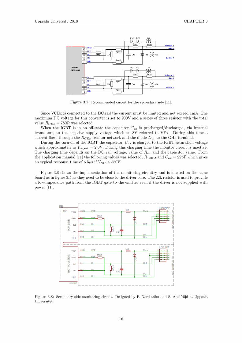
Figure 3.7: Recommended circuit for the secondary side [11].
Since VCEx is connected to the DC rail the current must be limited and not exceed 1mA. Themaximum DC voltage for this converter is set to 900V and a series of three resistor with the totalvalue RCEx = 780Ω was selected.
When the IGBT is in an off-state the capacitor Cax is precharged/discharged, via internaltransistors, to the negative supply voltage which is -8V referred to VEx. During this time acurrent flows through the RCEx resistor network and the diode D11 to the GHx terminal.
During the turn-on of the IGBT the capacitor, Cax is charged to the IGBT saturation voltagewhich approximately is Vce,sat = 2.0V. During this charging time the monitor circuit is inactive.The charging time depends on the DC rail voltage, value of Rax and the capacitor value. Fromthe application manual [11] the following values was selected, R120kΩ and Cax = 22pF which givesan typical response time of 6.5µs if VDC > 550V.
Figure 3.8 shows the implementation of the monitoring circuitry and is located on the sameboard as in figure 3.5 as they need to be close to the driver core. The 22k resistor is used to providea low-impedance path from the IGBT gate to the emitter even if the driver is not supplied withpower [11].
Figure 3.8: Secondary side monitoring circuit. Designed by P. Nordstrom and S. Apelfrojd at UppsalaUniversitet.
16

Uppsala University 2018 CHAPTER 3
3.2.4 Active clamping
The 2SC0108T supports basic active clamping. It is a technique that keeps a transient overvoltagebelow a predefined threshold voltage when the IGBT turns off. When the collector-emitter voltagerises above the transient voltage suppressor, TVS diode breakdown voltage the IGBT is partiallyturned on and kept in linear operation and thus reducing the overvoltage [14]. The full schematicof the high voltage side can be seen in appendix B.
Figure 3.9: Secondary side monitoring circuit. Designed by S. Apelfrojd at Uppsala Universitet.
For 1200V IGBTs with DC-link voltages up to 800V it is recommended to have six 150V TVSdiodes where at least one is bidirectional [11]. Five SMBJ154A-TR and one SMP100MC-160 TVSdiode was chosen and should give good clamping results. It is possible to improve the clampingperformance by reducing Rg,off .
The gate resistors for turn-on and turn-off are separated to set them independently. Thesmallest resistor value allowed is 2Ω [15]. Three 21.5Ω in parallel was chosen which gives a totalof Rg,on,off = 7.17Ω for both turn-on and turn-off resistor.
D5x is a transient voltage suppressor device that protects against high gate-emitter voltages inthe IGBT short-circuit condition.
3.3 DC capacitor
The DC capacitors used are two electrolytic capacitors. The rated voltage is 450V with a capaci-tance of 3300µF. Connected in series they have a rated voltage of 900V. The bleeding resistors arethere to discharge the electric energy stored in the capacitors when the converter is turned off, forsafety reasons. The resistors have a value of 18kΩ and a power rating of 10W.
Figure 3.10 shows how the capacitors are connected in the converter and is viewed from sameangle as the left figure in fig 3.1. The converter has three layers of metal sheets with a insulatingmaterial between them. The top layer is the positive terminal on the DC side of the converterand is connected to the top collectors of the IGBT modules and the positive terminal on one ofthe capacitors. The bottom layer is the negative terminal on the DC side and is connected tothe bottom emittors of the IGBT modules and the negative side on one the other capacitor. Themiddle layer connects the other two layers via the remaining terminals of the capacitors.
17

Uppsala University 2018 CHAPTER 3
Figure 3.10: Illustration of how the DC capacitors are connected and a equivalent circuit.
18

Chapter 4
LabView implementation
The control of the converter is done through LabVIEW which is a visual programming languagefrom National Instruments and their compact real-time embedded industrial controller (cRIO).This consists of a real time (RT) microprocessor controller and I/O FPGA modules [16][17]. Thesetup consited of cRIO-9066 as controller, NI-9401 module for digital I/O and NI-9206 as voltageanalog input.
Figure 4.1 shows the user interface the user sees. The graphs to the left shows the measurementswhen in DC voltage control mode and the right shows it when in active-/reactive-mode. In themiddle there is a visual representation of a HVDC-link and a block diagram of the control strategyalong with RMS-values of the grid voltages and currents. Finally at the bottom the referencevalues are set along with the abillity to tune the PI controllers.
Figure 4.1: User interface for converter control.
4.1 Measurements
The measurement system used in this project comes a from previous student thesis. It measuresvoltages through differential measurements and for the current it uses a current transducer. Thereis a switch where you can choose between the wire running through the current transducer one orsix times. There are two boxes in total labeled ”box A” and ”box B” [18].
In this project it is important that the rectifier measurements are connected to box A and theinverter measurements are connected to box B. The voltage and current measurements of phasea,b and c must also be connected to the U1-U3 and I1-I3 terminals, respectively as seen in figure4.3. The DC bus measurements must always be connected to the U0 and I0 terminals of box A.
19

Uppsala University 2018 CHAPTER 4
Figure 4.2: Measurement box.
Figure 4.3: Data acquisition and calibration.
Table 4.1: Caption
Box A - Rectifier Box B - InverterMeasurement Pin Measurement Pin
Ua AI3 Ua AI19Ia AI2 Ia AI18Ub AI5 Ub AI21Ib AI4 Ib AI20Uc AI7 Uc AI23Ic AI6 Ic AI22
U dc AI1 U dc -I dc AI0 I dc -
In the FPGA there is a ”Data acquisition and calibration” loop that runs at 4 kHz. It retrievesthe measurements from the cRIO NI 9205 pins according to table 4.1. These are represented bythe pink boxes as seen in figure 4.3. The measurements has a voltage range of ±10V so the valuesneeds to be scaled to the correct value. A sub VI implements a linear function, y = kx+m whichallows for scaling and offsetting for all the channels. It can also invert the values. they are thenput into two arrays, one for voltages and the other for currents.
20

Uppsala University 2018 CHAPTER 4
4.2 Bipolar SPWM
Bipolar Sinusoidal pulse width modulation is a technique that compares the three sinusoidal ref-erence signals to a triangular carrier signal in order to create the switching signals as describedin section 2.5. The carrier signal is generated in its own loop. This is a singe-cycle timed loop(SCTL) which can be recognized by its clocks on the side of the loop as seen in figure 4.4. TheSCTL executes all the functions in it during one clock cycle [19]. In this case it is set to the onboard clock that is 40MHz. This makes it possible to generate a signal with a accurate frequencysince the execution time for the function is known.
Figure 4.4: Carrier signal generation.
The function of the triangle wave generation subVI is relatively simple. An increment value isfed into the subVI. In every loop cycle it is added to the previous value and checked if it is in therange of ±1. If this is true it just continuous like the previous loop. If it is false the function checksif the accumulated value is < 0 if that is true nothing happens to the input increment value. If itis false it means that signal is at its top peak and thus the increment value is negated. In short,first it checks if it is in range. If not it checks if it is on its top peak or bottom peak. This meansthat the increment value sets the frequency and its function is given by
increment = fCarrier · 4 · dT (4.1)
Where fCarrier is the wanted frequency and dT is the clock frequency, in this case 40MHz. Fora 4kHz carrier signal a increment value of 0.0004 is selected.
The carrier signal is then compared to either the rectifier reference signals or inverter referencesignals depending on which mode is selected. There will only be an output if the converter isenabled.
The purple boxes in figure 4.5 are connected to the NI 9401 which is a digital module. The topthree are INA for each gate driver and the bottom three is INB as described in chapter 3.2.2
Figure 4.5: PWM signal generation.
21
Uppsala University 2018 CHAPTER 4
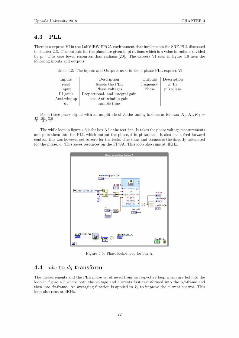
4.3 PLL
There is a express VI in the LabVIEW FPGA environment that implements the SRF-PLL discussedin chapter 2.3. The outputs for the phase are given in pi radians which is a value in radians dividedby pi. This uses fewer resources than radians [20]. The express VI seen in figure 4.6 uses thefollowing inputs and outputs.
Table 4.2: The inputs and Outputs used in the 3-phase PLL express VI
Inputs Description Outputs Descriptionreset Resets the PLL frequency in HzInput Phase voltages Phase pi radians
PI gains Proportional- and integral gainAnti-windup sets Anti-windup gain
dt sample time
For a three phase signal with an amplitude of A the tuning is done as follows: Kp,Ki,KA =12A ,
200A , 200
A .
The while loop in figure 4.6 is for box A i.e the rectifier. It takes the phase voltage measurementsand puts them into the PLL which output the phase, θ in pi radians. It also has a feed forwardcontrol, this was however set to zero for the tests. The sinus and cosinus is the directly calculatedfor the phase, θ. This saves resources on the FPGA. This loop also runs at 4KHz.
Figure 4.6: Phase locked loop for box A.
4.4 abc to dq transform
The measurements and the PLL phase is retrieved from its respective loop which are fed into theloop in figure 4.7 where both the voltage and currents first transformed into the αβ-frame andthen into dq-frame. An averaging function is applied to Vd to improve the current control. Thisloop also runs at 4KHz.
22

Uppsala University 2018 CHAPTER 4
Figure 4.7: abc to dq transform.
The subVI in figure 4.8 implements the Clarke transform given in equation 2.6. It does it in aresourceful way by minimizing the use of multiplications which are resource demanding.
Figure 4.8: Clarke transform subVI.
The subVI in figure 4.9 implements the Park transform given in equation 2.9. It also doesit in a resourceful way by taking the already calculated values for Sin(θ) and Cos(θ) instead ofcalculating it again every time.
Figure 4.9: Park transform subVI.
4.5 Current control
The methods from chapter 2.4 was implemented into LabVIEW. In the program, one can chooseto either control the active-/reactive power using the id and iq current control or the DC voltage.They were programmed on the FPGA and RT, respectively due resource limitations on the FPGAand ease of testing.
4.5.1 id and iq current control
With the dq- currents and voltages the controller can be implemented. Since the compensators infigure 2.6 are identical the same proportional and integral values are used for both of them. L andid,ref&iq,ref is chosen in the RT front panel. The Figure 4.10 implements the equations given in2.18.
23

Uppsala University 2018 CHAPTER 4
Figure 4.10: Data from FPGA and current control for the inverter.
The PI compensator used is designed to use as few resources on the FPGA as possible. Itdoes not however have a anti-windup mechanism so the controller runs the risk of running out ofcontrol. The subVI for the PI compensator is shown in figure 4.11. The control is placed in a forloop that runs once for each compensator.
Figure 4.11: PI compensator SubVI for real-/reactive-power control.
4.5.2 DC voltage control
As mentioned the DC voltage control runs on the RT. That means that we need to exchange datawith the FPGA. That is done through the read/write block to the left in figure 4.12. The neededinput parameters described in 2.4 are then given to the DC controller subVI where the controltakes place.
24

Uppsala University 2018 CHAPTER 4
Figure 4.12: Data from FPGA and current control.
Figure 4.13 is the same as the id and iq current control with the addition of the DC voltagecompensator described in chapter 2.4.1. It utilizes a saturation block limiting the maximum id,refalong with a anti-windup. The other two compensator also has a saturation block that limits themodulation signals to stay within ±VDC
2 [8].
Figure 4.13: DC voltage control subVI.
The modulation signals are then fed back into the FPGA. Putting the controller on the RTinstead of the FPGA is not the optimal solution as the FPGA runs at a faster clock speed and isbetter at timing/syncing [16].
4.6 dq to abc transform
From the current control the reference voltages are obtained in dq reference frame and are dividedby 1
2VDC as mentioned in 2.18. They are then transformed into the abc reference frame with arange of ±1. This is displayed in figure 4.14.
25

Uppsala University 2018 CHAPTER 4
Figure 4.14: dq to abc transform
The subVI in figure 4.15 implements the inverse Park transform given in equation 2.11.
Figure 4.15: Inverse Park transform subVI.
The subVI in figure 4.16 implements the inverse Clarke transform given in equation 2.7. It doesit in a resourceful way by minimizing the use of multiplications which are resource demanding.
Figure 4.16: Inverse Clarke transform subVI.
26

Uppsala University 2018 CHAPTER 4
4.7 Converter safety
It is important to always have some sort of protection to avoid damaging equipment or harmingpersons. Since the converters will be used in a laboratory by users that might not have a fullunderstanding of the equipment’s limitations and function a safety system is in put in place. Thissystem monitors the peak grid current and the DC bus voltage. figure 4.17 shows the system inplace. It is put in a loop that is set to run as fast as possible in order to detect a fault as fastas possible. The measurements are compared to a chosen maximum value. If any of these aretriggered a s-r latch is set and disables the converter. In order to start the converter again thelatch must be reset. The ”Enable converter” which is the main ON/OFF switch must also be Truein order for the converter to turn on. ”Converter Active” is the output from this loop and fed intothe SPWM generation loop.
Figure 4.17: Converter safety.
This is a relatively simple safety feature and should not be fully relied on. The capacitors canhold a lot of charge and there are a lot of exposed areas where a person can be struck and in worstcase be killed by an electric shock. There are bleeding resistors in place which dissipates the chargein the capacitor so they don’t pose as a threat when it is turned off.
Like with any electrical equipment, the converters should always be approached with caution.
4.8 Real Time
All the measurements and calculations done on the FPGA is transferred to the real time throughthe FIFO. Figure 4.18 can be called the producer loop. It requests a defined set of data and whenthe FIFO meets this condition the data is released and sorted. It does this for all 30 measurementsand calculations. These are then transferred to the consumer loop in figure 4.19.
The amount of data the user demands defines how many periods will be shown on the graphs.The FIFO operates at 4KHz this means that it reads 4000 data points every second. If two periodsof a 50Hz signal is to be displayed 160 data points is wanted. This is then multiplied by the amountof data channels, which is 30. So, to show two periods the amount of data requested from theFIFO should be 160 · 30 = 4800.
27

Uppsala University 2018 CHAPTER 4
Figure 4.18: Data from FIFO.
The consumer loop in figure 4.19 takes this data and does RMS calculations for the gridmeasurements. It also displays the data on graphs on the front panel as seen in figure 4.1.
Figure 4.19: Data from FIFO.
28

Chapter 5
Results
This section presents the testing of the bidirectional converter in DC voltage control and id andiq current control over a resistive load. The tests were conducted in a lab environment where theyalso will be used in course laboratory work.
5.1 Setup
The setup used for testing is shown in figure 5.1. The voltage supply in the bottom left of thepicture and can supply both a variable DC voltage and three phase AC voltage along with fixedvoltages. It is connected to the grid via a transformer that brings down the line-to-line voltagefrom 400V to 230V. The voltage supply is also equipped with breakers up to 10A.
Depending on the selection of controller type, DC voltage control or active-/reactive powercontrol it is connected to three phase AC supply or DC supply, respectively. The measurementboxes are then connected to the voltage supply for measurements. Again, box A or box B is useddepending on the type of controller used as mentioned in chapter 4.1. From the box it is connectedto the line inductor, L. This is labeled as a ”load inductor” and has a variety of configurations.Attempts to estimate the inductance were made and are shown in table 5.1. The line inductor isconnected to the AC side of the converter.
Since the tests in this project never connected to the grid, a resistive load was used for testingpurposes. It is located in the center of figure 5.1, the load is a variable three phase resistive load. Tothe far right is the computer on which the user interface is displayed. The computer is connectedto the compactRIO via ethernet.
Table 5.1: Rating of the equipment used for testing.
item ratingVDC 0-220VVl−l 0-230V
L 0.072-0.8HRload 0-300Ω
29

Uppsala University 2018 CHAPTER 5
Figure 5.1: Laboratory test setup.
5.2 id and iq current control test
Two tests were conducted for id and iq current control. One with id = 2 and iq = 0 and anotherwith a step response of id = 1 − 2 and iq = 0.
A DC voltage was connected to the converter which in turn was connected to a load. Since theconverter is not connected to the grid a simulated three-phase grid was implemented into theFPGA that the PLL could track. This may effect the results since there is no real grid for theconverter to relate to.
Table 5.1 shows the parameters for the testing results in figure 5.3. Where VDC and IDC is thesupply voltage and vrms and vrms is the load voltage and load current, respectively. From this weget that the input power is 93.6W and the output power is 88.2W which results in a 94% efficiencyfor this test. Figure 5.2 shows the converter voltage at one of its AC output terminal.
Table 5.2: Values for id and iq current control.
item rating item ratingVDC 117V Rload 15ΩIDC 0.5A Idref 2vrms 21V Iqref 0irms 1.4A kp 240
L 0.28H ki 3
0 0.01 0.02 0.03 0.04 0.05 0.06 0.07 0.08
Time [S]
-50
-40
-30
-20
-10
0
10
20
30
40
50
[V]
Figure 5.2: Voltage at the on of the converter AC outputs.
30

Uppsala University 2018 CHAPTER 5
Figure 5.3 shows the plots from the test with id = 2 and iq = 0 in steady state and they are; a)is the load voltage and as it can be seen there is a lot disturbances which will manifest themselvesthrough out the control. b) shows the load current, the peak is at 2A which is the reference idcurrent since the amplitude variant of the reference frame transform is used. c) Shows the loadvoltages in dq-frame and the disturbances from a) are visible, there are high fluctuations of about±6V for both Vd and Vq. d) shows the load currents in dq-frame and it has the desired outputsfrom the reference values. e) Is the PLL and it tracks the simulated three-phase system. It canbe observed that phase a (blue) in a) is at its peak when θ is zero. f) Shows the three modulationsignals and they are not over modulated. They do however jump to zero at times. It is unclearwhere this is introduced into the system. It can be due to the programming of the simulated grid.
0 0.005 0.01 0.015 0.02 0.025 0.03 0.035 0.04
Time [S]
-40
-30
-20
-10
0
10
20
30
40
Lo
ad
vo
lta
ge
[V]
(a)
0 0.005 0.01 0.015 0.02 0.025 0.03 0.035 0.04
Time [S]
-2.5
-2
-1.5
-1
-0.5
0
0.5
1
1.5
2
2.5
Lo
ad
cu
rre
nt[
V]
(b)
0 0.005 0.01 0.015 0.02 0.025 0.03 0.035 0.04
Time [S]
-10
-5
0
5
10
15
20
25
30
35
40
Vd
& V
q
(c)
0 0.005 0.01 0.015 0.02 0.025 0.03 0.035 0.04
Time [S]
-0.5
0
0.5
1
1.5
2
2.5
Id &
Iq
(d)
0 0.005 0.01 0.015 0.02 0.025 0.03 0.035 0.04
Time [S]
-1
-0.8
-0.6
-0.4
-0.2
0
0.2
0.4
0.6
0.8
1
Th
eta
(e)
0 0.005 0.01 0.015 0.02 0.025 0.03 0.035 0.04
Time [S]
-1
-0.8
-0.6
-0.4
-0.2
0
0.2
0.4
0.6
0.8
1
ma
. m
b a
nd
mc
(f)
Figure 5.3: a) load voltage b) load current c) Vd Vq d) Id Iq e) Theta from PLL f) modulationsignals ma mb mc.
31

Uppsala University 2018 CHAPTER 5
Figure 5.4 shows when a step response test was conducted with id going from 1A to 2A andiq = 0. As it can be seen when the step is initialized at 3s the power drops to about 20W and isthen in steady state right after 4s. Although the controller is responsive there is large disturbancesin the power.
0 0.5 1 1.5 2 2.5 3 3.5 4
Time [S]
0
20
40
60
80
100
120
P [W
]
Figure 5.4: Power Step response for id = 1− 2 and iq = 0.
5.3 DC voltage control test
Table 5.3 shows the parameters for the DC voltage controller test. VDC and IDC is the DC valueswhen the converter is turned off and act as an passive rectifier. vrms and irms is the grid voltageand current. L is the estimated line inductance and VDCref is the value the converter regulatesthe DC voltage at. The pi controller values are for the inner and outer control, respectively.
Table 5.3: Values for DC voltage control.
item ratingVDC 50VIDC 0.15Avrms 23Virms 0.15A
L 0.28HRload 300ΩVDCef 90kp 240 and 0.004ki 3 and 0.003
Figure 5.5 shows the DC voltage at 90V and in steady state with the parameters from table 5.3.With this setup it was possible to comfortably boost the DC voltage up to 240V. After that it hadproblems keeping the voltage steady and current draw started to get to high for the equipment.Figure 5.6 shows the plots from the test and they are; a) is the grid voltage and as it can be seenthere is some disturbances introduced when the converter is turned on. b) shows the grid current,it is in phase with the grid voltage which means that only real power is absorbed from the grid.c) shows the grid voltages in dq-frame. The average is taken on Vd so the value presented is veryconsistent while Vq has more disturbances but is at zero which means that the PLL is workingcorrectly. d) Is the grid current in dq-frame and it shows iq at zero which grants unity powerfactor. e) Is the PLL which tracks the grid. It can be observed that phase a (blue) in a) is at itspeak when θ is zero. f) Shows the modulation signals and they are not over modulated.
32

Uppsala University 2018 CHAPTER 5
0 0.005 0.01 0.015 0.02 0.025 0.03 0.035 0.04
Time [S]
85
86
87
88
89
90
91
92
93
94
95
Vd
c
Figure 5.5: DC voltage at steady state.
0 0.005 0.01 0.015 0.02 0.025 0.03 0.035 0.04
Time [S]
-40
-30
-20
-10
0
10
20
30
40
Grid
vo
lta
ge
[V
]
(a)
0 0.005 0.01 0.015 0.02 0.025 0.03 0.035 0.04
Time [S]
-0.8
-0.6
-0.4
-0.2
0
0.2
0.4
0.6
0.8
Grid
cu
rre
nt
[A]
(b)
0 0.005 0.01 0.015 0.02 0.025 0.03 0.035 0.04
Time [S]
-5
0
5
10
15
20
25
30
35
Vd &
Vq
(c)
0 0.005 0.01 0.015 0.02 0.025 0.03 0.035 0.04
Time [S]
-0.1
0
0.1
0.2
0.3
0.4
0.5
0.6
0.7
Id &
Iq
(d)
0 0.005 0.01 0.015 0.02 0.025 0.03 0.035 0.04
Time [S]
-1
-0.8
-0.6
-0.4
-0.2
0
0.2
0.4
0.6
0.8
1
Th
eta
(e)
0 0.005 0.01 0.015 0.02 0.025 0.03 0.035 0.04
Time [S]
-0.8
-0.6
-0.4
-0.2
0
0.2
0.4
0.6
0.8
ma
, m
b a
nd
mc
(f)
Figure 5.6: a) grid voltage b) grid current c) Vd and Id d) id and iq e) PLL f) modulation signalsma, mb and mc.
33

Uppsala University 2018 CHAPTER 5
Figure 5.7 shows when the converter starts up. In the beginning it acts as a passive rectifierand is stable at 50V. When it starts the voltage quickly drops to zero and then rises and overshootswith about 50V to 140V until it settles at the desired 90V. The whole start up sequence takesabout 13 seconds.
0 2 4 6 8 10 12
Time [S]
0
50
100
150
Vdc
Figure 5.7: Start up for DC voltage control.
34

Chapter 6
Conclusions and future work
In this thesis, a two level bidirectional VSC for a laboratory test setup was designed and built. Acontrol system was also developed to enable the control of active-/reactive power flow along witha DC voltage control.
The converter was tested both in inverter and rectifier mode connected to a resistive load.Start-up sequences and power flow step changes was also analyzed with promesing results.
Some conclusions that can be drawn from the design and construction, programming of the controlsystem and the testing, are the following
• The converter constructed was a copy of an already existing and functioning converter. Thebehaviour of the two was found to be similar. Tests showed that the converter was workingaccording to the wanted specifications and thus, it can be used for laboratory use.
• Using the compactRIO and LabVIEW offers a reliable and convenient method when mea-suring and processing data. The responsiveness of the control might be affected dependingon if it placed on the FPGA or the real time microprocessor.
• The converter is able to work as an inverter and regulate the current flow to resistive loadusing a simulated grid. A lot of harmonics is introduced to the AC load voltage and thereare large fluctuations in the load power.
• The converter is also able to function as an rectifier and regulate the DC voltage over anresistive load. It has the ability to boost the voltage DC voltage several magnitudes but islimited when trying to deliver a larger effect. The start up of the converter delivers a largevoltage spike.
There is a wide range of other uses for a VSC converter and for the existing system there isroom for great improvements. Some suggested future works are the following.
• Improve the control and connect the converter to the grid to fully test the ability of controllingthe active-/reactive power flow.
• Connect two converters back-to-back and thus forming a HVDC-link and connect them tothe grid.
• Develop a laboratory test for students where they can observer the behaviour of the converterwhen changing parameters such as, PI controller constants, carrier frequency, DC voltages,etc.
35

Bibliography
[1] K. Sharifabadi et al. Design, Control, and Application of Modular Multilevel Converters forHVDC Transmission Systems. Wiley - IEEE. Wiley, 2016. isbn: 9781118851562.
[2] J. Arrillaga, Y.H. Liu, and N.R. Watson. Flexible Power Transmission: The HVDC Options.Wiley, 2007. isbn: 9780470511855. url: https://books.google.se/books?id=3LZ-
284jCf4C.
[3] Markus Gabrysch. Lecture slides. Inverter Design with Applications. The Faculty Board ofScience and Technology Uppsala University. 2017.
[4] Amirnaser Yazdani and Reza Iravani. Voltage-sourced converters in power systems: modeling,control, and applications. John Wiley & Sons, 2010.
[5] W. C. Duesterhoeft, M. W. Schulz, and E. Clarke. “Determination of Instantaneous Currentsand Voltages by Means of Alpha, Beta, and Zero Components”. In: Transactions of theAmerican Institute of Electrical Engineers 70.2 (July 1951), pp. 1248–1255. issn: 0096-3860.doi: 10.1109/T-AIEE.1951.5060554.
[6] R. H. Park. “Two-reaction theory of synchronous machines generalized method of analysis-part I”. In: Transactions of the American Institute of Electrical Engineers 48.3 (July 1929),pp. 716–727. issn: 0096-3860. doi: 10.1109/T-AIEE.1929.5055275.
[7] S. Golestan, J. M. Guerrero, and J. C. Vasquez. “Three-Phase PLLs: A Review of RecentAdvances”. In: IEEE Transactions on Power Electronics 32.3 (Mar. 2017), pp. 1894–1907.issn: 0885-8993. doi: 10.1109/TPEL.2016.2565642.
[8] OTTERSTEN ROLF. On Control of Back-to-Back converters and Sensorless Induction Ma-chine Drives. PhD Thesis, Department of Electric Power Engineering, Chalmers Universityof Technology, Goteborg, Sweden. 2003.
[9] Sylvain LECHAT SANJUAN. Voltage Oriented Control of Three-Phase Boost PWM Con-verters. Department of Electric Power Engineering, Chalmers University of Technology,Goteborg, Sweden. 2010.
[10] Fuji Electric Device Technology Co. 93193.pdf. http://www.farnell.com/datasheets/93193.pdf. 2005.
[11] Power Integrations Switzerland GmBH. 2SC0108T Preliminary Description and ApplicationManual. Jan. 2018.
[12] Power Integrations Switzerland GmBH. Application with SCALETM-2 and SCALETM-2+Gate Driver Cores. Apr. 2016.
[13] CD40106B CMOS Hex Schmitt-Triggers Inverters datasheet (Rev. F). http://www.ti.com/lit/ds/symlink/cd40106b.pdf. Mar. 2017.
[14] Inc Littelfuse. littelfuse tvs diode protection for vfds igbt inverters.pdf. https://www.littelfuse.com/~/media/electronics/application_notes/littelfuse_tvs_diode_protection_
for_vfds_igbt_inverters.pdf. 2016.
[15] Power Integrations Switzerland GmBH. 2SC0108T2F1(C)-17 Data Sheet. https://gate-driver.power.com/sites/default/files/product_document/data_sheet/2SC0108T2F1-
17.pdf. 2018.
[16] National instruments. NI LabVIEW Real-Time and FPGA - National Instruments. ftp:
//ftp.ni.com/pub/branches/uk/handson_followup/handson_tasters.
36

Uppsala University 2018 CHAPTER
[17] CompactRIO Systems - National Instruments. http://www.ni.com/sv-se/shop/compactrio.html.
[18] Jonas Lindstrom. Measurement system for laboratory use: For studies in electrical science.2015.
[19] Single-Cycle Timed Loop FAQ for the LabVIEW FPGA Module - National Instruments.https://knowledge.ni.com/KnowledgeArticleDetails?id=kA00Z000000P8sWSAS&l=sv-
SE. July 2018.
[20] 3-Phase PLL Express VI - LabVIEW 2016 FPGA Module Help - National Instruments.http://zone.ni.com/reference/en-XX/help/371599M-01/lvfpga/fpga_3phase_pll/.June 2016.
37

Appendix A
Low voltage side schematic
VC
E
RE
F
GL
VE
GH
Rvc
e
Gof
f
Gon
VE
VC
E
RE
F
GL
VE
GH
Gon
VE
Gof
f
Rvc
e
High Side Driver HV Low Side Driver HV
Inpu
ts w
ith p
rote
ctio
n an
d sh
ort p
ulse
reje
ctio
n
Top
Side
Botto
m S
ide
Erro
r out
- N
OT(
SO1
OR
SO
2) (N
orm
al L
ow)
Supp
ly In
put w
ith s
urge
pro
tect
ion
and
smal
l buf
fer
Driv
er D
e-co
uplin
g
Pin
Hea
d IN
VC
C3,
4, 5
Sup
ply
IdPi
nTy
pe
GN
D1,
5,6,
9S
uppl
yIN
A2
Con
trolle
rIN
B10
Con
trolle
rD
F8
Indi
cato
r
Info
15V
1W
Gro
und
Driv
er s
igna
l, 15
V 5
mA
Driv
er s
igna
l, 15
V 5
mA
Err
or o
ut, 1
5V (D
efau
lt Lo
w)
Driv
er S
ettin
gsP
inH
ead
Hig
hSid
e an
d Lo
wS
ide
Dire
ct M
ode
- Con
nect
Mod
e-1
and
Mod
e-2
Com
plim
enta
ry M
ode
- Con
nect
Mod
e-3
and
Mod
e-4
(Rec
omm
ende
d)
MM
XIII
Ver
sion
4 R
ev.2
013-
10
MM
XIII
2013
-10-
23IG
BT D
river
UU
- El
ektri
cite
tslä
raP.
Nor
strö
mS.
Apel
fröjd
TOP SIDE BOTTOM SIDE
LVH
V
4010
6D40
106D
4010
6D40
106D
4010
6D
+15V
GN
D
GND
GN
D
+15V
GN
D
+15V
GN
D
GND
GN
D
GND
GN
D
+15V
GND
+15V
GND
+15V
+15V+15V
GND
GND
BC84
7
+15V GN
D
RTH
2
22K_2
CA
2
RA
2
D12
RTH
1
22K_1
CA
1
RA
1
D11
HIG
HS
IDE
135
24679
810
CO
RE
2SC
0108
T
GN
DG
ND
INA
INA
INB
INB
VC
CV
CC
TBTB
SO2
SO2
SO1
SO1
MO
DM
OD
GH
1G
H1
VE
1V
E1
GL1
GL1
RE
F1R
EF1
VC
E1
VC
E1
GH
2G
H2
VE
2V
E2
GL2
GL2
RE
F2R
EF2
VC
E2
VC
E2
LOW
SID
E 135
24679
810
IC1A
12
IC1B
34
IC1D
98
IC1E
1110
IC1F
1312
IC1PVDD VSS
714
R1
R2
R3
C1
C2
C3
C4
RB
CM RM
R4
R5
R6
C5
CD
D6
D7
IN
1 3 5
2 4 67 9
8 10
D1
C7
LED1
R7
T1
R8
R9
ER
RO
R_O
UT_
SO
1_O
R_S
O2
+
Figure A.1: Designed by P. Nordstrom and S. Apelfrojd at Uppsala Universitet.
38

Appendix B
High voltage side schematic
MM
XIII
2013
-10-
23D
river
_Mou
ntU
U -
Ele
ktric
itets
lära
S.A
pelfr
öjd
GND
VCC
VCCVCC
GNDGND
GNDGND
OPA
642N
VCC
VCC
GN
DG
ND
GN
D
VCC
MO
UN
T-PA
D-R
OU
ND
4.3
LOW
SID
E 135
24679
810
HIG
HSI
DE
135
24679
810
SV3
135
24679
810
X1-
2
X1-
3
X1-
4X
1-5
X1-
6X
1-7
X1-
8
X1-
9X1-
G
X1-
1
D51D52
D31
-1D
31-2
D31
-3D
41-1
D41
-2D
41-3
D32
-1D
32-2
D32
-3D
42-1
D42
-2D
42-3
RG
_ON
1-1
RG
_ON
1-3
RG
_ON
1-2
RG
_OFF
1-1
RG
_OFF
1-2
RG
_OFF
1-3
RG
_OFF
2-1
RG
_OFF
2-2
RG
_OFF
2-3
RG
_ON
2-1
RG
_ON
2-2
RG
_ON
2-3
RVC
E1-1
RV
CE
1-2
RVC
E2-1
RV
CE
2-2
RVC
E2-3
RVC
E1-3
C_L
S
G_L
S
E_L
S
G_H
S
E_H
S
C_H
S
IC1
431
5 2
C1
C2
R1
NTC 1 2
H1
E_HS1
G_O
N1
G_O
FF1
G_O
N2
G_O
FF2
E_I
GB
T1
E2 C1
C2/
E1
S1S2 ERR
OR
SHIE
LD
A B C D
12
34
56
A B C D
12
34
56
Figure B.1: Designed by S. Apelfrojd at Uppsala Universitet.
39