a zvzcs full bridge converter with high voltage gain by solar energy source
TRANSCRIPT
8/11/2019 A Zvzcs Full Bridge Converter With High Voltage Gain by Solar Energy Source
http://slidepdf.com/reader/full/a-zvzcs-full-bridge-converter-with-high-voltage-gain-by-solar-energy-source 1/7
INTERNATIONAL JOURNAL OF SCIENTIFIC & TECHNOLOGY RESEARCH VOLUME 3, ISSUE 4, APRIL 2014 ISSN 2277-8616
203IJSTR©2014www.ijstr.org
A Zvzcs Full Bridge Converter With High VoltageGain By Solar Energy Source
Nimmy Berchmans, V. Geetha
Abstract: This paper proposes a ZVZCS asymmetrical full-bridge converter with high-voltage gain by different loads. The proposed converter featureshigh-voltage gain, fixed switching frequency and clamped voltages across power switches and output diodes. The control of the converter isimplemented with the asymmetrical pulse width modulation technique. The converter achieves zero-voltages witching (ZVS) of all power switches andZero-current switching (ZCS) of output diodes. The energy shortage and the atmosphere pollution have led to more researches in renewable sources ofenergy. In this paper, PV module is modelled using Matlab/Simulink. The modeled PV cell act as the dc input source for the converter. The computesimulation of the converter is done using MATLAB/SIMULINK and is interfaced with the mathematical model of PV cell and various waveforms arepresented in the paper.
Index Terms: DC –DC converter, high-voltage gain, zero-voltage switching (ZVS), zero-current switching (ZCS), PV module.————————————————————
1) INTRODUCTIONRecently, the demand for dc/dc converters with high voltagegain has increased because they are required as an interfacesystem between the low voltage sources and the high voltageload which requires higher voltage. This high voltage gain dcto dc converter find applications in electric vehicles,uninterruptible power supplies, fuel cells, and photovoltaicsystems [1] –[6]. A conventional boost converter is often usedin step-up applications due to its simple structure and lowcost. However, it is not suitable for high step-up applications.This is because the conventional boost converter requires anextreme duty cycle to obtain high-voltage gain and its voltagegain is limited due to its parasitic components [11]. Thereverse-recovery problem of the output diodes is anotherimportant factor in dc/dc converters with high voltage gain. Inorder to remedy these problems, high step-up dc –dcconverters using coupled inductors have been suggested in[9] and [10]. However, they have parasitic oscillations acrossthe switches and diodes. The current-fed converters are oftenused in high step-up applications due to their inherent lowinput current ripple characteristic and high-voltage gain [8],[12] but here the voltage stresses of the switches are serious.In order to clamp the voltages across the switches andprovide zero-voltage switching (ZVS) features, activesnubbers are often employed. The snubbers requireadditional switches and cause additional conduction losses.As a result, the system efficiency decreases. To remedythese problems, many topologies have been proposed that isthe voltage-fed converters such as phase-shift full-bridge(PSFB) converters, which are widely used, show low-voltagestress of the switching devices.
However, they have some drawbacks including largeconduction loss due to circulating current, duty cycle loss, andthe voltage spikes across output rectifier. In some of themauxiliary snubber circuits are employed to suppress thevoltage spikes at the secondary side. However, the
complexity and the overall cost are increased while thesystem efficiency decreases due to the additional circuits. Inorder to overcome these problems, an asymmetrical fulbridge converter with high-voltage gain is proposed andshown in Fig. 1. The APWM technique is applied to converteto eliminate switching losses and maintain low conductionloss. The limitation of the maximum duty cycle disappears inthis topology. The converter features high-voltage gain, fixedswitching frequency, soft-switching operations of all poweswitches and output diodes, and clamped voltages acrosspower switches and output diodes. The reverse recoveryproblem of the output diodes is significantly alleviated due toan additional inductor at the secondary side. Therefore, thisconverter shows high efficiency and it is suitable for highvoltage applications. The dc to dc converters are required asan interface system between photovoltaic systems, fuel cellsand electric vehicles. Increasing population growth andeconomic development are accelerating the rate at whichenergy and in particular electrical energy is being demandedIn this highly energy concerned world, focus has been shiftedto utilize renewable sources of energy. This has motivated tointerface the asymmetrical full bridge converter with a lowvoltage source and this has resulted in focusing to solarenergy. In this paper a zvzcs asymmetrical full bridgeconverter with high voltage gain interfaced with solar energyand also this circuit is implemented with different types oloads. All methods of electricity generation haveconsequences for the environment, so meeting this growth indemand, while safe- guarding the environment poses agrowing challenge. Renewable energy technology offers thepromise of clean, abundant energy gathered from selfrenewing resources such as sun, wind, water, earth and plantRenewable energy technology offer important benefitscompared to those of conventional energy sources. Thesetypes of systems, which are not connected to the main utilitygrid, are also used in stand-alone applications and operateindependently and reliably. The best applications for thesesystems are in remote places, such as rural villages, intelecommunications, etc.
_____________________________
Nimmy Berchmans, Mrs.V.Geetha
ME-Scholar, Power Electronics & industrial drives, Asst. Prof EEE Dept

8/11/2019 A Zvzcs Full Bridge Converter With High Voltage Gain by Solar Energy Source
http://slidepdf.com/reader/full/a-zvzcs-full-bridge-converter-with-high-voltage-gain-by-solar-energy-source 2/7
INTERNATIONAL JOURNAL OF SCIENTIFIC & TECHNOLOGY RESEARCH VOLUME 3, ISSUE 4, APRIL 2014 ISSN 2277-8616
204IJSTR©2014www.ijstr.org
2)ANALYSIS OF ZVZCS FULL-BRIDGE
CONVERTER WITH HIGH VOLTAGE GAIN
The circuit diagram of the converter with high-voltage gain isshown in fig 1. The converter has four power switches S1through S4. There is a clamping capacitor Cc between topside switches S1 and S3 of two switch bridges [21]. Thevoltages across the switches S1 and S2 in the first bridge areconfined to the input voltage Vin. The clamping capacitor Cc
can clamp the voltages across the switches S3 and S4 in thesecond bridge. The output stage of the converter has avoltage doubler structure that consists of the secondarywinding N2 of the transformer T, the serial inductor Ls, theoutput capacitors Co1, and Co2, and the output diodes Do1and Do2.In the voltage doubler structure, the voltage gainincreases and the voltage stresses of the output diodes areconfined to the output voltage Vo without any auxiliarycircuits.
Fig -1: Circuit diagram
Fig. 2 shows the equivalent circuit of the converter. Thediodes D1 through D4 are the intrinsic body diodes of allswitches. The capacitors C1 through C4 represent theirparasitic output capacitances. The transformer T is modeledas the magnetizing inductance Lm and the ideal transformerthat has a turn ratio of 1: n (n = N2 /N1). Its leakageinductance is included in the serial inductor Ls.
Fig- 2:-Equivalent circuit of the converter
To simplify the analysis, it is assumed that the clampingcapacitor Cc has a large value and the voltage across Cc isconstant as VC under a steady state. Similarly, the outputcapacitor voltages are assumed to be constant as VO 1 andVO 2, respectively. The theoretical waveforms of theproposed converter are shown in Fig. 3. The switch S1 (S4)and the switch S2 (S3) are operated asymmetrically and theduty cycle D is based on the switch S1 (S4). A small delay
between driving signals for S1 (S4) and S2 (S3) is a deadtime for the switches. It prevents cross conduction and allowsZVS. The converter consist of four modes of operation asshown in Fig. 4.Before t0 , the switches S2 and S3 , and theoutput diode Do 1 are conducting. At t0, the magnetizingcurrent im and the secondary current is arrive at theiminimum values Im2 and −IDo1, respectively.
Mode 1 [t0, t1]: At t0, the switches S2 and S3 are turnedOFF. Then, the energy stored in the magnetic componentsstarts to charge/discharge the parasitic capacitances C1through C4 .Therefore, the voltages vS 2 and vS 3 start torise from zero. Similarly, the voltage vS 4 starts to fall fromVin + Vc and the voltage vS 1 starts to fall from Vin . Since al
the parasitic output capacitances C1 through C4 are verysmall, this transition time interval is very short and it is ignoredin Fig. 3. When the voltages vs 1 and vs 4 arrive at zero, theibody diodes D1 and D4 are turned ON. Then, the gate signalsare applied to the switches S1 and S4. Since the currentshave already flown through D1 and D4 and the voltages vs1and vs 4 are clamped as zero before the switches S1 and S4are turned ON, zero-voltage turn-ON of S1 and S4 isachieved. With the turn-ON of S1 and S4, the primary voltageVP across Lm is Vin.
Fig. 3:- Theoretical waveforms
.

8/11/2019 A Zvzcs Full Bridge Converter With High Voltage Gain by Solar Energy Source
http://slidepdf.com/reader/full/a-zvzcs-full-bridge-converter-with-high-voltage-gain-by-solar-energy-source 3/7

8/11/2019 A Zvzcs Full Bridge Converter With High Voltage Gain by Solar Energy Source
http://slidepdf.com/reader/full/a-zvzcs-full-bridge-converter-with-high-voltage-gain-by-solar-energy-source 4/7
INTERNATIONAL JOURNAL OF SCIENTIFIC & TECHNOLOGY RESEARCH VOLUME 3, ISSUE 4, APRIL 2014 ISSN 2277-8616
206IJSTR©2014www.ijstr.org
Module photo-current:
Iph Iscr+Ki (T-298]*λ/1000 (8)
Module reverse saturation current:
Irs=Iscr/ [exp (qVoc/NskAT)-1] (9)
The module saturation current I0 varies with the celltemperature, which is given by
Io=Irs[T/Tr]3 exp[q*Ego/Bk{(1/Tr)-(1/T)}] (10)
The current output of PV module is
pv=Np*Iph-Np*Io[exp{q*(Vpv+IpvRs)/NsAkT}-1 (11)
Where Vpv = Voc, Np = 2 and Ns = 72
First step is to convert the module operating temperaturegiven in degrees Celsius to Kelvin shown in Fig:-5
Fig 5:- Circuit under subsystem 1
Then find module photo current, module reverse saturationcurrent Irs, module saturation current Io and finally currentoutput of PV module Ipv. The final model is shown in Figure6. The workspace is added to measure Ipv, Vpv, Ppv in thismodel.
Fig 6:- Simulink model of PV module
The final model takes irradiation, operating temperature inCelsius and module voltage as input and gives the outputcurrent Ipv and output voltage Vpv. In the paper, the PVmodule is modelled using the above eqns and interfaced withasymmetrical full bridge converter ie, solar panel is made asthe dc source of the converter.
4) SIMULATION AND RESULTS The converter of Fig.1 with solar energy source is simulatedusing MATLAB/SIMULINK for the following input and outpudata specifications.
a) Input voltage, Vin: 48Vb) Output voltage, Vo: 368Vc) full-load power, Pout: 150d) Switching frequency ,fs : 74 kHz.
As per the analysis, the voltage gain is 8 and turns ratio of 3and Ls (90μH) and Lm (132μH). The simulated circuit diagramof the converter with R, RL, RLE loads by PV module as itssource are shown in fig 7, 9&11. The output voltages areshown in fig 8, 10, 12.
Fig-7:- Simulated circuit diagram of zvzcs asymmetrical fullbridge converter with solar energy as dc source
Time in sec
Fig-8:- Output voltage waveform for R load
8/11/2019 A Zvzcs Full Bridge Converter With High Voltage Gain by Solar Energy Source
http://slidepdf.com/reader/full/a-zvzcs-full-bridge-converter-with-high-voltage-gain-by-solar-energy-source 5/7
INTERNATIONAL JOURNAL OF SCIENTIFIC & TECHNOLOGY RESEARCH VOLUME 3, ISSUE 4, APRIL 2014 ISSN 2277-8616
207IJSTR©2014www.ijstr.org
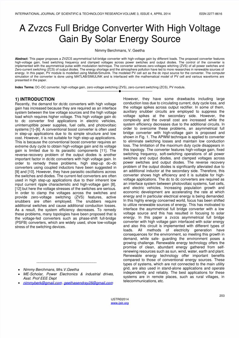
Fig-9:-Simulated circuit diagram of converter with RL load.
Fig-10:- Output voltage waveform for RL load
Fig-11:-Simulated circuit diagram of converter with RLE load.
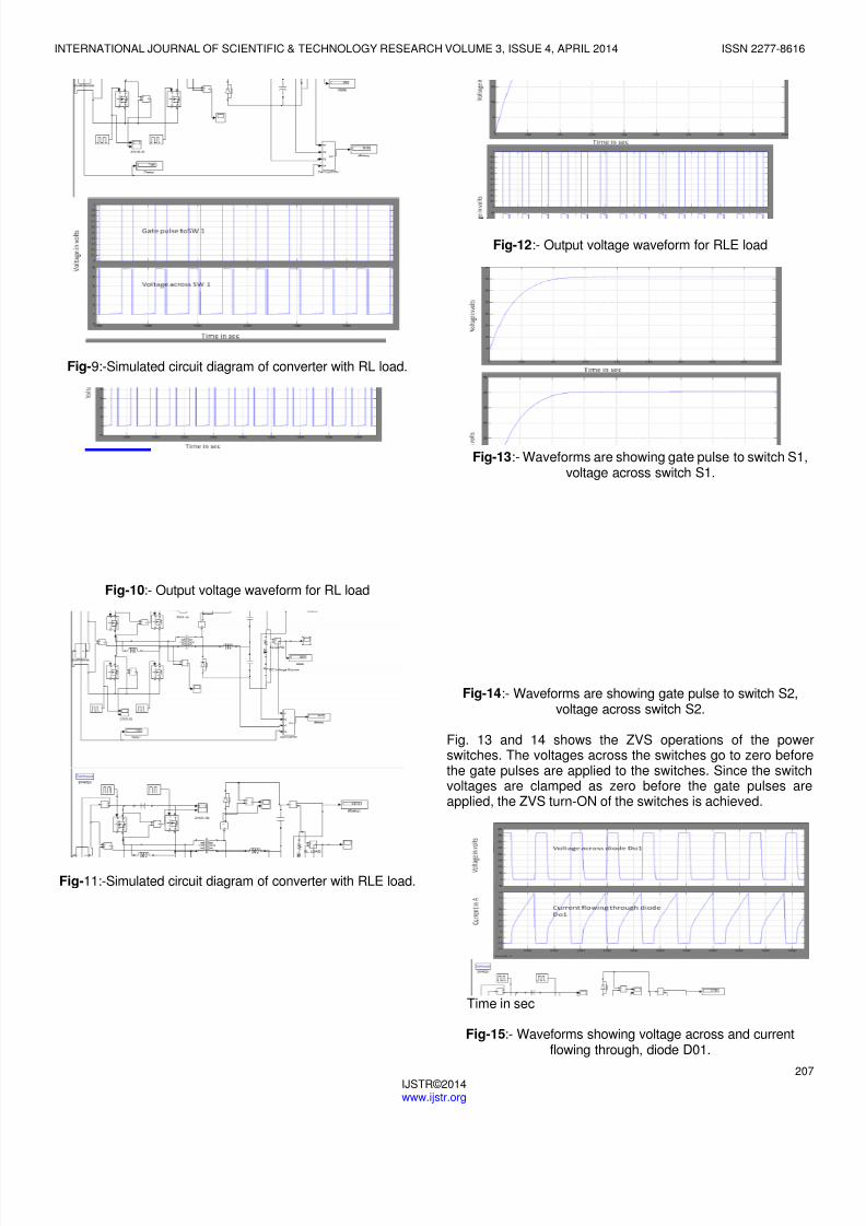
Fig-12:- Output voltage waveform for RLE load
Fig-13:- Waveforms are showing gate pulse to switch S1,voltage across switch S1.
Fig-14:- Waveforms are showing gate pulse to switch S2,voltage across switch S2.
Fig. 13 and 14 shows the ZVS operations of the poweswitches. The voltages across the switches go to zero beforethe gate pulses are applied to the switches. Since the switchvoltages are clamped as zero before the gate pulses areapplied, the ZVS turn-ON of the switches is achieved.
Time in sec
Fig-15:- Waveforms showing voltage across and currentflowing through, diode D01.

8/11/2019 A Zvzcs Full Bridge Converter With High Voltage Gain by Solar Energy Source
http://slidepdf.com/reader/full/a-zvzcs-full-bridge-converter-with-high-voltage-gain-by-solar-energy-source 6/7
INTERNATIONAL JOURNAL OF SCIENTIFIC & TECHNOLOGY RESEARCH VOLUME 3, ISSUE 4, APRIL 2014 ISSN 2277-8616
208IJSTR©2014www.ijstr.org
Fig. 15 shows ZCS of the output diodes. After the diodecurrents fall to zero, the voltages across the diode rise to theoutput voltage Vo. Therefore, the ZCS turn-OFF of the outputdiodes is achieved.
LOAD VOLTAGE EFFICIENCY ZVS ZCS
RLOAD
RLLOAD
RLELOAD
368.8V
354V
356V
95.91%
88.26%
84.03%
Achieved
Achieved
Achieved
Achieved
Achieved
Achieved
Fig 16:-Comparison table
Fig16 shows the comparison table of different loads.Here R load has the highest efficiency and for allloads(R, RL, RLE)-ZVS and ZCS are achieved.
5. CONCLUSIONIn this paper, the zvzcs asymmetrical full bridge converterwith high voltage gain is interfaced with a PV module. Theconverter is able to provide a high efficiency and high-voltagegain with relatively low transformer turns ratio. The ZVS of allpower switches and ZCS of the output diodes are achieved.Therefore, the converter is suitable for high-voltageapplications. In this paper, both dc and solar energy sourcesare used as input source. And from both the result highvoltage gain and high efficiency is obtained. So in this highlyenergy concerned world effective utilization of solar energywith this concept of converter can be used for manyapplications. Also from this paper performance of differenttypes of loads are studied and from that we obtained theconclusion that R load has the highest efficiency and for allloads(R, RL, RLE)-ZVS and ZCS are achieved.
6. REFERENCES
[1]. R. J. Wai, W. H. Wang, and C. Y. Lin, ―High -performance stand-alone photovoltaic generationsystem,‖ IEEE Trans. Ind. Electron., vol. 55, no. 1,pp. 240 –250, Jan. 2008.
[2]. C. Wang and M. H. Nehrir, ―Power management of astandalone wind/photovoltaic/fuel cell energysystem,‖ IEEE Trans. Energy Convers., vol. 23, no.3, pp. 957 –967, Sep. 2008.
[3]. R. J. Wai and W. H. Wang, ―Grid-connectedphotovoltaic generation system,‖ IEEETrans.CircuitsSyst. I, Reg. Papers, vol. 55, no. 3, pp. 953 –964, Apr. 2008.
[4]. M. Prudente, L. L. Pfitscher, G. Emmendoerfer, E. F.Romaneli, and R. Fules, ―Voltage multiplier cellsapplied to non-isolated DC-DC converters,‖ IEEE
Trans. Power Electron., vol. 23, no. 2, pp. 871 –887Mar. 2008.
[5]. E. H. Ismail, M. A. Al-Saffar, A. J. Sabzali, and A. AFardoun, ―A family of single-switch PWM converterswith high step-up conversion ratio,‖ IEEE TransCircuit Syst. I, vol. 55, no. 4, pp. 1159 –1171, May2008.
[6]. W.-S. Liu, J.-F. Chen, T.-J. Liang, and R.-L. Lin―Multicascoded sources for a high-efficiency fuel-celhybrid power system in high-voltage. application,IEEE Trans. Power Electron., vol. 26, no. 3, pp. 931 –942, Mar.
[7]. Z. Liang, R. Guo, J. Li, and A. Q. Huang, ―A highefficiency PV modal integrated DC/DC converter foPV energy harvest in FREEDM systems,‖ IEEETrans. Power Electron., vol. 26, no. 3, pp. 897 –909Mar. 2011
[8]. L. Zhu, K. Wang, F. C. Lee, and J. S. Lai, ―New start
up schemes for isolated full-bridge boost converters,IEEE Trans. Power Electron., vol. 18, no. 4, pp. 946 –951, Jul. 2003
[9]. Q. Zhao, F. Tao, Y. Hu, and F. C. Lee, ―Active -clampDC/DC converter using magnetic switches,‖ in ProcIEEE Appl. Power Electron. Conf.Expo., 2001, pp946 –952.
[10]. D. A. Grant, Y. Darroman, and J. Suter, ―Synthesis otapped-inductor switched-mode converters,‖ IEEETrans. Power Electron., vol. 22, no. 5, pp. 1964 –1969, Sep. 2007.
[11].
L.-S. Yang, T.-J. Liang, and J.-F. Chen―Transformerless DC-DC converters with high stepup voltage gain,‖ IEEE Trans. Ind. Electron., vol. 56no. 8, pp. 3144 –3152, Aug. 2009
[12]. E. Adib and H. Farzanehfard, ―Zero-voltage transitioncurrent-fed full bridge PWM converter,‖ IEEE TransPower Electron., vol. 24, no. 4, pp. 1041 –1047, Apr2009.
[13]. Y. Jang and M. M. Jovanovic, ―A new family of fullbridge ZVS converters,‖ IEEE Trans. PoweElectron., vol. 19, no. 3, pp. 701 –708, May 2004.
[14].
M. Borage, S. Tiwari, S. Bhardwaj, and S. Kotaiah, ―Afull-bridge DC-DC converter with zero-voltageswitching over the entire conversion range,‖ IEEETrans. Power Electron., vol. 23, no. 4, pp. 1743 –1750, Jul. 2008.
[15]. Y. Jang and M. M. Jovanovic, ―A new PWM ZVS fullbridge ZVS converter,‖ IEEE Trans. Power Electron.vol. 22, no. 3, pp. 987 –994, May 2007.
[16]. A. Fiedler and H. Grotstollen, ―Investigation oasymmetrical phase shifted full bridge,‖ in Proc. IEEEIECON, 1995, pp. 434 –439.

8/11/2019 A Zvzcs Full Bridge Converter With High Voltage Gain by Solar Energy Source
http://slidepdf.com/reader/full/a-zvzcs-full-bridge-converter-with-high-voltage-gain-by-solar-energy-source 7/7
INTERNATIONAL JOURNAL OF SCIENTIFIC & TECHNOLOGY RESEARCH VOLUME 3, ISSUE 4, APRIL 2014 ISSN 2277-8616
209IJSTR©2014ij
[17]. A. J. Zhang, G. Huang, and Y. Gu, ―Asymmetrical fullbridge DC-to-DC converter,‖ U.S. Patent 6 466 458,Oct. 15, 2002
[18]. S.Chowdhury, S.P.Chowdhury, G.A.Taylor, andY.H.Song,―Mathematical Modeling and PerformanceEvaluation of a Stand-Alone Polycrystalline PV Plant
with MPPT Facility,‖ IEEE Power and Energy SocietyGeneral Meeting - Conversion and Delivery ofElectrical Energy in the 21st Century, July 20-24,2008, Pittsburg, USA.
[19]. Jee-Hoon Jung, and S. Ahmed, ―Model Constructionof Single Crystalline Photovoltaic Panels for Real-time Simulation,‖ IEEE Energy Conversion Congress& Expo, September 12-16, 2010, Atlanta, USA.
[20]. S. Nema, R.K.Nema, and G.Agnihotri, ―Matlab /simulink based study of photovoltaic cells / modules /array and their experimental verification,‖International Journal of Energy and Environment,
pp.487-500.500, Volume 1, Issue 3, 2010.
[21]. Hyun-Lark Do, ―Asymmetrical Full-bridge Converterwith High-Voltage Gain‖ IEEE Trans. Power Electron,vol. 27, no. 2, February 2012.