department of defense test method standard
TRANSCRIPT

i
INCH–POUND MIL–STD–750–2 w/CHANGE 2 23 NOVEMBER 2012 SUPERSEDING MIL–STD–750-2 w/CHANGE 1 25 June 2012 (see 6.4)
DEPARTMENT OF DEFENSE
TEST METHOD STANDARD
MECHANICAL TEST METHODS FOR SEMICONDUCTOR DEVICES
PART 2: TEST METHODS 2001 THROUGH 2999
AMSC N/A FSC 5961
The documentation and process conversion measures necessary to comply with this revision shall be completed by 23-FEBRUARY-2013.

MIL-STD-750-2 w/CHANGE 2
ii
FOREWORD
1. This standard is approved for use by all Departments and Agencies of the Department of Defense. 2. This revision has resulted in many changes to the format, but the most significant one is the splitting the
document into parts. See MIL–STD–750 for the change summary. 3. Comments, suggestions, or questions on this document should be addressed to: Commander, Defense
Logistics Agency, DLA Land and Maritime, ATTN: VAC, P.O. Box 3990, Columbus, OH 43218–3990, or emailed to [email protected]. Since contact information can change, you may want to verify the currency of this address information using the ASSIST Online database at https://assist.dla.mil.

MIL-STD-750-2 w/CHANGE 2
iii
SUMMARY OF CHANGE 2 MODIFICATIONS
1. Test method 2038, “Surface Mount End Cap Bond Integrity”, was added. The purpose of this method is to
simulate the stresses imposed on surface mount devices during installation, removal, and rework.
2. The following modification to MIL-STD-750-2 has been made:
Test Method Modification 2038 New Method

MIL-STD-750-2 w/CHANGE 2
iv
PARAGRAPH PAGE FOREWORD…………………………………………………………………………………………………..……...ii SUMMARY OF CHANGE 2 MODIFICATIONS…………………………………………………………………..iii
1. SCOPE ..................................................................................................................................... 1 1.1 Purpose ............................................................................................................................... 1 1.2 Numbering system .............................................................................................................. 1 1.2.1 Classification of tests ..................................................................................................... 1 1.2.2 Test method revisions ................................................................................................... 1 1.3 Methods of reference .......................................................................................................... 1 2. APPLICABLE DOCUMENTS .................................................................................................... 2 2.1 General ............................................................................................................................... 2 2.2 Government documents ...................................................................................................... 2 2.2.1 Specifications, standards, and handbooks .................................................................... 2 2.3 Non-Government publications ............................................................................................. 2 2.4 Order of precedence ........................................................................................................... 3 3. DEFINITIONS ........................................................................................................................... 4 3.1 Acronyms, symbols, and definitions .................................................................................... 4 3.2 Acronyms used in this standard .......................................................................................... 4 4. GENERAL REQUIREMENTS ................................................................................................... 4 4.1 General ............................................................................................................................... 4 4.2 Test circuits ......................................................................................................................... 5 4.3 Destructive tests .................................................................................................................. 5 4.4 Non–destructive tests .......................................................................................................... 6 4.5 Laboratory suitability ........................................................................................................... 6 5. DETAILED REQUIREMENTS ................................................................................................... 6 6. NOTES ..................................................................................................................................... 6 6.1 Intended use ....................................................................................................................... 6 6.2 International standardization agreement ............................................................................. 7 6.3 Subject term (key word) listing ............................................................................................ 7 6.4 Supersession data............................................................................................................... 7 6.5 Change notations ................................................................................................................ 7

MIL-STD-750-2 w/CHANGE 2
v
CONTENTS
FIGURE TITLE
2017–1 Uniform force distribution 2017–2 Rotational capability 2017–3 Perpendicular force application 2017–4 Die shear strength criteria 2037–1 Minimum bond pull limits 2037–2 Wire loop angle 2037–3 Flat loop wire pull testing 2038–1 Sample apparatus fixture with force measuring gauge 2038–2 Close up view of sample apparatus fixture 2038–3 Condition B 2038–4 Condition C 2038–5 Condition D 2052–1 Typical STU 2069–1 Bond dimensions 2069–2 Torn bonds 2069–3 Acceptable and unacceptable voids and excessive pigtails 2069–4 Acceptable and unacceptable bonding material build-up 2069–5 Extraneous bonding material build-up 2069–6 Acceptable and unacceptable excess material 2070–1 Metallization scratches and voids (expanded contact) 2070–2 Cracks and chips 2070–3 Bond dimensions 2070–4 Lifted or torn bonds 2070–5 Mesh geometry 2070–6 Interdigitated geometry 2070–7 Spine geometry 2071–1 Radial cracks extending more than one-half the distance from pin to outer member 2071–2 Circumferential cracks 2071–3 Bubbles in glass exceeding one-third of the sealing area 2071–4 Single bubble or void 2071–5 Two bubbles in a line 2071–6 Interconnecting bubbles 2071–7 Meniscus cracks 2071–8 Chip outs 2071–9 Transparent glass diode 2071–10 Braze separation/delamination 2071–11 Crack in braze metallization 2071–12 Discontinuous braze metallization 2071–13 Ceramic feedthrough visual inspection criteria 2071–14 Rejectable foreign material conditions 2072–1 Metallization scratches, probe marks and voids 2072–2 Innermost guard band metallization scratches, probe marks and voids 2072–3 Active region metallization scratches, probe marks and voids 2072–4 Pad and contact metallization scratches, probe marks and voids 2072–5 Contact metallization scratches, probe marks and voids 2072–6 Metallization probing damage 2072–7 Metallization bridging between two normally unconnected metallization areas 2072–8 Metallization bridging between two normally unconnected metallization paths 2072–9 Metallization misalignment, cross section view 2072–10 Metallization misalignment 2072–11 Passivation and diffusion faults 2072–12 Passivation and diffusion faults, cross section view
*

MIL-STD-750-2 w/CHANGE 2
vi
CONTENTS
FIGURE TITLE 2072–13 Passivation and diffusion faults 2072–14 Contact window in a diffused area which extends across a junction faults 2072–15 Die cracks and chips 2072–16 Bond dimensions 2072–17 Lift and torn bonds 2072–18 Ball bond diameter is less than 2 times or greater than 5 times the wire diameter 2072–19 Ball bonds where the wire exit is not completely within the periphery of the ball 2072–20 Ball bonds where exiting wire is not within boundaries of the bonding pad 2072–21 Intermetallic formation at the periphery of gold ball bond 2072–22 Wedge bonds on the die or package post criteria 2072–23 Tailless bond dimensions 2072–24 Wire bond to bonding pad area misalignment 2072–25 Wire bond tails contacting with metallization not covered by glassivation 2072–26 Wire bond tails limits 2072–27 Bonds on the flat surface of the post top 2072–28 A bond on top of another bond 2072–29 Bond to unglassivated die metallization 2072–30 Bond to glassivated die metallization 2072–31 Adjacent bonds violating separation limits 2072–32 Wire that violates allowed limits 2072–33 Wire nicks, tears, bonds, cuts, crimps, scoring, or neckdown 2072–34 Bond tearing at interface of pad and wire 2072–35 Wire that has no arc or stress relief 2072–36 Wire not within 10 degrees of the perpendicular to the surface of the chip 2072–37 Excessive lead burn at lead post weld 2072–38 Pigtail to unglassivated active metal spacing 2072–39 Bow or loop in wire between double bonds at post 2072–40 Excessive loops, bows, or sags in wire 2072–41 Non-embedded foreign particles present on the surface of the die 2072–42 Glass-embedded foreign particles on the die that bridge paths or junctions 2072–43 Ink on the surface of the die 2072–44 Balling of the die mounting material 2072–45 Tipped or tilted die 2072–46 Acceptable and unacceptable voids and excessive pigtails 2072–47 Acceptable and unacceptable bonding material build–up 2072–48 Extraneous bonding material build–up 2072–49 Acceptable and unacceptable excess material 2072–50 Unacceptable die placement 2072–51 Two or more adjacent active metallization paths not covered by glassivation 2072–52 Unglassivated areas at the edge of bonding pad that expose silicon 2072–53 Glassivation covering the design bonding pad area 2073–1 Button contact diodes 2073–2 High voltage planar diode I 2073–3 High voltage planar diodes II 2073–4 Inside moat mesa diodes 2073–5 Low voltage contact overlay diodes 2073–6 Low voltage planar diode 2073–7 Outside moat mesa diodes 2073–8 Schottky barrier diodes 2074–1 Die chip outs 2074–2 Die cracks 2074–A1 Glass cracks and chips 2074–A2 Package deformities
MIL-STD-750-2 w/CHANGE 2
vii
CONTENTS
FIGURE TITLE 2074–A3 Solder protrusions 2074–A4 Embedded whisker 2074–A5 Whisker toe contact 2074–A6 Whisker toe contact on top surface of die 2074–A7 Whisker heel contact 2074–A8 Whisker point contact 2074–A9 S bend whisker compressed height 2074–A10 C bend whisker compressed height 2074–A11 Die alignment 2074–B1 Straight through internal construction 2074–B2 Solder voids 2074–B3 Solder bridge 2074–B4 Solder voids 2074–B5 Solder overflow 2074–B6 Solder slivers and spikes 2074–B7 Die-to-die solder connection 2074–C1 Glass cracks 2074–C2 High seal 2074–C3 Insufficient seal 2074–C4 Plug alignment 2074–C5 Plug displacement 2074–C6 Incomplete weld 2074–D1 Chip outs 2074–D2 Deformity 2074–D3 Positioning 2074–D4 Insufficient seal 2074–D5 Tilt 2074–D6 Die non-contract 2074–D7 Plug offset 2074–D8 Plug tilt angle 2074–D9 Lead offset 2074–D10 End-cap clearance 2074–D11 End-cap tilt 2074–D12 End-cap deformation 2074–D13 End-cap rotation 2074–D14 Mounting surface nicks and pits 2074–E1 Whisker touches glass body wall 2074–E2 Whisker loops touch one another 2074–E3 Whisker angle over 10 degrees from normal 2074–E4 Die touches glass package 2074–G1 Solder protrusion 2074–G2 Solder flow 2074–G3 Element alignment 2074–G4 Element tilt 2074–G5 Die chip out 2074–G6 Die cracks 2074–H1 Offset die 2074–H2 Tilted die 2074–I1 Diamond base construction 2076–1 Acceptable and unacceptable voids and excessive pigtails 2076–2 Lid seal voids and rejection criterion (drawing) 2076–3 Clearance in dual-in-line or flat pack type device 2076–4 Clearance in round or box transistor type device
MIL-STD-750-2 w/CHANGE 2
viii
CONTENTS
FIGURE TITLE 2076–5 Clearance in cylindrical axial lead type device 2076–6 Typical digital radiography view of a UB device 2077–1 Cross-sectional planes at various passivation steps 2077–2 Directional edge 2077–3 Viewing angle 2077–4 Wafer sampling procedures 2077–5 Concept of reduction of cross sectional area of metallization as accept/reject criteria 2077–6 Void near oxide step at 3,400X 2077–7 Voids at oxide step at 3,300X 2077–8 Tunnel/cave at oxide step at 10,000X 2077–9 Tunnel/cave at oxide step at 5,000X 2077–10 Separation of metallization at oxide step at base contact at 10,000X 2077–11 Separation of metallization at contact step at 7,000X 2077–12 Crack-like defect at oxide step at 20,000X 2077–13 Crack-like defect at oxide step at 7,000X 2077–14 Acceptable thinning at oxide step (multi-level-metal) at 7,200X 2077–15 Unacceptable thinning at oxide step (multi-level-metal) at 7,200X 2077–16 Steep oxide step (MOS) at 6,000X 2077–17 Steep oxide step (MOS) at 9,500X 2077–18 Peeling or lifting of general metallization in contact window area at 5,000X 2077–19 General metallization voids at 10,000X 2077–20 General metallization voids at 5,000X (reject) 2077–21 Etch back/undercut type of notch at oxide step (multi-layered-metal) at 5,000X 2077–22 Barrier or adhesion layer etch back/undercut type of notch at oxide step (multi-layered-metal) at 5,000X 2078–1 Metallization scratches and voids 2078–2 Metallization scratches and voids – Continued 2078–3 Passivation and diffusion faults 2078–4 Cracks and chips 2078–5 Cracks and chips (continued) 2078–6 Bond dimensions, wedge 2078–7 Bond dimensions, tailless or crescent 2078–8 Pigtail length 2078–9 Unacceptable wirebond neckdown 2078–10 Wire bond stress relief 2078–11 Wirebond to pad placement 2078–12 Extraneous bonding material build-up 2078–13 Acceptable and unacceptable excess material 2100–1 Typical scan location on flat surface mounted devices 2100–2 Scan locations on can style package 2100–3 Scan locations on metal base flange mount style package 2100–4 Scan locations on glass, axial leaded package style 2100–5 Scan locations – ceramic, metal sealed, single in-line package 2100–6 Scan locations on metal electrode face (MELF) style package 2101–1 Axial lead or surface mount construction 2101–2 Axial lead or surface mount construction 2101–3 Stud package

MIL-STD-750-2 w/CHANGE 2
ix
CONTENTS
TABLE TITLE
I Destructive tests II Non-destructive tests 2031–I Test conditions 2037–I Minimum bond strength 2052–I Package height vs. test frequency for 20 g acceleration (condition A) 2070–I GaAs microwave device high magnification requirements 2070–II Resistor criteria 2072–I Die magnification requirements 2073–I Magnification requirements 2077–I Wafer sampling procedures 2077–II Examination procedure for sample dice 2078–I Die magnification requirements 2101–I Mandatory procedures 2101–II Die attach criteria
TEST METHOD NO. TITLE
2005.2 Axial lead tensile test 2006 Constant acceleration 2016.2 Shock 2017.3 Die attach integrity 2026.11 Solderability 2031.4 Resistance to soldering heat 2036.5 Terminal strength 2037.1 Bond strength (destructive bond pull test) 2038 Surface mount end cap bond integrity 2046.2 Vibration fatigue 2051.1 Vibration noise 2052.5 Particle impact noise detection (PIND) test 2056 Vibration, variable frequency 2057.2 Vibration, variable frequency (monitored) 2066 Physical dimensions 2068 External visual for nontransparent glass–encased, double plug, noncavity axial
leaded diodes 2069.2 Pre–cap visual, power MOSFET's 2070.2 Pre–cap visual microwave discrete and multichip transistors 2071.7 Visual and mechanical examination 2072.7 Internal visual transistor (pre–cap) inspection 2073.2 Visual inspection for die (semiconductor diode) 2074.6 Internal visual inspection (discrete semiconductor diodes) 2075.1 Decap internal visual design verification 2076.4 Radiography 2077.4 Scanning electron microscope inspection of metallization 2078 Internal visual for wire bonded diodes/rectifiers 2081 Forward instability, shock (FIST) 2082 Backward instability, vibration (BIST) 2100 X–ray fluorescence (XRF) scan locations for discrete semiconductor Tin – Lead
content analysis 2101.3 Destructive physical analysis for diodes 2102.1 Destructive physical analysis for wire bonded devices 2103 Design verification for surface mount devices
*

MIL-STD-750-2 w/CHANGE 2
1
1. SCOPE
1.1 Purpose. Part 2 of this test method standard establishes uniform test methods for the mechanical testing to determine resistance to deleterious effects of natural elements and conditions surrounding military operations. For the purpose of this standard, the term "devices" includes such items as transistors, diodes, voltage regulators, rectifiers, tunnel diodes, and other related parts. This part of a multipart test method standard is intended to apply only to semiconductor devices.
1.2 Numbering system. The test methods are designated by numbers assigned in accordance with the following system.
1.2.1 Classification of tests. The mechanical test methods included in this part of a multipart test method standard are numbered 2005 to 2103 inclusive.
1.2.2 Test method revisions. Revisions are numbered consecutively using a period to separate the test method number and the revision number. For example, 2005.2 is the second revision of test method 2005.
1.3 Method of reference. When applicable, test methods contained herein shall be referenced in the individual specification or specification sheet by specifying the test method number and, the details required in the summary of the applicable test method shall be listed. To avoid the necessity for changing documents that refer to test methods of this standard, the revision number should not be used when referencing test methods. (For example: Use 2005 versus 2005.2.)

MIL-STD-750-2 w/CHANGE 2
2
2. APPLICABLE DOCUMENTS
2.1 General. The documents listed in this section are specified in sections 3, 4, 5, and the individual test methods of this standard. This section does not include documents cited in other sections of this standard or recommended for additional information or as examples. While every effort has been made to ensure the completeness of this list, document users are cautioned that they must meet all specified requirements documents cited in sections 3, 4, 5, and the individual test methods of this standard, whether or not they are listed.
2.2 Government documents.
2.2.1 Specifications, standards, and handbooks. The following specifications, standards, and handbooks form a part of this document to the extent specified herein. Unless otherwise specified, the issues of these documents are those cited in the solicitation or contract.
DEPARTMENT OF DEFENSE SPECIFICATIONS
MIL–PRF–19500 – Semiconductor Devices, General Specification for.
DEPARTMENT OF DEFENSE STANDARDS
MIL–STD–750 – Test Methods For Semiconductor Devices. MIL–STD–750–1 – Environmental Test Methods For Semiconductor Devices. MIL–STD–750–3 – Electrical Test Methods For Semiconductor Devices. MIL–STD–883 – Test Method Standard Microcircuits.
FEDERAL STANDARDS
FED–STD–595 – Colors used in Government Procurement. FED–STD–595/15102–15123 – Blue, Gloss. FED–STD–595/25102–25109 – Blue, Semi-gloss.
(Copies of these documents are available online at https://assist.dla.mil/quicksearch or https://assist.dla.mil or from
the Standardization Document Order Desk, 700 Robbins Avenue, Building 4D, Philadelphia, PA 19111-5094.)
2.3 Non-Government publications. The following documents form a part of this document to the extent specified herein. Unless otherwise specified, the issues of these documents are those cited in the solicitation or contract.
ASME INTERNATIONAL (ASME)
ASME Y14.38 – Abbreviations and Acronyms for Use on Drawings and Related Documents.
(Copies of these documents are available online at http://www.asme.org or from ASME International, Three Park Avenue, New York, NY 10016–5990.)

MIL-STD-750-2 w/CHANGE 2
3
ASTM INTERNATIONAL (ASTM)
ASTM D1867 – Standard Specification for Copper-Clad Thermosetting Laminates for Printed Wiring.
(Copies of these documents are available online at http://www.astm.org or from ASTM International, 100 Barr
Harbor Drive, P.O. Box C700, West Conshohocken, PA 19428–2959.)
INTERNATIONAL ORGANIZATION FOR STANDARDIZATION (ISO)
ISO 14644–1 – Cleanrooms and Associated Controlled Environments – Part 1: Classification of Air Cleanliness.
ISO 14644–2 – Cleanrooms and Associated Controlled Environments – Part 2: Specifications for Testing and Monitoring to Prove Continued Compliance with ISO 14644–1.
(Copies of these documents are available online at http://www.iso.ch or from the International Organization for
Standardization American National Standards Institute, 11 West 42nd Street, 13th Floor, New York, NY 10036.)
IPC – ASSOCIATION CONNECTING ELECTRONICS INDUSTRIES (IPC)
IPC J–STD–002 – Solderability Tests for Component Leads, Terminations, Lugs, Terminals and Wires.
IPC J–STD–004 – Requirements for Soldering Fluxes. IPC J–STD–005 – Requirements for Soldering Pastes. IPC J–STD–006 – Requirements for Electronic Grade Solder Alloys and Fluxed and Non-fluxed Solid
Solders for Electronic Soldering Applications. IPC–9701 – Performance Test Methods and Qualification Requirements for Surface Mount
Solder Attachments.
(Copies of these documents are available online at http://www.ipc.org or from IPC – Association Connecting Electronics Industries, 3000 Lakeside Drive, Suite 309 S, Bannockburn, IL 60015–1249.)
JEDEC – SOLID STATE TECHNOLOGY ASSOCIATION (JEDEC) JEDEC JESD213 – Common Test Method for Detecting Component Surface Finish Materials.
(Copies of this document are available online at http://www.jedec.org or from JEDEC, 3103 North 10th Street, Suite
240-S Arlington, VA 22201–2107.)
NCSL INTERNATIONAL (NCSL)
NCSL Z540.3 – Requirements for the Calibration of Measuring and Test Equipment.
(Copies of this document are available online at http://www.ncsli.org or can be obtained through NCSL International, 2995 Wilderness Place, Suite 107, Boulder, CO 80301–5404.)
2.4 Order of precedence. Unless otherwise noted herein or in the contract, in the event of a conflict between the text of this document and the references cited herein (except for related applicable specification sheet, the text of this document takes precedence. Nothing in this document, however, supersedes applicable laws and regulations unless a specific exemption has been obtained.

MIL-STD-750-2 w/CHANGE 2
4
3. DEFINITIONS
3.1 Acronyms, symbols, and definitions. For the purposes of this test method standard, the acronyms, symbols, and definitions specified in MIL–PRF–19500, ASME Y14.38, and herein shall apply.
3.2 Acronyms used in this standard. Acronyms used in this test method standard are defined as follows:
a. BIST – Backward instability shock test. b. dB – Decibel. c. DPA – Destructive physical analysis. d. DUT – Device under test. e. FET – Field-effect transistor. f. FIST – Forward instability shock test. g. GaAs – Gallium Arsenide. h. Hz – Hertz. i. mA – Milliamps j. mV – Milivolts. k. MOSFET – Metal oxide semiconductor field-effect transistor. l. NIST – National Institute of Standards and Technology. m. PIND – Particle impact noise detection. n. RF – Radio frequency. o. rms – Root means square. p. SEM – Scanning electron microscope. q. STU – Sensitivity test unit. r. UHF – Ultra high frequency. s. VPR – Vapor phase reflow.
4. GENERAL REQUIREMENTS
4.1 General. Unless otherwise specified in the individual test method, the general requirements of MIL–STD–750
shall apply.

MIL-STD-750-2 w/CHANGE 2
5
4.2 Test circuits. The test circuits shown in the test methods of this test method standard are given as examples
which may be used for the measurements. They are not necessarily the only test circuits which can be used; however the manufacturer shall demonstrate to the Government that other test circuits which they may desire to use will give results within the desired accuracy of measurement. Circuits are shown for PNP transistors in one circuit configuration only. They may readily be adapted for NPN devices and for other circuit configurations.
4.3 Destructive tests. Unless otherwise demonstrated, the test methods listed in table I shall be classified as destructive. MIL–STD–750 covers the necessary actions needed to reclassify a test method as non-destructive.
TABLE I. Destructive tests.
Test method number Test
2017 Die shear test
2031 Soldering heat
2036 Terminal strength
2037 Post-seal bond strength
207538 Surface mount end cap bond integrity
2075 Decap internal visual design verification
2077 SEM
All other mechanical tests (other than those listed in 4.4) shall be considered destructive initially, but may subsequently be considered non-destructive upon accumulation of sufficient data to indicate that the test is non-destructive. The accumulation of data from five repetitions of the specified test on the same sample of product, without significant evidence of cumulative degradation in any device in the sample, is considered sufficient evidence that the test is non-destructive for the device of that manufacturer. Any test specified as a 100-percent screen shall be considered non-destructive for the stress level and duration or number of cycles applied as a screen.

MIL-STD-750-2 w/CHANGE 2
6
4.4 Non–destructive tests. Unless otherwise demonstrated, the test methods listed in table II shall be classified as
nondestructive.
TABLE II. Non-destructive tests.
Test method number Test
2006 Constant acceleration
2016 Shock
2026 Solderability (if the original lead finish is unchanged and if the maximum allowable number of reworks is not exceeded.)
2052 PIND test
2056 Vibration, variable frequency
2066 Physical dimensions
2069, 2070, 2072, 2073, 2074 Internal visual (pre-cap)
2071 External visual
2076 Radiographic inspection
2081 FIST
2082 BIST
NOTE: When the junction temperature exceeds the device maximum rated junction temperature for any operation or test (including electrical stress test), these tests shall be considered destructive except under transient surge or nonrepetitive fault conditions, or approved accelerated screening, when it may be desirable to allow the junction temperature to exceed the rated junction temperature. The feasibility shall be determined on a part by part basis and, in the case where it is allowed adequate sample testing, shall be performed to provide the proper reliability safeguards.
4.5 Laboratory suitability. Prior to processing any semiconductor devices intended for use in any military system or sub-system, the facility performing the test(s) shall be audited by the DLA Land and Maritime, Sourcing and Qualification Division and be granted written laboratory suitability status for each test method to be employed. Processing of any devices by any facility without laboratory suitability status for the test methods used shall render the processed devices nonconforming.
5. DETAILED REQUIREMENTS
This section is not applicable to this standard.
6. NOTES
(This section contains information of a general or explanatory nature that may be helpful, but is not mandatory.)
6.1 Intended use. The intended use of this test method standard is to establish appropriate conditions for testing semiconductor devices to give test results that simulate the actual service conditions existing in the field. This test method standard has been prepared to provide uniform test methods, controls, and procedures for determining with predictability the suitability of such devices within military, aerospace and special application equipment.

MIL-STD-750-2 w/CHANGE 2
7
6.2 International standardization agreement. Certain provisions of this test method standard are the subject of international standardization agreement. When amendment, revision, or cancellation of this test method standard is proposed which will affect or violate the international agreement concerned, the preparing activity will take appropriate reconciliation action through international standardization channels, including departmental standardization offices, if required.
6.3 Subject term (key word) listing.
Destructive tests Laboratory suitability Mechanical characteristics tests Non–destructive tests
6.4 Supersession data. The main body and five parts (–1 through –5) of this revision of MIL–STD–750 replace
superseded MIL–STD–750E.
6.5 Change notations. The margins of this standard are marked with asterisks to indicate modifications generated by this change. This was done as a convenience only and the Government assumes no liability whatsoever for any inaccuracies in these notations. Bidders and contractors are cautioned to evaluate the requirements of this document based on the entire content irrespective of the marginal notations.
*

MIL-STD-750-2 w/CHANGE 2
METHOD 2005.2 1 of 1
METHOD 2005.2
AXIAL LEAD TENSILE TEST
1. Purpose. The purpose of this test method is to establish the capability of axial lead glass body diodes to be free of intermittents or opens when measured in the forward mode under conditions of tensile stress and controlled temperature. This test may be destructive.
2. Apparatus.
a. Digital volt meter and constant current source capable of supplying 100 mA of dc current to the DUT. A battery supply is preferred but if a constant current supply is used, a voltage clamp of approximately five volts shall be used.
b. Load cell with 10 pounds (4.56 Kg) full scale dial (or equivalent) capable of measuring 8 pounds
(3.63 Kg) ±10 percent. c. Pull test fixture capable of clamping both ends of the diode while applying an 8 pound (3.63 Kg) axial pull.
One clamp must be electrically isolated allowing the diode forward voltage to be monitored. d. Hot air supply capable of heating the diode ambient to TA = +150°C ±5°C.
(TJ approximately +175°C)
3. Procedure. The diode under test shall be mounted in the pull test fixture. The electrical monitoring equipment shall be connected to the diode leads. A forward current of 100 mA is passed through the diode while noting the forward voltage. The ambient temperature of the diode is then increased to +150°C ±5°C. NOTE: The diode junction temperature (TJ) will be approximately +25°C higher than ambient (TJ approximately +175°C) due to the thermal resistance of the diode when testing small (computer) diodes at 100 mA dc in the forward direction. A silicon diode (computer type) also has an approximate negative 1.2 mV/°C temperature coefficient at 100 mA. Therefore a 150 mV decline (100 mV minimum) in voltage should be expected during the ambient temperature increase (from +25°C to +150°C). After stabilizing at this temperature, then the axial lead pull force of eight pounds shall be applied while observing the forward voltage change.
4. Criteria for rejection. An acceptable device shall not exhibit a forward voltage increase of more than 30 mV during the 8 pound pull. Any instability or open is cause for rejection.
5. Summary. The following conditions shall be specified in the applicable performance specification sheet or acquisition document:
a. Ambient test temperature, if other than +150°C ±5°C. b. Measurement current, if other than 100 mA dc. c. Axial tensile stress, if other than 8 pounds (3.63 Kg). d. Allowable change in forward voltage, if other than 30 mV.

MIL-STD-750-2 w/CHANGE 2
This page is intentionally left blank.

MIL-STD-750-2 w/CHANGE 2
METHOD 2006 1 of 1
METHOD 2006
CONSTANT ACCELERATION
1. Purpose. The constant acceleration test is used to determine the effect on semiconductor devices of a centrifugal force. This test is an accelerated test designed to indicate types of structural and mechanical weaknesses not necessarily detected in shock and vibration tests.
2. Apparatus. Constant acceleration tests shall be made on an apparatus capable of meeting the minimum requirements of the individual specification sheets.
3. Procedure. The device shall be restrained by its case, or by normal mountings, and the leads or cables secured. A centrifugal acceleration of the value specified shall then be applied to the device for one minute in each of the orientations X1, X2, Y1, Y2, Z1, and Z2. The acceleration shall be increased gradually, to the value specified, in not less than 20 seconds. The acceleration shall be decreased gradually to zero in not less than 20 seconds.
4. Summary. The following conditions shall be specified in the applicable performance specification sheet or acquisition document:
a. Amount of centrifugal force to be applied, in gravity units (g) (see 3). b. Measurements to be made after test.

MIL-STD-750-2 w/CHANGE 2
This page is intentionally left blank.

MIL-STD-750-2 w/CHANGE 2
METHOD 2016.2 1 of 1
METHOD 2016.2
SHOCK
1. Purpose. This test method is intended to determine the ability of the semiconductor devices to withstand moderately severe shocks such as would be produced by rough handling, transportation, or field operation. Shocks of this type may disturb operating characteristics or cause damage similar to that resulting from excessive vibration, particularly if the shock pulses are repetitive.
2. Apparatus. The shock testing apparatus shall be capable of providing shock pulses of the specified peak acceleration and pulse duration to the body of the device. The acceleration pulse, as determined from the output of a transducer with a natural frequency greater than or equal to five times the frequency of the shock pulse being established, shall be a half-sine waveform with an allowable distortion not greater than ±20 percent of the specified peak acceleration. The pulse duration shall be measured between the points at 10 percent of the peak acceleration during rise time and at 10 percent of the peak acceleration during decay time. Absolute tolerances of the pulse duration shall be the greater of ±0.6 milliseconds (ms) or ±15 percent of the specified duration for specified durations of 2 ms and greater. For specified duration less than 2 ms, absolute tolerances shall be the greater of ±0.1 ms or ±30 percent of the specified duration.
3. Procedure. The shock-testing apparatus shall be mounted on a sturdy laboratory table, or equivalent base, and leveled before use. The device shall be rigidly mounted or restrained by its case with suitable protection for the leads. The device shall be subjected to the specified number of blows in the specified direction. For each blow, the carriage shall be raised to the height necessary for obtaining the specified acceleration and then allowed to fall. Means may be provided to prevent the carriage from striking the anvil a second time. Electrical load conditions and measurements to be taken during the shock test, if applicable, shall be as specified. End-point measurements shall be as specified.
4. Summary. The following conditions shall be as specified in the applicable performance specification sheet or acquisition document:
a. Acceleration and duration of pulse (see 2). b. Number and direction of blows (see 3). c. Electrical-load conditions, if applicable (see 3). d. Measurements during shock, if applicable (see 3). e. End-point measurements (see 3).

MIL-STD-750-2 w/CHANGE 2
This page is intentionally left blank.

MIL-STD-750-2 w/CHANGE 2
METHOD 2017.3 1 of 6
METHOD 2017.3
DIE ATTACH INTEGRITY
1. Purpose. The purpose of this test method is to establish the integrity of the semiconductor die attachment to the package header or other substrate.
2. Apparatus. The test equipment shall consist of a force-applying instrument with an accuracy of ±5 percent of full scale or 50 grams, whichever is less. A circular dynamometer with a lever arm or a linear motion force-applying instrument may be used to apply the force required for testing. The test equipment shall have the following capabilities:
a. A die contact tool which applies a uniform distribution of the force gradually to an edge of the die (see figure 2017–1).
b. Provisions to assure that the face of the die contact tool is perpendicular to the die mounting plane of the
header or substrate. c. A rotational capability, relative to the header/substrate holding fixture and the die contact tool, to facilitate
line contact parallel to the edge of the die; the tool applying the force to the die shall contact the die edge from end-to-end (see figure 2017–2).
d. A binocular microscope with a minimum magnification of 10X and sufficient lighting for visual inspection of
the die and die contact tool interface during testing. e. Optional apparatus for devices with a die area less than 25.5 x 10⁻⁴ square inches (1.645 mm2) instead of a
calibrated instrument. Any hand held tool may be used. The general requirements of 2.a., 2.b., and 2.d. shall apply. The tool which shall apply a uniform perpendicular force to the edge of the die (see figures 2017–1, 2017–2, and 2017–3) and a microscope with a minimum magnification of 10X shall be used.
f. Apparatus for test condition C: A hammer, chisel, or spring loaded punch are suitable.
3. Test condition A – die shear. For die directly bonded to a header or substrate.
3.1 Procedure. The test shall be conducted as defined herein or to the test conditions specified in the applicable
specification sheet consistent with the particular part construction. All die strength tests shall be counted and the specific sampling, acceptance, and added sample provisions shall be observed, as applicable. (This test shall be considered destructive.)
3.1.1 Shear strength. A force sufficient to shear the die from its mounting, or equal to twice the minimum specified shear strength (see figure 2017–4), whichever occurs first, shall be applied to the die using the apparatus of 2 above.
a. When a linear motion force-applying instrument is used, the direction of the applied force shall be parallel with the plane of the header or substrate and perpendicular to the edge of the die being tested.
b. When a circular dynamometer with a lever arm is employed to apply the force required for testing, it shall be
pivoted about the lever arm axis and the motion shall be parallel with the plane of the header or substrate and perpendicular to the edge of the die being tested. The contact tool attached to the lever arm shall be at a proper distance to assure an accurate value of applied force.

MIL-STD-750-2 w/CHANGE 2
METHOD 2017.3 2
c. The die contact tool shall apply a force gradually from zero to a specified value against an edge of the die
which most closely approximates a 90 degree angle with the base of the header or substrate to which it is bonded (see figure 2017–3). For rectangular die, the force shall be applied perpendicular to the longer side of the die. When constrained by package configurations, any available side of the die may be tested if the above options are not available.
d. After initial contact with the die edge and during the application of force, the relative position of the contact
tool shall not move vertically such that contact is made with the header/substrate or die attach material. If the tool rides over the die, a new die may be substituted or the die may be repositioned, provided that the requirements of 3.1.3 are met.
3.1.2 Criteria for device acceptability.
3.1.2.1 Failure criteria. A device will be considered a failure if the die bond shears as follows:
a. With a force less than the minimum shear strength requirements specified on figure 2017–4 (1.0 X line). b. With a force less than 1.25 times (1.25 X line) the minimum shear strength requirements (1.0 X line)
specified on figure 2017–4 and evidence of adhesion, of the die attach material, less than 50 percent of the die attach area. Evidence of adhesion shall be in the form of attach medium to the intended area on the substrate, the element or combination of both.
c. With a force less than 1.5 times (1.5 X line) the minimum shear strength requirements (1.0 X line) specified
on figure 2017–4 and evidence of adhesion, of the die attach material, less than 25 percent of the die attach area. Evidence of adhesion shall be in the form of attach medium to the intended area on the substrate, the element or combination of both.
d. With a force less than 2.0 times (2.0 X line) the minimum shear strength requirements (1.0 X line) specified
on figure 2017–4 and evidence of less than 10 percent adhesion of the die attach material. Evidence of adhesion shall be in the form of attach medium to the intended area on the substrate, the element or combination of both.
3.1.2.2 Acceptance criteria. A device will be considered acceptable if the die bond:
a. Does not shear with a force equal to or greater than 2.0 times (2.0 X line) the minimum shear strength
requirements (1.0 X line) specified on figure 2017–4. b. Shears with evidence of remaining semiconductor material equal to or greater than 50 percent of the die
attach area regardless of the shearing force applied. (This criteria applicable only for devices with die area less than 25.5 x 10⁻⁴ square inches (1.645 mm2).
NOTE: Residual semiconductor material attached in discrete areas of the die attach medium shall be considered as evidence of such adhesion.
3.1.2.3 Separation categories. When specified, the force required to achieve separation and the category of the separation shall be defined as:
a. Shearing of the die with residual silicon remaining. b. Separation of die from die attach material. c. Separation of die and die attach material from package.

MIL-STD-750-2 w/CHANGE 2
METHOD 2017.3 3
3.1.3 Test condition A summary. The following details shall be specified in the applicable performance
specification sheet or acquisition document:
a. The minimum die attach strength if other that shown on figure 2017–4. b. Test condition letter. c. Sample size and accept number.
FIGURE 2017–1. Uniform force distribution.
FIGURE 2017–2. Rotational capability.

MIL-STD-750-2 w/CHANGE 2
METHOD 2017.3 4
FIGURE 2017–3. Perpendicular force application.
4. Test condition B – mechanical impact. Test condition B may be used on devices which have a metallurgical bond between a header or contact plate and the silicon die on only one side of the die and is to be used for those devices with a contact plate bonded to both sides of the die or to one side of the die with the other side bonded to a header. This method shall not be used for die with area less than 25.5 x 10⁻⁴ square inches (1.645 mm2).

MIL-STD-750-2 w/CHANGE 2
METHOD 2017.3 5
NOTES: 1. All die area larger than 64 x 10-4 square inches (4.13 mm2) shall withstand a minimum force of 2.5 kg or a
multiple there of. 2. All die area larger than or equal to 5 x 10⁻⁴ square inches (0.32 mm2) but smaller than or equal to 64 x 10-4
square inches (4.13 mm2) shall withstand a minimum force as determined from the chart of figure 2017–4. The chart is based on a force of 0.04 kg for every one ten-thousandth (10-4) square inch at (1X) level. Similarly, the required minimum force is 0.05 kg for every 10-4 square inches (0.065 mm2) at (1.25X) level and is 0.08 kg for every 10-4 square inches (0.065 mm2) at (2X) level.
3. All die area smaller than 5 x 10⁻⁴ square inches (0.32 mm2) shall withstand a minimum force (1.0X) of 0.04 kg/10-4 square inches (0.04 kg/0.065 mm2) or a minimum force (2X) of 0.08 kg/10-4 square inches (0.08 kg/0.065 mm2).
FIGURE 2017–4. Die shear strength criteria (minimum force versus die attach area).

MIL-STD-750-2 w/CHANGE 2
METHOD 2017.3 6
4.1 Procedure. The die assemblies are placed on a suitable anvil. For die with a contact plate or header on only one side, the die is struck with a ball peen hammer such that the silicon is shattered. The silicon will not be adhered to those areas of the bond where solder, braze, or alloy voids exist and the voids will thus be visible. The contact plate or header can now be visually examined to determine the size and density of any voids. The size and density of the voids are compared to the established visual standards for acceptable die attachment. For die with both sides die attached (a contact plate on both sides or a header on one side and contact plate on the other) the die can be struck with a hammer on one contact plate or cleaved by striking with a chisel on the edge. If cleaved with a chisel, each side should be struck with a hammer to break free any voided silicon. Visual comparison to the standards is then done as above.
4.2 Precautions. The following precautions shall be observed during test: a. Use of a chisel or hammer can result in flying debris. Eye protection and protective clothing must be worn. b. Breaking of the silicon can result in the exposure of sharp edges. Care in handling must be taken to avoid
injury.
4.3 Failure criteria. A device will be considered a failure if: a. Any single void has an area greater than 3 percent of the total die area. b. The sum total of all void areas exceeds 6 percent of the total die area.
4.4. Test condition B summary. The following details shall be specified in the applicable performance specification
sheet or acquisition document: a. A test condition letter. b. Sample size for each batch or run.

MIL-STD-750-2 w/CHANGE 2
METHOD 2026.11 1 of 1
METHOD 2026.11
SOLDERABILITY
1. Purpose. The purpose of this test method is to provide a referee condition for the evaluation of the solderability of terminations (including leads up to .125 inch (3.18 mm) in diameter) that will be assembled using tin lead eutectic solder. This evaluation is made on the basis of the ability of these terminations to be wetted and to produce a suitable fillet when coated by tin lead eutectic solder. These procedures will test whether the packaging materials and processes used during the manufacturing operations process produce a device that can be successfully soldered to the next level assembly using tin lead eutectic solder. A preconditioning test is included in this test method which degrades the termination finish to provide a guardband against marginal finishes.
2. Procedure. The solderability test shall be performed in accordance with the current revision of IPC J–STD–002 and herein. The following details and exceptions shall apply.
2.1 Contractual agreements. The contractual agreements statement in IPC J–STD–002 shall not apply. Any exceptions to the requirements specified in IPC J–STD–002 and this test method shall be documented in the individual military procurement document or approved by the procuring military activity.
2.2 Coating durability. The coating durability category in accordance with IPC J–STD–002 shall be as follows:
a. Category 2 – For stranded wire (1 hour +/- 5 minutes steam preconditioning with insulation removed). b. Category 3 – For all other components (8 hours +/- 15 minutes steam preconditioning).
2.3 Test method. The test method from IPC J–STD–002 shall be used as follows:
Test A – For through hole mount and surface mount leaded components, solid wire less than 0.045 inch
(1.14 mm) diameter and stranded wire 18 AWG or smaller. If not otherwise specified in the procurement document, angle of immersion for surface mount leaded components shall be 90 degrees.
Test B – For surface mount leadless components. Test C – For lugs, tabs, terminals, solid wire greater than .045 inch (1.14 mm) diameter and stranded wire
greater than 18 AWG.
3. Summary. The following details shall be specified in the applicable performance specification sheet or acquisition document:
a. Depth of immersion if other than specified. b. Angle of immersion for surface mount leaded components, if other than 90 degrees. c. Measurements after test, where applicable.

MIL-STD-750-2 w/CHANGE 2
This page is intentionally left blank.

MIL-STD-750-2 w/CHANGE 2
METHOD 2031.4 1 of 6
METHOD 2031.4
RESISTANCE TO SOLDERING HEAT
1. Purpose. This test method is performed to determine whether semiconductor device terminations can withstand the effects of the heat to which they will be subjected during the soldering process (solder iron, solder dip, solder wave, or solder reflow). The heat can be either conducted heat through the termination into the device or radiant heat from the solder bath when in close proximity to the body of the device, or both. The solder dip method is used as a reasonably close simulation of the conditions encountered in wave soldering, in regard to radiated and conducted heat. This test also is intended to evaluate the impact of reflow techniques to which devices may be exposed. The heat of soldering can cause solder reflow which may affect the electrical characteristics of the device and may cause mechanical damage to the materials making up the part, such as loosening of terminations or windings, softening of insulation, opening of solder seals, and weakening of mechanical joints.
1.1 Scope. This test method is intended to confirm that semiconductor devices are capable of withstanding the elevated temperatures and thermal stresses associated with hot solder attachment. It is not intended to evaluate conformal coating, printed board designs, poor thermal expansion matching, and mistreatment due to improper pre-heat or automation tools. This test method does not require the device manufacturer to buy the same processing equipment as employed by the user. The equipment and procedures listed herein are to serve as a guide with the device manufacturer having the option, with DLA Land and Maritime approval, of substituting soldering heat tests using equivalent equipment that is capable of meeting the intent of this method with techniques that apply equal or better soldering tests. Semiconductor devices will be tested to the solder attach procedures that are applicable to the package design. For example, many surface mount packages have their solder pads hidden when mounted so the soldering iron test is not appropriate. In addition, a soldering iron shall never be applied to the top of a surface mount package in an attempt to achieve a "sweat" solder bond. Permanent damage will result.
2. Apparatus.
2.1 Solder pot. A static solder pot, of sufficient size to accommodate the mounting board (see 2.4) and to immerse the terminations to the depth specified for the solder dip (without touching the bottom of the pot), shall be used. This apparatus shall be capable of maintaining the solder at the temperature specified. The solder bath temperature shall be measured in the center of the pot at a depth of at least .500 inch (12.7 mm), but no deeper than 1 inch (25.4 mm) below the surface of the solder.
2.2 Heat sinks or shielding. The use of heat sinks or shielding is prohibited except when it is a part of the device. When applicable, heat sinks or shielding shall be specified in the individual specification sheet or acquisition document, including all of the details, such as materials, dimensions, method of attachment, and location of the necessary protection.
2.3 Fixtures. Fixtures, when required, shall be made of a non-solderable material designed so that they will make minimum contact (i.e., minimum heat sink) with the device. Further, they shall not place undue stress on the device when fixtured.
2.4 Mounting board. A mounting board, fabricated of with NEMA grade FR-4 base material in accordance with ASTM D1867, .062 inch ±.0075 inch (1.57 mm ±.191 mm) thick, with a minimum area of 9 square inches (58 cm2) (i.e., 3 x 3 inch, 1 x 9 inch) shall be used, unless otherwise specified. Device lead holes shall be drilled into the mounting board such that the diametrical clearance between the hole and device terminals shall not exceed .015 inch (0.38 mm). Metal eyelets or feed-throughs shall not be used. Mounting boards for surface mount devices, when specified in the individual performance specification sheet, shall have pads of sufficient size and number to accommodate the device being tested.
MIL-STD-750-2 w/CHANGE 2
METHOD 2031.4 2
2.5 Solder iron. A solder iron, capable of maintaining a temperature of 350°C ±10°C, shall be used.
2.6 Reflow chambers. The reflow chambers or equivalent (vapor phase reflow (VPR) chamber, infrared reflow (IRR) oven, air circulating oven) shall be of sufficient size to accommodate the mounting board and devices to be tested. The chamber shall be capable of generating the specified heating rate, temperatures, and environments.
2.7 Temperature measurement. Low mass thermocouples that do not affect the heating rate of the sample shall be used. A temperature recording device is recommended. The equipment shall be capable of maintaining an accuracy of ±1°C at the temperature range of interest.
3. Materials.
3.1 Flux. When flux is used, it shall conform to type R0L1 of IPC J–STD–004, or as specified in the individual performance specification sheet.
3.2 Solder. The solder or solder paste shall be tin-lead alloy with a nominal tin content of 50 percent to 70 percent in accordance with IPC J–STD–005 or IPC J–STD–006. When specified in the individual specification, other solders can be used provided they are molten at the specified temperature.
3.3 VPR fluid. A perfluorocarbon fluid that has a boiling point of 215°C shall be used.
4. Procedure.
4.1 Special preparation of specimens. Any special preparation of specimens prior to testing shall be as specified in the individual specification. This could include specific instructions such as bending or any other relocation of terminations, cleaning, application of flux, pretinning, or attachment of heat sinks or protective shielding (see 2.2), prior to the solder immersion.
4.2 Preparation of solder bath. The molten solder shall be agitated to assure that the temperature is uniform. The surface of the solder shall be kept clean and bright.
4.3 Application of flux. When flux is used, the terminations to be tested shall be immersed in the flux (see 3.1), which is at room ambient temperature, to the depth specified for the solder dip. The duration of the immersion shall be from 5 seconds to 10 seconds.
4.4 Test conditions. Unless otherwise specified in the individual specification sheet, the test shall be performed on all solder terminations attached to the device. There are six types of soldering techniques covered by these test conditions. The test conditions are outlined below and in table 2031–I.
Test condition A: Solder iron – Hand soldering of solder cups, through hole devices, tab and post terminations, solder eyelet terminations.
Test condition B: Solder dip – Simulates hot solder dipping (tinning) of leaded devices. Test condition C: Wave solder – Simulates wave solder of topside board mount devices. Test condition D: Wave solder – Simulates wave solder of bottom side board mount devices. Test condition H: Vapor phase reflow – VPR environment without preheat. Test conditions I, J, K: Infrared/convection reflow – Simulates IRR, natural convection, and forced air
convection reflow environments.
MIL-STD-750-2 w/CHANGE 2
METHOD 2031.4 3
4.4.1 Test condition A – Solder iron.
a. When testing a solder cup, tab and post termination, or solder eyelet termination, the applicable wire size, properly prepared for the solder termination, shall be attached in the appropriate manner.
When testing a printed board mount device, the device shall be placed on a mounting board (see 2.4).
b. When specified, the device terminations shall be fluxed (see 4.3).
c. Unless otherwise specified, a solder iron in accordance with 2.5 shall be used.
d. The solder iron shall be heated to 350°C ±10°C and applied to the termination for a duration of 4 seconds to
5 seconds as specified in table 2031–I. The solder and iron shall be applied to the area of the assembly closest to the device body that the product is likely to experience. For surface mount devices, the iron shall be placed on the pad only.
e. Remove the iron and allow the device to cool and stabilize at room ambient conditions. If flux was used, the
device shall be cleaned using an appropriate cleaning solution.
The device shall be visually examined under 10X magnification.
4.4.2 Test condition B – Solder dip.
a. Place the device in an appropriate fixture (see 2.3).
b. When specified, the leads shall be fluxed (see 4.3).
c. The specific combination of temperature, immersion and emersion rate, immersion duration, and number of heats shall be as specified in table 2031–I. Unless otherwise specified, terminations shall be immersed to within .050 inch (1.27 mm) of the device body. Terminations shall be immersed simultaneously, if the geometry of the device permits.
d. After the solder dip, the device shall be allowed to cool and stabilize at room ambient conditions. If flux was
used, the device shall be cleaned using an appropriate cleaning solution.
e. The device shall be visually examined under 10X magnification.
4.4.3 Test condition C – Wave solder (topside board mount device).
a. The device under test shall be mounted on a mounting board (see 2.4).
Wire leads: Wire leads shall be brought through the mounting board holes and bent at least 30 degrees from a line perpendicular to the mounting board. Leads shall extend from .050 inch to .100 inch (1.27 mm to 2.54 mm) from the bottom of the mounting board. Axial leads shall be bent at a 90 degree angle at a point between .06 inch and .08 inch (1.5 mm and 2.1 mm) from the body, eyelet fillet, or weld unless otherwise specified.
Pin leads: Where the device is designed with rigid pin leads, the full length of the termination shall be retained. Pin leads shall not be cut or bent.
b. When specified, the leads shall be fluxed (see 4.3).
c. The specific combination of temperature, duration, and number of heats shall be as specified in table 2031–I.
MIL-STD-750-2 w/CHANGE 2
METHOD 2031.4 4
d. The devices, mounted on the mounting board, shall be immersed in the solder pot so that the bottom of the mounting board floats on the molten solder.
e. After the float, the devices shall be allowed to cool and stabilize at room ambient conditions. If flux was
used, the devices shall be cleaned using an appropriate cleaning solution.
f. The devices shall be visually examined under 10X magnification.
4.4.4 Test condition D – Wave solder (bottom side board mount product).
a. Place the device in an appropriate fixture (see 2.3).
b. When specified, the terminations shall be fluxed (see 4.3).
c. The specific combination of temperature, preheat conditions, immersion and emersion rates, immersion duration, and number of heats shall be as specified in table 2031–I.
d. The device shall be preheated and fully immersed in the solder bath in accordance with 4.4.4c.
e. After the immersion, the device shall be allowed to cool and stabilize at room ambient conditions. If flux was
used, the device shall be cleaned using an appropriate cleaning solution.
f. The device shall be visually examined under 10X magnification.
4.4.5 Test condition H: Vapor phase reflow soldering.
a. Devices shall be mounted on a mounting board (see 2.4). Through-hole mounted devices shall have their terminals inserted into the termination holes. Surface mount devices shall be placed on top of the mounting board.
b. A test chamber (see 2.6) shall be used which is large enough to suspend the mounting board without
touching the sides or the solution. The VPR fluid shall be placed in the test chamber and shall be heated until it is boiling. The solution shall be allowed to boil for 5 minutes prior to suspending the mounting board.
c. The specific combination of temperature, duration of exposure, and number of heats shall be as specified in
table 2031–I.
d. After chamber equalization, the assembly shall be suspended into the vapor in a horizontal plane. The mounting board shall not touch the solution.
e. After the heat, the assembly shall be allowed to cool and stabilize at room ambient conditions. If a solder
paste was used, the assembly shall be cleaned using an appropriate solution.
f. The devices shall be visually examined under 10X magnification.
4.4.6 Test conditions I, J, K – Infrared/convection reflow soldering.
a. Devices shall be mounted on a mounting board (see 2.4). Through-hole mounted devices shall have their terminals inserted into the termination holes. Surface mount devices shall be placed on top of the mounting board.
b. A test chamber as specified in 2.6 shall be used.

MIL-STD-750-2 w/CHANGE 2
METHOD 2031.4 5
c. A low mass thermocouple shall be attached tightly to the device at an appropriate position away from the edges.
d. The specific combination of temperature, preheat, duration, and number of heats shall be as specified by
test condition I, J, or K in table 2031–I and the individual specification sheet or procurement document.
e. The mounting board shall be placed into the test chamber and the temperature of the device ramped at a rate of 1°C/s to 4°C/s as measured by the thermocouple. The assembly shall be above 183°C for 90 seconds to 120 seconds and held at the final temperature and time designated by the test condition. The assembly shall then be allowed to cool to room ambient temperature. This constitutes one heat cycle. The assembly shall be exposed to three heat cycles.
f. The devices shall be visually examined under 10X magnification.
5. Examinations and measurements. Examinations and measurements to be made before and after the test, as
applicable, shall be as specified in the individual specification sheet. After the procedure, the specimens shall be allowed to cool and stabilize at room ambient conditions.
5.1 Internal examination. When specified, internal examination of the device shall be made after the test to check for solder reflow or heat damage.
6. Summary. The following details are to be specified in the applicable performance specification sheet or acquisition document:
a. The use of heat sinks or shielding is prohibited except when they are part of the device (see 2.2).
b. Mounting board, if different from that specified (see 2.4).
c. Solder, if different from that specified (see 3.1).
d. Flux, if applicable and if different from that specified (see 3.2, 4.1, and 4.3).
e. Solder terminations that are not to be tested, if applicable (see 4.4).
f. Special preparation of specimens if applicable (see 4.1).
g. Depth of immersion in the molten solder, if different from that specified (see 4.4.2).
h. Test condition letter (see 4.4). i. Examinations and measurements before and after test, as applicable (see 5).
j. Method of internal inspection, if required (see 5.1).

MIL-STD-750-2 w/CHANGE 2
METHOD 2031.4 6
TABLE 2031–I. Test conditions.
Solder technique simulation
Test condition
Temperature (°C)
Time (s)
Temperature ramp/ immersion and emersion rate
Number of heat cycles
Solder iron
A
350 ±10 (solder iron temp)
4 – 5
1
Dip
B
260 ±5 (solder temp)
10 ±1
25mm/s ±6 mm/s
1
Wave: Topside board-mount product
C
260 ±5 (solder temp)
20 ±1
1
Wave: Bottomside board-mount product
D 260 ±5
(solder temp)
10 ±1
Preheat 1°C/s–4°C/s to within 100°C of solder temp.
25 mm/s 6 mm/s
1
Vapor phase reflow
H
215 ±5 (vapor temp)
60 ±5
1
IR/convection reflow
I
215 ±5 (device temp)
30 ±5
1°C/s–4°C/s; time above 183°C, 90 s - 120 s
3
J
235 ±5 (device temp)
30 ±5
1°C/s–4°C/s; time above 183°C, 90 s - 120 s
3
K
250 ±5 (device temp)
30 ±5
1°C/s–4°C/s; time above 183°C, 90 s - 120 s
3
Test condition codes E, F, and G have not been used in this method.
MIL-STD-750-2 w/CHANGE 2
METHOD 2036.5 1 of 3
METHOD 2036.5
TERMINAL STRENGTH
1. Test condition A – tension.
1.1 Purpose. This test method is designed to check the capabilities of the semiconductor device leads, welds and seals to withstand a straight pull.
1.2 Apparatus. The tension test requires suitable clamps, vise, and hand vise for securing the device and for securing the specified weight to the device lead without lead restriction.
1.3 Procedure. The specified weight shall be applied, without shock, to each lead or terminal. The case of the device shall be held in a fixed position. When testing axial lead devices, the device shall be supported, with the leads in a vertical position, by securing one lead to a clamp or vise. With a hand vise or equivalent, the specified weight, including the attaching device, shall be fastened to the lower lead for the time specified. Each lead shall be fastened as close to its end as practicable.
1.3.1 Examination under magnification. When examined using 10X magnification after removal of the stress, any evidence of breakage (other than meniscus), loosening, relative motion between the terminal lead and the device body, or cracking/flaking of the lead finish shall be considered a device failure.
1.4 Test condition A summary. The following shall be specified in the applicable performance specification sheet or acquisition document:
a. Weight to be attached to lead (see 1.3). b. Length of time weight is to be attached (see 1.3). c. Measurements to be made after this test.
2. Test condition D1 – lead or terminal torque.
2.1 Purpose. This test is designed to check device leads and seals for their resistance to twisting motions.
2.2 Apparatus. The torque test requires suitable clamps and fixtures and a torsion wrench or other suitable
method of applying the specified torque without lead restriction.
2.3 Procedure. The body of the device shall be securely clamped, with a suitable fixture, and the specified torque shall be applied to the portion of the terminal nearest the seal for the specified time. The specified torque shall be applied, without shock, about the device axis. The torque shall be applied between the lead or terminal and the case in a direction which tends to cause loosening of the lead or terminal.
2.3.1 UHF and microwave diodes. Unless otherwise specified, a torque of 1.5 pound-inches (.17 newton-meter) about the diode axis shall be applied for the specified time, without shock, between the terminals, and in a direction which tends to cause loosening of the terminals. The manufacturer's recommendation shall be allowed in the method clamping.
2.3.2 Examination under magnification. When examined using 10X magnification after removal of the stress, any evidence of breakage (other than meniscus), loosening, or relative motion between the terminal lead and the device body shall be considered a device failure.

MIL-STD-750-2 w/CHANGE 2
METHOD 2036.5 2
2.4 Test condition D1 summary. The following conditions shall be specified in the applicable performance specification sheet or acquisition document:
a. The amount of torque to be applied (see 2.3.1). b. Length of time torque is to be applied (see 2.3.1). c. Measurements to be made after test.
3. Test condition D2 – stud torque.
3.1 Purpose. This test is designed to check the resistance of the device with threaded mounting stud to the stress
caused by tightening the device when mounting.
3.2 Apparatus. The torque test requires suitable clamps and fixtures and a torsion wrench or suitable method of applying the specified torque.
3.3 Procedure. The device shall be clamped by its body or flange. A flat steel washer of a thickness equal to 6-thread pitches of the stud being tested and a class 2 fit steel nut shall be assembled in that order on the stud, with all parts clean and dry. The specified torque shall be applied for the specified length of time without shock to the nut. The nut and washer shall then be disassembled from the device, and the device then examined for compliance with the requirements.
3.3.1 Failure. The device shall be considered a failure if:
a. The stud breaks. b. The stud exhibits elongation greater than one-half of one-thread pitch. c. The device exhibits obvious visual mechanical deformations, such as:
(1) stripping of threads, (2) deformation of mounting seat, and (3) bending of stud.
d. It fails the specified post-test and point measurements.
3.4. Test condition D2 summary. The following conditions shall be specified in the applicable performance
specification sheet or acquisition document: a. The amount of torque to be applied (see 3.3). b. Length of time torque is to be applied (see 3.3). c. Measurements to be made after test.
4. Test Condition E – lead fatigue.
4.1. Purpose. This test is to check the resistance of the device leads to metal fatigue.
4.2. Apparatus. The lead-fatigue test shall be made using the specified weight and with suitable clamping or
attaching devices.

MIL-STD-750-2 w/CHANGE 2
METHOD 2036.5 3
4.3 Procedure. Where applicable, two leads on each device shall be tested. The leads shall be selected in a cyclical manner (regular recurring), when applicable; that is, leads number 1 and 2 on the first device, number 2 and 3 on the second device. Unless otherwise specified, a weight of 8 ±0.5 ounces (225 ±15 grams) shall be applied to each lead for three 90 ±5 degrees arcs of the case. An arc is defined as the movement of the case, without torsion, to a position perpendicular to the pull axis and return to normal. All arcs on a single lead shall be made in the same direction and in the same plane without lead restriction. One bending cycle shall be completed in from 2 to 5 seconds.
4.3.1. Examination under magnification. When examined using 10X magnification after removal of the stress, any glass fracture (other than meniscus), broken lead, or cracking/flaking of the lead finish shall be considered a failure.
4.4. Test condition E summary. The following conditions shall be specified in the applicable performance specification sheet or acquisition document:
a. Weight to be attached to the lead, if other than 8 ±0.5 ounces (225 ±15 grams) (see 4.3). b. Number of arcs, if other than three (see 4.3). c. Measurements to be made after this test.
5. Test Condition F – bending stress.
5.1 Purpose. This test is made to check the quality of the leads, lead welds, and glass-to-metal seals of the
devices.
5.2 Apparatus. Bending-stress tests shall be made using attaching devices, such as suitable clamps or other supports for stud-mounted devices.
5.3 Procedure.
5.3.1 Method A (for cylindrical devices). With one contact of the device held in a suitable clamp, the specified force shall be applied, without shock, at right angles to the reference axis of the device, as near the top of the opposite contact or tubulation as practicable.
5.3.2 Method B (for stud-mounted devices). The device shall be securely fastened, with its reference axis in a horizontal position, by screwing the stud into a suitable support. With a hand vise, or equivalent, the specified weight shall be suspended from the hole in the lug for the length of time specified.
5.3.3 Failure criteria. When examined using 10X magnification after removal of the stress, any evidence of breakage (other than meniscus), loosening, or relative motion between the terminal lead and the device body shall be considered a failure.
5.4 Test condition F summary. The following conditions shall be specified in the applicable performance specification sheet or acquisition document:
a. Special preparations or conditions, if required. b. Weight to be attached to lead (see 5.3). c. Test method (see 5.3.1 and 5.3.2). d. Length of time weight is applied. e. Measurements to be made after test.

MIL-STD-750-2 w/CHANGE 2
This page is intentionally left blank.

MIL-STD-750-2 w/CHANGE 2
METHOD 2037.1 1 of 7
METHOD 2037.1
BOND STRENGTH (DESTRUCTIVE BOND PULL TEST)
1. Purpose. The purpose of this test method is to measure bond strengths, evaluate bond strength distributions, or determine compliance with specified bond strength requirements of the applicable acquisition document. This test may be applied to the wire-to-die bond, wire-to-substrate bond, or the wire-to-package lead bond inside the package of wire-connected semiconductor devices bonded by soldering, thermocompression, ultrasonic, or related techniques. It may also be applied to bonds external to the device such as those from device terminals-to-substrate or wiring board or to internal bonds between die and substrate in non-wire-bonded device configurations such as beam lead or flip chip devices.
2. Apparatus. The apparatus for this test shall consist of suitable equipment for applying the specified stress to the bond, lead wire, or terminal as required in the specified test condition. A calibrated measurement and indication of the applied stress in grams force (gf) shall be provided by equipment capable of measuring stresses up to twice the specified minimum limit value, with an accuracy of ±5 percent or ±0.25 gf, whichever is the greater tolerance.
3. Procedure. The test shall be conducted using the test condition specified in the applicable performance specification sheet or acquisition document consistent with the particular device construction. All bond pulls shall be counted and the specified sampling, acceptance, and added sample provisions shall be observed, as applicable. Unless otherwise specified, for conditions A, C, and D of table 2037–I, the sample size number specified for the bond strength test shall determine the minimum sample size in terms of the minimum number of bond pulls to be accomplished rather than the number of complete devices in the sample, except that the required number of bond pulls shall be randomly selected from a minimum of 4 devices. Bond pulls in accordance with test conditions D, F, G, and H of table 2037–I, while involving two or more bonds, shall count as a single pull for bond strength and sample size number purposes. Unless otherwise specified, for conditions F, G, and H, the sample size number specified shall determine the number of die to be tested (not bonds). For multichip devices (all conditions), a minimum of 4, die or use all die if four are not available, on a minimum of 2 completed devices shall be used. Where there is any adhesive, encapsulant, or other material under, on, or surrounding the die such as to increase the apparent bond strength, the bond strength test shall be performed prior to application. When flip chip or beam–lead chips are bonded to substrates other than those in completed devices, the following conditions shall apply:
a. The sample of chips for this test shall be taken at random from the same chip population as that used in the completed devices that they are intended to represent.
b. The chips for this test shall be bonded on the same bonding apparatus as the completed devices, during the
time period within which the completed devices are bonded. c. The test chip substrates shall be processed, metallized, and handled identically with the completed device
substrates, during the same time period within which the completed device substrates are processed.
3.1 Test conditions.
3.1.1 Test condition A – bond peel. This test is normally employed for bonds external to the device package. The lead or terminal and the device package shall be gripped or clamped in such a manner that a peeling stress is exerted with the specified angle between the lead or terminal and the board or substrate. Unless otherwise specified, an angle of 90 degrees shall be used. When a failure occurs, the force causing the failure and the failure category shall be recorded.

MIL-STD-750-2 w/CHANGE 2
METHOD 2037.1 2
3.1.2 Test condition C – wire pull (single bond). This test is normally employed for internal bonds at the die or
substrate and the lead frame of microelectronic devices. The wire connecting the die or substrate shall be cut so as to provide two ends accessible for pull test. In the case of short wire runs, it may be necessary to cut the wire close to one termination in order to allow pull test at the opposite termination. The wire shall be gripped in a suitable device and simple pulling action applied to the wire or to the device (with the wire clamped) in such a manner that the force is applied approximately normal to the surface of the die or substrate. When a failure occurs, the force causing the failure and the failure category shall be recorded.
3.1.3 Test condition D – wire pull (double bond). This procedure is identical to that of test condition C, except that the pull is applied by inserting a hook under the lead wire (attached to die, substrate or header or both ends) with the device clamped and the pulling force applied approximately in the center of the wire in a direction approximately normal to the die or substrate surface or approximately normal to a straight line between the bonds. When a failure occurs, the force causing the failure, and the failure category, shall be recorded. The minimum bond strength shall be taken from table 2037–I. Figure 2037–1 may be used for wire diameters not specified in table 2037–I. For wire diameter or equivalent cross section less than .005 inch (0.127 mm), where a hook will not fit under the wire, a suitable clamp can be used in lieu of a hook.
3.1.4 Test condition F – bond shear (flip chip). This test is normally employed for internal bonds between a semiconductor die and a substrate to which it is attached in a face-bonded configuration. It may also be used to test the bonds between a substrate and an intermediate carrier or secondary substrate to which the die is mounted. A suitable tool or wedge shall be brought in contact with the die (or carrier) at a point just above the primary substrate and a force applied perpendicular to one edge of the die (or carrier) and parallel to the primary substrate, to cause bond failure by shear. When a failure occurs, the force at the time of failure, and the failure category, shall be recorded.
3.1.5 Test condition G – push-off test (beam lead). This test is normally employed for process control and is used on a sample of semiconductor die bonded to a specially prepared substrate. Therefore, it shall not be used for random sampling of production or inspection lots. A metallized substrate containing a hole shall be employed. The hole appropriately centered, shall be sufficiently large to provide clearance for a push tool, but not large enough to interfere with the bonding areas. The push tool shall be sufficiently large to minimize device cracking during testing, but not large enough to contact the beam leads in the anchor bond area. Proceed with push-off tests as follows: The substrate shall be rigidly held and the push tool inserted through the hole. The contact of the push tool to the silicon device shall be made without appreciable impact (less than .01 inch/minute (0.254 mm/minute) and forced against the underside of the bonded device at a constant rate. When failure occurs, the force at the time of failure, and the failure category, shall be recorded.
3.1.6 Test condition H – pull-off test (beam lead). This test is normally employed on a sample basis on beam lead devices which have been bonded down on a ceramic or other suitable substrate. The calibrated pull-off apparatus (see 2) shall include a pull-off rod (i.e., a current loop of nichrome or Kovar wire) to make connection with a hard setting adhesive material (i.e., heat sensitive polyvinyl acetate resin glue) on the back (top side) of the beam lead die. The substrate shall be rigidly installed in the pull-off fixture and the pull-off rod shall make firm mechanical connection to the adhesive material. The device shall be pulled within 5 degrees of the normal to at least the calculated force (see 3.2), or until the die is at .10 inch (2.54 mm) above the substrate. When a failure occurs, the force at the time of failure, the calculated force limit, and the failure category shall be recorded.
3.2 Failure criteria. Any bond pull which results in separation under an applied stress less than that indicated in table 2037–I as the required minimum bond strength for the indicated test condition, composition, and construction shall constitute a failure.

MIL-STD-750-2 w/CHANGE 2
METHOD 2037.1
3
3.2.1 Failure category. When specified, the stress required to achieve separation and the category of separation or failure shall be recorded. The failure categories are as follows:
a. For internal wire bonds: (1) Wire break at neckdown point (reduction of cross section due to bonding process).
(2) Wire break at point other than neckdown.
(3) Failure in bond (interface between wire and metallization) at die.
(4) Failure in bond (interface between wire and metallization) at substrate, package post, or other than die.
(5) Lifted metallization from die.
(6) Lifted metallization from substrate or package post.
(7) Fracture of die.
(8) Fracture of substrate.
b. For external bonds connecting device to wiring board or substrate: (1) Lead or terminal break at deformation point (weld affected region).
(2) Lead or terminal break at point not affected by bonding process.
(3) Failure in bond interface (in solder or at point of weld interface between lead or terminal and the board or substrate conductor to which the bond was made).
(4) Conductor lifted from board or substrate.
(5) Fracture within board or substrate.
c. For flip-chip configurations: (1) Failure in the bond material or pedestal, if applicable.
(2) Fracture of die (or carrier) or substrate (removal of portion of die or substrate immediately under the bond).
(3) Lifted metallization (separation of metallization or bonding pedestal from die (or carrier) or substrate.
d. For beam lead devices: (1) Silicon broken.
(2) Beam lifting on silicon.
(3) Beam broken at bond.
(4) Beam broken at edge of silicon.
(5) Beam broken between bond and edge of silicon.
(6) Bond lifted
(7) Lifted metallization (separation of metallization) from die, separation of bonding pad.
(8) Lifted metallization.

MIL-STD-750-2 w/CHANGE 2
METHOD 2037.1
4
NOTE: RF/microwave that require extremely flat loops, which may cause erroneous wire pull data, may use the following formula to determine the proper wire pull value.
V1 = V2 sin Where: V1 = New value to pull test.
V2 = Table I value for size wire tested. = Greatest calculated wire loop angle (figure 2037–2).
Also, RF/microwave that contain wires that cannot be accessed with a pull hook must be duplicated on a test coupon in such a way to allow hook access for purposes of pull testing. These wires are to be bonded at the same time the production devices are bonded using the same setup, operator, and schedule. The test wires are to be pull tested in lieu of the tuning or inaccessible wires on the production devices. Failures on the test coupon shall be considered as failures to production units and appropriate action is to be taken in accordance with the applicable specification (see figure 2037–3).
TABLE 2037–I. Minimum bond strength.
Test condition
Wire composition and diameter
1/
Construction 2/
Minimum bond strength (grams force)
Pre-seal Post-seal and any other processing and screening when applicable
A --- --- Given in
applicable document
Given in applicable document
C or D AL .0007 inch (0.0178 mm) AU .0007 inch (0.0178 mm)
Wire 1.5 2.0
1.0 1.5
C or D AL .0010 inch (0.0254 mm) AU .0010 inch (0.0254 mm)
Wire 2.5 3.0
1.5 2.5
C or D AL .00125 inch (0.0318 mm) AU .00125 inch (0.0318 mm)
Wire Same bond strength limits as the .0013 inch (0.033 mm) wire
C or D AL .0013 inch (0.033 mm) AU .0013 inch (0.033 mm)
Wire 3.0 4.0
2.0 3.0
C or D AL .0015 inch (0.0381 mm) AU .0015 inch (0.0381 mm)
Wire 4.0 5.0
2.5 4.0
C or D AL .0030 inch (0.0762 mm) AU .0030 inch (0.0762 mm)
Wire 12.0 15.0
8.0 12.0
F Any Flip-clip 5 grams-force x number of bonds (bumps)
G or H Any Beam lead 30 grams force in accordance with
linear millimeter of nominal undeformed (before bonding) beam width. 3/
MIL-STD-750-2 w/CHANGE 2
METHOD 2037.1
5
1/ For wire diameters not specified, use the curve of figure 2037–1 to determine the bond pull limit. 2/ For ribbon wire, use the equivalent round wire diameter which gives the same cross-sectional area as the
ribbon wire being tested. 3/ For condition G or H, the bond strength shall be determined by dividing the breaking force by the total of the
nominal beam widths before bonding. 4. Summary. The following details shall be specified in the applicable performance specification sheet or acquisition document:
a. Test condition letter (see 3). b. Minimum bond strength if other than specified in 3.2 or details of required strength distributions if applicable. c. Sample size number and accept number or number, and selection of bond pulls, to be tested on each
device, and number of devices, if other than 4. d. For test condition A, angle of bond peel if other than 90 degrees, and bond strength limit (see 3.2).
e. Requirement for reporting of separation forces and failure categories, when applicable (see 3.2.1).

MIL-STD-750-2 w/CHANGE 2
METHOD 2037.1
6
NOTE: The minimum bond strength should be taken from table 2037–I. Figure 2037–1 may be used for wire
diameters not specified in table 2037–I.
FIGURE 2037–1. Minimum bond pull limits.

MIL-STD-750-2 w/CHANGE 2
METHOD 2037.1
7
FIGURE 2037–2 Wire loop angle.
FIGURE 2037–3 Flat loop wire pull testing.

MIL-STD-750-2 w/CHANGE 2
METHOD 2038 1 of 5
METHOD 2038
SURFACE MOUNT END CAP BOND INTEGRITY
1. Purpose. The purpose of this test is to simulate stresses imposed on a surface mount device (SMD) during installation, operation, removal, and rework. 2. Apparatus. The apparatus for this test shall consist of suitable fixtures for applying specified stresses which may result in end cap attachment failure (see figures 2038-1 and 2038-2). 3. Procedure. Prior to testing, the devices shall be inspected under 10X magnification looking for radial cracks, circumferential cracks, brazing condition, or misalignment of mating surfaces as well as overall alignment of the body with respect to tabs. These should be noted and compared with post inspection results. Electrical end points equivalent to group A, subgroup 2 shall be recorded. The test shall be conducted using the test conditions specified. All end cap attachment tests shall be counted and the specified sampling, acceptance, and added sample provisions shall be observed, as acceptable. Unless otherwise specified, the sample plan specified for the end cap attachment strength test shall determine the minimum sample size in terms of the minimum number of stresses to be accomplished rather than the number of complete devices in the sample. End cap attachments for test condition A, B, and test condition D, where there is any soldering, adhesive, or other material used to mount the device may not increase the apparent end cap attachment strength, and be restricted to just the end caps. Unless nondestructive limits are specified all end cap attachment stressors shall be considered destructive tests. 4. Test conditions. 4.1 Condition A - CTE mismatch. This test shall be accomplished by solder mounting the SMD in the center of a 2 inch x 2 inch (50.8mm X 50.8 mm) square FR4 PCB of .0625 inch (1.5875 mm) thick with a copper pad of sufficient size to not allow a lifting off of the PCB . The devices shall be subjected to temperature cycling under the following conditions: a. 10 cycles. b. -40°C to +125°C. c. 10 minutes at extremes. 4.2 Condition B - tab pull (figure 2038-3). The device shall be oriented along the Y axis. The fixed end cap shall be mounted so that only itself and no part of the body is providing aid. The specified force shall be applied without shock to each end cap. Wire may be used as long as it is attached in a manner that will not aid in the force measurement. a. Time = 1 minute. b. Force = as specified in performance specification. 4.3 Condition C - tab shear axis X1, X2 (figure 2038-4). With the soldered SMD in the center of a 2 inch x 2 inch (50.8mm X 50.8mm) square FR4 PCB of .0625 inch (1.5875 mm) thick with a copper pad of sufficient size to not allow a lifting off of the PCB, a mechanism that can hold the edges of the PCB with the device mounted and oriented along the Y axis shall be used. A twisting motion shall be applied in a manner that results in diagonal corners rotating off axis at least .0625 inches (1.5875 mm).

MIL-STD-750-2 w/CHANGE 2
METHOD 2038 2
4.4 Condition D - Tab shear axis Z1, Z2 (figure 2038-5). With the soldered SMD in the center of a 2 inch x 2 inch (50.8 mm X 50.8mm) square FR4 PCB of .0625 inch (1.5875 mm) thick copper pad of sufficient size to not allow a lifting off of the PCB, a mechanism that can hold the edges of the PCB with the device mounted and oriented along the Y axis shall be used. A flexing motion shall be applied in a manner that results in mounted edges to flex at least .0625 inches (1.5875 mm) off the axis. 5. Failure criteria Inspected devices under 10X magnification looking for: a. Radial cracks – either appearing or have propagated.
b. Circumferential cracks - either appearing or have propagated.
c. Brazing – showing fractures or fissures. Electrical end points: a. Failures exceeding 100 percent of initial value. b. Failures exceeding specification limit.

MIL-STD-750-2 w/CHANGE 2
METHOD 2038 3
FIGURE 2038-1. Sample apparatus fixture with force measuring gauge.

MIL-STD-750-2 w/CHANGE 2
METHOD 2038 4
FIGURE 2038-2. Close up view of sample apparatus fixture.
FIGURE 2038-3. Condition B.

MIL-STD-750-2 w/CHANGE 2
METHOD 2038 5
FIGURE 2038-4. Condition C.
FIGURE 2038-5. Condition D.

MIL-STD-750-2 w/CHANGE 2
METHOD 2046.2 1 of 1
METHOD 2046.2
VIBRATION FATIGUE
1. Purpose. The purpose of this test method is to determine the effect on the semiconductor device of vibration in the frequency range specified.
2. Apparatus. Equipment used in this test method shall be capable of demonstrating device conformance to the requirements of the performance specification sheet or acquisition document.
3. Procedure. The device shall be rigidly fastened on the vibration platform and the leads or cables adequately secured. The device shall then be subjected to a sample harmonic motion in the range of 60 ±20 Hz, with a constant peak acceleration of 20 g minimum. The vibration shall be applied for 32 ±8 hours, minimum, in each of the orientations X, Y, and Z for a total of 96 hours, minimum.
4. Summary. The measurements after test shall be specified in the applicable performance specification sheet or acquisition document.

MIL-STD-750-2 w/CHANGE 2
This page is intentionally left blank.

MIL-STD-750-2 w/CHANGE 2
METHOD 2051.1 1 of 1
METHOD 2051.1
VIBRATION NOISE
1. Purpose. The purpose of this test method is to measure the amount of electrical noise produced by the semiconductor device under vibration.
2. Apparatus. Equipment used in this test method shall be capable of demonstrating device conformance to the requirements of the performance specification sheet or acquisition document.
3. Procedure. The device and its leads shall be rigidly fastened on the vibration platform and the leads or cables adequately secured. The device shall be vibrated with simple harmonic motion with a constant peak acceleration of 20 g minimum. The vibration frequency shall be varied approximately logarithmically between 100 and 2,000 Hz. The entire frequency range shall be traversed is not less than four minutes for each cycle. This cycle shall be performed once in each of the orientations X1, Y1, and Z1 (total of 3 times), so that the motion shall be applied for a total period of approximately 12 minutes. The specified voltages and currents shall be applied in the test circuit. The maximum noise-output voltage across the specified load resistance during traverse shall be measured with an average-responding root-means-square (rms) calibrated high impedance voltmeter. The meter shall measure, with an error of not more than 3 percent, the rms value of a sine-wave voltage at 2,000 Hz. The characteristic of the meter over a bandwidth of 20 to 20,000 Hz shall be ±1 decibel (dB) of the value at 2,000 Hz, with an attenuation rate below 20 and above 20,000 Hz of 6 ±2 dB per octave. The maximum inherent noise in the test circuit shall be at least 10 dB, below the specified noise-output voltage.
4. Summary. The following conditions shall be specified in the applicable performance specification sheet or acquisition document:
a. Test voltages and currents (see 3). b. Load resistance (see 3). c. Post-test measurements. d. Noise-output voltage limit.

MIL-STD-750-2 w/CHANGE 2
This page is intentionally left blank.

MIL-STD-750-2 w/CHANGE 2
METHOD 2052.5 1 of 5
METHOD 2052.5
PARTICLE IMPACT NOISE DETECTION (PIND) TEST
1. Purpose. The purpose of this test method is to detect loose particles inside a semiconductor device cavity. The test provides a nondestructive means of identifying those devices containing particles of sufficient mass that, upon impact with the case, excite the transducer.
2. Apparatus. The equipment required for the PIND test shall consist of the following (or equivalent):
a. A threshold detector to detect particle noise voltage exceeding a preset threshold of the absolute value of 15 ±1 mV peak reference to system ground.
b. A vibration shaker and driver assembly capable of providing essentially sinusoidal motion to the device
under test (DUT) at:
(1) Condition A: 20 g's peak at 40 to 250 Hz. (2) Condition B: 10 g's peak at 60 Hz minimum.
c. PIND transducer, calibrated to a peak sensitivity of –77.5 ±3 dB in regards to one volt per microbar at a point
within the frequency of 150 to 160 kHz. d. A sensitivity test unit (STU) (see figure 2052–1) for periodic assessment of the PIND system performance.
The STU shall consist of a transducer with the same tolerances as the PIND transducer and a circuit to excite the transducer with a 250 microvolt ±20 percent pulse. The STU shall produce a pulse of about 20 mV peak on the oscilloscope when the transducer is coupled to the PIND transducer with attachment medium.
e. PIND electronics, consisting of an amplifier with a gain of 60 ±2 dB centered at the frequency of peak
sensitivity of the PIND transducer. The noise at the output of the amplifier shall not exceed 10 mV peak. f. Attachment medium. The attachment medium used to attach the DUT to the PIND transducer shall be the
same attachment medium as used for the STU test. g. Shock mechanism or tool capable of imparting shock pulses of 1,000 ±200 g's peak to the DUT. The
duration of the main shock shall not exceed 100 s. If an integral co-test shock system is used, the shaker vibration may be interrupted or perturbed for period of time not to exceed 250 ms from initiation of the last shock pulse in the sequence. The co-test duration shall be measured at the 50 ±5 percent point.
3. Procedures.
3.1 Test equipment setup. Shaker drive frequency and amplitude shall be adjusted to the specified conditions.
The shock pulse shall be adjusted to provide 1,000 ±200 g's peak to the DUT.
3.2 Test equipment checkout. The test equipment checkout shall be performed a minimum of one time per operation shift. Failure of the system to meet checkout requirements shall require retest of all devices tested subsequent to the last successful system checkout.

MIL-STD-750-2 w/CHANGE 2
METHOD 2052.5 2
3.2.1 Shaker drive system checkout. The drive system shall achieve the shaker frequency and the shaker amplitude specified. The drive system shall be calibrated so that the frequency settings are within ±8 percent and the amplitude vibration settings are within ±10 percent of the nominal values. If a visual displacement monitor is affixed to the transducer, it may be used for amplitudes between .04 and .12 inch (1.02 and 3.05 mm). An accelerometer may be used over the entire range of amplitudes and shall be used below amplitudes of .040 inch (1.02 mm).
3.2.2 Detection system checkout. With the shaker de-energized, the STU transducer shall be mounted face-to-face and coaxial with the PIND transducer using the attachment medium used for testing the devices, prior to attaching any special fixtures. The STU shall be activated several times to verify low level signal pulse visual and threshold detection on the oscilloscope. Not every application of the STU will produce the required amplitude. All pulses which are greater than 20 mV shall activate the detector.
3.2.3 System noise verification. System noise will appear as a fairly constant band and shall not exceed 20 mV peak to peak when observed for a period of 30 to 60 seconds.
3.3 Test sequence. The following sequence of operations (3.3.a through 3.3.i) constitute one test cycle or run. a. Three pre-test shocks. b. Vibration 3 ±1 seconds. c. Three co-test shocks. d. Vibration 3 ±1 seconds. e. Three co-test shocks. f. Vibration 3 ±1 seconds. g. Three co-test shocks. h. Vibration 3 ±1 seconds. i. Accept or reject.
3.3.1 Mounting requirements. Special precautions (e.g., in mounting, grounding of DUT leads, or grounding of test
operator) shall be taken as necessary to prevent electrostatic damage to the DUT. Batch or bulk testing is prohibited. Most part types will mount directly to the transducer via the attachment medium. Parts shall be mounted with the largest flat surface against the transducer at the center or axis of the transducer for maximum sensitivity. The DUT shall be placed directly over the transducer detection crystal or crystals. In the case of a single crystal transducer, the geometric center of the DUT shall be aligned to the center of the transducer within .078 inch (2 mm). In the case of multiple crystal transducers, the geometric center of the DUT should be arranged to have the maximum sensitivity utilizing as many crystals as possible. Where more than one large surface exists, the one that is the thinnest in section or has the most uniform thickness shall be mounted toward the transducer, e.g., flat packs are mounted top down against the transducer. Small axial-lead, right circular cylindrical parts are mounted with their axis horizontal and the side of the cylinder against the transducer.

MIL-STD-750-2 w/CHANGE 2
METHOD 2052.5 3
3.3.2 Special fixtures. Devices with unusual shapes may require special fixtures. Such fixtures shall have the following properties:
a. Low mass. b. High acoustic transmission (aluminum alloy 7075 works well). c. Full transducer surface contact, especially at the center. d. Maximum practical surface contact with test part. e. No moving parts. f. Suitable for attachment medium mounting.
3.3.3 Test monitoring. Each test cycle (see 3.3) shall be continuously monitored, except for the period during
co-test shocks and 250 ms maximum after the shocks. Particle indications can occur in one, or any combination, of the three detection systems as follows:
a. Visual indication of high frequency spikes which exceed the normal constant background white noise level. b. Audio indication of clicks, pops, or rattling which is different from the constant background noise present with
no DUT on the transducer. c. Threshold detection shall be indicated by the lighting of a lamp or by deflection of the secondary
oscilloscope trace.
3.4 Failure criteria. Any noise bursts, as detected by any of the three detection systems exclusive of background noise, except those caused by the shock blows, during the monitoring periods, shall be cause for rejection of the device. Rejects shall not be retested except for retest of all devices in the event of test system failure. If additional cycles of testing on a lot are specified, the entire test procedure (equipment setup and checkout mounting, vibration, and co-shocking) shall be repeated for each retest cycle. Reject devices from each test cycle shall be removed from the lot and shall not be retested in subsequent lot testing.
3.5 Screening lot acceptance. Unless otherwise specified, the inspection lot (or sub lot) to be screened for lot acceptance shall be submitted to 100 percent PIND testing a maximum of five times in accordance with condition A herein. PIND prescreening shall not be performed. The lot may be accepted on any of the five runs if the percentage of defective devices in that run is less than 1 percent and the cumulative number of defective devices does not exceed 25 percent. All defective devices shall be removed after each run. Resubmission is not allowed. NOTE: The shaker drive test frequency (F) for condition A (see 3.1) is determined by the package internal cavity height using the following formula:
0511.0/20 XDF
Where: D = Average internal package height (in inches).
20 is a constant in this application and is equal to sinusoidal acceleration of 20g.
F is the shaker drive test frequency (in Hz).
NOTE: The use of this formula is to be limited to frequencies in the range of 40 – 130 Hz and should not be used for package heights outside this range unless a frequency outside this range is approved by the acquiring activity.
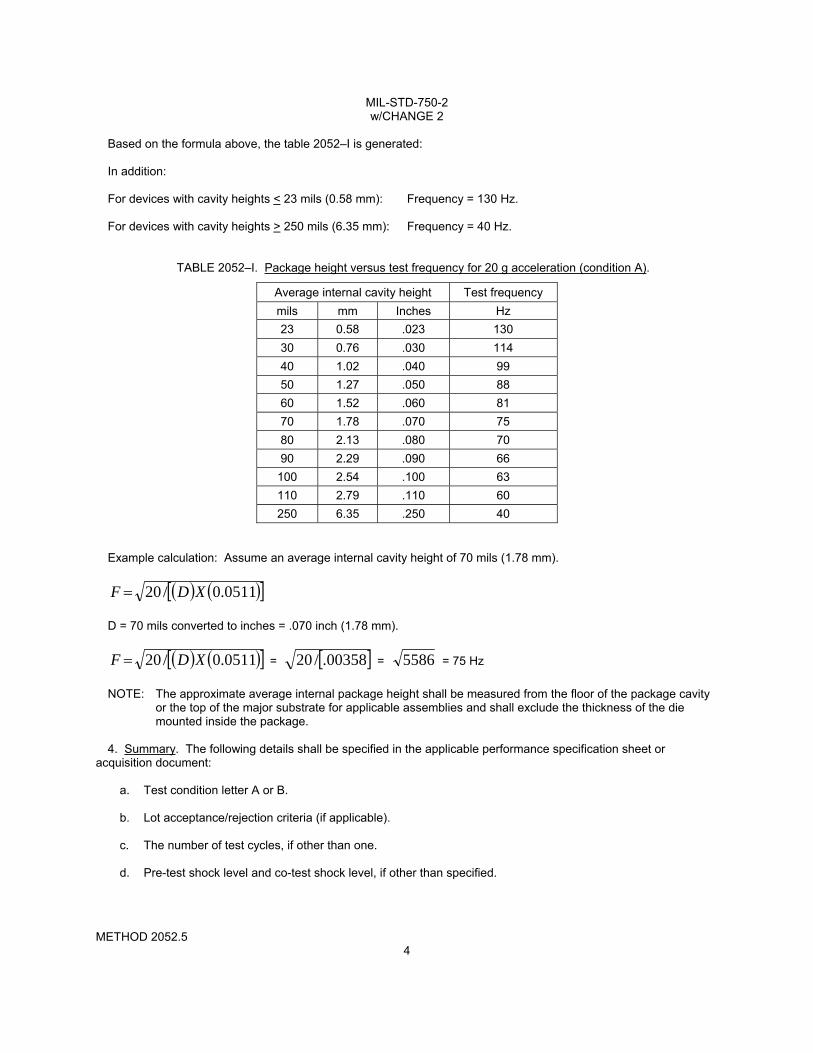
MIL-STD-750-2 w/CHANGE 2
METHOD 2052.5 4
Based on the formula above, the table 2052–I is generated: In addition: For devices with cavity heights < 23 mils (0.58 mm): Frequency = 130 Hz. For devices with cavity heights > 250 mils (6.35 mm): Frequency = 40 Hz.
TABLE 2052–I. Package height versus test frequency for 20 g acceleration (condition A).
Average internal cavity height Test frequency
mils mm Inches Hz
23 0.58 .023 130
30 0.76 .030 114
40 1.02 .040 99
50 1.27 .050 88
60 1.52 .060 81
70 1.78 .070 75
80 2.13 .080 70
90 2.29 .090 66
100 2.54 .100 63
110 2.79 .110 60
250 6.35 .250 40 Example calculation: Assume an average internal cavity height of 70 mils (1.78 mm).
0511.0/20 XDF
D = 70 mils converted to inches = .070 inch (1.78 mm).
0511.0/20 XDF = 00358./20 = 5586 = 75 Hz
NOTE: The approximate average internal package height shall be measured from the floor of the package cavity
or the top of the major substrate for applicable assemblies and shall exclude the thickness of the die mounted inside the package.
4. Summary. The following details shall be specified in the applicable performance specification sheet or
acquisition document:
a. Test condition letter A or B. b. Lot acceptance/rejection criteria (if applicable). c. The number of test cycles, if other than one. d. Pre-test shock level and co-test shock level, if other than specified.
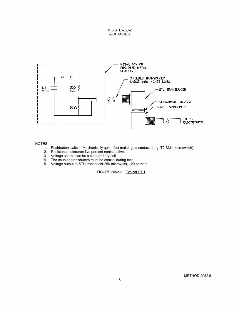
MIL-STD-750-2 w/CHANGE 2
METHOD 2052.5 5
NOTES:
1. Pushbutton switch: Mechanically quiet, fast make, gold contacts (e.g. T2 SM4 microswitch). 2. Resistance tolerance five percent noninductive. 3. Voltage source can be a standard dry cell. 4. The coupled transducers must be coaxial during test. 5. Voltage output to STU transducer 250 microvolts, ±20 percent.
FIGURE 2052–1. Typical STU.

MIL-STD-750-2 w/CHANGE 2
This page is intentionally left blank.

MIL-STD-750-2 w/CHANGE 2
METHOD 2056 1 of 1
METHOD 2056
VIBRATION, VARIABLE FREQUENCY
1. Purpose. The variable-frequency-vibration test method is performed for the purpose of determining the effect on semiconductor devices of vibration in the specified frequency range.
2. Apparatus. Equipment used in this test method shall be capable of demonstrating device conformance to the requirements of the performance specification sheet or acquisition document.
3. Procedure.
3.1 Mounting. The device shall be rigidly fastened on the vibration platform and the leads or cables adequately secured.
3.2 Amplitude. The device shall be subjected to a constant peak acceleration of 20 g minimum.
3.2.1 Frequency range. The vibration frequency shall be varied approximately logarithmically between 100 and 2,000 Hz.
3.2.2 Sweep time and duration. The entire frequency range of 100 to 2,000 Hz and return to 100 Hz shall be traversed in not less than four minutes. This cycle shall be performed 4 times in each of the orientations X, Y, and Z (a total of 12 times), so that the motion shall be applied for a total period of approximately 48 minutes.
4. Summary. The measurements after test shall be specified in the applicable performance specification sheet or acquisition document.

MIL-STD-750-2 w/CHANGE 2
This page is intentionally left blank.

MIL-STD-750-2 w/CHANGE 2
METHOD 2057.2 1 of 1
METHOD 2057.2
VIBRATION, VARIABLE FREQUENCY (MONITORED)
1. Purpose. This test method is performed for the purpose of detecting malfunctions of semiconductor devices during vibration in the specified frequency range at the specified acceleration.
2. Apparatus. Equipment used in this test method shall be capable of demonstrating device conformance to the requirements of the performance specification sheet or acquisition document.
3. Procedure.
3.1 Mounting. The device shall be rigidly fastened on the vibration platform. Special care is required to ensure the position of the electrical connection to the device leads to prevent intermittent contacts during vibration. Care must also be exercised to avoid magnetic fields in the area of the device being vibrated.
3.2 Amplitude. The device shall be vibrated with a simple harmonic motion with a constant peak acceleration of 20 g minimum. The acceleration shall be monitored at a point where the g level is equivalent to that of the support point for the device(s).
3.3 Frequency range. The vibration shall be varied logarithmically between 100 and 2,000 Hz.
3.4 Sweep time and duration. The entire frequency range of 100 to 2,000 Hz and return to 100 Hz shall be traversed in not less than 8 minutes. This frequency range shall be executed at one time in each of the orientations X, Y, and Z (total of 3 times) so that the motion shall be applied for a total of 24 minutes minimum. Interruptions are permitted provided the requirements for rate of change and test duration are met. Completion of vibration within any separate frequency band is permissible before going on to the next band.
4. Measurements. With the specified dc voltages and currents applied, the semiconductor device shall be monitored continuously, during the vibration period, for intermittent opens and shorts. The monitoring equipment shall be capable of detecting voltage or current changes of the duration and magnitude specified on the performance specification sheet. In addition, the equipment shall utilize a positive-indication "go-no go" technique or a recorded trace. Equipment requiring continuous visual monitoring, such as an oscilloscope, shall not be used.
5. Summary. The following conditions shall be specified in the applicable performance specification sheet or acquisition document:
a. Electrical test conditions. b. The duration and magnitude of the voltage or current change. c. Post-test measurements.

MIL-STD-750-2 w/CHANGE 2
This page is intentionally left blank.

MIL-STD-750-2 w/CHANGE 2
METHOD 2066 1 of 1
METHOD 2066
PHYSICAL DIMENSIONS
1. Purpose. The purpose of this test method is to check the physical dimensions of the semiconductor device.
2. Apparatus. Equipment used in this examination shall be capable of demonstrating device conformance to the requirements of the performance specification sheet.
3. Procedure. The semiconductor device shall be examined to verify that the physical dimensions are as specified in the performance specification sheet.
4. Summary. The dimensions which are capable of physically describing the device shall be specified in the applicable performance specification sheet or acquisition document.

MIL-STD-750-2 w/CHANGE 2
This page is intentionally left blank.

MIL-STD-750-2 w/CHANGE 2
METHOD 2068 1 of 1
METHOD 2068
EXTERNAL VISUAL FOR NONTRANSPARENT GLASS–ENCASED,
DOUBLE PLUG, NONCAVITY AXIAL LEADED DIODES
1. Purpose. The purpose of this test method is to visually inspect glass–encased, double plug, noncavity, axial leaded semiconductor devices for cracks which may affect the integrity of the hermetic seal.
2. Apparatus. A binocular microscope with a magnification of 10X to 20X and sufficient lighting for visual inspection of the glass body.
3. Procedure. The examination shall be performed prior to any body coating. The devices shall be examined under a magnification of 10X to 20X for evidence of glass body cracks.
4 Failure criteria. Any device exhibiting cracks in the body glass shall be rejected. Cracks or chipouts in the meniscus area at either end of the body are not cause for rejection.
5. Summary. The following conditions shall be specified in the applicable performance specification sheet or acquisition document:
a. Exceptions or additions to the inspection method. b. Where applicable, any conflicts with approved circuit design topology or construction. c. Where applicable, gauges, drawings, and photographs that are to be used as standards for operator
comparison. d. When applicable, specific magnification.

MIL-STD-750-2 w/CHANGE 2
This page is intentionally left blank.

MIL-STD-750-2 w/CHANGE 2
METHOD 2069.2 1 of 14
METHOD 2069.2
PRE–CAP VISUAL, POWER MOSFET'S
1. Purpose. The purpose of this test method is to verify the construction and quality of workmanship of semiconductor devices in the assembly process to the point of pre–cap inspection. These various inspections and tests are intended to verify compliance with the requirements of the applicable performance specification sheet.
2. Apparatus. The apparatus for this inspection shall consist of the following:
a. Optical equipment capable of the specified magnification(s).
b. Adequate fixturing for handling the devices being inspected without causing damage.
c. Adequate covered storage and transportation containers to protect devices from mechanical damage and environmental contamination.
d. Any visual standards (e.g., drawings, photographs) necessary to enable the inspector to make objective
decisions as to the acceptability of devices being inspected.
3. Procedure.
3.1 General. The devices shall be examined in a suitable sequence of observations with the specified magnification range to determine compliance with the requirements of this test method and the applicable specification sheet.
a. Sequence of inspection. The order in which criteria are presented is not a required order of inspection and may be varied at the discretion of the manufacturer.
b. Inspection control. Within the time interval between visual inspection and preparation for sealing, devices
shall be stored in a controlled environment (i.e., an environment in which air-borne particles and relative humidity are controlled). The use of a positive pressure inert gas environment, such as dry nitrogen, shall satisfy the requirement of storing in a controlled environment. Unless a cleaning operation is performed prior to sealing, devices inspected in accordance with this test method shall be inspected in a class 100,000 environment in accordance with ISO 14644–1 and ISO 14644–2. The maximum allowable relative humidity shall not exceed 65 percent. Devices shall be in clean covered containers when transferred through any uncontrolled environment.
c. Magnification. Inspection shall be performed with either a monocular, binocular, or stereo microscope and
the inspection performed with any appropriate angle, with the device under suitable illumination. Magnification shall be performed within the range of 3X to 100X. All criteria of this test method shall be met for the full range of magnification.
3.2 Bonding inspection (low magnification). This inspection and criteria shall be the required inspection for the
bond type(s) and location(s) to which they are applicable when viewed from above (see figures 2069–1 and 2069–2). (Wire tail is not considered part of the bond when determining physical bond dimensions.) No device shall be acceptable which exhibits any of the following defects.

MIL-STD-750-2 w/CHANGE 2
METHOD 2069.2 2
3.2.1 Gold ball bonds.
a. Gold ball bonds where the ball bond diameter is less than 2 times or greater than 5 times the bonding wire diameter.
b. Gold ball bonds where the wire exit is not completely within the periphery of the ball.
c. Gold ball bonds where the exiting wire is not within boundaries of the bonding pad.
d. Any visible intermetallic formation at the periphery of any gold ball bond.
3.2.2 Wedge bonds.
a. Ultrasonic/thermasonic wedge bonds that are less than 1.2 times or greater than 3.0 times the wire diameter
in width, or are less than 1.5 times or greater than 3.0 times the wire diameter in length, before cutoff, as viewed from above.
b. Thermocompression wedge bonds that are less than 1.2 times or greater than 3.0 times the wire diameter in
width or are less than 1.5 times or greater than 3.0 times the wire diameter in length.
3.2.3 Tailless bonds (crescent).
a. Tailless bonds that are less than 1.2 times or greater than 5.0 times the wire diameter in width, or are less than 0.5 times or greater than 3.0 times the wire diameter in length.
b. Tailless bonds where the bond impression does not cover the entire width of the wire.
3.2.4 General (gold ball, wedge, and tailless). As viewed from above, no device shall be acceptable which exhibits
any of the following defects:
a. Bonds on the die where less than 75 percent of the bond is within the unglassivated bonding pad area (except where due to geometry, the bonding pad is smaller than the bond, the criteria shall be 50 percent).
b. Wire bond tails that extend over and make contact with any metallization not covered by glassivation and not
connected to the wire. c. Wire bond tails that exceed two wire diameters in length at the die bonding pad or four wire diameters in
length at the package or post. d. Bonds on the package post that are not bonded entirely on the flat surface of the post top. e. A bond on top of another bond, bond wire tail, or residual segment of lead wire. An ultrasonic wedge bond
alongside a previous bond where the observable width of the first bond is reduced less than .25 mil (0.006 mm) is considered acceptable.
f. Bonds placed so that the separation between bond and adjacent unglassivated die metallization not
connected to it, is less than 1.0 mil (0.025 mm). g. Rebonding. h. Gold bonds where less than 50 percent of the bond is located within an area that is free of eutectic melt.
MIL-STD-750-2 w/CHANGE 2
METHOD 2069.2 3
3.2.5 Internal lead wires. This inspection and criteria shall be required inspection for the location(s) to which they are applicable when viewed from above. No device shall be acceptable that exhibits any of the following defects:
a. Any wire that comes closer than one wire diameter to unglassivated operating metallization, another wire (common wires excluded), package post, unpassivated die area of opposite polarity, or any portion of the package of opposite polarity including the plane of the lid to be attached (except by design, but in no case should the separation be less than 0.25 mil (0.006 mm)). (Within a 5.0 mil (0.127 mm) spherical radial distance from the perimeter of the bond on the die surface, the separation shall be greater than 1.0 mil (0.025 mm).)
b. Nicks, tears, bends, cuts, crimps, scoring, or neckdown in any wire that reduces the wire diameter by more
than 25 percent, except in bond deformation area. c. Missing or extra lead wires. d. Bond lifting or tearing at interface of pad and wire. e. Any wire which runs from die bonding pad to package post and has no arc or stress relief. f. Wires which cross other wires, except common connectors, except by design, in which case the clearance
shall be 1.0 mil (0.025 mm) minimum. g. Wire(s) not in accordance with bonding diagram (unless allowed in design documentation, for tuning
purposes). h. Kinked wires (an unintended sharp bend) with an interior angle of less than 90 degrees or twisted wires to
an extent that stress marks appear. i. Wire (ball bonded devices) not within 10 degrees of the perpendicular to the surface of the chip for a
distance of greater than 0.5 mil (0.006 mm) before bending toward the package post or other termination point.
3.3 Package conditions (low magnification). No device shall be acceptable which exhibits any of the following
defects.
3.3.1 Foreign material on die surface. All foreign material or particles may be blown off with a nominal gas blow (approximately 20 psig) or removed with a soft camel hair brush. The device shall then be inspected for the following criteria:
a. Loosely attached conductive particles (conductive particles which are attached by less than one-half of their largest dimension) that are large enough to bridge the narrowest unglassivated active metal spacing (silicon chips or any opaque material shall be included as conductive particles).
b. Liquid droplets, chemical stains, or photoresist on the die surface that bridge any combination of
unglassivated metallization or bare silicon areas, except for unused cells. c. Ink on the surface of the die that covers more than 25 percent of a bonding pad area (or interferes with
bonding) or that bridges any combination of unglassivated metallization or bare silicon areas, except for unused cells.

MIL-STD-750-2 w/CHANGE 2
METHOD 2069.2 4
3.3.2 Die mounting.
a. Die to header mounting material which is not visible around at least three sides or 75 percent of the die perimeter. Wetting criteria is not required if the devices pass an approved die attached evaluation test.
b. Any balling of the die mounting material which does not exhibit a fillet when viewed from above. c. Any flaking of the die mounting material. d. Any die mounting material which extends onto the die surface or extends vertically above the top surface of
the die and interferes with bonding.
3.3.3 Die orientation. a. A die which is not oriented or located in accordance with the applicable assembly drawing of the device. b. Die is visibly tipped or tilted (more than 10 degrees) with respect to the die attach surface.
3.3.4 Internal package defects (low magnification inspection) (applicable to headers, bases, caps, and lids). As an
alternative to 100 percent visual inspection of lids and caps in accordance with the criteria of 3.3.1.a, the lids or caps may be subjected to a suitable cleaning process and quality verification procedure approved by the qualifying activity, provided the lids or caps are subsequently held in a controlled environment until capping or preparation for seal.
a. Any header or post plating which is blistered, flaked, cracked, or any combination thereof. b. Any conductive particle which is attached by less than one-half of the longest dimension. c. A bubble or a series of interconnecting bubbles in the glass surrounding the pins which are more than
one-half the distance between the pin and body or pin-to-pin. d. Header posts which are severely bent. e. Any glass, die, or other material greater than 1.0 mil (0.025 mm) in its major dimension which adheres to the
flange or side of the header and would impair sealing. f. Any stain, varnish, or header discoloration which appears to extend under a die bond or wire bond. g. For isolated stud packages:
(1) Any defect or abnormality causing the designed isolating paths between the metal island to be reduced
to less than 50 percent of the design separation.
(2) A crack or chip-out in the substrate.

MIL-STD-750-2 w/CHANGE 2
METHOD 2069.2 5
3.3.5 Carrier defects (substrate (e.g., BeO, alumina)).
a. Any chip-out in the carrier material. b. Carrier metallization which is smeared or is obviously not uniform in metallization design pattern to the
extent that there is less than 50 percent of the original design separation, or 0.5 mil (0.013 mm), whichever is less, between operating pads, paths, lid mounting metallization, edges, or any combination thereof.
c. Any crack in the BeO or operating metallization that would affect hermetic seal or die mounting metallization.
(Tooling marks or cold form interface lines are not cracks and are not cause for rejection.) d. Any metallization lifting, peeling, or blistering (on the carrier surface). e. Any attached conductive foreign material which bridges any combination of metallization paths, leads, or
active circuit elements. f. A scratch or void in the metallization which exposes the substrate anywhere along its length and leaves less
than 75 percent of the original metal width undisturbed.
NOTE: Occasionally package metallization is intentionally burnished or scratched, in areas which require wire bond attachment, to improve surface bondability; such conditions are not cause for rejection. Burnished or scratched areas must satisfy the criteria of 3.3.4.b.
g. Excessive scratches in carrier metallization due to abuse in handling or processing. h. Any staple, bridge, or clip with solder joint which exhibits less than 50 percent wetting around the section
that is attached to the package. i. Any header post(s) which are not perpendicular within 10 degrees of the horizontal plane of the header. j. Any lead attach eutectic or solder which extends across greater than 50 percent of the design separation
gap between metallization pads.
3.3.6 Presence of extraneous matter. Extraneous matter (foreign particles) shall include, but not be limited to:
a. Any foreign particle, loose or attached, greater than 3.0 mil (0.076 mm) or of any lesser size which is sufficient to bridge nonconnected conducting elements of the device.
b. Any wire tail extending beyond its normal end by more than two diameters at the semiconductor die pad or
by more than four wire diameters at the package post (see figure 2069–3). c. Any burr on a post (header lead) greater than 3.0 mil (0.076 mm) in its major dimension or of such
configuration that it may break away. d. Excessive semiconductor die bonding material buildup. A semiconductor die shall be mounted and bonded
so that it is not tilted more than 10 degrees from mounting surface. The bonding agent that accumulates around the perimeter of the semiconductor die and touches the side of the semiconductor die shall not accumulate to a thickness greater than that of the semiconductor die (see figures 2069–1 and 2069–5). Where the bonding agent is built up but is not touching the semiconductor die, the build up shall not be greater than twice the thickness of the semiconductor die. There shall be no excess semiconductor die bonding material in contact with the active surface of the semiconductor die or any lead or post, or separated from the main bonding material area (see figure 2069–6).
e. Flaking on the header or posts or anywhere inside the case. f. Extraneous ball bonds anywhere inside case, except for attached bond residue when rebonding is allowed.

MIL-STD-750-2 w/CHANGE 2
METHOD 2069.2 6
3.4 Semiconductor conditions. No device shall be acceptable which exhibits any of the following defects.
3.4.1 Metallization, scratches, and voids exposing underlying material.
a. A scratch or void that severs the innermost guard ring. b. Any die containing a void in the metallization at the bonding pad covering more that 25 percent of the pad
area. c. For devices with non-expanded contacts and all power devices. Any scratch or void which isolates more
than 25 percent of the total metallization of an active region from the bonding pad. d. For all devices with expanded contacts. A scratch or void, whether or not underlying material is exposed,
which leaves less than 50 percent undisturbed metal width in the metal connecting the pad and the contact regions.
e. For expanded contacts with less than or equal to 10 contact regions. A scratch or void extending across
more than 50 percent of the first half of any contact region (beginning at the bonding area) in more than 10 percent of the contact regions.
f. For expanded contacts with less than or equal to 10 contact regions. A scratch or void in the contact area
which isolates more than 10 percent of the metallized area form the bonding area.
3.4.2 Metallization corrosion. Any metallization which shows evidence of corrosion.
3.4.3 Metallization adherence. Any metallization which has lifted, peeled, or blistered.
3.4.4 Metallization probe marks. Criteria found in 3.4.1 shall apply as limitations for probing damage.
3.4.5 Metallization bridging. Metallization bridging between two normally unconnected metallization paths which reduces the separation, such that a line of oxide is not visible (no less than 0.1 mil (0.003 mm)) when viewed at the prescribed magnification.
3.4.6 Metallization alignment.
a. Except by design, contact window that has less than 50 percent of its area covered by continuous metallization.
b. A metallization path not intended to cover a contact window which is separated from the window by less
than 0.1 mil (0.003 mm).
3.4.7 Passivation faults.
a. Any passivation fault including pinholes not covered by glassivation that exposes semiconductor material and allows bridging between any two diffused areas, any two metallization strips, or any such combination not intended by design.
b. Except by design, an absence of passivation visible at the edge and continuing under the metallization
causing an apparent short between the metal and the underlying material (closely spaced double or triple lines on the edges of the defect indicate that it may have sufficient depth to penetrate down to the silicon).
c. Except by design, any active junction not covered by passivation or glassivation.

MIL-STD-750-2 w/CHANGE 2
METHOD 2069.2 7
3.4.8 Scribing and other die defects.
a. Except by design, less than 0.1 mil (0.003 mm) passivation visible between active metallization or bond pad
periphery and the edge of the die. b. Any chip-out or crack in the active area. c. Except by design, die having attached portions of the active area on another die, and which exceeds 10
percent of the area of the second die. d. Any crack which extends 2.0 mils (0.051 mm) in length inside the scribe grid or scribe line that points toward
active metallization or active area and extends into the oxide area. e. Any chip-out that extends to within 1.0 mil (0.025 mm) of a junction. f. Any crack or chip-out that extends under any active metallization area. g. Any chip-out which extends completely through the guard ring.
3.4.9 Glassivation defects.
a. Glass crazing that prohibits the detection of visual criteria contained herein. b. Any glassivation which has delaminated. (Lifting or peeling of the glassivation may be excluded from the
criteria above, when it does not extend more than 1.0 mil (0.025 mm) from the designed periphery of the glassivation, provided that the only exposure of metal is adjacent to bond pads or of metallization leading from those pads.)
c. Except by design, two or more adjacent active metallization paths which are not covered by glassivation. d. Unglassivated areas at the edge of bonding pad which expose silicon. e. Glassivation which covers more than 25 percent of the design bonding pad area.
3.5 Post protective coating visual inspection. If devices are to be coated with a protective coating, the devices
shall be visually examined in accordance with the criteria specified in 3 herein, prior to the application of the coating. After the application and cure of the protective coating, the devices shall be visually examined under a minimum of 10X magnification. No device shall be acceptable which exhibits any of the following defects:
a. Except by design, any unglassivated or passivated areas or insulating substrate which has incomplete age. b. Open bubbles, cracks, or voids in the protective coating. c. A bubble, or a chain of bubbles, which covers two adjacent metallized surfaces. d. Protective coating which has flaked or peeled. e. Protective coating which is not fully cured. f. Conductive particles which are embedded in the coating and are large enough to bridge the narrowest
unglassivated active metal spacing (silicon chips shall be included as conductive particles). g. Except by design, a web of protective coating that connects the wire with the header.

MIL-STD-750-2 w/CHANGE 2
METHOD 2069.2 8
4. Summary. The following details shall be specified in the applicable performance specification sheet or
acquisition document:
a. Exceptions or additions to the inspection method. b. Where applicable, any conflicts with approved circuit design topology or construction. c. Where applicable, gauges, drawings, and photographs that are to be used as standards for operator
comparison. d. When applicable, specific magnification.

MIL-STD-750-2 w/CHANGE 2
METHOD 2069.2 9
A. Tailless or crescent.
NOTES: 1. 1.2 D W 5.0 D (width). 2. 0.5 D L 3.0 D (length).
Ultrasonic Thermocompression
B. Wedge.
NOTES: NOTES:
1. 1.0 D ≤ W ≤ 3.0 D (width). 1. 1.2 D ≤ W ≤ 3.0 D (width). 2. 1.5 D ≤ L ≤ 3.0 D (length). 2. 1.5 D ≤ L ≤ 3.0 D (length).
FIGURE 2069–1. Bond dimensions.

MIL-STD-750-2 w/CHANGE 2
METHOD 2069.2 10
FIGURE 2069–2. Torn bonds.

MIL-STD-750-2 w/CHANGE 2
METHOD 2069.2 11
FIGURE 2069–3. Acceptable and unacceptable voids and excessive pigtails.

MIL-STD-750-2 w/CHANGE 2
METHOD 2069.2 12
FIGURE 2069–4. Acceptable and unacceptable bonding material build-up.

MIL-STD-750-2 w/CHANGE 2
METHOD 2069.2 13
FIGURE 2069–5. Extraneous bonding material build-up.

MIL-STD-750-2 w/CHANGE 2
METHOD 2069.2 14
FIGURE 2069–6. Acceptable and unacceptable excess material.
MIL-STD-750-2 w/CHANGE 2
METHOD 2070.2 1 of 18
METHOD 2070.2
PRE–CAP VISUAL
MICROWAVE DISCRETE AND MULTICHIP TRANSISTORS
1. Purpose. The purpose of this test method is to verify the construction and quality of workmanship in wafer, wafer dc testing, die inspection, and assembly processes to the point of semiconductor device pre–cap inspection. These various inspections and tests are intended to detect and remove transistor die with defects that could lead to semiconductor device failure during application and to verify compliance with the requirements of the applicable performance specification sheet or acquisition document.
2. Apparatus. The apparatus for this test method shall consist of the following:
a. Optical equipment capable of the specified magnifications, and both normal incident and darkfield lighting. b. Adequate fixturing for handling the devices being inspected without causing damage. c. Adequate covered storage and transportation containers to protect devices from mechanical damage and
environmental contamination. d. Any visual standards (e.g., drawings, photographs) necessary to enable the inspector to make objective
decisions as to the acceptability of devices being inspected.
2.1 Microwave devices. GaAs microwave devices shall be inspected to all applicable criteria as listed herein. GaAs microwave devices shall also have additional specific criteria as listed and the applicable high power magnification for individual features of GaAs microwave devices shall be selected from table 2070–I.
TABLE 2071–I. GaAs microwave device high magnification requirements.
Feature dimensions Magnification range
> 5 microns 75 – 150X
1 – 5 microns 150 – 400X
< 1 micron 400 – 1000X
3. Procedure.
3.1 General. The devices shall be examined in a suitable sequence of observations with the specified magnification range to determine compliance with the requirements of this document and the applicable specification sheet.
a. Sequence of inspection. The order in which criteria are presented is not a required order of inspection and may be varied at the discretion of the manufacturer.
b. Inspection control. Within the time interval between visual inspection and preparation for sealing, devices
shall be stored in a controlled environment (an environment in which air-borne particles and relative humidity are controlled). The use of a positive pressure inert gas environment, such as dry nitrogen, shall satisfy the requirement of storing in a controlled environment. Unless a cleaning operation is performed prior to sealing, devices inspected in accordance with this test method shall be inspected in a class 100,000 environment in accordance with ISO 14644–1 and ISO 14644–2. The maximum allowable relative humidity shall not exceed 65 percent. Devices shall be in clean covered containers when transferred through any uncontrolled environment.

MIL-STD-750-2 w/CHANGE 2
METHOD 2070.2 2
c. Magnification. High magnification inspection shall be performed perpendicular to the die surface with normal
incident or darkfield illumination as required. Low magnification inspection shall be performed with either a monocular, binocular, or stereo microscope and the inspection performed with any appropriate angle, with the device under suitable illumination. High magnification may be used to verify a discrepancy which has first been noted at low magnification.
(1) High magnification inspection shall be performed within the range of 60X to 200X. (2) Low magnification shall be performed within the range of 30X to 60X.
d. General reject criteria. Unless otherwise specified, reject if the defect is present in 25 percent of any one
cell or in 10 percent of the entire die. Figures 2070–1 through 2070–4 illustrate accept and reject criteria for die and bonds.
e. Figures 2070–5 through 2070–7 illustrate different geometries used in fabricating microwave discrete
transistors.
3.2 Wafer inspection. Not applicable.
3.2.1 Metallization inspection. Unless otherwise specified, the 25 percent of a cell and 10 percent of a die reject conditions apply. No die shall be acceptable which exhibits any of the following defects:
a. Metallization misalignment so that there is less than 75 percent coverage of the ohmic contact windows. b. Contact window that has less than a continuous 50 percent of its perimeter covered by metallization.
NOTE: Metal coverage is not required at the far dielectric steps of the end base contacts under base
metal finger tips. c. Metal must cover 50 percent of the contact that lies over the enhancement area. d. Metallization bridging, between two normally unconnected metallization paths, which reduces the design
separation to less than 50 percent or 0.1 mil (0.003 mm) whichever is less. e. Metallization corrosion. Any metallization which shows evidence of corrosion. f. Metallization adherence. Any metallization which has lifted, peeled, or blistered. g. Exception: Do not reject for missing or defective run around metal (run around metal is non active metal
used for probing purposes with multicell devices).

MIL-STD-750-2 w/CHANGE 2
METHOD 2070.2 3
3.2.2 Glassivation and silicon nitride defects. (Unless otherwise specified, the 25 percent of a cell and 10 percent of a die reject conditions apply). No die shall be acceptable which exhibits any of the following defects:
a. Glass crazing that prohibits the detection of voids or scratches during subsequent inspection or that covers more than 25 percent of the die area.
b. Any glassivation which has delaminated. c. Two or more adjacent active metallization paths which are not covered by glassivation, except by design. d. Unglassivated areas at the edge of bonding pads which expose silicon. e. Glassivation which covers more than 25 percent of the designed bonding pad area. f. Glass crazing covering more than 25 percent of the die area. g. Glass cracks which form closed loops over adjacent metallization paths.
3.3 Die metallization defects (high magnification). No die shall be acceptable which exhibits any of the following
defects.
3.3.1 Metallization scratches and voids exposing underlying material (see figure 2070–1). Unless otherwise specified, the 25 percent of a cell and 10 percent of a die conditions apply.
a. A scratch or void that severs the innermost metallized guard ring. b. Any die containing a void in the metallization at the bonding pad covering more than 25 percent of the pad
area (see figure 2070–1). c. For all devices with expanded contacts. A scratch, whether or not underlying material is exposed; or a void,
which leaves less than 50 percent undisturbed metal width in the metal connecting the pad and the contact regions.
d. For expanded contacts with more than 10 contact regions. A scratch or void extending across more than 50
percent of the first half of any contact region (beginning at the bonding area) in more than 10 percent of the contact regions.
e. For expanded contacts with less than 10 contact regions. A scratch or void in the contact area which
isolates more than 10 percent of the contact regions. f. Metallization probing. Criteria contained in 3.3.1.b shall apply as limitation on probing damage.

MIL-STD-750-2 w/CHANGE 2
METHOD 2070.2 4
3.4 Scribing and die defects (high magnification) (see figure 2070–2). No device shall be acceptable which exhibits any of the following defects:
a. Unless by design, less than 0.1 mil (0.003 mm) passivation visible between active metallization or bond pad periphery and the edge of the die.
b. Any chip-out or crack in the active area. c. Any crack which exceeds 2.0 mils (0.051 mm) in length beyond the scribe grid or line that points toward
active metallization or an active area. d. Any chip-out that extends to within 1.0 mil (0.025 mm) of an active area or to within 50 percent of the design
spacing, whichever is less. e. Any crack or chip-out that extends under any active metallization. f. Reject if more than 25 percent of a depletion ring is missing. A depletion ring encompasses an individual
cell. An annular ring encompasses the entire die. A true annular ring will be the same color as the emitter.
3.5 Bonding inspection (low magnification). This inspection and criteria shall be the required inspection for the bond types and locations to which they are applicable when viewed from above (see figures 2070–3 and 2070–4). (Wire tail is not considered part of the bond when determining physical bond dimensions.) No device shall be acceptable which exhibits any of the following defects.
3.5.1 Gold ball bonds.
a. Gold ball bonds where the ball bond diameter is less than 2.0 times or greater than 5.0 times the bonding wire diameter.
b. Gold ball bonds where the wire exit is not completely within the periphery of the ball. c. Gold ball bonds where the exiting wire is not within boundaries of the bonding pad. d. Any visible intermetallic formation at the periphery of any gold ball bond.
3.5.2 Tailless or crescent bonds.
a. Tailless bonds that are less than 1.2 times or greater than 5.0 times the wire diameter in width or are less
than 0.5 times or greater 3.0 times the wire diameter in length. b. Tailless bonds where the bond impression does not cover the entire width of the wire.
3.5.3 Wedge bonds.
a. Aluminum wire: Ultrasonic/thermasonic wedge bonds that are less than 1.2 times or greater than 3.0 times
the wire diameter in width, or less than 1.5 times or greater than 3.0 times the wire diameter in length. b. Gold wire: Ultrasonic/thermasonic wedge bonds that are less than 1.0 times or greater than 3.0 times the
wire diameter in width, or less than 0.5 times or greater than 3.0 times the wire diameter in length. c. Thermocompression wedge bonds that are less than 1.2 times or greater than 3.0 times the wire diameter in
width or are less than 0.5 times or greater than 3.0 times the wire diameter in length.

MIL-STD-750-2 w/CHANGE 2
METHOD 2070.2 5
3.5.4 General (gold ball, wedge, and tailless). As viewed from above, no device shall be acceptable which exhibits
any of the following defects:
a. Bonds on the die where less than 50 percent of the bond is within the unglassivated bonding pad area. b. Wire bond tails that extend over and make contact with any metallization not covered by glassivation and not
connected to the wire. c. Wire bond tails that exceed two wire diameters in length at the die bonding pad or four wire diameters in
length at the package or post. d. Bonds on the package post that are not bonded entirely on the flat surface of the post top. e. A bond on top of another bond, bond wire tail, or residual segment of lead wire. An ultrasonic wedge bond
alongside a previous bond where the observable width of the first bond is reduced less than .25 mil (0.006 mm) is considered acceptable.
f. Bonds placed so that the separation between bond and adjacent unglassivated die metallization not
connected to it is less than 1.0 mil (0.025 mm), except if the glass does not exhibit cracking, the separation may be 0.1 mil (0.003 mm).
g. Rebonding shall be permitted with the following limitations.
(1) No scratched, open, or discontinuous metallization paths or conductor patterns shall be repaired by bridging with, or addition of, bonding wire or ribbon.
(2) All rebonds shall be placed on at least 50 percent undisturbed metal (excluding probe marks that do not
expose oxide) and no more than one rebond attempt at any design bond location shall be permitted at any pad or post and no rebonds shall touch an area of exposed oxide caused by lifting metal.
(3) The total number of rebond attempts shall be limited to a maximum of 10 percent of the total number of
bonds in the device. The 10 percent limit on rebonds may be interpreted as the nearest whole number of bonds in the device. A bond shall be defined as a wire to post or wire to bond pad. Bond-offs required to clear the bonder after an unsuccessful first bond attempt need not be considered as rebonds provided they can be identified as bond-offs by being made physically away from normal bond areas. The initial bond attempt need not be visible. A replacement of one wire at one end or an unsuccessful bond attempt at one end of the wire counts as one rebond. A replacement of wire bonded at both ends or an unsuccessful bond attempt of a wire already bonded at the other end counts as two rebonds.
h. Gold bonds where less than 50 percent of the bond is located within an area that is free of eutectic melt.
The blush area shall not be considered part of the eutectic melt. (The blush area is defined as the area where a color change can be seen but not a change in surface texture.)
MIL-STD-750-2 w/CHANGE 2
METHOD 2070.2 6
3.5.5 Internal lead wires. This inspection and criteria shall be required inspection for the locations to which they are applicable when viewed from above. No device shall be acceptable that exhibits any of the following defects.
a. Any wire that comes closer than one wire diameter to unglassivated operating metallization, another wire (common wires excluded), package post, unpassivated die area of opposite polarity, or any portion of the package of opposite polarity including the plane of the lid to be attached (except by design, but in no case should the separation be less than 0.25 mil (0.006 mm)). (Within a 5.0 mil (0.127 mm) spherical radial distance from the perimeter of the bond on the die surface, the separation shall be greater than 1.0 mil (0.025 mm).)
b. Nicks, tears, bends, cuts, crimps, scoring, or neckdown in any wire that reduces the wire diameter by more
than 25 percent, except in bond deformation area. c. Missing or extra lead wires. d. Bond lifting or tearing at interface of pad and wire. e. Any wire which runs from die bonding pad to package post and has no arc or stress relief. f. Wires which cross other wires, except common connectors, except by design, in which case the clearance
shall be 1.0 mil (0.025 mm) minimum. g. Wires not in accordance with bonding diagram (unless allowed in design documentation, for tuning
purposes). h. Kinked wires (an unintended sharp bend) with an interior angle of less than 90 degrees or twisted wires to
an extent that stress marks appear. i. Wire (ball bonded devices) not within 10 degrees of the perpendicular to the surface of the chip for a
distance of greater than 0.5 mil (0.013 mm) before bending toward the package post or other termination point.
3.6 Package conditions (low magnification). No device shall be acceptable which exhibits any of the following
defects.
3.6.1 Foreign material on die surface. All foreign material or particles may be blown off with a nominal gas blow (approximately 20 psi (138 kPa)) or removed with a soft camel hair brush. The device shall then be inspected for the following criteria.
a. Loosely attached conductive particles (conductive particles which are attached by less than one-half of their largest dimension) that are large enough to bridge the narrowest unglassivated active metal spacing (silicon chips or any opaque material shall be included as conductive particles).
b. Liquid droplets, chemical stains, or photoresist on the die surface that bridge any combination of
unglassivated metallization or bare silicon areas, except for unused cells. c. Ink on the surface of the die that covers more than 25 percent of a bonding pad area (or interferes with
bonding) or that bridges any combination of unglassivated metallization or bare silicon areas, except for unused cells.
d. Any entrapped opaque material which appears to extend over metallization.

MIL-STD-750-2 w/CHANGE 2
METHOD 2070.2 7
3.6.2 Die mounting.
a. Die to header mounting material which is not visible around at least three sides or 75 percent of the die perimeter. Wetting criteria is not required if the devices pass an approved die attached evaluation test.
b. Any balling of the die mounting material which does not exhibit a fillet when viewed from above. c. Any flaking of the die mounting material. d. Any die mounting material which extends onto the die surface beyond the scribe zone and comes closer
than 0.5 mil (0.013 mm) to any active area or metallization, or extends vertically above the top surface of the die and interferes with bonding.
3.6.3 Die orientation.
a. A die which is not oriented or located in accordance with the applicable assembly drawing of the device. b. Die is visibly tipped or tilted (more than 10 degrees) with respect to the die attach surface.
3.6.4 Internal package defects (applicable to headers, bases, caps, and lids). As an alternative to 100-percent
visual inspection, the lids or caps may be subjected to a suitable cleaning process and quality verification procedure approved by the qualifying activity, provided the lids or caps are subsequently held in a controlled environment until capping or preparation for seal.
a. Any header or post plating which is blistered. b. Any conductive particle which is attached by less than one-half of the longest dimension. c. For isolated heat sink packages:
(1) Any defect or abnormality causing the designed isolating paths between the metal islands to be reduced
to less than 50 percent of the design separation or reduced to 0.2 mil (0.005 mm), whichever is less. (2) A crack in the substrate.
3.6.5 Carrier defects ((e.g., BeO, alumina) substrate).
a. Any chip-out in the carrier material. b. Carrier metallization which is smeared or is obviously not uniform in metallization design pattern to the
extent that there is less than 50 percent of the original design separation, or 0.5 mil (0.013 mm), whichever is less, between operating pads, paths, lid mounting metallization, edges, or any combination thereof.
c. Any crack in the BeO or operating metallization that would affect hermetic seal or die mounting metallization.
(Tooling marks or cold form interface lines are not cracks and are not cause for rejection.) d. Any metallization lifting, peeling, or blistering (on the carrier surface). e. Any attached conductive foreign material which bridges any combination of metallization paths, leads, or
active circuit elements.

MIL-STD-750-2 w/CHANGE 2
METHOD 2070.2 8
f. A scratch or void in the metallization which exposes the substrate anywhere along its length and leaves less than 75 percent of the original metal width undisturbed.
NOTE: Occasionally package metallization is intentionally burnished or scratched, in areas which require
wire bond attachment, to improve surface bondability; such conditions are not cause for rejection. Burnished or scratched areas must satisfy the criteria of 3.6.4.b.
g. Excessive scratches in carrier metallization due to abuse in handling or processing. h. Any staple, bridge, or clip with solder joint which exhibits less than 50 percent wetting around the section
that is attached to the package. i. Any header posts which are not perpendicular within 10 degrees of the horizontal plane of the header. j. Any lead attach eutectic or solder which extends across greater than 50 percent of the design separation
gap between metallization pads.
3.7 Capacitor defects (high magnification).
a. Scratches through the metal that extend the length of the metal and expose underlying oxide. b. Any metallization peeling (except due to bond tail pull). c. Any metallization which shows evidence of corrosion. d. Cracks in the silicon that point toward the metal and are within 1.0 mil (0.025 mm) of the metal (except for
ground bar portion). e. Chip-outs within 0.5 mil (0.013 mm) of the metal (except for ground bar portion). f. Metal that has been gouged or probed over 20 percent of a bonding pad area and exposes underlying oxide. g. Mounting material which is not visible around at least three sides or 75 percent of the capacitor perimeter.
Wetting criteria is not required if the devices pass an approved capacitor attach evaluation test. (This inspection is to be performed at low magnification.)
NOTE: Multiple bonding is allowable for tuning purposes, however initial bond wire shall be completely
removed before rebonding and must be in accordance with design documentation.
3.8 Alignment (this applies to 25 percent of any one cell or 10 percent of any die). Reject any diffusion line which touches another diffusion line, except for contact enhancements, which can touch an active area of the same type. Emitter contacts can touch emitter base junction but cannot cross. Base contacts must engage 50 percent or more of the contact enhancement. NOTE: Contacts are not diffused.

MIL-STD-750-2 w/CHANGE 2
METHOD 2070.2 9
3.9 Resistors (criteria applies to 25 percent of any one cell or 10 percent of any die). The requirements for resistors shall be in accordance with table 2070–II.
TABLE 2070–II. Resistor criteria.
Process level Defect Reject
Nickel-Chromium (NICR) resistor
Pinched Resistor is less than 90 percent of its intended design width.
Undercutting Resistor is less than 75 percent of its intended design width. Bridging or excess NICR Bridging between discrete resistor pattern.
Diffused resistors Oxide defects Poor definitions
No visible opening.
Misalignment Contacting less than 90 percent of its intended design width. Undercutting Resistor less than 75 percent of its intended design width. Over etched Resistor is greater than 125 percent of its intended design width. Poly SI resistor Pinched Resistor is less than 90 percent of its intended design width. Poly SI resistor Undercut Resistor is less than 75 percent of its intended design width. Bridging or excess poly SI Bridging between discrete resistor pattern. Misalignment Contacting less than 75 percent of the design separation. NOTE: Reject if 25 percent of any one cell or 10 percent of any die exhibits burned or missing resistors.
3.9.1 NICR resistor. Thin film deposited and patterned usually connecting emitter fingers to emitter feed metal to control current. It can also be used as a passive element in RF IC's.
3.9.2 Poly SI resistors (bevel). Thin film of poly SI is deposited, doped, and patterned usually connecting emitter fingers to emitter feed metal to control current. It can also be used as passive elements in RF IC's.
3.9.3 Diffused resistors (contact appearance). A diffused area connecting emitter fingers to emitter feed metal used to control current.
3.9.4 Contacts and diffusion defects (contacts are not diffused). Reject if contacts are less than 50 percent of design on 10 percent of the die. Reject any die that has a discontinuous implant or diffusion line effecting more than 10 percent of the die. A discontinuous line is a line that wanders but does not close on itself. Reject any die where an implant or diffusion fault bridges between two diffuse areas, any two metallized stripes of any combination not intended by design. This must effect greater than 10 percent of the die. Reject any implant or diffused area that is less than 50 percent of design.
3.9.5 Passivation or oxide defects. This applies to 25 percent of a cell and 10 percent of the die. Reject any active junction not covered by passivation or glassivation. Reject for absence of passivation or oxide visible at the edge and continuing under the metallization causing a short between the metal and the underlying material (unless by design). Reject for passivation or oxide defects that allows bridging between any two metallized stripes.
4. Summary. The following conditions shall be specified in the applicable performance specification sheet:
a. Exceptions or additions to the inspection method. b. Where applicable, any conflicts with approved circuit design topology or construction. c. Where applicable, gauges, drawings, and photographs that are to be used as standards for operator
comparison. d. When applicable, specific magnification.

MIL-STD-750-2 w/CHANGE 2
METHOD 2070.2 10
FIGURE 2070–1. Metallization scratches and voids (expanded contact).

MIL-STD-750-2 w/CHANGE 2
METHOD 2070.2 11
FIGURE 2070–2. Cracks and chips.

MIL-STD-750-2 w/CHANGE 2
METHOD 2070.2 12
NOTES:
1. 1.2 D ≤ W ≤ 5.0 D (width) 2. 0.5 D ≤ L ≤ 3.0 D (length)
NOTES: NOTES:
1. 1.0 D ≤ W ≤ 3.0 D (width) 1. 1.2 D ≤ W ≤ 3.0 D (width) 2. 1.5 D ≤ L ≤ 5.0 D (length) 2. 1.5 D ≤ L ≤ 5.0 D (length)
FIGURE 2070–3. Bond dimensions.

MIL-STD-750-2 w/CHANGE 2
METHOD 2070.2 13
FIGURE 2070–4. Lifted or torn bonds.

MIL-STD-750-2 w/CHANGE 2
METHOD 2070.2 14
FIGURE 2070–5. Mesh geometry.

MIL-STD-750-2 w/CHANGE 2
METHOD 2070.2 15
FIGURE 2070–5. Mesh geometry – Continued.
MIL-STD-750-2 w/CHANGE 2
METHOD 2070.2 16
FIGURE 2070–6. Interdigitated geometry.

MIL-STD-750-2 w/CHANGE 2
METHOD 2070.2 17
FIGURE 2070–7. Spine geometry.
MIL-STD-750-2 w/CHANGE 2
METHOD 2070.2 18
FIGURE 2070–7. Spine geometry – Continued.

MIL-STD-750-2 w/CHANGE 2
This page is intentionally left blank.

MIL-STD-750-2 w/CHANGE 2
METHOD 2071.7 1 of 14
METHOD 2071.7
VISUAL AND MECHANICAL EXAMINATION
1. Purpose. The purpose of this test method is to verify the workmanship of hermetically packaged semiconductor devices. This method shall also be utilized to inspect for damage due to handling, assembly, and test of the packaged device. This test method is normally employed at outgoing inspection within the device manufacturer’s facility, or as an incoming inspection of the assembled device.
2. Apparatus. Apparatus used in this test method shall be capable of demonstrating device conformance to the applicable requirements of the individual specification sheet. This includes optical equipment capable of magnification of 20X minimum as specified herein, which shows the entire area of interest at once in the field of view. The preferred instrument is a binocular microscope with 10X eye pieces and 1.0X objective having a magnification range between 20X and 40X.
3. Procedure. Unless otherwise specified, the device shall be examined under a magnification of 20X minimum. The field of view shall be sufficiently large to contain the entire device and allow inspection to the criteria listed in 3.1. Where inspection at a lower magnification reveals an anomaly, then inspection at a higher magnification (40X maximum, unless otherwise specified) may be performed to determine acceptability. Higher magnification may be used to further examine and characterize observed anomalies.
When a disposition is in doubt for any dimensional criteria, that dimension may be measured for verification.
3.1 Failure criteria. Devices which exhibit any of the following conditions shall be considered rejects.
3.1.1 General rejects. Device construction (package outline), lead (terminal), identification, markings (content, placement, and legibility), and workmanship not in accordance with the applicable performance specification sheet shall be rejected. This includes the following:
a. Any misalignment of device component parts to the extent that the package outline drawing dimensions are exceeded.
b. Visual evidence of corrosion or contamination. Discoloration is not sufficient cause for rejection. The
presence of lead carbonate formations in the form of a white/yellow crystalline shall be considered evidence of contamination.
c. Damaged or bent leads or terminals which precludes their use in the intended application. d. Defective finish: Mechanical damage which exposes underplate or base metal. Evidence of blistering,
non-adhesion, peeling, or flaking of the finish which exposes underplate or base metal. e. Burrs that will cause lead or terminal dimensions to be exceeded. f. Foreign material (including solder or other metallization) bridging leads or otherwise interfering with the
normal application of the device. Where adherence of foreign material is in question, devices may be subjected to a clean filtered air stream (suction or expulsion) or an isopropyl alcohol wash and then reinspected.
g. Protrusions beyond seating plane that will interfere with proper seating of the device. h. Missing welds or crimps. i. Damage causing distortion of a flange beyond its normal configuration.

MIL-STD-750-2 w/CHANGE 2
METHOD 2071.7 2
j. Damage to a stud (thread damage or bending) which restricts normal mounting. k. Dents in metal lids which precludes their use in the intended application or causing a defect in the finish (see
3.1.1.d). l. Gaps, separations, or other openings that are not part of the normal design configuration. m. Tubulation weld: Any fracture or split in the tubulation weld. n. Weld alignment: Base weld mating surfaces not parallel, or that precludes intended use.
3.1.1.1 Failure criteria for lead/terminal seal area of metal can devices.
a. Radial cracks (except meniscus cracks) that extend more than one-half of the distance from the pin to the
outer member (see figure 2071–1). Radial cracks that originate from the outer member. b. Circumferential cracks (except meniscus cracks) that extend more than 90 degrees around the seal center
(see figure 2071–2). c. Open surface bubble(s) in strings or clusters that exceed two-thirds of the distance between the lead and the
package wall. d. Visible subsurface bubbles that exceed the following:
(1) Large bubbles or voids that exceed one-third of the glass sealing area (see figure 2071–3). (2) Single bubble or void that is larger than two-thirds of the distance between the lead and the package
wall at the site of the inclusion and extends more than one-third of the glass seal depth (see figure 2071–4).
(3) Two bubbles in a line totaling more than two-thirds of the distance from pin to case (see figure 2071–5). (4) Interconnecting bubbles greater than two-thirds of the distance between pin and case
(see figure 2071–6). e. Except as designed, re-entrant seals which exhibit non-uniform wicking or negative wicking. f. Twenty-five percent or greater of the radius length from the center of the feedthrough to the edge of the
glass eyelet. g. Glass meniscus cracks that are not located within one-half of the distance between the lead to the case
(see figure 2071–7). The glass meniscus is defined as that area of glass that wicks up the lead or terminal. h. Any chip-out of ceramic or sealing glass that penetrates the sealing glass deeper than the glass meniscus
plane. Exposed base metal as a result of meniscus chip outs are acceptable if the exposed area is no deeper than .010 inch (0.25 mm) or 50 percent of lead diameter, whichever is greater (see figure 2071–8).
3.1.1.2 Failure criteria for ceramic packages. The failure criteria for ceramic packages shall be in accordance with
test method 2009 of MIL–STD–883).
3.1.1.3 Failure criteria for opaque glass body devices. The failure criteria for opaque glass body devices shall be in accordance with test method 2068 of this standard).

MIL-STD-750-2 w/CHANGE 2
METHOD 2071.7 3
3.1.1.4 Transparent glass diodes, double plug construction.
a. Any evidence of a crack, fracture, or a chipout closer to the die than 50 percent of the designed seal length
shall be rejected. Area of examination shall be as shown on figure 2071–9. b. Any crack that terminates in the axial direction is cause for rejection. c. Meniscus cracks are not cause for rejection. d. Any chip out that exposes base metal shall be rejected. e. Small surface impact marks, "c" cracks, and microcracks are acceptable if they are confined to the glass
surface with no other cracks radiating from them. f. Terminals that are not brazed to the plug around at least 90 percent of the terminal perimeter are cause for
rejection.
3.1.1.5 Transparent glass diodes, large cavity (i.e. S-bend, C-bend, or straight-through constructions). Any crack or fracture in the glass over the area of the device cavity shall be rejected.
a. Any crack or fracture in the glass over the area of the device cavity shall be rejected. b. Any chip out that exposes base metal shall be rejected (this does not apply to chip outs at either end of
device where glass joins external lead). c. Any crack that terminates in the axial direction is cause for rejection. d. Meniscus cracks are not cause for rejection. e. Small surface impact marks, "c" cracks, and microcracks are acceptable if they are confined to the glass
surface with no other cracks radiating from them.
3.1.1.6 Failure criteria for hermetic packages with ceramic eyelet feedthroughs.
a. Any separation or delamination of the braze metallization from the inner diameter (ID) or outer diameter (OD) of the ceramic eyelet (see figures 2071–10 and 2071–11).
b. Any cracks or separation in the braze between the ceramic eyelet ID and the lead or the ceramic eyelet OD
and the package. Any voids, depressions, or pinholes the bottom of which cannot be seen at 30X maximum magnification in the braze between the ceramic eyelet ID and the lead or the ceramic eyelet OD and the package.
c. Any discontinuation in the braze from the ceramic eyelet ID to the lead or the ceramic eyelet OD to the
package exposing unplated metallization or bare ceramic (see figure 2071–12). d. Any conductive material attached to the ceramic eyelet that reduces the designed isolation width by more
than one-third unless it is demonstrated that the device voltage isolation requirement can be met with less than two-thirds of the width of the ceramic eyelet (see figures 2071–13 through 2071–14).
e. Any metallization that extends beyond the height of the ceramic that is not adhered to the ceramic. f. No cracks are allowed. Chipouts greater than .005 inch (0.127 mm) in any direction are not allowed.

MIL-STD-750-2 w/CHANGE 2
METHOD 2071.7 4
4. Summary. The following conditions must be specified in the applicable performance specification sheet or
acquisition document:
a. Requirements for markings and the lead (terminal) or pin identification. b. Detailed requirements for materials, design, construction, and workmanship. c. Magnification requirements, if other than specified.
FIGURE 2071–1. Radial cracks extending more than one-half the distance from pin to outer member.
FIGURE 2071–2. Circumferential cracks.

MIL-STD-750-2 w/CHANGE 2
METHOD 2071.7 5
FIGURE 2071–3. Bubbles in glass exceeding one-third of the sealing area.
FIGURE 2071–4. Single bubble or void.
FIGURE 2071–5. Two bubbles in a line.

MIL-STD-750-2 w/CHANGE 2
METHOD 2071.7 6
FIGURE 2071–6. Interconnecting bubbles.
FIGURE 2071–7. Meniscus cracks.
FIGURE 2071–8. Chip outs.
MIL-STD-750-2 w/CHANGE 2
METHOD 2071.7 7
FIGURE 2071–9. Transparent glass diode (double plug construction).

MIL-STD-750-2 w/CHANGE 2
METHOD 2071.7 8
Arrows on both pictures illustrate rejectable conditions of braze separation/delamination.
FIGURE 2071–10. Braze separation/delamination.
MIL-STD-750-2 w/CHANGE 2
METHOD 2071.7 9
Reject: Arrow indicates a crack on the inner diameter braze metallization of the ceramic eyelet.
FIGURE 2071–11. Crack in braze metallization.

MIL-STD-750-2 w/CHANGE 2
METHOD 2071.7 10
Reject: All three figures illustrate discontinuous braze metallization on the outer diameter of the ceramic eyelet.
FIGURE 2071–12. Discontinuous braze metallization.

MIL-STD-750-2 w/CHANGE 2
METHOD 2071.7 11
FIGURE 2071–13. Ceramic feedthrough visual inspection criteria.
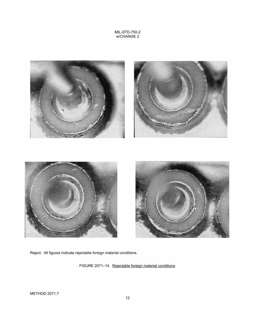
MIL-STD-750-2 w/CHANGE 2
METHOD 2071.7 12
Reject: All figures indicate rejectable foreign material conditions.
FIGURE 2071–14. Rejectable foreign material conditions.

MIL-STD-750-2 w/CHANGE 2
METHOD 2071.7 13
Reject: All figures indicate rejectable foreign material conditions.
FIGURE 2071–14. Rejectable foreign material conditions – Continued.

MIL-STD-750-2 w/CHANGE 2
METHOD 2071.7 14
Reject: All figures indicate rejectable foreign material conditions.
FIGURE 2071–14. Rejectable foreign material conditions – Continued.

MIL-STD-750-2 w/CHANGE 2
METHOD 2072.7 1 of 41
METHOD 2072.7
INTERNAL VISUAL TRANSISTOR (PRE–CAP) INSPECTION
1. Purpose. The purpose of this test method is to verify the construction and workmanship of bipolar transistors, field effect transistors (FET), discrete monolithic, multichip, and multijunction semiconductor devices excluding microwave and selected RF devices. The inspections of this test method will be performed prior to capping or encapsulation to detect those devices with internal defects that could lead to failures in normal application and verify compliance with the requirements of the applicable performance specification sheet.
2. Apparatus. The apparatus for this test method shall consist of the following.
a. Optical equipment capable of the specified magnifications. b. Light sources of sufficient intensity to adequately illuminate the devices being inspected. c. Adequate fixturing for handling the devices being inspected without causing damage. d. Adequate covered storage and transportation containers to protect devices from mechanical damage and
environmental contamination. e. Any visual standards (drawings and photographs) necessary to enable the inspector to make objective
decisions as to the acceptability of the devices being examined.
3. Definitions.
a. Active circuit area. All areas enclosed by the perimeter of functional circuit elements, operating metallization or any connected combinations thereof excluding beam leads.
b. Coupling (air) bridge. A raised layer of metallization used for interconnection that is isolated from the
surface of the element. c. Block resistor. A thin film resistor which for purposes of trimming is designed to be much wider than would
be dictated by power density requirements and shall be identified in the approved manufacturer's precap visual implementation document.
d. Contact via. The via where dielectric material is etched away in order to expose the Under Bump
Metallization (UBM) on the bond pads or solder bump attach pads. e. Channel. An area lying between the drain and the source of FET structures. f. Controlled environment. The controlled environment shall be class 1,000 or better in accordance with ISO
14644–1 and ISO 14644–2. The maximum allowable relative humidity shall not exceed 30 percent. g. Crazing. The presence of numerous minute cracks in the referenced material, (e.g., glassivation crazing). h. Detritus. Fragments of original or laser modified resistor material remaining in the kerf. i. Die coat. A thin layer of soft polyimide coating applied to the surface of a semiconductor element that is
intended to produce stress relief resulting from encapsulation and to protect the circuit from surface scratches.
j. Dielectric isolation. Electrical isolation of one or more elements of a semiconductor by surrounding the
elements with an isolating barrier such as semiconductor oxide.

MIL-STD-750-2 w/CHANGE 2
METHOD 2072.7 2
k. Dielectric layer or layers. Dielectric layer or layers deposited on the die surface to protect the redistribution
metallization, and to create the contact via for solder bump pad. l. Diffusion tub. A volume (or region) formed in a semiconductor material by a diffusion process (n- or p- type)
and isolated from the surrounding semiconductor material by a n–p or p–n junction or by a dielectric material (dielectric isolation, coplanar process, SOS, SOI).
m. Expanded contact. Design where the metal from the base and emitter contacts are expanded out to a larger
bond pad area that will fit a wire bond. n. Foreign material. Any material that is foreign to the semiconductor package, or any nonforeign material that
is displaced from its original or intended position within the package. o. Functional circuit elements. Diodes, transistors, crossunders, capacitors, and resistors. p. Gate oxide. The oxide or other dielectric that separates gate metallization (or other material used for the
gate electrode) from the channel of MOS structures. q. Glassivation. The top layer of transparent insulating material that covers the active circuit area metallization,
but excluding bonding pads. r. Glassivation cracks. Fissures in the glassivation layer. s. Junction line. The outer edge of a passivation step that delineates the boundary between "P" and "N" type
semiconductor material. An active junction is any P/N junction intended to conduct current during normal operation of the circuit element, (e.g., collector to base).
t. Kerf. That portion of the component area from which material has been removed or modified by trimming or
cutting. u. Line of separation. Visible distance or space between two features that are observed not to touch at the
magnification in use. v. Metal semiconductor field-effect transistor (MESFT). A field-effect transistor in which a metal semiconductor
rectifying contact is used for the gate electrode. Typically the structure is fabricated in gallium arsenide and the term GaAs MESFET may be used. Both depletion-type and enhancement type devices have been manufactured. The acronyms are D-MESFET, and E-MESFET, respectively.
w. Metallization nonadherence. Unintentional separation of material from an underlying substrate excluding air
bridges and undercutting by design. x. Multilayered metallization (conductors). Two or more layers of metal or any other material used for
interconnections that are not isolated from each other by insulating material. The term "underlying metal" shall refer to any layer below the top layer of metal.
y. Multilevel metallization (conductors). Two or more levels of metal or any other material used for
interconnections that are isolated from each other by insulating material (also referred to as interlevel dielectric).
z. Narrowest resistor width. The narrowest portion of a given resistor prior to trimming.

MIL-STD-750-2 w/CHANGE 2
METHOD 2072.7 3
aa. Non-expanded contact. Design where the metal of the bonding area is directly in contact with the base or
emitter areas. There is a direct contact from the wire bond to the silicon material. ab. Operating metallization (conductors). Metal or any other material used for interconnection except
metalized scribe lines, test patterns, unconnected functional circuit elements, unused bonding pads, and identification markings.
ac. Original width. The width dimension or distance that would have been present, in the absence of the
observed abnormality (e.g., original metal width, original diffusion width, original beam width, etc.). ad. Package post. A generic term used to describe the bonding location on the package. ae. Passivation. Silicon oxide, nitride, or other insulating material that is grown or deposited directly on the die
prior to the deposition of any metal. af. Passivation step. An abrupt change of elevation (level) of the passivation such as a contact window, or
operating metallization crossover. ag. Peripheral metal. All metal that lies immediately adjacent to or over the scribe grid. ah. Redistribution layer (RDL). Layer added to original wafer/die surface to allow for the redistribution of bond
pads into a format more suitable to flip chip. ai. Redistribution metallization. The metal deposited on the RDL to create the electrical conductors which
connect the original bond pads to the distributed solder bump pads. aj. Scribe grid. The area between the die where the sawing operation is performed. ak. Shooting metal. Metal (e.g., aluminum, gold) expulsion of various shapes and lengths from under the wire
bond at the bonding pad. al. Solder ball. Solder ball or sphere attached to a under bump metallization (UBM) package through the
contact via after a re-flow process. am. Solder bump. Solder that is either electroplated or screened into the photo resist opening. After the photo
resist is removed the solder resembles a bump before it is reflowed into ball or sphere. an. Substrate. The supporting structural material into or upon which or both the passivation, metallization and
circuit elements are placed. ao. Substrate via. A small hole formed through the wafer and metallized, causing electrical connection to be
made from the frontside (the side on which the circuitry is formed) to the backside of the wafer. ap. Thick film. That conductive/resistive/dielectric system that is a film having greater than 50,000Å thickness. aq. Thin film. That conductive/resistive/dielectric system that is a film equal to or less than 50,000Å in
thickness. ar. Under Bump Metallization (UBM). Metals deposited on top of the aluminum bond pads or on the solder
bump pads that enhance wetting and protect against intermetallic reactions between the solder and the original metal on the pads.
as. Via metallization. That which connects the metallization of one level to another. at. Wetting. The spreading, and sometimes absorption, of a liquid on or into a surface.
4. Procedure.
MIL-STD-750-2 w/CHANGE 2
METHOD 2072.7 4
4.1 General. The device shall be examined in a suitable sequence of observations within the specified magnification range to determine compliance with the requirements of the applicable specification sheet and the criteria of the specified test condition. If a specified visual inspection requirement is in conflict with the topology or construction of a specific device design, alternate inspection criteria may be included in the specification sheet. Any alternate inspection criteria contained in the specification sheet shall take precedence over the criteria of this test method. Any criteria of this test method intended for a specific device process or technology has been indicated. Where applicable, unused cells shall not be subjected to internal visual criteria.
a. Sequence of inspection. The order in which criteria are presented is not a required order of examination and may be varied at the discretion of the manufacturer. Visual criteria specified in 4.1.1, 4.1.2, 4.1.3, and 4.1.7, may be examined prior to die attachment with reexamination at low or high magnification after die attachment for these criteria. Visual criteria specified in 4.1.6.2 and 4.1.6.3 may be examined prior to lead wire bonding without reexamination after bonding.
b. Inspection control. Within the time interval between visual inspection and preparation for sealing, devices
shall be stored in a controlled environment (one which controls airborne particle count and relative humidity). The use of an inert gas environment, such as dry nitrogen shall satisfy the requirements for storing in a controlled environment. Devices examined in accordance with this test method shall be inspected and stored in a class 100,000 environment, in accordance with ISO 14644–1 and ISO 14644–2, except that the maximum allowable relative humidity shall not exceed 65 percent.
If devices are subjected to a high temperature bake (>+100C) immediately prior to sealing, the humidity control is not required. Unless a cleaning operation is performed prior to sealing, devices shall be in covered containers when transferred from one controlled environment to another.
c. Magnification. High magnification inspection shall be performed perpendicular to the die surface with a
bright field or incident light microscope with an internal illumination system. Low magnification inspection shall be performed with either a monocular, binocular, or stereo microscope, and the inspection performed within any appropriate angle, with the device under suitable illumination. The inspection criteria of 4.1.4 and 4.1.6.1 may be examined at high magnification at the manufacturer's option. High power magnification may be used to verify a discrepancy noted at a low power. All discrepancies found at low power magnification shall be considered discrepant. High power magnification cannot be used to overrule these discrepancies.
TABLE 2072–I. Die magnification requirements.
Chip size 1/ High magnification Low magnification
30 mils (0.76 mm) or less 100X to 200X 30X to 50X
31 to 60 mils (0.78 to 1.52 mm) 75X to 150X 30X to 50X
61 to 150 mils (1.55 to 3.81 mm) 35X to 120X 10X to 30X
Greater than 150 mils (3.81 mm) 25X to 75X 10X to 30X
1/ Length of shortest dimension.
d. Reinspection. Unless a specific magnification is required by the specification sheet, when inspection for product acceptance or quality verification of the visual requirements herein is conducted subsequent to the manufacturer's successful inspection, the additional inspection may be performed at any magnification specified herein. If sampling is used rather than 100 percent reinspection, reevaluation of lot quality in accordance with the reevaluation of lot quality of MIL–PRF–19500 shall be used.
e. Exclusions. If conditional exclusions have been allowed, specific instruction as to the location and
conditions for which the exclusion can be applied shall be documented in the assembly inspection drawing.

MIL-STD-750-2 w/CHANGE 2
METHOD 2072.7 5
4.1.1 Die metallization defects (high magnification). A die which exhibits any of the following defects shall be
rejected.
4.1.1.1 Metallization, scratches, probe marks and voids exposing underlying material (see figure 2072–1).
a. A scratch, probe mark or void that disturbs the innermost metallized guard ring (see figure 2072–2). b. Any die containing a void in the metallization at the bond pad window covering more than 25 percent of the
pad area. c. For devices with nonexpanded contacts and all power devices. Any scratch, probe mark or void, whether or
not underlying material is exposed, which isolates more than 25 percent of the total metallization of an active region from the bonding pad (see figure 2072–3).
d. For all devices with expanded contacts. A scratch, probe mark or void, whether or not underlying material is
exposed, which leaves less than 50 percent undisturbed metal width in the metal connecting the pad and contact regions (see figure 2072–4).
e. For expanded contacts with more than 10 contact regions. A scratch, probe mark or void extending across
more than 50 percent of the first half of any contact region (beginning at the bonding area) in more than 10 percent of the contact regions.
f. For expanded contacts with less than 10 contact regions. A scratch, probe mark or void in the contact area
which isolates more than 10 percent of the metalized contact from the bonding pad for any single contact area (contact finger) (see figure 2072–5).
FIGURE 2072–1. Metallization scratches, probe marks and voids (expanded contact).

MIL-STD-750-2 w/CHANGE 2
METHOD 2072.7 6
FIGURE 2072–2. Innermost guard band metallization scratches, probe marks and voids.
FIGURE 2072–3. Active region metallization scratches, probe marks and voids (nonexpanded contacts).
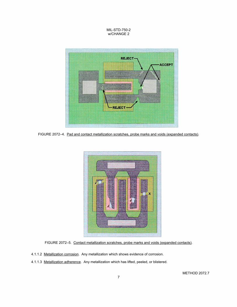
MIL-STD-750-2 w/CHANGE 2
METHOD 2072.7 7
FIGURE 2072–4. Pad and contact metallization scratches, probe marks and voids (expanded contacts).
FIGURE 2072–5. Contact metallization scratches, probe marks and voids (expanded contacts).
4.1.1.2 Metallization corrosion. Any metallization which shows evidence of corrosion.
4.1.1.3 Metallization adherence. Any metallization which has lifted, peeled, or blistered.

MIL-STD-750-2 w/CHANGE 2
METHOD 2072.7 8
4.1.1.4 Metallization probing. Criteria contained in 4.1.1.1 shall apply as limitations on probing damage (see figure 2072–6).
FIGURE 2072–6. Metallization probing damage.

MIL-STD-750-2 w/CHANGE 2
METHOD 2072.7 9
4.1.1.5 Metallization bridging. Metallization bridging between two normally unconnected metallization paths which reduces the separation, such that a line of oxide is not visible (no less than 0.1 mil (0.003 mm)) when viewed at the prescribed high magnification (see figures 2072–7 and 2072–8).
FIGURE 2072–7. Metallization bridging between two normally unconnected metallization areas.

MIL-STD-750-2 w/CHANGE 2
METHOD 2072.7 10
FIGURE 2072–8. Metallization bridging between two normally unconnected metallization paths.
4.1.1.6 Metallization alignment (see figures 2072–9 and 2072–10).
a. Except by design, contact window that has less than 50 percent of its area covered by continuous metallization.
b. A metallization path not intended to cover a contact window which is separated from the window by less
than 0.1 mil (0.003 mm). c. Except by design, any misalignment to the extent that continuous passivation color cannot be seen (i.e.,
metallization crossing passivation).
FIGURE 2072–9. Metallization misalignment, cross section view.

MIL-STD-750-2 w/CHANGE 2
METHOD 2072.7 11
FIGURE 2072–10. Metallization misalignment.
4.1.2 Passivation and diffusion faults (see figures 2072–11, 12, 13 and 14) (high magnification). A device which exhibits any of the following defects shall be rejected:
a. Any diffusion fault that allows bridging between any two diffused areas, any two metallization strips, or any
such combination not intended by design. b. Any passivation fault including pinholes not covered by glassivation that exposes semiconductor material
and allows bridging between any two diffused areas, any two metallization strips, or any such combination not intended by design.
c. Unless intended by design, a diffusion area which is discontinuous. d. Except by design, an absence of passivation visible at the edge and continuing under the metallization
causing an apparent short between the metal and the underlying material (closely spaced double or triple lines on the edges of the defect indicate that it may have sufficient depth to penetrate down to the silicon).
e. Except by design, any active junction not covered by passivation or glassivation. f. Unless by design, a contact window in a diffused area which extends across a junction.
MIL-STD-750-2 w/CHANGE 2
METHOD 2072.7 12
FIGURE 2072–11. Passivation and diffusion faults.

MIL-STD-750-2 w/CHANGE 2
METHOD 2072.7 13
FIGURE 2072–12. Passivation and diffusion faults, cross section view.
FIGURE 2072–13. Passivation and diffusion faults.

MIL-STD-750-2 w/CHANGE 2
METHOD 2072.7 14
FIGURE 2072–14. Contact window in a diffused area which extends across a junction faults.
4.1.3 Scribing and die defects (high magnification) (see figure 2072–15). A device which exhibits any of the following defects shall be rejected:
a. Unless by design, less than 0.1 mil (0.003 mm) passivation visible between active metallization or bond pad periphery and the edge of the die.
b. Any chip-out or crack in the active area. c. Except by design, die having attached portions of the active area of another die and which exceeds 10
percent of the area of the second die. d. Any crack which exceeds 2.0 mils (0.051 mm) in length inside the scribe grid or scribe line that points toward
active metallization or active area while extending into the oxide area. e. Any chip-out that extends to within 1.0 mil (0.025 mm) of a junction. f. Any crack or chip-out that extends under any active metallization area. g. Any crack chip-out which extends completely through the guard ring.

MIL-STD-750-2 w/CHANGE 2
METHOD 2072.7 15
FIGURE 2072–15. Die cracks and chips.

MIL-STD-750-2 w/CHANGE 2
METHOD 2072.7 16
4.1.4 Bond inspection (low magnification). This inspection and criteria shall be the required inspection for the bond type(s) and location(s) to which they are applicable when viewed from above (see figures 2072–16 and 2072–17). Wire tail is not considered part of the bond when determining physical bond dimensions. A device which exhibits any of the following defects shall be rejected.
4.1.4.1 Gold ball bonds.
a. Gold ball bonds on the die or package post where the ball bond diameter is less than 2.0 times or greater than 5.0 times the wire diameter (see figure 2072–18).
b. Gold ball bonds where the wire exit is not completely within the periphery of the ball (see figure 2072–19). c. Gold ball bonds where the exiting wire is not within the boundaries of the bonding pad (see figure 2072–20). d. Any visible intermetallic formation at the periphery of any gold ball bond (see figure 2072–21).

MIL-STD-750-2 w/CHANGE 2
METHOD 2072.7 17
NOTES: 1. 1.2.D ≤ W ≤ 5.0 D (width). 2. 0.5 D ≤ L ≤ 3.0 D (length).
Ultrasonic Thermocompression
NOTES: NOTES:
1. 1.2 D ≤ W ≤ 3.0 D (width). 1. 1.2 D ≤ W ≤ 3.0 D (width). 2. 1.5 D ≤ L ≤ 5.0 D (length). 2. 1.5 D ≤ L ≤ 5.0 D (length).
FIGURE 2072–16. Bond dimensions.
MIL-STD-750-2 w/CHANGE 2
METHOD 2072.7 18
FIGURE 2072–17. Lift and torn bonds.

MIL-STD-750-2 w/CHANGE 2
METHOD 2072.7 19
FIGURE 2072–18. Ball bond diameter is less than 2 times or greater than 5 times the wire diameter.
FIGURE 2072–19. Ball bonds where the wire exit is not completely within the periphery of the ball.
FIGURE 2072–20. Ball bonds where exiting wire is not within boundaries of the bonding pad.
MIL-STD-750-2 w/CHANGE 2
METHOD 2072.7 20
FIGURE 2072–21. Intermetallic formation at the periphery of gold ball bond.
4.1.4.2 Wedge bonds (see figure 2072–22).
a. Ultrasonic wedge bonds on the die or package post that are less than 1.2 times or greater than 3.0 times the wire diameter in width, or are less than 1.5 times or greater than 5.0 times the wire diameter in length.
b. Thermocompression wedge bonds on the die or package post that are less than 1.2 times or greater than
3.0 times the wire diameter in width or are less than 1.5 or greater than 5.0 times the wire diameter in length.
FIGURE 2072–22. Wedge bonds on the die or package post criteria.
MIL-STD-750-2 w/CHANGE 2
METHOD 2072.7 21
4.1.4.3 Tailless bonds (crescent) (see figure 2072–23).
a. Tailless bonds on the die or package post that are less than 1.2 times or greater than 5.0 times the wire diameter in width or are less than 0.5 times or greater than 3.0 times the wire diameter in length.
b. Tailless bonds where the bond impression does not cover the entire width of the wire.
FIGURE 2072–23. Tailless bond dimensions.
4.1.4.4 General (gold ball, wedge, and tailless).
a. Bonds on the die where less than 75 percent of the bond is within the unglassivated bonding pad area (except where due to geometry, the bonding pad is smaller than the bond, the criteria shall be 50 percent) (see figure 2072–24).
b. Wire bond tails that extend over and make contact with any metallization not covered by glassivation and not
connected to the wire (see figure 2072–25). c. Wire bond tails that exceed two wire diameters in length at the bonding pad or two wire diameters in length
at the package post (see figure 2072–26). d. Bonds on the package post that are not bonded entirely on the flat surface of the post top (see figure 2072–
27). e. A bond on top of another bond (see figure 2072–28). f. Bonds placed so that the separation between bonds and adjacent unglassivated die metallization is less
than 1.0 mil (0.025 mm) (see figure 2072–29). g. Bonds placed so that the separation between bonds and adjacent glassivated die metallization is less than
0.25 mil (0.006 mm) (see figure 2072–30). h. Bonds placed so that the separation between adjacent bonds is less than 0.25 mil (0.006 mm). This criteria
does not apply to designs which employ multiple bond wires in place of a single wire (see figure 2072–31). i. Bonds located where any of the bond is placed on an area containing die preform mounting material. j. Repair on conductors by bridging or addition of bonding wire or ribbon. k. For aluminum wires over 2.0 mils (0.051 mm) diameter, the bond width shall not be less than 1.0 times the
wire diameter.

MIL-STD-750-2 w/CHANGE 2
METHOD 2072.7 22
FIGURE 2072–24. Wire bond to bonding pad area misalignment.
FIGURE 2072–25. Wire bond tails contacting with metallization not covered by glassivation.

MIL-STD-750-2 w/CHANGE 2
METHOD 2072.7 23
FIGURE 2072–26. Wire bond tails limits.
FIGURE 2072–27. Bonds on the flat surface of the post top.

MIL-STD-750-2 w/CHANGE 2
METHOD 2072.7 24
FIGURE 2072–28. A bond on top of another bond.
FIGURE 2072–29. Bond to unglassivated die metallization.
MIL-STD-750-2 w/CHANGE 2
METHOD 2072.7 25
FIGURE 2072–30. Bond to glassivated die metallization.
FIGURE 2072–31. Adjacent bonds violating separation limits.

MIL-STD-750-2 w/CHANGE 2
METHOD 2072.7 26
4.1.5 Internal lead wires (low magnification). This inspection and criteria shall be required inspection for the location(s) to which they are applicable when viewed from above. A device which exhibits any of the following defects shall be rejected.
a. Any wire that comes closer than two wire diameters or 5 mils (0.127 mm), whichever is less, to unglassivated operating metallization, another wire (common wires and pigtails excluded) package post, unpassivated die area, or any portion of the package, including the plane of the lid to be attached (see figure 2072–32. (Within a 5.0 mil (0.127 mm) spherical radial distance from the perimeter of the bond on the die surface, the separation can be 1.0 mil (0.025 mm).)
b. Nicks, tears, bonds, cuts, crimps, scoring, or neckdown in any wire that reduces the wire diameter by more
than 25 percent (see figure 2072–33). c. Missing or extra lead wires. d. Bond lifting or tearing at interface of pad and wire (see figures 2072–17 and 2072–34). e. Any wire which runs from die bonding pad to package post and has no arc or stress relief (see
figure 2072–35). f. Except in common connectors, wires which cross other wires. g. Wire(s) not in accordance with bonding diagram. h. Wire is kinked (unintended sharp bend) with an interior angle of less than 90 degrees or twisted to an extent
that stress marks appear. i. Wire (ball bonded devices) not within 10 degrees of the perpendicular to the surface of the chip for a
distance of greater than 0.5 mil (0.013 mm) before bending toward the package post or other termination point (see figure 2072–36).
j. Excessive lead burn at lead post weld (see figure 2072–37). k. Pigtails must be less than the shortest distance required to bridge the narrowest unglassivated active metal
spacing (area between bond wire and bond pad) (see figure 2072–38). l. A bow or loop between double bonds at post greater than four times wire diameter (see figure 2072–39). m. Excessive loops, bows, or sags in any wire such that it could short to another wire, to another pad, to
another package post, to the die or touch any portion of the package (see figure 2072–40). n. When clips are used, solder fillets shall encompass at least 50 percent of the clip-to-die and post-to-clip
periphery. There shall be no deformation or plating defects on the clip.

MIL-STD-750-2 w/CHANGE 2
METHOD 2072.7 27
FIGURE 2072–32. Wire that violates allowed limits.
FIGURE 2072–33. Wire nicks, tears, bonds, cuts, crimps, scoring, or neckdown.

MIL-STD-750-2 w/CHANGE 2
METHOD 2072.7 28
FIGURE 2072–34. Bond tearing at interface of pad and wire.
FIGURE 2072–35. Wire that has no arc or stress relief.
FIGURE 2072–36. Wire not within 10 degrees of the perpendicular to the surface of the chip.

MIL-STD-750-2 w/CHANGE 2
METHOD 2072.7 29
FIGURE 2072–37. Excessive lead burn at lead post weld.
FIGURE 2072–38. Pigtail to unglassivated active metal spacing.
FIGURE 2072–39. Bow or loop in wire between double bonds at post.
FIGURE 2072–40. Excessive loops, bows, or sags in wire.

MIL-STD-750-2 w/CHANGE 2
METHOD 2072.7 30
4.1.6 Package conditions (magnification as indicated). A device which exhibits any of the following defects shall be rejected.
4.1.6.1 Conductive foreign material on die surface. All foreign material or particles may be blown off with a nominal gas blow (approximately 20 psi (138 kPa)) or removed with a soft camel hair, sable hair or stick pick brush. The device shall then be inspected for the following criteria (low magnification):
a. Non-embedded foreign particles (particles which are attached by less than one-half of their largest dimension) which are present on the surface of the die that are large enough to bridge the narrowest unglassivated active metal spacing (silicon chips shall be included as particles) (see figure 2072–41).
b. Glass-embedded foreign particles on the die that bridge two or more metallization paths or semiconductor
junctions, or any combination of metallization or junction (see figure 2072–42). c. Liquid droplets, chemical stains, or photoresist on the die surface. d. Except for unused cells, ink on the surface of the die that covers more than 25 percent of a bonding pad
area or that bridges any combination of unglassivated metallization or bare silicon areas (see figure 2072–43).
FIGURE 2072–41. Non-embedded foreign particles present on the surface of the die.

MIL-STD-750-2 w/CHANGE 2
METHOD 2072.7 31
FIGURE 2072–42. Glass-embedded foreign particles on the die that bridge paths or junctions.
FIGURE 2072–43. Ink on the surface of the die.

MIL-STD-750-2 w/CHANGE 2
METHOD 2072.7 32
4.1.6.2 Die mounting (low magnification).
a. Die mounting material buildup that extends onto the top surface of the die or extends vertically above the top surface of the die and interferes with bonding.
b. Die to header mounting material (wetting) which is not visible on the mounting surface of the package
around at least three complete sides or 75 percent of the die perimeter. Not applicable for eutectic bonded devices, as the bond occurs between the silicon and the gold rather than added braze fillet material, which results in no wetting around the sides of the die.) Adequate fillet is not required if the devices pass an approved thermal impedance test.
c. Any flaking of the die mounting material. d. Any balling of the die mounting material which does not exhibit a fillet when viewed from above (see figure
2072–44).
FIGURE 2072–44. Balling of the die mounting material.

MIL-STD-750-2 w/CHANGE 2
METHOD 2072.7 33
4.1.6.3 Die orientation (high magnification).
a. Die is not located or orientated in accordance with the applicable assembly drawing of the device. b. Die is visibly tipped or tilted (more than 10 degrees) with respect to the die attach surface (see figure
2072–45).
FIGURE 2072–45. Tipped or tilted die.

MIL-STD-750-2 w/CHANGE 2
METHOD 2072.7 34
4.1.6.4 Internal package defects (applicable to headers, bases, caps, and lids) (low magnification inspection). As an alternative to 100-percent visual inspection of lids and caps in accordance with the criteria of 4.1.6.1.a, the lids or caps may be subjected to a suitable cleaning process and quality verification procedure approved by the qualifying activity, provided the lids or caps are subsequently held in a controlled environment until capping or preparation for seal.
a. Any header or post-plating which is blistered, flaked, cracked, or any combination thereof. b. Any conductive particle which is attached by less than one-half of the longest dimension. c. A bubble, or a series of interconnecting bubbles, in the glass surrounding the pins which are more than
one-half the distance between the pin and body or pin-to-pin. d. Header posts which are severely bent. e. Any glass, die, or other material greater than 1.0 mil (0.025 mm) in its major dimension which adheres to the
flange or side of the header and would impair sealing. f. Any stain, varnish, or header discoloration which appears to extend under a die bond or wire bond. g. Any cracks in the header glass. h. For isolated stud packages:
(1) Any defect or abnormality causing the designed isolating paths between the metal island to be reduced
to less than 50 percent of the design separation. (2) A crack or chip-out in the substrate.
4.1.6.5 Presence of extraneous matter. Extraneous matter (foreign particles) shall include, but not be limited to:
a. Any foreign particle, loose or attached, greater than 3.0 mil (0.08 mm) or of any lesser size which is
sufficient to bridge nonconnected conducting elements of the device. b. Any wire tail extending beyond its normal end by more than two diameters at the semiconductor die pad or
by more than four wire diameters at the package post (see figure 2072–46). c. Any burr on a post (header lead) greater than 3.0 mil (0.08 mm) in its major dimension or of such
configuration that it may break away. d. Excessive semiconductor die bonding material buildup. A semiconductor die shall be mounted and bonded
so that it is not tilted more than 10 degrees from mounting surface. The bonding agent that accumulates around the perimeter of the semiconductor die and touches the side of the semiconductor die shall not accumulate to a thickness greater than that of the semiconductor die (see figures 2072–47 and 2072–48). Where the bonding agent is built up but is not touching the semiconductor die, the build up shall not be greater than twice the thickness of the semiconductor die. There shall be no excess semiconductor die bonding material in contact with the active surface of the semiconductor die, lead weld, feedthrough insulating material, any lead or post, or separated from the main bonding material area (see figure 2072–49). The die shall not touch or lay upon the lead weld, the feedthrough insulating material, or touch the post (see figure 2072–50).
e. Flaking on the header or posts or anywhere inside the case. f. Extraneous ball bonds anywhere inside case, except for attached bond residue when rebonding is allowed.

MIL-STD-750-2 w/CHANGE 2
METHOD 2072.7 35
FIGURE 2072–46. Acceptable and unacceptable voids and excessive pigtails.
MIL-STD-750-2 w/CHANGE 2
METHOD 2072.7 36
FIGURE 2072–47. Acceptable and unacceptable bonding material build-up.

MIL-STD-750-2 w/CHANGE 2
METHOD 2072.7 37
NOTE: Die and wire are not necessarily visible.
FIGURE 2072–48. Extraneous bonding material build-up.
MIL-STD-750-2 w/CHANGE 2
METHOD 2072.7 38
FIGURE 2072–49. Acceptable and unacceptable excess material.

MIL-STD-750-2 w/CHANGE 2
METHOD 2072.7 39
Figure 2072–50. Unacceptable die placement.
4.1.7 Glassivation and silicon nitride defects (high magnification). No device shall be acceptable that exhibits any of the following defects.
a. Glass crazing that prohibits the detection of visual criteria contained herein. b. Any glassivation which has delaminated. (Lifting or peeling of the glassivation may be excluded from the
criteria above, when it does not extend more than 1.0 mil (0.025 mm) distance from the designed periphery of the glassivation, provided that the only exposure of metal is adjacent to bond pads or of metallization leading from those pads.)
c. Except by design, two or more adjacent active metallization paths which are not covered by glassivation
(see figure 2072–51). d. Unglassivated areas at the edge of bonding pad which expose silicon (see figure 2072–52). e. Glassivation which covers more than 25 percent of the design bonding pad area (see figure 2072–53). f. Any cracking over an active die area.

MIL-STD-750-2 w/CHANGE 2
METHOD 2072.7 40
FIGURE 2072–51. Two or more adjacent active metallization paths not covered by glassivation.
FIGURE 2072–52. Unglassivated areas at the edge of bonding pad that expose silicon.

MIL-STD-750-2 w/CHANGE 2
METHOD 2072.7 41
FIGURE 2072–53. Glassivation covering the design bonding pad area.
4.2 Post organic protective coating visual inspection. If devices are to be coated with an organic protective coating, the devices shall be visually examined in accordance with the criteria specified in 4.1 prior to application of the coating. After the application and cure of the organic protective coating, the devices shall be visually examined under a minimum of 10X magnification. Devices which exhibit any of the following defects shall be rejected.
a. Except by design, any unglassivated or unpassivated areas or insulating substrate which has incomplete coverage.
b. Open bubbles, cracks, or voids in the organic protective coating. c. A bubble, or a chain of bubbles, which covers two adjacent metallized surfaces. d. Organic protective coating which has flaked or peeled. e. Organic protective coating which is tacky. f. Conductive particles which are embedded in the coating and are large enough to bridge the narrowest
unglassivated active metal spacing (silicon chips shall be included as conductive particles). g. A web of varnish (organic protective coating) that connects the wire with the header.
5. Summary. The following conditions shall be specified in the applicable performance specification sheet or
acquisition document: a. Test conditions, exceptions, or additions to the test method. b. Where applicable, any conflicts with approved circuit design topology or construction. c. Where applicable, gauges, drawings, and photographs that are to be used as standards for operator
comparison. d. When applicable, specific magnification.
MIL-STD-750-2 w/CHANGE 2
METHOD 2073.2 1 of 10
METHOD 2073.2
VISUAL INSPECTION FOR DIE (SEMICONDUCTOR DIODE)
1. Purpose. The purpose of this test method is to check the quality and workmanship of semiconductor die for compliance with the requirements of the individual specification sheet. All examinations and inspections shall be performed to detect and eliminate those die with defects that could lead to device failures. This test method will normally be used prior to installation on a 100 percent inspection basis. This test method may also be employed on a sampling basis prior to encapsulation to determine the effectiveness of the manufacturer's quality control and handling procedures.
2. Definitions. The following definitions shall apply: a. Active area: Any area where electrical contact may be made on the "N" or "P" regions of the die. b. Active region: Region covered by passivation that supports electrical activity and junction geometries. c. Foreign material (attached): Any conductive or nonconductive material that is not part of the die
construction. Conductive foreign material is defined as any substance that appears opaque under those conditions of lighting and magnification used in routine visual inspections. Therefore, nonconductive foreign material is defined as any substance that appears transparent
d. Junction: The boundary between "P" and "N" type semiconductor material. (In the case of a Schottky
diode, there is no actual junction other than the guard ring. Schottky diodes have a barrier that exists at the metal-silicon contact, however, for the purposes of this test method the barrier will be treated as a junction.)
e. Passivation: Silicon oxide, silicon nitride, or other insulating material that is grown or deposited directly over
the "P–N" junction or the Schottky guard ring "P–N" junction.
3. Apparatus.
a. The apparatus for this test shall include optical equipment and any visual standards (e.g., gauges, drawings, photographs) necessary to perform an effective examination and enable the examiner to make objective decisions on the acceptability of the die being examined. Adequate fixturing shall be provided for handling die without contamination during examination.
b. Unless otherwise specified by the individual specification sheet or procuring activity, the die magnifications
specified in table 2073–I shall be used for visual inspection. Visual inspection shall be performed with a monocular, binocular, or stereo microscope and shall be performed perpendicular to the die surface with normal incident illumination. The inspection shall be performed under suitable illumination. Binocular and stereo microscopes shall have each eyepiece individually focused for the examiner.
TABLE 2073–I. Magnification requirements.
Chip size High magnification Low magnification
30 mils (0.76 mm) or less 100X to 200X 30X to 50X
31 to 60 mils (0.78 to 1.52 mm) 75X to 150X 30X to 50X
61 to 150 mils (1.55 to 3.81 mm) 35X to 120X 20X to 30X
Greater than 150 mils (3.81 mm) 25X to 75X 20X to 30X

MIL-STD-750-2 w/CHANGE 2
METHOD 2073.2 2
4. Procedure. The die shall be examined in a suitable sequence of operations and at the specified magnifications to determine compliance with the requirements of the individual specification sheet and the criteria of the specified test conditions. The sequence of examinations required may be varied at the discretion of the manufacturer.
4.1 Die inspections. These inspections shall apply to alloy, diffused mesa, epitaxial mesa, planar, and epitaxial planar construction techniques. Unless otherwise specified, inspections shall be made on a random selection of at least one side of each die being inspected. If a lot fails, 100-percent inspection of the total lot shall be performed.
4.1.1 Type of die examined. Determine type of die being examined by referring to figure 2073–1 through figure 2073–8. An exact match is not necessary, select a representative figure. If a representative figure cannot be discerned, perhaps elements of different figures will apply. Contact the die vendor source for assistance in matching an appropriate figure. NOTE: Hexagonal shaped die will be inspected to the same criteria as square die.
a. Button contact diodes. figure 2073–1. b. High voltage planar diode I. figure 2073–2. c. High voltage planar diodes II. figure 2073–3. d. Inside moat mesa diodes. figure 2073–4. e. Low voltage contact overlay diodes. figure 2073–5. f. Low voltage planar diode. figure 2073–6. g. Outside moat mesa diodes. figure 2073–7. h. Schottky barrier diodes. figure 2073–8.
4.2 Examination options. Examine die according to the appropriate figure, its’ illustrations, and associated textual
criteria.
a. Option A: Front side visual inspection with sample size specified by individual specification sheet or procuring activity. If no sample size is specified, 100-percent visual is assumed.
b. Option B: Backside visual in addition to front side visual. Backside inspection is conducted with sample
size specified by individual specification sheet or procuring activity. If no sample size is specified, use sample size 22 for class H or sample size 45 for class K and reject on 1.
NOTE: If no option is specified by the individual performance specification sheet or procuring activity,
option A shall apply.
4.3 Foreign material. Examine die for attached conductive foreign material. No detailed illustration is provided for this due to the random nature of such material. The examiner is expected to use their own judgment in this matter.
4.4 Probe marks. Probe marks shall not penetrate the contact metal and expose any non-passivated active region.

MIL-STD-750-2 w/CHANGE 2
METHOD 2073.2 3
FIGURE 2073–1. Button contact diodes (metal button overlays junction and active area).
Note: Reject criteria
Edge chipping (D) may not extend more than 50 percent to metallization. Missing pieces (E) extending beyond 50 percent to junction boundary or additional attached pieces (F) defined by an incomplete cut or scribe line are not permitted. Additional front metallization extending 50 percent or more to the next geometric boundary (G) or pulled back to reveal contact area or any non-passivated active region. Cracks (H) must not extend near the metalized button closer than 50 percent and must not be directed toward button such that additional propagation would intersect the button.
Backside
Back contamination and foreign material (I), either firmly or loosely attached, exceeding 10 percent of total area. Missing backside metal (J) exceeding 20 percent of total area. Blisters (K) in metallization exceeding 10 percent of total area.

MIL-STD-750-2 w/CHANGE 2
METHOD 2073.2 4
FIGURE 2073–2. High voltage planar diode I (guard ring(s) and outside metal oxide edge cover or field plate).
Reject criteria
Smears (A), scratches (B) or probe marks (C) may not extrude metal such that it covers any guard rings.
Edge chipping or cracks (D) may not extend into outside metallization ring (or if absent, 50 percent of distance between chip edge and nearest active ring.)
Missing pieces (E) extending into outside metal ring or additional attached pieces (F) defined by an incomplete cut or scribe line are not permitted.
Additional front metallization extending over nearest ring boundary (G) or pulled back to reveal contact area or any non-passivated region.
Cracks (not illustrated) must not extend under the metalized areas and must not be present inside any of the active regions.
Backside
Backside contamination and foreign material (I), either firmly or loosely attached, exceeding 10 percent of total area. Missing backside metal (J) exceeding 20 percent of total area. Blisters (K) in metallization exceeding 10 percent of total area.

MIL-STD-750-2 w/CHANGE 2
METHOD 2073.2 5
FIGURE 2073–3. High voltage planar diodes II (integrated P-minus guard ring).
Reject criteria
Smears (A), scratches (B) or probe marks (C) may not extrude metal such that it extends over the next geometric boundary (covers the P-guard ring area). Edge chipping or cracks (D) may not extend into outside metallization ring (or if absent, 50 percent of distance between chip edge and active ring boundary.) Missing pieces (E) extending 50 percent of distance between chip edge and nearest ring boundary or additional attached pieces (F) defined by an incomplete cut or scribe line are not permitted. Additional front islands of metallization crossing any diffusion line (G1) or pulled back to reveal contact area or any non-passivated region (G2). Note that G2 does not apply to chips designed without requiring metal-passivation overlay. In this latter exception, much or all of the oxide window will be exposed as a legal part of the design. Cracks (not illustrated) must not extend under the metalized areas and must not be present inside any of the active regions.
Backside
Backside contamination and foreign material (I), either firmly or loosely attached, exceeding 10 percent of total area. Missing backside metal (J) exceeding 20 percent of total area. Blisters (K) in metallization exceeding 10 percent of total area.

MIL-STD-750-2 w/CHANGE 2
METHOD 2073.2 6
FIGURE 2073–4. Inside moat mesa diodes (passivated moat does not extent to edge of die).
Reject criteria
Smears (A), scratches (B) or probe marks (C) may not extrude metal outside metalized region over moat edge. Edge chipping or cracks (D) may not extend into moat area. Missing pieces (E) extending 50 percent of distance between chip edge and the moat or additional attached pieces (F) defined by an incomplete cut or scribe line are not permitted. Additional front metallization extending into the moat (G) or pulled back to reveal contact area or any non-passivated region Cracks (not illustrated) must not extend under the metalized areas nor more than 50 percent of the way across the moat from the outside.
Backside
Backside contamination and foreign material (I), either firmly or loosely attached, exceeding 10 percent of total area. Missing backside metal (J) exceeding 20 percent of total area. Blisters (K) in metallization exceeding 10 percent of total area.

MIL-STD-750-2 w/CHANGE 2
METHOD 2073.2 7
FIGURE 2073–5. Low voltage contact overlay diodes (metal overlays junction and active area field plate).
Reject criteria
Smears (A), scratches (B) or probe marks (C) may not extrude metal outside metalized region more than 50 percent of the way to the next boundary. Edge chipping (D) may not extend into metallization. Missing pieces (E) extending beyond 50 percent to metal boundary or additional attached pieces (F) defined by an incomplete cut or scribe are not permitted. Additional front metallization extending 50 percent or more to the next geometric boundary (G) or pulled back to reveal contact area or any non-passivated active region. Cracks (not illustrated) must not extend under the metalized areas and must not be present inside any of the active regions.
Backside
Backside contamination and foreign material (I), either firmly or loosely attached, exceeding 10 percent of total area. Missing backside metal (J) exceeding 20 percent of total area. Blisters (K) in metallization exceeding 10 percent of total area.

MIL-STD-750-2 w/CHANGE 2
METHOD 2073.2 8
FIGURE 2073–6. Low voltage planar diode.
Reject criteria
Smears (A), scratches (B) or probe marks (C) may not extrude metal outside junction boundary region. Edge chipping or cracks (D) may not extend beyond 50 percent between chip edge and junction boundary. Missing pieces (E) extending beyond 50 percent to junction boundary or additional attached pieces (F) defined by an incomplete cut or scribe line are not permitted. Additional front islands of metallization crossing any diffusion line (G1) or pulled back to reveal contact area or any non-passivated region (G2). Note that G2 does not apply to chips designed without requiring metal passivation overlay. In this latter exception, much or all of the oxide window will be exposed as a legal part of the design. Cracks (not illustrated) must not extend under the metalized areas and must not be present inside any of the active regions. Sharp corner usually denotes non-active regions
Backside
Backside contamination and foreign material (I), either firmly or loosely attached, exceeding 10 percent of total area. Missing backside metal (J) exceeding 20 percent of total area. Blisters (K) in metallization exceeding 10 percent of total area.

MIL-STD-750-2 w/CHANGE 2
METHOD 2073.2 9
FIGURE 2073–7. Outside moat mesa diodes (moat extends from mesa to edge of die).
Reject criteria
Smears (A), scratches (B) or probe marks (C) may not extrude metal outside metalized region over moat edge. Edge chipping (D) may not extend into moat area more than 50 percent. Missing pieces (E) extending beyond 50 percent across moat or additional attached pieces (F) defined by an incomplete cut or scribe line are not permitted. Additional front metallization extending over into the moat (G) or missing front metal (H) exceeding 5 percent of total mesa area. Cracks (not illustrated) must not extend under the metalized area no more than 50 percent of the way across the moat from the outside
Backside
Backside contamination and foreign material (I), either firmly or loosely attached, exceeding 10 percent of total area. Missing backside metal (J) exceeding 15 percent of total area. Blisters (K) in metallization exceeding 10 percent of total area.

MIL-STD-750-2 w/CHANGE 2
METHOD 2073.2 10
FIGURE 2073–8. Schottky barrier diodes (metal overlays barrier edge and active area field plate).
Reject criteria
Smears (A), scratches (B) or probe marks (C) may not extrude metal outside metalized region more than 50 percent to the next geometric boundary. Edge chipping (D) may not extend into metallization. Missing pieces (E) extending more than 50 percent of distance from chip edge and metallization or additional attached pieces (F) that exceed chip dimensional specifications are not permitted. Additional front metallization extending 50 percent or more to the next geometric boundary (G) or pulled back to reveal contact area or any non-passivated barrier region. Cracks (not illustrated) must not extend under the metalized areas and must not be present inside any of the active regions.
Backside
Backside contamination and foreign material (I), either firmly or loosely attached, exceeding 10 percent of total area. Missing backside metal (J) exceeding 20 percent of total area. Blisters (K) in metallization exceeding 10 percent of total area.

MIL-STD-750-2 w/CHANGE 2
METHOD 2074.6 1 of 37
METHOD 2074.6
INTERNAL VISUAL INSPECTION (DISCRETE SEMICONDUCTOR DIODES)
1. Purpose. The purpose of this test method is to check the materials, design, construction, and workmanship of discrete semiconductor diodes and other two-terminal semiconductor devices described herein. All examinations and inspections shall be performed to detect and eliminate those devices with defects that could lead to device failures. Opaque glass type construction devices shall be examined before encapsulation. (After encapsulation, see test method 2068 of this standard). Metal can devices shall be examined before capping. (After capping or sealing, see test method 2071 of this standard). Clear glass construction devices shall be examined after encapsulation.
2. Apparatus.
a. The apparatus for these inspections shall include optical equipment and any visual standards (e.g., gauges, drawings, photographs) necessary to perform an effective examination and enable the operator to make objective decisions on the acceptability of the device being examined. Any necessary fixturing for handling devices during examination to promote efficient operation without damaging the units shall be provided.
b. A monocular, binocular, or stereo microscope capable of magnification from 20X minimum to 30X maximum,
shall be used unless otherwise specified. The inspection shall be performed under suitable illumination.
3. Procedure. The devices shall be examined at the specified magnifications to determine compliance with the requirements of the applicable sections of this test method based on device construction. Examinations for transparent body devices may be performed anytime prior to body coating or painting. Axial construction devices shall be viewed at approximate right angles to their major axis while being rotated through 360 degrees. For the time interval, if any, between visual inspection and package sealing, devices shall be stored, handled, and processed in a manner to avoid contamination and to preserve the integrity of the devices as inspected.
3.1 Die criteria (applicable to all body styles).
a. Chip outs (see figure 2074–1). Reject for chip outs that extend more than 50 percent of the way up the moat area (mesa devices) or that extend to within 2.0 mils (0.051 mm) of the junction.
NOTE: Actual junction location will vary depending on specific device characteristics.
Accept: Chipouts ≤ 50 percent up moat and ≥ 2 mils (0.051 mm) from junction – "A" Accept: Chipouts ≥ 2 mils (0.051 mm) from junction – "B" Reject: Chipouts ≤ 2 mils (0.051 mm) from junction – "C"
FIGURE 2074–1. Die chip outs.

MIL-STD-750-2 w/CHANGE 2
METHOD 2074.6 2
b. Cracks (see figure 2074–2). Reject for cracks that extend to within 2.0 mils (0.051 mm) of the junction or
propagate in the direction of the junction. NOTE: The junction may be in a different place than shown depending on specific device characteristics.
Reject: Cracks ≤ 2 mils (0.051 mm) from junction or propagating toward junction – "A" Accept: Cracks ≥ 2 mils (0.051 mm) from junction and propagating away from junction – "B"
FIGURE 2074–2. Die cracks.
3.2 Applicable body styles. The devices shall be examined in accordance with the following appendixes as applicable for the body style involved.
Appendix A: Axial lead, transparent body, pressure contact design. Appendix B: Axial lead, transparent body, straight through lead to die contact. Appendix C: Axial lead and surface mount, double plug, transparent body (dumet plug, round end-cap,
soft glass). Appendix D: Axial lead and surface mount, double plug, transparent body (tungsten or molybdenum plug,
square end-cap, hard glass). Appendix E: Axial lead, transparent body, point contact. Appendix F: Axial lead, double plug, opaque body, power rectifier and regulator. Appendix G: Metal body, axial lead, solder contact design. Appendix H: Metal body, stud mounted, solder contact design. Appendix I: Metal body, diamond base regulators, solder contact design.
4. Summary. The following conditions shall be specified in the applicable performance specification sheet or acquisition document:
a. Detailed requirements for materials, design, construction, and workmanship. b. Magnification requirements, if other than specified herein.

MIL-STD-750-2 w/CHANGE 2
METHOD 2074.6 3
APPENDIX A
AXIAL LEAD, TRANSPARENT BODY, PRESSURE CONTACT DESIGN
A.1 General. The following examinations shall be made after encapsulation (C and S bend whisker). This appendix is a mandatory part of this test method. The information contained herein is intended for compliance.
A.1.1 Glass cracks and chips (see figure 2074–A1). No cracks shall be allowed in the vicinity of the cavity. Any crack originating at either end of the package or crack that extends into the body of the glass toward the cavity more than 25 percent of the glass-to-glass or glass-to-metal seal length shall be cause for rejection. Any glass chip deep enough to expose the plug or lead surface and extending longitudinally into the glass-to-metal seal toward the cavity to reduce the effective seal length to less than one external lead diameter shall be cause for rejection.
A.1.2 Incomplete seal. All devices shall be inspected for glass-to-metal seal or glass-to-glass seal. Both seals shall be a minimum of one external lead diameter over the entire sealed portion (sealed interface).
A.1.3 Bubbles in seal. All devices shall be inspected for bubbles in the glass-to-metal or glass-to-glass seal. A series of bubbles that reduce the effective seal length to less than one external lead diameter shall be cause for rejection. Bubbles in the glass, but not affecting the glass-to-glass or glass-to-metal seal area, are not cause for rejection.
A.1.4 Glass package deformities (see figure 2074–A2). Any glass envelope deformity equal to or greater than 75 percent of the external lead diameter shall be cause for rejection.
A.1.5 Extraneous matter. A device shall be rejected if there are unattached solder balls, semiconductor material, chips, flaked plating, or opaque material that is larger than the smallest distance between exposed active areas.
FIGURE 2074–A1. Glass cracks and chips.

MIL-STD-750-2 w/CHANGE 2
METHOD 2074.6 4
APPENDIX A
FIGURE 2074–A2. Package deformities.

MIL-STD-750-2 w/CHANGE 2
METHOD 2074.6 5
APPENDIX A
A.1.6 Solder protrusions (see figure 2074–A3). All devices shall be inspected for solder protrusions. Any device with a protrusion that extends more than twice the smallest protrusion width shall be rejected.
FIGURE 2074–A3. Solder protrusions.
A.1.7 Pressure contact defects. The following misalignments or deformations shall be cause for rejection:
a. Whisker embedded within glass body wall (see figure 2074–A4).
FIGURE 2074–A4. Embedded whisker.

MIL-STD-750-2 w/CHANGE 2
METHOD 2074.6 6
APPENDIX A
b. Toe contact between base of C or S bend whisker and top surface of die caused by insufficient loading (see figure 2074–A5).
FIGURE 2074–A5. Whisker toe contact.
c. Toe contact on top surface of die (see figure 2074–A6).
FIGURE 2074–A6. Whisker toe contact on top surface of die.

MIL-STD-750-2 w/CHANGE 2
METHOD 2074.6 7
APPENDIX A
d. Heel contact between base of C or S bend whisker and top surface of die (see figure 2074–A7).
FIGURE 2074–A7. Whisker heel contact.
e. Point contact between base of C or S bend whisker and top surface of die except by design (deformed or twisted whisker) (see figure 2074–A8).
FIGURE 2074–A8. Whisker point contact.

MIL-STD-750-2 w/CHANGE 2
METHOD 2074.6 8
APPENDIX A
f. Design compressed height (see figures 2074–A9 and 2074–10). Either half of an S or a C bend whisker that is compressed so that any dimension is reduced to less than 50 percent of its design shall be rejected.
FIGURE 2074–A9. S bend whisker compressed height.
FIGURE 2074–A10. C bend whisker compressed height.

MIL-STD-750-2 w/CHANGE 2
METHOD 2074.6 9
APPENDIX A
A.1.8 Whisker weld to post. Any device that exhibits weld splash or splatter (teardrop or balled) between whisker and post shall be rejected when it exceeds 25 percent of nominal lead diameter. The profile of the whisker weld to post shall not allow light penetration by more than 50 percent of lead diameter when using back lighting techniques.
A.1.9 Die-to-post or die-to-die contact area. Solder shall not be rough in appearance and shall be fused to a minimum of one-half the available bonding perimeter. Any solder overflow that touches the opposite surface of the die or dice shall be cause for rejection.
A.1.10 Die alignment (see figure 2074–A11). A device shall be rejected if the die surface is not within 15 degrees of being normal to the centerline of the mounting post.
FIGURE 2074–A11. Die alignment.
A.1.11 Lead alignment defects (applicable to that portion of each lead within the glass envelope). A device lead which is either misaligned or bent so that it makes an angle with the principle device axis greater than 10 degrees shall be rejected.
A.1.12 Multiple chip attachment defects. A multiple chip stack that tilts more than 10 degrees from the principle axis of the device shall be cause for rejection.

MIL-STD-750-2 w/CHANGE 2
METHOD 2074.6 10
APPENDIX B
AXIAL LEAD, TRANSPARENT BODY, STRAIGHT THROUGH LEAD TO DIE CONTACT
B.1 General. The following criteria shall be specified for the straight through construction (see figure 2074–B1) after encapsulation but before body coating or painting. This appendix is a mandatory part of this test method. The information contained herein is intended for compliance.
B.1.1 Glass cracks and chips (see figure 2074–A1). No cracks shall be allowed in the vicinity of the cavity. Any crack originating at either end of the package or crack that extends into the body of the glass toward the cavity more than 25 percent of the glass-to-glass or glass-to-metal seal length shall be cause for rejection. Any glass chip deep enough to expose the plug or lead surface and extending longitudinally into the glass-to-metal seal toward the cavity to reduce the effective seal length to less than one external lead diameter shall be cause for rejection.
B.1.2 Incomplete seal. All devices shall be inspected for glass-to-metal seal or glass-to-glass seal. Both seals shall be a minimum of one external lead diameter over the entire sealed portion (sealed interface).
B.1.3 Bubbles in seal. All devices shall be inspected for bubbles in the glass-to-metal or glass-to-glass seal. A series of bubbles that reduce the effective seal length to less than one external lead diameter shall be cause for rejection. Bubbles in the glass, but not affecting the glass-to-glass or glass-to-metal seal area, are not cause for rejection.
B.1.4 Glass package deformities (see figure 2074–A2). Any glass envelope deformity equal to or greater than 75 percent of the external lead diameter shall be cause for rejection.
FIGURE 2074–B1. Straight through internal construction.
MIL-STD-750-2 w/CHANGE 2
METHOD 2074.6 11
APPENDIX B
B.1.5 Extraneous matter. A device shall be rejected if there are unattached solder balls, semiconductor material, chips, flaked plating, or opaque material that is larger than the smallest distance between exposed active areas.
B.1.6 Die to post solder connection.
a. Solder voids (see figure 2074–B2). A device shall be rejected if solder flow is less than 50 percent of the perimeter of the minimum available contact area of the post.
FIGURE 2074–B2. Solder voids.
b. Solder overflow (see figure 2074–B3). A device shall be rejected if any solder flow touches the opposite surface of the die.
FIGURE 2074–B3. Solder bridge.

MIL-STD-750-2 w/CHANGE 2
METHOD 2074.6 12
APPENDIX B
B.1.7 Lead to die solder connection (see figure 2074–B4). A device shall be rejected if more than 50 percent of the perimeter of the available contact area of the lead is void of solder.
FIGURE 2074–B4. Solder voids.
a. Solder overflow (see figure 2074–B5). A device shall be rejected if solder flow extends beyond 50 percent of the distance from the metal to the outer edge of the oxide.
FIGURE 2074–B5. Solder overflow.

MIL-STD-750-2 w/CHANGE 2
METHOD 2074.6 13
APPENDIX B
b. Solder protrusion, slivers, and spikes (see figure 2074–B6). A device shall be rejected if solder slivers and spikes are not securely attached to the main body. A securely attached sliver of spike is one having a cross sectional area greater at the area of attachment than anywhere else on the solder protrusion and having no necked down areas. Solder protrusions, slivers, and spikes whose length exceeds twice the smallest width of attachment shall be rejected.
FIGURE 2074–B6. Solder slivers and spikes.
c. Solder balls. A device shall be rejected if there are any insecurely attached solder balls. An insecurely
attached solder ball is one whose major cross sectional area is more than twice the cross sectional area of the attachment.
B.1.8 Die-to-die solder connection (see figure 2074–B7). A device shall be rejected if more than 50 percent of the
perimeter of the available contact area of the die is void of solder.
FIGURE 2074–B7. Die-to-die solder connection.

MIL-STD-750-2 w/CHANGE 2
METHOD 2074.6 14
APPENDIX C
AXIAL LEAD AND SURFACE MOUNT, DOUBLE PLUG, TRANSPARENT BODY (DUMET PLUG, ROUND END-CAP, SOFT GLASS)
C.1 General. This appendix is a mandatory part of this test method. The information contained herein is intended for compliance.
C.1.1 Glass cracking (see figure 2074–C1). Spiral or longitudinal cracks of any length originating at either end that propagate in the direction of the die are cause for rejection. Reject for cracks that are not confined to the glass surface or the outer 25 percent of the seal length. Small surface impact marks, "c" cracks, and microcracks are acceptable if they are confined to the glass surface with no other cracks radiating from them. Cracks confined to the outer 25 percent of the designed seal length that propagate back toward the starting edge (away from the die area) are acceptable.
FIGURE 2074–C1. Glass cracks.

MIL-STD-750-2 w/CHANGE 2
METHOD 2074.6 15
APPENDIX C
C.1.2 High seal (see figure 2074–C2). Any device which displays a glass case off center condition reducing the seal band of either plug by more than 25 percent of its designed length shall be cause for rejection.
FIGURE 2074–C2. High seal.

MIL-STD-750-2 w/CHANGE 2
METHOD 2074.6 16
APPENDIX C
C.1.3 Insufficient seal (see figure 2074–C3). Any anomaly such as bubbles, plug blisters, separations, leaching, or undersealing that affects the combined seal length of either plug by reducing the a sealing band to less than 50 percent of the designed seal length on any package type shall be cause for rejection.
FIGURE 2074–C3. Insufficient seal.

MIL-STD-750-2 w/CHANGE 2
METHOD 2074.6 17
APPENDIX C
C.1.4 Plug alignment and displacement (see figure 2074–C4 and 2074–C5). All devices shall be inspected for proper plug alignment. A plug displacement distance more than 25 percent of the diameter of the plug shall be cause for rejection. The plug shall not tilt to the degree that it touches the chip or is misaligned from the other plug axis more than 5 degrees.
FIGURE 2074–C4. Plug alignment.
FIGURE 2074–C5. Plug displacement.
C.1.5 Extraneous matter. A device shall be rejected if there are unattached solder balls, semiconductor material, chips, flaked plating, or opaque material that is larger than the smallest distance between exposed active areas (die cavity area). Extraneous materials between the glass seal and the slug is considered attached and shall not be cause for rejection.
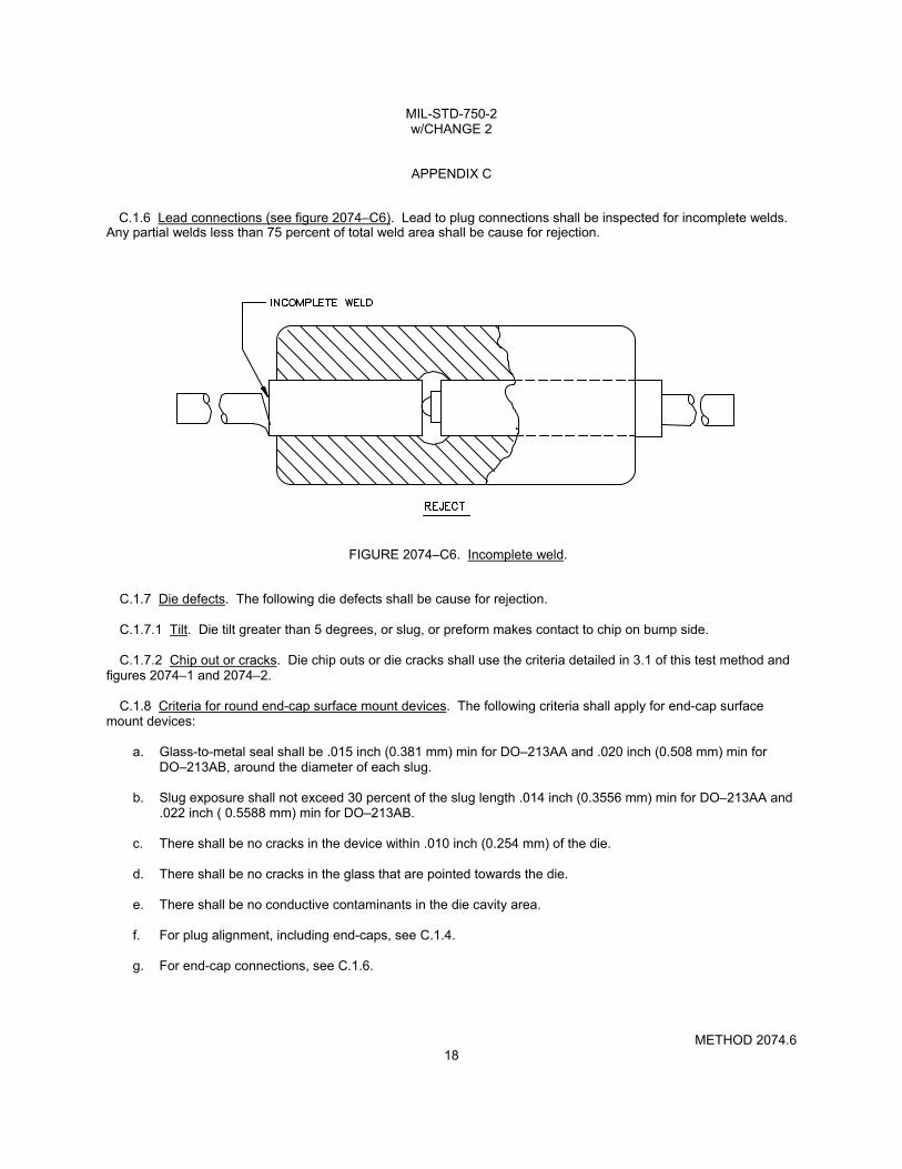
MIL-STD-750-2 w/CHANGE 2
METHOD 2074.6 18
APPENDIX C
C.1.6 Lead connections (see figure 2074–C6). Lead to plug connections shall be inspected for incomplete welds. Any partial welds less than 75 percent of total weld area shall be cause for rejection.
FIGURE 2074–C6. Incomplete weld.
C.1.7 Die defects. The following die defects shall be cause for rejection.
C.1.7.1 Tilt. Die tilt greater than 5 degrees, or slug, or preform makes contact to chip on bump side.
C.1.7.2 Chip out or cracks. Die chip outs or die cracks shall use the criteria detailed in 3.1 of this test method and figures 2074–1 and 2074–2.
C.1.8 Criteria for round end-cap surface mount devices. The following criteria shall apply for end-cap surface mount devices:
a. Glass-to-metal seal shall be .015 inch (0.381 mm) min for DO–213AA and .020 inch (0.508 mm) min for DO–213AB, around the diameter of each slug.
b. Slug exposure shall not exceed 30 percent of the slug length .014 inch (0.3556 mm) min for DO–213AA and
.022 inch ( 0.5588 mm) min for DO–213AB. c. There shall be no cracks in the device within .010 inch (0.254 mm) of the die. d. There shall be no cracks in the glass that are pointed towards the die. e. There shall be no conductive contaminants in the die cavity area. f. For plug alignment, including end-caps, see C.1.4. g. For end-cap connections, see C.1.6.

MIL-STD-750-2 w/CHANGE 2
METHOD 2074.6 19
APPENDIX D
AXIAL LEAD AND SURFACE MOUNT, DOUBLE PLUG, TRANSPARENT BODY (TUNGSTEN OR MOLYBDENUM PLUG, SQUARE END-CAP, HARD GLASS).
D.1 General. This appendix is a mandatory part of this test method. The information contained herein is intended for compliance.
D.1.1 Glass.
a. Cracks. No cracks allowed except cracks confined to the outer 25 percent of the designed seal length that propagate back toward the starting edge (away from the die area) are acceptable. Small surface impact marks, "c" cracks, and microcracks are acceptable if they are confined to the glass surface with no other cracks radiating from them.
b. Chip outs (see figure 2074–D1). Edge chip outs that expose a plug and are not confined to the outer 25
percent of the designed seal length are cause for rejection. Edge chip outs (regardless of size) that expose a plug and create a sharp angle or "V" shape that points toward the die area are rejects.
FIGURE 2074–D1. Chip outs.
c. Holes. Any hole over the die or slug area greater that 50 percent of the glass thickness in depth is cause for rejection, except that holes of any depth are acceptable in the outer 25 percent of the designed seal length.
d. Deformities (see figure 2074–D2). Any glass surface deformity that causes the glass surface to be
displaced by more than 10 percent of the designed glass diameter, or that results in the device not meeting a dimensional requirement, is cause for rejection.
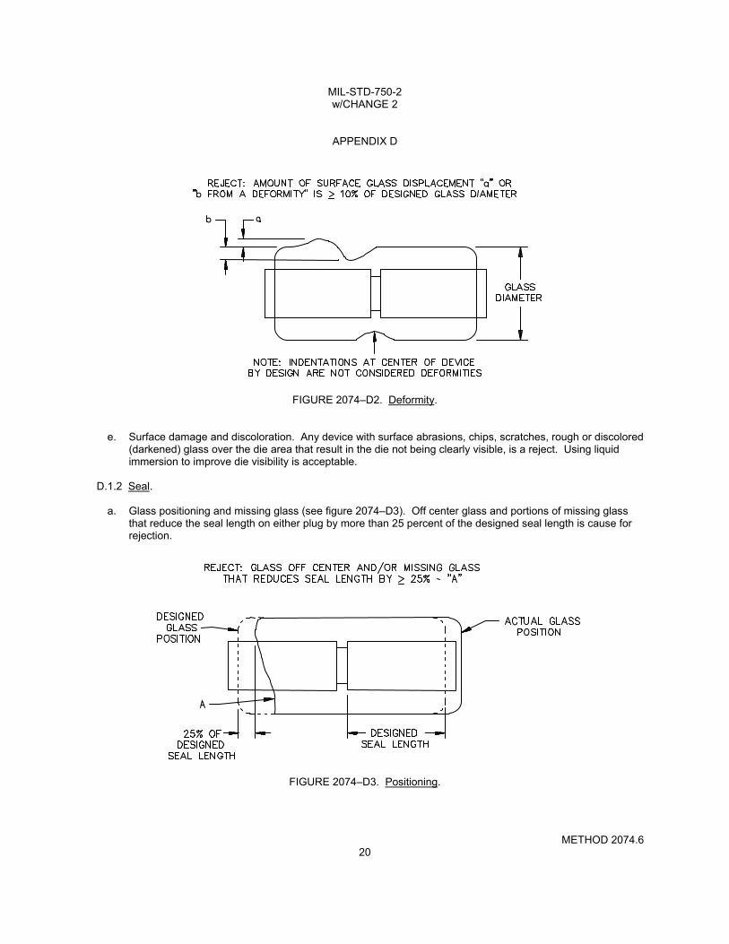
MIL-STD-750-2 w/CHANGE 2
METHOD 2074.6 20
APPENDIX D
FIGURE 2074–D2. Deformity.
e. Surface damage and discoloration. Any device with surface abrasions, chips, scratches, rough or discolored (darkened) glass over the die area that result in the die not being clearly visible, is a reject. Using liquid immersion to improve die visibility is acceptable.
D.1.2 Seal.
a. Glass positioning and missing glass (see figure 2074–D3). Off center glass and portions of missing glass
that reduce the seal length on either plug by more than 25 percent of the designed seal length is cause for rejection.
FIGURE 2074–D3. Positioning.

MIL-STD-750-2 w/CHANGE 2
METHOD 2074.6 21
APPENDIX D
b. Insufficient seal (see figure 2074–D4). Seal surface anomalies such as undercut, separations, plug blisters, scratches or cracks, bubbles, silicon chips, fibers, or missing plating which, when combined, reduce the sealing length along any linear path to less than 50 percent of the designed seal length are cause for rejection.
NOTE: Lines or "strings" of small bubbles are considered to be seal anomalies for the entire length of
the line.
FIGURE 2074–D4. Insufficient seal.
c. Extraneous materials. A device shall be rejected if there are unattached solder balls, semiconductor material, chips, flaked plating, or opaque material that is larger than the smallest distance between exposed active areas (die cavity area). Extraneous materials between the glass seal and the slug are considered attached and shall not be cause for rejection.
D.1.3 Alignment. NOTE: Any die to plug non-contact that occurs as a result of die or plug misalignment is most
accurately evaluated by thermal impedance testing. In cases where pass/fail status of a device is unclear based on the alignment requirements presented herein, thermal impedance testing may be used to determine the acceptability of the device.
a. Die alignment. Any die that tilts more than 5 degrees with respect to the surface of either plug or that tilts sufficiently to make any unintended contact with the plug is cause for rejection (see figure 2074–D5). Any die that is out of axial alignment such that it extends beyond the slug more than 20 percent of it length or width is cause for rejection (see figure 2074–D6).
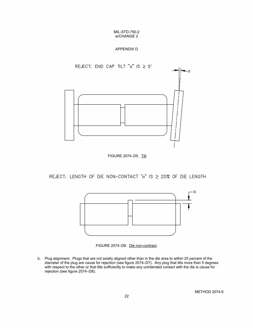
MIL-STD-750-2 w/CHANGE 2
METHOD 2074.6 22
APPENDIX D
FIGURE 2074–D5. Tilt.
FIGURE 2074–D6. Die non-contract.
b. Plug alignment. Plugs that are not axially aligned other than in the die area to within 25 percent of the diameter of the plug are cause for rejection (see figure 2074–D7). Any plug that tilts more than 5 degrees with respect to the other or that tilts sufficiently to make any unintended contact with the die is cause for rejection (see figure 2074–D8).
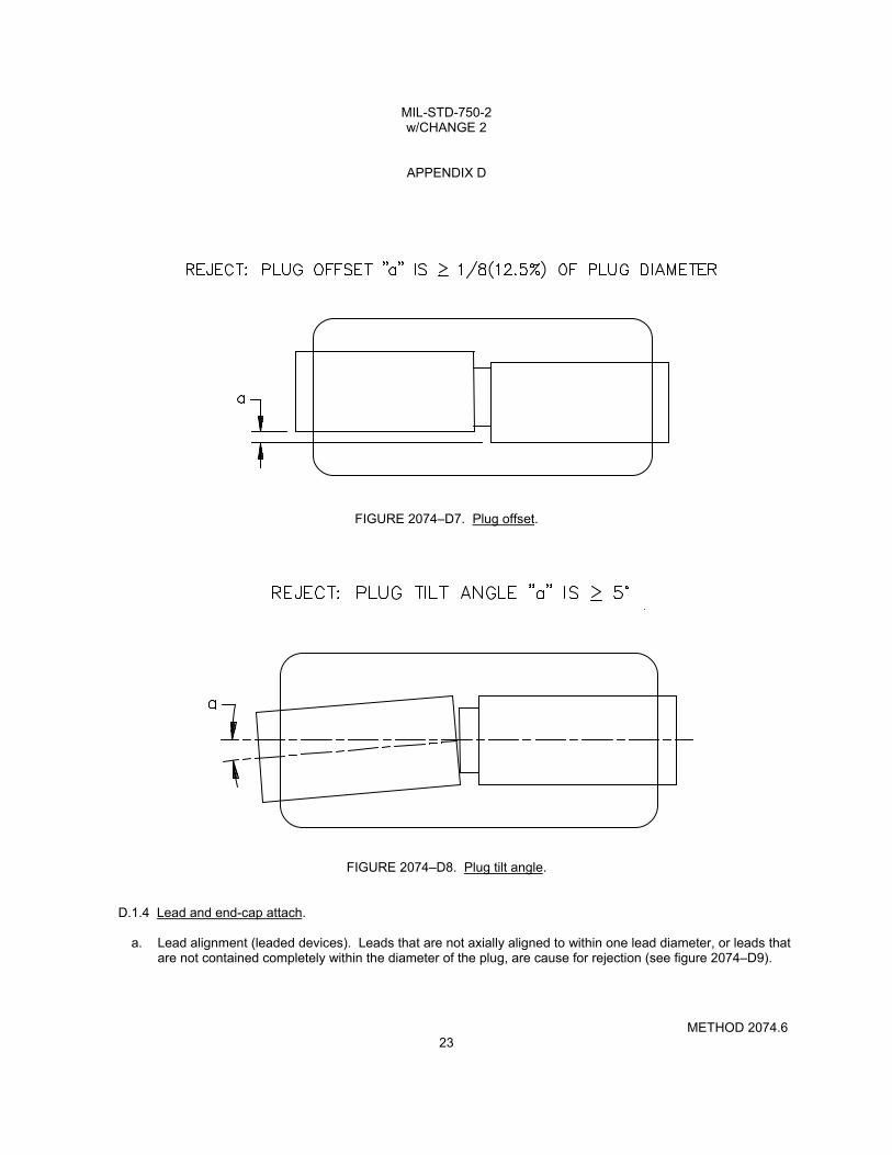
MIL-STD-750-2 w/CHANGE 2
METHOD 2074.6 23
APPENDIX D
FIGURE 2074–D7. Plug offset.
FIGURE 2074–D8. Plug tilt angle.
D.1.4 Lead and end-cap attach.
a. Lead alignment (leaded devices). Leads that are not axially aligned to within one lead diameter, or leads that are not contained completely within the diameter of the plug, are cause for rejection (see figure 2074–D9).

MIL-STD-750-2 w/CHANGE 2
METHOD 2074.6 24
APPENDIX D
FIGURE 2074–D9. Lead offset.
b. Braze. Terminals that are not brazed to the plug around at least 90 percent of the terminal perimeter are cause for rejection. Any cracks or fissures in the braze are cause for rejection. Pin holes in the braze are acceptable.
c. End-caps (surface mount). Reject for end-caps that do not allow at least 3.0 mils (0.076 mm) clearance
from the glass body to the mounting surface on all four sides (see figure 2074–D10). Reject for end-caps that are not perpendicular to the plugs to within 5 degrees (see figure 2074–D11). Reject for end-caps that are bent sufficiently to cause the device to exceed any specified diode or end-cap dimension (see figure 2074–D12). Reject for end-cap rotation where mounting surfaces are not co-planer to each other to within 5 degrees (see figure 2074–D13). Reject for tabs that have indentations, holes, or other damage affecting more than 25 percent of any mounting surface (see figure 2074–D14). Reject for end-caps that exhibit flaking, blistering, or peeling.
FIGURE 2074–D10. End-cap clearance.

MIL-STD-750-2 w/CHANGE 2
METHOD 2074.6 25
APPENDIX D
FIGURE 2074–D11. End-cap tilt.
FIGURE 2074–D12. End-cap deformation.

MIL-STD-750-2 w/CHANGE 2
METHOD 2074.6 26
APPENDIX D
FIGURE 2074–D13. End-cap rotation.
FIGURE 2074–D14. Mounting surface nicks and pits.
MIL-STD-750-2 w/CHANGE 2
METHOD 2074.6 27
APPENDIX D
D.1.5 Die effects.
a. Chip outs or cracks. Die chip outs or die cracks shall use the criteria detailed in paragraph 3.1 of this test method and figures 2074–1 and 2074–2.
b. Conductive contaminants. There shall be no conductive contaminants in the die cavity area.

MIL-STD-750-2 w/CHANGE 2
METHOD 2074.6 28
APPENDIX E
AXIAL LEAD, TRANSPARENT BODY, POINT CONTACT
E.1 General. The following additional criteria shall be specified for the point contact construction after encapsulation but before body coating or painting. This appendix is a mandatory part of this test method. The information contained herein is intended for compliance.
E.1.1 Glass cracks and chips (see figure 2074–A1). No cracks shall be allowed in the vicinity of the cavity. Any crack originating at either end of the package or crack that extends into the body of the glass toward the cavity more than 25 percent of the glass-to-glass or glass-to-metal seal length shall be cause for rejection. Any glass chip deep enough to expose the plug or lead surface and extending longitudinally into the glass-to-metal seal toward the cavity to reduce the effective seal length to less than one external lead diameter shall be cause for rejection.
E.1.2 Incomplete seal. All devices shall be inspected for glass-to-metal seal or glass-to-glass seal. Both seals shall be a minimum of one external lead diameter over the entire sealed portion (sealed interface).
E.1.3 Bubbles in seal. All devices shall be inspected for bubbles in the glass-to-metal or glass-to-glass seal. A series of bubbles that reduce the effective seal length to less than one external lead diameter shall be cause for rejection. Bubbles in the glass, but not effecting the glass-to-glass or glass-to-metal seal area, are not cause for rejection.
E.1.4 Glass package deformities (see figure 2074–A2). Any glass envelope deformity equal to or greater than 75 percent of the external lead diameter shall be cause for rejection.
E.1.5 Extraneous matter. A device shall be rejected if there are unattached solder balls, semiconductor material, chips, flaked plating, or opaque material that is larger than the smallest distance between exposed active areas.
E.1.6 Pressure contact defects. The following misalignments or deformities shall be cause for rejection.
a. Whisker touches glass body wall (see figure 2074–E1).
FIGURE 2074–E1. Whisker touches glass body wall (reject).

MIL-STD-750-2 w/CHANGE 2
METHOD 2074.6 29
APPENDIX E
b. Whisker loops touch one another (see figure 2074–E2).
FIGURE 2074–E2 . Whisker loops touch one another (reject).
c. Whisker angle over 10 degrees from normal (see figure 2074–E3).
FIGURE 2074–E3 . Whisker angle over 10 degrees from normal (reject).

MIL-STD-750-2 w/CHANGE 2
METHOD 2074.6 30
APPENDIX E
E.1.7 Whisker weld to post. Any device that exhibits weld splash or splatter (tear dropped or balled) between whisker and post shall be rejected when it exceeds 25 percent of nominal lead diameter. The profile of whisker weld to the post shall not allow light penetration by more than 50 percent of lead diameter when using back lighting techniques.
E.1.8 Solder voids. A device shall be rejected if solder flow is less than 50 percent of the perimeter of the minimum available contact area of the die.
E.1.9 Die to post contact area. Solder shall be smoothly formed from one element to another and shall be fused to a minimum of one-half the available bonding area. Any solder overflow that touches the opposite surface of the die shall be cause for rejection.
E.1.10 Die alignment. A device shall be rejected if the die surface is not within 15 degrees of being normal to the centerline of the mounting post.
E.1.11 Lead alignment defects (applicable to that portion of each lead within the glass envelope). A device whose lead is either misaligned or bent so that it makes an angle with the principle device axis greater than 10 degrees shall be rejected.
E.12 Die touches glass package (see figure 2074–E4). A device shall be rejected if the die touches the glass envelope.
FIGURE 2074–E4. Die touches glass package (reject).

MIL-STD-750-2 w/CHANGE 2
METHOD 2074.6 31
APPENDIX F
AXIAL LEAD, DOUBLE PLUG, OPAQUE BODY, POWER RECTIFIER AND REGULATOR
F.1 General. This appendix is a mandatory part of this test method. The information contained herein is intended for compliance.
F.1.1 Die mounting and alignment. After bonding die to the heat sink, plugs, or leads, the following shall be inspected for defects.
a. Die geometry. A die shall be rejected if it is chipped or broken to the extent that 75 percent or less of the original surface remains.
b. Axial alignment of plugs and die. Plugs shall be aligned axially within 25 percent of the diameter of either
plug. c. Tilted die. A device shall be rejected if the die is tilted so that the die surface is greater than 5 degrees from
being perpendicular to the mounting post axis.
F.1.2 Die cracks. Any die exhibiting cracks that reduce the total die area (or cracks extending into or across the junction area) to less than 75 percent of its original area shall be cause for rejection.
F.1.3 Braze (leaded devices). Leads that are not brazed to the plug around at least 90 percent of the lead perimeter are cause for rejection. Any cracks or fissures in the braze are cause for rejection. Pin holes in the braze are acceptable.
F.1.4 Flaking or loose material. No unattached solder, braze, or other bonding material shall extend from the plugs. Any blistering or peeling of plug surface shall be cause for rejection.
F.1.5 Extraneous matter. A device shall be rejected if there is any extraneous, particulate matter between the terminal plugs or on the plug surface. No foreign stains shall be permitted on plug surfaces.

MIL-STD-750-2 w/CHANGE 2
METHOD 2074.6 32
APPENDIX G
METAL BODY, AXIAL LEAD, SOLDER CONTACT DESIGN
G.1. General. This appendix is a mandatory part of this test method. The information contained herein is intended for compliance.
G.1.1 Examinations before capping.
a. Solder defects (see figures 2074–G1 and 2074–G2). Any device with a solder protrusion that extends more than twice the smallest protrusion width shall be rejected. Solder shall be smoothly formed from one element to another and shall be fused to a minimum of 50 percent of the perimeter between adjacent elements.
FIGURE 2074–G1. Solder protrusion.
FIGURE 2074–G2. Solder flow.

MIL-STD-750-2 w/CHANGE 2
METHOD 2074.6 33
APPENDIX G
b. Alignment (see figure 2074–G3). Any device whose element has its geometric center displaced more than 33 percent of its width from the die, or die stack centerline, shall be rejected.
c. Tilt (see figure 2074–G4). Any element of a device that is tilted more than 10 degrees from the mounting
plane shall be cause for rejection.
FIGURE 2074–G3. Element alignment.
FIGURE 2074–G4. Element tilt.
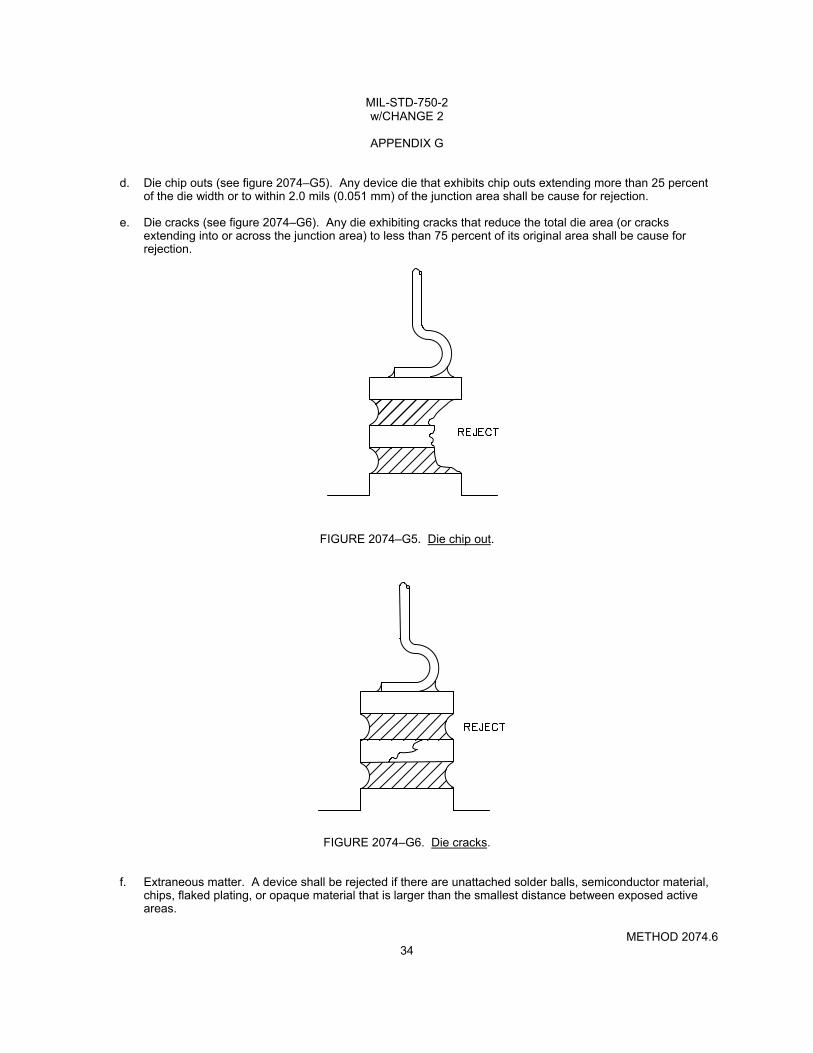
MIL-STD-750-2 w/CHANGE 2
METHOD 2074.6 34
APPENDIX G
d. Die chip outs (see figure 2074–G5). Any device die that exhibits chip outs extending more than 25 percent of the die width or to within 2.0 mils (0.051 mm) of the junction area shall be cause for rejection.
e. Die cracks (see figure 2074–G6). Any die exhibiting cracks that reduce the total die area (or cracks
extending into or across the junction area) to less than 75 percent of its original area shall be cause for rejection.
FIGURE 2074–G5. Die chip out.
FIGURE 2074–G6. Die cracks.
f. Extraneous matter. A device shall be rejected if there are unattached solder balls, semiconductor material, chips, flaked plating, or opaque material that is larger than the smallest distance between exposed active areas.

MIL-STD-750-2 w/CHANGE 2
METHOD 2074.6 35
APPENDIX H
METAL BODY, STUD MOUNTED, SOLDER CONTACT DESIGN
H.1 General. The following inspections shall be made prior to capping. This appendix is a mandatory part of this test method. The information contained herein is intended for compliance.
H.1.1 Die and lead assembly (see figures 2074–H1 and 2074–H2). The die and lead assembly shall be located on the base pedestal so that there is complete contact over the design contact area. The lead shall be free of nicks and scrapes that reduce the lead diameter by more than 5 percent. The die and lead assembly shall not be tilted more than 5 degrees with respect to the base.
FIGURE 2074–H1. Offset die.

MIL-STD-750-2 w/CHANGE 2
METHOD 2074.6 36
APPENDIX H
FIGURE 2074–H2 . Tilted die.
H.1.2 Extraneous matter.
a. Solder slivers and spikes. A device shall be rejected if solder slivers and spikes are not securely attached to the parent body of the solder. A securely attached sliver or spike is one having a cross sectional area greater at the area of attachment than anywhere else on the solder protrusion and having no necked-down areas.
b. Foreign matter. A device shall be rejected if there are unattached solder balls, semiconductor materials,
chips, flaked plating, or opaque material that is larger than the smallest distance between exposed active areas.
c. Multiple die attachments. A device shall be rejected if the attached portion of an adjacent die exceeds 25
percent of the die area.
H.1.3 Assembly defects.
a. Tilted elements. A device shall be rejected if any element of the assembly is tilted in excess of 10 degrees from the normal mounting plane.
b. Misaligned elements. A device shall be rejected if any element of the assembly is misaligned or displaced in
excess of 33 percent of its width from the die or die stack centerline, bridges two active regions, or extends beyond the isolation region of the oxide.

MIL-STD-750-2 w/CHANGE 2
METHOD 2074.6 37
APPENDIX I
METAL BODY, DIAMOND BASE REGULATORS, SOLDER CONTACT DESIGN
I.1 General (see figure 2074–I1). This appendix is a mandatory part of this test method. The information contained herein is intended for compliance.
FIGURE 2074–I1. Diamond base construction.
I.1.1 Die-to-pedestal and die-to-clip solder connections.
a. Solder voids. A device shall be rejected if solder flow is less than 50 percent of the perimeter of the minimum available contact area.
b. Solder overflow. A device shall be rejected if any solder flow bridges from the top to bottom surface of the
die or reduces the normal separation of two active regions by 50 percent or more.
I.1.2 Clip-to-post and feed-through to heat sink solder connections.
a. Solder voids. A device shall be rejected if the wetting action of the solder to each member of the connection is not continuous.
b. Solder overflow. A device shall be rejected if any solder flow extends on to any portion of the weld flange of
the heat sink.

MIL-STD-750-2 w/CHANGE 2
This page is intentionally left blank.
MIL-STD-750-2 w/CHANGE 2
METHOD 2075.1 1 of 1
METHOD 2075.1
DECAP INTERNAL VISUAL DESIGN VERIFICATION
1. Purpose. The purpose of this test method is to verify that design and construction of a semiconductor device are the same as those documented in the qualified design report and for which qualification approval has been granted. This test is destructive and would normally be employed on a sampling basis during qualification, or quality conformance inspection, of a specific device type.
2. Apparatus. Equipment used in this examination shall be capable of demonstrating conformance to the requirements of the applicable acquisition document and shall include optical equipment with sufficient magnification to verify all structural features of the devices.
3. Procedure. Devices shall be selected at random from the inspection lot and examined using sufficient magnification to verify that design and construction are in accordance with the requirements of the applicable design documentation or other specific requirements (see 4). Specimens of constructions which do not contain an internal cavity (e.g., sealed or embedded devices) or those which would experience destruction of internal features of interest as a result of opening, may be obtained from manufacturing prior to sealing. Specimens of constructions with an internal cavity shall be selected from devices which have completed all manufacturing operations and they shall be delidded or opened taking care to minimize damage to the areas to be inspected. When specified by the applicable performance specification sheet, specimens of constructions with an internal cavity may be obtained from manufacturing prior to sealing.
3.1 Photographs of die topography and intraconnection pattern. When specified, a color photograph or transparency shall be made showing the topography of elements formed on the die or substrate and the metallization pattern. This photograph shall be at a minimum magnification of 80X except that if this results in a photograph larger than 3.5 x 4.5 inches (88.90 x 114.30 mm), the magnification may be reduced to accommodate the 3.5 x 4.5 inches (88.90 x 114.30 mm) view. In addition, a color photograph for all qualifications reports and design changes is required. The photograph shall be submitted with the 36D form.
3.2 Failure criteria. Devices which fail to meet the detailed requirements for design and construction shall constitute a failure.
4. Summary. The following conditions shall be specified in the applicable performance specification sheet or acquisition document:
a. Any applicable requirements for design and construction. b. Allowance for obtaining internal cavity devices prior to encapsulation (see 3). c. Requirement for photographic record, if applicable (see 3.1), and disposition of photographs. d. Sample size.

MIL-STD-750-2 w/CHANGE 2
This page is intentionally left blank.

MIL-STD-750-2 w/CHANGE 2
METHOD 2076.4 1 of 14
METHOD 2076.4
RADIOGRAPHY
1. Purpose. The purpose of this test is to nondestructively detect defects within the sealed case of a
semiconductor device, especially those resulting from sealing of the lid to the case, and internal defects such as foreign objects, improper interconnecting wires, and voids in the die attach material. This test method establishes methods, criteria, and standards for radiographic examination of discrete devices.
2. Apparatus. 2.1 Film based radiography. The apparatus and materials for film based radiography shall include:
a. Radiographic equipment with a sufficient voltage range to penetrate the device. The focal distance shall be
adequate to maintain a sharply defined image of an object with a major dimension of .001 inch (0.025 mm). b. Radiographic film (Agfa D2 or equivalent) or medium. The film should be selected to provide the resolution
required to view all internal components, including bond wires. c. Radiographic viewer capable of .001 inch (0.025 mm) resolution in any major dimension. d. Adequate fixtures capable of holding devices in the required positions without interfering with the accuracy
or ease of image interpretation. e. Radiographic quality standards capable of verifying the ability to detect all specified defects for particular
package types being x–rayed. f. A .062 inch (1.57 mm) minimum lead topped table shall be used to prevent back scatter of radiation.
2.2 Real time radiography. The apparatus and materials real time radiography shall include:
a. Radiographic equipment with a sufficient voltage range to penetrate the device. The focal distance shall be
adequate to maintain a sharply defined image of an object with a major dimension of .001 inch (0.025 mm). b. Radiographic viewer/monitor capable of .001 inch (0.025 mm) resolution in any major dimension. c. Holding fixtures capable of holding devices in the required positions (if necessary) without interfering with
the accuracy or ease of image interpretation. d. Radiographic image resolution of real time x–ray equipment shall be such that all specified defects for
particular package types are readily apparent.
3. Procedure.
3.1 Film based radiography. The x–ray exposure factors, voltage, milliampere setting and time settings shall be selected or adjusted as necessary to obtain satisfactory exposures and achieve maximum image details within the sensitivity requirements for the device or defect features the radiographic test is directed toward. Unless otherwise specified, the x–ray voltage shall be the lowest consistent with these requirements and shall not exceed 150 kV. Although higher voltages may be necessary to penetrate certain packages, these levels may be damaging to some device technologies and should only be used when approved by the device manufacturer.
NOTE: For certain case types, the electron shielding effects of device construction materials (packages or internal) may effectively prevent radiographic identification of certain types of defects from some or all possible viewing angles. This factor should be considered in relation to the design of each when application of this test method is specified. If the best attempt to obtain a clear image results in the inability of the Radiographer to clearly see some or all of the rejectable criteria, this must be noted as an exception on the inspection report and certificate of compliance.

MIL-STD-750-2 w/CHANGE 2
METHOD 2076.4 2
3.1.1 Mounting. The devices shall be mounted in the holding fixture so that the devices are not damaged or contaminated and are in the proper plane as specified. The devices may be mounted in any type of fixture and masking with lead diaphragms, or barium clay may be employed to isolate multiple specimens, provided the fixtures or masking materials do not block the path of the x–rays to the film or any portion of the device. The manufacturer shall provide an image of the device, either drawing or photograph, to show the correct construction of the device and the component placement and orientation.
3.1.2 Views.
a. Unless otherwise specified, flat packages and single ended cylindrical devices shall have one view taken with the x–rays penetrating in the Y direction. When more than one view is required, the second and third views, as applicable, shall be taken with the x–rays penetrating in the X and Z directions respectively.
b. Unless otherwise specified, stud-mounted and cylindrical axial lead devices shall have one view taken with
the x–rays penetrating in the X direction. When more than one view is required, the second and third views, as applicable, shall be taken with the x–rays penetrating in the Z direction and at 45 degrees between the X and Z directions.
c. All JANS devices shall have two views minimum. The views should be specified by the manufacturer to
show the all internal components, including bond wires. Extra views shall be specified when necessary to show all bond wires along their length (X1, X2, and Z axis) and the Y axis. Stud-mounted and axial lead device views shall be taken with x–rays penetrating in the X and Z directions.
3.1.3 Radiographic quality standard. The radiographic quality standard shall consist of a suitable standard
penetrameter such as radiographic quality standard ASTM type B - image quality indicator for semiconductor radiography or equivalent device. Each radiograph shall have two image quality standards exposed with each view located (and properly identified) in opposite corners of the film. The radiographic density of penetrameters chosen shall bracket the density of the devices beings inspected. While this is the minimum resolution required, the presence and clarity of these standards does not relieve the requirement to prepare the x–rays to produce images that allow for detailed inspection of the internal components.
3.1.4 Film and marking. When used, the radiograph film shall be in a film holder backed with a minimum of .062 inch (1.57 mm) lead or the holder shall be placed on the lead topped table (see 2.f herein). The film shall be identified using techniques that legibly print the following information, photographically on the radiograph:
a. Device manufacturer's name or code identification number. b. Device type or Part or Identifying Number (PIN). c. Production lot number, date code, or inspection lot number. d. Radiographic film view number and date. e. Device serial or cross reference numbers, when applicable (see 3.3). f. X–ray laboratory identification, if other than device manufacturer. g. X–ray axis views (X, Y, or Z).
3.1.5 Tests. The x–ray exposure factor shall be selected to achieve resolution of .001 inch (0.025 mm) major
dimension, less than 10 percent distortion and an "H" and "D" film density between 1 and 2.5 in the area of interest of the device image. Radiographs shall be made for each view required (see 4 herein.).
3.1.6 Processing. The radiographic film manufacturer's recommended procedure shall be used to develop the exposed film, and the film shall be processed so that it is free of processing defects such as fingerprints, scratches, fogging, chemical spots, and blemishes.

MIL-STD-750-2 w/CHANGE 2
METHOD 2076.4 3
3.2 Real time radiography. The x–ray exposure factors, voltage, milliampere setting, and time settings shall be selected or adjusted as necessary to achieve maximum image details within the sensitivity requirements for the device, or defect features, the radiographic test is directed toward. Unless otherwise specified, the x–ray voltage shall be the lowest consistent with these requirements and shall not exceed 150 kV. Although higher voltages may be necessary to penetrate certain packages, these levels may be damaging to some device technologies. Higher voltages should be used only when approved by the device manufacturer because they are necessary in some cases. Real time radiographic systems shall be characterized for their dose rate. The dose rate should be identified and a safe time limit established to ensure devices under test are not subjected to excessive levels of radiation.
NOTE: The equipment for real time radiography must be capable of producing results of equal quality when compared with film techniques. Digital images shall be screened on a display monitor capable of producing equal or better magnification than that used to screen x–ray film.
3.2.1 Mounting. The devices shall be mounted in the holding fixture or manipulated within the machine so that the
devices are not damaged or contaminated and are in the proper plane as specified. The manufacturer shall provide an image of the device, either drawing or photograph, to show the correct construction of the device and the component placement and orientation.
3.2.2 Views.
a. Unless otherwise specified, flat packages and single ended cylindrical devices shall have three views taken with the x–rays penetrating in the Y direction. When more than one view is required, the second and third views, as applicable, shall be taken with the x–rays penetrating in the X and Z directions respectively. Real time radiography is not limited as with film based radiography, therefore views X, Y, and Z should be taken for each device. The device manufacturers recommended directions should be included as well.
b. Unless otherwise specified, stud–mounted and cylindrical axial lead devices shall have one view taken with
the x–rays penetrating in the X direction. When more than one view is required, the second and third views, as applicable, shall be taken with the x–rays penetrating in the Z direction and at 45 degrees between the X and Z directions.
c. All JANS devices shall have two views minimum. The views should be specified by the device manufacturer
to show all internal components, including bond wires. Extra views shall be specified when necessary to show all bond wires along their length (X1, X2, and Z axis.) and the Y axis. Stud–mounted and axial lead device views shall be taken with x–rays penetrating in the X and Z directions.
3.2.3 Records. Records are required and shall be retained for the period specified. The use of formats such as
CD-ROM's and DVD recordings of radiography procedure are allowed with the permission of the qualifying activity, provided the proper clarity, definition, and magnification can be demonstrated. Data storage should include the following information in a data summary sheet stored with the images as a means of identification.
a. Device manufacturer's name or code identification number. b. Device type or Part or Identifying Number (PIN). c. Production lot number, date code, or inspection lot number. d. The machine number and date. e. Device serial or cross reference numbers, when applicable (see 3.3 herein). f. X–ray laboratory identification, if other than device manufacturer.

MIL-STD-750-2 w/CHANGE 2
METHOD 2076.4 4
3.3 Serialized devices. When device serialization is required, each device shall be readily identified by a serial number. The devices shall be radiographed and identified by serial number in consecutive, increasing serial order. When a device is missing, the blank space shall contain either the serial number or other x–ray opaque objects to readily identify and correlate the x–ray data. When more than one consecutive device is missing within serialized devices, the serial number of the last device before the skip and the first device after the skip may, at the manufacturer’s option, be used in place of the multiple opaque objects.
3.4 Special device marking. When specified (see 4.c herein), the devices that have been x–rayed and found acceptable shall be identified with a blue dot on the external case. The blue dot shall be approximately .062 inch (1.57 mm) in diameter. The color selected from FED–STD–595 shall be any shade between 15102–15123 (gloss blue) or 25102–25109 (semi-gloss blue). The dot shall be placed so that it is readily visible but shall not obliterate other device markings. (Other colors, for example green, can also be used.) Use blue dot for film radiography and green dot for real time radiography.
3.5 Operating personnel. Personnel who will perform radiographic inspection shall have training in radiographic procedures and techniques so that defects revealed by this method can be validly interpreted and compared with applicable standards. Operators shall be trained and certified in the operation of the specific real time radiographic system they operate. The following minimum vision requirements shall apply for visual acuity of personnel inspecting film as well as personnel authorized to conduct radiographic tests:
a. Distant vision shall equal at least 20/30 in both eyes, corrected or uncorrected. b. Near vision shall be such that the operator can read Jaegger type No. 2 at a distance of 16 inches (406.4
mm), corrected or uncorrected. c. Vision tests shall be performed by an oculist, optometrist, or other professionally recognized personnel at
least once a year.
3.6 Interpretation of radiographs. Utilizing the equipment specified herein, radiographs shall be inspected to determine if each device conforms to this standard or if it is defective and shall be rejected. Interpretation of the radiograph shall be made under low light level conditions without glare on the radiographic viewing surface. The radiographs shall be examined on a suitable illuminator with variable intensity or on a viewer suitable for radiographic inspection on projection type viewing equipment. The radiograph shall be viewed at a magnification of between 10X and 40X (minimum), which shows the entire area of interest at once (entire die bond, entire device lid, etc.) in the field of view. If a problem is suspected during the initial review, then the device shall be re-viewed using a magnification of up to 100X. Viewing masks may be used when necessary. Any radiograph not clearly illustrating the features in the radiographic quality standards is not acceptable and another radiograph of the devices shall be taken. In the event that parts of the device cannot be clearly seen and evaluated in accordance with 3.8 herein, the Radiographer shall so note on the radiography report that the criteria has not been evaluated and cannot be confirmed.
3.6.1 Interpretation of real time images. Utilizing the equipment specified herein, real time images shall be inspected to determine if each device conforms to this standard or if it is defective and shall be rejected. The radiograph shall be viewed on the screen such that the image fills the entire field of view with the area of interest at once (entire die bond, entire device lid, etc.) at a magnification comparable to 10X – 40X (minimum). See 3.6 herein for appropriate viewing magnifications. The image shall not be enlarged to the extent that resolution of the image does not clearly illustrate the features in the radiographic quality standard. The radiographs shall be examined on a monitor that provides resolution for viewing compatible with the requirements as noted in 3.2 herein. Viewing masks may be used when necessary. Any radiograph not clearly illustrating the features in the radiographic quality standards is not acceptable and another radiograph of the devices shall be taken. In the event that parts of the device cannot be clearly seen and evaluated in accordance with 3.7 herein, the Radiographer shall so note on the radiography report that the criteria has not been evaluated and cannot be confirmed.

MIL-STD-750-2 w/CHANGE 2
METHOD 2076.4 5
3.7 Reports and records.
3.7.1 Reports of inspection. For JANS devices, or when specified for other device classes, the manufacturer shall furnish inspection reports with each shipment of devices. The report shall describe the results of the radiographic inspection, and list the order number or equivalent identification, the PIN, the date code, the quantity inspected, the quantity rejected, and the date of test. For each rejected device, the PIN, the serial number, when applicable, and the cause for rejection shall be listed. Any criteria that cannot be evaluated due to resolution of the film (or real time equipment) shall be noted on the report.
3.7.2 Radiograph submission. When specified, one set of the applicable radiographs shall accompany each shipment of devices. Real time radiography image results submitted on suitable media will be provided.
3.7.3 Radiograph and report retention. When specified, the device manufacturer shall retain a set of the radiographs or a set of the real time radiography images and a copy of the inspection report for the period specified.
3.8 Examination and acceptance criteria.
3.8.1 Device construction. Acceptable devices shall be of the specified design and construction with regard to the characteristics discernible through radiographic examination. Devices that deviate significantly from the specified construction shall be rejected.
3.8.2 Individual device defects. The individual device examination shall include, but not be limited to, inspection for foreign particles, solder or weld "splash" build up of bonding material, proper shape and placement of lead wires or whiskers, and bond of lead or whisker to semiconductor element. Devices for which the radiograph reveals any of the following defects shall not be accepted.
3.8.2.1 Presence of extraneous material. Extraneous matter or foreign particles shall include:
a. Any foreign material greater than .003 inch (0.076 mm) or of any lesser size which is sufficient to bridge non-connected conducting elements of the device.
b. Any wire tail extending beyond its bond end by more than two diameters at the semiconductor bond pad or
by more than four wire diameters at the package post. c. Any burr on a post greater than .003 inch (0.076 mm) in its major dimension. d. Metal flaking on the header or posts inside the package. e. Excessive bonding material build-up.
(1) Bonding material that is higher than one times the height of the semiconductor die. (2) There shall be no visible loose extraneous material greater than .001 inch (0.025 mm) allowed.
Excessive bonding material which is not loose and passes the requirements of 3.8.2.1.e.(1) shall be allowed unless the height of the accumulation is greater than the width of its base or the material necks down at any point from the top of the accumulation to the base.

MIL-STD-750-2 w/CHANGE 2
METHOD 2076.4 6
3.8.2.2 Thermal integrity. For thermal integrity, total contact area voids in excess of 15 percent of the total contact area, for all power and case mounted devices and 30 percent for all other devices is rejectable, unless otherwise specified on the applicable specification sheet. If 5 percent or more of the devices in a JANS inspection lot fail this die attach criteria, the lot shall be reviewed and appropriate corrective action shall be taken. In addition, if the die attach image shows any unusual anomalies or any significant voiding directly under the active area or multiple relatively large voids, the lot shall be reviewed and appropriate corrective action shall be taken.
3.8.2.3 Unacceptable construction. In the examination of devices, the following conditions shall be considered unacceptable construction and devices that exhibit any of the following defects shall be rejected:
a. Wires present, other than those connecting specific areas of the semiconductor die to the external leads. b. Angle between semiconductor die surface and edge less than 45 degrees.
3.8.2.3.1 Voids (see figure 2076–1). A single void which traverses either the length or width of the semiconductor
die and exceeds 10 percent of the total intended contact area. When radiographing devices, certain types of mounting do not give true representations of voids. When such devices are inspected, the mounting shall be noted on the inspection report.
3.8.2.3.2 Defective seal (see figure 2076–2). Any device wherein the lid seal (including the seal fillet) is not continuous or is reduced from its designed sealing width by more than 75 percent. The intended seal width may be reduced by multiple voids (not to include pin hle voids).
NOTE: Expulsion resulting from the final sealing operation is not considered extraneous material as long as it
can be established that it is continuous, uniform, and attached to the parent material and does not exhibit a ball, splash, or tear-drop configuration.
3.8.2.3.3 Inadequate clearance. Acceptable devices shall have adequate internal clearance to assure that the
elements cannot contact one another or the case. No crossover of wires connected to different electrical elements shall be allowed. Depending upon the case type, devices shall be rejected for the following conditions:
a. Flat pack and dual-in-line (see figure 2076–3).
(1) Any lead wire that appears to touch or cross another lead wire or bond (Y plane only). (2) Any lead wire that deviates from a straight line from bond to external lead and appears to be within
.002 inch (0.0504 mm) of another bond (Y plane only). (3) Lead wires that do not deviate from a straight line from bond to external lead and appear to touch
another wire or bond (Y plane only). (4) Any lead wire that touches or is less than .002 inch (0.0504 mm) from the case or external lead to
which it is not attached (X and Y plane). (5) Any bond that is less than .001 inch (0.0254 mm) (excluding bonds connected by a common
conductor) from another bond (Y plane only). (6) Any wire making a straight line run (with no arc) from die bonding pad to package post. (7) Any cracks, nicks, neckdown, or cuts on lead wires that reduces the wire diameter by more than 25
percent

MIL-STD-750-2 w/CHANGE 2
METHOD 2076.4 7
(b) Round or "box" transistor type (see figure 2076–4).
(1) Any lead wire that touches or is less than .002 inch (0.0504 mm) from the case or external lead to which it is not attached (X and Y plane).
(2) Lead wires that sag below an imaginary plane across the top of the bond (X plane only).
(3) Any lead wire that appears to touch or cross another lead wire or bond (Y plane only) if bonded to different electrical elements.
(4) Any lead wire that deviates from a straight line from bond to external lead appears to touch or to be within .002 inch (0.0504 mm) of another wire or bond (Y plane only).
(5) Any bond that is less than .001 inch (0.0254 mm) (excluding bonds connected by a common conductor) from another bond (Y plane only).
(6) Any wire making a straight line run (with no arc) from die bonding pad to package post, unless specifically designed in this manner (e.g., clips, rigid connecting leads, or heavy power leads).
(7) Any internal post that is bent more than 10 degrees from the vertical (or intended design position), or is not uniform in length and construction, or comes closer than one post diameter to another post.
(8) Any post in a low profile case (such as a TO–46) which comes closer to the top of the case than 20 percent of the total inside dimension between the header and the top of the case. Any device in which the semiconductor element is vertical to the header, and comes closer than .002 inch (0.0504 mm) to the header, or to any part of the case.
(9) Any cracks, nicks, neckdown, or cuts on lead wires that reduces the wire diameter by more than 25 percent.
c. Axial lead type (see figure 2076–5).
(1) Whisker embedded within glass body wall.
(2) Whisker tilted more than 5 degrees in any direction from the device lead axis or deformed to the extent that it touches itself.
(3) Either half of an S or C bend whisker that is compressed so that any dimension is reduced to less than 50 percent of its design value. On diodes with whiskers metallurgically bonded to the post and to the die, the whisker may be deformed to the extent that it touches itself if the minimum whisker clearance zone specified on figure 2076–6 is maintained for metal packages.
(4) Whiskerless construction device with plug displacement distance more than one-fourth of the diameter of the plug with respect to the central axis of the device.
(5) Semiconductor element mounting tilted more than 15 degrees from normal to the main axis of the device.
(6) Die hanging over edge of header or pedestal more than 20 percent of the die contact area by design.
(7) Less than 75 percent of the semiconductor element base area is bonded to the mounting surface.
(8) Voids in the welds which reduce the lead to plug connection by more than 25 percent of the total weld area.
(9) Devices with package deformities such as body glass cracks, incomplete seals (e.g., voids, position of glass), die chip outs, and severe misalignment of S and C shaped whisker connections to die or post that exceed the limits of the applicable visual inspection requirements.
MIL-STD-750-2 w/CHANGE 2
METHOD 2076.4 8
3.8.3 Encapsulated non-cavity assemblies of discrete devices. External to the individual devices, the encapsulating material shall be examined and rejected for the following defects:
a. Extraneous material of any shape with any dimension exceeding .020 inch (0.51 mm). b. Any two adjacent particles of such matter with total dimensions exceeding .030 inch (0.76 mm).
4. Summary. The following conditions shall be specified in the applicable performance specification sheet or
acquisition document:
a. Number of views, if other than indicated in 3.1.2 and 3.2.2. b. Radiograph submission, if applicable (see 3.7.2). c. Marking, if other than indicated in 3.3 and marking of samples to indicate they have been radiographed, if
required (see 3.4). d. Sample defects and criteria for acceptance or rejection, if other than indicated in 3.8. e. Radiograph and report retention, if applicable (see 3.7.3). f. Test reports when required.

MIL-STD-750-2 w/CHANGE 2
METHOD 2076.4 9
FIGURE 2076–1. Acceptable and unacceptable voids and excessive pigtails.

MIL-STD-750-2 w/CHANGE 2
METHOD 2076.4 10
NOTE: This figure is not intended to represent the required viewing magnification. It is only
intended to illustrate how lid seal voiding is calculated.
FIGURE 2076–2. Lid seal voids and rejection criterion (drawing).

MIL-STD-750-2 w/CHANGE 2
METHOD 2076.4 11
FIGURE 2076–3. Clearance in dual-in-line or flat pack type device.
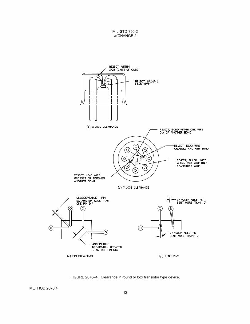
MIL-STD-750-2 w/CHANGE 2
METHOD 2076.4 12
FIGURE 2076–4. Clearance in round or box transistor type device.
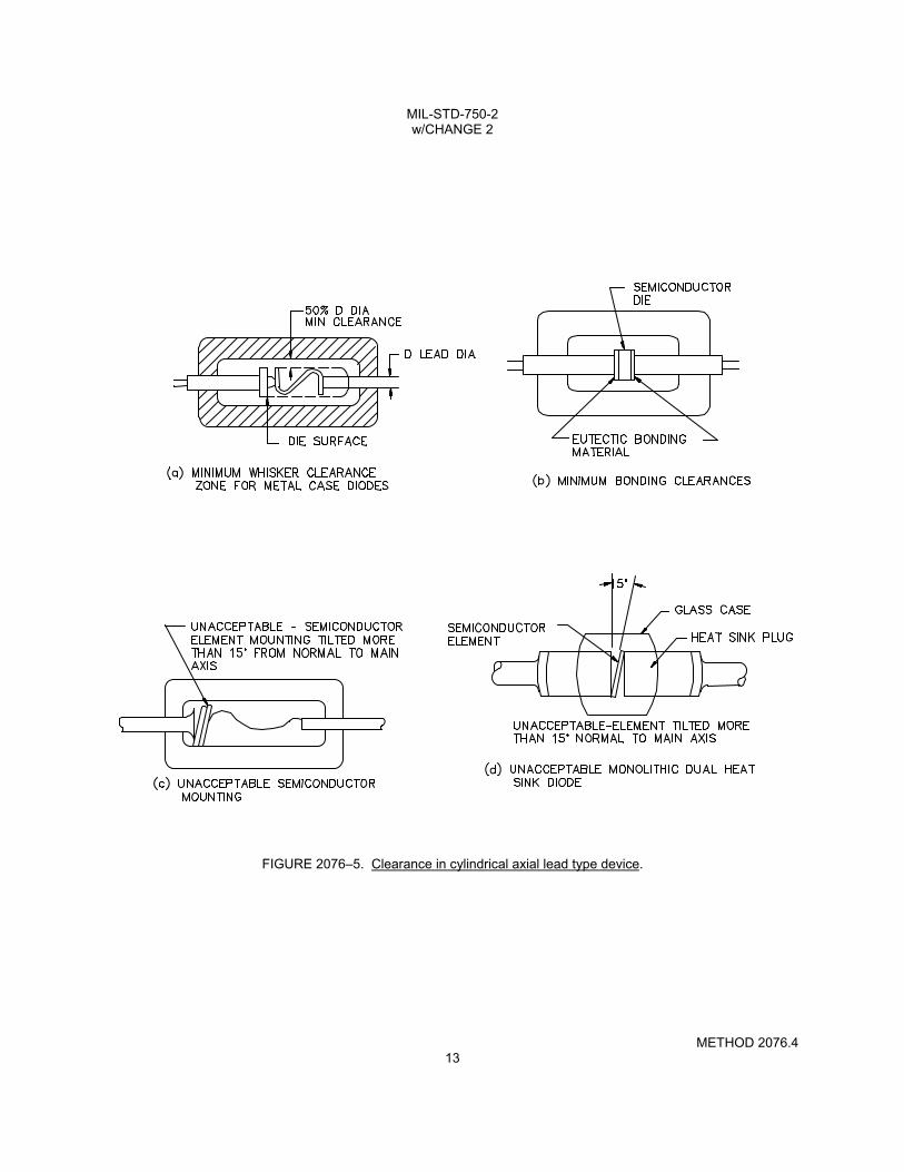
MIL-STD-750-2 w/CHANGE 2
METHOD 2076.4 13
FIGURE 2076–5. Clearance in cylindrical axial lead type device.

MIL-STD-750-2 w/CHANGE 2
METHOD 2076.4 14
FIGURE 2076–6. Typical digital radiography view of a UB device.
MIL-STD-750-2 w/CHANGE 2
METHOD 2077.4 1 of 24
METHOD 2077.4
SCANNING ELECTRON MICROSCOPE (SEM) INSPECTION OF METALLIZATION
1. Purpose. This test method provides a means of judging the quality and acceptability of metallization on semiconductor dice. It addresses the specific metallization defects that are batch process oriented and which can best be identified utilizing this test method. It should not be used as a test method for workmanship and other type defects best identified using the visual inspection criteria of test method 2072 of this standard. The term, "dice", for the purpose of this test method, includes diodes and transistors which have expanded metallization contacts or metallization interconnects.
1.1 Definitions.
1.1.1 Barrier adhesion metal. The lower layer of multi-layer metal system deposited to provide a sound mechanical bond to silicon/silicon oxide surfaces or to provide a diffusion barrier of a metal into an undesired area such as aluminum into a contact window.
1.1.2 Cross-sectional plane. An imaginary plane drawn perpendicular to current flow and which spans the entire width of the metallization stripe as illustrated on figure 2077–1. Metallization stripes over topographical variations (e.g., passivation steps, cross-overs, bird's head), which are nonperpendicular to current flow, are projected onto cross-sectional planes for purposes of calculating cross-sectional area reductions.
1.1.3 Destructive SEM. The use of specific equipment parameters and techniques that result in unacceptable levels of radiation damage or contamination of the inspected semiconductor structure.
1.1.4 Directional edge. A directional edge (see figure 2077–2) is typically the edge(s) of a rectangular contact window over which metallization may be deposited for the purpose of carrying current into, through, or out of the contact window for device operation. It should be noted that contact geometry, site of concern, or both may vary and if so, the directional edge concept should be modified accordingly.
1.1.5 General metallization (conductors). The metallization at all locations including metallization (stripes) in the actual contact window regions with the exception being at areas of topographical variation (e.g., passivation steps, bird's head, cross-overs).
1.1.6 Glassivation. Glassivation is the top layer(s) of transparent insulating material that covers the active circuit area (including metallization), except bonding pads and beam leads.
1.1.7 Interconnection. The metal deposited into a via to provide an electrical conduction path between isolated metal layers.
1.1.8 Major current-carrying directional edge (see figure 2077–2). The directional edge(s) which is designed to provide a path for the flow of current into, through, or out of a contact window or other area(s) of concern.
1.1.9 Multi-layer metallization (conductors). Two or more layers of metal used for electrical conduction that are not isolated from each other by a grown or deposited insulating material. The term "underlying metal" shall refer to any layer below the top layer of metal.
1.1.10 Multi-level metallization (conductors). A single layer or a multi-layer of metal shall represent a single level of metallization. A combination of such levels, isolated from each other by a grown or deposited layer of insulating material, shall comprise the multi-level metallization interconnection system. The use of vias to selectively connect portions of such level combinations through the isolation shall not effect this definition.

MIL-STD-750-2 w/CHANGE 2
METHOD 2077.4 2
1.1.11 Nondestructive SEM. The use of specific equipment parameters and techniques that result in negligible radiation damage, contamination, or both of the inspected semiconductor structure.
1.1.12 Passivation. The silicon oxide, nitride or other insulating material that is grown or deposited on the die prior to metallization.
1.1.13 Passivation steps. The vertical or sloped surface resulting from topographical variations of the wafer surface (e.g., contact windows, diffusion cuts, vias, etc.).
1.1.14 Via. The opening in the insulating layer to provide a means for deposition of metal to interconnect layers of metal.
1.1.15 Wafer lot. A wafer lot consists of semiconductor wafers formed into a lot at the start of wafer fabrication for homogeneous processing as a group and assigned a unique identifier or code to provide traceability and maintain lot integrity throughout the fabrication process.
2. Apparatus. The apparatus for this inspection shall be a scanning electron microscope (SEM) having an ultimate resolution of 100 Å or less and a variable magnification to at least 20,000X. The apparatus shall be such that the specimen can be tilted to a viewing angle (see figure 2077–3) of 60 degrees or greater, and can be rotated through 360 degrees. Evidence of using competent SEM operating personnel, as well as acceptable techniques and equipment that meet the requirements of this test method, shall be demonstrated for the approval of the qualifying activity or, when applicable, a designated representative of the acquiring activity.
3. Procedure.
3.1 Sample selection. Proper sampling is an integral part of this test method. Statistical techniques, using random selection, are not practical here because of the large sample size that would be required. This test method specifies means of minimizing test samples while maintaining confidence in test integrity by designating for examination wafers in specific locations on the wafer holder(s) in the metallization chamber, and specific dice on the wafers. These dice are in typical or worst case positions for the metallization configuration. Dice selected for SEM examination shall not be immediately adjacent to the wafer edge, and they shall be free of smearing or inking, since this could obscure processing faults for which they are to be inspected. Metallization acceptance shall be based on examination of sample dice, using either a single wafer acceptance basis or a process lot acceptance basis. A process lot is a batch of wafers which has been received together, those common processes which determine the slope and thickness of the oxide step and which have been metallized as a group.
NOTE: When die or packaged parts are to be evaluated for wafer lot acceptance and the requirements for wafer selection in accordance with table 2077–I cannot be met, the following sample size shall be utilized:
a. If the die or packaged part is from a known homogeneous wafer lot (traceability specific to the wafer or wafer
lot and objective evidence is available for verification), then the sample size shall be 8 devices randomly selected from the population.
b. If the die or packaged part is from a non-homogeneous wafer lot (traceability is unknown or no objective
evidence is available for verification), then the sample size shall be 22 devices randomly selected from the population.
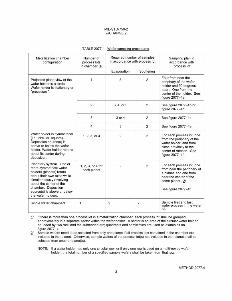
MIL-STD-750-2 w/CHANGE 2
METHOD 2077.4 3
TABLE 2077–I. Wafer sampling procedures.
Metallization chamber
configuration
Number of
process lots in chamber 1/
Required number of samples in accordance with process lot
Sampling plan in accordance with
process lot Evaporation Sputtering
Projected plane view of the wafer holder is a circle. Wafer holder is stationary or "precesses".
1 5 2
Four from near the periphery of the wafer holder and 90 degrees apart. One from the center of the holder. See figure 2077–4a.
2 3, 4, or 5 2 See figure 2077–4b or
figure 2077–4c.
3 3 or 4 2 See figure 2077–4d.
4 3 2 See figure 2077–4e.
Wafer holder is symmetrical (i.e., circular, square). Deposition source(s) is above or below the wafer holder. Wafer holder rotates about its center during deposition.
1, 2, 3, or 4 2 2 For each process lot, one
from the periphery of the wafer holder, and from close proximity to the center of rotation. See figure 2077–4f.
Planetary system. One or more symmetrical wafer holders (planets) rotate about their own axes while simultaneously revolving about the center of the chamber. Deposition source(s) is above or below the wafer holders.
1, 2, 3, or 4 for
each planet 2 2 For each process lot, one
from near the periphery of a planet, and one from near the center of the same planet. 2/ See figure 2077–4f.
Single wafer chambers
1 2 2 Sample first and last
wafer process in the wafer lot.
1/ If there is more than one process lot in a metallization chamber, each process lot shall be grouped approximately in a separate sector within the wafer holder. A sector is an area of the circular wafer holder bounded by two radii and the subtended arc; quadrants and semicircles are used as examples on figure 2077–4.
2/ Sample wafers need to be selected from only one planet if all process lots contained in the chamber are included in that planet. Otherwise, sample wafers of the process lot(s) not included in that planet shall be selected from another planet(s).
NOTE: If a wafer holder has only one circular row, or if only one row is used on a multi-rowed wafer
holder, the total number of a specified sample wafers shall be taken from that row.

MIL-STD-750-2 w/CHANGE 2
METHOD 2077.4 4
3.1.1 Sampling condition A, unglassivated devices. This sampling condition applies to devices which have no glassivation over the metallization. Steps 1 and 2 (see 3.1.1.1 and 3.1.1.2 herein), both apply when acceptance is on a lot acceptance basis. Only step 2 applies when acceptance is on a single wafer acceptance basis.
3.1.1.1 Step 1: Slice selection. From each lot to be examined on a lot acceptance basis, wafers shall be selected from the designated positions on the wafer holder(s) in the metallizing chamber. For single wafer systems, the first and last wafers processed from each wafer lot shall be selected. In accordance with the definition of lot in 3.1, if there is more than one process lot in a metallization chamber, each process lot shall be grouped approximately in a separate sector within the wafer holder, and a separate set of wafers shall be selected for each process lot being examined on a lot acceptance basis. Table 2077–I and figure 2077–4 specify the number and sites of wafers to be selected. Dice selection from the selected wafers shall be in accordance with the sampling plan established for a single wafer in step 2 (see 3.1.1.2).
3.1.1.2 Step 2: Dice selection. When a wafer is to be evaluated (for acceptance on a single wafer basis, or with one or more wafers on a lot acceptance basis), either of the following sampling conditions may be used at the manufacturer's option.
3.1.1.2.1 Sampling condition A1: Quadrants. Immediately following the dicing operation (i.e., scribe and break, saw, etch) and before relative die location on the wafer is lost, four dice shall be selected. The positions of these dice shall be near the periphery of the wafer and approximately 90 degrees apart (see figure 2077–4).
3.1.1.2.2 Sampling condition A2: Segment. After completion of all processing steps and, prior to dicing, two segments shall be separated from opposite sides of each wafer to be examined. These segments shall be detached along a chord approximately one-third of the wafer radius in from the edge of the wafer. One die from near each end of each segment (i.e., four dice) shall then be subjected to SEM examination.
3.1.2 Sampling condition C: Glassivated devices. This sampling condition applies to devices which have glassivation over the metallization. Steps 1 and 2 (see 3.1.2.1 and 3.1.2.2 herein), both apply when acceptance is on a lot acceptance basis. Only step 2 applies when acceptance is on a single wafer acceptance basis.
3.1.2.1 Step 1: Wafer selection. From each lot to be examined on a lot acceptance basis, wafers shall be selected from the designated positions on the wafer holder in the metallizing chamber. For single wafer systems the first and last wafers processed from each wafer lot shall be selected. In accordance with the definition of lot in 3.1, if there is more than one process lot in a metallization chamber, each process lot shall be grouped approximately in a separate sector within the wafer holder, and a separate set of wafers shall be selected for each process lot being examined on a lot acceptance basis. Table 2077–I and figure 2077–4 specify the number and sites of wafers to be selected. Dice selection from the selected wafers shall be in accordance with the sampling plan established for a single wafer in step 2 (see 3.1.2.2).
3.1.2.2. Step 2: Dice selection. When a wafer is to be evaluated (for acceptance on a single wafer acceptance basis, or with one or more other wafers on a lot acceptance basis), any of the following sampling conditions may be used at the manufacturer's option.
3.1.2.2.1 Sampling condition B1: Quadrants. This is the recommended condition for glassivated devices. Immediately following the dicing operation (i.e., scribe and break, saw, etch) and before relative die location on the wafer is lost, four dice shall be selected. The positions of these dice shall be near the periphery of the wafer and approximately 90 degrees apart. The glassivation shall then be removed from the dice using a suitable etch. It is recommended that the etchant used have an etch rate for the glassivation which is approximately 200 times that for the metallization. The dice shall be periodically examined during glass removal using a bright field metallurgical microscope to determine when all the glassivation has been removed and to minimize the possibility of etching the metallization.

MIL-STD-750-2 w/CHANGE 2
METHOD 2077.4 5
3.1.2.2.2 Sampling condition B2: Segment, prior to glassivation. This sampling condition may be used only if the glassivation processing temperature is lower than +400°C. Two segments shall be separated from opposite sides of each wafer to be examined immediately before the glassivation coating operation; (i.e., subsequent to metallization, etching, and sintering, but before glassivation). These segments shall be detached along a chord approximately one-third of the wafer radius in from the edge of the wafer. One die from near each end of each segment (i.e., four dice) shall be subjected to SEM examination.
3.1.2.2.3 Sampling condition B3: Segment, after glassivation. Two segments shall be separated from opposite sides of each wafer subsequent to sintering and glassivation. These segments shall be detached along a chord approximately one-third of the wafer radius in from the edge of the wafer. The glassivation shall then be removed from the segment using a suitable etch (see 3.1.2.2.1 herein for the etch rate). The segment shall be periodically examined using a bright field metallurgical microscope to determine when all the glassivation has been removed and to minimize the possibility of etching the metallization. One die from near each end of each segment (i.e., four dice) shall be subjected to SEM examination.
3.2 Lot control during SEM examination. After dice sample selection for SEM examination, the manufacturer may elect either of two options as follows.
3.2.1 Option 1. The manufacturer may continue normal processing of the lot with the risk of later recall and rejection of product if SEM inspection, when performed, shows defective metallization. If this option is elected, positive control and recall of processed material shall be demonstrated by the manufacturer by having adequate traceability documentation.
3.2.2 Option 2. Prior to any further processing, the manufacturer may store the dice or wafers in a suitable environment until SEM examination has been completed and approval for further processing has been granted.
3.3 Specimen preparation. Specimens shall be mounted in an appropriate manner for examination. Suitable caution shall be exercised in the use of materials such as conducting paints and adhesives for specimen mounting so that important features are not obscured. Non-cross sectioned specimens shall not be coated with any conductive material, as this drastically reduces the contrasts viewable on the SEM. However, cross-sectioned specimens shall be coated with a thin vapor deposited or sputtered film conductive coating if a conventional high vacuum SEM is used for examination. This is required in order to attain the contrast resolution necessary to view these specimens. Controls shall be established to ensure that no artifacts are introduced in the coating. If a variable pressure environmental SEM (ESEM) is used to examine specimens under low vacuum, it may not be necessary to coat cross sectioned samples if image resolution is adequate.
3.4 Specimen examination, general requirements. The metallization on all four edge directions shall be examined on each die for each type of contact window step and for each other types of oxide steps (see table 2077–II). (Oxide refers to any insulating material used on the semiconductor die, whether SiOx or SiNx). A single window (or other type of oxide step) may be viewed if metallization covers the entire window (or other type of oxide step) extending up to and over each edge, and onto the top of the oxide at each edge. Other windows (or other types of oxide steps) on the die shall be examined to meet the requirement that all four directional edges of each type of window (or other type of oxide step) shall be examined on each die. General metallization defects, such as peeling and voids, shall be viewed to provide for the best examination for those defects. When an aerial view does not provide adequate detail for determining step coverage, the specimen shall be cross sectioned.

MIL-STD-750-2 w/CHANGE 2
METHOD 2077.4 6
TABLE 2077–II. Examination procedure for sample dice.
Device type
Area of
examination Examination Minimum - maximum
magnification
Photographic
documentation 1/
Expanded contact bipolar and power FET's (see 3.5.1)
Oxide step (contact windows and other types of oxide steps) 2/
All 4,000X to
20,000X
Two of the worst case oxide steps.
General metallization 3/
All 1,000X
to 6,000X
Worst case general metallization.
1/ See 3.8 (an additional photograph may be required). 2/ Scanning examination shall include all four directional edges of oxide steps (documentation need only show
the worst case). Oxide steps include contact windows (emitters, bases, collectors, drains, sources, diffused resistors) and other types (i.e., diffusion cuts for emitters, bases, collectors, and field oxide steps). See 3.7.1 herein for accept/reject criteria.
3/ See 3.8 herein for accept/reject criteria.
NOTE: For multi-layered-metal interconnection systems, see 3.5.3 and 3.7.3 herein. Window coverage also shall be examined.
3.4.1 Viewing angle (see figure 2077–3). Specimens shall be viewed at an appropriate angle to accurately assess the quality of the metallization. Contact windows are normally viewed at an angle of 45 degrees to 60 degrees or greater.
3.4.2. Viewing direction. Specimens shall be viewed in an appropriate direction to accurately assess the quality of the metallization. This inspection shall include examination of metallization at the edges of contact windows and other types of oxide steps (see 3.4 herein) in any direction that provides clear views of each edge and that best displays any defects at the oxide step. The viewing direction may be perpendicular to an edge, parallel with an edge, or at some oblique angle.
3.4.3 Magnification. The magnification ranges shall be between 4,000X and 20,000X for examination of oxide steps and between 1,000X and 6,000X for general metallization defects, such as peeling and voids (refer to table 2077–II). When dice are subjected to reinspection, such reinspection shall be accomplished at any magnification within the specified magnification.
3.5 Specimen examination detail requirements.
3.5.1 Expanded contact bipolar. Examination shall be as specified herein and summarized in table 2077–II.
3.5.1.1 Oxide steps. Inspect the metallization at all types of oxide steps (see table 2077–II) and document in accordance with 3.8 herein.
3.5.1.2 General metallization. Inspect all general metallization on each die for defects such as peeling and voids. Document in accordance with 3.8 herein.

MIL-STD-750-2 w/CHANGE 2
METHOD 2077.4 7
3.5.2 Power FETs. Examination shall be specified herein and summarized in table 2077–II.
3.5.2.1 Oxide steps. Inspect the metallization at all types of oxide steps (see table 2077–II) and document in accordance with 3.8 herein. For RF or power transistors with interdigitated or mesh structures, each base-emitter stripe pair within each pattern shall be inspected as a minimum. Particular attention shall be directed to lateral etching defects and undercut at base and emitter oxide steps. Documentation shall be as specified in 3.8.
3.5.2.2 General metallization. Inspect all general metallization on each die for defects such as peeling and voids. Document in accordance with 3.8 herein.
3.5.3 Multi-layered metal interconnection systems. Multi-layered metal is defined as two or more layers of metal or any other material used for interconnections. Each layer of metal shall be examined. The principal current-carrying layer shall be examined with the SEM; the other layers (i.e., barrier or adhesion) may be examined using either the SEM or an optical microscope, at the manufacturer's option. Accept/reject criteria for multi-layered metal systems are given in 3.7.3 herein. The glassivation (if any) and each successive layer of metal shall be stripped by selective etching with suitable reagents, layer-by-layer, to permit the examination of each layer. If it is impractical to remove the metal on a single die layer-by-layer, one or more dice immediately adjacent to the original die shall be etched so that all layers shall be exposed and examined. Specimen examination shall be in accordance with 3.5 herein.
3.5.4 Circular or multisided contacts and vias. In devices with circular or multisided contacts and vias, the specimen shall be cross-sectioned to accurately determine the actual cross sectional area.
3.6 Acceptance requirements.
3.6.1. Single slice acceptance basis. The metallization of a wafer shall be judged acceptable only if all sample dice from that wafer are acceptable.
3.6.2 Lot acceptable basis. An entire lot shall be judged acceptable only when all sample dice from all sample wafers are acceptable. At the manufacturer's option, if a lot is rejected in accordance with this paragraph, each wafer from that lot may be individually examined. Acceptance shall then be in accordance with 3.6.1 herein.
3.7 Accept/reject criteria. Rejection of dice shall be based upon batch process oriented defects. Rejection shall not be based upon workmanship and other type defects such as scratches, smeared metallization, or tooling marks. In the event that the presence of such defects obscures the detailed features being examined, an additional die shall be examined which is immediately adjacent to the die with the obscured metallization. Illustrations of typical defects are shown on figure 2077–5 through figure 2077–22.
3.7.1 Oxide steps. The metallization on all four directional edges of every type of oxide step(s) (contact window or other type of oxide step) shall be examined (see 3.4.2 herein). The metallization shall be unacceptable if thinning and one or more defects such as voids, separations, notches, cracks, depressions, or tunnels reduce the cross-sectional area of the metal at the directional edge to less than 50 percent of metal cross-sectional area on either side of the directional edge. When less than 50 percent, for the metallization to be acceptable, all four directional edges shall be covered with metallization (see 3.4.2 herein) and shall be acceptable except in the cases described in 3.7.1.1 and 3.7.1.2 herein.
3.7.1.1 Oxide steps without metallization. In the event that a directional edge profile of a particular type of oxide step cannot be found which is covered with metallization (see 3.4.2 herein) and therefore, a judgment of the quality of the metallization at that directional edge profile cannot be made, this shall not be cause for rejection if:
a. It is established that the edge profile from which metal is absent does not occur in a current-carrying direction, such determination being made either by scanning all oxide steps of this type on the balance of the die, or by examination of a topographical map supplied by the manufacturer which shows the metal interconnect pattern, and;
b. Duplicate sample wafers are examined, these duplicates being located adjacent to the original sample
wafers, in the wafer holder, and being rotated so as to be oriented approximately 180 degrees with respect to the original sample wafers during metallization.
c. If the conditions of both 3.7.1.1.a. and 3.7.1.1.b. are met, a lot acceptance basis may be used. If only
condition a is met, a single wafer acceptance basis must be used.

MIL-STD-750-2 w/CHANGE 2
METHOD 2077.4 8
3.7.1.2 Oxide steps with less than 50 percent metallization. Any combination of defects and thinning over a step which reduces the cross-sectional area of the metal to less than 50 percent of metal cross-sectional area as deposited on the flat surface, shall be cause for rejection. If less than the specified percent of the metallization is present at a particular directional edge profile (see figure 2077–5), wafer lot rejection shall not be invoked if:
a. It is established that the edge profile from which metal is absent does not occur in a current-carrying direction, such determination being made either by scanning all oxide steps of this type on the balance of the die, or by examination of a topographical map supplied by the manufacturer which shows the metal interconnect pattern;
b. Acceptance is on a wafer basis only, and; c. The device is a power FET, no less than 20 percent of the metallization is present, and the maximum
calculated current density does not exceed the value which corresponds to the applicable conductor material in accordance with MIL–PRF–19500 paragraph H.3.6.
3.7.2 General metallization. General metallization is defined for the purpose of this test method as the
metallization at all locations except at oxide steps, and shall include metallization (stripes) in the actual contact window regions. Any metallization pulling or lifting (lack of adhesion) shall be unacceptable. Any defects, such as voids which reduce the cross-sectional area of the metallization stripe by more than 50 percent, shall be unacceptable.
3.7.3 Multi-layered metal interconnection systems. These systems may be more susceptible to undercutting than single-layered metal systems and shall, therefore, be examined carefully for this type of defect, in addition to the other types of defects. Refer to 3.5.3 herein for specimen examination requirements and definition of multi-layered metal systems.
3.7.3.1 Oxide steps. The criteria of 3.7.1 herein shall apply to both the principal conducting metal and the barrier layer. If by design, a barrier layer is not intended to cover the oxide steps, 3.7.1 herein shall not apply to the barrier layer.
3.7.3.1.1 Barrier or adhesion layer as a nonconductor. When a barrier or adhesion layer is designed to conduct less than 10 percent of the total current, this layer shall be considered as only a barrier or adhesion layer. Consequently, this barrier or adhesion barrier layer shall not be used in current density calculations and shall not be required to satisfy the step coverage requirements. The barrier or adhesion layer shall be required to cover only these regions where the barrier function is designed with the manufacturer providing suitable verification of this function. The thickness of the barrier or adhesion layer shall not be permitted to be added to the thickness of the principal conducting layer when estimating the percentage metallization step coverage. Therefore, the principal conducting layer shall satisfy the percentage step coverage by itself.

MIL-STD-750-2 w/CHANGE 2
METHOD 2077.4 9
3.7.3.2 General metallization. The criteria of 3.7.2 herein shall apply here only for the principal conducting metal layer. Other metal layers (nonprincipal conducting layers such as barrier or adhesion layers) may be examined with the SEM, or with an optical microscope, the choice of equipment being at the manufacturer's option. Two specific cases of general metallization are considered. In the examination of other metal layers for the specific case of interconnection stripes (i.e., exclusive of contact window area), a defect consuming 100 percent of the cross-sectional area of the strip shall be acceptable provided the length of that defect is not greater than the width of the metallization strip (see figure 2077–4). For the specific case of contact window area metallization, at least 70 percent of the contact window area must be covered by the principal metal layer and any underlying metal layer(s). For the metal layer(s) above the principal conducting layer in the contact window area, a defect consuming 100 percent of the cross-sectional area of the metallization strip shall be acceptable provided the length of that defect is not greater than the width of the stripe. In the examination of the specific case of contact window area metallization for multi-metal systems, at least one of each type of contact window present shall be examined.
3.8 Specimen documentation requirements. After examination of dice from each wafer, a minimum of three photographs for each lot shall be taken and retained. Two photographs shall be of worst case oxide steps and the third photograph of worst case general metallization. If any photograph shows another apparent defect within the field of view, another photograph shall be taken to certify the extent of that apparent defect (see table 2077–II).
3.8.1 Required information. The following information shall be traceable to each photograph:
a. Manufacturer's lot identification number. b. SEM operator/inspector's identification. c. Date of SEM photograph. d. Manufacturer. e. Device/circuit identification (type or PIN). f. Area of photographic documentation. g. Magnification. h. Electron beam accelerating voltage. i. Viewing angle.
3.9 Control of samples. SEM samples shall not be shipped in any manner as functional devices.
4. Summary. The following conditions shall be specified in the applicable performance specification sheet or
acquisition document:
a. Single slice acceptance basis when required by the acquiring activity. b. Requirements for photographic documentation (number and kind) if other than as specified in 3.8 herein.

MIL-STD-750-2 w/CHANGE 2
METHOD 2077.4 10
NOTES: 1. Cross-sectional planes are denoted by dashed lines. 2. All passivation steps nonperpendicular to current flow must be projected onto cross-sectional planes
perpendicular to current flow for purpose of cross-sectional area calculations. 3. The purpose of this cross-sectional plane illustration is two-fold:
a. To provide a consistent and convenient means to facilitate the calculation of the appropriate cross-sectional area.
b. To insure that the cross-sectional area of the metallization in a major current carrying direction is
reduced to no more than 50 percent (30 percent when appropriate) for the topographical variation under consideration.
FIGURE 2077–1. Cross-sectional planes at various passivation steps.

MIL-STD-750-2 w/CHANGE 2
METHOD 2077.4 11
NOTES:
1. 1, 2, 3, and 4 are directional edges. 2. 1 is a major current carrying edge.
FIGURE 2077–2. Directional edge.
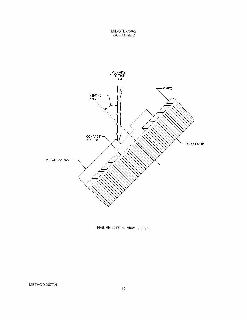
MIL-STD-750-2 w/CHANGE 2
METHOD 2077.4 12
FIGURE 2077–3. Viewing angle.
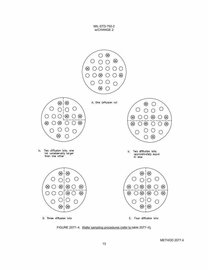
MIL-STD-750-2 w/CHANGE 2
METHOD 2077.4 13
FIGURE 2077–4. Wafer sampling procedures (refer to table 2077–II).

MIL-STD-750-2 w/CHANGE 2
METHOD 2077.4 14
FIGURE 2077–4. Wafer sampling procedures (refer to table 2077–II) – Continued.

MIL-STD-750-2 w/CHANGE 2
METHOD 2077.4 15
FIGURE 2077–5. Concept of reduction of cross-sectional area of metallization as accept/reject criteria (any combination of defects and thinning over a step which reduces the cross-sectional area of the metal to less than 50 percent of metal cross-sectional area as deposited on the flat surface, shall be cause for rejection).

MIL-STD-750-2 w/CHANGE 2
METHOD 2077.4 16
FIGURE 2077–6. Void near oxide step at 3,400X (accept).
FIGURE 2077–7. Voids at oxide step at 3,300X (reject).

MIL-STD-750-2 w/CHANGE 2
METHOD 2077.4 17
NOTE: Tunnel does not reduce cross-sectional area more than 50 percent.
FIGURE 2077–8. Tunnel/cave at oxide step at 10,000X (accept).
FIGURE 2077–9. Tunnel/cave at oxide step at 5,000X (reject).

MIL-STD-750-2 w/CHANGE 2
METHOD 2077.4 18
FIGURE 2077–10. Separation of metallization at oxide step at base contact at 10,000X (accept).
FIGURE 2077–11. Separation of metallization at contact step at 7,000X (reject)

MIL-STD-750-2 w/CHANGE 2
METHOD 2077.4 19
FIGURE 2077–12. Crack-like defect at oxide step at 20,000X (accept).
FIGURE 2077–13. Crack-like defect at oxide step at 7,000X (reject).

MIL-STD-750-2 w/CHANGE 2
METHOD 2077.4 20
FIGURE 2077–14. Acceptable thinning at oxide step with more than 50 percent of cross-sectional area remaining at step (multi-level-metal) at 7,200X.
FIGURE 2077–15. Unacceptable thinning at oxide step with less than 50 percent of cross-sectional area remaining at step (multi-level-metal) at 7,200X.

MIL-STD-750-2 w/CHANGE 2
METHOD 2077.4 21
FIGURE 2077–16. Steep oxide step (MOS) at 6,000X (accept).
FIGURE 2077–17. Steep oxide step (MOS) at 9,500X (reject).

MIL-STD-750-2 w/CHANGE 2
METHOD 2077.4 22
FIGURE 2077–18. Peeling or lifting of general metallization in contact window area at 5,000X (reject).
FIGURE 2077–19. General metallization voids at 10,000X (accept).
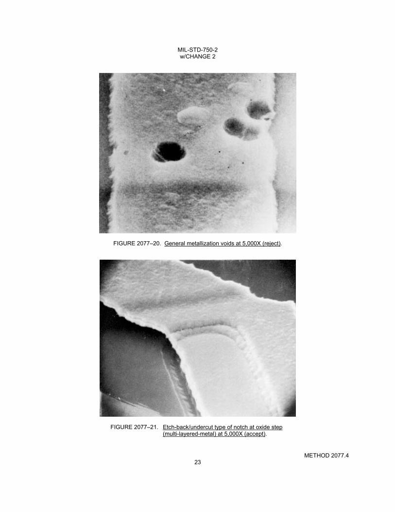
MIL-STD-750-2 w/CHANGE 2
METHOD 2077.4 23
FIGURE 2077–20. General metallization voids at 5,000X (reject).
FIGURE 2077–21. Etch-back/undercut type of notch at oxide step (multi-layered-metal) at 5,000X (accept).

MIL-STD-750-2 w/CHANGE 2
METHOD 2077.4 24
FIGURE 2077–22. Barrier or adhesion layer etch-back/undercut type of notch at oxide step (multi-layered-metal) at 5,000X (accept).

MIL-STD-750-2 w/CHANGE 2
This page is intentionally left blank.

MIL-STD-750-2 w/CHANGE 2
METHOD 2078 1 of 20
METHOD 2078
INTERNAL VISUAL FOR WIRE BONDED DIODES/RECTIFIERS
1. Purpose. The purpose of this test method is to verify the construction and workmanship of semiconductor devices utilizing junction passivated diode and rectifiers chips that use wire to chip technology. This test method will be performed prior to capping or encapsulation.
2. Apparatus. The apparatus for this inspection shall consist of the following:
a. Optical equipment capable of the specified magnifications. b. Light sources of sufficient intensity to adequately illuminate the devices being inspected. c. Adequate fixturing for handling the devices being inspected without causing damage. d. Adequate covered storage and transportation containers to protect devices from mechanical damage and
environmental contamination. e. Any visual standards (drawings and photographs) necessary to enable the inspector to make objective
decisions as to the acceptability of the devices being examined.
3. Definitions.
3.1 Glassivation. The top layer of transparent insulating material that covers the active circuit area metallization, but excludes the bond pads.
3.2 Passivation. Silicon oxide, nitride, or other insulating material that is grown or deposited directly on the die prior to the deposition of any metal.
4. Procedure.
4.1 General. The device shall be examined in a suitable sequence of observations within the specified magnification range to determine compliance with the requirements of this test method. It is optional that the chips used have passed test method 2073 of this standard prior to assembly.
4.1 Inspection control. Within the time interval between visual inspection and preparation for sealing, devices shall be stored in a controlled environment (one which controls airborne particle count and relative humidity). The use of an inert gas environment, such as dry nitrogen shall satisfy the requirements for storing in a controlled environment. Devices examined in accordance with this test method shall be inspected and stored in a class 100,000 environment, in accordance with ISO 14644–1 and ISO 14644–2, except that the maximum allowable relative humidity shall not exceed 65 percent (see 4.1.2).
4.1.2 Humidity control. If devices are subjected to a high temperature bake (> 100C) immediately prior to sealing, the humidity control is not required. Unless a cleaning operation is performed prior to sealing, devices shall be in covered containers when transferred from one controlled environment to another.
4.1.3 Magnification (see table 2078–I). High magnification inspection shall be performed perpendicular to the die surface with normal incident illumination. Low magnification inspection shall be performed with either a monocular, binocular, or stereo microscope, and the inspection performed within any appropriate angle, with the device under suitable illumination. The inspection criteria of 4.5 and 4.7.1 may be examined at "high magnification" at the manufacturer's option. High power magnification may be used to verify a discrepancy noted at a low power.
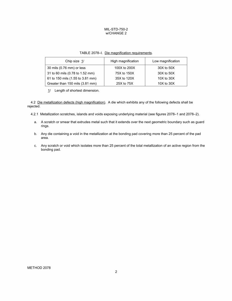
MIL-STD-750-2 w/CHANGE 2
METHOD 2078 2
TABLE 2078–I. Die magnification requirements.
Chip size 1/ High magnification Low magnification
30 mils (0.76 mm) or less 100X to 200X 30X to 50X
31 to 60 mils (0.78 to 1.52 mm) 75X to 150X 30X to 50X
61 to 150 mils (1.55 to 3.81 mm) 35X to 120X 10X to 30X
Greater than 150 mils (3.81 mm) 25X to 75X 10X to 30X
1/ Length of shortest dimension.
4.2 Die metallization defects (high magnification). A die which exhibits any of the following defects shall be rejected.
4.2.1 Metallization scratches, islands and voids exposing underlying material (see figures 2078–1 and 2078–2).
a. A scratch or smear that extrudes metal such that it extends over the next geometric boundary such as guard rings.
b. Any die containing a void in the metallization at the bonding pad covering more than 25 percent of the pad
area. c. Any scratch or void which isolates more than 25 percent of the total metallization of an active region from the
bonding pad.

MIL-STD-750-2 w/CHANGE 2
METHOD 2078 3
FIGURE 2078–1. Metallization scratches and voids.

MIL-STD-750-2 w/CHANGE 2
METHOD 2078 4
FIGURE 2078–2. Metallization scratches and voids – Continued.

MIL-STD-750-2 w/CHANGE 2
METHOD 2078 5
4.2.2 Metallization corrosion. Any metallization which shows evidence of corrosion.
4.2.3 Metallization adherence. Any metallization which has lifted, peeled, or blistered.
4.2.4 Metallization probing. Criteria contained in 4.2.1 shall apply as limitations on probing damage.
4.2.5 Metallization alignment.
a. Except by design, contact window that has less than 75 percent of its area covered by continuous metallization.
b. On metal overlay devices, any misalignment causing the metal to be extended to more than 50 percent of
the way to the next geometric boundary.
4.3 Passivation and diffusion faults (see figure 2078–3) (high magnification). A device which exhibits any of the following defects shall be rejected:
a. Any diffusion fault that allows bridging between any two diffused areas including field rings and guard rings or any two metallization strips.
b. Any passivation fault including pinholes not covered by glassivation that exposes semiconductor material
and allows bridging between any two diffused areas, any two metallization strips, or any such combination not intended by design.
c. Unless intended by design, a diffusion area which is discontinuous. d. On metal overlay devices, an absence of passivation visible at the edge and continuing under the
metallization causing an apparent short between the metal and the underlying material (closely spaced double or triple lines on the edges of the defect indicate that it may have sufficient depth to penetrate down to the silicon).
e. Except by design, any active junction not covered by passivation or glassivation.

MIL-STD-750-2 w/CHANGE 2
METHOD 2078 6
FIGURE 2078–3. Passivation and diffusion faults.
4.4 Sawing and die defects (see figures 2078–4 and 2078–5) (high magnification). A device which exhibits any of the following defects shall be rejected:
a. Unless by design, less than .1 mil (0.0025 mm) passivation visible between active metallization or bond pad periphery and the edge of the die.
b. Any chip-out or crack extending to within 1.0 mil (0.025 mm) of a diffusion boundary. c. Die having attached portions of the active area of another die. d. Any crack which exceeds 2.0 mils (0.051 mm) in length inside the scribe grid or scribe line that points toward
active metallization or active area and extends into the oxide area. e. Any crack or chip-out that extends to any active metallization area.

MIL-STD-750-2 w/CHANGE 2
METHOD 2078 7
f. Any chip-out which extends to a guard ring.
FIGURE 2078–4. Cracks and chips.

MIL-STD-750-2 w/CHANGE 2
METHOD 2078 8
FIGURE 2078–5. Cracks and chips (continued).

MIL-STD-750-2 w/CHANGE 2
METHOD 2078 9
4.5 Bond inspection (low magnification). This inspection and criteria shall be the required inspection for the bond type(s) and location(s) to which they are applicable when viewed from above (see figures 2078–6 and 2078–7). Wire tail is not considered part of the bond when determining physical bond dimensions. A device, which exhibits any of the following defects, shall be rejected.
4.5.1 Gold ball bonds.
a. Gold ball bonds on the die or package post where the ball bond diameter is less than 2.0 times or greater than 5.0 times the wire diameter.
b. Gold ball bonds where the wire exit is not completely within the periphery of the ball. c. Gold ball bonds where the exiting wire is not within the boundaries of the bonding pad. d. Any visible intermetallic formation at the periphery of any gold ball bond.
4.5.2 Wedge bonds.
a. Ultrasonic wedge bonds on the die or package post that are less than 1.2 times or greater than 3.0 times the
wire diameter in width, or are less than 1.5 times or greater than 5.0 times the wire diameter in length. b. Thermo compression wedge bonds on the die or package post that are less than 1.2 times or greater than
3.0 times the wire diameter in width or are less than 1.5 or greater than 5.0 times the wire diameter in length.
4.5.3 Stitch wire bonds. A stitch wire bond, usually done with a wedge bonder, is where a single bond wire has 2 or more bonds along its length to the chip. These can be evaluated using the criteria for single wedge bonds with the following guidelines:
a. The bond closest to the wire end should meet all the criteria of a single bond except there is no cutoff tail
requirement. b. The bond farthest from the wire end must meet the cutoff tail requirement. c. Wire rise clearance criteria between bonds is waived. d. Shape and deformation criteria of each bond is the same as for a single bond.
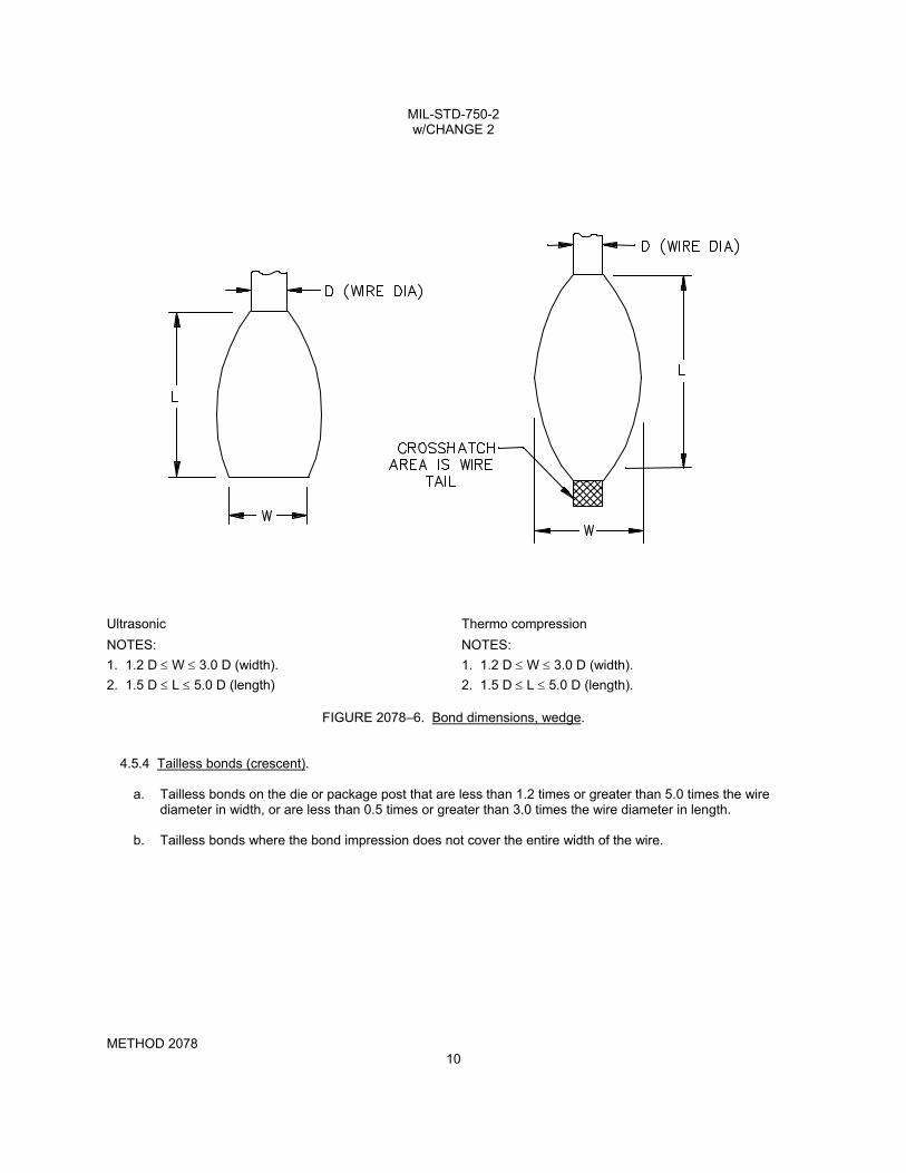
MIL-STD-750-2 w/CHANGE 2
METHOD 2078 10
Ultrasonic Thermo compression
NOTES: NOTES:
1. 1.2 D W 3.0 D (width). 1. 1.2 D W 3.0 D (width).
2. 1.5 D L 5.0 D (length) 2. 1.5 D L 5.0 D (length).
FIGURE 2078–6. Bond dimensions, wedge.
4.5.4 Tailless bonds (crescent).
a. Tailless bonds on the die or package post that are less than 1.2 times or greater than 5.0 times the wire diameter in width, or are less than 0.5 times or greater than 3.0 times the wire diameter in length.
b. Tailless bonds where the bond impression does not cover the entire width of the wire.

MIL-STD-750-2 w/CHANGE 2
METHOD 2078 11
NOTES: 1. 1.2.D ≤ W ≤ 5.0 D (width). 2. 0.5 D ≤ L ≤ 3.0 D (length).
FIGURE 2078–7. Bond dimensions, tailless or crescent.
4.5.5 General (gold ball, wedge, and tailless). As viewed from above, a device which exhibits any of the following defects shall be rejected:
a. Bonds on the die where less than 75 percent of the bond is within the unglassivated bonding pad area (except where due to geometry, the bonding pad is smaller than the bond, the criteria shall be 50 percent).
b. Wire bond tails that extend over and make contact with any metallization not covered by glassivation and not
connected to the wire. c. Wire bond tails (pigtails) that exceed two wire diameters in length at the bonding pad or four wire diameters
in length at the package post (see figure 2078–8). d. Bonds on the package posts that are not bonded entirely on the flat surface of the post top. e. A bond on top of another bond. f. Bonds placed so that the separation between bonds and adjacent glassivated die metallization is less than
.25 mil (0.006 mm) or the separation between adjacent bonds is less than .25 mil (0.006 mm). This criteria does not apply to designs which employ multiple bond wires in place of a single wire.
i. Bonds located where any of the bond is placed on an area containing die preform mounting material. j. For aluminum wires over 2.0 mils (0.051 mm) diameter, the bond width shall not be less than 1.0 times the
wire diameter.

MIL-STD-750-2 w/CHANGE 2
METHOD 2078 12
FIGURE 2078–8. Pigtail length.
4.6 Internal lead wires (low magnification). This inspection and criteria shall be required inspection for the location(s) to which they are applicable when viewed from above. A device which exhibits any of the following defects shall be rejected:
a. Any wire that comes closer than two wire diameters or 5.0 mils (0.127 mm), whichever is less, to unglassivated operating metallization, another wire (common wires and pigtails excluded) package post, unpassivated die area, or any portion of the package, including the plane of the lid to be attached. (Within a 5.0 mil (0.127 mm) spherical radial distance from the perimeter of the bond on the die surface, the separation can be 1.0 mil (0.025 mm).)
b. Nicks, tears, bonds, cuts, crimps, scoring, or neckdown in any wire that reduces the wire diameter by more
than 25 percent. See figure 2078–9. c. Missing or extra lead wires. d. Bond lifting or tearing at interface of pad and wire. e. Any wire which runs from die bonding pad to package post and has no arc or stress relief
(see figure 2078–10). f. Except in common connectors, wires which cross other wires. g. Wire(s) not in accordance with bonding diagram (see figure 2078–11). h. Wire is kinked (unintended sharp bend) with an interior angle of less than 90 degrees or twisted to an extent
that stress marks appear.

MIL-STD-750-2 w/CHANGE 2
METHOD 2078 13
i. Wire (ball bonded devices) not within 10 degrees of the perpendicular to the surface of the chip for a distance of greater than 0.5 mil (0.013 mm) before bending toward the package post or other termination point.
j. Excessive lead burn at lead post weld. k. Pigtail longer than 4 times the wire diameter (see figure 2078–8). l. A bow or loop between double bonds at post greater than four times wire diameter. m. Excessive loops, bows, or sags in any wire such that it could short to another wire, to another pad, to
another package post, to the die or touch any portion of the package. n. When clips are used, solder fillets shall encompass at least 50 percent of the clip-to-die and post-to-clip
periphery. There shall be no deformation or plating defects on the clip.
FIGURE 2078–9. Unacceptable wirebond neckdown.

MIL-STD-750-2 w/CHANGE 2
METHOD 2078 14
FIGURE 2078–10. Wire bond stress relief.
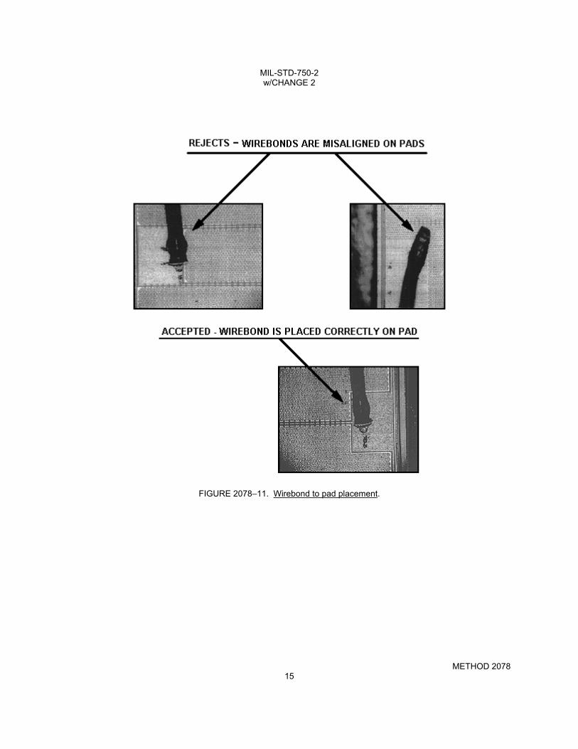
MIL-STD-750-2 w/CHANGE 2
METHOD 2078 15
FIGURE 2078–11. Wirebond to pad placement.
MIL-STD-750-2 w/CHANGE 2
METHOD 2078 16
4.7 Package conditions (magnification as indicated). A device which exhibits any of the following defects shall be rejected.
4.7.1 Conductive foreign material on die surface. All foreign material or particles may be blown off with a nominal gas blow (approximately 20 psi (138 kPa)) or removed with a soft camel hairbrush. The device shall then be inspected for the following reject criteria (low magnification):
a. Loosely attached foreign particles (conductive particles which are attached by less than one-half of their largest dimension), which are present on the surface of the die that are large enough to bridge the narrowest unglassivated metal spacing (silicon chips shall be included as conductive particles).
b. Embedded foreign particles on the die that bridge two or more metallization paths or semiconductor
junctions, or any combination of metallization or junction. c. Liquid droplets, chemical stains, or photoresist on the die surface that bridge any combinations of
unglassivated metal or bare silicon areas. d. Ink on the surface of the die that covers more than 25 percent of a bonding pad area or that bridges any
combination of unglassivated metallization or bare silicon areas.
4.7.2 Die mounting (low magnification).
a. Die mounting material buildup that extends onto the top surface of the die or extends vertically above the top surface of the die and interferes with bonding.
b. Die to header mounting material which is not visible around at least three complete sides or 75 percent of
the die perimeter. Wetting criteria is not required if the devices pass an approved electrical die attach evaluation test.
c. Any flaking of the die mounting material. d. Any balling of the die mounting material which does not exhibit a fillet when viewed from above.
4.7.3 Die orientation.
a. Die is not located or orientated in accordance with the applicable assembly drawing of the device. b. Die is visibly tipped or tilted (more than 10 degrees) with respect to the die attach surface.
4.7.4 Internal package defects (low magnification inspection) (applicable to headers, bases, caps, and lids).
a. Any header or post plating which is blistered, flaked, cracked, or any combination thereof. b. Any conductive particle which is attached by less than one-half of the longest dimension. c. A bubble or a series of interconnecting bubbles in the glass surrounding the pins which are more than
one-half the distance between the pin and body or pin-to-pin. d. Header posts which are severely bent. e. Any glass, die, or other material greater than 1.0 mil (0.025 mm) in its major dimension which adheres to the
flange or side of the header and would impair sealing.
MIL-STD-750-2 w/CHANGE 2
METHOD 2078 17
f. Any stain, varnish, or header discoloration which appears to extend under a die bond or wire bond. g. For isolated stud packages:
(1) Any defect or abnormality causing the designed isolating paths between the metal island to be reduced
to less than 50 percent of the design separation. (2) A crack or chip-out in the substrate.
4.7.5 Presence of extraneous matter. Extraneous matter (foreign particles) shall include, but not be limited to:
a. Any foreign particle, loose or attached, greater than 3. mil (0.08 mm) or of any lesser size which is sufficient
to bridge non-connected conducting elements of the device. b. Any wire tail extending beyond its normal end by more than two diameters at the semiconductor die pad or
by more than four wire diameters at the package post (see figure 2078–11). c. Any burr on a post (header lead) greater than 3.0 mil (0.08 mm) in its major dimension or of such
configuration that it may break away. d. Excessive semiconductor die bonding material buildup (see figures 2078–12 and 2078–13). A
semiconductor die shall be mounted and bonded so that it is not tilted more than 10 degrees from mounting surface. The bonding agent that accumulates around the perimeter of the semiconductor die and touches the side of the semiconductor die shall not accumulate to a thickness greater than that of the semiconductor die. Where the bonding agent is built up but is not touching the semiconductor die, the build up shall not be greater than twice the thickness of the semiconductor die. There shall be no excess semiconductor die bonding material in contact with the active surface of the semiconductor die or any lead or post, or separated from the main bonding material area.
e. Flaking on the header or posts or anywhere inside the case. f. Extraneous ball bonds anywhere inside case, except for attached bond residue when re-bonding is allowed.
4.8 Glassivation and silicon nitride defects (high magnification). No device shall be acceptable that exhibits any of
the following defects:
a. Glass crazing that prohibits the detection of visual criteria contained herein. b. Any glassivation which has delaminated. (Lifting or peeling of the glassivation may be excluded from the
criteria above, when it does not extend more than 1.0 mil (0.025 mm) distance from the designed periphery of the glassivation, provided that the only exposure of metal is adjacent to bond pads or of metallization leading from those pads.)
c. Except by design, two or more adjacent active metallization paths which are not covered by glassivation. d. Glassivation which covers more than 25 percent of the design bonding pad area.

MIL-STD-750-2 w/CHANGE 2
METHOD 2078 18
4.9 Post organic protective coating visual inspection. If devices are to be coated with an organic or silicone protective coating, the devices shall be visually examined in accordance with the criteria specified in 4.1 prior to application of the coating. After the application and cure of the organic protective coating the devices shall be visually examined under a minimum of 10X magnification. Devices, which exhibit any of the following defects, shall be rejected:
a. Except by design, any unglassivated or unpassivated areas or insulating substrate which has incomplete coverage.
b. Open bubbles, cracks or voids in the organic protective coating. c. A bubble or a chain of bubbles which covers two adjacent metallized surfaces. d. Organic protective coating, which has flaked or peeled. e. Organic protective coating, which is tacky. f. Conductive particles, which are embedded in the coating and are large enough to bridge the narrowest
unglassivated active metal spacing (silicon chips shall be included as conductive particles).
5. Summary. The following conditions shall be specified in the applicable performance specification sheet or acquisition document:
a. Detailed requirements for materials, design, construction, and workmanship. b. Magnification requirements, if other than specified herein.

MIL-STD-750-2 w/CHANGE 2
METHOD 2078 19
DETAIL A
NOTE: Die and wire are not necessarily visible.
FIGURE 2078–12. Extraneous bonding material build-up.

MIL-STD-750-2 w/CHANGE 2
METHOD 2078 20
FIGURE 2078–13. Acceptable and unacceptable excess material.

MIL-STD-750-2 w/CHANGE 2
METHOD 2081 1 of 1
METHOD 2081
FORWARD INSTABILITY, SHOCK (FIST)
1. Purpose. This test method is intended to detect any semiconductor device discontinuity "ringing" or shifting of the forward dc voltage characteristic monitored during shock.
2. Apparatus. The shock testing apparatus shall be capable of providing shock pulses of the specified peak acceleration and pulse duration to the body of the device. The acceleration pulse, as determined from the unfiltered output of a transducer with a natural frequency greater than or equal to five times the frequency of the shock pulse being established, shall be a half-sine waveform with an allowable distortion not greater than ±20 percent of the specified peak acceleration. The pulse duration shall be measured between the points at 10 percent of the peak acceleration during rise time and at 10 percent of the peak acceleration during decay time. Absolute tolerances of the pulse duration shall be the greater of ±0.6 ms or ±15 percent of the specified duration for specified durations of 2 ms and greater. For specified durations less than 2 ms, absolute tolerances shall be the greater of ±0.1 ms or ±30 percent of the specified duration. The monitoring equipment shall be an oscilloscope or any "latch and hold" interrupt detector of appropriate sensitivity.
3. Procedure. The shock testing apparatus shall be mounted on a sturdy laboratory table or equivalent base and leveled before use. The device shall be rigidly mounted or restrained by its case with suitable protection for the leads. Special care is required to ensure positive electrical connection to the device leads to prevent intermittent contacts during shock. The device shall be subjected to five shock pulses of 1,000 g peak minimum for the pulse duration of 1 ms in each of two perpendicular planes. For each blow, the carriage shall be raised to the height necessary for obtaining the specified acceleration and then allowed to fall. Means may be provided to prevent the carriage from striking the anvil a second time. With the specified dc voltage and current applied, the forward dc characteristic shall be displayed on a oscilloscope swept at 60 Hz and shall be monitored continuously during the shock test.
4. Failure criteria. During the shock test, any discontinuity, flutter, drift, or shift in oscilloscope trace or any dynamic instabilities shall be cause for rejection of the device.
5. Summary. The following conditions shall be specified in the applicable performance specification sheet or acquisition document:
a. Acceleration and duration of pulse, if other than that specified (see 3). b. Number and direction of blows, if other than that specified (see 3). c. Electrical-load conditions (see 3).

MIL-STD-750-2 w/CHANGE 2
METHOD 2081 1 of 1
This page is intentionally left blank.
MIL-STD-750-2 w/CHANGE 2
METHOD 2082 1 of 1
METHOD 2082
BACKWARD INSTABILITY, VIBRATION (BIST)
1. Purpose. This test method is intended to detect any semiconductor device discontinuity "ringing" or shifting of the reverse dc voltage characteristic monitored during vibration.
2. Apparatus. The vibration testing apparatus shall be capable of providing the required frequency vibration at the specified levels. The monitoring equipment shall be an oscilloscope or any "latch and hold" interrupt detector of appropriate sensitivity.
3. Procedure. The device shall be rigidly fastened on the vibration platform. Special care is required to ensure positive electrical connection to the device leads to prevent intermittent contacts during vibration. Care must also be exercised to avoid magnetic fields in the area of the device being vibrated. The device shall be vibrated with a simple harmonic motion at 60 ±3 Hz, with .1 inch (2.54 mm) minimum double amplitude displacement for a period of 30 seconds minimum in the X orientation planes (see note below). The acceleration shall be monitored at a point where the "g" level is equivalent to that of the support point for the device(s). With the specified dc voltage and current applied (for zeners only) and with the specified reverse dc voltage applied (for diodes and rectifiers only), the reverse dc characteristic shall be displayed on an oscilloscope swept at 60 Hz and shall be monitored continuously during the vibration test.
NOTE: g level calculation:
g = .0512f2DA. f = frequency in Hz. DA = double amplitude in inches.
4. Failure criteria. During the vibration test, any discontinuity, flutter, drift, or shift in oscilloscope trace or any
dynamic instabilities shall be cause for rejection of the device.
5. Summary. The following conditions shall be specified in the applicable performance specification sheet or acquisition document:
a. Frequency range and time period, if other than that specified. b. Peak acceleration, if other than that specified. c. Orientation plan, if other than that specified. d. Voltage and lead conditions.

MIL-STD-750-2 w/CHANGE 2
This page is intentionally left blank.

MIL-STD-750-2 w/CHANGE 2
METHOD 2100 1 of 6
METHOD 2100
X–RAY FLUORESCENCE (XRF) SCAN LOCATIONS FOR DISCRETE SEMICONDUCTOR
TIN – LEAD CONTENT ANALYSIS
1. Purpose. This test method establishes the XRF scan locations, guidance, and sampling plans for the semiconductor device package styles shown. XRF can reliably make an accurate determination of a material’s Tin–Lead (Sn–Pb) content only when the design and construction of the sample is known. The design and construction of the test sample being subjected to XRF shall be made available to test personnel for reference. Further details may be found in JEDEC JESD213.
1.1 Definitions.
1.1.1 Alignment. The adjustment of an object in relation with other objects, or a static orientation of an object or set of objects in relation to others.
1.1.2 Focusing. The action of directing rays toward a point where the rays converge.
1.1.3 Beam collimation. The process of restricting and confining an x–ray beam to a given area.
1.1.4 Scanning Electron Microscopy-Energy Dispersive Spectroscopy (SEM-EDS). Measures the number of x–rays produced by a solid sample when irradiated by electrons versus the energy of these x–rays.
1.1.5 Spatial resolution. The minimum distance between two adjacent features of the minimum size of a feature, that can be detected by a remote sensing system.
1.1.6 X–ray fluorescence (XRF). The process of emissions of characteristic x–rays.
2. Apparatus. The apparatus for this test method shall consist of the following:
a. XRF Instrumentation capable of qualitatively identifying the metal present in a complex sample and providing quantitative accuracy sufficient to ensure a minimum of 3.0 percent Pb. The alignment and focusing system shall provide visual identification of the surface being analyzed. The spatial resolution of the instrument must be sufficient to identify the material composition of the area under analysis, excluding adjacent materials. This requires an x–ray beam smaller than the surface being analyzed, or a technique that provides materials surrounding the surface being analyzed do not contain prohibited materials. The spatial resolution of the instrument must be verified annually.
b. An x–ray detector with sufficient resolution to quantify Pb to within ±2 wt percent accuracy, in the range of 0
to 10 wt percent, in combination with interfering energy lines from other elements (such as Bismuth, Bi). Proportional counters shall not be used. The excitation voltage for x–rays shall be 40keV (minimum) to support detection of higher energy lines.
c. Positioning fixtures or sample trays which are made of materials that do not interfere with the accuracy of
the analysis, e.g., pure commercial grade aluminum. d. Verification standards with a Sn-Pb composition standard with a Pb content of 3.0 wt percent. This
verification standard shall be a cast alloy sample made from high purity Sn and Pb and must be NIST traceable.

MIL-STD-750-2 w/CHANGE 2
METHOD 2100 2
3. Procedure.
3.1 Verification. The equipment calibration shall be verified at the beginning of each work shift by measuring the Sn-Pb reference material. The result must agree with the assigned value for the reference material after taking into account the uncertainty of the assigned value and the laboratory’s uncertainty. (i.e., if a 3.0 wt percent Pb standard has a tolerance of ±10 percent, the allowable range would be 2.7 to 3.3 wt percent Pb.) A control chart to monitor this comparison shall be implemented.
3.2 Scanning. Each visually identifiable component metal surface requires a separate scan; for example, metal device leads, cans, and lids all require individual scans. The analysis of frit/header glass shall be avoided as the detection of Pb in these material(s) can provide false Pb indications.
3.3 Sampling. The sampling plan shall be specified in the applicable acquisition document.
3.4 Measurements. Each sample shall be measured independently. Scanning multiple samples under the x–ray beam at one time is not acceptable. The samples should be measured on a flat surface, when possible.
3.5 Acceptance criteria. The samples shall pass if each of the measured readings are greater than or equal to 3.0 wt percent Pb. One rejected sample shall be cause of rejection for the entire sample lot. A failed lot can be reworked in accordance with the requirements of MIL–PRF–19500.
4. Scan locations and guidance. Figures 2100–1 through 2100–6 show typical scan locations for the most common package styles. Each visually identifiable device metal surface requires a separate scan. For example, device metal leads, cans, and lids all require individual scans. Flat surfaces provide the greatest measurement accuracy. Sharp edges, highly curved surfaces, and locations that will mix responses from dissimilar materials will result in lower accuracy. For non-flat or rounded surfaces, the sample shall be measured at the center to prevent extending beyond the sample edge. Caution should be exercised to prevent x–ray beam scatter when taking measurements on non-flat or rounded surfaces.
4.1 Scan locations on device leads. Leaded devices shall be measured as closely as practical to the device body, with care to exclude the body material. A second location away from the device body shall also be measured.
4.2 Scan locations on large or rounded surfaces. Devices with varied geometry shall be measured at each different plane. In all cases, the x–ray spot or beam size shall be small enough to remain within the area under test with a guard band area approximating the beam diameter. Large pad devices shall be scanned in one location with adequate scan size to meet accuracy and reproducibility requirements, rather than scanning the entire surface (see figure 2100–1).
5. Summary. The following conditions shall be specified by the applicable performance specification sheet or acquisition document:
a. The sample size, if different than specified herein. b. The composition of Sn-Pb to be identified, if different than specified herein.

MIL-STD-750-2 w/CHANGE 2
METHOD 2100 3
FIGURE 2100–1. Typical scan location on flat surface mounted devices.
FIGURE 2100–2. Scan locations on can style package.
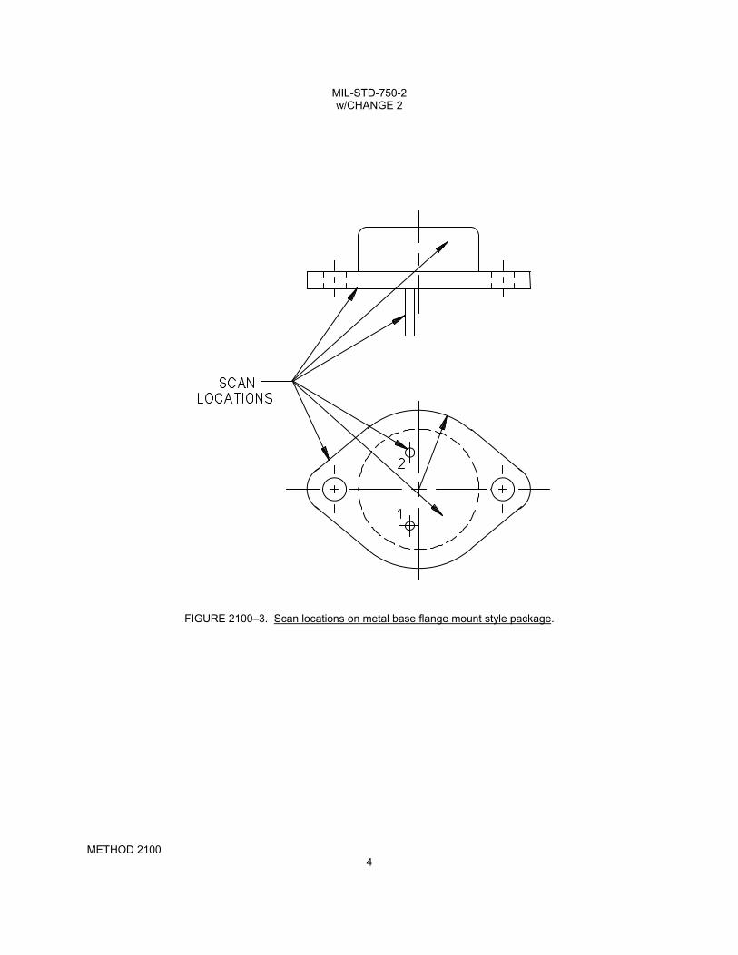
MIL-STD-750-2 w/CHANGE 2
METHOD 2100 4
FIGURE 2100–3. Scan locations on metal base flange mount style package.

MIL-STD-750-2 w/CHANGE 2
METHOD 2100 5
FIGURE 2100–4. Scan locations on glass, axial leaded package style.
FIGURE 2100–5. Scan locations – ceramic, metal sealed, single in-line package.

MIL-STD-750-2 w/CHANGE 2
METHOD 2100 6
FIGURE 2100–6. Scan locations on metal electrode face (MELF) style package.

MIL-STD-750-2 w/CHANGE 2
METHOD 2101.3 1 of 8
METHOD 2101.3
DESTRUCTIVE PHYSICAL ANALYSIS FOR DIODES
1. Purpose. This test method describes detail procedures and evaluation guidelines for the destructive physical analysis (DPA) of commonly specified diodes. It is intended to provide techniques for determining compliance with specified construction requirements, as well as for evaluating processes, workmanship, and material consistency of the diode in relation to MIL–PRF–19500 requirements.
2. Scope. This test method pertains to all diode constructions including metal can, except where the die is encapsulated in a package normally specified for transistors. Diodes in transistor packages shall be evaluated using test method 2102 of this standard.
3. Requirements.
3.1 Apparatus. Equipment requirements shall be as specified in the various test methods for each procedure listed. Equipment for delidding will vary from package to package and may be custom built or provided commercially.
3.2 Sampling. Sampling for DPA shall be as specified in the applicable performance specification sheet or acquisition document requirements, by contract. Destructive analysis shall be totally compliant with the performance specification sheet for electrical and mechanical requirements or as otherwise specified in the acquisition document.
4. Procedure. The DPA samples shall be subjected to all procedures specified by the contract which are applicable to the device construction. The organization (contractor, subcontractor, or independent test lab) conducting the DPA test should contact the manufacturer of the device and supply a list of test methods to be used during DPA test.
a. If a device does not conform to the specific requirements herein, or contains systemic anomalies known to directly affect reliability, the disposition of the lot shall be according to contract. The manufacturer should be notified when anomalies occur, prior to continuing to the next DPA test, in order to address the findings in real time and propose any recommendations.
b. Random anomalies detected when devices are subjected to tests or examinations which are additional, or
more rigorous than those in the performance specification sheet, for the product assurance level being inspected, shall be noted in the report but shall not cause the lot to be considered non-conforming.
4.1 General. DPA status shall be completely documented in a report containing the following required information:
a. PIN and MIL–PRF–19500 reliability level. b. Device manufacturer. c. Lot date code. d. When applicable and where acquired, an order. e. Sample size for each test. f. Results of each test. g. Stamp or signature of analyst for each test. h. Shipment quantity represented by the DPA. i. Radiographs, one of each required view. j. PIND, sample size, and results.

MIL-STD-750-2 w/CHANGE 2
METHOD 2101.3 2
k. Photographs including one of entire dice excluding leads. l. One copy of electrical data. m. One copy of all mechanical dimensions data. n. When applicable, the test method number from this standard. o. Destruct sample evidence will remain with lot.
TABLE 2101–I Mandatory procedures. 1/
Techniques See
Electrical testing in accordance with group A, subgroup II of the performance specification sheet
4.3
Electrical testing in accordance with group A, subgroups III and IV and design ratings
4.4
External visual 4.5
Radiographic inspection 4.6
Hermetic seal 4.7
Hermetic seal for polymeric encapsulated devices such as bridge assemblies which contain hermetically sealed diodes shall be performed after the removal of the encapsulant
4.8 and 5.4
PIND testing 4.9
Residual gas analysis 4.10
For transparent diodes, internal visual inspection 4.11
Axial lead tensile test 4.12
Resistance to solvents 4.13
Solderability 4.14
Terminal strength 4.15
Decap analysis 5
1/ A list of techniques to be tailored for DPA performance according to the end item mission requirements and appropriate to the device construction. The tests required from this list shall be specified in the contract.
4.2 Tests. For MIL–PRF–19500 products, the test methods specified herein shall be performed by specific MIL–PRF–19500 qualified manufacturers, their customers, or approved sources appearing on the DLA Land and Maritime laboratory suitability list.

MIL-STD-750-2 w/CHANGE 2
METHOD 2101.3 3
4.3 Electrical and mechanical verification.
a. Group A, subgroup 2 inspections for room temperature dc tests shall be performed prior to DPA to verify electrical compliance of the sample. Variables data shall be taken and remain as part of the record for the lot.
b. Package dimensions as described in the outline drawing shall be measured and recorded when required.
Variables data from incoming or source inspection may be used to satisfy certain requirements of this procedure if the requirements of 4.2 herein are met and the contracting parties are in agreement.
4.4 Optional electricals. Optional electrical tests such as group A, subgroup 3 of MIL–PRF–19500 for high and low
temperature and subgroup 4 for dynamic characteristics may be performed. Additional design capability tests from the performance specification sheet, such as surge current, transient thermal resistance, and temperature coefficient may be performed. These will be specified by the contract.
4.5 External visual. External visual and mechanical examination shall be performed according to test method 2071 of this standard. All text on the device body shall be recorded. If the identifier BeO is found, the manufacturer shall be contacted for information regarding alternative decap techniques.
4.6 Radiography inspection. Radiographic inspection shall be performed in accordance with test method 2076 of this standard.
4.7 Hermetic seal. Hermetic seal testing shall be performed. Devices shall be subject to gross and fine leak in accordance with test method 1071 of this multipart test method standard. Gross leak conditions C and D are strictly prohibited. Any devices previously tested with fluorocarbon leak test fluid shall only be re-tested in accordance test method 1071 of this multipart test method standard, paragraph 17.d. Omit the fine leak requirement for double plug construction type diodes. Substitute gross leak, condition E, as applicable, for double plug types and test method 2068 of this standard for double plug opaque glass body types. Paint shall be removed prior to subjecting glass devices to hermetic seal evaluations.
4.8 Hermetic seal for polymeric encapsulated devices. Hermetic seal for polymeric encapsulated devices such as bridge assemblies, which contain hermetically sealed diodes, shall have the diodes evaluated after removal of the encapsulant (see 5.4 herein).
4.9 PIND. PIND testing shall be performed on devices with internal die cavities to condition A of test method 2052 of this standard.
4.10 Water vapor testing. Water vapor testing to test method 1018 of this multipart test method standard shall be performed on additional unopened devices to one of the three allowed procedures if it has been determined after delidding (see 5.3 herein) that corrosion or potentially corrosive elements such as chlorine or potassium salts are present in the cavity.
4.11 Internal visual. Internal visual inspection shall be performed prior to any destructive procedures for diodes of clear glass construction. Criteria shall be in accordance with test method 2074 of this standard. Opaque or metal can construction shall be evaluated for internal features after the decap procedure (see 5 herein).
4.12 Axial lead tensile strength. Axial lead tensile strength shall be tested in accordance with test method 2005 of this standard.
4.13 Resistance to solvents. Resistance to solvents shall be performed in accordance with test method 1022 of this multipart test method standard.
4.14 Solderability. Solderability shall be performed on "as received" devices within 30 days of receipt according to test method 2026 of this standard. Care in handling shall be exercised to prevent lead surface contamination prior to and during this test.
MIL-STD-750-2 w/CHANGE 2
METHOD 2101.3 4
4.15 Terminal strength. Terminal strength shall be performed in accordance with test method 2036 of this
standard.
5. Decap analysis. Decapping techniques for die inspection and die bond analysis shall be performed. (All inspections requiring an intact diode shall be completed at this point.)
5.1 Axial lead or surface mount construction.
a. The diode shall be encapsulated longitudinally in a mounting compound suitable for use as a carrier for further sample processing. The mounting compound will be selected to have expansion and contraction properties as close as possible to the device body encapsulant to prevent the generation of stress cracks in sample preparation.
b. For clear glass construction the sample shall be positioned in such a way that one side of the die is parallel
to the sectioning apparatus (see figure 2101–1). This will assure that polishing of the cross section will reveal areas from which approximate dimensions may be determined.
c. The sample shall be sectioned using a laboratory grade grinding and lapping table. Precautions shall be
taken to prevent damage to the sample by overly aggressive grit paper selection. In the case of cavity type constructions, the process of grinding shall stop immediately upon opening the cavity to allow for the insertion and curing of clear backfilling compound material. This is done to assure that the internal constituents of the assembly are encased and protected from damage to the die as the grinding process continues.
d. The DPA sample may be polished and stained to enhance construction details at one or several planes.
The specimen will be recorded by photomicroscopy when it is determined that the center of the die has been reached (see figure 2101–1). Two photographs will be taken; one containing means for dimensioning the image, or the optical magnification shall be indicated.
e. Due to the brittle characteristics of the various materials in the construction method, damage may be
induced by the sectioning technique. For glass diodes with metallurgical bond, die, or glass cracks, damage may be induced as the compression built into the seal is relaxed as the structure is weakened in the cross sectioning process. This method may not be used for disposition of metallurgical bond voids, however thermal impedance may be substituted for this method to validate the integrity of die attach.
f. Cracks or chip-outs found on the opposite side of the die active area are acceptable as long as they meet
the die criteria of test methods 2073 and 2074, of this standard.
5.2 Scribe, break and dig method for glass axial lead and surface mount types.
a. In this method the device is deliberately destroyed to allow visibility to the die attachment area. b. The diode body is scored circumferentially at the location of the die plane (see figure 2101–2). This is
usually accomplished with a diamond scribe. The device is then snapped into two pieces. (Observe eye protection against glass particles). Alternatively the glass body may be chemically dissolved and the die snapped (provided the die and die metallization are not attacked by the chemical that can be a common problem with this alternative). At this time the two plug surfaces may be inspected for both silicon and die metallization residue.
c. The silicon remaining on each plug may be chemically removed to provide visibility to the attachment
interface materials or by further scraping or digging through all of the bond interfaces; however, this step is not mandatory. Photographs will be taken of both separated attachment surfaces. A means may be provided in the photo to dimension the image.
*

MIL-STD-750-2 w/CHANGE 2
METHOD 2101.3 5
5.2.1 Die bond evaluation. Metallurgically bonded construction types shall be evaluated to the requirements of A.3.19 of MIL–PRF–19500. Both separated contact interfaces shall be optically evaluated for the bond area in accordance with table 2101–II (die attach criteria).
TABLE 2101–II. Die attach criteria.
Construction Percent design contact area
to be bonded (typical)
Category I: Eutectic, thermally matched 80
Category II: Solder 50
Silver button with braze 1/ 25
Category III: Silver button side Unspecified
Back side 2/ 10 Category III: Low voltage Zeners and
Schottky devices as applicable 3/
0 (Pressure bonds)
1/ Dumet silver button design contact area is the entire button top view area in intimate contact with the plug or braze preform interface. When both sides of the die are adequately bonded, the button to silicon interface (the area from which silver has grown, but not including any area which may be expanded over protective oxides) may become the area where separation occurs using the scribe and break technique to open the glass. The button to silicon interface will then become the measured design contact area. The percent bond area will be determined by the silicon pulled and remaining on the backside of the button.
2/ Dumet silver button construction: The percent area requirement applies only to the back contact or silicon side. The button to plug interface shall be bonded at point of contact or the tangent formed at their interface.
3/ The requirements of 5.2.1 do not apply for thermally matched non-cavity category III construction.
NOTE: If a device does not satisfy the die attach criteria, as specified, thermal impedance testing (Method 3101 of MIL-STD-750) already performed during 100% screening shall be used as a basis to establish acceptability for use. If device serialization is required, the manufacturer shall show evidence of the device thermal impedance testing results.
For transient voltage suppressors (TVSs), clamping voltage testing shall be used in lieu of
thermal impedance testing for bipolar devices or when thermal impedance testing is not required in the specification sheet.
*

MIL-STD-750-2 w/CHANGE 2
METHOD 2101.3 6
5.3 Stud mount or axial lead metal can.
a. Determine internal construction techniques from construction documentation or radiographic inspection. b. For crimp construction, encapsulate one device in a specimen mounting compound suitable for grinding,
lapping, and polishing procedures. Section the crimp perpendicular to the longitudinal axis to the point where the crimp is made (as determined from the construction details in the drawings or radiographic image) and determine the quality of the mechanical attachment process (see figure 2101–3).
c. This same sample may be used to observe the construction and dimensions of the internal elements. This
will be accomplished by cross section of the device along the longitudinal axis and backfilling the internal cavity with epoxy as soon as the case is penetrated to prevent damage in the grinding operations to follow. Section the device to the approximate center of the die by carefully examining the device at various planes and reducing the grit abrasiveness to limit sectioning damage. Polish and stain the sample to enhance die construction. Then photograph the internal elements.
d. To view all internal surfaces, unmounted samples shall be delidded by cutting the crimp terminal just below
the mechanical attachment then removing the lid by cutting circumferentially with a delidding device above the seating flange (see figure 2101–3). Care must be taken to prevent damage to the post connection at the top of the die when delidding.
e. The device shall be evaluated for die attachment position, die to preform and header interface, die
topography, and post or "C" bend attachment. Photographs of internal construction will be made.
f. Bond strength testing using test method 2037 of this standard is optional for construction with metal clips or wires.
g. When practical, die shear or punch testing for metal cans shall be in accordance with test method 2017 of
this standard.
5.4 Plastic encapsulated assemblies.
a. Complex devices such as bridges containing several discrete devices shall be evaluated externally for all major features as applicable and described above for individual devices.
b. Internal construction shall be evaluated by removing the device encapsulating material with appropriate
reagents using standard laboratory practice. Where uncertainty about the destructiveness of chemicals exists on internal construction elements, experiments on electrical rejects should occur or the manufacturer should be contacted for guidance.
c. Individual diode placement and method of attachment to assembly terminals shall be evaluated. Attention
shall be focused on internal conductor diameters and minimum bridging distance of electrically isolated points.
d. Individual discrete diodes shall be removed from the assembly in a manner which does not impart
mechanical shock or overtemperature conditions. They shall be evaluated according to the method appropriate to their construction as specified in the appropriate method herein.
6. Summary. The following conditions shall be specified by the agency requesting the DPA:
a. The acquisition document to which the lot was acquired. b. The sample size. c. Any tests to be added to, or deleted from, those specified in this test method.

MIL-STD-750-2 w/CHANGE 2
METHOD 2101.3 7
FIGURE 2101–1. Axial lead or surface mount construction.
FIGURE 2101–2. Axial lead or surface mount construction.

MIL-STD-750-2 w/CHANGE 2
METHOD 2101.3 8
FIGURE 2101–3. Stud package.
MIL-STD-750-2 w/CHANGE 2
METHOD 2102.1 1 of 4
METHOD 2102.1
DESTRUCTIVE PHYSICAL ANALYSIS FOR
WIRE BONDED DEVICES
1. Purpose. This test method describes procedures and evaluation guidelines for the destructive physical analysis (DPA) of wire bonded semiconductor devices. It is intended to provide techniques for determining compliance with construction requirements, as well as evaluating processes, consistency, and workmanship with respect to MIL–PRF–19500 requirements.
2. Scope. This test method covers all hermetically sealed, wire bonded device types.
3. Requirements.
3.1 Apparatus. Equipment requirements shall be as specified in the various test methods for each procedure listed. Equipment for delidding will vary from package to package and may be custom built or provided commercially.
3.2 Sampling. Sampling for DPA shall be specified in the applicable performance specification sheet or acquisition document requirements, by contract. If no quantity is given, three devices shall be used. If internal gas analysis (IGA) for water vapor is to be performed in 4.10 herein, this sample shall be separate. Devices used for DPA testing must pass group A, subgroup 2 testing of MIL–PRF–19500 as a minimum.
3.3 Applicable inspections. MIL–PRF–19500, the applicable performance specification sheet, the reliability level, and any order or contract requirements determine if a listed inspection is applicable. In the event of a conflict, the following order of precedence shall be applied;
a. The purchase order or contract. b. The performance specification sheet. c. MIL–PRF–19500. d. Individual test methods.
The actual revisions of the specifications referenced within shall be determined from the date code unless superseded by the order or contract or the specification sheet. For the purpose of investigation, higher magnifications than specified or alternate equipment may be used; however, the report shall clearly indicate whether the observed phenomena was a violation when inspected at the prescribed inspection magnification, at the time of manufacture. The term "when specified" is used herein to identify tests specified in MIL–PRF–19500 which do not apply to all quality levels. These tests are to be performed only on device types which require them as part of the manufacturing process.
4. Procedure. Unless otherwise stated, inspections shall be performed in the order specified.
4.1 Device identification. If unique serial numbers do not already exist identifying each device, they shall be assigned to the sample devices. Serial number identity of all samples and parts of samples shall be maintained throughout the complete analytical process.
4.2 External visual. Perform visual and mechanical examination in accordance with test method 2071 of this standard.
4.3 Record markings. The report shall include all markings on the device such as part number, manufacturer, date code, and serial number.
MIL-STD-750-2 w/CHANGE 2
METHOD 2102.1 2
4.4 Electrical test. Group A, subgroup 2 reverse leakage and "on" parameters shall be read and recorded. If read and record data traceable to each individual sample has been previously taken and submitted with the samples, this testing need not be repeated. Sustaining voltage and thermal tests are not to be attempted by the DPA lab since special test circuits or equipment may be required to prevent device damage.
4.5 Hermeticity. Perform gross leak testing in accordance with test method 1071 of this multipart test method standard (fine and gross leak conditions), and the specification sheet. Fine leak shall be performed (read and record in the equivalent air leak rate when the leak is larger than the L value) if IGA is required in 4.10 herein. Gross leak conditions C and D are strictly prohibited. Any devices previously testing with fluorocarbon leak test fluid shall only be re-tested in accordance test method 1071 of this multipart test method standard.
4.6 Radiographic inspection. When specified, perform radiographic inspection in accordance with test method 2076 of this standard.
4.7 PIND. When specified, perform PIND test in accordance with conditions A or B of test method 2052 of this standard. Devices failing PIND shall have particle capture, particle dimensional analysis, and particle element (chemical) analysis performed.
4.8 Decapsulation. Delidding may be performed by any method, however, since delidding techniques require a level of skill and special equipment in good condition to prevent damage to internal components, any internal damage or anomalies observed shall be cause to review the delidding technique used and the potential for the damage or anomaly to have been caused by the delidding process. The decapsulation process used shall be detailed in the DPA report.
4.8.1 Photographs. Two magnified photographs shall be taken with a magnification such that in the first one, little more than both ends of all wires are visible (or would be visible if an opaque coating used were not present) and in the second, the chip fills the field of view to the maximum possible.
4.8.2 Design verification. Perform design verification in accordance with test method 2075 of this standard.
a. If a design base line exists, the DPA samples shall be compared to that baseline. Differences shall be documented but may not be rejectable if the difference only involves one or more of the following:
(1) The linear or rotational position of the chip. (2) The position of the wire bonds within the same wire bonding terminal or pad. (3) The length of the wires.
NOTE: Violations of the specified internal visual requirements (when specified) take precedence over the
above allowances. b. If no prior baseline exists, the construction details may be requested from the manufacturers design group.
Manufacturers shall not be required to provide details unless such agreements were made in advance of purchase.
4.9 Conformal coating removal. If applicable, chemicals used to remove compliant coatings must be compatible
with remaining materials of interest. Procedures and materials shall be documented and shall be indicated in the DPA report. It is encouraged that a chemical recommendation be obtained from the manufacturer of the device when the manufacturer is not performing the DPA. Additional photos shall be taken in accordance with 4.8.1 herein following conformal coating removal, and 4.10 herein shall be repeated.
MIL-STD-750-2 w/CHANGE 2
METHOD 2102.1 3
4.10 Internal visual (when specified). When specified, perform internal visual in accordance with test method 2072 for transistors, test method 2069, or test method 2073 for diode elements. In the event that foreign material (loose or attached) is found:
a. Identify the elements contained in that material using Energy Dispersive Spectroscopy (EDS) or other suitable techniques.
b. If the material contains corrosive ions such as chlorine, perform fine and gross leak screening of the entire
lot to the specified L value (test method 1071of this multipart test method standard):
(1) Select 3 additional devices from the lot. (2) Establish the presence of moisture within the package using IGA, test method 1018 of this multipart
test method standard. (3) If the moisture level passes and the device is hermetic to an air leak rate equal to the L value, the
presence of free ions is acceptable. If the moisture level fails, or if the gas analysis indicates a leaker, screen the entire lot to an air leak rate equal to the L value. Reject all leakers.
(4) Data from any DPA performed by or directed by the original equipment manufacturer that shows
defects to this test method shall be shared with the device manufacturer.
4.11 Bond strength. Perform bond strength in accordance with test method 2037 of this standard.
4.12 SEM. When specified, perform SEM examination as required in accordance with the performance specification sheet and test method 2077 of this standard.
4.13 Die shear. Unless specified otherwise in the performance specification sheet, perform die shear in accordance with test method 2017 of this standard.
5. Data recording and reporting.
5.1 Data recording. The data taken at each step of the analysis shall be recorded. The data sheet shall be referenced as an outline for the testing flow. This data shall identify the test method used for each step, the results obtained for each sample device at each step, the identity of the person performing each step, and the date on which each step was accomplished. Photographs, additional comment sheets, and any data taken by agencies other than the DPA lab shall be clearly identified to maintain traceability to each sample device.
5.2 Report. The analysis report shall identify the part number, lot number, manufacturer, and source of the sample devices. The report shall include the one of all data generated during the analysis. A separate summary of any noncomformances or anomalous conditions found shall be included. The reporting laboratory may include comments or recommendations to the requesting agency if they deem this appropriate.
5.2.1 Sample retention. All samples, along with one copy of the final DPA report, shall be stored and available for review for a minimum of 5 years from the date of the report.
5.3 Acceptance. This test method only specifies the procedures to be used in DPA. Fitness for use of the devices represented by the analyzed sample must be determined by the agency requesting the DPA. Acceptance or rejection of the lot shall be as contractually agreed between the manufacturer and the procuring activity.

MIL-STD-750-2 w/CHANGE 2
METHOD 2102.1 4
6. Summary. The following conditions shall be specified by the agency requesting the DPA:
a. The acquisition document to which the lot was acquired. b. Sample size, if different than specified. c. Any tests to be added to, or deleted from, those specified in this test method.

MIL-STD-750-2 w/CHANGE 2
METHOD 2103 1 of 1
METHOD 2103
DESIGN VERIFICATION FOR SURFACE MOUNT DEVICES
1. Purpose. The purpose of this test is to qualify the ability of a surface mount package of a semiconductor device to withstand the stresses developed by a thermal mismatch (due to differences in thermal expansion properties) between a standard printed board substrate and the device under evaluation.
2. Scope. This test method is applicable to all surface mount device packages.
3. Background. The initial issue of this test method is intended for the evaluation of leadless packages. Alternate engineering or characterization data may also be used to demonstrate performance under the stresses imposed by this test. No attempt has been made to include conformal coatings in this test since the wide range of compounds and use conditions precludes standardization.
4. Requirements. Testing shall be performed in accordance with IPC–9701, test condition TC1, and test duration NTC–E.
5. Acceptance criteria. Acceptance criteria shall be in accordance with IPC–9701.
6. Documentation. Documentation shall be in accordance with IPC–9701.

MIL-STD-750-2 w/CHANGE 2
This page is intentionally left blank.
MIL-STD-750-2 w/CHANGE 2
C–1
CONCLUDING MATERIAL Custodians: Preparing activity:
Army – CR DLA – CC Navy – EC Air Force – 85 Project: 5961–2012–103 NASA – NA DLA – CC
Review activities:
Army – AR, MI, SM Navy – AS, CG, MC, SH Air Force – 19, 99 Other – NRO
NOTE: The activities listed above were interested in this document as of the date of this document. Since organizations and responsibilities can change, you should verify the currency of the information above using the ASSIST Online database at https://assist.dla.mil.