department of chemical engineering university of minnesota ... · department of chemical...
TRANSCRIPT

Perovskite solar cells
Zhihua Xu, Kevin Weeks, Taryn De Rosia
Department of Chemical Engineering
University of Minnesota - Duluth
Outline
• Introduc.on: PV technologies – Silicon
– Thin films
– Mul.junc.ons
– Emerging PVs
• Perovskite solar cells
• VFP research projects

Solar Energy Facts
hBp://www.columbia.edu/~mhs119/EnergyConsump/
• Solar Thermal: • Light Heat
• Solar photovoltaic (PV): • Light Electricity

How photovoltaic solar cells work?
Voltage (V)
Cur
rent
(mA
)
Dark
sunlight
Short circuit current Isc
Open circuit voltage VOC
Maximum power point Fill factor FF= IMVM/ISCVOC
(%) 100%out SC OC
in in
P I V FFPCEP P
• •= = ×
hBp://www.mysolarprojects.com

Crystalline Silicon PV
Silicon Feedstock Ingot Growth Slicing Wafers
Cell Fabrication Module Encapsulation Photovoltaic System
Source: McGehee, Energy Seminar 2014
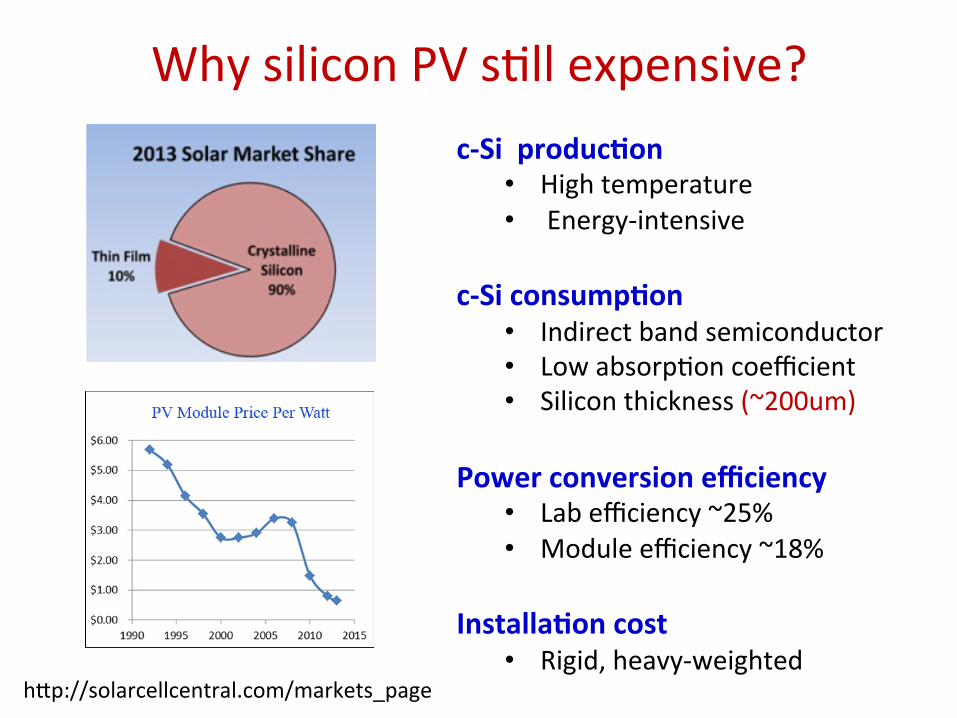
Why silicon PV s.ll expensive?
hBp://solarcellcentral.com/markets_page
c-‐Si produc+on • High temperature • Energy-‐intensive
c-‐Si consump+on • Indirect band semiconductor • Low absorp.on coefficient • Silicon thickness (~200um)
Power conversion efficiency • Lab efficiency ~25% • Module efficiency ~18%
Installa+on cost • Rigid, heavy-‐weighted
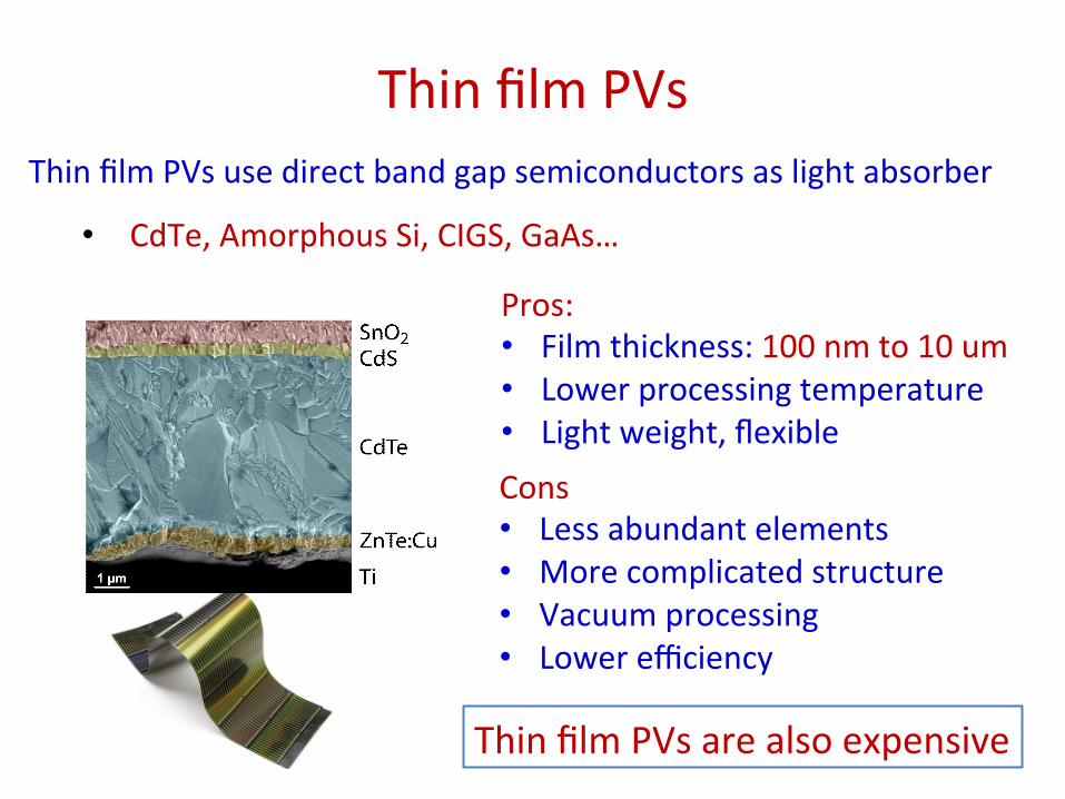
Thin film PVs Thin film PVs use direct band gap semiconductors as light absorber
• CdTe, Amorphous Si, CIGS, GaAs…
Cons • Less abundant elements • More complicated structure • Vacuum processing • Lower efficiency
Pros: • Film thickness: 100 nm to 10 um • Lower processing temperature • Light weight, flexible
Thin film PVs are also expensive

Mul.junc.on PV
D. Forbes and S.Hubbard, SPIE Newsroom, 26 July 2010,
High efficiency: 40% Extremely expensive

How to bring the PV cost down?
• Earth abundant elements
• Inexpensive fabrica.on § low-‐temperature § solu.on-‐ processing § roll-‐to-‐roll manufacturing
• High efficiency
• Easy installa.on § light weight § flexibility
Emerging PVs: • Dye sensi.zed solar cells (DSC) • Organic Solar cells
• Quantum dot solar cells
• CZTS solar cells • Perovskite solar cells (PSC)

h"p://www.nrel.gov/ncpv/
PSC

Organometal Halide Perovskites
CH3NH3PbI3
CH3NH3+ Pb2+ I-
A B X
Perovskite ABX3 (CaTiO3)
ü Low temperature
ü Solu.on processing ü Earth abundant elements
X
I-‐, cl-‐
CH3NH3PbI3-xClx
ü High absop.on ü Small exciton binding energy
ü Excellent charge mobili.es
J. Phys. Chem. Le"., 2013, 4(15), pp 2423-‐2429

Perovskite solar cells Mesoporous (DSC) vs Planar (thin film PV)
Snaith et al, Nature 501, 395-‐ 398 (2013). Snaith et al, Science 338, 643–647 (2012) Grätzel et al, Nature 499, 316-‐320 (2013)
Challenges: • Device structure • Hysteresis • “Lead” issue • Stability

Ø Perovskite light absorber: CH3NH3PbI3-‐xClx
Ø TiO2 :compact film, 20nm NPs, 200nm NPs
• Film deposi.on: one step spin coa.ng • ETM: TiO2 compact layer • HTM: Spiro-‐OMeTAD • Electrodes: Ag, FTO glass
Device fabrica.on
TiO2 compact film
200nm TiO2 NPs
20nm TiO2 NPs
500nm
VFP Research: The role of TiO2 Nanopa.cles
To examine the effect of TiO2 NPs on perovskite film morphology, crystal structure, op.cal and electronic proper.es, and device performance

User facili.es at CFN
Time-‐resolved Confocal Microscope
Hitachi s4800 SEM
Solar cell fabrica.on systems

Film morphology Compact TiO2
20nm NPs
200nm NPs
50um 5um 1um
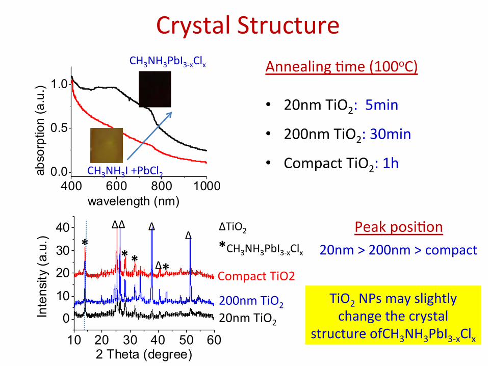
Crystal Structure
400 600 800 10000.0
0.5
1.0
abso
rptio
n (a
.u.)
wavelength (nm)
CH3NH3I +PbCl2
CH3NH3PbI3-‐xClx Annealing .me (100oC)
• 20nm TiO2: 5min
• 200nm TiO2: 30min
• Compact TiO2: 1h
Peak posi.on 20nm > 200nm > compact
10 20 30 40 50 60
0
10
20
30
40
Inte
nsity
(a.u
.)
2 Theta (degree)
* * * *
Δ Δ Δ
Δ
Δ
ΔTiO2
20nm TiO2 200nm TiO2
Compact TiO2
*CH3NH3PbI3-‐xClx
TiO2 NPs may slightly change the crystal
structure ofCH3NH3PbI3-‐xClx

PL of Perovskite films
20 40 60 8010-3
10-2
10-1
100
PS on glass PS on compact TiO2 film PS on 20nm TiO2 NPs PS on 200nm TiO2 NPs
PL
inte
nsity
(a.u
.)
Time (ns)
• Significant quenching of PL life.me indicates efficient electron
transfer
• Long life.me components in compact and 200nm TiO2 samples
• Varia.ons in spectra (peak posi.on and band width) suggest different
crystal/defects structures
700 8000.0
0.5
1.0
PL
inte
nsity
(a.u
.)
Wavelength (nm)
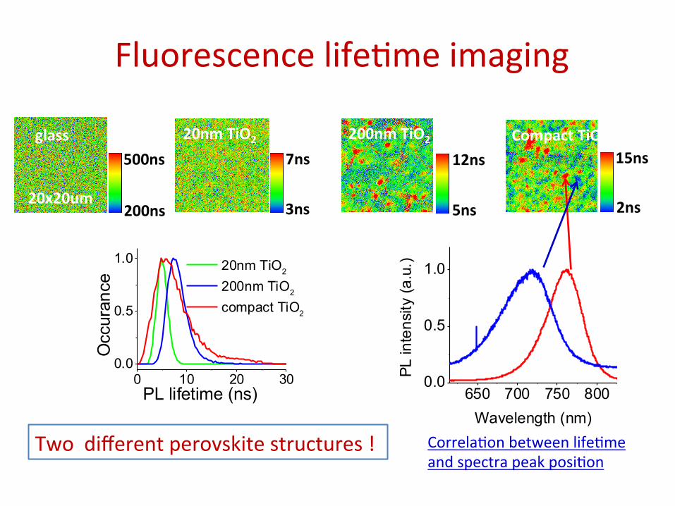
0 10 20 300.0
0.5
1.0 20nm TiO2 200nm TiO2
compact TiO2
Occ
uran
ce
PL lifetime (ns) 650 700 750 8000.0
0.5
1.0
PL in
tens
ity (a
.u.)
Wavelength (nm)
Fluorescence life.me imaging
200ns
500ns
3ns
7ns
5ns
12ns
2ns
15ns
20x20um
glass 20nm TiO2 200nm TiO2 Compact TiO2
Correla.on between life.me and spectra peak posi.on
Two different perovskite structures !

Acknowledgements
• DOE Visi.ng Faculty Program (VFP)
• Center for Func.onal Nanomateirals (CFN), BNL – Mircea Cotlet, Chang-‐Yong Nam, Gwen Wright, Mingzhao Liu, Huidong Zang, and many others
• Office of Educa.on Program (OEP), BNL – Neol Blackburn, Cindi Biancarosa, Sal Gonzalez, and the others