defect characterization, imaging, and control in wide
TRANSCRIPT

TOPICAL COLLECTION: 17TH CONFERENCE ON DEFECTS (DRIP XVII)
Defect Characterization, Imaging, and Control in Wide-BandgapSemiconductors and Devices
L.J. BRILLSON ,1,2,6 G.M. FOSTER,2 J. COX,1 W.T. RUANE,2
A.B. JARJOUR,2 H. GAO,2 H. VON WENCKSTERN,3 M. GRUNDMANN,3
B. WANG,4 D.C. LOOK,4 A. HYLAND,5 and M.W. ALLEN5
1.—Department of Electrical and Computer Engineering, The Ohio State University, Columbus,OH 43210, USA. 2.—Department of Physics, The Ohio State University, Columbus, OH 43210,USA. 3.—Institute for Experimental Physics, University of Leipzig, Postfach 10 09, 04103 Leipzig,Germany. 4.—Semiconductor Research Center, Wright State University, Dayton, OH 45435, USA.5.—Department of Electrical and Computer Engineering, University of Canterbury,Christchurch 8140, New Zealand. 6.—e-mail: [email protected]
Wide-bandgap semiconductors are now leading the way to new physical phe-nomena and device applications at nanoscale dimensions. The impact of de-fects on the electronic properties of these materials increases as their sizedecreases, motivating new techniques to characterize and begin to controlthese electronic states. Leading these advances have been the semiconductorsZnO, GaN, and related materials. This paper highlights the importance ofnative point defects in these semiconductors and describes how a complementof spatially localized surface science and spectroscopy techniques in threedimensions can characterize, image, and begin to control these electronicstates at the nanoscale. A combination of characterization techniquesincluding depth-resolved cathodoluminescence spectroscopy, surface photo-voltage spectroscopy, and hyperspectral imaging can describe the nature anddistribution of defects at interfaces at both bulk and nanoscale surfaces, theirmetal interfaces, and inside nanostructures themselves. These features aswell as temperature and mechanical strain inside wide-bandgap devicestructures at the nanoscale can be measured even while these devices areoperating. These advanced capabilities enable several new directions fordescribing defects at the nanoscale, showing how they contribute to devicedegradation, and guiding growth processes to control them.
Key words: Wide-bandgap semiconductor, defect, cathodoluminescencespectroscopy, surface photovoltage spectroscopy, hyperspectralimaging, ZnO, GaN, AlGaN, SiC, nanowire, high-electron-mobility transistor
INTRODUCTION
Wide-bandgap semiconductors are now at theforefront of solid-state electronics. These materialsare envisioned for a wide array of advanced elec-tronic structures such as: (1) transparent conduct-ing oxides (TCOs)1,2 for solar cells, biosensors, and
wearable electronics, (2) high-mobility two-dimen-sional electron gas (2DEG) heterojunctions3,4 forinterface superconductivity, magnetism, and multi-ferroicity, (3) high-frequency communication pack-ages with low dielectric loss for voltage-tunablefilters, oscillators, and phase shifters, and (4) low-leakage, high-breakdown-voltage structures for tun-nel junctions, high-k dielectric capacitors, and high-power transistors.5,6 Native point defects impactthese applications strongly by introducing recombi-nation and scattering centers that reduce mobility,(Received November 22, 2017; accepted March 7, 2018;
published online March 19, 2018)
Journal of ELECTRONIC MATERIALS, Vol. 47, No. 9, 2018
https://doi.org/10.1007/s11664-018-6214-9� 2018 The Minerals, Metals & Materials Society
4980

carrier and spin transport, optical emission, voltagecontrol, and device reliability.
Depth-resolved cathodoluminescence spec-troscopy (DRCLS)7 combined with surface photo-voltage spectroscopy (SPS),8 and hyperspectralimaging (HSI) can describe the nature and spatialdistribution of native point defects in bulk semicon-ductors, their microstructures, and their interfacesextending down to the nanoscale. With these opticaland electronic techniques, it is possible to charac-terize the impact of these defects on actual devicestructures, even while they are operating, in orderto gauge temperature and strain as well as how theycan introduce new defects that degrade deviceperformance. In turn, these characterization tech-niques can guide methods to reduce defects andimprove electronic properties.
EXPERIMENTAL PROCEDURES
The DRCLS technique9 involves an incident elec-tron beam that generates a cascade of secondaryelectrons. At keV energies, electrons lose energyfirst by generating x-rays, then plasmons, andfinally via impact ionization, which generates elec-tron-hole (e-h) pairs that can recombine across thesemiconductor bandgap or between band edges andstates within the bandgap.10 The intensities of thesegap-state features relative to the bulk band transi-tions provides a gauge of defect density which canbe calibrated using other techniques such as Hall-effect measurements, positron annihilation spec-troscopy (PAS), deep-level optical spectroscopy(DLOS), and transient surface photovoltage spec-troscopy (t-SPS). Use of scanning electron micro-scopy (SEM) provides nanoscale spatial resolutionboth depthwise and laterally. With HSI, i.e., single-wavelength intensity maps extracted from fullspectra acquired pixel by pixel across extendedareas,11 one can ‘‘map’’ the spatial distribution ofdefect luminescence laterally in two dimen-sions.12,13 Our DRCLS chambers’ ultrahigh-vacuum(UHV) environment enables electron beam energiesas low as 0.1 keV to provide near-nanometer depthresolution by avoiding nonradiative e-h recombina-tion due to surface carbon deposited from beam-dissociated CO2.
RESULTS AND DISCUSSION
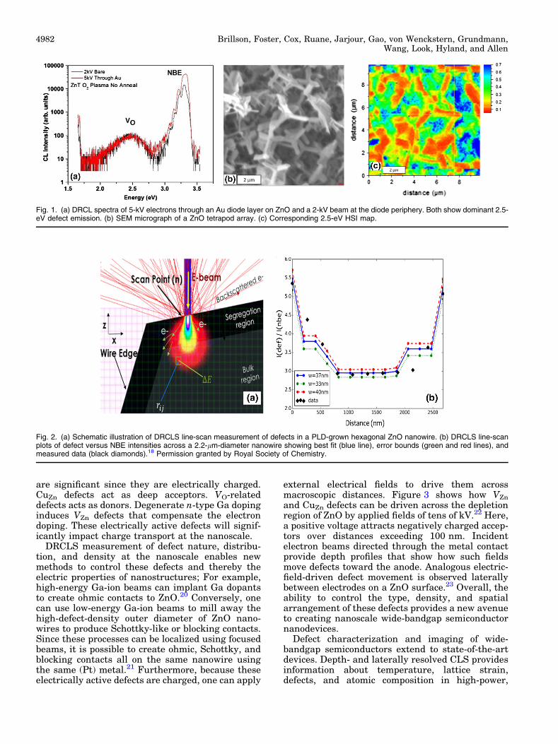
The lateral resolution of the DRCLS beam pro-vides useful information about Schottky barrierformation at metal interfaces with wide-bandgapsemiconductors; For example, Fig. 1a illustratesDRCL spectra taken from ZnO, both through anAu diode overlayer as well as at the bare ZnOperiphery.14 Spectral features include the near-band-edge (NBE) conduction-to-valence band emis-sion, longitudinal optical (LO) phonon replicasspaced at 73 meV multiples below the NBE peak,and a broad feature at 2.5 eV attributed to anoxygen-vacancy-related (VO-R) defect in the ZnO.
For more reactive metals such as Al or Ta, compar-ison of metallized versus bare surface spectrareveals metal-induced differences due to formationof near-interface defects.15 The depth resolution ofDRCLS enables one to probe the intimate metal-semiconductor interface, where diffusion and chem-ical reaction can produce defects.
The lateral resolution of DRCLS permits mea-surements of electronic inhomogeneity within indi-vidual metal diodes; For example, Ni diodes on 4H-SiC exhibit pronounced differences in deep-leveldefect emissions within the same 500-lm-diameterdiode.16,17 This diode exhibited two deep-level defectemissions, one which varied laterally inside thediode. As with similar diodes on the same surface,current-voltage (I-V) measurements exhibited ‘‘dou-ble-diode’’ behavior with kinks that exhibited twodistinct Schottky barrier heights. The Fermi levelEF positions within the SiC bandgap correspondingto these Schottky barriers corresponded closely tothe optical transition energies between the energylevels of the observed defects and the valence band.These results demonstrated that the deep-leveldefects observed at the nanoscale produced EF
‘‘pinning’’ that determined the macroscopic Schot-tky barrier I-V characteristics, regardless of themetal overlayer’s properties.
Native point defects can not only be localizedlaterally and at interfaces of wide-bandgap semi-conductors, but they may also distribute in threedimensions inside nanostructures. Figure 1b illus-trates an array of 300-nm- to 500-nm-diameter ZnOnanotripods. Figure 1c shows the HSI map of 2.5-eVVO-related defects inside individual ZnO nanowires.There is a high VO-R intensity at the free surfaces ofthe nanowires and a gradual decrease in defectintensity from surface to bulk over a thicknessrange of 50 nm to 100 nm. These images show thatnative point defects are inside as well as on thesurface of nanostructures.
Three-dimensional modeling of the DRCLS pro-cess can take into account the spatial distribution ofthe electron cascade’s energy loss, the distributionof defects, and the refraction of cathodolumines-cence emitted from inside the nanostructure.18
Figure 2a illustrates schematically the electroncascade positioned with respect to a specific distri-bution of defects inside a ZnO nanowire. Figure 2bshows defect intensities versus position in a profilemeasured transverse to the nanowire length, com-pared with trial defect distributions. These showthat VO-related defects extend hundreds of nanome-ters away from a free ZnO surface. Other ZnO nano-and microwires display different native pointdefects that depend on the method of growth.19
Thus, pulsed laser deposition (PLD) can exhibitfeatures due to CuZn substitutional impurities, dueto Cu impurities in the Zn source material. Chem-ical vapor deposition (CVD) can yield VO-R featuresas in Fig. 1a, whereas degenerately Ga-doped ZnOexhibits Zn vacancies VZn. These defect differences
Defect Characterization, Imaging, and Control in Wide-Bandgap Semiconductors and Devices 4981
are significant since they are electrically charged.CuZn defects act as deep acceptors. VO-relateddefects acts as donors. Degenerate n-type Ga dopinginduces VZn defects that compensate the electrondoping. These electrically active defects will signif-icantly impact charge transport at the nanoscale.
DRCLS measurement of defect nature, distribu-tion, and density at the nanoscale enables newmethods to control these defects and thereby theelectric properties of nanostructures; For example,high-energy Ga-ion beams can implant Ga dopantsto create ohmic contacts to ZnO.20 Conversely, onecan use low-energy Ga-ion beams to mill away thehigh-defect-density outer diameter of ZnO nano-wires to produce Schottky-like or blocking contacts.Since these processes can be localized using focusedbeams, it is possible to create ohmic, Schottky, andblocking contacts all on the same nanowire usingthe same (Pt) metal.21 Furthermore, because theseelectrically active defects are charged, one can apply
external electrical fields to drive them acrossmacroscopic distances. Figure 3 shows how VZn
and CuZn defects can be driven across the depletionregion of ZnO by applied fields of tens of kV.22 Here,a positive voltage attracts negatively charged accep-tors over distances exceeding 100 nm. Incidentelectron beams directed through the metal contactprovide depth profiles that show how such fieldsmove defects toward the anode. Analogous electric-field-driven defect movement is observed laterallybetween electrodes on a ZnO surface.23 Overall, theability to control the type, density, and spatialarrangement of these defects provides a new avenueto creating nanoscale wide-bandgap semiconductornanodevices.
Defect characterization and imaging of wide-bandgap semiconductors extend to state-of-the-artdevices. Depth- and laterally resolved CLS providesinformation about temperature, lattice strain,defects, and atomic composition in high-power,
Fig. 1. (a) DRCL spectra of 5-kV electrons through an Au diode layer on ZnO and a 2-kV beam at the diode periphery. Both show dominant 2.5-eV defect emission. (b) SEM micrograph of a ZnO tetrapod array. (c) Corresponding 2.5-eV HSI map.
Fig. 2. (a) Schematic illustration of DRCLS line-scan measurement of defects in a PLD-grown hexagonal ZnO nanowire. (b) DRCLS line-scanplots of defect versus NBE intensities across a 2.2-lm-diameter nanowire showing best fit (blue line), error bounds (green and red lines), andmeasured data (black diamonds).18 Permission granted by Royal Society of Chemistry.
Brillson, Foster, Cox, Ruane, Jarjour, Gao, von Wenckstern, Grundmann,Wang, Look, Hyland, and Allen
4982

high-frequency transistors. Figure 4a illustratesthe three-dimensional layer structure of anAlGaN/GaN high-electron-mobility transistor(HEMT), with arrows indicating the spatial rangeof DRCLS excitation both laterally and in depth. Ofparticular importance is the 2DEG layer (shown inred), the channel in which conduction takes place.Normal HEMT operation generates heat andmechanical strain due to the high voltages andcurrents involved. To measure local temperatures,one can monitor the NBE energy, which decreaseswith increasing temperature. The averaged depen-dence of energy versus temperature measuredexperimentally has a linear slope of�5.98 ± 0.12 9 10�4 eV/�C for GaN.24 Figure 4bshows a contour map of temperature measured ona line between gate and drain and extending fromthe surface past the 2DEG layer into the GaNlayers.25 Also displayed are the energies corre-sponding to depths of peak e-h excitation depth U0
obtained from a Monte Carlo simulation26 throughthe Si3N4 passivation surface layer of this HEMTstructure. As shown, the hottest spot in this effec-tive cross-sectional map under ON conditions is atthe drain-side gate edge, in agreement with devicemodeling simulations.27,28
Spatially localized measurements of mechanicalstrain are also useful to understand HEMT failureduring operation. A key indicator of device degra-dation is current leakage between gate and drainIDG with negative bias gate voltage. These OFFconditions induce mechanical strain between gateand 2DEG channel that is highest at the drain-sidegate foot. As with temperature, strain also producesNBE shifts, here shifting to higher energy by26 meV/GPa.29,30 With increasing drain-gate volt-age VDG, IDG rises sharply above a 28 V thresholdvoltage after an OFF-state, electric field-inducedstress. At this voltage, the NBE shifts by 7 meV,corresponding to an increase in stress of 0.27 GPa.Added to the lattice-mismatch stress alreadyinduced in the AlGaN layer by the underlyingGaN, this increase could exceed the mechanicalstrength of the crystal lattice due to an inversepiezoelectric effect.31,32
DRCLS coupled to Kelvin probe force microscopy(KPFM) measurements of electric potential acrosssurfaces provides imaging correlations betweennative point defects measured optically and elec-tronically. KPFM measures electric potential differ-ences between a scanning atomic force microscopy(AFM) tip and the bare AlGaN HEMT surface,providing two-dimensional maps of surface workfunction after device operation. KPFM maps ofsource-gate-drain regions with increasingly nega-tive VDG (OFF conditions) reveals the appearance oflow-potential regions at similar threshold voltages,regions that expand with increasing applied stress.Indeed, transistor failure occurs at regions with themost negative potential areas. Figure 5a illustratesan SEM secondary-electron image of a drain-gate-source region with a crater at the transistor’s failure
Fig. 3. DRCLS intensity ratio of VZn and CuZn peaks in ZnO versusNBE intensity with and without an 18.3 kV/cm positive bias appliedacross a 0.5-mm ZnO crystal.22 Reprinted with AIP permission.
Fig. 4. (a) Three-dimensional layer structure of AlGaN/GaN HEMT. Arrows show lateral and depth positions of DRCLS excitation. (b) Contourmaps of temperature in HEMT cross-section, showing elevated temperatures at drain-side gate edge and localized regions below. Inset showsexpanded dashed region with 2DEG.25 Reprinted with IEEE permission.
Defect Characterization, Imaging, and Control in Wide-Bandgap Semiconductors and Devices 4983

point.33 Figure 5b illustrates the correspondingKPFM potential maps of the extrinsic drain andsource regions to either side of a CL map of NBEemission intensity. Dashed circles indicateincreased potential regions that align with regionsof lower NBE emission. In turn, CL spectra of theseregions display increased characteristic 2.3-eV ‘‘yel-low band’’ (YB) and 2.8-eV ‘‘blue band’’ (BB) defectemission.34,35 Indeed, surface potential exhibits alinear dependence on NBE-normalized YB and BBintensities, decreasing as defect emission intensitiesincrease. Hence, both surface potential and CLmeasurements can map the defects. This correlation
is consistent with increased acceptor densities inthe AlGaN layer introducing a negative dipole thatlowers the measured surface EF.24
The energies of all these features are in goodagreement with GaN defect energies measured bydeep-level optical spectroscopy (DLOS)36–44 showinga dominant DLOS trap at EC—0.55 eV with trapdensity of 1012 cm�2. The bandgap complement ofthis energy level at 2.85 eV is consistent with the2.8-eV BB emission. Likewise, the bandgap comple-ment of a 1.1-eV DLOS-measured trap is 2.3 eV, inagreement with the 2.3-eV luminescence. DRCLspectra exhibit additional peak features correspond-ing to AlGaN defects and their NBE. SPS comple-ments CLS measurements by identifying theposition of the deep-level defects in the semiconduc-tor bandgap with respect to the band edges. Onsetsof photostimulated carrier population or depopula-tion result in potential changes that identify respec-tively the valence band (EV) or conduction band (EC)nature of the optical transition. SPS of the AlGaNsurface yields energy thresholds corresponding toAlGaN trap levels of EC—0.6 eV, 1.35 eV, 1.7 eV,and 2.0 eV, all in agreement with DLOS results.DRCL spectra as a function of depth for theEC—2.0 eV YB peak, the EC—1.35 eV BB peak,and a 3.75-eV feature (EC—0.6 eV bandgap comple-ment) map defect distributions below the HEMTsurface. Figure 6 illustrates the measurement ofthese NBE-normalized peak intensities from thedashed region indicated in the HEMT layer dia-gram. These depth profiles show that YB densitiesdecrease steadily from the outermost AlxGa1�xNsurface passivation layer, through the 50-nmAlGaN strain layer, and into the GaN substrate.In contrast, both the BB and the 3.75-eV defectsexhibit peak intensities inside the AlGaN layer.Thus, DRCLS depth profiles are able to map out thevarious depth dependences of HEMT defects on ascale of tens of nanometers or less and identifyspecific defects with specific layers.
Fig. 5. (a) SEM secondary-electron image of AlGaN/GaN HEMTgate region showing crater formed after device failure. (b) CL map ofNBE emission (middle) and KPFM map of potential (side). Dashedlines delineate extrinsic drain and source areas. Both red and blackcircles show similar higher defect and higher potential regions for CLand KPFM maps.33 Reprinted with AIP permission.
Fig. 6. AlGaN/GaN HEMT structure with dashed rectangle indicating region near the drain-side gate edge where yellow band (YB), blue band(BB), and 3.75-eV AlGaN deep-level defect densities are measured versus depth.
Brillson, Foster, Cox, Ruane, Jarjour, Gao, von Wenckstern, Grundmann,Wang, Look, Hyland, and Allen
4984

CONCLUSIONS
The results presented herein show that spatiallyresolved DRCLS can characterize, image, and insome cases, enable control of native point defects atwide-bandgap semiconductor interfaces and nanos-tructures in three dimensions and on a nanometerscale. CLS hyperspectral imaging reveals nativepoint defects inside wide-bandgap nano- and micro-wires. The physical nature and spatial distributionof these defects can vary strongly with their methodof growth. DRCLS can also measure the movementof defects under applied electric fields and theirreduction by removing material in which DRCLSmeasures their segregation. Three-dimensionalmapping of wide-bandgap devices can measuretemperature and stress at localized regions thatcontribute to device degradation and failure. Theability to separate electric-field-induced straineffects from current-induced heating establishestheir relative importance and underscores theimportance of inverse piezoelectric effects for HEMTdegradation. The capability to characterize andimage defects can be extended to many othermaterial systems, including 2D materials and inter-faces, complex oxide heterojunctions, and nanoscalebattery interfaces. Understanding the nature anddistribution of defects in these systems may providenew avenues for their control.
ACKNOWLEDGEMENTS
L.J.B., G.M.F., W.T.R., J.C., and H.G. gratefullyacknowledge National Science Foundation GrantNo. DMR-1305195. L.J.B. acknowledges Office ofNaval Research DRIFT MURI under GrantN00014-08-1-0655. H.v.W. and M.G. acknowledgeDeutsche Forschungsgemeinschaft for support withSonderforschungsbereich 762, ‘‘Functionality ofoxide interfaces’’ and GR 1011/23-1.
REFERENCES
1. S.C. Dixon, D.O. Scanlon, C.J. Carmalt, and I.P. Parkin, J.Mater. Chem. C 4, 6946 (2016).
2. K. Ellmer, Nat. Photonics 6, 809 (2012).3. H.Y. Hwang, Y. Iwasa, M. Kawasaki, B. Keimer, N. Na-
gaosa, and Y. Tokura, Nat. Mater. 11, 103 (2012).4. D.P. Kumah, A.S. Disa, J.H. Ngai, H. Chen, A. Malashe-
vich, J.W. Reiner, S. Ismail-Beigi, F.J. Walker, and C.H.Ahn, Adv. Mater. 26, 1936 (2014).
5. R.S. Pengelly, S.M. Wood, J.W. Milligan, S.T. Sheppard,and W.L. Pribble, IEEE Trans. Microw. Theory Technol.60, 1764 (2012).
6. G. Meneghesso, G. Verzellesi, F. Danesin, F. Rampazzo, F.Zanon, A. Tazzoli, M. Meneghini, and E. Zanoni, IEEETrans. Dev. Mater. Reliab. 8, 332 (2008).
7. L.J. Brillson, J. Phys. D Appl. Phys. 45, 183001 (2012).8. L. Kronik and Y. Shapira, Surf. Sci. Rep. 37, 1 (1999).9. A. Rose, RCA Rev. 27, 600 (1966).
10. B.G. Yacobi and D.B. Holt, Cathodoluminescence Micro-scopy of Inorganic Solids (New York: Plenum, 1990).
11. J. Christen, M. Grundmann, and D. Bimberg, J. Vac. Sci.Technol. B 9, 2358 (1991).
12. A. Gustafsson, M.-E. Pistol, L. Montelius, and L. Samuel-son, J. Appl. Phys. 84, 1715 (1998).
13. K. Thonke, I. Tischer, M. Hocker, M. Schirra, K. Fujan, M.Wiedenmann, R. Schneidter, M. Frey, and M. Feneberg,IOP Conf. Ser.: Mater. Sci. Eng. 55, 012018 (2014).
14. H.L. Mosbacker, S. El Hage, M. Gonzalez, S.A. Ringel, M.Hetzer, D.C. Look, G. Cantwell, J. Zhang, J.J. Song, andL.J. Brillson, J. Vac. Sci. Technol. B 25, 1405 (2007).
15. L.J. Brillson, H.L. Mosbacker, M.J. Hetzer, Y. Strzhe-mechny, G.H. Jessen, D.C. Look, G. Cantwell, J. Zhang,and J.J. Song, Appl. Phys. Lett. 90, 102116 (2007).
16. S. Tumakha, D.J. Ewing, L.M. Porter, Q. Wahab, X. Ma,T.S. Sudharshan, and L.J. Brillson, Appl. Phys. Lett. 87,242106 (2005).
17. D.J. Ewing, L.M. Porter, Q. Wahab, X. Ma, T.S. Sudhar-shan, S. Tumakha, M. Gao, and L.J. Brillson, J. Appl.Phys. 101, 114514 (2007).
18. W.T. Ruane, K.M. Johansen, K.D. Leedy, D.C. Look, H. vonWenckstern, M. Grundmann, G.C. Farlow, and L.J. Brill-son, Nanoscale 8, 7631 (2016).
19. L.J. Brillson, W.T. Ruane, H. Gao, Y. Zhang, J. Luo, H. vonWenckstern, and M. Grundmann, Mater. Sci. Semicond.Process. 57, 197 (2017).
20. J. He, J. Ke, P. Chang, K. Tsai, P. Yang, and I. Chan,Nanoscale 4, 3399 (2012).
21. A. Jarjour, J.W. Cox, W.T. Ruane, H. Von Wenckstern, M.Grundmann, and L.J. Brillson, Ann. der Physik, 530,1700335 (2018).
22. G.M. Foster, H. Gao, G. Mackessy, A.M. Hyland, M.W.Allen, B. Wang, D.C. Look, and L.J. Brillson, Appl. Phys.Lett. 111, 101604 (2017).
23. H. Gao, G.M. Foster, A.M. Hyland, M.W. Allen, and L.J.Brillson, unpublished.
24. A.P. Young and L.J. Brillson, Appl. Phys. Lett. 77, 699(2000).
25. C.-H. Lin, T.A. Merz, D.R. Doutt, J. Joh, J.A. del Alamo,U.K. Mishra, and L.J. Brillson, IEEE Trans. Electron De-vices 59, 2667 (2012).
26. D. Drouin, A. Real Couture, D. Joly, X. Tastet, V. Aimez,and R. Gauvin, Scanning 29, 92 (2007).
27. W.D. Hu, X.S. Chen, Z.J. Quan, C.S. Xia, W. Lu, and P.D.Ye, J. Appl. Phys. 100, 074501 (2006).
28. I. Ahmad, V. Kasisomayajula, M. Holtz, J.M. Berg, S.R.Kurtz, C.P. Tigges, A.A. Allerman, and A.G. Baca, Appl.Phys. Lett. 86, 173503 (2005).
29. C.H. Lin, D.R. Doutt, U.K. Mishra, T.A. Merz, and L.J.Brillson, Appl. Phys. Lett. 97, 223502 (2010).
30. K. Wan, A. Alan Porporati, G. Geng, H. Yang, and G.Pezzotti, Appl. Phys. Lett. 88, 251910 (2006).
31. J.A. del Alamo and J. Joh, Microelectron. Reliab. 49, 1200(2009).
32. J. Joh and J.A. del Alamo, Microelectron. Reliab. 50, 767(2010).
33. C.-H. Lin, T.A. Merz, D.R. Doutt, M.J. Hetzer, J. Joh, J.A.del Alamo, U.K. Mishra, and L.J. Brillson, Appl. Phys. Lett.95, 033510 (2009).
34. U. Kaufmann, M. Kunzer, H. Obloh, M. Maier, Ch. Manz,A. Ramakrishnan, and B. Santic, Phys. Rev. B 59, 5561(1999).
35. M.A. Reshchikov, D.O. Demchenko, A. Usikov, H. Helava,and Yu. Makarov, Phys. Rev. B 90, 235203 (2014).
36. S. Kamiya, M. Iwami, T. Tsuchiya, M. Kurouchi, J. Kika-wa, T. Yamada, A. Wakejima, H. Miyamoto, A. Suzuki, A.Hinoki, T. Araki, and Y. Nanishi, Appl. Phys. Lett. 90,213511 (2007).
37. M. Arakawa, S. Kishimoto, and T. Mizutani, Jpn. J. Appl.Phys. Part I 36, 1826 (1997).
38. A.R. Arehart, A.C. Malonis, C. Poblenz, Y. Pei, J.S. Speck,U.K. Mishra, and S.A. Ringel, Phys. Stat. Sol. C 8, 2242(2011).
39. A.R. Arehart, A.C. Malonis, C. Poblenz, Y. Pei, J.S. Speck,U.K. Mishra, and S.A. Ringel, IEEE IEDM, p. 20.1 (2010).
Defect Characterization, Imaging, and Control in Wide-Bandgap Semiconductors and Devices 4985

40. M. Tapajna, U.K. Mishra, and M. Kuball, Appl. Phys. Lett.97, 023503 (2010).
41. J. Joh and J.A. del Alamo, IEEE Trans. Electron Devices58, 132 (2011).
42. M. Meneghini, A. Stocco, M. Bertin, D. Marcon, A. Chini, G.Meneghesso,andE.Zanoni,Appl.Phys.Lett.100,033505(2012).
43. Y. Puzyrev, T. Roy, M. Beck, B.R. Tuttle, R.D. Schrimpf,D.M. Fleetwood, and S.T. Pantelides, J. Appl. Phys. 109,034501 (2011).
44. D.W. Cardwell, A. Sasikumar, A.R. Arehart, S.W. Kaun, J.Lu, S. Keller, J.S. Speck, U.K. Mishra, S.A. Ringel, and J.P.Pelz, Appl. Phys. Lett. 100, 193507 (2012).
Brillson, Foster, Cox, Ruane, Jarjour, Gao, von Wenckstern, Grundmann,Wang, Look, Hyland, and Allen
4986