decoupling capacitor design issues in 90nm cmos
TRANSCRIPT

DECOUPLING CAPACITOR DESIGN ISSUES IN 90NM CMOS
by
XIONGFEI MENG
B.A.Sc., The University of British Columbia, 2004
A THESIS SUBMITTED IN PARTIAL FULFILMENT OF THE REQUIREMENTS FOR THE DEGREE OF
MASTER OF APPLIED SCIENCE
in
THE FACULTY OF GRADUATE STUDIES
(Electrical and Computer Engineering)
The University of British Columbia
April 2006
© Xiongfei Meng, 2006

ABSTRACT
On-chip decoupling capacitors (decaps) are widely used to reduce power supply noise. Typically,
designs use NMOS decaps between standard-cell blocks and NMOS+PMOS decaps within the
blocks. Starting at the 90nm CMOS technology node, the traditional decap designs may no
longer be suitable due to increased concerns regarding thin-oxide gate leakage and electrostatic
discharge (ESD) reliability. This thesis investigates new decap design approaches that address
gate leakage and ESD. A cross-coupled design is described that has been recently introduced by
cell library developers to handle ESD problems. Three modifications of the cross-coupled design
are introduced here and the tradeoffs among transient response, gate leakage and ESD
performance are analyzed. The modifications offer designers greater flexibility in decoupling
capacitor design for 90nm and below. To improve the power-grid noise reduction capability in
the areas between blocks, two versions of a switched-decap design are proposed. One provides
excellent decap performance but consumes large power, whereas the other saves power but
suffers from excessive delay. A novel low-power voltage regulator using switched decaps is
proposed to better balance performance and power consumption.
ii

TABLE OF CONTENTS
ABSTRACT.................................................................................................................................. II
TABLE OF CONTENTS ...........................................................................................................III
LIST OF TABLES ....................................................................................................................... V
LIST OF FIGURES ....................................................................................................................VI
ACKNOWLEDGMENTS .......................................................................................................VIII
CHAPTER 1 INTRODUCTION.................................................................................................. 1
1.1 MOTIVATION ........................................................................................................................ 1
1.2 DECOUPLING CAPACITORS ISSUES AT 90NM ....................................................................... 5
1.3 RESEARCH OBJECTIVES ....................................................................................................... 7
1.4 ORGANIZATION OF THE THESIS ........................................................................................... 8
CHAPTER 2 BACKGROUND................................................................................................... 10
2.1 INTRODUCTION ................................................................................................................... 10
2.2 DECOUPLING CAPACITOR MODELING .............................................................................. 11
2.3 GATE TUNNELING LEAKAGE ............................................................................................. 12
2.4 ELECTROSTATIC DISCHARGE RELIABILITY IN DECAP DESIGN........................................ 15
2.5 STANDARD-CELL DECAP LAYOUT AND PLACEMENT........................................................ 17
CHAPTER 3 EXISTING DECOUPLING CAPACITOR DESIGN APPROACHES .......... 22
3.1 INTRODUCTION ................................................................................................................... 22
3.2 CROSS-COUPLED DECAP.................................................................................................... 22
3.3 GATED DECAP .................................................................................................................... 25
3.4 THICK OXIDE DECAP ......................................................................................................... 28
3.5 HIGH-K GATE DIELECTRIC................................................................................................ 30
3.6 METAL-INSULATOR-METAL CAPACITOR ......................................................................... 32
3.7 SUMMARY ........................................................................................................................... 33
CHAPTER 4 PASSIVE DECOUPLING CAPACITOR DESIGNS ....................................... 34
iii

4.1 INTRODUCTION ................................................................................................................... 34
4.2 RC MODELING OF BASIC CROSS-COUPLED DECAP DESIGN ............................................ 34
4.3 TRANSIENT RESPONSE SIMULATION ................................................................................. 36
4.4 ESD PERFORMANCE SIMULATION..................................................................................... 42
4.5 GATE LEAKAGE SIMULATION............................................................................................ 44
4.6 MODIFIED CROSS-COUPLED DECAP DESIGNS .................................................................. 45
CHAPTER 5 ACTIVE DECOUPLING CAPACITOR DESIGNS ........................................ 51
5.1 INTRODUCTION ................................................................................................................... 51
5.2 SWITCHED DECOUPLING CAPACITOR ............................................................................... 52
5.3 SUN’S VOLTAGE REGULATOR............................................................................................ 55
5.4 FUJITSU’S ACTIVE POWER STABILIZER ............................................................................ 59
5.5 LOW-POWER VOLTAGE REGULATOR................................................................................ 63
5.6 SIMULATION SETUP AND RESULTS .................................................................................... 67
CHAPTER 6 CONCLUSIONS AND FUTURE WORK ......................................................... 74
6.1 SUMMARY ........................................................................................................................... 74
6.2 CONTRIBUTIONS IN THIS THESIS........................................................................................ 76
6.3 FUTURE WORK ................................................................................................................... 76
REFERENCES............................................................................................................................ 78
iv

LIST OF TABLES
TABLE 4.1: COMPARISON ON ESD PERFORMANCE, TRANSIENT RESPONSE AND GATE LEAKAGE. ... 47
TABLE 5.1: NODE BIASING AND SWING FOR SUN VOLTAGE REGULATOR [41]................................. 56
TABLE 5.2: NODE BIASING AND SWING FOR FUJITSU ACTIVE POWER STABILIZER [42]. .................. 61
TABLE 5.3: NODE BIASING AND SWING FOR LOW-POWER VOLTAGE REGULATOR. .......................... 64
v

LIST OF FIGURES
FIGURE 1.1: TWO COMPONENTS OF POWER SUPPLY NOISE [3]. ......................................................... 2
FIGURE 1.2: USE OF DECOUPLING CAPACITOR TO REDUCE POWER GRID NOISE [3]. .......................... 4
FIGURE 1.3: DECOUPLING CAPACITOR IMPLEMENTED USING AN NMOS DEVICE. ............................ 5
FIGURE 2.1: DECAP MODELING AS A SERIES RC CIRCUIT................................................................ 11
FIGURE 2.2: GATE LEAKAGE CURRENT VERSUS GATE AREA. .......................................................... 13
FIGURE 2.3: GATE LEAKAGE CURRENT DENSITY VERSUS OXIDE THICKNESS. ................................. 14
FIGURE 2.4: COMPLETE ESD PROTECTION SCHEME. ...................................................................... 16
FIGURE 2.5: STANDARD CELL N+P DECAP CONFIGURATION. ......................................................... 17
FIGURE 2.6: SAMPLE LAYOUT OF STANDARD-CELL N+P DECAP WITH NO FINGERS. ....................... 18
FIGURE 2.7: SAMPLE LAYOUT OF STANDARD-CELL N+P DECAP WITH TWO FINGERS...................... 18
FIGURE 3.1: CROSS-COUPLED DECAP SCHEMATIC [11]................................................................... 23
FIGURE 3.2: INTUITIVE UNDERSTANDING OF INPUT RESISTANCE IN CROSS-COUPLED DESIGN......... 24
FIGURE 3.3: BASIC GATED DECAP SCHEMATIC [12] AND GATE LEAKAGE FLOW. ............................ 25
FIGURE 3.4: SAMPLE CLOCK FOR THE CTRL SIGNAL IN GATED DECAP. ........................................... 27
FIGURE 3.5: INSERTION OF SMALL INVERTER IN GATED DECAP [12]............................................... 27
FIGURE 3.6: STACK OF THIN-OXIDE DECAPS VERSUS THICK-OXIDE DECAP. .................................... 29
FIGURE 4.1: CROSS-COUPLED DECAP SCHEMATIC [11] AND MODELING. ........................................ 35
FIGURE 4.2: SCHEMATIC FOR THE FIRST TRANSIENT SETUP. ........................................................... 37
FIGURE 4.3: RC MODELING OF THE FIRST TRANSIENT SETUP. ......................................................... 37
FIGURE 4.4: SIMPLIFICATION OF RC MODELING OF THE FIRST TRANSIENT SETUP........................... 38
FIGURE 4.5: TRANSIENT RESPONSE FOR THE FIRST SETUP. ............................................................. 40
FIGURE 4.6: SCHEMATIC FOR THE SECOND TRANSIENT SETUP. ....................................................... 41
vi

FIGURE 4.7: TRANSIENT RESPONSE FOR THE SECOND SETUP. ......................................................... 42
FIGURE 4.8: SIMULATION SETUP FOR ESD ANALYSIS [10]. ............................................................ 43
FIGURE 4.9: SAMPLE LAYOUT OF MOD1 (BASIC CIRCUIT WITHOUT FINGERING)............................. 45
FIGURE 4.10: SAMPLE LAYOUT OF MOD2 (REPLACE NMOS WITH PMOS).................................... 46
FIGURE 4.11: SAMPLE LAYOUT OF MOD3 (REPLACE NMOS WITH PMOS, AND USE SMALLEST
NMOS).................................................................................................................................. 47
FIGURE 4.12: COMPLETE TRANSIENT RESPONSE FOR THE FIRST SETUP........................................... 48
FIGURE 4.13: COMPLETE TRANSIENT RESPONSE FOR THE SECOND SETUP....................................... 49
FIGURE 5.1: PRINCIPLE OF SWITCHED DECOUPLING CAPACITOR [40]. ............................................ 52
FIGURE 5.2: MOS IMPLEMENTED SWITCHED DECOUPLING CAPACITOR [40]-[42]. ......................... 54
FIGURE 5.3: BLOCK DIAGRAM OF SUN VOLTAGE REGULATOR [41]. ............................................... 55
FIGURE 5.4: CIRCUIT IMPLEMENTATION OF SUN VOLTAGE REGULATOR [40] [41].......................... 57
FIGURE 5.5: CIRCUIT IMPLEMENTATION OF FUJITSU ACTIVE POWER STABILIZER [42].................... 60
FIGURE 5.6: CIRCUIT IMPLEMENTATION OF LOW-POWER VOLTAGE REGULATOR............................ 65
FIGURE 5.7: SIMULATION SETUP FOR ACTIVE DECAP CIRCUITS....................................................... 69
FIGURE 5.8: SIMULATION RESULTS FOR NO DECAP INSERTED......................................................... 70
FIGURE 5.9: SIMULATION RESULTS FOR STANDARD DECAPS INSERTED. ......................................... 70
FIGURE 5.10: SIMULATION RESULTS FOR SUN VR INSERTED. ........................................................ 71
FIGURE 5.11: SIMULATION RESULTS FOR FUJITSU APS INSERTED. ................................................ 71
FIGURE 5.12: SIMULATION RESULTS FOR LOW-POWER VR INSERTED. ........................................... 72
vii

ACKNOWLEDGMENTS
I would like to express my gratitude to my academic supervisor, Dr. Resve Saleh, whose
expertise, understanding, patience, and support, added significantly to my graduate experience. I
appreciate his profound and vast knowledge in many areas, both within and outside of the scope
of my research. I would like to thank my industrial supervisor, Dr. Karim Arabi, for his technical
advice, encouragement, and kindness.
A very special thanks to my colleagues and friends in the SoC group, without whose assistance, I
would not have accomplished this research. More specifically, I would like to thank Amit Kedia,
Dipanjan Sengupta, Karim Allidina, Reza Molavi, Scott Chin, Roberto Rosales, Roozbeh
Mehribadi, and Dr. Steve Wilton. I also thank Dr. Shahriar Mirabbasi who provided me with
technical and personal support whenever I asked and became more of a mentor and friend, than a
professor. I also acknowledge Asad Shayan and Mamta Bansal of PMC-Sierra Inc. for their
suggestions and help in this study.
I recognize that this research would not have been possible without the financial support from
NSERC and PMC-Sierra Inc., and express my gratitude to them. I also thank CMC
Microsystems for providing the CAD tools.
Last, but not least, I would especially like to thank my family for both giving and encouraging
me to seek for myself a demanding and meaningful education. In particular, I must acknowledge
my fiancée, Liming, for her love, caring and patience through many years of my life. The
appreciation extends beyond any words at my command.
viii
Chapter 1
Introduction
1.1 Motivation
As integrated circuit (IC) technology scales, more and more transistors are being placed within a
single chip, while the clock frequency continues to increase into the gigahertz range. The result
is that large transient currents are drawn from the power supply rails in just a few hundred
picoseconds [1] in modern custom and application-specific integrated circuit (ASIC) chips.
Meanwhile, the supply voltage is scaled with technology to reduce overall power consumption,
and as a consequence, the circuitry becomes more prone to power-supply noise. The
management and regulation of the quality of the on-chip power supply is a major challenge [1].
The power grid, which provides VDD and VSS (or ground) signals throughout the chip,
experiences fluctuations in value due to a variety of noise sources. If the supply voltage noise or
variation is excessively large, it may lead to problems such as delay variation, timing
unpredictability, or even improper functionality [2]. A commonly used metric, noise budget, is
defined as the maximum allowable noise amplitude [3]. Typically, it is required to keep the
power supply noise within a certain percentage (e.g., 10%) of the nominal supply voltage VDD.
1

Namely, 10% of VDD – VSS is typically the noise budget, a rule-of-thumb used in the industry [4].
Circuit designers must ensure that the chip operates correctly if the maximum voltage difference
between VDD and VSS is 10% or smaller than the nominal value.
In today’s advanced deep-submicron (DSM) technology, the power grid noise is due to two main
issues: (1) As the power lines made of metal wires become thinner, the wire resistance R
increases. When logic gates switch and a current I flow through the power lines to deliver charge
to the gates, the voltage drop ΔV at the gates is ΔV1 = I R⋅ . This type of power-supply noise is
known as IR drop. (2) Due to package pin inductance and thin-interconnect inductance, the
power lines experience inductance effect when the current flow changes with respect to time.
This second source of voltage drop is given by ΔV2 = dILdt
. The two power supply noise
components are illustrated in Figure 1.1, which depicts two inverters connected to an off-chip
voltage supply through the on-chip power grid.
Figure 1.1: Two components of power supply noise [3].
Considering the two components together, the overall voltage drop ΔV at any point in the power
grid is:
2

dIV IR Ldt
Δ = + (1.1)
To illustrate the IR drop, all the nodes in the power grid are initially charged to VDD with no
activity in the circuit. As the second inverter starts to switch, the wire resistance along the VDD
line creates voltage drops as current flows from the external voltage source towards the second
inverter [3]. Similarly, the ground grid is subject to the same type of problem when the outputs
of the buffers switch low, except that the voltage level of the ground line will increase. This is
sometimes referred to as ground bounce. In practice, IR drop can be caused by simultaneous
switching of clock buffers, bus drivers, memory decoder drivers, and so on, when there is high
activity in the circuit. These simultaneous switching activities can happen anywhere on the chip.
Thus, all regions in the chip are susceptible to IR drop. In a wire-bond (e.g., dual-inline) package,
the supply voltage level remains relatively high at the periphery of chip where the voltage supply
I/O pads are located, and drops noticeably at the centre of the chip. In contrast, in a flip-chip (or
ball-grid array) package, the centre of the die has rather high voltage level, whereas the periphery
of the die experiences larger IR drops.
Considering the Ldi/dt term in Equation (1.1), the inductance L is another source of voltage drop
in the power supply and is typically at 1 to 2 nH in a dual-inline package (DIP) or at roughly 0.1-
0.2nH in a ball-grid array (BGA) package [3]. In a traditional DIP package, this inductance arises
from the bonding wire used to connect the chip I/O pads to the lead pins. On the other hand, in a
modern ceramic BGA package, the inductance comes from the solder bumps that can be placed
anywhere in the chip area [5]. Although BGA is a more expensive solution, it provides more I/O
connection capability and less inductance value [3].
3

In the past, compared to IR drop, the Ldi/dt term was not considered as a significant source of
power supply noise, mainly because the chip clocks were not running at the gigahertz range.
However, in today’s chips, this inductance effect is a much more significant [6]. The value of L
has not changed considerably over the years, while the value of di/dt has continued to increase
due to faster and faster clock frequencies.
A common technique for reducing power supply noise and keeping the noise within the noise
budget is through the use of on-chip decoupling capacitors (decaps). Decaps are essentially
capacitors that hold a reservoir of charge and are placed close to the power pads and near any
large drivers. When large drivers switch, the decaps provide instantaneous current to the drivers
to reduce IR drop and Ldi/dt effects, and hence keep the supply voltage relatively constant. As
shown in Figure 1.2, the on-chip decap delivers current to charge up the load capacitance of the
second inverter when it switches. The supply voltage level is relatively constant at the inverter
tap point since the decap is nearby, so ΔV is minimal.
Figure 1.2: Use of decoupling capacitor to reduce power grid noise [3].
This thesis focuses on the issues of power supply noise reduction through the use of decoupling
capacitors. In a typical ASIC design, decaps can be placed in the open areas of the chip between
4

intellectual property (IP) blocks (called white-space decaps, or global decaps) and within the IP
blocks composed of standard cells [7]. The thesis discusses both types of on-chip decaps,
although off-chip decaps are commonly used as well [8].
1.2 Decoupling Capacitors Issues at 90nm
A standard decap is usually made from NMOS transistors in a CMOS process [3]. As shown in
Figure 1.3, the gate of the NMOS transistor is connected to VDD, whereas source, drain and
substrate of the transistor are tied to VSS. This approach is considered effective because the thin-
oxide capacitance of the transistor gate provides a higher capacitance than any other oxide
capacitance available in a standard CMOS fabrication process [4]. For this MOS decap, the first-
order calculation of the capacitance is WLCOX, where W is the transistor width, L is the transistor
length, and COX is the oxide capacitance per unit area. Accurate capacitance model needs to
include the parasitic fringing and overlap capacitance of the transistor, and will be discussed in
greater detail in Chapter 2.
Figure 1.3: Decoupling capacitor implemented using an NMOS device.
At the 90nm technology node, the oxide thickness of a transistor is reduced to roughly 2.0nm or
less. The thin oxide causes two new problems: possible electrostatic discharge (ESD) induced
oxide breakdown and gate tunneling leakage [9], [10]. Potential ESD oxide breakdown increases
5
the likelihood that an IC will be permanently damaged during an ESD event, and hence raises a
reliability concern. Higher gate tunneling leakage increases the total static power consumption of
the chip. As technology scales further down, with a thinner oxide, the result is an even higher
ESD risk and more gate leakage. The standard decap design using NMOS transistors experiences
these two problems and therefore becomes rather inappropriate for 90nm and below.
While satisfying ESD reliability and gate leakage limitations, decap designs must also meet the
transient performance requirements. Since a 90nm process (or below) usually provides the
capability of running at gigahertz frequencies, the decap must respond in the order of a hundred
picoseconds.
A new cross-coupled standard-cell design approach [11] addresses the issue of ESD performance.
The design provides a certain amount of ESD input protection to the decap, but does not offer
any savings in gate leakage. Even worse, the new design experiences a much degraded transient
response, making it somewhat unsuitable for high-speed chips. Modifications to the cross-
coupled decap design that properly trades off ESD, transient response and gate leakage are
needed.
Another new global decap design approach, called gated decap, has been reported [12] to control
gate leakage. Based on the approach of multi-threshold CMOS circuit, the gated decap is capable
of saving a significant amount of leakage current while in power-saving mode. However, the
design suffers from an oscillation problem. The lack of robustness of the design makes it
somewhat less attractive for industrial use.
6

Most fabrication processes provide high-voltage thick-oxide I/O transistors. Those transistors
have properties of excellent ESD reliability and almost-zero gate leakage. These desired
properties make them good candidates for global decap implementation in 90nm or below.
However, the effective capacitance for such thick-oxide decaps is much less than thin-oxide ones.
Certain fabrication limitations also apply for thick-oxide devices.
From a process perspective, the use of high-k gate dielectrics is an active field. Progress has been
made to provide savings in gate leakage. Nevertheless, many process issues still exist and the
high-k technology is far from mature enough for mass production. Metal-insulator-metal
capacitors are available in many fabrication processes. It is useful to examine if those capacitors
are suitable for making global decaps since it is known that the leakage current for such a
capacitor is low.
For global decaps, to improve the area efficiency, the use of switched decoupling capacitors is an
interesting alternative. Compared to the passive designs, the intent of the switched decaps is to
boost the supply voltage to provide better power-grid noise reduction capability. Two existing
designs from Sun and Fujitsu are worth investigating, and improving for low-power operation.
Such a low-power voltage regulator would be suitable for general low-power applications in both
ASIC and custom designs.
1.3 Research Objectives
The research objectives of this work are as follows:
7

• Understand relationship between critical decap design issues, such as electrostatic
discharge reliability, gate leakage and transient response.
• Develop passive solutions to decap designs that properly trade off gate leakage, ESD and
transient response, and provide designers with design flexibility for sub-90nm
technologies for standard-cell decaps.
• Explore active solutions to decap designs that provide better power-grid noise reduction
capability than the passive approaches. Design a novel switched-decap voltage regulator
that properly balances power dissipation and decap performance in white-space decaps.
1.4 Organization of the Thesis
The remainder of this thesis is organized as follows. Chapter 2 provides the necessary
background for decap modeling, gate tunneling leakage phenomenon, ESD reliability, and
standard-cell placement of decoupling capacitors.
Chapter 3 explores various decap design approaches that may be suitable for upcoming
technologies. The circuit-level designs are discussed first, followed by the process-level efforts.
The pros and cons of each approach are provided.
Chapter 4 develops a set of new designs based on the cross-coupled decap. The modeling of the
new designs is described to allow hand calculations and analyses to be carried out. The new
designs are validated using a full set of simulations in transient, ESD and gate leakage
measurements. Based on the simulation results, the proper layout of these designs is described.
Chapter 5 analyzes the advantages and disadvantages of Sun’s voltage regulator and Fujitsu’s
active power stabilizer to improve decap area efficiency. A novel low-power switched-decap
8

voltage regulator is designed to achieve good power-grid noise reduction performance while
maintaining a low level of dc power consumption.
Chapter 6 summarizes the results of the thesis and provides conclusions. Future research
directions are provided.
9

Chapter 2
Background
2.1 Introduction
The topics in this chapter provide the necessary background for the rest of the thesis. Moreover,
some fundamental and practical decap design issues are highlighted in this chapter to motivate
the topics in the remainder of the thesis. This chapter begins with modeling of standard NMOS
decaps. An overview of design challenges and problems associated with decoupling capacitors in
90nm and below is provided. The overview includes gate tunneling leakage, electrostatic
discharge phenomenon and protection, and standard-cell decap placement. The gate leakage is
introduced from a physical point of view, and useful information from recent technologies is
given. ESD reliability is presented and typical phenomena during an ESD event are discussed.
Primary and local ESD protection schemes are briefly illustrated. Since ASIC designs typically
utilize standard cells, the decap insertion and placement procedure within standard-cell blocks is
briefly introduced.
10

2.2 Decoupling Capacitor Modeling
A standard decap is usually implemented using an NMOS transistor with the gate connected to
VDD and both source and drain connected to VSS, or a PMOS device with opposite connections.
When implemented using MOS transistors, decaps experience parasitic channel resistance that
imposes certain delay on the transient response of the decap [4] [13]. Therefore, a decap should
be modeled as a series connection of effective resistance and effective capacitance [4], as shown
in Figure 2.1.
Figure 2.1: Decap modeling as a series RC circuit.
For precise calculation, the effective capacitance at low frequencies can be written as:
(2.1) 2eff OX OLC C WL C W= +
where COX is the oxide capacitance per unit area, COL is the overlap and fringing capacitance per
unit width, and W and L are the width and length of the transistor, respectively.
The decap’s effective resistance at low frequencies is given by [4]:
6 (eff
OX GS T
LRC W V Vμ
=− )
(2.2)
where μ is the channel mobility, VGS (or VGD since source and drain are tied) is the voltage
across the oxide, and VT is the threshold voltage. From Equation (2.2), Reff is proportional to the
11
channel length L. That is, for faster transient response, a decap design should use a small L to
keep Reff small. Both Reff and Ceff can be considered constant at low or moderate operating
frequencies, but they are degraded a high frequencies [4] [14].
Since decaps are usually built using MOS transistors, the high-frequency behavior of MOS
transistors needs to be investigated. Previous work in [4] has shown that both Reff and Ceff will
decay as operating frequency increases. That is, both Reff and Ceff are functions of frequency, f.
Although it is desired to have a small Reff, the decreased Ceff results in reduced capability of the
decap at high frequencies.
The channel length L of the decap controls its frequency response. If L is small enough, the
effective capacitance remains relatively constant at high frequencies. As a consequence, a
fingering technique in decap layout is commonly used to maintain its frequency response [4].
Moreover, NMOS has better frequency response than PMOS [4]. Thus, the use of PMOS decaps
should be limited, from the frequency response perspective.
2.3 Gate Tunneling Leakage
A new design issue for decaps due to oxide thickness reduction is the gate tunneling current. The
current is in the form of tunneling electrons or holes from substrate to gate or from gate to
substrate through the gate oxide, depending on the voltage biasing conditions [15]. Two forms of
gate tunneling exist: Fowler–Nordheim (FN) tunneling and direct tunneling. For normal
operations on short-channel devices, FN tunneling is negligible, and direct tunneling is dominant
[15]. In the case of direct tunneling, the gate leakage current in PMOS is much less than in
12

NMOS, and it has been shown experimentally that PMOS gate leakage is roughly 3 times
smaller than NMOS gate leakage for same size transistors [16] [17]. The gate leakage
simulations can be carried out by using BSIM4 SPICE models [18] [19]. Assuming a 90nm
technology with 2.0nm oxide thickness and 1.0V power supply, the gate leakage current is
shown in Figure 2.2.
Figure 2.2: Gate leakage current versus gate area.
The gate leakage current density J and the oxide thickness tOX have an empirical relationship as
follows, assuming the voltage across the oxide VOX is fixed [16]:
(2.3) (10 OXA B tJ − ⋅= )
where A and B are experimental constants and are process dependent. Equation (2.3) implies that
the gate leakage current is exponentially related to the oxide thickness. A typical J and tOX
relationship for a fixed VOX is illustrated in Figure 2.3.
13

Figure 2.3: Gate leakage current density versus oxide thickness.
It is evident that from 90nm technology onward, the gate leakage from decaps will be significant
[17]. The gate leakage contributes to the total static power consumption, and decaps usually
occupy a large on-chip area. The use of PMOS devices exclusively is not a viable solution for
high-frequency circuits since they have a poor frequency response relative to the NMOS devices
[4].
In addition, the amount of gate leakage is also a strong function of the applied bias [20]. If the
transistor has a VOX that is roughly equal to VDD, the leakage current density is largest. If the
transistor has a VOX set to close or below VT, it leaks significantly less. Indeed, under such a
condition, the gate leakage current is typically 3-6 orders of magnitude less, depending on the
values of VDD and tOX [20]. Thus, the gate leakage in the second condition can be roughly
considered to be zero. In decaps, the gate is at VDD and the source and drain of a transistor are
tied together. Therefore, decaps would experience the highest levels of leakage.
14

2.4 Electrostatic Discharge Reliability in Decap Design
Another new consideration has arisen in the form of ESD protection due to the thin oxide in
90nm technology. ESD is the process of static discharge that can typically arise from human
contact with any IC pin. Approximately 0.6uC of charge is carried on a body capacitance of
100pF, generating a potential of 2kV or higher to discharge from the contacted IC pin to ground
for a duration of more than 100ns [10]. Under such an event, the peak discharge current is in the
ampere range, leading to permanent damage on certain transistors in the chip if not properly
protected. The damage can be in one of two forms, or a combination of the two: one is thermal
burnout in devices or interconnects, while the other is oxide breakdown of devices due to the
high voltage across the oxide [10]. When running simulations for an ESD event, the maximum
current density Jmax of devices and interconnects is measured to check for potential thermal
damage. The oxide voltage also needs to be measured to compare with the oxide breakdown
voltage of a device for a given fabrication process. The oxide breakdown voltage is almost
linearly proportional to the oxide thickness [10]. For instance, assuming a 90nm process uses
2.0nm of oxide thickness, the corresponding oxide breakdown voltage is just below 5V. If the
thickness is doubled, the oxide breakdown voltage is also doubled to around 10V [10].
An ESD event can be delivered between any two pins of an IC. To properly protect an IC from
ESD damage, an ESD circuit must shunt ESD current between these two pins [10]. In the case of
decaps within standard cells, the only two pins that the decaps have access to are the two local
power rails, namely VDD and VSS. Primary and local (sometimes called secondary) protection
elements are needed to protect the two rails by limiting the voltage difference between the two
rails to a value below the oxide breakdown voltage. The primary element will shunt most of the
15
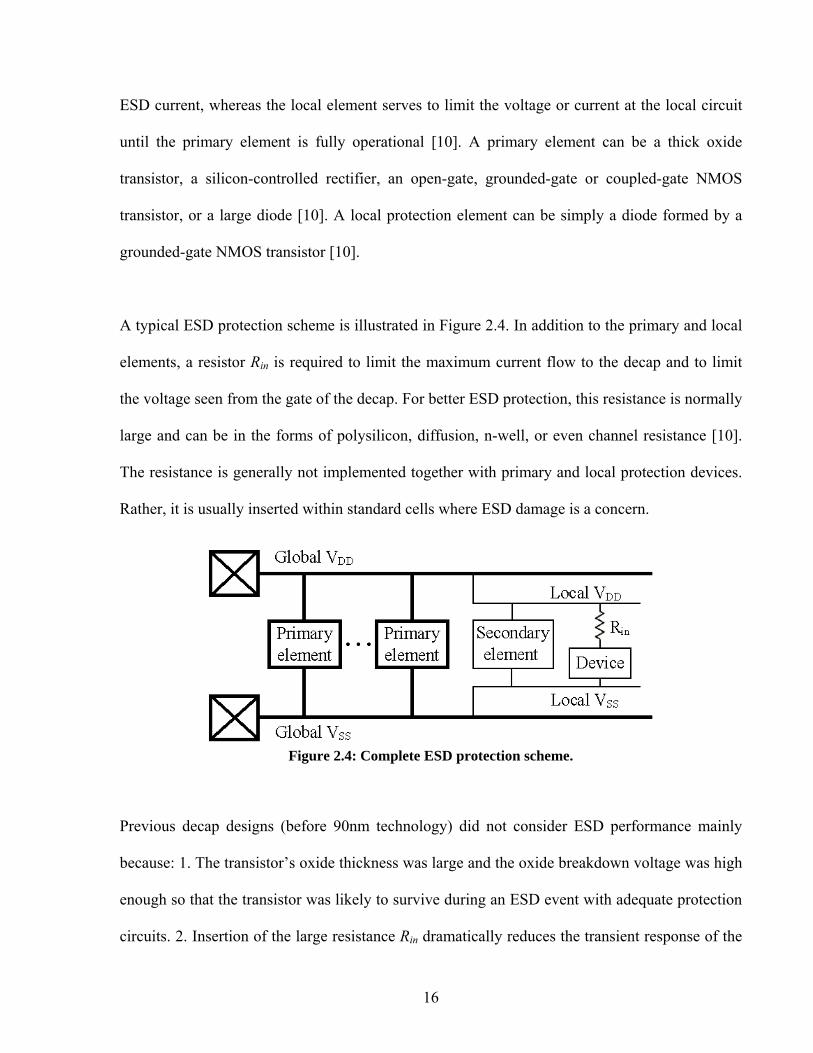
ESD current, whereas the local element serves to limit the voltage or current at the local circuit
until the primary element is fully operational [10]. A primary element can be a thick oxide
transistor, a silicon-controlled rectifier, an open-gate, grounded-gate or coupled-gate NMOS
transistor, or a large diode [10]. A local protection element can be simply a diode formed by a
grounded-gate NMOS transistor [10].
A typical ESD protection scheme is illustrated in Figure 2.4. In addition to the primary and local
elements, a resistor Rin is required to limit the maximum current flow to the decap and to limit
the voltage seen from the gate of the decap. For better ESD protection, this resistance is normally
large and can be in the forms of polysilicon, diffusion, n-well, or even channel resistance [10].
The resistance is generally not implemented together with primary and local protection devices.
Rather, it is usually inserted within standard cells where ESD damage is a concern.
Figure 2.4: Complete ESD protection scheme.
Previous decap designs (before 90nm technology) did not consider ESD performance mainly
because: 1. The transistor’s oxide thickness was large and the oxide breakdown voltage was high
enough so that the transistor was likely to survive during an ESD event with adequate protection
circuits. 2. Insertion of the large resistance Rin dramatically reduces the transient response of the
16

decap. However, starting from 90nm, the gate oxide is so thin that the designer cannot ignore the
increased ESD risk. A large resistance is therefore recommended to be placed inside the decap
cells to protect from potential ESD damage. As a consequence, this tradeoff between ESD
performance and transient response becomes the main decap design challenge in 90nm.
2.5 Standard-Cell Decap Layout and Placement
In white spaces, decaps are usually made of NMOS devices, as described in the early sections.
However, within standard cells, it is more convenient to make decaps using both types of NMOS
and PMOS to form a decap filler cell, as shown in Figure 2.5. This is because the n-well is
already implemented and usually reserved for PMOS devices. Only the lower half-cell area is for
NMOS devices [4].
Figure 2.5: Standard cell N+P decap configuration.
One sample standard-cell decap layout is illustrated in Figure 2.6. In the figure, the NMOS decap
occupies roughly the bottom half of the cell area, whereas the PMOS decap is located in the n-
well. The capacitor areas are the polysilicon gates placed on top of the channel regions of the
MOS transistors. For standard cells, the height of the cell is always fixed, and the designers can
only adjust the cell width. Once the cell width is determined, the size of the decap and the
17

capacitance of the decap are established. Figure 2.6 implies a large decap cell (measured in cell
width) with long channel transistors.
Figure 2.6: Sample layout of standard-cell N+P decap with no fingers.
The decaps laid out in this long-channel fashion have poor performance at high frequencies, as
discussed in Section 2.3. Therefore, a fingering technique is commonly used to improve the
frequency response. Figure 2.7 depicts the same decap cell but with two fingers.
Figure 2.7: Sample layout of standard-cell N+P decap with two fingers.
18

To model this N+P decap configuration, the overall impedance of two parallel RC circuits is
determined as _ __ _
1( ) //( )eff n eff peff n eff p
R RsC sC
+ +1 , and simplified as
_ _
_ _ _ _
1 _ _( )
eff n eff p
eff n eff p eff n eff p
R Rhigher order terms
R R s C C+ +
+ +.
For first-order hand calculations, the higher-order terms are negligible. Thus, the overall
effective capacitance is the sum of the two individual decoupling capacitances, and the overall
effective resistance is the parallel combination of the two individual effective resistances. That is:
(2.4) _ _ _ _//eff overall eff n eff p eff n eff pC C C C C≈ = + _
_ __ _ _
_ _
// eff n eff peff overall eff n eff p
eff n eff p
R RR R R
R R≈ =
+ (2.5)
During the placement procedure, computer-aided design (CAD) tools place standard cells into
rows. Because the height of each cell is always the same, when cells are placed adjacent to each
other, the n-well region and the VDD and VSS lines are automatically aligned. The cells for
placement are obtained from the standard-cell library, where all the cells are predefined in width
and driving strength. Since the total width of the row is fixed and the individual cell widths are
fixed, some empty spaces (typically small) between the cells are left after placing cells. Those
empty spaces are good candidates for the placement of decap cells due to its convenience [4]. In
fact, a set of decap cells with different cell widths is also implemented in the standard-cell library.
All the cells in the library must be designed for a specific process and meet all the design rules.
Routing is typically carried out right after placement.
19

Decap insertion is considered as a part of the complete design flow. In a typical ASIC design
flow, once the standard-cell blocks are synthesized, placed and routed by CAD tools, the decap
cells are naturally placed into the empty spaces. Generally, since the spaces are filled using a
library of decap cells with various sizes, the decap placement is done without affecting the
placement of other logic cells. After placement and routing, chip-level timing is analyzed and
timing violations will be fixed by replacement and/or rerouting. Then, chip-level voltage-drop
analysis is carried out by some CAD tools (e.g., Apache™ Redhawk™) such that the hot spots of
severe voltage-drop areas are identified. If the voltage drop at the hot spots exceeds the noise
budget, more decaps will be inserted into the violation regions and a modification of the
placement of other logic cells may have to be done. The logic cell movement requires additional
timing and routability analysis before moving on to next step. Then, the chip voltage drop is
analyzed again for the remaining hot spots. These steps in the design flow are iterated until all
the hot spots are eliminated and all the logic circuits pass timing analysis. Typically, it may take
1 or 2 (occasionally even more) iterations to eliminate all the hot spots [3]. In addition, the
potential problem of electromigration is also checked alongside the IR drop analysis [3].
This generally used decap placement approach is not optimal simply because the empty cells
may not be located near the high voltage-drop regions. After the hot spots are first identified, the
remaining empty spaces near the hot spots may not be largely enough. Hence, the logic cells may
have to be shifted, resulting in additional timing analysis. In order to improve the placement
efficiency, researchers suggest a few approaches including: global decap placement between
standard-cell blocks [21], decap placement using activity [7], standard-cell decap placement not
affecting relative placement of logic cells [2], and earlier-stage decap placement decision [4].
20

Since decaps are experiencing excessive gate leakage, decap placement methods considering
leakage current are proposed in [9] and [22].
21
Chapter 3
Existing Decoupling Capacitor Design Approaches
3.1 Introduction
Before 90nm technology, the use of MOS transistors as decoupling capacitors appeared to be a
straightforward solution to the decap design problem. However, many factors such as excessive
gate leakage, increased ESD risk, and consideration for high-performance transient response
come to play important roles from 90nm technology. The consequence is that the standard MOS
decap design may no longer be appropriate for the use in 90nm or below. Researchers have
provided some new design approaches to address the design issues for decaps. This chapter
provides an overview that sequences through all the major existing methodologies and identifies
their advantages and disadvantages.
3.2 Cross-Coupled Decap
Knowing that the standard N+P decap design for standard cells may no longer be suitable for
90nm technology due to increased ESD risk, a new cross-coupled decap design has been
proposed [11] to address this issue. In the new cross coupled design (Figure 3.1), the drain of the
PMOS connects to the gate of the NMOS, whereas the drain of the NMOS is tied to the gate of
the PMOS [11].
22

Figure 3.1: Cross-coupled decap schematic [11].
From the layout perspective, this cross-coupled circuit can be seen simply as a terminal-swapped
version of the standard decap. In other words, the decap transistor areas need not to be modified,
while only the metal wire connections are modified. Thus, this new design does not require
additional area in layout, compared to the standard design.
Both transistors in this design are still in the linear region. In the standard decap design, the gates
of the transistors are directly connected to either VDD or VSS, depending on the transistor type. In
this case, the gate of the NMOS device is connected to VDD through the channel resistance of the
PMOS device. Similarly, the gate of the PMOS device is tied the channel resistance of the
NMOS device and then connected to VSS. The added channel resistance to the gate provides the
input resistance Rin for ESD protection, as previously mentioned in Section 2.4. The input
resistance can help to limit the maximum current flow to the decap so that the voltage seen from
the gate of the decap is also limited.
Intuitively, the input resistance along with the decap can be thought as a low pass filter, as
illustrated in Figure 3.2. When there is a sudden voltage jump at the power line (Vin) during an
23

ESD event, the voltage at the gate of the decap (Vgate) does not increase instantaneously with the
increase of Vin. Instead, the increase of Vgate is delayed due to the low-pass RC effect. This time
delay in the voltage change at the transistor gate helps to protect the gate until the primary and
secondary ESD devices are fully operational and shunt the ESD current away. Hence, it is
desirable to have Rin as large as possible from the standpoint of ESD protection.
Figure 3.2: Intuitive understanding of input resistance in cross-coupled design.
By simply swapping the terminal connections, the cross-coupled design adds a considerably
large Rin to the gate of the decaps, without increasing the layout area. The tradeoff of this design
is the reduced transient performance as a decap.
Since both transistors are in the linear region, the two transistors are on and do not limit the gate
leakage current flow compared to the standard design. Hence, no savings in gate leakage are
achieved in this cross-coupled approach. This design nicely illustrates the concept of tradeoffs
between transient response and ESD reliability when designing a decap. This cross-coupled
circuit is also considered to be fairly passive and robust. In the next chapter, this circuit will be
discussed in greater detail, and modifications will be provided to address different design
tradeoffs including gate leakage. Two of the modification circuits can achieve higher gate
leakage savings and provide comparable or better transient response, while another is better in
terms of ESD reliability.
24
3.3 Gated Decap
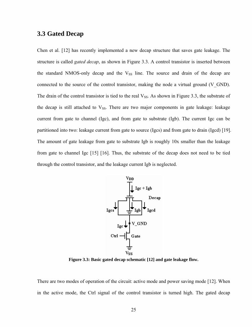
Chen et al. [12] has recently implemented a new decap structure that saves gate leakage. The
structure is called gated decap, as shown in Figure 3.3. A control transistor is inserted between
the standard NMOS-only decap and the VSS line. The source and drain of the decap are
connected to the source of the control transistor, making the node a virtual ground (V_GND).
The drain of the control transistor is tied to the real VSS. As shown in Figure 3.3, the substrate of
the decap is still attached to VSS. There are two major components in gate leakage: leakage
current from gate to channel (Igc), and from gate to substrate (Igb). The current Igc can be
partitioned into two: leakage current from gate to source (Igcs) and from gate to drain (Igcd) [19].
The amount of gate leakage from gate to substrate Igb is roughly 10x smaller than the leakage
from gate to channel Igc [15] [16]. Thus, the substrate of the decap does not need to be tied
through the control transistor, and the leakage current Igb is neglected.
Figure 3.3: Basic gated decap schematic [12] and gate leakage flow.
There are two modes of operation of the circuit: active mode and power saving mode [12]. When
in the active mode, the Ctrl signal of the control transistor is turned high. The gated decap
25

operates almost like the standard decap, except that there is a small channel resistance of the
control transistor. The size of the control transistor needs to be large to have the channel
resistance small since a large resistance will reduce the transient response of the decap. When in
power saving mode, the Ctrl signal is turned low so that the control transistor operates in the
subthreshold regime. The node V_GND can be considered a virtual ground (floating), where the
voltage at V_GND can be determined by the series resistance of Reff of the decap and the channel
resistance of the control transistor. In this configuration, the gate leakage saving is projected to
be 99% in a 70nm process [12].
The basic idea of the gated decap is from multi-threshold CMOS (MTCMOS). The control
transistor comes from the concept of the sleep transistor in MTCMOS. As expected, the control
transistor should have a high VT to keep the subthreshold leakage small. The largest challenge of
this gated decap would be the proper selection of the Ctrl signal. At the top level, the Ctrl signal
can be driven by the hardware/software interface. When there is no activity in the system, the
operating system (software) will set up the signal to force the chip into power saving or standby
mode. From the hardware architectural level, the Ctrl signal can be managed by some self-
predictive architecture [12] [23]. At the circuit level, it is desired that the gated decap is self-
maintained, and no external circuitry is required to control it on or off. In that case, it may need
to have a special clock, as shown in Figure 3.4. Before the regular clock rises, the Ctrl signal can
be set high to allow some setup time for the decap to fully setup. When the regular clock falls,
the Ctrl signal can also fall simultaneously to save power. The time period when the Ctrl signal is
low can be considered as the power saving period.
26

Figure 3.4: Sample clock for the Ctrl signal in gated decap.
Another substantial difficulty is oscillation. It was observed in [12] that the voltage levels at the
local power lines oscillate when the gated decap is turned on or off. The reason is that sharp rises
and falls in the Ctrl signal get passed through the decap and hence make the power lines noisy.
The oscillation level is determined to be excessive: more than 10% of VDD of the simulation
process [12]. Such large oscillation is certainly non-acceptable and some form of modification
has to be taken.
The solution of reducing excessive oscillation provided in [12] is to insert a small-size inverter,
as shown in Figure 3.5. Sharp rising and falling edges in the Ctrl signal correspond to the
concept of large slew rate. The insertion of the small inverter helps reduce the slew rate at Ctrl.
Figure 3.5: Insertion of small inverter in gated decap [12].
27
The gated decap is a good attempt in solving the problems of excessive gate leakage for decap
designs. Nonetheless, the design style is not conservative enough so that it experiences many
issues such as oscillation. In other words, the robustness of this gated decap may not be good
enough to implement in industrial designs.
3.4 Thick Oxide Decap
Fabrication foundries usually provide high-voltage, thick-oxide MOS devices in a CMOS
process. The thick-oxide devices are intended for the use in I/O interfaces and other places where
a higher voltage supply is present. Typically, for a 90nm process, the nominal VDD is scaled to
1.0V, while the thick devices can still hold for 3.3V voltage level [24]. Similarly, for a 130nm
process, with a nominal power supply of 1.2V, the high voltage for the thick-oxide transistors is
3.3V [25].
For thick-oxide devices in a 90nm process [24], the oxide is roughly 3x thicker than the thin-
oxide devices, resulting in 3x higher oxide breakdown voltage. Moreover, because of the
exponential relationship between tox and Jgate_leak given in Equation (2.3), the gate leakage of such
thick-oxide devices in 90nm is almost zero, which is also consistent with SPICE simulations.
Hence, the use of thick-oxide transistors can eliminate the concerns of ESD reliability and gate
leakage completely.
The largest disadvantage of thick-oxide devices is that the effective capacitance Ceff is reduced
by roughly 1/3. Moreover, it is difficult to place thick-oxide devices within a standard-cell block.
The thick-oxide decaps must be properly placed around the periphery of the block. The use of
28

thick decaps is only suggested in the open areas between blocks when both ESD risk and gate
leakage need to be minimized and while there is also a high demand on transient response
performance. Under such scenarios, the 3x area penalty may have to be paid.
To complete the concept of thick-oxide decaps, there is a similar situation where a stack of thin-
oxide decaps is used, as shown in Figure 3.6. Assuming a 90nm process has a 1.0V power supply
and a threshold voltage VT of 0.3V, VT is roughly at VDD/3. Stacking three thin-oxide decaps in
series results in the gate voltage difference VOX across each decap to be VDD/3. As mentioned in
Section 2.3, gate leakage is a function of biasing voltage. If VOX is in the subthreshold region
(close to VT), the leakage current is 3-6 orders of magnitude less than the leakage current in
strong inversion. Namely, biasing the decap in the subthreshold region will have negligible gate
leakage. The disadvantage of this approach is also similar to that of thick-oxide devices: it
serializes 3 decaps and has therefore a resulting equivalent capacitance of 1/3 of one decap. Thus,
in order to provide certain amount of decoupling capacitance, much more areas (~9x) are needed
in this fashion.
Figure 3.6: Stack of thin-oxide decaps versus thick-oxide decap.
29

Showing the idea of the stacked thin-oxide decaps is only to further illustrate the concept of
using thick-oxide devices. Stacking thin-oxide decaps does not have practical applications due to
its large area requirement.
3.5 High-k Gate Dielectric
The oxide capacitance COX is a critical factor to many physical properties of MOS transistors.
The drain current IDS of a transistor is proportional to COX. A larger COX results in a larger drain
current and hence a faster transition or a shorter gate delay [3]. Also, the subthreshold leakage
including drain-induced barrier lowering (DIBL) is related to COX. A larger COX corresponds to
smaller subthreshold leakage and less DIBL effect [15]. As a consequence, each technology
generation attempts to increase COX by roughly 1.4x while reducing the channel length L to 0.7x
of the previous technology’s channel length. The result is that the product of has been
maintained constant for over 25 years [3] as technology scales. The increase in COX balances the
tradeoff between the drain current and the subthreshold leakage current in each technology node.
OXC L
From Equation (2.3), the gate leakage density is inversely related to tOX. A smaller tOX leads to
exponentially increasing gate leakage. From the gate leakage perspective, the oxide thickness tOX
should be kept large. However, the oxide capacitance per unit area, COX, is determined by [3]:
OXOX
OX
Ctε
= (3.1)
where εOX is the permittivity of the oxide and is fixed for a given oxide material. Equation (3.1)
suggests that if εOX is kept unchanged, the increase in COX will lead to certain decrease in tOX and
hence exponential growth in gate leakage.
30

Knowing that the gate leakage increase may be excessive for 90nm technology and below, in
order to keep tOX thick while increasing COX, one can adjust the relative dielectric constant, k,
where 0OX kε ε= ⋅ , and 0ε is the vacuum permittivity. If a high permittivity (high-k) dielectric
can be used instead of the normal SiO2 oxide, the physical oxide thickness tOX would no longer
be limited by its electrical property COX. This concept of using high-k dielectrics was first
presented in [26], and researchers and process engineers have continued to pursue better high-k
materials [27]. Most experts agree that high-k gate dielectrics will help to keep the gate leakage
under control [27].
Commonly suggested high-k materials include HfO2, ZrO2, and Al2O3 [27]-[29], whose
permittivity ranges from 10 to 30, compared to 3.97 of SiO2. [30] presents the materials of
barium titanate (BTO) and barium strontium titanate (BSTO) that have permittivity ranged from
100 to 400, about the highest among the up-to-date research results.
The application of high-k gate dielectrics is currently an active research area. Many challenges
still remain [27]: thermal stability of the dielectrics, interfacial layer formation, effective oxide
thickness control and environmental sensitivity, channel mobility degradation, high-k dielectric
stability with poly-silicon gates, and possible use of metal gate instead of poly-silicon. Among
all, the two most critical problems are: (1) High-k and polysilicon gates are incompatible due to
Fermi level pinning at the interface between high-k and polysilicon, which causes high threshold
voltages in transistors. (2) The high-k/polysilicon transistor structure exhibits a degradation of
31

channel mobility μ due to Coulombic scattering since high-k MOSFETs tend to have more oxide
charge and interface traps [27] [29].
Until the majority of the above mentioned issues are solved, high-k dielectrics may not be
applied to industrial designs. [31] predicts the availability of high-k technology in the year 2007.
At least for now, for a typical 90nm process [24], the oxide material still uses regular SiO2,
which was also the case for the 130nm technology.
3.6 Metal-Insulator-Metal Capacitor
Many fabrication processes support the implementation of metal-insulator-metal (MIM)
capacitors. MIM capacitors can be integrated into both aluminum and copper interconnect
backend of the line (BEOL) processes [32]. In an Al process, a MIM capacitor is usually
composed of an Al bottom plate with Ti or TiN liners, a silicon dioxide SiO2 or silicon nitride
Si3N4 dielectric, and a titanium nitride TiN top plate [33] [34]. For Cu processes, various MIM
integration schemes have been reported for the past few years by several research groups [34].
The materials of metal electrodes and dielectrics in use vary from case to case [34]. Typically, in
a Cu process, a MIM capacitor is composed of a Cu (or Ta or TaN) bottom place, a plasma-
etched chemical vapor deposition SiN dielectric, and a Ta top electrode [34] [35]. MIM capacitor
designs typically utilize the top metal layer and the next lower metal plate as the two capacitor
electrodes in order to minimize the parasitic coupling capacitance between the bottom of the
MIM plate and substrate [33].
32

MIM capacitors are popular in analog, mixed-signal, and RF IC designs, mainly because of high
linearity, low series resistance, high capacitance density, high precision, and low parasitic
capacitance [33]. The depletion-free, highly-conducting metal electrodes are suitable for high
speed applications at low cost [34]. In addition, MIM capacitors usually have small leakage
currents, mainly because the dielectric thickness is large (>50nm) [33]. The low effective
resistance and low leakage make MIM capacitors good candidates for white-space decaps. When
connecting to the MIM capacitors, the interconnects need to be kept short and wide so that the
total resistance is maintained low [35].
3.7 Summary
This chapter described a number of design approaches for decaps in recent technologies. Starting
from circuit level, cross-coupled decap, gated decap, and thick-oxide decaps are discussed in
details. Process level efforts are also taken into account, where the use of high-k gate dielectrics
and MIM capacitors is addressed. Moreover, researchers are implementing decaps in special
MOS structures [36] and claiming good results in gate leakage savings. Another circuit design
approach, called switched decap, is more complex and will be discussed separately in Chapter 5.
As already mentioned, decap design with gate leakage consideration is still an active field
because the problem of excessive gate leakage is fairly new. In order to make further
improvements from the existing design approaches, the cross-coupled design is investigated in
this research since it is commonly used in 90nm standard-cell libraries.
33

Chapter 4
Passive Decoupling Capacitor Designs
4.1 Introduction
The objective of this chapter is to provide passive decoupling capacitor designs that properly
tradeoff between their transient response, ESD performance, and gate leakage. The basic idea of
the cross-coupled decap is to use a crossly coupled N+P decap pair to reduce ESD risk by adding
series resistances to the gates. Continuing on from the discussion in Section 3.2, modeling of the
cross-coupled decap is provided. Before any improvements can be made, detailed transient, ESD
and gate leakage simulations have to be setup and carried out to compare against the standard
decap. After the quantitative analysis of the advantages and limitations, three modifications
based on the basic cross-coupled design are then proposed in [37] and [38]. One sample cell
layout for each of the modified circuits is provided. From the simulation results,
recommendations are made as to how to select the appropriate design for a given technology or a
process.
4.2 RC Modeling of Basic Cross-Coupled Decap Design
Knowing that the standard N+P decap design may no longer be suitable for 90nm technology
due to the increased ESD risk, a cross-coupled decap design has been proposed [11] to address
34

the issue of ESD reliability. It reconnects the terminals of the two transistors: the drain of the
PMOS connects to the gate of the NMOS, whereas the drain of the NMOS is tied to the gate of
the PMOS [11].
Figure 4.1: Cross-coupled decap schematic [11] and modeling.
The design can be modeled as a series connection of Reff and Ceff, similar to the standard decap,
as illustrated in Figure 4.1. The overall Ceff is roughly the same, while the overall Reff increases
significantly. Both transistors are still in the linear region, but the channel resistance is modified.
Specifically,
(4.1) _ _ _ _//eff overall eff n eff p eff n eff pC C C C C≈ = + _
__ _ _ _( ) //( )eff overall eff p on n eff n on pR R R R R≈ + +
_ __ _
_ _
// on n on pon n on p
on n on p
R RR R
R R≈ =
+ (4.2)
where Ceff_n, Ceff_p, Reff_n and Reff_p are the intrinsic effective capacitances and resistances,
respectively, and Ron_p and Ron_n are the channel resistances of the two transistors. Since Ron_p
and Ron_n are at least one order of magnitude larger, Reff_p and Reff_n can be neglected in the
overall Reff calculation. Here,
on eqLR R
W≈ (4.3)
35

where Req is the process-dependent square resistance (kΩ/). It is important to realize that
Equation (4.1)-(4.3) are first-order, low-frequency approximations only. The real transistor
channel resistance by nature is nonlinear and depends strongly on applied voltages, operating
frequency, and geometry [3]. The only reason for providing these formulae is to give designers
some insight into the design tradeoffs.
This cross-coupled design improves the ESD performance of the decap by making the overall
effective resistance larger without adding additional area. The tradeoff of the design is a reduced
transient response. The larger Reff corresponds to a longer RC delay. In addition, this design
provides no savings in gate leakage as compared to the standard design.
To quantitatively measure ESD performance, transient response, and gate leakage, a number of
simulations were carried out. The layouts were created in Virtuoso™ Layout Editor, verified by
Calibre™ DRC checker, and then extracted by Calibre XRC parasitic extraction tool. The
extracted data were simulated with HSPICE™ for different simulation setups. For fairness, the
same cell area was used for all the designs.
4.3 Transient Response Simulation
In order to carry out some simple but efficient transient simulations, the setup in Figure 4.2 was
chosen to evaluate the time domain decap performance. The setup is a pessimistic situation
where no power supply is present. Only the decap provides the needed current to charge up the
load when the inverter switches. The node V* is initially charged to VDD, and the output is
initialized to 0V while the total switched capacitance Cswitched is set to roughly 1/10 of the
36

decoupling capacitance and then fixed. Note that Cswitched includes the output parasitic
capacitance of the inverter. The input of the inverter is initially set to VDD. At 30ps, it starts to
drop linearly from VDD to 0V, reaches 0V at 60ps, and then remains constant.
Figure 4.2: Schematic for the first transient setup.
To simplify this transient setup, the decap can still be treated as series of Reff_overall and Ceff_overall,
as shown in Figure 4.3. The values of Reff_overall and Ceff_overall would be different for cross-
coupled and standard decaps.
Figure 4.3: RC modeling of the first transient setup.
It is possible to gain insight into the required Ceff_overall value obtained from the final V* voltage.
When the transient analysis runs for sufficient long time (>1ns), the voltage level at V* stabilizes.
Applying the charge-sharing equation, the final voltage V* can be derived as a function of
Ceff_overall, as follows:
_ _ * *before after
eff overall DD eff overall switched
Q Q
C V C V C V
=
= +
37

_
_
* eff overallDD
eff overall switched
CV
C C⎛ ⎞
= ⎜⎜ +⎝ ⎠V⎟⎟ (4.4)
If the decap has a large Ceff_overall, which is desired, the final V* value will be also large and close
to the initially charged value VDD.
One step of further simplification of this circuit can be used to understand the significance of
Reff_overall of the decap. For this purpose, the Reff_overall and Ceff_overall are both assumed to be fixed.
Also, the ‘1’ to ‘0’ ramp transition that the inverter switches is replaced by a pulse, meaning that
there is no time delay from VDD to 0 when the inverter switches. Since the NMOS device in the
inverter can be assumed off during the transition, it can be neglected from the model. The
switching of the PMOS device in the inverter is simplified as a constant channel resistance of
Rp_channel. Therefore, the circuit can be modeled as shown in Figure 4.4.
Figure 4.4: Simplification of RC modeling of the first transient setup.
After applying Laplace transform to the circuit in Figure 4.4, the voltage at V* can be expressed
in the s-domain as a simple voltage divider:
_
_ __
1
*( ) 1 1
P channelswitched DD
P channel eff overallswitched eff overall
RsC VV s
sR RsC sC
+= ⋅
+ + +
38

_ _ _
_ _ _
_
_ _
( )( )(
*( )
(
eff overall P channel switched eff overall eff overallDD DD
eff overall switched eff overall switched eff overall P channel
eff overall switched
eff overall switched eff overal
C R C R CV V
C C C C R RV s C Cs s
C C R
_
_ )−
+ += +
++
+
_ )l P channelR+
(4.5)
Applying the inverse-Laplace transform, the time-domain voltage V* is (for t > 0):
_
_
*( ) ( ) ( )eff overallDD
eff overall switched
CV t V u t
C C= ⋅ +
+
_
_ __
( )(_ _ _
_ _ _( )( )
eff overall switchedeff overall P channel
eff overall switched
tC C
R RC CP channel switched eff overall eff overall
DDeff overall switched eff overall P channel
R C R CV e
C C R R
−+
+−⋅
+ +
)
(4.6)
Here, the final voltage V* is consistent with the simple charge-sharing calculation. The time
constant associated with V* is __ _
_
( )( eff overall switchedeff overall P channel
eff overall switched
C CR R
C C+
+) , the serial combination
of Reff_overall and Rp_channel multiplied by the serial combination of Ceff_overall and Cswitched. The
effective overall resistance Reff_overall of the decap should be made small so that this time constant
will also be small.
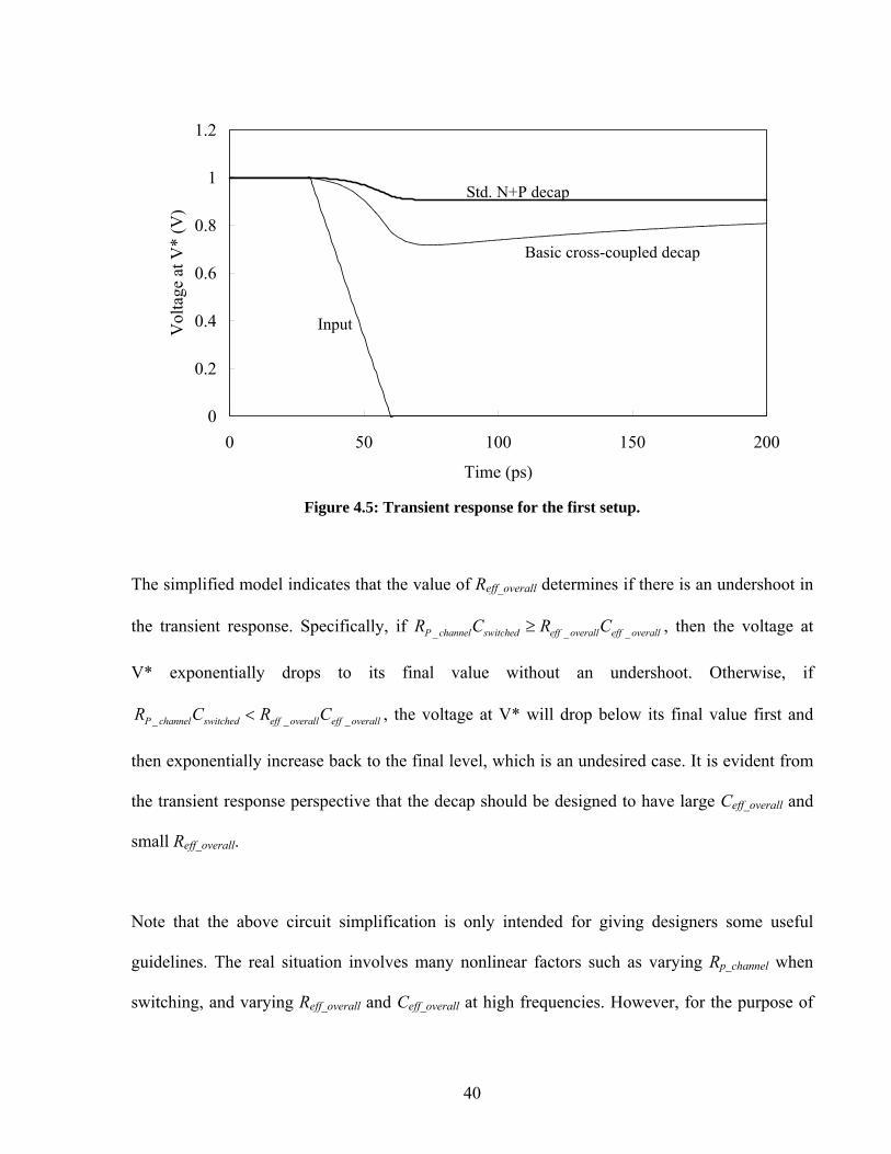
HSPICE simulation for this setup is illustrated in Figure 4.5, where the response of the two
designs is plotted. Although not shown, the hand calculation can generate curves that are close to
the SPICE results, as expected. From the figure, the two designs have close effective capacitance
because their final voltage levels at V* are close. On the other hand, the cross-coupled design
experiences larger Reff_overall, resulting in an undershoot and faster voltage drop as input switches.
Clearly, the standard decap can provide much better transient response.
39
0
0.2
0.4
0.6
0.8
1
1.2
0 50 100 150 200
Time (ps)
Vol
tage
at V
* (V
)
Input
Std. N+P decap
Basic cross-coupled decap
Figure 4.5: Transient response for the first setup.
The simplified model indicates that the value of Reff_overall determines if there is an undershoot in
the transient response. Specifically, if _ _ _P channel switched eff overall eff overallR C R C≥ , then the voltage at
V* exponentially drops to its final value without an undershoot. Otherwise, if
_ _ _P channel switched eff overall eff overallR C R C< , the voltage at V* will drop below its final value first and
then exponentially increase back to the final level, which is an undesired case. It is evident from
the transient response perspective that the decap should be designed to have large Ceff_overall and
small Reff_overall.
Note that the above circuit simplification is only intended for giving designers some useful
guidelines. The real situation involves many nonlinear factors such as varying Rp_channel when
switching, and varying Reff_overall and Ceff_overall at high frequencies. However, for the purpose of
40

first-order calculations or estimations, the simplified model gives valuable insight into the design
tradeoffs.
Another simple setup was also used to determine the effective capacitance value and the RC
delay of the decap. The setup is shown in Figure 4.6. The VDD node is connected to the nominal
supply of 1V (for 90nm), and VSS is tied to a common ground. When there is no activity, the
current flow from VDD to VSS is solely due to gate leakage. At 1ns, VDD starts to drop linearly
from 1V to 0.9V, reaches 0.9V at 2ns, and then remains constant.
Figure 4.6: Schematic for the second transient setup.
By definition, an ideal capacitor responds to a voltage change as a current source if it is fully
charged, as follows [39]:
decap decap decapdv vI C Cdt t
Δ= ≈
Δ (4.7)
If the voltage change is a ramp, the current provided by the ideal capacitor should be a pulse. In
practice, due to the presence of the effective resistance associated with the decap designs, a
certain amount of RC delay exists. A good transient response should have sharp rise and fall
edges (at 1ns and 2ns in this case), and also provide a large average current Iavg during the time
period from 1ns to 2ns. The sharpness of rise and fall is measured from the rise/fall slopes with a
41

unit of A/s. The average capacitance Cavg is calculated from Iavg from Equation (4.7). Figure 4.7
illustrates the curves for the two designs in transient analysis, and indicates that the standard
decap is better in the transient response. The result in this plot is consistent with the result
obtained from Figure 4.5 previously.
-1
0
1
2
3
4
5
6
0.0 1.0 2.0 3.0 4.0 5.0
Time (ns)
Idec
ap C
urre
nt (u
A)
Std. N+P decap
Basic cross-coupled decap
Figure 4.7: Transient response for the second setup.
4.4 ESD Performance Simulation
The ESD simulation requires an ESD generation model. Among all the existing models, the
human body model (HBM) was adopted for simplicity. Following the standard MIL-STD-883x
method 3015.7 [10], a human body can be simulated as a series of 1.5kΩ resistance RHBM and
100pF capacitance CHBM. The capacitor CHBM is initially charged to 2kV that needs to be
discharged through some primary elements. The primary element is arbitrarily chosen to be an
42
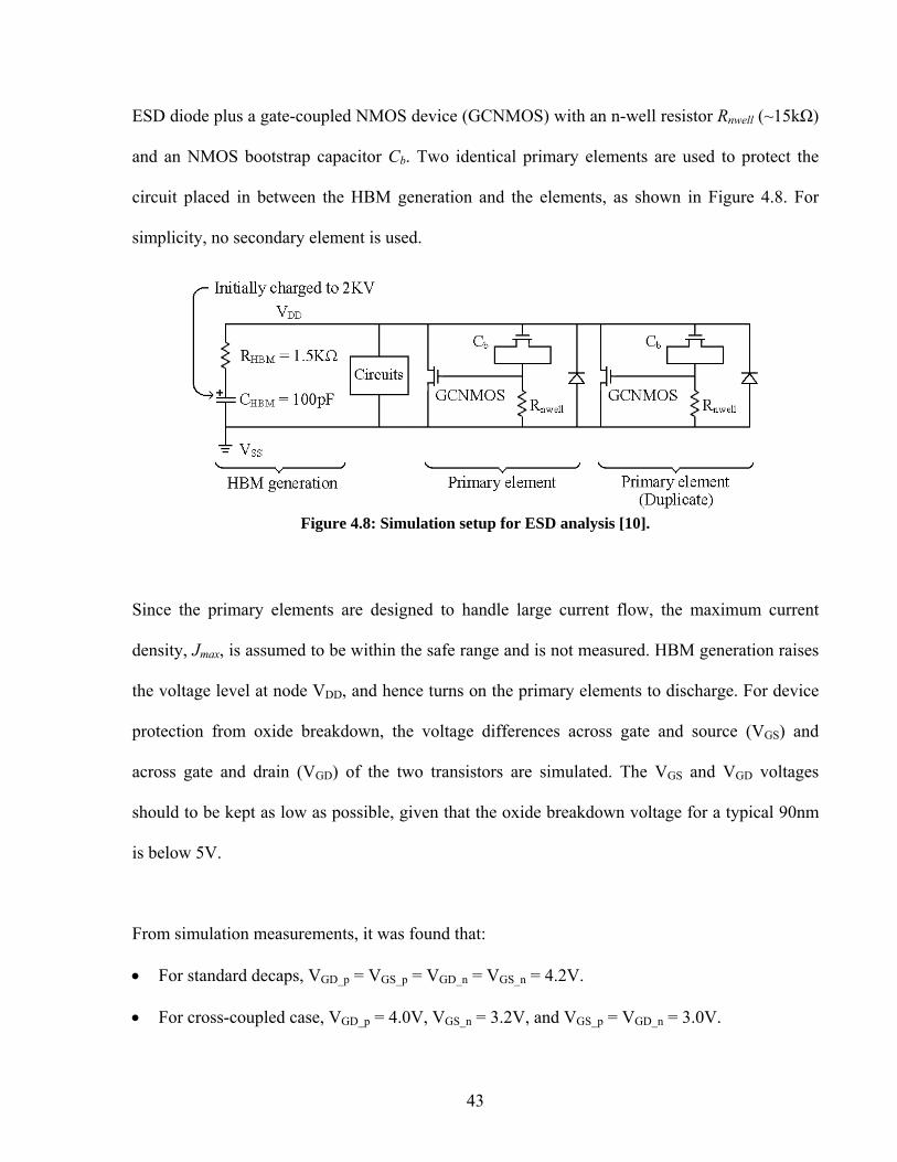
ESD diode plus a gate-coupled NMOS device (GCNMOS) with an n-well resistor Rnwell (~15kΩ)
and an NMOS bootstrap capacitor Cb. Two identical primary elements are used to protect the
circuit placed in between the HBM generation and the elements, as shown in Figure 4.8. For
simplicity, no secondary element is used.
Figure 4.8: Simulation setup for ESD analysis [10].
Since the primary elements are designed to handle large current flow, the maximum current
density, Jmax, is assumed to be within the safe range and is not measured. HBM generation raises
the voltage level at node VDD, and hence turns on the primary elements to discharge. For device
protection from oxide breakdown, the voltage differences across gate and source (VGS) and
across gate and drain (VGD) of the two transistors are simulated. The VGS and VGD voltages
should to be kept as low as possible, given that the oxide breakdown voltage for a typical 90nm
is below 5V.
From simulation measurements, it was found that:
• For standard decaps, VGD_p = VGS_p = VGD_n = VGS_n = 4.2V.
• For cross-coupled case, VGD_p = 4.0V, VGS_n = 3.2V, and VGS_p = VGD_n = 3.0V.
43
The cross-coupled design provides better ESD protection by making the overall effective
resistance larger without adding additional area. However, the improved ESD performance is at
the expense of transient response, as described earlier.
4.5 Gate Leakage Simulation
The gate leakage levels can be obtained from the two transient setups in Section 4.3. In the first
transient setup (Figure 4.2), before the inverter switches, the static current flow through the
decaps can be treated purely as gate leakage. In the second transient analysis (Figure 4.6), before
the node VDD starts to drop its voltage, the current flow through the decaps is solely gate leakage.
When carrying out SPICE simulations, it is essential to use BSIM4 version to have gate leakage
models built-in [14]. Earlier BSIM versions do not support gate leakage models [14]. The gate
leakage in BSIM4 is partitioned into two parts: the tunneling current between gate and substrate
(Igb) and the current between gate and channel (Igc) [19]. Since the current Igb is considerably
smaller than Igc, Igb is set off by default [24]. To make sure both current components are set on
for the best accuracy, two selectors, IGBMOD and IGCMOD, need to be set ‘1’ [19].
As discussed in the earlier sessions, the cross-coupled decap design does not provide any savings
in gate leakage. HSPICE simulations show that the two designs have almost identical gate
leakage: 53.8nA for the standard decap and 53.7nA for the cross-coupled design.
44

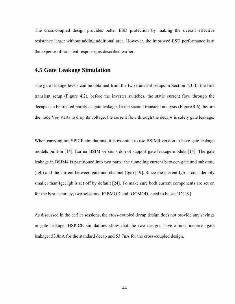
4.6 Modified Cross-Coupled Decap Designs
Three modifications are made to address different goals of decap design: ESD performance,
transient response, and gate leakage. It is difficult to simultaneously make improvements on all
the three goals, but trying to balance them and to make tradeoffs is certainly feasible and indeed
achievable. Each modification is compared to the basic cross-coupled design to show advantages
and disadvantages. Again, the total cell area is fixed for all the designs.
The first modification (Mod1) attempts to improve ESD performance by making the channel
lengths of the two resistors longer (Figure 4.9). The two fingers are combined into one. As a
result, the overall Reff is almost doubled, while the overall Ceff remains roughly the same. The
disadvantage of this design is reduced transient response and slightly larger gate leakage since
the gate area increases a little.
Figure 4.9: Sample layout of Mod1 (basic circuit without fingering).
The second modification (Mod2) attempts to reduce gate leakage while maintaining ESD
performance and transient response at roughly the same level (Figure 4.10). One NMOS is
replaced by a PMOS with the n-well expanded to accommodate the new PMOS. The effect of
45

this change is then increased Ron_p and Ceff_p. To match ESD performance, Ron_n needs to be
reduced. One simple change to obtain a small Ron_n is to reduce the channel length of the NMOS.
By the same token, Ceff_n is also reduced. The result is comparable ESD performance and
transient response if carefully designed. Using the fact that the new same-area PMOS leaks 3
times less than the replaced NMOS, extra saving in gate leakage is realized.
Figure 4.10: Sample layout of Mod2 (replace NMOS with PMOS).
The third modification (Mod3) (Figure 4.11) follows the similar approach as of Mod2. It further
increases the new PMOS area while reducing the NMOS area. Indeed, the minimum length
NMOS is used to obtain the smallest possible Ron_n so that it dominates and makes the overall Reff
smaller. Since the overall Reff is greatly decreased while the overall Ceff is somewhat higher, the
transient response dramatically improves. The only downside is reduced ESD protection
capability due to the reduced overall Reff.
46

Figure 4.11: Sample layout of Mod3 (replace NMOS with PMOS, and use smallest NMOS).
Table 4.1: Comparison on ESD performance, transient response and gate leakage.
ESD performance with 2
primary elements Transient response
Gate
leakage
First
setup Second setup
VGD_p (V) VGS_n (V)VGS_p =
VGD_n (V)Voltage
drop rate
(V/ns)
Rise
slope
(A/s)
Avg. cap
(fF)
Leakage
current
(nA)
Std. Decap 4.2 4.2 4.2 -1.8 2.8e5 54.3 53.8
Cross-
coupled 4.0 3.2 3.0 -5.4 8.2e4 33.1 53.7
Mod1 3.8 2.9 2.8 -5.3 8.7e4 21.4 59.7
Mod2 4.0 3.7 3.4 -8.6 7.0e4 35.8 33.6
Mod3 4.1 3.9 3.8 -7.0 1.1e5 47.5 31.8
Following the same simulation procedures outlined earlier, Table 4.1 summarizes the
comparisons for all the designs on ESD performance, transient slope response, and gate leakage.
The bold numbers indicate the best results in the comparison. The standard decap provides the
best transient response. Mod1 provides the best ESD protection, while Mod3 provides the lowest
47
gate leakage. One can view Mod2 as a compromise between Mod1 and Mod3. The complete
transient simulations for the first and second setups are also depicted in Figure 4.12 and Figure
4.13, respectively.
0
0.2
0.4
0.6
0.8
1
1.2
0 50 100 150 200
Time (ps)
Vol
tage
at V
* (V
)
Std. N+P decap
Mod3
Mod2
Mod1
Basic cross-coupled decapInput
Figure 4.12: Complete transient response for the first setup.
48

-1
0
1
2
3
4
5
6
0.0 1.0 2.0 3.0 4.0 5.0
Time (ns)
Idec
ap C
urre
nt (u
A)
Std. N+P decap
Mod3
Mod2 Basic cross-coupled decap
Mod1
Figure 4.13: Complete transient response for the second setup.
There is no single design that is optimal for all the possible specifications. The reason for having
several design options is to provide designers with different solutions so that they can make
suitable tradeoffs for a specific process at a specific technology node. For 90nm technology, the
standard decap still seems to be acceptable in ESD reliability, assuming the power rails have
protection elements. However, Mod3 is more suitable because it has better ESD performance and
saves roughly 41% on gate leakage. The only tradeoff then is a slightly reduced transient
response. As technology further scales, or as a different process increases the transistor speed,
the oxide thickness will probably become thinner and the oxide breakdown voltage will occur.
Under that scenario, the standard design or the Mod3 will no longer be appropriate. For
improved ESD performance, Mod2 is recommended instead of the basic cross-coupled design.
The reason is that Mod2 has similar ESD numbers and similar transient response compared to
the basic cross-coupled design but saves approximately 40% on gate leakage. When technology
49

scales down to a point that the oxide thickness makes the ESD reliability a more serious concern,
the use of Mod1 will be advised for the best ESD performance, although its transient response
will be sacrificed significantly.
The recommendations above are good for moderate or low frequency chips. If the targeting
frequency is extremely high, even Mod3 may not be able to provide desired amount of current
within an excessively small period of time. Under such a case, the use of thick-oxide decaps is
suggested around the standard-cell blocks. As mentioned in Section 3.4, for 90nm technology,
the oxide is 3x thicker than the thin oxide, resulting in almost zero gate leakage and 3x ESD
breakdown voltage. The disadvantage is the effective capacitance reduced to 1/3. Hence, the area
needed for a fixed capacitance is 3x for thick-oxide decaps. The thick-oxide decaps must be
properly placed around the periphery of the block. The fabrication cost for using thick-oxide
devices may also be slightly higher, although it may be needed for I/O and other features.
As technology further scales to 45nm or below, the gate oxide will probably become ultra thin
and will dramatically increase the ESD risk and the amount of gate leakage. The use of the cross-
coupled design and its modifications in this chapter will be eventually limited. The anticipation
at this stage would be the use of high-k gate dielectrics as the oxide materials so that the
electrical thickness and the physical thickness can be differentiated to completely eliminate the
concerns of ESD reliability and gate leakage. Other approaches would be to utilize MIM
capacitors as decaps or some other innovative structures, as discussed earlier. In any case,
solutions that properly balance gate leakage, ESD, transient response and area will be required.
50

Chapter 5
Active Decoupling Capacitor Designs
5.1 Introduction
Passive decaps described previously have a small layout and are useful within the standard cells.
However, for large global decaps (i.e., outside the block), other approaches can be used. This
chapter investigates active decap design approaches at the circuit level that help reduce voltage
variation on the global power grid. Specifically, the design of switched decoupling capacitors, as
power grid voltage regulators or stabilizers, will be studied here. The switched decaps amplify
the charge storage capacity of the basic decap while monitoring the power rail activity to provide
dynamic control of the switching response. The switched decaps have better area efficiency,
compared to the passive designs. The design complexity of switched decaps is much higher than
those discussed in Chapter 3. As a consequence, these designs are separated out and analyzed in
this chapter.
There are two designs that use switched decaps: a voltage regulator (VR) from Sun™ [40] [41]
and an active power stabilizer (APS) from Fujitsu™ [42]. The objective in this chapter is to
evaluate the two designs to replace the global thick-oxide decaps with better voltage regulation
capability. After a full understanding of the advantages and limitations of the two designs, a new
51
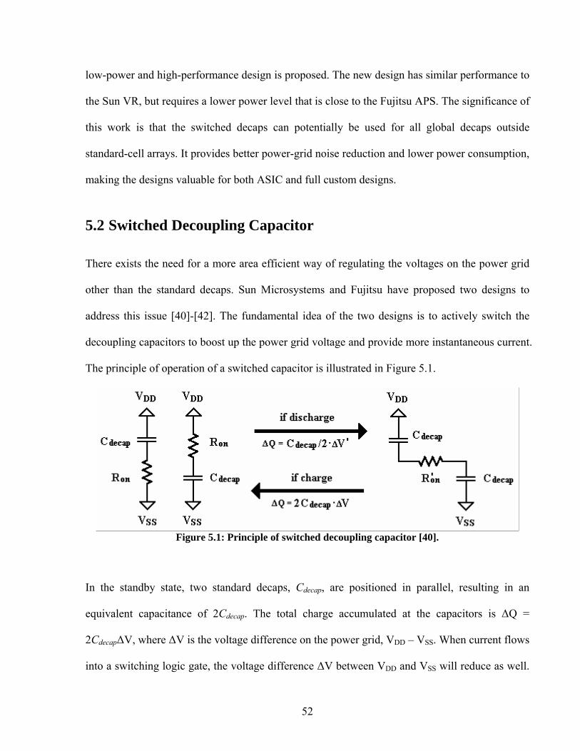
low-power and high-performance design is proposed. The new design has similar performance to
the Sun VR, but requires a lower power level that is close to the Fujitsu APS. The significance of
this work is that the switched decaps can potentially be used for all global decaps outside
standard-cell arrays. It provides better power-grid noise reduction and lower power consumption,
making the designs valuable for both ASIC and full custom designs.
5.2 Switched Decoupling Capacitor
There exists the need for a more area efficient way of regulating the voltages on the power grid
other than the standard decaps. Sun Microsystems and Fujitsu have proposed two designs to
address this issue [40]-[42]. The fundamental idea of the two designs is to actively switch the
decoupling capacitors to boost up the power grid voltage and provide more instantaneous current.
The principle of operation of a switched capacitor is illustrated in Figure 5.1.
Figure 5.1: Principle of switched decoupling capacitor [40].
In the standby state, two standard decaps, Cdecap, are positioned in parallel, resulting in an
equivalent capacitance of 2Cdecap. The total charge accumulated at the capacitors is ΔQ =
2CdecapΔV, where ΔV is the voltage difference on the power grid, VDD – VSS. When current flows
into a switching logic gate, the voltage difference ΔV between VDD and VSS will reduce as well.
52

Some circuitry senses this voltage variation and switches the two parallel capacitors into a series
connection. When the capacitors switch, the charge ΔQ cannot vary instantaneously, and thus
remains at its initial value for a short while. The equivalent capacitance, however, shrinks to
Cdecap/2 by stacking the two capacitors in series. As a result, the new ΔV’ turns out to be 4ΔV. In
other words, the power grid voltages VDD and VSS are boosted up by four times (ideally).
Similarly, when the power grid moves to a charging stage, the two capacitors are switched from
series to parallel to make the voltage difference ΔV smaller.
By switching either from series to parallel or from parallel to series, the switched capacitor
circuit has the capability of regulating the voltage variations on the power grid. Ideally, ΔV can
be increased or reduced by 4 times. However, this can never be achieved in reality because the
power mesh and the decap circuitry non-idealities limit the excessive voltage variations on-chip.
The switches in the circuit can be implemented using MOS transistors. One possible
configuration is depicted in Figure 5.2 [40]-[42]. The two NMOS and two PMOS transistors
operate as switches. The control signals at the gates of the transistors are aup, bup, adown, and
bdown. When the capacitors are in parallel, both Mn1 and Mp1 are on while both Mn2 and Mp2
are off (i.e., in the subthreshold region). When the capacitors are in series, both Mn1 and Mp1
are off while both Mn2 and Mp2 are on.
53
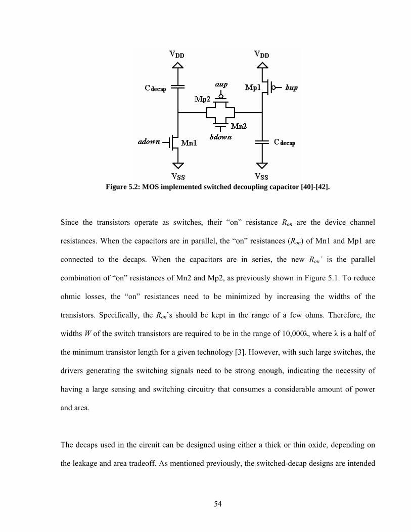
Figure 5.2: MOS implemented switched decoupling capacitor [40]-[42].
Since the transistors operate as switches, their “on” resistance Ron are the device channel
resistances. When the capacitors are in parallel, the “on” resistances (Ron) of Mn1 and Mp1 are
connected to the decaps. When the capacitors are in series, the new Ron’ is the parallel
combination of “on” resistances of Mn2 and Mp2, as previously shown in Figure 5.1. To reduce
ohmic losses, the “on” resistances need to be minimized by increasing the widths of the
transistors. Specifically, the Ron’s should be kept in the range of a few ohms. Therefore, the
widths W of the switch transistors are required to be in the range of 10,000λ, where λ is a half of
the minimum transistor length for a given technology [3]. However, with such large switches, the
drivers generating the switching signals need to be strong enough, indicating the necessity of
having a large sensing and switching circuitry that consumes a considerable amount of power
and area.
The decaps used in the circuit can be designed using either a thick or thin oxide, depending on
the leakage and area tradeoff. As mentioned previously, the switched-decap designs are intended
54

to maximize the area efficiency, and do not directly provide for any gate leakage savings.
However, some of the gate leakage saving techniques discussed in the previous chapters can be
applied here to control the leakage power.
5.3 Sun’s Voltage Regulator
Sun’s sensing and switching circuit is a voltage regulator (VR) that contains four main blocks: a
reference voltage generator, a high-pass filter, a two-stage amplifier, and switched decoupling
capacitors. The block diagram is illustrated in Figure 5.3 [41]. In the same figure, a user logic
circuit block is shown to be placed close to the active decap and is considered the main noise
source to the global power grid.
Figure 5.3: Block diagram of Sun voltage regulator [41].
55

Three modes of operation can be identified: standby, discharging, and charging. If a voltage
change ΔV on the power grid is sensed by the sensing circuitry, the voltage regulator will switch
from the standby state to the discharging state to boost the voltage level back up. After the
voltage difference at the power lines rises above the nominal value, the active decap will then
switch into the charging phase. When the power-grid voltages are back to the roughly nominal
values, the circuit changes to the standby mode. In the standby situation, both nodes bup and
adown are positioned at VDD/2, whereas aup is at roughly VDD and bdown is at roughly VSS. In
the discharging and charging phases, small input variations are amplified to a level where large
swings at the output are observed. The large swings of amplified signals are used to switch the
decoupling capacitors in either series or parallel.
Table 5.1 lists the node biasing and swing values [41]. Standby state indicates how the nodes are
biased in steady-state, while discharging and charging states specify the target voltage levels
under discharging or charging situations, respectively.
Table 5.1: Node biasing and swing for Sun voltage regulator [41].
aup adown bup bdown
Standby ~VDD VDD/2 VDD/2 ~VSS
Discharging ~VSS ~VSS ~VDD ~VDD
Charging ~VDD ~VDD ~VSS ~VSS
56
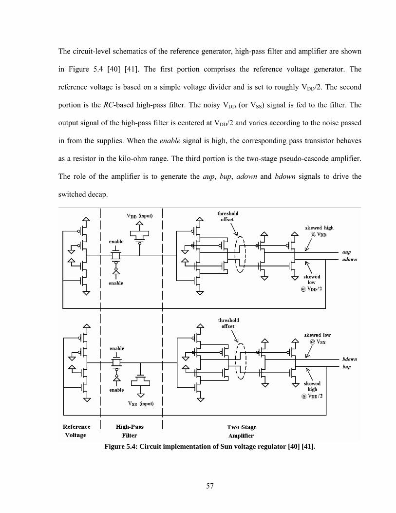
The circuit-level schematics of the reference generator, high-pass filter and amplifier are shown
in Figure 5.4 [40] [41]. The first portion comprises the reference voltage generator. The
reference voltage is based on a simple voltage divider and is set to roughly VDD/2. The second
portion is the RC-based high-pass filter. The noisy VDD (or VSS) signal is fed to the filter. The
output signal of the high-pass filter is centered at VDD/2 and varies according to the noise passed
in from the supplies. When the enable signal is high, the corresponding pass transistor behaves
as a resistor in the kilo-ohm range. The third portion is the two-stage pseudo-cascode amplifier.
The role of the amplifier is to generate the aup, bup, adown and bdown signals to drive the
switched decap.
Figure 5.4: Circuit implementation of Sun voltage regulator [40] [41].
57

To set the outputs at desired voltage levels at the amplifier stage of the circuit, proper sizing of
the transistors is required. Since the transistors in the first amplifier stage are on in standby, the
node voltages are determined by the series resistance of the stacked transistors. Similarly, the
second stage of the amplifier can be considered as a ratioed inverter. Thus, all the nodes that are
skewed either high or low by the second stage of the amplifier can approach VDD or VSS, but not
reach these values. Typically, the large swings at the aup, bup, adown and bdown signals will
result in longer delay (switching time), but will save standby power consumption. Overall, the
sizes of the transistors can be designed by considering the target voltage levels, the desired slew
rate at the output, and the total power budget.
The operation of the VR moves from standby to discharging to charging. The voltage regulator
configuration implies that the decoupling capacitors are in shunt in both standby and charging
states. The only situation that capacitors will be switched into series is when the power grid
discharges due to logic gates switching in the user logic circuit. From simulation results, this
shunt to series switch does not happen until the voltage variation exceeds a certain threshold, for
example 60mV. In other words, the sensitivity of the sensing circuitry in this VR that would
trigger a switch of the decaps from parallel to series is at about 60mV.
One interesting feature of the VR is the feedback loop. Both adown and bup are fed back to the
reference generator to enhance stability. Because these two nodes are biased at VDD/2, they
require the voltage levels at the internal nodes to stabilize after a few ripples generated by the
power grid noise. Intuitively, the gain of the amplifier stage must be large since there is a small
58

signal at the input and a large signal at the output. Such a high-gain system has the potential
problem of oscillation in the presence of small power grid noise. The feedback ensures that the
oscillation will not occur in the system.
The main drawback of the VR is its power consumption. The switch transistors as a part of the
switched decaps are normally large to produce small “on” resistances (Ron), as mentioned in the
previous section. To drive those large switches, however, it is required that the second stage of
the amplifier (ratioed inverter) is large enough. Since both adown and bup are biased at VDD/2 in
the standby state, both PMOS and NMOS transistors of the inverter are in saturation region,
resulting in relatively high standby power. The high power requirement for the Sun voltage
regulator limits its use to high-performance ICs only. For low power ASICs or even portable
devices, such a design cannot be used without modifications.
5.4 Fujitsu’s Active Power Stabilizer
Based on Sun’s voltage regulator, designers from Fujitsu developed an active power stabilizer
(APS), as shown in Figure 5.5, to help reduce power grid voltage fluctuations [42]. The switched
decaps are the same as before and are not included in the figure. Conceptually, the APS and the
VR are similar. The small-signal portions of the two designs are almost identical. The basic
structure includes a pair of switched decoupling capacitors, a reference generator, and a high-
pass filter. However, the two designs differ in the amplification stage.
59

Figure 5.5: Circuit implementation of Fujitsu active power stabilizer [42].
Similar to Sun’s VR, the reference generation is provided by a simple voltage divider without the
feedback characteristics. An identical high-pass filter is utilized to sense the VSS grid voltage
variations and pass the signal to the amplification stage. The noise on the VDD grid is assumed to
be a duplicate of the VSS grid noise and hence is not monitored. Unlike Sun’s VR, Fujitsu’s APS
uses two differential pairs with current mirrors to produce the first-stage amplification. Each
amplifier is capable of providing full swings at the output if the two input nodes are properly
biased [43]. However, the gain of such a stage is typically not large. The differential amplifier is
followed by a common-source amplifier with a current-source load. The required voltage drop
across the current-source load (or required VDS across the load transistor) degrades the maximum
voltage swing at the output, V+ and V- [43]. The third amplification stage is a chain of standard
CMOS inverters that provides two valuable features: (1) the capability of regenerating logic
values (either VDD or VSS) at the output by increasing the voltage swings, and (2) the capability
60

of driving large output loads without slew rate limitations. The inverter chain can be sized using
the procedure of logical effort [42].
In the APS circuit in Figure 5.5, the nodes at which the switches are turned on or off to drive the
decaps are biased differently from Sun’s VR in the standby state. Referring back to Figure 5.2,
the voltages for each node are listed in Table 5.2 [42]. It is evident that there is no equivalent
decoupling capacitance at all in the standby mode since all the switches (Mn1, Mn2, Mp1, and
Mp2) of the switched decap are turned off. The other modes remain the same as in the case of the
Sun VR.
Table 5.2: Node biasing and swing for Fujitsu active power stabilizer [42].
aup adown bup bdown
Standby VDD VSS VDD VSS
Discharging VSS VSS VDD VDD
Charging VDD VDD VSS VSS
Compared to Sun’s VR, Fujitsu’s APS has the following advantages. Knowing that the APS
occupies slightly less or comparable area compared to the VR, its power consumption is only
about 1% of the Sun VR (details in Section 5.6). Such low power characteristics make it
attractive for many ASIC designs. Also, it has better control on sensitivity. In the Fujitsu circuit
shown in Figure 5.5, the sensitivity was ideally set to be 15mV (per rail). In practice, the circuit
will switch only if more than 25mV of voltage variation is present in the power grid. This
61

triggering voltage can be easily adjusted by sizing the transistors differently in the reference
voltage generator.
On the other hand, the APS also experiences the disadvantages of longer delay time and the
potential problem of self-oscillation. The delay time occurs due to insertion of the CMOS
inverter chains. For a 0.13um simulation process, the delay can be 300ps or more. For the
purpose of regulating voltage variations, such a long delay is not appropriate since the
instantaneous voltage drop on the power grid requires an immediate circuit response to boost the
voltage back up. The switching response that happens after a long delay is not particularly useful.
The other problem is possible self-oscillation. Specifically, lacking a feedback loop, the presence
of a switching delay and high sensitivity level may cause oscillations if the gain of the first two
stages of the amplifier (the differential pair and the common-source amplifier) is inadvertently
large.
In addition, there are some minor disadvantages of the APS. If the power grid noise is less than
the sensitivity level of the APS, the circuit stays in the standby mode and both decaps are
disconnected from the power grid. This configuration is undesirable. Also, the two biasing
voltages, Vbias1 and Vbias2, need to be generated by additional reference circuitry. Although
not included in the figure, this reference circuitry requires additional area and power
consumption.
62

5.5 Low-Power Voltage Regulator
After investigating the voltage regulator and the active power stabilizer, it is clear that each one
has its own advantages and drawbacks. There still exists a need for developing a new design that
has better noise reduction performance than the APS but also requires much less power than the
VR. The motivation for the new design is to properly balance performance and power. More
specifically, the goal of the new circuit is to try to match the performance of the VR, while trying
to control the power dissipation similar to the APS.
To understand the new design, first consider Figure 5.2 again. Shown in Table 5.1, in standby
condition, both adown and bup are biased at roughly VDD/2 in Sun’s VR. To turn off the two
corresponding switches (Mn1 and Mp1), adown needs to be lowered to below VT and bup needs
to be raised to above VDD – VT. The delay is basically the average time it takes to shift the two
voltage levels, and this delay runs counter to the capability of rapid noise regulation.
The new circuit attempts to increase the voltage swing at adown and bup. That is, in the standby
mode, adown is biased roughly at VDD, whereas bup is set at about VSS. This reduces the dc
current of the amplifier. When switched from standby to discharging state, adown must now fall
from ~VDD to VT, while bup has to rise from ~VSS to VDD – VT. In order to have a large output
swing, a common-source amplifier with triode load is chosen to be the second stage of the
amplifier. In order to shorten the delay time for large signal transitions, large transistors in the
amplifier are necessary. The detailed node biasing and transition details are listed in Table 5.3.
63

Table 5.3: Node biasing and swing for low-power voltage regulator.
aup adown bup bdown
Standby ~VDD ~VDD ~VSS ~VSS
Discharging ~VSS ~VSS ~VDD ~VDD
Charging ~VDD ~VDD ~VSS ~VSS
The next step is to design the first amplification stage. Since the main purpose of the second
stage is to provide driving capability while the output swing is considered for low power, the
first stage needs to provide a high gain. One simple implementation is to use a push-pull
amplifier. The push-pull nature of a pseudo-inverter-like amplifier provides a high gain if biased
properly [44]. In addition, the push-pull amplifier also has a high output swing. Typically, a
cascode amplifier can provide higher gain due to its high output impedance [43]. Thus,
combining the cascode and the push-pull amplifier together, a pseudo-cascode amplifier is used
for the first amplification stage.
One concern of such a pseudo-cascode amplifier would be its limited input swing. However, the
input of the first-stage amplifier is fed from the high-pass filter and can only vary in the range of
100mV. If the reference generator is well-designed and biases the input of the amplifier at the
margin of its high-gain region, the limited input swing of the amplifier is not a problem. Another
concern for the amplifier would be variations in the gain under process and temperature
variations. In order to have the reference voltages track the high gain region, a reference
generator that has a similar structure to the pseudo-cascode amplifier is used.
64
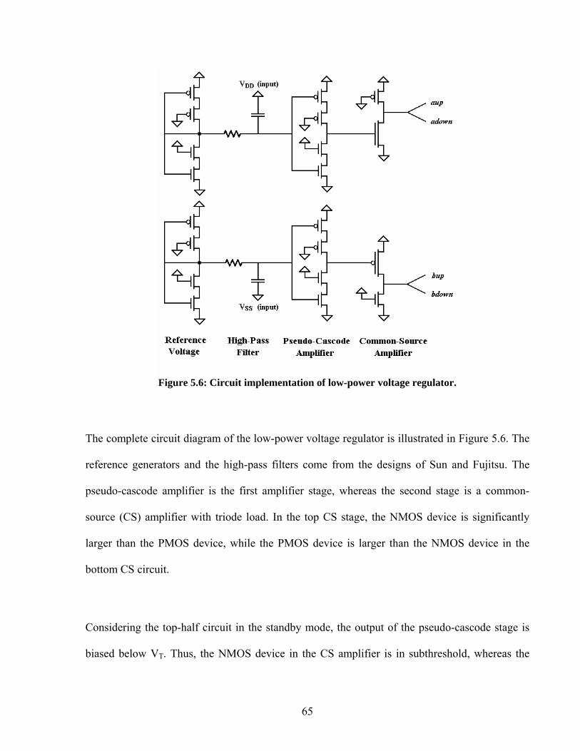
Figure 5.6: Circuit implementation of low-power voltage regulator.
The complete circuit diagram of the low-power voltage regulator is illustrated in Figure 5.6. The
reference generators and the high-pass filters come from the designs of Sun and Fujitsu. The
pseudo-cascode amplifier is the first amplifier stage, whereas the second stage is a common-
source (CS) amplifier with triode load. In the top CS stage, the NMOS device is significantly
larger than the PMOS device, while the PMOS device is larger than the NMOS device in the
bottom CS circuit.
Considering the top-half circuit in the standby mode, the output of the pseudo-cascode stage is
biased below VT. Thus, the NMOS device in the CS amplifier is in subthreshold, whereas the
65

PMOS device in the CS is in saturation. This results in the output nodes of the CS close to VDD.
When the power grid starts discharging, the output of the pseudo-cascode stage rises. Assuming
that the voltage drop in the power grid is ΔV and the gain of the pseudo-cascode amplifier is A,
the gate voltage at the NMOS device in the CS rises by AΔV, which will bring it into saturation
if the gain A is large enough. Once the NMOS device is in saturation, the PMOS device in the
CS will be forced into the linear (or triode) region. Since both transistors are on, the output is
ratioed and is fairly close to VDD because the size of the NMOS device is much larger than the
size of the PMOS device. All the above discussion applies in a complementary way to the
bottom-half circuit.
In the standby mode, the NMOS device in the top CS and the PMOS device in the bottom CS
experience a comparatively large amount of subthreshold leakage because their sizes are large.
This subthreshold leakage, however, is still much less than the on current in the last
amplification stage in Sun’s VR. Moreover, since the transistor sizes are large enough to provide
driving capability, the delay time for the low-power VR does not increase significantly compared
to Sun’s VR. Hence, the performance of regulating power grid noise is not reduced noticeably
for the new design. From simulation results, the power dissipation for the low-power VR is
approximately at 10% of the Sun VR. However, its power is still larger than the Fujitsu APS.
The new design removes the feedback connection since the standby voltage levels at the output
of the amplifier and at the reference generator are no longer identical. That is, in the standby
state, the output of the amplifier is at either ~VDD or ~VSS, whereas the reference voltage is set to
66

be roughly VDD/2 to bias the pseudo-cascode in its maximum gain region. Therefore, the output
signal cannot be fed back to the reference in this new design. Losing the feedback characteristics
reduces the stability of the circuit. If the gain of the pseudo-cascode is too large, the output nodes
will start oscillating. Designers need to size the amplifier properly to have a suitable gain to
avoid this potential problem. Or, if a longer delay is tolerable, the biasing voltage from the
reference generator can be shifted slightly away from the high gain region of the amplifier to
avoid oscillation.
5.6 Simulation Setup and Results
The simulations for all the designs were carried out using HSPICE under BSIM 3v2 transistor
models in a 0.13um technology. Since BSIM 3v2 does not support thin-oxide gate leakage
simulation, all the power calculations exclude the tunneling leakage, which makes the results
slightly optimistic. However, compared to the power dissipation level in the circuit designs, the
tunneling leakage is only a small portion of the total power. If thick-oxide decaps are used, the
gate leakage can be neglected. Although the simulations were carried out in a 0.13um process, it
can be easily adapted for a 90nm process or below since the design concept remains the same.
In realistic designs, two elements contribute to the voltage variation ΔV on the power grid:
power-grid resistance R and packaging inductance L. The simulation needs to consider both IR
drop and Ldi/dt effect. To estimate the power mesh resistance R, a Layer-8 metal-sheet resistance
is considered for a 0.13um, 8-layer copper process, assuming metals 7-8 have a thickness of
0.8um and a width of 20um. The sheet resistance Rsq is roughly 1.7uΩ-cm / 0.8um = 20mΩ/.
67
Suppose the mesh length is 100um, one can have the mesh resistance Rmesh equal to
20mΩ/ 100 )20
mmμ
(μ
= 0.1Ω.
The inductance L is due to packaging via and bumps (solder balls) from either dual-inline or ball-
grid-array (BGA) packaging method. A typical number for the packaging inductance from a
BGA packaging option is 0.2nH on both VDD and VSS lines [3]. This 0.2nH applies to all the
simulations for consistency.
The simulation setup is shown in Figure 5.7. The simplified user logic circuit consists of a
switching inverter and a load capacitance Cload connected at the output of the inverter. Since
only one inverter is used for simplicity, the size of the inverter is large with the PMOS device at
10,000λ / 2λ and the NMOS device at 5,000λ / 2λ. A pair of switched decoupling capacitors has
an equivalent capacitance value of 0.1nF with 0.05nF on each. The load capacitance Cload is set
to be 0.1nF since designers typically set Cdecap to be at least 2 to 10 times larger than the Cload
to keep the power grid noise within 10% noise budget [4]. A periodic ramp signal Vtest driving
the inverter gate comes from an ideal voltage source, and its switching frequency is set to be
400MHz, a typical value for modern ASICs.
68

Figure 5.7: Simulation setup for active decap circuits.
The decap circuit in the setup can be standard decaps, Sun VR, Fujitsu APS, or the low-power
VR. Initially, no decap circuit will be used as a reference point for the other circuits. It is
important to understand that this simulation setup is somewhat contrived. However, realistic
values of packaging inductance, power-mesh resistance and parasitic decoupling capacitance
have been used wherever possible.
The results are shown in Figures 5.8 to 5.12. The plots illustrate transient analyses for a time
interval of 15ns. The upper lines represent the voltage values at the global VDD, whereas the
lower lines are the voltage numbers at the global VSS. Quantitatively, the performance of the
designs can be determined by measuring the voltage variations on either of the noisy VDD or VSS
power line. A smaller voltage variation on the power grid indicates that the circuit has better
performance.
69

-0.2
0
0.2
0.4
0.6
0.8
1
1.2
1.4
0 2.5 5 7.5 10 12.5 15
Time (ns)
Vol
tage
(V)
Figure 5.8: Simulation results for no decap inserted.
-0.2
0
0.2
0.4
0.6
0.8
1
1.2
1.4
0 2.5 5 7.5 10 12.5 15
Time (ns)
Vol
tage
(V)
Figure 5.9: Simulation results for standard decaps inserted.
70

-0.2
0
0.2
0.4
0.6
0.8
1
1.2
1.4
0 2.5 5 7.5 10 12.5 15
Time (ns)
Vol
tage
(V)
Figure 5.10: Simulation results for Sun VR inserted.
-0.2
0
0.2
0.4
0.6
0.8
1
1.2
1.4
0 2.5 5 7.5 10 12.5 15
Time (ns)
Vol
tage
(V)
Figure 5.11: Simulation results for Fujitsu APS inserted.
71

-0.2
0
0.2
0.4
0.6
0.8
1
1.2
1.4
0 2.5 5 7.5 10 12.5 15
Time (ns)
Vol
tage
(V)
Figure 5.12: Simulation results for low-power VR inserted.
The simulation results of Figures 5.8 to 5.12 are consistent with the expected performance of the
circuits described in the earlier sections. The standard decap helps to reduce noise to a certain
extent, but the active decap designs provide better performance. From another perspective,
assuming the area is fixed, the active designs have better area/noise efficiency. However, the
noise reduction performance of each circuit improves at the expense of increasing power
consumption. A standard decoupling capacitor ideally consumes zero power if not considering
gate leakage, but its noise regulation performance is the lowest. Sun’s voltage regulator, on the
other hand, is the most effective design in terms of power-grid noise reduction, but it requires the
most dc power dissipation. Fujitsu’s active power stabilizer and the low-power voltage regulator
lie somewhere in between the two extremes.
72

The detailed dc power numbers are as follows: The Sun VR draws roughly 25mA of dc current
in standby, which corresponds to about 30mW of power for 0.13um technology. The Fujitsu
APS consumes 250uA of dc power, only about 1% of the Sun VR. The power dissipation for the
low-power VR is approximately 2.6mA (3.0mW), 90% less than the Sun VR.
The simulation uses a 400 MHz clock to switch a large buffer connected to the power grid.
Under this situation, the regulation performance between the low-power VR and Sun VR is
reasonably close. It is shown that for operating at a few hundred megahertz range, the low-power
version performs well in a 0.13um simulation process.
73

Chapter 6
Conclusions and Future Work
6.1 Summary
As technology scales further into the deep submicron regime, with increasing clock frequency
and decreasing supply voltage, maintaining the quality of power supply becomes a critical issue.
On-chip power supply noise, due to IR drop and Ldi/dt effects, has a great impact on delay
variation, and may even cause improper functionality. Power supply noise can be reduced by
placing decoupling capacitors close to power pads and large drivers throughout the power
distribution system. Decaps provide instantaneous current to the switching drivers and keep the
power supply within certain noise budgets.
Traditionally, a standard decap is made from an NMOS transistor outside the standard-cell
blocks, or a pair of NMOS and PMOS transistors within the blocks. However, starting from
90nm technology, the oxide thickness of MOS transistors is reduced to approximately 2.0nm or
less, resulting in increased ESD risk and gate leakage. Standard decap designs, therefore, may no
longer be appropriate for 90nm and below because they suffer greatly from these two problems.
74

In this thesis, the goal was to provide practical solutions to decap design for present-day and
upcoming technologies. The thesis began with an overview of decap modeling, gate leakage
phenomenon, ESD occurrence, and basic decap layout knowledge. Some essential decap design
issues were highlighted through the background discussion to motivate the topics in the rest of
the thesis.
Next, a number of design approaches for decaps in recent technologies were described along
with their advantages and disadvantages. The approaches from circuit level, including cross-
coupled decap, gated decap, and thick-oxide decaps were discussed first. The use of high-k gate
dielectrics and MIM capacitors were also described. In order to make further improvement from
the existing design approaches, the cross-coupled decap design was chosen because of its use in
existing libraries.
In the basic cross-coupled design, the tradeoff between ESD reliability and transient response is
a key issue. The objective was to achieve gate leakage savings while keeping a reasonable
tradeoff between ESD and transient response. This thesis proposed three modifications of the
basic cross-coupled design. Among the three, Mod2 is designed to replace the cross-coupled
design for reduced leakage; Mod1 has the best ESD performance; Mod3 provides better transient
response and the least gate leakage.
Finally, the designs of active decoupling capacitors for power-grid noise reduction were
investigated. The switched decaps amplify the charge storage capacity of the basic decap while
monitoring the power rail activity to provide dynamic control of the switching response. The
75

switched decaps have better area efficiency and better noise reduction performance than the
passive decaps. It was observed that the Sun Voltage Regulator (VR) performs well but
dissipates excessive power, whereas the Fujitsu Active Power Stabilizer (APS) saves power but
experiences excessively long delays. A new low-power switched-decap voltage regulator was
proposed to make design tradeoffs between power and performance. The low-power VR adopts
novel amplification circuitry to control its power consumption while providing a reasonable
swing at the output. Its noise reduction performance is acceptable and close to the Sun VR when
operated in moderate frequencies.
6.2 Contributions in this Thesis
The following summarizes the major contributions in this thesis: • Developed practical decap layouts that properly tradeoff between transient response
performance, ESD reliability, and gate leakage;
• Designed a low-power voltage regulator using switched decaps that provides adequate
power-noise reduction performance while consuming relatively low standby power.
6.3 Future Work
A number of issues regarding decoupling capacitors will have to be addressed in the near future.
First, knowing that the thin-oxide decaps leak a significant amount of current in 90nm and below,
it is important to place only the necessary amount of decaps in a certain design to avoid
overdesign. The use of thick-oxide decaps may not solve the issue completely because the
effective capacitance is much less for thick-oxide devices and the total free area for decaps is
limited. Also, the active decaps provide better noise reduction performance but at a cost of
76

increased standby power requirement, compared to the passive decaps. Therefore, to determine
the optimal number of thick-oxide, thin-oxide and active decaps to be placed into a design
remains a challenge.
Another issue would be the placement of decaps. The proper placement and use of active decaps
versus passive decaps is still under investigation. The presence of power-grid noise is indeed a
two-dimensional problem. The noise is related to logic block, clock tree and power mesh
distribution throughout the chip. Hence, the optimal placement of decaps must consider the
placement of other functional blocks. Moreover, for each empty area reserved for decap use, it is
questionable whether a thin-oxide cross-coupled decap, a thick-oxide standard decap, or a
voltage regulator should be placed.
So far, the decap performance is mainly evaluated through simulations. It would be important to
carry out post-fabrication tests to extract real measurement values. Monitoring power supply
fluctuations on-chip [45] [46] in real-time is also an emerging area of research and should be
pursued to operate in conjunction with voltage regulators.
77

REFERENCES
[1] N. Na; T. Budell, C. Chiu, E. Tremble, and I. Wemple, “The Effects of On-Chip and Package Decoupling Capacitors and an Efficient ASIC Decoupling Methodology,” Proceedings of Electronic Components and Technology (ECTC '04), Volume 1, pp. 556-567, June 2004.
[2] H. Su, S. S. Sapatnekar, and S. R. Nassif, “Optimal Decoupling Capacitor Sizing and Placement for Standard-Cell Layout Designs,” IEEE Transactions on Computer-Aided Design of Integrated Circuits and Systems, Volume 22, Issue 4, pp. 428-436, April 2003.
[3] D. A. Hodges, H. G. Jackson and R. A. Saleh, Analysis and Design of Digital Integrated Circuits in Deep Submicron Technology, 3rd Ed, McGraw-Hill, 2004.
[4] J. Chia, “Design, Layout and Placement of On-Chip Decoupling Capacitors in IP Blocks”, M.A.Sc Thesis, University of British Columbia, 2004.
[5] T. S. Horng, A. Tseng, H. H. Huang, S. M. Wu, and J. J. Lee, “Comparison of Advanced Measurement and Modeling Techniques for Electrical Characterization of Ball Grid Array Packages,” IEEE 48th Electronic Components and Technology Conference, pp. 1464-1471, May 1998.
[6] N. Srivastava, X. Qi, and K. Banerjee, “Impact of On-Chip Inductance on Power Distribution Network Design for Nanometer Scale Integrated Circuits,” Sixth International Symposium on Quality of Electronic Design (ISQED’05), pp. 346-351, March 2005.
[7] H. H. Chen and S. E. Schuster, “On-Chip Decoupling Capacitor Optimization for High-Performance VLSI Design”, in Proceeding of International Symposium on VLSI Technology, Systems, and Applications, 1995, pp. 99-103.
[8] J. Kim, B. Choi, H. Kim, W. Ryu, Y. -H. Yun, S. -H. Hamm, S. -H. Kim, and Y. -H. Lee, “Separated Role of On-Chip and On-PCB Decoupling Capacitors for Reduction of Radiated Emission on Printed Circuit Board,” IEEE International Symposium Electromagnetic Compatibility, Volume 1, pp. 531-536, Aug. 2001.
[9] H. H. Chen, J. S. Neely, M. F. Wang, and G. Co, “On-Chip Decoupling Capacitor Optimization for Noise and Leakage Reduction”, in Proceedings of Symposium on Integrated Circuits and Systems Design, 2003, pp. 319-326.
[10] A. Amerasekera and C. Duvvury, ESD in Silicon Integrated Circuits, 2nd Ed, John Wiley & Sons, 2002.
[11] TSMC 90nm CLN90G Process SAGE-X v3.0 Standard Cell Library Databook, Release 1.0, Artisan Components Inc., 2004.
78

[12] Y. Chen, H. Li, K. Roy, and C. -K. Koh, “Gated Decap: Gate Leakage Control of On-Chip Decoupling Capacitors in Scaled Technology,” IEEE Custom Integrated Circuits Conference, pp. 775-778, Sep. 2005.
[13] P. Larsson, “Parasitic Resistance in an MOS Transistor Used as On-Chip Decoupling Capacitance,” IEEE Journal of Solid-State Circuits, Volume 32, Issue 4, pp. 574-576, April 1997.
[14] W. Liu, “MOSFET Models for SPICE Simulation including BSIM3v3 and BSIM4,” John Wiley & Sons, Inc., 2001.
[15] K. Roy, S. Mukhopadhyay, and H. Mahmoodi-Meimand, “Leakage Current Mechanisms and Leakage Reduction Techniques in Deep-Submicrometer CMOS Circuits,” Proceedings of IEEE, Volume 91, Issue 2, pp. 305-327, Feb. 2003.
[16] W. C. Lee and C. Hu, “Modeling Gate and Substrate Currents due to Conduction- and Valence-Band Electron and Hole Tunneling,” in Digest of Technical Papers, Symposium on VLSI Technology, 2000, pp. 198-199.
[17] F. Hamzaoglu and M. Stan, “Circuit-Level Techniques to Control Gate Leakage for sub-100nm CMOS,” in Proceedings of International Symposium on Low Power Design, 2002, pp. 60–63.
[18] K. Cao, W. -C. Lee, W. Liu, X. Jin, P. Su, S. K. H. Fung, J. X. An, B. Yu, and C. Hu, “BSIM4 Gate Leakage Model including Source Drain Partition,” in Technical Digest, IEDM, 2000, pp. 815-818.
[19] X. Xi, M. Dunga, J. He, W. Liu, K. M. Cao, X. Jin, J. J. Ou, M. Chan, A. M. Niknejad, and C. Hu, “BSIM4.4.0 MOSFET Model User’s Manual,” University of California, Berkeley, 2004.
[20] R. S. Guindi and F. N. Najm, “Design Techniques for Gate-Leakage Reduction in CMOS Circuits,” in Proceedings of Fourth International Symposium on Quality Electronic Design, 2003, pp. 61-65.
[21] S. Zhao, K. Roy and C. -K. Koh, “Decoupling Capacitance Allocation and Its Application to Power-Supply Noise-Aware Floorplanning,” IEEE Transactions on Computer-Aided Design of Integrated Circuits and Systems, Volume 21, Issue 1, pp 81-92, Jan. 2002.
[22] J. Fu, Z. Luo, X. Hong, T. Cai, S. X. -D. Tan, and Z. Pan, “VLSI On-Chip Power/Ground Network Optimization Considering Decap Leakage Currents,” Proceedings of Asia and South Pacific Design Automation Conference, Volume 2, pp. 735-738, Jan. 2005.
[23] R. I. Bahar, and S. Manne, “Power and Energy Reduction via Pipeline Balancing,” Proceedings of 28th Annual International Symposium on Computer Architecture, 2001, pp. 218-229.
[24] PMC-Sierra Design Rule for Lambda 90nm, Issue 3, PMC-Sierra Inc., 2005.
79

[25] PMC-Sierra Design Rule for 0.13um Salicide Technology, Issue 11, PMC-Sierra Inc., 2003.
[26] X. W. Wang, Y. Shi, T. P. Ma, G. J. Cui, T. Tamagawa, J. W. Golz, B. L. Halpen, and J. J. Schmitt, “Extending Gate Dielectric Scaling Limit by Use of Nitride or Oxynitride,” International Symposium on VLSI Technology, pp. 109-110, June 1995.
[27] T. P. Ma, “Opportunities and Challenges for High-k Gate Dielectrics”, Proceedings of the 11th International Symposium on the Physical and Failure Analysis of Integrated Circuits (IPFA 2004), pp. 1-4, July 2004.
[28] C. W. Yang, Y. K. Fang, C. H. Chen, W. D. Wang, T. Y. Lin, M. F. Wang, T. H. Hou, J. Y. Cheng, L. G. Yao, S. C. Chen, C. H. Yu, and M. S. Liang, “Dramatic Reduction of Gate Leakage Current in 1.61 nm HfO2 High-k Dielectric Poly-Silicon Gate with Al2O3 Capping Layer,” Electronics Letters, Volume 38, Issue 20, pp. 1223-1225, Sep. 2002.
[29] T. P. Ma, “Electrical Characterization of High-k Gate Dielectrics,” Proceedings on 7th International Conference on Solid-State and Integrated Circuits Technology, Volume 1, pp. 361-365, Oct. 2004.
[30] P. Vitanov, A. Harizanova, and T. Ivanova, “Thin Metal Films for Application in Nanoscale Devices,” 27th International Spring Seminar on Electronics Technology: Meeting the Challenges of Electronics Technology Progress, Volume 2, pp. 252-256, May 2004.
[31] D. Lee, W. Kwong, D. Blaauw, and D. Sylvester, “Analysis and Minimization Techniques for Total Leakage Considering Gate Oxide Leakage,” Proceedings of 40th DAC, pp 175-180, June 2003.
[32] M. Armacost, A. Augustin, P. Felsner, Y. Feng, G. Friese, J. Heidenreich, G. Hueckel, O. Prigge, and K. Stein, “A High Reliability Metal Insulator Metal Capacitor for 0.18 um Copper Technology,” IEDM Technical Digest, pp. 157-160, Dec. 2000.
[33] M. W. C. Goh, Q. Lim, R. A. Keating, A. V. Kordesch, and Y. Bin Mohd Yusof, “Design of Radio Frequency Metal-Insulator-Metal (MIM) Capacitors,” Proceedings of 7th International Conference on Solid-State and Integrated Circuits Technology, Volume 1, pp. 209-212, Oct. 2004.
[34] C. H. Ng, C. S. Ho, N. G. Toledo, and S. -F. Chu, “Characterization and Comparison of Single and Stacked MIMC in Copper Interconnect Process for Mixed-Mode and RF Applications,” IEEE Electron Device Letters, Volume 25, Issue 7, pp. 489-491, July 2004.
[35] C. H. Ng, C. S. Ho, S. -F. S. Chu, and S. -C. Sun, “MIM Capacitor Integration for Mixed-Signal/RF Applications,” IEEE Transactions on Electron Devices, Volume 52, Issue 7, pp. 1399-1409, July 2005.
[36] L. Chang, K. J. Yang, Y. -C. Yeo, Y. -K. Choi, T. -J. King, and C. Hu, “Reduction of Direct-Tunneling Gate Leakage Current in Double-Gate and Ultra-Thin Body MOSFETs,” IEDM Technical Digest, pp. 5.2.1-5.2.4, Dec. 2001.
80

[37] X. Meng, K. Arabi, and R. Saleh, “Novel Decoupling Capacitor Designs for sub- 90nm CMOS Technology”, accepted at IEEE International Symposium on Quality Electronic Design, March 2006.
[38] R. Saleh, J. Chia, X. Meng, and K. Arabi, “Modeling and Design of Standard Cell Decoupling Capacitors for sub- 100nm CMOS Technology”, submitted to IEEE Transactions on Computer-Aided Design of Integrated Circuits and Systems, Dec. 2005.
[39] C. K. Alexander and M. N. O. Sadiku, Fundamentals of Electric Circuits, McGraw-Hill, 2000.
[40] M. Ang, R. Salem, and A. Tayloy, “An On-chip Voltage Regulator Using Switched Decoupling Capacitors,” IEEE International Solid-State Circuits Conference, pp. 438-439, Feb. 2000.
[41] M. A. Ang, and A. D. Tayloy, “Voltage Regulating Circuit for Attenuating Inductance-Induced On-Chip Supply Variations,” U.S. Patent 6,028,471, 2000.
[42] C. Giacomotto, R. P. Masleid, and A. Harada, “Four-state Switched decoupling Capacitor System for Active Power Stabilizer,” U.S. Patent 6,744,242 B1., 2004.
[43] B. Razavi, Design of Analog CMOS Integrated Circuits, McGraw Hill, 2001.
[44] R. J. Baker, CMOS: Circuit Design, Layout, and Simulation, 2nd Ed., IEEE Press, 2005.
[45] E. Alon, V. Stojanovic, and M. A. Horowitz, “Circuits and Techniques for High-Resolution Measurement of On-Chip Power Supply Noise”, IEEE Journal of Solid-State Circuits, Volume 40, Issue 4, pp. 820-828, April 2005.
[46] T. Nakura, M. Ikeda, and K. Asada, “Design and Measurement of On-Chip di/dt Detector Circuit for Power Supply Line”, Proceedings of 2004 IEEE Asia-Pacific Conference on Advanced System Integrated Circuits, pp. 426-427, Aug. 2004.
81