decoder-based circuits - howard huanghowardhuang.us/teaching/cs231/05-decoder-based-circuits.pdf ·...
TRANSCRIPT

June 24, 2003 ©2000-2003 Howard Huang 1
Decoder-based circuits
Today we’ll study decoders, another commonly-used circuit.This lecture will follow the outline of yesterday’s multiplexer lecture.— There are different ways to design and build decoders.— Decoders can be used to implement arbitrary functions.— As always, we depend upon Boolean algebra to analyze circuits.
We’ll also talk ROMs and PLAs, programmable circuits based on decoders.

June 24, 2003 Decoder-based circuits 2
Multiplexer review
A 2n-to-1 multiplexer routes one of 2n input lines to a single output line.A block diagram, truth table and Boolean expression for a 4-to-1 muxwith an active-low enable input are given below.
Notice that the n select inputs allow us to choose one of 2n data inputs.
1xx1
D3110D2010D1100D0000
QS0S1EN’
Q = S1’S0’D0 + S1’S0 D1 + S1 S0’D2 + S1 S0 D3
June 24, 2003 Decoder-based circuits 3
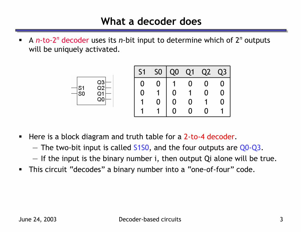
What a decoder does
A n-to-2n decoder uses its n-bit input to determine which of 2n outputs will be uniquely activated.
Here is a block diagram and truth table for a 2-to-4 decoder.— The two-bit input is called S1S0, and the four outputs are Q0-Q3.— If the input is the binary number i, then output Qi alone will be true.
This circuit “decodes” a binary number into a “one-of-four” code.
100011010001001010000100
Q3Q2Q1Q0S0S1

June 24, 2003 Decoder-based circuits 4
Building a decoder
We can use the truth table to derive minimal sum of products equations for each of the four outputs (Q0-Q3), based on the two inputs (S0-S1).
In this case there’s not much to be simplified. Here are the equations:
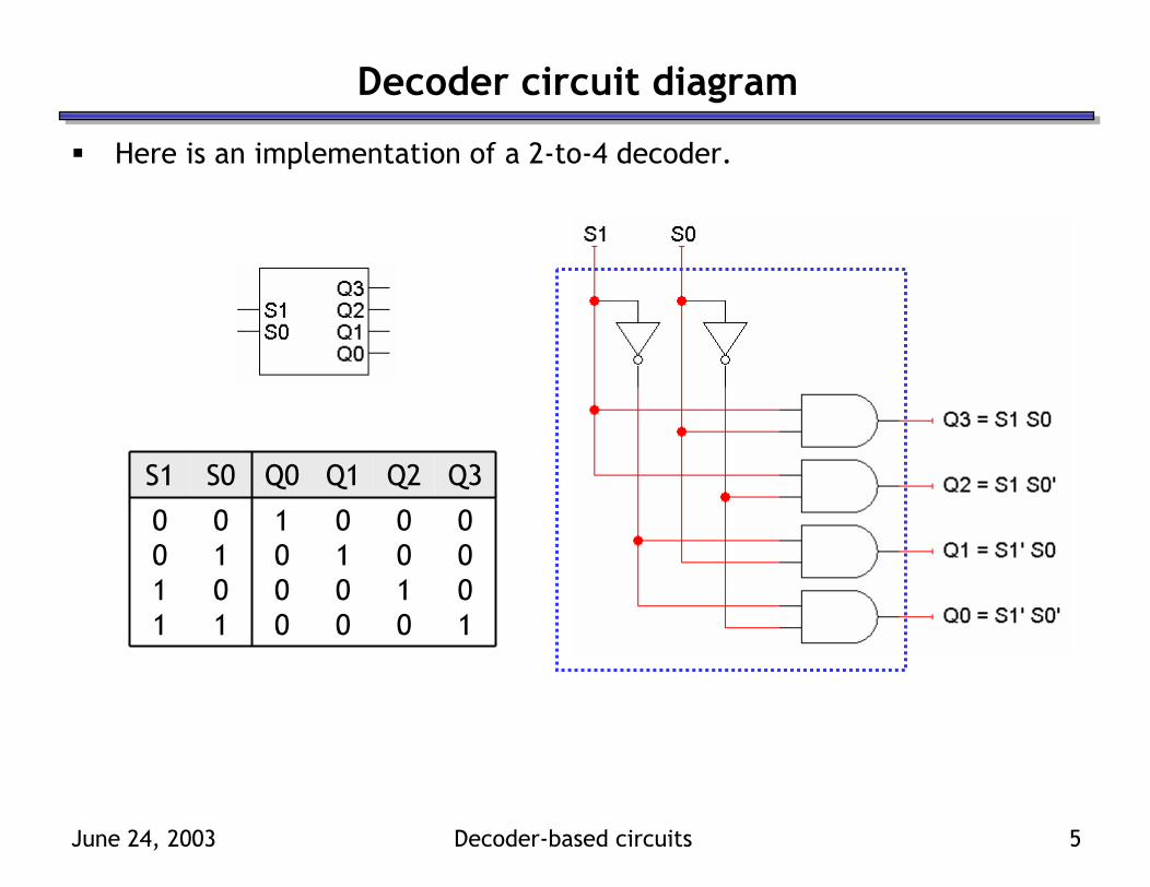
Q0 = S1’S0’Q1 = S1’S0Q2 = S1 S0’Q3 = S1 S0
100011010001001010000100
Q3Q2Q1Q0S0S1
June 24, 2003 Decoder-based circuits 5
Decoder circuit diagram
Here is an implementation of a 2-to-4 decoder.
100011010001001010000100
Q3Q2Q1Q0S0S1

June 24, 2003 Decoder-based circuits 6
Multiplexers and decoders
Here is the implementation of the 4-to-1 multiplexer from last time.
This mux includes a 2-to-4 decoder internally! Multiplexers are really just a (very useful) application of decoders.

June 24, 2003 Decoder-based circuits 7
Enable inputs
Just as with multiplexers, decoders can include enable inputs.— EN=0 disables the decoder, which by convention means that all of the
decoder’s outputs are 0.— EN=1 enables the decoder so that it behaves as specified earlier, with
exactly one of the outputs being 1.
0000xx0
1111
EN
100011010001001010000100
Q3Q2Q1Q0S0S1
June 24, 2003 Decoder-based circuits 8
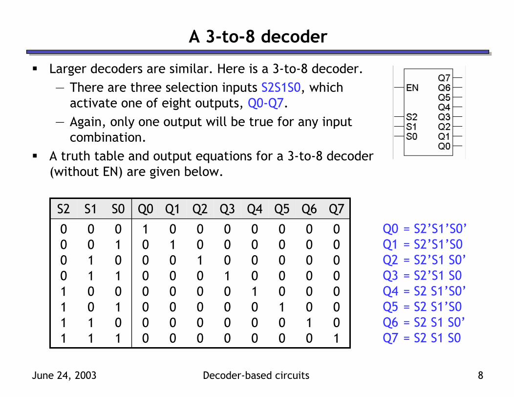
A 3-to-8 decoder
Larger decoders are similar. Here is a 3-to-8 decoder.— There are three selection inputs S2S1S0, which
activate one of eight outputs, Q0-Q7.— Again, only one output will be true for any input
combination.A truth table and output equations for a 3-to-8 decoder (without EN) are given below.
1000000011101000000011001000001010001000000100001000110000001000100000001010000000001000
Q7Q6Q5Q4Q3Q2Q1Q0S0S1S2
Q0 = S2’S1’S0’Q1 = S2’S1’S0Q2 = S2’S1 S0’Q3 = S2’S1 S0Q4 = S2 S1’S0’Q5 = S2 S1’S0Q6 = S2 S1 S0’Q7 = S2 S1 S0

June 24, 2003 Decoder-based circuits 9
Building a 3-to-8 decoder
You could build a 3-to-8 decoder from the truth table and MSP equations below, just like we built the 2-to-4 decoder earlier.Another way to design a decoder is to break it into smaller pieces. Notice some patterns in the table below:— When S2 = 0, outputs Q0-Q3 are generated as in a 2-to-4 decoder.— When S2 = 1, outputs Q4-Q7 are generated as in a 2-to-4 decoder.
1000000011101000000011001000001010001000000100001000110000001000100000001010000000001000
Q7Q6Q5Q4Q3Q2Q1Q0S0S1S2

June 24, 2003 Decoder-based circuits 10
Decoder expansion
Here’s a 3-to-8 decoder built from two smaller 2-to-4 decoders.When S2=0, the bottom 2-to-4 decoder is enabled and generates a 1 for one of outputs Q0, Q1, Q2 or Q3.When S2=1, the top 2-to-4 decoder is enabled instead, and a 1 will be output for either Q4, Q5, Q6 or Q7.
1000000011101000000011001000001010001000000100001000110000001000100000001010000000001000
Q7Q6Q5Q4Q3Q2Q1Q0S0S1S2

June 24, 2003 Decoder-based circuits 11
Modularity
You could verify that this circuit is a 3-to-8 decoder, by using equations for the 2-to-4 decoders to derive equations for the 3-to-8.Be careful not to confuse the “inner” inputs and outputs of the 2-to-4 decoders with the “outer” inputs and outputs of the 3-to-8 decoder.This is similar to having several functions in a program which all use a formal parameter “x”.
June 24, 2003 Decoder-based circuits 12
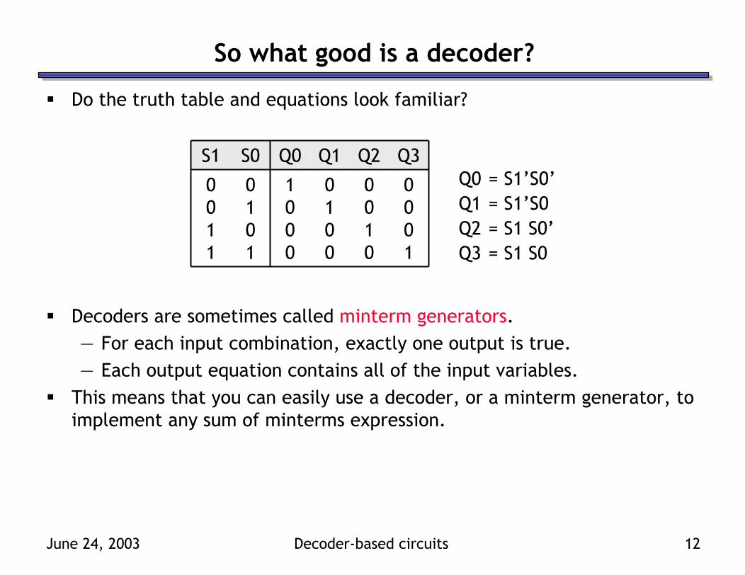
So what good is a decoder?
Do the truth table and equations look familiar?
Decoders are sometimes called minterm generators.— For each input combination, exactly one output is true.— Each output equation contains all of the input variables.
This means that you can easily use a decoder, or a minterm generator, to implement any sum of minterms expression.
100011010001001010000100
Q3Q2Q1Q0S0S1Q0 = S1’S0’Q1 = S1’S0Q2 = S1 S0’Q3 = S1 S0

June 24, 2003 Decoder-based circuits 13
Example: addition
Yesterday we presented a simple circuit which added three 1-bit inputs X, Y and Z to produce a two-bit output, C (“carry”) and S (“sum”).A truth table and sum of minterm equations for C and S are shown below.
Today we’ll implement these two functions using 3-to-8 decoders.
11101000
C
11110011010110010110101011000000
SZYX
C(X,Y,Z) = Σm(3,5,6,7)S(X,Y,Z) = Σm(1,2,4,7)

June 24, 2003 Decoder-based circuits 14
Implementing functions with decoders
Here, a 3-to-8 decoder implements C as a sum of minterms.
If XYZ is 011, 101, 110 or 111, then one of the decoder outputs Q3, Q5, Q6 or Q7 will be true, and the output C(X,Y,Z) will also be true.The “+5V” symbol (“5 volts”) represents a 1 or true in LogicWorks.

June 24, 2003 Decoder-based circuits 15
Verifying our adder
C is the sum of decoder outputs Q3, Q5, Q6 and Q7.
C = Q3 + Q5 + Q6 + Q7
We know how the decoder’s outputs are generated from its inputs.
C = S2’S1S0 + S2S1’S0 + S2S1S0’ + S2S1S0
We can substitute XYZ for S2S1S0, resulting in a sum of minterms that matches the one we started with on page 13.
C = X’YZ + XY’Z + XYZ’ + XYZ
June 24, 2003 Decoder-based circuits 16
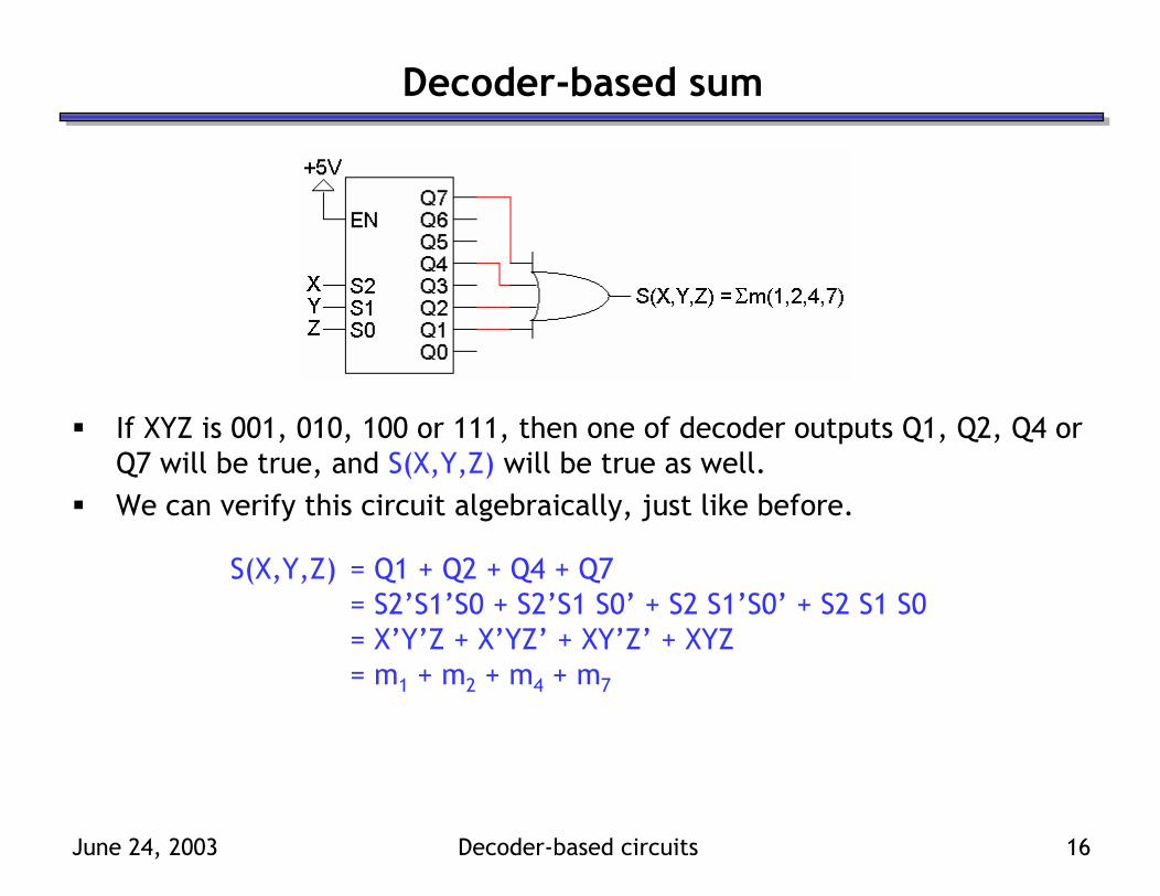
Decoder-based sum
If XYZ is 001, 010, 100 or 111, then one of decoder outputs Q1, Q2, Q4 or Q7 will be true, and S(X,Y,Z) will be true as well.We can verify this circuit algebraically, just like before.
S(X,Y,Z) = Q1 + Q2 + Q4 + Q7= S2’S1’S0 + S2’S1 S0’ + S2 S1’S0’ + S2 S1 S0= X’Y’Z + X’YZ’ + XY’Z’ + XYZ= m1 + m2 + m4 + m7

June 24, 2003 Decoder-based circuits 17
Using just one decoder
Since the two functions C and S both have the same inputs, we could use just one decoder instead of two.
Decoder output Q0 is unused, while Q7 is used multiple times. In general, you can always use circuit outputs as many or as few times as you need.

June 24, 2003 Decoder-based circuits 18
A variation of the standard decoder
The decoders we’ve seen so far are active-high decoders.
An active-low decoder is similar, but with an inverted EN input andinverted outputs—exactly one of the outputs will be false.
1000111010001100101010001001
0000xx0
Q3Q2Q1Q0S0S1EN
1111xx1
0111110101101011011001110000
Q3’Q2’Q1’Q0’S0S1EN’

June 24, 2003 Decoder-based circuits 19
Separated at birth?
Active-high decoders generate minterms, as we’ve already seen.
Q3 = S1 S0Q2 = S1 S0’Q1 = S1’S0Q0 = S1’S0’
The output equations for an active-low decoder are mysteriously similar, yet somehow different.
Q3’ = (S1 S0)’ = S1’+ S0’Q2’ = (S1 S0’)’ = S1’+ S0Q1’ = (S1’S0)’ = S1 + S0’Q0’ = (S1’S0’)’ = S1 + S0
It turns out that active-low decoders generate maxterms, so they can implement functions as sums of maxterms.
June 24, 2003 Decoder-based circuits 20
Active-low decoder example
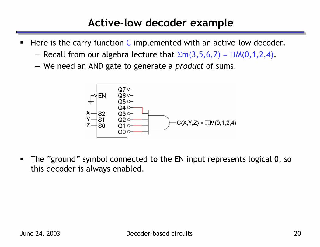
Here is the carry function C implemented with an active-low decoder.— Recall from our algebra lecture that Σm(3,5,6,7) = ΠM(0,1,2,4).— We need an AND gate to generate a product of sums.
The “ground” symbol connected to the EN input represents logical 0, so this decoder is always enabled.
June 24, 2003 Decoder-based circuits 21
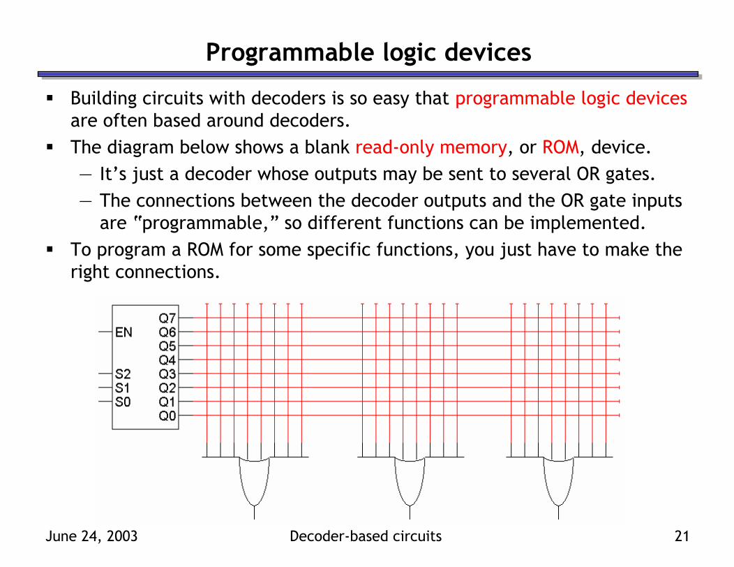
Programmable logic devices
Building circuits with decoders is so easy that programmable logic devicesare often based around decoders.The diagram below shows a blank read-only memory, or ROM, device.— It’s just a decoder whose outputs may be sent to several OR gates.— The connections between the decoder outputs and the OR gate inputs
are “programmable,” so different functions can be implemented.To program a ROM for some specific functions, you just have to make the right connections.

June 24, 2003 Decoder-based circuits 22
ROM example
Here are three functions V2, V1 and V0, implemented with our ROM.Blue crosses (X) indicate connections between decoder outputs and OR gates. Empty intersections are not connected.This is an 8 × 3 ROM since there are 8 decoder outputs and 3 OR gates.
V2 = Σm(1,2,3,4) V1 = Σm(2,6,7) V0 = Σm(4,6,7)

June 24, 2003 Decoder-based circuits 23
The same example again
Here is an alternative presentation of the same 8 × 3 ROM, but with some simplified OR gates just to make the diagram neater.
V2 = Σm(1,2,3,4)V1 = Σm(2,6,7)V0 = Σm(4,6,7)

June 24, 2003 Decoder-based circuits 24
Why is this called a memory?
You can think of this circuit as performing a computation on the inputs A2A1A0, to produce the outputs V2V1V0.Note that if the same inputs are chosen again, this circuit would perform the same calculation again, and produce the same output.In a sense, the circuit “remembers” the output for each possible input.
110111110011000101101001001110011010001100000000
V0V1V2A0A1A2

June 24, 2003 Decoder-based circuits 25
Viewing circuits as memories
So you can also think of this circuit as a memory.— It stores eight values of data, each consisting of three bits V2V1V0.— A2A1A0 form an address that refers to one of the eight stored values.
This memory is read-only since you can’t modify the data without going through the time-consuming process of re-programming the ROM.
110111110011000101101001001110011010001100000000
V0V1V2A0A1A2DataAddress
June 24, 2003 Decoder-based circuits 26
Programmable logic arrays
A ROM is potentially inefficient since it uses a decoder, which generates all possible minterms. No circuit minimization is done.Using a ROM to implement an n-input function requires many gates.— An n-to-2n decoder has n inverters and 2n n-input AND gates.— We also need an OR gate with up to 2n inputs.— The number of gates roughly doubles for each additional ROM input.
A programmable logic array or PLA makes the decoder part of the ROM programmable too. Instead of generating all possible minterms, you can choose which products (not necessarily minterms) to generate.

June 24, 2003 Decoder-based circuits 27
A blank 3 × 4 × 3 PLA
This is a 3 × 4 × 3 PLA (3 inputs, up to 4 product terms, and 3 outputs), ready to be programmed.The left part of this diagram replaces the decoder used in a ROM.Connections are made within the AND array to produce four arbitrary products.Those products are then summed in the OR array.
Inputs
Outputs
AND array
OR array
June 24, 2003 Decoder-based circuits 28
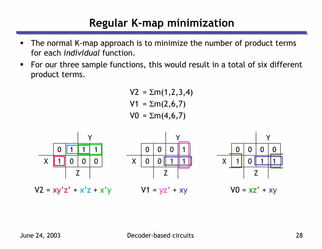
Regular K-map minimization
The normal K-map approach is to minimize the number of product terms for each individual function.For our three sample functions, this would result in a total of six different product terms.
V2 = Σm(1,2,3,4)V1 = Σm(2,6,7)V0 = Σm(4,6,7)
Z
0001X
1110
Y
Z
1100X
1000
Y
Z
1101X
0000
Y
V2 = xy’z’ + x’z + x’y V1 = yz’ + xy V0 = xz’ + xy
June 24, 2003 Decoder-based circuits 29
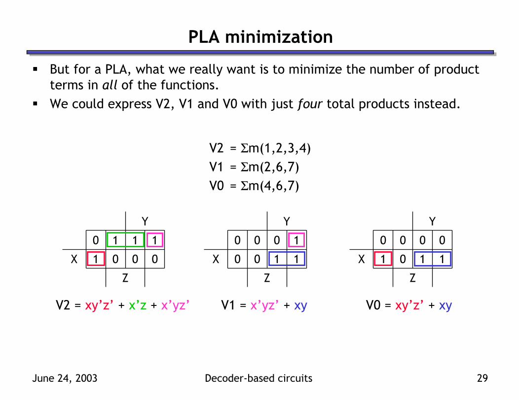
PLA minimization
But for a PLA, what we really want is to minimize the number of product terms in all of the functions.We could express V2, V1 and V0 with just four total products instead.
V2 = Σm(1,2,3,4)V1 = Σm(2,6,7)V0 = Σm(4,6,7)
Z
0001X
1110
Y
Z
1100X
1000
Y
Z
1101X
0000
Y
V2 = xy’z’ + x’z + x’yz’ V1 = x’yz’ + xy V0 = xy’z’ + xy

June 24, 2003 Decoder-based circuits 30
PLA example
So we can implement these three functions using a 3 × 4 × 3 PLA.
xy’z’
xy
x’z
x’yz’
V2 = Σm(1,2,3,4) = xy’z’ + x’z + x’yz’V1 = Σm(2,6,7) = x’yz’ + xyV0 = Σm(4,6,7) = xy’z’ + xy

June 24, 2003 Decoder-based circuits 31
PLA evaluation
A k × m × n PLA can implement as many as n functions of k inputs, each of which must be expressible with no more than m product terms.Unlike ROMs, PLAs allow you to choose which products are generated.— This can significantly reduce the fan-in (number of inputs) of gates, as
well as the total number of gates.— However, a PLA is less general than a ROM. Not every function may be
expressible with the limited number of AND gates in a given PLA.You can think of PLAs as memories too. — A k × m × n PLA has k “address” lines, and each of those 2k addresses
references an n-bit data value.— But again, not all possible data values can be stored.

June 24, 2003 Decoder-based circuits 32
Summary
An n-to-2n decoder uses its n-bit input to determine which of 2n outputs is uniquely true.— An n-to-2n decoder generates the minterms of an n-variable function,
so decoders can be used to implement arbitrary functions.— Basic decoder variants include enable inputs and active-low decoders,
which can implement product of maxterms expressions. Like muxes, decoders illustrate our circuit analysis and design methods.— We can implement decoders from an initial problem specification.— Boolean algebra helps us verify the correctness of our designs.
Programmable devices are two more ways to implement circuits.— ROMs are simpler to program, but may contain extra gates.— PLAs use less hardware, but require some minimization effort. Also,
the AND array size can limit the number of expressible functions.ROMs and PLAs may be considered as memories. Each input corresponds to an address, and the output is the data stored at that address.