datapath architecture for reliable...
TRANSCRIPT
DATAPATH ARCHITECTURE FOR RELIABLE COMPUTING IN NANO-SCALE
TECHNOLOGY
A thesis work submitted to the faculty of
San Francisco State University
In partial fulfillment of
The requirements for
The Degree
Masters in Science
In
Engineering: Embedded Electrical and Computer Systems
by
Harsh Vakhariya
San Francisco, California.
January 2012

Copyrights by
Harsh Vakhariya
2012
CERTIFICATION OF APPROVAL
I certify that I have read Datapath Architecture for Reliable Computing in Nanoscale
Technology by Harsh Vakhariya, and that in my opinion his work meets the criteria for
approving a thesis submitted in partial fulfillment of the requirement for the degree:
Master of Science in Engineering as San Francisco State University.
________________________________________________
Hamid Mahmoodi
Assistant Professor, Electrical and Computer Engineering
________________________________________________
Hamid Shahnaser
Professor, Electrical and Computer Engineering
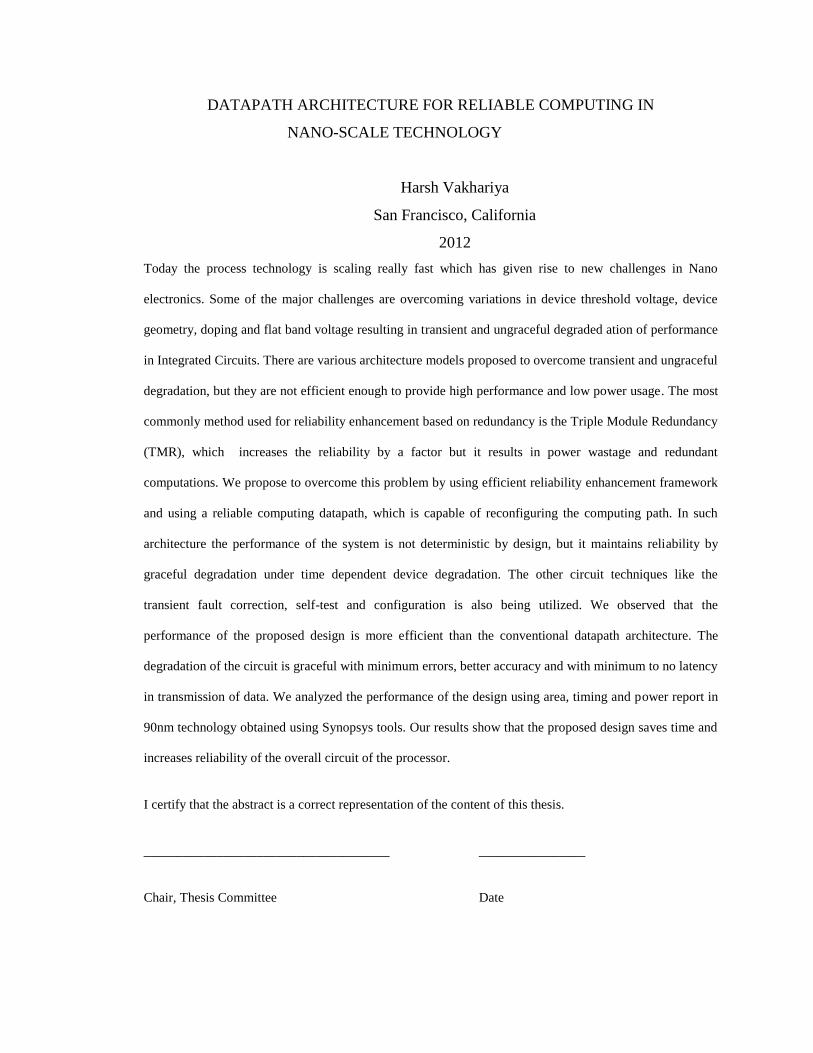
DATAPATH ARCHITECTURE FOR RELIABLE COMPUTING IN
NANO-SCALE TECHNOLOGY
Harsh Vakhariya
San Francisco, California
2012
Today the process technology is scaling really fast which has given rise to new challenges in Nano
electronics. Some of the major challenges are overcoming variations in device threshold voltage, device
geometry, doping and flat band voltage resulting in transient and ungraceful degraded ation of performance
in Integrated Circuits. There are various architecture models proposed to overcome transient and ungraceful
degradation, but they are not efficient enough to provide high performance and low power usage. The most
commonly method used for reliability enhancement based on redundancy is the Triple Module Redundancy
(TMR), which increases the reliability by a factor but it results in power wastage and redundant
computations. We propose to overcome this problem by using efficient reliability enhancement framework
and using a reliable computing datapath, which is capable of reconfiguring the computing path. In such
architecture the performance of the system is not deterministic by design, but it maintains reliability by
graceful degradation under time dependent device degradation. The other circuit techniques like the
transient fault correction, self-test and configuration is also being utilized. We observed that the
performance of the proposed design is more efficient than the conventional datapath architecture. The
degradation of the circuit is graceful with minimum errors, better accuracy and with minimum to no latency
in transmission of data. We analyzed the performance of the design using area, timing and power report in
90nm technology obtained using Synopsys tools. Our results show that the proposed design saves time and
increases reliability of the overall circuit of the processor.
I certify that the abstract is a correct representation of the content of this thesis.
_____________________________________ ________________
Chair, Thesis Committee Date

v
ACKNOWLEDGEMENTS
I would like to thank my thesis advisor Dr. Hamid Mahmoodi for his
invaluable guidance and support towards the completion of my thesis. I
would also like to thanks to my committee member Dr. Hamid Shahnasser
for his timely support and feedbacks. I am also thankful to the school of
engineering for providing me with the resources required for completing my
research. I would like to acknowledge Synopsys inc. for providing all the
hardware and EDA tools. Finally, I would like to thank the whole team of
NeCRL (Nano-electronics Computing and Research Laboratory) for their
support and resources.
vi
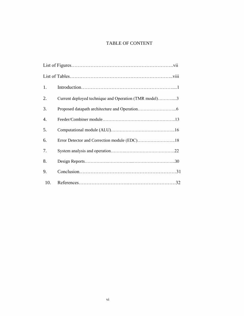
TABLE OF CONTENT
List of Figures……………………………………………………….vii
List of Tables………………………………………………………..viii
1. Introduction…………………………………………………....1
2. Current deployed technique and Operation (TMR model)……….....3
3. Proposed datapath architecture and Operation……………………...6
4. Feeder/Combiner module…………………………………………..13
5. Computational module (ALU)……………………………………..16
6. Error Detector and Correction module (EDC)……………………..18
7. System analysis and operation……….…………………………….22
8. Design Reports…………….……………...………………………..30
9. Conclusion………………………….…………………………31
10. References………………………….…………………………32

vii
LIST OF FIGURES
Fig.1 : Triple Modular Redundancy (TMR) scheme…………………………4
Fig.2: Initial system design with multiplexers and demultiplexers…………..7
Fig.3 : Improvised system architecture with feeder, combiner, error
detection & correction and built in self-test and configuration
modules…………………………………………………………………….…9
Fig.4 : Proposed system architecture with integrated
feeder/combiner, error detection and correction modules……………..……12
Fig.5 : Feeder/combiner module with input and output signals……………..15
Fig.6 : Computational module with its input/output signals…………….......17
Fig. 7: EDC block diagram………………………………………………….18
Fig.8 : Error Detection and Correction module……………………………..19
Fig.9 : C-element gate level design…………………………………………19
Fig. 10: C-element transistor design………………………………………...20
Fig.11 : Datapath architecture of the proposed design……………………...24
Fig.12 : Fault free computational modules………………………………….27
Fig.13 : One faulty computational module………………………………….28
Fig.14 : Two faulty computational modules…………………………….…..29

viii
LIST OF TABLES
Table 1: System states and corresponding error signals raised
by the Error Detection and Correction module…………………………….14
Table 2: Computational module operations………………………………..16
Table 3: C-element truth table……………………………………………..21
Table 4: Computation module reconfiguration…………………………….23
Table 5: Design reports…………………………………………………….30
1
1.Introduction
Over the last decade the size of semiconductors transistors has been rapidly
reducing. This rapid scaling of semiconductor in nanoscale has given rise to variety
of reliability issues. Although the size of chip has reduced significantly, modern day
processor architectures are yet to overcome these reliability issues, they are still not
efficient enough to balance reliability and performance while maintaining power.
There is a immense need to modify traditional microelectronics approaches to cope
with the emerging challenges in nanoscale technology. Device degradation due to
aging is one of the great concerns. The degradation factors are Negative Biased
Temperature Instability (NBTI), Positive Biased Temperature Instability (PBTI) and
Time Dependent Dielectric Breakdown (TDDB). These are all process related
factors resulting in device degradation, which result in faulty components and
modules on a larger picture, affecting the reliability and performance of the
architecture. The current designs employed to improve reliability do not take into
consideration the faulty components and their reconfiguration while considering
device aging. Considering data-path reconfiguration to bypass faulty components
and modules in the architecture along with the aging, results in reliable results and
high performance of the overall system. The main purpose of my research is to
develop an efficient technique to enhance reliability of digital designs in nanoscale
technology while maintaining its performance. As a result we developed a novel
redundancy and reconfigurability framework that is applicable to the innovative
circuit and micro-architecture co-design. The architecture designs proposed earlier

2
resulted in improvement of reliability up to a certain extent along with increasing its
power and area. This called for new techniques to be developed, which resulted in
our proposed architecture design. We developed a formal co-design methodology,
which is used for finding the best balance between resources and cost allocation of
circuit and micro-architectural level reliability parameters. For unreliability caused
by catastrophic device failures, we apply the resources at the micro-architectural
level to enhance system reliability.
3
2.Current deployed technique and Operation (TMR model)
The current technique used to enhance unreliability problem is based on
redundancy. Its called Triple Redundancy Model (TMR). Existing reliability
enhancement techniques based on redundancy are very costly in terms of area and
power dissipation. The basic idea behind this technique is to carry out redundant
computation with help of three identical models and use a voting circuit to get
reliable output. This mitigation uses three identical logic circuits (modules) to
perform essentially the same task in parallel. The corresponding outputs are then
compared with the help of majority voting circuit. This technique results in
improved reliability but it also results in increased power consumption. For the
classical TMR system, the reliability R (probability of correct computation) is given
by the expression stated below:
R = Rv (Rm + 3Rm2 (1-Rm )) = Rv (3Rm
2 - 2Rm
3 )
Where, Rm and Rv are the reliability (probability of correct computation) of each
individual module and the voter circuit, respectively. The TMR circuit is based on a
hypothesis that atleast two of the modules produce correct results out of the three,
Which would result in reliable computation by the system [1]. If two or more
modules become faulty the system will still produce results which are erroneous and
compromise reliability of the overall system. With each module becoming faulty
the performance of the overall system reduces. The throughput (f), power
dissipation (P) and area (A) of the existing system can modeled as:

4
f = fm
P = 3 X Pm + Pv
A = 3 X Am +Av
where, fm, Pm and Am are throughput, power and area of each module. Pv and Av are
power and area of the voter circuit.
As each modules carry out computations irrespective of their age or reliability and
their results are taken as input for the voter circuit; the area and power of the TMR
system is increased three times without any improvement in performance [2].
Output
In
Fig.1 shows Triple Modular Redundancy (TMR)
Computation
al Module1
Computation
al Module2
Computation
al Module3
Voter

5
In TMR the extra modules perform redundant computations that increase over all
power dissipation without improving the performance of the system.

6
3.Proposed Datapath Architecture and its Operation.
The proposed datapath architecture emphasizes on improving performance of the
system while making it more reliable. It includes combining parallelism and
pipelining to take advantage of both. Basic efficient reliability enhancement
framework incorporates testing of the faulty modules and non-faulty modules.
According to test results the system reconfigures itself to the best operating path;
resulting in high performance and reliability. Proposed architecture consists of a
feeder module with two 8-bit data input; which are fed to the processing modules.
The MSB of outputs from each module is fed to the Error Detection and Correction
module which tests for faulty modules and if the module is not faulty the output
from each module is propagated to the combiner module, which provides the final
output values. By reconfiguring the system we propose to reduce the redundant
computations and as a result, power.
The approach we chose to design the architecture was to go one block at a time.
First we implemented the basic multi ALU design. Two demultiplexers in a round
robin fashion provide the input to the ALU modules. Each ALU gets a set of input
data from the ALU, which is then processed and provided as input to the 3:1
multiplexer.

7
Fig.2 first step for the design.
8
There is a select signal to each ALU module, which decides the arithmetic, or
logical computation it is going to carry out. This design is useful for maximum
performance if all the components in the design are not faulty.
The above design was then improvised where the multiplexing and demultiplexing
operations were embedded into modules of combiner and feeder respectively. In
order to identify the faulty ALU an Error Detection and correction (EDC) module
was added in-between ALUs and the combiner module [3]. A testing module
identifies faulty and non-faulty modules and with the help of this information the
system reconfigures itself to yield optimum high performance operation. The feeder
module distributes the incoming data to the computing modules (ALU). The
combiner module collects the data from the three computing modules and sends the
result to the final system output. The error detection and correction module is based
on time shifted output technique. We have adapted this technique due to its low
overhead and soft error correction capability.
The output from the test signals and combiner module determine which of the
computational modules are error free and the faulty ones. Based on these data the
feeder module decides which computational modules are to be provided with inputs
and which are to be isolated and put to sleep. For example if module 2 is faulty, the
feeder will isolate the module 2 and provide inputs to module 1 and module 3; if
module 3 is faulty, feeder will isolate module 3 and provide inputs to module 1 and

9
module 2 and so on. This boost the performance of the system by a factor as
compared to TMR scheme. Figure 3 :

10
While designing the above proposed we came across few new ideas, which helped
us to reduce the number of modules in the system, resulting in decrease in area and
critical path of the system. This gave rise to our best-proposed architecture for
reliable computing for nanoscale technology.
11
Final datapath Architecture:
In the new improved architecture we combined the feeder and combiner module
together with the built in self test and reconfiguration module. The self-test and
reconfiguration operations are performed during run time to achieve reliability in
case of time dependent failure and/or aging effects. With the help of proposed
architecture the performance of the system and the reliability over time is
maintained. This system results in graceful degradation over the device aging effect
and maintains the functional reliability. The new architecture is as shown in the
figure below.
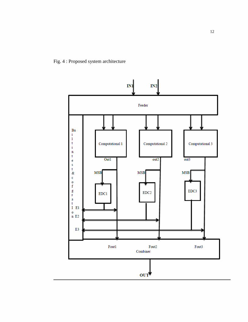
12
Fig. 4 : Proposed system architecture

13
4.Feeder / Combiner module:
The feeder combiner module is the module in the system architecture, which
provides 8 bit inputs to the computational modules. It also combines the outputs
from the computational modules and the Error Detection and Correction module
which are used to provide the system output. This module also takes error signals as
inputs which helps us configure and reconfigure the datapath depending on faulty or
non faulty modules. The 8 bit input from this module is provided as 8 bit inputs to
the computational modules in round robin fashion depending upon their error
signals. If the error signal is low (0) then the input is provided to the computational
and if the error signal is high (1) then the corresponding computational module is
isolated and not provided with any further input signal. The combiner part of this
module combines the output of each non-faulty computational modules and
provides with one final output. The output frequency is maintained constant
irrespective of the number of faulty modules in the system. The feeder combiner
module is the in-out module for the overall system architecture.
The input and output of this module is designed using state machines. The error
signals decide the state of the system executes and also it controls the inputs to the
computational modules and the outputs from which are to be propagated to the
combiner module. The number of states system executes depends on the error
signals raised by faulty computational modules. The basic logic used for designing
of feeder/combiner module can be explained using the table shown below.

14
State E1 E2 E3 Out
01 0 0 0 Fout1
10 0 0 0 Fout2
00 0 0 0 Fout3
01 0 0 1 Fout1
00 0 0 1 Fout2
01 0 1 0 Fout1
00 0 1 0 Fout3
01 1 0 0 Fout2
00 1 0 0 Fout3
00 0 1 1 Fout1
00 1 0 1 Fout2
00 1 1 0 Fout3
Table 1:states and corresponding error signals.
The above table explains the states the system goes through in case of
corresponding faulty module or modules.

15
Fig. 5 : feeder/combiner module

16
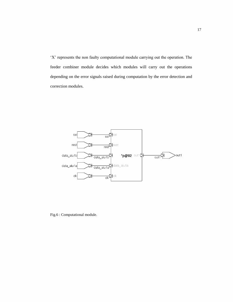
5. Computational module:
The computational module is the processing unit of the system. Which carries out
operation decided by the select signals on the inputs provided at the inputs. Each
has 2 eight bits input and 16 bits outputs. It basically carries out arithmetic and
logical operations. The computational module designed for the given system has
seven operations; four logical and three arithmetic. The table below shows the
operations and its corresponding select signals provided to the modules:
Select
signal
Operation Computation
000 + Addition data_aluXa + data_aluXb
001 | OR data_aluXa | data_aluXb
010 - Subtraction Data_aluXa – data_aluXb
011 & AND Data_aluXa & data_aluXb
100 ^ XOR Data_aluXa ^ data_aluXb
101 ~^ XNOR Data_aluXa ~^ data_aluXb
110 * Multiply Data_aluXa * data_aluXb
Table 2 :Computational module operations
17
„X‟ represents the non faulty computational module carrying out the operation. The
feeder combiner module decides which modules will carry out the operations
depending on the error signals raised during computation by the error detection and
correction modules.
Fig.6 : Computational module.
18
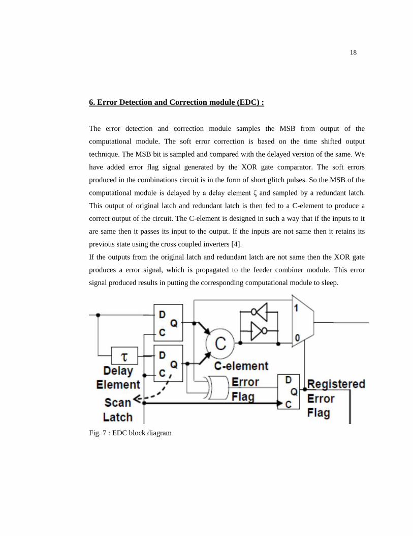
6. Error Detection and Correction module (EDC) :
The error detection and correction module samples the MSB from output of the
computational module. The soft error correction is based on the time shifted output
technique. The MSB bit is sampled and compared with the delayed version of the same. We
have added error flag signal generated by the XOR gate comparator. The soft errors
produced in the combinations circuit is in the form of short glitch pulses. So the MSB of the
computational module is delayed by a delay element ζ and sampled by a redundant latch.
This output of original latch and redundant latch is then fed to a C-element to produce a
correct output of the circuit. The C-element is designed in such a way that if the inputs to it
are same then it passes its input to the output. If the inputs are not same then it retains its
previous state using the cross coupled inverters [4].
If the outputs from the original latch and redundant latch are not same then the XOR gate
produces a error signal, which is propagated to the feeder combiner module. This error
signal produced results in putting the corresponding computational module to sleep.
Fig. 7 : EDC block diagram
19
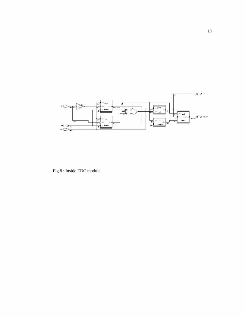
Fig.8 : Inside EDC module
20
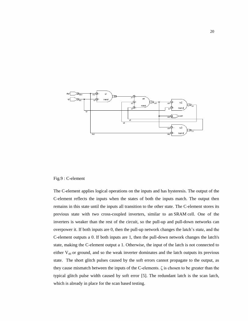
Fig.9 : C-element
The C-element applies logical operations on the inputs and has hysteresis. The output of the
C-element reflects the inputs when the states of both the inputs match. The output then
remains in this state until the inputs all transition to the other state. The C-element stores its
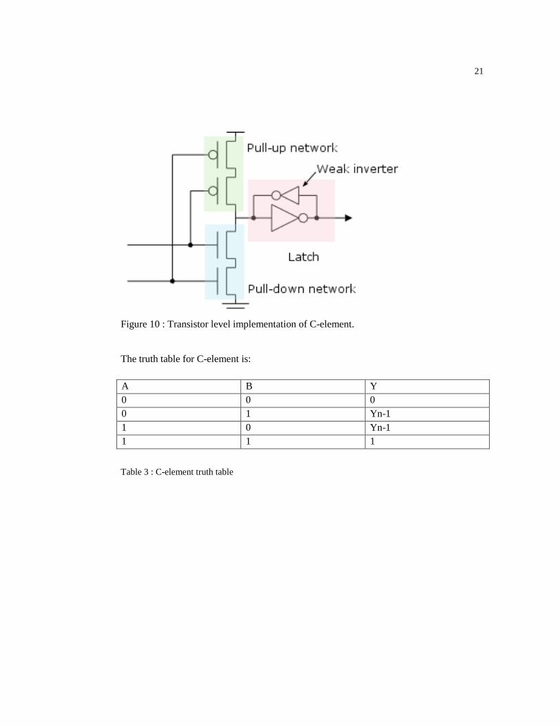
previous state with two cross-coupled inverters, similar to an SRAM cell. One of the
inverters is weaker than the rest of the circuit, so the pull-up and pull-down networks can
overpower it. If both inputs are 0, then the pull-up network changes the latch‟s state, and the
C-element outputs a 0. If both inputs are 1, then the pull-down network changes the latch's
state, making the C-element output a 1. Otherwise, the input of the latch is not connected to
either Vdd or ground, and so the weak inverter dominates and the latch outputs its previous
state. The short glitch pulses caused by the soft errors cannot propagate to the output, as
they cause mismatch between the inputs of the C-elements. ζ is chosen to be greater than the
typical glitch pulse width caused by soft error [5]. The redundant latch is the scan latch,
which is already in place for the scan based testing.
21
Figure 10 : Transistor level implementation of C-element.
The truth table for C-element is:
A B Y
0 0 0
0 1 Yn-1
1 0 Yn-1
1 1 1
Table 3 : C-element truth table

22
7. System analysis and validation:
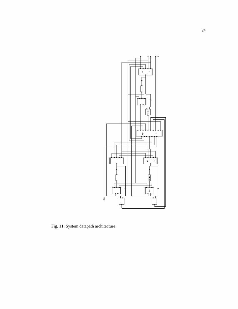
The System Architecture, when put together looks like the figure shown below. The
feeder combiner works as the input and the output of the system, as well as the built
in self-testing module. The computational modules carry out the arithmetic and
logical functions, whose outputs are 16bits. The MSB of the computational module
is fed to the error detection and correction module, which act as fault monitors on
each of them and registered as error flags. For multi output modules these delay
fault monitors will be inserted only at the outputs of the critical paths of each
module. The advantage of our scheme is that it will correct for both soft errors and
delay faults, thus simplifying dynamic reconfiguration design. The logic behind
employing fault monitors at critical paths of each module is that most aging and
catastrophic faults first manifest as delay faults. And upon occurrence of a delay
fault, the corresponding error flag will be raised and the system identifies the
computational module responsible for it. Once the faulty module is identified, the
system is reconfigured and only the non-faulty computational modules are provided
with input signals there on.
The system is provided with a frequency say F Hz. The speed of operation
is altered depending on number of fault free computational modules in the system
architecture. The frequency of the output data is maintained constant irrespective of
the faulty modules, thus maintaining the performance of the system. We have
introduced the signals delay1, delay2 and delay3 in order to induce errors in the
system to test it for error detection in the system.
The table shows the frequency reconfiguration in case of faulty computational
modules.
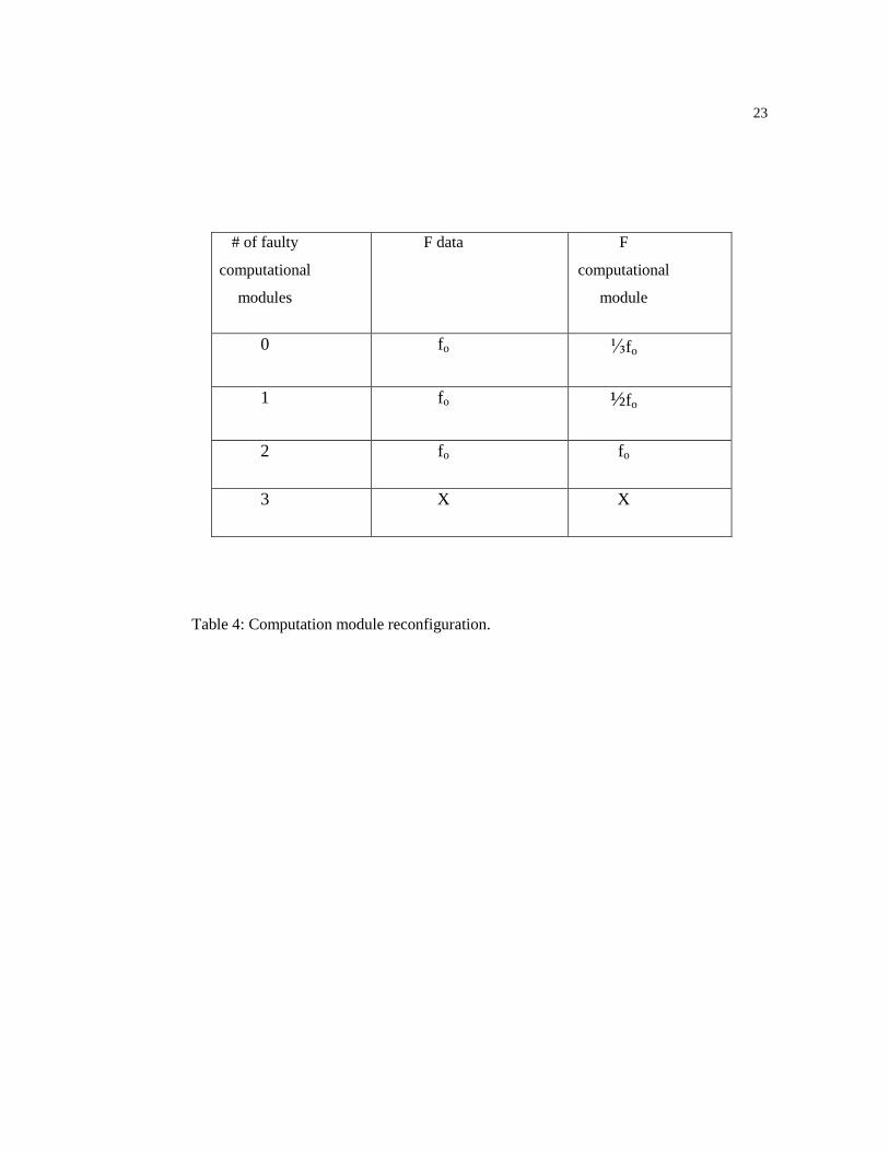
23
Table 4: Computation module reconfiguration.
# of faulty
computational
modules
F data F
computational
module
0 fo ⅓fo
1 fo ½fo
2 fo fo
3 X X
24
Fig. 11: System datapath architecture
25
System adaptation to faulty modules:
When all the three computational modules are fault free, each operates at a
frequency 1/3F Hz, as no error flags are raised. The 8-bit data input is provided in
round robin fashion and it carries out the computation based on the input provided
to the select signal. The output data frequency is same as the input data frequency.
In order to get no error in the first case we have not introduced any delay to the
delay1, delay2 and delay3 signals and provided them directly with MSB of each
computational module.
We can observe in the Figure 10 that two 8-bits inputs are given to the
feeder/combiner module, which in turn are fed to the computational modules in
round robin fashion. The input frequency of the data fed to each module is 1/3 of
input frequency. The MSB of the each computational output is fed to the error
detection and correction module. As delay applied to the MSB in the redundant
latch is under tolerable value, no error flags are raised, i.e E1, E2 & E3 are „0‟. The
output from each module is taken at the main output at frequency F Hz, same as
input frequency. The MSB is compared against its delayed version as explained in
the EDC module description.
Figure 11 shows Computational module 3 gone faulty. We have induced a delay of
4 ns along with the redundant latch delay ζ. This delay makes the input to C-
element different so it retains its previous, also the xor gate get two different inputs
which sets the error signal E3 high. As soon as the E3 goes high „1‟; the feeder
module stops feeding input to computational module 3. As a result the system
reconfigures itself with two modules working. The frequency of these two non-
faulty modules becomes ½ times the input frequency. The frequency of the final
output signal remains constant at F Hz.
Figure 12 shows two of the computational modules gone faulty. We induce
additional delay along with the ζ. This delay is too large, which results in different

26
inputs to the inputs of XOR gate which triggers the error flags. Also input to the C-
element results in it retaining the previous state. Once the error flags E2 and E3 are
raised the feeder does not feed inputs to the corresponding modules. The system
automatically reconfigures to input frequency and maintaining the output frequency.
Thus self-reconfiguration by the system upon error flag being raised results in
consistent performance. It reduces redundant computation unlike Triple Modular
Redundancy scheme.

27
Figure 12: Fault free computational modules.
E1 = E2 = E3 = 0
Each computational module frequency = 1/3F Hz.
28
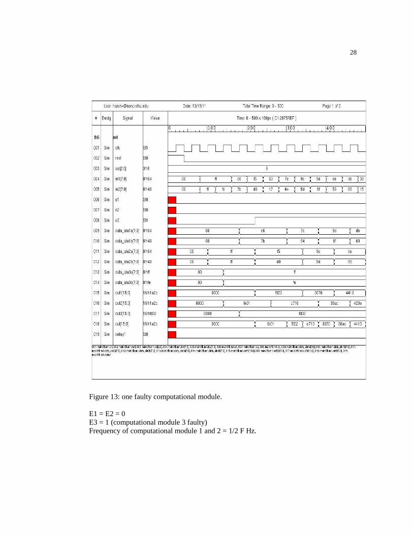
Figure 13: one faulty computational module.
E1 = E2 = 0
E3 = 1 (computational module 3 faulty)
Frequency of computational module 1 and 2 = 1/2 F Hz.

29
Figure 14: two faulty computational modules (2&3)
E1 = 0
E2 = E3 = 1
Frequency of computational module 1 = F Hz.

30
8.Design Report:
Number of non-
faulty
computational
modules
Area Power Timing
3 Combinational
Area:
17701.703153
Noncombinational
Area: 3215.432934
Cell Area:
20917.136086
Design Area:
20917.136086
Cell Internal Power
= 193.5800 uW
(87%)
Net Switching
Power = 29.1378
uW (13%)
Total Dynamic
Power = 222.7177
uW (100%)
Cell Leakage Power
= 77.0355 uW
Critical Path Clk
Period: 6.00
Resource Sharing:
1.00
Logic Optimization:
2.51
Mapping
Optimization:
12.70
Overall Compile
Time: 17.48
2 Combinational
Area:
19123.891169
Noncombinational
Area: 3215.432934
Cell Area:
22339.324103
Design Area:
22339.324103
Cell Internal Power
= 194.5057 uW
(86%)
Net Switching
Power = 31.2061
uW (14%)
Total Dynamic
Power = 225.7118
uW (100%)
Cell Leakage Power
= 81.5751 uW
Critical Path Clk
Period: 6.00
Resource Sharing:
0.24
Logic Optimization:
6.17
Mapping
Optimization:
8.31
Overall Compile
Time: 15.97
1 Combinational
Area:
17701.703153
Noncombinational
Area: 3215.432934
Cell Area:
20917.136086
Design Area:
20917.136086
Cell Internal Power
= 193.5800 uW
(87%)
Net Switching
Power = 29.1378
uW (13%)
Total Dynamic
Power = 222.7177
uW (100%)
Cell Leakage Power
= 77.0355 uW
Critical Path Clk
Period: 6.00
Resource Sharing:
1.02
Logic Optimization:
2.51
Mapping
Optimization:
12.71
Overall Compile
Time: 17.50
31
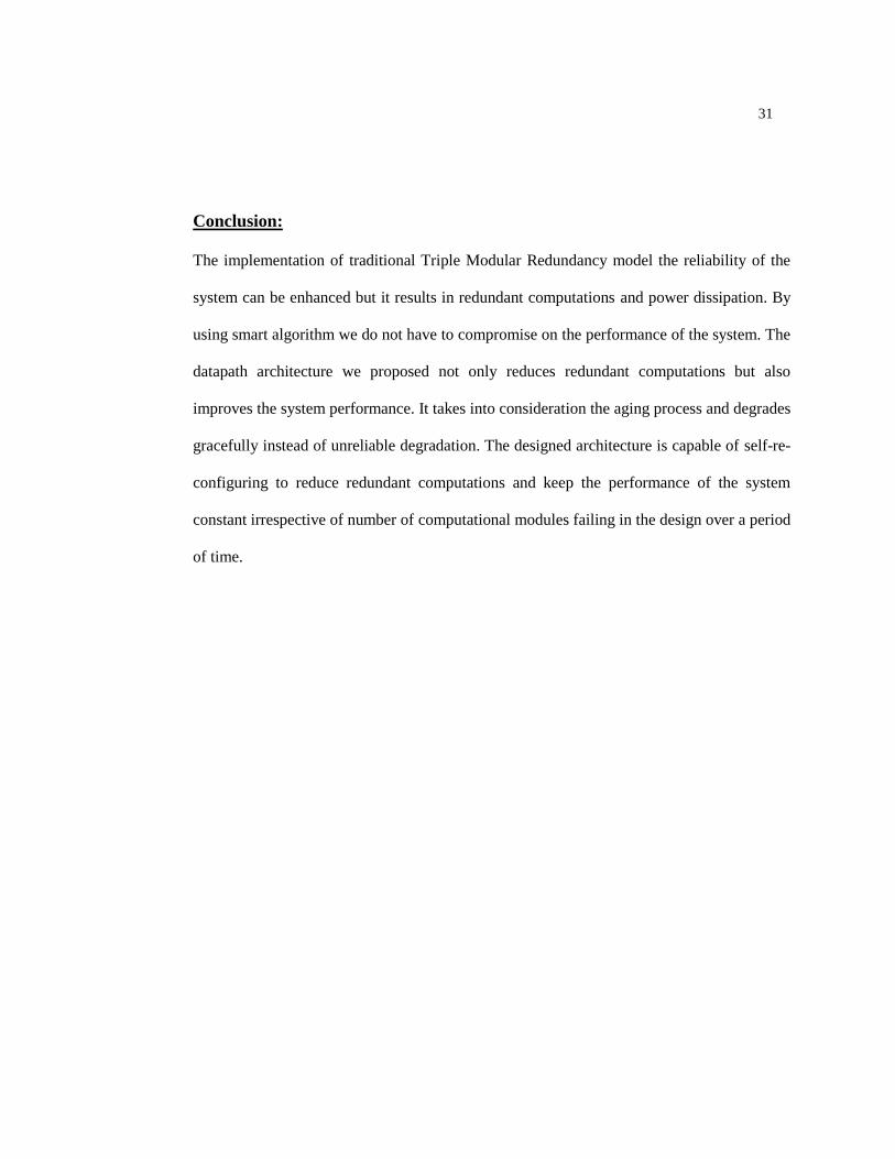
Conclusion:
The implementation of traditional Triple Modular Redundancy model the reliability of the
system can be enhanced but it results in redundant computations and power dissipation. By
using smart algorithm we do not have to compromise on the performance of the system. The
datapath architecture we proposed not only reduces redundant computations but also
improves the system performance. It takes into consideration the aging process and degrades
gracefully instead of unreliable degradation. The designed architecture is capable of self-re-
configuring to reduce redundant computations and keep the performance of the system
constant irrespective of number of computational modules failing in the design over a period
of time.

32
References:
1. Katsuyoshi Matsumoto et. Al., “Stateful tmr for transient faults.” World
automation congress, sep. 2010.
2. K.G.Shin et. Al., “A time redundancy approach to TMR failures using fault-
state likelihoods.” IEEE transaction on computers, issue -10, 1994. Pp 1151-1161.
3. S.N.Hamilton et. Al., “Self recovering controller and datapath codesign”,
Design, Automation and Test in Europe Conference and Exhibition 1999.pp 596-
601.
4. Subhasish Mitra et. Al., “Soft error resilient system design through error
correction.” IEEE 2007. Very Large Scale Integration, 2006 IFIP International
Conference. pp332-337.
5. Shuanguan Ruan et. Al., “Soft Error Hardened FF Capable of Detecting
Wide Error Pulse.” Defect and Fault Tolerance of VLSI Systems, 2008. DFTVS '08
International Symposium.pp272-280
6. Matteo Monchiero et. Al., “Power, Performance, Thermal sign space
exploration for multicore architectures.” IEEE may 2008.
7. Incorporating Effects of Process, Voltage and Temperature Variation in BTI model
for circuit design – Shreyas Kumar Krishnappa, Harwinder Singh and Dr. Hamid Mahmoodi
8. Digital Integrated Circuits – Jan Rabey
9. Advanced Digital Design with the Verilog HDL – Michael D. Cileeti
33
10. Verilog Digital System Design – Zainalabedin Navabi
11. Designing Digital Computer Systems with Verilog – David J. Lilja
12. Verilog digital computer design : algorithms into hardware - Mark Gordon