data sheet - electroniccircuits.gr · printed-circuits with high population densities. in these...
TRANSCRIPT

DATA SHEET
Preliminary specificationFile under Integrated Circuits, IC22
May 1993
INTEGRATED CIRCUITS
SAA7186Digital video scaler
May 1993 2
Philips Semiconductors Preliminary specification
Digital video scaler SAA7186
CONTENTS
1 FEATURES
2 GENERAL DESCRIPTION
3 QUICK REFERENCE DATA
4 ORDERING INFORMATION
5 BLOCK DIAGRAM
6 PINNING
7 FUNCTIONAL DESCRIPTION
8 OPERATION CYCLE
9 I2C-BUS FORMAT
10 LIMITING VALUES
11 DC CHARACTERISTICS
12 AC CHARACTERISTICS
13 PROCESSING DELAYS
14 PROGRAMMING EXAMPLE
15 PACKAGE OUTLINE
16 SOLDERING
17 DEFINITIONS
18 LIFE SUPPORT APPLICATIONS
19 PURCHASE OF PHILIPS I2C COMPONENTS
May 1993 3
Philips Semiconductors Preliminary specification
Digital video scaler SAA7186
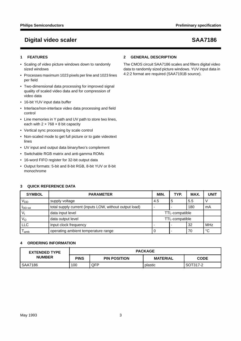
1 FEATURES
• Scaling of video picture windows down to randomlysized windows
• Processes maximum 1023 pixels per line and 1023 linesper field
• Two-dimensional data processing for improved signalquality of scaled video data and for compression ofvideo data
• 16-bit YUV input data buffer
• Interlace/non-interlace video data processing and fieldcontrol
• Line memories in Y path and UV path to store two lines,each with 2 × 768 × 8 bit capacity
• Vertical sync processing by scale control
• Non-scaled mode to get full picture or to gate videotextlines
• UV input and output data binary/two’s complement
• Switchable RGB matrix and anti-gamma ROMs
• 16-word FIFO register for 32-bit output data
• Output formats: 5-bit and 8-bit RGB, 8-bit YUV or 8-bitmonochrome
2 GENERAL DESCRIPTION
The CMOS circuit SAA7186 scales and filters digital videodata to randomly sized picture windows. YUV input data in4:2:2 format are required (SAA7191B source).
3 QUICK REFERENCE DATA
4 ORDERING INFORMATION
SYMBOL PARAMETER MIN. TYP. MAX. UNIT
VDD supply voltage 4.5 5 5.5 V
IDD tot total supply current (inputs LOW, without output load) - - 180 mA
VI data input level TTL-compatible
VO data output level TTL-compatible
LLC input clock frequency - - 32 MHz
Tamb operating ambient temperature range 0 - 70 °C
EXTENDED TYPENUMBER
PACKAGE
PINS PIN POSITION MATERIAL CODE
SAA7186 100 QFP plastic SOT317-2
May 1993 4
Philips Semiconductors Preliminary specification
Digital video scaler SAA7186
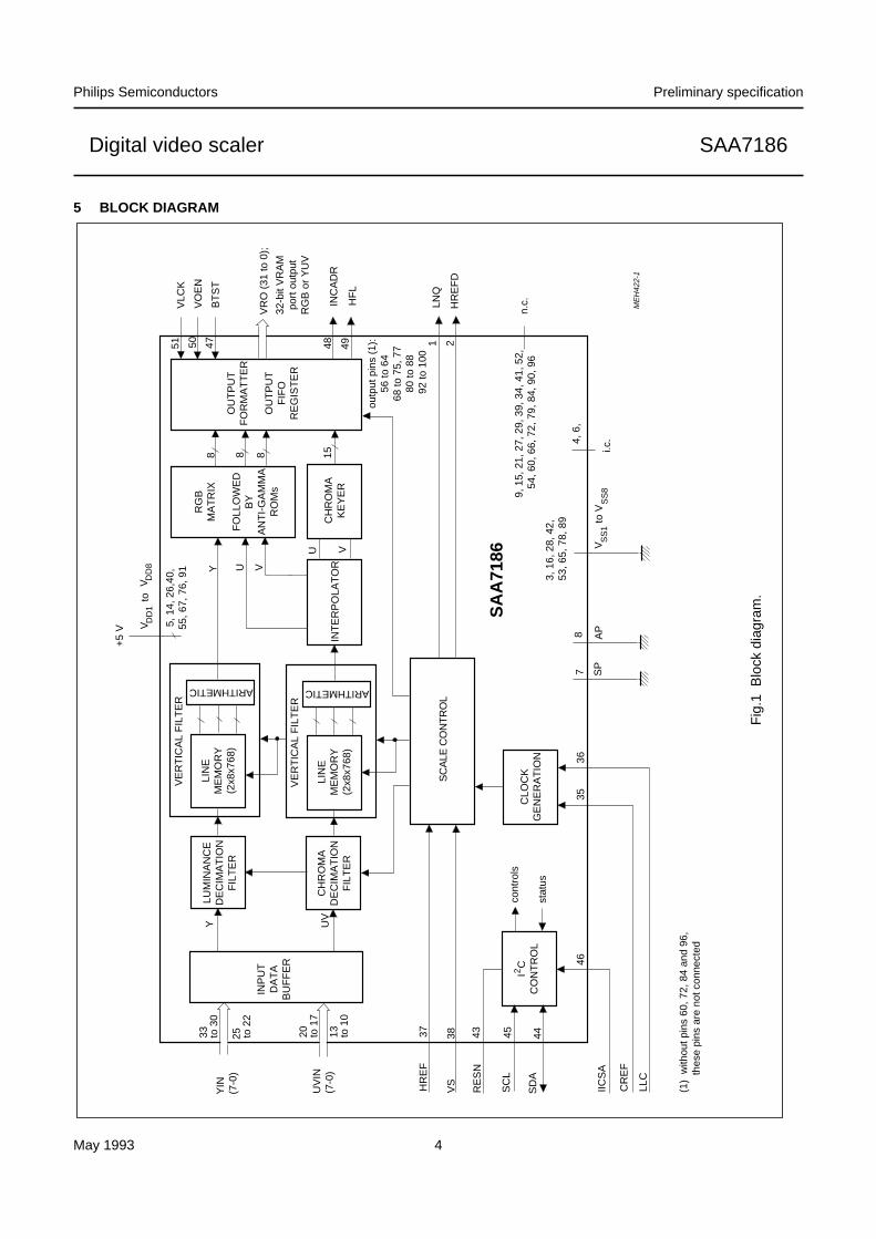
5 BLOCK DIAGRAM
handbook, full pagewidth
SA
A71
86
SC
ALE
CO
NT
RO
L
I C
CO
NT
RO
L
VE
RT
ICA
L F
ILT
ER
INT
ER
PO
LAT
OR
VS
S1
V DD
1
VR
O (
31 to
0);
49
ME
H42
2-1
Fig
.1 B
lock
dia
gram
.
INP
UT
DA
TA
BU
FF
ER
20
to 1
7
LUM
INA
NC
ED
EC
IMA
TIO
NF
ILT
ER
CH
RO
MA
DE
CIM
AT
ION
FIL
TE
R
ARITHMETIC
LIN
EM
EM
OR
Y(2
x8x7
68)
VE
RT
ICA
L F
ILT
ER
ARITHMETIC
LIN
EM
EM
OR
Y(2
x8x7
68)
RG
BM
AT
RIX
FO
LLO
WE
DB
YA
NT
I-G
AM
MA
RO
Ms
CH
RO
MA
KE
YE
R
OU
TP
UT
FO
RM
AT
TE
R
OU
TP
UT
FIF
OR
EG
IST
ER
2C
LOC
KG
EN
ER
AT
ION 36
3546
4445
SD
A
SC
L
IICS
A
CR
EF
(1)
with
out p
ins
60, 7
2, 8
4 an
d 96
,
th
ese
pins
are
not
con
nect
ed
RE
SN
UV
IN(7
-0)
YIN
(7-0
)
13
to 1
0
25
to
22
33
to 3
0Y U
V
Y U V
U V
88 158
48475051V
LCK
VO
EN
BT
ST
INC
AD
R
HF
L
+5
V 5, 1
4, 2
6,40
,55
, 67,
76,
91
toV D
D8
78
SP
AP
3, 1
6, 2
8, 4
2,
53, 6
5, 7
8, 8
9
i.c.4,
6,
to V
SS
8
43
HR
EF
VS
37
38
32-b
it V
RA
Mpo
rt o
utpu
tR
GB
or
YU
V
n.c.
9, 1
5, 2
1, 2
7, 2
9, 3
9, 3
4, 4
1, 5
2,
54, 6
0, 6
6, 7
2, 7
9, 8
4, 9
0, 9
6
outp
ut p
ins
(1):
56 to
64
68 to
75,
77
80 to
88
92
to 1
00
cont
rols
stat
us
LNQ
HR
EF
D
1 2
LLC
Fig
.1 B
lock
dia
gram
.

May 1993 5
Philips Semiconductors Preliminary specification
Digital video scaler SAA7186
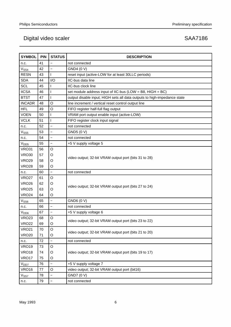
6 PINNING
SYMBOL PIN STATUS DESCRIPTION
LNQ 1 O line qualifier signal; active polarity defined by QPL-bit in “10” (VCLK strobed)
HREFD 2 O delay-compensated HREF output signal (VCLK strobed)
VSS1 3 − GND1 (0 V)
i.c. 4 − internally connected
VDD1 5 − +5 V supply voltage 1
i.c. 6 − internally connected
SP 7 I connected to ground (shift pin for testing)
AP 8 I connected to ground (action pin for testing)
n.c. 9 − not connected
UVIN0 10 I
time-multiplexed colour-difference input data (bits 0 to 3)UVIN1 11 I
UVIN2 12 I
UVIN3 13 I
VDD2 14 − +5 V supply voltage 2
n.c. 15 − not connected
VSS2 16 − GND2 (0 V)
UVIN4 17 I
time-multiplexed colour-difference input data (bits 4 to 7)UVIN5 18 I
UVIN6 19 I
UVIN7 20 I
n.c. 21 − not connected
YIN0 22 I
luminance input data (bits 0 to 3)YIN1 23 I
YIN2 24 I
YIN3 25 I
VDD3 26 − +5 V supply voltage 3
n.c. 27 − not connected
VSS3 28 − GND3 (0 V)
n.c. 29 − not connected
YIN4 30 I
luminance input data (bits 4 to 7)YIN5 31 I
YIN6 32 I
YIN7 33 I
n.c. 34 − not connected
CREF 35 I clock reference, external sync signal
LLC 36 I line-locked system clock input signal (twice of pixel rate)
HREF 37 I horizontal reference, pixel data clock signal (also present during vertical blanking)
VS 38 I vertical sync input signal (approximately 6 lines long)
n.c. 39 − not connected
VDD4 40 − +5 V supply voltage 4
May 1993 6
Philips Semiconductors Preliminary specification
Digital video scaler SAA7186
n.c. 41 − not connected
VSS4 42 − GND4 (0 V)
RESN 43 I reset input (active-LOW for at least 30LLC periods)
SDA 44 I/O IIC-bus data line
SCL 45 I IIC-bus clock line
IICSA 46 I set module address input of IIC-bus (LOW = B8, HIGH = BC)
BTST 47 I output disable input; HIGH sets all data outputs to high-impedance state
INCADR 48 O line increment / vertical reset control output line
HFL 49 O FIFO register half-full flag output
VOEN 50 I VRAM port output enable input (active-LOW)
VCLK 51 I FIFO register clock input signal
n.c. 52 − not connected
VSS5 53 − GND5 (0 V)
n.c. 54 − not connected
VDD5 55 − +5 V supply voltage 5
VRO31 56 O
video output; 32-bit VRAM output port (bits 31 to 28)VRO30 57 O
VRO29 58 O
VRO28 59 O
n.c. 60 − not connected
VRO27 61 O
video output; 32-bit VRAM output port (bits 27 to 24)VRO26 62 O
VRO25 63 O
VRO24 64 O
VSS6 65 − GND6 (0 V)
n.c. 66 − not connected
VDD6 67 − +5 V supply voltage 6
VRO23 68 Ovideo output; 32-bit VRAM output port (bits 23 to 22)
VRO22 69 O
VRO21 70 Ovideo output; 32-bit VRAM output port (bits 21 to 20)
VRO20 71 O
n.c. 72 − not connected
VRO19 73 O
video output; 32-bit VRAM output port (bits 19 to 17)VRO18 74 O
VRO17 75 O
VDD7 76 − +5 V supply voltage 7
VRO16 77 O video output; 32-bit VRAM output port (bit16)
VSS7 78 − GND7 (0 V)
n.c. 79 − not connected
SYMBOL PIN STATUS DESCRIPTION

May 1993 7
Philips Semiconductors Preliminary specification
Digital video scaler SAA7186
VRO15 80 O
video output; 32-bit VRAM output port (bits 15 to 12)VRO14 81 O
VRO13 82 O
VRO12 83 O
n.c. 84 − not connected
VRO11 85 O
video output; 32-bit VRAM output port (bits 11 to 8)VRO10 86 O
VRO9 87 O
VRO8 88 O
VSS8 89 O GND8 (0 V)
n.c. 90 − not connected
VDD8 91 − +5 V supply voltage 8
VRO7 92 O
video output; 32-bit VRAM output port (bits 7 to 4)VRO6 93 O
VRO5 94 O
VRO4 95 O
n.c. 96 − not connected
VRO3 97 O
video output; 32-bit VRAM output port (bits 3 to 0)VRO2 98 O
VRO1 99 O
VRO0 100 O
SYMBOL PIN STATUS DESCRIPTION

May 1993 8
Philips Semiconductors Preliminary specification
Digital video scaler SAA7186
6.1 Pin configuration
Fig.2 Pin configuration.
handbook, full pagewidth
SAA7186
87 8283848586
2
4
1
3
9596979899 94 8990919293 88
MEH421
6
5
7
LNQ
SS1
8
9
10
11
12
17
16
15
14
13
18
19
81100
HREFD.
i.c.
V
i.c.
DD2 V
SS2V
DD1V
SP.
AP
UVIN0
n.c.
UVIN1
UVIN2
UVIN3
n.c.
UVIN4
UVIN5
UVIN6
20UVIN7
21
22
23
24
25
n.c.
YIN0
YIN2
YIN3
YIN1
4439 43424140 45 504948474631 32 3736353433 38
VYIN
5
YIN
6
YIN
7
CR
EF
LLC
HR
EF
VSn.c.
n.c. DD
4
VS
S4
n.c.
RE
SN
SD
A
SC
L
IICS
A
BT
ST
INC
AD
R
HF
L
VO
EN
VD
D8
n.c.
VS
S8
n.c.
VR
O0
n.c.
VR
O1
VR
O2
VR
O3
VR
O4
VR
O5
VR
O6
VR
O7
VR
O8
VR
O9
VR
O10
VR
O11
VR
O12
VR
O13
VR
O14
26
27
28
29
30
n.c.
YIN4
SS3V
DD3V
n.c.52
53
54
55
56
57
58
59
60
61
62
63
51
68
69
70
64
65
66
67
SS6
DD6V
76
77
78
79
80 VRO15
VRO16
n.c.
VRO21
VRO22
VRO23
n.c.
VRO24
VRO25
VRO26
VRO27
n.c.
V
VRO28
VRO29
VRO30
VRO31
n.c.
DD5V
SS5V
n.c.
VCLK
71
72
73
74
75 VRO17
VRO18
VRO19
n.c.
VRO20
DD7V
SS7V
May 1993 9
Philips Semiconductors Preliminary specification
Digital video scaler SAA7186
7 FUNCTIONAL DESCRIPTION
The input port is output of Philips digital videomultistandard decoders (SAA7151B, SAA7191B) or othersimilar sources.The SAA7186 input supports the 16-bit YUV 4:2:2 format.The video data from the input port are converted into aunique internal two’s complement data stream and areprocessed in horizontal direction in two separatedecimation filters. Then they are processed in verticaldirection by the vertical processing unit (VPU).Chrominance data are interpolated to a 4:4:4 format; achroma keying bit is generated.The 4:4:4 YUV data are then converted from the YUV tothe RGB domain in a digital matrix. ROM tables in the RGBdata path can be used for anti-gamma correction ofgamma-corrected input signals.Uncorrected RGB and YUV signals can be bypassed.A scale control unit generates reference and gate signalsfor scaling of the processed video data. After dataformatting to the various VRAM port formats, the scaledvideo data are buffered in the 16 word × 32-bit output FIFOregister. The FIFO output is directly connected to theVRAM output bus VRO(31-0). Specific reference signalssupport an easy memory interfacing.All functions of the SAA7186 are controlled via I2C-bususing 17 subaddresses. The external microcontroller canget information by reading the status register.
7.1 Video input port
The 16-bit YUV input data in 4:2:2 format (Table 1) consistof 8-bit luminance data Y (pins YIN(7-0)) and 8-bittime-multiplexed colour-difference data UV (pinsUVIN(7-0)).The input data are clocked in by the signals LLC andCREF (Fig.3). HREF and VS inputs define the video scanpattern (window).
Sequential input data
• are limited to maximum 768 active pixels per line if thevertical filter is active
• UV can be processed in straight binary and two’scomplement representation (controlled by TCC)
7.2 Decimation filters
The decimation filters perform accurate horizontal filteringof the input data stream.Signal characteristics are matched in front of the pixeldecimation stage, thus disturbing artifacts, caused by thepixel dropping, are reduced. The signal bandwidth can bereduced in steps of:
2-tap filter = −6 dB at 0.325 pixel rate
3-tap filter = −6 dB at 0.25 pixel rate
4-tap filter = −6 dB at 0.21 pixel rate
5-tap filter = −6 dB at 0.125 pixel rate
9-tap filter = −6 dB at 0.075 pixel rate
The different characteristics are chosen dependent on thedefined scaling parameters in an adaptive filter mode(AFS-bit = 1).The filter characteristics can also be selectedindependently by control bits HF2 to HF0 at AFS-bit = 0.
7.3 Vertical filters
Y and UV data are handled in separate filters (Fig.1). Eachof the two line memories has a capacity of 2 × 768 × 8-bit.Thus two complete video lines of 4:2:2 YUV data can bestored. The VPU is split into two memory banks and onearithmetic unit. The available processing modes,respectively transfer functions, are selectable by the bitsVP1 and VP0 if AFS = 0.An adaptive mode is selected by AFS = 1. Disturbingartifacts, generated by line dropping, are reduced.
Adaptive filter selection (AFS = 1):
SCALING RATIOFILTER FUNCTION
(REFER TO I2C SECTION)
XD/XS horizontal
≤1≤14/15≤11/15≤7/15≤3/15
bypassedfilter 1filter 6filter 3filter 4
YD/YS vertical
≤1≤13/15≤4/15
bypassedfilter 1filter 2
May 1993 10
Philips Semiconductors Preliminary specification
Digital video scaler SAA7186
7.4 RGB matrix
Y data and UV data are converted after interpolation intoRGB data according to CCIR601 recommendation. Dataare bypassed in YUV or monochrome modes.
Table 1 4 : 2 : 2 format (pixels per line). The time framesare controlled by the HREF signal.
Note
1. e = even pixel; o = odd pixel
The matrix equations are these considering the digitalquantization:
R = Y + 1.375 V
G = Y − 0.703125 V − 0.34375 U
B = Y + 1.734375 U.
Anti-gamma ROM tables:ROM tables are implemented at the matrix output toprovide anti-gamma correction of the RGB data. A curvefor a gamma of 1.4 is implemented
The tables can be used (RTB-bit = 0) to compensategamma correction for linear data representation of RGBoutput data.
INPUT PIXEL BYTE SEQUENCE
YIN7YIN6YIN5YIN4YIN3YIN2YIN1YIN0
Ye7Ye6Ye5Ye4Ye3Ye2Ye1Ye0
Yo7Yo6Yo5Yo4Yo3Yo2Yo1Yo0
Ye7Ye6Ye5Ye4Ye3Ye2Ye1Ye0
Yo7Yo6Yo5Yo4Yo3Yo2Yo1Yo0
Ye7Ye6Ye5Ye4Ye3Ye2Ye1Ye0
UVIN7UVIN6UVIN5UVIN4UVIN3UVIN2UVIN1UVIN0
Ue7Ue6Ue5Ue4Ue3Ue2Ue1Ue0
Ve7Ve6Ve5Ve4Ve3Ve2Ve1Ve0
Ue7Ue6Ue5Ue4Ue3Ue2Ue1Ue0
Ve7Ve6Ve5Ve4Ve3Ve2Ve1Ve0
Ue7Ue6Ue5Ue4Ue3Ue2Ue1Ue0
Y frame 0 1 2 3 4
UV frame 0 2 4
7.5 Chrominance signal keyer
The keyer generates an alpha signal to achieve a 5-5-5 +αRGB alpha output signal. Therefore, the processed UVdata amplitudes are compared with thresholds set viaI2C-bus (subaddresses ”0C to 0F”). A logical “1” signal isgenerated if the amplitude is inside the specified amplituderange, otherwise a logical “0” is generated.Keying can be switched off by setting the lower limit higherthan the upper limit (“0C or 0E” and “0D or 0F”).
7.6 Scale control and vertical regions
The scale control block SC includes verticaladdress/sequence counters to define the current positionin the input field and to address the internal VPUmemories.To perform scaling, XD of XS pixel selection in horizontaldirection and YD of YS line selection in vertical directionare applied. The pixel and line dropping are controlled atthe input of the FIFO register. To control the decimationfilter function and the vertical data processing in theadaptive mode (AFS = 1), the scaling ratio in horizontaland vertical direction is estimated in the SC block.
The input field can be divided into two vertical regions− the bypass region and the scaling region, which aredefined via I2C-bus by the parameters VS, VC, YO andYS.
Vertical bypass region:
Data are not scaled and independent of I2C-bits FS1, FS0the output format is always 8-bit greyscale (monochrome).The SAA7186 outputs all active pixels of a line, defined bythe HREF input signal if the vertical bypass region isactive. This can be used, for example, to store videotextinformation in the field memory.
The start line of the bypass region is defined by VS; thenumber of lines to be bypassed is defined by VC.
Vertical scaling region:
Data is scaled with start at line YO and the output formatis selected when FS1, FS0 are valid.This is the “normal operation” area.
The input/output screen dimensions in horizontal andvertical direction are defined by the parameters
XO, XS and XD for horizontal
YO, YS and YD for vertical.
The circuit processes XS samples of a line. Remainingpixels are ignored if a line is longer than XS. If a line is

May 1993 11
Philips Semiconductors Preliminary specification
Digital video scaler SAA7186
shorter than XS, processing is aborted when the fallingedge of HREF is detected.
Vertical regions in Fig.4:
• the two regions can be programmed via I2C-bus,whereby regions should not overlap (active regionoverrides the bypass region).
• the start of a normal active picture depends on videostandard and has to be programmed to the correctvalue.
• the offsets XO and YO have to be set according to theinternal processing delays to ensure the completenumber of destination pixels and lines (Table 6).
• the scaling parameters can be used to perform apanning function over the video frame/field.
Fig.3 Horizontal and data multiplex timing.
handbook, full pagewidthLLC
CREF
HREFend ofactive line
Byte number for pixels:
Y signal
U and V signal
n – 5
Vn-5
n – 4
Un-3
n – 3
Vn-3
n – 2
Un-1
n – 1
Vn-1
n
Un-5
MEH410
handbook, full pagewidthLLC
CREF
HREFstart ofactive line
0
U0
1
V0
2
U2
3
V2
4
U4
5
V4
6
U6
7
V6
Y signal
U and V signal
Byte numbers for pixles:
MEH411
May 1993 12
Philips Semiconductors Preliminary specification
Digital video scaler SAA7186
7.7 Output data representation and levels
Output data representation of the YUV data can bemodified by bit MCT (subaddress 10).The DC gain is 1 for YUV input data. The correspondingRGB levels are defined by the matrix equations. Theluminance levels are limited according to CCIR 601
16 (239) = black235 (20) = white(..) = greyscale luminance levels
if the YUV or monochrome luminance output formats areselected.
The signal levels of the RGB formats are limited in 8-bit to“0” or “255”. For the 5-bit RGB formats a truncation from8-bit to 5-bit is implemented.
Fill values are inserted dependent on longword positionand destination size:
• “0” in RGB formats and for Y two’s complement U, V
• “128” for U, V (straight binary)
• “255” in 8-bit greyscale format
The unused output values of the YUV and greyscaleformats can be used for other purposes.
Fig.4 Vertical regions.
handbook, full pagewidth
MEH357-1
scaling region
vertical bypass start
first valid line
bypass region
verticalblanking
vertical sync
scaling region start
VS
vertical bypass countequals VS
YO
scaling region countequals YS Y-size source
May 1993 13
Philips Semiconductors Preliminary specification
Digital video scaler SAA7186
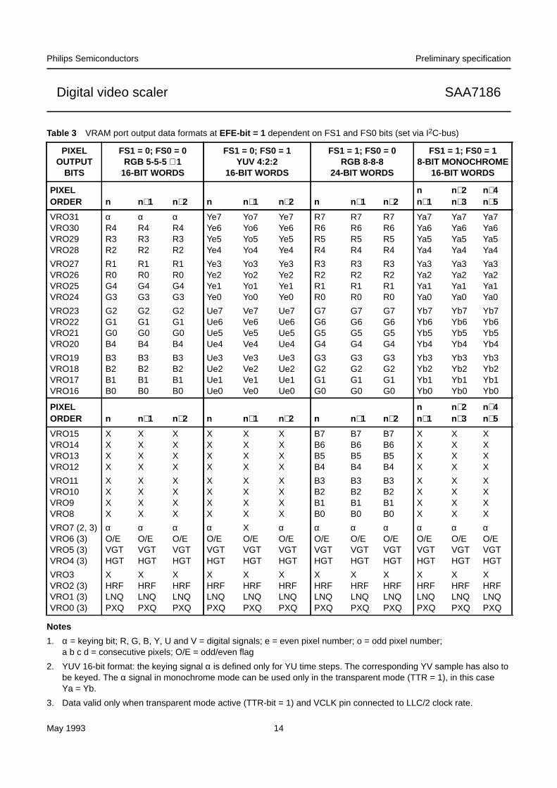
Table 2 VRAM port output data formats at EFE-bit = 0 dependent on FS1 and FS0 bits (set via I2C-bus)
Note
1. α = keying bit; R, G, B, Y, U and V = digital signals; e = even pixel number; o = odd pixel number;a b c d = consecutive pixels
PIXELOUTPUT
BITS
FS1 = 0; FS0 = 0RGB 5-5-5 + 1
32-BIT WORDS
FS1 = 0; FS0 = 1YUV 4:2:2
32-BIT WORDS
FS1 = 1; FS0 = 0YUV 4:2:2 TEST16-BIT WORDS
FS1 = 1; FS0 = 18-BIT MONOCHROME
32-BIT WORDS
PIXELORDER n n+2 n+4 n n+2 n+4 n n+1 n+2
nn+1
n+4n+5
n+8n+9
VRO31VRO30VRO29VRO28
αR4R3R2
αR4R3R2
αR4R3R2
Ye7Ye6Ye5Ye4
Ye7Ye6Ye5Ye4
Ye7Ye6Ye5Ye4
Ye7Ye6Ye5Ye4
Yo7Yo6Yo5Yo4
Ye7Ye6Ye5Ye4
Ya7Ya6Ya5Ya4
Ya7Ya6Ya5Ya4
Ya7Ya6Ya5Ya4
VRO27VRO26VRO25VRO24
R1R0G4G3
R1R0G4G3
R1R0G4G3
Ye3Ye2Ye1Ye0
Ye3Ye2Ye1Ye0
Ye3Ye2Ye1Ye0
Ye3Ye2Ye1Ye0
Yo3Yo2Yo1Yo0
Ye3Ye2Ye1Ye0
Ya3Ya2Ya1Ya0
Ya3Ya2Ya1Ya0
Ya3Ya2Ya1Ya0
VRO23VRO22VRO21VRO20
G2G1G0B4
G2G1G0B4
G2G1G0B4
Ue7Ue6Ue5Ue4
Ue7Ue6Ue5Ue4
Ue7Ue6Ue5Ue4
Ue7Ue6Ue5Ue4
Ve7Ve6Ve5Ve4
Ue7Ue6Ue5Ue4
Yb7Yb6Yb5Yb4
Yb7Yb6Yb5Yb4
Yb7Yb6Yb5Yb4
VRO19VRO18VRO17VRO16
B3B2B1B0
B3B2B1B0
B3B2B1B0
Ue3Ue2Ue1Ue0
Ue3Ue2Ue1Ue0
Ue3Ue2Ue1Ue0
Ue3Ue2Ue1Ue0
Ve3Ve2Ve1Ve0
Ue3Ue2Ue1Ue0
Yb3Yb2Yb1Yb0
Yb3Yb2Yb1Yb0
Yb3Yb2Yb1Yb0
PIXELORDER n+1 n+3 n+5 n+1 n+3 n+5 OUTPUTS NOT USED
n+2n+3
n+6n+7
n+10n+11
VRO15VRO14VRO13VRO12
αR4R3R2
αR4R3R2
αR4R3R2
Yo7Yo6Yo5Yo4
Yo7Yo6Yo5Yo4
Yo7Yo6Yo5Yo4
XXXX
XXXX
XXXX
Yc7Yc6Yc5Yc4
Yc7Yc6Yc5Yc4
Yc7Yc6Yc5Yc4
VRO11VRO10VRO9VRO8
R1R0G4G3
R1R0G4G3
R1R0G4G3
Yo3Yo2Yo1Yo0
Yo3Yo2Yo1Yo0
Yo3Yo2Yo1Yo0
XXXX
XXXX
XXXX
Yc3Yc2Yc1Yc0
Yc3Yc2Yc1Yc0
Yc3Yc2Yc1Yc0
VRO7VRO6VRO5VRO4
G2G1G0B4
G2G1G0B4
G2G1G0B4
Ve7Ve6Ve5Ve4
Ve7Ve6Ve5Ve4
Ve7Ve6Ve5Ve4
XXXX
XXXX
XXXX
Yd7Yd6Yd5Yd4
Yd7Yd6Yd5Yd4
Yd7Yd6Yd5Yd4
VRO3VRO2VRO1VRO0
B3B2B1B0
B3B2B1B0
B3B2B1B0
Ve3Ve2Ve1Ve0
Ve3Ve2Ve1Ve0
Ve3Ve2Ve1Ve0
XXXX
XXXX
XXXX
Yd3Yd2Yd1Yd0
Yd3Yd2Yd1Yd0
Yd3Yd2Yd1Yd0
May 1993 14
Philips Semiconductors Preliminary specification
Digital video scaler SAA7186
Table 3 VRAM port output data formats at EFE-bit = 1 dependent on FS1 and FS0 bits (set via I2C-bus)
Notes
1. α = keying bit; R, G, B, Y, U and V = digital signals; e = even pixel number; o = odd pixel number;a b c d = consecutive pixels; O/E = odd/even flag
2. YUV 16-bit format: the keying signal α is defined only for YU time steps. The corresponding YV sample has also tobe keyed. The α signal in monochrome mode can be used only in the transparent mode (TTR = 1), in this caseYa = Yb.
3. Data valid only when transparent mode active (TTR-bit = 1) and VCLK pin connected to LLC/2 clock rate.
PIXELOUTPUT
BITS
FS1 = 0; FS0 = 0RGB 5-5-5 + 1
16-BIT WORDS
FS1 = 0; FS0 = 1YUV 4:2:2
16-BIT WORDS
FS1 = 1; FS0 = 0RGB 8-8-8
24-BIT WORDS
FS1 = 1; FS0 = 18-BIT MONOCHROME
16-BIT WORDS
PIXELORDER n n+1 n+2 n n+1 n+2 n n+1 n+2
nn+1
n+2n+3
n+4n+5
VRO31VRO30VRO29VRO28
αR4R3R2
αR4R3R2
αR4R3R2
Ye7Ye6Ye5Ye4
Yo7Yo6Yo5Yo4
Ye7Ye6Ye5Ye4
R7R6R5R4
R7R6R5R4
R7R6R5R4
Ya7Ya6Ya5Ya4
Ya7Ya6Ya5Ya4
Ya7Ya6Ya5Ya4
VRO27VRO26VRO25VRO24
R1R0G4G3
R1R0G4G3
R1R0G4G3
Ye3Ye2Ye1Ye0
Yo3Yo2Yo1Yo0
Ye3Ye2Ye1Ye0
R3R2R1R0
R3R2R1R0
R3R2R1R0
Ya3Ya2Ya1Ya0
Ya3Ya2Ya1Ya0
Ya3Ya2Ya1Ya0
VRO23VRO22VRO21VRO20
G2G1G0B4
G2G1G0B4
G2G1G0B4
Ue7Ue6Ue5Ue4
Ve7Ve6Ve5Ve4
Ue7Ue6Ue5Ue4
G7G6G5G4
G7G6G5G4
G7G6G5G4
Yb7Yb6Yb5Yb4
Yb7Yb6Yb5Yb4
Yb7Yb6Yb5Yb4
VRO19VRO18VRO17VRO16
B3B2B1B0
B3B2B1B0
B3B2B1B0
Ue3Ue2Ue1Ue0
Ve3Ve2Ve1Ve0
Ue3Ue2Ue1Ue0
G3G2G1G0
G3G2G1G0
G3G2G1G0
Yb3Yb2Yb1Yb0
Yb3Yb2Yb1Yb0
Yb3Yb2Yb1Yb0
PIXELORDER n n+1 n+2 n n+1 n+2 n n+1 n+2
nn+1
n+2n+3
n+4n+5
VRO15VRO14VRO13VRO12
XXXX
XXXX
XXXX
XXXX
XXXX
XXXX
B7B6B5B4
B7B6B5B4
B7B6B5B4
XXXX
XXXX
XXXX
VRO11VRO10VRO9VRO8
XXXX
XXXX
XXXX
XXXX
XXXX
XXXX
B3B2B1B0
B3B2B1B0
B3B2B1B0
XXXX
XXXX
XXXX
VRO7 (2, 3)VRO6 (3)VRO5 (3)VRO4 (3)
αO/EVGTHGT
αO/EVGTHGT
αO/EVGTHGT
αO/EVGTHGT
XO/EVGTHGT
αO/EVGTHGT
αO/EVGTHGT
αO/EVGTHGT
αO/EVGTHGT
αO/EVGTHGT
αO/EVGTHGT
αO/EVGTHGT
VRO3VRO2 (3)VRO1 (3)VRO0 (3)
XHRFLNQPXQ
XHRFLNQPXQ
XHRFLNQPXQ
XHRFLNQPXQ
XHRFLNQPXQ
XHRFLNQPXQ
XHRFLNQPXQ
XHRFLNQPXQ
XHRFLNQPXQ
XHRFLNQPXQ
XHRFLNQPXQ
XHRFLNQPXQ
May 1993 15
Philips Semiconductors Preliminary specification
Digital video scaler SAA7186
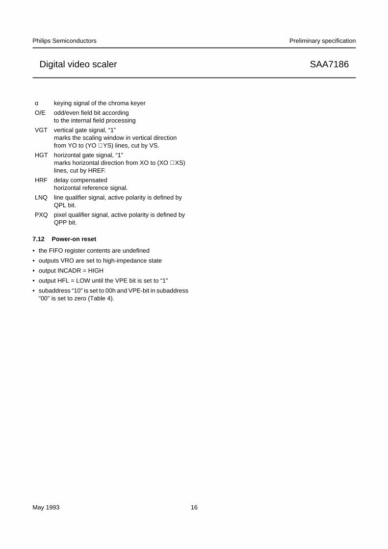
7.8 Output FIFO register and VRAM output port
The output FIFO register is the buffer between the videodata stream and the VRAM data input port. Resized videodata are buffered and formatted. 32-, 24- and 16-bit videodata modes are supported. The various formats areselected by the bits EFE, FS1 and FS0. VRAM portformats are shown in Tables 2 and 3. The FIFO registercapacity is 16 word × 32 bit (for 32-, 24-, or 16-bit videodata). The bits LW1 and LW0 can be used to define theposition of the first pixel each line in the 32-bit longwordformats or to shift the UV sequence to VU in the 16-bit YUVformats (LW1 = 1).
VRAM port inputs are:VCLK to clock the FIFO register output data and VOEN toenable output data.
VRAM port outputs are:the HFL flag (half-full flag), the signal INCADR (refer tosection “data burst transfer”) and the reference signals forpixel and line selection on outputs VRO(7-0) (only for 24-and 16-bit video data formats refer to “transparent datatransfer”).
7.9 VRAM port transfer procedures
Data transfer on the VRAM port can be doneasynchronously controlled by outputs HFL, INCADR andinput VCLK (data burst transfer with bit TTR = 0).
Data transfer on the VRAM port can be donesynchronously controlled by output reference signals onoutputs VRO(7-0) and a clock rate of LLC/2 on input VCLK(transparent data transfer with bit TTR = 1 and EFE = 1).The scaling capability of the SAA7186 can be used invarious applications.
7.10 Data burst transfer mode
Data transfer on the VRAM port is asynchronously(TTR = 0). This mode can be used for all output formats.Four signals for communication with the external memoryare provided.
• HFL flag, the half-full flag of the FIFO output register israised when the FIFO contains at least 8 data words(HFL = HIGH). By setting HFL = 1, the SAA7186requests a data burst transfer by the external memorycontroller, that has to start a transfer cycle within thenext 32 LLC cycles for 32-bit longword modes (16 LLCcycles for 16- and 24-bit modes). If there are pixels in theFIFO at the end of a line, which are not transferred, thecircuit fills up the FIFO register with “fill pixels” until it ishalf-full and sets the HFL flag to request a data bursttransfer. After transfer is done, HFL is used in
combination with INCADR to indicate the lineincrements (Figures 6 and 7).
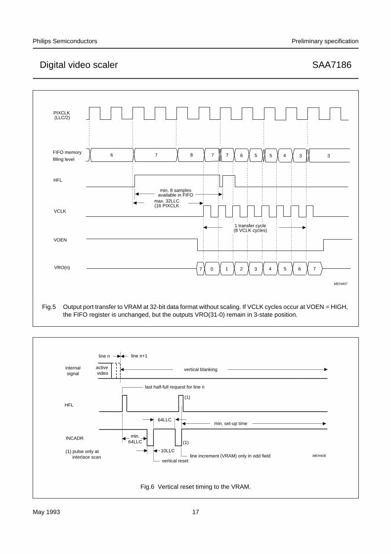
• INCADR output signal is used in combination with HFLto control horizontal and vertical address generation fora memory controller. The pulse sequence depends onfield formats (interlace/ non-interlace or odd/even fields,Figures 6 and 7) and control bits OF (subaddress 00).
HFL = 1 at the rising edge of INCADR:
the end of line is reached, request for line addressincrement
HFL = 0 at the rising edge of INCADR:
the end of field/frame is reached, request for line andpixel addresses reset
(The distance from the last half-full request HFL to theINCADR pulse may be longer than 64 × LLC. The HFLstate is defined for minimum 4 × LLC in front of the risingedge of INCADR and minimum 2 × LLC afterwards.)
• VCLK input signal to clock the FIFO register output dataVRO(n). New data are placed on the VRO(n) port withthe rising edge of VCLK (Fig.5).
• VOEN input enables output data VRO(n). The outputsare in 3-state mode at VOEN = HIGH. VOEN changesonly when VCLK is LOW. If VCLK pulses are appliedduring VOEN = HIGH, the outputs remain inactive, butthe FIFO register accepts the pulses.
7.11 Transparent data transfer mode
Data transfer on the VRAM port can be achievedsynchronously (TTR = 1). With a continuous clock rate ofLLC/2 on input VCLK, the SAA7186 delivers acontinuously processed data stream. Therefore, theextended formats of the VRAM output port have to beselected (bit EFE = 1; Table 3). The reference and gatesignals on outputs VRO(6-1) and the LNQ signal aredelivered in each field (means scaled and ignored fields).The PXO signal (also VRO0) is only delivered in activefields. The output signals VRO(7-0) can be used to bufferqualified pre-processed RGB or YUV video data (notice:the YUV data are only valid in qualified time slots). Controloutput signals in Table 3 are:
May 1993 16
Philips Semiconductors Preliminary specification
Digital video scaler SAA7186
7.12 Power-on reset
• the FIFO register contents are undefined
• outputs VRO are set to high-impedance state
• output INCADR = HIGH
• output HFL = LOW until the VPE bit is set to “1”
• subaddress “10” is set to 00h and VPE-bit in subaddress“00” is set to zero (Table 4).
α keying signal of the chroma keyer
O/E odd/even field bit accordingto the internal field processing
VGT vertical gate signal, “1”marks the scaling window in vertical directionfrom YO to (YO + YS) lines, cut by VS.
HGT horizontal gate signal, “1”marks horizontal direction from XO to (XO + XS)lines, cut by HREF.
HRF delay compensatedhorizontal reference signal.
LNQ line qualifier signal, active polarity is defined byQPL bit.
PXQ pixel qualifier signal, active polarity is defined byQPP bit.
May 1993 17
Philips Semiconductors Preliminary specification
Digital video scaler SAA7186
Fig.5 Output port transfer to VRAM at 32-bit data format without scaling. If VCLK cycles occur at VOEN = HIGH,the FIFO register is unchanged, but the outputs VRO(31-0) remain in 3-state position.
handbook, full pagewidth
MEH407
PIXCLK(LLC/2)
FIFO memory
filling level6 7 8 7 7 6 5 5 4 3 3
7 1 2 3 4 5 60 7
HFL
VCLK
VOEN
VRO(n)
min. 8 samples available in FIFO
max. 32LLC(16 PIXCLK
1 transfer cycle(8 VCLK cycles)
Fig.6 Vertical reset timing to the VRAM.
handbook, full pagewidth
MEH406
min.64LLC
min. set-up time
vertical blankingactive video
64LLC
10LLC
line n line n+1
(1)
(1) pulse only at interlace scan line increment (VRAM) only in odd field
(1)
internalsignal
HFL
INCADR
last half-full request for line n
vertical reset

May 1993 18
Philips Semiconductors Preliminary specification
Digital video scaler SAA7186
Fig.7 Horizontal increment timing to the VRAM.
handbook, full pagewidth
MEH405-1
min.64LLC
min. set-up time
horizontal blankingactive video
active video
64LLC
2LLC
6LLC
6LLC
10LLC
line n line n+1
(1)
(1) pulse only at interlace scan line increment (VRAM)
(1)
internalsignal
HFL
INCADR
last half-full request for line n first half-full request for line n+1
Fig.8 Reference signals for scaling window.

May 1993 19
Philips Semiconductors Preliminary specification
Digital video scaler SAA7186
7.13 Field processing
The phase of the field sequence (odd/even dependent oninputs HREF and VS) is detected by means of the fallingedge of VS. The current field phase is reported in thestatus byte by the OEF bit (Table 5). OEF bit can be stable0 or 1 for non-interlaced input frames or non standard inputsignals VS and/or HREF (nominal condition for VS andHREF − SAA7191 B with active vertical noise limiter). Afree-running odd/even flag is generated for internal fieldprocessing if the detection reports a stable OEF bit.
The POE bit (subaddress 0B) can be used to change thepolarity of the internal flag (in case of non-standard VS andHREF signals) to control the phase of the free-running flag,and to compensate mis-detections. Thus, the SAA7186can be used under various VS/HREF timing conditions.
The SAA7186 operates on fields. To support progressivedisplays and to avoid movement blurring and artifacts, thecircuit can process both or single fields of interlaced ornon-interlaced input data. Therefore the OF bits can beused. The bits OF1 and OF0 (Table 6) determine theINCADR/HFL generation in “data burst transfer mode”.One of the fields (odd or even) is ignored when OF1 = 1;then no line increment sequence (INCADR/HFL) isgenerated, the vertical reset pulse is only generated.
With OF1 = OF0 = 0 the circuit supports correct interlaceddata storage. Two INCADR/HFL sequences are generatedin each qualified line; additionally an INCADR/HFLsequence after the vertical reset sequence of an odd fieldis generated. Thereby, the scaled lines are automaticallystored in the right sequence.
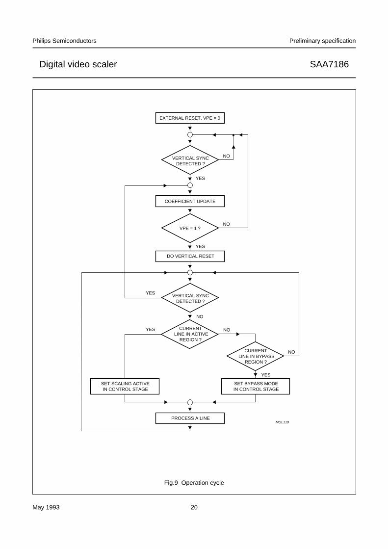
8 OPERATION CYCLE
The operation is synchronized by the input field. The cycleis specified in the flow chart (Fig.9).The circuit is inactive after power-on reset, VPO is 0 andthe FIFO control is set “empty”. The internal controlregisters are updated with the falling edge of VS signal.The circuit is switched active and waits for a transmissionof VS and a vertical reset sequence to the memorycontroller. Afterwards, the circuit waits for the beginning ofa scaling or bypass region. The processing of a current lineis finished when a vertical sync pulse appears. The circuitperforms a coefficient update and generates a new verticalreset (if it is still active).
Line processing starts when a line is decided to be active,the circuit starts to scale it. Active pixels are loaded into theFIFO register. An HFL flag is generated to initialize a datatransfer when eight words are completed. The line end isreached when the programmed pixel number is processedor when a horizontal sync pulse occurs. If there are pixelsin the FIFO register, it is filled up until it is half-full to causea data transfer. Horizontal increment pulses aretransmitted after this data transfer.
Remarks:The SAA7186 will always wait for the HREF/VS pulsebefore the line increment/vertical reset sequence isperformed. After each line/field, the FIFO control is set toempty when INCADR/HFL sequence is transmitted.No additional actions are necessary if the memorycontroller has ignored the HFL signal. There is no need tohandle overflow/underflow of the FIFO register.
May 1993 20
Philips Semiconductors Preliminary specification
Digital video scaler SAA7186
Fig.9 Operation cycle
handbook, full pagewidth
MGL119
EXTERNAL RESET, VPE = 0
VERTICAL SYNCDETECTED ?
COEFFICIENT UPDATE
DO VERTICAL RESET
YES
YES
YES
YES
NO
NO
NO
NO
NO
PROCESS A LINE
SET BYPASS MODEIN CONTROL STAGE
SET SCALING ACTIVEIN CONTROL STAGE
YES
VERTICAL SYNCDETECTED ?
CURRENT LINE IN ACTIVE
REGION ?
CURRENT LINE IN BYPASS
REGION ?
VPE = 1 ?

May 1993 21
Philips Semiconductors Preliminary specification
Digital video scaler SAA7186
Fig.10 SAA7186 system configuration in Data Burst Transfer Mode (TTR = , VCLK = continuous).
handbook, full pagewidth
MEH554
ADCTDA8708A
DMSDSAA7151B/91B
DVSSAA7186
RAMVIDEO
GRAPHICS
SCGCSAA7157/97
CPUSYSTEM
RAM
MEMORYCONTROLLER
BUFFER
data bus
address / control bus
systemclock
VCLKVOEN
HFLINCADR
RGB/YUV
display data
address
control
YUVformat 4.2:2
LLC / CREF
LFCO
CVBS
CVBS
digital
HREF / VS
Fig.11 SAA7186 system configuration in Transparent Data Transfer Mode (TTR = 1, EFE = 1,VCLK = continuous (_LLC2)).
handbook, full pagewidth
MEH555
ADCTDA8708A
DMSDSAA7151B/91B
DVSSAA7186
RAMVIDEO
GRAPHICS
SCGCSAA7157/97
MEMORYCONTROLLER
RGB/YUV
display data
address
write
YUVformat 4.2:2
LLC / CREF
LFCO
CVBS
CVBS
digital
HREF / VSFIFO
BUFFER
(VRO(31-8))
INVLLC2
VCLK = LLC2
VOEN = 1
qualifier and references(VRO(7-0))
controlread
May 1993 22
Philips Semiconductors Preliminary specification
Digital video scaler SAA7186
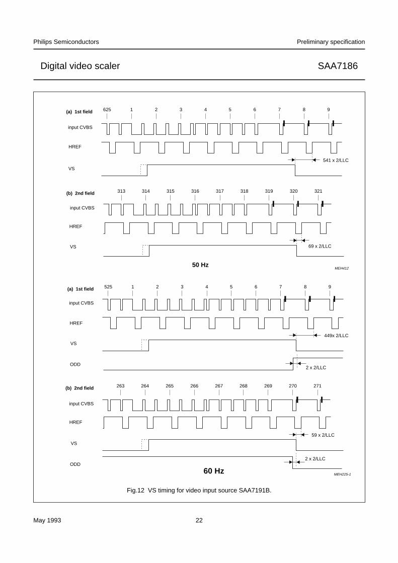
Fig.12 VS timing for video input source SAA7191B.
handbook, full pagewidth
(a) 1st field
MEH412
input CVBS
HREF
VS
625 1 2 3 4 5 6 7 8 9
541 x 2/LLC
(b) 2nd field
input CVBS
HREF
VS
313 314 315 316 317 318 319 320 321
69 x 2/LLC
handbook, full pagewidth(a) 1st field
MEH225-1
input CVBS
HREF
VS
525 1 2 3 4 5 6 7 8 9
449x 2/LLC
(b) 2nd field
input CVBS
HREF
VS
263 264 265 266 267 268 269 270 271
59 x 2/LLC
ODD
ODD
2 x 2/LLC
2 x 2/LLC
60 Hz
50 Hz
May 1993 23
Philips Semiconductors Preliminary specification
Digital video scaler SAA7186
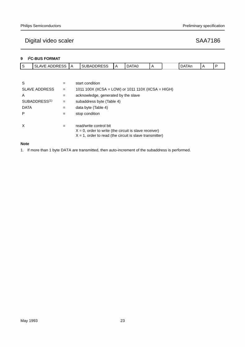
9 I2C-BUS FORMAT
Note
1. If more than 1 byte DATA are transmitted, then auto-increment of the subaddress is performed.
S SLAVE ADDRESS A SUBADDRESS A DATA0 A DATAn A P
S = start condition
SLAVE ADDRESS = 1011 100X (IICSA = LOW) or 1011 110X (IICSA = HIGH)
A = acknowledge, generated by the slave
SUBADDRESS(1) = subaddress byte (Table 4)
DATA = data byte (Table 4)
P = stop condition
X = read/write control bitX = 0, order to write (the circuit is slave receiver)X = 1, order to read (the circuit is slave transmitter)

May 1993 24
Philips Semiconductors Preliminary specification
Digital video scaler SAA7186
Table 4 I2C-bus; subaddress and data bytes for writing (X in address byte = 0).
Notes
1. Default register contents fill in by hand
2. Byte 10 is set to 00h after power-on reset.
FUNCTION SUBADDRESSDATA
D7 D6 D5 D4 D3 D2 D1 D0 DF(1)
Formats and sequence 00 RTB OF1 OF0 VPE LW1 LW0 FS1 FS0 tbf
Output data pixel/line 01 XD7 XD6 XD5 XD4 XD3 XD2 XD1 XD0
continued in 04 XD9 XD8
Input data pixel/line 02 XS7 XS6 XS5 XS4 XS3 XS2 XS1 XS0
continued in 04 XS9 XS8
Horizontal window start 03 XO7 XO6 XO5 XO4 XO3 XO2 XO1 XO0
Pixel decimation filter 04 HF2 HF1 HF0 XO8 XS9 XS8 XD9 XD8
Output data lines/field 05 YD7 YD6 YD5 YD4 YD3 YD2 YD1 YD0
continued in 09 YD9 YD8
Input data lines/field 06 YS7 YS6 YS5 YS4 YS3 YS2 YS1 YS0
continued in 09 YS9 YS8
Vertical window start 07 YO7 YO6 YO5 YO4 YO3 YO2 YO1 YO0
AFS/vertical processing 08 AFS VP1 VP0 YO8 YS9 YS8 YD9 YD8
Vertical bypass start 09 VS7 VS6 VS5 VS4 VS3 VS2 VS1 VS0
continued in 0B VS8
Vertical bypass count 0A VC7 VC6 VC5 VC4 VC3 VC2 VC1 VC0
continued in 0B TCC 0 0 VS8 0 VC8 0 POE
Chroma keying
lower limit for Vupper limit for Vlower limit for Uupper limit for U
0C0D0E0F
VL7VU7UL7UU7
VL6VU6UL6UU6
VL5VU5UL5UU5
VL4VU4UL4UU4
VL3VU3UL3UU3
VL2VU2UL2UU2
VL1VU1UL1UU1
VL0VU0UL0UU0
Byte 10(2) 10 0 0 0 MCT QPL QPP TTR EFE
Unused 11 to 1F

May 1993 25
Philips Semiconductors Preliminary specification
Digital video scaler SAA7186
Table 5 I2C-bus status byte (X in address byte = 1)
FUNCTIONDATA
D7 D6 D5 D4 D3 D2 D1 D0
status byte ID3 ID2 ID1 ID0 0 0 OEF SVP
Function of status bits:
ID3 to ID0 Software version of SAA7186 compatible with
ID3 ID2 ID1 ID0 version
0 0 0 1 1
OEF Identification of field sequence dependent on inputs HREF and VS:0 = even field detected; 1 = odd field detected
SVP State of VRAM port: 0 = inputs HFL and INCADR inactive;1 = inputs HFL and INCADR active.

May 1993 26
Philips Semiconductors Preliminary specification
Digital video scaler SAA7186
Table 6 Function of the register bits of Table 4
“00”RTB ROM table bypass switch: 0 = anti-gamma ROM active
1 = table is bypassed
−⋅−⋅−⋅−⋅−⋅−⋅−⋅−⋅−⋅−⋅−⋅−⋅−⋅−⋅ −⋅−⋅−⋅−⋅−⋅−⋅−⋅−⋅−⋅−⋅−⋅−⋅−⋅−⋅−⋅−⋅−⋅−⋅−⋅−⋅−⋅−⋅−⋅−⋅−⋅−⋅−⋅−⋅−⋅−⋅−⋅−⋅−⋅−⋅−⋅−⋅−⋅−⋅−⋅−⋅−⋅−⋅−⋅−⋅−⋅−⋅−⋅−⋅OF1 to OF0 Set output field mode:
OF1 OF0 field mode DVS process
0011
0101
both fields for interlaced storageboth fields for non-interlaced storageodd fields only (even fields ignored) for non-interlaced storageeven fields only (odd fields ignored) for non-interlaced storage
−⋅−⋅−⋅−⋅−⋅−⋅−⋅−⋅−⋅−⋅−⋅−⋅−⋅−⋅ −⋅−⋅−⋅−⋅−⋅−⋅−⋅−⋅−⋅−⋅−⋅−⋅−⋅−⋅−⋅−⋅−⋅−⋅−⋅−⋅−⋅−⋅−⋅−⋅−⋅−⋅−⋅−⋅−⋅−⋅−⋅−⋅−⋅−⋅−⋅−⋅−⋅−⋅−⋅−⋅−⋅−⋅−⋅−⋅−⋅−⋅−⋅−−⋅−⋅VPE VRAM port outputs enable: 0 = HFL and INCADR inactive; VRO outputs in 3-state
position (HFL = LOW, INCADR = HIGH)1 = HFL and INCADR enabled; VRO outputs dependenton VOEN
−⋅−⋅−⋅−⋅−⋅−⋅−⋅−⋅−⋅−⋅−⋅−⋅−⋅−⋅ −⋅−⋅−⋅−⋅−⋅−⋅−⋅−⋅−⋅−⋅−⋅−⋅−⋅−⋅−⋅−⋅−⋅−⋅−⋅−⋅−⋅−⋅−⋅−⋅−⋅−⋅−⋅−⋅−⋅−⋅−⋅−⋅−⋅−⋅−⋅−⋅−⋅−⋅−⋅−⋅−⋅−⋅−⋅−⋅−⋅−⋅−⋅−⋅LW1 to LW0 First pixel position in VRO data for FS1 = 0; FS0 = 0 (RGB) and FS1 = 0; FS0 = 1 (YUV):
LW1 LW0 31 to 24 23 to 16 15 to 8 7 to 0
0011
0101
pixel 0pixel 0blackblack
pixel 0pixel 0blackblack
pixel 1pixel 1pixel 0pixel 0
pixel 1pixel 1pixel 0pixel 0
))))
EFE = 0, TRR = 0
First pixel position in VRO data for FS1 = 1; FS0 = 1 (monochrome):
LW1 LW0 31 to 24 23 to 16 15 to 8 7 to 0
0011
0101
pixel 0blackblackblack
pixel 1pixel 0blackblack
pixel 2pixel 1pixel 0black
pixel 3pixel 2pixel 1pixel 0
))))
EFE = 0, TRR = 0
0011
0101
pixel 0blackpixel 0black
pixel 1pixel 0pixel 1pixel 0
XXXX
XXXX
))))
EFE = 1, TRR = 0;LW only effectsgreyscale format
May 1993 27
Philips Semiconductors Preliminary specification
Digital video scaler SAA7186
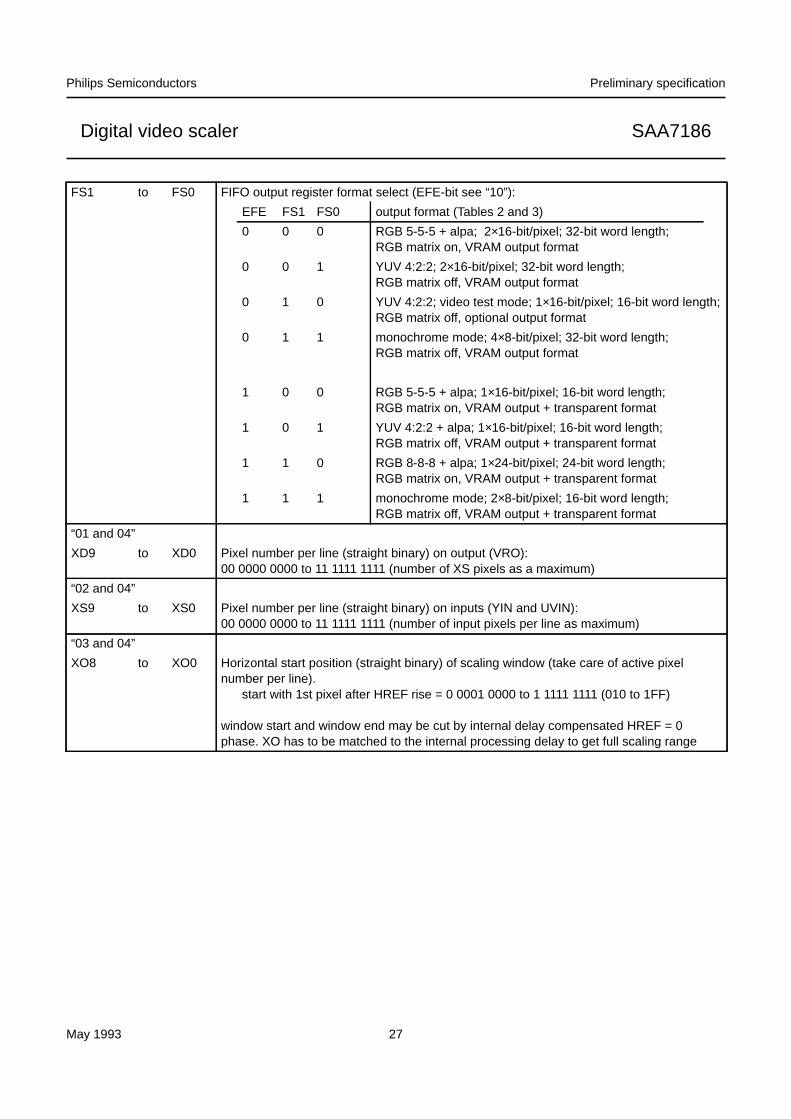
FS1 to FS0 FIFO output register format select (EFE-bit see “10”):
EFE FS1 FS0 output format (Tables 2 and 3)
0 0 0 RGB 5-5-5 + alpa; 2×16-bit/pixel; 32-bit word length;RGB matrix on, VRAM output format
0 0 1 YUV 4:2:2; 2×16-bit/pixel; 32-bit word length;RGB matrix off, VRAM output format
0 1 0 YUV 4:2:2; video test mode; 1×16-bit/pixel; 16-bit word length;RGB matrix off, optional output format
0 1 1 monochrome mode; 4×8-bit/pixel; 32-bit word length;RGB matrix off, VRAM output format
1 0 0 RGB 5-5-5 + alpa; 1×16-bit/pixel; 16-bit word length;RGB matrix on, VRAM output + transparent format
1 0 1 YUV 4:2:2 + alpa; 1×16-bit/pixel; 16-bit word length;RGB matrix off, VRAM output + transparent format
1 1 0 RGB 8-8-8 + alpa; 1×24-bit/pixel; 24-bit word length;RGB matrix on, VRAM output + transparent format
1 1 1 monochrome mode; 2×8-bit/pixel; 16-bit word length;RGB matrix off, VRAM output + transparent format
“01 and 04”
XD9 to XD0 Pixel number per line (straight binary) on output (VRO):00 0000 0000 to 11 1111 1111 (number of XS pixels as a maximum)
“02 and 04”
XS9 to XS0 Pixel number per line (straight binary) on inputs (YIN and UVIN):00 0000 0000 to 11 1111 1111 (number of input pixels per line as maximum)
“03 and 04”
XO8 to XO0 Horizontal start position (straight binary) of scaling window (take care of active pixelnumber per line).
start with 1st pixel after HREF rise = 0 0001 0000 to 1 1111 1111 (010 to 1FF)
window start and window end may be cut by internal delay compensated HREF = 0phase. XO has to be matched to the internal processing delay to get full scaling range
May 1993 28
Philips Semiconductors Preliminary specification
Digital video scaler SAA7186
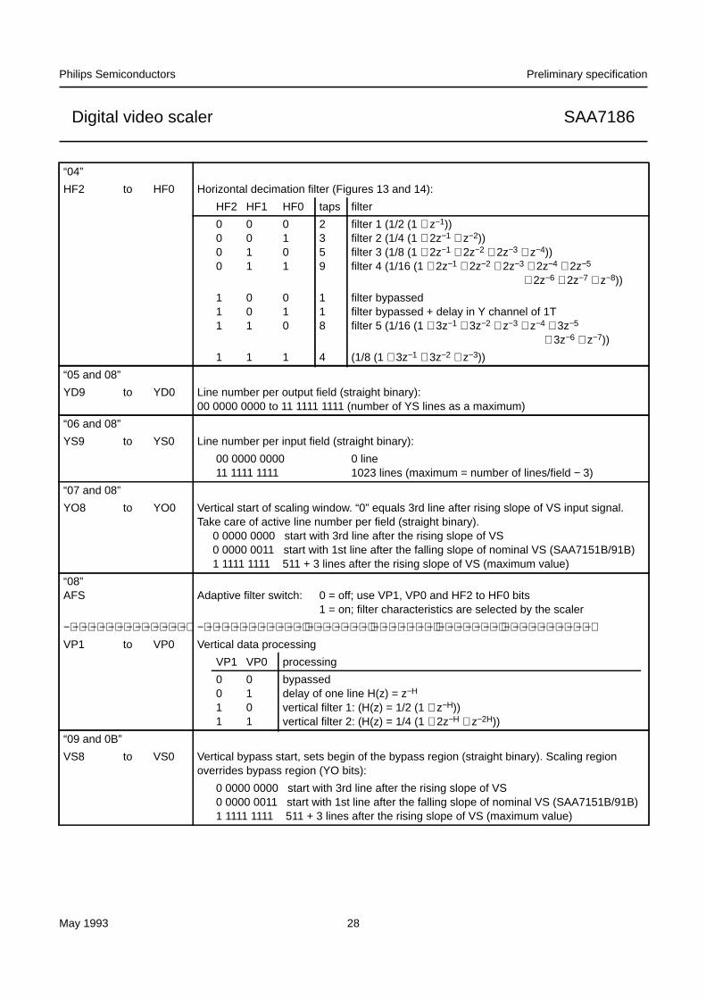
“04”
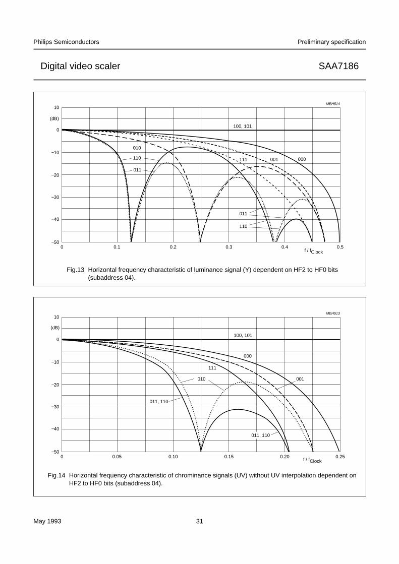
HF2 to HF0 Horizontal decimation filter (Figures 13 and 14):
HF2 HF1 HF0 taps filter
0000
0011
0101
2359
filter 1 (1/2 (1 + z−1))filter 2 (1/4 (1 + 2z−1 + z−2))filter 3 (1/8 (1 + 2z−1 + 2z−2 + 2z−3 + z−4))filter 4 (1/16 (1 + 2z−1 + 2z−2 + 2z−3 + 2z−4 + 2z−5
+ 2z−6 + 2z−7 + z−8))
111
001
010
118
filter bypassedfilter bypassed + delay in Y channel of 1Tfilter 5 (1/16 (1 + 3z−1 + 3z−2 + z−3 + z−4 + 3z−5
+ 3z−6 + z−7))
1 1 1 4 (1/8 (1 + 3z−1 + 3z−2 + z−3))
“05 and 08”
YD9 to YD0 Line number per output field (straight binary):00 0000 0000 to 11 1111 1111 (number of YS lines as a maximum)
“06 and 08”
YS9 to YS0 Line number per input field (straight binary):
00 0000 000011 1111 1111
0 line1023 lines (maximum = number of lines/field − 3)
“07 and 08”
YO8 to YO0 Vertical start of scaling window. “0” equals 3rd line after rising slope of VS input signal.Take care of active line number per field (straight binary).
0 0000 0000 start with 3rd line after the rising slope of VS0 0000 0011 start with 1st line after the falling slope of nominal VS (SAA7151B/91B)1 1111 1111 511 + 3 lines after the rising slope of VS (maximum value)
“08”AFS Adaptive filter switch: 0 = off; use VP1, VP0 and HF2 to HF0 bits
1 = on; filter characteristics are selected by the scaler
−⋅−⋅−⋅−⋅−⋅−⋅−⋅−⋅−⋅−⋅−⋅−⋅−⋅−⋅ −⋅−⋅−⋅−⋅−⋅−⋅−⋅−⋅−⋅−⋅−⋅−⋅⋅−⋅−⋅−⋅−⋅−⋅−⋅−⋅⋅−⋅−⋅−⋅−⋅−⋅−⋅−⋅⋅−⋅−⋅−⋅−⋅−⋅−⋅−⋅⋅−⋅−⋅−⋅−⋅−⋅−⋅−⋅−⋅−⋅−⋅VP1 to VP0 Vertical data processing
VP1 VP0 processing
0011
0101
bypasseddelay of one line H(z) = z−H
vertical filter 1: (H(z) = 1/2 (1 + z−H))vertical filter 2: (H(z) = 1/4 (1 + 2z−H + z−2H))
“09 and 0B”
VS8 to VS0 Vertical bypass start, sets begin of the bypass region (straight binary). Scaling regionoverrides bypass region (YO bits):
0 0000 0000 start with 3rd line after the rising slope of VS0 0000 0011 start with 1st line after the falling slope of nominal VS (SAA7151B/91B)1 1111 1111 511 + 3 lines after the rising slope of VS (maximum value)
May 1993 29
Philips Semiconductors Preliminary specification
Digital video scaler SAA7186
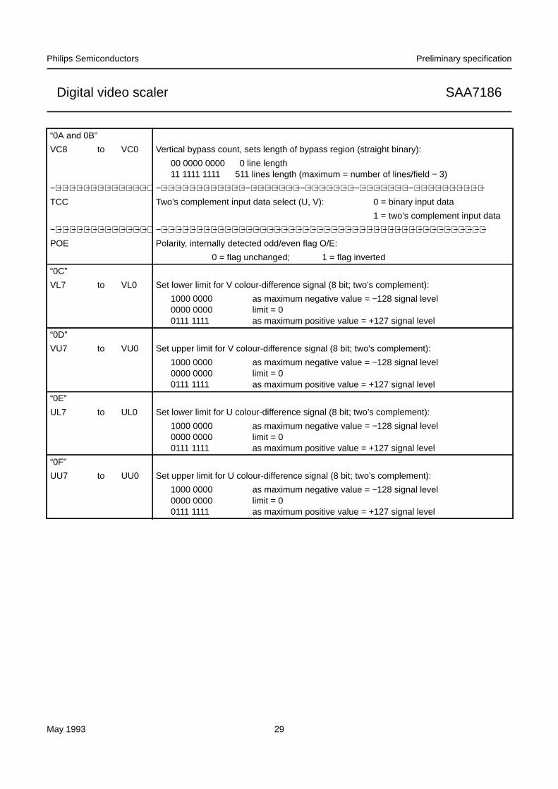
“0A and 0B”
VC8 to VC0 Vertical bypass count, sets length of bypass region (straight binary):
00 0000 0000 0 line length11 1111 1111 511 lines length (maximum = number of lines/field − 3)
−⋅−⋅−⋅−⋅−⋅−⋅−⋅−⋅−⋅−⋅−⋅−⋅−⋅−⋅ −⋅−⋅−⋅−⋅−⋅−⋅−⋅−⋅−⋅−⋅−⋅−⋅−−⋅−⋅−⋅−⋅−⋅−⋅−⋅−−⋅−⋅−⋅−⋅−⋅−⋅−⋅−−⋅−⋅−⋅−⋅−⋅−⋅−⋅−−⋅−⋅−⋅−⋅−⋅−⋅−⋅−⋅−⋅−⋅−TCC Two’s complement input data select (U, V): 0 = binary input data
1 = two’s complement input data
−⋅−⋅−⋅−⋅−⋅−⋅−⋅−⋅−⋅−⋅−⋅−⋅−⋅−⋅ −⋅−⋅−⋅−⋅−⋅−⋅−⋅−⋅−⋅−⋅−⋅−⋅−⋅−⋅−⋅−⋅−⋅−⋅−⋅−⋅−⋅−⋅−⋅−⋅−⋅−⋅−⋅−⋅−⋅−⋅−⋅−⋅−⋅−⋅−⋅−⋅−⋅−⋅−⋅−⋅−⋅−⋅−⋅−⋅−⋅−⋅−POE Polarity, internally detected odd/even flag O/E:
0 = flag unchanged; 1 = flag inverted
“0C”
VL7 to VL0 Set lower limit for V colour-difference signal (8 bit; two’s complement):
1000 00000000 00000111 1111
as maximum negative value = −128 signal levellimit = 0as maximum positive value = +127 signal level
“0D”
VU7 to VU0 Set upper limit for V colour-difference signal (8 bit; two’s complement):
1000 00000000 00000111 1111
as maximum negative value = −128 signal levellimit = 0as maximum positive value = +127 signal level
“0E”
UL7 to UL0 Set lower limit for U colour-difference signal (8 bit; two’s complement):
1000 00000000 00000111 1111
as maximum negative value = −128 signal levellimit = 0as maximum positive value = +127 signal level
“0F”
UU7 to UU0 Set upper limit for U colour-difference signal (8 bit; two’s complement):
1000 00000000 00000111 1111
as maximum negative value = −128 signal levellimit = 0as maximum positive value = +127 signal level

May 1993 30
Philips Semiconductors Preliminary specification
Digital video scaler SAA7186
“10”MCT Monochrome and two’s complement output data select:
0 = inverse greyscale luminance (if greyscale is selected by FS bits) or straightbinary U, V data output
1 = non-inverse monochrome luminance (if greyscale is selected by FS bits) ortwo’s complement U, V data output
−⋅−⋅−⋅−⋅−⋅−⋅−⋅−⋅−⋅−⋅−⋅−⋅−⋅−⋅ −⋅−⋅−⋅−⋅−⋅−⋅−⋅−⋅−⋅−⋅−−⋅−⋅−⋅−⋅−⋅−⋅−⋅−−⋅−⋅−⋅−⋅−⋅−⋅−⋅−−⋅−⋅−⋅−⋅−⋅−⋅−⋅−−⋅−⋅−⋅−⋅−⋅−⋅−⋅−⋅−⋅−⋅−⋅−⋅−QPL Line qualifier polarity flag : 0 = LNQ is active-LOW (pin 1 and on VRO1, pin 99);
1 = LNQ is active-HIGH
−⋅−⋅−⋅−⋅−⋅−⋅−⋅−⋅−⋅−⋅−⋅−⋅−⋅−⋅ −⋅−⋅−⋅−⋅−⋅−⋅−⋅−⋅−⋅−⋅−⋅−⋅−⋅−⋅−⋅−⋅−⋅−⋅−⋅−⋅−⋅−⋅−⋅−⋅−⋅−⋅−⋅−⋅−⋅−⋅−⋅−⋅−⋅−⋅−⋅−⋅−⋅−⋅−⋅−⋅−⋅−⋅−⋅−⋅−⋅−QPP Pixel qualifier polarity flag : 0 = PXQ is active-LOW (VRO0, pin 100);
1 = PXQ is active-HIGH
−⋅−⋅−⋅−⋅−⋅−⋅−⋅−⋅−⋅−⋅−⋅−⋅−⋅−⋅ −⋅−⋅−⋅−⋅−⋅−⋅−⋅−⋅−⋅−⋅−−⋅−⋅−⋅−⋅−⋅−⋅−⋅−−⋅−⋅−⋅−⋅−⋅−⋅−⋅−−⋅−⋅−⋅−⋅−⋅−⋅−⋅−−⋅−⋅−⋅−⋅−⋅−⋅−⋅−⋅−⋅−⋅−⋅−⋅−TTR Transparent data transfer: 0 = normal operation (VRAM protocol valid,)
1 = FIFO register transparent(output FIFO in shift register mode)
−⋅−⋅−⋅−⋅−⋅−⋅−⋅−⋅−⋅−⋅−⋅−⋅−⋅−⋅ −⋅−⋅−⋅−⋅−⋅−⋅−⋅−⋅−⋅−⋅−−⋅−⋅−⋅−⋅−⋅−⋅−⋅−−⋅−⋅−⋅−⋅−⋅−⋅−⋅−−⋅−⋅−⋅−⋅−⋅−⋅−⋅−−⋅−⋅−⋅−⋅−⋅−⋅−⋅−⋅−⋅−⋅−⋅−⋅−EFE Extended formats enable, FS-bits in subaddress “00”
May 1993 31
Philips Semiconductors Preliminary specification
Digital video scaler SAA7186
Fig.13 Horizontal frequency characteristic of luminance signal (Y) dependent on HF2 to HF0 bits(subaddress 04).
handbook, full pagewidth
0.5
10
−500 0.1 0.2
100, 101
000 001 111
011
011
110
010
110
0.3 0.4
−10
0
−40
−30
−20
MEH514
f / fClock
(dB)
handbook, full pagewidth
0.25
10
−500
f / fClock
011, 110
(dB)
0.05 0.10 0.15 0.20
−10
0
−40
−30
−20
MEH513
010 001
000
111
011, 110
100, 101
Fig.14 Horizontal frequency characteristic of chrominance signals (UV) without UV interpolation dependent onHF2 to HF0 bits (subaddress 04).

May 1993 32
Philips Semiconductors Preliminary specification
Digital video scaler SAA7186
10 LIMITING VALUESIn accordance with the Absolute Maximum Rating System (IEC 134).
Note
1. Equivalent to discharging a 100 pF capacitor through a 1.5 kΩ series resistor.
11 DC CHARACTERISTICSVDD1 to VDD8 = 4.5 to 5.5 V; Tamb = 0 to 70 °C unless otherwise specified.
SYMBOL PARAMETER MIN. MAX. UNIT
VDD supply voltage (pins 5, 14, 26, 40, 55, 67, 76 and 91) −0.5 6.5 V
VI DC input voltage on all pins −0.5 VDD V
IDD supply current (pins 5, 14, 26, 40, 55, 67, 76 and 91) − 70 mA
Ptot total power dissipation 0 1 W
Tstg storage temperature range −65 150 °CTamb operating ambient temperature range 0 70 °CVESD electrostatic handling(1) for all pins − ±2000 V
SYMBOL PARAMETER CONDITIONS MIN. TYP. MAX. UNIT
VDD supply voltage range (pins 5, 14, 26, 40,55, 67, 76 and 91)
4.5 5 5.5 V
IP total supply current (IDD1 + IDD2 + IDD3 +IDD4 + IDD5 + IDD6 + IDD7 + IDD8)
inputs LOW andoutputs without load
− 80 − mA
Data and control inputs
VI L input voltage LOW −0.5 − 0.8 V
VI H input voltage HIGH 2.0 − VDD+0.5 V
ILI input leakage current VI L = 0 − − 10 µA
CI input capacitance data − − 8 pF
clocks − − 10 pF
Data and control outputs
VO L output voltage LOW note 1 − − 0.6 V
VO H output voltage HIGH note 1 2.4 − − V
3-state outputs
IO off high-impedance output current − − ±5 µA
CO high-impedance output capacitance − − 8 pF
I2C-bus, SDA and SCL (pins 44 and 45)
VI L input voltage LOW −0.5 − 1.5 V
VI H input voltage HIGH 3 − VDD+0.5 V
I44, 45 input current − − ±10 µA
IACK output current on pin 44 acknowledge 3 − − mA
VO L output voltage at acknowledge I44 = 3 mA − − 0.4 V
May 1993 33
Philips Semiconductors Preliminary specification
Digital video scaler SAA7186
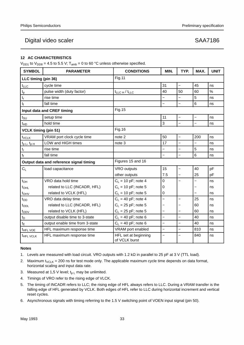
12 AC CHARACTERISTICSVDD1 to VDD8 = 4.5 to 5.5 V; Tamb = 0 to 60 °C unless otherwise specified.
Notes
1. Levels are measured with load circuit. VRO outputs with 1.2 kΩ in parallel to 25 pF at 3 V (TTL load).
2. Maximum tVCLK = 200 ns for test mode only. The applicable maximum cycle time depends on data format,horizontal scaling and input data rate.
3. Measured at 1,5 V level; tp L may be unlimited.
4. Timings of VRO refer to the rising edge of VLCK.
5. The timing of INCADR refers to LLC; the rising edge of HFL always refers to LLC. During a VRAM transfer is thefalling edge of HFL generated by VCLK. Both edges of HFL refer to LLC during horizontal increment and verticalreset cycles.
6. Asynchronous signals with timing referring to the 1.5 V switching point of VOEN input signal (pin 50).
SYMBOL PARAMETER CONDITIONS MIN. TYP. MAX. UNIT
LLC timing (pin 36) Fig.11
tLLC cycle time 31 − 45 ns
tp pulse width (duty factor) tLLC H / tLLC 40 50 60 %
tr rise time − − 5 ns
tf fall time − − 6 ns
Input data and CREF timing Fig.15
tSU setup time 11 − − ns
tHD hold time 3 − − ns
VCLK timing (pin 51) Fig.16
tVCLK VRAM port clock cycle time note 2 50 − 200 ns
tp L, tp H LOW and HIGH times note 3 17 − − ns
tr rise time − − 5 ns
tf fall time − − 6 ns
Output data and reference signal timing Figures 15 and 16
CL load capacitance VRO outputs 15 − 40 pF
other outputs 7.5 − 25 pF
tOH VRO data hold time CL = 10 pF; note 4 0 − − ns
tOHL related to LLC (INCADR, HFL) CL = 10 pF; note 5 0 − ns
tOHV related to VCLK (HFL) CL = 10 pF; note 5 0 − ns
tOD VRO data delay time CL = 40 pF; note 4 − − 25 ns
tODL related to LLC (INCADR, HFL) CL = 25 pF; note 5 − − 60 ns
tODV related to VCLK (HFL) CL = 25 pF; note 5 − − 60 ns
tD output disable time to 3-state CL = 40 pF; note 6 − − 40 ns
tE output enable time from 3-state CL = 40 pF; note 6 − − 40 ns
tHFL VOE HFL maximum response time VRAM port enabled − − 810 ns
tHFL VCLK HFL maximum response time HFL set at beginningof VCLK burst
− − 840 ns

May 1993 34
Philips Semiconductors Preliminary specification
Digital video scaler SAA7186
handbook, full pagewidth
MEH408-1
clock input LLC
t LLC H
t LLC
t f t r
2.4 V
1.5 V
0.6 V
input data
output HFLand INCADR
t SU t HD
t OHL
2.0 V
0.8 V
2.4 V
0.6 V
t ODL
not valid
not valid
2.0 V
0.8 Vinputs CREF
t HDt SU
Fig.15 Data input timing (LLC).
May 1993 35
Philips Semiconductors Preliminary specification
Digital video scaler SAA7186
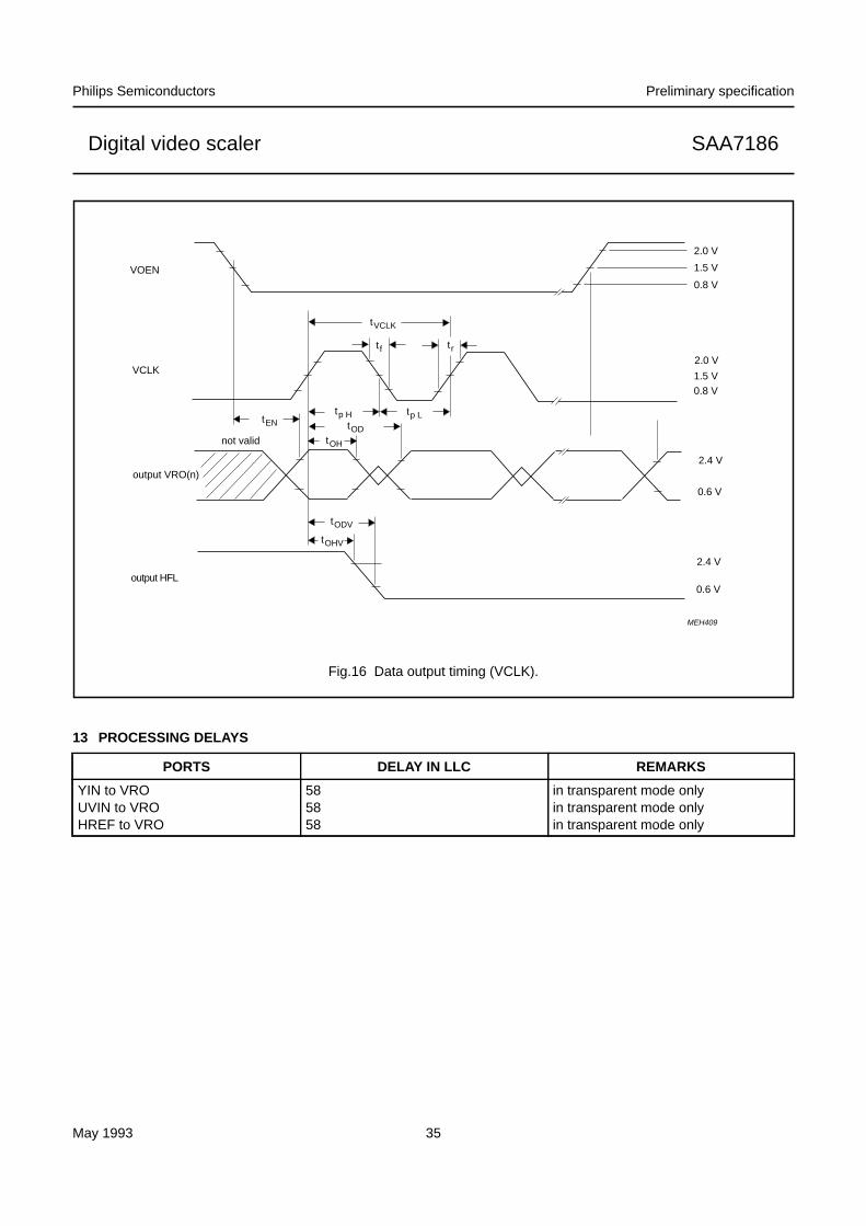
13 PROCESSING DELAYS
PORTS DELAY IN LLC REMARKS
YIN to VROUVIN to VROHREF to VRO
585858
in transparent mode onlyin transparent mode onlyin transparent mode only
handbook, full pagewidth
MEH409
VOEN
2.0 V
1.5 V
0.8 V
VCLK
output VRO(n)
2.0 V
0.8 V
2.4 V
0.6 V
not valid
0.6 V
2.4 V
output HFL
tf tr
tVCLK
tp Ltp HtEN tODtOH
tODV
tOHV
1.5 V
Fig.16 Data output timing (VCLK).
May 1993 36
Philips Semiconductors Preliminary specification
Digital video scaler SAA7186
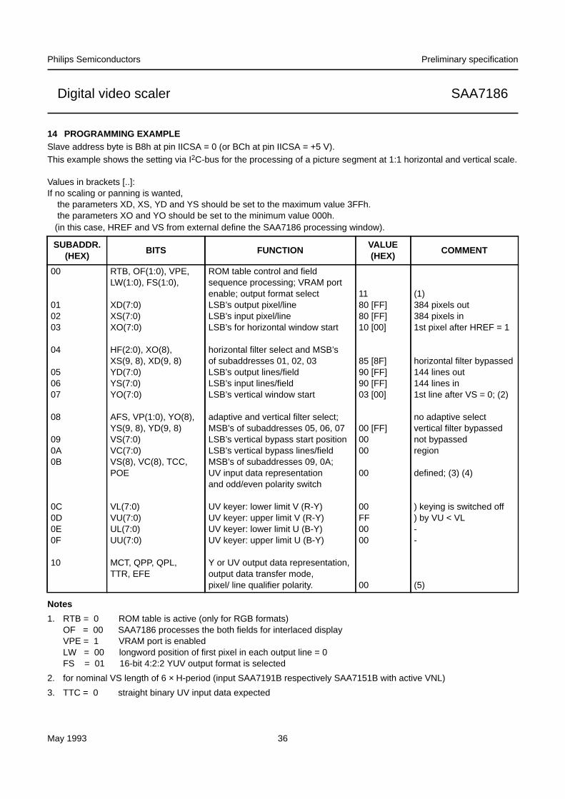
14 PROGRAMMING EXAMPLESlave address byte is B8h at pin IICSA = 0 (or BCh at pin IICSA = +5 V).This example shows the setting via I2C-bus for the processing of a picture segment at 1:1 horizontal and vertical scale.
Values in brackets [..]:If no scaling or panning is wanted,
the parameters XD, XS, YD and YS should be set to the maximum value 3FFh.the parameters XO and YO should be set to the minimum value 000h.
(in this case, HREF and VS from external define the SAA7186 processing window).
Notes
1. RTB = 0 ROM table is active (only for RGB formats)OF = 00 SAA7186 processes the both fields for interlaced displayVPE = 1 VRAM port is enabledLW = 00 longword position of first pixel in each output line = 0FS = 01 16-bit 4:2:2 YUV output format is selected
2. for nominal VS length of 6 × H-period (input SAA7191B respectively SAA7151B with active VNL)
3. TTC = 0 straight binary UV input data expected
SUBADDR.(HEX)
BITS FUNCTIONVALUE(HEX)
COMMENT
00
010203
04
050607
08
090A0B
0C0D0E0F
10
RTB, OF(1:0), VPE,LW(1:0), FS(1:0),
XD(7:0)XS(7:0)XO(7:0)
HF(2:0), XO(8),XS(9, 8), XD(9, 8)YD(7:0)YS(7:0)YO(7:0)
AFS, VP(1:0), YO(8),YS(9, 8), YD(9, 8)VS(7:0)VC(7:0)VS(8), VC(8), TCC,POE
VL(7:0)VU(7:0)UL(7:0)UU(7:0)
MCT, QPP, QPL,TTR, EFE
ROM table control and fieldsequence processing; VRAM portenable; output format selectLSB’s output pixel/lineLSB’s input pixel/lineLSB’s for horizontal window start
horizontal filter select and MSB’sof subaddresses 01, 02, 03LSB’s output lines/fieldLSB’s input lines/fieldLSB’s vertical window start
adaptive and vertical filter select;MSB’s of subaddresses 05, 06, 07LSB’s vertical bypass start positionLSB’s vertical bypass lines/fieldMSB’s of subaddresses 09, 0A;UV input data representationand odd/even polarity switch
UV keyer: lower limit V (R-Y)UV keyer: upper limit V (R-Y)UV keyer: lower limit U (B-Y)UV keyer: upper limit U (B-Y)
Y or UV output data representation,output data transfer mode,pixel/ line qualifier polarity.
1180 [FF]80 [FF]10 [00]
85 [8F]90 [FF]90 [FF]03 [00]
00 [FF]0000
00
00FF0000
00
(1)384 pixels out384 pixels in1st pixel after HREF = 1
horizontal filter bypassed144 lines out144 lines in1st line after VS = 0; (2)
no adaptive selectvertical filter bypassednot bypassedregion
defined; (3) (4)
) keying is switched off) by VU < VL--
(5)
May 1993 37
Philips Semiconductors Preliminary specification
Digital video scaler SAA7186
4. odd/even polarity unchanged - can be used to change the field sequence if phase relations between HREF and VSare not according to SAA7191B respectively SAA7151B specification
5. MCT = 0 when EFE, FS = 001h: UV output data are straight binaryQPP = 0 the pixel qualifier PXQ is “0”-active (if TTR, EFE = 1)QPL = 0 line qualifier LNQ is “0”-active (if TTR, EFE = 1)TTR = 0 VRAM port is set to data burst transferEFE = 0 32-bit longword formats selected.
May 1993 38
Philips Semiconductors Preliminary specification
Digital video scaler SAA7186
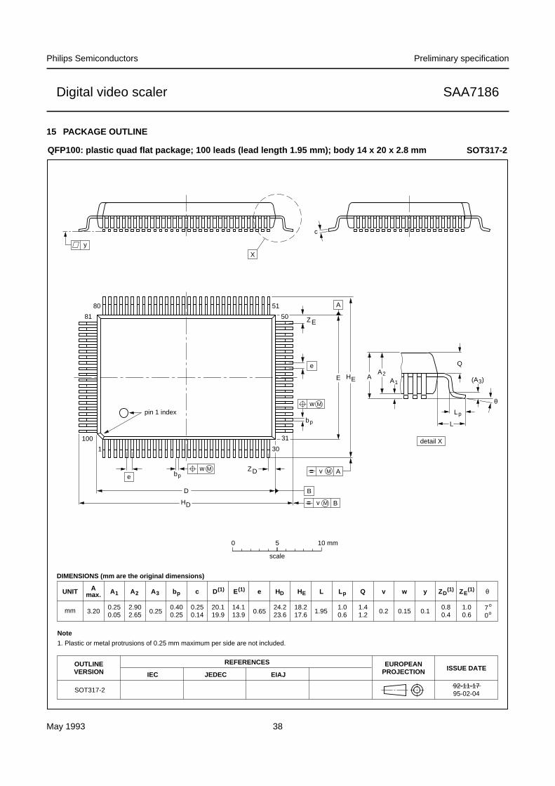
15 PACKAGE OUTLINE
UNIT A1 A2 A3 bp c E(1) e HE L Lp Q Zywv θ
REFERENCESOUTLINEVERSION
EUROPEANPROJECTION ISSUE DATE
IEC JEDEC EIAJ
mm 0.250.05
2.902.65 0.25
0.400.25
0.250.14
14.113.9 0.65
18.217.6
1.41.2
1.00.6
70
o
o0.15 0.10.21.95
DIMENSIONS (mm are the original dimensions)
Note
1. Plastic or metal protrusions of 0.25 mm maximum per side are not included.
1.00.6
SOT317-292-11-1795-02-04
D(1) (1)(1)
20.119.9
HD
24.223.6
EZ
0.80.4
D
e
θ
E A1A
Lp
Q
detail X
L
(A )3
B
30
c
bp
EHA2
D
ZD
A
ZE
e
v M A
1
100
81
80 51
50
31
pin 1 index
X
y
bp
DH v M B
w M
w M
0 5 10 mm
scale
QFP100: plastic quad flat package; 100 leads (lead length 1.95 mm); body 14 x 20 x 2.8 mm SOT317-2
Amax.
3.20

May 1993 39
Philips Semiconductors Preliminary specification
Digital video scaler SAA7186
16 SOLDERING
16.1 Introduction
There is no soldering method that is ideal for all ICpackages. Wave soldering is often preferred whenthrough-hole and surface mounted components are mixedon one printed-circuit board. However, wave soldering isnot always suitable for surface mounted ICs, or forprinted-circuits with high population densities. In thesesituations reflow soldering is often used.
This text gives a very brief insight to a complex technology.A more in-depth account of soldering ICs can be found inour “IC Package Databook” (order code 9398 652 90011).
16.2 Reflow soldering
Reflow soldering techniques are suitable for all QFPpackages.
The choice of heating method may be influenced by largerplastic QFP packages (44 leads, or more). If infrared orvapour phase heating is used and the large packages arenot absolutely dry (less than 0.1% moisture content byweight), vaporization of the small amount of moisture inthem can cause cracking of the plastic body. For moreinformation, refer to the Drypack chapter in our “QualityReference Handbook” (order code 9397 750 00192).
Reflow soldering requires solder paste (a suspension offine solder particles, flux and binding agent) to be appliedto the printed-circuit board by screen printing, stencilling orpressure-syringe dispensing before package placement.
Several techniques exist for reflowing; for example,thermal conduction by heated belt. Dwell times varybetween 50 and 300 seconds depending on heatingmethod. Typical reflow temperatures range from215 to 250 °C.
Preheating is necessary to dry the paste and evaporatethe binding agent. Preheating duration: 45 minutes at45 °C.
16.3 Wave soldering
Wave soldering is not recommended for QFP packages.This is because of the likelihood of solder bridging due toclosely-spaced leads and the possibility of incompletesolder penetration in multi-lead devices.
If wave soldering cannot be avoided, the followingconditions must be observed:
• A double-wave (a turbulent wave with high upwardpressure followed by a smooth laminar wave)soldering technique should be used.
• The footprint must be at an angle of 45 ° to the boarddirection and must incorporate solder thievesdownstream and at the side corners.
Even with these conditions, do not consider wavesoldering the following packages: QFP52 (SOT379-1),QFP100 (SOT317-1), QFP100 (SOT317-2),QFP100 (SOT382-1) or QFP160 (SOT322-1).
During placement and before soldering, the package mustbe fixed with a droplet of adhesive. The adhesive can beapplied by screen printing, pin transfer or syringedispensing. The package can be soldered after theadhesive is cured.
Maximum permissible solder temperature is 260 °C, andmaximum duration of package immersion in solder is10 seconds, if cooled to less than 150 °C within6 seconds. Typical dwell time is 4 seconds at 250 °C.
A mildly-activated flux will eliminate the need for removalof corrosive residues in most applications.
16.4 Repairing soldered joints
Fix the component by first soldering two diagonally-opposite end leads. Use only a low voltage soldering iron(less than 24 V) applied to the flat part of the lead. Contacttime must be limited to 10 seconds at up to 300 °C. Whenusing a dedicated tool, all other leads can be soldered inone operation within 2 to 5 seconds between270 and 320 °C.

May 1993 40
Philips Semiconductors Preliminary specification
Digital video scaler SAA7186
17 DEFINITIONS
18 LIFE SUPPORT APPLICATIONS
These products are not designed for use in life support appliances, devices, or systems where malfunction of theseproducts can reasonably be expected to result in personal injury. Philips customers using or selling these products foruse in such applications do so at their own risk and agree to fully indemnify Philips for any damages resulting from suchimproper use or sale.
19 PURCHASE OF PHILIPS I2C COMPONENTS
Data sheet status
Objective specification This data sheet contains target or goal specifications for product development.
Preliminary specification This data sheet contains preliminary data; supplementary data may be published later.
Product specification This data sheet contains final product specifications.
Limiting values
Limiting values given are in accordance with the Absolute Maximum Rating System (IEC 134). Stress above one ormore of the limiting values may cause permanent damage to the device. These are stress ratings only and operationof the device at these or at any other conditions above those given in the Characteristics sections of the specificationis not implied. Exposure to limiting values for extended periods may affect device reliability.
Application information
Where application information is given, it is advisory and does not form part of the specification.
Purchase of Philips I2C components conveys a license under the Philips’ I2C patent to use thecomponents in the I2C system provided the system conforms to the I2C specification defined byPhilips. This specification can be ordered using the code 9398 393 40011.

May 1993 41
Philips Semiconductors Preliminary specification
Digital video scaler SAA7186
NOTES

May 1993 42
Philips Semiconductors Preliminary specification
Digital video scaler SAA7186
NOTES
May 1993 43
Philips Semiconductors Preliminary specification
Digital video scaler SAA7186
NOTES

Internet: http://www.semiconductors.philips.com
Philips Semiconductors – a worldwide company
© Philips Electronics N.V. 1997 SCA54
All rights are reserved. Reproduction in whole or in part is prohibited without the prior written consent of the copyright owner.
The information presented in this document does not form part of any quotation or contract, is believed to be accurate and reliable and may be changedwithout notice. No liability will be accepted by the publisher for any consequence of its use. Publication thereof does not convey nor imply any licenseunder patent- or other industrial or intellectual property rights.
Netherlands: Postbus 90050, 5600 PB EINDHOVEN, Bldg. VB,Tel. +31 40 27 82785, Fax. +31 40 27 88399
New Zealand: 2 Wagener Place, C.P.O. Box 1041, AUCKLAND,Tel. +64 9 849 4160, Fax. +64 9 849 7811
Norway: Box 1, Manglerud 0612, OSLO,Tel. +47 22 74 8000, Fax. +47 22 74 8341
Philippines: Philips Semiconductors Philippines Inc.,106 Valero St. Salcedo Village, P.O. Box 2108 MCC, MAKATI,Metro MANILA, Tel. +63 2 816 6380, Fax. +63 2 817 3474
Poland: Ul. Lukiska 10, PL 04-123 WARSZAWA,Tel. +48 22 612 2831, Fax. +48 22 612 2327
Portugal: see Spain
Romania: see Italy
Russia: Philips Russia, Ul. Usatcheva 35A, 119048 MOSCOW,Tel. +7 095 755 6918, Fax. +7 095 755 6919
Singapore: Lorong 1, Toa Payoh, SINGAPORE 1231,Tel. +65 350 2538, Fax. +65 251 6500
Slovakia: see Austria
Slovenia: see Italy
South Africa: S.A. PHILIPS Pty Ltd., 195-215 Main Road Martindale,2092 JOHANNESBURG, P.O. Box 7430 Johannesburg 2000,Tel. +27 11 470 5911, Fax. +27 11 470 5494
South America: Rua do Rocio 220, 5th floor, Suite 51,04552-903 São Paulo, SÃO PAULO - SP, Brazil,Tel. +55 11 821 2333, Fax. +55 11 829 1849
Spain: Balmes 22, 08007 BARCELONA,Tel. +34 3 301 6312, Fax. +34 3 301 4107
Sweden: Kottbygatan 7, Akalla, S-16485 STOCKHOLM,Tel. +46 8 632 2000, Fax. +46 8 632 2745
Switzerland: Allmendstrasse 140, CH-8027 ZÜRICH,Tel. +41 1 488 2686, Fax. +41 1 481 7730
Taiwan: Philips Semiconductors, 6F, No. 96, Chien Kuo N. Rd., Sec. 1,TAIPEI, Taiwan Tel. +886 2 2134 2865, Fax. +886 2 2134 2874
Thailand: PHILIPS ELECTRONICS (THAILAND) Ltd.,209/2 Sanpavuth-Bangna Road Prakanong, BANGKOK 10260,Tel. +66 2 745 4090, Fax. +66 2 398 0793
Turkey: Talatpasa Cad. No. 5, 80640 GÜLTEPE/ISTANBUL,Tel. +90 212 279 2770, Fax. +90 212 282 6707
Ukraine : PHILIPS UKRAINE, 4 Patrice Lumumba str., Building B, Floor 7,252042 KIEV, Tel. +380 44 264 2776, Fax. +380 44 268 0461
United Kingdom: Philips Semiconductors Ltd., 276 Bath Road, Hayes,MIDDLESEX UB3 5BX, Tel. +44 181 730 5000, Fax. +44 181 754 8421
United States: 811 East Arques Avenue, SUNNYVALE, CA 94088-3409,Tel. +1 800 234 7381
Uruguay: see South America
Vietnam: see Singapore
Yugoslavia: PHILIPS, Trg N. Pasica 5/v, 11000 BEOGRAD,Tel. +381 11 625 344, Fax.+381 11 635 777
For all other countries apply to: Philips Semiconductors, Marketing & Sales Communications,Building BE-p, P.O. Box 218, 5600 MD EINDHOVEN, The Netherlands, Fax. +31 40 27 24825
Argentina: see South America
Australia: 34 Waterloo Road, NORTH RYDE, NSW 2113,Tel. +61 2 9805 4455, Fax. +61 2 9805 4466
Austria: Computerstr. 6, A-1101 WIEN, P.O. Box 213,Tel. +43 1 60 101, Fax. +43 1 60 101 1210
Belarus: Hotel Minsk Business Center, Bld. 3, r. 1211, Volodarski Str. 6,220050 MINSK, Tel. +375 172 200 733, Fax. +375 172 200 773
Belgium: see The Netherlands
Brazil: see South America
Bulgaria: Philips Bulgaria Ltd., Energoproject, 15th floor,51 James Bourchier Blvd., 1407 SOFIA,Tel. +359 2 689 211, Fax. +359 2 689 102
Canada: PHILIPS SEMICONDUCTORS/COMPONENTS,Tel. +1 800 234 7381
China/Hong Kong: 501 Hong Kong Industrial Technology Centre,72 Tat Chee Avenue, Kowloon Tong, HONG KONG,Tel. +852 2319 7888, Fax. +852 2319 7700
Colombia: see South America
Czech Republic: see Austria
Denmark: Prags Boulevard 80, PB 1919, DK-2300 COPENHAGEN S,Tel. +45 32 88 2636, Fax. +45 31 57 0044
Finland: Sinikalliontie 3, FIN-02630 ESPOO,Tel. +358 9 615800, Fax. +358 9 61580920
France: 4 Rue du Port-aux-Vins, BP317, 92156 SURESNES Cedex,Tel. +33 1 40 99 6161, Fax. +33 1 40 99 6427
Germany: Hammerbrookstraße 69, D-20097 HAMBURG,Tel. +49 40 23 53 60, Fax. +49 40 23 536 300
Greece: No. 15, 25th March Street, GR 17778 TAVROS/ATHENS,Tel. +30 1 4894 339/239, Fax. +30 1 4814 240
Hungary: see Austria
India: Philips INDIA Ltd, Shivsagar Estate, A Block, Dr. Annie Besant Rd.Worli, MUMBAI 400 018, Tel. +91 22 4938 541, Fax. +91 22 4938 722
Indonesia: see Singapore
Ireland: Newstead, Clonskeagh, DUBLIN 14,Tel. +353 1 7640 000, Fax. +353 1 7640 200
Israel: RAPAC Electronics, 7 Kehilat Saloniki St, PO Box 18053,TEL AVIV 61180, Tel. +972 3 645 0444, Fax. +972 3 649 1007
Italy: PHILIPS SEMICONDUCTORS, Piazza IV Novembre 3,20124 MILANO, Tel. +39 2 6752 2531, Fax. +39 2 6752 2557
Japan: Philips Bldg 13-37, Kohnan 2-chome, Minato-ku, TOKYO 108,Tel. +81 3 3740 5130, Fax. +81 3 3740 5077
Korea: Philips House, 260-199 Itaewon-dong, Yongsan-ku, SEOUL,Tel. +82 2 709 1412, Fax. +82 2 709 1415
Malaysia: No. 76 Jalan Universiti, 46200 PETALING JAYA, SELANGOR,Tel. +60 3 750 5214, Fax. +60 3 757 4880
Mexico: 5900 Gateway East, Suite 200, EL PASO, TEXAS 79905,Tel. +9-5 800 234 7381
Middle East: see Italy
Printed in The Netherlands 657027/00/01/pp44 Date of release: May 1993 Document order number: 9397 750 02436