data-level parallelism - stony brooknhonarmand/courses/fa15/cse610/... · –data parallelism:...
TRANSCRIPT

Fall 2015 :: CSE 610 – Parallel Computer Architectures
Data-Level Parallelism
Nima Honarmand

Fall 2015 :: CSE 610 – Parallel Computer Architectures
Overview
• Data Parallelism vs. Control Parallelism– Data Parallelism: parallelism arises from executing essentially
the same code on a large number of objects
– Control Parallelism: parallelism arises from executing different threads of control concurrently
• Hypothesis: applications that use massively parallel machines will mostly exploit data parallelism
– Common in the Scientific Computing domain
• DLP originally linked with SIMD machines; now SIMT is more common
– SIMD: Single Instruction Multiple Data
– SIMT: Single Instruction Multiple Threads

Fall 2015 :: CSE 610 – Parallel Computer Architectures
Overview
• Many incarnations of DLP architectures over decades– Old vector processors
• Cray processors: Cray-1, Cray-2, …, Cray X1
– SIMD extensions• Intel SSE and AVX units
• Alpha Tarantula (didn’t see light of day )
– Old massively parallel computers• Connection Machines
• MasPar machines
– Modern GPUs• NVIDIA, AMD, Qualcomm, …
• Focus of throughput rather than latency
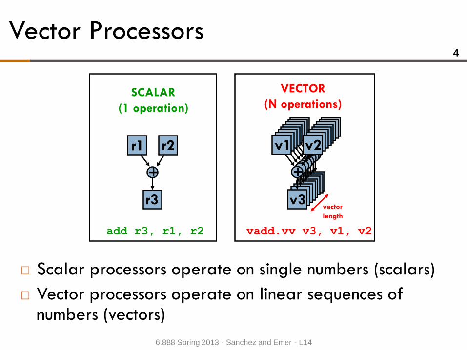
Vector Processors
Scalar processors operate on single numbers (scalars)
Vector processors operate on linear sequences of numbers (vectors)
+
r1 r2
r3
add r3, r1, r2
SCALAR
(1 operation)
v1 v2
v3
+
vector
length
vadd.vv v3, v1, v2
VECTOR
(N operations)
4
6.888 Spring 2013 - Sanchez and Emer - L14

What’s in a Vector Processor?
A scalar processor (e.g. a MIPS processor)
Scalar register file (32 registers)
Scalar functional units (arithmetic, load/store, etc)
A vector register file (a 2D register array)
Each register is an array of elements
E.g. 32 registers with 32 64-bit elements per register
MVL = maximum vector length = max # of elements per register
A set of vector functional units
Integer, FP, load/store, etc
Some times vector and scalar units are combined (share ALUs)
5
6.888 Spring 2013 - Sanchez and Emer - L14

Example of Simple
Vector Processor 6
6.888 Spring 2013 - Sanchez and Emer - L14

Basic Vector ISA
Instr. Operands Operation Comment
VADD.VV V1,V2,V3 V1=V2+V3 vector + vector
VADD.SV V1,R0,V2 V1=R0+V2 scalar + vector
VMUL.VV V1,V2,V3 V1=V2*V3 vector x vector
VMUL.SV V1,R0,V2 V1=R0*V2 scalar x vector
VLD V1,R1 V1=M[R1...R1+63] load, stride=1
VLDS V1,R1,R2 V1=M[R1…R1+63*R2] load, stride=R2
VLDX V1,R1,V2 V1=M[R1+V2i,i=0..63] indexed("gather")
VST V1,R1 M[R1...R1+63]=V1 store, stride=1
VSTS V1,R1,R2 V1=M[R1...R1+63*R2] store, stride=R2
VSTX V1,R1,V2 V1=M[R1+V2i,i=0..63] indexed(“scatter")
+ regular scalar instructions…
7
6.888 Spring 2013 - Sanchez and Emer - L14
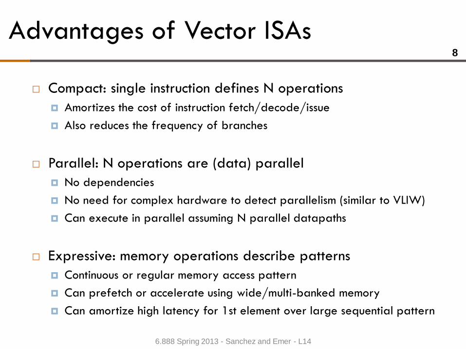
Advantages of Vector ISAs
Compact: single instruction defines N operations
Amortizes the cost of instruction fetch/decode/issue
Also reduces the frequency of branches
Parallel: N operations are (data) parallel
No dependencies
No need for complex hardware to detect parallelism (similar to VLIW)
Can execute in parallel assuming N parallel datapaths
Expressive: memory operations describe patterns
Continuous or regular memory access pattern
Can prefetch or accelerate using wide/multi-banked memory
Can amortize high latency for 1st element over large sequential pattern
8
6.888 Spring 2013 - Sanchez and Emer - L14

Vector Length (VL)9
Basic: Fixed vector length (typical in narrow SIMD)
Is this efficient for wide SIMD (e.g., 32-wide vectors)?
Vector-length (VL) register: Control the length of any vector operation,
including vector loads and stores
e.g. vadd.vv with VL=10 for (i=0; i<10; i++) V1[i]=V2[i]+V3[i]
VL can be set up to MVL (e.g., 32)
How to do vectors > MVL?
What if VL is unknown at compile time?
6.888 Spring 2013 - Sanchez and Emer - L14

Optimization 1: Chaining
Suppose the following code with VL=32:
vmul.vv V1,V2,V3
vadd.vv V4,V1,V5 # very long RAW hazard
Chaining
V1 is not a single entity but a group of individual elements
Pipeline forwarding can work on an element basis
Flexible chaining: allow vector to chain to any other active vector
operation => more read/write ports
vadd
vmul vadd
vmul
Unchained
Chained
10
6.888 Spring 2013 - Sanchez and Emer - L14

Optimization 2: Multiple Lanes
Modular, scalable design
Elements for each vector register interleaved across the lanes
Each lane receives identical control
Multiple element operations executed per cycle
No need for inter-lane communication for most vector instructions
To/From Memory System
Pipelined
Datapath
Functional
Unit
Lane
Vector Reg.
PartitionElements Elements Elements Elements
11
6.888 Spring 2013 - Sanchez and Emer - L14

Chaining & Multi-lane Example
VL=16, 4 lanes,
2 FUs, 1 LSU
chaining -> 12 ops/cycle
Just 1 new
instruction
issued per cycle
!!!!
vld
vmul.vv
vadd.vv
addu
vld
vmul.vv
vadd.vv
addu
LSU FU0 FU1Scalar
Time
Element Operations: Instr. Issue:
12
6.888 Spring 2013 - Sanchez and Emer - L14

Optimization 3: Conditional Execution
Suppose you want to vectorize this:
for (i=0; i<N; i++) if (A[i]!= B[i]) A[i] -= B[i];
Solution: Vector conditional execution (predication)
Add vector flag registers with single-bit elements (masks)
Use a vector compare to set the a flag register
Use flag register as mask control for the vector sub
Add executed only for vector elements with corresponding flag element set
Vector code
vld V1, Ra
vld V2, Rb
vcmp.neq.vv M0, V1, V2 # vector compare
vsub.vv V3, V2, V1, M0 # conditional vadd
vst V3, Ra
13
6.888 Spring 2013 - Sanchez and Emer - L14

SIMD: Intel Xeon Phi (Knights Corner)
A multi-core chip with x86-based vector processors
Ring interconnect, private L2 caches, coherent
Targeting the HPC market
Goal: high GFLOPS, GFLOPS/Watt
PCIe
Client
Logic
Core
L2
Core
L2
Core
L2
Core
L2
TD TD TD TD
Core
L2
Core
L2
Core
L2
Core
L2
TDTDTDTDGDDR MC
GDDR MC
GDDR MC
GDDR MC
14
6.888 Spring 2013 - Sanchez and Emer - L14

Xeon Phi Core Design
4-way threaded + vector processing
In-order (why?), short pipeline
Vector ISA: 32 vector registers (512b), 8 mask registers, scatter/gather
L2 Ctl
L1 TLB
and 32KB
Code Cache
T0 IP
4 Threads
In-Order
TLB Miss
Code Cache Miss
Decode uCode
16B/Cycle (2 IPC)
Pipe 0
X87 RF Scalar RF
X87 ALU 0 ALU 1
VPU RF
VPU
512b SIMD
Pipe 1
TLB Miss
Handler
L2 TLB
T1 IP
T2 IP
T3 IP
L1 TLB and 32KB Data CacheDCache Miss
TLB Miss
To On-Die Interconnect
HWP
Core
512KB
L2 Cache
PPF PF D0 D1 D2 E WB
15
6.888 Spring 2013 - Sanchez and Emer - L14

Fall 2015 :: CSE 610 – Parallel Computer Architectures
An Old Massively Parallel Computer:Connection Machine
• Originally intended for AI applications, later used for scientific computing
• CM-2 major components– Parallel Processing Unit (PPU)
• 16-64K bit-serial processing elements (PEs), each with 8KB of memory
• 20us for a 32-bit add → 3000 MIPS with 64K PEs
• Optional FPUs, 1 shared by 32 PEs
• Hypercube interconnect between PEs with support for combining operations
– 1-4 instruction sequencers

Fall 2015 :: CSE 610 – Parallel Computer Architectures
The Connection Machine (CM-2)
• 1-4 Front-End Computers– PPU was a peripheral
• Sophisticated I/O system– 256-bit wide I/O channel for
every 8K PEs– Data vault (39 disks, data +
ECC) for high-performance disk I/O
– Graphics support
• With 4 sequencers, a CM viewed as 4 independent smaller CMs

Fall 2015 :: CSE 610 – Parallel Computer Architectures
CM-2 ISA• Notion of virtual processors (VPs)
– VPs are independent of # of PEs in the machine– If VPs > PEs, then multiple VPs mapped to each PE
• System transparently splits memory per PE, does routing, etc.
• Notion of current context– A context flag in each PE identifies those participating in
computation• Used to execute conditional statements
• A very rich vector instruction set– Instructions mostly memory-to-memory– Standard set of scalar operations– Intra-PE vector instructions (vector within each PE)– Inter-PE vector instructions (each PE has one element of the vector)
• Global reductions, regular scans, segmented scans

Fall 2015 :: CSE 610 – Parallel Computer Architectures
Example of CM-2 Vector Insts
• global-s-add: reduction operator to return sum of all elements in a vector
• s-add-scan: parallel-prefix operation, replacing each vector item with sum of all items preceding it
• segmented-s-add-scan: parallel-prefix done on segments of an array

Fall 2015 :: CSE 610 – Parallel Computer Architectures
Inter-PE Communication in CM-2
• Underlying topology is 2-ary 12-cube– A general router: all PEs may concurrently send/receive
messages to/from other PEs
• Can impose a simpler grid (256-ary 2-cube or 16-ary 4-cube) on top of it for fast local communication
• Global communication– Fetch/store: assume only one PE storing to any given destn
– Get/send: multiple PEs may request from or send to a given dstn
• Network does combining
• E.g., send-with-s-max: only max value stored at destn

Fall 2015 :: CSE 610 – Parallel Computer Architectures
Graphics Processing Unit (GPU)
• An architecture for compute-intensive, highly data-parallel computation
– exactly what graphics rendering is about– Transistors can be devoted to data processing rather than
data caching and flow control
• The fast-growing video game industry exerts strong economic pressure that forces constant innovation
DRAM
Cache
ALUControl
ALU
ALU
ALU
DRAM
CPU GPU

Fall 2015 :: CSE 610 – Parallel Computer Architectures
Data Parallelism in GPUs
• GPUs take advantage of massive DLP to provide very high FLOP rates
– More than 1 Tera DP FLOP in NVIDIA GK110
• “SIMT” execution model– Single instruction multiple threads– Trying to distinguish itself from both “vectors” and “SIMD”– A key difference: better support for conditional control flow
• Program it with CUDA or OpenCL– Extensions to C– Perform a “shader task” (a snippet of scalar computation) over
many elements– Internally, GPU uses scatter/gather and vector-mask like
operations

Fall 2015 :: CSE 610 – Parallel Computer Architectures
Context: History of Programming GPUs
• “GPGPU”– Originally could only perform “shader” computations on images– So, programmers started using this framework for computation– Puzzle to work around the limitations, unlock the raw potential
• As GPU designers notice this trend…– Hardware provided more “hooks” for computation– Provided some limited software tools
• GPU designs are now fully embracing compute– More programmability features in each generation– Industrial-strength tools, documentation, tutorials, etc.– Can be used for in-game physics, etc.– A major initiative to push GPUs beyond graphics (HPC)


Fall 2015 :: CSE 610 – Parallel Computer Architectures
Latency Hiding with “Thread Warps”
• Warp: A set of threads that execute the same instruction (on different data elements)
• Fine-grained multithreading– One instruction per thread in
pipeline at a time (No branch prediction)
– Interleave warp execution to hide latencies
• Register values of all threads stay in register file
• No OS context switching
• Memory latency hiding– Graphics has millions of pixels
Decode
RF
RF
RF
ALU
ALU
ALU
D-Cache
Thread Warp 6
Thread Warp 1Thread Warp 2DataAll Hit?
Miss?
Warps accessingmemory hierarchy
Thread Warp 3Thread Warp 8
Writeback
Warps availablefor scheduling
Thread Warp 7
I-Fetch
SIMD Pipeline
Slide credit: Tor Aamodt

Fall 2015 :: CSE 610 – Parallel Computer Architectures
Warp-based SIMD vs. Traditional SIMD
• Traditional SIMD contains a single thread – Lock step
– Programming model is SIMD (no threads) SW needs to know vector length
– ISA contains vector/SIMD instructions
• Warp-based SIMD consists of multiple scalar threads executing in a SIMD manner (i.e., same instruction executed by all threads)
– Does not have to be lock step
– Each thread can be treated individually (i.e., placed in a different warp) programming model not SIMD
• SW does not need to know vector length
• Enables memory and branch latency tolerance
– ISA is scalar vector instructions formed dynamically

Fall 2015 :: CSE 610 – Parallel Computer Architectures
CUDA• C-extension programming language
• Function types– Device code (kernel) : run on the GPU– Host code: run on the CPU and calls device programs
• Extensions / API– Function type : __global__, __device__, __host__– Variable type : __shared__, __constant__– cudaMalloc(), cudaFree(), cudaMemcpy(),…– __syncthread(), atomicAdd(),…
__global__ void saxpy(int n, float a, float *x, float *y) {
int i = blockIdx.x * blockDim.x + threadIdx.x;
if (i < n) y[i] = a*x[i] + y[i];
}
// Perform SAXPY on with 512 threads/block
int block_cnt = (N + 511) / 512;
saxpy<<<block_cnt,512>>>(N, 2.0, x, y);
Device
Code
Host
Code

Fall 2015 :: CSE 610 – Parallel Computer Architectures
CUDA Software Model
• A kernel is executed as a grid of thread blocks
– Per-thread register and local-memory space
– Per-block shared-memory space– Shared global memory space
• Blocks are consideredcooperating arrays of threads
– Share memory– Can synchronize
• Blocks within a grid are independent
– can execute concurrently– No cooperation across blocks

Fall 2015 :: CSE 610 – Parallel Computer Architectures

Fall 2015 :: CSE 610 – Parallel Computer Architectures
Compiling CUDA
• nvcc– Compiler driver
– Invoke cudacc, g++, cl
• PTX– Parallel Thread eXecution
NVCC
C/C++ CUDA
Application
PTX to Target
Compiler
G80 … GPU
Target code
PTX Code
CPU Code
ld.global.v4.f32 {$f1,$f3,$f5,$f7}, [$r9+0];mad.f32 $f1, $f5, $f3, $f1;
Courtesy NVIDIA

Fall 2015 :: CSE 610 – Parallel Computer Architectures
CUDA Hardware Model
• Follows the software model closely
• Each thread block executed by a single multiprocessor– Synchronized using shared memory
• Many thread blocks assigned to a single multiprocessor– Executed concurrently in a time-sharing fashion
– Keep GPU as busy as possible
• Running many threads in parallel can hide DRAM memory latency
– Global memory access : 2~300 cycles

Fall 2015 :: CSE 610 – Parallel Computer Architectures
Example: NVIDIA Kepler GK110
• 15 SMX processors, shared L2, 6 memory controllers– 1 TFLOP dual-precision FP
• HW thread scheduling– No OS involvement in scheduling
Source: NVIDIA’s Next Generation CUDA
Compute Architecture: Kepler GK110

Fall 2015 :: CSE 610 – Parallel Computer Architectures
Streaming Multiprocessor (SMX)
• Capabilities– 64K registers
– 192 simple cores• Int and SP FPU
– 64 DP FPUs
– 32 LD/ST Units (LSU)
– 32 Special Function Units (FSU)
• Warp Scheduling– 4 independent warp
schedulers
– 2 inst dispatch per warp Source: NVIDIA’s Next Generation CUDA Compute
Architecture: Kepler GK110

Fall 2015 :: CSE 610 – Parallel Computer Architectures
Warp Scheduling• 64 warps per SMX
– 32 threads per warp– 64K registers/SMX– Up to 255 registers per thread
• Scheduling – 4 schedulers select 1 warp per cycle each– 2 independent instructions issued per warp– Total bandwidth = 4 * 2 * 32 = 256 ops/cycle
• Register scoreboarding– To track ready instructions for long latency
ops (texture and load)– Simplified using static latencies
• Compiler handles scheduling for fixed-latency ops
– Binary incompatibility?
Source: NVIDIA’s Next Generation CUDA Compute
Architecture: Kepler GK110

Fall 2015 :: CSE 610 – Parallel Computer Architectures
Memory Hierarchy• Each SMX has 64KB of memory
– Split between shared mem and L1 cache• 16/48, 32/32, 48/16
– 256B per access
• 48KB read-only data cache– Compiler controlled
• 1.5MB shared L2
• Support for atomic operations– atomicCAS, atomicADD, …
• Throughput-oriented main memory– Memory coalescing– GDDR standards
• Very wide channels: 256 bit vs. 64 bit for DDR• Lower clock rate than DDR
Source: NVIDIA’s Next Generation CUDA
Compute Architecture: Kepler GK110