d3.2 preliminary spd node technologies...
TRANSCRIPT

Project no: 269317
nSHIELD
new embedded Systems arcHItecturE for multi-Layer Dependable solutions
Instrument type: Collaborative Project, JTI-CP-ARTEMIS
Priority name: Embedded Systems
D3.2: Preliminary SPD Node Technologies Prototype
Due date of deliverable: M18 – 2013.02.28
Actual submission date: [xxx]
Start date of project: 01/09/2011 Duration: 36 months
Organisation name of lead contractor for this deliverable:
Integrated Systems Development, ISD
Revision [Issue 5]
Project co-funded by the European Commission within the Seventh Framework Programme (2007-2012)Dissemination Level
PU PublicPP Restricted to other programme participants (including the Commission Services)RE Restricted to a group specified by the consortium (including the Commission Services) XCO Confidential, only for members of the consortium (including the Commission Services)
Issue 5 Page i

Document Authors and ApprovalsAuthors
Date SignatureName Company
Lorena de Celis AT 18/02/2012Jacobo Domínguez AT 18/02/2013David Abia AT 18/02/2013George Dramitinos ISD 04/02/13Antonio Di Marzo SESM 05/02/13Antonio Bruscino SESM 05/02/13Viktor Do SICS 31/01/13Christian Gehrmann SICS 31/01/13Hans Thorsen T2data 31/01/13Bharath siva kumar Tati Telcred 06/02/13Carlo Pompili Telcred 31/01/13Chiara Peretti UNIGE 07/02/13Luca Noli UNIGE 07/02/13Paolo Gastaldo UNIGE 07/02/13
Reviewed byName Company
Approved byName Company
Applicable Documents
Page ii Issue 5

ID Document Description
[01] TA nSHIELD Technical Annex
[02] D3.1 Deliverable D3.1: SPD Node Technologies Assessment
[03] D2.4 Deliverable D2.4: Reference System Architecture Design
[04] D2.5 Deliverable D2.5: Preliminary SPD Metric Specification
Modification HistoryIssue Date Description
Issue 1 06/12/12 First version of ToC.
Issue 2 04/02/13 Integrated contributions from several partners.
Issue 3 11/02/13 Integrated contributions from several partners.
Issue 4 18/02/2013 Integrated contributions from several partners.
Issue 5 18/02/2013 Add AT contribution
Issue 5 Page iii

Executive Summary
XXXX TO BE COMPLETED XXXXXXXXX
Page iv Issue 5
Contents
Revision [Issue 5]......................................................................iExecutive Summary.................................................................ivXXXX TO BE COMPLETED XXXXXXXXX...............................ivContents vFigures viiTables viiiGlossary ixPlease refer to the Glossary document, which is common
for all the deliverables in nSHIELD.................................ix1 Introduction......................................................................112 SDR/Cognitive Enabled Node Technologies [THYA]. . .12
2.1 Technology X [Partner Y]...................................................122.1.1 Description..........................................................................122.1.2 Architecture Modules and Interfaces...................................122.1.3 Metrics.................................................................................122.1.4 References [Optional]..........................................................12
2.2 Hypervisor [SICS]...............................................................122.2.1 Virtualization........................................................................122.2.2 ARM Architecture................................................................172.2.3 SICS Hypervisor..................................................................212.2.4 FreeRTOS Port....................................................................252.2.5 Linux Port............................................................................272.2.6 References..........................................................................33
2.3 Secure ES firmware [T2data].............................................342.3.1 Description..........................................................................342.3.2 Architecture Modules...........................................................362.3.3 Architecture Interfaces.........................................................362.3.4 Boot Media Layout...............................................................372.3.5 Parameters Stored on the Motherboard..............................372.3.6 Metrics.................................................................................38
2.4 Power Management & Supply Protection Technology [AT]......................................................................................382.4.1 Description..........................................................................382.4.2 Architecture Modules and Interfaces...................................412.4.3 Metrics.................................................................................42
Issue 5 Page v

2.4.4 References [Optional]..........................................................42
3 Micro/Personal Node [ETH]............................................43XXXXXXX TO BE COMPLETED XXXXXXXXXXXX................43
3.1 Access Rights Delegation [Telcred].................................433.1.1 Problem Statement..............................................................433.1.2 The Concept of “Path Array”................................................433.1.3 Mechanism of the Artefact...................................................44
3.2 References..........................................................................474 Power Node [ISD]............................................................48XXXXXXX TO BE COMPLETED XXXXXXXXXXXX................48
4.1 Audio Based Surveillance [ISD]........................................484.1.1 Description..........................................................................484.1.2 Architecture Modules and Interfaces...................................494.1.3 Metrics.................................................................................49
4.2 System of Embedded System - SoES [SESM].................504.2.1 Description..........................................................................504.2.2 Architecture Modules and Interfaces...................................514.2.3 Metrics.................................................................................52
5 Dependable self-x Technologies [UNIGE].....................54XXXXXXX TO BE COMPLETED XXXXXXXXXXXX................54
5.1 Platform Selection [UNIGE]...............................................545.1.1 Metrics.................................................................................605.1.2 Demo...................................................................................60
6 Cryptographic technologies [UNIGE]............................63XXXXXXX TO BE COMPLETED XXXXXXXXXXXX................63
6.1 Elliptic Curve Point Multiplication over Prime Fields Library [UNIGE]..................................................................636.1.1 Description..........................................................................636.1.2 Basic Interface.....................................................................636.1.3 Code Compilation and Dependencies.................................636.1.4 Hardware platform...............................................................646.1.5 Library API...........................................................................646.1.6 Service functions.................................................................646.1.7 Code Samples.....................................................................65
6.2 Anti-tamper technologies [AT]..........................................656.2.1 Encapsulation and physical barriers....................................656.2.2 Supervisor chips..................................................................676.2.3 Modules interfaces..............................................................676.2.4 Metrics.................................................................................686.2.5 References..........................................................................68
7 SPD Node independent technologies................................70
Page vi Issue 5

Figures
Figure 2-1: Architecture of a hypervisor system...............................................................................13
Figure 2-2: Page table fetch.............................................................................................................20
Figure 2-3: MMU Domains...............................................................................................................22
Figure 2-4: Kernel mode domain access..........................................................................................22
Figure 2-5: Task mode domain access............................................................................................23
Figure 2-6: Trusted mode domain access........................................................................................23
Figure 2-7: FreeRTOS hypervisor system........................................................................................26
Figure 2-8: System memory layout..................................................................................................30
Figure 2-9: Secloader functionality...................................................................................................35
Figure 2-10: Load image format.......................................................................................................37
Figure 2-11: Smart power unit..........................................................................................................40
Figure 2-12: nSHIELD Reference architecture – Node Layer (power module)................................41
Figure 3-1: Path Array Design..........................................................................................................44
Figure 3-2: Ticket along with Path Array..........................................................................................44
Figure 3-3: Ticket Incrementing the index value..............................................................................45
Figure 3-4: Process of HMAC creation.............................................................................................46
Figure 4-1: The audio daughterboard...............................................................................................48
Figure 4-2: The grabber board.........................................................................................................49
Figure 4-3: nS-ESD GW Integration.................................................................................................50
Figure 4-4: IP Logical Architecture...................................................................................................51
Figure 4-5: Hardware Accelerator....................................................................................................52
Figure 5-1: Prototype schematic......................................................................................................54
Figure 5-2: The OMBRA board........................................................................................................56
Figure 5-3: Demo for 256 bit curve...................................................................................................61
Figure 5-4: Demo for 521 bit curve...................................................................................................62
Figure 6-1 – Secure encapsulated module......................................................................................66
Issue 5 Page vii
Figure 6-2 – Secure PCMCIA Card..................................................................................................66
Figure 6-3 – Secure plug-on module................................................................................................66
Figure 6-4 – Tamper respondent surface enclosure........................................................................67
Figure 6-5: Reference architecture - Node layer (anti-tamper component)......................................68
Tables
Table 2-1: Page table AP Configuration...........................................................................................21
Table 2-2: Hypercall interface..........................................................................................................24
Table 2-3: Kernel Memory Layout on ARM Linux.............................................................................28
Table 2-4: Page table access permissions configuration.................................................................30
Table 2-5: Domain access configuration..........................................................................................30
Table 2-6: Integrator CP platform IO................................................................................................32
Table 2-7: Parameter memory contents...........................................................................................37
Table 2-8: Power module at node layer...........................................................................................42
Table 5-1: Prototype features...........................................................................................................55
Table 6-1: Reference architecture – Node Layer (anti-tamper attributes)........................................68
Page viii Issue 5
Glossary
Please refer to the Glossary document, which is common for all the deliverables in nSHIELD.
CISC Complex Instruction Set Computer
CPSR Current Program Status Register
CPU Central Processing Unit
DMA Direct Memory Access
HMAC Hash Based Message Authentic Code
PA Path Array
PACS Physical Access Control System
PC Personal Computer
PCIX Peripheral Component Interconnect eXtended
RISC Reduced Instruction Set Computer
SoC System on Chip
UTP Unshielded Twisted Pair
SPU Smart Power Unit
Issue 5 Page ix
Page x Issue 5
nSHIELD D3.2 Preliminary SPD Node Technologies Prototype
RE
1 IntroductionThe nSHIELD project proposes a layered architecture to provide intrinsic SPD features and functionalities to embedded systems. In this layered architecture workpackage 3 is responsible for the node layer that represents the lower level of the architecture, a basement constituted of real embedded devices on which the entire project will grow.
As already outlined in the TA, workpackage 3 aims to create an Intelligent ES HW/SW Platform that consists of three different kinds of Intelligent ES Nodes: nano node, micro/personal node and power node. These three categories of embedded systems will represent the basic components of the lower part of an SPD Pervasive System that will cover the possible requirements of several market areas: from field data acquisition, to transportation, to personal space, to home environment, to public infrastructures, etc.
The assessment of the state of the art as well as of the technologies to be developed in the context of the project is contained in deliverable D3.1. This deliverable is focused on the detailed description of the SPD technologies that are currently under development in work package 3, conforming to the architecture and the composability requirements specified in deliverables D2.4 and D2.5.
The document is structured in the following sections:
1. Introduction: a brief introduction. XXXX TO BE COMPLETED XXXXXXXXX
2. SDR/Cognitive Enabled node: SDR/Cognitive Enabled Node (CEN) technologies for generic application scenarios.
3. Micro/Personal node: this section introduces the technologies required by scenarios 2 (Voice/Facial Recognition) and 4 (Social Mobility) at node level. It focuses on four main technological areas: intrinsically trusted embedded systems, smartcards for security, SPD and power consumption and biometric algorithms for SPD.
4. Power node: this section describes the technologies that will be adopted in the areas of surveillance, system of embedded systems and SPD for avionics. These technologies will be adopted in scenarios 1 (Railways security), 3 (Dependable Avionic Systems) and 4 (Social Mobility).
5. Dependable self-x Technologies: this section introduces horizontal SPD technologies that will be adopted in task 3.1-3.2-3.3 at different levels, depending on the complexity of the node and considering its HW/SW capabilities, its requirements and its usage. The technologies are focused on the following areas: automatic access control, denial-of-services, self-configuration, self-recovery and quality of service.
6. Cryptographic technologies: this section provides the assessment of horizontal SPD technologies focused specifically on hardware and software cryptography, on the use of crypto technologies to implement SPD embedded devices and prevent physical attacks at this level using defense crypto-based solutions.
7. SPD Node independent technologies: the final section describes a set of SPD technologies that are node independent and is focused on authorization frameworks for SPD and on secure execution environments/trusted virtual domains.
RE D3.2
Issue 5 Page 11 of 70
D3.2 Preliminary SPD Node Technologies Prototype nSHIELD
RE
2 SDR/Cognitive Enabled Node Technologies [THYA]The main research areas targeted by the SDR/Cognitive enabled node technologies are the following:
• Intrinsically secure ES firmware.
• Power management & supply protection.
XXXXXXX TO BE COMPLETED XXXXXXXXXXXX
-------------------------- Please use the following template for your contributions by copying it to the appropriate chapter -------------
******************** START TEMPLATE *******************************
2.1 Technology X [Partner Y]2.1.1 Description
Provide a detailed description of the technology under development.
2.1.2 Architecture Modules and Interfaces
Describe which of the modules described in D2.4 chapter 6.2 are implemented, which are omitted and why. For each implemented module provide, attributes supported and interfaces for setting configuration and for retrieving status.
2.1.3 Metrics
Describe which of the metrics defined in D2.5 chapter 5.1 are implemented. For each implemented metric describe the range of the metric values and the way the value is computed.
2.1.4 References [Optional]
******************** END TEMPLATE **************************************
2.2 Hypervisor [SICS]The technological advancement in embedded systems has led to new possibilities to run open and complex operating systems, in which before was privileged to personal computers. As these systems become more interconnected across networks and the Internet, there is a clear indication of threats increasing, targeting mobile and sensitive infrastructure devices [0]0.1. This is indeed true for all nSHIELD nodes, and to combat the associated risks, SICS has developed a Hypervisor to provide a secure execution environment that allows trustworthy, security critical applications to run isolated, co-existing in the same system with less trustworthy or even insecure applications. In the following chapters, we will describe the fundamental technology in which the Hypervisor is built on, and how it can provide isolation for security critical applications.
2.2.1 Virtualization
In computer science, the term virtualization can refer to many things. Software can be virtual, as can memory, storage, data and networks. In this section, virtualization refers to system virtualization in which a piece of software, the hypervisor also known as a virtual machine monitor (VMM), runs on top of the physical hardware to share the hardware's full set of resources between its guests called virtual machines (VM). Virtualization is normally associated as a means to increase utilization, server consolidation and
D3.2 RE
Page 12 of 70 Issue 5

nSHIELD D3.2 Preliminary SPD Node Technologies Prototype
RE
cross platform interoperability in enterprise systems and desktop computers. However in this case, for embedded systems, we are more interested in enhancing security by isolating different execution environments by having low level barebone security applications running isolated co-existing with a high level rich operating system. Contrary to desktop computers, the configuration can be quite static, rather than the dynamic creation and destruction of OS environments.
2.2.1.1 Hardware Support for Virtualization
CPU architectures provide multiple operational modes, each with a different level of privilege. Most current ARM architectures have two modes, privileged and unprivileged mode, while the new Cortex-A15 have more extended virtualization support with three modes [0]0.5. The CPU architectures we primarily target only have two operational modes. These different modes enforce the security of the system's resources and execution of privileged instructions.
Generally operating systems are designed to run directly on top of hardware and expect to run on privileged mode in order to take total control over the whole computer system. However in a virtualized environment, the hypervisor will be running in privileged mode while the operating system is modified to run in unprivileged mode. This complicates matters, as the operating system will not be able to execute the privileged instructions necessary to configure and drive the hardware directly. Instead, the privileged instructions need to be delegated to the hypervisor in order to provide the hardware safely to the guest VM. Another complication is that the user applications and the OS kernel now runs in the same privileged mode, which means that we have to introduce new virtual guest modes (virtual user mode and virtual kernel mode) in order to keep the kernel and user application isolated from each other.
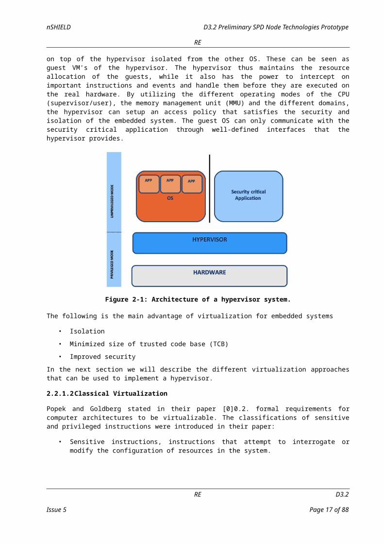
The figure below describes the hypervisor architecture. We have the hypervisor running in the most privileged mode right above the hardware. The guest OS together with its applications are in turn running on top of the hypervisor in a less privileged mode. There is also a security critical application running on top of the hypervisor isolated from the other OS. These can be seen as guest VM's of the hypervisor. The hypervisor thus maintains the resource allocation of the guests, while it also has the power to intercept on important instructions and events and handle them before they are executed on the real hardware. By utilizing the different operating modes of the CPU (supervisor/user), the memory management unit (MMU) and the different domains, the hypervisor can setup an access policy that satisfies the security and isolation of the embedded system. The guest OS can only communicate with the security critical application through well-defined interfaces that the hypervisor provides.
Figure 2-1: Architecture of a hypervisor system.
The following is the main advantage of virtualization for embedded systems
RE D3.2
Issue 5 Page 13 of 70

D3.2 Preliminary SPD Node Technologies Prototype nSHIELD
RE
• Isolation
• Minimized size of trusted code base (TCB)
• Improved security
In the next section we will describe the different virtualization approaches that can be used to implement a hypervisor.
2.2.1.2 Classical Virtualization
Popek and Goldberg stated in their paper [0]0.2 formal requirements for computer architectures to be virtualizable. The classifications of sensitive and privileged instructions were introduced in their paper:
• Sensitive instructions, instructions that attempt to interrogate or modify the configuration of resources in the system.
• Privileged instructions, instructions that trap if executed in an unprivileged mode, but execute without trapping when run in a privileged mode.
To be able to fully virtualize architecture, Popek and Goldberg stated that the sensitive processor instructions had to be equal to the set of privileged instructions or a subset of it. This criterion has now been termed classically virtualizable. In the following section we present different types of virtualization techniques as each has its own advantages and disadvantages.
2.2.1.3 Full Virtualization
As discussed earlier, because the hypervisor resides in the privileged mode, the guest OS which is residing in the less privileged mode, cannot execute its privileged instructions. Instead the execution of these privileged instructions has to be delegated to the hypervisor. One way to do this is through applying full virtualization. The idea behind it is, whenever software is trying to execute privileged instructions in an unprivileged mode, it will generate a trap into the privileged mode. Because the hypervisor resides in the privileged mode, one could write a trap handler that emulates the privileged instruction that the guest OS is trying to execute. This way, through trap-and-emulate, all the privileged instructions that the guest OS is trying to execute will be handled by the hypervisor, while all other non-privileged instructions can be run directly on the processor. The advantage with full virtualization is that the virtualized interfaces provided to the guest operating system has identical interfaces compared to the real machine. This means that the system can execute binary code without any changes, neither the operating systems nor their applications need any adaptation to the virtual machine environment and all code that had originally been written to the physical machine can be reused.
However to apply full virtualization it requires that all sensitive instructions are a subset of the privileged instructions, in order for it to trap to the hypervisor. This is why Popek and Goldberg's criteria classically virtualizable have to be fulfilled in order to apply full virtualization and most general purpose CPU's does not support this. A downside with full virtualization is, since a trap is generated for every privileged instruction, it adds significant overhead as each privileged instruction is emulated with many more instructions. In turn we get excellent compatibility and portability.
2.2.1.4 Binary Translation
In the 90s, the x86 architecture was prevalent in desktop and server computers but still, full virtualization could not be applied to the architecture. Because the x86 architecture contains sensitive instructions that are not a subset of the privileged instructions [0]0.3, it fails to fulfil Popek and Goldberg's criteria ''classically virtualizable``. These sensitive instructions would not trap to the hypervisor and it was not possible to execute these sensitive instructions in the unprivileged mode, making full virtualization not possible. VMware has however shown that, with binary translation one could also achieve the same benefits as full virtualization on the x86 architecture. Binary translation solves this problem by scanning the guest code at load or runtime for all sensitive instructions that do not trap before they are executed, and replaces them with appropriate calls to the hypervisor. The technique used is quite complex and increases the code size running in the highest privileged mode, increasing the TCB. Through a security
D3.2 RE
Page 14 of 70 Issue 5
nSHIELD D3.2 Preliminary SPD Node Technologies Prototype
RE
point of view, one would want the amount of code in the privileged mode to be as small as possible in order to minimize the area of the attack surface. This could affect the security and isolation properties of the entire system.
Because of the complex scanning techniques of binary translation, the performance overhead is larger than full virtualization. However, binary translation has provided the benefits of full virtualization on an architecture that was previously not fully virtualizable.
2.2.1.5 Paravirtualization
Para-virtualization was designed to keep the protection and isolation found in the full virtualization but without the performance overheads and implementation complexity in the hypervisor. However, in order to achieve this, you have to sacrifice the convenience of running an operative system unmodified on the hypervisor.
In a paravirtualized system, all the privileged instructions in the operating system kernel have to be modified to issue the appropriate system call that communicates directly with the hypervisor, also called hypercalls. This makes paravirtualization able to achieve better performance compared to full virtualization due to the direct use of appropriate hypercalls instead of multiple traps and instruction decoding. Examples on hypercall interfaces provided by the hypervisor are critical kernel operations such as memory management, interrupt handling, kernel ticks and context switching. As each hypercall offers a higher level of abstraction compared to emulation at the machine instruction level, the amount of work that a hypercall can do is a lot more efficient compared to emulating each sensitive machine instruction.
Most ARM architectures1, which are very common in embedded systems, however do not fulfil the criteria of "classically virtualizable". This means that virtualization on the ARM architecture can either be achieved through binary translation or paravirtualization. Because embedded systems generally are resource constrained, the performance overhead that binary translation generates is too high, making paravirtualization the best approach for the ARM architecture.
However, the drawback with paravirtualization is that each operating system has to be adapted to the new interface of the hypervisor. This can be quite a large task, and closed-source operating systems like Windows cannot be modified by anyone other than the original vendor. Still, in embedded systems it is common for the developers to have full access to the operating system's source code. The disadvantage to run a modified operating system is not always a big issue; the operating system needs to be ported to the custom hardware either way and at the same time, it performs better.
2.2.1.6 Hardware Virtualized Extensions ARM
Focusing on the ARM architecture, it is worth to mention that it offers a hardware security extension called TrustZone [0]0.4 in ARMv6 or later architectures. It offers support for switching between two separate states, called worlds. One world is secure which is intended to run trusted software, while the other world is normal, where the untrusted software runs.
A single core is able to execute code from both worlds, and at the same time ensuring that the secure world software is protected from the normal world. Thus, the secure world controls all partitioning of devices, interrupts and coprocessor access. To control the switch between the secure and normal world, a new processor mode has been introduced called Monitor mode, preventing data from leaking from the secure world to the normal world.
In the latest ARMv7 architecture, the Cortex-A15 processor further introduced hardware virtualization extensions that allow the architecture to be classically virtualized by bringing a new mode called hyp as the highest privileged mode, hardware support for handling virtualized interrupts, and extra functionality to support and simplify virtualization. These extra extensions add features to make full virtualization possible and improve the speed of virtualization [0]0.5.
1 With the exception of the new ARMv7 Cortex-A15
RE D3.2
Issue 5 Page 15 of 70

D3.2 Preliminary SPD Node Technologies Prototype nSHIELD
RE
2.2.1.7 Virtualization in Embedded Systems
As the nSHIELD project focuses in embedded systems, we will look into the functionality of virtualization that is inherited from their previous use in servers and workstations. The properties between the two systems are however completely different. For server and desktop computers, power, space or weight is of no concern, while for embedded systems the contrary often holds true. So a re-evaluation in the light of embedded systems is necessary.
Because the server and desktop markets are largely dominated by the x86 architecture, virtualization approaches have been specifically tailored for this architecture. Also for server and desktops, usually the number one requirement is to be able to run all commodity operating systems without modifications. This was the advantage that full virtualization had over paravirtualization, but in embedded systems, it is common for the developer to have access to the full source code of the operating system. Usually the developers have to port the operating system to the specialized embedded hardware, thus using paravirtualization is not such big disadvantage anymore.
2.2.1.8 Isolation
In servers and desktops, all virtualization approaches featured strong isolation between the VM's and is usually all that is needed to provide a secure and robust environment. A VM that is affected by malicious software will be confined to that VM, as the isolation prevents it from spreading to other VM's. For server and desktop use, this is usually all that is needed because there is no need for VM's to interact with each other in any other ways from how real computers communicate, that is through the network. However in embedded systems, multiple systems generally contribute to the overall function of the device. Thus the hypervisor needs to provide a secure communication interface between the isolated VM's, much like a microkernel IPC, while still preserving the isolation of the system [0]0.6.
2.2.1.9 Trusted Computing Base
In embedded systems, the size of the memory has a big effect on the cost of the device. They are generally designed to provide their functionality with minimal resources, thus cost and power sensitive devices benefits from a small code size.
In other devices where the highest levels of safety or security are required, every code line represents an additional potential threat and cost. This is called the trusted code base and includes all software that is run in privileged mode, which in general cases include the kernel and any software modules that the kernel relies on. In security critical applications, all trusted code may have to go through extensive testing. In some cases where security needs to be guaranteed, the security of the system has to be proven mathematically correct and undergo a formal verification. This makes it crucial that the size of the trusted code base is as small as possible as it will make formal verification easier.
In virtualization, the trusted code base will include the hypervisor as it now runs in the most privileged mode. For data server hypervisors like Xen [0]0.7, its code base is about 100,000 lines of code which is quite large, but the biggest problem is that is also relies on a full Linux system in the privileged mode. This makes the trusted code base several millions lines of code which makes a formal verification impossible. The reason the Xen and similar hypervisors is so large, is because it is mainly designed for server stations. Most policies are implemented inside the privileged code, which embedded systems have very little, or no use of.
In a microkernel the servers provide all the policies, while the microkernel only provides the mechanism to execute these policies. It aims to reduce the amount of privileged code to a minimum but still provide the basic mechanism to run an operating system on it. This result in a small trusted code base and from a security perspective, for example the L4 microkernel has a big advantage as the size is only about 10,000 lines of code and has also undergone formal verification [0]0.8.
2.2.1.10 Performance
Most often performance is much more crucial and expensive for embedded systems. To be able to get the most out of the hardware, a hypervisor for embedded systems must perform with a very low overhead as
D3.2 RE
Page 16 of 70 Issue 5
nSHIELD D3.2 Preliminary SPD Node Technologies Prototype
RE
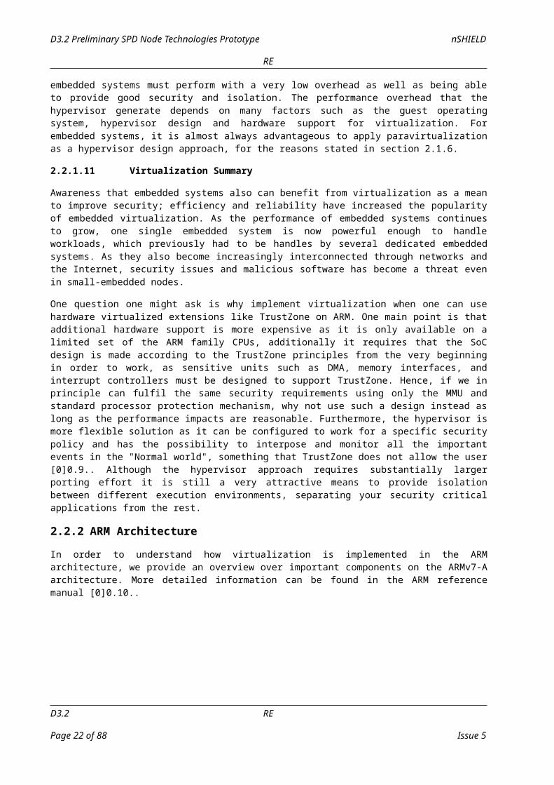
well as being able to provide good security and isolation. The performance overhead that the hypervisor generate depends on many factors such as the guest operating system, hypervisor design and hardware support for virtualization. For embedded systems, it is almost always advantageous to apply paravirtualization as a hypervisor design approach, for the reasons stated in section 2.1.6.
2.2.1.11 Virtualization Summary
Awareness that embedded systems also can benefit from virtualization as a mean to improve security; efficiency and reliability have increased the popularity of embedded virtualization. As the performance of embedded systems continues to grow, one single embedded system is now powerful enough to handle workloads, which previously had to be handles by several dedicated embedded systems. As they also become increasingly interconnected through networks and the Internet, security issues and malicious software has become a threat even in small-embedded nodes.
One question one might ask is why implement virtualization when one can use hardware virtualized extensions like TrustZone on ARM. One main point is that additional hardware support is more expensive as it is only available on a limited set of the ARM family CPUs, additionally it requires that the SoC design is made according to the TrustZone principles from the very beginning in order to work, as sensitive units such as DMA, memory interfaces, and interrupt controllers must be designed to support TrustZone. Hence, if we in principle can fulfil the same security requirements using only the MMU and standard processor protection mechanism, why not use such a design instead as long as the performance impacts are reasonable. Furthermore, the hypervisor is more flexible solution as it can be configured to work for a specific security policy and has the possibility to interpose and monitor all the important events in the "Normal world", something that TrustZone does not allow the user [0]0.9. Although the hypervisor approach requires substantially larger porting effort it is still a very attractive means to provide isolation between different execution environments, separating your security critical applications from the rest.
2.2.2 ARM Architecture
In order to understand how virtualization is implemented in the ARM architecture, we provide an overview over important components on the ARMv7-A architecture. More detailed information can be found in the ARM reference manual [0]0.10.
2.2.2.1 Introduction
The ARM core is RISC architecture. RISC philosophy concentrates on reducing the complexity of instructions performed by the hardware, while putting a greater demand on the compiler. This way, each instruction is of fixed length of 32-bits and can be completed in a single clock cycle, while also allowing the pipeline to fetch future instruction before decoding the current instruction.
In contrast to RISC, CISC architectures relies more on hardware for instruction functionality, which consequently makes the instructions more complex. The instructions are often variable in size and take many cycles to execute.
As a pure RISC processor is designed for high performance, the ARM architecture uses a modified RISC design philosophy that also targets code density and low power consumption. As a result, the processor has become dominant in mobile embedded systems. It was reported that in 2005, about 98% of more than a billion mobile phones sold each year used at least one ARM processor and as of 2009, ARM processors accounted for approximately 90% of all embedded 32-bit RISC processors [0]0.11.
2.2.2.2 Current Program Status Register
Beside the 16 general-purpose registers from r0 to r15 in the ARM architecture, we have the CPSR, which the ARM processor uses to monitor, and control internal operations. The CPSR is used to configure the following:
• Processor mode: Can be in seven different processor modes, discussed in the next section.
RE D3.2
Issue 5 Page 17 of 70

D3.2 Preliminary SPD Node Technologies Prototype nSHIELD
RE
• Processor state: The processor state determines if ARM, Thumb or the Jazelle instruction set is being used2.
• Interrupt masks: Interrupt masks are used to enable or disable the FIQ and IRQ interrupts.
• Condition flags: Contains the results of ALU operations, which update the CPSR condition flags. These are instructions that specify the S3 instruction suffix and are used for conditional execution to speed up performance.
2.2.2.3 Processor mode
The ARM architecture contains seven processor modes, which are either privileged or unprivileged. It contains one unprivileged mode User and the following modes are all privileged.
• Supervisor
• Fast interrupt request (FIQ)
• Interrupt request (IRQ)
• Abort
• Undefined
• System
When power is applied to the processor, it starts in Supervisor mode and is generally also the mode that the operating system operates in. FIQ and IRQ correspond to the two interrupt levels available on the ARM architecture. When there is a failed attempt to access memory, the processor switches to abort mode. System mode is generally used for other privileged OS kernel operations. Undefined mode is used when the processor encounters an instruction that is undefined or unsupported by the implementation. Lastly, the unprivileged mode User mode is generally used for programs and applications run on the operating system. In order to have full read/write access to the CPSR, the processor has to be in privileged mode.
2.2.2.4 Interrupts and Exceptions
Whenever an exception or interrupt occurs, the processor suspends the ongoing execution and jumps into the corresponding exception handler in the vector table. The vector table is located in a specific memory address and each 4-byte entry in the table contains an address, which points to the start of a specific routine:
• Reset: Location of the first instruction executed by the processor at power up. The reset vector branches to the initialization code.
• Undefined: When the processor cannot decode an instruction, it branches to the undefined vector. Also occurs when a privileged instruction is executed from the unprivileged user mode.
• Software interrupt: Occurs when the SWI instruction is used. The instruction is frequently used by applications when invoking an operating system routine. When used, the processor will switch from user mode to supervisor mode.
• Prefetch abort: Occurs when the processor trying to fetch an instruction from an address without the correct access permissions.
• Data abort: Occurs when the processor attempts to access data memory without correct access permissions.
• Interrupt request: Used by external hardware to interrupt the normal execution flow of the processor.
2 ARM - 32 bit, Thumb - 16-bit, Jazelle - 8 bit (Java byte code support)
3 Certain instructions have the possibility to add an optional S suffix to the instruction
D3.2 RE
Page 18 of 70 Issue 5

nSHIELD D3.2 Preliminary SPD Node Technologies Prototype
RE
What the specific routine will do is generally controlled by the operative system. However, when applying virtualization to the system, all the routines will be implemented inside the hypervisor.
2.2.2.5 Coprocessor
The ARM architecture makes it possible to extend the instruction set by adding up to 16 coprocessors to the processor core. This makes it possible to add more support for the processor, such as floating-point operations.
Coprocessor 15 is however reserved for control functions such as the cache, memory management unit (MMU) and the translation looks aside buffer (TLB). In order to understand how the hypervisor can provide improved security by isolating different resources, it is important to understand the mechanics behind the memory management of the ARM architecture.
2.2.2.6 Memory Management Unit
Through coprocessor 15 on the ARM architecture, the MMU can be enabled. Without an MMU, when the CPU accesses memory, the actual memory addresses never change and map one-to-one to the same physical address. However with an MMU, programs and data are run in virtual memory, an additional memory space that is independent of the physical memory. This means that the virtual memory addresses have to go through a translation step prior each memory access. It would be quite inefficient to individually map the virtual to physical translation for every single byte in memory, so instead the MMU divides the memory into contiguous sections called pages. The mappings of the virtual addresses to physical addresses are then stored in the page table. In addition to this, access permission to the page table is also configurable.
To make the translation more efficient, a dedicated hardware, the TLB handles the translation between virtual and physical addresses and contains a cache of recently accessed mappings. When a translation is needed, the TLB is searched first, and if not found, a page walk occurs which means it continues to search through the page table. When found, it will be inserted into the TLB, possibly evicting an old entry if the cache is full.
The virtualization of memory efficiently supports multitasking environments as the translation process allows the same virtual address to be held in different locations in the physical memory. By activating different page tables during a context switch, it is possible to run multiple tasks that have overlapping virtual addresses. This approach allows all tasks to remain in physical memory and still be available immediately when a context switch occurs.
2.2.2.7 Page Tables
The page table descriptors are architecture specific, and we will show how the ARMv7-A architecture looks like.
There are two levels of page tables in the ARM MMU hardware. The master page table contains 4096 page table entries known as first level descriptors, each describing 1MB of virtual memory, enabling up to 4GB of virtual memory. The level one master page table can either be a super section descriptor, section descriptor or page table descriptor.
• Supersection descriptor: Consists of 16MB block of memory. Because each first level page table entry covers a 1MB region of virtual memory, the 16MB supersections require that 16 identical copies of the first level descriptor of the supersection exist in the first level page table.
• Section descriptor: Consists of 1MB block of memory
• Page descriptor: Provides the base address to a second level descriptor that specifies how the associated 1MB is mapped. It's either a large or small page descriptor.
Second level descriptors:
• Large page descriptor: Consist of 64KB blocks of memory
RE D3.2
Issue 5 Page 19 of 70

D3.2 Preliminary SPD Node Technologies Prototype nSHIELD
RE
• Small page descriptor: Consist of 4KB blocks of memory
The large page descriptor thus has 64 entries while a small page has 256 entries, splitting the 1MB that the table describes into 64KB and 4KB of blocks respectively. The figure below shows the overview of the first and second level page tables.
Figure 2-2: Page table fetch.
The translation process always begins in the same way at system start-up; the TLB does not contain a translation for the requested virtual address so it initiates a level one fetch. If the address is a supersection or section-mapped access it returns the physical address and the translation is finished. But if it is a page-mapped access, it requires an additional level two fetch into either a large or small page in where the TLB can extract the physical address.
Common for all levels of page tables is that it contains configuration for cache, buffer and access permission. The domain configuration is however only configurable for the first level descriptors, associating the page table with one of the 16 MMU domains. This means that it can only be applied at 1MB granularity; individual pages cannot be assigned to specific domains.
2.2.2.8 Domain and Memory Access Permissions
Memory accesses are primarily controlled through the use of domains, and a secondary control is the access permission set in the page tables. As mentioned before, the first level descriptors could be assigned to one of the 16 domains. When a domain has been assigned to a particular address section, it must obey the domain access rights assigned to that domain. Domain access permissions can be configured through the CP15:c3 register and each of the 16 available domains can have the following bit configurations.
• Manager (11): Access to this domain is always allowed
• Client (01): Access controlled by permission values set in the page table entry
• No Access (00): Access to this domain is always denied
If the configuration is set to Client, it will look at the access permission of the corresponding page table. The table below shows how the MMU interprets the two bits in the AP bit field of the page table.
Table 2-1: Page table AP Configuration
D3.2 RE
Page 20 of 70 Issue 5

nSHIELD D3.2 Preliminary SPD Node Technologies Prototype
RE
AP bit User mode Privileged mode
00 No access No access
01 No access Read and write
10 Read only Read and write
11 Read and write Read and write
With the help of the domain access control and page-level protection, we can isolate different memory regions in the system to achieve the wanted security configuration.
2.2.2.9 Summary
This concludes the ARM architecture background information where we described the fundamental mechanisms necessary to apply virtualization to a system. In the next section, we will go into the detailed design on how the SICS hypervisor is designed and implemented.
2.2.3 SICS Hypervisor
The hypervisor software was designed for the ARM architecture, with the main goal to improve the security of an embedded system through the isolation properties that it can provide. This is achieved by only letting the hypervisor execute in privileged mode, where it can control all the systems hardware resources and control the access policy and security of the running application and operating systems. In our case, the SICS hypervisor uses paravirtualization to virtualize the guest system to run on top of the hypervisor in a lower privilege mode (user mode).
By having several virtual guest modes, each with its own execution context and memory access configuration, the hypervisor can enforce the memory isolation between the operating system, its applications and most importantly, the security critical applications.
2.2.3.1 Guest Modes
The hypervisor supports arbitrary number of "virtual" guest modes. As guest modes have their own memory configuration and execution context, the hypervisor always controls which current guest mode is executing. There are currently four virtual guest modes defined in the hypervisor:
• Kernel mode: Execution context for guest kernel
• Task: Execution context for user applications
• Trusted: Execution context for security critical applications
• Interrupted mode: Execution context for interrupts
These virtual guest modes are necessary in the ARM architecture, because we only have two security rings, privileged and unprivileged. The hypervisor has to reside in the privileged ring while all other software such as, the operating system, task applications and security critical application have to reside in the unprivileged ring. Therefore to keep the separation between the software located in the unprivileged ring, we need these virtual guest modes.
Depending on which the current guest mode is, the memory access to the different domains can be set up differently to suit the security needs of the system. The hypervisor then makes sure that the correct corresponding virtual guest mode is running, depending on whether kernel, task or trusted code is executing. Whenever an interrupt is generated, the hypervisor will change the guest mode to interrupt mode. In the next section we will go through how memory isolation is achieved.
RE D3.2
Issue 5 Page 21 of 70
D3.2 Preliminary SPD Node Technologies Prototype nSHIELD
RE
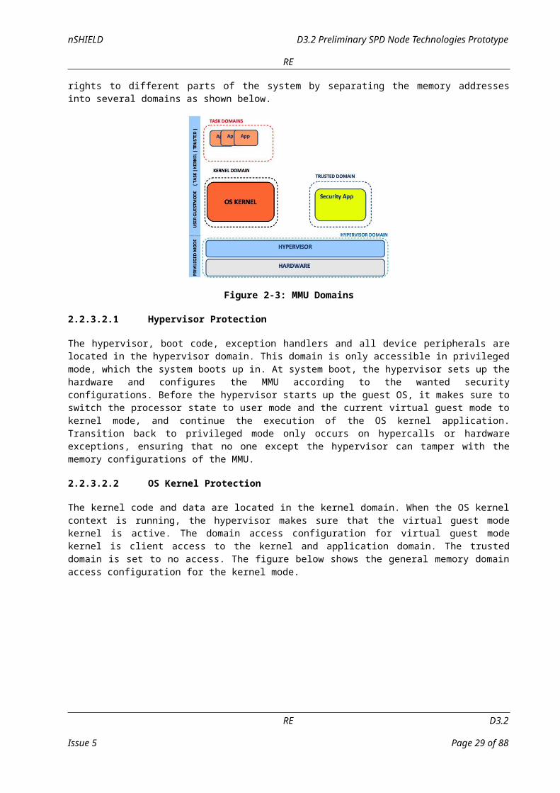
2.2.3.2 Memory Protection
With the help of the linker script file, we can decide where the hypervisor, kernel, task and trusted code are placed in the memory. Through the domain access permission and the page table access permission we can setup access rights to different parts of the system by separating the memory addresses into several domains as shown below.
Figure 2-3: MMU Domains
2.2.3.2.1 Hypervisor Protection
The hypervisor, boot code, exception handlers and all device peripherals are located in the hypervisor domain. This domain is only accessible in privileged mode, which the system boots up in. At system boot, the hypervisor sets up the hardware and configures the MMU according to the wanted security configurations. Before the hypervisor starts up the guest OS, it makes sure to switch the processor state to user mode and the current virtual guest mode to kernel mode, and continue the execution of the OS kernel application. Transition back to privileged mode only occurs on hypercalls or hardware exceptions, ensuring that no one except the hypervisor can tamper with the memory configurations of the MMU.
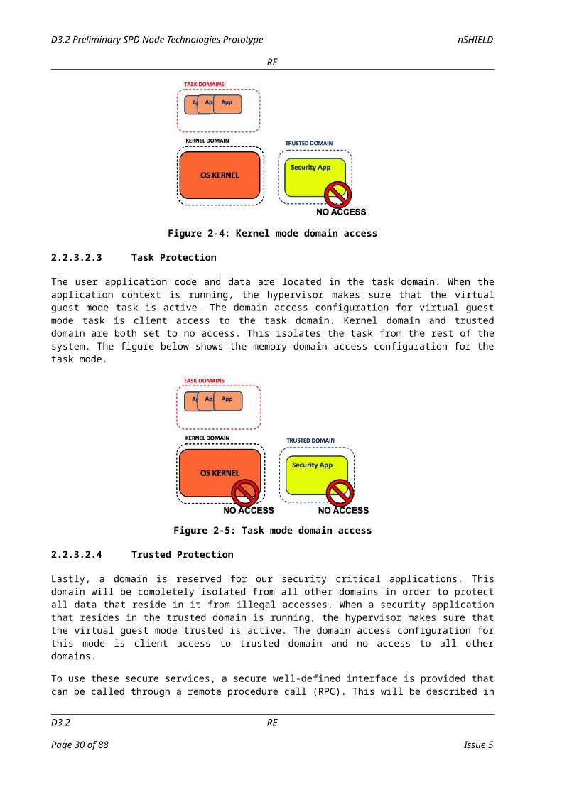
2.2.3.2.2 OS Kernel Protection
The kernel code and data are located in the kernel domain. When the OS kernel context is running, the hypervisor makes sure that the virtual guest mode kernel is active. The domain access configuration for virtual guest mode kernel is client access to the kernel and application domain. The trusted domain is set to no access. The figure below shows the general memory domain access configuration for the kernel mode.
Figure 2-4: Kernel mode domain access
D3.2 RE
Page 22 of 70 Issue 5
nSHIELD D3.2 Preliminary SPD Node Technologies Prototype
RE
2.2.3.2.3 Task Protection
The user application code and data are located in the task domain. When the application context is running, the hypervisor makes sure that the virtual guest mode task is active. The domain access configuration for virtual guest mode task is client access to the task domain. Kernel domain and trusted domain are both set to no access. This isolates the task from the rest of the system. The figure below shows the memory domain access configuration for the task mode.
Figure 2-5: Task mode domain access
2.2.3.2.4 Trusted Protection
Lastly, a domain is reserved for our security critical applications. This domain will be completely isolated from all other domains in order to protect all data that reside in it from illegal accesses. When a security application that resides in the trusted domain is running, the hypervisor makes sure that the virtual guest mode trusted is active. The domain access configuration for this mode is client access to trusted domain and no access to all other domains.
To use these secure services, a secure well-defined interface is provided that can be called through a remote procedure call (RPC). This will be described in the next section. A typical scenario is a commodity operating system and an isolated trusted domain offering secure services to untrusted applications.
The figure below shows the memory access configuration for the trusted mode.
Figure 2-6: Trusted mode domain access
2.2.3.3 Hypervisor Configuration
For each system running on the hypervisor, there is a configurable file that contains the setup of the running system. It contains information regarding which address space and domain each region reside in
RE D3.2
Issue 5 Page 23 of 70

D3.2 Preliminary SPD Node Technologies Prototype nSHIELD
RE
and capability list of each virtual guest mode, what it is allowed to do and not. This configuration file is parsed by the hypervisor at start-up to setup the hypervisor system. There is one configuration file for each platform and OS port.
2.2.3.4 Hypercall Interface
To provide a safe access to privileged functionality, the hypervisor has a hypercall interface available for the guest OS to use. Because the OS kernel now runs in unprivileged mode, all the previous privileged instructions that the kernel could do itself, now has to be delegated to the hypervisor through hypercalls. These are invoked through the SWI instruction. A list of the offered hypercalls can be seen in the table below. Each hypercall is verified by the hypervisor to confirm that it is an allowed operation. Important checks consists of where the call origin from, which virtual guest mode, address space and memory access configurations.
Table 2-2: Hypercall interface
Hypercall Description
BOOT_INFO Provides the hypervisor with OS specific information to setup the system
SET_CPU_CR Sets the CPU control register
GET_CPU_CR Gets the CPU control register
IRQ_SAVE Saves the state of the IRQ
IRQ_RESTORE Restores the state of the IRQ
INTERRUPT_SET Sets the state of the IRQ and FIQ in the CPSR
END_INTERRUPT Gives back execution to the interrupted context (called after hardware interrupts)
IRQ_DISABLE Disables IRQ
IRQ_ENABLE Enables IRQ
FLUSH_ALL Flushes all caches
TLB_INVALIDATE Invalidates translation look aside buffer
CACHE_INVALIDATE Caches invalidate operations on virtual address
SET_PAGE Page table operations
CREATE_SECTION Creates a section page table and inserts it in the master page table
RESTORE_USER_REGS Used to switch execution context
SWITCH_MM Sets another page table for user process
RPCUsed to communicate between different guest modes. (Used to change virtual guest mode and execute security critical applications).
END_RPC Gives back execution to the RPC caller
D3.2 RE
Page 24 of 70 Issue 5

nSHIELD D3.2 Preliminary SPD Node Technologies Prototype
RE
2.2.3.5 Hardware Exceptions
Whenever a hardware exception or an interrupt occurs, the processor suspends the ongoing execution context, switches to privileged mode and jumps into the corresponding exception handler. These have all been redirected to the respective hypervisor handler routine.
• Undefined: When the hypervisor encounters an undefined exception, it means that the guest OS tried to execute an instruction that the ARM processor could not understand. The hypervisor can either decide to halt the execution or jump over it and continue execution.
• Software interrupt: This is the hypercall handler. When the guest OS executes a software interrupt, the handler decodes the requested hypercall and executes the requested operation. This can also be a user application requesting the OS kernel to perform a system call, in which case the hypervisor redirects execution to the OS kernel.
• Prefetch abort: When the guest OS attempts to fetch an instruction from an address without correct access permissions, the hypervisor first check the memory address if its an legal access and redirects the execution to the OS kernel own prefetch abort handler (if available). If it’s an illegal access, the hypervisor can halt execution or jump over it.
• Data abort: When the guest OS attempts to access data memory without correct access permissions, the hypervisor check the memory address if it’s an legal access and redirects it to the OS kernels own data abort handler. If it’s an illegal access, the hypervisor can halt execution or jump over it.
• Interrupt: Hypervisor interrupt handler saves execution context of the interrupted task, which includes the CPU registers, state and guest mode. It then disables interrupts for the guest OS and redirects to the OS kernels interrupt handler. When the guest OS has finished handling the interrupt, it gives back execution to the hypervisor which restores the execution context of the last interrupted task.
Whenever the hypervisor gets execution, it saves the interrupted virtual guest mode and its execution context in order to know where to resume execution when it is finished with its operations.
2.2.3.6 Hypervisor Development Progress
The hypervisor was first developed for the ARMv5 architecture, specifically the ARM926EJ-S CPU supporting the FreeRTOS kernel as a paravirtualized guest. All hardware and peripherals were initially simulated with the simulation software Open Virtual Platforms (OVP) [0]0.12. A generic OVP barebone platform was used.
As the first hypervisor prototype was deemed successful in terms that security was significantly increased because of the added isolation properties, efforts were made to add more platform support, hypervisor functionality and use real hardware. The following are the progress list of the hypervisor.
• Functional hypervisor on ARMv5 926EJ-S CPU with paravirtualized freeRTOS port running on simulation software (OVP)
• Added security critical application running isolated from the rest of the system on top of the hypervisor to test real use case.
• Added hypervisor DMA virtualization to prevent illegal hardware access.
• Added support for ARMv7 Cortex A8 on hypervisor (OVP)
• Modified hypervisor to be more platform and architecture independent through a hardware abstraction layer (HAL). Increased portability.
• Added real hardware support for the hypervisor (BeagleBoard and BeagleBone). Working in real hardware.
• Paravirtualizing Linux kernel and adding hypervisor functionality to support Linux (Current)
RE D3.2
Issue 5 Page 25 of 70

D3.2 Preliminary SPD Node Technologies Prototype nSHIELD
RE
2.2.4 FreeRTOS Port
FreeRTOS is a free open source real time operating system that we have ported to work on the SICS hypervisor. It is very simple and small, consisting of approximately 4000 lines of code, with no file systems, complex memory management or device drivers.
Thus paravirtualizing FreeRTOS is a relatively simple task, compared to for example the Linux kernel. We will show the main modifications required for it to work on the hypervisor. The figure below shows the basic structure of the FreeRTOS system.
Figure 2-7: FreeRTOS hypervisor system
2.2.4.1 FreeRTOS Kernel
The core FreeRTOS kernel has remained almost completely unchanged except from some minor modifications on how the task applications are allocated. Previously, the kernel allocated memory for all tasks from the same heap. We added extra functionality to allocate task memory from a pool of separated heaps which also gives you the possibility to create isolation between the different application tasks. Except from this change, the core kernel has stayed unmodified.
2.2.4.2 Platform Dependent Code
The platform dependent code is responsible for carrying out critical low-level operations, which requires privileged instructions. These have been paravirtualized replacing all the privileged instructions with hypercalls.
2.2.4.3 Memory Management
Originally, FreeRTOS does not have any memory protection, as it does not use the MMU to setup the system. All memory accesses use physical addresses and are unprotected. This means that security is non-existent for the system as user applications have full access to all hardware resources and the kernel. Because there were no memory management for the FreeRTOS we had full freedom to decide the location of all software regions, access control and how the memory addresses will be mapped.
What we have done is through the linker script, defined distinct addresses for the different software regions (kernel address space and user task address space), and through the MMU, domain and page table settings, setup a configuration that effectively enforces an access policy that provides us with memory isolation between our hypervisor, OS kernel and user applications. This is used in our first prototype for the nSHIELD 3.3 deliverable and more details on the configuration can be seen in D3.3.
D3.2 RE
Page 26 of 70 Issue 5

nSHIELD D3.2 Preliminary SPD Node Technologies Prototype
RE
2.2.4.4 Hypercalls / System Calls
As the FreeRTOS originally did not have any kernel and user space separation, user applications could directly use the kernel API to call kernel functions. This is generally not the case in more complex operating systems where applications have to use system calls through the SWI instruction to perform kernel operations.
With the hypervisor in place creating separation between kernel and user address space, it can no longer access the kernel API. To solve this, the kernel API functions have been wrapped around RPC hypercalls that changes the virtual guest mode, this in order to get access to the kernel address space. This provides a secure interface to use the kernel API without compromising the security of the kernel. When the kernel API call is finished, an end RPC hypercall is issued to change the current guest mode back to task mode, disabling the kernel domain and yielding back to the calling task.
2.2.4.5 Interrupt Handling
The FreeRTOS scheduler relies on the hardware timer to schedule tasks. In order for FreeRTOS to work as usual, the Hypervisor redirects all timer interrupts to the FreeRTOS timer tick handler, which schedules the next task.
When FreeRTOS is scheduling a new task, it saves the current tasks execution context in its data structures and uses a hypercall to load the next running task context.
2.2.4.6 Summary
In our experience, paravirtualizing the very small OS FreeRTOS was relatively easy to accomplish. We went from a system with non-existent security to a hypervisor protected secure environment.
2.2.5 Linux Port
Work is currently in progress of porting the Linux kernel version 2.6.34.3 to our hypervisor using paravirtualization. The main reason behind choosing this specific kernel release is that the simulation software OVP already has a working Linux kernel running on an ARM Cortex A8 Integrator CP platform. To simplify things, the Linux kernel 2.6.34.3 has been modified and compiled with only UART support as a start. The kernel starts the bash shell command that communicates with a serial console through the UART. This will be the start base of our porting efforts. We will issue the biggest challenges with the port.
• Memory management
• Interrupt service routines
• Processes
• Hypercalls & System Calls
• Platform support
2.2.5.1 Memory Management
One requirement for Linux to work is that it requires a one to one mapping of the physical memory to the kernels virtual address space. This is given to the Linux kernel by the hypervisor during the boot/initialization phase. The hypervisor provides the page table structure for the OS and keep track of which physical memory addresses that belong to the OS. Any attempts to access memory outside of the OS will generate an access fault. Currently, the configuration is static in the first iteration of the port and more advanced features can be added when we have a more stable version. As the current goal is to successfully run a single guest, we don’t need any advanced OS like memory management in the hypervisor.
As the Linux kernel no longer has permission to communicate with the MMU, it has to go through the hypervisor to update these parts of the CPU. The hypervisor will also be responsible for updating the
RE D3.2
Issue 5 Page 27 of 70

D3.2 Preliminary SPD Node Technologies Prototype nSHIELD
RE
Linux page table whenever it needs more memory, or when there is free memory that it no longer needs. Another instance is when a certain application wants access to something in memory that is not yet mapped to physical memory; it will generate a page fault. The hypervisor need to let the Linux kernel know that it must look up the physical address to map it into the specific application. As the true hardware page tables are kept inside the hypervisor the OS have a shadow page table to be able to keep track of the page attributes in order to properly map and unmap pages for the user processes.
Modifications to the memory management of the Linux kernel also includes giving the SICS hypervisor responsibility for all CPU operations such as flushing/invalidating the TLB and cache.
2.2.5.1.1 Page Tables in ARM Linux
Hardware wise, ARM has a two level page table structure, where the first level has 4096 entries, and the second level has 256 entries4. Each entry is one 32-bit word. The problem here is that the page tables do not contain any "accessed” or “dirty” bits which specify if the address have been accessed or written. The Linux kernel uses this information for its memory management operations such as resolving page faults, freeing memory and swapping memory. Thus, Linux has to keep its own copy of the page tables that contains the missing information. Another detail is that Linux has a three level page table structure 5 which in the ARM port is wrapped to fit in a two level page table structure using only the page global directory (PGD) and page table entry (PTE).
Linux therefore is tweaked to having 2048 entries in the first level, each of which is 8 bytes (i.e. two hardware pointers to the second level). The second level contains two hardware PTE tables (of 256 entries each) arranged contiguously, followed by Linux version which contain the state information that Linux needs. Therefore, the PTE level ends up with 512 entries [0]0.13.
2.2.5.1.2 Linux Kernel Mappings
The Linux kernel has a very specific virtual memory layout that we have to follow, in order to not break kernel functionality. Mappings, which collide with the above areas, may result in a non-bootable kernel, or may cause the kernel to eventually panic at run time.
Looking at the table below [0]0.14, we can see that the virtual address space of a user process in native Linux kernel range from 0x1000 to PAGE_OFFSET6 – 1. This address space can be accessed in either user or privileged mode. The address space from PAGE_OFFSET to 0xFFFF FFFF belongs to the kernel and can only be accessed in privileged mode. The hypervisor virtual guest modes will mimic these privilege states in order to enforce these rules.
The hypervisor software also needs a mapping and can be put between VMALLOC_END - 0xFEFFFFFF, which is free for platform use. We have decided that a suitable location is 1MB from 0xF000 0000 is mapped for the hypervisor.
Table 2-3: Kernel Memory Layout on ARM Linux
Start End Use
0xFFFF 8000 0xFFFF FFFF Copy_user_page / Clear_user_page use
0xFFFF 4000 0xFFFF FFFF Cache aliasing on ARMv6 and later CPUS
0xFFFF 1000 0xFFFF 7FFF Reserved. Platforms must not use this address range
4 Linux ARM kernel only uses small pages of 4KB for second level descriptors
5 This comes from the x86 architecture
6 Normally set to 0xC000 0000 which gives a user/kernel split of 3GB/1GB
D3.2 RE
Page 28 of 70 Issue 5
nSHIELD D3.2 Preliminary SPD Node Technologies Prototype
RE
0xFFFF 0000 0xFFFF 0FFFCPU vector page. The CPU vectors are mapped here if the CPU supports vector relocation (control register V bit)
0xFFFE 0000 0xFFFF 0FFFXScale cache flushes area. This is used in proc-xscale.S to flush the whole data cache. (XScale does not have TCM.)
0xFFFE 8000 0xFFFE FFFF DTCM mapping area for platforms with DTCM mounted inside the CPU
0xFFFF E000 0xFFFE 7FFF ITCM mapping area for platforms with ITCM mounted inside the CPU
0xFFF0 0000 0xFFFD FFFF Fixmap mapping region. Addresses provided by fix_to_virt() will be located here
0xFFC0 0000 0xFFEF FFFFDMA memory mapping region. Memory returned by the dma_alloc_xxx functions will be dynamically mapped here.
0xFF00 0000 0xFFBF FFFF Reserved for future expansion of DMA mapping region
VMALLOC_END 0xFEFF FFFF Free for platform use, recommended. VMALLOC_END must be aligned to a 2MB boundary.
VMALLOC_START VMALLOC_END -1
vmalloc() / ioremap() space. Memory returned by vmalloc/ioremap will be dynamically placed in this region. VMALLOC_START may be based upon the value of the high_memory variable
PAGE_OFFSET high_memory -1Kernel direct-mapped RAM region. This maps the platform RAM, and typically maps all platforms RAM in a 1:1 relationship.
PKMAP_BASE PAGE_OFFSET -1 Permanent kernel mappings. One way of mapping HIGHMEM pages into kernel space.
MODULES_VADDR MODULES_END -1
Kernel module spaceKernel modules inserted via insmod are placed here using dynamic mappings
0x0000 1000 TASK_SIZE – 1User space mappingsPer-thread mappings are placed here via the mmap() system call
0x0 0x0000 0FFF
CPU vector page / null pointer trapCPUs, which do not support vector remapping, place their vector page here. NULL pointer dereferences by both the kernel and user space is also caught via this mapping.
2.2.5.1.3 System Memory Layout
The current memory layout looks the following.
Physical address 0-1MB is reserved for the hypervisor while address 1-15MB can be reserved for the trusted applications that provide security services to the Linux kernel and shared memory. The reason we have assigned so much to the trusted applications and shared space is because the Linux kernel start address is required to be a multiple of 16MB. We used this solution, as it was relatively easy to configure
RE D3.2
Issue 5 Page 29 of 70
D3.2 Preliminary SPD Node Technologies Prototype nSHIELD
RE
the Linux start address to move 16MB forward while keeping the hypervisor at its original address at 0. This might change in the future to better utilize RAM.
The Linux kernel then has from 16MB – end of RAM to claim for its own use. Approximately the first two megabytes of physical memory are reserved for hardware/boot information, Linux OS text, data and paging data structures. Below is a rough overview on how the physical- virtual mappings look like.
Figure 2-8: System memory layout
2.2.5.1.4 Memory Configuration
The table below shows how the different regions have been setup in the page tables.
Table 2-4: Page table access permissions configuration
Region Domain AP (User) AP (Privileged)Hypervisor 0 No Access Read/Write
Kernel 1 Read/Write Read/Write
User 2 Read/Write Read/Write
IO 3 Read/Write Read/Write
Trusted 4 Read/Write Read/Write
The table below shows the domain access configuration of the system. The different virtual guest modes set the access permissions to the different domains. 00 specifies no access, 01 checks the access permissions in the page table according to the table above. As usual, only virtual guest mode trusted has access to the trusted domain. Virtual guest mode kernel has access to its own kernel domain, user and IO, while virtual guest mode User has access to its own user domain and IO.
Table 2-5: Domain access configuration
Mem Region TRUSTED IO USER KERNEL HYPERVISORDomain 4 3 2 1 0Virtual Guest ModeGM_TRUSTED 01 00 00 00 01
D3.2 RE
Page 30 of 70 Issue 5

nSHIELD D3.2 Preliminary SPD Node Technologies Prototype
RE
GM_KERNEL 00 01 01 01 01
GM_USER 00 01 01 00 01
2.2.5.2 Interrupt Handling
The hypervisor have to deal with the interrupts, as it is the only software that has privilege to handle it and pass the hardware information to the Linux kernel top-half interrupt handler where the interrupt is processed. It runs with the highest priority and can’t be preempted or sleep which makes it important that the interrupt is processed as fast as possible. Another thread executes all bottom halves once the pending top halves have been completed.
In the Linux kernel, there is interrupt handlers for both user and privileged modes, and the handlers also switch to supervisor mode (SVC) after entering an interrupt. Before switching, it copies the IRQ registers to the SVC registers. This makes it possible to handle another interrupt while the other is getting served in SVC mode. The hypervisor interrupt handling has been rewritten to support the same mechanism. However, instead of switching to SVC mode it switches to user mode when jumping into the Linux kernel, making it able to catch another interrupt.
The Linux kernel also has its own mechanism to register an interrupt with the system and provides means to acknowledge and clear interrupts. These are provided through hypercalls. Critical low level interrupts like the timer controller is handled directly in the hypervisors interrupt vector. To enable a fast and responsive system, it is important the timer interrupt is redirected as fast as possible to the Kernel tick handler in where it updates time and execute the next scheduled task/process.
2.2.5.3 Processes
Each process has its own Page Global Directory (First level descriptor in ARM) and its own set of page tables. Whenever a process switch occurs, page tables for user space are switched as well in order to install a new address space. This will be handled in the hypervisor.
The kernel allocates the virtual addresses to a process called memory regions. Typical situations in which a process gets a new memory region is creating a new process (fork), loading an new program (execve), memory mapping (mmap), creating shared memory (shmat), expanding it’s heap (malloc) etc. The linear address space of a process is divided into two parts. We have user processes that are allowed to run in the virtual address space between 0x0 to 0xBFFF FFFF and kernel processes that can run from virtual address 0xC000 0000 to 0xFFFF FFFF, each running in their corresponding virtual guest mode (virtual user and virtual kernel mode). One important exception is the first MB in 0xF0000000, which is reserved for the SICS hypervisor, this address space can only be run in privileged mode of the processor.
The Linux kernel will remain the pager for the user tasks and any user process page fault will be redirected from the hypervisor to the Linux kernel in order to decide whether its legal. The Linux pager works in a way called demand paging. This meaning a process only gets additional virtual address space, not physical when it requests more memory from the kernel. When it actually tries to access the new virtual address, a page fault occurs to tell the kernel that the memory is actually needed (i.e. demand paging) and maps the pages of its address space to the Linux user process.
So, during execution at user level, only user space should be accessible. Attempting to read, write, or execute kernel space/hypervisor space shall cause an exception that the hypervisor takes care of. In contrast, during execution in the Linux kernel, both user and Linux kernel space are accessible. Hypervisor will have access to the whole address space. The correct virtual guest mode will be enforced and handled by the hypervisor in order to provide the correct access configurations.
2.2.5.4 Hypercalls / System Calls
As stated earlier, when using the para-virtualization method, the Linux kernel needs to be modified to be able to run in user mode. Not being able to execute privileged instructions anymore, the hypervisor have to provide a mechanism to execute these instructions, which is called hypercalls. This is the operating systems counterpart to the system call, which is used in applications.
RE D3.2
Issue 5 Page 31 of 70
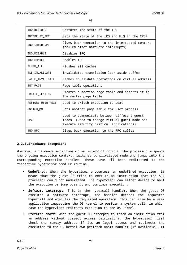
D3.2 Preliminary SPD Node Technologies Prototype nSHIELD
RE
When the Linux kernel executes a hypercall, it puts data structures, operators and other arguments to the specific hypercall in the ARM registers R0-R1 while R2 is reserved for the hypercall number. The SWI handler then interprets these parameters.
It’s also important that user processes can run on the Linux kernel unmodified, maintaining binary compatibility. This is achieved by reserving all the original system call numbers from Linux in the hypervisor. When the user process uses the library to use the system calls, which is done through a SWI instruction, the hypervisor SWI handler catches this and forwards the call to the Linux kernel with the correct virtual guest mode where it will be processed. When it is finished with the kernel operation, it gives back execution to the hypervisor that in turn restore the context of the user process that used the system call.
There are also some important security checks in these handlers checking if the hypercall originated from the correct address space, such as that user space can never execute hypercalls that is intended for the kernel. Another important thing is that if a pointer is passed to the hypervisor, it needs to make sure that the process executing the call owns the memory address of the pointer. It would be a security hole if it were possible to pass arbitrary memory address and the hypervisor blindly writes to the given parameter. Currently, we check the virtual address of the running process along with the active virtual guest mode. If the virtual address is smaller than 0xC0000000, it belongs to user space, and above 0xC0000000 belongs to kernel, except the first MB from 0xF0000000, which is the hypervisors virtual address space.
2.2.5.5 Linux Kernel Integrator Platform
Normally the platform setup is performed in the start of the Linux kernel; it is now being setup by the hypervisor initialization and is not executed in the Linux kernel. Only the relevant data structures and device operations are kept to maintain normal functionality. The platform IO has been setup to use the following mappings.
Table 2-6: Integrator CP platform IO
Virtual Physical Device
0xF100 0000 0x1000 0000 Core module registers
0xF110 0000 0x1100 0000 System controller registers
0xF120 0000 0x1200 0000 EBI registers
0xF130 0000 0x1300 0000 Counter/Timer
0xF140 0000 0x1400 0000 Interrupt Controller
0xF160 0000 0x1600 0000 UART 0
0xF170 0000 0x1700 0000 UART 1
0xF1A0 0000 0x1A00 0000 Debug LEDs
0xF1B0 0000 0x1B00 0000 GPIO
The IO has been setup by the hypervisor and complies with the virtual addresses of Linux.
2.2.5.6 Summary
The Linux port is still ongoing work and in this phase of development, it’s still too early to present a prototype. However, foundation of the port is in place and we have gotten as far as the kernel has successfully passed all boot and architecture initialization, exception handlers are connected through the hypervisor, major part of the hypercalls and system are paravirtualized and the scheduler has started the first user process. As the memory management is quite complex in the Linux kernel, we have to go
D3.2 RE
Page 32 of 70 Issue 5

nSHIELD D3.2 Preliminary SPD Node Technologies Prototype
RE
through extensive debugging and tests in order to make sure that it works as intended, especially the user processes running in the system.
When we have managed to get the bash shell command up and functioning, the next step is then to put the ported OS through extensive system tests and benchmarks to be sure that it’s stable and dependable.
2.2.6 References
1. K. Stammberger "Current trends in cyber-attacks on mobile and embedded systems", Embedded Computing Design, September 2009. Available: http://embedded-computing.com/current-trends-cyber-attacks-mobile-embedded- systems
2. Gerald J. Popek and Robert P. Goldberg. Formal requirements for virtualizable third generation architectures. Commun. ACM, 17:412–421, July 1974.
3. VMware. Understanding full virtualization, paravirtualization and hardware assist. http://www.vmware.com/files/pdf/VMware_paravirtualization.
4. ARM Security Technology. Building a secure system using trustzone technology. http://infocenter.arm.com/help/topic/com.arm.doc.prd29-genc-009492c/PRD29-GENC-009492C_trustzone_security_whitepaper.pdf, 2005-2009.
5. ARM. Virtualization is coming to a platform near you. http://www.arm.com/files/pdf/System-MMU-Whitepaper-v8.0.pdf, 2010-2011.
6. Robert Kaiser. Applicability of virtualization to embedded systems. In Massimo Conti, Simone Orcioni, Natividad Martínez Martínez Madrid, and Ralf E.D. E. D. Seepold, editors, Solutions on Embedded Systems, volume 81 of Lecture Notes in Electrical Engineering, pages 215–226. Springer Netherlands, 2011. 10.1007/978-94-007-0638-515.
7. Joo-Young Hwang, Sang-Bum Suh, Sung-Kwan Heo, Chan-Ju Park, Jae-Min Ryu, Seong-Yeol Park, and Chul-Ryun Kim. Xen on arm: System virtualization using xen hypervisor for arm-based secure mobile phones. Communications Society, pages 257–261, 2008.
8. Rafal Kolanski and Gerwin Klein. Formalising the l4 microkernel api. In Proceedings of the 12th Computing: The Australasian Theroy Symposium - Volume 51, CATS ’06, pages 53–68, Darlinghurst, Australia, Australia, 2006. Australian Computer Society, Inc.
9. C. Gehrmann, D., Heradon and K.D. Nilsson, Are there good Reasons for Protecting Mobile Phones with Hypervisors? In: IEEE Consumer Communications and Networking Conference, 9-12 Jan 2011, Las Vegas, Nevada, USA.
10. ARM Architecture Reference Manual ARMv7-A, http://www.lcs.syr.edu/faculty/yin/teaching/CIS700-sp11/arm_architecture_reference_manual_errata_markup_8_0.pdf
11. Communications of the ACM. Interview with steve furber. http://cacm.acm.org/magazines/2011/5/107684-an-interview-with-steve-furber/ fulltext, 2009.
12. Open Virtual Platforms, www.ovpworld.org
13. Linux Kernel ARM page table, http://lxr.free-electrons.com/source/arch/arm/include/asm/pgtable.h?v=2.6.34;a=arm
14. Linux Kernel ARM memory layout, http://www.kernel.org/doc/Documentation/arm/memory.txt
RE D3.2
Issue 5 Page 33 of 70

D3.2 Preliminary SPD Node Technologies Prototype nSHIELD
RE
2.3 Secure ES firmware [T2data]2.3.1 Description
The prototype hardware is based on the jointly selected BeagleBone platform which includes an AM3359 processor (ARM Cortex-A8). The BeagleBone development kit is shipped with software including a boot loader and Linux. The actual boot loader is UBOOT and it lacks some properties for required by nSHIELD. There is no integrity control of the images to be loaded; the footprint of the final image exceeds the internal static ram inside the ARM processor (which has resulted in a two stage boot procedure). Finally the code base is licensed under the restrictive GPL license. Therefore a new design has been selected in favour of modification of UBOOT. The high level requirement from nSHIELD to apply SPD Metrics on the firmware must be addressed in the design. Since the final design goal is to provide a ROM code inside the ARM processor the dependency of other nSHIELD components is not applicable. Privacy depends on integrity. General security metrics could be mapped to properties of cryptography such as selected algorithms and key length, however security also depend on the quality of the implementation, therefore the design is made for review. The design enlightens the execution path from power-on until control is passed to the loaded and verified image. The flexibility of Uboot is provided by parsing custom boot scripts; in the new design one static boot flow applies restrictions, but enables improved security instead. Flexibility is however provided by the layout of the image, since it contains different objects such as executable, ram disk and parameter blocks. Each object in the image is cryptographically sealed. The parameter block enables allocation of loaded objects in memory as well as passing parameters to the object prior to execution.
The first software that executes after a power-up or a reset is secloader. The name indicates that this is prototype and not implemented inside the ARM processor. The functionality of secloader can be visualized with the following flow chart:
D3.2 RE
Page 34 of 70 Issue 5

nSHIELD D3.2 Preliminary SPD Node Technologies Prototype
RE
Figure 2-9: Secloader functionality
When the system is started, secloader first initializes hardware and starts the watchdog. After this, a normal power-on-self-test should be performed.
When the power-on-self-test has executed, secloader checks if a secondary boot media (USB stick) is present. Before booting from the USB stick, secloader checks how many times it has previously tried to boot from the USB stick. For each attempt, the dirty_external parameter is incremented by one. If this parameter reaches max_external, secloader no longer tries to boot from the USB stick. Instead, it attempts to boot from the primary media.
When booting from USB, secloader searches for an image on the USB stick. To verify the images, secloader uses the public part of the key, which is stored on the board. If secloader fails to authenticate the images, external boot is aborted and secloader tries to boot from internal media. If the images are correctly verified, secloader increments the dirty_external parameter and extracts them to internal RAM. After this is done, the extracted and verified image is started.
If no USB stick is detected, secloader attempts to boot from the internal media. As is the case when booting from USB, secloader checks how many times it has tried to boot from internal media by verifying
RE D3.2
Issue 5 Page 35 of 70

D3.2 Preliminary SPD Node Technologies Prototype nSHIELD
RE
and thereafter incrementing the dirty_internal parameter. If the parameter reaches max_internal, secloader no longer tries to boot from compact flash.
When booting from compact flash, the image is located on the first partition of the media. If secloader fails to authenticate the image, internal boot is aborted and secloader performs a hard reset of the board. If the images are authenticated, they are extracted to internal RAM and started in the same way as for USB.
If both primary and secondary media are corrupt i.e. both dirty_internal and dirty_external have reached their respective max-values, dirty_external is set to zero before the board is reset.
2.3.2 Architecture Modules
The secure firmware is based on a fixed boot flow that enables addition of cryptographic functions for verifying issuer of images to be loaded. The implementation of the prototype is written mainly in portable C with a few exceptions:
• Low level hardware access
• CPU mode and cache
• Stack management
The resulting firmware image is monolithic but is based on several modules. The execution path involves two modules:
• bios_low (memory and hardware setup)
• bios_high (static boot flow logic)
The first instruction in the bios_low module is placed on address 0x402F0400 in the processors physical address space. The last instruction is a call to bios_high. In between a full C environment is established so that code generated by a standard C-compiler could be used for all functions in bios_high. To allow flexible memory configuration the new design will adopt Serial Presence Detection. Normally a memory module has a small i2c module containing all sizing and timing parameters needed for memory controller configuration. The prototype will use the i2c memory located on the motherboard to simulate a memory module. The static specific memory configuration will be replaced with a standard SPD detection similar to X86 based systems.
The remaining modules are:
• bios_timer: timing function library and hardware setup
• i2c_driver: management of devices on i2c bus
• bios_mmc: media controller (SD card)
• bios_output: output on serial port
• plf_bios_arm: minimal portable C-library
• provision: cryptographic library
• bios_vfat: file system library
• bios_usb: usb stack for storage type device
2.3.3 Architecture Interfaces
2.3.3.1 Passing SPD Metrics
The firmware is responsible of configuring SDRAM and then report the size of memory to the object that will be loaded and executed. For ARM processors a data structure in memory holds this information. By
D3.2 RE
Page 36 of 70 Issue 5
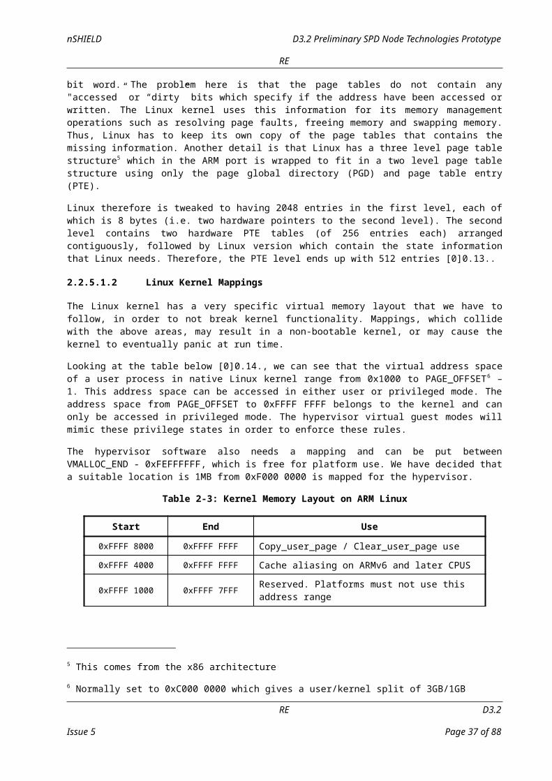
nSHIELD D3.2 Preliminary SPD Node Technologies Prototype
RE
adding a new type to the ATAG-list, SPD metrics could be passed from the firmware to next layer of software (Linux / hypervisor).
2.3.3.2 Load Image Format
Figure 2-10: Load image format
struct linux_kernel { int load_address; int start_address; char cmdline[1024];};
struct hypervisor { int load_address; int start_address; char cmdline[1024];};
typedef union { struct linux_kernel; struct hypervisor;} item;
typedef struct object { int type; item data; int object_start; int object_len; int object_signature_type; int object_signature_start; int object_signature_len; };
2.3.4 Boot Media Layout
By dividing the boot media into partitions and optionally keep the boot partition read-only, the solution becomes more robust.
The production file system is located on the second partition.
2.3.5 Parameters Stored on the Motherboard
The parameter memory is located in a non-volatile I2C memory located on the board. It is available from secloader, and must be accessible from the next layer of software. The following parameters are stored in the parameter memory:
Table 2-7: Parameter memory contents
RE D3.2
Issue 5 Page 37 of 70
Object 1 OBJECT 2 OBJECT 3
HEADER DATA SIGNATUR
E

D3.2 Preliminary SPD Node Technologies Prototype nSHIELD
RE
Name Description
Serial The serial number written during production of the unit.
Boot key The public part of the key used to verify images to load.
ATB Attempt-to-boot flag.
dirty_internal A parameter indicating how many times secloader has tried to boot from compact flash.
max_internal The maximum number of internal media boot attempt permitted.
dirty_external A parameter indicating how many times secloader has tried to boot from USB.
max_external The maximum number of USB boot attempt permitted.
The parameter memory has a CRC that guarantees that the data is not corrupt. If the CRC is not correct, secloader initiates the parameter memory to default values.
2.3.6 Metrics
SPD Values:
• The firmware resides inside the silicon of the ARM processor (last phase in design document) and dependencies to other nSHIELD components are therefore not applicable. Code quality is subject to analyse, other metrics include code size, complexity, test coverage etc.
Dependability:
• Not applicable
Privacy:
• Not applicable
Security:
• Code Quality 1-255
• Strength of cryptographic algorithms 1-255
• Length of cryptographic keys 1-255
SPD Metrics will be passed as ATAG list element.
2.4 Power Management & Supply Protection Technology [AT]2.4.1 Description
Power management and supply protection is fundamental feature to ensure the reliability of any electronic device. The technology under development uses commercial available power management semiconductors to integrate their features into nSHIELD networks
2.4.1.1 Technology Architecture
The first step has been the definition of reference architecture for the power management & supply protection unit as show in Figure 2-11. This power unit is referenced from here on as the Smart Power Unit (SPU). The following sub-modules can be identified in the SPU:
D3.2 RE
Page 38 of 70 Issue 5
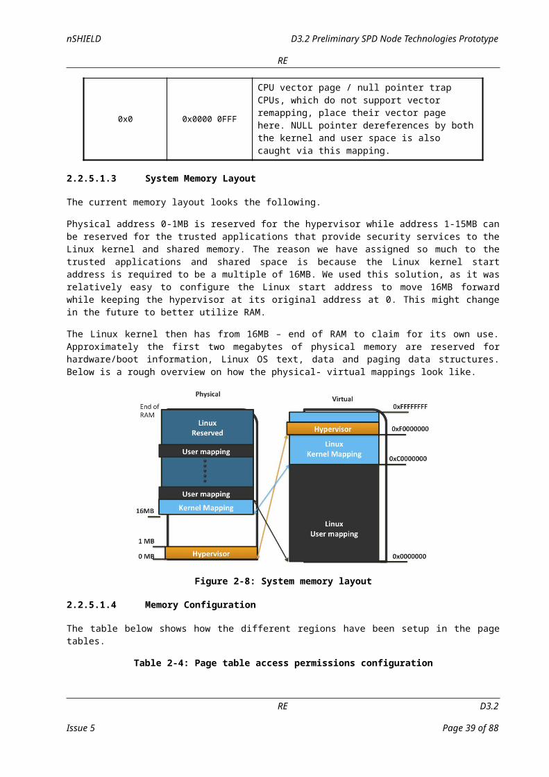
nSHIELD D3.2 Preliminary SPD Node Technologies Prototype
RE
• Power Inputs: Include all the power sources AC/DC and they can be of different types: power line / harvesting / battery …
• Power Outputs: Include all the power sinks and will be mainly DC in the 3.3V to 12V range.
• Input Hardware Modules: Embed the needed semiconductors to adapt the input power sources to the battery module.
• Microcontroller (µC): Includes an ARM low power microcontroller that manages the SPU and implements its needed functions and external/internal interfaces. The following SW/HW have been identified:
o Input Manager: Manages the input hardware modules.
o Output Manager: Manages the output hardware modules.
o Command & Control Manager: Implement the command and control interfaces that allow the integration of the SPU with other nSHIELD modules in order to compose the nSHIELD node. Currently standard serial HW interfaces have been proposed (SPI or RS232).
o Modes Manager: Different power modules manager to implement different power states for the SPU (standby, sleep, low power, normal mode…).
o Monitoring Manager: Implements the monitoring of the different HW modules of the SPU. The monitored parameters are accessible externally over the C&C interface.
o Alarms Manager: Implements the alarm configuration and triggering for the monitored parameters.
o Battery Manager: Manages the battery hardware.
• Output Hardware Modules: Embed the needed semiconductors, mainly linear regulators, to provide several output voltage signals. This module support programmable output voltages with different maximum output currents to supply different modules.
• Batteries: Embed all the power storage devices.
o Bypass: Module that bypass the input power signal to the output power modules for scenarios with no battery units.
o Battery 1, 2…N: One or more battery devices that provides energy storage.
RE D3.2
Issue 5 Page 39 of 70

D3.2 Preliminary SPD Node Technologies Prototype nSHIELD
RE
Figure 2-11: Smart power unit
The parameters/attributes that have been identified to define the SPU features and current state are:
• C&C manager:
o firmware version,
o SPU name,
o serial configuration,
o authentication parameters,
• Input: number of inputs. For each input
o enable/disable,
o type (Harvesting, Power Line),
o frequency (DC, AC (frequency))
• Output: number outputs. For each output
o enable/disable
o DC voltage (range)
• Battery Manager: For each battery
o enable/disable,
o capacity,
o load (%),
o estimated autonomy,
• Monitoring:
o inputs voltages/currents,
o output voltages/currents,
D3.2 RE
Page 40 of 70 Issue 5

nSHIELD D3.2 Preliminary SPD Node Technologies Prototype
RE
o temperature, humidity
• Alarms:
o alarm status (related to timestamp if possible):
Batteries alarms: Battery Low, Overload, Over Temperature, Input/output over limits
Input/outputs alarm: Current threshold overrun
2.4.1.2 Technology Prototype
The previous section describes a general SPU that could not be very energy efficient to implement for specific input/output power signals. In order to develop more energy efficient and simple SPU several more specific devices are planned. The final selection will depend on the requirements and needs of the components that will use this module:
• DC/DC SPU: Power management and supply protection for DC (12V-25V) to DC (3.3V-5.0V)
• AC/DC SPU: Power management and supply protection for AC (220V-50Hz) to DC (12V-25V)
• DC/DC SPU+: Same features of the DC/DC SPU but includes a battery unit.
• AC/DC SPU+: Same features of the AC/DC SPU but includes a battery unit.
All the above SPU include the full implementation of the C&C interface and all the µC internal modules depicted in Figure 2-11.
2.4.2 Architecture Modules and Interfaces
Deliverable D2.4, done in the scope of WP2, defines a set of basic functionalities at node layer in order to support the final composition of capabilities in nSHIELD framework.
In this section, a preliminary design of a power unit has been presented. This unit could be mapped directly as one of the modules, “power module”, defined in the node layer of nSHIELD device. Figure 2-12 summarized node layer modules described in D2.4.
Figure 2-12: nSHIELD Reference architecture – Node Layer (power module)
Taking into account the description of the node layer modules done in the architecture definition, this module should provide some attributes in order to be monitored by other components in nSHIELD architecture.
The components and attributes defined for the power module in the reference architecture are summarized in the following table:
RE D3.2
Issue 5 Page 41 of 70

D3.2 Preliminary SPD Node Technologies Prototype nSHIELD
RE
Table 2-8: Power module at node layer
Attributes
Power module
Mode Low power
Source Power line Battery Energy harvest AC DC
Protection Fuse
All of these attributes could be monitored by the monitor module of nSHIELD node, but this internal interface needs to be defined. SPI or RS232 could be the best options.
Taking account that the definition of the reference architecture proposed at this moment is an intermediate version, the components and attributes can be modified and completed.
Some attributes that could be monitored in order to provide interesting information about the operation of the module would be: inputs voltages/currents, output voltages/currents, temperature, and humidity. But these attribute would be better defined during the final design of the module, taking account that this is only a preliminary version of the module that need to be discussed with other partners in order to build an useful nSHIELD module.
2.4.3 Metrics
In the same way that D2.4 describes an intermediate version of the reference architecture of nSHIELD system, D2.5 defined the preliminary metrics that nSHIELD system should provide. This preliminary definition of the metrics is split by layer.
The main metrics that can be provided by the module descript in this section are related with the availability, the code execution, the data freshness, and the alternative power supply sources. Also metrics like low power mode would be provide if it is required.
2.4.4 References [Optional]
15. http://www.ti.com/lit/an/snva630/snva630.pdf
16. Supply Protection Controller: http://www.linear.com/product/LTC4365
17. Supervisory Circuits: http://www.maximintegrated.com/datasheet/index.mvp/id/5842
18. Power modules: http://www.ti.com/product/pth05050w
D3.2 RE
Page 42 of 70 Issue 5

nSHIELD D3.2 Preliminary SPD Node Technologies Prototype
RE
3 Micro/Personal Node [ETH]The main research areas targeted by the micro/personal enabled node technologies are the following:
• Trusted ESs based on Trusted Platform Module or Smartcard.
• Easy and dependable interfaces with the sensors focusing on the implementation of protocols for wireless node which don’t need to remain constantly in active mode, optimizing power consumption.
• Advanced biometric algorithms that are capable to identify the most significant features of the face and of the voice of a person.
XXXXXXX TO BE COMPLETED XXXXXXXXXXXX
3.1 Access Rights Delegation [Telcred]Within the scope of 3.2 (WP3, Task 2) an approach to delegation of access rights has been investigated. In a network of offline trusted embedded systems, a node need to be able to authenticate another node requesting some privileges, but also to determine what – if any – privileges should be granted. A model for doing this has previously been developed by the project partner (Telcred), but this model assumes that all access rights are issued by a central trusted authority and does not support delegation.
A real world example where delegation of access rights would be relevant is where the access rights issued by the central authority are valid only if the node seeking access has first interacted with another node. For example node: “Allow access to door B, but only if the visitor has first passed door A”. In this example, door A is entrusted to verify that a correct passage has taken place.
The approach that was investigated uses a construct called a path array. Nodes to which some authority has been delegated can read and write to the path array, thereby proving that a bona fide interaction has taken place. This information can then be used by the next node in the path array as part of the access control decision.
The work was mainly carried out as a M.Sc. thesis at KTH, the Royal University of Technology in Stockholm.
3.1.1 Problem Statement
In an offline PACS (Physical Access Control System), there is no continuous exchange of information to verify and allow a user through a series of doors, whereas this is a common feature in an online PACS. Current offline systems are unable to force a user to follow a certain designated route, e.g. Room A should be accessed before entering room B. This project explores a model to enforce such a route, by using delegation of some authority from the main administrative system to the offline locks.
3.1.2 The Concept of “Path Array”
The developed artefact consists of a construct known as Path Array aka PA. Path Array is an array that can be one or multi-dimensional based upon the administrator requirements. PA consists of Lockid stored into each index of the array that needs to be accessed by the user in a sequence. Administrator is responsible to implement path array onto the user’s smart card before handing it over to the user.
Ticket that is stored in the flash memory of the smart card contains the PA. After the formation of mutual trust between the Lock and Card, Lock makes use of the remaining contents inside the Ticket for decision making.
RE D3.2
Issue 5 Page 43 of 70

D3.2 Preliminary SPD Node Technologies Prototype nSHIELD
RE
Figure 3-13: Path Array Design
The Figure above shows the outline of PA. PA consists of Lockid stored at each index (i = 0, 1, 2...). PA holds the Lockid that should be accessible by a user in a sequence. Server digitally signs the PA stored inside the Ticket. Index i value starts from 0 and increments each time a user passes a door. This index value points to the Lockid that the user needs to visit. Hence, the contents of the Ticket will be as follows.
Figure 3-14: Ticket along with Path Array
3.1.3 Mechanism of the Artefact
After the creation of trust between the entities of offline PACS, Lock now processes the contents of PA, and then checks for its own ID at the current index i, if it is found then Lock performs three steps as follows,
• Increment index i
• Generate HMAC and write it to Card
• Grant access to the user
If the Lockid present at index i does not correspond to Lock own id, it then it denies the access and logs the user action.
3.1.3.1 Incrementing Index i
The path array PA contains lock ids stored inside it. Only the relative matching Lock is allowed to increment i value by one. At the time of generation of Ticket by the Server, it also generates a HMAC to be used by the first lock in the PA. The Lock located at the first index of PA makes use of this HMAC to ensure that no illegal modifications are done on the smart card. The Index of PA starts from the value 0. For instance, consider the below path array. This path array consists of lock ids B, A and C which should be followed in that order by the user.
D3.2 RE
Page 44 of 70 Issue 5

nSHIELD D3.2 Preliminary SPD Node Technologies Prototype
RE
Figure 3-15: Ticket Incrementing the index value
In the figure above, the current value is 0 and PA[0]=B. Only the lock with id ‘B’ can increment the i value further.
3.1.3.2 Generating Hash using HMAC
Lock creates the HMAC after incrementing the i value. HMAC stands for Hash Based Message Authentic Code. It calculates the message authentic code using a cryptographic hash function and shared secret key. In the offline PACS scenario, geographically dispersed locks securely exchange the messages among them by using message digest. HMAC is necessary in offline PACS scenario to ensure the integrity of smart card contents. The process of creating HMAC is as shown in the formula below.
where:
• K is the shared secret key
• m is the message to be protected
• opad is outer padding (0x5c5c….)
• ipad is inner padding (0x3636….)
• H is the cryptographic hash function (MD5, SHA etc.)
• || is concatenation
• is the exclusive-OR operation
The locks inside the facility were pre-installed with keyshared. Concatenating the keyshared with Lockid
generates the secret key keysecret. Message m in this context indicates the current index i value, and the rest of them use default parameters.
While hash generation, keysecret = keyshared || Lockid.
Generation of HMAC is as following:
RE D3.2
Issue 5 Page 45 of 70
i = 0

D3.2 Preliminary SPD Node Technologies Prototype nSHIELD
RE
Figure 3-16: Process of HMAC creation
In the above figure, H can be any hash algorithm.
3.1.3.3 Generating Hash by the Locks in the Sequence
The overall concept of the artefact is to enforce the user through the path specified by the administrator. The user should attend this path in sequence. Hence, if one lock grants access to the user, which is present at index zero of PA i.e., PA[0], then the next lock in the sequence, which is available at PA[1] should be able to prove that the user has already passed through the door mentioned at PA[0].Verification of the hash value generated by the lock present at PA[0] solves the above issue.
When the user presents his smart card at a Lock mentioned in the PA, the lock allows access only if it has confirmed that the user has already been allowed access by an earlier lock. During the verification process of HMAC Lock always uses the previous index for key generation and while in a hash generation process it uses its own Lockid. Current lock initially checks i value.
3.1.3.3.1 Scenario 1: If i=0
Then the lock knows that it is the first lock in the order. It then checks whether the value present at PA[0] matches its own lock id. If the id is not equal to its own id, it will log the user activity and deny the access.
Lock has the authority to perform further actions if the value at PA[0] matches its own id. It then verifies the HMAC stored by the Server on the Card, to make sure that nothing has been changed illegally. It will then increment i value by one and will generate HMAC by using the secret key keysecret. In this scenario, keysecret results from concatenating the keyshared with its own Lockid.
3.1.3.3.2 Scenario 2: If i>0
If i value is greater than zero, then lock confirms that the user has already accessed some doors in the sequence. Hence, it will confirm its own authority that it can change the contents of the card by looking up
D3.2 RE
Page 46 of 70 Issue 5

nSHIELD D3.2 Preliminary SPD Node Technologies Prototype
RE
for its own lock id, and then generates hash to verify the hash stored by the earlier lock. Now, the Lock increments i value by one and generate a new hash to be used by the next lock in the series.
Verification steps by current lock in action are as follows,
• Step 1: reads current i value
• Step 2: Looks up present at PA[i]
• Step 3: If the value of own =PA[i], then proceed to step 4 else go to step 10
• Step 4: Verify the HMAC hash stored on smart card (generated by previous lock)
• Step 5: If the hash can be verified, continue else go to step 10
• Step 6: Increment i value by one
• Step 7: Generate new HMAC
• Step 8: Replace the old HMAC with generated HMAC to be used by next lock
• Step 9: Allow access and stop
• Step 10: Deny access and log user activity onto the card
Using above procedure the nth lock will verify that the user has accessed the (n-1) th lock, and this process continues with all the locks.
3.2 References19. Sivakumar Tati, B. (2012). A framework to implement delegation in offline PACS. M.Sc.
degree thesis. KTH, Sweden.
RE D3.2
Issue 5 Page 47 of 70

D3.2 Preliminary SPD Node Technologies Prototype nSHIELD
RE
4 Power Node [ISD]The main research areas targeted by power node technologies are the following:
• Audio based surveillance.
• Avionic system.
• Integration of heterogeneous embedded systems.
• Solutions for support of PN ???
• TPM support ????
XXXXXXX TO BE COMPLETED XXXXXXXXXXXX
4.1 Audio Based Surveillance [ISD]4.1.1 Description
4.1.1.1 Introduction
ISD has been designing a novel audio based surveillance system that aims to overcome the most important limitations of non-military grade systems currently utilized in acoustic based research by providing correlated data acquisition from a large number of overlapping sensors.
Its hardware synchronized sensors make it ideal for applications requiring 3D sound capture such as acoustic hologram generation in real time. It features an extremely flexible and high performance DMA engine able to perform any type of spatial processing purely in hardware. It will be the only system able to deliver to main memory synchronized uncompressed audio streams from up to 768 microphones with zero CPU load. Its hierarchical structure is fully extensible and able to support any number of microphones. The targeted implementations will support from 8 up to 768 sensors in multiples of 8 units.
4.1.1.2 System Boards
The system consists of 3 types of boards, namely the audio daughterboards, the concentrator boards and the grabber board.
The audio daughterboard, which has already been manufactured and tested, is used in order to receive audio streams from up to eight microphones, perform amplification of the audio signals and analogue to digital conversion. It supplies the combined digital audio stream to the concentrator board, on which it is plugged.
D3.2 RE
Page 48 of 70 Issue 5

nSHIELD D3.2 Preliminary SPD Node Technologies Prototype
RE
Figure 4-17: The audio daughterboard
The concentrator board is equipped with 16 input slots, where audio daughter boards can be plugged into. It is also equipped with a single output UTP port, able to deliver the combined audio streams to the grabber board. The concentrator board design is currently in progress.
Finally, the PCIX grabber board is equipped with 6 input UTP ports where concentrator boards can be connected using standard UTP cat6 network cables. It receives the streams and delivers the data to the host utilizing an extremely powerful and flexible DMA engine.
Figure 4-18: The grabber board
The grabber board hardware is available and its firmware is currently under design.
4.1.2 Architecture Modules and Interfaces
4.1.2.1 Power
Due to the inherent redundancy of the architecture, no power protection countermeasures need to be taken. Each of the concentrator boards will be independently powered and will supply power to the daughterboards plugged to it. Thus cutting off power to one of the concentrator boards will not affect the system at all provided that we deploy a topology utilizing overlapping sensors attached to different concentrators. As more concentrators get powered off, the system performance will start degrading as soon as all sensors deployed in a region belong to concentrators that have been powered off.
Moreover, the grabber board is bus powered, thus its availability regarding power depends on the power availability of the embedded PC it is attached to.
4.1.2.2 Security
Due to its nature, the system can be utilized as an anti-tampering mechanism by examining in real time the audio signals captured by sensors that are attached to its components. Moreover the communication between the concentrators and the grabber will be encrypted to guarantee data integrity. Code integrity is ensured by making the design non-upgradeable in the field. Finally, data freshness will be ensured by attaching a monotonically increasing label to each chunk of data captured.
4.1.2.3 Status and Configuration
The node will inform upper layers regarding its status (detection of tampering attempt, sensors activated) and will allow them to configure the sensors to activate.
4.1.3 Metrics
The node will provide metrics on its availability, tamper resilience and data freshness computed at real time as well as Boolean metrics describing its capabilities (such as ability to reconfigure the sensors utilized).
RE D3.2
Issue 5 Page 49 of 70

D3.2 Preliminary SPD Node Technologies Prototype nSHIELD
RE
4.2 System of Embedded System - SoES [SESM]4.2.1 Description
This section illustrates the technologies that will be employed to develop the power node prototype.
Leveraging the results gained on pSHIELD and considering the current evolution of nSHIELD, we began an in-depth analysis geared towards the identification of technologies that shall ease the composability of heterogeneous SHIELD nodes.
The selected technologies will be used to endow SPD functionalities to legacy systems that, because of their nature, are not SHIELD compliant. In particular, we envision applying the aforementioned results to an Avionic System. Due to the fact that avionic systems are dominated by very stringent security policies, the integration of nSHIELD in such environment is extremely challenging and valuable.
So far, a subset of technologies has been identified and some of them verified. Once the set of the technologies will be consolidated the integration process will be triggered. The result of such integration will be an IP that will expose the following features:
• Monitor interface;
• Data integrity;
• Encryption / Decryption;
• Dynamic Reconfiguration (complete and partial);
• Abnormal event detection;
• Diagnostic.
The process of technologies selection and technologies integration is tightly connected to the avionic application scenario; since the application scenario has not been consolidated yet, an adaptation of the exposed features is foreseen.
More specifically, a FPGA IP will be developed, according to the nSHIELD Overall Architecture as depicted in D2.3. It will represent an nS-ESD GW (nSHIELD Embedded System Device Gateway) that will provide enhanced capabilities in terms of security and dependability to the cluster where it will be integrated.
D3.2 RE
Page 50 of 70 Issue 5

nSHIELD D3.2 Preliminary SPD Node Technologies Prototype
RE
Figure 4-19: nS-ESD GW Integration
As shown on the picture above reported, the FPGA-based IP will operate as an nSHIELD adapter that interconnects the middleware and the node layers. To achieve the dependability and to assure performances, a Softcore microprocessor will be synthesized onto FPGA to support the application-specific customization. The implementation of the aforementioned IP implies the development of custom hardware controllers and software drivers, because of the heterogeneous nature of legacy nodes.
The overall IP design process will be performed in adherence to the RTCA/DO-254 and RTCA/DO-178B standard.
4.2.2 Architecture Modules and Interfaces
As reported by the Node Layer Logical View depicted in the D2.4, the FPGA-based IP Core will include different modules to implement specific capabilities.
Figure 4-20: IP Logical Architecture.
As shown in the picture above, the internal outlined architecture consists of a set of different components whose synergy will foster the integration of legacy embedded systems in the SHIELD architecture. According to the logical view of the FPGA-based IP Core, the modules that will be developed are the following:
• Monitor module;
• Coordination module;
• Security module.
More specifically, in the context of this partitioning it’s possible to identify elements that are involved to implement security, communication and monitoring functions.
4.2.2.1 Monitor Module
In order to foster the integration and communications between legacy power Node and SHIELD components (Middleware, Nodes, etc.), two FPGA controllers will be developed. In the logical view above these controllers are identified as middleware and physical. Through the middleware controller the IP Core converts a service request from the nSHIELD component to a logical format that legacy systems in the lower layer can understand. This component can be seen as an interface to the SHIELD architecture. Likewise, the physical controller will be used to supply proxy services for nodes with a non-standard physical communication. According to this, it can be seen as an interface to the legacy embedded systems.
RE D3.2
Issue 5 Page 51 of 70

D3.2 Preliminary SPD Node Technologies Prototype nSHIELD
RE
Middleware and physical controllers will provide configuration and status services through both hardware and software.
4.2.2.2 Coordination Module
The presence of a softcore provides coordination capabilities. In the context of an FPGA-based solution it is possible to implement different microprocessors using logic synthesis. Different softcores can be instantiated on the FPGA according to the specific technology that will be identified to be used for the demonstrator and to specific features required. Some of softcores that can be used are:
• Microblaze: 32bit RISC-based proprietary soft-processor by Xilinx;
• Nios II: 32bit RISC proprietary softcore by Altera;
• Leon3/4: 32bit open source soft-processor based on SPARC V8 RISC architecture by Aeroflex Gaisler;
• Cortex M1: 32bit RISC ARM proprietary processor licensed by ARM Holdings;
• OpenSPARC T1: 64bit open source softcore RISC architecture by Oracle.
Thanks to the softcore it will be possible to manage the resources allocation and to balance services with the aim to ensure the system reliability with a dynamic load distribution. The processor will be exploited to execute balancing algorithms, safety algorithms, etc. The development of hardware accelerators (HA) is foreseen. An HA is a hardware implementation of a specific operation or function e.g. cryptography. There are several algorithms and functions that are specially tailored to be executed by an HA rather than a microprocessor due to their parallel nature. Using the HA is possible to optimize the system performance in a way that is not possible with traditional off-the-shelf processor.
Figure 4-21: Hardware Accelerator
4.2.2.3 Security module
Several components will be developed as parts of the security module.
The component identified as DPR will be in charge of managing the FPGA configuration. The purpose of this functional block is to increase security and dependability aspects of the node allowing the device to change between different operational modes. Thanks to this component it will also possible to run multiple applications on the same device enhancing the dependability and redundancy.
A Data Integrity controller will be included into the IP architecture to process data by implementing cyclic redundancy check. This component validates the content of each data packet by calculating a new CRC value and matching it to the one contained in the packet. The core also checks the ordering of the received packets by monitoring the contained sequence number in each packet.
D3.2 RE
Page 52 of 70 Issue 5
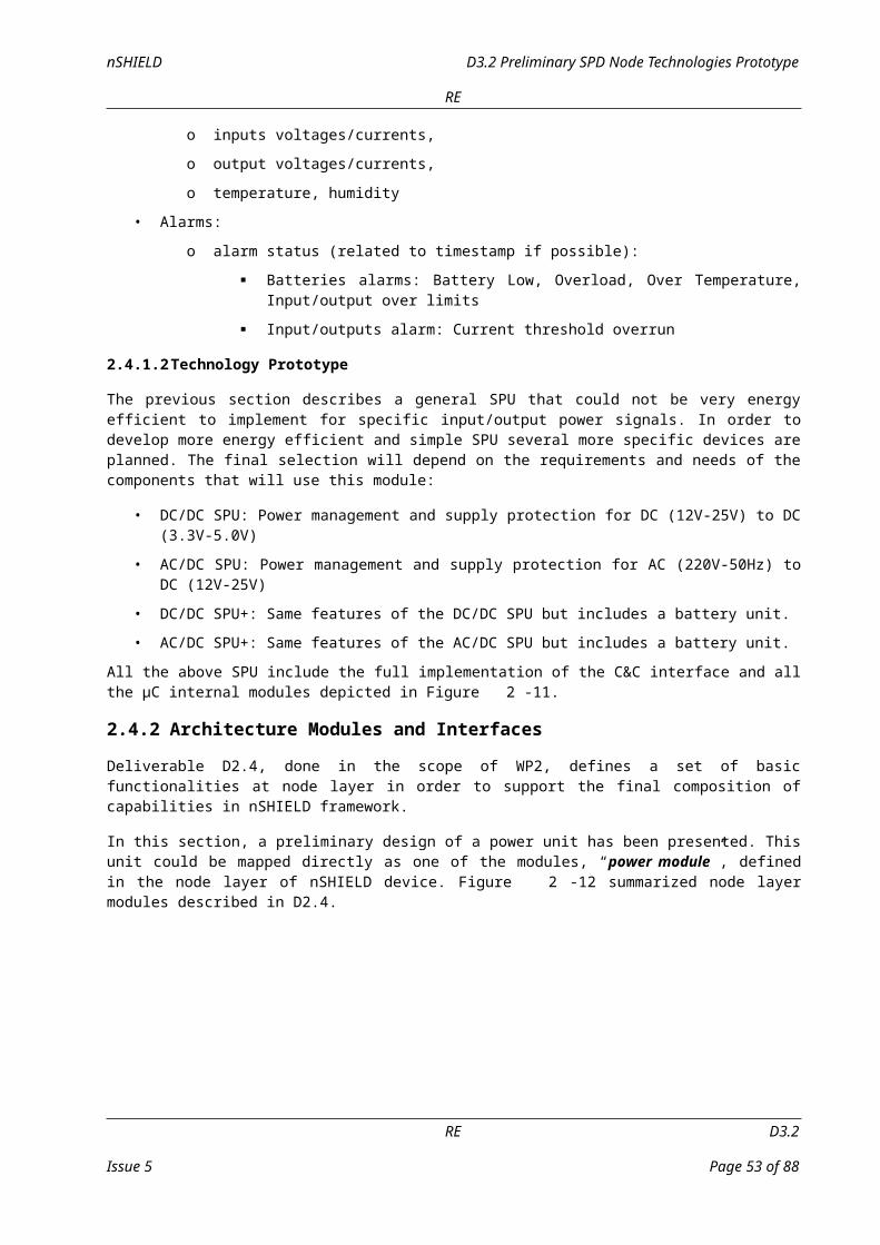
nSHIELD D3.2 Preliminary SPD Node Technologies Prototype
RE
It’s also scheduled the implementation of a Secure Storage controller to protect the confidentiality and integrity of processed data. In conjunction with a Encrypt/Decrypt controller it will be possible to ensure a long term storage of sensitive data improving security aspects of the node.
4.2.3 Metrics
The IP Core will provide metrics as defined in D2.5 (Preliminary SPD Metric Specifications). In particular, with the aim to ensure the success the integration of such IP with SHIELD architecture, security, dependability and privacy metrics will be implemented.
Digital signature policies and data freshness metrics will be implemented to confer Security aspects on the FPGA-based solution. These metrics will be implemented in the Security Module.
The runtime reconfiguration metric will be implemented to improve the Dependability of the node during either normal operation or fault conditions. This metric will be used in the DPR module.
The secure key distribution and the storage of private information will be provided to give an appropriate level of Privacy to the node. These metrics will be implemented as core of the Encrypt/Decrypt and Data Integrity controllers.
Being the node an nS-ESD GW, also node availability metric will be implemented to provide the composability of the IP inside a legacy cluster.
RE D3.2
Issue 5 Page 53 of 70

D3.2 Preliminary SPD Node Technologies Prototype nSHIELD
RE
5 Dependable self-x Technologies [UNIGE]The main research areas targeted by the dependable self-x technologies are the following:
• Mechanisms in charge of preventing non authorized/malicious people to access the physical resources of the node (automatic access control, denial-of-services, self-configuration, self-recovery, etc.).
• Self-reconfigurability and self-adaptation to guarantee robustness and dependability.
XXXXXXX TO BE COMPLETED XXXXXXXXXXXX
5.1 Platform Selection [UNIGE]According to the task requirements the research was focused to define a prototype of a scalable node family in order to cover the three node typologies and to be useful for the four application scenario.
The chosen platform integrates in a very small (18X68 mm) and low power board three main devices with different and orthogonal features: micro controller, FPGA and DSP.
The scalability can be achieved deciding which components integrate in the final product or the size of the component itself (for instance the dimension of the FPGA or the size of the microprocessor memory).
The general schematic of the prototype is shown below (source: OMBRAv2 HW MANUAL- Issue 9).
D3.2 RE
Page 54 of 70 Issue 5

nSHIELD D3.2 Preliminary SPD Node Technologies Prototype
RE
Figure 5-22: Prototype schematic
The following table summarize the prototype features (source: OMBRAv2 HW MANUAL- Issue 9).
Table 5-9: Prototype features
Description Full Version Standard Version Lite Version
Processor Ti DM3730 Ti DM3730 Ti AM3717
ARM CortexA8 processor speed 1Ghz 1Ghz 1Ghz
DSP TMS320C64+ TMS320C64+ -
DSP processor speed 800Mhz 800Mhz -
Ram POP Memory (LpDDR) 1024 Mbyte 512 Mbyte 512 Mbyte
Flash POP Memory (Nand) - 512 Mbyte -
Flash Disk On uSD card up to 32GB
On uSD card up to 32GB
On uSD card up to 32GB
Video 3D acceleration PowerVR SGX530 PowerVR SGX530 PowerVR SGX530
Wireless connection WiFi
IEEE 802.11 b/g/n (option (*))
Wireless connection Bluetooth 2.1+ EDR class 1.5 2.1+ EDR class 1.5 2.1+ EDR class 1.5
Wireless connection PAN ANT+ (option (*)) ANT+ (option (*)) ANT+ (option (*))
Wireless Bluetooth/WiFi/ANT+ antenna
Unified u.Fl connector
Unified u.Fl connector
Unified u.Fl connector
Expansions connector J1, J4, J5 J1, J4 J1, J4
USB 2.0 OTG 1 connected to ARM (HS,FS,LS)
1 connected to ARM (HS,FS,LS)
1 connected to ARM (HS,FS,LS)
USB 2.0 HOST 1 connected to ARM (HS only)
1 connected to ARM (HS only)
1 connected to ARM (HS only)
USB 1.1 HOST connected to FPGA (FS only)
connected to FPGA (FS only)
connected to FPGA (FS only)
USB 1.1 HOST/DEVICE sw configurable
connected to FPGA (FS, LS)
connected to FPGA (FS, LS)
connected to FPGA (FS,LS)
Audio Stereo Mic In, Line-in and Line-out Line-in and Line-out Line-in and Line-out
Video VGA 16 bit (VGA and XGA)
16 bit (VGA and XGA)
16 bit (VGA and XGA)
Video Digital Output connection
DSS 24 bit 1v8 levelsTV composite/S-VIDEO
DSS 24 bit 1v8 levels DSS 24 bit 1v8 levels
RE D3.2
Issue 5 Page 55 of 70

D3.2 Preliminary SPD Node Technologies Prototype nSHIELD
RE
Video Digital Input connection
Omap 12 bit Camera interface
FPGAXilinx Spartan6 (XC6SLX16-2CPG196I)
Xilinx Spartan6 (XC6SLX16-2CPG196I)
Xilinx Spartan6 (XC6SLX16-2CPG196I)
FPGA connections between FPA and OMAP
1xUSB-FS, McBSP1, McBSP4, 2xGPIO, Uart3, (2Wires), I2C-2, Uart1 (4wires), 2xGPIO
1xUSB-FS, McBSP1, McBSP4, Uart1 (4wires), Uart3/4(2Wires), 2xGPIO, I2C-2, SPI1, 6xGPIO
1xUSB-FS, McBSP1, McBSP4, Uart1 (4wires), Uart3/4(2Wires), 2xGPIO, I2C-2, SPI1, 6xGPIO
FPGA pins available for the user
4+2 on J1/J4 (1v8 IO-level)27 on J5 (1v8 IO-level)
4 on J1/J4 (1v8 IO-level)15 on J1/J4 (1v8 IO-level)
4 on J1/J4 (1v8 IO-level)15 on J1/J4 (1v8 IO-level)
Debug connectionJTAG both for processor and FPGA
JTAG both for processor and FPGA
JTAG both for processor and FPGA
Power Supply Range 3.2..4.2 Vcc, 2.5W 3.2..4.2 Vcc, 2.5W 3.2..4.2 Vcc, 2W
Temperature range (components) -40..+55 C -40..+55 C -20..+55 C
The current prototype just includes three possible levels of scalability but it is possible to build any descendent platform starting from the Full version.
The main component is the Processor and others component can be used as co-processor or as new features-hardware.
The figure below shows the picture of the OMBRA board with respect to 1 euro coin.
Figure 5-23: The OMBRA board
Hereafter the main features of the three main components of the OMBRA Board taken from the component datasheets itself: Processor, FPGA and DSP.
General feature of the chosen processor (DM3730125 Digital Media Processors):
D3.2 RE
Page 56 of 70 Issue 5
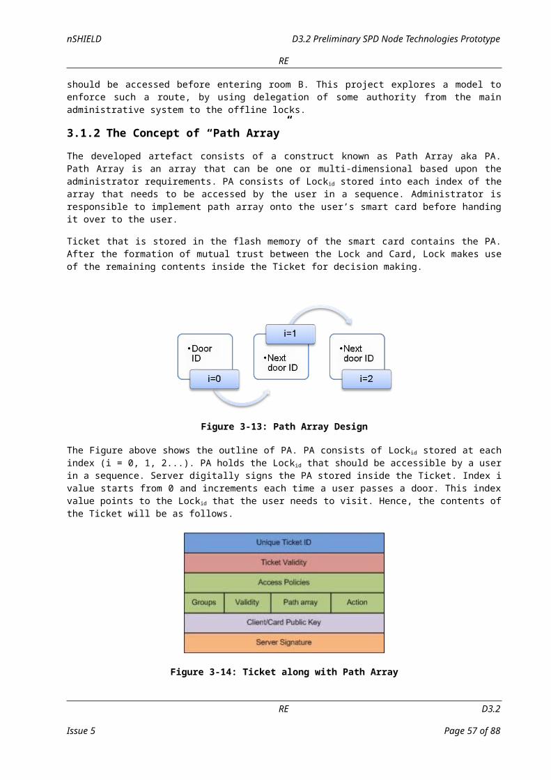
nSHIELD D3.2 Preliminary SPD Node Technologies Prototype
RE
The double boot mode, through the micro SD, allows to use the processor as a Linux or Windows CE embedded PC, with the possibility to work with the Windows or the GNU tool chain.
The selected FPGA is a Xilinx Spartan 6 – 16. All Xilinx tool chain can be used for developing HW and/or SW devices (for example a MicroBlaze was mapped on the FPGA).
RE D3.2
Issue 5 Page 57 of 70

D3.2 Preliminary SPD Node Technologies Prototype nSHIELD
RE
TMS320C64 outline:
D3.2 RE
Page 58 of 70 Issue 5

nSHIELD D3.2 Preliminary SPD Node Technologies Prototype
RE
Users and designers that want to implement self-x technologies can use the powerful reconfigurability features of the Ombra board.
For instance it is possible to change hardware functionalities reprogramming the FPGA and chaining on the fly hardware parameters or algorithms: it is possible to think that micro-controller application can reprogram the FPGA or a lot subset. It is also possible to use the FPGA IOs in order to configure different interfaces, for instance for different sensor to use in several application, maintaining the same kernel.
One of the most interesting methods for security implementation is cryptography. Several algorithms were studied and implemented; the most important point for such task is the trade-off between security level and computational complexity in order of calculation time and hardware resources.
Speaking about embedded system this kind of problem is more important with respect to the reduced size in term of area and hardware resources of the target system.
The Ombra multi-core system allows a Hardware-Software co design in a very small area, this allows to build and run algorithms as the elliptic curves cryptography in a very short time.
RE D3.2
Issue 5 Page 59 of 70

D3.2 Preliminary SPD Node Technologies Prototype nSHIELD
RE
The implemented demo shows how it is possible to run such algorithm in a very short time.
5.1.1 Metrics
The purpose of this section is to correlate the prototype features with the metrics for the node level described in the D2.5 deliverable.
Generally speaking, the prototype implements a multi core platform able to meet the requirements of self-reconfigurability and self-adaptation both software and hardware levels. Self-reconfigurability and self-adaptation are the main features in order to implement SPD capabilities also at network and middleware level. In fact, the purpose of this prototype is to provide a complete and powerful platform for not only for the three node typology but also for the upper nSHIELD levels.
Note that several metrics described in D2.5 are not directly applicable in the hardware platform but their application in the upper levels can be facilitated by an appropriate hardware platform.
5.1.1.1 Security
Metrics related to cryptography are met as demonstrated with the demo (next section). The Montgomery’s algorithm, that performs the point multiplication on an elliptic curve, is implemented in the prototype. The run speed allows using different bit lengths for the curve, allowing different security level. The possibility to use a reconfigurable hardware device could allow the application to change the cryptography parameter run time.
5.1.1.2 Dependability
The metrics of redundancy and reconfiguration can be easily achieved by the multi core platform. Redundancy is granted by the multi core and reconfiguration is granted by the reconfigurable hardware.
5.1.1.3 Privacy
The characteristics of the embedded platform ensure the possibility to store sensible and private data in non-accessible memory space. In addition an area of the FPGA (subsets of the block RAM for instance) can be allocated for this use.
5.1.1.4 Composability
The high flexibility of the node platform allows performing the listed dynamic and flexibility features.
5.1.1.5 Performance
Lightweight embedded operating system: the prototype micro-host can support Linux and windows CE.
5.1.1.6 Interfaces
The on board FPGA can be configured to directly implement custom devices or to implement connection interfaces for new devices.
5.1.2 Demo
This chapter describes the implementation on the OMBRA platform of the Montgomery’s algorithm that performs the point multiplication on an elliptic curve developed in work package 3.5, refer to section 6 for the technical details.
The target is to show the running algorithm on the implemented embedded Linux platform (Linux omap 2.6.32) and calculate the working time. It was needful to compile for the above mentioned Linux version the gnu gmp libraries.
D3.2 RE
Page 60 of 70 Issue 5
nSHIELD D3.2 Preliminary SPD Node Technologies Prototype
RE
In order to achieve a high accuracy in the running time calculation the algorithm is repeated 1000 times, dividing the final result for the repetition number. In this way we can obtain a reasonable average running time for the implemented algorithm.
Figure 5-24: Demo for 256 bit curve
We implemented the demo for two NIST standard elliptic curves: secp256r1 and secp521r1.The first curve is 256 bit length instead the second one is 521. The test program first of all asks to select the curve, and then the two branches run independently.
The figure above shows the algorithm when the 256 bit curve is selected and the one below the 521 case.
In the 256 bit length case the time to perform the point multiplication (change coordinates included) is 0.023390 seconds. In the 521 bit length case the time to perform the point multiplication (change coordinates included) is 0.113280 seconds.
RE D3.2
Issue 5 Page 61 of 70
D3.2 Preliminary SPD Node Technologies Prototype nSHIELD
RE
Figure 5-25: Demo for 521 bit curve
We perform the same experiments on an intel core i7 @3Ghz to compare the results. In the 256 bit length case the time to perform the point multiplication (change coordinates included) is 0.003895 seconds. In the 521 bit length case the time to perform the point multiplication (change coordinates included) is 0.017379 seconds. We can note that the the computational times on the OMBRA platform are very good (ratio is around 6 in the 256 bit length and around 6,5 in the 521 bit length) considering that its processor runs at 1Ghz.
D3.2 RE
Page 62 of 70 Issue 5
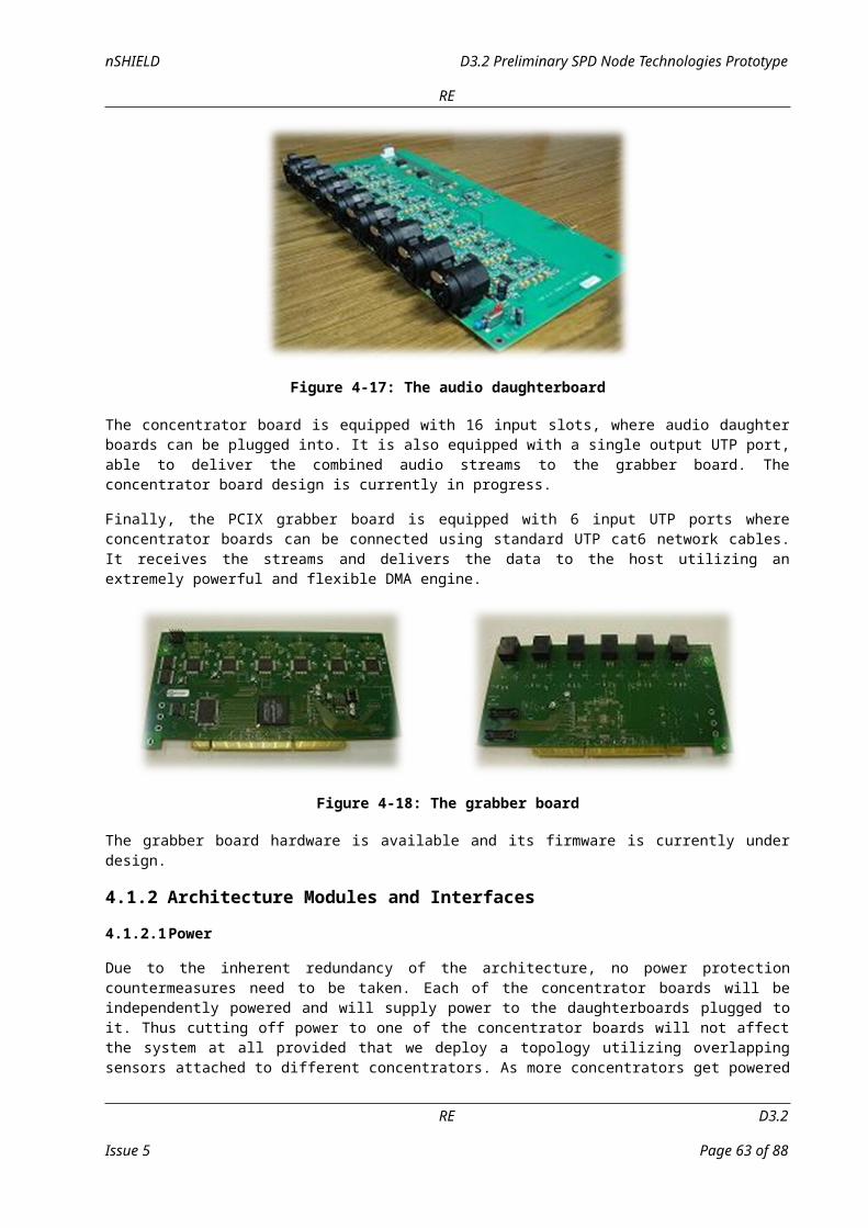
nSHIELD D3.2 Preliminary SPD Node Technologies Prototype
RE
6 Cryptographic technologies [UNIGE]The main research areas targeted by cryptographic technologies are the following:
• Hardware and software crypto technologies (including asymmetric cryptography and ECC cryptography).
• Data compression techniques combined with self-reconfiguration and self-recovery.
XXXXXXX TO BE COMPLETED XXXXXXXXXXXX
6.1 Elliptic Curve Point Multiplication over Prime Fields Library [UNIGE]
This library represents the implementation of the point multiplication operation on an elliptic curve on prime field, which is the core of elliptic curve-based cryptographic protocols like Elliptic Curve Diffie-Hellman (ECDH) and Elliptic Curve Digital Signature Algorithm (ECDSA).
Detailed information about the algorithm and the theory included in the library can be found in the deliverable D3.1.
6.1.1 Description
The elliptic curve point multiplication operation is defined as Q=kP, where Q, P are points in a previously chosen elliptic curve defined over a prime field GF(p), and k is a field element. Here p is the characteristic of the field.
The elliptic curves supported are in the simplified Weierstrass form y2=x3+ax+b, where a,b are elements of GF(p) with p different from 2 or 3. Supported curves include those specified by NIST (Standards for Efficient Cryptography 2 – September 20, 2000, available at www.secg.org) indicated as secp160r2, secp192k1, secp192r1, secp224k1, secp224r1, secp256k1, secp256r1, secp384r1, secp521r1.
This library supports elliptic curve point representations called Affine coordinates and Jacobian coordinates.
This library employs the Montgomery Ladder algorithm in order to accomplish the elliptic curve point multiplication. This is the most efficient algorithm producing side-channel attacks-resistant cryptosystems. For testing purposes only, the elliptic curve point multiplication is provided with the trivial binary method also.
6.1.2 Basic Interface
Configuration parameters: field characteristic p, elliptic curve coefficients a,b belonging to GF(p).
Input parameters: scalar k belonging to GF(p), x coordinate of the affine point P(x,y) belonging to the elliptic curve y2=x3+ax+b defined over GF(p).
Library output: if x is a valid coordinate of a point over the specified curve, the library returns the affine point Q = kP.
6.1.3 Code Compilation and Dependencies
This library requires the GNU Multiple Precision Library (libgmp) version 4.3 or higher. This dependency is freely available at http://gmplib.org, with LGPL license.
RE D3.2
Issue 5 Page 63 of 70

D3.2 Preliminary SPD Node Technologies Prototype nSHIELD
RE
The entry point of the library is represented by the source file Lib.h. A custom program including this source file can be compiled with the following line:
$ gcc -o CustomProgram CustomProgram.c Lib.c -lgmp –lm
6.1.4 Hardware platform
Hardware tests for present library are conducted on the OMBRA platform, provided by Selex ES, with a Linux operating system. This platform presents a SOIC integrating an ARM Cortex-A8 running at 1GHz.
6.1.5 Library API
void Montgomery(mpz_t x3,mpz_t y3,mpz_t x1,mpz_t y1,mpz_t field,mpz_t a,mpz_t k): performs (x3,y3)=k(x1,y1), using the Montgomery algorithm, on a curve with parameter a and over the prime field field. Point operations are performed in affine coordinates.
void Montgomery_j(mpz_t x3,mpz_t y3,mpz_t x1,mpz_t y1,mpz_t field,mpz_t a,mpz_t k): performs (x3,y3)=k(x1,y1), using the Montgomery alghoritm, on a curve with parameter a and over the prime field field. Point operations are performed in Jacobian coordinates.
int testCurve(mpz_t delta,mpz_t a,mpz_t b,mpz_t field): checks if the elliptic curve described by the parameters a,b over the prime field field is supersingular, returning delta=4a3-27b2.
int testPoint(mpz_t y_square,mpz_t a,mpz_t b,mpz_t field,mpz_t x): checks if field element x is a valid coordinate on the curve described by a,b returning corresponding y2.
int Tonelli(mpz_t c,mpz_t a,mpz_t p): given a field element a, computes c2=a mod p. Used to evaluate y from y2 provided by testPoint API.
int Hasse(mpz_t field): returns the theoretical upper bound of the number of elliptic curve points over specified field.
void KappaP(mpz_t x3,mpz_t y3,mpz_t x1,mpz_t y1,mpz_t field,mpz_t a,mpz_t k): performs (x3,y3)=k(x1,y1) on a curve with parameter a and over the prime field field. Point operations are performed in affine coordinates. This algorithm is only for testing purposes, since it makes the cryptosystem vulnerable to side-channel attacks.
void KappaP_j(mpz_t x3,mpz_t y3,mpz_t x1,mpz_t y1,mpz_t field,mpz_t a,mpz_t k): performs (x3,y3)=k(x1,y1) on a curve with parameter a and over the prime field field. Point operations are performed in Jacobian coordinates. This algorithm is only for testing purposes, since it makes the cryptosystem vulnerable to side-channel attacks.
6.1.6 Service functions
void sum(mpz_t x3,mpz_t y3,mpz_t x1,mpz_t y1,mpz_t x2,mpz_t y2,mpz_t field): sum of two elliptic curve points in affine coordinates over a specified prime field: (x3,y3)=(x1,y1)+(x2,y2)
void duble(mpz_t x3,mpz_t y3,mpz_t x1,mpz_t y1,mpz_t field,mpz_t a): doubling of an elliptic curve point in affine coordinates over a specified prime field and on curve specified parameter a: (x3,y3)=2(x1,y1)
void sum_j(mpz_t X3,mpz_t Y3, mpz_t Z3,mpz_t X1,mpz_t Y1,mpz_t Z1,mpz_t X2,mpz_t Y2,mpz_t Z2,mpz_t field): sum of two elliptic curve points in Jacobian coordinates over a specified prime field: (X3,Y3,Z3)=(X1,Y1,Z1)+(X2,Y2,Z2)
void duble_j(mpz_t X3,mpz_t Y3,mpz_t Z3,mpz_t X1,mpz_t Y1,mpz_t Z1,mpz_t field,mpz_t a): doubling of an elliptic curve point in Jacobian coordinates over a specified prime field and on curve specified parameter a: (X3,Y3,Z3)=2(X1,Y1,Z1)
void a2j(mpz_t x,mpz_t y,mpz_t X,mpz_t Y,mpz_t Z): conversion from affine point to Jacobian point: (x,y) => (X,Y,Z)
D3.2 RE
Page 64 of 70 Issue 5

nSHIELD D3.2 Preliminary SPD Node Technologies Prototype
RE
void j2a(mpz_t x1,mpz_t y1,mpz_t X1,mpz_t Y1,mpz_t Z1, mpz_t field): conversion from affine point to Jacobian point: (X,Y,Z) => (x,y)
6.1.7 Code Samples
An example of library usage is provided in Main.c: this program performs a simple Elliptic Curve Diffie-Hellman protocol. The example code shows how to initialize the memory for every finite field element (mpz_t type from libgmp), the definition of some domain parameters of the protocol (underlying prime field characteristic, elliptic curve parameters, generator point affine coordinates) and the actual protocol execution.
6.2 Anti-tamper technologies [AT]There are basically two kinds of anti-tamper measurements to protect the sensitive information of the node and prevent an easy access by an external attacker:
• Measures that are typically implemented at manufacture level as passive physical barriers.
• Measures consisting of continuous monitoring and detection of tamper attacks. This could be done by means of commercial supervisor chips or through dedicated blocks already implemented in some microprocessors.
Ideally, the safest approach would be to always maintain critical information within a secure chip. Both TPM chips, crypto processors and some other microprocessors already provide some kind of anti-tamper mechanisms and sealed storage. Therefore, depending on the system design, sensitive data flow, execution environment and targeted security level, additional anti-tamper measures may be necessary or not.
It is important to remark that although security level could be increased with better anti-tamper mechanisms, it is not possible to develop a 100% trusted device. The security level of the node must be targeted taking into account its final market. It must be evaluated whether the complexity of the anti-tamper measures compensate the cost of a successful attack or not.
The hypothetical investment that would be required to perform a successful attack would be increased accordingly to the efficiency of the security measurements implemented.
6.2.1 Encapsulation and physical barriers
There are some basic guidelines at PCB design phase that could be followed to achieve a minimum protection level:
Use PCBs with several layers and route the sensitive tracks by intermediate layers only.
Use BGA-style chips.
Use blind vias in intermediate layers.
EMI shielding
ESD protection
However, these measurements could be circumvented with dedicated tools and instrumentation.
Some manufacturers offer commercial anti-tamper solutions that provide protection for small PCBs by means of dedicated enclosures fully covered with conductive nets. These enclosures contain some monitor points intended to be connected to specialized chips in order to detect physical intrusions (seen as open or short circuits). Some of these products conform to FIPS 140-2 and other security standards:
GORE: this manufacturer provides some anti-tamper mechanisms based on different enclosure types [0]19.20. The following list is just an excerpt of all available options:
RE D3.2
Issue 5 Page 65 of 70

D3.2 Preliminary SPD Node Technologies Prototype nSHIELD
RE
o Secure encapsulated module: this method is used to provide complete coverage of all surfaces of the PCB. Communication with outside world is done through two flat connectors. It conforms to FIPS 140-2, Level 4.
Figure 6-26 – Secure encapsulated module
o Secure PCMCIA Card: it is applied to PCMCIA form factor cards. Targeted for FIPS 140-2, Level 4, DoD, NSA Type 1, and CESG Enhanced Grade security
Figure 6-27 – Secure PCMCIA Card
o Secure Plug-on Module: the PCB is contained in a rigid secure module which is connected to a motherboard through one single multipurpose connector. This mechanism conforms to FIPS 140-2, Level 3, 3+, and USPS security requirements.
Figure 6-28 – Secure plug-on module
o Tamper Respondent Surface Enclosure: consists of an envelope that covers only the critical components of the PCB. It is targeted to meet the requirements of FIPS 140-2, Level 3 and Level 4, DoD, NSA Type 1 security.
D3.2 RE
Page 66 of 70 Issue 5
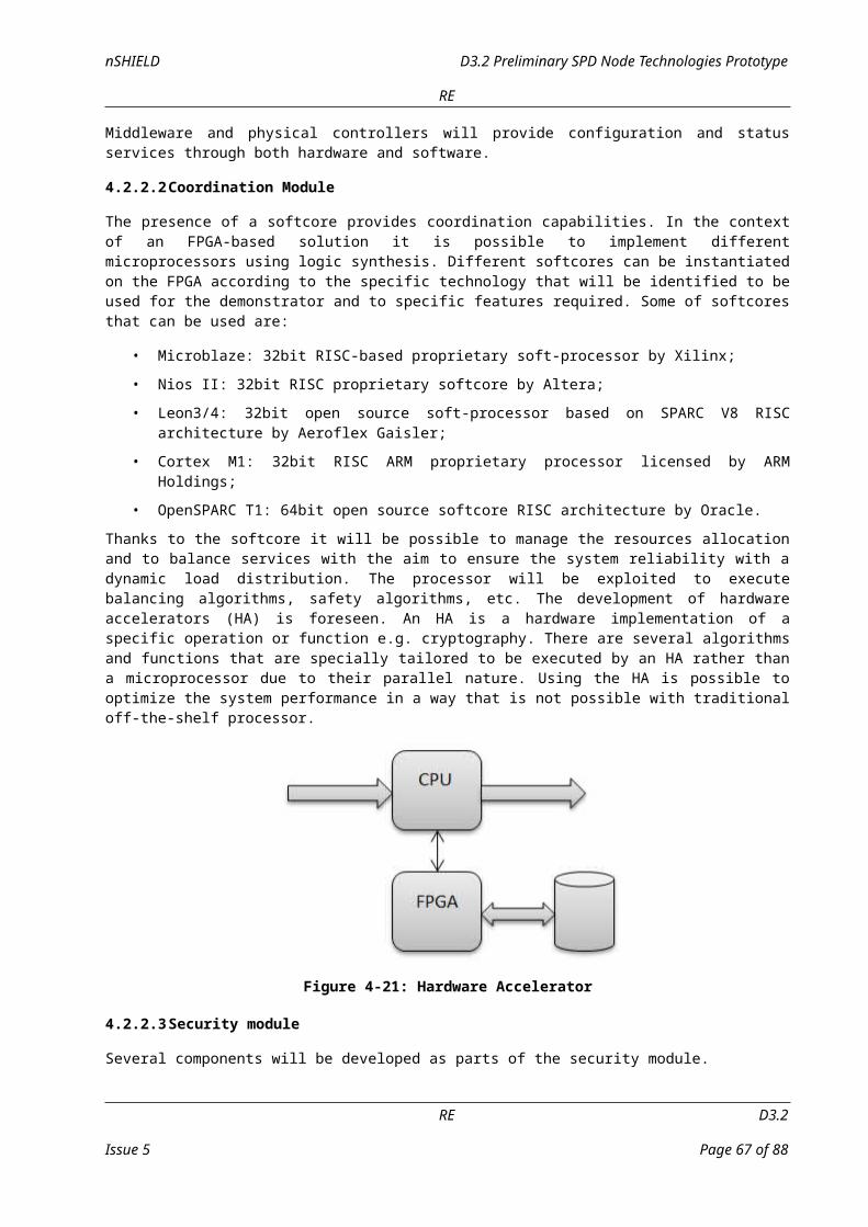
nSHIELD D3.2 Preliminary SPD Node Technologies Prototype
RE
Figure 6-29 – Tamper respondent surface enclosure
American Energy [0]19.24:
o Anti-tamper films for electronics
6.2.2 Supervisor chips
These chips provide the following monitoring capabilities:
Detection of short and open circuits (in dedicated nets or circuits).
Measurement of voltage levels (at critical points).
Temperature value and temperature change rate.
Battery leakage.
Therefore, most of these chips usually work in conjunction with some of the encapsulation methods described in 6.2.1, which act as the monitored net/circuit.
Supervisor chips must me continuously powered for right monitoring; usually requiring a current of a few µA. This involves the utilization of a dedicated battery that limits the lifetime of the device. This battery must be carefully selected regarding aspects such as capacity, self-discharge, temperature range and dimensions.
Examples of this kind of supervisor chips are:
Maxim [0]19.21:o DS36XX family
Some of these chips also provide basic secure storage features, such auto-erase small volatile memories.
Usually supervisor chips provide a digital output that change when an attack is detected. The sensitive information should be stored in the volatile memory of the supervisor or any other volatile memory that could be erased if the output is triggered. Therefore the original design of the secured device may be adapted in order to support this kind of chips.
6.2.3 Modules interfaces
As commented in previous sections, deliverable D.2.4 presents a proposal of a Reference Architecture for nSHIELD systems.
Technologies described in this section, 6.2, could be used to implement the “anti-tamper” component of the Security Module and also depend on the anti-tamper technique some attributes of the ”secure storage” could be implemented, as it is depicted in Figure 6-30.
RE D3.2
Issue 5 Page 67 of 70

D3.2 Preliminary SPD Node Technologies Prototype nSHIELD
RE
Figure 6-30: Reference architecture - Node layer (anti-tamper component)
Each component should provide some attributes. Next table summarizes the attributes that can be reported by the security module (anti-tamper and secure storage component) with this implementation:
Table 6-10: Reference architecture – Node Layer (anti-tamper attributes)
Attributes
Security module
CryptographyData integrityIdentificationAnti-tamper Secure key storage Physical path protectionSecure storage
These attributes should be reported to the monitor module or to other component of nSHIELD system. But internal interfaces need to be defined.
6.2.4 Metrics
The main metrics reported by these components, as defined in deliverable D2.5, could be the metrics related with the physical / tamper resilience (“detect” and report the presence of tamper-resistance provisions on the node) and storage of private information (boolean value depending on node’s provisions for long-term/fault-condition secure storage of private information).
Taking into account that the current list of metrics is a preliminary one, some other metrics could be added. For example:
PCB design following recommendations Boolean value Anti-tamper passive (mechanics resin) Boolean value Security level achieved by the passive anti-tamper (0 – N) Anti-tamper active (with supervisor) Boolean value Security level achieved by the active anti-tamper FIPS 140-2
6.2.5 References
20. http://www.gore.com/en_xx/products/electronic/anti-tamper/anti-tamper-respondent.html
21. http://www.maximintegrated.com/products/embedded-security/
22. http://www.freescale.com/webapp/sps/site/prod_summary.jsp?code=TWR-WIFI-G1011MI
D3.2 RE
Page 68 of 70 Issue 5

nSHIELD D3.2 Preliminary SPD Node Technologies Prototype
RE
23. http://www.maximintegrated.com/products/supervisors/
24. http://usaenergytech.com/armor-and-anti-tamper-coatings-on-flexible-substrates/
RE D3.2
Issue 5 Page 69 of 70

D3.2 Preliminary SPD Node Technologies Prototype nSHIELD
RE
7 SPD Node independent technologiesThe main research areas targeted by the node independent technologies are the following:
XXXX XXXX
XXXXXXX TO BE COMPLETED XXXXXXXXXXXX
D3.2 RE
Page 70 of 70 Issue 5