cpre281: digital logic - ece.iastate.edualexs/classes/2017_fall_281/slides_pdf/45... · digital...
TRANSCRIPT

Instructor: Alexander Stoytchev
http://www.ece.iastate.edu/~alexs/classes/
CprE 281: Digital Logic

Review for the Final Exam
CprE 281: Digital LogicIowa State University, Ames, IACopyright © Alexander Stoytchev

Administrative Stuff• The FINAL exam is scheduled for
• Wednesday Dec 13 @ 7:30 – 9:30 AM
• It will be in this room.

• The exam will cover: Chapter 1 to Chapter 6, and Sections 7.1-7.2
• Emphasis will be on Chapter 5, 6, and 7
• The exam will be open book and open notes (you can bring up to 5 pages of handwritten/typed notes) plus your textbook.
Final Exam Format

Final Exam Format
• The exam will be out of 130 points
• You need 95 points to get an A
• It will be great if you can score more than 100 points.▪ but you can’t roll over your extra points L

Topics for the Final Exam• K-maps for 2, 3, and 4 variables• Multiplexers (circuits and function)• Synthesis of logic functions using multiplexers• Shannon’s Expansion Theorem• 1’s complement and 2’s complement representation• Addition and subtraction of binary numbers• Circuits for adding and subtracting• Serial adder• Latches (circuits, behavior, timing diagrams)• Flip-Flops (circuits, behavior, timing diagrams)• Counters (up, down, synchronous, asynchronous)• Registers and Register Files

Topics for the Final Exam• Synchronous Sequential Circuits• FSMs• Moore Machines• Mealy Machines• State diagrams, state tables, state-assigned tables• State minimization• Designing a counter • Arbiter Circuits• Reverse engineering a circuit• ASM Charts• Register Machines• Bus structure and Simple Processors• Something from Star Wars

How to Study for the Final Exam• Form a study group
• Go over the slides for this class
• Go over the homeworks again
• Go over the problems at the end of Ch 5 & 6
• Exercise
• Get some sleep

Administrative Stuff
• Please check your grades on BlackBoard
• Let me know if something is wrong or missing

Sample Problems

ASM ChartsGiven an ASM chart draw the corresponding FSM

ASM ChartsGiven an ASM chart draw the corresponding FSM
C z 1 = ⁄
Reset
B z 0 = ⁄ A z 0 = ⁄ w 0 =
w 1 =
w 1 =
w 0 =
w 0 = w 1 =
[ Figure 6.3 from the textbook ][ Figure 6.82 from the textbook ]


ASM ChartsGiven an FSM draw the corresponding ASM Chart

ASM ChartsGiven an FSM draw the corresponding ASM Chart
w
w 0 1
0
1
A
B
Reset
z
[ Figure 6.83 from the textbook ][ Figure 6.23 from the textbook ]


Circuit Implementation of FSMsImplement this state-assigned Table using JK flip-flips

Circuit Implementation of FSMsImplement this state-assigned Table using JK flip-flips

[ Figure 6.94 from the textbook ]
Excitation table with JK flip-flops
Circuit Implementation of FSMsImplement this state-assigned Table using JK flip-flips


Register Machines:What does this program do?
How many balls are left in each register at the end of the program?
Register 1 Register 2 Register 3
STEP INSTRUCTION REGISTER GO TO STEP [BRANCH TO STEP]
1. Deb 3 1 22. Deb 2 3 43. Inc 3 24. End

Register Machines:Move the contents of register 2 to register 3
Register 1 Register 2 Register 3
STEP INSTRUCTION REGISTER GO TO STEP [BRANCH TO STEP]
1. Deb 3 1 22. Deb 2 3 43. Inc 3 24. End


Register 1 Register 2 Register 3
STEP INSTRUCTION REGISTER GO TO STEP [BRANCH TO STEP]
1. Deb 3 1 22. Deb 2 2 33. Deb 1 4 64. Inc 3 55. Inc 2 36. Deb 2 7 87. Inc 1 68. End
Register Machines:What does this program do?
How many balls are left in each register at the end of the program?

Register Machines:Copy the contents of register 1 to register 3
using register 2 as a temporary storage
Register 1 Register 2 Register 3
STEP INSTRUCTION REGISTER GO TO STEP [BRANCH TO STEP]
1. Deb 3 1 22. Deb 2 2 33. Deb 1 4 64. Inc 3 55. Inc 2 36. Deb 2 7 87. Inc 1 68. End


[ Figure 6.75 from the textbook ]
What does this circuit do?
D Q
Q
D Q
Q
Clock
Resetn
y 2
y 1
Y 2
Y 1
w
z

• Find the flip-flops
• Outputs of the flip-flops = present state variables
• Inputs of the flip-flops determine the next state variables
• Determine the logical expressions for the outputs
• Given this info it is easy to do the state-assigned table
• Next do the state table
• Finally, draw the state diagram.
Approach

Goal
• Given a circuit diagram for a synchronous sequential circuit, the goal is to figure out the FSM
• Figure out the present state variables, the next state variables, the state-assigned table, the state table, and finally the state diagram.
• In other words, the goal is to reverse engineer the circuit.

[ Figure 6.75 from the textbook ]
What does this circuit do?
D Q
Q
D Q
Q
Clock
Resetn
y 2
y 1
Y 2
Y 1
w
z

• Find the flip-flops
• Outputs of the flip-flops = present state variables
• Inputs of the flip-flops determine the next state variables
• Determine the logical expressions for the outputs
• Given this info it is easy to do the state-assigned table
• Next do the state table
• Finally, draw the state diagram.
Approach

[ Figure 6.75 from the textbook ]
Where are the inputs?
D Q
Q
D Q
Q
Clock
Resetn
y 2
y 1
Y 2
Y 1
w
z

[ Figure 6.75 from the textbook ]
Where are the inputs?
There isonly one input D Q
Q
D Q
Q
Clock
Resetn
y 2
y 1
Y 2
Y 1
w
z

[ Figure 6.75 from the textbook ]
Where are the outputs?
D Q
Q
D Q
Q
Clock
Resetn
y 2
y 1
Y 2
Y 1
w
z

[ Figure 6.75 from the textbook ]
Where are the outputs?
There isonly one output
D Q
Q
D Q
Q
Clock
Resetn
y 2
y 1
Y 2
Y 1
w
z

D Q
Q
D Q
Q
Clock
Resetn
y 2
y 1
Y 2
Y 1
w
z
Where kind of machine is this?Moore or Mealy?
output
input

D Q
Q
D Q
Q
Clock
Resetn
y 2
y 1
Y 2
Y 1
w
z
Moore: because the output does not depend directly on the primary input
output
input

D Q
Q
D Q
Q
Clock
Resetn
y 2
y 1
Y 2
Y 1
w
z
Where are the memory elements?

D Q
Q
D Q
Q
Clock
Resetn
y 2
y 1
Y 2
Y 1
w
z
Where are the memory elements?

D Q
Q
D Q
Q
Clock
Resetn
y 2
y 1
Y 2
Y 1
w
z
Where are the outputs of the flip-flops?

D Q
Q
D Q
Q
Clock
Resetn
y 2
y 1
Y 2
Y 1
w
z
Where are the outputs of the flip-flops?

D Q
Q
D Q
Q
Clock
Resetn
y 2
y 1
Y 2
Y 1
w
z
These are the present-state variables

D Q
Q
D Q
Q
Clock
Resetn
y 2
y 1
Y 2
Y 1
w
z
Where are the inputs of the flip-flops?

D Q
Q
D Q
Q
Clock
Resetn
y 2
y 1
Y 2
Y 1
w
z
Where are the inputs of the flip-flops?

D Q
Q
D Q
Q
Clock
Resetn
y 2
y 1
Y 2
Y 1
w
z
These are the next-state variables

D Q
Q
D Q
Q
Clock
Resetn
y 2
y 1
Y 2
Y 1
w
z
What are their logic expressions?

D Q
Q
D Q
Q
Clock
Resetn
y 2
y 1
Y 2
Y 1
w
z
What are their logic expressions?Y1 = wy1 + wy2
Y2 = wy1 + wy2

D Q
Q
D Q
Q
Clock
Resetn
y 2
y 1
Y 2
Y 1
w
z
Where is the output, again?

D Q
Q
D Q
Q
Clock
Resetn
y 2
y 1
Y 2
Y 1
w
z
Where is the output, again?

D Q
Q
D Q
Q
Clock
Resetn
y 2
y 1
Y 2
Y 1
w
z
What is its logic expression?

D Q
Q
D Q
Q
Clock
Resetn
y 2
y 1
Y 2
Y 1
w
z
What is its logic expression?
z = y1y2

This is what we have to work with now(we don’t need the circuit anymore)
z = y1y2
Y1 = wy1 + wy2
Y2 = wy1 + wy2

Let’s derive the state-assigned table
z = y1y2
Y1 = wy1 + wy2
Y2 = wy1 + wy2
Present Next State
state w = 0 w = 1 Output
y 2 y 1 Y 2 Y 1 Y 2 Y 1 z
0 0 0 1 1 0 1 1

Let’s derive the state-assigned table
z = y1y2
Y1 = wy1 + wy2
Y2 = wy1 + wy2
Present Next State
state w = 0 w = 1 Output
y 2 y 1 Y 2 Y 1 Y 2 Y 1 z
0 0 0 1 1 0 1 1

Let’s derive the state-assigned table
z = y1y2
Y1 = wy1 + wy2
Y2 = wy1 + wy2
Present Next State
state w = 0 w = 1 Output
y 2 y 1 Y 2 Y 1 Y 2 Y 1 z
0 0 0 0 1 0 1 0 0 1 1 1

Let’s derive the state-assigned table
z = y1y2
Y1 = wy1 + wy2
Y2 = wy1 + wy2
Present Next State
state w = 0 w = 1 Output
y 2 y 1 Y 2 Y 1 Y 2 Y 1 z
0 0 0 0 1 0 1 0 0 1 1 1

Let’s derive the state-assigned table
z = y1y2
Y1 = wy1 + wy2
Y2 = wy1 + wy2
Present Next State
state w = 0 w = 1 Output
y 2 y 1 Y 2 Y 1 Y 2 Y 1 z
0 0 0 1 0 0 1 0 0 0 1 0 0 1 0 1 1 0 1 1

Let’s derive the state-assigned table
z = y1y2
Y1 = wy1 + wy2
Y2 = wy1 + wy2
Present Next State
state w = 0 w = 1 Output
y 2 y 1 Y 2 Y 1 Y 2 Y 1 z
0 0 0 1 0 0 1 0 0 0 1 0 0 1 0 1 1 0 1 1

Let’s derive the state-assigned table
z = y1y2
Y1 = wy1 + wy2
Y2 = wy1 + wy2
Present Next State
state w = 0 w = 1 Output
y 2 y 1 Y 2 Y 1 Y 2 Y 1 z
0 0 0 0 0 1 0 0 1 0 0 1 0 0 1 0 0 0 1 1 0 1 1 0 0 1 1 1

We don’t need the logic expressions anymore
z = y1y2
Y1 = wy1 + wy2
Y2 = wy1 + wy2
Present Next State
state w = 0 w = 1 Output
y 2 y 1 Y 2 Y 1 Y 2 Y 1 z
0 0 0 0 0 1 0 0 1 0 0 1 0 0 1 0 0 0 1 1 0 1 1 0 0 1 1 1

We don’t need the logic expressions anymore
Present Next State
state w = 0 w = 1 Output
y 2 y 1 Y 2 Y 1 Y 2 Y 1 z
0 0 0 0 0 1 0 0 1 0 0 1 0 0 1 0 0 0 1 1 0 1 1 0 0 1 1 1

Present Next State
state w = 0 w = 1 Output
y 2 y 1 Y 2 Y 1 Y 2 Y 1 z
0 0 0 0 0 1 0 0 1 0 0 1 0 0 1 0 0 0 1 1 0 1 1 0 0 1 1 1
Let’s derive the state table
Present Next state Outputstate w = 0 w = 1 z
State-assigned table State table

Present Next State
state w = 0 w = 1 Output
y 2 y 1 Y 2 Y 1 Y 2 Y 1 z
0 0 0 0 0 1 0 0 1 0 0 1 0 0 1 0 0 0 1 1 0 1 1 0 0 1 1 1
Let’s derive the state table
Present Next state Outputstate w = 0 w = 1 z
State-assigned table State table

Present Next State
state w = 0 w = 1 Output
y 2 y 1 Y 2 Y 1 Y 2 Y 1 z
0 0 0 0 0 1 0 0 1 0 0 1 0 0 1 0 0 0 1 1 0 1 1 0 0 1 1 1
Let’s derive the state table
Present Next state Outputstate w = 0 w = 1 z
A B C D
State-assigned table State table

Present Next State
state w = 0 w = 1 Output
y 2 y 1 Y 2 Y 1 Y 2 Y 1 z
0 0 0 0 0 1 0 0 1 0 0 1 0 0 1 0 0 0 1 1 0 1 1 0 0 1 1 1
Let’s derive the state table
Present Next state Outputstate w = 0 w = 1 z
A B C D
State-assigned table State table

Present Next State
state w = 0 w = 1 Output
y 2 y 1 Y 2 Y 1 Y 2 Y 1 z
0 0 0 0 0 1 0 0 1 0 0 1 0 0 1 0 0 0 1 1 0 1 1 0 0 1 1 1
Let’s derive the state table
Present Next state Outputstate w = 0 w = 1 z
A A B A C A D A
State-assigned table State table

Present Next State
state w = 0 w = 1 Output
y 2 y 1 Y 2 Y 1 Y 2 Y 1 z
0 0 0 0 0 1 0 0 1 0 0 1 0 0 1 0 0 0 1 1 0 1 1 0 0 1 1 1
Let’s derive the state table
Present Next state Outputstate w = 0 w = 1 z
A A B A C A D A
State-assigned table State table

Present Next State
state w = 0 w = 1 Output
y 2 y 1 Y 2 Y 1 Y 2 Y 1 z
0 0 0 0 0 1 0 0 1 0 0 1 0 0 1 0 0 0 1 1 0 1 1 0 0 1 1 1
Let’s derive the state table
Present Next state Outputstate w = 0 w = 1 z
A A B B A C C A D D A D
State-assigned table State table

Present Next State
state w = 0 w = 1 Output
y 2 y 1 Y 2 Y 1 Y 2 Y 1 z
0 0 0 0 0 1 0 0 1 0 0 1 0 0 1 0 0 0 1 1 0 1 1 0 0 1 1 1
Let’s derive the state table
Present Next state Outputstate w = 0 w = 1 z
A A B B A C C A D D A D
State-assigned table State table

Present Next State
state w = 0 w = 1 Output
y 2 y 1 Y 2 Y 1 Y 2 Y 1 z
0 0 0 0 0 1 0 0 1 0 0 1 0 0 1 0 0 0 1 1 0 1 1 0 0 1 1 1
Let’s derive the state table
Present Next state Outputstate w = 0 w = 1 z
A A B B A C C A D D A D
The output is the same in both tables
State-assigned table State table

Present Next State
state w = 0 w = 1 Output
y 2 y 1 Y 2 Y 1 Y 2 Y 1 z
0 0 0 0 0 1 0 0 1 0 0 1 0 0 1 0 0 0 1 1 0 1 1 0 0 1 1 1
The two tables for the initial circuit
Present Next state Outputstate w = 0 w = 1 z
A A B 0 B A C 0 C A D 0 D A D 1
[ Figure 6.76 from the textbook ]
State-assigned table State table

Present Next State
state w = 0 w = 1 Output
y 2 y 1 Y 2 Y 1 Y 2 Y 1 z
0 0 0 0 0 1 0 0 1 0 0 1 0 0 1 0 0 0 1 1 0 1 1 0 0 1 1 1
We don’t need the state-assigned table anymore
Present Next state Outputstate w = 0 w = 1 z
A A B 0 B A C 0 C A D 0 D A D 1
[ Figure 6.76 from the textbook ]
State-assigned table State table

We don’t need the state-assigned table anymore
Present Next state Outputstate w = 0 w = 1 z
A A B 0 B A C 0 C A D 0 D A D 1
State table

Let’s Draw the State Diagram
Present Next state Outputstate w = 0 w = 1 z
A A B 0 B A C 0 C A D 0 D A D 1

Let’s Draw the State Diagram
Present Next state Outputstate w = 0 w = 1 z
A A B 0 B A C 0 C A D 0 D A D 1
A / 0
B / 0
C / 0
D / 1
Because this is a Moore machinethe output is tied to the state

Let’s Draw the State Diagram
Present Next state Outputstate w = 0 w = 1 z
A A B 0 B A C 0 C A D 0 D A D 1
A / 0
B / 0
C / 0
D / 1
All transitions when the input w is equal to 1

Let’s Draw the State Diagram
Present Next state Outputstate w = 0 w = 1 z
A A B 0 B A C 0 C A D 0 D A D 1
A / 0
B / 0
C / 0
D / 1
w=1
w=1
w=1
w=1
All transitions when the input w is equal to 1

Let’s Draw the State Diagram
Present Next state Outputstate w = 0 w = 1 z
A A B 0 B A C 0 C A D 0 D A D 1
A / 0
B / 0
C / 0
D / 1
w=1
w=1
w=1
w=1
All transitions when the input w is equal to 0

All transitions when the input w is equal to 0
Let’s Draw the State Diagram
Present Next state Outputstate w = 0 w = 1 z
A A B 0 B A C 0 C A D 0 D A D 1
A / 0
w=0
B / 0
C / 0
D / 1 w=0
w=0
w=0
w=1
w=1
w=1
w=1

We are done!
Present Next state Outputstate w = 0 w = 1 z
A A B 0 B A C 0 C A D 0 D A D 1
A / 0
w=0
B / 0
C / 0
D / 1 w=0
w=0
w=0
w=1
w=1
w=1
w=1
State diagram
State table

Almost done. What does this FSM do?
Present Next state Outputstate w = 0 w = 1 z
A A B 0 B A C 0 C A D 0 D A D 1
A / 0
w=0
B / 0
C / 0
D / 1 w=0
w=0
w=0
w=1
w=1
w=1
w=1
State diagram
State table

Almost done. What does this FSM do?
Present Next state Outputstate w = 0 w = 1 z
A A B 0 B A C 0 C A D 0 D A D 1
State table
A / 0
w=0
B / 0
C / 0
D / 1 w=0
w=0
w=0
w=1
w=1
w=1
w=1
State diagram
It sets the output z to 1 when three consecutive 1’s occur on the input w.In other words, it is a sequence detector for the input pattern 111.

Another Example(with JK flip-flops)

[ Figure 6.77 from the textbook ]
What does this circuit do?
J Q
Q
Clock
Resetn
y2
y1
J 2
J 1wz
K
J Q
QKK2
K1

• Find the flip-flops
• Outputs of the flip-flops = present state variables
• Inputs of the flip-flops determine the next state variables
• Determine the logical expressions for the outputs
• Given this info it is easy to do the state-assigned table
• Next do the state table
• Finally, draw the state diagram.
Approach

[ Figure 6.77 from the textbook ]
Where are the inputs and outputs?
J Q
Q
Clock
Resetn
y2
y1
J 2
J 1wz
K
J Q
QKK2
K1

Where are the inputs and outputs?
J Q
Q
Clock
Resetn
y2
y1
J 2
J 1wz
K
J Q
QKK2
K1 outputinput

What kind of machine is this?
J Q
Q
Clock
Resetn
y2
y1
J 2
J 1wz
K
J Q
QKK2
K1 outputinput

Where are the flip-flops?
J Q
Q
Clock
Resetn
y2
y1
J 2
J 1wz
K
J Q
QKK2
K1

Where are the flip-flops?
J Q
Q
Clock
Resetn
y2
y1
J 2
J 1wz
K
J Q
QKK2
K1

Where are the outputs of the flip-flops?
J Q
Q
Clock
Resetn
y2
y1
J 2
J 1wz
K
J Q
QKK2
K1

Where are the outputs of the flip-flops?
J Q
Q
Clock
Resetn
y2
y1
J 2
J 1wz
K
J Q
QKK2
K1

These are the next-state variables
J Q
Q
Clock
Resetn
y2
y1
J 2
J 1wz
K
J Q
QKK2
K1

Where are the inputs of the flip-flops?
J Q
Q
Clock
Resetn
y2
y1
J 2
J 1wz
K
J Q
QKK2
K1

Where are the inputs of the flip-flops?
J Q
Q
Clock
Resetn
y2
y1
J 2
J 1wz
K
J Q
QKK2
K1

What are their logic expressions?
J Q
Q
Clock
Resetn
y2
y1
J 2
J 1wz
K
J Q
QKK2
K1

What are their logic expressions?
J Q
Q
Clock
Resetn
y2
y1
J 2
J 1wz
K
J Q
QKK2
K1
J1 = w
K2 = w
J2 = w y1
K1 = w + y2

What is the logic expression of the output?
J Q
Q
Clock
Resetn
y2
y1
J 2
J 1wz
K
J Q
QKK2
K1 output

What is the logic expression of the output?
J Q
Q
Clock
Resetn
y2
y1
J 2
J 1wz
K
J Q
QKK2
K1 output
z = y1y2

This is what we have to work with now(we don’t need the circuit anymore)
z = y1y2
J1 = w
K2 = w
J2 = w y1
K1 = w + y2

Let’s derive the excitation table
z = y1y2
J1 = w
K2 = w
J2 = w y1
K1 = w + y2Present Flip-flop inputs
state w = 0 w = 1 Outputy 2 y1 J 2 K 2 J 1 K 1 J 2 K 2 J 1 K 1
z
00011011

Let’s derive the excitation table
z = y1y2
J1 = w
K2 = w
J2 = w y1
K1 = w + y2Present Flip-flop inputs
state w = 0 w = 1 Outputy 2 y1 J 2 K 2 J 1 K 1 J 2 K 2 J 1 K 1
z
00011011

Let’s derive the excitation table
z = y1y2
J1 = w
K2 = w
J2 = w y1
K1 = w + y2Present Flip-flop inputs
state w = 0 w = 1 Outputy 2 y1 J 2 K 2 J 1 K 1 J 2 K 2 J 1 K 1
z
00 0 01 0 10 0 11 1

Let’s derive the excitation table
z = y1y2
J1 = w
K2 = w
J2 = w y1
K1 = w + y2Present Flip-flop inputs
state w = 0 w = 1 Outputy 2 y1 J 2 K 2 J 1 K 1 J 2 K 2 J 1 K 1
z
00 0 01 0 10 0 11 1

Let’s derive the excitation table
z = y1y2
J1 = w
K2 = w
J2 = w y1
K1 = w + y2Present Flip-flop inputs
state w = 0 w = 1 Outputy 2 y1 J 2 K 2 J 1 K 1 J 2 K 2 J 1 K 1
z
00 0 1 1 1 0 01 0 1 1 1 0 10 0 1 1 0 0 11 0 1 1 0 1

Let’s derive the excitation table
z = y1y2
J1 = w
K2 = w
J2 = w y1
K1 = w + y2Present Flip-flop inputs
state w = 0 w = 1 Outputy 2 y1 J 2 K 2 J 1 K 1 J 2 K 2 J 1 K 1
z
00 0 1 1 1 0 01 0 1 1 1 0 10 0 1 1 0 0 11 0 1 1 0 1

The excitation table
z = y1y2
J1 = w
K2 = w
J2 = w y1
K1 = w + y2Present Flip-flop inputs
state w = 0 w = 1 Outputy 2 y1 J 2 K 2 J 1 K 1 J 2 K 2 J 1 K 1
z
00 01 0 1 0 0 1 1 0 01 01 0 1 1 0 1 1 0 10 01 0 1 0 0 1 0 0 11 01 0 1 1 0 1 0 1
[ Figure 6.78 from the textbook ]

We don’t need the logic expressions anymore
z = y1y2
J1 = w
K2 = w
J2 = w y1
K1 = w + y2Present Flip-flop inputs
state w = 0 w = 1 Outputy 2 y1 J 2 K 2 J 1 K 1 J 2 K 2 J 1 K 1
z
00 01 0 1 0 0 1 1 0 01 01 0 1 1 0 1 1 0 10 01 0 1 0 0 1 0 0 11 01 0 1 1 0 1 0 1
[ Figure 6.78 from the textbook ]

We don’t need the logic expressions anymore
Present Flip-flop inputs
state w = 0 w = 1 Outputy 2 y1 J 2 K 2 J 1 K 1 J 2 K 2 J 1 K 1
z
00 01 0 1 0 0 1 1 0 01 01 0 1 1 0 1 1 0 10 01 0 1 0 0 1 0 0 11 01 0 1 1 0 1 0 1
[ Figure 6.78 from the textbook ]

Let’s derive the state table
State table Excitation table
Present Next state Outputstate w = 0 w = 1 z

Let’s derive the state table
State table Excitation table
Present Next state Outputstate w = 0 w = 1 z
A B C D
This step is easy(map 2-bit numbers to 4 letters)

Let’s derive the state table
State table Excitation table
Present Next state Outputstate w = 0 w = 1 z
A 0 B 0 C 0 D 1
This step is easy too(the outputs are the same in both tables)

Let’s derive the state table
State table Excitation table
Present Next state Outputstate w = 0 w = 1 z
A 0 B 0 C 0 D 1
How should we do this?
?

[ Figure 5.16a from the textbook ]
JK Flip-Flop Refresher
D = JQ + KQ

[ Figure 5.16 from the textbook ]
JK Flip-Flop Refresher
J Q
Q
K01
Q t 1+( )
Q t( )0
(b) Truth table (c) Graphical symbol
J00
0 111 Q t( )1
K
D Q
Q
Q
Q
J
Clock
(a) Circuit
K

Let’s derive the state table
State table Excitation table
Present Next state Outputstate w = 0 w = 1 z
A 0 B 0 C 0 D 1
How should we do this?
?

Let’s derive the state table
Present Next state Outputstate w = 0 w = 1 z
A 0 B 0 C 0 D 1

Let’s derive the state table
Present Next state Outputstate w = 0 w = 1 z
A 0 B 0 C 0 D 1

Let’s derive the state table
Present Next state Outputstate w = 0 w = 1 z
A 0 B 0 C 0 D 1
A
Note that A = 00

Let’s derive the state table
Present Next state Outputstate w = 0 w = 1 z
A 0 B 0 C 0 D 1
A ?

Let’s derive the state table
Present Next state Outputstate w = 0 w = 1 z
A 0 B 0 C 0 D 1
A

Let’s derive the state table
Present Next state Outputstate w = 0 w = 1 z
A 0 B 0 C 0 D 1
A

Let’s derive the state table
Present Next state Outputstate w = 0 w = 1 z
A 0 B 0 C 0 D 1
A

Let’s derive the state table
Present Next state Outputstate w = 0 w = 1 z
A 0 B 0 C 0 D 1
A
= 1 = 0

Let’s derive the state table
Present Next state Outputstate w = 0 w = 1 z
A 0 B 0 C 0 D 1
A C
=0
Note that C = 10

The two tables for the initial circuit
State table
Present Next state Outputstate w = 0 w = 1 z
A A B 0 B A C 0 C A D 0 D A D 1
Excitation table

The state diagram
State table
Present Next state Outputstate w = 0 w = 1 z
A A B 0 B A C 0 C A D 0 D A D 1
A / 0
w=0
B / 0
C / 0
D / 1 w=0
w=0
w=0
w=1
w=1
w=1
w=1
State diagram

The state diagram
State table
Present Next state Outputstate w = 0 w = 1 z
A A B 0 B A C 0 C A D 0 D A D 1
A / 0
w=0
B / 0
C / 0
D / 1 w=0
w=0
w=0
w=1
w=1
w=1
w=1
State diagram
Thus, this FSM is identical to the one in the previous example, even though the circuit uses JK flip-flops.

Yet Another Example(with mixed flip-flops)

[ Figure 6.79 from the textbook ]
What does this circuit do?
Clock
Resetn
y 2
y 1 w
z
T 2
D 1
D Q
Q
T Q
Q

• Find the flip-flops
• Outputs of the flip-flops = present state variables
• Inputs of the flip-flops determine the next state variables
• Determine the logical expressions for the outputs
• Given this info it is easy to do the state-assigned table
• Next do the state table
• Finally, draw the state diagram.
Approach

[ Figure 6.79 from the textbook ]
What are the logic expressions?
Clock
Resetn
y 2
y 1 w
z
T 2
D 1
D Q
Q
T Q
Q

What are the logic expressions?
Clock
Resetn
y 2
y 1 w
z
T 2
D 1
D Q
Q
T Q
Q

What are the logic expressions?
Clock
Resetn
y 2
y 1 w
z
T 2
D 1
D Q
Q
T Q
Q
D1 = w (y1 + y2)
T2 = w y2 + w y1y2
z = y1y2

The Excitation Table
Excitation table
Present Flip-flop inputs
state w = 0 w = 1 Output
y 2 y 1 T 2 D 1 T 2 D 1 z
0 0 0 0 01 00 1 0 0 10 01 0 1 0 01 01 1 1 0 01 1
D1 = w (y1 + y2)
T2 = w y2 + w y1y2
z = y1y2

Present Next state Outputstate w = 0 w = 1 z
Present Flip-flop inputs
state w = 0 w = 1 Output
y 2 y 1 T 2 D 1 T 2 D 1 z
0 0 0 0 01 0 0 1 0 0 10 0 1 0 1 0 01 0 1 1 1 0 01 1
Let’s derive the state table

Present Next state Outputstate w = 0 w = 1 z
Present Flip-flop inputs
state w = 0 w = 1 Output
y 2 y 1 T 2 D 1 T 2 D 1 z
0 0 0 0 01 0 0 1 0 0 10 0 1 0 1 0 01 0 1 1 1 0 01 1
Let’s derive the state table
A B C D
This step is easy(map 2-bit numbers to 4 letters)

Present Next state Outputstate w = 0 w = 1 z
Present Flip-flop inputs
state w = 0 w = 1 Output
y 2 y 1 T 2 D 1 T 2 D 1 z
0 0 0 0 01 0 0 1 0 0 10 0 1 0 1 0 01 0 1 1 1 0 01 1
Let’s derive the state table
A B C D
This step is easy too(the outputs are the same in both tables)
0 0 0 1

Present Next state Outputstate w = 0 w = 1 z
Present Flip-flop inputs
state w = 0 w = 1 Output
y 2 y 1 T 2 D 1 T 2 D 1 z
0 0 0 0 01 0 0 1 0 0 10 0 1 0 1 0 01 0 1 1 1 0 01 1
Let’s derive the state table
A B C D
What should we do here?
0 0 0 1
?

Present Next state Outputstate w = 0 w = 1 z
Present Flip-flop inputs
state w = 0 w = 1 Output
y 2 y 1 T 2 D 1 T 2 D 1 z
0 0 0 0 01 0 0 1 0 0 10 0 1 0 1 0 01 0 1 1 1 0 01 1
Let’s derive the state table
A B C D
What should we do here?
0 0 0 1
?

Present Next state Outputstate w = 0 w = 1 z
Present Flip-flop inputs
state w = 0 w = 1 Output
y 2 y 1 T 2 D 1 T 2 D 1 z
0 0 0 0 01 0 0 1 0 0 10 0 1 0 1 0 01 0 1 1 1 0 01 1
Let’s derive the state table
A B C D
0 0 0 1

Present Next state Outputstate w = 0 w = 1 z
Present Flip-flop inputs
state w = 0 w = 1 Output
y 2 y 1 T 2 D 1 T 2 D 1 z
0 0 0 0 01 0 0 1 0 0 10 0 1 0 1 0 01 0 1 1 1 0 01 1
Let’s derive the state table
A B C D
0 0 0 1

Present Next state Outputstate w = 0 w = 1 z
Present Flip-flop inputs
state w = 0 w = 1 Output
y 2 y 1 T 2 D 1 T 2 D 1 z
0 0 0 0 01 0 0 1 0 0 10 0 1 0 1 0 01 0 1 1 1 0 01 1
Let’s derive the state table
A B C D
0 0 0 1

Present Next state Outputstate w = 0 w = 1 z
Present Flip-flop inputs
state w = 0 w = 1 Output
y 2 y 1 T 2 D 1 T 2 D 1 z
0 0 0 0 01 0 0 1 0 0 10 0 1 0 1 0 01 0 1 1 1 0 01 1
Let’s derive the state table
A B C D
0 0 0 1
0

Present Next state Outputstate w = 0 w = 1 z
Present Flip-flop inputs
state w = 0 w = 1 Output
y 2 y 1 T 2 D 1 T 2 D 1 z
0 0 0 0 01 0 0 1 0 0 10 0 1 0 1 0 01 0 1 1 1 0 01 1
Let’s derive the state table
A B C D
0 0 0 1
0

Present Next state Outputstate w = 0 w = 1 z
Present Flip-flop inputs
state w = 0 w = 1 Output
y 2 y 1 T 2 D 1 T 2 D 1 z
0 0 0 0 01 0 0 1 0 0 10 0 1 0 1 0 01 0 1 1 1 0 01 1
Let’s derive the state table
A B C D
0 0 0 1
0

Present Next state Outputstate w = 0 w = 1 z
Present Flip-flop inputs
state w = 0 w = 1 Output
y 2 y 1 T 2 D 1 T 2 D 1 z
0 0 0 0 01 0 0 1 0 0 10 0 1 0 1 0 01 0 1 1 1 0 01 1
Let’s derive the state table
A B C D
0 0 0 1
0
A
Note that A = 00

Present Next state Outputstate w = 0 w = 1 z
Present Flip-flop inputs
state w = 0 w = 1 Output
y 2 y 1 T 2 D 1 T 2 D 1 z
0 0 0 0 01 0 0 1 0 0 10 0 1 0 1 0 01 0 1 1 1 0 01 1
Let’s derive the state table
A B C D
What should we do here?
0 0 0 1
?
A

Present Next state Outputstate w = 0 w = 1 z
Present Flip-flop inputs
state w = 0 w = 1 Output
y 2 y 1 T 2 D 1 T 2 D 1 z
0 0 0 0 01 0 0 1 0 0 10 0 1 0 1 0 01 0 1 1 1 0 01 1
Let’s derive the state table
A B C D
0 0 0 1
A

Present Next state Outputstate w = 0 w = 1 z
Present Flip-flop inputs
state w = 0 w = 1 Output
y 2 y 1 T 2 D 1 T 2 D 1 z
0 0 0 0 01 0 0 1 0 0 10 0 1 0 1 0 01 0 1 1 1 0 01 1
Let’s derive the state table
A B C D
0 0 0 1
A

Present Next state Outputstate w = 0 w = 1 z
Present Flip-flop inputs
state w = 0 w = 1 Output
y 2 y 1 T 2 D 1 T 2 D 1 z
0 0 0 0 01 0 0 1 0 0 10 0 1 0 1 0 01 0 1 1 1 0 01 1
Let’s derive the state table
A B C D
0 0 0 1
A

Present Next state Outputstate w = 0 w = 1 z
Present Flip-flop inputs
state w = 0 w = 1 Output
y 2 y 1 T 2 D 1 T 2 D 1 z
0 0 0 0 01 0 0 1 0 0 10 0 1 0 1 0 01 0 1 1 1 0 01 1
Let’s derive the state table
A B C D
0 0 0 1
1
A

Present Next state Outputstate w = 0 w = 1 z
Present Flip-flop inputs
state w = 0 w = 1 Output
y 2 y 1 T 2 D 1 T 2 D 1 z
0 0 0 0 01 0 0 1 0 0 10 0 1 0 1 0 01 0 1 1 1 0 01 1
Let’s derive the state table
A B C D
0 0 0 1
1
A

Present Next state Outputstate w = 0 w = 1 z
Present Flip-flop inputs
state w = 0 w = 1 Output
y 2 y 1 T 2 D 1 T 2 D 1 z
0 0 0 0 01 0 0 1 0 0 10 0 1 0 1 0 01 0 1 1 1 0 01 1
Let’s derive the state table
A B C D
0 0 0 1
1
A

Present Next state Outputstate w = 0 w = 1 z
Present Flip-flop inputs
state w = 0 w = 1 Output
y 2 y 1 T 2 D 1 T 2 D 1 z
0 0 0 0 01 0 0 1 0 0 10 0 1 0 1 0 01 0 1 1 1 0 01 1
Let’s derive the state table
A B C D
0 0 0 1
1
D
Note that D = 11
A

Present Next state Outputstate w = 0 w = 1 z
A A B 0 B A C 0 C A D 0 D A D 1
Present Flip-flop inputs
state w = 0 w = 1 Output
y 2 y 1 T 2 D 1 T 2 D 1 z
0 0 0 0 01 0 0 1 0 0 10 0 1 0 1 0 01 0 1 1 1 0 01 1
Let’s derive the state table

Present Next state Outputstate w = 0 w = 1 z
A A B 0 B A C 0 C A D 0 D A D 1
Present Flip-flop inputs
state w = 0 w = 1 Output
y 2 y 1 T 2 D 1 T 2 D 1 z
0 0 0 0 01 0 0 1 0 0 10 0 1 0 1 0 01 0 1 1 1 0 01 1
The two tables for the initial circuit
State table Excitation table
[ Figure 6.80 from the textbook ][ Figure 6.75b from the textbook ]

The state diagram
State table
Present Next state Outputstate w = 0 w = 1 z
A A B 0 B A C 0 C A D 0 D A D 1
A / 0
w=0
B / 0
C / 0
D / 1 w=0
w=0
w=0
w=1
w=1
w=1
w=1
State diagram

The state diagram
State table
Present Next state Outputstate w = 0 w = 1 z
A A B 0 B A C 0 C A D 0 D A D 1
A / 0
w=0
B / 0
C / 0
D / 1 w=0
w=0
w=0
w=1
w=1
w=1
w=1
State diagram
Thus, this FSM is identical to the ones in the previous examples, even though the circuit uses JK flip-flops.


State Minimization

Present Next state Outputstate w = 0 w = 1 z
A B C 1 B D F 1 C F E 0 D B G 1 E F C 0 F E D 0 G F G 0
State Table for This Example
[ Figure 6.51 from the textbook ]

A
B C
D
E
F
G
State Diagram(just the states)

A
B C
D
E
F
G
State Diagram(transitions when w=0)

A
B C
D
E
F
G
State Diagram(transitions when w=1)

A
B C
D
E
F
Gz=1
z=1
z=1
z=0
z=0
z=0
z=0
Outputs

A
B C
D
E
F
Gz=1
z=1
z=1
z=0
z=0
z=0
z=0
Partition #1(All states in the same partition)

A
B C
D
E
F
Gz=1
z=1
z=1
z=0
z=0
z=0
z=0
Partition #1(ABCDEFG)

A
B C
D
E
F
Gz=1
z=1
z=1
z=0
z=0
z=0
z=0
Partition #2(based on outputs)
z=1 z=0

A
B C
D
E
F
Gz=1
z=1
z=1
z=0
z=0
z=0
z=0
Partition #2(ABD)(CEFG)
z=1 z=0

A
B C
D
E
F
Gz=1
z=1
z=1
z=0
z=0
z=0
z=0
Partition #3.1(Examine the 0-successors of ABD)
A
B C
D
E
F
Gz=1
z=1
z=1
z=0
z=0
z=0
z=0
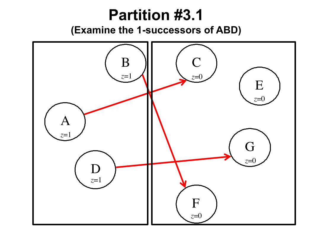
Partition #3.1(Examine the 1-successors of ABD)

A
B C
D
E
F
Gz=1
z=1
z=1
z=0
z=0
z=0
z=0
Partition #3.2(Examine the 0-successors of CEFG)

A
B C
D
E
F
Gz=1
z=1
z=1
z=0
z=0
z=0
z=0
Partition #3.2(Examine the 1-successors of CEFG)

A
B C
D
E
F
Gz=1
z=1
z=1
z=0
z=0
z=0
z=0
Partition #3.2(Examine the 1-successors of CEFG)
This needs to bein a new block

A
B C
D
E
F
Gz=1
z=1
z=1
z=0
z=0
z=0
z=0
Partition #3(ABD)(CEG)(F)

A
B C
D
E
F
Gz=1
z=1
z=1
z=0
z=0
z=0
z=0
Partition #3(ABD)(CEG)(F)

A
B C
D
E
F
Gz=1
z=1
z=1
z=0
z=0
z=0
z=0
Partition #4.1(Examine the 0-successors of ABD)

A
B C
D
E
F
Gz=1
z=1
z=1
z=0
z=0
z=0
z=0
Partition #4.1(Examine the 1-successors of ABD)

A
B C
D
E
F
Gz=1
z=1
z=1
z=0
z=0
z=0
z=0
Partition #4.1(Examine the 1-successors of ABD)
This needs to bein a new block

A
B C
D
E
F
Gz=1
z=1
z=1
z=0
z=0
z=0
z=0
Partition #4(AD)(B)(CEG)(F)

A
B C
D
E
F
Gz=1
z=1
z=1
z=0
z=0
z=0
z=0
Partition #4(AD)(B)(CEG)(F)

A
B C
D
E
F
Gz=1
z=1
z=1
z=0
z=0
z=0
z=0
Partition #5.1(Examine the 0-successors of AD)

A
B C
D
E
F
Gz=1
z=1
z=1
z=0
z=0
z=0
z=0
Partition #5.1(Examine the 1-successors of AD)

A
B C
D
E
F
Gz=1
z=1
z=1
z=0
z=0
z=0
z=0
Partition #5.2(Examine the 0-successors of B)

A
B C
D
E
F
Gz=1
z=1
z=1
z=0
z=0
z=0
z=0
Partition #5.2(Examine the 1-successors of B)

A
B C
D
E
F
Gz=1
z=1
z=1
z=0
z=0
z=0
z=0
Partition #5.3(Examine the 0-successors of CEG)

A
B C
D
E
F
Gz=1
z=1
z=1
z=0
z=0
z=0
z=0
Partition #5.3(Examine the 1-successors of CEG)

A
B C
D
E
F
Gz=1
z=1
z=1
z=0
z=0
z=0
z=0
Partition #5.4(Examine the 0-successors of F)

A
B C
D
E
F
Gz=1
z=1
z=1
z=0
z=0
z=0
z=0
Partition #5.4(Examine the 1-successors of F)

Partition #5(AD)(B)(CEG)(F)
A
B C
D
E
F
Gz=1
z=1
z=1
z=0
z=0
z=0
z=0

Partition #4(AD)(B)(CEG)(F)
A
B C
D
E
F
Gz=1
z=1
z=1
z=0
z=0
z=0
z=0

Partition #5(This is the same as #4 so we can stop here)
A
B C
D
E
F
Gz=1
z=1
z=1
z=0
z=0
z=0
z=0

Present Nextstate Outputstate w = 0 w = 1 z
A B C 1 B A F 1 C F C 0 F C A 0
[ Figure 6.52 from the textbook ]
Minimized state table

Multiplexers

4-1 Multiplexer (Definition)
• Has four inputs: w0 , w1, w2, w3
• Also has two select lines: s1 and s0
• If s1=0 and s0=0, then the output f is equal to w0
• If s1=0 and s0=1, then the output f is equal to w1
• If s1=1 and s0=0, then the output f is equal to w2
• If s1=1 and s0=1, then the output f is equal to w3

Graphical Symbol and Truth Table
[ Figure 4.2a-b from the textbook ]

0
w 0 w 1
0
1
w 2 w 3
0
1
f 0
1
s 1
s
Using three 2-to-1 multiplexers to build one 4-to-1 multiplexer
[ Figure 4.3 from the textbook ]

Implementation of a logic function
[ Figure 4.7 from the textbook ]
w3
w3
f
w1
0
w2
1
(a) Modified truth table
(b) Circuit
00011
101
fw1
0
w2
1
0 00 11 01 1
0001
0 00 11 01 1
0111
w1 w2 w3 f
00001111
w3

0 0 0 1 1 0 1 1
0 1 1 0
0 0 0 1 1 0 1 1
1 0 0 1
w 1 w 2 w 3 f
0 0 0 0 1 1 1 1
w 3
w 3
w 3
w 3
Implementation of 3-input XORwith a 4-to-1 Multiplexer
[ Figure 4.9a from the textbook ]

f
w 1
w 2
(a) Truth table (b) Circuit
0 0 0 1 1 0 1 1
0 1 1 0
0 0 0 1 1 0 1 1
1 0 0 1
w 1 w 2 w 3 f
0 0 0 0 1 1 1 1
w 3
w 3
w 3
w 3
w 3
Implementation of 3-input XORwith a 4-to-1 Multiplexer
[ Figure 4.9 from the textbook ]

Gated D Latch

[ Figure 5.7a from the textbook ]
Circuit Diagram for the Gated D Latch

Edge-Triggered D Flip-Flops

(a) Circuit
D Q
Q
Master Slave
D
Clock
Q
Q
D Q
Q
Q m Q s
Clk Clk
[ Figure 5.9a from the textbook ]
Master-Slave D Flip-Flop

D Q
Q
Master Slave
D
Clock
Q
Q
D Q
Q
Q m Q s
Clk Clk
Negative-Edge-Triggered Master-Slave D Flip-Flop
Positive-Edge-Triggered Master-Slave D Flip-Flop
D Q
Q
Master Slave
D
Clock
Q
Q
D Q
Q
Q m Q s
Clk Clk

[ Figure 5.7a from the textbook ]
Circuit Diagram for the Gated D Latch

Constructing a D Flip-Flop

Constructing a D Flip-Flop

Constructing a D Flip-Flop (with one less NOT gate)

Constructing a D Flip-Flop (with one less NOT gate)

T Flip-Flop

[ Figure 5.15a from the textbook ]
T Flip-Flop

[ Figure 5.15a from the textbook ]
T Flip-Flop
Positive-edge-triggered D Flip-Flop

[ Figure 5.15a from the textbook ]
T Flip-Flop
What is this?

What is this?
Q
Q
TD

Q
Q
T
D
What is this?
+ = ?

T
0
1 D Q
Q Clock
T Flip-Flop

What is this?
+ = ?

T D Q
Q Clock
T Flip-Flop

JK Flip-Flop

[ Figure 5.16a from the textbook ]
JK Flip-Flop
D = JQ + KQ
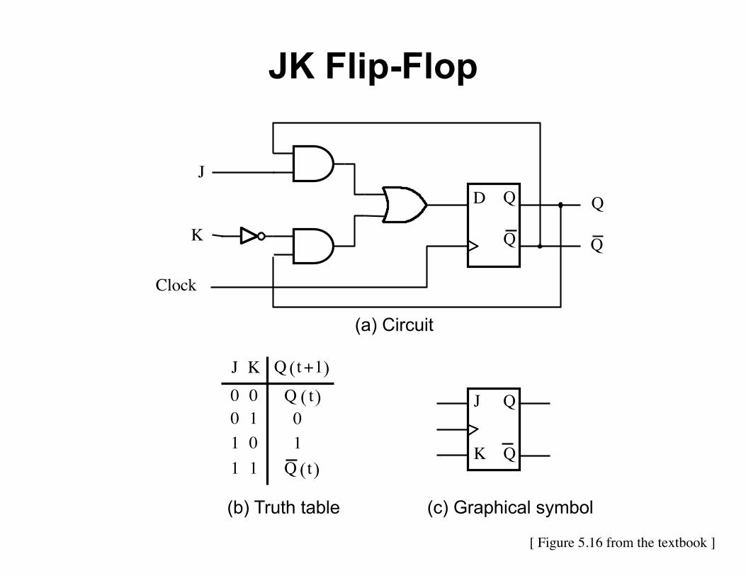
[ Figure 5.16 from the textbook ]
JK Flip-Flop
J Q
Q
K01
Q t 1+( )Q t( )
0
(b) Truth table (c) Graphical symbol
J00
0 111 Q t( )1
K
D Q
Q
Q
Q
J
Clock
(a) Circuit
K

JK Flip-Flop(How it Works)
A versatile circuit that can be used both as aSR flip-flop and as a T flip flop
If J=0 and S =0 it stays in the same state
Just like SR It can be set and reset J=S and K=R
If J=K=1 then it behaves as a T flip-flop

Registers

Register (Definition)
An n-bit structure consisting of flip-flops

A simple shift register
[ Figure 5.17 from the textbook ]
D Q
Q Clock
D Q
Q
D Q
Q
D Q
Q
In Out
t 0
t 1
t 2
t 3
t 4
t 5
t 6
t 7
1
0
1
1
1
0
0
0
0
1
0
1
1
1
0
0
0
0
1
0
1
1
1
0
0
0
0
1
0
1
1
1
0
0
0
0
1
0
1
1
Q 1 Q 2 Q 3 Q 4 Out = In
(b) A sample sequence
(a) Circuit
Q 1 Q 2 Q 3 Q 4

Parallel-access shift register
[ Figure 5.18 from the textbook ]

Counters

A three-bit up-counter
[ Figure 5.19 from the textbook ]

A three-bit up-counter
[ Figure 5.19 from the textbook ]
T Q
Q Clock
T Q
Q
T Q
Q
1
Q 0 Q 1 Q 2
(a) Circuit
Clock
Q 0
Q 1
Q 2
Count 0 1 2 3 4 5 6 7 0
(b) Timing diagram

A three-bit down-counter
[ Figure 5.20 from the textbook ]

A three-bit down-counter
[ Figure 5.20 from the textbook ]
T Q
Q Clock
T Q
Q
T Q
Q
1
Q 0 Q 1 Q 2
(a) Circuit
Clock
Q 0
Q 1
Q 2
Count 0 7 6 5 4 3 2 1 0
(b) Timing diagram

Synchronous Counters

A four-bit synchronous up-counter
[ Figure 5.21 from the textbook ]

Synchronous Counter with D Flip-Flops

A four-bit counter with D flip-flops
[ Figure 5.23 from the textbook ]

Counters with Parallel Load

A counter with parallel-load capability
[ Figure 5.24 from the textbook ]

A shift register with parallel load and enable control inputs
[ Figure 5.59 from the textbook ]

What does this circuit do?
[ Figure 5.25a from the textbook ]

Designing The Control Circuit

A Simple Processor
[ Figure 7.9 from the textbook ]

The function register and decoders
[ Figure 7.11 from the textbook ]
Clock
X0
w 0 En
y 0
w 1
y 1 y 2 y 3
1
X 1 X 2 X 3
2-to-4 decoder
Function Register
Y 0
w 0 En
y 0
w 1
y 1 y 2 y 3
1
Y 1 Y 2 Y 3
2-to-4 decoder
I 0
En
y 0 y 1 y 2 y 3
1
I 1 I 2 I 3
2-to-4 decoder
FR in
f 1 f 0 Rx1 Rx0 Ry1 Ry0
w 0 w 1
Function

A part of the control circuit for the processor
Reset Up-counter
Clear
w 0 En
y 0
w 1
y 1 y 2 y 3
1
T 1 T 2 T 3
2-to-4 decoder
Q 1 Q 0 Clock
T0
[ Figure 7.10 from the textbook ]

Control signals asserted in each time step
[ Table 7.2 from the textbook ]
T1 T2 T3
(Load): I0 ExternRin = XDone
(Move): I1 Rin = XRout = YDone
(Add): I2 Rout = XAin
Rout = YGinAddSub = 0
GoutRin = XDone
(Sub): I3 Rout = XAin
Rout = YGinAddSub = 1
GoutRin = XDone

Operations performed by this processor
[ Table 7.1 from the textbook ]
Operation Function PerformedLoad Rx, Data Rx ç Data
Move Rx, Ry Rx ç [Ry]
Add Rx, Ry Rx ç [Rx] + [Ry]
Sub Rx, Ry Rx ç [Rx] - [Ry]

Operations performed by this processor
[ Table 7.1 from the textbook ]
Operation Function PerformedLoad Rx, Data Rx ç Data
Move Rx, Ry Rx ç [Ry]
Add Rx, Ry Rx ç [Rx] + [Ry]
Sub Rx, Ry Rx ç [Rx] - [Ry]
Where Rx and Ry can be one of four possible options: R0, R1, R2, and R3

f1 f0 Function
0 0 Load
0 1 Move
1 0 Add
1 1 Sub
Rx1 Rx0 Register
0 0 R0
0 1 R1
1 0 R2
1 1 R3
Ry1 Ry0 Register
0 0 R0
0 1 R1
1 0 R2
1 1 R3
Operations performed by this processor

f1 f0 Function
0 0 Load
0 1 Move
1 0 Add
1 1 Sub
Rx1 Rx0 Register
0 0 R0
0 1 R1
1 0 R2
1 1 R3
Ry1 Ry0 Register
0 0 R0
0 1 R1
1 0 R2
1 1 R3
è Move R3, R00 1 1 1 0 0
Operations performed by this processor

f1 f0 Function
0 0 Load
0 1 Move
1 0 Add
1 1 Sub
Rx1 Rx0 Register
0 0 R0
0 1 R1
1 0 R2
1 1 R3
Ry1 Ry0 Register
0 0 R0
0 1 R1
1 0 R2
1 1 R3
è Add R1, R31 0 0 1 1 1
Operations performed by this processor

f1 f0 Function
0 0 Load
0 1 Move
1 0 Add
1 1 Sub
Rx1 Rx0 Register
0 0 R0
0 1 R1
1 0 R2
1 1 R3
Ry1 Ry0 Register
0 0 R0
0 1 R1
1 0 R2
1 1 R3
è Sub R0, R21 1 0 0 1 0
Operations performed by this processor

f1 f0 Function
0 0 Load
0 1 Move
1 0 Add
1 1 Sub
Rx1 Rx0 Register
0 0 R0
0 1 R1
1 0 R2
1 1 R3
Ry1 Ry0 Register
0 0 R0
0 1 R1
1 0 R2
1 1 R3
è Load R2, Data0 0 1 0 x x
Operations performed by this processor

Similar Encoding is Used by Modern Chips
[http://en.wikipedia.org/wiki/Instruction_set]

Sample Assembly Language ProgramFor This Processor
Move R3, R0Add R1, R3Sub R0, R2Load R2, Data

Machine Language vs Assembly Language
Move R3, R0Add R1, R3Sub R0, R2Load R2, Data
R3 ç [R0]R1 ç [R1] + [R3]R0 ç [R0] – [R2]R2 ç Data
011100100111110010001000
Machine Language Assembly Language Meaning / Interpretation

Machine Language vs Assembly Language
Move R3, R0Add R1, R3Sub R0, R2Load R2, Data
R3 ç [R0]R1 ç [R1] + [R3]R0 ç [R0] – [R2]R2 ç Data
011100100111110010001000
Machine Language Assembly Language Meaning / Interpretation

Machine Language vs Assembly Language
Move R3, R0Add R1, R3Sub R0, R2Load R2, Data
R3 ç [R0]R1 ç [R1] + [R3]R0 ç [R0] – [R2]R2 ç Data
011100100111110010001000
Machine Language Assembly Language Meaning / Interpretation
For short, each line can be expresses as a hexadecimal number

Machine Language vs Assembly Language
Move R3, R0Add R1, R3Sub R0, R2Load R2, Data
R3 ç [R0]R1 ç [R1] + [R3]R0 ç [R0] – [R2]R2 ç Data
1C273208
Machine Language Assembly Language Meaning / Interpretation

Questions?

THE END